WO2021192176A1 - Image capturing device - Google Patents
Image capturing device Download PDFInfo
- Publication number
- WO2021192176A1 WO2021192176A1 PCT/JP2020/013789 JP2020013789W WO2021192176A1 WO 2021192176 A1 WO2021192176 A1 WO 2021192176A1 JP 2020013789 W JP2020013789 W JP 2020013789W WO 2021192176 A1 WO2021192176 A1 WO 2021192176A1
- Authority
- WO
- WIPO (PCT)
- Prior art keywords
- pixel
- read
- image
- signal
- circuit
- Prior art date
Links
- 238000012545 processing Methods 0.000 claims abstract description 133
- 238000000034 method Methods 0.000 claims abstract description 110
- 230000008569 process Effects 0.000 claims abstract description 36
- 238000006243 chemical reaction Methods 0.000 claims description 94
- 238000012937 correction Methods 0.000 claims description 66
- 238000003384 imaging method Methods 0.000 claims description 53
- 238000003705 background correction Methods 0.000 claims description 43
- 239000003086 colorant Substances 0.000 claims description 14
- 230000003287 optical effect Effects 0.000 claims description 13
- 239000000654 additive Substances 0.000 claims description 10
- 230000000996 additive effect Effects 0.000 claims description 10
- 239000000284 extract Substances 0.000 claims description 7
- 239000000203 mixture Substances 0.000 description 62
- 238000001514 detection method Methods 0.000 description 37
- 238000009792 diffusion process Methods 0.000 description 34
- 230000000875 corresponding effect Effects 0.000 description 32
- 230000006870 function Effects 0.000 description 15
- 230000007246 mechanism Effects 0.000 description 13
- 238000010586 diagram Methods 0.000 description 10
- 230000006835 compression Effects 0.000 description 9
- 238000007906 compression Methods 0.000 description 9
- 230000008707 rearrangement Effects 0.000 description 7
- 230000002596 correlated effect Effects 0.000 description 5
- 230000006837 decompression Effects 0.000 description 5
- 230000007547 defect Effects 0.000 description 5
- 230000007274 generation of a signal involved in cell-cell signaling Effects 0.000 description 5
- 238000003702 image correction Methods 0.000 description 5
- 210000001747 pupil Anatomy 0.000 description 5
- 238000005070 sampling Methods 0.000 description 5
- 230000015572 biosynthetic process Effects 0.000 description 4
- 230000008859 change Effects 0.000 description 4
- 230000035945 sensitivity Effects 0.000 description 4
- 238000003786 synthesis reaction Methods 0.000 description 4
- 238000012546 transfer Methods 0.000 description 4
- 238000012935 Averaging Methods 0.000 description 3
- 230000001276 controlling effect Effects 0.000 description 3
- 102100032257 E3 ubiquitin-protein ligase Mdm2 Human genes 0.000 description 2
- 108050002772 E3 ubiquitin-protein ligase Mdm2 Proteins 0.000 description 2
- 230000000295 complement effect Effects 0.000 description 2
- 230000002950 deficient Effects 0.000 description 2
- 238000005516 engineering process Methods 0.000 description 2
- 230000001133 acceleration Effects 0.000 description 1
- 230000003321 amplification Effects 0.000 description 1
- 239000002131 composite material Substances 0.000 description 1
- 230000006866 deterioration Effects 0.000 description 1
- 230000000694 effects Effects 0.000 description 1
- 230000004907 flux Effects 0.000 description 1
- 239000011159 matrix material Substances 0.000 description 1
- 238000012986 modification Methods 0.000 description 1
- 230000004048 modification Effects 0.000 description 1
- 238000003199 nucleic acid amplification method Methods 0.000 description 1
- 230000003595 spectral effect Effects 0.000 description 1
- 239000003039 volatile agent Substances 0.000 description 1
Images


Classifications
-
- H—ELECTRICITY
- H04—ELECTRIC COMMUNICATION TECHNIQUE
- H04N—PICTORIAL COMMUNICATION, e.g. TELEVISION
- H04N25/00—Circuitry of solid-state image sensors [SSIS]; Control thereof
- H04N25/60—Noise processing, e.g. detecting, correcting, reducing or removing noise
- H04N25/63—Noise processing, e.g. detecting, correcting, reducing or removing noise applied to dark current
-
- G—PHYSICS
- G02—OPTICS
- G02B—OPTICAL ELEMENTS, SYSTEMS OR APPARATUS
- G02B7/00—Mountings, adjusting means, or light-tight connections, for optical elements
- G02B7/28—Systems for automatic generation of focusing signals
- G02B7/34—Systems for automatic generation of focusing signals using different areas in a pupil plane
-
- G—PHYSICS
- G03—PHOTOGRAPHY; CINEMATOGRAPHY; ANALOGOUS TECHNIQUES USING WAVES OTHER THAN OPTICAL WAVES; ELECTROGRAPHY; HOLOGRAPHY
- G03B—APPARATUS OR ARRANGEMENTS FOR TAKING PHOTOGRAPHS OR FOR PROJECTING OR VIEWING THEM; APPARATUS OR ARRANGEMENTS EMPLOYING ANALOGOUS TECHNIQUES USING WAVES OTHER THAN OPTICAL WAVES; ACCESSORIES THEREFOR
- G03B13/00—Viewfinders; Focusing aids for cameras; Means for focusing for cameras; Autofocus systems for cameras
- G03B13/32—Means for focusing
- G03B13/34—Power focusing
- G03B13/36—Autofocus systems
-
- H—ELECTRICITY
- H01—ELECTRIC ELEMENTS
- H01L—SEMICONDUCTOR DEVICES NOT COVERED BY CLASS H10
- H01L27/00—Devices consisting of a plurality of semiconductor or other solid-state components formed in or on a common substrate
- H01L27/14—Devices consisting of a plurality of semiconductor or other solid-state components formed in or on a common substrate including semiconductor components sensitive to infrared radiation, light, electromagnetic radiation of shorter wavelength or corpuscular radiation and specially adapted either for the conversion of the energy of such radiation into electrical energy or for the control of electrical energy by such radiation
- H01L27/144—Devices controlled by radiation
- H01L27/146—Imager structures
- H01L27/14601—Structural or functional details thereof
- H01L27/1462—Coatings
- H01L27/14621—Colour filter arrangements
-
- H—ELECTRICITY
- H04—ELECTRIC COMMUNICATION TECHNIQUE
- H04N—PICTORIAL COMMUNICATION, e.g. TELEVISION
- H04N23/00—Cameras or camera modules comprising electronic image sensors; Control thereof
-
- H—ELECTRICITY
- H04—ELECTRIC COMMUNICATION TECHNIQUE
- H04N—PICTORIAL COMMUNICATION, e.g. TELEVISION
- H04N23/00—Cameras or camera modules comprising electronic image sensors; Control thereof
- H04N23/60—Control of cameras or camera modules
-
- H—ELECTRICITY
- H04—ELECTRIC COMMUNICATION TECHNIQUE
- H04N—PICTORIAL COMMUNICATION, e.g. TELEVISION
- H04N25/00—Circuitry of solid-state image sensors [SSIS]; Control thereof
- H04N25/40—Extracting pixel data from image sensors by controlling scanning circuits, e.g. by modifying the number of pixels sampled or to be sampled
- H04N25/42—Extracting pixel data from image sensors by controlling scanning circuits, e.g. by modifying the number of pixels sampled or to be sampled by switching between different modes of operation using different resolutions or aspect ratios, e.g. switching between interlaced and non-interlaced mode
-
- H—ELECTRICITY
- H04—ELECTRIC COMMUNICATION TECHNIQUE
- H04N—PICTORIAL COMMUNICATION, e.g. TELEVISION
- H04N25/00—Circuitry of solid-state image sensors [SSIS]; Control thereof
- H04N25/40—Extracting pixel data from image sensors by controlling scanning circuits, e.g. by modifying the number of pixels sampled or to be sampled
- H04N25/44—Extracting pixel data from image sensors by controlling scanning circuits, e.g. by modifying the number of pixels sampled or to be sampled by partially reading an SSIS array
- H04N25/445—Extracting pixel data from image sensors by controlling scanning circuits, e.g. by modifying the number of pixels sampled or to be sampled by partially reading an SSIS array by skipping some contiguous pixels within the read portion of the array
-
- H—ELECTRICITY
- H04—ELECTRIC COMMUNICATION TECHNIQUE
- H04N—PICTORIAL COMMUNICATION, e.g. TELEVISION
- H04N25/00—Circuitry of solid-state image sensors [SSIS]; Control thereof
- H04N25/40—Extracting pixel data from image sensors by controlling scanning circuits, e.g. by modifying the number of pixels sampled or to be sampled
- H04N25/46—Extracting pixel data from image sensors by controlling scanning circuits, e.g. by modifying the number of pixels sampled or to be sampled by combining or binning pixels
-
- H—ELECTRICITY
- H04—ELECTRIC COMMUNICATION TECHNIQUE
- H04N—PICTORIAL COMMUNICATION, e.g. TELEVISION
- H04N25/00—Circuitry of solid-state image sensors [SSIS]; Control thereof
- H04N25/60—Noise processing, e.g. detecting, correcting, reducing or removing noise
- H04N25/63—Noise processing, e.g. detecting, correcting, reducing or removing noise applied to dark current
- H04N25/633—Noise processing, e.g. detecting, correcting, reducing or removing noise applied to dark current by using optical black pixels
-
- H—ELECTRICITY
- H04—ELECTRIC COMMUNICATION TECHNIQUE
- H04N—PICTORIAL COMMUNICATION, e.g. TELEVISION
- H04N25/00—Circuitry of solid-state image sensors [SSIS]; Control thereof
- H04N25/70—SSIS architectures; Circuits associated therewith
- H04N25/703—SSIS architectures incorporating pixels for producing signals other than image signals
- H04N25/704—Pixels specially adapted for focusing, e.g. phase difference pixel sets
Definitions
- the present invention relates to an imaging device including an image sensor in which pixels are divided into a plurality of pixels.
- imaging devices such as digital cameras equipped with an image plane phase difference image sensor and performing image plane phase difference AF have become widespread.
- the image plane phase difference AF focuses from the current focus position without searching for the peak of the contrast value. Since the drive direction and the required drive amount of the focus lens for the purpose can be acquired, there is a feature that the focus can be adjusted at high speed.
- the pupil-divided light beam is photoelectrically converted by a photoelectric conversion element (an example of the photoelectric conversion element is a photodiode (PD), which is hereinafter referred to as PD for simplicity). It enables phase difference detection.
- a photoelectric conversion element an example of the photoelectric conversion element is a photodiode (PD), which is hereinafter referred to as PD for simplicity.
- PD photodiode
- the light-shielding image plane phase difference image sensor has a light-shielding structure that blocks a part of the light rays incident on the PD arranged under the microlens in the pixel, and the light rays incident from the photographing lens are captured by the pupil according to the arrangement of the light-shielding structure. It is a division method.
- the PD division type image plane phase difference image sensor is a method in which the light rays incident from the photographing lens are divided into pupils by dividing the PD in the pixel instead of having a light-shielding structure.
- the pupil division method in the PD division method is performed by changing the PD division method.
- pixel data for left pupil division is generated by adding and averaging a part of the 9-divided PD signal, and the other part is added and averaged.
- the pair for detecting the phase difference (for example, left and right pair, upper and lower pair, etc.) can be configured within one pixel, whereas in the light-shielding image plane phase difference image sensor, within one pixel. Since it cannot be configured and requires a plurality of pixels, the former can significantly improve the focus detection accuracy as compared with the latter.
- the number of PDs does not change in the light-shielding image plane phase difference image sensor as compared with the non-image plane phase difference image sensor, but the PD division type image plane phase difference image sensor corresponds to the number of pixel divisions n.
- the number of PDs increases n times.
- the PD division type image plane phase difference image sensor has n times the signal reading time as compared with the light-shielding type image plane phase difference image sensor (and the non-image plane phase difference image sensor), and the imaging rate and the imaging rate and the image sensor are increased.
- the acquisition rate of the phase difference information becomes 1 / n.
- the present invention has been made in view of the above circumstances, and provides an imaging device including an image sensor in which pixels are divided into a plurality of pixels, which can acquire phase difference information while suppressing a decrease in imaging rate. I am aiming.
- the imaging device when a plurality of pixels are arranged in a row direction and a direction in which the row direction intersects, and n is an integer of 2 or more, the plurality of pixels are each one microlens.
- An image that includes n photoelectric conversion elements and outputs an imaging signal related to n divided pixel signals generated by photoelectric conversion of light from the microlens by the n photoelectric conversion elements.
- the image sensor includes a sensor and an image processing circuit for image processing the imaging signal output from the image sensor, and the image sensor has the n for each pixel row composed of a plurality of pixels arranged in the row direction.
- the image pickup signal related to the divided pixel signals can be read out in the first read mode or the second read mode, and the first read mode is one by adding the n divided pixel signals.
- the second read mode n signals are generated from the n divided pixel signals and one pixel row is read in n rows.
- the image processing circuit processes the pixel signals of the pixel rows read in the first read mode and the n signals of the pixel rows read in the second read mode. , Generates image data in which pixel data is arranged in a predetermined order for each pixel row.
- the timing chart which shows the operation of the reading circuit of 1PD region in the image sensor of the said embodiment.
- the timing chart which shows the operation in the normal reading method of the reading circuit of the 2PD region in the image sensor of the said embodiment.
- the timing chart which shows the operation in the addition reading method of the reading circuit of the 2PD area in the image sensor of the said embodiment.
- the divided pixel signal read from the 2PD area and the pixel signal read from the 1PD area when the image sensor operates in the normal reading method and the image sensor has one OB clamp circuit.
- the pixel signal (L + R) read from the 2PD area and the pixel signal ALL read from the 1PD area of the image sensor operating in the additive reading method are OB clamped by one OB clamp circuit.
- the pixel signal (L + R) read from the 2PD area and the pixel signal ALL read from the 1PD area of the image sensor operating in the additive reading method are OB due to the difference in the CDS period.
- FIG. 1 to 15 show an embodiment of the present invention
- FIG. 1 is a block diagram showing a configuration of an image pickup apparatus.
- FIG. 1 shows an example in which the image pickup device is configured as, for example, a digital camera
- the image pickup device is not limited to the digital camera, and the digital video camera, the telephone device with a shooting function, the electronic endoscope, and the like.
- Any of various devices having an imaging function such as a microscope with an imaging function and a telescope with an imaging function, may be used.
- this image pickup apparatus includes a lens 1, an image sensor 2, an image processing circuit 3, a display 4, a camera shake sensor 6, a camera shake correction mechanism 7, a focus control mechanism 8, and the like. It includes a camera operating device 9 and a camera controller 10.
- the recording memory 5 is also shown in FIG. 1, the recording memory 5 may be configured to be detachable from the imaging device, and therefore is not unique to the imaging device. May be good.
- the lens 1 is an imaging optical system that forms an optical image of a subject on an image sensor 2.
- the lens 1 includes one or more lenses including a focus lens for adjusting the focus position (focus position) for focusing, and an aperture for controlling the range of the passing luminous flux.
- the camera shake correction function is also provided.
- a mechanical shutter for controlling the exposure time is further provided between the lens 1 and the image sensor 2.
- the image sensor 2 is arranged on the optical path of the photographing optical axis of the lens 1, and photoelectrically converts the optical image of the subject imaged by the lens 1 and outputs it as an imaging signal which is an electric signal.
- the image sensor 2 is arranged in a row direction and a direction in which a plurality of pixels intersect in the row direction.
- An example of the direction intersecting the row direction is a direction orthogonal to the row direction (column direction), but the direction is not limited to this, and the direction diagonally intersects the row direction (for example, arrangement of a so-called honeycomb structure). ) Etc. may be used.
- the plurality of pixels provided in the image sensor 2 are each a microlens ML (see FIG. 3), n photoelectric conversion elements PD (see FIG. 3), and n. It has. It should be noted that a general optical lens is usually composed of a plurality of lenses along the optical axis direction. Therefore, even in the case of a microlens ML composed of a plurality of lenses along the optical axis direction, it is counted as one microlens ML.
- the image sensor 2 outputs an imaging signal related to n divided pixel signals generated by photoelectric conversion of light from the microlens ML by n photoelectric conversion elements PD.
- the imaging signal related to the n divided pixel signals for example, when one pixel is divided into L (left) and R (right), the n divided pixel signals themselves (divided pixels).
- Signal L and divided pixel signal R signals that can configure n divided pixel signals (pixel signal (L + R) and divided pixel signal L) (or pixel signal (L + R) and divided pixel signal R) n divisions
- pixel signal (L + R) from 2PD region
- pixel signal ALL from 1PD region
- the image sensor 2 is a color image sensor in which color filters of a plurality of filter colors are arranged as repetitions of a predetermined basic arrangement so that one filter color corresponds to one microlens ML.
- the image sensor 2 is not limited to the color image sensor, and may be a monochrome image sensor.
- the predetermined basic array of the image sensor 2 is, for example, a Bayer array of 2 ⁇ 2 pixels (primary color Bayer array, complementary color Bayer array, etc.), but the present invention is not limited to this, and a basic array of 6 ⁇ 6 pixels may be used. I do not care. In the present embodiment, the case where the predetermined basic arrangement is the primary color Bayer arrangement will be described.
- the image sensor 2 is a so-called PD division type image plane phase difference image sensor in which the pixels are divided into a plurality of divided pixels.
- FIG. 3 is a chart showing an example of a 2-division and 4-division pixel division configuration and a read circuit in the image sensor 2.
- the primary color Bayer array is a basic array of 2 vertical x 2 horizontal pixels, and the basic array is periodically repeated in the row direction and the column direction.
- the green filters Gr and Gb are arranged diagonally, the red filter Rr is arranged in the same row as the green filter Gr, and the blue filter Bb is arranged in the same row as the green filter Gb. be.
- the green filter Gr and the green filter Gb have the same spectral characteristics, but they are distinguished according to which of the red filter Rr and the blue filter Bb has the same line.
- the filter color red is described as Rr
- blue is also described as Bb.
- one pixel includes a color filter of any one of the four filter colors Rr, Gr, Gb, and Bb, and one microlens ML.
- one photoelectric conversion element PD corresponds to one pixel.
- the plurality of pixels provided in the image sensor 2 are light-shielded by forming a light-shielding film or the like on the entire surface of the normal pixel and the light-receiving portion of the pixel.
- OB Optical Black: optical black
- An example of arranging the normal pixels and the OB pixels will be described later with reference to FIG.
- the first column of FIG. 3 shows an example in which one pixel is divided into two parts, right (R) and left (L).
- the side-by-side arrangement of the tables is referred to as columns 1 to 3 in order from top to bottom.
- the arrangement of n photoelectric conversion elements PD with respect to one microlens ML is referred to as a divided arrangement.
- This RL division arrangement is suitable for horizontal phase difference detection (so-called vertical line detection).
- each filter color Rr, Gr, Gb, Bb two divided photoelectric conversion element PDs, that is, a photoelectric conversion element PDL on the left side and a photoelectric conversion element PDR on the right side are provided, respectively.
- Each photoelectric conversion element PDL and PDR is configured as, for example, a photodiode, and photoelectrically converts incident light to generate an electric charge.
- Each photoelectric conversion element PDL and PDR are connected to a floating diffusion FD via transistors TrL and TrR that function as read switches, respectively.
- the charge of only one of the photoelectric conversion elements PDL and PDR is transferred to the floating diffusion FD, and the divided pixel signal L is described later.
- the divided pixel signal R can be read out.
- the charges of the photoelectric conversion elements PDL and PDR are transferred to the floating diffusion FD, that is, the charges of the two photoelectric conversion elements PDL and PDR are added to each other, which is usually ( The pixel signal of L + R) can be read out.
- the floating diffusion FD and the transistors TrL and TrR are connected to the power supply voltage VDD via the transistor TrRES that functions as a reset switch. By turning on the transistor TrRES, the floating diffusion FD is reset. At this time, if the transistors TrL and TrR are turned on at the same time, the photoelectric conversion elements PDL and PDR are also reset.
- the floating diffusion FD is connected to the vertical signal line VSL via the transistor TrAMP and the transistor TrSEL.
- the transistor TrAMP is connected to the power supply voltage VDD and is connected to a constant current circuit (not shown) via the transistor TrSEL to function as an amplifier circuit, and the transistor TrSEL functions as a selection switch.
- the transistor TrSEL by turning on the transistor TrSEL, the voltage value of the floating diffusion FD is amplified by the transistor TrAMP and read from the vertical signal line VSL.
- the second column of FIG. 3 shows an example in which one pixel is divided into upper (U) and lower (D).
- each photoelectric conversion element PDs that is, an upper photoelectric conversion element PDU and a lower photoelectric conversion element PDD are provided, respectively. ..
- Each photoelectric conversion element PDU and PDD is configured as, for example, a photodiode, and photoelectrically converts incident light to generate an electric charge.
- the read circuit is the same as in the case of RL2 division, except that the LR is UD.
- the U-divided pixel signal or the D-divided pixel signal can be read out.
- the third column of FIG. 3 shows an example in which one pixel is divided into four parts, right (R), left (L), upper (U), and lower (D).
- n 4 of the divided arrangements shown in the third column: upper left (LU), upper right (RU), lower left (LD), and lower right (RD).
- This 4-split arrangement is suitable for both horizontal phase difference detection (so-called vertical line detection) and vertical phase difference detection (so-called horizontal line detection).
- the photoelectric conversion element PD having four divided arrangements, that is, the photoelectric conversion element PDLU on the upper left side, the photoelectric conversion element PDRU on the upper right side, and the photoelectric on the lower left side.
- a conversion element PDLD and a photoelectric conversion element PDRD on the lower right side are provided, respectively.
- Each photoelectric conversion element PDLU, PDRU, PDLD, PDRD is configured as, for example, a photodiode, and photoelectrically converts incident light to generate an electric charge.
- Each photoelectric conversion element PDLU, PDRU, PDLD, PDRD is connected to a floating diffusion FD via transistors TrLU, TrRU, TrLD, and TrRD that function as read switches, respectively.
- the charge of only one of the photoelectric conversion elements PDLU, PDRU, PDLD, and PDRD is transferred to the floating diffusion FD, and the LU division pixel. It can be read as a signal, a RU-divided pixel signal, an LD-divided pixel signal, or an RD-divided pixel signal.
- the L (LU + LD) divided pixel signal and the R (RU + RD) divided pixel signal can be read out.
- a U (LU + RU) divided pixel signal and a D (LD + RD) divided pixel signal can be read out.
- a normal (LU + RU + LD + RD) pixel signal can be read out.
- the floating diffusion FD and the transistors TrLU, TrRU, TrLD, and TrRD are connected to the power supply voltage VDD via the transistor TrRES that functions as a reset switch. By turning on the transistor TrRES, the floating diffusion FD is reset. At this time, if the transistors TrLU, TrRU, TrLD, and TrRD are turned on at the same time, the photoelectric conversion elements PDLU, PDRU, PDLD, and PDRD are also reset.
- the floating diffusion FD is vertical via a transistor TrAMP which is connected to a power supply voltage VDD and is connected to a constant current circuit (not shown) via a transistor TrSEL to function as an amplifier circuit and a transistor TrSEL which functions as a selection switch. It is connected to the signal line VSL.
- the transistor TrSEL by turning on the transistor TrSEL, the voltage value of the floating diffusion FD is amplified by the transistor TrAMP and read from the vertical signal line VSL.
- a normal image sensor without pixel division is used. It can be read with the same read time as when the pixel signal is read from, but phase difference information cannot be obtained.
- the pixel signal is generated and read by adding the divided pixels, and the two divisions are performed.
- the reading time is about twice as long, and in the case of four divisions, the reading time is about four times as long, so that the imaging rate is lowered.
- the image sensor 2 of the present embodiment reads the imaging signal related to n divided pixel signals in the first read mode or the second read mode for each pixel row composed of a plurality of pixels arranged in the row direction. (A certain pixel row is read in the first read mode, and another pixel row is read in the second read mode). Such a read mode will be appropriately referred to as a high-speed video phase difference read mode.
- the image sensor 2 reads the image pickup signal of the normal pixel in the first read mode and the second read mode (a certain normal pixel line is read in the first read mode, and the other is read.
- the image pickup signal of the OB pixel is read in the first read mode and the second read mode (a certain OB pixel line is read in the first read mode, and the other is read.
- the first read mode is a mode in which n divided pixel signals are added to generate one pixel signal, and one pixel line is read by one line.
- a pixel signal equivalent to a state in which one pixel is composed of only one photoelectric conversion element PD (that is, not divided) is output. Therefore, "1PD" is appropriately used. It is described as.
- the second read mode is a mode in which n signals are generated from n divided pixel signals and one pixel line is read with n lines or less natural number (integer of 1 or more) lines.
- n lines or less natural number integer of 1 or more lines.
- there are two reading modes a normal reading method and an additive reading method. Regardless of which method is used, n or less natural numbers (integers of 1 or more) are used. ) Is output, so the number of read lines is used as appropriate.
- the image sensor 2 of the present embodiment can also operate in the video read mode and the all-phase difference read mode described above, but the case of operating in the high-speed video phase difference read mode will be described below.
- the image pickup signal read from the read circuit is converted into a digital signal by a column-parallel A / D converter (so-called column ADC) provided in the image sensor 2 (not shown), and the OB provided in the image sensor 2
- the OB level is set to a predetermined target level (OB clamp level) (fixed value) by the clamp circuit 2a.
- OB clamp level predetermined target level
- the column ADC and the OB clamp circuit 2a are not limited to be provided one by one, but may be provided in plurality in order to improve the reading speed or the like.
- the image processing circuit 3 inputs an imaging signal (an imaging signal related to n divided pixel signals generated by the n photoelectric conversion elements PD) output from the image sensor 2, and various types of input signals are input. Image processing is performed to generate an image signal for display or recording.
- the display 4 is a display device that displays an image based on a signal that has been image-processed for display by the image processing circuit 3.
- the display 4 displays a live view, a rec-view display of a still image after shooting, a playback display of a recorded still image, a display during video recording, a playback display of a recorded moving image, and the like, and is used on the imaging device.
- Various kinds of related information are also displayed.
- the recording memory 5 is for storing signals (still image signals, moving image signals, etc.) image-processed for recording by the image processing circuit 3, and is, for example, a memory card that can be attached to and detached from an image pickup device, or an image pickup. It is composed of a non-volatile memory or the like provided inside the device.
- the hand shake sensor 6 is a sensing device that includes an acceleration sensor, an angular velocity sensor, and the like, detects the hand shake of the image pickup device, and outputs the camera shake to the camera controller 10.
- the camera shake correction mechanism 7 moves at least one of the lens 1 and the image sensor 2 by an actuator or the like so as to cancel the camera shake detected by the hand shake sensor 6, and the image sensor 2 It is a mechanical mechanism that reduces the influence of camera shake on the optical subject image that is imaged on the lens.
- the focus control mechanism 8 is a mechanical mechanism that drives the focus lens included in the lens 1 based on the control of the camera controller 10 so that the subject image formed on the image sensor 2 comes into focus. Further, the focus control mechanism 8 outputs lens drive information such as a lens position to the camera controller 10.
- the camera operation device 9 is an input device for performing various operations on the image pickup device.
- the camera operating device 9 has, for example, a power switch for turning on / off the power of the image pickup device, a release button for instructing and inputting still image shooting or movie shooting, a still image shooting mode, a movie shooting mode, and a live view.
- Operation members such as mode buttons for setting the mode, still image / video playback mode, and operation buttons for setting the type of file to be recorded (JPEG image file, RAW image file, or a combination thereof, etc.) include.
- the camera controller 10 includes information from the image processing circuit 3 (including information such as exposure level, contrast, and phase difference as described later), camera shake information from the hand shake sensor 6, and lens drive from the focus control mechanism 8. Based on information, input from the camera operating device 9, etc., the entire image pickup device including the lens 1, the image sensor 2, the image processing circuit 3, the recording memory 5, the camera shake correction mechanism 7, the focus control mechanism 8, etc. is controlled. Is what you do.
- the camera controller 10 drives and controls the image sensor 2 to perform imaging. Further, the camera controller 10 controls the aperture of the lens 1 based on the exposure level information.
- the camera controller 10 controls the focus control mechanism 8 based on the contrast or phase difference information, drives the focus lens of the lens 1, and causes autofocus by contrast AF or phase difference AF.
- FIG. 2 is a block diagram showing the configuration of the image processing circuit 3.
- the image processing circuit 3 includes an image data generation circuit 11, a first image processing circuit 12, a memory 13, and a second image processing circuit 14.
- the image data generation circuit 11 generates image data by performing correction processing or the like according to the characteristics of the image sensor on the image pickup signal output from the image sensor 2.
- the first image processing circuit 12 performs processing related to resizing, AE (automatic exposure), and AF (autofocus) based on the signal output from the image data generation circuit 11.
- the memory 13 is a frame memory that stores image data processed or in the process of being processed by the image data generation circuit 11, the first image processing circuit 12, and the second image processing circuit 14, and is, for example, a RAM (Random Access Memory). It is configured to include a volatile storage portion such as, and a non-volatile storage portion such as FROM (Flash ROM: flash memory (registered trademark) (flash memory)).
- a volatile storage portion such as, and a non-volatile storage portion such as FROM (Flash ROM: flash memory (registered trademark) (flash memory)).
- Flash ROM flash memory
- various data stored in the non-volatile storage portion are transferred to the volatile storage portion and then used in various processes.
- the data in the volatile storage portion is transferred to the non-volatile storage portion in order to retain the data for a relatively long time or even when the power is turned off. This is because, in general, the volatile storage portion can operate at high speed, and is inexpensive and easy to configure in a large capacity.
- the camera controller 10 is also accessible to the memory 13, and the information stored in the memory 13 is read by the camera controller 10, or the camera controller 10 stores the information in the memory 13. ..
- the memory 13 temporarily stores the image data generated by the image data generation circuit 11.
- the memory 13 temporarily or non-volatiles the shading image for correction to be referred to when the dark shading correction circuit 23 corresponding to PD mix processing described later of the image data generation circuit 11 performs the dark shading correction.
- the memory 13 temporarily or non-volatilely stores the lens shading data for reference when the lens shading correction circuit 28 described later of the image data generation circuit 11 performs the lens shading correction.
- the second image processing circuit 14 performs image processing on the image data generated by the image data generation circuit 11.
- the image data generation circuit 11 includes a rearrangement circuit 21, a PD mix circuit 22, a dark shading correction circuit 23 for PD mix processing, an OB subtraction circuit 24, a horizontal streak correction circuit 25, a sensitivity correction circuit 26, and linearity.
- a correction circuit 27, a lens shading correction circuit 28, and a defect correction circuit 29 are provided.
- the rearrangement circuit 21 processes the pixel signal of the pixel row read in the first read mode and the n signals of the pixel row read in the second read mode, and the pixel data is generated for each pixel row. Generates image data arranged in a predetermined order.
- the output order of the image pickup signal from the image sensor 2 is not always the line order according to the pixel arrangement on the image sensor 2. For example, when a plurality of column ADCs are provided in the image sensor 2, a plurality of lines are read out in parallel at the same time. Therefore, the rearrangement circuit 21 rearranges the imaging signals sequentially output from the image sensor 2 in an order suitable for processing by each of the subsequent circuits in the image data generation circuit 11.
- the PD mix circuit 22 generates a first pixel data array in the image data from the pixel signals of the pixel rows read in the first read mode, and 1 from the n signals of the pixel rows read in the second read mode.
- This is a first circuit that generates or extracts individual pixel signals to generate a second pixel data array in image data.
- the first pixel data array and the second pixel data array have the same pixel data arrangement order.
- the PD mix circuit 22 generates or extracts a pixel signal from the divided pixel signals included in the image pickup signals sorted by the rearrangement circuit 21 and outputs the pixel signal (PD mix processing). Therefore, each circuit arranged after the PD mix circuit 22 in the image data generation circuit 11 processes image data (so-called RAW image data) composed of only pixel signals (that is, not including divided pixel signals). Will be done. As a result, it becomes possible to use a general processing circuit except for the dark shading correction circuit 23 corresponding to PD mix processing, which will be described later, and it is possible to reduce the cost.
- the dark shading correction circuit 23 corresponding to PD mix processing is a second circuit that performs dark shading correction on image data.
- the dark shading correction circuit 23 corresponding to PD mix processing reads the correction shading image from the memory 13 and subtracts the OB clamp level from the correction shading image to generate dark shading data. Then, the dark shading correction circuit 23 corresponding to PD mix processing performs dark shading correction by subtracting dark shading data according to the pixel position from the pixel signal.
- the dark shading correction circuit 23 corresponding to PD mix processing is each pixel of the first pixel data array generated by the PD mix circuit 22.
- the dark shading data corresponding to the pixel position is subtracted from the data, and the dark shading data corresponding to the pixel position is multiplied by n from each pixel data of the second pixel data array generated by the PD mix circuit 22. Is to be subtracted.
- the dark shading correction by the dark shading correction circuit 23 corresponding to PD mix processing is performed by distinguishing the filter colors.
- the OB subtraction circuit 24 performs OB level subtraction processing on the image data output from the dark shading correction circuit 23 compatible with PD mix processing by distinguishing the filter colors.
- the horizontal streak correction circuit 25 corrects streaks (random streaks) randomly generated on the image in units in which the read circuit operates (for example, in units of one line).
- the sensitivity correction circuit 26 performs sensitivity correction by distinguishing the filter color from each pixel signal of the image data.
- the linearity correction circuit 27 performs linearity correction on each pixel signal of the image data by distinguishing the filter color.
- the lens shading correction circuit 28 performs lens shading correction on each pixel signal of the image data by distinguishing the filter color based on the lens shading data according to the position of the pixel.
- the defect correction circuit 29 corrects the defective pixel signal included in the image data based on the normal pixel signal around the defective pixel signal.
- the defect pixel correction by the defect correction circuit 29 is performed by distinguishing the filter colors.
- the image data generated by the defect correction circuit 29 is stored in the memory 13.
- the first image processing circuit 12 includes a phase difference detection circuit 31, a resizing circuit 32, an exposure level detection circuit 33, and a contrast detection circuit 34.
- the phase difference detection circuit 31 detects the phase difference information from the divided pixel signals included in the image pickup signals sorted by the rearrangement circuit 21. Then, the phase difference detection circuit 31 stores the detected phase difference information in the memory 13.
- the phase difference information detected here is read from the memory 13 by the camera controller 10 and used as information for image plane phase difference AF. That is, the camera controller 10 determines the drive direction of the focus lens and the required drive amount thereof based on the image plane phase difference AF information, and drives the focus lens of the lens 1 by the focus control mechanism 8.
- the normal readout method is based on the divided pixel signal L generated by the L-divided pixel and the R-divided pixel. This is a method of reading out the generated divided pixel signal R and the generated divided pixel signal R, respectively.
- the image sensor 2 reads n divided pixel signals in n rows in the second read mode. Further, as will be described later with reference to FIG. 4, the image sensor 2 generates m (m ⁇ n) signals from n divided pixel signals in the normal read method of the second read mode, and m (m ⁇ n). It is also possible to read in a line.
- the pixel signal (LU + LD + RU + RD) can be generated by adding the signal (LU + LD) and the signal (RU + RD).
- the phase difference detection circuit 31 can perform phase difference detection corresponding to the division direction of L and R by using the signal (LU + LD) and the signal (RU + RD).
- (n-1) signals capable of generating n divided pixel signals by combining one pixel signal obtained by adding n divided pixel signals and one pixel signal. Is a method of reading with n lines. Further, as will be described later with reference to FIG. 5, the image sensor 2 generates m (m ⁇ n) signals from n divided pixel signals in the addition / reading method of the second read mode to generate m rows. It is also possible to read with. One pixel signal obtained by adding n divided pixel signals and (m-1) signals capable of generating m signals by combining with this one pixel signal are generated in m rows. A reading method of reading is also possible.
- m is an integer less than n and greater than or equal to 1.
- the addition / reading method is a method of reading out one divided pixel signal and a signal obtained by adding two divided pixel signals in two lines.
- the divided pixel signal L and the pixel signal (L + R) are read out in two lines, or the divided pixel signal R and the pixel signal (L + R) are read out in two lines.
- the divided pixel signal R (or L) can be generated by subtracting the divided pixel signal L (or R) from the pixel signal (L + R).
- the split pixel signal RD can be generated by subtracting the signal (LU + RU + LD) from the pixel signal (LU + RU + LD + RD)
- the split pixel signal LD is generated by subtracting the signal (LU + RU) from the signal (LU + RU + LD).
- the divided pixel signal RU can be generated by subtracting the divided pixel signal LU from the signal (LU + RU).
- the signal (LU + LD) and the pixel signal (LU + LD + RU + RD) are read out in two lines.
- the signal (RU + RD) can be generated by subtracting the signal (LU + LD) from the pixel signal (LU + LD + RU + RD).
- the phase difference detection circuit 31 can perform phase difference detection corresponding to the division direction of L and R by using the signal (LU + LD) and the signal (RU + RD).
- various methods can be adopted as the addition / reading method, so only one example is given here.
- the phase difference detection circuit 31 detects the phase difference after restoring the divided pixel signal required for the phase difference detection.
- the resizing circuit 32 performs a resizing process of image data (RAW image data) in Bayer format.
- the image data resized here is used for, for example, a REC view or a thumbnail at the time of generating a still image, or at the time of generating a moving image or a live view image, the aspect and the image size of the image from the image sensor 2 are used. It is used when changing. As a result, the processing bandwidth of the system can be optimized when the processing in the subsequent stage is performed.
- the exposure level detection circuit 33 detects the exposure level for controlling the exposure of the image sensor 2 based on the RAW image data. Then, the exposure level detection circuit 33 stores the detected exposure level in the memory 13. The exposure level detected here is read from the memory 13 by the camera controller 10 and used as information for automatic exposure control (AE). Then, the camera controller 10 performs an AE calculation based on the exposure level, drives the aperture of the lens 1 based on the calculation result, and signals amplification factor (so-called ISO sensitivity) of the image sensor 2 (or image processing circuit 3). Is adjusted, and the exposure time is controlled by an electronic shutter (or a mechanical shutter (not shown)) of the image sensor 2.
- AE automatic exposure control
- the contrast detection circuit 34 detects the contrast of the RAW image data. Then, the contrast detection circuit 34 stores the detected contrast in the memory 13. The contrast detected here is read from the memory 13 by the camera controller 10 and used as information for contrast AF. That is, the camera controller 10 determines the drive direction and drive amount of the focus lens based on the contrast AF information, and drives the focus lens of the lens 1 by the focus control mechanism 8.
- the image plane phase difference AF and the contrast AF may be performed, or both may be used in a complementary manner. For example, when both are used, the image plane phase difference AF is performed first to move the focus lens to the approximate focusing position, and then the contrast AF is performed to precisely move the focus lens to the focusing position. There is a usage.
- the second image processing circuit 14 includes a synthesis circuit 41, a dark image correction circuit 42, an image basic processing circuit 43, a RAW compression / decompression file creation circuit 46, and a record / read circuit 47.
- the second image processing circuit 14 includes a synthesis circuit 41, a dark image correction circuit 42, an image basic processing circuit 43, a RAW compression / decompression file creation circuit 46, and a record / read circuit 47. If the configuration requirements required for the system change, it is not necessary to have all of them. Further, it is not necessary to have all the processing functions in each circuit.
- the synthesis circuit 41 synthesizes a plurality of images to generate one composite image. For example, a multiple-exposure image is generated using a plurality of images.
- the dark image correction circuit 42 subtracts the RAW image data obtained in a state where the image sensor 2 is shielded from light from the RAW image data obtained by exposure, and performs dark correction. Further, the dark image correction circuit 42 may similarly perform dark correction on the RAW image data resized by the resizing circuit 32.
- the image basic processing circuit 43 performs demosaic processing, noise cancellation processing, and gamma conversion processing on the RAW image data that has been dark-corrected by the dark image correction circuit 42 or the RAW image data generated by the synthesis circuit 41, if necessary. , White balance processing, color matrix processing, edge processing, and other basic image processing.
- basic image processing is used because the image basic processing circuit 43 performs processing that is commonly executed when a still image, a moving image, or a live view image is generated.
- the image basic processing circuit 43 further includes a still image processing circuit 44 and a moving image processing circuit 45.
- the still image processing circuit 44 performs processing specific to a still image on a still image that has undergone basic image processing, and then performs, for example, JPEG compression (however, the compression method is not limited to JPEG). Generate a JPEG file.
- the moving image processing circuit 45 performs moving image-specific processing on a moving image frame that has undergone basic image processing, and then performs, for example, MPEG compression (however, the compression method is not limited to MPEG) to obtain an MPEG file. To generate.
- MPEG compression although, the compression method is not limited to MPEG
- the video codec technology and the audio codec technology used by the moving image processing circuit 45 appropriate ones may be adopted.
- the RAW compression / decompression file creation circuit 46 includes a RAW compression circuit that compresses RAW image data, a file creation circuit that files RAW image data to generate a RAW image file, and a RAW decompression circuit that decompresses the compressed RAW image data. And also.
- the recording / reading circuit 47 records the RAW image file generated by the RAW compression / decompression file creation circuit 46, the PEG file generated by the still image processing circuit 44, and the MPEG file generated by the moving image processing circuit 45 in the recording memory 5. It also serves as a file recording circuit for reading, and a file reading circuit for reading RAW image files, PEG files, and MPEG files recorded in the recording memory 5.
- FIG. 4 is a diagram illustrating a part of image data in which a portion of the second read mode is read from the image sensor 2 by a normal read method and rearranged by the rearrangement circuit 21.
- lines 1 to 2 and (p + 2) to (p + 3) are read in 1PD (first read mode), and lines p to (p + 1) and (final-1) to last are 2PD. It is read in (second read mode).
- 1PD first read mode
- lines p to (p + 1) and (final-1) to last are 2PD. It is read in (second read mode).
- 2PD that operates by the normal reading method
- one L-divided pixel line and one R-divided pixel line are read for one pixel line. Therefore, the imaging signals related to the two divided pixel signals are the divided pixel signal L and the divided pixel signal R.
- FIG. 4 also shows an example in which the normal read method is used in the case of 4PD.
- the case where the p to (p + 1) line and the (final-1) to the last line are read by the signals (LU + LD) and (RU + RD) generated from the divided pixel signal of 4PD is shown.
- FIG. 5 is a diagram illustrating a part of image data in which the second read mode portion is read from the image sensor 2 by the additive read method and sorted by the sort circuit 21.
- lines 1 to 2 and (p + 2) to (p + 3) are read in 1PD (first read mode), and lines p to (p + 1) and (final-1) to last are 2PD. It is read in (second read mode).
- 1PD first read mode
- lines p to (p + 1) and (final-1) to last are 2PD. It is read in (second read mode).
- second read mode In the case of 2PD operating by the additive reading method, one L-divided pixel line and one (L + R) pixel line are read for one pixel line. Therefore, the imaging signals related to the two divided pixel signals are the divided pixel signal L and the pixel signal (L + R). As described above, the divided pixel signal R may be output instead of the divided pixel signal L.
- FIG. 5 shows an example in which the addition / reading method is used in the case of 4PD. The case where the p to (p + 1) line and the (final-1) to the last line are read by the signal (LU + LD) and the pixel signal (LU + LD + RU + RD) generated from the divided pixel signal of 4PD is shown.
- FIG. 6 is a diagram showing a configuration of image data read from the image sensor 2 and sorted by the sorting circuit 21.
- the horizontal direction is the row direction and the vertical direction is the column direction.
- the arrangement of the image data shown in FIG. 6 is read by the first read mode or the second read mode in the high-speed video phase difference read mode with respect to the physical arrangement of the normal pixels and the OB pixels on the image sensor 2. It shows an example.
- the image data is shaded from top to bottom in order from the sensor clamp region SVOB, the vertical OB region in which the shaded OB pixels are arranged (first vertical OB region VOB1 and second vertical OB region VOB2). It includes an effective region VRef in which no normal pixels are arranged and a dummy region VDM.
- the image data is, in order from left to right, a first horizontal dummy region HDM1, a horizontal OB region HOB in which shaded OB pixels are arranged, a second horizontal dummy region HDM2, and a normal non-shaded normal dummy region HDM2. It has an effective area / execution area HReff in which pixels are arranged.
- 2PD reading is performed in a part of the vertical OB region, for example, the first vertical OB region VOB1, and another part of the vertical OB region, for example, 1PD reading is performed in the second vertical OB area VOB2.
- the start line and end line of the first vertical OB area VOB1 and the start line and end line of the second vertical OB area VOB2 in the vertical OB area can be set as desired.
- the OB level may be detected using the data in the square region set in the first vertical OB region VOB1 and the data in the square region set in the second vertical OB region VOB2.
- the phase difference detection area VRP is set in the effective area VRef.
- the start line and the end line of the phase difference detection area VRP in the effective area VRef can be set as desired.
- a plurality of phase difference detection regions VRP may be set in the effective region VRef. Therefore, by setting an appropriate phase difference detection area VRP for the AF area set according to the subject, it is possible to effectively shorten the reading time of the frame image.
- 1PD read is performed in the area other than the phase difference detection area VRP in the effective area VRef, and 1PD read or 2PD read is performed for each pixel line in the phase difference detection area VRP. Therefore, in the phase difference detection region VRP, the divided pixel rows of 2PD reading in which multiple rows of 2 are continuous and the pixel rows of 1PD reading in which one or more rows are continuous occur alternately.
- the case of 2PD has been described above, but the same applies to the case of 4PD and the like.
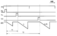
- FIG. 7 is a timing chart showing the operation of the reading circuit in the 1PD region of the image sensor 2.
- the floating diffusion FD is reset by turning on the transistor TrRES (high level at the reset signal Rst) at a predetermined timing according to the vertical synchronization signal HD. By turning on the transistor TrSEL after the reset, the reset voltage value is read out as a reset signal.
- the read reset signal is analog-to-digital converted (ADC) by the column ADC.
- the transistor TrL and the transistor TrR high level in the signal applied to TrL and TrR
- the charges of the photoelectric conversion element PDL and the photoelectric conversion element PDR are transferred to the floating diffusion FD.
- the transistor TrSEL By turning on the transistor TrSEL after the transfer, the voltage value of the electric charge accumulated in the floating diffusion FD is a pixel signal (a pixel signal of the electric charge generated by all the photoelectric conversion elements PDL and PDR provided in one pixel). Therefore, it is read as ALL).
- the read pixel signal ALL is analog-to-digital converted (ADC) by the column ADC.
- the reset signal and the pixel signal are read out in the same manner in synchronization with the vertical synchronization signal HD.
- CDS correlated double sampling
- FIG. 8 is a timing chart showing the operation of the reading circuit in the 2PD region of the image sensor 2 in the normal reading method.
- the transistor TrL the electric charge of the photoelectric conversion element PDL is transferred to the floating diffusion FD.
- the transistor TrSEL By turning on the transistor TrSEL after the transfer, the voltage value of the electric charge accumulated in the floating diffusion FD is read out as the divided pixel signal L.
- the read divided pixel signal L is analog-to-digital converted (ADC) by the column ADC.
- CDS correlated double sampling
- the floating diffusion FD is reset at a predetermined timing according to the vertical synchronization signal HD, the reset signal is read out, and ADC is performed.
- the transistor TrR the electric charge of the photoelectric conversion element PDR is transferred to the floating diffusion FD.
- the transistor TrSEL By turning on the transistor TrSEL after the transfer, the voltage value of the electric charge accumulated in the floating diffusion FD is read out as the divided pixel signal R.
- the read divided pixel signal R is analog-to-digital converted (ADC) by the column ADC.
- CDS correlated double sampling
- FIG. 9 is a timing chart showing the operation of the 2PD region reading circuit in the image sensor 2 in the additive reading method.
- the electric charge of the photoelectric conversion element PDL is transferred to the floating diffusion FD, the divided pixel signal L is read out, and ADC is performed.
- CDS correlated double sampling
- the electric charge of the photoelectric conversion element PDR is further transferred to the floating diffusion FD.
- the electric charge of the photoelectric conversion element PDL and the electric charge of the photoelectric conversion element PDR are accumulated in the floating diffusion FD.
- the voltage value of the electric charge accumulated in the floating diffusion FD is read out as a pixel signal (L + R).
- the read pixel signal (L + R) is analog-to-digital converted (ADC) by the column ADC.
- the acquisition time difference between the reset signal and the pixel signal (L + R) at this time is the CDS period T2 shown in FIG. Here, T2> T1.
- the pixel signal read from the 1PD area is described as ALL, but the pixel signal read from the 2PD area is described as (L + R). This is because, as will be described later, the pixel signal ALL and the pixel signal (L + R) are not always the same because the CDS period is different.
- the case of 2PD has been described above, but the same applies to the case of 4PD and the like.
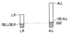
- FIG. 10 shows the divided pixel signals L and R read from the 2PD area and the reading from the 1PD area when the image sensor 2 operates in the normal reading method and the OB clamp circuit 2a of the image sensor 2 is one. It is a figure which shows the example of the OB level with the output pixel signal ALL.
- the divided pixel signal L generated by the photoelectric conversion element PDL and the divided pixel signal R generated by the photoelectric conversion element PDR are usually the photoelectric conversion element PDL and the photoelectric conversion element PDR. It becomes about half of the total pixel signal ALL generated in.
- the image sensor 2 generally sets the OB level of the image pickup signal to a predetermined target level (OB clamp level) (fixed value), and outputs a value obtained by adding a pixel signal proportional to the amount of incident light to the target level (OB clamp level) (fixed value).
- OB clamp level predetermined target level
- the signal level of the light-shielding pixel detected in the sensor clamp area SVOB which is a light-shielded area, is set to a fixed digital value (in the case of a 12-bit ADC, it is often set to, for example, 256 LSB).
- OB level processing (OB clamping processing) is performed so as to be.
- the dark current generated in the photoelectric conversion element PDL and the dark current generated in the photoelectric conversion element PDR are the photoelectric conversion element PDL and the photoelectric conversion element PDR.
- the level of the divided pixel signal is about half the level of the pixel signal, which is the same as the case of the signal generated by photoelectric conversion).
- the image sensor 2 has one OB clamp circuit 2a, and in the sensor clamp area SVOB, the 1PD area and the 2PD area that operates in the normal reading method (that is, L and R are read separately) are not distinguished from each other at the OB level.
- the average value of the dark current in the 1PD region and the 2PD region is detected as the OB level, and the detected OB is detected, although it may change depending on the time constant setting of the OB clamping process and the pattern of the 1PD region and the 2PD region.
- OB clamping is done at the level.
- the average value of the dark currents in the 1PD region and the 2PD region is processed to the OB clamp level OBC, so that the OB level OB_L of the photoelectric conversion element PDL and the photoelectric conversion element are processed after the OB clamp processing.
- the OB level OB_R of the PDR is lower than the OB clamp level OBC which is a fixed value, and the OB level OB_ALL caused by the total dark current generated in the photoelectric conversion element PDL and the photoelectric conversion element PDR is a fixed value OB clamp level. It will be higher than OBC.
- the difference between the OB level OB_L (or OB level OB_R) and the OB level OB_ALL is generated in both the dark current amount generated in the photoelectric conversion element PDL (or the photoelectric conversion element PDR) and the photoelectric conversion element PDL and the photoelectric conversion element PDR. Corresponds to the difference between the amount of dark current and the amount of dark current.
- the signal output from the effective region VRef of the image sensor 2 is above the signal level L and OB level OB_R in which the level of the photoelectric conversion amount (L-OB_L) by the photoelectric conversion element PDL is added to the OB level OB_L.
- the level of the photoelectric conversion amount by the photoelectric conversion element PDR (R-OB_R) is added to the signal level R, the level of the photoelectric conversion amount by the photoelectric conversion element PDL and the photoelectric conversion element PDR (ALL-OB_ALL) on the OB level OB_ALL. Is added to obtain the signal level ALL.
- the OB level (OB_L + OB_R) included in the pixel signal generated by adding the divided pixel signal L generated by the photoelectric conversion element PDL and the divided pixel signal R generated by the photoelectric conversion element PDR is generally set.
- the pixel signal Since it does not match the OB level OB_ALL, the pixel signal is deviated between the 1PD region and the 2PD region. Such a deviation of the signal value becomes conspicuous in a region where the photoelectric conversion amount is small (that is, a dark region).
- the PD mix circuit 22 adds the divided pixel signals R and L read from the 2PD area by the normal reading method while reducing the difference in OB level from the 1PD area to generate a pixel signal ((). 1) to (3) will be described.
- the PD mix circuit 22 converts the signal read from the photoelectric conversion element PDL in the square region (2PD region) set in the first vertical OB region VOB1 into the signal.
- the OB level OB_L is calculated based on the above
- the OB level OB_R is calculated based on the signal read from the photoelectric conversion element PDR in the square region set in the first vertical OB region VOB1.
- the PD mix circuit 22 calculates the OB level OB_ALL based on the signals read from the photoelectric conversion element PDL and the photoelectric conversion element PDR in the square region (1PD region) set in the second vertical OB region VOB2. do.
- n (two in this example, the same applies hereinafter) divided pixel signals L and R read from the normal pixel in the second read mode are added to generate an added normal pixel signal (L + R), and the second The n divided pixel signals OB_L and OB_R read from the OB pixel in the read mode of 2 are added to generate an added OB pixel signal (OB_L + OB_R), and the added OB pixel signal (OB_L + OB_R) is generated from the added normal pixel signal (L + R).
- the provisional OB subtraction pixel signal ⁇ (L-OB_L) + (R-OB_R) ⁇ is generated by subtraction, and the OB pixel signal OB_ALL read from the OB pixel in the first read mode is used as the provisional OB subtraction pixel signal ⁇ ((L-OB_L) + (R-OB_R) ⁇ . It is a process of adding to L-OB_L) + (R-OB_R) ⁇ to generate a calculation result Sum as pixel data. After that, the PD mix circuit 22 arranges the generated pixel data to generate a second pixel data array.
- addition processing for obtaining a pixel signal is performed, OB level OB_L included in the divided pixel signal L is removed (L-OB_L), and the processing is included in the divided pixel signal R. It can be rephrased as a process of removing the OB level OB_R (R-OB_R) and adding the OB level OB_ALL included in the pixel signal in the 1PD region.
- the OB level of the pixel signal read from the 2PD area and added up is converted to the OB level of the pixel signal read from the 1PD area. It can be adjusted accurately. Further, by the same processing as described above, the OB level of the pixel signal read from the 1PD area and added and obtained is accurately matched with the OB level of the pixel signal read from the 2PD area. That can also be achieved.
- the case of 2PD has been described above, but the same applies to the case of 4PD and the like.
- the PD mix circuit 22 includes an OB pixel signal generated or extracted from n signals read from the OB pixels in the second read mode, and an OB pixel signal read from the OB pixels in the first read mode. Is used to perform OB level correction processing on the normal pixel signal generated or extracted from the n signals read from the normal pixel in the second read mode.
- the OB level generally has a slightly different value for each Bayer color (Rr, Gr, Gb, Bb). Since the Bayer color is generated by the color filter, there is no difference in the actual pixel circuit itself even if the color is different. However, if the colors are different, the location where the pixel circuit is arranged is different, and the wiring route to the pixel circuit (wiring location, wiring length, etc.) is also different, so that the difference in OB level occurs due to these differences. It is.
- the PD mix circuit 22 performs the correction process for matching the OB level as described above by distinguishing the filter colors and performing the correction process separately for each pixel filter color (however, the OB level according to the filter color). This is not the case if the difference between the two can be ignored).
- FIG. 11 shows the divided pixel signals L and R read from the 2PD area and the reading from the 1PD area when the image sensor 2 operates in the normal reading method and the image sensor 2 has two OB clamp circuits 2a. It is a figure which shows the example of the OB level with the output pixel signal ALL.
- the first OB clamp circuit 2a is provided to detect the OB level OB_ALL in the 1PD region and perform OB clamp of the pixel signal read in the first read mode.
- the second OB clamp circuit 2a detects the OB level OB_L of the divided pixel signal L and the OB level OB_R of the divided pixel signal R, and performs OB clamping of n divided pixel signals read in the second read mode. It is provided for this purpose.
- the OB clamp level OBC2 of the divided pixel signals L and R in the 2PD region and the OB clamp level OBC1 of the pixel signal in the 1PD region become Should be at the same level. Then, as shown in the OB level comparison diagram on the left side of FIG. 11, it is expected that the difference between the OB level OB_L, OB_R in the 2PD region and the OB level OB_ALL in the 1PD region is absorbed.
- the gain is increased to amplify the photoelectric conversion amount by, for example, 10 times to several hundred times.
- a slight difference CE in the OB clamp level is amplified, which causes a deterioration in image quality.
- the PD mix circuit 22 performs a process of reducing the difference CE of the OB clamp levels of the two OB clamp circuits 2a when the divided pixel signals R and L are added to generate a pixel signal.
- the pixel signal generation processing performed here is the same as the above-mentioned (1) to (3), and is effective processing for the difference CE of the OB clamp level by the plurality of OB clamp circuits 2a.
- the PD mix circuit 22 performs the correction process for matching the OB level separately for each filter color of the pixels by distinguishing the filter colors, as described above.
- FIG. 12 shows one OB clamp circuit in which the pixel signal (L + R) read from the 2PD area and the pixel signal ALL read from the 1PD area of the image sensor 2 operating in the additive reading method are combined with each other. It is a figure which shows the example of the OB level at the time of OB clamp in 2a.
- the pixel signals other than the pixel signals (L + R) read from the 2PD region are also performed by the second OB clamp circuit 2a.
- One OB clamp for both the pixel signal (L + R) read from the 2PD area by the addition reading method of the second read mode and the pixel signal ALL read from the 1PD area in the first read mode When clamped in common in the circuit 2a, the OB levels are basically the same.
- the pixel signal generation processes (1) to (3) in this case are as follows.
- the floating diffusion FD is reset and then the pixel signal ALL is read.
- the time interval up to (CDS period T1) and the time interval from resetting the floating diffusion FD to reading out the pixel signal (L + R) (CDS period T2) are different in time length.
- the OB level OB_ (L + R) of the pixel signal (L + R) read from the 2PD area and the OB level OB_ALL of the pixel signal ALL read from the 1PD area become There may be slight differences. The processing when such a difference occurs will be described with reference to FIG.
- FIG. 13 shows an OB caused by a difference in the CDS period between the pixel signal (L + R) read from the 2PD area and the pixel signal ALL read from the 1PD area of the image sensor 2 operating in the additive reading method. It is a figure which shows the example which the level difference occurs.
- the OB level OB_ of the pixel signal (L + R) (L + R) and the OB level OB_ALL of the pixel signal ALL do not exactly match, and differ by a slight difference TE.
- the PD mix circuit 22 converts the signal read from the photoelectric conversion element PDL in the square region (2PD region) set in the first vertical OB region VOB1 into the signal.
- the OB level OB_L is calculated based on the above
- the OB level OB_ (L + R) is calculated based on the signals read from the photoelectric conversion element PDL and the photoelectric conversion element PDR in the square region set in the first vertical OB region VOB1. ..
- the PD mix circuit 22 calculates the OB level OB_ALL based on the signals read from the photoelectric conversion element PDL and the photoelectric conversion element PDR in the square region (1PD region) set in the second vertical OB region VOB2. do. That is, OB_ (L + R) from the 2PD region and OB_ALL from the 1PD region are distinguished.
- This process extracts the normal pixel signal (L + R) read from the normal pixel in the second read mode, extracts the OB pixel signal OB_ (L + R) read from the OB pixel in the second read mode, and extracts the normal pixel signal.
- the OB pixel signal OB_ (L + R) is subtracted from (L + R) to generate a provisional OB subtraction pixel signal ⁇ (L + R) -OB_ (L + R) ⁇ , and the OB pixel signal OB_ALL read from the OB pixel in the first read mode. Is added to the provisional OB subtraction pixel signal ⁇ (L + R) -OB_ (L + R) ⁇ to generate the calculation result Sum as pixel data.
- the PD mix circuit 22 arranges the generated pixel data to generate a second pixel data array. Further, it is also possible to achieve the process of accurately matching the OB pixel signal OB_ (L + R) read from the normal pixel in the second read mode by the same process as described above.
- the PD mix circuit 22 performs the correction process for matching the OB level separately for each filter color of the pixels by distinguishing the filter colors, as described above.
- the OB clamp of the pixel signal read in the first read mode and the second read mode are read.
- the OB clamp of one pixel signal may be performed by, for example, the first OB clamp circuit 2a.
- the second OB clamp circuit 2a may perform OB clamp of (n-1) signals read in the second read mode.
- the case of 2PD has been described above, but the same processing may be performed in the case of 4PD or the like.
- the PD mix circuit 22 performs the pixel signal generation processing as described above, and outputs image data (RAW image data) composed of only pixel signals (that is, not including divided pixel signals).
- the dark shading correction circuit 23 corresponding to PD mix processing performs dark shading correction on the RAW image data input from the PD mix circuit 22.
- the dark shading correction is a process for uniformly aligning the level fluctuation for each pixel that occurs in the plane of the image sensor 2 in the dark (when the incident light is blocked).
- the corrected image since the dark image is subtracted from the light image, the corrected image has more random noise than the light image before correction (or the dark image). It ends up.
- a plurality of dark images are acquired, the plurality of dark images are averaged to generate a light-shielded image for correction, and the generated correction light image is generated.
- the light-shielded image is stored in advance in the non-volatile storage portion of the memory 13. Then, the influence of random noise is reduced by subtracting the dark image previously held in the memory 13 with respect to the image input from the image sensor 2.
- the correction shading image is not limited to being non-volatilely held in the memory 13, and may be dynamically generated and used.
- a light-shielded image for correction is generated by acquiring and averaging a plurality of dark images before acquiring a light-time image, and temporarily holds the image in a volatile storage portion of a memory 13 in the image processing circuit 3. I will do it. Then, the correction shading image temporarily held in the image processing circuit 3 may be subtracted from the light image acquired thereafter.
- the PD mix processing is performed by the PD mix circuit 22.
- the pixel signal (L + R) obtained by adding the divided pixel signals R and L in the PD mix circuit 22 is doubled (more generally, pixels) by adding dark shading (more broadly, fixed pattern noise).
- k is a natural number (integer of 1 or more) and is a value of n or less.
- FIG. 14 is a diagram showing an example of dark shading in a normal exposure image, a high-speed video phase difference read exposure image (exposure image acquired in the high speed video phase difference read mode), and a light-shielding image for correction. Is.
- the amount of dark shading differs between the image portion corresponding to the 1PD region and the image portion corresponding to the 2PD region.
- FIG. 15 is a diagram for explaining a dark shading correction method for a high-speed video phase difference read exposure image in comparison with a dark shading correction method for a normal exposure image.
- the OB clamp level OBC which is the target level (fixed value) of the OB clamp.
- Dark shading which is a variation with respect to the above, is similarly included in the normal exposure image and the light-shielding image for correction.
- dark shading that fluctuates with respect to the OB clamp level OBC is included even in the lateral direction of the image.
- the OB clamp level OBC is subtracted from each pixel of the correction shading image to generate dark shading data, and the shading data is generated from each pixel data of the normal exposure image according to the pixel position.
- the dark shading data By subtracting the dark shading data, a normal exposure image corrected for dark shading can be obtained.
- dark shading correction is performed by the process shown in the high speed video phase difference read exposure image column of FIG.
- the dark shading correction circuit 23 corresponding to the PD mix processing converts the high-speed video phase difference read exposure image into an image portion corresponding to the 1PD region (each pixel data of the first pixel data array generated by the PD mix circuit 22). And the image portion corresponding to the 2PD region (each pixel data of the second pixel data array generated by the PD mix circuit 22).
- the dark shading correction circuit 23 corresponding to PD mix processing reads out a shading image for correction from the memory 13.
- the dark shading correction circuit 23 corresponding to PD mix processing subtracts the OB clamp level OBC from each pixel of the correction light-shielding image for the image portion corresponding to the 1PD region, as in the normal exposure image, to obtain dark shading data. Is generated, and dark shading correction is performed by subtracting dark shading data according to the pixel position from each pixel data of the image portion corresponding to the 1PD area.
- the dark shading correction circuit 23 corresponding to PD mix processing generates dark shading data by subtracting the OB clamp level OBC from each pixel of the correction shading image for the image portion corresponding to the 2PD area, and creates the dark shading data in the 2PD area.
- the correction method shown in FIG. 15 is more generally applied to the fixed pattern noise (FPN) (fixed pattern noise of vertical stripes, for example). Can be done.
- FPN fixed pattern noise
- the fixed pattern to be corrected is stored in the memory 13 or the like in advance, read from the memory 13 or the like at the time of correction, the image portion corresponding to the 1PD area is subtracted as it is, and the image portion corresponding to the kPD area is obtained. Multiplying by k and subtracting is the same as described above.
- the image sensor 2 since the image sensor 2 can read the image pickup signal related to the n divided pixel signals for each pixel row in the first read mode or the second read mode, the image sensor 2 takes an image. It is possible to obtain an image pickup device including an image sensor in which pixels are divided into a plurality of pixels, which can acquire phase difference information while suppressing a decrease in rate.
- the PD mix circuit 22 is a conventional circuit (described above) arranged after the PD mix circuit 22 in order to generate a first pixel data array and a second pixel data array having the same pixel data arrangement order.
- the conventional circuit can be used as it is without significantly changing the general processing circuit), and it is possible to significantly reduce the cost.
- the imaging signals of the normal pixel and the OB pixel are read out in the first read mode and the second read mode, and the PD mix circuit 22 generates or generates from n signals read from the OB pixel in the second read mode.
- the extracted OB pixel signal and the OB pixel signal read from the OB pixel in the first read mode it is usually generated or extracted from n signals read from the normal pixel in the second read mode. Since the pixel signal is subjected to the OB level correction processing, the OB level can be corrected with high accuracy.
- the added OB pixel signal obtained by adding n divided pixel signals is subtracted from the added normal pixel signal obtained by adding n divided pixel signals, and provisionally Since the OB subtraction pixel signal is generated and the OB pixel signal read from the OB pixel in the first read mode is added to the provisional OB subtraction pixel signal to generate pixel data, it is read in the second read mode.
- the OB level of the normal pixel signal generated from the n output signals can be matched with the OB level of the normal pixel signal read from the normal pixel in the first read mode with high accuracy.
- the image sensor 2 includes a plurality of OB clamp circuits 2a, the first OB clamp circuit 2a performs OB clamp of the pixel signal read in the first read mode, and the second OB clamp circuit 2a is the second.
- the OB clamp of the n divided pixel signals read in the read mode is performed, the OB level can be corrected with high accuracy by applying the same method.
- the normal pixel signal read from the normal pixel is extracted in the second read mode, and the OB pixel signal is read from the OB pixel in the second read mode.
- the OB pixel signal is subtracted from the normal pixel signal to generate a provisional OB subtraction pixel signal, and the OB pixel signal read from the OB pixel in the first read mode is added to the provisional OB subtraction pixel signal to obtain pixel data.
- the first OB clamp circuit 2a is read in the OB clamp of the pixel signal read in the first read mode and in the second read mode.
- OB clamp of one pixel signal is performed, and the second OB clamp circuit 2a performs OB clamp of (n-1) signals read in the second read mode. It is possible to align the OB levels of the pixel signals constituting the RAW image while performing the clamping process at high speed.
- the PD mix circuit 22 performs the OB level correction processing for each filter color by distinguishing the filter colors, so that even if the OB level differs depending on the filter color, the OB level correction with higher accuracy is performed. Can be done.
- an appropriate OB level correction can be performed on the image pickup signal output from the image sensor 2 having the Bayer array as the basic array.
- the dark shading correction circuit 23 corresponding to PD mix processing subtracts dark shading data according to the pixel position from each pixel data of the first pixel data array generated by the PD mix circuit 22, and the PD mix circuit 22 By subtracting the data obtained by multiplying the dark shading data according to the pixel position by n from each pixel data of the second pixel data array generated by, the dark shading correction in the high-speed video phase difference read mode is appropriately performed. It becomes possible to do. Further, if this correction method is applied to the fixed pattern noise, the fixed pattern noise correction can be appropriately performed.
- the memory 13 by configuring the memory 13 to store the correction shading image, it is not necessary to acquire the correction shading image every time the shooting is performed, and the shooting time can be shortened.
- circuits are not limited to electronic circuits configured as hardware, and are used in each circuit section of a processor having an integrated circuit (hardware) such as FPGA (Field Programmable Gate Array). It may be present, or it may be configured to perform the function of each circuit by causing a processor having hardware such as a CPU to execute the software.
- hardware such as FPGA (Field Programmable Gate Array).
- the present invention is not limited to the image pickup device, and may be an image pickup method, or a processing program for causing a computer to perform the same processing as the image pickup device. It may be a non-temporary recording medium or the like that can be read by a computer that records the processing program.
- the present invention is not limited to the above-described embodiment as it is, and at the implementation stage, the components can be modified and embodied within a range that does not deviate from the gist thereof.
- various aspects of the invention can be formed by an appropriate combination of the plurality of components disclosed in the above-described embodiment. For example, some components may be removed from all the components shown in the embodiments. In addition, components across different embodiments may be combined as appropriate. As described above, it goes without saying that various modifications and applications are possible within a range that does not deviate from the gist of the invention.
Abstract
An image capturing device according to the present invention is provided with an image sensor (2) having a plurality of pixels in which each pixel is divided n times, and an image processing circuit (3) which carries out image processing on an image capturing signal output by the image sensor (2). The image sensor (2) can read out pixel columns in a first read-out mode which generates a pixel signal from n divided pixel signals and reads the pixel signal out in one column, or a second read-out mode which generates n signals from n divided pixel signals and reads out the signals in n columns. The image processing circuit (3) processes the pixel signal which was read out in the first read out mode and the n signals which were read out in the second read-out mode, and generates image data in which pixel data is arranged in a prescribed order in each pixel column.
Description
本発明は、画素が複数に分割されたイメージセンサを備える撮像装置に関する。
The present invention relates to an imaging device including an image sensor in which pixels are divided into a plurality of pixels.
近年、像面位相差イメージセンサを搭載して、像面位相差AFを行うデジタルカメラ等の撮像装置が普及してきている。フォーカス位置を変更しながら取得した画像のコントラスト値のピークを探索する従来のコントラストAF方式に比べて、像面位相差AFはコントラスト値のピークを探索することなく、現在のフォーカス位置からフォーカスを合わせるためのフォーカスレンズの駆動方向と必要駆動量を取得することができるため、高速にフォーカスを合わせることができるという特徴がある。
In recent years, imaging devices such as digital cameras equipped with an image plane phase difference image sensor and performing image plane phase difference AF have become widespread. Compared to the conventional contrast AF method that searches for the peak of the contrast value of the acquired image while changing the focus position, the image plane phase difference AF focuses from the current focus position without searching for the peak of the contrast value. Since the drive direction and the required drive amount of the focus lens for the purpose can be acquired, there is a feature that the focus can be adjusted at high speed.
像面位相差イメージセンサは、瞳分割された光線を光電変換素子(光電変換素子の一例としてはフォトダイオード(PD)が挙げられ、以下では簡単のためにPDという)により光電変換して、位相差検知を可能とするものである。この像面位相差イメージセンサには、代表的な2つの方式があり、1つの方式は遮光式像面位相差イメージセンサ、他の1つの方式はPD分割方式像面位相差イメージセンサである。
In the image plane phase difference image sensor, the pupil-divided light beam is photoelectrically converted by a photoelectric conversion element (an example of the photoelectric conversion element is a photodiode (PD), which is hereinafter referred to as PD for simplicity). It enables phase difference detection. There are two typical methods for this image plane phase difference image sensor, one method is a light-shielding type image plane phase difference image sensor, and the other one is a PD division type image plane phase difference image sensor.
遮光式像面位相差イメージセンサは、画素内のマイクロレンズ下に配置されたPDへ入射する光線の一部を遮る遮光構造を備え、遮光構造の配置に応じて撮影レンズから入射する光線を瞳分割する方式のものである。
The light-shielding image plane phase difference image sensor has a light-shielding structure that blocks a part of the light rays incident on the PD arranged under the microlens in the pixel, and the light rays incident from the photographing lens are captured by the pupil according to the arrangement of the light-shielding structure. It is a division method.
一方、PD分割方式像面位相差イメージセンサは、遮光構造を備える代わりに、画素内におけるPDを分割することで、撮影レンズから入射する光線を瞳分割する方式のものである。PD分割方式における瞳分割の仕方は、PDの分割の仕方を変えることでなされる。
On the other hand, the PD division type image plane phase difference image sensor is a method in which the light rays incident from the photographing lens are divided into pupils by dividing the PD in the pixel instead of having a light-shielding structure. The pupil division method in the PD division method is performed by changing the PD division method.
例えば、日本国特開2016-105187号公報には、9分割されたPDの信号の、一部を加算平均することにより左瞳分割用の画素データを生成し、他の一部を加算平均することにより右瞳分割用の画素データを生成し、全てを加算平均することにより静止画用RAWデータの画素データを生成する技術が記載されている。
For example, in Japanese Patent Application Laid-Open No. 2016-105187, pixel data for left pupil division is generated by adding and averaging a part of the 9-divided PD signal, and the other part is added and averaged. This describes a technique for generating pixel data for right pupil division and generating pixel data for still image RAW data by adding and averaging all of them.
PD分割方式像面位相差イメージセンサでは、位相差検知するペア(例えば左右ペア、上下ペアなど)を1画素内で構成できるのに対して、遮光式像面位相差イメージセンサでは1画素内で構成できず複数画素を要するために、前者は後者よりもフォーカス検知精度を大幅に向上することができる。
In the PD division type image plane phase difference image sensor, the pair for detecting the phase difference (for example, left and right pair, upper and lower pair, etc.) can be configured within one pixel, whereas in the light-shielding image plane phase difference image sensor, within one pixel. Since it cannot be configured and requires a plurality of pixels, the former can significantly improve the focus detection accuracy as compared with the latter.
その一方で、非像面位相差のイメージセンサと比べて、遮光式像面位相差イメージセンサはPDの数が変わらないが、PD分割方式像面位相差イメージセンサは画素の分割数nに応じてPDの数がn倍になる。その結果、PD分割方式像面位相差イメージセンサは、遮光式像面位相差イメージセンサ(および非像面位相差のイメージセンサ)に対して、信号読出時間がn倍となって、撮像レートおよび位相差情報の取得レートが1/nになってしまう。
On the other hand, the number of PDs does not change in the light-shielding image plane phase difference image sensor as compared with the non-image plane phase difference image sensor, but the PD division type image plane phase difference image sensor corresponds to the number of pixel divisions n. The number of PDs increases n times. As a result, the PD division type image plane phase difference image sensor has n times the signal reading time as compared with the light-shielding type image plane phase difference image sensor (and the non-image plane phase difference image sensor), and the imaging rate and the imaging rate and the image sensor are increased. The acquisition rate of the phase difference information becomes 1 / n.
本発明は上記事情に鑑みてなされたものであり、撮像レートの低下を抑制しながら位相差情報も取得することができる、画素が複数に分割されたイメージセンサを備える撮像装置を提供することを目的としている。
The present invention has been made in view of the above circumstances, and provides an imaging device including an image sensor in which pixels are divided into a plurality of pixels, which can acquire phase difference information while suppressing a decrease in imaging rate. I am aiming.
本発明の一態様による撮像装置は、複数の画素が行方向および前記行方向に交差する方向に配列され、nを2以上の整数とすると、前記複数の画素は、それぞれ、1個のマイクロレンズと、n個の光電変換素子と、を備え、前記マイクロレンズからの光を前記n個の光電変換素子により光電変換して生成されるn個の分割画素信号、に係る撮像信号を出力するイメージセンサと、前記イメージセンサから出力される前記撮像信号を画像処理する画像処理回路と、を具備し、前記イメージセンサは、前記行方向に配列された複数の画素でなる画素行毎に、前記n個の分割画素信号に係る前記撮像信号を、第1の読出モードまたは第2の読出モードで読み出し可能であり、前記第1の読出モードは、前記n個の分割画素信号を加算して1個の画素信号を生成し、1画素行を1行で読み出すモードであり、前記第2の読出モードは、前記n個の分割画素信号からn個の信号を生成し、1画素行をn行で読み出すモードであり、前記画像処理回路は、前記第1の読出モードで読み出される画素行の画素信号と、前記第2の読出モードで読み出される画素行の前記n個の信号と、を処理して、画素行毎に画素データが所定の順序で配列された画像データを生成する。
In the imaging device according to one aspect of the present invention, when a plurality of pixels are arranged in a row direction and a direction in which the row direction intersects, and n is an integer of 2 or more, the plurality of pixels are each one microlens. An image that includes n photoelectric conversion elements and outputs an imaging signal related to n divided pixel signals generated by photoelectric conversion of light from the microlens by the n photoelectric conversion elements. The image sensor includes a sensor and an image processing circuit for image processing the imaging signal output from the image sensor, and the image sensor has the n for each pixel row composed of a plurality of pixels arranged in the row direction. The image pickup signal related to the divided pixel signals can be read out in the first read mode or the second read mode, and the first read mode is one by adding the n divided pixel signals. In the second read mode, n signals are generated from the n divided pixel signals and one pixel row is read in n rows. In the read mode, the image processing circuit processes the pixel signals of the pixel rows read in the first read mode and the n signals of the pixel rows read in the second read mode. , Generates image data in which pixel data is arranged in a predetermined order for each pixel row.
以下、図面を参照して本発明の実施の形態を説明する。
Hereinafter, embodiments of the present invention will be described with reference to the drawings.
図1から図15は本発明の一実施形態を示したものであり、図1は撮像装置の構成を示すブロック図である。
1 to 15 show an embodiment of the present invention, and FIG. 1 is a block diagram showing a configuration of an image pickup apparatus.
なお、図1には撮像装置が例えばデジタルカメラとして構成されている例を示すが、撮像装置はデジタルカメラに限定されるものではなく、デジタルビデオカメラ、撮影機能付き電話装置、電子内視鏡、撮影機能付き顕微鏡、撮影機能付き望遠鏡など、撮影機能を有する各種の装置の何れであっても構わない。
Although FIG. 1 shows an example in which the image pickup device is configured as, for example, a digital camera, the image pickup device is not limited to the digital camera, and the digital video camera, the telephone device with a shooting function, the electronic endoscope, and the like. Any of various devices having an imaging function, such as a microscope with an imaging function and a telescope with an imaging function, may be used.
この撮像装置は、図1に示すように、レンズ1と、イメージセンサ2と、画像処理回路3と、ディスプレイ4と、手振センサ6と、手振補正機構7と、フォーカス制御機構8と、カメラ操作デバイス9と、カメラコントローラ10と、を備えている。なお、図1には記録用メモリ5も記載されているが、この記録用メモリ5は撮像装置に対して着脱可能に構成されていても構わないために、撮像装置に固有の構成でなくてもよい。
As shown in FIG. 1, this image pickup apparatus includes a lens 1, an image sensor 2, an image processing circuit 3, a display 4, a camera shake sensor 6, a camera shake correction mechanism 7, a focus control mechanism 8, and the like. It includes a camera operating device 9 and a camera controller 10. Although the recording memory 5 is also shown in FIG. 1, the recording memory 5 may be configured to be detachable from the imaging device, and therefore is not unique to the imaging device. May be good.
レンズ1は、被写体の光学像をイメージセンサ2に結像する撮像光学系である。このレンズ1は、焦点位置(ピント位置)を調節してフォーカシングを行うためのフォーカスレンズを含む1枚以上のレンズと、通過する光束の範囲を制御するための絞りと、を備え、さらに、本実施形態においては手振補正機能も備えたものとなっている。
The lens 1 is an imaging optical system that forms an optical image of a subject on an image sensor 2. The lens 1 includes one or more lenses including a focus lens for adjusting the focus position (focus position) for focusing, and an aperture for controlling the range of the passing luminous flux. In the embodiment, the camera shake correction function is also provided.
なお、図示はしないが、例えばレンズ1とイメージセンサ2との間に、露光時間を制御するためのメカニカルシャッタをさらに備えているものとする。
Although not shown, it is assumed that, for example, a mechanical shutter for controlling the exposure time is further provided between the lens 1 and the image sensor 2.
イメージセンサ2は、レンズ1の撮影光軸の光路上に配置されていて、レンズ1により結像された被写体の光学像を光電変換して電気信号である撮像信号として出力する。
The image sensor 2 is arranged on the optical path of the photographing optical axis of the lens 1, and photoelectrically converts the optical image of the subject imaged by the lens 1 and outputs it as an imaging signal which is an electric signal.
イメージセンサ2は、複数の画素が行方向および行方向に交差する方向に配列されている。行方向に交差する方向は、一例としては行方向に直交する方向(列方向)が挙げられるが、これに限定されるものではなく、行方向に斜交する方向(例えば、いわゆるハニカム構造の配置)などであっても構わない。
The image sensor 2 is arranged in a row direction and a direction in which a plurality of pixels intersect in the row direction. An example of the direction intersecting the row direction is a direction orthogonal to the row direction (column direction), but the direction is not limited to this, and the direction diagonally intersects the row direction (for example, arrangement of a so-called honeycomb structure). ) Etc. may be used.
nを2以上の整数とすると、イメージセンサ2に設けられた複数の画素は、それぞれ、1個のマイクロレンズML(図3参照)と、n個の光電変換素子PD(図3参照)と、を備えている。なお、一般的な光学レンズは、光軸方向に沿って複数枚で構成されていることが通常である。従って、光軸方向に沿って複数枚で構成したマイクロレンズMLの場合にも、1個のマイクロレンズMLと数えることにする。
Assuming that n is an integer of 2 or more, the plurality of pixels provided in the image sensor 2 are each a microlens ML (see FIG. 3), n photoelectric conversion elements PD (see FIG. 3), and n. It has. It should be noted that a general optical lens is usually composed of a plurality of lenses along the optical axis direction. Therefore, even in the case of a microlens ML composed of a plurality of lenses along the optical axis direction, it is counted as one microlens ML.
そして、イメージセンサ2は、マイクロレンズMLからの光をn個の光電変換素子PDにより光電変換して生成されるn個の分割画素信号、に係る撮像信号を出力する。
Then, the image sensor 2 outputs an imaging signal related to n divided pixel signals generated by photoelectric conversion of light from the microlens ML by n photoelectric conversion elements PD.
ここに、n個の分割画素信号に係る撮像信号は、1画素がL(左)とR(右)に2分割されている場合を例に挙げれば、n個の分割画素信号自体(分割画素信号Lおよび分割画素信号R)、n個の分割画素信号を構成可能な信号(画素信号(L+R)および分割画素信号L)(または、画素信号(L+R)および分割画素信号R)n個の分割画素信号を加算して得られる画素信号(2PD領域からの画素信号(L+R)、1PD領域からの画素信号ALL)などである。
Here, as for the imaging signal related to the n divided pixel signals, for example, when one pixel is divided into L (left) and R (right), the n divided pixel signals themselves (divided pixels). Signal L and divided pixel signal R), signals that can configure n divided pixel signals (pixel signal (L + R) and divided pixel signal L) (or pixel signal (L + R) and divided pixel signal R) n divisions A pixel signal obtained by adding pixel signals (pixel signal (L + R) from 2PD region), pixel signal ALL from 1PD region, and the like.
イメージセンサ2は、1個のマイクロレンズMLに1つのフィルタ色が対応するように、複数のフィルタ色のカラーフィルタが所定の基本配列の繰り返しとして配置されたカラーイメージセンサとなっている。ただし、イメージセンサ2はカラーイメージセンサに限定されるものではなく、モノクロイメージセンサであっても構わない。
The image sensor 2 is a color image sensor in which color filters of a plurality of filter colors are arranged as repetitions of a predetermined basic arrangement so that one filter color corresponds to one microlens ML. However, the image sensor 2 is not limited to the color image sensor, and may be a monochrome image sensor.
イメージセンサ2の所定の基本配列は、例えば2×2画素のベイヤー配列(原色ベイヤー配列、補色ベイヤー配列など)が挙げられるが、これに限らず、6×6画素の基本配列などであっても構わない。本実施形態では、所定の基本配列が原色ベイヤー配列である場合を説明する。
The predetermined basic array of the image sensor 2 is, for example, a Bayer array of 2 × 2 pixels (primary color Bayer array, complementary color Bayer array, etc.), but the present invention is not limited to this, and a basic array of 6 × 6 pixels may be used. I do not care. In the present embodiment, the case where the predetermined basic arrangement is the primary color Bayer arrangement will be described.
こうして、イメージセンサ2は、画素が複数の分割画素に分割された、いわゆるPD分割方式像面位相差イメージセンサとなっている。
In this way, the image sensor 2 is a so-called PD division type image plane phase difference image sensor in which the pixels are divided into a plurality of divided pixels.
ここで、図3は、イメージセンサ2における、2分割および4分割の画素分割構成と読出回路との例を示す図表である。
Here, FIG. 3 is a chart showing an example of a 2-division and 4-division pixel division configuration and a read circuit in the image sensor 2.
原色ベイヤー配列は、縦2×横2画素を基本配列として、基本配列を行方向および列方向に周期的に繰り返したものとなっている。原色ベイヤー配列の基本配列は、対角位置に緑色フィルタGr,Gbを配置し、緑色フィルタGrと同一行に赤色フィルタRrを、緑色フィルタGbと同一行に青色フィルタBbを、それぞれ配置したものである。
The primary color Bayer array is a basic array of 2 vertical x 2 horizontal pixels, and the basic array is periodically repeated in the row direction and the column direction. In the basic array of the primary color Bayer array, the green filters Gr and Gb are arranged diagonally, the red filter Rr is arranged in the same row as the green filter Gr, and the blue filter Bb is arranged in the same row as the green filter Gb. be.
ここに、緑色フィルタGrと緑色フィルタGbは分光特性が同一であるが、赤色フィルタRrと青色フィルタBbとの何れと同一行であるかに応じて区別している。なお、左(L)右(R)のRと区別するために、フィルタ色の赤はRrと記載しており、青も同様にBbと記載している。
Here, the green filter Gr and the green filter Gb have the same spectral characteristics, but they are distinguished according to which of the red filter Rr and the blue filter Bb has the same line. In order to distinguish it from R on the left (L) and right (R), the filter color red is described as Rr, and blue is also described as Bb.
そして、1個の画素には、4つのフィルタ色Rr,Gr,Gb,Bbの内の何れか1つのフィルタ色のカラーフィルタと、1個のマイクロレンズMLと、が含まれている。ここに、非像面位相差のイメージセンサ(または、遮光式像面位相差イメージセンサ)の場合には、1個の画素に1個の光電変換素子PDが対応する構成となるが、本実施形態の、PD分割方式像面位相差イメージセンサであるイメージセンサ2は、画素の分割数nに応じたn個の光電変換素子PDが1個の画素に含まれる構成となっている。
Then, one pixel includes a color filter of any one of the four filter colors Rr, Gr, Gb, and Bb, and one microlens ML. Here, in the case of a non-image plane phase difference image sensor (or a light-shielding image plane phase difference image sensor), one photoelectric conversion element PD corresponds to one pixel. The image sensor 2, which is a PD division type image plane phase difference image sensor, has a configuration in which n photoelectric conversion elements PD corresponding to the number of pixel divisions n are included in one pixel.
また、イメージセンサ2に設けられている複数の画素は、遮光膜等が形成されておらず遮光されていない通常画素と、画素の受光部上の全面に遮光膜等が形成されていて遮光された画素であるOB(オプティカルブラック(Optical Black):光学黒)画素と、を含む。通常画素およびOB画素の配置例については、後で図6を参照して説明する。
Further, the plurality of pixels provided in the image sensor 2 are light-shielded by forming a light-shielding film or the like on the entire surface of the normal pixel and the light-receiving portion of the pixel. OB (Optical Black: optical black) pixel, which is a pixel, is included. An example of arranging the normal pixels and the OB pixels will be described later with reference to FIG.
図3の第1欄は1個の画素が右(R)左(L)に2分割された例を示している。なお、図3において、表の横並びを上から下に向かって順に第1欄~第3欄と呼んでいる。
The first column of FIG. 3 shows an example in which one pixel is divided into two parts, right (R) and left (L). In FIG. 3, the side-by-side arrangement of the tables is referred to as columns 1 to 3 in order from top to bottom.
ここに、1個のマイクロレンズMLに対するn個の光電変換素子PDの配置を、分割配置と呼ぶことにする。このとき、第1欄に示す分割配置は、左(L)および右(R)の2種類(n=2)である。このRL分割配置は、横方向の位相差検知(いわゆる縦線検知)に適している。
Here, the arrangement of n photoelectric conversion elements PD with respect to one microlens ML is referred to as a divided arrangement. At this time, the divided arrangement shown in the first column is two types (n = 2) of left (L) and right (R). This RL division arrangement is suitable for horizontal phase difference detection (so-called vertical line detection).
そして、各フィルタ色Rr,Gr,Gb,Bbの画素に対して、2つの分割配置の光電変換素子PD、すなわち、左側の光電変換素子PDL,右側の光電変換素子PDRがそれぞれ設けられている。各光電変換素子PDL,PDRは、例えばフォトダイオードとして構成され、入射光を光電変換して電荷を発生させる。
Then, for the pixels of each filter color Rr, Gr, Gb, Bb, two divided photoelectric conversion element PDs, that is, a photoelectric conversion element PDL on the left side and a photoelectric conversion element PDR on the right side are provided, respectively. Each photoelectric conversion element PDL and PDR is configured as, for example, a photodiode, and photoelectrically converts incident light to generate an electric charge.
各光電変換素子PDL,PDRは、読出スイッチとして機能するトランジスタTrL,TrRをそれぞれ経由して、フローティングディフュージョンFDに接続されている。
Each photoelectric conversion element PDL and PDR are connected to a floating diffusion FD via transistors TrL and TrR that function as read switches, respectively.
このような構成において、トランジスタTrL,TrRの1つ以上をオンすれば、オンにされたトランジスタTrに接続されている光電変換素子PDの電荷がフローティングディフュージョンFDへ転送される。
In such a configuration, if one or more of the transistors TrL and TrR are turned on, the electric charge of the photoelectric conversion element PD connected to the turned-on transistor Tr is transferred to the floating diffusion FD.
従って、トランジスタTrL,TrRの何れか1つだけをオンすれば、光電変換素子PDL,PDRの内の何れか1つだけの電荷がフローティングディフュージョンFDへ転送され、後述するように、分割画素信号Lまたは分割画素信号Rを読み出すことができる。
Therefore, if only one of the transistors TrL and TrR is turned on, the charge of only one of the photoelectric conversion elements PDL and PDR is transferred to the floating diffusion FD, and the divided pixel signal L is described later. Alternatively, the divided pixel signal R can be read out.
また、トランジスタTrL,TrRの2つをオンすれば、光電変換素子PDL,PDRの電荷がフローティングディフュージョンFDへ転送され、つまり、2個の光電変換素子PDL,PDRの電荷が加算されて、通常(L+R)の画素信号を読み出すことができる。
Further, when the two transistors TrL and TrR are turned on, the charges of the photoelectric conversion elements PDL and PDR are transferred to the floating diffusion FD, that is, the charges of the two photoelectric conversion elements PDL and PDR are added to each other, which is usually ( The pixel signal of L + R) can be read out.
フローティングディフュージョンFDおよびトランジスタTrL,TrRは、リセットスイッチとして機能するトランジスタTrRESを経由して、電源電圧VDDに接続されている。トランジスタTrRESをオンすることで、フローティングディフュージョンFDがリセットされる。このときさらに、トランジスタTrL,TrRを同時にオンすれば、各光電変換素子PDL,PDRもリセットされる。
The floating diffusion FD and the transistors TrL and TrR are connected to the power supply voltage VDD via the transistor TrRES that functions as a reset switch. By turning on the transistor TrRES, the floating diffusion FD is reset. At this time, if the transistors TrL and TrR are turned on at the same time, the photoelectric conversion elements PDL and PDR are also reset.
フローティングディフュージョンFDは、トランジスタTrAMPとトランジスタTrSELとを経由して、垂直信号線VSLに接続されている。ここに、トランジスタTrAMPは、電源電圧VDDに接続されトランジスタTrSELを経由し図示していない定電流回路と接続されて増幅回路として機能し、トランジスタTrSELは、選択スイッチとして機能する。
The floating diffusion FD is connected to the vertical signal line VSL via the transistor TrAMP and the transistor TrSEL. Here, the transistor TrAMP is connected to the power supply voltage VDD and is connected to a constant current circuit (not shown) via the transistor TrSEL to function as an amplifier circuit, and the transistor TrSEL functions as a selection switch.
そして、トランジスタTrSELをオンすることで、フローティングディフュージョンFDの電圧値がトランジスタTrAMPにより増幅されて、垂直信号線VSLから読み出されるようになっている。
Then, by turning on the transistor TrSEL, the voltage value of the floating diffusion FD is amplified by the transistor TrAMP and read from the vertical signal line VSL.
次に、図3の第2欄は1個の画素が上(U)下(D)に2分割された例を示している。
Next, the second column of FIG. 3 shows an example in which one pixel is divided into upper (U) and lower (D).
すなわち、第2欄に示す分割配置は、上(U)および下(D)の2種類(n=2)である。このUD分割配置は、縦方向の位相差検知(いわゆる横線検知)に適している。
That is, there are two types (n = 2) of the divided arrangement shown in the second column, upper (U) and lower (D). This UD split arrangement is suitable for vertical phase difference detection (so-called horizontal line detection).
そして、各フィルタ色Rr,Gr,Gb,Bbの画素に対して、2つの分割配置の光電変換素子PD、すなわち、上側の光電変換素子PDU,下側の光電変換素子PDDがそれぞれ設けられている。各光電変換素子PDU,PDDは、例えばフォトダイオードとして構成され、入射光を光電変換して電荷を発生させる。
Then, for the pixels of each filter color Rr, Gr, Gb, Bb, two dividedly arranged photoelectric conversion element PDs, that is, an upper photoelectric conversion element PDU and a lower photoelectric conversion element PDD are provided, respectively. .. Each photoelectric conversion element PDU and PDD is configured as, for example, a photodiode, and photoelectrically converts incident light to generate an electric charge.
なお、読出回路は、LRがUDになった点を除いて、RL2分割の場合と同様である。
The read circuit is the same as in the case of RL2 division, except that the LR is UD.
そして、トランジスタTrU,TrDの何れか1つだけをオンすれば、U分割画素信号またはD分割画素信号を読み出すことができる。
Then, if only one of the transistors TrU and TrD is turned on, the U-divided pixel signal or the D-divided pixel signal can be read out.
一方、トランジスタTrU,TrDの2つをオンすれば、2個の光電変換素子PDU,PDDの電荷が加算されて、通常(U+D)の画素信号を読み出すことができる。
On the other hand, if two transistors TrU and TrD are turned on, the charges of the two photoelectric conversion elements PDU and PDD are added, and a normal (U + D) pixel signal can be read out.
続いて、図3の第3欄は1個の画素が右(R)左(L)上(U)下(D)に4分割された例を示している。
Subsequently, the third column of FIG. 3 shows an example in which one pixel is divided into four parts, right (R), left (L), upper (U), and lower (D).
第3欄に示す分割配置は、左上(LU),右上(RU),左下(LD),右下(RD)の4種類(n=4)である。この4分割配置は、横方向の位相差検知(いわゆる縦線検知)と、縦方向の位相差検知(いわゆる横線検知)と、の何れにも適している。
There are four types (n = 4) of the divided arrangements shown in the third column: upper left (LU), upper right (RU), lower left (LD), and lower right (RD). This 4-split arrangement is suitable for both horizontal phase difference detection (so-called vertical line detection) and vertical phase difference detection (so-called horizontal line detection).
そして、各フィルタ色Rr,Gr,Gb,Bbの画素に対して、4つの分割配置の光電変換素子PD、すなわち、左上側の光電変換素子PDLU,右上側の光電変換素子PDRU,左下側の光電変換素子PDLD,右下側の光電変換素子PDRDがそれぞれ設けられている。各光電変換素子PDLU,PDRU,PDLD,PDRDは、例えばフォトダイオードとして構成され、入射光を光電変換して電荷を発生させる。
Then, for the pixels of each filter color Rr, Gr, Gb, Bb, the photoelectric conversion element PD having four divided arrangements, that is, the photoelectric conversion element PDLU on the upper left side, the photoelectric conversion element PDRU on the upper right side, and the photoelectric on the lower left side. A conversion element PDLD and a photoelectric conversion element PDRD on the lower right side are provided, respectively. Each photoelectric conversion element PDLU, PDRU, PDLD, PDRD is configured as, for example, a photodiode, and photoelectrically converts incident light to generate an electric charge.
各光電変換素子PDLU,PDRU,PDLD,PDRDは、読出スイッチとして機能するトランジスタTrLU,TrRU,TrLD,TrRDをそれぞれ経由して、フローティングディフュージョンFDに接続されている。
Each photoelectric conversion element PDLU, PDRU, PDLD, PDRD is connected to a floating diffusion FD via transistors TrLU, TrRU, TrLD, and TrRD that function as read switches, respectively.
このような構成において、トランジスタTrLU,TrRU,TrLD,TrRDの1つ以上をオンすれば、オンにされたトランジスタTrに接続されている光電変換素子PDの電荷がフローティングディフュージョンFDへ転送される。
In such a configuration, if one or more of the transistors TrLU, TrRU, TrLD, and TrRD are turned on, the electric charge of the photoelectric conversion element PD connected to the turned-on transistor Tr is transferred to the floating diffusion FD.
従って、トランジスタTrLU,TrRU,TrLD,TrRDの内の1つだけをオンすれば、光電変換素子PDLU,PDRU,PDLD,PDRDの内の1つだけの電荷がフローティングディフュージョンFDへ転送され、LU分割画素信号、RU分割画素信号、LD分割画素信号、またはRD分割画素信号として読み出すことができる。
Therefore, if only one of the transistors TrLU, TrRU, TrLD, and TrRD is turned on, the charge of only one of the photoelectric conversion elements PDLU, PDRU, PDLD, and PDRD is transferred to the floating diffusion FD, and the LU division pixel. It can be read as a signal, a RU-divided pixel signal, an LD-divided pixel signal, or an RD-divided pixel signal.
また、トランジスタTrLU,TrRU,TrLD,TrRDの内の2つ以上をオンすれば、光電変換素子PDLU,PDRU,PDLD,PDRDの内の2つ以上の電荷がフローティングディフュージョンFDへ転送され、つまり、2個以上の光電変換素子PDの電荷が加算されて読み出すことができる。
Further, when two or more of the transistors TrLU, TrRU, TrLD, and TrRD are turned on, two or more charges of the photoelectric conversion elements PDLU, PDRU, PDLD, and PDRD are transferred to the floating diffusion FD, that is, 2 The charges of one or more photoelectric conversion elements PD can be added and read out.
従って、例えばUD加算を行うことで、L(LU+LD)分割画素信号、R(RU+RD)分割画素信号を読み出すことができる。この読み出し方法を採用する場合には、1個の画素がRLに2分割されている(n=2である)ものとして取り扱うことができる。
Therefore, for example, by performing UD addition, the L (LU + LD) divided pixel signal and the R (RU + RD) divided pixel signal can be read out. When this reading method is adopted, it can be treated as if one pixel is divided into RL (n = 2).
また例えばRL加算を行うことで、U(LU+RU)分割画素信号、D(LD+RD)分割画素信号を読み出すことができる。この読み出し方法を採用する場合には、1個の画素がUDに2分割されている(n=2である)ものとして取り扱うことができる。
Further, for example, by performing RL addition, a U (LU + RU) divided pixel signal and a D (LD + RD) divided pixel signal can be read out. When this reading method is adopted, it can be treated as if one pixel is divided into two by UD (n = 2).
さらに例えばRLUD加算を行うことで、通常(LU+RU+LD+RD)の画素信号を読み出すことができる。
Further, for example, by performing RLUD addition, a normal (LU + RU + LD + RD) pixel signal can be read out.
加えて、RLUD4分割の画素の内の3つを加算(具体的に、LU+RU+LD、LU+RU+RD、LU+LD+RD、RU+LD+RD)した分割画素信号を読み出すことも可能となっている。
In addition, it is also possible to read a divided pixel signal obtained by adding three of the RLUD4 divided pixels (specifically, LU + RU + LD, LU + RU + RD, LU + LD + RD, RU + LD + RD).
フローティングディフュージョンFDおよびトランジスタTrLU,TrRU,TrLD,TrRDは、リセットスイッチとして機能するトランジスタTrRESを経由して、電源電圧VDDに接続されている。トランジスタTrRESをオンすることで、フローティングディフュージョンFDがリセットされる。このときさらに、トランジスタTrLU,TrRU,TrLD,TrRDを同時にオンすれば、各光電変換素子PDLU,PDRU,PDLD,PDRDもリセットされる。
The floating diffusion FD and the transistors TrLU, TrRU, TrLD, and TrRD are connected to the power supply voltage VDD via the transistor TrRES that functions as a reset switch. By turning on the transistor TrRES, the floating diffusion FD is reset. At this time, if the transistors TrLU, TrRU, TrLD, and TrRD are turned on at the same time, the photoelectric conversion elements PDLU, PDRU, PDLD, and PDRD are also reset.
フローティングディフュージョンFDは、電源電圧VDDに接続されトランジスタTrSELを経由し図示していない定電流回路と接続されて増幅回路として機能するトランジスタTrAMPと、選択スイッチとして機能するトランジスタTrSELと、を経由して垂直信号線VSLに接続されている。
The floating diffusion FD is vertical via a transistor TrAMP which is connected to a power supply voltage VDD and is connected to a constant current circuit (not shown) via a transistor TrSEL to function as an amplifier circuit and a transistor TrSEL which functions as a selection switch. It is connected to the signal line VSL.
そして、トランジスタTrSELをオンすることで、フローティングディフュージョンFDの電圧値がトランジスタTrAMPにより増幅されて、垂直信号線VSLから読み出されるようになっている。
Then, by turning on the transistor TrSEL, the voltage value of the floating diffusion FD is amplified by the transistor TrAMP and read from the vertical signal line VSL.
このようなPD分割方式像面位相差イメージセンサから、画素内の全ての分割画素を加算して画素信号を生成し読み出す(適宜、映像読出モードという)と、画素分割されていない通常のイメージセンサから画素信号を読み出す場合と同様の読出時間で読み出すことができるが、位相差情報を得ることができない。
From such a PD division type image plane phase difference image sensor, when all the divided pixels in the pixel are added to generate and read a pixel signal (appropriately referred to as a video read mode), a normal image sensor without pixel division is used. It can be read with the same read time as when the pixel signal is read from, but phase difference information cannot be obtained.
一方、PD分割方式像面位相差イメージセンサから全ての分割画素を読み出す(適宜、全位相差読出モードという)と、分割画素を加算して画素信号を生成し読み出す場合に比べて、2分割の場合には約2倍の読出時間が、4分割の場合には約4倍の読出時間がかかるために、撮像レートが低下してしまう。
On the other hand, when all the divided pixels are read from the PD division method image plane phase difference image sensor (appropriately referred to as all phase difference read mode), the pixel signal is generated and read by adding the divided pixels, and the two divisions are performed. In this case, the reading time is about twice as long, and in the case of four divisions, the reading time is about four times as long, so that the imaging rate is lowered.
そこで、本実施形態のイメージセンサ2は、行方向に配列された複数の画素でなる画素行毎に、n個の分割画素信号に係る撮像信号を、第1の読出モードまたは第2の読出モードで読み出す(ある画素行を第1の読出モードで読み出し、他の画素行を第2の読出モードで読み出す)ことが可能となっている。このような読出モードを、適宜、高速映像位相差読出モードと呼ぶことにする。
Therefore, the image sensor 2 of the present embodiment reads the imaging signal related to n divided pixel signals in the first read mode or the second read mode for each pixel row composed of a plurality of pixels arranged in the row direction. (A certain pixel row is read in the first read mode, and another pixel row is read in the second read mode). Such a read mode will be appropriately referred to as a high-speed video phase difference read mode.
この高速映像位相差読出モードにおいて、イメージセンサ2は、通常画素の撮像信号を、第1の読出モードおよび第2の読出モードで読み出す(ある通常画素行を第1の読出モードで読み出し、他の通常画素行を第2の読出モードで読み出す)とともに、OB画素の撮像信号を、第1の読出モードおよび第2の読出モードで読み出す(あるOB画素行を第1の読出モードで読み出し、他のOB画素行を第2の読出モードで読み出す)。
In this high-speed video phase difference read mode, the image sensor 2 reads the image pickup signal of the normal pixel in the first read mode and the second read mode (a certain normal pixel line is read in the first read mode, and the other is read. Along with reading the normal pixel line in the second read mode), the image pickup signal of the OB pixel is read in the first read mode and the second read mode (a certain OB pixel line is read in the first read mode, and the other is read. Read the OB pixel line in the second read mode).
ここに、第1の読出モードは、n個の分割画素信号を加算して1個の画素信号を生成し、1画素行を1行で読み出すモードである。第1の読出モードでは、1個の画素が1個の光電変換素子PDのみで構成されている(つまり分割されていない)状態と同等の画素信号が出力されることから、適宜、「1PD」と記載する。
Here, the first read mode is a mode in which n divided pixel signals are added to generate one pixel signal, and one pixel line is read by one line. In the first read mode, a pixel signal equivalent to a state in which one pixel is composed of only one photoelectric conversion element PD (that is, not divided) is output. Therefore, "1PD" is appropriately used. It is described as.
また、第2の読出モードは、n個の分割画素信号からn個の信号を生成し、1画素行をn行、または、それより少ない自然数(1以上の整数)行で読み出すモードである。この第2の読出モードには、後述するように、通常読み出し方式と加算読み出し方式の2つがあるが、何れの方式で読み出したとしても、n個、または、それより少ない自然数(1以上の整数)の信号を出力することから、適宜、その読み出し行数を用いた「kPD」ここで、kは自然数(1以上の整数)でn以下の値(2分割の場合でk=nの場合には「2PD」)と記載する。
The second read mode is a mode in which n signals are generated from n divided pixel signals and one pixel line is read with n lines or less natural number (integer of 1 or more) lines. As will be described later, there are two reading modes, a normal reading method and an additive reading method. Regardless of which method is used, n or less natural numbers (integers of 1 or more) are used. ) Is output, so the number of read lines is used as appropriate. Here, k is a natural number (integer of 1 or more) and a value of n or less (when k = n in the case of two divisions). Is described as "2PD").
このように第1の読出モードで読み出す画素行と第2の読出モードで読み出す画素行との両方を設けることより、撮像レートの低下を抑制しながら、位相差情報も取得することが可能となる。
By providing both the pixel rows read in the first read mode and the pixel rows read in the second read mode in this way, it is possible to acquire phase difference information while suppressing a decrease in the imaging rate. ..
なお、本実施形態のイメージセンサ2は、上述した映像読出モードおよび全位相差読出モードでも動作可能であるが、以下では、高速映像位相差読出モードで動作する場合について説明する。
The image sensor 2 of the present embodiment can also operate in the video read mode and the all-phase difference read mode described above, but the case of operating in the high-speed video phase difference read mode will be described below.
読出回路から読み出された撮像信号は、イメージセンサ2内に設けられた図示しない列並列型A/D変換器(いわゆるカラムADC)によりデジタル信号に変換され、イメージセンサ2内に設けられたOBクランプ回路2aによりOBレベルを所定の目標レベル(OBクランプレベル)(固定値)に設定される。ここに、カラムADCおよびOBクランプ回路2aは、1つずつ設けられているに限らず、読出速度を向上するため等により複数設けられていることもある。
The image pickup signal read from the read circuit is converted into a digital signal by a column-parallel A / D converter (so-called column ADC) provided in the image sensor 2 (not shown), and the OB provided in the image sensor 2 The OB level is set to a predetermined target level (OB clamp level) (fixed value) by the clamp circuit 2a. Here, the column ADC and the OB clamp circuit 2a are not limited to be provided one by one, but may be provided in plurality in order to improve the reading speed or the like.
画像処理回路3は、イメージセンサ2から出力される撮像信号(n個の光電変換素子PDにより生成されたn個の分割画素信号に係る、撮像信号)を入力して、入力した信号に各種の画像処理を行い、表示用もしくは記録用の画像信号を生成するものである。
The image processing circuit 3 inputs an imaging signal (an imaging signal related to n divided pixel signals generated by the n photoelectric conversion elements PD) output from the image sensor 2, and various types of input signals are input. Image processing is performed to generate an image signal for display or recording.
ディスプレイ4は、画像処理回路3により表示用に画像処理された信号に基づき、画像を表示する表示デバイスである。このディスプレイ4は、ライブビュー表示、撮影後の静止画像のレックビュー表示、記録済みの静止画像の再生表示、動画録画中表示、記録済みの動画像の再生表示等を行うとともに、この撮像装置に係る各種の情報等も表示するようになっている。
The display 4 is a display device that displays an image based on a signal that has been image-processed for display by the image processing circuit 3. The display 4 displays a live view, a rec-view display of a still image after shooting, a playback display of a recorded still image, a display during video recording, a playback display of a recorded moving image, and the like, and is used on the imaging device. Various kinds of related information are also displayed.
記録用メモリ5は、画像処理回路3により記録用に画像処理された信号(静止画像信号、動画像信号など)を保存するためのものであり、例えば撮像装置に着脱可能なメモリカード、もしくは撮像装置の内部に設けられている不揮発性メモリ等により構成されている。
The recording memory 5 is for storing signals (still image signals, moving image signals, etc.) image-processed for recording by the image processing circuit 3, and is, for example, a memory card that can be attached to and detached from an image pickup device, or an image pickup. It is composed of a non-volatile memory or the like provided inside the device.
手振センサ6は、加速度センサや角速度センサ等を有して構成され、撮像装置の手振れを検出してカメラコントローラ10へ出力するセンシングデバイスである。
The hand shake sensor 6 is a sensing device that includes an acceleration sensor, an angular velocity sensor, and the like, detects the hand shake of the image pickup device, and outputs the camera shake to the camera controller 10.
手振補正機構7は、カメラコントローラ10の制御に基づいて、手振センサ6により検出された手振れを相殺するようにレンズ1とイメージセンサ2との少なくとも一方をアクチュエータ等により移動し、イメージセンサ2に結像される光学的な被写体像に手振れの影響が生じるのを軽減するメカニカル機構である。
Based on the control of the camera controller 10, the camera shake correction mechanism 7 moves at least one of the lens 1 and the image sensor 2 by an actuator or the like so as to cancel the camera shake detected by the hand shake sensor 6, and the image sensor 2 It is a mechanical mechanism that reduces the influence of camera shake on the optical subject image that is imaged on the lens.
フォーカス制御機構8は、カメラコントローラ10の制御に基づいて、レンズ1に含まれるフォーカスレンズを駆動し、イメージセンサ2に結像される被写体像が合焦に至るようにするメカニカル機構である。また、フォーカス制御機構8は、レンズ位置などのレンズ駆動情報をカメラコントローラ10へ出力するようになっている。
The focus control mechanism 8 is a mechanical mechanism that drives the focus lens included in the lens 1 based on the control of the camera controller 10 so that the subject image formed on the image sensor 2 comes into focus. Further, the focus control mechanism 8 outputs lens drive information such as a lens position to the camera controller 10.
カメラ操作デバイス9は、撮像装置に対する各種の操作を行うための入力デバイスである。カメラ操作デバイス9には、例えば、撮像装置の電源をオン/オフするための電源スイッチ、静止画撮影または動画撮影などを指示入力するためのレリーズボタン、静止画撮影モード、動画撮影モード、ライブビューモード、静止画/動画再生モードなどを設定するためのモードボタン、記録するファイルの種類(JPEG画像ファイル、RAW画像ファイル、もしくはこれらの組み合わせ等)を設定するための操作ボタン、などの操作部材が含まれている。
The camera operation device 9 is an input device for performing various operations on the image pickup device. The camera operating device 9 has, for example, a power switch for turning on / off the power of the image pickup device, a release button for instructing and inputting still image shooting or movie shooting, a still image shooting mode, a movie shooting mode, and a live view. Operation members such as mode buttons for setting the mode, still image / video playback mode, and operation buttons for setting the type of file to be recorded (JPEG image file, RAW image file, or a combination thereof, etc.) include.
カメラコントローラ10は、画像処理回路3からの情報(後述するように、露光レベル、コントラスト、位相差などの情報を含む)、手振センサ6からの手振情報、フォーカス制御機構8からのレンズ駆動情報、カメラ操作デバイス9からの入力などに基づいて、レンズ1、イメージセンサ2、画像処理回路3、記録用メモリ5、手振補正機構7、フォーカス制御機構8等を含むこの撮像装置全体を制御するものである。
The camera controller 10 includes information from the image processing circuit 3 (including information such as exposure level, contrast, and phase difference as described later), camera shake information from the hand shake sensor 6, and lens drive from the focus control mechanism 8. Based on information, input from the camera operating device 9, etc., the entire image pickup device including the lens 1, the image sensor 2, the image processing circuit 3, the recording memory 5, the camera shake correction mechanism 7, the focus control mechanism 8, etc. is controlled. Is what you do.
例えば、カメラコントローラ10は、イメージセンサ2を駆動制御して撮像を行わせる。また、カメラコントローラ10は、露光レベルの情報に基づいて、レンズ1の絞りを制御するようになっている。
For example, the camera controller 10 drives and controls the image sensor 2 to perform imaging. Further, the camera controller 10 controls the aperture of the lens 1 based on the exposure level information.
さらに、カメラコントローラ10は、コントラストまたは位相差の情報に基づいてフォーカス制御機構8を制御し、レンズ1のフォーカスレンズを駆動させて、コントラストAFまたは位相差AFによるオートフォーカスを行わせる。
Further, the camera controller 10 controls the focus control mechanism 8 based on the contrast or phase difference information, drives the focus lens of the lens 1, and causes autofocus by contrast AF or phase difference AF.
次に、図2は、画像処理回路3の構成を示すブロック図である。
Next, FIG. 2 is a block diagram showing the configuration of the image processing circuit 3.
画像処理回路3は、画像データ生成回路11と、第1画像処理回路12と、メモリ13と、第2画像処理回路14と、を備えている。
The image processing circuit 3 includes an image data generation circuit 11, a first image processing circuit 12, a memory 13, and a second image processing circuit 14.
画像データ生成回路11は、イメージセンサ2から出力される撮像信号に、イメージセンサの特性に応じた補正処理等を行って、画像データを生成する。
The image data generation circuit 11 generates image data by performing correction processing or the like according to the characteristics of the image sensor on the image pickup signal output from the image sensor 2.
第1画像処理回路12は、画像データ生成回路11から出力される信号に基づき、リサイズ、AE(自動露出)、AF(オートフォーカス)に係る処理を行う。
The first image processing circuit 12 performs processing related to resizing, AE (automatic exposure), and AF (autofocus) based on the signal output from the image data generation circuit 11.
メモリ13は、画像データ生成回路11、第1画像処理回路12、および第2画像処理回路14により処理された、もしくは処理途中の画像データを記憶するフレームメモリであり、例えばRAM(Random Access Memory)等の揮発性記憶部分と、FROM(Flash ROM:フラッシュメモリ(登録商標)(flash memory))等の不揮発性記憶部分と、を備えて構成されている。ここで、一般的に不揮発性記憶部分に記憶された各種データは揮発性記憶部分へ転送された後、各種処理に使用されるような使われ方をする。また、揮発性記憶部分のデータを比較的長い時間あるいは電源オフ時でも保持するために不揮発性記憶部分へ移す使われ方も考えられる。これは一般に、揮発記憶部分は、高速で動作でき、かつ低価格で大容量に構成し易いためである。
The memory 13 is a frame memory that stores image data processed or in the process of being processed by the image data generation circuit 11, the first image processing circuit 12, and the second image processing circuit 14, and is, for example, a RAM (Random Access Memory). It is configured to include a volatile storage portion such as, and a non-volatile storage portion such as FROM (Flash ROM: flash memory (registered trademark) (flash memory)). Here, in general, various data stored in the non-volatile storage portion are transferred to the volatile storage portion and then used in various processes. It is also conceivable that the data in the volatile storage portion is transferred to the non-volatile storage portion in order to retain the data for a relatively long time or even when the power is turned off. This is because, in general, the volatile storage portion can operate at high speed, and is inexpensive and easy to configure in a large capacity.
メモリ13には、カメラコントローラ10もアクセス可能となっており、メモリ13に記憶されている情報がカメラコントローラ10により読み出され、もしくはカメラコントローラ10が情報をメモリ13に記憶させるようになっている。
The camera controller 10 is also accessible to the memory 13, and the information stored in the memory 13 is read by the camera controller 10, or the camera controller 10 stores the information in the memory 13. ..
具体例として、メモリ13は、画像データ生成回路11により生成された画像データを一時的に記憶する。
As a specific example, the memory 13 temporarily stores the image data generated by the image data generation circuit 11.
さらに、メモリ13は、画像データ生成回路11の後述するPDミックス処理対応暗時シェーディング補正回路23が暗時シェーディング補正を行う際に参照するための、補正用遮光画像を一時的に、または不揮発に記憶する。
Further, the memory 13 temporarily or non-volatiles the shading image for correction to be referred to when the dark shading correction circuit 23 corresponding to PD mix processing described later of the image data generation circuit 11 performs the dark shading correction. Remember.
加えて、メモリ13は、画像データ生成回路11の後述するレンズシェーディング補正回路28がレンズシェーディング補正を行う際に参照するための、レンズシェーディングデータを一時的に、または不揮発に記憶する。
In addition, the memory 13 temporarily or non-volatilely stores the lens shading data for reference when the lens shading correction circuit 28 described later of the image data generation circuit 11 performs the lens shading correction.
第2画像処理回路14は、画像データ生成回路11により生成された画像データを画像処理する。
The second image processing circuit 14 performs image processing on the image data generated by the image data generation circuit 11.
画像データ生成回路11は、並替回路21と、PDミックス回路22と、PDミックス処理対応暗時シェーディング補正回路23と、OB減算回路24と、横筋補正回路25と、感度補正回路26と、リニアリティ補正回路27と、レンズシェーディング補正回路28と、欠陥補正回路29と、を備えている。
The image data generation circuit 11 includes a rearrangement circuit 21, a PD mix circuit 22, a dark shading correction circuit 23 for PD mix processing, an OB subtraction circuit 24, a horizontal streak correction circuit 25, a sensitivity correction circuit 26, and linearity. A correction circuit 27, a lens shading correction circuit 28, and a defect correction circuit 29 are provided.
並替回路21は、第1の読出モードで読み出される画素行の画素信号と、第2の読出モードで読み出される画素行のn個の信号と、を処理して、画素行毎に画素データが所定の順序で配列された画像データを生成する。
The rearrangement circuit 21 processes the pixel signal of the pixel row read in the first read mode and the n signals of the pixel row read in the second read mode, and the pixel data is generated for each pixel row. Generates image data arranged in a predetermined order.
イメージセンサ2からの撮像信号の出力順序は、イメージセンサ2上の画素配列に従ったライン(行)順になるとは限らない。例えば、イメージセンサ2にカラムADCが複数設けられている場合には、同時並列的に複数のラインが読み出されることになる。そこで、並替回路21は、イメージセンサ2から順次出力される撮像信号を、画像データ生成回路11内の後段の各回路が処理を行うのに適する順序に並び替える。
The output order of the image pickup signal from the image sensor 2 is not always the line order according to the pixel arrangement on the image sensor 2. For example, when a plurality of column ADCs are provided in the image sensor 2, a plurality of lines are read out in parallel at the same time. Therefore, the rearrangement circuit 21 rearranges the imaging signals sequentially output from the image sensor 2 in an order suitable for processing by each of the subsequent circuits in the image data generation circuit 11.
PDミックス回路22は、第1の読出モードで読み出される画素行の画素信号から画像データにおける第1の画素データ配列を生成し、第2の読出モードで読み出される画素行のn個の信号から1個の画素信号を生成または抽出して画像データにおける第2の画素データ配列を生成する第1の回路である。ここに、第1の画素データ配列と第2の画素データ配列は、画素データの配列順序が同一である。
The PD mix circuit 22 generates a first pixel data array in the image data from the pixel signals of the pixel rows read in the first read mode, and 1 from the n signals of the pixel rows read in the second read mode. This is a first circuit that generates or extracts individual pixel signals to generate a second pixel data array in image data. Here, the first pixel data array and the second pixel data array have the same pixel data arrangement order.
具体的に、PDミックス回路22は、並替回路21により並び替えられた撮像信号に含まれる分割画素信号から、画素信号を生成または抽出して出力する(PDミックス処理)。従って、画像データ生成回路11内におけるPDミックス回路22の後段に配置された各回路は、画素信号のみで構成される(つまり、分割画素信号を含まない)画像データ(いわゆるRAW画像データ)を処理することになる。これにより、後述するPDミックス処理対応暗時シェーディング補正回路23を除いて一般的な処理回路を用いることが可能となり、コストダウンを図ることができる。
Specifically, the PD mix circuit 22 generates or extracts a pixel signal from the divided pixel signals included in the image pickup signals sorted by the rearrangement circuit 21 and outputs the pixel signal (PD mix processing). Therefore, each circuit arranged after the PD mix circuit 22 in the image data generation circuit 11 processes image data (so-called RAW image data) composed of only pixel signals (that is, not including divided pixel signals). Will be done. As a result, it becomes possible to use a general processing circuit except for the dark shading correction circuit 23 corresponding to PD mix processing, which will be described later, and it is possible to reduce the cost.
PDミックス処理対応暗時シェーディング補正回路23は、画像データに暗時シェーディング補正を行う第2の回路である。
The dark shading correction circuit 23 corresponding to PD mix processing is a second circuit that performs dark shading correction on image data.
PDミックス処理対応暗時シェーディング補正回路23は、メモリ13から補正用遮光画像を読み出して、補正用遮光画像からOBクランプレベルを減算して暗時シェーディングデータを生成する。そして、PDミックス処理対応暗時シェーディング補正回路23は、画素信号から、画素位置に応じた暗時シェーディングデータを減算することにより、暗時シェーディング補正を行う。
The dark shading correction circuit 23 corresponding to PD mix processing reads the correction shading image from the memory 13 and subtracts the OB clamp level from the correction shading image to generate dark shading data. Then, the dark shading correction circuit 23 corresponding to PD mix processing performs dark shading correction by subtracting dark shading data according to the pixel position from the pixel signal.
より正確には、後で図14および図15を参照して説明するように、PDミックス処理対応暗時シェーディング補正回路23は、PDミックス回路22により生成される第1の画素データ配列の各画素データから、画素位置に応じた暗時シェーディングデータを減算し、PDミックス回路22により生成される第2の画素データ配列の各画素データから、画素位置に応じた暗時シェーディングデータをn倍したデータを減算するようになっている。
More precisely, as will be described later with reference to FIGS. 14 and 15, the dark shading correction circuit 23 corresponding to PD mix processing is each pixel of the first pixel data array generated by the PD mix circuit 22. The dark shading data corresponding to the pixel position is subtracted from the data, and the dark shading data corresponding to the pixel position is multiplied by n from each pixel data of the second pixel data array generated by the PD mix circuit 22. Is to be subtracted.
なお、PDミックス処理対応暗時シェーディング補正回路23による暗時シェーディング補正は、フィルタ色を区別して行われる。
Note that the dark shading correction by the dark shading correction circuit 23 corresponding to PD mix processing is performed by distinguishing the filter colors.
OB減算回路24は、PDミックス処理対応暗時シェーディング補正回路23から出力された画像データに対して、フィルタ色を区別してOBレベルの減算処理を行う。
The OB subtraction circuit 24 performs OB level subtraction processing on the image data output from the dark shading correction circuit 23 compatible with PD mix processing by distinguishing the filter colors.
横筋補正回路25は、読出回路が動作する単位(例えば1行単位)で画像上にランダムに発生する筋(ランダム筋)を補正する。
The horizontal streak correction circuit 25 corrects streaks (random streaks) randomly generated on the image in units in which the read circuit operates (for example, in units of one line).
感度補正回路26は、画像データの各画素信号にフィルタ色を区別して感度補正を行う。
The sensitivity correction circuit 26 performs sensitivity correction by distinguishing the filter color from each pixel signal of the image data.
リニアリティ補正回路27は、画像データの各画素信号に、フィルタ色を区別してリニアリティ補正を行う。
The linearity correction circuit 27 performs linearity correction on each pixel signal of the image data by distinguishing the filter color.
レンズシェーディング補正回路28は、画素の位置に応じたレンズシェーディングデータに基づいて、画像データの各画素信号に、フィルタ色を区別してレンズシェーディング補正を行う。
The lens shading correction circuit 28 performs lens shading correction on each pixel signal of the image data by distinguishing the filter color based on the lens shading data according to the position of the pixel.
欠陥補正回路29は、画像データに含まれる欠陥画素信号を、欠陥画素信号の周囲の正常画素信号に基づいて補正する。ここに、欠陥補正回路29による欠陥画素補正は、フィルタ色を区別して行われる。欠陥補正回路29により生成される画像データは、メモリ13に格納される。
The defect correction circuit 29 corrects the defective pixel signal included in the image data based on the normal pixel signal around the defective pixel signal. Here, the defect pixel correction by the defect correction circuit 29 is performed by distinguishing the filter colors. The image data generated by the defect correction circuit 29 is stored in the memory 13.
第1画像処理回路12は、位相差検出回路31と、リサイズ回路32と、露光レベル検出回路33と、コントラスト検出回路34と、を備えている。
The first image processing circuit 12 includes a phase difference detection circuit 31, a resizing circuit 32, an exposure level detection circuit 33, and a contrast detection circuit 34.
位相差検出回路31は、並替回路21により並び替えられた撮像信号に含まれる分割画素信号から、位相差情報を検出する。そして、位相差検出回路31は、検出した位相差情報をメモリ13に記憶させる。ここで検出された位相差情報は、カメラコントローラ10によりメモリ13から読み出されて、像面位相差AF用の情報として用いられる。すなわち、カメラコントローラ10は、像面位相差AF情報に基づいて、フォーカスレンズの駆動方向およびその必要駆動量を決定し、フォーカス制御機構8によりレンズ1のフォーカスレンズを駆動する。
The phase difference detection circuit 31 detects the phase difference information from the divided pixel signals included in the image pickup signals sorted by the rearrangement circuit 21. Then, the phase difference detection circuit 31 stores the detected phase difference information in the memory 13. The phase difference information detected here is read from the memory 13 by the camera controller 10 and used as information for image plane phase difference AF. That is, the camera controller 10 determines the drive direction of the focus lens and the required drive amount thereof based on the image plane phase difference AF information, and drives the focus lens of the lens 1 by the focus control mechanism 8.
なお、第2の読出モードにおけるイメージセンサ2からの分割画素信号の読み出し方式には、図8および図9を参照して後述するように、例えば、通常読み出し方式と加算読み出し方式の2つがある。
There are two methods for reading the divided pixel signal from the image sensor 2 in the second read mode, for example, a normal read method and an additive read method, as will be described later with reference to FIGS. 8 and 9.
1個の画素がL分割画素とR分割画素との2つに分割されている場合を例に挙げると、通常読み出し方式は、L分割画素により生成された分割画素信号Lと、R分割画素により生成された分割画素信号Rと、をそれぞれ読み出す方式である。n分割の場合、イメージセンサ2は、第2の読出モードでは、n個の分割画素信号をn行で読み出す。また、イメージセンサ2は、図4を参照して後述するように、第2の読出モードの通常読み出し方式において、n個の分割画素信号からm(m<n)個の信号を生成し、m行で読み出すことも可能である。具体的に4分割の場合、信号(LU+LD)と信号(RU+RD)を2行で読み出す例が挙げられる。この場合、信号(LU+LD)と信号(RU+RD)を加算することにより画素信号(LU+LD+RU+RD)を生成することができる。また、位相差検出回路31は、信号(LU+LD)と信号(RU+RD)を使用してL、Rの分割方向に対応する位相差検出を行うことが可能である。
Taking the case where one pixel is divided into two, an L-divided pixel and an R-divided pixel, the normal readout method is based on the divided pixel signal L generated by the L-divided pixel and the R-divided pixel. This is a method of reading out the generated divided pixel signal R and the generated divided pixel signal R, respectively. In the case of n division, the image sensor 2 reads n divided pixel signals in n rows in the second read mode. Further, as will be described later with reference to FIG. 4, the image sensor 2 generates m (m <n) signals from n divided pixel signals in the normal read method of the second read mode, and m (m <n). It is also possible to read in a line. Specifically, in the case of quadrant, there is an example in which the signal (LU + LD) and the signal (RU + RD) are read out in two lines. In this case, the pixel signal (LU + LD + RU + RD) can be generated by adding the signal (LU + LD) and the signal (RU + RD). Further, the phase difference detection circuit 31 can perform phase difference detection corresponding to the division direction of L and R by using the signal (LU + LD) and the signal (RU + RD).
一方、加算読み出し方式は、n個の分割画素信号を加算した1個の画素信号と、1個の画素信号と組み合わせることによりn個の分割画素信号を生成可能な(n-1)個の信号とを、n行で読み出す方式である。また、イメージセンサ2は、図5を参照して後述するように、第2読出モードの加算読み出し方式において、n個の分割画素信号からm(m<n)個の信号を生成してm行で読み出すことも可能である。n個の分割画素信号を加算した1個の画素信号と、この1個の画素信号と組み合わせて演算することによりm個の信号を生成可能な(m-1)個の信号とをm行で読み出すという読み出し方も可能である。ここでmとは、nより少なく1以上の整数である。
On the other hand, in the addition / reading method, (n-1) signals capable of generating n divided pixel signals by combining one pixel signal obtained by adding n divided pixel signals and one pixel signal. Is a method of reading with n lines. Further, as will be described later with reference to FIG. 5, the image sensor 2 generates m (m <n) signals from n divided pixel signals in the addition / reading method of the second read mode to generate m rows. It is also possible to read with. One pixel signal obtained by adding n divided pixel signals and (m-1) signals capable of generating m signals by combining with this one pixel signal are generated in m rows. A reading method of reading is also possible. Here, m is an integer less than n and greater than or equal to 1.
具体的に2分割の場合、加算読み出し方式は、1つの分割画素信号と、2つの分割画素信号を加算した信号と、を2行で読み出す方式となる。例えば左右2分割の場合、分割画素信号Lと画素信号(L+R)とを2行で読み出すか、または、分割画素信号Rと画素信号(L+R)と2行で読み出すかを行う。この場合、画素信号(L+R)から分割画素信号L(またはR)を減算することにより、分割画素信号R(またはL)を生成することができる。
Specifically, in the case of two divisions, the addition / reading method is a method of reading out one divided pixel signal and a signal obtained by adding two divided pixel signals in two lines. For example, in the case of left and right division into two, the divided pixel signal L and the pixel signal (L + R) are read out in two lines, or the divided pixel signal R and the pixel signal (L + R) are read out in two lines. In this case, the divided pixel signal R (or L) can be generated by subtracting the divided pixel signal L (or R) from the pixel signal (L + R).
また、4分割で加算読み出し方式の場合としては、分割画素信号LUと、信号(LU+RU)と、信号(LU+RU+LD)と、画素信号(LU+RU+LD+RD)と、を4行で読み出す例が挙げられる。この場合、画素信号(LU+RU+LD+RD)から信号(LU+RU+LD)を減算することにより分割画素信号RDを生成することができ、信号(LU+RU+LD)から信号(LU+RU)を減算することにより分割画素信号LDを生成することができ、信号(LU+RU)から分割画素信号LUを減算することにより分割画素信号RUを生成することができる。また、4分割で加算読み出し方式の場合、信号(LU+LD)と画素信号(LU+LD+RU+RD)を2行で読み出す例も挙げられる。この場合、画素信号(LU+LD+RU+RD)から信号(LU+LD)を減算することにより信号(RU+RD)を生成することができる。位相差検出回路31は、信号(LU+LD)と信号(RU+RD)を使用してL、Rの分割方向に対応する位相差検出を行うことが可能である。ただし、分割数が大きくなると、加算読み出し方式として様々な方法を採用することができるために、ここでは一例のみを挙げた。
Further, as a case of the addition / reading method with 4 divisions, there is an example in which the divided pixel signal LU, the signal (LU + RU), the signal (LU + RU + LD), and the pixel signal (LU + RU + LD + RD) are read out in 4 lines. In this case, the split pixel signal RD can be generated by subtracting the signal (LU + RU + LD) from the pixel signal (LU + RU + LD + RD), and the split pixel signal LD is generated by subtracting the signal (LU + RU) from the signal (LU + RU + LD). The divided pixel signal RU can be generated by subtracting the divided pixel signal LU from the signal (LU + RU). Further, in the case of the addition / reading method with four divisions, there is also an example in which the signal (LU + LD) and the pixel signal (LU + LD + RU + RD) are read out in two lines. In this case, the signal (RU + RD) can be generated by subtracting the signal (LU + LD) from the pixel signal (LU + LD + RU + RD). The phase difference detection circuit 31 can perform phase difference detection corresponding to the division direction of L and R by using the signal (LU + LD) and the signal (RU + RD). However, when the number of divisions becomes large, various methods can be adopted as the addition / reading method, so only one example is given here.
従って、位相差検出回路31は、加算読み出し方式の場合には、位相差検出に必要な分割画素信号の復元を行ってから、位相差を検出するようになっている。
Therefore, in the case of the addition / reading method, the phase difference detection circuit 31 detects the phase difference after restoring the divided pixel signal required for the phase difference detection.
リサイズ回路32は、ベイヤー形式の画像データ(RAW画像データ)のリサイズ処理を行う。ここでリサイズ処理された画像データは、例えば、静止画像生成時のレックビューまたはサムネイルに用いられ、もしくは、動画像生成時やライブビュー画像生成時に、イメージセンサ2からの画像のアスペクトや画像サイズを変更する際などに用いられる。これにより後段の当該処理を行う際にシステムの処理帯域を最適化できる。
The resizing circuit 32 performs a resizing process of image data (RAW image data) in Bayer format. The image data resized here is used for, for example, a REC view or a thumbnail at the time of generating a still image, or at the time of generating a moving image or a live view image, the aspect and the image size of the image from the image sensor 2 are used. It is used when changing. As a result, the processing bandwidth of the system can be optimized when the processing in the subsequent stage is performed.
露光レベル検出回路33は、RAW画像データに基づき、イメージセンサ2の露光を制御するための露光レベルを検出する。そして、露光レベル検出回路33は、検出した露光レベルをメモリ13に記憶させる。ここで検出された露光レベルは、カメラコントローラ10によりメモリ13から読み出されて、自動露光制御(AE)用の情報として用いられる。そして、カメラコントローラ10は、露光レベルに基づきAE演算を行い、その演算結果に基づいて、レンズ1の絞りを駆動し、イメージセンサ2(または画像処理回路3)の信号増幅率(いわゆるISO感度)を調整し、イメージセンサ2の電子シャッタ(または、図示しないメカニカルシャッタ)による露光時間の制御を行う。
The exposure level detection circuit 33 detects the exposure level for controlling the exposure of the image sensor 2 based on the RAW image data. Then, the exposure level detection circuit 33 stores the detected exposure level in the memory 13. The exposure level detected here is read from the memory 13 by the camera controller 10 and used as information for automatic exposure control (AE). Then, the camera controller 10 performs an AE calculation based on the exposure level, drives the aperture of the lens 1 based on the calculation result, and signals amplification factor (so-called ISO sensitivity) of the image sensor 2 (or image processing circuit 3). Is adjusted, and the exposure time is controlled by an electronic shutter (or a mechanical shutter (not shown)) of the image sensor 2.
コントラスト検出回路34は、RAW画像データのコントラストを検出する。そして、コントラスト検出回路34は、検出したコントラストをメモリ13に記憶させる。ここで検出されたコントラストは、カメラコントローラ10によりメモリ13から読み出されて、コントラストAF用の情報として用いられる。すなわち、カメラコントローラ10は、コントラストAF用情報に基づいて、フォーカスレンズの駆動方向と駆動量を決定し、フォーカス制御機構8によりレンズ1のフォーカスレンズを駆動する。
The contrast detection circuit 34 detects the contrast of the RAW image data. Then, the contrast detection circuit 34 stores the detected contrast in the memory 13. The contrast detected here is read from the memory 13 by the camera controller 10 and used as information for contrast AF. That is, the camera controller 10 determines the drive direction and drive amount of the focus lens based on the contrast AF information, and drives the focus lens of the lens 1 by the focus control mechanism 8.
なお、像面位相差AFとコントラストAFとは、何れか一方のみを行ってもよいし、両方を補完的に用いても構わない。例えば両方を用いる場合には、像面位相差AFを先に行って概略の合焦位置にフォーカスレンズを移動した後に、コントラストAFを行って精密に合焦位置へフォーカスレンズを移動する、等の使用法がある。
Note that only one of the image plane phase difference AF and the contrast AF may be performed, or both may be used in a complementary manner. For example, when both are used, the image plane phase difference AF is performed first to move the focus lens to the approximate focusing position, and then the contrast AF is performed to precisely move the focus lens to the focusing position. There is a usage.
第2画像処理回路14は、合成回路41と、暗時画像補正回路42と、画像基礎処理回路43と、RAW圧縮伸張ファイル化回路46と、記録読出回路47と、を備えている。
The second image processing circuit 14 includes a synthesis circuit 41, a dark image correction circuit 42, an image basic processing circuit 43, a RAW compression / decompression file creation circuit 46, and a record / read circuit 47.
なお、ここでは、第2画像処理回路14が、合成回路41、暗時画像補正回路42、画像基礎処理回路43、RAW圧縮伸張ファイル化回路46、記録読出回路47を備える例を説明するが、システムとして必要な構成要件が変化すれば、これら全てを備えている必要はない。また、各回路内の各処理機能を全て備える必要もない。
Here, an example will be described in which the second image processing circuit 14 includes a synthesis circuit 41, a dark image correction circuit 42, an image basic processing circuit 43, a RAW compression / decompression file creation circuit 46, and a record / read circuit 47. If the configuration requirements required for the system change, it is not necessary to have all of them. Further, it is not necessary to have all the processing functions in each circuit.
合成回路41は、複数枚の画像を合成して1枚の合成画像を生成する。一例を挙げれば、複数枚の画像を用いて多重露光画像を生成する、等である。
The synthesis circuit 41 synthesizes a plurality of images to generate one composite image. For example, a multiple-exposure image is generated using a plurality of images.
暗時画像補正回路42は、露光して得られたRAW画像データから、イメージセンサ2を遮光した状態で得られたRAW画像データを減算して、暗時補正を行う。また、暗時画像補正回路42は、リサイズ回路32によりリサイズ処理されたRAW画像データに対して、同様に暗時補正を行ってもよい。
The dark image correction circuit 42 subtracts the RAW image data obtained in a state where the image sensor 2 is shielded from light from the RAW image data obtained by exposure, and performs dark correction. Further, the dark image correction circuit 42 may similarly perform dark correction on the RAW image data resized by the resizing circuit 32.
画像基礎処理回路43は、必要に応じて暗時画像補正回路42により暗時補正されたRAW画像データ、または合成回路41により生成されたRAW画像データに、デモザイク処理、ノイズキャンセル処理、ガンマ変換処理、ホワイトバランス処理、色マトリックス処理、およびエッジ処理等の基礎的な画像処理を行う。ここで、基礎的な画像処理と称したのは、この画像基礎処理回路43が静止画像や動画像やライブビュー画像を生成する際に共通して実行する処理を行っているためである。
The image basic processing circuit 43 performs demosaic processing, noise cancellation processing, and gamma conversion processing on the RAW image data that has been dark-corrected by the dark image correction circuit 42 or the RAW image data generated by the synthesis circuit 41, if necessary. , White balance processing, color matrix processing, edge processing, and other basic image processing. Here, the term "basic image processing" is used because the image basic processing circuit 43 performs processing that is commonly executed when a still image, a moving image, or a live view image is generated.
画像基礎処理回路43は、さらに、静止画処理回路44と、動画処理回路45と、を含んでいる。
The image basic processing circuit 43 further includes a still image processing circuit 44 and a moving image processing circuit 45.
静止画処理回路44は、基礎的な画像処理が行われた静止画像に、静止画特有の処理を行ってから、例えばJPEG圧縮(ただし、圧縮方式はJPEGに限定されるものではない)してJPEGファイルを生成する。
The still image processing circuit 44 performs processing specific to a still image on a still image that has undergone basic image processing, and then performs, for example, JPEG compression (however, the compression method is not limited to JPEG). Generate a JPEG file.
動画処理回路45は、基礎的な画像処理が行われた動画フレームに、動画特有の処理を行ってから、例えばMPEG圧縮(ただし、圧縮方式はMPEGに限定されるものではない)してMPEGファイルを生成する。ここに、動画処理回路45が用いる映像コーデック技術や音声コーデック技術は、適宜のものを採用して構わない。
The moving image processing circuit 45 performs moving image-specific processing on a moving image frame that has undergone basic image processing, and then performs, for example, MPEG compression (however, the compression method is not limited to MPEG) to obtain an MPEG file. To generate. Here, as the video codec technology and the audio codec technology used by the moving image processing circuit 45, appropriate ones may be adopted.
RAW圧縮伸張ファイル化回路46は、RAW画像データを圧縮するRAW圧縮回路と、RAW画像データをファイル化してRAW画像ファイルを生成するファイル化回路と、圧縮されたRAW画像データを伸張するRAW伸張回路と、を兼ねている。
The RAW compression / decompression file creation circuit 46 includes a RAW compression circuit that compresses RAW image data, a file creation circuit that files RAW image data to generate a RAW image file, and a RAW decompression circuit that decompresses the compressed RAW image data. And also.
記録読出回路47は、RAW圧縮伸張ファイル化回路46により生成されたRAW画像ファイル、静止画処理回路44により生成されたJPEGファイル、動画処理回路45により生成されたMPEGファイルを記録用メモリ5に記録するファイル記録回路と、記録用メモリ5に記録されたRAW画像ファイル、JPEGファイル、MPEGファイルを読み出すファイル読出回路と、を兼ねている。
The recording / reading circuit 47 records the RAW image file generated by the RAW compression / decompression file creation circuit 46, the PEG file generated by the still image processing circuit 44, and the MPEG file generated by the moving image processing circuit 45 in the recording memory 5. It also serves as a file recording circuit for reading, and a file reading circuit for reading RAW image files, PEG files, and MPEG files recorded in the recording memory 5.
図4は、イメージセンサ2から第2読出モードの部分が通常読み出し方式で読み出され並替回路21により並び替えられた画像データの一部を例示する図である。
FIG. 4 is a diagram illustrating a part of image data in which a portion of the second read mode is read from the image sensor 2 by a normal read method and rearranged by the rearrangement circuit 21.
図4に示す例では、1~2行および(p+2)~(p+3)行が1PD(第1読出モード)で読み出され、p~(p+1)行および(最終-1)~最終行が2PD(第2読出モード)で読み出されている。ここに、通常読み出し方式で動作する2PDの場合には、1つの画素行に関して、1行のL分割画素行および1行のR分割画素行が読み出される。従って、2個の分割画素信号に係る撮像信号は、分割画素信号Lおよび分割画素信号Rとなる。
In the example shown in FIG. 4, lines 1 to 2 and (p + 2) to (p + 3) are read in 1PD (first read mode), and lines p to (p + 1) and (final-1) to last are 2PD. It is read in (second read mode). Here, in the case of 2PD that operates by the normal reading method, one L-divided pixel line and one R-divided pixel line are read for one pixel line. Therefore, the imaging signals related to the two divided pixel signals are the divided pixel signal L and the divided pixel signal R.
2PD領域から読み出された分割画素信号Lと分割画素信号Rは、並替回路21の後段のPDミックス回路22が加算して画素信号を生成する。また、図4には、4PDの場合の通常読み出し方式で動作する一例も示している。p~(p+1)行および(最終-1)~最終行が、4PDの分割画素信号より生成される信号(LU+LD)と(RU+RD)で読み出される場合を示す。
The divided pixel signal L and the divided pixel signal R read from the 2PD area are added by the PD mix circuit 22 in the subsequent stage of the rearrangement circuit 21 to generate a pixel signal. Further, FIG. 4 also shows an example in which the normal read method is used in the case of 4PD. The case where the p to (p + 1) line and the (final-1) to the last line are read by the signals (LU + LD) and (RU + RD) generated from the divided pixel signal of 4PD is shown.
また、図5は、イメージセンサ2から第2読出モード部分が加算読み出し方式で読み出され並替回路21により並び替えられた画像データの一部を例示する図である。
Further, FIG. 5 is a diagram illustrating a part of image data in which the second read mode portion is read from the image sensor 2 by the additive read method and sorted by the sort circuit 21.
図5に示す例では、1~2行および(p+2)~(p+3)行が1PD(第1読出モード)で読み出され、p~(p+1)行および(最終-1)~最終行が2PD(第2読出モード)で読み出されている。ここに、加算読み出し方式で動作する2PDの場合には、1つの画素行に関して、1行のL分割画素行および1行の(L+R)画素行が読み出される。従って、2個の分割画素信号に係る撮像信号は、分割画素信号Lおよび画素信号(L+R)となる。なお、上述したように、分割画素信号Lに代えて、分割画素信号Rを出力するようにしても構わない。
In the example shown in FIG. 5, lines 1 to 2 and (p + 2) to (p + 3) are read in 1PD (first read mode), and lines p to (p + 1) and (final-1) to last are 2PD. It is read in (second read mode). Here, in the case of 2PD operating by the additive reading method, one L-divided pixel line and one (L + R) pixel line are read for one pixel line. Therefore, the imaging signals related to the two divided pixel signals are the divided pixel signal L and the pixel signal (L + R). As described above, the divided pixel signal R may be output instead of the divided pixel signal L.
この加算読み出し方式の場合は、イメージセンサ2内で分割画素信号Lと分割画素信号Rとの加算が行われるために、画像処理回路3のPDミックス回路22は加算を行う必要がなく、2PD領域から読み出された分割画素信号Lと画素信号(L+R)の内の、画素信号(L+R)を抽出するだけでよい。また、図5において、4PDの場合の加算読み出し方式で動作する場合の一例を示している。p~(p+1)行および(最終-1)~最終行が、4PDの分割画素信号より生成される信号(LU+LD)と画素信号(LU+LD+RU+RD)で読み出される場合を示す。
In the case of this addition / reading method, since the division pixel signal L and the division pixel signal R are added in the image sensor 2, the PD mix circuit 22 of the image processing circuit 3 does not need to perform the addition, and the 2PD area. It is only necessary to extract the pixel signal (L + R) from the divided pixel signal L and the pixel signal (L + R) read from. Further, FIG. 5 shows an example in which the addition / reading method is used in the case of 4PD. The case where the p to (p + 1) line and the (final-1) to the last line are read by the signal (LU + LD) and the pixel signal (LU + LD + RU + RD) generated from the divided pixel signal of 4PD is shown.
図6は、イメージセンサ2から読み出され並替回路21により並び替えられた画像データの構成を示す図である。図6において、水平方向が行方向、垂直方向が列方向である。この図6に示す画像データの配置は、イメージセンサ2上の通常画素およびOB画素などの物理配置に対して、高速映像位相差読出モードにおいて、第1の読出モードあるいは第2の読出モードにより読み出したある例を示したものとなっている。
FIG. 6 is a diagram showing a configuration of image data read from the image sensor 2 and sorted by the sorting circuit 21. In FIG. 6, the horizontal direction is the row direction and the vertical direction is the column direction. The arrangement of the image data shown in FIG. 6 is read by the first read mode or the second read mode in the high-speed video phase difference read mode with respect to the physical arrangement of the normal pixels and the OB pixels on the image sensor 2. It shows an example.
画像データは、上から下に向かって順に、センサクランプ領域SVOBと、遮光されたOB画素が配置された垂直OB領域(第1垂直OB領域VOB1および第2垂直OB領域VOB2)と、遮光されていない通常画素が配置された有効領域VReffと、ダミー領域VDMと、を備えている。
The image data is shaded from top to bottom in order from the sensor clamp region SVOB, the vertical OB region in which the shaded OB pixels are arranged (first vertical OB region VOB1 and second vertical OB region VOB2). It includes an effective region VRef in which no normal pixels are arranged and a dummy region VDM.
また、画像データは、左から右に向かって順に、第1水平ダミー領域HDM1と、遮光されたOB画素が配置された水平OB領域HOBと、第2水平ダミー領域HDM2と、遮光されていない通常画素が配置された有効領域/実行領域HReffと、を備えている。
Further, the image data is, in order from left to right, a first horizontal dummy region HDM1, a horizontal OB region HOB in which shaded OB pixels are arranged, a second horizontal dummy region HDM2, and a normal non-shaded normal dummy region HDM2. It has an effective area / execution area HReff in which pixels are arranged.
そして、イメージセンサ2が高速映像位相差読出モードで動作する場合には、垂直OB領域の一部、例えば第1垂直OB領域VOB1で2PD読出が行われ、垂直OB領域の他の一部、例えば第2垂直OB領域VOB2で1PD読出が行われる。ここに、垂直OB領域内における、第1垂直OB領域VOB1の開始行および終了行と、第2垂直OB領域VOB2の開始行および終了行と、は所望に設定することができる。
Then, when the image sensor 2 operates in the high-speed video phase difference read mode, 2PD reading is performed in a part of the vertical OB region, for example, the first vertical OB region VOB1, and another part of the vertical OB region, for example, 1PD reading is performed in the second vertical OB area VOB2. Here, the start line and end line of the first vertical OB area VOB1 and the start line and end line of the second vertical OB area VOB2 in the vertical OB area can be set as desired.
また、OBレベルの検出は、第1垂直OB領域VOB1の全部を用いる必要はなく、第2垂直OB領域VOB2の全部を用いる必要もない。例えば、第1垂直OB領域VOB1内に設定した四角領域内のデータ、および第2垂直OB領域VOB2内に設定した四角領域内のデータを用いてOBレベルを検出するようにしてもよい。
Further, for the detection of the OB level, it is not necessary to use the entire first vertical OB region VOB1 and it is not necessary to use the entire second vertical OB region VOB2. For example, the OB level may be detected using the data in the square region set in the first vertical OB region VOB1 and the data in the square region set in the second vertical OB region VOB2.
さらに、イメージセンサ2が高速映像位相差読出モードで動作する場合には、有効領域VReff内に、位相差検知領域VRPが設定される。ここに、有効領域VReff内における、位相差検知領域VRPの開始行および終了行は、所望に設定することができる。また、有効領域VReff内に、複数の位相差検知領域VRPを設定するようにしても構わない。従って、被写体に応じて設定されたAFエリアに対して、適切な位相差検知領域VRPを設定することで、フレーム画像の読み出し時間を有効に短縮することができる。
Further, when the image sensor 2 operates in the high-speed video phase difference read mode, the phase difference detection area VRP is set in the effective area VRef. Here, the start line and the end line of the phase difference detection area VRP in the effective area VRef can be set as desired. Further, a plurality of phase difference detection regions VRP may be set in the effective region VRef. Therefore, by setting an appropriate phase difference detection area VRP for the AF area set according to the subject, it is possible to effectively shorten the reading time of the frame image.
そして、有効領域VReff内における位相差検知領域VRP以外の領域では1PD読出が行われ、位相差検知領域VRP内では画素行毎に1PD読出または2PD読出が行われる。従って、位相差検知領域VRP内では、2の倍数行連続する2PD読出の分割画素行と、1行以上連続する1PD読出の画素行と、が交互に生じている。以上、2PDの場合について説明したが、4PD等の場合も同様である。
Then, 1PD read is performed in the area other than the phase difference detection area VRP in the effective area VRef, and 1PD read or 2PD read is performed for each pixel line in the phase difference detection area VRP. Therefore, in the phase difference detection region VRP, the divided pixel rows of 2PD reading in which multiple rows of 2 are continuous and the pixel rows of 1PD reading in which one or more rows are continuous occur alternately. The case of 2PD has been described above, but the same applies to the case of 4PD and the like.
図7は、イメージセンサ2における1PD領域の読出回路の作用を示すタイミングチャートである。
FIG. 7 is a timing chart showing the operation of the reading circuit in the 1PD region of the image sensor 2.
垂直同期信号HDに従った所定のタイミングで、トランジスタTrRESをオンする(リセット信号Rstにおけるハイレベル)ことでフローティングディフュージョンFDがリセットされる。リセット後にトランジスタTrSELをオンすることで、リセット電圧値がリセット信号として読み出される。読み出されたリセット信号は、カラムADCによりアナログデジタル変換(ADC)される。
The floating diffusion FD is reset by turning on the transistor TrRES (high level at the reset signal Rst) at a predetermined timing according to the vertical synchronization signal HD. By turning on the transistor TrSEL after the reset, the reset voltage value is read out as a reset signal. The read reset signal is analog-to-digital converted (ADC) by the column ADC.
続いて、トランジスタTrLおよびトランジスタTrRをオンする(TrLおよびTrRに印加される信号におけるハイレベル)ことで、光電変換素子PDLおよび光電変換素子PDRの電荷がフローティングディフュージョンFDに転送される。転送後にトランジスタTrSELをオンすることで、フローティングディフュージョンFDに蓄積された電荷の電圧値が画素信号(1つの画素内に設けられた全ての光電変換素子PDL,PDRで発生した電荷の画素信号であるために、ALLと記している)として読み出される。読み出された画素信号ALLは、カラムADCによりアナログデジタル変換(ADC)される。
Subsequently, by turning on the transistor TrL and the transistor TrR (high level in the signal applied to TrL and TrR), the charges of the photoelectric conversion element PDL and the photoelectric conversion element PDR are transferred to the floating diffusion FD. By turning on the transistor TrSEL after the transfer, the voltage value of the electric charge accumulated in the floating diffusion FD is a pixel signal (a pixel signal of the electric charge generated by all the photoelectric conversion elements PDL and PDR provided in one pixel). Therefore, it is read as ALL). The read pixel signal ALL is analog-to-digital converted (ADC) by the column ADC.
その後も、垂直同期信号HDに同期して、リセット信号と画素信号とが同様に読み出される。画素信号からリセット信号を減算することにより、相関二重サンプリング(CDS)が行われ、リセットノイズ等が低減される。このときのリセット信号と画素信号との取得時間差は、図7に示すCDS期間T1となる。
After that, the reset signal and the pixel signal are read out in the same manner in synchronization with the vertical synchronization signal HD. By subtracting the reset signal from the pixel signal, correlated double sampling (CDS) is performed, and reset noise and the like are reduced. The acquisition time difference between the reset signal and the pixel signal at this time is the CDS period T1 shown in FIG.
図8は、イメージセンサ2における2PD領域の読出回路の、通常読み出し方式における作用を示すタイミングチャートである。
FIG. 8 is a timing chart showing the operation of the reading circuit in the 2PD region of the image sensor 2 in the normal reading method.
上述と同様に、まずフローティングディフュージョンFDをリセットしてリセット信号を読み出しADCを行う。
Similar to the above, first reset the floating diffusion FD, read the reset signal, and perform ADC.
続いて、トランジスタTrLをオンすることで、光電変換素子PDLの電荷がフローティングディフュージョンFDに転送される。転送後にトランジスタTrSELをオンすることで、フローティングディフュージョンFDに蓄積された電荷の電圧値が分割画素信号Lとして読み出される。読み出された分割画素信号Lは、カラムADCによりアナログデジタル変換(ADC)される。
Subsequently, by turning on the transistor TrL, the electric charge of the photoelectric conversion element PDL is transferred to the floating diffusion FD. By turning on the transistor TrSEL after the transfer, the voltage value of the electric charge accumulated in the floating diffusion FD is read out as the divided pixel signal L. The read divided pixel signal L is analog-to-digital converted (ADC) by the column ADC.
分割画素信号Lからリセット信号を減算することにより、相関二重サンプリング(CDS)が行われ、リセットノイズ等が低減される。このときのリセット信号と分割画素信号Lとの取得時間差は、図8に示すCDS期間T1となる。
By subtracting the reset signal from the divided pixel signal L, correlated double sampling (CDS) is performed, and reset noise and the like are reduced. The acquisition time difference between the reset signal and the divided pixel signal L at this time is the CDS period T1 shown in FIG.
その後、垂直同期信号HDに従った所定のタイミングで、フローティングディフュージョンFDをリセットしてリセット信号を読み出しADCを行う。
After that, the floating diffusion FD is reset at a predetermined timing according to the vertical synchronization signal HD, the reset signal is read out, and ADC is performed.
続いて、トランジスタTrRをオンすることで、光電変換素子PDRの電荷がフローティングディフュージョンFDに転送される。転送後にトランジスタTrSELをオンすることで、フローティングディフュージョンFDに蓄積された電荷の電圧値が分割画素信号Rとして読み出される。読み出された分割画素信号Rは、カラムADCによりアナログデジタル変換(ADC)される。
Subsequently, by turning on the transistor TrR, the electric charge of the photoelectric conversion element PDR is transferred to the floating diffusion FD. By turning on the transistor TrSEL after the transfer, the voltage value of the electric charge accumulated in the floating diffusion FD is read out as the divided pixel signal R. The read divided pixel signal R is analog-to-digital converted (ADC) by the column ADC.
分割画素信号Rからリセット信号を減算することにより、相関二重サンプリング(CDS)が行われ、リセットノイズ等が低減される。このときのリセット信号と分割画素信号Rとの取得時間差は、分割画素信号Lの場合と同様に、図8に示すCDS期間T1となる。
By subtracting the reset signal from the divided pixel signal R, correlated double sampling (CDS) is performed, and reset noise and the like are reduced. The acquisition time difference between the reset signal and the divided pixel signal R at this time is the CDS period T1 shown in FIG. 8, as in the case of the divided pixel signal L.
図9は、イメージセンサ2における2PD領域の読出回路の、加算読み出し方式における作用を示すタイミングチャートである。
FIG. 9 is a timing chart showing the operation of the 2PD region reading circuit in the image sensor 2 in the additive reading method.
上述と同様に、まずフローティングディフュージョンFDをリセットしてリセット信号を読み出しADCを行う。
Similar to the above, first reset the floating diffusion FD, read the reset signal, and perform ADC.
続いて、上述と同様に、光電変換素子PDLの電荷をフローティングディフュージョンFDに転送して、分割画素信号Lを読み出しADCを行う。
Subsequently, in the same manner as described above, the electric charge of the photoelectric conversion element PDL is transferred to the floating diffusion FD, the divided pixel signal L is read out, and ADC is performed.
分割画素信号Lからリセット信号を減算することにより、相関二重サンプリング(CDS)が行われ、リセットノイズ等が低減される。このときのリセット信号と分割画素信号Lとの取得時間差は、図9に示すCDS期間T1となる。
By subtracting the reset signal from the divided pixel signal L, correlated double sampling (CDS) is performed, and reset noise and the like are reduced. The acquisition time difference between the reset signal and the divided pixel signal L at this time is the CDS period T1 shown in FIG.
続いて、フローティングディフュージョンFDをリセットすることなくトランジスタTrRをオンすることで、光電変換素子PDRの電荷がフローティングディフュージョンFDにさらに転送される。これにより、フローティングディフュージョンFDには、光電変換素子PDLの電荷および光電変換素子PDRの電荷が蓄積される。
Subsequently, by turning on the transistor TrR without resetting the floating diffusion FD, the electric charge of the photoelectric conversion element PDR is further transferred to the floating diffusion FD. As a result, the electric charge of the photoelectric conversion element PDL and the electric charge of the photoelectric conversion element PDR are accumulated in the floating diffusion FD.
転送後にトランジスタTrSELをオンすることで、フローティングディフュージョンFDに蓄積された電荷の電圧値が画素信号(L+R)として読み出される。読み出された画素信号(L+R)は、カラムADCによりアナログデジタル変換(ADC)される。
By turning on the transistor TrSEL after transfer, the voltage value of the electric charge accumulated in the floating diffusion FD is read out as a pixel signal (L + R). The read pixel signal (L + R) is analog-to-digital converted (ADC) by the column ADC.
画素信号(L+R)からリセット信号を減算することにより、相関二重サンプリング(CDS)が行われ、リセットノイズ等が低減される。このときのリセット信号と画素信号(L+R)との取得時間差は、図9に示すCDS期間T2となる。ここに、T2>T1である。
By subtracting the reset signal from the pixel signal (L + R), correlated double sampling (CDS) is performed, and reset noise and the like are reduced. The acquisition time difference between the reset signal and the pixel signal (L + R) at this time is the CDS period T2 shown in FIG. Here, T2> T1.
なお、1PD領域から読み出された画素信号はALLと記載するが、2PD領域から読み出された画素信号は(L+R)と記載する。これは後で述べるように、CDS期間が異なるために、画素信号ALLと画素信号(L+R)とが同一になるとは限らないからである。以上、2PDの場合について説明したが、4PD等の場合も同様である。
The pixel signal read from the 1PD area is described as ALL, but the pixel signal read from the 2PD area is described as (L + R). This is because, as will be described later, the pixel signal ALL and the pixel signal (L + R) are not always the same because the CDS period is different. The case of 2PD has been described above, but the same applies to the case of 4PD and the like.
図10は、イメージセンサ2が通常読み出し方式で動作し、イメージセンサ2のOBクランプ回路2aが1つであるときの、2PD領域から読み出された分割画素信号L,Rと、1PD領域から読み出された画素信号ALLとのOBレベルの例を示す図である。
FIG. 10 shows the divided pixel signals L and R read from the 2PD area and the reading from the 1PD area when the image sensor 2 operates in the normal reading method and the OB clamp circuit 2a of the image sensor 2 is one. It is a figure which shows the example of the OB level with the output pixel signal ALL.
マイクロレンズMLを通過する光線に偏りがない場合、光電変換素子PDLで発生する分割画素信号L、および光電変換素子PDRで発生する分割画素信号Rは、通常、光電変換素子PDLおよび光電変換素子PDRで発生する合計の画素信号ALLの約半分になる。
When the light rays passing through the microlens ML are not biased, the divided pixel signal L generated by the photoelectric conversion element PDL and the divided pixel signal R generated by the photoelectric conversion element PDR are usually the photoelectric conversion element PDL and the photoelectric conversion element PDR. It becomes about half of the total pixel signal ALL generated in.
そして、イメージセンサ2は、一般に、撮像信号のOBレベルを所定の目標レベル(OBクランプレベル)(固定値)に設定し、その上に入射光量に比例した画素信号を加算した値を出力する。
Then, the image sensor 2 generally sets the OB level of the image pickup signal to a predetermined target level (OB clamp level) (fixed value), and outputs a value obtained by adding a pixel signal proportional to the amount of incident light to the target level (OB clamp level) (fixed value).
イメージセンサ2は、遮光された領域であるセンサクランプ領域SVOBで検出した遮光画素の信号レベルが、デジタル値として固定の値(12ビットADCの場合、例えば256LSB等に設定されることが多い)になるように、OBレベルの処理(OBクランプ処理)を行う。
In the image sensor 2, the signal level of the light-shielding pixel detected in the sensor clamp area SVOB, which is a light-shielded area, is set to a fixed digital value (in the case of a 12-bit ADC, it is often set to, for example, 256 LSB). OB level processing (OB clamping processing) is performed so as to be.
ここで、センサクランプ領域SVOBにおいて発生する暗電流に起因するOBレベルについて、光電変換素子PDLにおいて発生する暗電流、および光電変換素子PDRにおいて発生する暗電流は、光電変換素子PDLおよび光電変換素子PDRにおいて発生した合計の暗電流の約半分になる(OBレベルに関して、分割画素信号のレベルが画素信号のレベルの約半分になるのは、光電変換により発生する信号の場合と同様である)。
Here, regarding the OB level caused by the dark current generated in the sensor clamp region SVOB, the dark current generated in the photoelectric conversion element PDL and the dark current generated in the photoelectric conversion element PDR are the photoelectric conversion element PDL and the photoelectric conversion element PDR. (Regarding the OB level, the level of the divided pixel signal is about half the level of the pixel signal, which is the same as the case of the signal generated by photoelectric conversion).
イメージセンサ2のOBクランプ回路2aが1つであって、センサクランプ領域SVOBにおいて1PD領域と通常読み出し方式で動作する(つまり、LとRを別々に読み出す)2PD領域とを区別することなくOBレベルを検知する場合、OBクランプ処理の時定数設定や1PD領域と2PD領域のパターンに応じて変わり得るものの、例えば1PD領域と2PD領域の暗電流の平均値がOBレベルとして検知され、検知されたOBレベルでOBクランプが行われる。
The image sensor 2 has one OB clamp circuit 2a, and in the sensor clamp area SVOB, the 1PD area and the 2PD area that operates in the normal reading method (that is, L and R are read separately) are not distinguished from each other at the OB level. When detecting, the average value of the dark current in the 1PD region and the 2PD region is detected as the OB level, and the detected OB is detected, although it may change depending on the time constant setting of the OB clamping process and the pattern of the 1PD region and the 2PD region. OB clamping is done at the level.
従って、図10に示すように、1PD領域と2PD領域の暗電流の平均値がOBクランプレベルOBCに処理されることによって、OBクランプ処理後において、光電変換素子PDLのOBレベルOB_Lおよび光電変換素子PDRのOBレベルOB_Rは、固定値であるOBクランプレベルOBCよりも低くなり、光電変換素子PDLおよび光電変換素子PDRにおいて発生した合計の暗電流に起因するOBレベルOB_ALLは固定値であるOBクランプレベルOBCよりも高くなる。
Therefore, as shown in FIG. 10, the average value of the dark currents in the 1PD region and the 2PD region is processed to the OB clamp level OBC, so that the OB level OB_L of the photoelectric conversion element PDL and the photoelectric conversion element are processed after the OB clamp processing. The OB level OB_R of the PDR is lower than the OB clamp level OBC which is a fixed value, and the OB level OB_ALL caused by the total dark current generated in the photoelectric conversion element PDL and the photoelectric conversion element PDR is a fixed value OB clamp level. It will be higher than OBC.
OBレベルOB_L(またはOBレベルOB_R)とOBレベルOB_ALLとの差は、光電変換素子PDL(または光電変換素子PDR)で発生する暗電流量と、光電変換素子PDLおよび光電変換素子PDRの両方で発生する暗電流量と、の差に相当する。
The difference between the OB level OB_L (or OB level OB_R) and the OB level OB_ALL is generated in both the dark current amount generated in the photoelectric conversion element PDL (or the photoelectric conversion element PDR) and the photoelectric conversion element PDL and the photoelectric conversion element PDR. Corresponds to the difference between the amount of dark current and the amount of dark current.
こうして、イメージセンサ2の有効領域VReffから出力される信号は、OBレベルOB_Lの上に光電変換素子PDLによる光電変換量のレベル(L-OB_L)が加算された信号レベルL、OBレベルOB_Rの上に光電変換素子PDRによる光電変換量のレベル(R-OB_R)が加算された信号レベルR、OBレベルOB_ALLの上に光電変換素子PDLおよび光電変換素子PDRによる光電変換量のレベル(ALL-OB_ALL)が加算された信号レベルALLとなる。
In this way, the signal output from the effective region VRef of the image sensor 2 is above the signal level L and OB level OB_R in which the level of the photoelectric conversion amount (L-OB_L) by the photoelectric conversion element PDL is added to the OB level OB_L. The level of the photoelectric conversion amount by the photoelectric conversion element PDR (R-OB_R) is added to the signal level R, the level of the photoelectric conversion amount by the photoelectric conversion element PDL and the photoelectric conversion element PDR (ALL-OB_ALL) on the OB level OB_ALL. Is added to obtain the signal level ALL.
このようなことから、光電変換素子PDLで発生する分割画素信号Lと、光電変換素子PDRで発生する分割画素信号Rとを加算して生成した画素信号に含まれるOBレベル(OB_L+OB_R)は、一般に、OBレベルOB_ALLと一致しないために、1PD領域と2PD領域とでは画素信号にずれが生じてしまう。このような信号値のずれは、光電変換量が小さい領域(つまり、暗い領域)で目立つことになってしまう。
Therefore, the OB level (OB_L + OB_R) included in the pixel signal generated by adding the divided pixel signal L generated by the photoelectric conversion element PDL and the divided pixel signal R generated by the photoelectric conversion element PDR is generally set. , Since it does not match the OB level OB_ALL, the pixel signal is deviated between the 1PD region and the 2PD region. Such a deviation of the signal value becomes conspicuous in a region where the photoelectric conversion amount is small (that is, a dark region).
そこで、PDミックス回路22が、通常読み出し方式で2PD領域から読み出された分割画素信号R,Lを、1PD領域とのOBレベルの相違を低減しながら加算して、画素信号を生成する処理(1)~(3)について説明する。
Therefore, the PD mix circuit 22 adds the divided pixel signals R and L read from the 2PD area by the normal reading method while reducing the difference in OB level from the 1PD area to generate a pixel signal ((). 1) to (3) will be described.
(1) 垂直OB領域の信号からのOBレベルの算出処理
PDミックス回路22は、第1垂直OB領域VOB1内に設定した四角領域内(2PD領域)の光電変換素子PDLから読み出された信号に基づいてOBレベルOB_Lを算出し、第1垂直OB領域VOB1内に設定した四角領域内の光電変換素子PDRから読み出された信号に基づいてOBレベルOB_Rを算出する。さらに、PDミックス回路22は、第2垂直OB領域VOB2内に設定した四角領域内(1PD領域)の光電変換素子PDLおよび光電変換素子PDRから読み出された信号に基づいて、OBレベルOB_ALLを算出する。 (1) OB level calculation processing from the signal in the vertical OB region ThePD mix circuit 22 converts the signal read from the photoelectric conversion element PDL in the square region (2PD region) set in the first vertical OB region VOB1 into the signal. The OB level OB_L is calculated based on the above, and the OB level OB_R is calculated based on the signal read from the photoelectric conversion element PDR in the square region set in the first vertical OB region VOB1. Further, the PD mix circuit 22 calculates the OB level OB_ALL based on the signals read from the photoelectric conversion element PDL and the photoelectric conversion element PDR in the square region (1PD region) set in the second vertical OB region VOB2. do.
PDミックス回路22は、第1垂直OB領域VOB1内に設定した四角領域内(2PD領域)の光電変換素子PDLから読み出された信号に基づいてOBレベルOB_Lを算出し、第1垂直OB領域VOB1内に設定した四角領域内の光電変換素子PDRから読み出された信号に基づいてOBレベルOB_Rを算出する。さらに、PDミックス回路22は、第2垂直OB領域VOB2内に設定した四角領域内(1PD領域)の光電変換素子PDLおよび光電変換素子PDRから読み出された信号に基づいて、OBレベルOB_ALLを算出する。 (1) OB level calculation processing from the signal in the vertical OB region The
(2) 垂直OB領域の左右分割画素信号の加算処理
PDミックス回路22は、垂直OB領域においても、有効領域VReffと同様の動作を行い、左右の分割画素信号を加算する。従って、次の加算値SumOBが算出される。
SumOB=OB_L+OB_R
この処理は必ずしもこのようにしなくても構わない。以降の処理で明らかなように、有効領域VReffに対して施したPDミックス回路22による処理により、画像はOB_ALLのレベルでクランプされた画像となる。そうして、画像のOBレベルの検出は、OB_ALLを検出できる第2垂直OB領域VOB2で行うことになる。 (2) Addition processing of left and right divided pixel signals in the vertical OB region ThePD mix circuit 22 performs the same operation as the effective region VRef in the vertical OB region, and adds the left and right divided pixel signals. Therefore, the next added value SumOB is calculated.
SumOB = OB_L + OB_R
This process does not necessarily have to be done in this way. As will be apparent in the subsequent processing, the image will be an image clamped at the level of OB_ALL by the processing by thePD mix circuit 22 applied to the effective domain VRef. Then, the detection of the OB level of the image is performed in the second vertical OB region VOB2 where OB_ALL can be detected.
PDミックス回路22は、垂直OB領域においても、有効領域VReffと同様の動作を行い、左右の分割画素信号を加算する。従って、次の加算値SumOBが算出される。
SumOB=OB_L+OB_R
この処理は必ずしもこのようにしなくても構わない。以降の処理で明らかなように、有効領域VReffに対して施したPDミックス回路22による処理により、画像はOB_ALLのレベルでクランプされた画像となる。そうして、画像のOBレベルの検出は、OB_ALLを検出できる第2垂直OB領域VOB2で行うことになる。 (2) Addition processing of left and right divided pixel signals in the vertical OB region The
SumOB = OB_L + OB_R
This process does not necessarily have to be done in this way. As will be apparent in the subsequent processing, the image will be an image clamped at the level of OB_ALL by the processing by the
(3) 有効領域VReffの左右分割画素信号の加算処理
PDミックス回路22は、有効領域VReffに設定された位相差検知領域VRP内の2PD領域に対して以下の演算を行い、演算結果Sumを得る。
Sum=(L-OB_L)+(R-OB_R)+OB_ALL (3) Addition processing of left and right divided pixel signals in effective region VRef ThePD mix circuit 22 performs the following calculation on the 2PD region in the phase difference detection region VRP set in the effective region VRef, and obtains the calculation result Sum. ..
Sum = (L-OB_L) + (R-OB_R) + OB_ALL
PDミックス回路22は、有効領域VReffに設定された位相差検知領域VRP内の2PD領域に対して以下の演算を行い、演算結果Sumを得る。
Sum=(L-OB_L)+(R-OB_R)+OB_ALL (3) Addition processing of left and right divided pixel signals in effective region VRef The
Sum = (L-OB_L) + (R-OB_R) + OB_ALL
この処理は、第2の読出モードで通常画素から読み出されるn個(この例では2個、以下同様)の分割画素信号L,Rを加算して加算通常画素信号(L+R)を生成し、第2の読出モードでOB画素から読み出されるn個の分割画素信号OB_L,OB_Rを加算して加算OB画素信号(OB_L+OB_R)を生成し、加算通常画素信号(L+R)から加算OB画素信号(OB_L+OB_R)を減算して、暫定OB減算画素信号{(L-OB_L)+(R-OB_R)}を生成し、第1の読出モードでOB画素から読み出されるOB画素信号OB_ALLを、暫定OB減算画素信号{(L-OB_L)+(R-OB_R)}に加算して画素データとしての演算結果Sumを生成する処理となっている。その後、PDミックス回路22は、生成した画素データを配列して第2の画素データ配列を生成する。
In this process, n (two in this example, the same applies hereinafter) divided pixel signals L and R read from the normal pixel in the second read mode are added to generate an added normal pixel signal (L + R), and the second The n divided pixel signals OB_L and OB_R read from the OB pixel in the read mode of 2 are added to generate an added OB pixel signal (OB_L + OB_R), and the added OB pixel signal (OB_L + OB_R) is generated from the added normal pixel signal (L + R). The provisional OB subtraction pixel signal {(L-OB_L) + (R-OB_R)} is generated by subtraction, and the OB pixel signal OB_ALL read from the OB pixel in the first read mode is used as the provisional OB subtraction pixel signal {((L-OB_L) + (R-OB_R)}. It is a process of adding to L-OB_L) + (R-OB_R)} to generate a calculation result Sum as pixel data. After that, the PD mix circuit 22 arranges the generated pixel data to generate a second pixel data array.
なお、ここでの処理は、画素信号を得るための加算処理(L+R)を行うとともに、分割画素信号Lに含まれているOBレベルOB_Lを取り除き(L-OB_L)、分割画素信号Rに含まれているOBレベルOB_Rを取り除いて(R-OB_R)、1PD領域の画素信号に含まれているOBレベルOB_ALLを加算する処理と言い換えることもできる。
In the processing here, addition processing (L + R) for obtaining a pixel signal is performed, OB level OB_L included in the divided pixel signal L is removed (L-OB_L), and the processing is included in the divided pixel signal R. It can be rephrased as a process of removing the OB level OB_R (R-OB_R) and adding the OB level OB_ALL included in the pixel signal in the 1PD region.
これらの画素信号生成処理(1)~(3)を行うことにより、2PD領域から読み出され加算して得られた画素信号のOBレベルを、1PD領域から読み出された画素信号のOBレベルに正確に合わせることができる。また、上記までの説明と同様の処理によって、1PD領域から読み出され加算して得られた画素信号のOBレベルを、2PD領域から読み出された画素信号のOBレベルに正確に合わせる処理とすることも、達成することができる。以上は、2PDの場合について説明したが、4PD等の場合も同様である。
By performing these pixel signal generation processes (1) to (3), the OB level of the pixel signal read from the 2PD area and added up is converted to the OB level of the pixel signal read from the 1PD area. It can be adjusted accurately. Further, by the same processing as described above, the OB level of the pixel signal read from the 1PD area and added and obtained is accurately matched with the OB level of the pixel signal read from the 2PD area. That can also be achieved. The case of 2PD has been described above, but the same applies to the case of 4PD and the like.
こうして、PDミックス回路22は、第2の読出モードでOB画素から読み出されるn個の信号から生成または抽出されるOB画素信号と、第1の読出モードでOB画素から読み出されるOB画素信号と、を用いて、第2の読出モードで通常画素から読み出されるn個の信号から生成または抽出される通常画素信号に、OBレベルの補正処理を行う。
In this way, the PD mix circuit 22 includes an OB pixel signal generated or extracted from n signals read from the OB pixels in the second read mode, and an OB pixel signal read from the OB pixels in the first read mode. Is used to perform OB level correction processing on the normal pixel signal generated or extracted from the n signals read from the normal pixel in the second read mode.
なお、OBレベルは、一般に、ベイヤーの色毎(Rr、Gr、Gb、Bb)に、値が僅かに異なる。ベイヤーの色はカラーフィルタにより生じるために、色が異なっても実際の画素回路自体に相違はない。しかし、色が異なると画素回路が配置されている場所が異なり、画素回路までの配線ルート(配線場所や配線長など)も異なるために、これらの相違に起因して、OBレベルの相違が生じるのである。
The OB level generally has a slightly different value for each Bayer color (Rr, Gr, Gb, Bb). Since the Bayer color is generated by the color filter, there is no difference in the actual pixel circuit itself even if the color is different. However, if the colors are different, the location where the pixel circuit is arranged is different, and the wiring route to the pixel circuit (wiring location, wiring length, etc.) is also different, so that the difference in OB level occurs due to these differences. It is.
このために、PDミックス回路22は、上述したようなOBレベルを整合させる補正処理を、フィルタ色を区別して、画素のフィルタ色毎に別個に行うようにしている(ただし、フィルタ色によるOBレベルの相違を無視してもよい場合には、この限りでない)。
For this reason, the PD mix circuit 22 performs the correction process for matching the OB level as described above by distinguishing the filter colors and performing the correction process separately for each pixel filter color (however, the OB level according to the filter color). This is not the case if the difference between the two can be ignored).
図11は、イメージセンサ2が通常読み出し方式で動作し、イメージセンサ2のOBクランプ回路2aが2つであるときの、2PD領域から読み出された分割画素信号L,Rと、1PD領域から読み出された画素信号ALLとのOBレベルの例を示す図である。
FIG. 11 shows the divided pixel signals L and R read from the 2PD area and the reading from the 1PD area when the image sensor 2 operates in the normal reading method and the image sensor 2 has two OB clamp circuits 2a. It is a figure which shows the example of the OB level with the output pixel signal ALL.
ここに、2つのOBクランプ回路2aの内の、第1のOBクランプ回路2aは1PD領域のOBレベルOB_ALLを検出して第1の読出モードで読み出される画素信号のOBクランプを行うために設けられ、第2のOBクランプ回路2aは分割画素信号LのOBレベルOB_Lおよび分割画素信号RのOBレベルOB_Rを検出して、第2の読出モードで読み出されるn個の分割画素信号のOBクランプを行うために設けられている。
Here, of the two OB clamp circuits 2a, the first OB clamp circuit 2a is provided to detect the OB level OB_ALL in the 1PD region and perform OB clamp of the pixel signal read in the first read mode. , The second OB clamp circuit 2a detects the OB level OB_L of the divided pixel signal L and the OB level OB_R of the divided pixel signal R, and performs OB clamping of n divided pixel signals read in the second read mode. It is provided for this purpose.
このような構成の場合に、2つのOBクランプ回路2aが全く同じ動作を行うと、2PD領域の分割画素信号L,RのOBクランプレベルOBC2と、1PD領域の画素信号のOBクランプレベルOBC1とが同じレベルになるはずである。そして、図11の左のOBレベル比較図に示すように、2PD領域のOBレベルOB_L,OB_Rと、1PD領域のOBレベルOB_ALLとの差が吸収されると期待される。
In the case of such a configuration, when the two OB clamp circuits 2a perform exactly the same operation, the OB clamp level OBC2 of the divided pixel signals L and R in the 2PD region and the OB clamp level OBC1 of the pixel signal in the 1PD region become Should be at the same level. Then, as shown in the OB level comparison diagram on the left side of FIG. 11, it is expected that the difference between the OB level OB_L, OB_R in the 2PD region and the OB level OB_ALL in the 1PD region is absorbed.
しかし、2つのOBクランプ回路2aが同一の構成の回路であっても、回路構成要素のばらつき、回路が実際に配置されている場所の相違、回路に関連する配線のルートの相違(配線場所や配線長など)によって、全く同じには動作しない。こうした相違に起因して、図11の右の拡大図に示すように、OBクランプレベルOBC1とOBクランプレベルOBC2とに僅かな差CEが生じる場合がある。
However, even if the two OB clamp circuits 2a have the same configuration, the circuit components vary, the location where the circuit is actually arranged, and the wiring route related to the circuit differ (wiring location and It does not work exactly the same depending on the wiring length, etc.). Due to such a difference, as shown in the enlarged view on the right side of FIG. 11, a slight difference CE may occur between the OB clamp level OBC1 and the OB clamp level OBC2.
例えば、比較的低照度の撮影環境において取得した、イメージセンサ2の光電変換量が小さい画像は、ゲインを上げて光電変換量を例えば十倍~数百倍に増幅する。この場合に、OBクランプレベルの僅かな差CEも増幅されて、画質を低下する要因になってしまう。
For example, for an image with a small photoelectric conversion amount of the image sensor 2 acquired in a shooting environment with relatively low illuminance, the gain is increased to amplify the photoelectric conversion amount by, for example, 10 times to several hundred times. In this case, even a slight difference CE in the OB clamp level is amplified, which causes a deterioration in image quality.
そこで、PDミックス回路22は、2つのOBクランプ回路2aのOBクランプレベルの差CEを低減する処理を、分割画素信号R,Lを加算して画素信号を生成する際に行う。ここで行う画素信号生成処理は、上述した(1)~(3)と同じであり、複数のOBクランプ回路2aによるOBクランプレベルの差CEに対しても有効な処理となる。
Therefore, the PD mix circuit 22 performs a process of reducing the difference CE of the OB clamp levels of the two OB clamp circuits 2a when the divided pixel signals R and L are added to generate a pixel signal. The pixel signal generation processing performed here is the same as the above-mentioned (1) to (3), and is effective processing for the difference CE of the OB clamp level by the plurality of OB clamp circuits 2a.
また、PDミックス回路22が、OBレベルを整合させる補正処理を、フィルタ色を区別して、画素のフィルタ色毎に別個に行うことが好ましいのは、上述と同様である。
Further, it is preferable that the PD mix circuit 22 performs the correction process for matching the OB level separately for each filter color of the pixels by distinguishing the filter colors, as described above.
次に、図12は、加算読み出し方式で動作するイメージセンサ2の、2PD領域から読み出された画素信号(L+R)と、1PD領域から読み出された画素信号ALLとを、1つのOBクランプ回路2aでOBクランプしたときの、OBレベルの例を示す図である。ここで、2PD領域から読み出された画素信号(L+R)以外の画素信号についてはやはり第2のOBクランプ回路2aで行っている。
Next, FIG. 12 shows one OB clamp circuit in which the pixel signal (L + R) read from the 2PD area and the pixel signal ALL read from the 1PD area of the image sensor 2 operating in the additive reading method are combined with each other. It is a figure which shows the example of the OB level at the time of OB clamp in 2a. Here, the pixel signals other than the pixel signals (L + R) read from the 2PD region are also performed by the second OB clamp circuit 2a.
2PD領域から第2の読出モードの加算読み出し方式で読み出された画素信号(L+R)と、1PD領域から第1の読出モードで読み出された画素信号ALLと、の両方を、1つのOBクランプ回路2aで共通にクランプすると、OBレベルは基本的に同一となる。
One OB clamp for both the pixel signal (L + R) read from the 2PD area by the addition reading method of the second read mode and the pixel signal ALL read from the 1PD area in the first read mode. When clamped in common in the circuit 2a, the OB levels are basically the same.
この場合の画素信号生成処理(1)~(3)は、次のようになる。
The pixel signal generation processes (1) to (3) in this case are as follows.
(1) 垂直OB領域の信号からのOBレベルの算出処理
PDミックス回路22によるこの処理は、不要となる。 (1) OB level calculation process from the signal in the vertical OB region This process by thePD mix circuit 22 becomes unnecessary.
PDミックス回路22によるこの処理は、不要となる。 (1) OB level calculation process from the signal in the vertical OB region This process by the
(2) 垂直OB領域の左右分割画素信号の加算処理
加算処理はイメージセンサ2内で行われているために、PDミックス回路22は加算処理を行う必要がなく、垂直OB領域の2PD領域から出力される左右加算されたOBレベルOB_(L+R)を選択すればよい。 (2) Addition processing of left and right divided pixel signals in the vertical OB region Since the addition processing is performed in theimage sensor 2, the PD mix circuit 22 does not need to perform the addition processing and outputs from the 2PD region of the vertical OB region. The left and right added OB level OB_ (L + R) may be selected.
加算処理はイメージセンサ2内で行われているために、PDミックス回路22は加算処理を行う必要がなく、垂直OB領域の2PD領域から出力される左右加算されたOBレベルOB_(L+R)を選択すればよい。 (2) Addition processing of left and right divided pixel signals in the vertical OB region Since the addition processing is performed in the
(3) 有効領域VReffの左右分割画素信号の加算処理
同様に、加算処理はイメージセンサ2内で行われているために、PDミックス回路22は加算処理を行う必要がなく、有効領域VReffに設定された位相差検知領域VRP内の2PD領域から出力される左右加算された画素信号(L+R)を選択すればよい。 (3) Addition processing of left and right divided pixel signals in the effective area VRef Similarly, since the addition processing is performed in theimage sensor 2, the PD mix circuit 22 does not need to perform the addition processing and is set to the effective area VRef. The left and right added pixel signals (L + R) output from the 2PD area in the phase difference detection area VRP may be selected.
同様に、加算処理はイメージセンサ2内で行われているために、PDミックス回路22は加算処理を行う必要がなく、有効領域VReffに設定された位相差検知領域VRP内の2PD領域から出力される左右加算された画素信号(L+R)を選択すればよい。 (3) Addition processing of left and right divided pixel signals in the effective area VRef Similarly, since the addition processing is performed in the
ただし、図7に示した1PD読出のタイミングチャートと、図9に示した加算読み出し方式における2PD読出のタイミングチャートと、を比べれば分かるように、フローティングディフュージョンFDをリセットしてから画素信号ALLを読み出すまでの時間間隔(CDS期間T1)と、フローティングディフュージョンFDをリセットしてから画素信号(L+R)を読み出すまでの時間間隔(CDS期間T2)とは、時間長さが異なる。
However, as can be seen by comparing the timing chart of 1PD reading shown in FIG. 7 and the timing chart of 2PD reading in the addition reading method shown in FIG. 9, the floating diffusion FD is reset and then the pixel signal ALL is read. The time interval up to (CDS period T1) and the time interval from resetting the floating diffusion FD to reading out the pixel signal (L + R) (CDS period T2) are different in time length.
このCDS期間T1とCDS期間T2との差に起因して、2PD領域から読み出した画素信号(L+R)のOBレベルOB_(L+R)と、1PD領域から読み出した画素信号ALLのOBレベルOB_ALLと、に僅かな差が生じることがある。このような差が生じる場合の処理について、図13を参照して説明する。
Due to the difference between the CDS period T1 and the CDS period T2, the OB level OB_ (L + R) of the pixel signal (L + R) read from the 2PD area and the OB level OB_ALL of the pixel signal ALL read from the 1PD area become There may be slight differences. The processing when such a difference occurs will be described with reference to FIG.
図13は、加算読み出し方式で動作するイメージセンサ2の、2PD領域から読み出された画素信号(L+R)と、1PD領域から読み出された画素信号ALLとに、CDS期間の差に起因するOBレベルの相違が発生する例を示す図である。
FIG. 13 shows an OB caused by a difference in the CDS period between the pixel signal (L + R) read from the 2PD area and the pixel signal ALL read from the 1PD area of the image sensor 2 operating in the additive reading method. It is a figure which shows the example which the level difference occurs.
CDS期間T1とCDS期間T2とが異なるとフローティングディフュージョンFD内で発生する暗電流の量が異なる、等が生じるために、図13の拡大図に示すように、画素信号(L+R)のOBレベルOB_(L+R)と、画素信号ALLのOBレベルOB_ALLとは、厳密には一致せず、僅かな差TEだけ異なっている。
If the CDS period T1 and the CDS period T2 are different, the amount of dark current generated in the floating diffusion FD will be different, and so on. Therefore, as shown in the enlarged view of FIG. 13, the OB level OB_ of the pixel signal (L + R) (L + R) and the OB level OB_ALL of the pixel signal ALL do not exactly match, and differ by a slight difference TE.
このような場合の画素信号生成処理(1)~(3)について説明する。
The pixel signal generation processes (1) to (3) in such a case will be described.
(1) 垂直OB領域の信号からのOBレベルの算出処理
PDミックス回路22は、第1垂直OB領域VOB1内に設定した四角領域内(2PD領域)の光電変換素子PDLから読み出された信号に基づいてOBレベルOB_Lを算出し、第1垂直OB領域VOB1内に設定した四角領域内の光電変換素子PDLおよび光電変換素子PDRから読み出された信号に基づいてOBレベルOB_(L+R)を算出する。さらに、PDミックス回路22は、第2垂直OB領域VOB2内に設定した四角領域内(1PD領域)の光電変換素子PDLおよび光電変換素子PDRから読み出された信号に基づいて、OBレベルOB_ALLを算出する。
すなわち、2PD領域からのOB_(L+R)と、1PD領域からのOB_ALLとは、区別されている。 (1) OB level calculation processing from the signal in the vertical OB region ThePD mix circuit 22 converts the signal read from the photoelectric conversion element PDL in the square region (2PD region) set in the first vertical OB region VOB1 into the signal. The OB level OB_L is calculated based on the above, and the OB level OB_ (L + R) is calculated based on the signals read from the photoelectric conversion element PDL and the photoelectric conversion element PDR in the square region set in the first vertical OB region VOB1. .. Further, the PD mix circuit 22 calculates the OB level OB_ALL based on the signals read from the photoelectric conversion element PDL and the photoelectric conversion element PDR in the square region (1PD region) set in the second vertical OB region VOB2. do.
That is, OB_ (L + R) from the 2PD region and OB_ALL from the 1PD region are distinguished.
PDミックス回路22は、第1垂直OB領域VOB1内に設定した四角領域内(2PD領域)の光電変換素子PDLから読み出された信号に基づいてOBレベルOB_Lを算出し、第1垂直OB領域VOB1内に設定した四角領域内の光電変換素子PDLおよび光電変換素子PDRから読み出された信号に基づいてOBレベルOB_(L+R)を算出する。さらに、PDミックス回路22は、第2垂直OB領域VOB2内に設定した四角領域内(1PD領域)の光電変換素子PDLおよび光電変換素子PDRから読み出された信号に基づいて、OBレベルOB_ALLを算出する。
すなわち、2PD領域からのOB_(L+R)と、1PD領域からのOB_ALLとは、区別されている。 (1) OB level calculation processing from the signal in the vertical OB region The
That is, OB_ (L + R) from the 2PD region and OB_ALL from the 1PD region are distinguished.
(2) 垂直OB領域の左右分割画素信号の加算処理
加算処理はイメージセンサ2内で行われているために、PDミックス回路22は加算処理を行う必要がなく、垂直OB領域の2PD領域から出力される左右加算されたOBレベルOB_(L+R)を選択すればよい。 (2) Addition processing of left and right divided pixel signals in the vertical OB region Since the addition processing is performed in theimage sensor 2, the PD mix circuit 22 does not need to perform the addition processing and outputs from the 2PD region of the vertical OB region. The left and right added OB level OB_ (L + R) may be selected.
加算処理はイメージセンサ2内で行われているために、PDミックス回路22は加算処理を行う必要がなく、垂直OB領域の2PD領域から出力される左右加算されたOBレベルOB_(L+R)を選択すればよい。 (2) Addition processing of left and right divided pixel signals in the vertical OB region Since the addition processing is performed in the
(3) 有効領域VReffの左右分割画素信号の加算処理
PDミックス回路22は、有効領域VReffに設定された位相差検知領域VRP内の2PD領域に対して以下の演算を行い、演算結果Sumを得る。
Sum={(L+R)-OB_(L+R)}+OB_ALL (3) Addition processing of left and right divided pixel signals in effective region VRef ThePD mix circuit 22 performs the following calculation on the 2PD region in the phase difference detection region VRP set in the effective region VRef, and obtains the calculation result Sum. ..
Sum = {(L + R) -OB_ (L + R)} + OB_ALL
PDミックス回路22は、有効領域VReffに設定された位相差検知領域VRP内の2PD領域に対して以下の演算を行い、演算結果Sumを得る。
Sum={(L+R)-OB_(L+R)}+OB_ALL (3) Addition processing of left and right divided pixel signals in effective region VRef The
Sum = {(L + R) -OB_ (L + R)} + OB_ALL
この処理は、第2の読出モードで通常画素から読み出される通常画素信号(L+R)を抽出し、第2の読出モードでOB画素から読み出されるOB画素信号OB_(L+R)を抽出し、通常画素信号(L+R)からOB画素信号OB_(L+R)を減算して、暫定OB減算画素信号{(L+R)-OB_(L+R)}を生成し、第1の読出モードでOB画素から読み出されるOB画素信号OB_ALLを、暫定OB減算画素信号{(L+R)-OB_(L+R)}に加算して画素データとしての演算結果Sumを生成する処理となっている。その後、PDミックス回路22は、生成した画素データを配列して第2の画素データ配列を生成する。また、上記までの説明と同様の処理によって、第2の読出モードで通常画素から読み出されるOB画素信号OB_(L+R)に正確に合わせる処理とすることも、達成することができる。
This process extracts the normal pixel signal (L + R) read from the normal pixel in the second read mode, extracts the OB pixel signal OB_ (L + R) read from the OB pixel in the second read mode, and extracts the normal pixel signal. The OB pixel signal OB_ (L + R) is subtracted from (L + R) to generate a provisional OB subtraction pixel signal {(L + R) -OB_ (L + R)}, and the OB pixel signal OB_ALL read from the OB pixel in the first read mode. Is added to the provisional OB subtraction pixel signal {(L + R) -OB_ (L + R)} to generate the calculation result Sum as pixel data. After that, the PD mix circuit 22 arranges the generated pixel data to generate a second pixel data array. Further, it is also possible to achieve the process of accurately matching the OB pixel signal OB_ (L + R) read from the normal pixel in the second read mode by the same process as described above.
こうして、CDS期間の相違に起因するOBレベルの相違に対しても、2PD領域のOBレベルを減算して1PD領域のOBレベルを加算する処理は有効となっている。
Thus, even for the difference in OB level due to the difference in CDS period, the process of subtracting the OB level in the 2PD area and adding the OB level in the 1PD area is effective.
また、PDミックス回路22が、OBレベルを整合させる補正処理を、フィルタ色を区別して、画素のフィルタ色毎に別個に行うことが好ましいのは、上述と同様である。
Further, it is preferable that the PD mix circuit 22 performs the correction process for matching the OB level separately for each filter color of the pixels by distinguishing the filter colors, as described above.
なお、イメージセンサ2が第1のOBクランプ回路2aおよび第2のOBクランプ回路2aを備える場合には、第1の読出モードで読み出される画素信号のOBクランプと、第2の読出モードで読み出される1個の画素信号のOBクランプとを、例えば第1のOBクランプ回路2aが行うようにすればよい。このときには、第2のOBクランプ回路2aが、第2の読出モードで読み出される(n-1)個の信号のOBクランプを行えばよい。以上は、2PDの場合について説明したが、4PD等の場合も同様の処理を行えばよい。
When the image sensor 2 includes the first OB clamp circuit 2a and the second OB clamp circuit 2a, the OB clamp of the pixel signal read in the first read mode and the second read mode are read. The OB clamp of one pixel signal may be performed by, for example, the first OB clamp circuit 2a. At this time, the second OB clamp circuit 2a may perform OB clamp of (n-1) signals read in the second read mode. The case of 2PD has been described above, but the same processing may be performed in the case of 4PD or the like.
次に、PDミックス処理対応暗時シェーディング補正回路23の処理について説明する。
Next, the processing of the dark shading correction circuit 23 corresponding to PD mix processing will be described.
PDミックス回路22は、上述したような画素信号生成処理を行って、画素信号のみで構成される(つまり、分割画素信号を含まない)画像データ(RAW画像データ)を出力する。
The PD mix circuit 22 performs the pixel signal generation processing as described above, and outputs image data (RAW image data) composed of only pixel signals (that is, not including divided pixel signals).
PDミックス処理対応暗時シェーディング補正回路23は、PDミックス回路22から入力されたRAW画像データに対して、暗時シェーディング補正を行う。
The dark shading correction circuit 23 corresponding to PD mix processing performs dark shading correction on the RAW image data input from the PD mix circuit 22.
暗時シェーディング補正は、暗時(入射光を遮断した時)にイメージセンサ2の面内で発生する画素毎のレベルの変動を、均一に揃えるための処理である。
The dark shading correction is a process for uniformly aligning the level fluctuation for each pixel that occurs in the plane of the image sensor 2 in the dark (when the incident light is blocked).
暗時シェーディング補正には、回路規模や処理効率(補正のために必要な処理時間や扱うデータサイズ等)と、達成される精度と、を考慮した様々な方法があるが、画像全体に現れる、規則性が比較的低いレベル変動のパターンに対しては、暗時画像を撮像して明時画像から減算する2枚減算補正方式の処理が例えば採用される。
There are various methods for dark shading correction that take into consideration the circuit scale, processing efficiency (processing time required for correction, data size to be handled, etc.) and the accuracy to be achieved, but they appear in the entire image. For a pattern of level fluctuation with relatively low regularity, for example, a two-sheet subtraction correction method of capturing a dark image and subtracting it from a light image is adopted.
すなわち、2枚減算補正方式は、明時画像から暗時画像を減算するために、補正を行った画像では、補正前の明時画像よりも(または暗時画像よりも)ランダムノイズが増加してしまう。
That is, in the two-sheet subtraction correction method, since the dark image is subtracted from the light image, the corrected image has more random noise than the light image before correction (or the dark image). It ends up.
そこで、暗時画像におけるランダムノイズの影響を低減するために、複数枚の暗時画像を取得し、複数枚の暗時画像を平均化処理して補正用遮光画像を生成し、生成した補正用遮光画像をメモリ13の不揮発性記憶部分に予め保持しておく。そして、イメージセンサ2から入力される画像に対して、メモリ13に予め保持されている暗時画像を減算することにより、ランダムノイズの影響を低減する。
Therefore, in order to reduce the influence of random noise in the dark image, a plurality of dark images are acquired, the plurality of dark images are averaged to generate a light-shielded image for correction, and the generated correction light image is generated. The light-shielded image is stored in advance in the non-volatile storage portion of the memory 13. Then, the influence of random noise is reduced by subtracting the dark image previously held in the memory 13 with respect to the image input from the image sensor 2.
なお、補正用遮光画像は、メモリ13に不揮発に保持しておくに限るものではなく、動的に生成して用いるようにしてもよい。例えば、明時画像を取得する前に複数枚の暗時画像を取得して平均化することで補正用遮光画像を生成し、画像処理回路3内のメモリ13の揮発性記憶部分などに一旦保持しておく。そして、その後に取得する明時画像から、画像処理回路3内に一旦保持しておいた補正用遮光画像を減算しても構わない。
The correction shading image is not limited to being non-volatilely held in the memory 13, and may be dynamically generated and used. For example, a light-shielded image for correction is generated by acquiring and averaging a plurality of dark images before acquiring a light-time image, and temporarily holds the image in a volatile storage portion of a memory 13 in the image processing circuit 3. I will do it. Then, the correction shading image temporarily held in the image processing circuit 3 may be subtracted from the light image acquired thereafter.
ところで、PDミックス処理対応暗時シェーディング補正回路23の前段において、PDミックス回路22によりPDミックス処理を行っている。
By the way, in the previous stage of the dark shading correction circuit 23 corresponding to the PD mix processing, the PD mix processing is performed by the PD mix circuit 22.
回路起因の固定パターンノイズを想定した場合、通常読み出し方式で2PD領域から読み出した分割画素信号R,Lと、1PD領域から読み出した画素信号ALLとに、暗時シェーディングの影響の相違はおおよそないとみなせる。しかし、分割画素信号R,LをPDミックス回路22で加算処理して得られる画素信号(L+R)は、暗時シェーディング(より広くは、固定パターンノイズ)が加算されて2倍(より一般に、画素がn分割されている場合で、k行で読み出す場合には、k倍)となる(図14の高速映像位相差読出露光画像の信号レベル参照)。ここで、kは自然数(1以上の整数)でn以下の値である。
Assuming fixed pattern noise caused by the circuit, there is almost no difference in the effect of dark shading between the divided pixel signals R and L read from the 2PD area by the normal reading method and the pixel signals ALL read from the 1PD area. Can be regarded. However, the pixel signal (L + R) obtained by adding the divided pixel signals R and L in the PD mix circuit 22 is doubled (more generally, pixels) by adding dark shading (more broadly, fixed pattern noise). Is divided into n and is read in k rows, which is k times) (see the signal level of the high-speed video phase difference read exposure image in FIG. 14). Here, k is a natural number (integer of 1 or more) and is a value of n or less.
ここで、図14は、通常露光画像と、高速映像位相差読出露光画像(高速映像位相差読出モードで取得された露光画像)と、補正用遮光画像と、における暗時シェーディングの例を示す図である。
Here, FIG. 14 is a diagram showing an example of dark shading in a normal exposure image, a high-speed video phase difference read exposure image (exposure image acquired in the high speed video phase difference read mode), and a light-shielding image for correction. Is.
従って、PDミックス処理対応暗時シェーディング補正回路23が受信する画像データは、1PD領域に対応する画像部分と、2PD領域に対応する画像部分とで、暗時シェーディングの量が異なる。
Therefore, in the image data received by the dark shading correction circuit 23 corresponding to PD mix processing, the amount of dark shading differs between the image portion corresponding to the 1PD region and the image portion corresponding to the 2PD region.
そこで、PDミックス処理対応暗時シェーディング補正回路23は、図15に示すような方法で補正を行うようになっている。図15は、高速映像位相差読出露光画像の暗時シェーディング補正方法を、通常露光画像の暗時シェーディング補正方法と対比して説明するための図である。
Therefore, the dark shading correction circuit 23 for PD mix processing is adapted to perform correction by the method shown in FIG. FIG. 15 is a diagram for explaining a dark shading correction method for a high-speed video phase difference read exposure image in comparison with a dark shading correction method for a normal exposure image.
まず、通常露光画像の場合、図14の通常露光画像縦方向欄と、図14の補正用遮光画像縦方向欄とに示すように、OBクランプの目標レベル(固定値)であるOBクランプレベルOBCに対する変動分となる暗時シェーディングが、通常露光画像と補正用遮光画像とで同様に含まれている。なお、図示はしないが、画像の横方向においても、OBクランプレベルOBCに対して変動する暗時シェーディングが含まれている。
First, in the case of a normal exposure image, as shown in the normal exposure image vertical column in FIG. 14 and the correction shading image vertical column in FIG. 14, the OB clamp level OBC which is the target level (fixed value) of the OB clamp. Dark shading, which is a variation with respect to the above, is similarly included in the normal exposure image and the light-shielding image for correction. Although not shown, dark shading that fluctuates with respect to the OB clamp level OBC is included even in the lateral direction of the image.
そこで、図15の通常露光画像欄に示すように、補正用遮光画像の各画素からOBクランプレベルOBCを減算して暗時シェーディングデータを生成し、通常露光画像の各画素データから画素位置に応じた暗時シェーディングデータを減算することで、暗時シェーディング補正された通常露光画像を得るようになっている。
Therefore, as shown in the normal exposure image column of FIG. 15, the OB clamp level OBC is subtracted from each pixel of the correction shading image to generate dark shading data, and the shading data is generated from each pixel data of the normal exposure image according to the pixel position. By subtracting the dark shading data, a normal exposure image corrected for dark shading can be obtained.
一方、高速映像位相差読出露光画像の場合には、図15の高速映像位相差読出露光画像欄に示すような処理により、暗時シェーディング補正を行う。
On the other hand, in the case of a high-speed video phase difference read exposure image, dark shading correction is performed by the process shown in the high speed video phase difference read exposure image column of FIG.
すなわち、PDミックス処理対応暗時シェーディング補正回路23は、高速映像位相差読出露光画像を、1PD領域に対応する画像部分(PDミックス回路22により生成される第1の画素データ配列の各画素データ)と、2PD領域に対応する画像部分(PDミックス回路22により生成される第2の画素データ配列の各画素データ)とに分ける。
That is, the dark shading correction circuit 23 corresponding to the PD mix processing converts the high-speed video phase difference read exposure image into an image portion corresponding to the 1PD region (each pixel data of the first pixel data array generated by the PD mix circuit 22). And the image portion corresponding to the 2PD region (each pixel data of the second pixel data array generated by the PD mix circuit 22).
また、PDミックス処理対応暗時シェーディング補正回路23は、メモリ13から補正用遮光画像を読み出す。
Further, the dark shading correction circuit 23 corresponding to PD mix processing reads out a shading image for correction from the memory 13.
そして、PDミックス処理対応暗時シェーディング補正回路23は、1PD領域に対応する画像部分について、通常露光画像と同様に、補正用遮光画像の各画素からOBクランプレベルOBCを減算して暗時シェーディングデータを生成し、1PD領域に対応する画像部分の各画素データから画素位置に応じた暗時シェーディングデータを減算することで、暗時シェーディング補正を行う。
Then, the dark shading correction circuit 23 corresponding to PD mix processing subtracts the OB clamp level OBC from each pixel of the correction light-shielding image for the image portion corresponding to the 1PD region, as in the normal exposure image, to obtain dark shading data. Is generated, and dark shading correction is performed by subtracting dark shading data according to the pixel position from each pixel data of the image portion corresponding to the 1PD area.
また、PDミックス処理対応暗時シェーディング補正回路23は、2PD領域に対応する画像部分について、補正用遮光画像の各画素からOBクランプレベルOBCを減算して暗時シェーディングデータを生成し、2PD領域に対応する画像部分の各画素データから画素位置に応じた暗時シェーディングデータをk倍(2分割の場合はn=kとなり2倍)したデータの減算することで、暗時シェーディング補正を行う。
Further, the dark shading correction circuit 23 corresponding to PD mix processing generates dark shading data by subtracting the OB clamp level OBC from each pixel of the correction shading image for the image portion corresponding to the 2PD area, and creates the dark shading data in the 2PD area. Dark shading correction is performed by subtracting the dark shading data corresponding to the pixel position from each pixel data of the corresponding image portion by k times (n = k in the case of two divisions and doubled).
このような処理を行うことにより、高速映像位相差読出露光画像の暗時シェーディング補正を高精度に行うことができる。
By performing such processing, it is possible to perform high-speed video phase difference reading exposure image dark shading correction with high accuracy.
なお、ここでは主に暗時シェーディング補正について述べたが、より一般に固定パターンノイズ(FPN)(一例を挙げれば、縦筋の固定パターンノイズ)に対して、図15に示す補正方法を適用することができる。このとき、補正しようとする固定パターンをメモリ13等に予め記憶しておいて、補正時にメモリ13等から読み出し、1PD領域に対応する画像部分についてはそのまま減算し、kPD領域に対応する画像部分についてk倍して減算することは、上述と同様である。
Although the shading correction in the dark is mainly described here, the correction method shown in FIG. 15 is more generally applied to the fixed pattern noise (FPN) (fixed pattern noise of vertical stripes, for example). Can be done. At this time, the fixed pattern to be corrected is stored in the memory 13 or the like in advance, read from the memory 13 or the like at the time of correction, the image portion corresponding to the 1PD area is subtracted as it is, and the image portion corresponding to the kPD area is obtained. Multiplying by k and subtracting is the same as described above.
このような実施形態によれば、イメージセンサ2が、画素行毎に、n個の分割画素信号に係る撮像信号を第1の読出モードまたは第2の読出モードで読み出し可能であるために、撮像レートの低下を抑制しながら位相差情報も取得することができる、画素が複数に分割されたイメージセンサを備える撮像装置を得ることができる。
According to such an embodiment, since the image sensor 2 can read the image pickup signal related to the n divided pixel signals for each pixel row in the first read mode or the second read mode, the image sensor 2 takes an image. It is possible to obtain an image pickup device including an image sensor in which pixels are divided into a plurality of pixels, which can acquire phase difference information while suppressing a decrease in rate.
また、PDミックス回路22が、画素データの配列順序が同一である第1の画素データ配列と第2の画素データ配列とを生成するために、PDミックス回路22の後段に配置する従来回路(前述の一般的な処理回路)を大きく変更することなく、場合によっては従来回路をそのまま用いることが可能となり、大幅なコストダウンを図ることが可能となる。
Further, the PD mix circuit 22 is a conventional circuit (described above) arranged after the PD mix circuit 22 in order to generate a first pixel data array and a second pixel data array having the same pixel data arrangement order. In some cases, the conventional circuit can be used as it is without significantly changing the general processing circuit), and it is possible to significantly reduce the cost.
さらに、通常画素およびOB画素の撮像信号を第1の読出モードおよび第2の読出モードで読み出して、PDミックス回路22が、第2の読出モードでOB画素から読み出されるn個の信号から生成または抽出されるOB画素信号と、第1の読出モードでOB画素から読み出されるOB画素信号と、を用いて、第2の読出モードで通常画素から読み出されるn個の信号から生成または抽出される通常画素信号にOBレベルの補正処理を行うようにしたために、OBレベルを精度良く補正することができる。
Further, the imaging signals of the normal pixel and the OB pixel are read out in the first read mode and the second read mode, and the PD mix circuit 22 generates or generates from n signals read from the OB pixel in the second read mode. Using the extracted OB pixel signal and the OB pixel signal read from the OB pixel in the first read mode, it is usually generated or extracted from n signals read from the normal pixel in the second read mode. Since the pixel signal is subjected to the OB level correction processing, the OB level can be corrected with high accuracy.
通常読み出し方式で第2の読出モードの読み出しを行う場合に、n個の分割画素信号を加算した加算通常画素信号から、n個の分割画素信号を加算した加算OB画素信号を減算して、暫定OB減算画素信号を生成し、第1の読出モードでOB画素から読み出されるOB画素信号を、暫定OB減算画素信号に加算して画素データを生成するようにしたために、第2の読出モードで読み出されたn個の信号から生成される通常画素信号のOBレベルを、第1の読出モードで通常画素から読み出される通常画素信号のOBレベルに、高精度に整合することができる。
When reading in the second read mode by the normal read method, the added OB pixel signal obtained by adding n divided pixel signals is subtracted from the added normal pixel signal obtained by adding n divided pixel signals, and provisionally Since the OB subtraction pixel signal is generated and the OB pixel signal read from the OB pixel in the first read mode is added to the provisional OB subtraction pixel signal to generate pixel data, it is read in the second read mode. The OB level of the normal pixel signal generated from the n output signals can be matched with the OB level of the normal pixel signal read from the normal pixel in the first read mode with high accuracy.
また、イメージセンサ2が複数のOBクランプ回路2aを備え、第1のOBクランプ回路2aが第1の読出モードで読み出される画素信号のOBクランプを行い、第2のOBクランプ回路2aが第2の読出モードで読み出されるn個の分割画素信号のOBクランプを行う場合にも、同様の方法を適用することで、OBレベルの補正を高精度に行うことができる。
Further, the image sensor 2 includes a plurality of OB clamp circuits 2a, the first OB clamp circuit 2a performs OB clamp of the pixel signal read in the first read mode, and the second OB clamp circuit 2a is the second. When the OB clamp of the n divided pixel signals read in the read mode is performed, the OB level can be corrected with high accuracy by applying the same method.
一方、加算読み出し方式で第2の読出モードの読み出しを行う場合に、第2の読出モードで通常画素から読み出される通常画素信号を抽出し、第2の読出モードでOB画素から読み出されるOB画素信号を抽出し、通常画素信号からOB画素信号を減算して暫定OB減算画素信号を生成し、第1の読出モードでOB画素から読み出されるOB画素信号を暫定OB減算画素信号に加算して画素データを生成することで、第2の読出モードで読み出されたn個の信号から抽出される通常画素信号のOBレベルを、第1の読出モードで通常画素から読み出される通常画素信号のOBレベルに、高精度に整合することができる。
On the other hand, when the second read mode is read by the subtractive read method, the normal pixel signal read from the normal pixel is extracted in the second read mode, and the OB pixel signal is read from the OB pixel in the second read mode. Is extracted, the OB pixel signal is subtracted from the normal pixel signal to generate a provisional OB subtraction pixel signal, and the OB pixel signal read from the OB pixel in the first read mode is added to the provisional OB subtraction pixel signal to obtain pixel data. Is generated to change the OB level of the normal pixel signal extracted from the n signals read in the second read mode to the OB level of the normal pixel signal read from the normal pixel in the first read mode. , Can be matched with high accuracy.
このとき、イメージセンサ2が複数のOBクランプ回路2aを備える場合に、第1のOBクランプ回路2aが、第1の読出モードで読み出される画素信号のOBクランプと、第2の読出モードで読み出される1個の画素信号のOBクランプと、を行い、第2のOBクランプ回路2aが、第2の読出モードで読み出される(n-1)個の信号のOBクランプを行うようにすることで、OBクランプ処理を高速に行いながら、RAW画像を構成する画素信号のOBレベルを揃えることができる。
At this time, when the image sensor 2 includes a plurality of OB clamp circuits 2a, the first OB clamp circuit 2a is read in the OB clamp of the pixel signal read in the first read mode and in the second read mode. OB clamp of one pixel signal is performed, and the second OB clamp circuit 2a performs OB clamp of (n-1) signals read in the second read mode. It is possible to align the OB levels of the pixel signals constituting the RAW image while performing the clamping process at high speed.
さらに、PDミックス回路22が、OBレベルの補正処理を、フィルタ色を区別してフィルタ色毎に行うようにすることで、フィルタ色に応じてOBレベルが異なる場合でも、より高精度のOBレベル補正を行うことが可能となる。
Further, the PD mix circuit 22 performs the OB level correction processing for each filter color by distinguishing the filter colors, so that even if the OB level differs depending on the filter color, the OB level correction with higher accuracy is performed. Can be done.
そして、ベイヤー配列を基本配列とするイメージセンサ2から出力される撮像信号に対して、適切なOBレベル補正を実施することができる。
Then, an appropriate OB level correction can be performed on the image pickup signal output from the image sensor 2 having the Bayer array as the basic array.
また、PDミックス処理対応暗時シェーディング補正回路23が、PDミックス回路22により生成される第1の画素データ配列の各画素データから画素位置に応じた暗時シェーディングデータを減算し、PDミックス回路22により生成される第2の画素データ配列の各画素データから、画素位置に応じた暗時シェーディングデータをn倍したデータを減算することで、高速映像位相差読出モードにおける暗時シェーディング補正を適切に行うことが可能となる。また、この補正方法を固定パターンノイズに適用すれば、固定パターンノイズ補正も適切に行うことができる。
Further, the dark shading correction circuit 23 corresponding to PD mix processing subtracts dark shading data according to the pixel position from each pixel data of the first pixel data array generated by the PD mix circuit 22, and the PD mix circuit 22 By subtracting the data obtained by multiplying the dark shading data according to the pixel position by n from each pixel data of the second pixel data array generated by, the dark shading correction in the high-speed video phase difference read mode is appropriately performed. It becomes possible to do. Further, if this correction method is applied to the fixed pattern noise, the fixed pattern noise correction can be appropriately performed.
そして、メモリ13が補正用遮光画像を記憶するように構成することで、撮影毎に補正用遮光画像を取得する必要がなくなり、撮影時間を短縮することが可能となる。
Then, by configuring the memory 13 to store the correction shading image, it is not necessary to acquire the correction shading image every time the shooting is performed, and the shooting time can be shortened.
なお、上述した各回路は、ハードウェアとして構成された電子回路であることに限定されるものではなく、FPGA(Field Programmable Gate Array)等の集積回路(ハードウェア)を有するプロセッサにおける各回路部であってもよいし、CPU等のハードウェアを有するプロセッサにソフトウェアを実行させることにより各回路の機能を果たすように構成されていても構わない。
The above-mentioned circuits are not limited to electronic circuits configured as hardware, and are used in each circuit section of a processor having an integrated circuit (hardware) such as FPGA (Field Programmable Gate Array). It may be present, or it may be configured to perform the function of each circuit by causing a processor having hardware such as a CPU to execute the software.
また、上述では主として撮像装置について説明したが、本発明は撮像装置に限定されるものではなく、撮像方法であってもよいし、コンピュータに撮像装置と同様の処理を行わせるための処理プログラム、該処理プログラムを記録するコンピュータにより読み取り可能な一時的でない記録媒体、等であっても構わない。
Further, although the image pickup device has been mainly described above, the present invention is not limited to the image pickup device, and may be an image pickup method, or a processing program for causing a computer to perform the same processing as the image pickup device. It may be a non-temporary recording medium or the like that can be read by a computer that records the processing program.
さらに、本発明は上述した実施形態そのままに限定されるものではなく、実施段階ではその要旨を逸脱しない範囲で構成要素を変形して具体化することができる。また、上記実施形態に開示されている複数の構成要素の適宜な組み合わせにより、種々の発明の態様を形成することができる。例えば、実施形態に示される全構成要素から幾つかの構成要素を削除してもよい。さらに、異なる実施形態にわたる構成要素を適宜組み合わせてもよい。このように、発明の主旨を逸脱しない範囲内において種々の変形や応用が可能であることは勿論である。
Furthermore, the present invention is not limited to the above-described embodiment as it is, and at the implementation stage, the components can be modified and embodied within a range that does not deviate from the gist thereof. In addition, various aspects of the invention can be formed by an appropriate combination of the plurality of components disclosed in the above-described embodiment. For example, some components may be removed from all the components shown in the embodiments. In addition, components across different embodiments may be combined as appropriate. As described above, it goes without saying that various modifications and applications are possible within a range that does not deviate from the gist of the invention.
Claims (22)
- 複数の画素が行方向および前記行方向に交差する方向に配列され、nを2以上の整数とすると、前記複数の画素は、それぞれ、1個のマイクロレンズと、n個の光電変換素子と、を備え、前記マイクロレンズからの光を前記n個の光電変換素子により光電変換して生成されるn個の分割画素信号、に係る撮像信号を出力するイメージセンサと、
前記イメージセンサから出力される前記撮像信号を画像処理する画像処理回路と、
を具備し、
前記イメージセンサは、
前記行方向に配列された複数の画素でなる画素行毎に、前記n個の分割画素信号に係る前記撮像信号を、第1の読出モードまたは第2の読出モードで読み出し可能であり、
前記第1の読出モードは、前記n個の分割画素信号を加算して1個の画素信号を生成し、1画素行を1行で読み出すモードであり、
前記第2の読出モードは、前記n個の分割画素信号からn個の信号を生成し、1画素行をn行で読み出すモードであり、
前記画像処理回路は、前記第1の読出モードで読み出される画素行の画素信号と、前記第2の読出モードで読み出される画素行の前記n個の信号と、を処理して、画素行毎に画素データが所定の順序で配列された画像データを生成することを特徴とする撮像装置。 Assuming that a plurality of pixels are arranged in a row direction and a direction intersecting the row directions and n is an integer of 2 or more, the plurality of pixels are each composed of one microlens, n photoelectric conversion elements, and the like. An image sensor that outputs an imaging signal related to n divided pixel signals generated by photoelectric conversion of light from the microlens by the n photoelectric conversion elements.
An image processing circuit that performs image processing on the image pickup signal output from the image sensor, and
Equipped with
The image sensor is
The image pickup signal related to the n divided pixel signals can be read out in the first read mode or the second read mode for each pixel row composed of a plurality of pixels arranged in the row direction.
The first read mode is a mode in which the n divided pixel signals are added to generate one pixel signal, and one pixel line is read in one line.
The second read mode is a mode in which n signals are generated from the n divided pixel signals and one pixel line is read in n lines.
The image processing circuit processes the pixel signals of the pixel rows read in the first read mode and the n signals of the pixel rows read in the second read mode, and processes each pixel row. An imaging device characterized in that image data in which pixel data is arranged in a predetermined order is generated. - 前記画像処理回路は、前記第1の読出モードで読み出される画素行の画素信号から前記画像データにおける第1の画素データ配列を生成し、前記第2の読出モードで読み出される画素行の前記n個の信号から1個の画素信号を生成または抽出して前記画像データにおける第2の画素データ配列を生成する第1の回路を有し、
前記第1の画素データ配列と前記第2の画素データ配列は、画素データの配列順序が同一であることを特徴とする請求項1に記載の撮像装置。 The image processing circuit generates a first pixel data array in the image data from the pixel signals of the pixel rows read in the first read mode, and the n elements of the pixel rows read in the second read mode. It has a first circuit that generates or extracts one pixel signal from the signal of the above and generates a second pixel data array in the image data.
The imaging apparatus according to claim 1, wherein the first pixel data array and the second pixel data array have the same arrangement order of pixel data. - 前記イメージセンサの前記複数の画素は、遮光されていない通常画素と、遮光されたオプティカルブラック画素であるOB画素と、を含み、
前記イメージセンサは、前記通常画素の前記撮像信号を、前記第1の読出モードおよび前記第2の読出モードで読み出すとともに、前記OB画素の前記撮像信号を、前記第1の読出モードおよび前記第2の読出モードで読み出し、
前記第1の回路は、前記第2の読出モードで前記OB画素から読み出される前記n個の信号から生成または抽出されるOB画素信号と、前記第1の読出モードで前記OB画素から読み出されるOB画素信号と、を用いて、前記第2の読出モードで前記通常画素から読み出される前記n個の信号から生成または抽出される通常画素信号に、OBレベルの補正処理を行うことを特徴とする請求項2に記載の撮像装置。 The plurality of pixels of the image sensor include a normal pixel that is not shaded and an OB pixel that is a shaded optical black pixel.
The image sensor reads the image pickup signal of the normal pixel in the first read mode and the second read mode, and reads the image pickup signal of the OB pixel in the first read mode and the second read mode. Read in read mode,
The first circuit includes an OB pixel signal generated or extracted from the n signals read from the OB pixel in the second read mode, and an OB read from the OB pixel in the first read mode. A claim characterized in that, using a pixel signal, an OB level correction process is performed on a normal pixel signal generated or extracted from the n signals read from the normal pixel in the second read mode. Item 2. The imaging device according to item 2. - 前記イメージセンサは、前記第2の読出モードでは、前記n個の分割画素信号をn行で読み出し、
前記第1の回路は、
前記第2の読出モードで前記通常画素から読み出される前記n個の分割画素信号を加算して加算通常画素信号を生成し、
前記第2の読出モードで前記OB画素から読み出される前記n個の分割画素信号を加算して加算OB画素信号を生成し、
前記加算通常画素信号から前記加算OB画素信号を減算し、前記第1の読出モードで前記OB画素から読み出されるOB画素信号を加算して前記画素データを生成し、生成した前記画素データを配列して前記第2の画素データ配列を生成することを特徴とする請求項3に記載の撮像装置。 In the second read mode, the image sensor reads the n divided pixel signals in n rows.
The first circuit is
In the second read mode, the n divided pixel signals read from the normal pixel are added to generate an added normal pixel signal.
In the second read mode, the n divided pixel signals read from the OB pixel are added to generate an added OB pixel signal.
The added OB pixel signal is subtracted from the added normal pixel signal, the OB pixel signal read from the OB pixel is added in the first read mode to generate the pixel data, and the generated pixel data is arranged. The imaging apparatus according to claim 3, further comprising generating the second pixel data array. - 前記イメージセンサは、第1のOBクランプ回路および第2のOBクランプ回路を備え、
前記第1のOBクランプ回路は、前記第1の読出モードで読み出される前記画素信号のOBクランプを行い、
前記第2のOBクランプ回路は、前記第2の読出モードで読み出される前記n個の分割画素信号のOBクランプを行うことを特徴とする請求項4に記載の撮像装置。 The image sensor includes a first OB clamp circuit and a second OB clamp circuit.
The first OB clamp circuit performs OB clamp of the pixel signal read in the first read mode.
The imaging device according to claim 4, wherein the second OB clamp circuit performs OB clamp of the n divided pixel signals read in the second read mode. - 前記イメージセンサは、前記第2の読出モードでは、前記n個の分割画素信号を加算した1個の画素信号と、前記1個の画素信号と組み合わせることにより前記n個の分割画素信号を生成可能な(n-1)個の信号とを、n行で読み出し、
前記第1の回路は、
前記第2の読出モードで前記通常画素から読み出される前記通常画素信号を抽出し、
前記第2の読出モードで前記OB画素から読み出される前記OB画素信号を抽出し、
前記通常画素信号から前記OB画素信号を減算し、前記第1の読出モードで前記OB画素から読み出されるOB画素信号を加算して前記画素データを生成し、生成した前記画素データを配列して前記第2の画素データ配列を生成することを特徴とする請求項3に記載の撮像装置。 In the second read mode, the image sensor can generate the n divided pixel signals by combining the one pixel signal obtained by adding the n divided pixel signals and the one pixel signal. (N-1) signals are read out in n lines,
The first circuit is
The normal pixel signal read from the normal pixel is extracted in the second read mode, and the normal pixel signal is extracted.
The OB pixel signal read from the OB pixel is extracted in the second read mode, and the OB pixel signal is extracted.
The OB pixel signal is subtracted from the normal pixel signal, the OB pixel signal read from the OB pixel in the first read mode is added to generate the pixel data, and the generated pixel data is arranged and described. The imaging apparatus according to claim 3, wherein a second pixel data array is generated. - 前記イメージセンサは、第1のOBクランプ回路および第2のOBクランプ回路を備え、
前記第1のOBクランプ回路は、前記第1の読出モードで読み出される前記画素信号のOBクランプと、前記第2の読出モードで読み出される前記1個の画素信号のOBクランプと、を行い、
前記第2のOBクランプ回路は、前記第2の読出モードで読み出される前記(n-1)個の信号のOBクランプを行うことを特徴とする請求項6に記載の撮像装置。 The image sensor includes a first OB clamp circuit and a second OB clamp circuit.
The first OB clamp circuit performs an OB clamp of the pixel signal read in the first read mode and an OB clamp of the one pixel signal read in the second read mode.
The imaging device according to claim 6, wherein the second OB clamp circuit performs OB clamp of the (n-1) signals read in the second read mode. - 前記イメージセンサは、1個のマイクロレンズに1つのフィルタ色が対応するように、複数のフィルタ色のカラーフィルタが所定の基本配列の繰り返しとして配置されたカラーイメージセンサであり、
前記第1の回路は、前記OBレベルの補正処理を、フィルタ色を区別して、フィルタ色毎に行うことを特徴とする請求項3に記載の撮像装置。 The image sensor is a color image sensor in which color filters of a plurality of filter colors are arranged as repetitions of a predetermined basic arrangement so that one filter color corresponds to one microlens.
The imaging device according to claim 3, wherein the first circuit performs the OB level correction process for each filter color by distinguishing the filter colors. - 前記イメージセンサの前記所定の基本配列は、ベイヤー配列であることを特徴とする請求項8に記載の撮像装置。 The imaging device according to claim 8, wherein the predetermined basic arrangement of the image sensor is a Bayer arrangement.
- 前記画像処理回路は、前記画像データに暗時シェーディング補正を行う第2の回路を備え、
前記第2の回路は、
前記第1の回路により生成される前記第1の画素データ配列の各画素データから、画素位置に応じた暗時シェーディングデータを減算し、
前記第1の回路により生成される前記第2の画素データ配列の各画素データから、画素位置に応じた前記暗時シェーディングデータをn倍したデータを減算することを特徴とする請求項2に記載の撮像装置。 The image processing circuit includes a second circuit that performs dark shading correction on the image data.
The second circuit is
Dark shading data corresponding to the pixel position is subtracted from each pixel data of the first pixel data array generated by the first circuit.
The second aspect of claim 2, wherein data obtained by multiplying the dark shading data according to the pixel position by n is subtracted from each pixel data of the second pixel data array generated by the first circuit. Imaging device. - 前記イメージセンサは、前記撮像信号のOBレベルをOBクランプレベルに設定するOBクランプ回路を備え、
前記画像処理回路は、補正用遮光画像を記憶するメモリを備え、
前記第2の回路は、前記メモリから前記補正用遮光画像を読み出して、前記補正用遮光画像から前記OBクランプレベルを減算して前記暗時シェーディングデータを生成することを特徴とする請求項10に記載の撮像装置。 The image sensor includes an OB clamp circuit that sets the OB level of the image pickup signal to the OB clamp level.
The image processing circuit includes a memory for storing a light-shielded image for correction.
10. The second circuit is characterized in that the correction shading image is read from the memory and the OB clamp level is subtracted from the correction shading image to generate the dark shading data. The imaging apparatus described. - 複数の画素が行方向および前記行方向に交差する方向に配列され、nを4以上の整数とすると、前記複数の画素は、それぞれ、1個のマイクロレンズと、n個の光電変換素子と、を備え、前記マイクロレンズからの光を前記n個の光電変換素子により光電変換して生成されるn個の分割画素信号、に係る撮像信号を出力するイメージセンサと、
前記イメージセンサから出力される前記撮像信号を画像処理する画像処理回路と、
を具備し、
前記イメージセンサは、
前記行方向に配列された複数の画素でなる画素行毎に、前記n個の分割画素信号に係る前記撮像信号を、第1の読出モードまたは第2の読出モードで読み出し可能であり、
前記第1の読出モードは、前記n個の分割画素信号を加算して1個の画素信号を生成し、1画素行を1行で読み出すモードであり、
前記第2の読出モードは、前記n個の分割画素信号からm(2≦m<n)個の信号を生成し、1画素行をm行で読み出すモードであり、
前記画像処理回路は、前記第1の読出モードで読み出される画素行の画素信号と、前記第2の読出モードで読み出される画素行の前記m個の信号と、を処理して、画素行毎に画素データが所定の順序で配列された画像データを生成することを特徴とする撮像装置。 Assuming that a plurality of pixels are arranged in a row direction and a direction intersecting the row directions and n is an integer of 4 or more, the plurality of pixels are each composed of one microlens, n photoelectric conversion elements, and the like. An image sensor that outputs an imaging signal related to n divided pixel signals generated by photoelectric conversion of light from the microlens by the n photoelectric conversion elements.
An image processing circuit that performs image processing on the image pickup signal output from the image sensor, and
Equipped with
The image sensor is
The image pickup signal related to the n divided pixel signals can be read out in the first read mode or the second read mode for each pixel row composed of a plurality of pixels arranged in the row direction.
The first read mode is a mode in which the n divided pixel signals are added to generate one pixel signal, and one pixel line is read in one line.
The second read mode is a mode in which m (2 ≦ m <n) signals are generated from the n divided pixel signals and one pixel line is read out in m lines.
The image processing circuit processes the pixel signals of the pixel rows read in the first read mode and the m signals of the pixel rows read in the second read mode for each pixel row. An imaging device characterized in that image data in which pixel data is arranged in a predetermined order is generated. - 前記画像処理回路は、前記第1の読出モードで読み出される画素行の画素信号から前記画像データにおける第1の画素データ配列を生成し、前記第2の読出モードで読み出される画素行の前記m個の信号から1個の画素信号を生成または抽出して前記画像データにおける第2の画素データ配列を生成する第1の回路を有し、
前記第1の画素データ配列と前記第2の画素データ配列は、画素データの配列順序が同一であることを特徴とする請求項12に記載の撮像装置。 The image processing circuit generates a first pixel data array in the image data from the pixel signals of the pixel rows read in the first read mode, and the m pieces of the pixel rows read in the second read mode. It has a first circuit that generates or extracts one pixel signal from the signal of the above and generates a second pixel data array in the image data.
The imaging apparatus according to claim 12, wherein the first pixel data array and the second pixel data array have the same arrangement order of pixel data. - 前記イメージセンサの前記複数の画素は、遮光されていない通常画素と、遮光されたオプティカルブラック画素であるOB画素と、を含み、
前記イメージセンサは、前記通常画素の前記撮像信号を、前記第1の読出モードおよび前記第2の読出モードで読み出すとともに、前記OB画素の前記撮像信号を、前記第1の読出モードおよび前記第2の読出モードで読み出し、
前記第1の回路は、前記第2の読出モードで前記OB画素から読み出される前記m個の信号から生成または抽出されるOB画素信号と、前記第1の読出モードで前記OB画素から読み出されるOB画素信号と、を用いて、前記第2の読出モードで前記通常画素から読み出される前記m個の信号から生成または抽出される通常画素信号に、OBレベルの補正処理を行うことを特徴とする請求項13に記載の撮像装置。 The plurality of pixels of the image sensor include a normal pixel that is not shaded and an OB pixel that is a shaded optical black pixel.
The image sensor reads the image pickup signal of the normal pixel in the first read mode and the second read mode, and reads the image pickup signal of the OB pixel in the first read mode and the second read mode. Read in read mode,
The first circuit includes an OB pixel signal generated or extracted from the m signals read from the OB pixels in the second read mode, and an OB read from the OB pixels in the first read mode. A claim characterized in that, using a pixel signal, an OB level correction process is performed on a normal pixel signal generated or extracted from the m signals read from the normal pixel in the second read mode. Item 13. The imaging device according to item 13. - 前記イメージセンサは、前記第2の読出モードでは、前記n個の分割画素信号から生成される前記m個の信号をm行で読み出し、
前記第1の回路は、
前記第2の読出モードで前記通常画素から読み出される前記m個の信号から生成または抽出される加算通常画素信号を生成し、
前記第2の読出モードで前記OB画素から読み出される前記m個の信号から生成または抽出される加算OB画素信号を生成し、
前記加算通常画素信号から前記加算OB画素信号を減算し、前記第1の読出モードで前記OB画素から読み出されるOB画素信号を加算して前記画素データを生成し、生成した前記画素データを配列して前記第2の画素データ配列を生成することを特徴とする請求項14に記載の撮像装置。 In the second read mode, the image sensor reads the m signals generated from the n divided pixel signals in m rows.
The first circuit is
In the second read mode, an additive normal pixel signal generated or extracted from the m signals read from the normal pixel is generated.
In the second read mode, an additional OB pixel signal generated or extracted from the m signals read from the OB pixel is generated.
The added OB pixel signal is subtracted from the added normal pixel signal, the OB pixel signal read from the OB pixel is added in the first read mode to generate the pixel data, and the generated pixel data is arranged. The imaging apparatus according to claim 14, further comprising generating the second pixel data array. - 前記イメージセンサは、第1のOBクランプ回路および第2のOBクランプ回路を備え、
前記第1のOBクランプ回路は、前記第1の読出モードで読み出される前記画素信号のOBクランプを行い、
前記第2のOBクランプ回路は、前記第2の読出モードで読み出される前記m個の信号のOBクランプを行うことを特徴とする請求項15に記載の撮像装置。 The image sensor includes a first OB clamp circuit and a second OB clamp circuit.
The first OB clamp circuit performs OB clamp of the pixel signal read in the first read mode.
The imaging device according to claim 15, wherein the second OB clamp circuit performs OB clamp of the m signals read in the second read mode. - 前記イメージセンサは、前記第2の読出モードでは、前記n個の分割画素信号を加算した1個の画素信号と、前記1個の画素信号と組み合わせることにより前記m個の信号を生成可能な(m-1)個の信号とを、m行で読み出し、
前記第1の回路は、
前記第2の読出モードで前記通常画素から読み出される前記通常画素信号を抽出し、
前記第2の読出モードで前記OB画素から読み出される前記OB画素信号を抽出し、
前記通常画素信号から前記OB画素信号を減算し、前記第1の読出モードで前記OB画素から読み出されるOB画素信号を加算して前記画素データを生成し、生成した前記画素データを配列して前記第2の画素データ配列を生成することを特徴とする請求項14に記載の撮像装置。 In the second read mode, the image sensor can generate the m signals by combining the one pixel signal obtained by adding the n divided pixel signals and the one pixel signal. Read m-1) signals in m lines,
The first circuit is
The normal pixel signal read from the normal pixel is extracted in the second read mode, and the normal pixel signal is extracted.
The OB pixel signal read from the OB pixel is extracted in the second read mode, and the OB pixel signal is extracted.
The OB pixel signal is subtracted from the normal pixel signal, the OB pixel signal read from the OB pixel in the first read mode is added to generate the pixel data, and the generated pixel data is arranged and described. The imaging apparatus according to claim 14, further comprising generating a second pixel data array. - 前記イメージセンサは、第1のOBクランプ回路および第2のOBクランプ回路を備え、
前記第1のOBクランプ回路は、前記第1の読出モードで読み出される前記画素信号のOBクランプと、前記第2の読出モードで読み出される前記1個の画素信号のOBクランプと、を行い、
前記第2のOBクランプ回路は、前記第2の読出モードで読み出される前記(m-1)個の信号のOBクランプを行うことを特徴とする請求項17に記載の撮像装置。 The image sensor includes a first OB clamp circuit and a second OB clamp circuit.
The first OB clamp circuit performs an OB clamp of the pixel signal read in the first read mode and an OB clamp of the one pixel signal read in the second read mode.
The imaging device according to claim 17, wherein the second OB clamp circuit performs OB clamp of the (m-1) signals read in the second read mode. - 前記イメージセンサは、1個のマイクロレンズに1つのフィルタ色が対応するように、複数のフィルタ色のカラーフィルタが所定の基本配列の繰り返しとして配置されたカラーイメージセンサであり、
前記第1の回路は、前記OBレベルの補正処理を、フィルタ色を区別して、フィルタ色毎に行うことを特徴とする請求項14に記載の撮像装置。 The image sensor is a color image sensor in which color filters of a plurality of filter colors are arranged as repetitions of a predetermined basic arrangement so that one filter color corresponds to one microlens.
The imaging device according to claim 14, wherein the first circuit performs the OB level correction process for each filter color by distinguishing the filter colors. - 前記イメージセンサの前記所定の基本配列は、ベイヤー配列であることを特徴とする請求項19に記載の撮像装置。 The imaging device according to claim 19, wherein the predetermined basic arrangement of the image sensor is a Bayer arrangement.
- 前記画像処理回路は、前記画像データに暗時シェーディング補正を行う第2の回路を備え、
前記第2の回路は、
前記第1の回路により生成される前記第1の画素データ配列の各画素データから、画素位置に応じた暗時シェーディングデータを減算し、
前記第1の回路により生成される前記第2の画素データ配列の各画素データから、画素位置に応じた前記暗時シェーディングデータをm倍したデータを減算することを特徴とする請求項15に記載の撮像装置。 The image processing circuit includes a second circuit that performs dark shading correction on the image data.
The second circuit is
Dark shading data corresponding to the pixel position is subtracted from each pixel data of the first pixel data array generated by the first circuit.
The fifteenth aspect of claim 15, wherein data obtained by multiplying the dark shading data according to the pixel position by m is subtracted from each pixel data of the second pixel data array generated by the first circuit. Imaging device. - 前記イメージセンサは、前記撮像信号のOBレベルをOBクランプレベルに設定するOBクランプ回路を備え、
前記画像処理回路は、補正用遮光画像を記憶するメモリを備え、
前記第2の回路は、前記メモリから前記補正用遮光画像を読み出して、前記補正用遮光画像から前記OBクランプレベルを減算して前記暗時シェーディングデータを生成することを特徴とする請求項21に記載の撮像装置。 The image sensor includes an OB clamp circuit that sets the OB level of the image pickup signal to the OB clamp level.
The image processing circuit includes a memory for storing a light-shielded image for correction.
21. The second circuit is characterized in that the correction shading image is read from the memory and the OB clamp level is subtracted from the correction shading image to generate the dark shading data. The imaging apparatus described.
Priority Applications (3)
| Application Number | Priority Date | Filing Date | Title |
|---|---|---|---|
| PCT/JP2020/013789 WO2021192176A1 (en) | 2020-03-26 | 2020-03-26 | Image capturing device |
| JP2022510287A JP7329136B2 (en) | 2020-03-26 | 2020-03-26 | Imaging device |
| US17/950,054 US20230012537A1 (en) | 2020-03-26 | 2022-09-21 | Image pickup apparatus |
Applications Claiming Priority (1)
| Application Number | Priority Date | Filing Date | Title |
|---|---|---|---|
| PCT/JP2020/013789 WO2021192176A1 (en) | 2020-03-26 | 2020-03-26 | Image capturing device |
Related Child Applications (1)
| Application Number | Title | Priority Date | Filing Date |
|---|---|---|---|
| US17/950,054 Continuation US20230012537A1 (en) | 2020-03-26 | 2022-09-21 | Image pickup apparatus |
Publications (1)
| Publication Number | Publication Date |
|---|---|
| WO2021192176A1 true WO2021192176A1 (en) | 2021-09-30 |
Family
ID=77889957
Family Applications (1)
| Application Number | Title | Priority Date | Filing Date |
|---|---|---|---|
| PCT/JP2020/013789 WO2021192176A1 (en) | 2020-03-26 | 2020-03-26 | Image capturing device |
Country Status (3)
| Country | Link |
|---|---|
| US (1) | US20230012537A1 (en) |
| JP (1) | JP7329136B2 (en) |
| WO (1) | WO2021192176A1 (en) |
Citations (3)
| Publication number | Priority date | Publication date | Assignee | Title |
|---|---|---|---|---|
| JP2016010065A (en) * | 2014-06-25 | 2016-01-18 | キヤノン株式会社 | Imaging apparatus, control method thereof, program and storage medium |
| JP2016220078A (en) * | 2015-05-21 | 2016-12-22 | キヤノン株式会社 | Image processing apparatus and method, and imaging device |
| JP2017098931A (en) * | 2015-11-12 | 2017-06-01 | キヤノン株式会社 | Imaging apparatus and imaging method |
-
2020
- 2020-03-26 WO PCT/JP2020/013789 patent/WO2021192176A1/en active Application Filing
- 2020-03-26 JP JP2022510287A patent/JP7329136B2/en active Active
-
2022
- 2022-09-21 US US17/950,054 patent/US20230012537A1/en active Pending
Patent Citations (3)
| Publication number | Priority date | Publication date | Assignee | Title |
|---|---|---|---|---|
| JP2016010065A (en) * | 2014-06-25 | 2016-01-18 | キヤノン株式会社 | Imaging apparatus, control method thereof, program and storage medium |
| JP2016220078A (en) * | 2015-05-21 | 2016-12-22 | キヤノン株式会社 | Image processing apparatus and method, and imaging device |
| JP2017098931A (en) * | 2015-11-12 | 2017-06-01 | キヤノン株式会社 | Imaging apparatus and imaging method |
Also Published As
| Publication number | Publication date |
|---|---|
| US20230012537A1 (en) | 2023-01-19 |
| JPWO2021192176A1 (en) | 2021-09-30 |
| JP7329136B2 (en) | 2023-08-17 |
Similar Documents
| Publication | Publication Date | Title |
|---|---|---|
| JP6264616B2 (en) | Imaging device and solid-state imaging device | |
| JP5319347B2 (en) | Imaging apparatus and control method thereof | |
| US8390692B2 (en) | Image pick up apparatus and image pick up method capable of reading signal charge for image display by newly performing exposure while reading signal charge for still image by simultaneous exposure of all pixels | |
| US9071781B2 (en) | Image capturing apparatus and defective pixel detection method | |
| US9661210B2 (en) | Image pickup device and image pickup apparatus | |
| US20200041759A1 (en) | Image sensor and image capturing apparatus | |
| US10771724B2 (en) | Image capturing apparatus | |
| US10397502B2 (en) | Method and apparatus for imaging an object | |
| JP5946421B2 (en) | Imaging apparatus and control method thereof | |
| JP5249136B2 (en) | Imaging device | |
| JP7099446B2 (en) | Solid-state image sensor and electronic equipment | |
| US11290648B2 (en) | Image capture apparatus and control method thereof | |
| US20160353043A1 (en) | Image sensor and image apparatus | |
| JP5454348B2 (en) | Imaging apparatus and image processing apparatus | |
| JP2023011824A (en) | Imaging element | |
| JP6929106B2 (en) | Imaging device and control method of imaging device | |
| WO2021192176A1 (en) | Image capturing device | |
| JP5058840B2 (en) | Imaging device | |
| JP5683985B2 (en) | Solid-state imaging device and imaging device | |
| US20230122172A1 (en) | Image capturing apparatus | |
| JP2017208651A (en) | Imaging apparatus | |
| JP2018007076A (en) | Imaging device and image processing apparatus | |
| JP2009303020A (en) | Image capturing apparatus and defective pixel correcting method | |
| JP6451315B2 (en) | Imaging device | |
| JP2009147540A (en) | Imaging device |
Legal Events
| Date | Code | Title | Description |
|---|---|---|---|
| 121 | Ep: the epo has been informed by wipo that ep was designated in this application |
Ref document number: 20926639 Country of ref document: EP Kind code of ref document: A1 |
|
| ENP | Entry into the national phase |
Ref document number: 2022510287 Country of ref document: JP Kind code of ref document: A |
|
| NENP | Non-entry into the national phase |
Ref country code: DE |
|
| 122 | Ep: pct application non-entry in european phase |
Ref document number: 20926639 Country of ref document: EP Kind code of ref document: A1 |