WO2021186901A1 - 液晶表示装置 - Google Patents
液晶表示装置 Download PDFInfo
- Publication number
- WO2021186901A1 WO2021186901A1 PCT/JP2021/002593 JP2021002593W WO2021186901A1 WO 2021186901 A1 WO2021186901 A1 WO 2021186901A1 JP 2021002593 W JP2021002593 W JP 2021002593W WO 2021186901 A1 WO2021186901 A1 WO 2021186901A1
- Authority
- WO
- WIPO (PCT)
- Prior art keywords
- liquid crystal
- crystal display
- display panel
- display device
- panel
- Prior art date
- Legal status (The legal status is an assumption and is not a legal conclusion. Google has not performed a legal analysis and makes no representation as to the accuracy of the status listed.)
- Ceased
Links
Images









Classifications
-
- G—PHYSICS
- G02—OPTICS
- G02F—OPTICAL DEVICES OR ARRANGEMENTS FOR THE CONTROL OF LIGHT BY MODIFICATION OF THE OPTICAL PROPERTIES OF THE MEDIA OF THE ELEMENTS INVOLVED THEREIN; NON-LINEAR OPTICS; FREQUENCY-CHANGING OF LIGHT; OPTICAL LOGIC ELEMENTS; OPTICAL ANALOGUE/DIGITAL CONVERTERS
- G02F1/00—Devices or arrangements for the control of the intensity, colour, phase, polarisation or direction of light arriving from an independent light source, e.g. switching, gating or modulating; Non-linear optics
- G02F1/01—Devices or arrangements for the control of the intensity, colour, phase, polarisation or direction of light arriving from an independent light source, e.g. switching, gating or modulating; Non-linear optics for the control of the intensity, phase, polarisation or colour
- G02F1/13—Devices or arrangements for the control of the intensity, colour, phase, polarisation or direction of light arriving from an independent light source, e.g. switching, gating or modulating; Non-linear optics for the control of the intensity, phase, polarisation or colour based on liquid crystals, e.g. single liquid crystal display cells
- G02F1/133—Constructional arrangements; Operation of liquid crystal cells; Circuit arrangements
- G02F1/136—Liquid crystal cells structurally associated with a semi-conducting layer or substrate, e.g. cells forming part of an integrated circuit
- G02F1/1362—Active matrix addressed cells
- G02F1/1368—Active matrix addressed cells in which the switching element is a three-electrode device
-
- G—PHYSICS
- G02—OPTICS
- G02F—OPTICAL DEVICES OR ARRANGEMENTS FOR THE CONTROL OF LIGHT BY MODIFICATION OF THE OPTICAL PROPERTIES OF THE MEDIA OF THE ELEMENTS INVOLVED THEREIN; NON-LINEAR OPTICS; FREQUENCY-CHANGING OF LIGHT; OPTICAL LOGIC ELEMENTS; OPTICAL ANALOGUE/DIGITAL CONVERTERS
- G02F1/00—Devices or arrangements for the control of the intensity, colour, phase, polarisation or direction of light arriving from an independent light source, e.g. switching, gating or modulating; Non-linear optics
- G02F1/01—Devices or arrangements for the control of the intensity, colour, phase, polarisation or direction of light arriving from an independent light source, e.g. switching, gating or modulating; Non-linear optics for the control of the intensity, phase, polarisation or colour
- G02F1/13—Devices or arrangements for the control of the intensity, colour, phase, polarisation or direction of light arriving from an independent light source, e.g. switching, gating or modulating; Non-linear optics for the control of the intensity, phase, polarisation or colour based on liquid crystals, e.g. single liquid crystal display cells
- G02F1/133—Constructional arrangements; Operation of liquid crystal cells; Circuit arrangements
- G02F1/1333—Constructional arrangements; Manufacturing methods
- G02F1/1347—Arrangement of liquid crystal layers or cells in which the final condition of one light beam is achieved by the addition of the effects of two or more layers or cells
- G02F1/13471—Arrangement of liquid crystal layers or cells in which the final condition of one light beam is achieved by the addition of the effects of two or more layers or cells in which all the liquid crystal cells or layers remain transparent, e.g. FLC, ECB, DAP, HAN, TN, STN, SBE-LC cells
-
- G—PHYSICS
- G02—OPTICS
- G02F—OPTICAL DEVICES OR ARRANGEMENTS FOR THE CONTROL OF LIGHT BY MODIFICATION OF THE OPTICAL PROPERTIES OF THE MEDIA OF THE ELEMENTS INVOLVED THEREIN; NON-LINEAR OPTICS; FREQUENCY-CHANGING OF LIGHT; OPTICAL LOGIC ELEMENTS; OPTICAL ANALOGUE/DIGITAL CONVERTERS
- G02F1/00—Devices or arrangements for the control of the intensity, colour, phase, polarisation or direction of light arriving from an independent light source, e.g. switching, gating or modulating; Non-linear optics
- G02F1/01—Devices or arrangements for the control of the intensity, colour, phase, polarisation or direction of light arriving from an independent light source, e.g. switching, gating or modulating; Non-linear optics for the control of the intensity, phase, polarisation or colour
- G02F1/13—Devices or arrangements for the control of the intensity, colour, phase, polarisation or direction of light arriving from an independent light source, e.g. switching, gating or modulating; Non-linear optics for the control of the intensity, phase, polarisation or colour based on liquid crystals, e.g. single liquid crystal display cells
- G02F1/133—Constructional arrangements; Operation of liquid crystal cells; Circuit arrangements
- G02F1/1333—Constructional arrangements; Manufacturing methods
- G02F1/1335—Structural association of cells with optical devices, e.g. polarisers or reflectors
- G02F1/133509—Filters, e.g. light shielding masks
- G02F1/133512—Light shielding layers, e.g. black matrix
-
- G—PHYSICS
- G02—OPTICS
- G02F—OPTICAL DEVICES OR ARRANGEMENTS FOR THE CONTROL OF LIGHT BY MODIFICATION OF THE OPTICAL PROPERTIES OF THE MEDIA OF THE ELEMENTS INVOLVED THEREIN; NON-LINEAR OPTICS; FREQUENCY-CHANGING OF LIGHT; OPTICAL LOGIC ELEMENTS; OPTICAL ANALOGUE/DIGITAL CONVERTERS
- G02F1/00—Devices or arrangements for the control of the intensity, colour, phase, polarisation or direction of light arriving from an independent light source, e.g. switching, gating or modulating; Non-linear optics
- G02F1/01—Devices or arrangements for the control of the intensity, colour, phase, polarisation or direction of light arriving from an independent light source, e.g. switching, gating or modulating; Non-linear optics for the control of the intensity, phase, polarisation or colour
- G02F1/13—Devices or arrangements for the control of the intensity, colour, phase, polarisation or direction of light arriving from an independent light source, e.g. switching, gating or modulating; Non-linear optics for the control of the intensity, phase, polarisation or colour based on liquid crystals, e.g. single liquid crystal display cells
- G02F1/133—Constructional arrangements; Operation of liquid crystal cells; Circuit arrangements
- G02F1/1333—Constructional arrangements; Manufacturing methods
- G02F1/1335—Structural association of cells with optical devices, e.g. polarisers or reflectors
- G02F1/133509—Filters, e.g. light shielding masks
- G02F1/133514—Colour filters
-
- G—PHYSICS
- G02—OPTICS
- G02F—OPTICAL DEVICES OR ARRANGEMENTS FOR THE CONTROL OF LIGHT BY MODIFICATION OF THE OPTICAL PROPERTIES OF THE MEDIA OF THE ELEMENTS INVOLVED THEREIN; NON-LINEAR OPTICS; FREQUENCY-CHANGING OF LIGHT; OPTICAL LOGIC ELEMENTS; OPTICAL ANALOGUE/DIGITAL CONVERTERS
- G02F1/00—Devices or arrangements for the control of the intensity, colour, phase, polarisation or direction of light arriving from an independent light source, e.g. switching, gating or modulating; Non-linear optics
- G02F1/01—Devices or arrangements for the control of the intensity, colour, phase, polarisation or direction of light arriving from an independent light source, e.g. switching, gating or modulating; Non-linear optics for the control of the intensity, phase, polarisation or colour
- G02F1/13—Devices or arrangements for the control of the intensity, colour, phase, polarisation or direction of light arriving from an independent light source, e.g. switching, gating or modulating; Non-linear optics for the control of the intensity, phase, polarisation or colour based on liquid crystals, e.g. single liquid crystal display cells
- G02F1/133—Constructional arrangements; Operation of liquid crystal cells; Circuit arrangements
- G02F1/1333—Constructional arrangements; Manufacturing methods
- G02F1/1347—Arrangement of liquid crystal layers or cells in which the final condition of one light beam is achieved by the addition of the effects of two or more layers or cells
-
- G—PHYSICS
- G02—OPTICS
- G02F—OPTICAL DEVICES OR ARRANGEMENTS FOR THE CONTROL OF LIGHT BY MODIFICATION OF THE OPTICAL PROPERTIES OF THE MEDIA OF THE ELEMENTS INVOLVED THEREIN; NON-LINEAR OPTICS; FREQUENCY-CHANGING OF LIGHT; OPTICAL LOGIC ELEMENTS; OPTICAL ANALOGUE/DIGITAL CONVERTERS
- G02F1/00—Devices or arrangements for the control of the intensity, colour, phase, polarisation or direction of light arriving from an independent light source, e.g. switching, gating or modulating; Non-linear optics
- G02F1/01—Devices or arrangements for the control of the intensity, colour, phase, polarisation or direction of light arriving from an independent light source, e.g. switching, gating or modulating; Non-linear optics for the control of the intensity, phase, polarisation or colour
- G02F1/13—Devices or arrangements for the control of the intensity, colour, phase, polarisation or direction of light arriving from an independent light source, e.g. switching, gating or modulating; Non-linear optics for the control of the intensity, phase, polarisation or colour based on liquid crystals, e.g. single liquid crystal display cells
- G02F1/133—Constructional arrangements; Operation of liquid crystal cells; Circuit arrangements
- G02F1/136—Liquid crystal cells structurally associated with a semi-conducting layer or substrate, e.g. cells forming part of an integrated circuit
- G02F1/1362—Active matrix addressed cells
- G02F1/136209—Light shielding layers, e.g. black matrix, incorporated in the active matrix substrate, e.g. structurally associated with the switching element
-
- G—PHYSICS
- G09—EDUCATION; CRYPTOGRAPHY; DISPLAY; ADVERTISING; SEALS
- G09F—DISPLAYING; ADVERTISING; SIGNS; LABELS OR NAME-PLATES; SEALS
- G09F9/00—Indicating arrangements for variable information in which the information is built-up on a support by selection or combination of individual elements
- G09F9/30—Indicating arrangements for variable information in which the information is built-up on a support by selection or combination of individual elements in which the desired character or characters are formed by combining individual elements
-
- G—PHYSICS
- G09—EDUCATION; CRYPTOGRAPHY; DISPLAY; ADVERTISING; SEALS
- G09F—DISPLAYING; ADVERTISING; SIGNS; LABELS OR NAME-PLATES; SEALS
- G09F9/00—Indicating arrangements for variable information in which the information is built-up on a support by selection or combination of individual elements
- G09F9/46—Indicating arrangements for variable information in which the information is built-up on a support by selection or combination of individual elements in which the desired character is selected from a number of characters arranged one behind the other
-
- G—PHYSICS
- G02—OPTICS
- G02F—OPTICAL DEVICES OR ARRANGEMENTS FOR THE CONTROL OF LIGHT BY MODIFICATION OF THE OPTICAL PROPERTIES OF THE MEDIA OF THE ELEMENTS INVOLVED THEREIN; NON-LINEAR OPTICS; FREQUENCY-CHANGING OF LIGHT; OPTICAL LOGIC ELEMENTS; OPTICAL ANALOGUE/DIGITAL CONVERTERS
- G02F1/00—Devices or arrangements for the control of the intensity, colour, phase, polarisation or direction of light arriving from an independent light source, e.g. switching, gating or modulating; Non-linear optics
- G02F1/01—Devices or arrangements for the control of the intensity, colour, phase, polarisation or direction of light arriving from an independent light source, e.g. switching, gating or modulating; Non-linear optics for the control of the intensity, phase, polarisation or colour
- G02F1/13—Devices or arrangements for the control of the intensity, colour, phase, polarisation or direction of light arriving from an independent light source, e.g. switching, gating or modulating; Non-linear optics for the control of the intensity, phase, polarisation or colour based on liquid crystals, e.g. single liquid crystal display cells
- G02F1/133—Constructional arrangements; Operation of liquid crystal cells; Circuit arrangements
- G02F1/136—Liquid crystal cells structurally associated with a semi-conducting layer or substrate, e.g. cells forming part of an integrated circuit
- G02F1/1362—Active matrix addressed cells
- G02F1/136222—Colour filters incorporated in the active matrix substrate
Definitions
- the present invention relates to a liquid crystal display device that realizes high contrast by using a plurality of liquid crystal display panels in an overlapping manner.
- a TFT substrate in which pixels having pixel electrodes and thin film transistors (TFTs) are formed in a matrix, and an opposing substrate are arranged facing the TFT substrate, and the liquid crystal is sandwiched between the TFT substrate and the opposing substrate. ing. Then, for each pixel, an image is formed by controlling the transmittance of light from the backlight by liquid crystal molecules. Since liquid crystal displays are flat and lightweight, their applications are expanding in various fields.
- Patent Document 1 describes a technique for increasing the contrast ratio by using two liquid crystal display panels in a stack.
- the viewing angle of the liquid crystal display device is a problem.
- IPS In Plane Switching
- the problem of viewing angle is alleviated, but it is not perfect.
- Even in the IPS mode liquid crystal display device there is a problem that a specific color is emphasized depending on the viewing angle of the screen.
- Patent Document 2 describes a configuration that solves such a coloring problem by using a liquid crystal display panel using a positive liquid crystal material and a liquid crystal display panel using a negative liquid crystal material in an overlapping manner. ..
- a display device having a contrast ratio of 1000000 (1M): 1 can be realized by stacking two liquid crystal display panels having a contrast ratio of 1000: 1.
- the transmittance of light from the backlight is lowered, and the brightness of the screen becomes a problem.
- the liquid crystal material includes a positive liquid crystal (positive dielectric anisotropy) in which the long axis of the liquid crystal molecule is oriented along the lines of electric force and a negative type in which the long axis of the liquid crystal molecule is oriented in the direction perpendicular to the lines of electric force.
- a liquid crystal negative dielectric anisotropy
- the transmittance of a liquid crystal display panel using a negative liquid crystal display (hereinafter referred to as a negative liquid crystal display panel) is higher than that of a liquid crystal display panel using a positive liquid crystal display panel (hereinafter referred to as a positive liquid crystal display panel).
- the negative type liquid crystal display panel has a problem that when the backlight is irradiated for a long time, the electric resistance of the liquid crystal is lowered and the voltage holding ratio of the liquid crystal display panel is lowered. In the present specification, such a problem is also referred to as a light resistance problem. This problem specifically manifests itself as black spots on the screen.
- An object of the present invention is to realize a liquid crystal display device having a high contrast ratio, which suppresses a decrease in screen brightness and takes measures against light resistance in a liquid crystal display device in which a plurality of liquid crystal display panels are stacked and used.
- the present invention overcomes the above problems, and specific means are as follows.
- a liquid crystal display device in which a second liquid crystal display panel is arranged on the back surface of the first liquid crystal display panel and a backlight is arranged on the back surface of the second liquid crystal display panel, wherein the first liquid crystal display panel and the first liquid crystal display panel are arranged.
- a negative liquid crystal display is sandwiched between a TFT substrate on which a TFT and a color filter are formed and an opposing substrate, and the TFT substrate is closer to the backlight than the opposing substrate.
- a liquid crystal display device characterized in that a color filter is not formed on the first liquid crystal display panel and the other panel of the second liquid crystal display panel.
- a liquid crystal display device in which a second liquid crystal display panel is arranged on the back surface of the first liquid crystal display panel and a backlight is arranged on the back surface of the second liquid crystal display panel, wherein the first liquid crystal display panel and the first liquid crystal display panel are arranged.
- a negative liquid crystal display is sandwiched between a TFT substrate on which a TFT is formed and an opposing substrate on which a color filter is formed, and the opposed substrate is used as a backlight rather than the TFT substrate.
- a liquid crystal display device characterized in that a color filter is not formed on the other panel of the first liquid crystal display panel and the second liquid crystal display panel in the near future.
- a liquid crystal display device in which a second liquid crystal display panel is arranged on the back surface of the first liquid crystal display panel and a backlight is arranged on the back surface of the second liquid crystal display panel, wherein the first liquid crystal display panel and the first liquid crystal display panel are arranged.
- a negative liquid crystal is sandwiched between a TFT substrate and an opposing substrate, and when the negative liquid crystal is diluted 100 times with cyclohexane, the absorptivity with respect to a wavelength of 340 nm at a layer thickness of 10 mm is It is 0.01 or less, and a color filter is formed on either one of the first liquid crystal display panel and the second liquid crystal display panel, and either the first liquid crystal display panel or the second liquid crystal display panel is formed.
- a liquid crystal display device characterized in that a color filter is not formed on the other panel.
- a liquid crystal display device in which a second liquid crystal display panel is arranged on the back surface of the first liquid crystal display panel and a backlight is arranged on the back surface of the second liquid crystal display panel, wherein the first liquid crystal display panel and the first liquid crystal display panel are arranged.
- a negative liquid crystal is sandwiched between a TFT substrate and an opposing substrate, and when the negative liquid crystal is diluted 100 times with cyclohexane, the absorptivity with respect to a wavelength of 320 nm at a layer thickness of 10 mm is It is 0.01 or less, and a color filter is formed on either one of the first liquid crystal display panel and the second liquid crystal display panel, and either the first liquid crystal display panel or the second liquid crystal display panel is formed.
- a liquid crystal display device characterized in that a color filter is not formed on the other panel.
- FIG. 5 is a cross-sectional view of a liquid crystal display device according to a third embodiment of the first embodiment.
- FIG. 5 is a cross-sectional view of a liquid crystal display device according to a fourth embodiment of the first embodiment.
- FIG. 5 is a cross-sectional view of a liquid crystal display device according to the first embodiment of the second embodiment.
- FIG. 5 is a cross-sectional view of a liquid crystal display device according to a second embodiment of the second embodiment.
- FIG. 5 is a cross-sectional view of a liquid crystal display device according to a third embodiment of the second embodiment.
- This is an example of the emission spectrum of the backlight. It is a graph which shows the absorbance of a liquid crystal display. It is a schematic diagram of the absorbance measurement of a liquid crystal display.
- FIG. 1 is an exploded perspective view of the liquid crystal display device according to the present invention.
- the first liquid crystal display panel 10 and the second liquid crystal display panel 20 are used in an overlapping manner.
- a backlight 30 is arranged on the back surface of the second liquid crystal display panel 20.
- the same liquid crystal display panel may be used for the first liquid crystal display panel 10 and the second liquid crystal display panel 20, but in order to improve the light transmittance as a whole, the color filter is formed on only one of the panels. You may.
- the liquid crystal display panel includes a positive type liquid crystal display panel using a positive type liquid crystal display and a negative type liquid crystal display panel using a negative type liquid crystal display, but the light transmittance of the negative type liquid crystal display panel is higher than that of the negative type liquid crystal display panel.
- FIG. 2 is a schematic diagram showing the operation of the negative liquid crystal and the positive liquid crystal, and a graph showing the light transmittance of the negative liquid crystal and the positive liquid crystal.
- the operation of FIG. 2 is for a liquid crystal display device in IPS mode.
- the common electrode 141 is formed on the organic passivation film 140, and the pixel electrode 143 is formed with the capacitive insulating film 142 interposed therebetween.
- a liquid crystal layer exists on the pixel electrode 143.
- the alignment film is omitted in FIG.
- FIG. 2 when a voltage is applied to the pixel electrode 143, an electric line of force indicated by an arrow is generated between the pixel electrode 143 and the common electrode 141 to rotate the liquid crystal molecule.
- 301P is the case of a positive liquid crystal molecule
- 301N is the case of a negative liquid crystal molecule.
- the positive liquid crystal molecule 301P and the negative liquid crystal molecule 301N are arranged side by side in order to compare the operations.
- the positive liquid crystal molecule 301P is oriented substantially along the lines of electric force, but the negative liquid crystal molecule 301N rotates in the direction perpendicular to the lines of electric force.
- the transmittance of the liquid crystal layer is described in correspondence with the operation of the liquid crystal molecules.
- the minimum value of the transmittance exists corresponding to the portion where the liquid crystal molecule 301P stands, and the maximum value of the transmittance exists corresponding to the portion where the liquid crystal molecule 301P is sleeping. There is.
- the negative type liquid crystal 300N in the case of the negative type liquid crystal 300N, the minimum value exists in the portion where the liquid crystal molecule 301N does not rotate and the portion where the liquid crystal molecule 301N rotates sufficiently, and the maximum value exists in the middle. As a whole, the negative type liquid crystal 300N has a higher transmittance by about 15% than the positive type liquid crystal 300P. Therefore, the decrease in screen brightness due to the use of two liquid crystal display panels stacked on top of each other can be reduced by using the negative type liquid crystal display panel.
- the negative type liquid crystal display panel is inferior in light resistance to the positive type liquid crystal display panel. That is, when the liquid crystal display panel is exposed to the backlight for a long time, the electric resistance of the liquid crystal layer decreases, so that the voltage retention rate in the liquid crystal display panel decreases, but in the case of the negative type liquid crystal display panel, the positive type liquid crystal display. The problem is that the decrease in voltage retention is greater than in the case of panels.
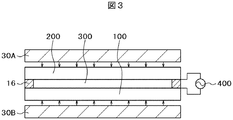
- FIG. 3 is a schematic cross-sectional view showing an acceleration test for evaluating the light resistance of the liquid crystal display panel.
- the TFT substrate 100 and the opposing substrate 200 are adhered to each other by the sealing material 16, and the liquid crystal layer 300 is sandwiched inside. Since the test for evaluating light resistance is an accelerated test, no polarizing plate is attached.
- This liquid crystal display panel is operated under normal operating conditions. A vertical electric field is applied to the liquid crystal layer 300 between the TFT substrate 100 and the facing substrate 200.
- FIG. 3 the liquid crystal display panel is irradiated from above and below with LED backlights 30A and 30B at a luminous intensity of 10000 cd / m 2. Then, the voltage retention rate is measured at predetermined time intervals.
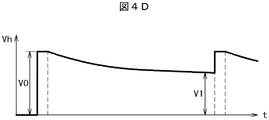
- 4A to 4D are diagrams showing the definition of the voltage holding ratio and the measuring method thereof.
- FIG. 4A is a schematic cross-sectional view for measuring the voltage holding ratio.
- FIG. 4B is an equivalent circuit of FIG. 4A.
- the liquid crystal display panel 10 is represented by a capacitor and a resistor.
- Vs is the power supply waveform for measurement
- Vh is the voltage at the liquid crystal terminal.
- FIG. 4C is a diagram showing power supply waveforms Vs for measurement.
- the measured voltage is a pulse having a peak value of V0 and a pulse width of 4 msec, and has a period of 1 sec.
- FIG. 4D is a waveform Vh of the voltage appearing at the terminal of the liquid crystal display panel corresponding to the measured voltage Vs. If there is no deterioration of the liquid crystal layer, the terminal voltage Vh does not decrease, but when the liquid crystal layer deteriorates and the electric resistance value decreases, the voltage decreases to, for example, V1 by the time the next measurement pulse is applied.
- V1 / V0 is referred to as a voltage retention rate. The closer V1 / V0 is to 1, the better.
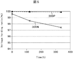
- FIG. 5 is a graph comparing the voltage retention rates of the negative type liquid crystal display 300N and the positive type liquid crystal display 300P under the conditions as shown in FIGS. 3 and 4A to 4D.
- the horizontal axis of FIG. 5 is time (h), and the vertical axis is the voltage holding ratio (%).
- the voltage holding ratio of the positive type liquid crystal 300P hardly decreases even after about 300 hours, but the voltage holding ratio of the negative type liquid crystal 300N decreases to about 97.3%.
- An object of the present invention is a configuration in which two liquid crystal display panels are stacked to increase the contrast of the liquid crystal display device, and even when a negative type liquid crystal display panel is used, deterioration of the characteristics of the negative type liquid crystal display panel can be suppressed. Is to realize.
- FIG. 6 is a plan view of the liquid crystal display panel.
- FIG. 6 is common to both the first liquid crystal display panel and the second liquid crystal display panel.
- the TFT substrate 100 and the opposing substrate 200 are adhered to each other by the sealing material 16, and a liquid crystal layer is sandwiched between the TFT substrate 100 and the opposing substrate 200.
- a display region 14 is formed in a portion where the TFT substrate 100 and the facing substrate 200 overlap.
- Scanning lines 11 extend in the horizontal direction (x direction) and are arranged in the vertical direction (y direction) in the display area 14 of the TFT substrate 100. Further, the video signal lines 12 extend in the vertical direction and are arranged in the horizontal direction. The area surrounded by the scanning line 11 and the video signal line 12 is the pixel 13.
- a pixel having such a configuration may be referred to as a sub-pixel, but in the present specification, it is referred to as a pixel.
- the TFT substrate 100 is formed larger than the opposing substrate 200, and the portion where the TFT substrate 100 does not overlap the opposing substrate 200 is the terminal region 15.
- a flexible wiring board 17 is connected to the terminal area 15.
- the driver IC that drives the liquid crystal display device is mounted on the flexible wiring board 17.
- FIG. 7 is a plan view of pixels in the display area of the liquid crystal display device corresponding to FIG. FIG. 7 is common to both the first liquid crystal display panel and the second liquid crystal display panel.
- FIG. 7 is a liquid crystal display device of a type called FFS (Fringe Field Switching) mode, which belongs to the IPS (In Plane Switching) mode.
- FFS Flexible Field Switching
- the scanning lines 11 extend in the horizontal direction (x direction) and are arranged in the vertical direction (y direction).
- the video signal lines 12 extend in the vertical direction and are arranged in the horizontal direction.
- a pixel electrode 143 is formed in a region surrounded by the scanning line 11 and the video signal line 12.
- An oxide semiconductor TFT is formed between the video signal line 12 and the pixel electrode 143.
- the light-shielding film is omitted.
- the drain electrode 110 is connected to the video signal line 12 via the through hole 130 and extends in the direction of the oxide semiconductor TFT formed in the upper adjacent pixel.
- One end of the oxide semiconductor film 109 is laminated and connected to the drain electrode 110 below the video signal line 12.
- the oxide semiconductor film 109 passes under the scanning line 11, and at this time, a TFT channel is formed.
- the scanning line 11 also serves as the gate electrode 114 in FIG.
- Boron (B) is doped in the oxide semiconductor film 109 except for the gate electrode 114, that is, the channel portion immediately below the scanning line 11, for example, by ion implantation to provide continuity.
- phosphorus (P) or argon (Ar) can be used as the ions by ion implantation.
- the ion-implanted portion of the oxide semiconductor film 109 is the n + region.
- the other end of the oxide semiconductor film 109 is laminated and connected to the source electrode 111.
- the source electrode 111 extends to the pixel electrode 143 side and is connected to the contact electrode 122 via the through hole 131.
- the contact electrode 122 is connected to the pixel electrode 143 via a through hole 135 formed in the organic passivation film 140 and a through hole 136 formed in the capacitive insulating film.
- the pixel electrode 143 is formed in a comb-teeth shape.
- a common electrode 141 is formed in a plane under the pixel electrode 143.
- electric lines of force are generated between the pixel electrode 143 and the common electrode 141 to rotate the liquid crystal molecules and control the transmittance of the liquid crystal in the pixel.
- Oxide semiconductors include IGZO (Indium Gallium Zinc Oxide), ITZO (Indium Tin Zinc Oxide), ZnON (Zinc Oxide Nitride), IGO (Indium Gallium Oxide), and the like.
- the TFT is not limited to the oxide semiconductor TFT, and a polysilicon TFT or the like may be used.
- FIG. 8 is a cross-sectional view of a general IPS type liquid crystal display device corresponding to the AA cross section of FIG. 9 to 11 show cross-sectional views of the first liquid crystal display panel and the second liquid crystal display panel used in the present invention in addition to FIG. The configuration and the operation thereof when various liquid crystal display panels of FIGS. 8 to 11 are combined will be described in Examples described later.
- the undercoat film 102 is formed so as to cover the TFT substrate 100.
- the base film 102 prevents impurities from a substrate made of a resin such as glass or polyimide from contaminating the oxide semiconductor film 109.
- the base film 102 is often formed of a laminated film of a silicon oxide film (SiO) and a silicon nitride film (SiN).
- a light-shielding film 106 is formed of metal on the base film 102. As this metal, the same metal as the gate electrode and the like described later may be used.
- the light-shielding film 106 is for blocking light from the backlight so that the channel portion of the TFT formed later is not irradiated with the light from the backlight. If necessary, the light-shielding film 106 can also be used as a shield electrode for preventing the influence on the TFT when the substrate 100 is charged. It can also be used as a lower gate electrode by applying a gate voltage.
- a buffer insulating film 108 is formed so as to cover the light-shielding film 106.
- the buffer insulating film 108 is formed of a silicon oxide film. This is to supply oxygen to the oxide semiconductor film 109 formed in the upper layer and to prevent the light-shielding film 106 formed of metal from depriving the oxide semiconductor 109 formed in the upper layer of oxygen.
- the buffer insulating film 108 acts as the lower gate insulating film.
- the oxide semiconductor film 109 constituting the TFT is formed on the buffer insulating film 108.
- the oxide semiconductor film 109 can be formed by sputtering.
- the thickness of the oxide semiconductor film 109 is 10 nm to 100 nm. In this embodiment, for example, an IGZO film having a thickness of 50 nm is used for the oxide semiconductor film 109.
- the semiconductor film 109 is composed of a channel region 1090, a drain region 1091, and a source region 1092.
- the drain region 1091 and the source region 1092 are imparted with conductivity by ion implantation using the gate electrode 114 as a mask.
- the channel region 1090 is located directly below the gate electrode 114.
- the drain electrode 110 is laminated on one end of the oxide semiconductor film 109, and the source electrode 111 is laminated on the other end.
- the drain electrode 110 and the source electrode 111 can be formed of the same metal as the gate electrode 114, or can be formed of a Ti film.
- the portion laminated with the drain electrode 110 and the source electrode 111 is conductive because oxygen is extracted by the metal.
- the gate insulating film 112 is formed of SiO so as to cover the oxide semiconductor film 109, the drain electrode 110, and the source electrode 111.
- the gate insulating film 112 is an oxygen-rich film, and supplies oxygen to the channel region 1090 of the oxide semiconductor film 109 to stabilize the characteristics of the oxide semiconductor TFT.
- the gate electrode 114 is formed on the gate insulating film 112.
- the gate electrode 114 is formed of, for example, a laminated film of Ti—Al—Ti (titanium-aluminum-titanium), a MoW alloy, or the like. As shown in FIG. 7, in this embodiment, the scanning line 11 is also used as the gate electrode 114.
- an aluminum oxide film may be formed between the gate electrode 114 and the gate insulating film 112. This is to supply more oxygen to the channel region 1090 of the oxide semiconductor film 109 to further stabilize the characteristics of the TFT.
- the aluminum oxide film in this case may be about 10 nm.
- An interlayer insulating film 115 is formed so as to cover the gate electrode 114.
- the interlayer insulating film 115 often has a two-layer structure of a silicon oxide film and a silicon nitride film. Which film is used as the upper layer or the lower layer depends on the purpose of use of the product and the like.
- a through hole 130 is formed in the interlayer insulating film 115 and the gate insulating film 112 to connect the video signal line 12 and the drain electrode 110, and a through hole 131 is formed to connect the contact electrode 122 and the source electrode 111. do.
- the contact electrode 122 extends over the interlayer insulating film 115 and connects to the pixel electrode 143 via through holes 135 and 136.
- the organic passivation film 140 is formed so as to cover the interlayer insulating film 115.
- the organic passivation film 140 is formed of, for example, an acrylic resin or the like.
- the organic passivation film 140 has a role as a flattening film, and is formed as thick as about 2 to 4 ⁇ m in order to reduce the stray capacitance between the video signal line 12 and the common electrode 141.
- Through holes 135 are formed in the organic passivation film 140 to connect the contact electrode 122 and the pixel electrode 143.
- a common electrode 141 is formed on the organic passivation film 140 by a transparent conductive film such as ITO (Indium Tin Oxide).
- the common electrode 141 is formed in a planar shape.
- a capacitive insulating film 142 is formed of a silicon nitride film so as to cover the common electrode 141.
- the pixel electrode 143 is formed by covering the capacitive insulating film 142 with a transparent conductive film such as ITO.
- the pixel electrode 143 is formed in a comb-teeth shape.
- the capacitive insulating film 142 is so called because it constitutes a pixel capacitance between the common electrode 141 and the pixel electrode 143.
- An alignment film 144 is formed so as to cover the pixel electrode 143.
- the alignment film 144 defines the initial orientation direction of the liquid crystal molecule 301.
- an orientation treatment by rubbing or a photoalignment treatment using polarized ultraviolet rays is used as the alignment treatment of the alignment film 144. Since the pretilt angle is not required in the IPS mode, the photo-alignment treatment is advantageous.
- the facing substrate 200 is arranged with the liquid crystal layer 300 interposed therebetween.
- a color filter 201 and a black matrix 202 are formed on the facing substrate 200, and an overcoat film 203 is formed on the color filter 201 and the black matrix 202.
- the alignment film 204 is formed on the overcoat film 203.
- the action and alignment treatment of the alignment film 204 are the same as those of the alignment film 144 on the TFT substrate 100 side.
- FIG. 9 is an example of a liquid crystal display panel used in the present invention.
- the liquid crystal display panel having the configuration of FIG. 9 is used in either the first liquid crystal display panel 10 or the second liquid crystal display panel 20 not for image formation but for improving the contrast ratio.
- the difference between FIG. 9 and FIG. 8 is that the color filter, the black matrix, and the overcoat film are not present in the facing substrate 200.
- the configuration of FIG. 9 can form an image, but cannot form a color image.
- the color image is formed by another liquid crystal display panel.
- the color filter since the color filter is not formed, the light transmittance can be increased and the decrease in screen brightness can be suppressed.
- FIG. 10 is another example of the liquid crystal display panel used in the present invention.
- the liquid crystal display panel having the configuration of FIG. 10 is used in either the first liquid crystal display panel 10 or the second liquid crystal display panel 20 not for image formation but for improving the contrast ratio.
- the difference between FIG. 10 and FIG. 8 is that the color filter does not exist in the facing substrate 200.
- the difference between FIG. 10 and FIG. 9 is that the black matrix 202 and the overcoat film 203 are present in FIG.
- the configuration of FIG. 9 When the configuration of FIG. 9 is used as the first liquid crystal display panel 10, a photocurrent may be generated in the TFT due to the influence of external light, or the image quality may be deteriorated due to reflection from the video signal line 12 or the scanning line 11. be.
- the configuration of FIG. 10 is advantageous when the liquid crystal display panel of the configuration of FIG. 10 is used as the first liquid crystal display panel because the influence of external light and the reflection of external light can be suppressed by the black matrix 202.
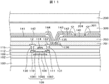
- FIG. 11 is still another example of the liquid crystal display panel used in the present invention.
- the color filter 201 is formed not on the facing substrate 200 side but on the TFT substrate 100 side.
- the color filter 201 is formed so as to cover the interlayer insulating film 115, the drain electrode 12, the source electrode 122, and the like, and the overcoat film 203 is formed on the color filter 201.
- the color filter is formed in either red, green, or blue for each pixel.
- the thickness of the color filter 201 is about 2 microns
- the thickness of the overcoat film 203 is about 2 microns.
- the overcoat film 203 also serves as a flattening film.
- the liquid crystal display panel having the configuration of FIG. 11 may be used for either the first liquid crystal display panel 10 or the second liquid crystal display panel 20.
- FIG. 12 is still another example of the liquid crystal display panel used in the present invention.
- the color filter 201 is formed not on the facing substrate 200 side but on the TFT substrate 100 side.
- the difference between FIG. 12 and FIG. 11 is that the black matrix 201 and the overcoat film 203 are formed on the facing substrate 200.
- the organic passivation film 140 is formed on the color filter 201 formed on the TFT substrate 100 side, but this may be the same as the overcoat film 203 of FIG.
- FIG. 12 is advantageous when the liquid crystal display panel of the configuration of FIG. 12 is used as the first liquid crystal display panel because the influence of external light and the reflection of external light can be suppressed by the black matrix 202.
- Other features of the configuration of FIG. 12 are the same as described with reference to FIG.
- either a negative type liquid crystal or a positive type liquid crystal can be used for the liquid crystal layer 300.
- the feature of the present invention is that when a negative liquid crystal display is used in the liquid crystal display panels of FIGS. 8 to 12, or a negative liquid crystal display 300N or a negative liquid crystal display 300N is used for either the first liquid crystal display panel 10 or the second liquid crystal display panel 20.
- the positive liquid crystal display 300P it is possible to realize a liquid crystal display device in which the contrast ratio is improved and the decrease in brightness and the decrease in light resistance are suppressed.
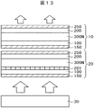
- FIG. 13 is a cross-sectional view showing the first embodiment of the first embodiment.
- the color filter 201 is formed on the TFT substrate 100 side. That is, the configuration of FIG. 11 is used.
- the configuration of FIG. 9 is used for the first liquid crystal display panel 10.
- the first liquid crystal display panel 10 in FIG. 13 does not form a color image, but is used as a panel for improving the contrast ratio. If a problem such as external light reflection occurs in the first liquid crystal display panel 10, the configuration shown in FIG. 10 may be used as the first liquid crystal display panel 10.
- FIG. 14 is a cross-sectional view showing a second embodiment of the first embodiment.
- the feature of FIG. 14 is that a negative liquid crystal display 300N is used for the first liquid crystal display panel 10 and a positive liquid crystal display 300P is used for the second liquid crystal display panel.
- a color filter is not formed on the second liquid crystal display panel 20 close to the backlight 30. That is, it has the configuration shown in FIG.
- a negative liquid crystal display is used for the first liquid crystal display panel 10, but the color filter is formed on the TFT substrate side. That is, it has the configuration shown in FIG.
- the backlight light that has passed through the second liquid crystal display panel 20 and the color filter 201 formed on the TFT substrate 100 of the first liquid crystal display panel is incident on the negative liquid crystal display 300N, it is more negative than the first form.
- the light intensity incident on the liquid crystal 300N is further reduced, and the problem of light resistance of the negative liquid crystal 300N is further reduced.
- the screen brightness can be improved by 15% as compared with the case where both liquid crystal display panels use positive liquid crystal. If a problem such as external light reflection occurs in the first liquid crystal display panel 10, the configuration shown in FIG. 12 may be used as the first liquid crystal display panel 10.
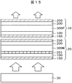
- FIG. 15 is a cross-sectional view showing a third embodiment of the first embodiment.
- the feature of FIG. 15 is that a negative liquid crystal display 300N is used for the second liquid crystal display panel 20 close to the backlight 30, and a positive liquid crystal display 300P is used for the first liquid crystal display panel 10.
- the second liquid crystal display panel 20 close to the backlight 30 is a negative liquid crystal display 300N, but since the color filter 201 is formed on the TFT substrate 100 side, there is a problem of light resistance as described in the first embodiment. Can be mitigated.
- the color filter 201 is not formed on the first liquid crystal display device 10 in which the positive liquid crystal 300P is used. That is, it has the configuration shown in FIG.
- the first liquid crystal display panel 10 is used for improving the contrast ratio. If a problem such as external light reflection occurs in the first liquid crystal display panel 10, the configuration shown in FIG. 10 may be used as the first liquid crystal display panel 10.
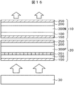
- FIG. 16 is a cross-sectional view showing a fourth embodiment of the first embodiment.
- the feature of FIG. 16 is that a positive liquid crystal display 300P is used for the second liquid crystal display panel 20 close to the backlight 30, and a negative liquid crystal display 300N is used for the first liquid crystal display panel 10.
- the second liquid crystal display panel 20 close to the backlight 30 is a positive liquid crystal display 300P, but the color filter 201 is formed on the TFT substrate 100 side.
- the color filter 201 is not formed on the first liquid crystal display device 10 in which the negative liquid crystal 300N is used. That is, it has the configuration shown in FIG. Since the backlight light incident on the negative liquid crystal display 300N passes through the color filter 201 formed on the TFT substrate 100 of the second liquid crystal display panel, the light intensity is reduced and the first liquid crystal display panel 10 The problem of light resistance of the negative type liquid crystal 300N in the above is alleviated. If a problem such as external light reflection occurs in the first liquid crystal display panel 10, the configuration shown in FIG. 10 may be used as the first liquid crystal display panel.
- a color filter 201 is formed on the TFT substrate 100 side.
- the backlight light passes through the color filter 201 and then enters the negative liquid crystal display 300N.
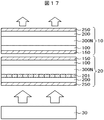
- FIG. 17 is a cross-sectional view showing the first embodiment of the second embodiment.
- both the first liquid crystal display panel 10 and the second liquid crystal display panel 20 use a negative liquid crystal display 300N.
- the second liquid crystal display panel 20 close to the backlight 30 is used upside down. That is, the configuration of the second liquid crystal display panel 20 is the same as that of FIG. 8, but FIG. 8 is arranged upside down. That is, since the opposing substrate 200 on which the color filter 201 is formed is close to the backlight 30, the backlight light incident on the negative liquid crystal layer 300N has already passed through the color filter 201 and its intensity has already decreased. , The problem of light resistance of the negative type liquid crystal 300N can be alleviated.
- the first liquid crystal display panel 10 in FIG. 17 uses a negative liquid crystal display 300N, but the configuration is the same as that of FIG. If there is a problem such as reflection of external light on the first liquid crystal display panel 10, the configuration shown in FIG. 10 may be used. Further, the reflection of external light due to wiring or the like due to the use of the second liquid crystal display panel 20 turned upside down can also be reduced by using the configuration of FIG.
- FIG. 18 is a cross-sectional view showing a second embodiment of the second embodiment.
- a negative liquid crystal display 300N is used for the first liquid crystal display panel 10
- a positive liquid crystal display 300P is used for the second liquid crystal display panel.
- the first liquid crystal display panel 10 using the negative liquid crystal display 300N is used upside down. That is, the configuration of the first liquid crystal display panel 10 is the same as that of FIG. 8, but FIG. 8 is arranged upside down.
- the second liquid crystal display panel 20 close to the backlight 30 may use the configuration shown in FIG.
- FIG. 19 is a cross-sectional view showing a third embodiment of the second embodiment.
- a positive liquid crystal display 300P is used for the first liquid crystal display panel 10
- a negative liquid crystal display 300N is used for the second liquid crystal display panel 20.
- the second liquid crystal display panel 20 using the negative liquid crystal display 300N is used upside down. That is, the configuration of the second liquid crystal display panel 20 is the same as that of FIG. 8, but FIG. 8 is arranged upside down.
- the configuration and operation of the first liquid crystal display panel 10 in FIG. 19 are the same as those described in the first embodiment shown in FIG.
- the difference between FIG. 19 and FIG. 17 is that the first liquid crystal display panel 10 uses a positive liquid crystal 300P.
- the configuration of the first liquid crystal display panel 10 can be the same as that of FIG. 9, but if the reflection of external light or the like becomes a problem, the configuration of FIG. 10 may be used.
- a white LED Light Emitting Diode
- the white LED there are cases where three LEDs that emit red, green, and blue, respectively, are used, and cases where a blue LED is used in combination with a YAG: Ce phosphor that emits yellow light.
- the emission spectrum of the backlight when using three LEDs is described as Three wave luminescences, and the emission spectrum of the backlight when using a combination of a blue LED and a YAG phosphor is described as YAG. It is a graph.
- the horizontal axis is the wavelength and the vertical axis is the standardized emission intensity.
- the emission spectrum of the backlight used in the liquid crystal display device is configured to exist in the visible light region.
- wavelengths of around 340 nm or 320 nm are also present, for example, in a slight amount in the normalized emission intensity corresponding to the vertical axis of FIG.
- ultraviolet rays having a large energy of about 340 nm or 320 nm affect the light resistance when absorbed by the liquid crystal layer.
- FIG. 21 is a graph showing absorption spectra for six types of liquid crystal materials.
- the horizontal axis is the wavelength and the vertical axis is the absorbance.
- the measuring device used was a spectroscopic altimeter U-3310 manufactured by Hitachi, Ltd.
- the absorption end moves to the short wavelength side in the order of the liquid crystal materials A to F. That is, as the absorption edge of the material moves to the left side in FIG. 21, the absorption of ultraviolet rays becomes smaller.
- the problem of light resistance is reduced.
- the voltage retention rate is lowered and black spots are generated in the light resistance test.
- the liquid crystal materials D, E, and F maintain the voltage retention rate in the light resistance test, and black spots do not occur.
- FIG. 22 is a schematic diagram for measuring the absorbance of the liquid crystal material.
- the liquid crystal material 305 for measurement is a liquid crystal material used for a liquid crystal display panel diluted 100-fold with cyclohexane, and is housed in a quartz container so as to have a thickness of 10 mm. .. Quartz has almost zero absorptivity in the wavelength range of measurement.
- light Iin having a measurement wavelength is incident on the liquid crystal layer 305 from the left side of the liquid crystal material 305, and light Iout emitted from the liquid crystal layer is measured.
- the absorbance of the liquid crystal layer is defined by -log10 (Iout / Iin).
- the liquid crystal materials A, B, C, D, E, and F shown in FIG. 21 were measured for those materials diluted 100-fold with cyclohexane.
- a detailed examination of the results shown in FIG. 21 reveals that the absorbances of the liquid crystal materials A, B, and C are 0.01 or more and the absorbances of the liquid crystal materials D, E, and F are 0.01 or less at a wavelength of 340 nm. Do you get it. That is, if the absorbance of the liquid crystal is 0.01 or less at a wavelength of 340 nm, the problem of light resistance can be solved. Further, by setting the absorbance of the liquid crystal to 0.005 or less, a liquid crystal display device having further excellent light resistance can be realized.
- the absorption ends of the liquid crystal materials E and F are largely moved to the short wavelength side as compared with other materials. Specifically, the absorbance at a wavelength of 320 nm is 0.01 or less.
- the absorbance at a wavelength of 320 nm is 0.01 or less.
Landscapes
- Physics & Mathematics (AREA)
- Nonlinear Science (AREA)
- General Physics & Mathematics (AREA)
- Mathematical Physics (AREA)
- Chemical & Material Sciences (AREA)
- Crystallography & Structural Chemistry (AREA)
- Optics & Photonics (AREA)
- Engineering & Computer Science (AREA)
- Microelectronics & Electronic Packaging (AREA)
- Theoretical Computer Science (AREA)
- Liquid Crystal (AREA)
Abstract
本発明の課題は、2枚の液晶表示パネルを重ね合わせ、画面輝度と耐光性性能を劣化させることなく、高いコントラスト比を有する液晶表示装置を実現することである。このための構成例はつぎにとおりである。第1液晶表示パネル10の背面に第2液晶表示パネル20が配置し、前記第2液晶表示パネル20の背面にバックライト30が配置した液晶表示装置であって、前記第1液晶表示パネル10と前記第2液晶表示パネル20の一方のパネルは、TFTとカラーフィルタが形成されたTFT基板100と対向基板200との間にネガ型液晶300Nが挟持され、前記TFT基板100は前記対向基板200よりも前記バックライト30に近く、前記第1液晶表示パネル10と前記第2液晶表示パネル20の他方のパネルにはカラーフィルタが形成されていないことを特徴とする液晶表示装置。
Description
本発明は、液晶表示パネルを複数重ねて用いることによって、高コントラストを実現する液晶表示装置に関する。
液晶表示装置では画素電極および薄膜トランジスタ(TFT)等を有する画素がマトリクス状に形成されたTFT基板と、TFT基板に対向して対向基板が配置され、TFT基板と対向基板の間に液晶が挟持されている。そして画素毎に、液晶分子によりバックライトからの光の透過率を制御することによって画像を形成している。液晶表示装置はフラットで軽量であることから、色々な分野で用途が広がっている。
黒表示は、バックライトからの光を遮断することによって行うが、液晶表示パネルでは、完全に遮断することは困難である。したがって、液晶表示パネルにおけるコントラスト比は、1000:1程度である。特許文献1には、液晶表示パネルを2枚重ねて用いることによって、コントラスト比を上げる技術が記載されている。
液晶表示装置は、視野角が問題である。IPS(In Plane Switching)モードの液晶表示装置を使用することによって、視野角の問題は軽減されるが、完全ではない。IPSモードの液晶表示装置においても、画面を見る角度によって、特定の色が強調される問題が存在する。特許文献2には、ポジ型液晶材料を用いた液晶表示パネルとネガ型液晶材料を用いた液晶表示パネルを重ねて使用することによって、このような着色の問題を解決する構成が記載されている。
コントラスト比が1000:1の液晶表示パネルを2枚重ねれば、理論的には、コントラスト比が1000000(1M):1の表示装置を実現することができる。しかし、液晶表示パネルを2枚重ねることによって、バックライトからの光の透過率が低下し、画面の明るさが問題となる。
液晶材料には、液晶分子の長軸が電気力線に沿って配向するポジ型液晶(誘電率異方性が正)と、液晶分子の長軸が電気力線と直角方向に配向するネガ型液晶(誘電率異方性が負)が存在する。ネガ型液晶を用いた液晶表示パネル(以後ネガ型液晶表示パネルと称する)の透過率は、ポジ型液晶を用いた液晶表示パネル(以後ポジ型液晶表示パネルと称する)の透過率よりも高い。
そこで、ネガ型液晶表示パネルを用いることによって、液晶表示パネルを2枚使用することによる光透過率の問題は軽減することができる。しかし、ネガ型液晶表示パネルはバックライトを長時間照射した場合に、液晶の電気抵抗が低下し、液晶表示パネルの電圧保持率が低下するという問題を有している。本明細書では、このような問題を耐光性の問題とも表現する。この問題は、具体的には、画面の黒シミとして現れる。
本発明の課題は、液晶表示パネルを複数重ねて使用した液晶表示装置において、画面の輝度の低下を抑え、かつ、耐光性を対策した、コントラスト比の高い液晶表示装置を実現することである。
本発明は上記問題を克服するものであり、具体的な手段は次のとおりである。
(1)第1液晶表示パネルの背面に第2液晶表示パネルが配置し、前記第2液晶表示パネルの背面にバックライトが配置した液晶表示装置であって、前記第1液晶表示パネルと前記第2液晶表示パネルの一方のパネルは、TFTとカラーフィルタが形成されたTFT基板と対向基板との間にネガ型液晶が挟持され、前記TFT基板は前記対向基板よりも前記バックライトに近く、前記第1液晶表示パネルと前記第2液晶表示パネルの他方のパネルには、カラーフィルタが形成されていないことを特徴とする液晶表示装置。
(2)第1液晶表示パネルの背面に第2液晶表示パネルが配置し、前記第2液晶表示パネルの背面にバックライトが配置した液晶表示装置であって、前記第1液晶表示パネルと前記第2液晶表示パネルの一方のパネルは、TFTが形成されたTFT基板とカラーフィルタが形成された対向基板との間にネガ型液晶が挟持され、前記対向基板は前記TFT基板よりも前記バックライトに近く、前記第1液晶表示パネルと前記第2液晶表示パネルの他方のパネルには、カラーフィルタが形成されていないことを特徴とする液晶表示装置。
(3)第1液晶表示パネルの背面に第2液晶表示パネルが配置し、前記第2液晶表示パネルの背面にバックライトが配置した液晶表示装置であって、前記第1液晶表示パネルと前記第2液晶表示パネルの一方のパネルは、TFT基板と対向基板との間にネガ型液晶が挟持され、前記ネガ型液晶をシクロヘキサンによって100倍に希釈した場合の層厚10mmにおける、波長340nmに対する吸光度は0.01以下であり、前記第1液晶表示パネルと前記第2液晶表示パネルのいずれか一方のパネルにはカラーフィルタが形成され、前記第1液晶表示パネルと前記第2液晶表示パネルのいずれか他方のパネルには、カラーフィルタが形成されていないことを特徴とする液晶表示装置。
(4)第1液晶表示パネルの背面に第2液晶表示パネルが配置し、前記第2液晶表示パネルの背面にバックライトが配置した液晶表示装置であって、前記第1液晶表示パネルと前記第2液晶表示パネルの一方のパネルは、TFT基板と対向基板との間にネガ型液晶が挟持され、前記ネガ型液晶をシクロヘキサンによって100倍に希釈した場合の層厚10mmにおける、波長320nmに対する吸光度は0.01以下であり、前記第1液晶表示パネルと前記第2液晶表示パネルのいずれか一方のパネルにはカラーフィルタが形成され、前記第1液晶表示パネルと前記第2液晶表示パネルのいずれか他方のパネルには、カラーフィルタが形成されていないことを特徴とする液晶表示装置。
図1は、本発明における液晶表示装置の分解斜視図である。図1において、第1液晶表示パネル10と第2液晶表示パネル20が重ねて使用される。第2液晶表示パネル20の背面にバックライト30が配置している。第1液晶表示パネル10と第2液晶表示パネル20は同じ液晶表示パネルを用いてもよいが、全体としての光の透過率を向上させるために、カラーフィルタはいずれか一方のパネルのみに形成してもよい。
液晶表示パネルを2枚用いることによって、コントラスト比は向上するが、液晶表示装置としての透過率が低下し、その結果、画面の輝度が低下する。液晶表示パネルには、ポジ型液晶を用いたポジ型液晶表示パネルと、ネガ型液晶を用いたネガ型液晶表示パネルが存在するが、光の透過率は、ネガ型液晶表示パネルのほうが高い。
図2は、ネガ型液晶とポジ型液晶の動作を示す模式図と、ネガ型液晶とポジ型液晶の光の透過率を示すグラフである。図2の動作は、IPSモードの液晶表示装置の場合である。図2の動作図において、有機パッシベーション膜140の上にコモン電極141が形成され、容量絶縁膜142を挟んで画素電極143が形成されている。画素電極143の上には液晶層が存在している。なお、図2では配向膜は省略されている。
図2において、画素電極143に電圧が印加されると、コモン電極141との間に矢印で示す電気力線が発生し、液晶分子を回転させる。図2において、301Pはポジ型液晶分子の場合であり、301Nはネガ型液晶分子の場合である。図2では、動作の比較のために、ポジ型液晶分子301Pとネガ型液晶分子301Nを上下に並べて配置している。
図2において、ポジ型液晶分子301Pは、ほぼ、電気力線に沿って配向しているが、ネガ型液晶分子301Nは、電気力線と垂直方向に回転をしている。図2の上側には、液晶層の透過率を液晶分子の動作と対応させて記載している。ポジ型液晶300Pの場合は、液晶分子301Pが立っている部分に対応して透過率の極小値が存在し、液晶分子301Pが寝ている部分に対応して透過率の極大値が存在している。
一方、ネガ型液晶300Nの場合は、液晶分子301Nが回転していない部分および十分に回転した部分に極小値が存在し、その中間に極大値が存在している。全体としてみると、ネガ型液晶300Nの場合のほうが、ポジ型液晶300Pの場合よりも15%程度、透過率が高い。したがって、液晶表示パネルを2枚重ねて用いることによる画面輝度の低下は、ネガ型液晶表示パネルを用いることによって、軽減することができる。
しかし、ネガ型液晶表示パネルはポジ型液晶表示パネルに比べて、耐光性が劣る。つまり、液晶表示パネルを長時間バックライトにさらした場合、液晶層の電気抵抗が低下することによって、液晶表示パネルにおける電圧保持率が低下するが、ネガ型液晶表示パネルの場合、ポジ型液晶表示パネルの場合よりも、電圧保持率の低下が大きいということが問題である。
図3は、液晶表示パネルの耐光性を評価するための加速試験を示す断面模式図である。図3において、TFT基板100と対向基板200がシール材16によって接着し、内部に液晶層300が挟持されている。なお、耐光性を評価するための試験は加速試験のため、偏光板は貼り付けていない。この液晶表示パネルを通常の動作条件によって動作させる。なお、液晶層300には、TFT基板100と対向基板200の間で縦電界が印加される。
図3において、液晶表示パネルを上下からLEDバックライト30Aおよび30Bによって、10000cd/m2の光度で照射する。そして所定時間ごとに電圧保持率を測定する。図4A乃至図4Dは電圧保持率の定義およびその測定方法を示す図である。図4Aは、電圧保持率を測定するための断面模式図である。図4Bは、図4Aの等価回路である。図4Bにおいて、液晶表示パネル10は、コンデンサと抵抗で示されている。Vsは測定のための電源波形であり、Vhは液晶端子における電圧である。
図4Cは、測定のための、電源波形Vsを示す図である。測定電圧は、波高値V0、パルス幅4msecのパルスで、周期1secである。図4Dは、測定電圧Vsに対応して、液晶表示パネルの端子に現れる電圧の波形Vhである。液晶層の劣化が無ければ、端子電圧Vhは低下しないが、液晶層が劣化して電気抵抗値が低下すると、次の測定パルスが印加されるまでに、例えば、電圧V1にまで低下する。V1/V0を電圧保持率と称する。V1/V0は1に近いほどよい。
図5は、図3および図4A乃至図4Dのような条件によって、ネガ型液晶300Nとポジ型液晶300Pについて、電圧保持率を比較したグラフである。図5の横軸は時間(h)であり、縦軸は電圧保持率(%)である。図5において、ポジ型液晶300Pは、300時間程度経過しても、電圧保持率はほとんど低下しないが、ネガ型液晶300Nは、97.3%程度にまで低下する。
図2および図5からわかるように、ネガ型液晶表示パネルを用いる場合、画面輝度の問題は軽減することができるが、電圧保持率の低下、すなわち、耐光性の問題が生ずる。液晶表示パネルを2枚重ねて用いる場合は、画面輝度の低下を補償するために、バックライトの光強度を液晶表示パネルが1枚の場合よりも上げるので、耐光性の問題はより強調されることになる。本発明の課題は、液晶表示パネルを2枚重ねて液晶表示装置のコントラストを上げる構成において、ネガ型液晶表示パネルを使用した場合においても、ネガ型液晶表示パネルの特性劣化を抑えることができる構成を実現することである。
図6は液晶表示パネルの平面図である。図6は第1液晶表示パネル、第2液晶表示パネルとも共通である。図6において、TFT基板100と対向基板200がシール材16によって接着し、TFT基板100と対向基板200の間に液晶層が挟持されている。TFT基板100と対向基板200が重なっている部分に表示領域14が形成されている。
TFT基板100の表示領域14には、走査線11が横方向(x方向)に延在し、縦方向(y方向)に配列している。また、映像信号線12が縦方向に延在して横方向に配列している。走査線11と映像信号線12に囲まれた領域が画素13になっている。なお、このような構成による画素はサブ画素を呼ばれることもあるが、本明細書では画素と呼ぶ。
TFT基板100は対向基板200よりも大きく形成され、TFT基板100が対向基板200と重なっていない部分は端子領域15となっている。端子領域15にはフレキシブル配線基板17が接続している。液晶表示装置を駆動するドライバICはフレキシブル配線基板17に搭載されている。
図7は、図6に対応する液晶表示装置の表示領域における画素の平面図である。図7は第1液晶表示パネル、第2液晶表示パネルとも共通である。図7は、IPS(In Plane Switching)モードに属する、FFS(Fringe Field Swtiching)モードと呼ばれる方式の液晶表示装置である。図7において、走査線11が横方向(x方向)に延在し、縦方向(y方向)に配列している。また、映像信号線12が縦方向に延在し、横方向に配列している。走査線11と映像信号線12に囲まれた領域に画素電極143が形成されている。映像信号線12と画素電極143との間に酸化物半導体TFTが形成されている。なお、図7では、遮光膜は省略されている。
図7において、ドレイン電極110がスルーホール130を介して映像信号線12と接続し、上隣りの画素に形成される酸化物半導体TFTの方向に延在する。酸化物半導体膜109は、一方の端は映像信号線12の下方において、ドレイン電極110と積層して接続する。
酸化物半導体膜109は走査線11の下を通過するが、この時、TFTのチャネルが形成される。図7においては、走査線11が図8におけるゲート電極114の役割を兼ねている。酸化物半導体膜109には、ゲート電極114、すなわち、走査線11直下のチャネル部を除いて、例えば、イオンインプランテーションによって、ボロン(B)がドープされ、導通が与えられている。なお、イオンインプランテーションによるイオンは、ボロンの他、リン(P)あるいはアルゴン(Ar)を使用することが出来る。酸化物半導体膜109のイオンインプランテーションされた部分はn+領域となっている。
酸化物半導体膜109の他端はソース電極111と積層して接続する。ソース電極111は画素電極143側に延在し、スルーホール131を介してコンタクト電極122と接続する。コンタクト電極122は有機パッシベーション膜140に形成されたスルーホール135及び容量絶縁膜に形成されたスルーホール136を介して画素電極143と接続する。画素電極143は櫛歯状に形成されている。
画素電極143の下には、コモン電極141が平面状に形成されている。画素電極143に電圧が印加されると、図2で説明したように、コモン電極141との間に電気力線が発生して液晶分子を回転させ、画素における液晶の透過率を制御する。
酸化物半導体には、IGZO(Indium Gallium Zinc Oxide)、ITZO(Indium Tin Zinc Oxide)、ZnON(Zinc Oxide Nitride)、IGO(Indium Gallium Oxide)等がある。なお、TFTは酸化物半導体TFTに限らず、ポリシリコンTFT等を用いてもよい。
図8は、図7のA-A断面に相当する、一般的なIPS方式の液晶表示装置の断面図である。図9乃至図11は、図8の他に、本発明において使用される第1液晶表示パネルおよび第2液晶表示パネルにおける断面図を示す。図8乃至図11の液晶表示パネルを種々組み合わせる場合の構成及びその作用は、後で記載する実施例において説明する。
まず、一般的な構成である、図8の構造を説明する。図8において、TFT基板100を覆って下地膜102が形成されている。下地膜102は、ガラスあるいはポリイミド等の樹脂で形成された基板からの不純物が酸化物半導体膜109を汚染することを防止するものである。下地膜102は、シリコン酸化膜(SiO)及びシリコン窒化膜(SiN)の積層膜で形成される場合が多い。
下地膜102の上に遮光膜106が金属によって形成されている。この金属は、後で説明するゲート電極等と同じ金属を使用してもよい。遮光膜106は、後で形成されるTFTのチャネル部にバックライトからの光が照射されないように遮光するためのものである。遮光膜106は必要に応じて、基板100が帯電した場合の、TFTへの影響を防止するための、シールド電極として使用することもできる。また、ゲート電圧を印加することによって、下ゲート電極として使用することも出来る。
遮光膜106を覆ってバッファ絶縁膜108が形成されている。バッファ絶縁膜108は、シリコン酸化膜で形成される。上層に形成される酸化物半導体膜109に酸素を供給するためと、金属で形成された遮光膜106が上層に形成される酸化物半導体109から酸素を奪うことを防止するためである。なお、遮光膜106を下ゲート電極として使用する場合は、バッファ絶縁膜108は下ゲート絶縁膜として作用する。
図8において、バッファ絶縁膜108の上にTFTを構成する酸化物半導体膜109が形成されている。酸化物半導体膜109はスパッタリングによって形成することが出来る。酸化物半導体膜109の厚さは10nm乃至100nmである。本実施例では、酸化物半導体膜109には例えば厚さ50nmのIGZO膜が使用される。
半導体膜109は、チャネル領域1090とドレイン領域1091、ソース領域1092から構成される。ドレイン領域1091とソース領域1092は、ゲート電極114をマスクにしたイオンインプランテーションによって導電性が付与されている。そして、ゲート電極114の直下がチャネル領域1090となっている。
酸化物半導体膜109の一方の端部にドレイン電極110が積層され、他方の端部にソース電極111が積層されている。ドレイン電極110、ソース電極111は、ゲート電極114と同じ金属で形成することが出来るし、Ti膜で形成することも出来る。酸化物半導体膜109において、ドレイン電極110及びソース電極111と積層している部分は、酸素が金属によって抜き取られるので、導電性となっている。
酸化物半導体膜109、ドレイン電極110、ソース電極111を覆ってゲート絶縁膜112がSiOによって形成されている。ゲート絶縁膜112は酸素リッチな膜となっており、酸化物半導体膜109のチャネル領域1090に酸素を供給して酸化物半導体TFTの特性を安定化させている。
ゲート絶縁膜112の上にゲート電極114が形成されている。ゲート電極114は例えば、Ti-Al-Ti(チタンーアルミニウムーチタン)の積層膜、あるいは、MoW合金等によって形成される。図7に示すように、本実施例では、ゲート電極114は走査線11が兼用している。
図8では、省略されているが、ゲート電極114とゲート絶縁膜112の間に、アルミニウム酸化膜が形成される場合がある。酸化物半導体膜109のチャネル領域1090に酸素をより多く供給して、TFTの特性をより安定化させるためである。この場合のアルミニウム酸化膜は10nm程度でよい。
ゲート電極114を覆って層間絶縁膜115が形成されている。層間絶縁膜115は、酸化シリコン膜と窒化シリコン膜の2層構造となっている場合が多い。いずれの膜を上層、あるいは、下層にするかは、製品の使用目的等による。
図8において、層間絶縁膜115及びゲート絶縁膜112に、スルーホール130を形成して映像信号線12とドレイン電極110を接続し、スルーホール131を形成してコンタクト電極122とソース電極111を接続する。コンタクト電極122は、層間絶縁膜115の上を延在し、スルーホール135、136を介して画素電極143と接続する。
図8において、層間絶縁膜115を覆って有機パッシベーション膜140が形成されている。有機パッシベーション膜140は、例えば、アクリル樹脂等で形成される。有機パッシベーション膜140は平坦化膜としての役割を持ち、また、映像信号線12とコモン電極141間の浮遊容量を小さくするために、2乃至4μm程度と、厚く形成される。コンタクト電極122と画素電極143を接続するために、有機パッシベーション膜140にスルーホール135が形成される。
有機パッシベーション膜140の上にITO(Indium Tin Oxide)等の透明導電膜によってコモン電極141が形成される。コモン電極141は平面状に形成される。コモン電極141を覆って容量絶縁膜142がシリコン窒化膜によって形成されている。容量絶縁膜142を覆ってITO等の透明導電膜によって画素電極143が形成されている。画素電極143は櫛歯状に形成される。容量絶縁膜142は、コモン電極141と画素電極143との間において、画素容量を構成するので、このように呼ばれる。
画素電極143を覆って配向膜144が形成されている。配向膜144は液晶分子301の初期配向方向を規定する。配向膜144の配向処理は、ラビングによる配向処理か偏光紫外線を用いた光配向処理が用いられる。IPSモードではプレティルト角は必要ないので、光配向処理が有利である。
図8において、液晶層300を挟んで、対向基板200が配置している。対向基板200にはカラーフィルタ201とブラックマトリクス202が形成され、その上にオーバーコート膜203が形成されている。オーバーコート膜203の上に配向膜204が形成されている。配向膜204の作用および配向処理は、TFT基板100側の配向膜144と同じである。
図8において、コモン電極141と画素電極143との間に電圧が印加されると、図8の矢印で示すような電気力線が発生し、液晶分子301を回転させて液晶層300によるバックライトからの光の透過率を制御する。画素毎に光の透過率を制御することによって画像を形成する。
図9は、本発明において使用される液晶表示パネルの例である。図9の構成を有する液晶表示パネルは、第1液晶表示パネル10か第2液晶表示パネル20のいずれかにおいて、画像形成ではなく、コントラスト比の向上のために使用されるものである。図9が図8と異なる点は、対向基板200において、カラーフィルタ、ブラックマトリクスおよびオーバーコート膜が存在していないことである。
したがって、図9の構成は、画像を形成することはできるが、カラー画像は形成できない。カラー画像は、他の液晶表示パネルによって形成される。図9の構成は、カラーフィルタが形成されていないので、光の透過率を上げることができ、画面輝度の低下を抑えることができる。
図10は、本発明において使用される液晶表示パネルの他の例である。図10の構成を有する液晶表示パネルは、第1液晶表示パネル10か第2液晶表示パネル20いずれかにおいて、画像形成ではなく、コントラスト比の向上のために使用されるものである。図10が図8と異なる点は、対向基板200において、カラーフィルタが存在していないことである。また、図10が図9と異なる点は、図10では、ブラックマトリクス202とオーバーコート膜203が存在していることである。
図9の構成を第1液晶表示パネル10として使用した場合、外光の影響によってTFTに光電流が発生したり、映像信号線12や走査線11からの反射で画質を低下したりすることがある。図10の構成は、ブラックマトリクス202によって、外光の影響や外光の反射を抑制できるので、図10の構成の液晶表示パネルを第1液晶表示パネルとして使用する場合に有利である。
図11は、本発明において使用される液晶表示パネルのさらに他の例である。図11の液晶表示パネルは、カラーフィルタ201が対向基板200側ではなく、TFT基板100側に形成されている。図11において、層間絶縁膜115、ドレイン電極12、ソース電極122等を覆ってカラーフィルタ201が形成され、その上にオーバーコート膜203が形成されている。カラーフィルタは画素毎に、赤、緑、青のいずれかが形成されている。カラーフィルタ201の厚さは2ミクロン程度であり、オーバーコート膜203の厚さは2ミクロン程度である。オーバーコート膜203は平坦化膜の役割も有している。
図11において、対向基板200側には配向膜のみ形成されている。図11の構成では、バックライト30からの光が、液晶層300に入射するときは、理論的にはカラーフィルタ201によって、強度が1/3に低下している。したがって、液晶層300として、ネガ型液晶材料300Nを使用する場合においても、耐光性を向上させることができる。すなわち、ネガ型液晶材料300Nを使用する場合であっても電圧保持率の低下を抑制することができる。図11の構成を有する液晶表示パネルは、第1液晶表示パネル10、第2液晶表示パネル20のいずれに使用してもよい。
図12は、本発明において使用される液晶表示パネルのさらに他の例である。図12の液晶表示パネルは、カラーフィルタ201が対向基板200側ではなく、TFT基板100側に形成されている。図12が図11と異なる点は、対向基板200にブラックマトリクス201とオーバーコート膜203が形成されていることである。図12では、TFT基板100側に形成されたカラーフィルタ201の上に有機パッシベーション膜140が形成されているが、これは、図11のオーバーコート膜203と同じでもよい。
図11の構成を第1液晶表示パネル10として使用した場合、外光の影響によってTFTに光電流が発生したり、映像信号線12や走査線11からの反射で画質を低下したりすることがある。図12の構成は、ブラックマトリクス202によって、外光の影響や外光の反射を抑制できるので、図12の構成の液晶表示パネルを第1液晶表示パネルとして使用する場合に有利である。図12の構成の他の特徴は、図11で説明したのと同じである。
図8乃至図12で説明した液晶表示パネルにおいて、液晶層300には、ネガ型液晶、ポジ型液晶のいずれも使用することができる。本発明の特徴は、図8乃至図12の液晶表示パネルにおいて、ネガ型液晶を用いた場合、あるいは、第1液晶表示パネル10と第2液晶表示パネル20のいずれかにネガ型液晶300N、又は、ポジ型液晶300Pを用いることによって、コントラスト比を向上させるとともに、輝度の低下と耐光性の低下を抑制した液晶表示装置を実現できることである。
図13は、実施例1の第1の形態を示す断面図である。図13の特徴は、第1液晶表示パネル10、第2液晶表示パネル20ともネガ型液晶を用いている点である。したがって、2個のパネルにポジ型液晶を用いた場合に比べて、画面輝度は1.15×1.15=1.323倍に向上させることができる。
図13においては、バックライト30に近い第2液晶表示パネル20において、カラーフィルタ201はTFT基板100側に形成されている。すなわち、図11の構成を用いている。一方第1液晶表示パネル10には、図9の構成を用いている。図13における第1液晶表示パネル10は、カラー画像は形成しないが、コントラスト比向上用のパネルとして使用される。なお、第1液晶表示パネル10における外光反射等の問題が生ずる場合は、第1液晶表示パネル10として図10の構成を用いればよい。
図14は、実施例1の第2の形態を示す断面図である。図14の特徴は、第1液晶表示パネル10にネガ型液晶300Nを用い、第2液晶表示パネルにポジ型液晶300Pを用いている点である。ただし、バックライト30に近い第2液晶表示パネル20には、カラーフィルタは形成されていない。つまり、図9の構成となっている。第1液晶表示パネル10には、ネガ型液晶が使用されているが、カラーフィルタはTFT基板側に形成されている。つまり、図11の構成となっている。
ネガ型液晶300Nには、第2液晶表示パネル20と、第1液晶表示パネルのTFT基板100に形成されたカラーフィルタ201を通過したバックライト光が入射するので、第1の形態よりもネガ型液晶300Nに入射する光強度はさらに低下しており、ネガ型液晶300Nの耐光性の問題はさらに軽減される。画面輝度は、液晶表示パネルが2枚ともポジ型液晶を用いる場合に比べて15%向上させることができる。なお、第1液晶表示パネル10における外光反射等の問題が生ずる場合は、第1液晶表示パネル10として図12の構成を用いればよい。
図15は、実施例1の第3の形態を示す断面図である。図15の特徴は、バックライト30に近い第2液晶表示パネル20にネガ型液晶300Nを用い、第1液晶表示パネル10にポジ型液晶300Pを用いている点である。バックライト30に近い第2液晶表示パネル20は、ネガ型液晶300Nであるが、カラーフィルタ201がTFT基板100側に形成されているので、第1の形態で説明したように、耐光性の問題は軽減することができる。
ポジ型液晶300Pが使用されている第1液晶表示装置10にはカラーフィルタ201は形成されていない。すなわち、図9の構成になっている。第1液晶表示パネル10はコントラスト比向上のために使用されている。なお、第1液晶表示パネル10における外光反射等の問題が生ずる場合は、第1液晶表示パネル10として図10の構成を用いればよい。
図16は、実施例1の第4の形態を示す断面図である。図16の特徴は、バックライト30に近い第2液晶表示パネル20にポジ型液晶300Pを用い、第1液晶表示パネル10にネガ型液晶300Nを用いている点である。バックライト30に近い第2液晶表示パネル20は、ポジ型液晶300Pであるが、カラーフィルタ201がTFT基板100側に形成されている。
ネガ型液晶300Nが使用されている第1液晶表示装置10にはカラーフィルタ201は形成されていない。すなわち、図9の構成になっている。ネガ型液晶300Nに入射するバックライト光は、第2液晶表示パネルのTFT基板100に形成されたカラーフィルタ201を通過しているので、光の強度は小さくなっており、第1液晶表示パネル10におけるネガ型液晶300Nの耐光性の問題は軽減される。なお、第1液晶表示パネル10における外光反射等の問題が生ずる場合は、第1液晶表示パネルとして図10の構成を用いればよい。
実施例1では、ネガ型液晶300Nを用いた液晶表示パネルにカラー画像を形成する場合は、TFT基板100側にカラーフィルタ201を形成することを特徴としている。しかし、TFT基板100側にカラーフィルタ201を形成することが困難な場合がある。実施例2は、対向基板200側にカラーフィルタ201を形成した場合においても、バックライト光がカラーフィルタ201を通過した後、ネガ型液晶300Nに入射する構成を与えるものである。
図17は、実施例2の第1の形態を示す断面図である。図17では、第1液晶表示パネル10、第2液晶表示パネル20のいずれもネガ型液晶300Nを使用している。しかし、バックライト30に近い第2液晶表示パネル20は上下裏返しで使用している。すなわち、第2液晶表示パネル20の構成は図8と同じであるが、図8を上下逆転した状態で配置している。つまり、カラーフィルタ201が形成された対向基板200がバックライト30に近いために、ネガ型液晶層300Nに入射するバックライト光は、カラーフィルタ201を通過して、すでに強度が小さくなっているので、ネガ型液晶300Nの耐光性の問題は軽減することができる。
図17における第1液晶表示パネル10はネガ型液晶300Nを使用しているが、構成は図9の構成と同じである。なお、第1液晶表示パネル10における外光反射等の問題がある場合は、図10の構成を使用すればよい。また、第2液晶表示パネル20を裏返して使用することによる、配線等による外光反射も、図10の構成を用いることによって、軽減することができる。
図18は、実施例2の第2の形態を示す断面図である。図18では、第1液晶表示パネル10にネガ型液晶300Nを使用し、第2液晶表示パネルにポジ型液晶300Pを使用している。しかし、ネガ型液晶300Nを使用している第1液晶表示パネル10は上下裏返して使用している。すなわち、第1液晶表示パネル10の構成は図8と同じであるが、図8を上下逆転した状態で配置している。
図18の構成では、ネガ型液晶300Nには、第2液晶表示パネル20と、第1液晶表示パネル10の対向基板200に形成されたカラーフィルタ201を通過したバックライト光が入射するので、光の強度は減衰しており、ネガ型液晶300Nの耐光性の問題は軽減される。なお、バックライト30に近い第2液晶表示パネル20は、図9の構成を用いればよい。
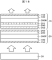
図19は、実施例2の第3の形態を示す断面図である。図19では、第1液晶表示パネル10にポジ型液晶300Pを使用し、第2液晶表示パネル20にネガ型液晶300Nを使用している。しかし、ネガ型液晶300Nを使用している第2液晶表示パネル20は上下裏返して使用している。すなわち、第2液晶表示パネル20の構成は図8と同じであるが、図8を上下逆転した状態で配置している。
図19における第1液晶表示パネル10の構成及び作用は図17に示す第1の形態で説明したのと同じである。図19が図17と異なる点は、第1液晶表示パネル10がポジ型液晶300Pを使用している点である。第1液晶表示パネル10の構成は、図9と同じ構成を使用することができるが、外光の反射等が問題になる場合は、図10の構成を使用すればよい。
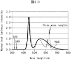
バックライトには白色LED(Light Emitting Diode)が使用される。白色LEDには、各々、赤、緑、青を発光する3個のLEDを使用する場合と、青色LEDに、黄色に発光するYAG:Ce蛍光体を組み合わせて使用する場合とがある。図20は、3個のLEDを使用する場合のバックライトの発光スペクトルをThree wave lengthsとし、青色LEDとYAG蛍光体の組み合わせを使用する場合の用いる場合のバックライトの発光スペクトルをYAGとして記載したグラフである。
図20において、横軸は波長、縦軸は、規格化された発光強度である。図20に示すように、液晶表示装置に使用されるバックライトの発光スペクトルは、可視光領域に存在するように構成されている。一方、340nm、あるいは、320nm付近の波長も、例えば、図20の縦軸に対応する規格化発光強度において、わずかながら存在する。しかし、このようなわずかな強度であっても、340nm、あるいは、320nm程度の、エネルギーの大きな紫外線は、液晶層に吸収されると、耐光性に影響を及ぼすことがわかってきた。
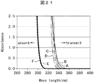
液晶層は、可視光領域は透過させ、紫外線領域は吸収する性質がある。したがって、わずかな量であっても、バックライトから紫外線が放射されると液晶層に吸収されて、液晶の耐光性の問題を生じさせる。図21は、6種類の液晶材料についての吸収スペクトルを示すグラフである。図21において、横軸は波長、縦軸は吸光度である。測定装置は日立製作所製分光高度計U-3310を用いた。図21において、液晶材料AからFの順で、吸収端が短波長側に移動する。すなわち、材料の吸収端が図21において、左側に移動するほど、紫外線の吸収は小さくなる。したがって、耐光性の問題が低減される。図21における液晶材料A、B、Cは、耐光性試験において、電圧保持率が低下し、黒シミが発生している。一方、液晶材料D、E、Fは、耐光性試験において、電圧保持率が維持され、黒シミは発生しない。
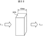
図22は、液晶材料の吸光度を測定する模式図である。図22において、測定用液晶材料305は、液晶表示パネルに使用される液晶材料を、シクロヘキサンによって100倍に希釈されたものであり、石英容器に、厚さが10mmになるように収容されている。石英は、測定の波長範囲では、吸収率はほとんどゼロである。図22において、液晶材料305の左側から測定波長の光Iinを液晶層305に入射し、液晶層から出射した光Ioutを測定する。液晶層の吸光度は、-log10(Iout/Iin)で定義される。
図21に示す液晶材料A、B、C、D、E、Fは、これらの材料をシクロヘキサンで100倍に希釈したものについて測定したものである。図21に示す結果を詳細に調べると、波長340nmにおいて、液晶材料A、B、Cの吸光度は0.01以上であり、液晶材料D、E、Fの吸光度は0.01以下であることが分かった。つまり、波長340nmにおいて、液晶の吸光度が0.01以下であれば、耐光性の問題をクリアすることができる。また、液晶の吸光度が0.005以下とすることによって、さらに耐光性に優れた液晶表示装置を実現することが出来る。
液晶材料E、Fは他の材料に比べて、吸収端が短波長側に大きく移動している。具体的には、波長320nmにおける吸光度は0.01以下である。液晶材料E、Fを使用することによって、ネガ型液晶の場合であっても、耐光性に優れた液晶表示装置を実現することが出来る。さらに、波長320nmにおける吸光度を0.005以下とすることによって、より耐光性に優れた液晶表示装置を実現することが出来る。
10…第1液晶表示パネル、 11…走査線、 12…映像信号線、 13…画素、 14…表示領域、 15…端子領域、 16…シール材、 17…フレキシブル配線基板、 20…第2液晶表示パネル、 30…バックライト、 100…TFT基板、 102…遮光膜、 106…遮光膜、 108…バッファ絶縁膜、 109…酸化物半導体膜、 110…ドレイン電極、 111…ソース電極、 112…ゲート絶縁膜、 114…ゲート電極、 115…層間絶縁膜、 122…コンタクト電極、 130…スルーホール、 131…スルーホール、 135…スルーホール、 136…スルーホール、 140…有機パッシベーション膜、 141…コモン電極、 142…容量絶縁膜、 143…画素電極、 144…配向膜、 150…下偏光板、 200…対向基板、 201…カラーフィルタ、 202…ブラックマトリクス、 203…オーバーコート膜、 204…配向膜、 250…上偏光板、 300…液晶層、 300N…ネガ型液晶、 300P…ポジ型液晶、 301…液晶分子、 301N…ネガ型液晶分子、 301P…ポジ型液晶分子、 305…試験用液晶層、 400…駆動電源、 1090…チャネル領域、 1091…ドレイン領域、 1092…ソース領域、 Vs…検査電圧、 Vh…保持電圧
Claims (18)
- 第1液晶表示パネルの背面に第2液晶表示パネルが配置し、前記第2液晶表示パネルの背面にバックライトが配置した液晶表示装置であって、
前記第1液晶表示パネルと前記第2液晶表示パネルの一方のパネルは、TFTとカラーフィルタが形成されたTFT基板と対向基板との間にネガ型液晶が挟持され、前記TFT基板は前記対向基板よりも前記バックライトに近く、
前記第1液晶表示パネルと前記第2液晶表示パネルの他方のパネルには、カラーフィルタが形成されていないことを特徴とする液晶表示装置。 - 前記他方のパネルには、ネガ型液晶が使用されていることを特徴とする請求項1に記載の液晶表示装置。
- 前記他方のパネルには、ポジ型液晶が使用されていることを特徴とする請求項1に記載の液晶表示装置。
- 前記一方のパネルは第1液晶表示パネルであることを特徴とする請求項1に記載の液晶表示装置。
- 前記一方のパネルは第2液晶表示パネルであることを特徴とする請求項1に記載の液晶表示装置。
- 前記他方のパネルには、ブラックマトリクスが形成されていることを特徴とする請求項1に記載の液晶表示装置。
- 第1液晶表示パネルの背面に第2液晶表示パネルが配置し、前記第2液晶表示パネルの背面にバックライトが配置した液晶表示装置であって、
前記第1液晶表示パネルと前記第2液晶表示パネルの一方のパネルは、TFTが形成されたTFT基板とカラーフィルタが形成された対向基板との間にネガ型液晶が挟持され、
前記対向基板は前記TFT基板よりも前記バックライトに近く、
前記第1液晶表示パネルと前記第2液晶表示パネルの他方のパネルには、カラーフィルタが形成されていないことを特徴とする液晶表示装置。 - 前記他方のパネルには、ネガ型液晶が使用されていることを特徴とする請求項7に記載の液晶表示装置。
- 前記他方のパネルには、ポジ型液晶が使用されていることを特徴とする請求項7に記載の液晶表示装置。
- 前記一方のパネルは第1液晶表示パネルであることを特徴とする請求項7に記載の液晶表示装置。
- 前記一方のパネルは第2液晶表示パネルであることを特徴とする請求項7に記載の液晶表示装置。
- 前記他方のパネルには、ブラックマトリクスが形成されていることを特徴とする請求項7に記載の液晶表示装置。
- 第1液晶表示パネルの背面に第2液晶表示パネルが配置し、前記第2液晶表示パネルの背面にバックライトが配置した液晶表示装置であって、
前記第1液晶表示パネルと前記第2液晶表示パネルの一方のパネルは、TFT基板と対向基板との間にネガ型液晶が挟持され、
前記ネガ型液晶をシクロヘキサンによって100倍に希釈した場合の層厚10mmにおける、波長340nmに対する吸光度は0.01以下であり、
前記第1液晶表示パネルと前記第2液晶表示パネルのいずれか一方のパネルにはカラーフィルタが形成され、
前記第1液晶表示パネルと前記第2液晶表示パネルのいずれか他方のパネルには、カラーフィルタが形成されていないことを特徴とする液晶表示装置。 - 前記ネガ型液晶をシクロヘキサンによって100倍に希釈した場合の層厚10mmにおける、波長340nmに対する吸光度は0.005以下であることを特徴とする請求項13に記載の液晶表示装置。
- 前記第1液晶表示パネルと前記第2液晶表示パネルの双方に前記ネガ型液晶が使用されていることを特徴とする請求項13に記載の液晶表示装置。
- 第1液晶表示パネルの背面に第2液晶表示パネルが配置し、前記第2液晶表示パネルの背面にバックライトが配置した液晶表示装置であって、
前記第1液晶表示パネルと前記第2液晶表示パネルの一方のパネルは、TFT基板と対向基板との間にネガ型液晶が挟持され、
前記ネガ型液晶をシクロヘキサンによって100倍に希釈した場合の層厚10mmにおける、波長320nmに対する吸光度は0.01以下であり、
前記第1液晶表示パネルと前記第2液晶表示パネルのいずれか一方のパネルにはカラーフィルタが形成され、
前記第1液晶表示パネルと前記第2液晶表示パネルのいずれか他方のパネルには、カラーフィルタが形成されていないことを特徴とする液晶表示装置。 - 前記ネガ型液晶をシクロヘキサンによって100倍に希釈した場合の層厚10mmにおける、波長320nmに対する吸光度は0.005以下であることを特徴とする請求項16に記載の液晶表示装置。
- 前記第1液晶表示パネルと前記第2液晶表示パネルの双方に前記ネガ型液晶が使用されていることを特徴とする請求項16に記載の液晶表示装置。
Priority Applications (2)
| Application Number | Priority Date | Filing Date | Title |
|---|---|---|---|
| JP2022508104A JPWO2021186901A1 (ja) | 2020-03-18 | 2021-01-26 | |
| US17/942,587 US20230280625A1 (en) | 2020-03-18 | 2022-09-12 | Liquid crystal display device |
Applications Claiming Priority (2)
| Application Number | Priority Date | Filing Date | Title |
|---|---|---|---|
| JP2020-047489 | 2020-03-18 | ||
| JP2020047489 | 2020-03-18 |
Related Child Applications (1)
| Application Number | Title | Priority Date | Filing Date |
|---|---|---|---|
| US17/942,587 Continuation US20230280625A1 (en) | 2020-03-18 | 2022-09-12 | Liquid crystal display device |
Publications (1)
| Publication Number | Publication Date |
|---|---|
| WO2021186901A1 true WO2021186901A1 (ja) | 2021-09-23 |
Family
ID=77771131
Family Applications (1)
| Application Number | Title | Priority Date | Filing Date |
|---|---|---|---|
| PCT/JP2021/002593 Ceased WO2021186901A1 (ja) | 2020-03-18 | 2021-01-26 | 液晶表示装置 |
Country Status (3)
| Country | Link |
|---|---|
| US (1) | US20230280625A1 (ja) |
| JP (1) | JPWO2021186901A1 (ja) |
| WO (1) | WO2021186901A1 (ja) |
Citations (4)
| Publication number | Priority date | Publication date | Assignee | Title |
|---|---|---|---|---|
| WO2013002084A1 (ja) * | 2011-06-27 | 2013-01-03 | シャープ株式会社 | 液晶表示装置及び液晶表示装置の製造方法 |
| JP2018072675A (ja) * | 2016-11-01 | 2018-05-10 | パナソニック液晶ディスプレイ株式会社 | 液晶表示装置 |
| JP2018072754A (ja) * | 2016-11-04 | 2018-05-10 | パナソニック液晶ディスプレイ株式会社 | 液晶表示装置 |
| JP2018097155A (ja) * | 2016-12-13 | 2018-06-21 | パナソニック液晶ディスプレイ株式会社 | 液晶表示装置 |
-
2021
- 2021-01-26 JP JP2022508104A patent/JPWO2021186901A1/ja active Pending
- 2021-01-26 WO PCT/JP2021/002593 patent/WO2021186901A1/ja not_active Ceased
-
2022
- 2022-09-12 US US17/942,587 patent/US20230280625A1/en not_active Abandoned
Patent Citations (4)
| Publication number | Priority date | Publication date | Assignee | Title |
|---|---|---|---|---|
| WO2013002084A1 (ja) * | 2011-06-27 | 2013-01-03 | シャープ株式会社 | 液晶表示装置及び液晶表示装置の製造方法 |
| JP2018072675A (ja) * | 2016-11-01 | 2018-05-10 | パナソニック液晶ディスプレイ株式会社 | 液晶表示装置 |
| JP2018072754A (ja) * | 2016-11-04 | 2018-05-10 | パナソニック液晶ディスプレイ株式会社 | 液晶表示装置 |
| JP2018097155A (ja) * | 2016-12-13 | 2018-06-21 | パナソニック液晶ディスプレイ株式会社 | 液晶表示装置 |
Also Published As
| Publication number | Publication date |
|---|---|
| JPWO2021186901A1 (ja) | 2021-09-23 |
| US20230280625A1 (en) | 2023-09-07 |
Similar Documents
| Publication | Publication Date | Title |
|---|---|---|
| JP5165169B2 (ja) | 液晶表示装置 | |
| JP3289099B2 (ja) | アクティブマトリクス型液晶表示装置およびその製造方法 | |
| US7982841B2 (en) | Method for manufacturing liquid crystal display device | |
| CN101387806B (zh) | 液晶显示面板及其制造方法 | |
| JP5460123B2 (ja) | 液晶表示装置 | |
| US8339557B2 (en) | Liquid crystal display panel | |
| US20180052347A1 (en) | Va type coa liquid crystal display panel | |
| KR102492032B1 (ko) | 표시 장치 및 이의 제조 방법 | |
| US20150346564A1 (en) | Liquid crystal display | |
| JP2015069195A (ja) | 液晶表示装置 | |
| CN103492938B (zh) | 液晶显示面板和具备该液晶显示面板的液晶显示装置 | |
| JP6220628B2 (ja) | 表示装置 | |
| US9335590B2 (en) | Liquid crystal display element and liquid crystal display device | |
| CN110412797A (zh) | 显示装置 | |
| CN106997117B (zh) | 液晶显示装置 | |
| WO2023168956A1 (zh) | 阵列基板、液晶显示面板和显示装置 | |
| US9817291B2 (en) | Liquid crystal display device | |
| US11709399B2 (en) | Liquid crystal display device | |
| US20160170263A1 (en) | Liquid crystal display device | |
| JP2014115561A (ja) | 液晶表示装置 | |
| US11703729B2 (en) | Display device | |
| US20230280625A1 (en) | Liquid crystal display device | |
| US12147127B2 (en) | Liquid crystal display | |
| US6525796B2 (en) | Liquid-crystal display device | |
| TWI858778B (zh) | 液晶顯示裝置 |
Legal Events
| Date | Code | Title | Description |
|---|---|---|---|
| 121 | Ep: the epo has been informed by wipo that ep was designated in this application |
Ref document number: 21770984 Country of ref document: EP Kind code of ref document: A1 |
|
| ENP | Entry into the national phase |
Ref document number: 2022508104 Country of ref document: JP Kind code of ref document: A |
|
| NENP | Non-entry into the national phase |
Ref country code: DE |
|
| 122 | Ep: pct application non-entry in european phase |
Ref document number: 21770984 Country of ref document: EP Kind code of ref document: A1 |