WO2021181752A1 - 生体用電極 - Google Patents
生体用電極 Download PDFInfo
- Publication number
- WO2021181752A1 WO2021181752A1 PCT/JP2020/041836 JP2020041836W WO2021181752A1 WO 2021181752 A1 WO2021181752 A1 WO 2021181752A1 JP 2020041836 W JP2020041836 W JP 2020041836W WO 2021181752 A1 WO2021181752 A1 WO 2021181752A1
- Authority
- WO
- WIPO (PCT)
- Prior art keywords
- electrode layer
- silver
- silica
- biological
- resin
- Prior art date
- Legal status (The legal status is an assumption and is not a legal conclusion. Google has not performed a legal analysis and makes no representation as to the accuracy of the status listed.)
- Ceased
Links
Images
Classifications
-
- A—HUMAN NECESSITIES
- A61—MEDICAL OR VETERINARY SCIENCE; HYGIENE
- A61B—DIAGNOSIS; SURGERY; IDENTIFICATION
- A61B5/00—Measuring for diagnostic purposes; Identification of persons
- A61B5/24—Detecting, measuring or recording bioelectric or biomagnetic signals of the body or parts thereof
- A61B5/25—Bioelectric electrodes therefor
-
- A—HUMAN NECESSITIES
- A61—MEDICAL OR VETERINARY SCIENCE; HYGIENE
- A61B—DIAGNOSIS; SURGERY; IDENTIFICATION
- A61B5/00—Measuring for diagnostic purposes; Identification of persons
- A61B5/24—Detecting, measuring or recording bioelectric or biomagnetic signals of the body or parts thereof
- A61B5/25—Bioelectric electrodes therefor
- A61B5/263—Bioelectric electrodes therefor characterised by the electrode materials
-
- A—HUMAN NECESSITIES
- A61—MEDICAL OR VETERINARY SCIENCE; HYGIENE
- A61B—DIAGNOSIS; SURGERY; IDENTIFICATION
- A61B2562/00—Details of sensors; Constructional details of sensor housings or probes; Accessories for sensors
- A61B2562/02—Details of sensors specially adapted for in-vivo measurements
- A61B2562/0209—Special features of electrodes classified in A61B5/24, A61B5/25, A61B5/283, A61B5/291, A61B5/296, A61B5/053
-
- A—HUMAN NECESSITIES
- A61—MEDICAL OR VETERINARY SCIENCE; HYGIENE
- A61B—DIAGNOSIS; SURGERY; IDENTIFICATION
- A61B2562/00—Details of sensors; Constructional details of sensor housings or probes; Accessories for sensors
- A61B2562/12—Manufacturing methods specially adapted for producing sensors for in-vivo measurements
- A61B2562/125—Manufacturing methods specially adapted for producing sensors for in-vivo measurements characterised by the manufacture of electrodes
-
- A—HUMAN NECESSITIES
- A61—MEDICAL OR VETERINARY SCIENCE; HYGIENE
- A61B—DIAGNOSIS; SURGERY; IDENTIFICATION
- A61B5/00—Measuring for diagnostic purposes; Identification of persons
- A61B5/24—Detecting, measuring or recording bioelectric or biomagnetic signals of the body or parts thereof
- A61B5/25—Bioelectric electrodes therefor
- A61B5/279—Bioelectric electrodes therefor specially adapted for particular uses
- A61B5/28—Bioelectric electrodes therefor specially adapted for particular uses for electrocardiography [ECG]
-
- A—HUMAN NECESSITIES
- A61—MEDICAL OR VETERINARY SCIENCE; HYGIENE
- A61B—DIAGNOSIS; SURGERY; IDENTIFICATION
- A61B5/00—Measuring for diagnostic purposes; Identification of persons
- A61B5/24—Detecting, measuring or recording bioelectric or biomagnetic signals of the body or parts thereof
- A61B5/30—Input circuits therefor
- A61B5/307—Input circuits therefor specially adapted for particular uses
- A61B5/308—Input circuits therefor specially adapted for particular uses for electrocardiography [ECG]
Definitions
- the present invention relates to a biological electrode.
- a biological electrode one provided with a polarizable electrode layer and a non-polarizing electrode layer containing silver and silver chloride has been used.
- Such biological electrodes are attached to patients for use in electrocardiography and the like. At this time, an X-ray image may be taken with the biological electrode attached to the patient. Therefore, it is preferable that the amount of silver in the biological electrode is reduced so that the electrode is not reflected in the X-ray image, and the X-ray transparency is improved. Further, it is preferable that the amount of silver is reduced in order to manufacture the biological electrode at low cost.
- Patent Document 1 describes a non-polarizing electrode layer in which a thin film of silver / silver chloride is formed on the polarizing electrode layer by a method such as printing or vapor deposition to a thickness of several ⁇ m. Is known to be equipped with.
- a biological electrode having a non-polarizing electrode layer formed by a resin composition in which silver / silver chloride is dispersed in a resin is known.
- Patent Document 2 describes a non-polarizing electrode layer (highly porous top conductive layer) formed by a conductive coating material containing a resin, silver / silver chloride particles, and carbon particles. Those with are described. According to this, it is said that the non-polarizing electrode layer becomes highly porous, so that the silver / silver chloride particles having a low content can exhibit the required electrical characteristics.
- the biological electrode of the prior art has a problem that the reduction of the silver content is insufficient, and in particular, the X-ray transparency is insufficient.
- the electrical performance of the biological electrode is lowered.
- a biological electrode manufactured by a method using carbon particles has a problem that non-polarity is lowered and electrical performance is insufficient.
- the American standard (ANSI / AAMI EC12: 2000) / (R) 2010) may not be fully satisfied.
- the biological electrode according to the present invention is The polar electrode layer and the non-polar electrode layer laminated on the polar electrode layer are provided.
- the non-polarizing electrode layer contains a resin, silver, and silver chloride supported on silica.
- the silver content is 150 to 300 parts by mass with respect to 100 parts by mass of the resin.
- the ratio of the content of the silver to the silver chloride is 97: 3 to 95: 5.
- the thickness of the non-polarizing electrode layer is 3 to 5 ⁇ m.
- the biological electrode according to the present invention is preferably used.
- the content of the silica is 20 to 50 parts by mass with respect to 100 parts by mass of the resin.
- the biological electrode according to the present invention is preferably used.
- the thickness of the polar electrode layer is 5 to 10 ⁇ m.
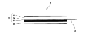
- FIG. 1 is a schematic view showing a cross-sectional structure of a biological electrode according to an embodiment.
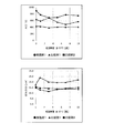
- FIG. 2 is a graph of the results shown in Table 1 of the examples.
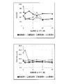
- FIG. 3 is a graph of the results shown in Table 3 of the examples.
- the biological electrode 1 of the present embodiment is used to acquire biological information such as an electrocardiogram, an electroencephalogram, and an electromyogram. Therefore, it is preferable that the biological electrode 1 sufficiently satisfies the American standard (ANSI / AAMI EC12: 2000 / (R) 2010).
- the impedance of the biological electrode 1 (hereinafter, also referred to as ACZ) is preferably 2,000 ⁇ or less, more preferably 1,000 ⁇ or less, and further preferably 750 ⁇ or less.
- the polarization of the biological electrode 1 after defibrillation load (which becomes an index of non-polarity and is also referred to as SDR / DCO below) is preferably 100 mV or less, and more preferably 20 mV or less.
- the biological electrode 1 preferably has storage stability, and for example, it is preferable that the above-mentioned electrical performance can be maintained for 5 weeks or more or 10 weeks or more under the condition of a temperature of 57 ° C.
- the biological electrode 1 is configured to be suitably used when an X-ray image is taken in parallel with the acquisition of the biological information.
- the biological electrode 1 of the present embodiment is laminated on a sheet-shaped base material 10 and one surface of the base material 10, and is an electrode layer 20 for detecting an electric signal from the living body. And have.
- the biological electrode 1 is used by connecting the lead wire 30 to the electrode layer 20.
- the base material 10 is usually formed of an electrically insulating film made of polyethylene terephthalate (PET).
- PET polyethylene terephthalate
- the electrically insulating film means a film having a volume resistivity of 1 ⁇ 10 13 ⁇ ⁇ cm or more.
- the thickness of the base material 10 is usually set to 5 to 100 ⁇ m.
- the lead wire 30 may be composed of, for example, a metal conductor and a covering material covering the metal conductor. Further, the conductor of the lead wire 30 is preferably a conductor formed by bundling conductive carbon fibers instead of the metal conductor so that the lead wire 30 is less likely to appear in the X-ray image. In the lead wire 30, the conductor at one end is electrically connected to the electrode layer 20.
- the electrode layer 20 is one of a polar electrode layer 22 formed on one surface of the base material 10, a non-polar electrode layer 24 formed on one surface of the polar electrode layer 22, and a non-polar electrode layer 24. It has a conductive gel layer 26 formed on the surface.
- the lead wire 30 is arranged between the non-polarizing electrode layer 24 and the conductive gel layer 26.
- the polarizable electrode layer 22 is formed of a carbon paste in which graphite and / or carbon powder is dispersed in a resin.
- the thickness of the polarizable electrode layer 22 is usually 2 to 100 ⁇ m. From the viewpoint that the ACZ of the biological electrode 1 is sufficiently reduced, the thickness of the polarizable electrode layer 22 is preferably 5 ⁇ m or more. Further, from the viewpoint that the biological electrode 1 can be manufactured at low cost, the thickness of the polar electrode layer 22 is preferably 10 ⁇ m or less.
- the non-polarizing electrode layer 24 contains a resin, silver, and silver chloride supported on silica. That is, in the non-polarizing electrode layer 24, a resin composition in which silver and silica supporting silver chloride are dispersed in a resin is printed, transferred, or coated on one surface of the polarizing electrode layer 22. It is formed by being covered with silica.
- silver chloride supported on silica may be referred to as silver chloride-supported silica.
- the thickness of the non-polarizing electrode layer 24 is preferably larger than 2 ⁇ m and smaller than 8 ⁇ m, and more preferably 3 to 5 ⁇ m. As a result, the biological electrode 1 has excellent X-ray transparency while maintaining the electrical performance of the biological electrode 1.
- the thickness of the polarizable electrode layer 22 and the non-polarizing electrode layer 24 is calculated as an average thickness by observing a cross section with a scanning electron microscope (SEM).
- SEM scanning electron microscope
- the conductive gel layer 26 is peeled off from the biological electrode 1, a section is cut out from the electrode layer 20 by a microtome or the like, and a cross section of the section is observed at a magnification of 10,000 times or less by SEM.
- a method of measuring the thickness of an arbitrary plurality of locations (for example, 9 locations) of the polarized electrode layer 22 and the non-polarizing electrode layer 24 and using the arithmetic average value of the measured thickness as the average thickness can be mentioned.
- thermoplastic resins such as polystyrene resin, polyester resin, polyurethane resin, acrylic resin, alkyd resin, phenoxy resin, butyral resin, and polyvinyl alcohol resin.
- silver powder can be used as the silver.
- the shape of the silver powder is not particularly limited, but is preferably spherical or scaly. Further, the silver powder is preferably surface-treated with a fatty acid such as stearic acid, thereby improving the dispersibility in the resin.
- the silver particle size is usually 4 ⁇ m or less, preferably 3 ⁇ m or less, and more preferably 2 ⁇ m or less so that the thickness of the non-polarizing electrode layer 24 can be set thin.
- the silver particle size means the median size (D50) measured by the laser diffraction / scattering type particle size distribution measuring device.
- the silver content is preferably larger than 140 parts by mass, more preferably 150 parts by mass or more, and further preferably 180 parts by mass or more with respect to 100 parts by mass of the resin. As a result, the ACZ of the biological electrode 1 is sufficiently reduced.
- the silver content is preferably 300 parts by mass or less, more preferably 250 parts by mass or less, and further preferably 200 parts by mass or less. As a result, the X-ray transparency of the biological electrode 1 becomes excellent.
- silver chloride-supported silica for example, one prepared by the method described in International Publication No. 2018/003702 is used. By supporting the silver chloride on the silica, aggregation of the silver chloride is avoided, and the silver chloride can be uniformly present in the non-polarizing electrode layer 24.
- the particle size of the silver chloride-supported silica is preferably 4 ⁇ m or less, more preferably 3 ⁇ m or less so that the thickness of the non-polarizing electrode layer 24 can be set thin.
- the particle size of the silver chloride-supported silica means the median diameter (D50) measured by a laser diffraction / scattering type particle size distribution measuring device.
- silica conventionally known ones can be used, and wet silica such as precipitation silica or gelation silica may be used, or dry silica may be used. Among them, gelation silica may be used. Is preferable.
- the specific surface area of the silica is preferably 20 m 2 / g or more and 1000 m 2 / g or less, and more preferably 400 m 2 / g or more and 700 m 2 / g or less.
- the specific surface area means a value measured by the BET method by adsorbing an inert gas.
- the pore volume of the silica is preferably 0.2 mL / g or more and 2.0 mL / g or less, and more preferably 0.3 mL / g or more and 0.6 mL / g or less.
- the pore volume means a value measured by a mercury porosimeter.
- the oil absorption of the silica is preferably 50 mL / 100 g or more and 500 mL / 100 g or less, and more preferably 70 mL / 100 g or more and 170 mL / 100 g or less.
- the oil absorption amount shall mean a value measured by the test method described in JIS K 5101-13-1.
- the average pore diameter of the silica is preferably 2 nm or more and 100 nm or less, and more preferably 2 nm or more and 7 nm or less.
- the average pore system means a value measured by a mercury porosimeter.
- the particle size of the silica is usually 4 ⁇ m or less, preferably 3 ⁇ m or less so that the thickness of the non-polarizing electrode layer 24 can be set thin.
- the particle size of the silica means the median diameter (D50) measured by the laser diffraction / scattering type particle size distribution measuring device.
- the content of the silica is usually 20 to 50 parts by mass and preferably 24 to 40 parts by mass with respect to 100 parts by mass of the resin.
- a dispersion in which the resin, the silver, and the silver chloride-supported silica are dispersed in an organic solvent is prepared.
- the dispersion has a viscosity such that the precipitation of the contained silver is suppressed.
- the content of the silica is preferably 20 parts by mass or more, and more preferably 24 parts by mass or more with respect to 100 parts by mass of the resin.
- the amount of silver chloride used is as small as possible. As a result, contamination of the equipment for preparing the resin composition and the equipment for coating and the like is reduced. In addition, since the use of halogen substances in the production of the biological electrode 1 is reduced, it is also preferable in terms of the environment. From the viewpoint of maintaining the electrical performance of the biological electrode 1 while reducing the amount of silver chloride used, the ratio of the silver content to the silver chloride content is 97: 3 to 95. : 5 is preferable.
- the silver chloride content is usually 5 to 45%, preferably 10 to 30%, based on the total amount of silver chloride-supported silica. More preferably, it is ⁇ 25%.
- the conductive gel layer 26 is a layer that brings the biological electrode 1 into contact with the surface of the skin.
- the conductive gel layer 26 contains an alkali halide such as sodium chloride as an electrolyte.
- an alkali halide such as sodium chloride as an electrolyte.
- the method for producing the biological electrode 1 includes a first layer forming step S1 in which the polarizable electrode layer 22 is formed on one surface of the base material 10, and a non-polarizing electrode layer 24 is formed on one surface of the polarizable electrode layer 22.
- the second layer forming step S2 is provided.
- a carbon paste prepared by dispersing resin, graphite and / or carbon powder in an organic solvent is coated on one surface of the base material 10, and then the organic solvent is removed by drying to obtain a minute amount. This is a step of forming the polar electrode layer 22.
- the second layer forming step S2 includes a step of preparing a dispersion in which silver and silver chloride-supported silica are dispersed in a resin, and a non-polarizing electrode layer 24 in which the dispersion is coated on the surface of the polarizing electrode layer 22. Has a step of forming.
- the resin is dissolved in an organic solvent, the silver and the silver chloride-supported silica are dispersed, and the dispersion is prepared by stirring at room temperature.
- organic solvent examples include ketone solvents such as methyl ethyl ketone (MEK) and cyclohexanone, ester solvents such as ethyl acetate, cyclic alkane solvents such as cyclohexane and methylcyclohexane, benzene and xylene (isomers of o-xylene and m-).
- An aromatic solvent having one benzene ring such as xylene (including xylene and p-xylene) and toluene is preferable.
- a linear or branched alkane solvent having 5 to 8 carbon atoms is also preferably used.
- Examples of such a solvent include n-pentane having 5 carbon atoms, 2-methylbutane, 2,2-dimethylpropane, n-hexane having 6 carbon atoms, 3-methylpentane, 2-methylpentane, and 2,3-.
- the content of the organic solvent with respect to the total amount of the dispersion is preferably 60 to 70% by mass.
- the dispersion is coated on the surface of the polarizing electrode layer 22.
- the coating method include printing, transfer, and coating. Since the viscosity of the dispersion of the present embodiment is increased by containing silica, the precipitation of silver is suppressed at the time of printing or the like. This makes it possible to uniformly disperse the silver in the non-polarizing electrode layer 24.
- the organic solvent is dried and removed to form a non-polarizing electrode layer 24.
- the dispersion has an increased viscosity, the precipitation of silver is suppressed even during this drying.
- the biological electrode 1 is The polar electrode layer 22 and the non-polar electrode layer 24 laminated on the polar electrode layer 22 are provided.
- the non-polarizing electrode layer 24 contains a resin, silver, and silver chloride supported on silica.
- the silver content is 150 to 300 parts by mass with respect to 100 parts by mass of the resin.
- the ratio of the content of the silver to the silver chloride is 97: 3 to 95: 5.
- the thickness of the non-polarizing electrode layer 24 is 3 to 5 ⁇ m.
- the silver content is reduced because the non-polarizing electrode layer 24 contains silver and silver chloride in the above range and the thickness of the non-polarizing electrode layer 24 is 3 to 5 ⁇ m.
- the electrical performance is excellent.
- the biological electrode 1 according to the present embodiment is preferably preferred.
- the content of the silica is 20 to 50 parts by mass with respect to 100 parts by mass of the resin.
- the silica content is 20 to 50 parts by mass, it is a dispersion containing resin, silver and silica for forming the non-polarizing electrode layer 24, and is a polarizing electrode. Since the viscosity of the dispersion coated on the layer 22 becomes high, silver is less likely to settle in the dispersion, and the dispersibility of silver in the non-polarizing electrode layer 24 is improved. Therefore, the electrical performance of the biological electrode 1 becomes more excellent.
- the biological electrode 1 according to the present embodiment is preferably preferred.
- the thickness of the polar electrode layer 22 is 5 to 10 ⁇ m.
- the thickness of the polarizable electrode layer 22 is 5 to 10 ⁇ m, so that the electrical performance is further improved.
- the biological electrode according to the present invention is not limited to the configuration of the above embodiment. Further, the biological electrode according to the present invention is not limited by the above-mentioned action and effect. The biological electrode according to the present invention can be variously modified without departing from the gist of the present invention.
- Example 1 A conductive carbon paste (Bunny Height UCC-2, manufactured by Nippon Graphite Industry Co., Ltd.) is applied over the entire surface of a PET film (thickness 38 ⁇ m) as a base material, dried at 120 ° C., and one surface of the base material. A polar electrode layer having a thickness of 5 ⁇ m was formed on the surface. Next, the non-polarizing electrode layer was formed so as to have the blending ratio shown in Table 1. The specific procedure is shown below. 40 g of silver nitrate was dissolved in 50 mL of ion-exchanged water to prepare an aqueous silver nitrate solution.
- Silica in silver nitrate aqueous solution manufactured by Fuji Silysia Chemical Ltd., trade name: Syricia 710, particle size: 2.8 ⁇ m, specific surface area: 700 m 2 / g, pore volume 0.44 mL / g, oil absorption: 100 mL / 100 g, average Pore diameter: 2.5 nm
- 20 g was added, and the mixture was stirred for 4 hours.
- the solids were filtered and washed with ion-exchanged water. The solid content was dried at 120 ° C. to obtain silver nitrate-supported silica.
- Silver nitrate-supported silica was mixed with 200 mL of 1M hydrochloric acid and stirred for 4 hours.
- the solids were filtered and washed with ion-exchanged water. After the solid content was dried at 120 ° C., silver chloride-supported silica was obtained.
- the silver chloride content of the silver chloride-supported silica was 20%.
- Polystyrene resin (manufactured by Kuraray Co., Ltd., EH504H) is dissolved in toluene, and the content of silver (manufactured by DOWA Electronics Co., Ltd., AG-4-8F, particle size: 1.9 ⁇ m) and silver chloride prepared above is 20%.
- a dispersion was prepared by dispersing silver chloride-supported silica.
- the dispersion prepared above was coated with a hand coat using a film applicator over the entire surface of the depolarizing electrode layer and dried at 120 ° C. to form a non-polarizing electrode layer.
- the base material on which the depolarizing electrode layer and the non-polarizing electrode layer are formed is cut into a size of 15 ⁇ 30 mm, and a conductive gel layer having a size of 15 ⁇ 15 mm (water accumulation) is formed on the surface of the non-polarizing electrode layer.
- (CR-H) manufactured by Seihin Kogyo Co., Ltd. is attached so that the shorter end edge of the base material and the one end edge of the conductive gel overlap each other, and the lead wire is sandwiched between the two layers. It was fixed and used as a biological electrode.
- Example 1 A biological electrode was produced in the same manner as in Example 1 except that silica was changed to carbon particles (D50: 3.3 ⁇ m). The silver chloride content of the silver chloride-supported carbon was 20%.
- Example 2 A biological electrode was produced in the same manner as in Example 1 except that silver chloride was used as it was without being supported on silica.
- the biological electrode was sealed in an aluminum pack and stored in a constant temperature bath set at 57 ° C. Storage at 57 ° C. for 10 weeks is considered to be equivalent to storage at room temperature for 2 years.
- the bioelectrode is removed from the aluminum pack and the impedance (ACZ) and post-defibrillation loading polarization (SDR / DCO) are measured in accordance with the ANSI / AAMI EC12: 2000 method. , The electrical characteristics of biological electrodes were evaluated. Based on the ACZ of 750 ⁇ or less and the SDR / DCO of 20 mV or less, it was determined whether or not the electrode was a biological electrode having excellent electrical performance.
- Example 1 As shown in Table 1 and FIG. 2, in Example 1, both ACZ and SDR / DCO were below the above criteria, and it was confirmed that the electrical performance was excellent. on the other hand.
- the SDR / DCO may exceed the standard
- Comparative Example 2 the ACZ may exceed the standard, and it was found that the electrical performance was inferior to that of Example 1.
- Example 3 having a silver content of 140 parts by mass, ACZ may exceed the standard, and it was found that the electrical performance was inferior to that of Examples 1 to 4.
- the thicknesses of the non-polarizing electrode layer and the polarizing electrode were evaluated based on the blending ratio of Example 1. The results are shown in Table 4.
- Comparative Example 5 in which the thickness of the non-polarizing electrode layer was 2 ⁇ m, SDR / DCO exceeded the standard, and in Comparative Example 6 in which the thickness of the non-polarizing electrode layer was 8 ⁇ m, ACZ greatly exceeded the standard and it was electrical. It was found that the performance was inferior. From this result, it is considered that the thickness of the non-polarizing electrode layer is preferably larger than 2 ⁇ m and less than 8 ⁇ m.
- the thickness of the polarizable electrode layer greatly contributes to the value of ACZ, and in particular, when the value of this thickness is less than 5 ⁇ m, the value of ACZ may exceed the standard. Conceivable. Therefore, it is considered that the thickness of the polarizable electrode layer is preferably 5 ⁇ m or more.
- Electrode layer 10: Base material
- 20 Electrode layer
- 22 Polarized electrode layer
- 24 Non-polar electrode layer
- 26 Conductive gel layer
- 30 Lead wire
Landscapes
- Life Sciences & Earth Sciences (AREA)
- Health & Medical Sciences (AREA)
- Medical Informatics (AREA)
- Biophysics (AREA)
- Pathology (AREA)
- Engineering & Computer Science (AREA)
- Biomedical Technology (AREA)
- Heart & Thoracic Surgery (AREA)
- Physics & Mathematics (AREA)
- Molecular Biology (AREA)
- Surgery (AREA)
- Animal Behavior & Ethology (AREA)
- General Health & Medical Sciences (AREA)
- Public Health (AREA)
- Veterinary Medicine (AREA)
- Measurement And Recording Of Electrical Phenomena And Electrical Characteristics Of The Living Body (AREA)
Abstract
分極性電極層と、前記分極性電極層に積層された非分極性電極層とを備え、前記非分極性電極層は、樹脂と、銀と、シリカに担持された塩化銀とを含有し、前記銀の含有量が、前記樹脂100質量部に対して150~300質量部であり、前記銀と前記塩化銀との含有量の比率が、97:3~95:5であり、前記非分極性電極層の厚みが、3~5μmである、生体用電極。
Description
本願は、日本国特願2020-044436号の優先権を主張し、引用によって本願明細書の記載に組み込まれる。
本発明は、生体用電極に関する。
従来、生体用電極として、分極性電極層と、銀及び塩化銀を含有する非分極性電極層とを備えたものが使用されている。
かかる生体用電極は、心電図検査などにおいて患者に貼り付けられて用いられる。このとき、生体用電極が患者に貼り付けられた状態で、X線画像の撮影が行われる場合がある。このため、前記生体用電極は、X線画像に写り込まないように、銀の量が少なくされてX線透過性が向上されていることが好ましい。また、生体用電極を安価に製造する上でも、銀の量が少なくされることが好ましい。
このような生体用電極として、例えば、特許文献1には、印刷や蒸着などの方法によって、分極性電極層に、銀/塩化銀の薄膜が数μmの厚みで形成された非分極性電極層を備えたものが知られている。
また、銀/塩化銀の量をさらに低減させるために、銀/塩化銀が樹脂に分散された樹脂組成物によって形成された非分極性電極層を有する生体用電極が知られている。このような生体用電極として、例えば、特許文献2には、樹脂と銀/塩化銀粒子とカーボン粒子とを含有する導電性塗料によって形成された非分極性電極層(高多孔性最上導電層)を有するものが記載されている。これによれば、非分極性電極層が高多孔質性となることによって、低含有量の銀/塩化銀粒子で、要求される電気特性を示すことができるとされている。
しかしながら、従来技術の生体用電極は、銀の含有量の低減が不十分であり、特にX線透過性が不十分になるという問題点を有している。一方で、従来技術の方法で、銀の含有量の低減を図ろうとすると、生体用電極の電気的な性能が低下するという問題点がある。例えば、カーボン粒子を用いる方法で製造された生体用電極は、非分極性が低下して電気的な性能が不十分になるという問題点があり、例えば、米国標準規格(ANSI/AAMI EC12:2000/(R)2010)を十分に満たすことができない場合がある。
上記問題点に鑑み、本発明は、銀の含有量が低減されつつも電気的な性能に優れる生体用電極を提供することを課題とする。
本発明に係る生体用電極は、
分極性電極層と、前記分極性電極層に積層された非分極性電極層とを備え、
前記非分極性電極層は、樹脂と、銀と、シリカに担持された塩化銀とを含有し、
前記銀の含有量が、前記樹脂100質量部に対して150~300質量部であり、
前記銀と前記塩化銀との含有量の比率が、97:3~95:5であり、
前記非分極性電極層の厚みが、3~5μmである。
分極性電極層と、前記分極性電極層に積層された非分極性電極層とを備え、
前記非分極性電極層は、樹脂と、銀と、シリカに担持された塩化銀とを含有し、
前記銀の含有量が、前記樹脂100質量部に対して150~300質量部であり、
前記銀と前記塩化銀との含有量の比率が、97:3~95:5であり、
前記非分極性電極層の厚みが、3~5μmである。
また、本発明に係る生体用電極は、好ましくは、
前記シリカの含有量が、前記樹脂100質量部に対して20~50質量部である。
前記シリカの含有量が、前記樹脂100質量部に対して20~50質量部である。
また、本発明に係る生体用電極は、好ましくは、
前記分極性電極層の厚みが、5~10μmである。
前記分極性電極層の厚みが、5~10μmである。
以下、図面を参照しつつ、本発明の一実施形態に係る生体用電極について説明する。
本実施形態の生体用電極1は、心電図、脳波、筋電図などの生体情報を取得するために使用される。よって、生体用電極1は、米国標準規格(ANSI/AAMI EC12:2000/(R)2010)を十分に満たすものであることが好ましい。例えば、生体用電極1のインピーダンス(以下ではACZとも称する)は、2,000Ω以下であることが好ましく、1,000Ω以下であることがより好ましく、750Ω以下であることがさらに好ましい。また、生体用電極1の除細動負荷後の分極(非分極性の指標となり、以下ではSDR/DCOとも称する)は、100mV以下であることが好ましく、20mV以下であることがより好ましい。また、生体用電極1は、保管安定性を備えていることが好ましく、例えば、温度57℃の条件で5週間以上又は10週間以上にわたって上記の電気的な性能を維持可能であることが好ましい。さらに、生体用電極1は、上記生体情報の取得と並行して、X線画像が撮影される際に好適に用いられるように構成されている。
図1に示されるように、本実施形態の生体用電極1は、シート状の基材10と、基材10の一表面に積層されており生体からの電気信号を検出するための電極層20とを備えている。生体用電極1は、電極層20にリード線30が接続されて使用される。
基材10は、通常、ポリエチレンテレフタレート(PET)製の電気絶縁性フィルムにより形成されている。ここで、電気絶縁性フィルムとは、体積抵抗率が1×10¹³Ω・cm以上のフィルムを意味する。基材10の厚みは、通常5~100μmに設定されている。
リード線30は、従来公知のものが使用可能である。リード線30は、例えば、金属導体と該金属導体を覆う被覆材で構成されていてもよい。また、リード線30がX線画像に写りにくくなるように、リード線30の導体は、金属導体に代えて、導電性のカーボン繊維が束ねられることにより構成された導体であることが好ましい。リード線30は、一端部の導体が電極層20に電気的に接続されている。
電極層20は、基材10の一表面に形成された分極性電極層22と、分極性電極層22の一表面に形成された非分極性電極層24と、非分極性電極層24の一表面に形成された導電性ゲル層26とを有している。本実施形態では、非分極性電極層24と導電性ゲル層26との間にリード線30が配されている。
本実施形態では、分極性電極層22は、樹脂に黒鉛及び/又はカーボン粉が分散されたカーボンペーストにより形成されている。
分極性電極層22の厚みは、通常2~100μmである。生体用電極1のACZが十分に低減されるという観点から、分極性電極層22の厚みは、5μm以上であることが好ましい。また、生体用電極1が安価に製造され得るという観点から、分極性電極層22の厚みは、10μm以下であることが好ましい。
非分極性電極層24は、樹脂と、銀と、シリカに担持された塩化銀とを含有している。すなわち、非分極性電極層24は、銀と、塩化銀を担持するシリカとが樹脂に分散された樹脂組成物が分極性電極層22の一表面に、印刷され、転写され、又は塗工されるなどして被覆されることによって形成されている。なお、以下では、シリカに担持された塩化銀を塩化銀担持シリカと呼ぶことがある。
非分極性電極層24の厚みは、2μmより大きく8μmより小さいことが好ましく、3~5μmであることがより好ましい。これによって、生体用電極1の電気的な性能が維持されつつ生体用電極1がX線透過性に優れたものとなる。
分極性電極層22及び非分極性電極層24の厚みは、走査型電子顕微鏡(SEM)による断面観察によって、平均厚みとして算出される。具体的な測定方法としては、例えば、生体用電極1から導電性ゲル層26を剥がし、電極層20からミクロトームなどにより切片を切り出し、SEMによって倍率10,000倍以下で該切片の断面観察を行い、分極性電極層22及び非分極性電極層24の任意複数箇所(例えば9箇所)の厚みを測定し、測定した厚みの算術平均値を平均厚みとする方法が挙げられる。
前記樹脂としては、例えば、ポリスチレン樹脂、ポリエステル樹脂、ポリウレタン樹脂、アクリル樹脂、アルキッド樹脂、フェノキシ樹脂、ブチラール樹脂又はポリビニルアルコール樹脂などの熱可塑性樹脂が挙げられる。
前記銀としては、銀粉が使用され得る。前記銀粉の形状は、特に限定されないが、球状や鱗片状であることが好ましい。また、銀粉は、ステアリン酸などの脂肪酸により表面処理されたものであることが好ましく、これによって、前記樹脂への分散性が向上する。
前記銀の粒子径は、非分極性電極層24の厚みを薄く設定することが可能となるように、通常4μm以下であり、3μm以下であることが好ましく、2μm以下であることがより好ましい。なお、前記銀の粒子径は、レーザー回折散乱式粒度分布測定装置により測定されたメジアン径(D50)を意味するものとする。
前記銀の含有量は、前記樹脂100質量部に対して、140質量部より大きいことが好ましく、150質量部以上であることがより好ましく、180質量部以上であることがさらに好ましい。これによって、生体用電極1のACZが十分に低減される。また、前記銀の含有量は、300質量部以下であることが好ましく、250質量部以下であることがより好ましく、200質量部以下であることがさらに好ましい。これによって、生体用電極1のX線透過性が優れたものになる。
前記塩化銀担持シリカは、例えば、国際公開第2018/003702号に記載の方法で調製されたものが使用される。前記塩化銀が前記シリカに担持されることによって、塩化銀の凝集が回避され、非分極性電極層24に均一に塩化銀を存在させることが可能となる。
非分極性電極層24の厚みを薄く設定することが可能となるように、前記塩化銀担持シリカの粒子径は、好ましくは4μm以下、より好ましくは3μm以下であることが好ましい。なお、前記塩化銀担持シリカの粒子径は、レーザー回折散乱式粒度分布測定装置により測定されたメジアン径(D50)を意味するものとする。
前記シリカは、従来公知のものが使用可能であり、沈殿法シリカやゲル化法シリカなどの湿式法シリカであってもよく、乾式法シリカであってもよいが、なかでも、ゲル化法シリカが好ましい。
前記シリカの比表面積は、20m2/g以上1000m2/g以下であることが好ましく、400m2/g以上700m2/g以下であることがより好ましい。なお、前記比表面積は、不活性気体の吸着によるBET法により測定された値を意味するものとする。
前記シリカの細孔容積は、0.2mL/g以上2.0mL/g以下であることが好ましく、0.3mL/g以上0.6mL/g以下であることがより好ましい。なお、前記細孔容積は、水銀ポロシメーターにより測定された値を意味するものとする。
前記シリカの吸油量は、50mL/100g以上500mL/100g以下であることが好ましく、70mL/100g以上170mL/100g以下であることがより好ましい。なお、前記吸油量は、JIS K 5101-13-1に記載の試験方法により測定された値を意味するものとする。
前記シリカの平均細孔径は、2nm以上100nm以下であることが好ましく、2nm以上7nm以下であることがより好ましい。なお、前記平均細孔系は、水銀ポロシメーターにより測定された値を意味するものとする。
前記シリカの粒子径は、非分極性電極層24の厚みを薄く設定することが可能となるように、通常4μm以下であり、3μm以下であることが好ましい。なお、前記シリカの粒子径は、レーザー回折散乱式粒度分布測定装置により測定されたメジアン径(D50)を意味するものとする。
前記シリカの含有量は、前記樹脂100質量部に対して、通常20~50質量部であり、24~40質量部であることが好ましい。後述するように、本実施形態では、非分極性電極層24の形成時に、前記樹脂と前記銀と前記塩化銀担持シリカとが有機溶剤に分散された分散体が調製される。非分極性電極層24において前記銀を均一に分散させる上で、前記分散体は、含有する前記銀の沈降が抑制されるような粘度を有していることが好ましい。前記分散体の粘度を高める上で、前記シリカの含有量は、前記樹脂100質量部に対して、20質量部以上であることが好ましく、24質量部以上であることがより好ましい。
前記塩化銀の使用量は、できるだけ少なくされることが好ましい。これによって、前記樹脂組成物を調製するための設備や塗工などをするための設備の汚染が低減される。また、生体用電極1の製造におけるハロゲン物質の使用が低減されることから、環境面においても好ましい。前記塩化銀の使用量を低減しつつ、生体用電極1の電気的な性能が維持されるという観点から、前記銀の含有量と前記塩化銀の含有量との比率は、97:3~95:5であることが好ましい。
上記シリカの含有量及び塩化銀の含有量を勘案すると、前記塩化銀担持シリカ全体量に対する前記塩化銀の含有量は、通常5~45%であり、10~30%であることが好ましく、15~25%であることがより好ましい。
導電性ゲル層26は、生体用電極1を皮膚の表面に接触させる層である。導電性ゲル層26は、電解質として塩化ナトリウムなどのハロゲン化アルカリ塩を含有している。導電性ゲル層26は、従来公知のものが使用可能である。
次に、生体用電極1の製造方法、特に、分極性電極層22及び非分極性電極層24の形成方法について説明する。
生体用電極1の製造方法は、基材10の一表面に分極性電極層22を形成する第1の層形成工程S1と、分極性電極層22の一表面に非分極性電極層24を形成する第2の層形成工程S2とを備える。
第1の層形成工程S1は、樹脂、黒鉛及び/又はカーボン粉を有機溶剤に分散させて調製したカーボンペーストを基材10の一表面にコーティングした後、前記有機溶剤を乾燥により除去し、分極性電極層22を形成する工程である。
第2の層形成工程S2は、銀及び塩化銀担持シリカを樹脂に分散させた分散体を調製する工程と、前記分散体を分極性電極層22の表面に被覆して非分極性電極層24を形成する工程とを有する。
前記分散体を調製する工程では、前期樹脂を有機溶剤に溶解し、前記銀及び前記塩化銀担持シリカを分散させ、常温で撹拌することによって前記分散体を調製する。
前記有機溶剤としては、メチルエチルケトン(MEK)及びシクロヘキサノンなどのケトン系溶剤、酢酸エチルなどのエステル系溶剤、シクロヘキサン及びメチルシクロヘキサンなどの環状アルカン系溶剤、ベンゼン、キシレン(異性体のo-キシレン、m-キシレン、p-キシレンを含む)、トルエンなどの1つのベンゼン環を有する芳香族系溶剤が好ましい。
この他、炭素数5~8の直鎖状又は分岐状アルカン系溶剤も好ましく用いられる。このような溶剤としては、例えば、炭素数5のn-ペンタン、2-メチルブタン、2,2-ジメチルプロパン、炭素数6のn-ヘキサン、3-メチルペンタン、2-メチルペンタン、2,3-ジメチルブタン、2,2-ジメチルブタン、炭素数7のn-ヘプタン、2-メチルヘキサン、3-メチルヘキサン、3-エチルペンタン、2,2-ジメチルペンタン、2,3-ジメチルペンタン、2,4-ジメチルペンタン、3,3-ジメチルペンタン、2,2,3-トリメチルブタン、炭素数8のn-オクタン、2-メチルヘプタン、3-メチルヘプタン、4-メチルヘプタン、2,2-ジメチルヘキサン、2,3-ジメチルヘキサン、2,4-ジメチルヘキサン、2,5-ジメチルヘキサン、3,3-ジメチルヘキサン、3,4-ジメチルヘキサン、3-エチルヘキサン、2,2,3-トリメチルペンタン、2,2,4-トリメチルペンタン、2,3,3-トリメチルペンタン、2,3,4-トリメチルペンタン、2-メチル-3-エチルペンタン、3-メチル-3-エチルペンタン、2,2,3,3-テトラメチルブタンが挙げられる。
前記分散体の粘度が低下し過ぎると、前記分散体中で前記銀が沈降し易くなり、非分極性電極層24に前記銀を均一に分散させることが困難となる。よって、前記分散体全体量に対する前記有機溶剤の含有量は、60~70質量%であることが好ましい。
この他、炭素数5~8の直鎖状又は分岐状アルカン系溶剤も好ましく用いられる。このような溶剤としては、例えば、炭素数5のn-ペンタン、2-メチルブタン、2,2-ジメチルプロパン、炭素数6のn-ヘキサン、3-メチルペンタン、2-メチルペンタン、2,3-ジメチルブタン、2,2-ジメチルブタン、炭素数7のn-ヘプタン、2-メチルヘキサン、3-メチルヘキサン、3-エチルペンタン、2,2-ジメチルペンタン、2,3-ジメチルペンタン、2,4-ジメチルペンタン、3,3-ジメチルペンタン、2,2,3-トリメチルブタン、炭素数8のn-オクタン、2-メチルヘプタン、3-メチルヘプタン、4-メチルヘプタン、2,2-ジメチルヘキサン、2,3-ジメチルヘキサン、2,4-ジメチルヘキサン、2,5-ジメチルヘキサン、3,3-ジメチルヘキサン、3,4-ジメチルヘキサン、3-エチルヘキサン、2,2,3-トリメチルペンタン、2,2,4-トリメチルペンタン、2,3,3-トリメチルペンタン、2,3,4-トリメチルペンタン、2-メチル-3-エチルペンタン、3-メチル-3-エチルペンタン、2,2,3,3-テトラメチルブタンが挙げられる。
前記分散体の粘度が低下し過ぎると、前記分散体中で前記銀が沈降し易くなり、非分極性電極層24に前記銀を均一に分散させることが困難となる。よって、前記分散体全体量に対する前記有機溶剤の含有量は、60~70質量%であることが好ましい。
非分極性電極層24を形成する工程では、前記分散体を分極性電極層22の表面に被覆する。被覆する方法としては、印刷、転写、又は塗工などが挙げられる。本実施形態の前記分散体は、シリカを含有することによって粘度が高められているため、印刷時などにおいて、前記銀の沈降が抑制されたものとなっている。これによって、非分極性電極層24に前記銀を均一に分散させることが可能となる。
次に、有機溶剤を乾燥して除去することによって、非分極性電極層24とする。上記のように、前記分散体は、粘度が高められているため、この乾燥時においても、前記銀の沈降が抑制される。
以上のように、本実施形態に係る生体用電極1は、
分極性電極層22と、分極性電極層22に積層された非分極性電極層24とを備え、
非分極性電極層24は、樹脂と、銀と、シリカに担持された塩化銀とを含有し、
前記銀の含有量が、前記樹脂100質量部に対して150~300質量部であり、
前記銀と前記塩化銀との含有量の比率が、97:3~95:5であり、
非分極性電極層24の厚みが、3~5μmである。
分極性電極層22と、分極性電極層22に積層された非分極性電極層24とを備え、
非分極性電極層24は、樹脂と、銀と、シリカに担持された塩化銀とを含有し、
前記銀の含有量が、前記樹脂100質量部に対して150~300質量部であり、
前記銀と前記塩化銀との含有量の比率が、97:3~95:5であり、
非分極性電極層24の厚みが、3~5μmである。
斯かる構成によれば、非分極性電極層24が上記範囲で銀と塩化銀とを含有し且つ非分極性電極層24の厚みが3~5μmであることによって、銀の含有量が低減されつつも、電気的な性能が優れたものとなる。
また、本実施形態に係る生体用電極1は、好ましくは、
前記シリカの含有量が、前記樹脂100質量部に対して20~50質量部である。
前記シリカの含有量が、前記樹脂100質量部に対して20~50質量部である。
斯かる構成によれば、シリカの含有量が20~50質量部であることにより、非分極性電極層24の形成のための、樹脂と銀とシリカとを含む分散体であって分極性電極層22に塗工などされる分散体の粘度が高くなるため、該分散体中で銀が沈降しにくくなり、非分極性電極層24における銀の分散性が向上する。よって、生体用電極1の電気的な性能がより優れたものとなる。
また、本実施形態に係る生体用電極1は、好ましくは、
分極性電極層22の厚みが、5~10μmである。
分極性電極層22の厚みが、5~10μmである。
斯かる構成によれば、分極性電極層22の厚みが5~10μmであることによって、電気的な性能がさらに優れたものとなる。
なお、例示として一実施形態を示したが、本発明に係る生体用電極は、上記実施形態の構成に限定されるものではない。また、本発明に係る生体用電極は、上記作用効果により限定されるものでもない。本発明に係る生体用電極は、本発明の要旨を逸脱しない範囲で種々の変更が可能である。
以下、実施例により本発明をさらに説明する。
[実施例1]
基材としてのPETフィルム(厚み38μm)の一表面全体にわたって、導電性のカーボンペースト(日本黒鉛工業株式会社製、バニーハイトUCC-2)を塗布した後、120℃で乾燥し、基材の一表面に厚み5μmの分極性電極層を形成した。
次に、表1に示す配合割合となるように、非分極性電極層を形成した。以下に、具体的な手順を示す。
硝酸銀40gをイオン交換水50mLに溶解し、硝酸銀水溶液を調製した。硝酸銀水溶液にシリカ(富士シリシア化学株式会社製、商品名:サイリシア710、粒子径:2.8μm、比表面積:700m2/g、細孔容積0.44mL/g、吸油量:100mL/100g、平均細孔径:2.5nm)20gを添加し、4時間撹拌した。固形分をろ過し、イオン交換水で洗浄した。固形分を120℃で乾燥し、硝酸銀担持シリカを得た。硝酸銀担持シリカを1M塩酸200mLと混合し、4時間撹拌した。固形分をろ過し、イオン交換水で洗浄した。固形分を120℃で乾燥した後、塩化銀担持シリカを得た。塩化銀担持シリカの塩化銀含有量は20%であった。
ポリスチレン樹脂(クラレ株式会社製、EH504H)をトルエンに溶かし、銀(DOWAエレクトロニクス株式会社製、AG-4-8F、粒子径:1.9μm)及び上記で調製した塩化銀含有量が20%である塩化銀担持シリカを分散させた、分散体を調製した。
分極性電極層の表面全体にわたって、フィルムアプリケーターを用いハンドコートにより、上記で調製した分散体を被覆し、120℃で乾燥し、非分極性電極層を形成した。
分極性電極層及び非分極性電極層が形成された基材を15×30mmの大きさにカットし、非分極性電極層の表面に、15×15mmの大きさの導電性ゲル層(積水化成品工業株式会社製、CR-H)を、基材の短い方の一端縁と、導電性ゲルの一端縁とが重なり合うように貼り付け、且つ、両層の間にリード線を挟み込むようにして固定し、生体用電極とした。
基材としてのPETフィルム(厚み38μm)の一表面全体にわたって、導電性のカーボンペースト(日本黒鉛工業株式会社製、バニーハイトUCC-2)を塗布した後、120℃で乾燥し、基材の一表面に厚み5μmの分極性電極層を形成した。
次に、表1に示す配合割合となるように、非分極性電極層を形成した。以下に、具体的な手順を示す。
硝酸銀40gをイオン交換水50mLに溶解し、硝酸銀水溶液を調製した。硝酸銀水溶液にシリカ(富士シリシア化学株式会社製、商品名:サイリシア710、粒子径:2.8μm、比表面積:700m2/g、細孔容積0.44mL/g、吸油量:100mL/100g、平均細孔径:2.5nm)20gを添加し、4時間撹拌した。固形分をろ過し、イオン交換水で洗浄した。固形分を120℃で乾燥し、硝酸銀担持シリカを得た。硝酸銀担持シリカを1M塩酸200mLと混合し、4時間撹拌した。固形分をろ過し、イオン交換水で洗浄した。固形分を120℃で乾燥した後、塩化銀担持シリカを得た。塩化銀担持シリカの塩化銀含有量は20%であった。
ポリスチレン樹脂(クラレ株式会社製、EH504H)をトルエンに溶かし、銀(DOWAエレクトロニクス株式会社製、AG-4-8F、粒子径:1.9μm)及び上記で調製した塩化銀含有量が20%である塩化銀担持シリカを分散させた、分散体を調製した。
分極性電極層の表面全体にわたって、フィルムアプリケーターを用いハンドコートにより、上記で調製した分散体を被覆し、120℃で乾燥し、非分極性電極層を形成した。
分極性電極層及び非分極性電極層が形成された基材を15×30mmの大きさにカットし、非分極性電極層の表面に、15×15mmの大きさの導電性ゲル層(積水化成品工業株式会社製、CR-H)を、基材の短い方の一端縁と、導電性ゲルの一端縁とが重なり合うように貼り付け、且つ、両層の間にリード線を挟み込むようにして固定し、生体用電極とした。
[比較例1]
シリカをカーボン粒子(D50:3.3μm)に変更した以外は、実施例1と同様にして生体用電極を製造した。塩化銀担持カーボンの塩化銀含有量は20%であった。
シリカをカーボン粒子(D50:3.3μm)に変更した以外は、実施例1と同様にして生体用電極を製造した。塩化銀担持カーボンの塩化銀含有量は20%であった。
[比較例2]
塩化銀をシリカに担持させずにそのまま用いた以外は、実施例1と同様にして生体用電極を製造した。
塩化銀をシリカに担持させずにそのまま用いた以外は、実施例1と同様にして生体用電極を製造した。
[評価方法]
生体用電極をアルミパック内で密封し、57℃に設定した恒温槽にて保管した。なお、57℃10週間の保管は、室温2年間の保管に相当すると考えられる。所定の期間経過後、アルミパックから生体用電極を取り出し、ANSI/AAMI EC12:2000の方法に準拠して、インピーダンス(ACZ)及び除細動負荷後の分極(SDR/DCO)を測定することにより、生体用電極の電気的特性を評価した。ACZが750Ω以下であり且つSDR/DCOが20mV以下であることを基準に、電気的な性能に優れる生体用電極であるかを判定した。
生体用電極をアルミパック内で密封し、57℃に設定した恒温槽にて保管した。なお、57℃10週間の保管は、室温2年間の保管に相当すると考えられる。所定の期間経過後、アルミパックから生体用電極を取り出し、ANSI/AAMI EC12:2000の方法に準拠して、インピーダンス(ACZ)及び除細動負荷後の分極(SDR/DCO)を測定することにより、生体用電極の電気的特性を評価した。ACZが750Ω以下であり且つSDR/DCOが20mV以下であることを基準に、電気的な性能に優れる生体用電極であるかを判定した。
表1及び図2に示したように、実施例1は、ACZ及びSDR/DCOともに上記基準を下回り、電気的な性能に優れることが認められた。一方。比較例1はSDR/DCOが基準を上回る場合があり、比較例2はACZが基準を上回る場合があり、実施例1と比較して電気的な性能が劣っていることが認められた。

次に、実施例1の配合割合を基準として、銀の含有量について評価した。結果を表2に示した。銀の含有量が140質量部である比較例3は、ACZが基準を上回る場合があり、実施例1~4と比較して電気的な性能が劣っていることが認められた。

次に、銀の含有量と塩化銀の含有量との比率について評価した。結果を表3及び図3に示した。銀:塩化銀=98:2とした比較例4は、ACZ及びSDR/DCOともに基準を上回り、電気的な性能が悪いことが認められた。
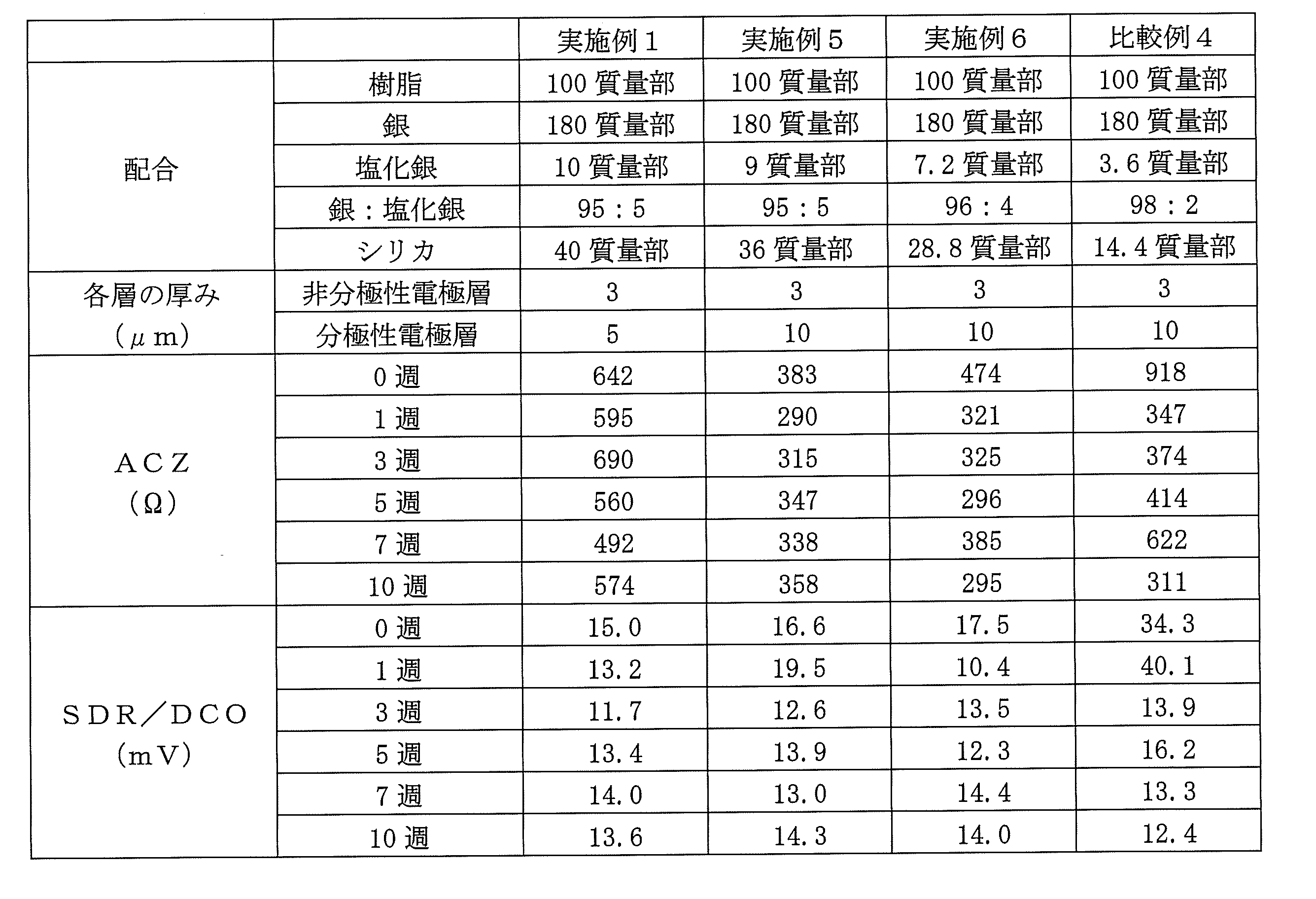
次に、実施例1の配合割合を基準として、非分極性電極層及び分極性電極の厚みについて評価した。結果を表4に示した。非分極性電極層の厚みを2μmとした比較例5は、SDR/DCOが基準を上回り、非分極性電極層の厚みを8μmとした比較例6は、ACZが基準を大きく上回り、電気的な性能が劣っていることが認められた。この結果から、非分極性電極層の厚みは、2μmより大きく、8μm未満であるのが好ましいと考えられる。
また、実施例1及び実施例5の生体用電極のX線撮影を行った結果、X線撮影画像への電極の映り込みは、ほとんど認められなかった。
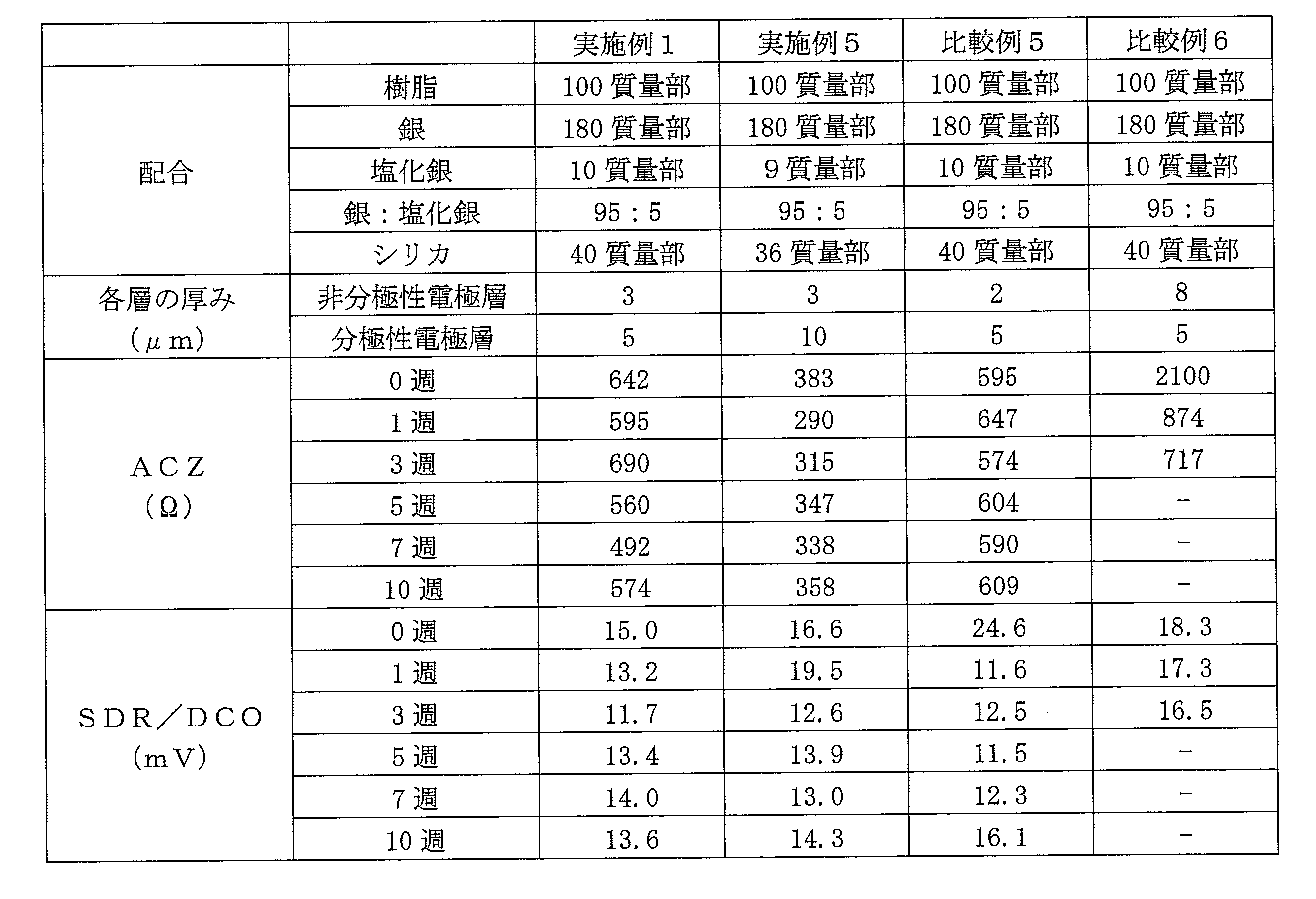
また、上記結果から、分極性電極層の厚みは、ACZの値に大きく寄与することが認められ、特に、この厚みの値が5μmを下回ると、ACZの値が基準を上回る可能性があると考えられる。よって、分極性電極層の厚みは、5μm以上であることが好ましいと考えられる。
1:生体用電極、
10:基材、
20:電極層、22:分極性電極層、24:非分極性電極層、26:導電性ゲル層、
30:リード線
10:基材、
20:電極層、22:分極性電極層、24:非分極性電極層、26:導電性ゲル層、
30:リード線
Claims (3)
- 分極性電極層と、前記分極性電極層に積層された非分極性電極層とを備え、
前記非分極性電極層は、樹脂と、銀と、シリカに担持された塩化銀とを含有し、
前記銀の含有量が、前記樹脂100質量部に対して150~300質量部であり、
前記銀と前記塩化銀との含有量の比率が、97:3~95:5であり、
前記非分極性電極層の厚みが、3~5μmである、生体用電極。 - 前記シリカの含有量が、前記樹脂100質量部に対して20~50質量部である、請求項1に記載の生体用電極。
- 前記分極性電極層の厚みが、5~10μmである、請求項1又は2に記載の生体用電極。
Priority Applications (3)
| Application Number | Priority Date | Filing Date | Title |
|---|---|---|---|
| US17/908,469 US20230108635A1 (en) | 2020-03-13 | 2020-11-10 | Biological electrode |
| JP2022505756A JP7527349B2 (ja) | 2020-03-13 | 2020-11-10 | 生体用電極 |
| CN202080098443.2A CN115279268A (zh) | 2020-03-13 | 2020-11-10 | 生物体用电极 |
Applications Claiming Priority (2)
| Application Number | Priority Date | Filing Date | Title |
|---|---|---|---|
| JP2020-044436 | 2020-03-13 | ||
| JP2020044436 | 2020-03-13 |
Publications (1)
| Publication Number | Publication Date |
|---|---|
| WO2021181752A1 true WO2021181752A1 (ja) | 2021-09-16 |
Family
ID=77671505
Family Applications (1)
| Application Number | Title | Priority Date | Filing Date |
|---|---|---|---|
| PCT/JP2020/041836 Ceased WO2021181752A1 (ja) | 2020-03-13 | 2020-11-10 | 生体用電極 |
Country Status (4)
| Country | Link |
|---|---|
| US (1) | US20230108635A1 (ja) |
| JP (1) | JP7527349B2 (ja) |
| CN (1) | CN115279268A (ja) |
| WO (1) | WO2021181752A1 (ja) |
Families Citing this family (1)
| Publication number | Priority date | Publication date | Assignee | Title |
|---|---|---|---|---|
| US20240407695A1 (en) * | 2021-09-29 | 2024-12-12 | Nitto Denko Corporation | Electrode pad and living body sensor |
Citations (3)
| Publication number | Priority date | Publication date | Assignee | Title |
|---|---|---|---|---|
| JPS55160543A (en) * | 1979-06-04 | 1980-12-13 | Tokuriki Honten Kk | Electrode for drawing minute potential |
| US20050261565A1 (en) * | 2004-05-18 | 2005-11-24 | Micron Medical Products | Discretely coated sensor for use in medical electrodes |
| WO2018003697A1 (ja) * | 2016-06-30 | 2018-01-04 | タツタ電線株式会社 | 生体用電極、及び生体用電極の形成方法 |
Family Cites Families (7)
| Publication number | Priority date | Publication date | Assignee | Title |
|---|---|---|---|---|
| US5265579A (en) * | 1992-09-21 | 1993-11-30 | Ferrari R Keith | X-ray transparent monitoring electrode and method for making |
| JP4171422B2 (ja) * | 2002-01-24 | 2008-10-22 | 久光製薬株式会社 | 電極構造体 |
| JP4624160B2 (ja) * | 2005-04-01 | 2011-02-02 | 石福金属興業株式会社 | 生体用電極 |
| CN107205677B (zh) * | 2015-01-14 | 2020-12-25 | 东洋纺株式会社 | 伸缩性电极片、生物体信息计测用接触面 |
| EP3593714A1 (en) * | 2017-03-07 | 2020-01-15 | Alps Alpine Co., Ltd. | Electrode for biological information measurement and method for producing electrode for biological information measurement |
| JP6654164B2 (ja) * | 2017-03-30 | 2020-02-26 | タツタ電線株式会社 | 塩化銀被覆粒子 |
| JP7158335B2 (ja) * | 2018-06-25 | 2022-10-21 | 信越化学工業株式会社 | 生体電極組成物、生体電極、及び生体電極の製造方法 |
-
2020
- 2020-11-10 US US17/908,469 patent/US20230108635A1/en not_active Abandoned
- 2020-11-10 WO PCT/JP2020/041836 patent/WO2021181752A1/ja not_active Ceased
- 2020-11-10 JP JP2022505756A patent/JP7527349B2/ja active Active
- 2020-11-10 CN CN202080098443.2A patent/CN115279268A/zh active Pending
Patent Citations (3)
| Publication number | Priority date | Publication date | Assignee | Title |
|---|---|---|---|---|
| JPS55160543A (en) * | 1979-06-04 | 1980-12-13 | Tokuriki Honten Kk | Electrode for drawing minute potential |
| US20050261565A1 (en) * | 2004-05-18 | 2005-11-24 | Micron Medical Products | Discretely coated sensor for use in medical electrodes |
| WO2018003697A1 (ja) * | 2016-06-30 | 2018-01-04 | タツタ電線株式会社 | 生体用電極、及び生体用電極の形成方法 |
Also Published As
| Publication number | Publication date |
|---|---|
| JP7527349B2 (ja) | 2024-08-02 |
| JPWO2021181752A1 (ja) | 2021-09-16 |
| US20230108635A1 (en) | 2023-04-06 |
| CN115279268A (zh) | 2022-11-01 |
Similar Documents
| Publication | Publication Date | Title |
|---|---|---|
| Hirata et al. | Thin-film particles of graphite oxide 1:: High-yield synthesis and flexibility of the particles | |
| JP5487502B2 (ja) | 微細炭素繊維水分散液を用いて得られた面状発熱体及びその製造方法 | |
| Wang et al. | Intertwined Nanocarbon and Manganese Oxide Hybrid Foam for High‐Energy Supercapacitors | |
| Nandhini et al. | Supercapacitor electrodes using nanoscale activated carbon from graphite by ball milling | |
| JP7448013B2 (ja) | 生体信号センシング電極 | |
| EP3104150A1 (en) | Sheet for pressure sensor, pressure sensor, and method for producing sheet for pressure sensor | |
| KR20190002447A (ko) | 카본 나노튜브 분산액, 그의 제조 방법 및 도전성 성형체 | |
| Quan et al. | Highly dispersible hexagonal carbon–MoS2–carbon nanoplates with hollow sandwich structures for supercapacitors | |
| Wang et al. | A new ternary composite based on carbon nanotubes/polyindole/graphene with preeminent electrocapacitive performance for supercapacitors | |
| CN114901470A (zh) | 导电性复合结构体及其制造方法 | |
| JP6859083B2 (ja) | 導電性フィルム、及び導電性フィルムの製造方法 | |
| KR20180122320A (ko) | 그래핀 산화물, 이의 제조방법 및 제품 | |
| JP2003238131A (ja) | 炭素からなる骨格を持つ薄膜状粒子のランダム凝集体 | |
| Martin-Gallego et al. | Gold-functionalized graphene as conductive filler in UV-curable epoxy resin | |
| JP7527349B2 (ja) | 生体用電極 | |
| Javanbakht et al. | Rheological and physical properties of a nanocomposite of graphene oxide nanoribbons with polyvinyl alcohol | |
| Wang et al. | Facile synthesis of 3-D composites of MnO2 nanorods and holey graphene oxide for supercapacitors | |
| US12476019B2 (en) | Conductive film and method for producing the same | |
| JP2006063441A (ja) | 金属超微粉スラリー | |
| US20230312865A1 (en) | Electrically conductive compositions | |
| Li et al. | Reduced graphene oxide/MWCNT hybrid sandwiched film by self-assembly for high performance supercapacitor electrodes | |
| US10176932B2 (en) | Method of manufacturing graphene composite including ultrasonic-wave pulverization post-treatment process and method of manufacturing active material using the same | |
| CN111588372A (zh) | 一种制备柔性心电(ecg)电极的方法 | |
| CN113788965A (zh) | 一种细菌纤维素改性巴基纸及其制备方法和应用 | |
| Chekin et al. | Functionalization of Graphene Oxide with 3‐Mercaptopropyltrimethoxysilane and Its Electrocatalytic Activity in Aqueous Medium |
Legal Events
| Date | Code | Title | Description |
|---|---|---|---|
| 121 | Ep: the epo has been informed by wipo that ep was designated in this application |
Ref document number: 20923899 Country of ref document: EP Kind code of ref document: A1 |
|
| ENP | Entry into the national phase |
Ref document number: 2022505756 Country of ref document: JP Kind code of ref document: A |
|
| NENP | Non-entry into the national phase |
Ref country code: DE |
|
| 122 | Ep: pct application non-entry in european phase |
Ref document number: 20923899 Country of ref document: EP Kind code of ref document: A1 |