WO2021181586A1 - シミュレーション装置およびシミュレーションプログラム - Google Patents
シミュレーション装置およびシミュレーションプログラム Download PDFInfo
- Publication number
- WO2021181586A1 WO2021181586A1 PCT/JP2020/010670 JP2020010670W WO2021181586A1 WO 2021181586 A1 WO2021181586 A1 WO 2021181586A1 JP 2020010670 W JP2020010670 W JP 2020010670W WO 2021181586 A1 WO2021181586 A1 WO 2021181586A1
- Authority
- WO
- WIPO (PCT)
- Prior art keywords
- performance
- simulation
- data
- hardware
- various hardware
- Prior art date
- Legal status (The legal status is an assumption and is not a legal conclusion. Google has not performed a legal analysis and makes no representation as to the accuracy of the status listed.)
- Ceased
Links
Images


Classifications
-
- G—PHYSICS
- G06—COMPUTING OR CALCULATING; COUNTING
- G06F—ELECTRIC DIGITAL DATA PROCESSING
- G06F11/00—Error detection; Error correction; Monitoring
- G06F11/30—Monitoring
- G06F11/34—Recording or statistical evaluation of computer activity, e.g. of down time, of input/output operation ; Recording or statistical evaluation of user activity, e.g. usability assessment
Definitions
- This disclosure relates to the realization of a simulation environment that considers hardware performance in model-based development.
- model-based development In the development of various systems, a model for simulating the operation of various systems is used. Development using a model is called model-based development.
- Patent Document 1 discloses a system for model-based development. This system adjusts the simulation execution and display update timing for GUI operations. This makes it possible to check the operation result.
- the purpose of this disclosure is to enable the simulation results to be confirmed at the timing according to the performance of the hardware to be used in the actual machine to be simulated.
- the simulation apparatus of the present disclosure is A model execution unit that executes a simulation model for simulating the execution of target processing by the simulation target, Scheduled performance data showing information for specifying planned performance, which is the performance of various hardware scheduled to be used in the actual machine to be simulated, and standard performance data showing information for specifying standard performance of various hardware.
- Scheduled performance data showing information for specifying planned performance, which is the performance of various hardware scheduled to be used in the actual machine to be simulated
- standard performance data showing information for specifying standard performance of various hardware.
- Reference time data indicating information for specifying the reference time of the target process, which is the time required to execute the target process when the device using various hardware having the reference performance executes the target process.
- a result output unit for reflecting the simulation result on the output of the output device at the adjusted timing is provided.
- FIG. 1 The block diagram of the simulation apparatus 100 in Embodiment 1.
- FIG. 1 The block diagram of the storage part 190 in Embodiment 1.
- FIG. The flowchart of the simulation method in Embodiment 1. The flowchart of the timing adjustment process (S110) in Embodiment 1.
- FIG. 1 The figure which shows the calculation example of the performance difference in Embodiment 1.
- FIG. The figure which shows the calculation example of the reference time in Embodiment 1.
- FIG. 1 The hardware block diagram of the simulation apparatus 100 in Embodiment 1.
- the same element or the corresponding element is designated by the same reference numeral.
- the description of the elements with the same reference numerals as the described elements will be omitted or abbreviated as appropriate.
- the arrows in the figure mainly indicate the flow of data or the flow of processing.
- Embodiment 1 The simulation device 100 will be described with reference to FIGS. 1 to 9.
- the configuration of the simulation device 100 is a computer including hardware such as a processor 101, a memory 102, an auxiliary storage device 103, a communication device 104, and an input / output interface 105. These hardware are connected to each other via signal lines.
- the processor 101 is an IC that performs arithmetic processing and controls other hardware.
- the processor 101 is a CPU, DSP or GPU.
- IC is an abbreviation for Integrated Circuit.
- CPU is an abbreviation for Central Processing Unit.
- DSP is an abbreviation for Digital Signal Processor.
- GPU is an abbreviation for Graphics Processing Unit.
- the memory 102 is a volatile or non-volatile storage device.
- the memory 102 is also called a main storage device or a main memory.
- the memory 102 is a RAM.
- the data stored in the memory 102 is stored in the auxiliary storage device 103 as needed.
- RAM is an abbreviation for Random Access Memory.
- the auxiliary storage device 103 is a non-volatile storage device.
- the auxiliary storage device 103 is a ROM, HDD, or flash memory.
- the data stored in the auxiliary storage device 103 is loaded into the memory 102 as needed.
- ROM is an abbreviation for Read Only Memory.
- HDD is an abbreviation for Hard Disk Drive.
- the communication device 104 is a receiver and a transmitter.
- the communication device 104 is a communication chip or NIC.
- NIC is an abbreviation for Network Interface Card.
- the input / output interface 105 is a port to which the input device and the output device 106 are connected.
- the input / output interface 105 is a USB terminal
- the input device is a keyboard and a mouse
- the output device 106 is a display, a light, a speaker, or the like.
- the output device 106 is also referred to as an actuator.
- a specific example of a display is a liquid crystal panel.
- a specific example of a light is an LED light. LED is an abbreviation for light emitting diode.
- USB is an abbreviation for Universal Serial Bus.
- the simulation device 100 includes elements such as a timing adjustment unit 110, a model execution unit 120, and a result output unit 130.
- the timing adjustment unit 110 includes elements such as a data acquisition unit 111, a delay time calculation unit 112, and a delay time setting unit 113. These elements are realized in software.
- the auxiliary storage device 103 stores a simulation program for operating the computer as the simulation device 100.
- the simulation program is loaded into the memory 102 and executed by the processor 101.
- the OS is further stored in the auxiliary storage device 103. At least part of the OS is loaded into memory 102 and executed by processor 101.
- the processor 101 executes the simulation program while executing the OS.
- OS is an abbreviation for Operating System.
- the input / output data of the simulation program is stored in the storage unit 190.
- the memory 102 functions as a storage unit 190.
- a storage device such as an auxiliary storage device 103, a register in the processor 101, and a cache memory in the processor 101 may function as a storage unit 190 instead of the memory 102 or together with the memory 102.
- the simulation device 100 may include a plurality of processors that replace the processor 101.
- the plurality of processors share the functions of the processor 101.
- the simulation program can be recorded (stored) in a computer-readable manner on a non-volatile recording medium such as an optical disk or a flash memory.
- the configuration of the storage unit 190 will be described with reference to FIG.
- the storage unit 190 stores simulation model 191 and reference performance data 192, reference time data 193, scheduled performance data 194, model setting data 195, and the like.
- the simulation model 191 is a model for simulating the execution of the target process by the simulation target.
- the simulation model 191 is realized by software, hardware or a combination thereof.
- the target process is a process for making the simulation target function.
- the simulation target is a device or program that serves as a human-machine interface.
- human-machine interfaces are various displays provided in the cockpit of an automobile.
- the target process generates images to be displayed on various displays.
- the reference performance data 192 indicates reference performance information.
- the reference performance information is information for specifying the reference performance.
- the reference performance is the performance of various hardware provided in the reference performance device. For example, processor performance is specified by the number of cores, and memory performance is specified by the storage capacity.
- the reference performance device is a device using various hardware having standard performance.
- the reference performance device is realized by a device or a computer that executes a program. For example, reference boards, prototypes or conventional equipment are used as reference performance equipment.
- the reference time data 193 indicates reference time information.
- the reference time information is information for specifying the reference time of the target process.
- the reference time of the target process is the time required to execute the target process when the reference performance device executes the target process.
- execution time The time required for execution is referred to as "execution time”.
- Scheduled performance data 194 indicates scheduled performance information.
- Scheduled performance information is information for specifying scheduled performance.
- the planned performance is the performance of various hardware to be used in the actual machine to be simulated.
- the model setting data 195 indicates setting information for the simulation model 191.
- the setting information for the simulation model 191 is used to specify the influence ratio of various hardware on the execution of the target process.
- the influence ratio is a ratio in which various hardware influences the execution of the target process in a plurality of different types of hardware.
- the total impact rate of various hardware is 100% (%).
- the operation procedure of the simulation device 100 corresponds to the simulation method. Further, the operation procedure of the simulation device 100 corresponds to the processing procedure by the simulation program.
- step S110 the timing adjustment unit 110 adjusts the timing based on various data for timing adjustment.
- Various data for timing adjustment are reference performance data 192, reference time data 193, scheduled performance data 194, and model setting data 195.
- the timing adjustment is a process of adjusting the timing of reflecting the simulation result in the output of the output device 106 according to the scheduled performance of various hardware.
- the simulation result is the result obtained by executing the simulation model 191.
- the simulation result is an image generated by the target process.
- step S111 the data acquisition unit 111 acquires various data for timing adjustment. For example, various data for timing adjustment are input to the simulation device 100. The data acquisition unit 111 receives various data for timing adjustment and stores them in the storage unit 190.
- step S112 the delay time calculation unit 112 calculates the delay time based on various data for timing adjustment.
- the delay time corresponds to the execution time of the target process by various hardware having scheduled performance.
- the delay time calculation unit 112 calculates the delay time as follows.
- the delay time calculation unit 112 specifies the reference time of the target process based on the reference time data 193.
- the delay time calculation unit 112 calculates the performance difference of the planned performance with respect to the standard performance for each type of hardware based on the planned performance data 194 and the reference performance data 192.
- the delay time calculation unit 112 specifies the influence ratio of the target hardware on the target process based on the model setting data 195.
- the target hardware is hardware with different performance.
- the delay time calculation unit 112 calculates the delay time using the reference time of the target process, the performance difference of the target hardware, and the influence ratio of the target hardware on the target process. The details of step S112 will be described later.
- step S113 the delay time setting unit 113 sets the delay time in the result output unit 130.
- the time when the delay time elapses from the execution start time of the simulation model 191 is the timing for reflecting the simulation result in the output of the output device 106.
- step S120 the model execution unit 120 executes the simulation model 191.
- the simulation model 191 is executed as follows. First, the model execution unit 120 acquires the data (processed data) processed by the target process. For example, the processing data is input to the simulation device 100. The model execution unit 120 receives the input processing data and stores it in the storage unit 190. Next, the model execution unit 120 executes the simulation model 191 by inputting the processing data. The data obtained by executing the simulation model 191 is referred to as "result data". The result data shows the simulation results. Then, the model execution unit 120 stores the result data in the storage unit 190.
- the processing data includes the operation command for the indicator, the speed of the automobile, or the image obtained by the in-vehicle camera.
- the simulation result is an image to be displayed on the display in front of the driver's seat, the central display, and the electronic mirror, respectively.
- step S130 the result output unit 130 reflects the simulation result on the output of the output device 106 at the adjustment timing.
- the adjustment timing is the timing adjusted by the timing adjustment in step S110. That is, the adjustment timing is when the delay time has elapsed from the start time of the execution of the simulation model 191.
- the result output unit 130 inputs the result data to the output device 106 at the adjustment timing. Then, the output device 106 reflects the simulation result shown in the result data in the output. For example, the display, which is the output device 106, displays an image included in the simulation result data.
- a plurality of output devices 106 may be connected to the simulation device 100, and the plurality of images may be displayed on different output devices 106. Further, a plurality of images may be displayed on one output device 106.
- the reference performance data 192 shows reference performance values of various hardware.
- the reference performance value is a value representing the performance of various hardware.
- the planned performance data 194 indicates the planned performance values of various hardware.
- the planned performance value is a value representing the performance of various hardware.
- the delay time calculation unit 112 compares the scheduled performance values of the various hardware shown in the scheduled performance data 194 with the reference performance values of the various hardware shown in the reference performance data 192. Then, the delay time calculation unit 112 calculates the performance difference for each type of hardware based on the comparison result.
- the performance difference is the difference in planned performance with respect to the standard performance. In FIG. 5, the planned performance value of the CPU is 50% lower than the reference performance value of the CPU. That is, the performance difference of the CPU is "50%". There is no performance difference between memory, GPU and accelerator.
- the model setting data 195 shows the influence ratio of various hardware on each application.
- the delay time calculation unit 112 identifies the influence ratio of hardware (target hardware) having a performance difference by referring to the model setting data 195.
- the reference time data 193 indicates the reference time of each application.
- the delay time calculation unit 112 specifies the reference time of each application by referring to the reference time data 193.
- the delay time calculation unit 112 calculates the delay time using the reference time of each application, the performance difference of the target hardware, and the influence ratio of the target hardware on each application.
- the reference time of the application A is "100 ms”
- the performance difference of the CPU is "50%”
- the influence ratio of the CPU on the application A is "30%”.
- “50%” means “0.5”
- "30%” means “0.3”
- "100%” means “1”.
- Ms” means milliseconds.
- the delay time calculation unit 112 calculates the delay time for the application A by using "100 ms", “50%”, and “30%”.
- the delay time for application A is "130 ms”.
- the delay time calculation unit 112 further calculates the delay time for each of the applications B and C.
- the performance difference can be calculated by comparing the numerical values.
- the reference performance information and the planned performance information are model identifiers such as the model number of the GPU, it is difficult to calculate the performance difference by comparing the model identifiers with each other.
- the model identifier identifies the model. Different models classify the same type of hardware.
- the difference in model means the difference in performance. Therefore, benchmark data 181 is used.
- the benchmark data 181 is stored in the storage unit 190 in advance. Benchmark data 181 shows the benchmark score for each type of hardware.
- the reference performance data 192 indicates a reference performance value of various hardware or a model identifier of various hardware having the reference performance.
- the planned performance data 194 indicates a planned performance value of various hardware or a model identifier of various hardware having the planned performance.
- the delay time calculation unit 112 acquires the model identifier from each of the reference performance data 192 and the planned performance data 194.
- the model number of the GPU shown in the reference performance data 192 is “XXXX”
- the model number of the GPU shown in the planned performance data 194 is “TTTT”.
- the delay time calculation unit 112 acquires the benchmark score for each model identifier acquired from the reference performance data 192 from the benchmark data 181.
- the acquired benchmark score becomes the standard performance value.
- the delay time calculation unit 112 acquires the benchmark score for each model identifier acquired from the planned performance data 194 from the benchmark data 181.
- the acquired benchmark score becomes the planned performance value.
- the benchmark score of the GPU whose model number is “XXXX”, that is, the reference performance value of the GPU is “8000”.
- the benchmark score of the GPU whose model number is "TTTT”, that is, the planned performance value of the GPU is "4000".
- the delay time calculation unit 112 compares the planned performance values of the various hardware with the reference performance values of the various hardware, and calculates the performance difference for each hardware based on the comparison result.
- the benchmark score “4000”, which is the planned performance value of the GPU is 50% lower than the benchmark score “8000”, which is the reference performance value of the GPU. That is, the performance difference of GPU is "50%".
- the reference time data 193 indicates the reference time of each of the plurality of functional blocks used to execute each application.
- the model configuration data 195 shows a plurality of functional blocks used to execute each application.
- the functional block (A) and the functional block (B) are executed, and the functional block (D) is executed with the output of the functional block (A) and the output of the functional block (B) as inputs. That is, the functional blocks (A), (B) and (D) are used to execute the application A.
- the delay time calculation unit 112 acquires the reference times of the functional blocks (A), (B), and (D) from the reference time data 193, sums the acquired reference times, and calculates the reference time of the application A. ..
- the reference time of the functional blocks (A), (B) and (D) is "50 ms", respectively. Therefore, the reference time of application A is "150 ms”.
- the delay time calculation unit 112 further calculates the reference time for each of the applications B and C.
- the model configuration data 195 shows a plurality of functional blocks used to execute each application. Further, the model setting data 195 shows the influence ratio of various hardware to each functional block.
- the delay time calculation unit 112 acquires the influence ratio of various hardware for each functional block of each application from the model setting data 195. Then, the delay time calculation unit 112 calculates the influence ratio of various hardware on the application by using the acquired influence ratio for each application. For example, the delay time calculation unit 112 calculates the influence ratio of various hardware on the application by summing the acquired influence ratios.
- the simulation device 100 is a simulator used in model-based development, and adjusts the display timing of the simulation result according to the performance of the hardware to be actually used. As a result, not only the verification due to the change of the processing flow in the simulation model 191 but also the verification due to the change of the hardware can be performed.
- the simulation device 100 includes a processing circuit 109.
- the processing circuit 109 is hardware that realizes the timing adjustment unit 110, the model execution unit 120, and the result output unit 130.
- the processing circuit 109 may be dedicated hardware or a processor 101 that executes a program stored in the memory 102.
- the processing circuit 109 is dedicated hardware, the processing circuit 109 is, for example, a single circuit, a composite circuit, a programmed processor, a parallel programmed processor, an ASIC, an FPGA, or a combination thereof.
- ASIC is an abbreviation for Application Special Integrated Circuit.
- FPGA is an abbreviation for Field Programmable Gate Array.
- the simulation device 100 may include a plurality of processing circuits that replace the processing circuit 109.
- the plurality of processing circuits share the functions of the processing circuit 109.
- processing circuit 109 some functions may be realized by dedicated hardware, and the remaining functions may be realized by software or firmware.
- the functions of the simulation device 100 can be realized by hardware, software, firmware, or a combination thereof.
- Embodiment 1 is an example of a preferred embodiment and is not intended to limit the technical scope of the present disclosure. Each embodiment may be partially implemented or may be implemented in combination with other embodiments. The procedure described using the flowchart or the like may be appropriately changed. The "part” which is an element of the simulation apparatus 100 may be read as “processing” or "process”.
- 100 simulation device 101 processor, 102 memory, 103 auxiliary storage device, 104 communication device, 105 input / output interface, 106 output device, 109 processing circuit, 110 timing adjustment unit, 111 data acquisition unit, 112 delay time calculation unit, 113 delay Time setting unit, 120 model execution unit, 130 result output unit, 181 benchmark data, 190 storage unit, 191 simulation model, 192 reference performance data, 193 reference time data, 194 scheduled performance data, 195 model setting data.
Landscapes
- Engineering & Computer Science (AREA)
- General Engineering & Computer Science (AREA)
- Theoretical Computer Science (AREA)
- Computer Hardware Design (AREA)
- Quality & Reliability (AREA)
- Physics & Mathematics (AREA)
- General Physics & Mathematics (AREA)
- Debugging And Monitoring (AREA)
Abstract
モデル実行部(120)は、シミュレーション対象による対象処理の実行をシミュレーションするためのシミュレーションモデルを実行する。タイミング調整部(110)は、前記シミュレーション対象の実機に用いられる予定の各種ハードウェアの性能である予定性能を特定するための情報を示す予定性能データなどに基づいて、シミュレーション結果を出力装置(106)の出力に反映させるタイミングを各種ハードウェアの予定性能に合わせて調整する。結果出力部(130)は、調整されたタイミングに前記シミュレーション結果を前記出力装置の出力に反映させる。
Description
本開示は、モデルベース開発においてハードウェア性能を考慮したシミュレーション環境の実現に関するものである。
各種システムの開発において、各種システムの動作をシミュレーションするためのモデルが用いられる。モデルを用いる開発はモデルベース開発と呼ばれる。
特許文献1は、モデルベース開発のためのシステムを開示している。
このシステムは、GUI操作に対してシミュレーション実行と表示更新タイミングを調整する。これにより、操作結果の確認が可能となる。
このシステムは、GUI操作に対してシミュレーション実行と表示更新タイミングを調整する。これにより、操作結果の確認が可能となる。
従来のモデルベース開発は、シミュレーション対象の実機に用いられるハードウェアが変更されないことを前提にして行われる。つまり、従来のモデルベース開発では、ハードウェアの影響を考慮したシミュレーションが行われない。そのため、ハードウェアが変更される場合には、変更後のハードウェアの性能に応じたタイミングでシミュレーション結果を確認することができない。
本開示は、シミュレーション対象の実機に用いられる予定のハードウェアの性能に応じたタイミングでシミュレーション結果を確認できるようにすることを目的とする。
本開示のシミュレーション装置は、
シミュレーション対象による対象処理の実行をシミュレーションするためのシミュレーションモデルを実行するモデル実行部と、
前記シミュレーション対象の実機に用いられる予定の各種ハードウェアの性能である予定性能を特定するための情報を示す予定性能データと、各種ハードウェアの基準性能を特定するための情報を示す基準性能データと、基準性能を有する各種ハードウェアを用いた装置に前記対象処理を実行させたときに前記対象処理の実行に要した時間である前記対象処理の基準時間を特定するための情報を示す基準時間データと、前記対象処理の実行に対する各種ハードウェアの影響割合を特定するための情報を示すモデル設定データと、に基づいて、前記シミュレーションモデルの実行によって得られるシミュレーション結果を出力装置の出力に反映させるタイミングを各種ハードウェアの予定性能に合わせて調整するタイミング調整部と、
調整されたタイミングに前記シミュレーション結果を前記出力装置の出力に反映させる結果出力部と、を備える。
シミュレーション対象による対象処理の実行をシミュレーションするためのシミュレーションモデルを実行するモデル実行部と、
前記シミュレーション対象の実機に用いられる予定の各種ハードウェアの性能である予定性能を特定するための情報を示す予定性能データと、各種ハードウェアの基準性能を特定するための情報を示す基準性能データと、基準性能を有する各種ハードウェアを用いた装置に前記対象処理を実行させたときに前記対象処理の実行に要した時間である前記対象処理の基準時間を特定するための情報を示す基準時間データと、前記対象処理の実行に対する各種ハードウェアの影響割合を特定するための情報を示すモデル設定データと、に基づいて、前記シミュレーションモデルの実行によって得られるシミュレーション結果を出力装置の出力に反映させるタイミングを各種ハードウェアの予定性能に合わせて調整するタイミング調整部と、
調整されたタイミングに前記シミュレーション結果を前記出力装置の出力に反映させる結果出力部と、を備える。
本開示によれば、シミュレーション対象の実機に用いられる予定のハードウェアの性能に応じたタイミングでシミュレーション結果を確認することが可能となる。
実施の形態および図面において、同じ要素または対応する要素には同じ符号を付している。説明した要素と同じ符号が付された要素の説明は適宜に省略または簡略化する。図中の矢印はデータの流れ又は処理の流れを主に示している。
実施の形態1.
シミュレーション装置100について、図1から図9に基づいて説明する。
シミュレーション装置100について、図1から図9に基づいて説明する。
***構成の説明***
図1に基づいて、シミュレーション装置100の構成を説明する。
シミュレーション装置100は、プロセッサ101とメモリ102と補助記憶装置103と通信装置104と入出力インタフェース105といったハードウェアを備えるコンピュータである。これらのハードウェアは、信号線を介して互いに接続されている。
図1に基づいて、シミュレーション装置100の構成を説明する。
シミュレーション装置100は、プロセッサ101とメモリ102と補助記憶装置103と通信装置104と入出力インタフェース105といったハードウェアを備えるコンピュータである。これらのハードウェアは、信号線を介して互いに接続されている。
プロセッサ101は、演算処理を行うICであり、他のハードウェアを制御する。例えば、プロセッサ101は、CPU、DSPまたはGPUである。
ICは、Integrated Circuitの略称である。
CPUは、Central Processing Unitの略称である。
DSPは、Digital Signal Processorの略称である。
GPUは、Graphics Processing Unitの略称である。
ICは、Integrated Circuitの略称である。
CPUは、Central Processing Unitの略称である。
DSPは、Digital Signal Processorの略称である。
GPUは、Graphics Processing Unitの略称である。
メモリ102は揮発性または不揮発性の記憶装置である。メモリ102は、主記憶装置またはメインメモリとも呼ばれる。例えば、メモリ102はRAMである。メモリ102に記憶されたデータは必要に応じて補助記憶装置103に保存される。
RAMは、Random Access Memoryの略称である。
RAMは、Random Access Memoryの略称である。
補助記憶装置103は不揮発性の記憶装置である。例えば、補助記憶装置103は、ROM、HDDまたはフラッシュメモリである。補助記憶装置103に記憶されたデータは必要に応じてメモリ102にロードされる。
ROMは、Read Only Memoryの略称である。
HDDは、Hard Disk Driveの略称である。
ROMは、Read Only Memoryの略称である。
HDDは、Hard Disk Driveの略称である。
通信装置104はレシーバ及びトランスミッタである。例えば、通信装置104は通信チップまたはNICである。
NICは、Network Interface Cardの略称である。
NICは、Network Interface Cardの略称である。
入出力インタフェース105は、入力装置および出力装置106が接続されるポートである。例えば、入出力インタフェース105はUSB端子であり、入力装置はキーボードおよびマウスであり、出力装置106はディスプレイ、ライトまたはスピーカなどである。出力装置106はアクチュエータともいう。ディスプレイの具体例は液晶パネルである。ライトの具体例はLEDライトである。LEDは発光ダイオードの略称である。
USBは、Universal Serial Busの略称である。
USBは、Universal Serial Busの略称である。
シミュレーション装置100は、タイミング調整部110とモデル実行部120と結果出力部130といった要素を備える。タイミング調整部110は、データ取得部111と遅延時間算出部112と遅延時間設定部113といった要素を備える。これらの要素はソフトウェアで実現される。
補助記憶装置103には、シミュレーション装置100としてコンピュータを機能させるためのシミュレーションプログラムが記憶されている。シミュレーションプログラムは、メモリ102にロードされて、プロセッサ101によって実行される。
補助記憶装置103には、さらに、OSが記憶されている。OSの少なくとも一部は、メモリ102にロードされて、プロセッサ101によって実行される。
プロセッサ101は、OSを実行しながら、シミュレーションプログラムを実行する。
OSは、Operating Systemの略称である。
補助記憶装置103には、さらに、OSが記憶されている。OSの少なくとも一部は、メモリ102にロードされて、プロセッサ101によって実行される。
プロセッサ101は、OSを実行しながら、シミュレーションプログラムを実行する。
OSは、Operating Systemの略称である。
シミュレーションプログラムの入出力データは記憶部190に記憶される。
メモリ102は記憶部190として機能する。但し、補助記憶装置103、プロセッサ101内のレジスタおよびプロセッサ101内のキャッシュメモリなどの記憶装置が、メモリ102の代わりに、又は、メモリ102と共に、記憶部190として機能してもよい。
メモリ102は記憶部190として機能する。但し、補助記憶装置103、プロセッサ101内のレジスタおよびプロセッサ101内のキャッシュメモリなどの記憶装置が、メモリ102の代わりに、又は、メモリ102と共に、記憶部190として機能してもよい。
シミュレーション装置100は、プロセッサ101を代替する複数のプロセッサを備えてもよい。複数のプロセッサは、プロセッサ101の機能を分担する。
シミュレーションプログラムは、光ディスクまたはフラッシュメモリ等の不揮発性の記録媒体にコンピュータ読み取り可能に記録(格納)することができる。
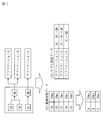
図2に基づいて、記憶部190の構成を説明する。
記憶部190には、シミュレーションモデル191、基準性能データ192、基準時間データ193、予定性能データ194およびモデル設定データ195などが記憶される。
記憶部190には、シミュレーションモデル191、基準性能データ192、基準時間データ193、予定性能データ194およびモデル設定データ195などが記憶される。
シミュレーションモデル191は、シミュレーション対象による対象処理の実行をシミュレーションするためのモデルである。シミュレーションモデル191は、ソフトウェア、ハードウェアまたはこれらの組み合わせで実現される。
対象処理は、シミュレーション対象を機能させるための処理である。
例えば、シミュレーション対象は、ヒューマンマシンインタフェースとなる機器またはプログラムである。ヒューマンマシンインタフェースの具体例は、自動車のコックピットに設けられる各種ディスプレイである。例えば、対象処理は、各種ディスプレイに表示させる画像を生成する。
対象処理は、シミュレーション対象を機能させるための処理である。
例えば、シミュレーション対象は、ヒューマンマシンインタフェースとなる機器またはプログラムである。ヒューマンマシンインタフェースの具体例は、自動車のコックピットに設けられる各種ディスプレイである。例えば、対象処理は、各種ディスプレイに表示させる画像を生成する。
基準性能データ192は、基準性能情報を示す。
基準性能情報は、基準性能を特定するための情報である。
基準性能は、基準性能装置に備わる各種ハードウェアの性能である。例えば、プロセッサの性能はコア数で特定され、メモリの性能は記憶容量で特定される。
基準性能装置は、基準性能を有する各種ハードウェアを用いた装置である。基準性能装置は、機器またはプログラムを実行するコンピュータなどによって実現される。例えば、リファレンスボード、試作品または従来機器などが基準性能装置に使用される。
基準性能情報は、基準性能を特定するための情報である。
基準性能は、基準性能装置に備わる各種ハードウェアの性能である。例えば、プロセッサの性能はコア数で特定され、メモリの性能は記憶容量で特定される。
基準性能装置は、基準性能を有する各種ハードウェアを用いた装置である。基準性能装置は、機器またはプログラムを実行するコンピュータなどによって実現される。例えば、リファレンスボード、試作品または従来機器などが基準性能装置に使用される。
基準時間データ193は、基準時間情報を示す。
基準時間情報は、対象処理の基準時間を特定するための情報である。
対象処理の基準時間は、基準性能装置に対象処理を実行させたときに対象処理の実行に要した時間である。実行に要した時間を「実行時間」と称する。
基準時間情報は、対象処理の基準時間を特定するための情報である。
対象処理の基準時間は、基準性能装置に対象処理を実行させたときに対象処理の実行に要した時間である。実行に要した時間を「実行時間」と称する。
予定性能データ194は、予定性能情報を示す。
予定性能情報は、予定性能を特定するための情報である。
予定性能は、シミュレーション対象の実機に用いられる予定の各種ハードウェアの性能である。
予定性能情報は、予定性能を特定するための情報である。
予定性能は、シミュレーション対象の実機に用いられる予定の各種ハードウェアの性能である。
モデル設定データ195は、シミュレーションモデル191に対する設定情報を示す。
シミュレーションモデル191に対する設定情報は、対象処理の実行に対する各種ハードウェアの影響割合を特定するために用いられる。
影響割合は、種類が異なる複数のハードウェアにおいて各種ハードウェアが対象処理の実行に影響を与える割合である。各種ハードウェアの影響割合の合計は100パーセント(%)である。
シミュレーションモデル191に対する設定情報は、対象処理の実行に対する各種ハードウェアの影響割合を特定するために用いられる。
影響割合は、種類が異なる複数のハードウェアにおいて各種ハードウェアが対象処理の実行に影響を与える割合である。各種ハードウェアの影響割合の合計は100パーセント(%)である。
***動作の説明***
シミュレーション装置100の動作の手順はシミュレーション方法に相当する。また、シミュレーション装置100の動作の手順はシミュレーションプログラムによる処理の手順に相当する。
シミュレーション装置100の動作の手順はシミュレーション方法に相当する。また、シミュレーション装置100の動作の手順はシミュレーションプログラムによる処理の手順に相当する。
図3に基づいて、シミュレーション方法を説明する。
ステップS110において、タイミング調整部110は、タイミング調整用の各種データに基づいてタイミング調整を行う。
タイミング調整用の各種データは、基準性能データ192と基準時間データ193と予定性能データ194とモデル設定データ195である。
タイミング調整は、シミュレーション結果を出力装置106の出力に反映させるタイミングを各種ハードウェアの予定性能に合わせて調整する処理である。
シミュレーション結果は、シミュレーションモデル191の実行によって得られる結果である。例えば、シミュレーション結果は対象処理によって生成される画像である。
ステップS110において、タイミング調整部110は、タイミング調整用の各種データに基づいてタイミング調整を行う。
タイミング調整用の各種データは、基準性能データ192と基準時間データ193と予定性能データ194とモデル設定データ195である。
タイミング調整は、シミュレーション結果を出力装置106の出力に反映させるタイミングを各種ハードウェアの予定性能に合わせて調整する処理である。
シミュレーション結果は、シミュレーションモデル191の実行によって得られる結果である。例えば、シミュレーション結果は対象処理によって生成される画像である。
図4に基づいて、タイミング調整処理(S110)の手順を説明する。
ステップS111において、データ取得部111は、タイミング調整用の各種データを取得する。
例えば、タイミング調整用の各種データがシミュレーション装置100に入力される。データ取得部111は、タイミング調整用の各種データを受け付けて記憶部190に記憶する。
ステップS111において、データ取得部111は、タイミング調整用の各種データを取得する。
例えば、タイミング調整用の各種データがシミュレーション装置100に入力される。データ取得部111は、タイミング調整用の各種データを受け付けて記憶部190に記憶する。
ステップS112において、遅延時間算出部112は、タイミング調整用の各種データに基づいて遅延時間を算出する。
遅延時間は、予定性能を有する各種ハードウェアによる対象処理の実行時間に相当する。
遅延時間は、予定性能を有する各種ハードウェアによる対象処理の実行時間に相当する。
遅延時間算出部112は、遅延時間を以下のように算出する。
遅延時間算出部112は、基準時間データ193に基づいて、対象処理の基準時間を特定する。
遅延時間算出部112は、予定性能データ194と基準性能データ192とに基づいて、ハードウェアの種類毎に基準性能に対する予定性能の性能差を算出する。
遅延時間算出部112は、モデル設定データ195に基づいて、対象処理に対する対象ハードウェアの影響割合を特定する。対象ハードウェアは、性能差があるハードウェアである。
そして、遅延時間算出部112は、対象処理の基準時間と、対象ハードウェアの性能差と、対象処理に対する対象ハードウェアの影響割合と、を用いて遅延時間を算出する。
ステップS112の詳細について後述する。
遅延時間算出部112は、基準時間データ193に基づいて、対象処理の基準時間を特定する。
遅延時間算出部112は、予定性能データ194と基準性能データ192とに基づいて、ハードウェアの種類毎に基準性能に対する予定性能の性能差を算出する。
遅延時間算出部112は、モデル設定データ195に基づいて、対象処理に対する対象ハードウェアの影響割合を特定する。対象ハードウェアは、性能差があるハードウェアである。
そして、遅延時間算出部112は、対象処理の基準時間と、対象ハードウェアの性能差と、対象処理に対する対象ハードウェアの影響割合と、を用いて遅延時間を算出する。
ステップS112の詳細について後述する。
ステップS113において、遅延時間設定部113は、遅延時間を結果出力部130に設定する。
シミュレーションモデル191の実行の開始時刻から遅延時間が経過したときが、シミュレーション結果を出力装置106の出力に反映させるタイミングである。
シミュレーションモデル191の実行の開始時刻から遅延時間が経過したときが、シミュレーション結果を出力装置106の出力に反映させるタイミングである。
図3に戻り、ステップS120から説明を続ける。
ステップS120において、モデル実行部120は、シミュレーションモデル191を実行する。
ステップS120において、モデル実行部120は、シミュレーションモデル191を実行する。
シミュレーションモデル191は、以下のように実行される。
まず、モデル実行部120は、対象処理によって処理されるデータ(処理データ)を取得する。例えば、処理データがシミュレーション装置100に入力される。モデル実行部120は、入力された処理データを受け付けて記憶部190に記憶する。
次に、モデル実行部120は、処理データを入力にしてシミュレーションモデル191を実行する。シミュレーションモデル191の実行によって得られるデータを「結果データ」と称する。結果データはシミュレーション結果を示す。
そして、モデル実行部120は、結果データを記憶部190に記憶する。
まず、モデル実行部120は、対象処理によって処理されるデータ(処理データ)を取得する。例えば、処理データがシミュレーション装置100に入力される。モデル実行部120は、入力された処理データを受け付けて記憶部190に記憶する。
次に、モデル実行部120は、処理データを入力にしてシミュレーションモデル191を実行する。シミュレーションモデル191の実行によって得られるデータを「結果データ」と称する。結果データはシミュレーション結果を示す。
そして、モデル実行部120は、結果データを記憶部190に記憶する。
シミュレーション対象が自動車のコックピットに設けられる各種ディスプレイである場合、指示器に対する操作コマンド、自動車の速度または車載カメラによって得られる映像などが処理データとなる。例えば、シミュレーション結果は、運転席前のディスプレイと中央のディスプレイと電子ミラーとのそれぞれに表示させる画像である。
ステップS130において、結果出力部130は、調整タイミングにシミュレーション結果を出力装置106の出力に反映させる。
調整タイミングは、ステップS110におけるタイミング調整によって調整されたタイミングである。つまり、調整タイミングは、シミュレーションモデル191の実行の開始時刻から遅延時間が経過したときである。
調整タイミングは、ステップS110におけるタイミング調整によって調整されたタイミングである。つまり、調整タイミングは、シミュレーションモデル191の実行の開始時刻から遅延時間が経過したときである。
具体的には、結果出力部130は、調整タイミングに出力装置106に結果データを入力する。そして、出力装置106は、結果データに示されるシミュレーション結果を出力に反映させる。
例えば、出力装置106であるディスプレイは、シミュレーション結果データに含まれる画像を表示する。
例えば、出力装置106であるディスプレイは、シミュレーション結果データに含まれる画像を表示する。
シミュレーションモデル191の実行によって複数の画像が得られる場合、複数の出力装置106がシミュレーション装置100に接続され、複数の画像が互いに異なる出力装置106に表示されてもよい。また、複数の画像が1つの出力装置106に表示されてもよい。
図5から図8に基づいて、遅延時間算出処理(S112)について説明する。
アプリケーションA~Cは、互いに異なる対象処理を実行するためのソフトウェアである。つまり、1つのアプリケーションの実行は1つの対象処理の実行を意味する。「アプリケーション」は「対象処理」と読み替えることができる。
アプリケーションA~Cは、互いに異なる対象処理を実行するためのソフトウェアである。つまり、1つのアプリケーションの実行は1つの対象処理の実行を意味する。「アプリケーション」は「対象処理」と読み替えることができる。
図5に基づいて、遅延時間の算出例を説明する。
基準性能データ192は、各種ハードウェアの基準性能値を示す。基準性能値は、各種ハードウェアの性能を表す値である。
予定性能データ194は、各種ハードウェアの予定性能値を示す。予定性能値は、各種ハードウェアの性能を表す値である。
基準性能データ192は、各種ハードウェアの基準性能値を示す。基準性能値は、各種ハードウェアの性能を表す値である。
予定性能データ194は、各種ハードウェアの予定性能値を示す。予定性能値は、各種ハードウェアの性能を表す値である。
遅延時間算出部112は、予定性能データ194に示される各種ハードウェアの予定性能値を基準性能データ192に示される各種ハードウェアの基準性能値と比較する。そして、遅延時間算出部112は、ハードウェアの種類毎に比較結果に基づいて性能差を算出する。性能差は、基準性能に対する予定性能の差である。
図5において、CPUの予定性能値がCPUの基準性能値から50パーセントダウンしている。つまり、CPUの性能差は「50%」である。メモリとGPUとアクセラレータについては性能差がない。
図5において、CPUの予定性能値がCPUの基準性能値から50パーセントダウンしている。つまり、CPUの性能差は「50%」である。メモリとGPUとアクセラレータについては性能差がない。
モデル設定データ195は、各アプリケーションに対する各種ハードウェアの影響割合を示す。
遅延時間算出部112は、モデル設定データ195を参照することによって、性能差があるハードウェア(対象ハードウェア)の影響割合を特定する。
基準時間データ193は、各アプリケーションの基準時間を示す。
遅延時間算出部112は、基準時間データ193を参照することによって各アプリケーションの基準時間を特定する。
そして、遅延時間算出部112は、各アプリケーションの基準時間と、対象ハードウェアの性能差と、各アプリケーションに対する対象ハードウェアの影響割合と、を用いて遅延時間を算出する。
図5において、アプリケーションAの基準時間は「100ms」であり、CPUの性能差は「50%」であり、アプリケーションAに対するCPUの影響割合は「30%」である。「50%」は「0.5」を意味し、「30%」は「0.3」を意味し、「100%」は「1」を意味する。「ms」はミリ秒を意味する。
遅延時間算出部112は、「100ms」と「50%」と「30%」とを用いて、アプリケーションAに対する遅延時間を算出する。アプリケーションAに対する遅延時間は「130ms」である。
遅延時間算出部112は、さらに、アプリケーションB,Cのそれぞれに対する遅延時間を算出する。
図5において、アプリケーションAの基準時間は「100ms」であり、CPUの性能差は「50%」であり、アプリケーションAに対するCPUの影響割合は「30%」である。「50%」は「0.5」を意味し、「30%」は「0.3」を意味し、「100%」は「1」を意味する。「ms」はミリ秒を意味する。
遅延時間算出部112は、「100ms」と「50%」と「30%」とを用いて、アプリケーションAに対する遅延時間を算出する。アプリケーションAに対する遅延時間は「130ms」である。
遅延時間算出部112は、さらに、アプリケーションB,Cのそれぞれに対する遅延時間を算出する。
遅延時間は以下の式で表すことができる。
遅延時間 = 基準時間 * (非影響割合 + 影響度)
非影響割合 = 1 - 影響割合
影響度 = 影響割合 / 性能差
遅延時間 = 基準時間 * (非影響割合 + 影響度)
非影響割合 = 1 - 影響割合
影響度 = 影響割合 / 性能差
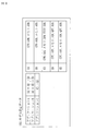
図6に基づいて、性能差の算出例を説明する。
基準性能情報および予定性能情報がCPUのコア数のような数値である場合、数値同士を比較することによって性能差を算出することができる。
しかし、基準性能情報および予定性能情報がGPUの型番のような型式識別子である場合、型式識別子同士を比較することによって性能差を算出することは難しい。型式識別子は型式を識別する。異なる型式は、同じ種類のハードウェアを分類する。型式の違いは性能の違いを意味する。
そこで、ベンチマークデータ181が使用される。例えば、ベンチマークデータ181は記憶部190に予め記憶される。
ベンチマークデータ181は、各種ハードウェアの型式ごとにベンチマークスコアを示す。
基準性能情報および予定性能情報がCPUのコア数のような数値である場合、数値同士を比較することによって性能差を算出することができる。
しかし、基準性能情報および予定性能情報がGPUの型番のような型式識別子である場合、型式識別子同士を比較することによって性能差を算出することは難しい。型式識別子は型式を識別する。異なる型式は、同じ種類のハードウェアを分類する。型式の違いは性能の違いを意味する。
そこで、ベンチマークデータ181が使用される。例えば、ベンチマークデータ181は記憶部190に予め記憶される。
ベンチマークデータ181は、各種ハードウェアの型式ごとにベンチマークスコアを示す。
基準性能データ192は、各種ハードウェアの基準性能値または基準性能を有する各種ハードウェアの型式識別子を示す。
予定性能データ194は、各種ハードウェアの予定性能値または予定性能を有する各種ハードウェアの型式識別子を示す。
予定性能データ194は、各種ハードウェアの予定性能値または予定性能を有する各種ハードウェアの型式識別子を示す。
まず、遅延時間算出部112は、基準性能データ192と予定性能データ194のそれぞれから型式識別子を取得する。
図6において、基準性能データ192に示されるGPUの型番は「XXXX」であり、予定性能データ194に示されるGPUの型番は「TTTT」である。
図6において、基準性能データ192に示されるGPUの型番は「XXXX」であり、予定性能データ194に示されるGPUの型番は「TTTT」である。
次に、遅延時間算出部112は、基準性能データ192から取得した各型式識別子に対するベンチマークスコアをベンチマークデータ181から取得する。取得されるベンチマークスコアが基準性能値となる。
また、遅延時間算出部112は、予定性能データ194から取得した各型式識別子に対するベンチマークスコアをベンチマークデータ181から取得する。取得されるベンチマークスコアが予定性能値となる。
図6において、型番が「XXXX」であるGPUのベンチマークスコアすなわちGPUの基準性能値は「8000」である。また、型番が「TTTT」であるGPUのベンチマークスコアすなわちGPUの予定性能値は「4000」である。
また、遅延時間算出部112は、予定性能データ194から取得した各型式識別子に対するベンチマークスコアをベンチマークデータ181から取得する。取得されるベンチマークスコアが予定性能値となる。
図6において、型番が「XXXX」であるGPUのベンチマークスコアすなわちGPUの基準性能値は「8000」である。また、型番が「TTTT」であるGPUのベンチマークスコアすなわちGPUの予定性能値は「4000」である。
そして、遅延時間算出部112は、各種ハードウェアの予定性能値を各種ハードウェアの基準性能値と比較し、ハードウェア毎に比較結果に基づいて性能差を算出する。
図6において、GPUの予定性能値であるベンチマークスコア「4000」はGPUの基準性能値であるベンチマークスコア「8000」から50%ダウンしている。つまり、GPUの性能差は「50%」である。
図6において、GPUの予定性能値であるベンチマークスコア「4000」はGPUの基準性能値であるベンチマークスコア「8000」から50%ダウンしている。つまり、GPUの性能差は「50%」である。
図7に基づいて、各アプリケーションが複数の機能ブロックで実現される場合における各アプリケーションの基準時間の算出例を説明する。
基準時間データ193は、各アプリケーションを実行するために使用される複数の機能ブロックのそれぞれの基準時間を示している。
モデル設定データ195は、各アプリケーションを実行するために使用される複数の機能ブロックを示している。
アプリケーションAにおいて、機能ブロック(A)と機能ブロック(B)が実行され、機能ブロック(A)の出力と機能ブロック(B)の出力とを入力として機能ブロック(D)が実行される。つまり、アプリケーションAを実行するために、機能ブロック(A)、(B)および(D)が使用される。
遅延時間算出部112は、機能ブロック(A)、(B)および(D)のそれぞれの基準時間を基準時間データ193から取得し、取得した基準時間を合計してアプリケーションAの基準時間を算出する。
機能ブロック(A)、(B)および(D)の基準時間はそれぞれ「50ms」である。したがって、アプリケーションAの基準時間は「150ms」である。
遅延時間算出部112は、さらに、アプリケーションB,Cのそれぞれの基準時間を算出する。
基準時間データ193は、各アプリケーションを実行するために使用される複数の機能ブロックのそれぞれの基準時間を示している。
モデル設定データ195は、各アプリケーションを実行するために使用される複数の機能ブロックを示している。
アプリケーションAにおいて、機能ブロック(A)と機能ブロック(B)が実行され、機能ブロック(A)の出力と機能ブロック(B)の出力とを入力として機能ブロック(D)が実行される。つまり、アプリケーションAを実行するために、機能ブロック(A)、(B)および(D)が使用される。
遅延時間算出部112は、機能ブロック(A)、(B)および(D)のそれぞれの基準時間を基準時間データ193から取得し、取得した基準時間を合計してアプリケーションAの基準時間を算出する。
機能ブロック(A)、(B)および(D)の基準時間はそれぞれ「50ms」である。したがって、アプリケーションAの基準時間は「150ms」である。
遅延時間算出部112は、さらに、アプリケーションB,Cのそれぞれの基準時間を算出する。
図8に基づいて、各アプリケーションが複数の機能ブロックで実現される場合における各アプリケーションに対する各ハードウェアの影響割合の算出について説明する。
モデル設定データ195は、各アプリケーションを実行するために使用される複数の機能ブロックを示している。さらに、モデル設定データ195は、各機能ブロックに対する各種ハードウェアの影響割合を示している。
遅延時間算出部112は、各アプリケーションの機能ブロックごとに各種ハードウェアの影響割合をモデル設定データ195から取得する。そして、遅延時間算出部112は、アプリケーションごとに、取得した影響割合を用いてアプリケーションに対する各種ハードウェアの影響割合を算出する。例えば、遅延時間算出部112は、取得した影響割合を合計してアプリケーションに対する各種ハードウェアの影響割合を算出する。
モデル設定データ195は、各アプリケーションを実行するために使用される複数の機能ブロックを示している。さらに、モデル設定データ195は、各機能ブロックに対する各種ハードウェアの影響割合を示している。
遅延時間算出部112は、各アプリケーションの機能ブロックごとに各種ハードウェアの影響割合をモデル設定データ195から取得する。そして、遅延時間算出部112は、アプリケーションごとに、取得した影響割合を用いてアプリケーションに対する各種ハードウェアの影響割合を算出する。例えば、遅延時間算出部112は、取得した影響割合を合計してアプリケーションに対する各種ハードウェアの影響割合を算出する。
***実施の形態1の効果***
シミュレーション装置100は、モデルベース開発で用いるシミュレータであり、実際に用いられる予定のハードウェアの性能に応じて、シミュレーション結果の表示タイミングを調整する。これにより、シミュレーションモデル191の中の処理フローの変更に伴う検証だけでなく、ハードウェアの変更に伴う検証を行うことができる。
シミュレーション装置100は、モデルベース開発で用いるシミュレータであり、実際に用いられる予定のハードウェアの性能に応じて、シミュレーション結果の表示タイミングを調整する。これにより、シミュレーションモデル191の中の処理フローの変更に伴う検証だけでなく、ハードウェアの変更に伴う検証を行うことができる。
***実施の形態1の補足***
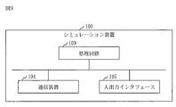
図9に基づいて、シミュレーション装置100のハードウェア構成を説明する。
シミュレーション装置100は処理回路109を備える。
処理回路109は、タイミング調整部110とモデル実行部120と結果出力部130とを実現するハードウェアである。
処理回路109は、専用のハードウェアであってもよいし、メモリ102に格納されるプログラムを実行するプロセッサ101であってもよい。
図9に基づいて、シミュレーション装置100のハードウェア構成を説明する。
シミュレーション装置100は処理回路109を備える。
処理回路109は、タイミング調整部110とモデル実行部120と結果出力部130とを実現するハードウェアである。
処理回路109は、専用のハードウェアであってもよいし、メモリ102に格納されるプログラムを実行するプロセッサ101であってもよい。
処理回路109が専用のハードウェアである場合、処理回路109は、例えば、単一回路、複合回路、プログラム化したプロセッサ、並列プログラム化したプロセッサ、ASIC、FPGAまたはこれらの組み合わせである。
ASICは、Application Specific Integrated Circuitの略称である。
FPGAは、Field Programmable Gate Arrayの略称である。
ASICは、Application Specific Integrated Circuitの略称である。
FPGAは、Field Programmable Gate Arrayの略称である。
シミュレーション装置100は、処理回路109を代替する複数の処理回路を備えてもよい。複数の処理回路は、処理回路109の機能を分担する。
処理回路109において、一部の機能が専用のハードウェアで実現されて、残りの機能がソフトウェアまたはファームウェアで実現されてもよい。
このように、シミュレーション装置100の機能はハードウェア、ソフトウェア、ファームウェアまたはこれらの組み合わせで実現することができる。
実施の形態1は、好ましい形態の例示であり、本開示の技術的範囲を制限することを意図するものではない。各実施の形態は、部分的に実施してもよいし、他の形態と組み合わせて実施してもよい。フローチャート等を用いて説明した手順は、適宜に変更してもよい。
シミュレーション装置100の要素である「部」は、「処理」または「工程」と読み替えてもよい。
シミュレーション装置100の要素である「部」は、「処理」または「工程」と読み替えてもよい。
100 シミュレーション装置、101 プロセッサ、102 メモリ、103 補助記憶装置、104 通信装置、105 入出力インタフェース、106 出力装置、109 処理回路、110 タイミング調整部、111 データ取得部、112 遅延時間算出部、113 遅延時間設定部、120 モデル実行部、130 結果出力部、181 ベンチマークデータ、190 記憶部、191 シミュレーションモデル、192 基準性能データ、193 基準時間データ、194 予定性能データ、195 モデル設定データ。
Claims (9)
- シミュレーション対象による対象処理の実行をシミュレーションするためのシミュレーションモデルを実行するモデル実行部と、
前記シミュレーション対象の実機に用いられる予定の各種ハードウェアの性能である予定性能を特定するための情報を示す予定性能データと、各種ハードウェアの基準性能を特定するための情報を示す基準性能データと、基準性能を有する各種ハードウェアを用いた装置に前記対象処理を実行させたときに前記対象処理の実行に要した時間である前記対象処理の基準時間を特定するための情報を示す基準時間データと、前記対象処理の実行に対する各種ハードウェアの影響割合を特定するための情報を示すモデル設定データと、に基づいて、前記シミュレーションモデルの実行によって得られるシミュレーション結果を出力装置の出力に反映させるタイミングを各種ハードウェアの予定性能に合わせて調整するタイミング調整部と、
調整されたタイミングに前記シミュレーション結果を前記出力装置の出力に反映させる結果出力部と、
を備えるシミュレーション装置。 - 前記タイミング調整部は、
前記基準時間データに基づいて、前記対象処理の前記基準時間を特定し、
前記予定性能データと前記基準性能データとに基づいて、ハードウェアの種類毎に基準性能に対する予定性能の性能差を算出し、
前記モデル設定データに基づいて、性能差があるハードウェアである対象ハードウェアの前記対象処理に対する影響割合を特定し、
前記対象処理の前記基準時間と、前記対象ハードウェアの性能差と、前記対象処理に対する前記対象ハードウェアの影響割合と、を用いて、予定性能を有する各種ハードウェアによる前記対象処理の実行時間を遅延時間として算出し、
前記調整されたタイミングが、前記シミュレーションモデルの実行の開始時刻から前記遅延時間が経過したときである
請求項1に記載のシミュレーション装置。 - 前記基準時間データは、前記対象処理の前記基準時間を示し、
前記タイミング調整部は、前記基準時間データを参照することによって前記対象処理の前記基準時間を特定する
請求項2に記載のシミュレーション装置。 - 前記基準時間データは、前記対象処理を実行するために使用される複数の機能ブロックのそれぞれの基準時間を示し、
前記タイミング調整部は、前記基準時間データから前記複数の機能ブロックのそれぞれの基準時間を取得し、取得した基準時間を合計して前記対象処理の前記基準時間を算出する
請求項2に記載のシミュレーション装置。 - 前記基準性能データは、各種ハードウェアの基準性能を表す基準性能値を示し、
前記予定性能データは、各種ハードウェアの予定性能を表す予定性能値を示し、
前記タイミング調整部は、
前記予定性能データに示される各種ハードウェアの予定性能値を前記基準性能データに示される各種ハードウェアの基準性能値と比較し、ハードウェアの種類毎に基準性能に対する予定性能の性能差を比較結果に基づいて算出する
請求項2から請求項4のいずれか1項に記載のシミュレーション装置。 - 前記基準性能データは、各種ハードウェアの基準性能を表す基準性能値または基準性能を有する各種ハードウェアの型式識別子を示し、
前記予定性能データは、各種ハードウェアの予定性能を表す予定性能値または予定性能を有する各種ハードウェアの型式識別子を示し、
前記タイミング調整部は、各種ハードウェアの型式識別子ごとにベンチマークスコアを示すベンチマークデータから前記基準性能データに示される各型式識別子に対応するベンチマークスコアを基準性能値として取得し、前記ベンチマークデータから前記予定性能データに示される各型式識別子に対応するベンチマークスコアを予定性能値として取得し、各種ハードウェアの予定性能値を各種ハードウェアの基準性能値と比較し、ハードウェアの種類毎に基準性能に対する予定性能の性能差を比較結果に基づいて算出する
請求項2から請求項4のいずれか1項に記載のシミュレーション装置。 - 前記モデル設定データは、前記対象処理に対する各種ハードウェアの影響割合を示し、
前記タイミング調整部は、
前記モデル設定データを参照することによって前記対象処理に対する前記対象ハードウェアの前記影響割合を特定する
請求項2から請求項6のいずれか1項に記載のシミュレーション装置。 - モデル設定データは、前記対象処理を実行するために使用される複数の機能ブロックのそれぞれに対する各種ハードウェアの影響割合を示し、
タイミング調整部は、
前記対象ハードウェアの影響割合を前記モデル設定データから機能ブロックごとに取得し、取得した影響割合を用いて前記対象処理に対する前記対象ハードウェアの前記影響割合を算出する
請求項2から請求項6のいずれか1項に記載のシミュレーション装置。 - シミュレーション対象による対象処理の実行をシミュレーションするためのシミュレーションモデルを実行するモデル実行処理と、
前記シミュレーション対象の実機に用いられる予定の各種ハードウェアの性能である予定性能を特定するための情報を示す予定性能データと、各種ハードウェアの基準性能を特定するための情報を示す基準性能データと、基準性能を有する各種ハードウェアを用いた装置に前記対象処理を実行させたときに前記対象処理の実行に要した時間である前記対象処理の基準時間を特定するための情報を示す基準時間データと、前記対象処理の実行に対する各種ハードウェアの影響割合を特定するための情報を示すモデル設定データと、に基づいて、前記シミュレーションモデルの実行によって得られるシミュレーション結果を出力装置の出力に反映させるタイミングを各種ハードウェアの予定性能に合わせて調整するタイミング調整処理と、
調整されたタイミングに前記シミュレーション結果を前記出力装置の出力に反映させる結果出力処理と、
をコンピュータに実行させるためのシミュレーションプログラム。
Priority Applications (1)
| Application Number | Priority Date | Filing Date | Title |
|---|---|---|---|
| PCT/JP2020/010670 WO2021181586A1 (ja) | 2020-03-11 | 2020-03-11 | シミュレーション装置およびシミュレーションプログラム |
Applications Claiming Priority (1)
| Application Number | Priority Date | Filing Date | Title |
|---|---|---|---|
| PCT/JP2020/010670 WO2021181586A1 (ja) | 2020-03-11 | 2020-03-11 | シミュレーション装置およびシミュレーションプログラム |
Publications (1)
| Publication Number | Publication Date |
|---|---|
| WO2021181586A1 true WO2021181586A1 (ja) | 2021-09-16 |
Family
ID=77670558
Family Applications (1)
| Application Number | Title | Priority Date | Filing Date |
|---|---|---|---|
| PCT/JP2020/010670 Ceased WO2021181586A1 (ja) | 2020-03-11 | 2020-03-11 | シミュレーション装置およびシミュレーションプログラム |
Country Status (1)
| Country | Link |
|---|---|
| WO (1) | WO2021181586A1 (ja) |
Citations (3)
| Publication number | Priority date | Publication date | Assignee | Title |
|---|---|---|---|---|
| JP2004258705A (ja) * | 2003-02-24 | 2004-09-16 | Hitachi Ltd | プログラム処理時間推定方法 |
| JP2007334812A (ja) * | 2006-06-19 | 2007-12-27 | Nec Electronics Corp | シミュレータ及びシミュレーション方法 |
| JP2018022424A (ja) * | 2016-08-05 | 2018-02-08 | 株式会社日立製作所 | システム開発支援装置およびシステム開発支援方法 |
-
2020
- 2020-03-11 WO PCT/JP2020/010670 patent/WO2021181586A1/ja not_active Ceased
Patent Citations (3)
| Publication number | Priority date | Publication date | Assignee | Title |
|---|---|---|---|---|
| JP2004258705A (ja) * | 2003-02-24 | 2004-09-16 | Hitachi Ltd | プログラム処理時間推定方法 |
| JP2007334812A (ja) * | 2006-06-19 | 2007-12-27 | Nec Electronics Corp | シミュレータ及びシミュレーション方法 |
| JP2018022424A (ja) * | 2016-08-05 | 2018-02-08 | 株式会社日立製作所 | システム開発支援装置およびシステム開発支援方法 |
Similar Documents
| Publication | Publication Date | Title |
|---|---|---|
| US9921949B2 (en) | Software testing | |
| US20090049214A1 (en) | Graphics card test method | |
| CN114328045B (zh) | 一种bmc的i2c调试方法、系统、装置及计算机可读存储介质 | |
| CN113272785B (zh) | 一种挂载文件系统的方法、终端设备及存储介质 | |
| US10606970B2 (en) | Selection of corners and/or margins using statistical static timing analysis of an integrated circuit | |
| US12106455B2 (en) | Autonomous vehicle system testing simulator | |
| JP7441981B2 (ja) | 切り替え可能モデルを有する自律運転シミュレーションアーキテクチャを提供するためのシステムと方法 | |
| CN118887071B (zh) | Gpu图元预处理装置、系统及方法 | |
| JP2017084082A (ja) | シミュレーション装置、試験シナリオファイル作成方法、及び試験シナリオファイルを用いた試験方法 | |
| CN110941934A (zh) | 一种fpga原型验证开发板分割仿真系统、方法、介质及终端 | |
| AU2017438670B2 (en) | Simulation device, simulation method, and simulation program | |
| US20180039242A1 (en) | Hil simulation system and control method of the same | |
| US9280627B1 (en) | GUI based verification at multiple abstraction levels | |
| WO2021181586A1 (ja) | シミュレーション装置およびシミュレーションプログラム | |
| CN118860495A (zh) | Gpu指令处理前端模拟装置、系统、方法以及存储介质 | |
| CN109716304B (zh) | 用于测试混合指令体系结构的方法和系统 | |
| US9710581B1 (en) | VIP assisted method and apparatus to enable SOC integration and software development | |
| JP5011221B2 (ja) | コントローラ開発ツールとそれを利用して開発したモータドライブシステムを有する機器 | |
| CN112596869A (zh) | 延时模型的构建方法及装置、电子设备及存储介质 | |
| US20150026652A1 (en) | System, method, and computer program product for correlating transactions within a simulation of a hardware platform for post-simulation debugging | |
| JP5530417B2 (ja) | コントローラ開発ツール | |
| JP2921087B2 (ja) | ハードウェアアクセラレータにおける実チップシミュレーション方式 | |
| WO2024004203A1 (ja) | 保守支援システム、保守支援方法、および、保守支援プログラム | |
| CN118708480A (zh) | 数据处理方法、装置以及电子设备 | |
| CN120951895A (zh) | 芯片后仿方法、装置、电子设备、介质及芯片 |
Legal Events
| Date | Code | Title | Description |
|---|---|---|---|
| 121 | Ep: the epo has been informed by wipo that ep was designated in this application |
Ref document number: 20924245 Country of ref document: EP Kind code of ref document: A1 |
|
| NENP | Non-entry into the national phase |
Ref country code: DE |
|
| 122 | Ep: pct application non-entry in european phase |
Ref document number: 20924245 Country of ref document: EP Kind code of ref document: A1 |
|
| NENP | Non-entry into the national phase |
Ref country code: JP |