WO2021172564A1 - Sensor and manufacturing method therefor - Google Patents
Sensor and manufacturing method therefor Download PDFInfo
- Publication number
- WO2021172564A1 WO2021172564A1 PCT/JP2021/007534 JP2021007534W WO2021172564A1 WO 2021172564 A1 WO2021172564 A1 WO 2021172564A1 JP 2021007534 W JP2021007534 W JP 2021007534W WO 2021172564 A1 WO2021172564 A1 WO 2021172564A1
- Authority
- WO
- WIPO (PCT)
- Prior art keywords
- protective film
- probe
- film
- reagent layer
- electrode
- Prior art date
Links
- 238000004519 manufacturing process Methods 0.000 title claims description 45
- 239000000523 sample Substances 0.000 claims abstract description 223
- 230000001681 protective effect Effects 0.000 claims abstract description 220
- 239000003153 chemical reaction reagent Substances 0.000 claims abstract description 195
- 239000000758 substrate Substances 0.000 claims abstract description 73
- 238000003780 insertion Methods 0.000 claims description 33
- 230000037431 insertion Effects 0.000 claims description 33
- 238000000034 method Methods 0.000 claims description 32
- 239000000463 material Substances 0.000 claims description 26
- 108090000854 Oxidoreductases Proteins 0.000 claims description 24
- 102000004316 Oxidoreductases Human genes 0.000 claims description 24
- 238000005520 cutting process Methods 0.000 claims description 19
- 238000001035 drying Methods 0.000 claims description 15
- 239000011148 porous material Substances 0.000 claims description 7
- 239000012466 permeate Substances 0.000 claims description 6
- 230000008569 process Effects 0.000 claims description 5
- FBPFZTCFMRRESA-FSIIMWSLSA-N L-glucitol Chemical compound OC[C@H](O)[C@H](O)[C@@H](O)[C@H](O)CO FBPFZTCFMRRESA-FSIIMWSLSA-N 0.000 claims 1
- 239000012491 analyte Substances 0.000 abstract 1
- 238000009966 trimming Methods 0.000 description 38
- LFQSCWFLJHTTHZ-UHFFFAOYSA-N Ethanol Chemical compound CCO LFQSCWFLJHTTHZ-UHFFFAOYSA-N 0.000 description 33
- -1 polyethylene terephthalate Polymers 0.000 description 28
- 229920000642 polymer Polymers 0.000 description 23
- WQZGKKKJIJFFOK-GASJEMHNSA-N Glucose Natural products OC[C@H]1OC(O)[C@H](O)[C@@H](O)[C@@H]1O WQZGKKKJIJFFOK-GASJEMHNSA-N 0.000 description 20
- 239000008103 glucose Substances 0.000 description 20
- 239000007788 liquid Substances 0.000 description 16
- 229910021607 Silver chloride Inorganic materials 0.000 description 14
- 230000000513 bioprotective effect Effects 0.000 description 14
- 239000007772 electrode material Substances 0.000 description 14
- 239000012528 membrane Substances 0.000 description 14
- HKZLPVFGJNLROG-UHFFFAOYSA-M silver monochloride Chemical compound [Cl-].[Ag+] HKZLPVFGJNLROG-UHFFFAOYSA-M 0.000 description 14
- 239000003431 cross linking reagent Substances 0.000 description 11
- 102000004190 Enzymes Human genes 0.000 description 10
- 108090000790 Enzymes Proteins 0.000 description 10
- 238000000576 coating method Methods 0.000 description 10
- 229920001577 copolymer Polymers 0.000 description 10
- 229940088598 enzyme Drugs 0.000 description 10
- 239000000178 monomer Substances 0.000 description 9
- MHAJPDPJQMAIIY-UHFFFAOYSA-N Hydrogen peroxide Chemical compound OO MHAJPDPJQMAIIY-UHFFFAOYSA-N 0.000 description 8
- 238000010586 diagram Methods 0.000 description 8
- 230000004048 modification Effects 0.000 description 8
- 238000012986 modification Methods 0.000 description 8
- OKTJSMMVPCPJKN-UHFFFAOYSA-N Carbon Chemical compound [C] OKTJSMMVPCPJKN-UHFFFAOYSA-N 0.000 description 7
- 108010050375 Glucose 1-Dehydrogenase Proteins 0.000 description 7
- 229920000139 polyethylene terephthalate Polymers 0.000 description 7
- 239000005020 polyethylene terephthalate Substances 0.000 description 7
- 230000015572 biosynthetic process Effects 0.000 description 6
- 229910052799 carbon Inorganic materials 0.000 description 6
- 239000010931 gold Substances 0.000 description 6
- URGAHOPLAPQHLN-UHFFFAOYSA-N sodium aluminosilicate Chemical compound [Na+].[Al+3].[O-][Si]([O-])=O.[O-][Si]([O-])=O URGAHOPLAPQHLN-UHFFFAOYSA-N 0.000 description 6
- 238000007598 dipping method Methods 0.000 description 5
- PCHJSUWPFVWCPO-UHFFFAOYSA-N gold Chemical compound [Au] PCHJSUWPFVWCPO-UHFFFAOYSA-N 0.000 description 5
- 229910052737 gold Inorganic materials 0.000 description 5
- KDLHZDBZIXYQEI-UHFFFAOYSA-N Palladium Chemical compound [Pd] KDLHZDBZIXYQEI-UHFFFAOYSA-N 0.000 description 4
- 239000000853 adhesive Substances 0.000 description 4
- 230000001070 adhesive effect Effects 0.000 description 4
- VWWQXMAJTJZDQX-UYBVJOGSSA-N flavin adenine dinucleotide Chemical compound C1=NC2=C(N)N=CN=C2N1[C@@H]([C@H](O)[C@@H]1O)O[C@@H]1CO[P@](O)(=O)O[P@@](O)(=O)OC[C@@H](O)[C@@H](O)[C@@H](O)CN1C2=NC(=O)NC(=O)C2=NC2=C1C=C(C)C(C)=C2 VWWQXMAJTJZDQX-UYBVJOGSSA-N 0.000 description 4
- 235000019162 flavin adenine dinucleotide Nutrition 0.000 description 4
- 239000011714 flavin adenine dinucleotide Substances 0.000 description 4
- 229940093632 flavin-adenine dinucleotide Drugs 0.000 description 4
- 238000007654 immersion Methods 0.000 description 4
- 239000007769 metal material Substances 0.000 description 4
- 239000000203 mixture Substances 0.000 description 4
- 239000003960 organic solvent Substances 0.000 description 4
- 229920003023 plastic Polymers 0.000 description 4
- 239000004033 plastic Substances 0.000 description 4
- BASFCYQUMIYNBI-UHFFFAOYSA-N platinum Chemical compound [Pt] BASFCYQUMIYNBI-UHFFFAOYSA-N 0.000 description 4
- 238000006479 redox reaction Methods 0.000 description 4
- 238000007650 screen-printing Methods 0.000 description 4
- MLMGJTAJUDSUKA-UHFFFAOYSA-N 2-ethenyl-1h-imidazole Chemical class C=CC1=NC=CN1 MLMGJTAJUDSUKA-UHFFFAOYSA-N 0.000 description 3
- VGGSQFUCUMXWEO-UHFFFAOYSA-N Ethene Chemical compound C=C VGGSQFUCUMXWEO-UHFFFAOYSA-N 0.000 description 3
- 239000005977 Ethylene Substances 0.000 description 3
- KFZMGEQAYNKOFK-UHFFFAOYSA-N Isopropanol Chemical compound CC(C)O KFZMGEQAYNKOFK-UHFFFAOYSA-N 0.000 description 3
- OKKJLVBELUTLKV-UHFFFAOYSA-N Methanol Chemical compound OC OKKJLVBELUTLKV-UHFFFAOYSA-N 0.000 description 3
- 239000004743 Polypropylene Substances 0.000 description 3
- BQCADISMDOOEFD-UHFFFAOYSA-N Silver Chemical compound [Ag] BQCADISMDOOEFD-UHFFFAOYSA-N 0.000 description 3
- 230000008901 benefit Effects 0.000 description 3
- 210000004027 cell Anatomy 0.000 description 3
- 150000001875 compounds Chemical class 0.000 description 3
- 238000004090 dissolution Methods 0.000 description 3
- 230000000694 effects Effects 0.000 description 3
- 238000007747 plating Methods 0.000 description 3
- 229920000075 poly(4-vinylpyridine) Polymers 0.000 description 3
- 229920001155 polypropylene Polymers 0.000 description 3
- 238000007639 printing Methods 0.000 description 3
- 102000004169 proteins and genes Human genes 0.000 description 3
- 108090000623 proteins and genes Proteins 0.000 description 3
- 229910052709 silver Inorganic materials 0.000 description 3
- 239000004332 silver Substances 0.000 description 3
- 238000004544 sputter deposition Methods 0.000 description 3
- 239000000126 substance Substances 0.000 description 3
- 229920002818 (Hydroxyethyl)methacrylate Polymers 0.000 description 2
- OWEGMIWEEQEYGQ-UHFFFAOYSA-N 100676-05-9 Natural products OC1C(O)C(O)C(CO)OC1OCC1C(O)C(O)C(O)C(OC2C(OC(O)C(O)C2O)CO)O1 OWEGMIWEEQEYGQ-UHFFFAOYSA-N 0.000 description 2
- 241000228212 Aspergillus Species 0.000 description 2
- SOGAXMICEFXMKE-UHFFFAOYSA-N Butylmethacrylate Chemical compound CCCCOC(=O)C(C)=C SOGAXMICEFXMKE-UHFFFAOYSA-N 0.000 description 2
- 101710088194 Dehydrogenase Proteins 0.000 description 2
- 239000004366 Glucose oxidase Substances 0.000 description 2
- 108010015776 Glucose oxidase Proteins 0.000 description 2
- WOBHKFSMXKNTIM-UHFFFAOYSA-N Hydroxyethyl methacrylate Chemical compound CC(=C)C(=O)OCCO WOBHKFSMXKNTIM-UHFFFAOYSA-N 0.000 description 2
- GUBGYTABKSRVRQ-PICCSMPSSA-N Maltose Natural products O[C@@H]1[C@@H](O)[C@H](O)[C@@H](CO)O[C@@H]1O[C@@H]1[C@@H](CO)OC(O)[C@H](O)[C@H]1O GUBGYTABKSRVRQ-PICCSMPSSA-N 0.000 description 2
- 241000235395 Mucor Species 0.000 description 2
- PCNDJXKNXGMECE-UHFFFAOYSA-N Phenazine Natural products C1=CC=CC2=NC3=CC=CC=C3N=C21 PCNDJXKNXGMECE-UHFFFAOYSA-N 0.000 description 2
- 239000004698 Polyethylene Substances 0.000 description 2
- 239000004642 Polyimide Substances 0.000 description 2
- 239000012327 Ruthenium complex Substances 0.000 description 2
- PPBRXRYQALVLMV-UHFFFAOYSA-N Styrene Chemical compound C=CC1=CC=CC=C1 PPBRXRYQALVLMV-UHFFFAOYSA-N 0.000 description 2
- NIXOWILDQLNWCW-UHFFFAOYSA-N acrylic acid group Chemical group C(C=C)(=O)O NIXOWILDQLNWCW-UHFFFAOYSA-N 0.000 description 2
- 239000005456 alcohol based solvent Substances 0.000 description 2
- 239000003575 carbonaceous material Substances 0.000 description 2
- 238000006243 chemical reaction Methods 0.000 description 2
- 239000011248 coating agent Substances 0.000 description 2
- 238000011109 contamination Methods 0.000 description 2
- 238000005336 cracking Methods 0.000 description 2
- GYZLOYUZLJXAJU-UHFFFAOYSA-N diglycidyl ether Chemical compound C1OC1COCC1CO1 GYZLOYUZLJXAJU-UHFFFAOYSA-N 0.000 description 2
- 229920001971 elastomer Polymers 0.000 description 2
- 150000002148 esters Chemical class 0.000 description 2
- 229940116332 glucose oxidase Drugs 0.000 description 2
- 235000019420 glucose oxidase Nutrition 0.000 description 2
- 239000012943 hotmelt Substances 0.000 description 2
- 238000005259 measurement Methods 0.000 description 2
- 150000002734 metacrylic acid derivatives Chemical class 0.000 description 2
- 229910052751 metal Inorganic materials 0.000 description 2
- 238000012544 monitoring process Methods 0.000 description 2
- 229910052762 osmium Inorganic materials 0.000 description 2
- SYQBFIAQOQZEGI-UHFFFAOYSA-N osmium atom Chemical compound [Os] SYQBFIAQOQZEGI-UHFFFAOYSA-N 0.000 description 2
- 229910052763 palladium Inorganic materials 0.000 description 2
- AZQWKYJCGOJGHM-UHFFFAOYSA-N para-benzoquinone Natural products O=C1C=CC(=O)C=C1 AZQWKYJCGOJGHM-UHFFFAOYSA-N 0.000 description 2
- 229910052697 platinum Inorganic materials 0.000 description 2
- 229920000573 polyethylene Polymers 0.000 description 2
- 229920001721 polyimide Polymers 0.000 description 2
- 229920002635 polyurethane Polymers 0.000 description 2
- 239000004814 polyurethane Substances 0.000 description 2
- 229920002717 polyvinylpyridine Polymers 0.000 description 2
- 238000012545 processing Methods 0.000 description 2
- 230000009257 reactivity Effects 0.000 description 2
- 239000005871 repellent Substances 0.000 description 2
- 229920005989 resin Polymers 0.000 description 2
- 239000011347 resin Substances 0.000 description 2
- 239000005060 rubber Substances 0.000 description 2
- 150000003839 salts Chemical class 0.000 description 2
- 239000002904 solvent Substances 0.000 description 2
- 238000004528 spin coating Methods 0.000 description 2
- 150000003440 styrenes Chemical class 0.000 description 2
- 229920003002 synthetic resin Polymers 0.000 description 2
- 239000000057 synthetic resin Substances 0.000 description 2
- 125000000999 tert-butyl group Chemical group [H]C([H])([H])C(*)(C([H])([H])[H])C([H])([H])[H] 0.000 description 2
- 229920001169 thermoplastic Polymers 0.000 description 2
- 239000004416 thermosoftening plastic Substances 0.000 description 2
- RMOCDQFHCSNJRR-UHFFFAOYSA-N 1-methoxypropan-2-yl 2-methylprop-2-enoate Chemical compound COCC(C)OC(=O)C(C)=C RMOCDQFHCSNJRR-UHFFFAOYSA-N 0.000 description 1
- KGIGUEBEKRSTEW-UHFFFAOYSA-N 2-vinylpyridine Chemical class C=CC1=CC=CC=N1 KGIGUEBEKRSTEW-UHFFFAOYSA-N 0.000 description 1
- DPZYLEIWHTWHCU-UHFFFAOYSA-N 3-ethenylpyridine Chemical compound C=CC1=CC=CN=C1 DPZYLEIWHTWHCU-UHFFFAOYSA-N 0.000 description 1
- MHQZDNQHLGFBRN-UHFFFAOYSA-N 5-ethenyl-1h-imidazole Chemical compound C=CC1=CNC=N1 MHQZDNQHLGFBRN-UHFFFAOYSA-N 0.000 description 1
- CERQOIWHTDAKMF-UHFFFAOYSA-M Methacrylate Chemical compound CC(=C)C([O-])=O CERQOIWHTDAKMF-UHFFFAOYSA-M 0.000 description 1
- VVQNEPGJFQJSBK-UHFFFAOYSA-N Methyl methacrylate Chemical compound COC(=O)C(C)=C VVQNEPGJFQJSBK-UHFFFAOYSA-N 0.000 description 1
- 239000002033 PVDF binder Substances 0.000 description 1
- 239000004696 Poly ether ether ketone Substances 0.000 description 1
- BZHJMEDXRYGGRV-UHFFFAOYSA-N Vinyl chloride Chemical compound ClC=C BZHJMEDXRYGGRV-UHFFFAOYSA-N 0.000 description 1
- 150000001252 acrylic acid derivatives Chemical class 0.000 description 1
- 125000003647 acryloyl group Chemical group O=C([*])C([H])=C([H])[H] 0.000 description 1
- 238000012648 alternating copolymerization Methods 0.000 description 1
- 238000012661 block copolymerization Methods 0.000 description 1
- 210000004369 blood Anatomy 0.000 description 1
- 239000008280 blood Substances 0.000 description 1
- 229920003174 cellulose-based polymer Polymers 0.000 description 1
- 238000007334 copolymerization reaction Methods 0.000 description 1
- 210000003722 extracellular fluid Anatomy 0.000 description 1
- 125000002791 glucosyl group Chemical group C1([C@H](O)[C@@H](O)[C@H](O)[C@H](O1)CO)* 0.000 description 1
- 125000003055 glycidyl group Chemical group C(C1CO1)* 0.000 description 1
- 150000002391 heterocyclic compounds Chemical class 0.000 description 1
- 229920006158 high molecular weight polymer Polymers 0.000 description 1
- 238000001727 in vivo Methods 0.000 description 1
- 238000009413 insulation Methods 0.000 description 1
- 230000001678 irradiating effect Effects 0.000 description 1
- 239000002184 metal Substances 0.000 description 1
- 230000035699 permeability Effects 0.000 description 1
- 239000002985 plastic film Substances 0.000 description 1
- 229920006255 plastic film Polymers 0.000 description 1
- 229920000885 poly(2-vinylpyridine) Polymers 0.000 description 1
- 229920002006 poly(N-vinylimidazole) polymer Polymers 0.000 description 1
- 229920003207 poly(ethylene-2,6-naphthalate) Polymers 0.000 description 1
- 229920003229 poly(methyl methacrylate) Polymers 0.000 description 1
- 229920002492 poly(sulfone) Polymers 0.000 description 1
- 229920001707 polybutylene terephthalate Polymers 0.000 description 1
- 229920002530 polyetherether ketone Polymers 0.000 description 1
- 229920001223 polyethylene glycol Polymers 0.000 description 1
- 239000011112 polyethylene naphthalate Substances 0.000 description 1
- 238000006116 polymerization reaction Methods 0.000 description 1
- 239000004926 polymethyl methacrylate Substances 0.000 description 1
- 229920001451 polypropylene glycol Polymers 0.000 description 1
- 229920001296 polysiloxane Polymers 0.000 description 1
- 229920001343 polytetrafluoroethylene Polymers 0.000 description 1
- 239000004810 polytetrafluoroethylene Substances 0.000 description 1
- 229920002981 polyvinylidene fluoride Polymers 0.000 description 1
- 238000003892 spreading Methods 0.000 description 1
- 230000007480 spreading Effects 0.000 description 1
- 238000003860 storage Methods 0.000 description 1
- 230000008961 swelling Effects 0.000 description 1
- 238000007740 vapor deposition Methods 0.000 description 1
Images


Classifications
-
- A—HUMAN NECESSITIES
- A61—MEDICAL OR VETERINARY SCIENCE; HYGIENE
- A61B—DIAGNOSIS; SURGERY; IDENTIFICATION
- A61B5/00—Measuring for diagnostic purposes; Identification of persons
- A61B5/145—Measuring characteristics of blood in vivo, e.g. gas concentration, pH value; Measuring characteristics of body fluids or tissues, e.g. interstitial fluid, cerebral tissue
- A61B5/1486—Measuring characteristics of blood in vivo, e.g. gas concentration, pH value; Measuring characteristics of body fluids or tissues, e.g. interstitial fluid, cerebral tissue using enzyme electrodes, e.g. with immobilised oxidase
- A61B5/14865—Measuring characteristics of blood in vivo, e.g. gas concentration, pH value; Measuring characteristics of body fluids or tissues, e.g. interstitial fluid, cerebral tissue using enzyme electrodes, e.g. with immobilised oxidase invasive, e.g. introduced into the body by a catheter or needle or using implanted sensors
-
- A—HUMAN NECESSITIES
- A61—MEDICAL OR VETERINARY SCIENCE; HYGIENE
- A61B—DIAGNOSIS; SURGERY; IDENTIFICATION
- A61B5/00—Measuring for diagnostic purposes; Identification of persons
- A61B5/145—Measuring characteristics of blood in vivo, e.g. gas concentration, pH value; Measuring characteristics of body fluids or tissues, e.g. interstitial fluid, cerebral tissue
- A61B5/14532—Measuring characteristics of blood in vivo, e.g. gas concentration, pH value; Measuring characteristics of body fluids or tissues, e.g. interstitial fluid, cerebral tissue for measuring glucose, e.g. by tissue impedance measurement
-
- A—HUMAN NECESSITIES
- A61—MEDICAL OR VETERINARY SCIENCE; HYGIENE
- A61B—DIAGNOSIS; SURGERY; IDENTIFICATION
- A61B5/00—Measuring for diagnostic purposes; Identification of persons
- A61B5/68—Arrangements of detecting, measuring or recording means, e.g. sensors, in relation to patient
- A61B5/6846—Arrangements of detecting, measuring or recording means, e.g. sensors, in relation to patient specially adapted to be brought in contact with an internal body part, i.e. invasive
- A61B5/6847—Arrangements of detecting, measuring or recording means, e.g. sensors, in relation to patient specially adapted to be brought in contact with an internal body part, i.e. invasive mounted on an invasive device
-
- A—HUMAN NECESSITIES
- A61—MEDICAL OR VETERINARY SCIENCE; HYGIENE
- A61B—DIAGNOSIS; SURGERY; IDENTIFICATION
- A61B2562/00—Details of sensors; Constructional details of sensor housings or probes; Accessories for sensors
- A61B2562/12—Manufacturing methods specially adapted for producing sensors for in-vivo measurements
- A61B2562/125—Manufacturing methods specially adapted for producing sensors for in-vivo measurements characterised by the manufacture of electrodes
-
- A—HUMAN NECESSITIES
- A61—MEDICAL OR VETERINARY SCIENCE; HYGIENE
- A61B—DIAGNOSIS; SURGERY; IDENTIFICATION
- A61B5/00—Measuring for diagnostic purposes; Identification of persons
- A61B5/0002—Remote monitoring of patients using telemetry, e.g. transmission of vital signals via a communication network
Definitions
- This disclosure relates to a sensor and its manufacturing method.
- the CGM sensor includes a bioprotective film that covers a reagent layer containing an oxidoreductase or the like.
- the thickness of the protective film is different for each sensor, the performance of the sensor will vary. Therefore, there is a demand for a sensor that can be easily manufactured and that suppresses variations in performance.
- the non-limiting examples of the present disclosure contribute to the provision of a sensor capable of easily forming a protective film and suppressing variations in performance, and a method for manufacturing the same.
- the sensor according to an embodiment of the present disclosure is a sensor that has a probe that is inserted into a living body and measures an analysis, and the probe includes a substrate, an electrode formed on the substrate, and the same. It has a reagent layer formed on an electrode, a first protective film formed on the reagent layer, and a second protective film formed on the first protective film, which is thinner than the first protective film. ..
- the method for manufacturing a sensor is a method for manufacturing a sensor that has a probe to be inserted into a living body and measures an analysis, and the probe has an electrode on a sheet-like substrate.
- the substrate is immersed in a protective film solution, and a second protective film thinner than the first protective film is formed on the first protective film.
- the senor can be easily manufactured and the variation in performance can be suppressed.
- FIG. 5 is a cross-sectional view taken along the line DD Perspective view of the reagent layer portion of the probe Top view of the tip of the probe.
- FIG. 5 is a cross-sectional view taken along the line DD Perspective view of the reagent layer portion of the probe Top view of the tip of the probe.
- the figure which showed the example of the opening shape of a film The figure explaining an example of the size of a sensor Perspective view of the sensor probe according to the second embodiment Partial side view of the probe of FIG. 13 as viewed from the third surface side Partial side view of the probe on which the protective film is formed as viewed from the third surface side Partial side view of the probe on which the protective film is formed as viewed from the third surface side
- the figure explaining an example of the manufacturing method of a probe The figure explaining an example of the manufacturing method of a probe
- the figure explaining an example of the manufacturing method of a probe The figure explaining an example of the manufacturing method of a probe
- the figure explaining an example of the manufacturing method of a probe The figure explaining an example of the manufacturing method of a probe Partial side view of the probe on which the protective film is formed as viewed from the third surface side Top view of the tip of the probe of FIG.
- Partial side view of the probe on which the protective film is formed as viewed from the third surface side The figure explaining an example of the manufacturing method of a probe The figure explaining an example of the manufacturing method of a probe The figure explaining an example of the manufacturing method of a probe The figure explaining an example of the manufacturing method of a probe The figure explaining the shape example of the 1st protective film 51 formed in step H
- FIG. 1 is a diagram showing an application example of the sensor 1 according to the first embodiment.
- FIG. 1 shows a living body 2 in addition to the sensor 1.
- the living body 2 is, for example, a human body.
- the sensor 1 shown in FIG. 1 is, for example, a biosensor. More specifically, the sensor 1 is a CGM sensor. In the sensor 1, the probe included in the sensor 1 is inserted into the living body 2, and the glucose concentration in the blood or interstitial fluid of the living body 2 is continuously or semi-continuously measured. For example, the sensor 1 measures the glucose concentration of the living body 2 for several days to several weeks.
- FIG. 2 is a cross-sectional view of the sensor 1.
- the same components as those in FIG. 1 are designated by the same reference numerals.
- the senor 1 has a main body 11 and a probe 12.
- the probe 12 is inserted into the living body 2.
- the probe 12 has a reagent layer containing an oxidoreductase, and outputs an electric signal based on the glucose concentration to the main body 11.
- the main body 11 stores an electric signal based on the glucose concentration output from the probe 12 in a storage device, and transmits the electric signal to another device (not shown) at a predetermined timing.
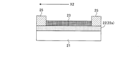
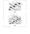
- FIG. 3 is a plan view of the probe 12.
- FIG. 3A shows the entire probe 12.
- FIG. 3B shows an enlarged view of the tip portion of the probe 12 shown in FIG. 3A.
- the portion of the probe 12 region X1 (head of the probe 12) shown in FIG. 3A is housed in the main body 11.
- the tip portion of the probe 12 projects from the main body 11.
- the tip portion of the probe 12 is inserted into the living body 2.
- the arrow X2 shown in FIG. 3A indicates the direction in which the probe 12 is inserted into the living body 2.
- the probe 12 has a substrate 21, an electrode 22, a reagent layer 23, a reference layer 24, and a film 25.
- the manufacturing method of the probe 12 will be outlined.
- the electrode 22 is formed on the substrate 21.
- the substrate 21 is, for example, a sheet-shaped synthetic resin.
- the electrodes 22 are uniformly formed on the substrate 21.
- the material of the electrode 22 is, for example, gold (Au).
- the electrode 22 may be formed on the substrate 21 by, for example, sputtering.
- the electrode 22 may be referred to as an electrode film or an electrode layer.
- the electrode 22 is separated into three regions. Grooves A1 and A2 are formed in the electrodes 22 formed on the substrate 21, and the electrodes 22 are separated into three regions.
- the electrode 22 is separated into an working electrode 22a, a reference electrode 22b, and a counter electrode 22c by grooves A1 and A2.
- the grooves A1 and A2 may be formed by, for example, laser trimming.
- the working pole 22a may be referred to as a working pole membrane or working pole layer.
- the reference electrode 22b may be referred to as a reference electrode membrane or a reference electrode layer.
- the counter electrode 22c may be referred to as a counter electrode membrane or a counter electrode layer.
- the working electrode 22a has a potential (reference electrode) sufficient to oxidize, for example, a mediator (including hydrogen peroxide as well as an electronic mediator) reduced by a reaction of an analysis (glucose) with an oxidoreductase.
- a potential reference electrode
- Glucose concentration is measured by monitoring the current flowing between the working electrode 22a and the counter electrode 22c.
- the reference layer 24 is formed.
- a reference layer 24 is formed on the reference electrode 22b at the tip of the probe 12.
- the material of the reference layer 24 is, for example, silver / silver chloride (Ag / AgCl).
- the reference layer 24 may be formed by a screen printing method or an inkjet method using, for example, Ag / AgCl paste (ink).
- the reference layer 24 may be referred to as a reference membrane or a reference electrode.
- the film 25 is arranged and fixed.
- a film 25 having an opening is arranged on the working electrode 22a, the reference electrode 22b, the counter electrode 22c, and the reference layer 24 formed on the substrate 21.
- the film 25 is in the form of a sheet and has an insulating property.
- the film 25 is arranged so that the opening portion is located at the tip portion (the portion forming the reagent layer 23) of the probe 12. A reagent described later is dropped into the opening of the film 25.
- the film 25 may be referred to as a film layer, an insulating layer, or an insulating film. Arrangement may be paraphrased as stacking or placement.
- the film 25 has an opening so that the upper surface of the counter electrode 22c (the surface in the front side direction of the paper surface in FIG. 3) is partially exposed.
- the opening of the film 25 has a notch shape as shown in the region X3 of FIG. 3 (B) by the cutting step of (7) described later. Due to this notch shape, the counter electrode 22c is partially exposed on the upper surface.
- the upper surface may be regarded as the surface on the side where the reagent layer 23 of the probe 12 is formed.
- the film 25 has a shape in which the head portion of the probe 12 is partially exposed.
- the portion of region X4 in FIG. 3A is not covered by the film 25.
- the exposed electrode 22 in the region X4 is connected to the circuit of the main body 11.
- the upper surface of the reference layer 24 is covered with the film 25 as shown in FIG. 3B.
- the reference layer 24 is exposed in the width direction of the probe 12 (perpendicular to the insertion direction indicated by the arrow X2).
- the reference layer 24 is exposed on the right side surface of the tip portion of the probe 12 (see also the reference layer 24 of FIG. 4B).
- the reagent layer 23 is formed.
- a reagent layer 23 is formed on the working electrode 22a at the tip of the probe 12.
- the reagent is dropped into the opening of the film 25 described above and dried to form the reagent layer 23.
- the reagent layer 23 is not formed at the tip of the probe 12 shown by the arrow X5 in FIG. 3 (B).
- the reagent layer 23 is preferably formed away from the tip of the probe 12. That is, it is preferable that the reagent layer 23 is not formed over a predetermined distance from the tip of the probe 12. This is because by forming the reagent layer 23 away from the tip of the probe 12, it is possible to prevent the reagent layer 23 from peeling off (turning over) from the probe 12 when the probe 12 is inserted into the living body 2.
- the reagent layer 23 contains at least an oxidoreductase capable of a redox reaction with analite (glucose).
- the reagent layer 23 may be referred to as a reagent membrane, a working layer, or a working electrode.
- the opening of the film 25 may have, for example, a size and a shape in which a reagent layer 23 having a width larger than the width of the probe 12 is formed.
- the shape of the reagent layer 23 formed to be larger than the width of the probe 12 is shaped by the next trimming step.
- the reagent layer 23 and the electrode 22 are removed.
- the reagent layer 23 and the electrode 22 are trimmed along the insertion direction of the probe 12 at the end portion in the width direction of the probe 12 whose outer shape is formed by the cutting step (7) described later.
- the upper surface of the substrate 21 is partially exposed as shown in the region X6 of FIG. 3 (B).
- laser trimming may be used for trimming the reagent layer 23 and the electrode 22.
- the film 25 is also partially (slightly) trimmed at both ends in the insertion direction of the reagent layer 23.
- the probe 12 is cut out from the substrate 21 by cutting.
- the substrate 21 that has undergone the steps (1) to (6) above is cut, and the probe 12 having the shape shown in FIG. 3 (A) is cut out.
- the cutting position includes the trimmed part. For example, the vicinity of the center (near the center line) of the trimmed portion (bottom portion of the recess) is cut.
- the tip portion of the cut probe 12 is attached to, for example, a liquid forming a protective film to form a protective film.
- the protective film prevents or suppresses leakage of substances (mainly oxidoreductases and electron mediators) contained in the reagent layer 23 to the outside of the protective film.
- the protective film has pores through which the analite existing outside the protective film permeates into the protective film in which the reagent layer 23 is present.
- the protective film only needs to be able to protect (coat) at least the portion of the reagent layer 23 of the probe 12.
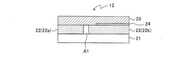
- FIG. 4A is a cross-sectional view taken along the line AA of FIG. As shown in FIG. 4A, in the portion of the probe 12 where the reagent layer 23 is formed, the working electrode 22a is formed on the substrate 21 (upper surface). The reagent layer 23 is formed on the working electrode 22a.
- the reagent layer 23 and the working electrode 22a are removed at both ends in the width direction (side surface of the probe 12) of the probe 12 by the trimming step of (6) above.
- the cutting step of (7) above the substrate 21 exposed by the trimming step of (6) above is cut at a position away from the reagent layer 23 and the working electrode 22a.
- the side surface of the probe 12 becomes stepped as shown by arrows 11a and 11b in FIG. 4A.
- a protective film is formed around the tip of the reagent layer 23 of the probe 12. In FIG. 4A, the protective film is not shown.
- FIG. 4B is a cross-sectional view taken along the line BB of FIG. As shown in FIG. 4B, in the portion where the reference layer 24 of the probe 12 is formed, the working electrode 22a and the reference electrode 22b are formed on the substrate 21. The working pole 22a and the reference pole 22b are physically and electrically separated by the groove A1.
- the reference layer 24 is formed on the reference pole 22b.
- the film 25 is arranged on the working electrode 22a, the reference electrode 22b, and the reference layer 24.
- the upper surface of the reference layer 24 is covered with the film 25, but is exposed on the side surface of the probe 12 (the right side surface in FIG. 4B).
- the film 25 above the reference layer 24 may be omitted. That is, the upper surface of the reference layer 24 may be exposed.
- FIG. 4C is a cross-sectional view taken along the line CC of FIG. As shown in FIG. 4C, in the portion where the upper surface of the counter electrode 22c is exposed, the working electrode 22a, the reference electrode 22b, and the counter electrode 22c are formed on the substrate 21.
- the working pole 22a and the reference pole 22b are physically and electrically separated by the groove A1.
- the reference electrode 22b and the counter electrode 22c are physically and electrically separated by the groove A2.
- a film 25 is formed on the working electrode 22a and the reference electrode 22b.
- the film 25 is not arranged on the counter electrode 22c, and the upper surface of the counter electrode 22c is exposed.
- the substrate 21 is a synthetic resin on a sheet.
- PET polyethylene terephthalate
- it is not particularly limited as long as it is a resin material such as a plastic material having at least one of the characteristics of flexibility, easy workability, and heat resistance.
- Other examples include general purpose plastics such as polyethylene, polypropylene, and polyethylene naphthalate.
- polyimide is preferable.
- Electrode 22 As described above, gold may be used as the material of the electrode 22. However, it is not particularly limited as long as it is a metal having conductivity and stability (for example, hard to oxidize or salt resistance) or a carbon material.
- examples of the material of the electrode 22 include platinum, palladium, and carbon.
- the metal material may be vapor-deposited (including sputtering) on the substrate 21.
- Other forming methods include printing, plating, spin coating and the like.
- carbon paste may be printed to form the electrode 22.
- different electrode materials may be used for the working electrode and the counter electrode.
- the reagent layer 23 contains at least an oxidoreductase capable of a redox reaction with analite. If the redox enzyme is a dehydrogenase, an electron mediator is further included. Further, the redox enzyme may be an oxidase (oxidase) or a system using an electron mediator. That is, if it is a system that electrochemically detects hydrogen peroxide generated by the redox reaction of glucose by an oxidase, an electron mediator is unnecessary, but it can also be detected electrochemically by using an electron mediator. In this case, the reagent layer 23 contains an electron mediator in addition to the oxidase.
- examples of redox enzymes include glucose oxidase and glucose dehydrogenase.
- glucose dehydrogenase flavin adenine dinucleotide (FAD) -linked glucose dehydrogenase is desirable from the viewpoint of low reactivity to maltose, and for example, enzymes derived from Aspergillus (Orize and Teres) and Mucor are preferable.
- FAD flavin adenine dinucleotide
- Examples of the electronic mediator include osmium complex, ruthenium complex, quinone compound, phenazine compound, ferrocene compound and the like. In addition, examples of the electronic mediator include derivatives of these.
- silver / silver chloride As the material of the reference layer 24, silver / silver chloride (Ag / AgCl) may be used as described above.
- the reference layer 24 may be formed by screen-printing or applying Ag / AgCl paste (ink) on the electrode 22 and then drying it.
- Ag / AgCl paste As another forming method, silver (Ag) may be printed, coated, plated or the like on the electrode 22, and then the surface may be chlorinated to form the electrode 22.
- the senor 1 shows an example of a three-electrode configuration of an working electrode, a counter electrode, and a reference electrode that realizes more accurate measurement, even if it is a two-electrode configuration of the working electrode and the counter electrode. good.
- ⁇ Film 25 As the film 25, a sheet made of the same material as the substrate 21 to which an adhesive sheet (for example, acrylic type, rubber type, or hot melt type) is attached may be used. Further, a sheet made of a material different from that of the substrate 21 may be used. Further, the adhesive sheet alone may be used as the film 25. A thermal / thermoplastic resist film may be used as the film 25.
- an adhesive sheet for example, acrylic type, rubber type, or hot melt type
- the contact angle with the liquid on the film is preferably higher than the contact angle with the liquid at the opening, and the larger the difference, the more preferable.
- the temperature on the film is 90 ° or more and the opening is 50 ° or less. Even if the material does not have such a contact angle, it is possible to have the contact angle by applying at least one of a water-repellent treatment to the film surface and a hydrophilic treatment to the opening.
- the film 25 has a thickness of 1 ⁇ m or more and 150 ⁇ m or less, preferably 3 ⁇ m or more and 50 ⁇ m or less, and more preferably 5 ⁇ m or more and 30 ⁇ m or less.
- the film 25 may be formed by printing a resist ink.
- the protective film covering the surface of the reagent layer 23 has biocompatibility in which proteins and cells are not adsorbed or proteins and cells are not easily adsorbed.
- the protective film is preferably formed of a polymer having the above-mentioned properties.
- polymer examples include a copolymer of methyl methacrylate and hydroxyethyl methacrylate, a copolymer of butyl methacrylate and hydroxyethyl methacrylate, poly (2-methacryloyloxyethyl phosphorylcholine-con-butyl methacrylate) and the like.
- high molecular weight polymer examples include (meth) acrylate compounds having the same main chain as these exemplified polymers and having a reactive group capable of reacting with the linker in the side chain. It can also be used as an "ethylene-based polymer" having a methacryloyl group or an acryloyl group.
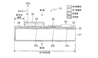
- FIG. 5 is a diagram for explaining the positional relationship between the reagent layer 23 and the film 25.
- FIG. 5 shows a plan view of the tip portion of the probe 12.
- the same components as those in FIG. 3 are designated by the same reference numerals.
- FIG. 5 shows a part of the manufacturing process of the probe 12.
- the “film formation” shown in FIG. 5 corresponds to the step (4) described above.
- “Applying the reagent solution” and “drying the applied reagent solution” correspond to the step (5) described above.
- “Trimming” corresponds to the step (6) described above.
- “Sensor cutting” corresponds to the step (7) described above.
- the “protective film formation” corresponds to the step (8) described above.
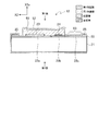
- FIG. 6 is a cross-sectional view taken along the line DD of FIG.
- a film 25 having an opening is arranged on the working electrode 22a. Then, the reagent is dropped onto the opening portion of the film 25 and dried. As a result, the reagent layer 23 is sandwiched and formed between the films 25 in the insertion direction of the probe 12, as shown in FIG. That is, the reagent layer 23 fits and is formed in the region defined by the opening of the film 25. In other words, the film 25 is adjacent to the reagent layer 23 on the electrode 22.
- the film 25 on the insertion direction side does not have to be formed.
- the film 25 on the left side shown in FIGS. 5 and 6 may be omitted.
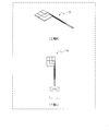
- FIG. 7 is a perspective view of the reagent layer 23 portion of the probe 12.
- the probe 12 faces the upper surface 31 on which the reagent layer 23 is formed, the back surface 32 facing the upper surface 31, the side surface 33 connecting the upper surface 31 and the back surface 32, and the side surface 33. It has a side surface 34 that connects the upper surface 31 and the back surface 32.
- the arrow X2 shown in FIG. 7 indicates the insertion direction of the probe 12 into the living body 2.
- the end of the upper surface 31 in the width direction of the probe 12 has stepped trimming portions 35 and 36 from which the reagent layer 23 and the electrode 22 have been removed.
- the trimming portions 35 and 36 are formed at least in a positional relationship in contact with the reagent layer 23.
- the reagent layer 23 extends from end to end in the width direction of the upper surface 31 to form the upper surface 31 of the probe 12 and forms a part of the side surface of the probe 12 (reagent layer of FIG. 4A). See also 23).
- the above sensor 1 may be regarded as having the following components.
- the sensor 1 has a main body 11 and a probe 12.
- the probe 12 is inserted into the living body 2 and acquires an electric signal for continuously or semi-continuously measuring the analyst.
- the substrate 21 has a first surface (for example, an upper surface 31) and a second surface (for example, a back surface 32) facing the first surface. Further, the substrate 21 has a third surface and a fourth surface (for example, side surfaces 33 and 34) of a surface that connects the first surface and the second surface and extends in the insertion direction of the probe 12.
- the working electrode 22a is formed on the first surface of the substrate 21 in the first electrode material.
- the reagent layer 23 is arranged in a part of the working electrode 22a.
- the trimming portions 35 and 36 are formed by removing the reagent layer 23 and the first electrode material at both ends of the first surface in a direction orthogonal to the direction in which the probe 12 is inserted into the living body 2. ..
- the reagent layer 23 contains an oxidoreductase.
- the trimming portions 35 and 36 are formed in a positional relationship of at least in contact with the reagent layer 23.
- the film 25 is adjacent to the reagent layer 23 in the direction of insertion into the living body 2 in the direction opposite to the tip end side of the probe 12.
- the reagent layer 23 does not have a portion sandwiched between the electrode 22 and the film 25.
- the film 25 is not placed on the reagent layer 23.
- the film 25 may or may not be adjacent to the reagent layer 23 on the distal end side of the probe 12. In other words, the film 25 may or may not be formed on the distal end side of the probe 12.
- the above sensor 1 may be regarded as having the following manufacturing process.
- a substrate 21 (substrate sheet) in which the working electrode 22a of the first electrode material is formed on the first surface is prepared.
- the reagent solution is dried to form the reagent layer 23.
- a predetermined position of the reagent layer 23 on the substrate 21 is trimmed to form a trimming portion from which the working electrode 22a formed under the reagent layer 23 and the reagent layer 23 has been removed.
- the substrate 21 is cut into a predetermined shape (the shape of the probe 12 shown in FIG. 3A, for example, the shape of a flagpole).
- the trimming portions 35 and 36 are included in the positions where the substrate 21 is cut.
- a protective film may be formed at the tip of the probe 12 on which the reagent layer 23 is formed.
- the protective film has pores that allow at least an analysis (glucose) to pass through.
- the counter electrode 22c may be formed on the first surface of the substrate 21 or may be formed on the second surface.
- Another counter electrode (second counter electrode) different from the counter electrode 22c may be formed on both or one of the first surface and the second surface of the substrate 21.
- the reference electrode 22b may be formed on at least one of the first to fourth surfaces.
- the film 25 may be arranged on the upper surface and the third surface side may be exposed.
- the reagent layer 23 does not have to be formed over a predetermined distance from the terminal side (tip of the probe 12) of the first surface in the insertion direction of the probe 12.
- a part (end) of the reagent layer 23 may be sandwiched between the electrode 22 and the film 25.
- the reagent layer 23 does not have to have a portion sandwiched between the electrode 22 and the film 25.
- the sensor 1 has a probe 12 inserted into the living body 2 and measures the analyst.
- the probe 12 has a substrate 21, an electrode 22 formed on the substrate 21, and a reagent layer 23 containing an oxidoreductase and formed on the electrode 22.
- the reagent layer 23 and the electrode 22 are trimmed along the insertion direction of the probe 12 into the living body 2.
- the variation in performance of the sensor 1 caused by the manufacturing process is suppressed.
- a uniform (uniform) portion in the ring is used as the reagent layer 23 by trimming. Available.
- the cutting edge when cutting into the probe 12 shape, the cutting edge can be prevented from coming into contact with the reagent layer 23, and cracking of the reagent layer 23 can be reduced.
- the cutting edge when cutting into the probe 12 shape, the cutting edge can be prevented from coming into contact with the reagent layer 23, and contamination of the reagent can be suppressed.
- the probe 12 included in the sensor 1 has a step of forming the electrode 22 on the substrate 21, a step of forming the reagent layer 23 containing the oxidoreductase on the electrode 22, and the width of the probe 12.
- Manufactured by a step of trimming the reagent layer 23 and the electrode 22 along the insertion direction of the probe 12 into the living body 2 at at least one end in the direction.
- the variation in performance of the sensor 1 caused by the manufacturing process is suppressed.
- a uniform (uniform) central portion in the ring can be used as the reagent layer 23 by trimming.
- the cutting edge when cutting into the shape of the probe 12, the cutting edge can be prevented from coming into contact with the reagent layer 23 by trimming, so that cracking of the reagent layer 23 can be reduced. In addition, contamination of reagents can be suppressed.
- the film 25 is arranged on the electrode 22 so as to be adjacent to the reagent layer 23 at both ends in the insertion direction of the reagent layer 23.
- the film 25 can determine the position where the reagent is dropped, and a uniform reagent layer 23 can be formed before trimming.
- the probe 12 may have a trimming section at one end in the width direction. That is, the number of trimming portions may be one.
- FIG. 8 is a plan view of the tip portion of the probe 12.
- the same components as those in FIG. 3 are designated by the same reference numerals.
- FIG. 8 shows an example in which the working electrode 22a and the counter electrode 22c are formed side by side in the width direction of the probe 12. In FIG. 8, the film 25 is not shown.
- the reagent layer 23 is formed so as to straddle the width of the probe 12 on one end side in the width direction of the probe 12.
- the reagent layer 23 is formed on the other end side in the width direction of the probe 12 so as not to straddle the width of the probe 12.
- the reagent layer 23 is formed so as to straddle the right end of the probe 12 and not to straddle the left end of the probe 12.
- the probe 12 has a trimming portion 41.
- the trimming portion 41 is formed on the side where the reagent layer 23 straddles the width of the probe (on the right side in FIG. 6).
- the trimming portion 41 is formed by trimming the reagent layer 23 and the working electrode 22a.
- the trimming section 41 exposes the substrate 21.
- the probe 12 may have a trimming portion at one end in the width direction. This also suppresses the variation in performance of the sensor 1 caused by the manufacturing process.
- the reagent layer 23 may protrude outside the region defined by the film 25 in the insertion direction of the probe 12.
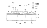
- FIG. 9 is a diagram for explaining the positional relationship between the reagent layer 23 and the film 25.
- FIG. 9 shows a plan view of the tip portion of the probe 12.
- the same components as those in FIG. 3 are designated by the same reference numerals.
- FIG. 9 shows a part of the manufacturing process of the probe 12.
- “Applying the reagent solution” and “drying the applied reagent solution” shown in FIG. 9 correspond to the step (5) described above.
- the “film formation” corresponds to the step (4) described above.
- “Trimming” corresponds to the step (6) described above.
- “Sensor cutting” corresponds to the step (7) described above.
- the “protective film formation” corresponds to the step (8) described above.
- FIG. 10 is a cross-sectional view taken along the line EE of FIG.
- a film 25 having an opening is arranged on the reagent layer 23.
- the film 25 is arranged so that the opening portion is located in the reagent layer 23.
- the openings of the film 25 are formed so as to overlap the reagent layer 23 at both ends of the reagent layer 23 in the insertion direction (direction of arrow X2). That is, a part of the film 25 overlaps the reagent layer 23 at both ends of the reagent layer 23 in the insertion direction. Further, a part of the film 25 overlaps the trimming portion at both ends in the insertion direction of the trimming portion.
- the film 25 on the insertion direction side does not have to be formed.
- the film 25 on the left side shown in FIGS. 9 and 10 may be omitted.
- the film 25 is arranged on the electrode 22 so as to overlap the reagent layer 23 and the trimming portion at both ends of the reagent layer 23 in the insertion direction.
- the variation in performance of the sensor 1 caused by the manufacturing process is suppressed.
- the end portion (edge portion of the coffee ring) of the reagent layer 23 in the insertion direction of the probe 12 can be covered with the film 25 to expose a uniform portion of the reagent layer 23.
- FIG. 11 is a diagram showing an example of the opening shape of the film 25.
- the hatched portions of FIGS. 11A and 11B indicate trimming portions.
- the figures such as the polygonal shape and the round shape shown in (A) of FIG. 11 and (B) of FIG. 11 indicate the shape of the opening portion of the film 25.
- the arrow X2 shown in FIG. 11 indicates the direction in which the probe 12 is inserted into the living body 2.
- films 25 are formed at both ends of the reagent layer 23 in the insertion direction (see, for example, FIGS. 5 and 6).
- a film 25 is formed at the end of the reagent layer 23 opposite to the tip end side (for example, the film 25 on the right side of FIGS. 5 and 6 is formed, and the film 25 on the left side is formed. Not done).
- the opening shape of the film 25 may have various shapes.
- FIG. 12 is a diagram illustrating an example of the size of the sensor 1.
- the same components as those in FIGS. 3 and 7 are designated by the same reference numerals.
- the film 25 is not shown.
- the width D1 of the tip portion of the probe 12 is, for example, 70 ⁇ m or more and 1700 ⁇ m or less.
- the width D1 is 70 ⁇ m or more and 600 ⁇ m or less, more preferably 70 ⁇ m or more and 400 ⁇ m or less.
- the width D2 of the trimming portions 35 and 36 is, for example, 5 ⁇ m or more.
- the width D2 is not particularly limited as long as it has a width that can secure the reagent layer 23 with respect to the width of the tip portion of the probe 12.
- it can be realized by irradiating the laser a plurality of times.
- the protective film covering the outer periphery of the probe will be described.
- the protective film may be referred to as a bioprotective film.
- the protective film has pores sized to allow small molecule compounds to pass through.
- the protective membrane has pores sized to allow glucose as an analyst to permeate. As a result, glucose in the outside of the probe can permeate the protective membrane and reach the probe.
- a sensor such as a CGM sensor embedded in a living body prevents a reagent in a reagent layer formed on the probe from leaking into the living body while measuring a glucose concentration or the like by a protective film.
- the protective film may be formed (coated) at least on a portion covering the reagent layer. Therefore, the protective film may be formed by a dip method.
- the protective film component is dissolved in an organic solvent such as ethanol, and the probe is immersed in the protective film solution.
- an organic solvent such as ethanol
- the formation of the protective film by the dip method is complicated in the manufacturing process.
- the thickness and shape of the protective film vary from sensor to sensor, resulting in variations in performance.
- the variation of the protective film can be suppressed, but the number of times of immersion and drying increases, which complicates the manufacturing process.
- a protective film solution having a high concentration of protective film components is used to simplify the manufacturing process and the number of times of immersion and drying is reduced, the thickness and shape of the protective film vary, and the performance varies.
- FIG. 13 is a perspective view of the probe 12 of the sensor 1 according to the second embodiment.
- the same components as those in FIGS. 2 and 3 are designated by the same reference numerals.
- the probe 12 shown in FIG. 13 has an electrode 22 like the probe 12 described in the first embodiment. Further, the probe 12 includes a reagent layer 23 (not shown in FIG. 13) and a reference layer 24 (not shown in FIG. 13), similarly to the probe 12 described in the first embodiment. The first surface has a counter electrode 22c (not shown in FIG. 13), which is partially exposed.
- the surface of the probe 12 on which the reagent layer 23 and the reference layer 24 are formed may be referred to as a first surface.
- the surface facing the first surface may be referred to as a second surface.
- the direction from the second surface to the first surface (direction of arrow X2a in FIG. 13) may be referred to as a height direction.
- a surface that connects the first surface and the second surface and extends in the insertion direction of the probe 12 (direction of arrow X2 in FIG. 13), and the surface on the right side when viewed from the tip of the probe 12 is the third surface. May be called.
- a surface that connects the first surface and the second surface and extends in the insertion direction of the probe 12, and the surface on the left side when viewed from the tip of the probe 12 may be referred to as a fourth surface.
- the surface of the probe 12 facing the insertion direction may be referred to as a tip surface.
- the first surface may be referred to as the upper surface.
- the second surface may be referred to as the bottom surface.
- the third and fourth surfaces may be referred to as side surfaces.
- FIG. 14 is a partial side view of the probe 12 of FIG. 13 as viewed from the third surface side.
- FIG. 14 shows the probe 12 before the protective film described later is formed.
- an electrode 22 is formed on the first surface side of the substrate 21.
- the electrode 22 has an working electrode 22a, a reference electrode 22b, and a counter electrode 22c.
- a reagent layer 23 is formed on the first surface side of the working electrode 22a of the electrode 22.
- a reference layer 24 is formed on the first surface side of the reference electrode 22b of the electrode 22.
- the reference layer 24 is formed by curing the Ag / AgCl paste applied on the reference electrode 22b.
- the working electrode 22a at the tip of the probe 12 (the working pole 22a on the tip side of the probe 12 with the reagent layer 23 as a boundary) is covered with the film 25.
- the film 25 covering the working electrode 22a at the tip of the probe 12 was in contact with the reagent layer 23, but may be separated as shown by the arrow A21 in FIG.
- the film 25 has an opening in the portion corresponding to the reagent layer 23. As a result, the first surface side of the reagent layer 23 is exposed.
- the first surface side of the reference layer 24 is covered with the film 25. In other words, the first surface side of the reference layer 24 is not exposed.
- the reference layer 24 is exposed on the third surface side of the probe 12. In other words, the reference layer 24 is exposed in the width direction of the probe 12 (perpendicular to the insertion direction indicated by the arrow X2) (see also FIG. 4B).
- the film 25 has an opening so that the portion in the region X3 on the first surface side of the counter electrode 22c is exposed.
- the opening of the film 25 has a notch shape (see also region X3 in FIG. 3B). Due to this notch shape, the counter electrode 22c is partially exposed on the upper surface.
- the portion of the working pole 22a from the head of the probe 12 (the portion of the region X1 in FIG. 13) to the reagent layer 23 may be referred to as a lead or a working pole lead.
- the portion of the reference electrode 22b from the head of the probe 12 to the reference layer 24 may be referred to as a lead or a reference electrode lead.
- the portion of the counter electrode 22c from the head of the probe 12 to the opening (region X3) of the film 25 may be referred to as a lead or counter electrode lead.
- the reference layer 24 may be exposed on the fourth surface side. Further, the reference layer 24 and the counter electrode 22c may be formed on the second surface side. When the reference layer 24 and the counter electrode 22c are formed on the second surface side, the reference electrode lead and the counter electrode lead are formed on the second surface side.
- FIG. 15 is a partial side view of the probe 12 on which the protective film is formed as viewed from the third surface side.
- a first protective film 51 and a second protective film 52 are formed on the probe 12 of FIG.
- the first protective film 51 and the second protective film 52 may be simply referred to as a protective film.
- the first protective film 51 is formed so as to cover the reagent layer 23 formed on the working electrode 22a.
- the first protective film 51 is formed so as to cover the first surface side, the third surface side, the fourth surface side, the tip surface side, and the surface side opposite to the tip surface side of the reagent layer 23. ..
- the second protective film 52 covers the electrode 22, the reagent layer 23, the reference layer 24, and the film 25 formed on the substrate 21 (for example, so as to cover the tip portion of the probe 12 shown in FIG. 14). )It is formed.
- the second protective film 52 includes a film 25 arranged at least on the working electrode 22a from the tip of the probe 12, a reagent layer 23 and a first protective film 51 formed on the working electrode 22a, and a reference electrode 22b. It is formed so as to cover the reference layer 24 and the film 25 arranged above and the film 25 having an opening arranged on the counter electrode 22c.
- the second protective film 52 is formed so as to cover a portion from the tip of the probe 12 to a first predetermined distance exceeding at least the region X3.
- the second protective film 52 may be formed on the first surface side, the second surface side, the third surface side, the fourth surface side, and the tip surface side of the probe 12.
- the reagent layer 23 is formed at a position separated from the end of the probe 12 in the insertion direction into the living body by a predetermined distance. For example, as shown in FIG. 15, the reagent layer 23 is formed from a position separated from the tip of the probe 12 by a second distance.
- the counter electrode 22c exposed from the opening (region X3) of the reference layer 24 and the film 25 is formed in a region opposite to the tip end side of the probe 12 with the reagent layer 23 as a boundary.
- the first protective film 51 is formed by a sensor manufacturing method described later.
- the first protective film 51 is formed by arranging a film formed of the protective film material so as to cover the reagent layer 23.
- the first protective film 51 is not arranged from the tip of the probe 12 to the second predetermined distance. This is to make the tip of the probe 12 as thin as possible in consideration of the ease of insertion of the probe 12 into the living body. Further, if the first protective film 51 (including the reagent layer 23) is arranged at the tip of the probe 12, there is a possibility that the first protective film 51 (including the reagent layer 23) may dissociate when inserted into a living body.
- the first protective film 51 is thicker than the second protective film.
- the thickness of the first protective film 51 (the thickness of the first protective film 51 does not include the thickness of the second protective film 52 arranged on the first protective film 51) is determined in the height direction of the probe 12. It is thicker than the thickness of the second protective film arranged on the second predetermined distance on the first surface.
- the first protective film 51 and the second protective film 52 allow the analytes existing outside the protective film to permeate into the protective film, while the outer protective film of the substance (mainly oxidoreductase) contained in the reagent layer 23. Since it is necessary to prevent or suppress leakage to, these protective membranes need only have pores of a size that allows sufficient permeation of analite and impermeability or difficulty of permeation of oxidoreductase, and are the same material. It may be a different material.
- the first protective film 51 may be coated with the working electrode 22a including the reagent layer 23 as shown in FIG. 15, or may also be coated with the reference layer 24 as shown in FIG.
- FIG. 16 is a partial side view of the probe 12 on which the protective film is formed as viewed from the third surface side.
- the same components as in FIG. 15 are designated by the same reference numerals.
- the first protective film 51 may also cover the reference layer 24.
- the film 25 may not be arranged on the upper surface of the reference layer 24.
- the first protective film 51 may also cover the counter electrode 22c (counter electrode 22c of the region X3 portion) exposed from the film 25.
- the reference electrode 22b or the counter electrode 22c is arranged on the same surface as the working electrode 22a.
- 17A-17D are diagrams illustrating an example of a method for manufacturing the probe 12.
- step A a protective film sheet that serves as a base for the first protective film 51 is formed.
- the protective film sheet may be referred to as a protective film film.
- tBuMA4VP which is a protective film material
- PEGDGE poly (ethylene glucol) diglycidyl ether
- the protective film solution 61 is uniformly spread on the base material sheet 62 using the squeegee 63, and then dried. That is, a protective film as a base of the first protective film 51 is formed on the base sheet 62.
- the thickness of the protective film formed on the base sheet may be, for example, 20 ⁇ m. If the predetermined thickness is not reached by spreading the coating once, the coating may be repeated a plurality of times.
- the base material sheet After forming a protective film having a predetermined thickness, the base material sheet is cut into a shape having substantially the same diameter as the opening diameter (for example, ⁇ 3.5 mm) of step H described later.
- the thickness of the protective film formed on the base sheet may be in the range of 5 ⁇ m or more and 60 ⁇ m or less. It is more preferably in the range of 10 ⁇ m or more and 45 ⁇ m or less, and further preferably in the range of 20 ⁇ m or more and 40 ⁇ m or less.
- the protective film component concentration and the cross-linking agent concentration in the protective film solution are 1/4 or more and 1/2 or less by weight percent (w / v%) of the dissolution limit concentration of the protective film component with respect to the dissolving solvent.
- the dissolution limit concentration of tBuMA4VP in ethanol is about 20%, it is preferably 5 w / v% or more and 10 w / v% or less.
- the PEDGE concentration of the cross-linking agent is preferably 0.39 w / v% or more and 0.78% w / v or less because the dissolution limit in ethanol is about 1.55%.
- the organic solvent to be dissolved ethanol is used in step A and step J described later, but it can dissolve the protective film solution and gives the influence of the oxidoreductase used (causes a large decrease in enzyme activity, etc.).
- the soluble organic solvent is preferably an alcohol solvent.
- the alcohol-based solvents a lower alcohol-based solvent (carbon chain is 6 or less) is preferable, and examples other than ethanol include methanol and isopropyl alcohol. Further, these organic solvents may be used in combination of a plurality of types.
- Step B As shown in FIG. 17A (step B), the electrode 22 is formed on the substrate 21 on the sheet.
- an electrode material such as gold is sputtered onto a sheet-shaped substrate 21 such as polyethylene terephthalate (PET) to form an electrode 22.
- PET polyethylene terephthalate
- Step C As shown in (Step C) of FIG. 17A, the working electrode 22a, the reference electrode 22b, and the counter electrode 22c are formed.
- laser processing is used to form the working pole 22a, the reference pole 22b, and the counterpole 22c.
- FIG. 17A shows an example in which the working electrode 22a, the reference electrode 22b, and the counter electrode 22c are formed on one surface.
- the reference layer 24 is formed on the reference electrode 22b.
- the reference layer 24 is formed by applying Ag / AgCl paste on the reference electrode 22b and then drying it. At that time, the Ag / AgCl paste is arranged so as to straddle the reference electrode 22b and the portion outside the probe 12 (the portion separated from the probe 12).
- FIG. 17B is an enlarged view of the dotted line frame A31 portion of FIG. 17A (process C).
- step D reference poles 22b, grooves A1 and A2, and Ag / AgCl paste formed on the substrate 21 are shown.
- step D the head, tip, reagent layer 23, and film 25 of the probe 12 are not shown.
- the first film 71 (a film different from the film 25) is attached on the sheet-shaped substrate 21.
- the first film 71 has an opening in a portion where the reagent layer 23 is formed and a portion where the counter electrode 22c is exposed (for example, a portion in the region X3 shown in FIG. 14).
- the opening of the portion of the first film 71 and the film 25 where the reagent layer 23 is formed may be referred to as the first opening.
- the opening of the portion of the first film 71 and the film 25 where the counter electrode 22c is exposed may be referred to as a second opening.
- the arrow A32 in FIG. 17B (step E) indicates the first opening of the first film 71.
- the second opening of the first film 71 is not shown.
- the contact angle with the liquid on the first film 71 is preferably higher than the contact angle with the liquid at the opening, and the larger the difference, the more preferable.
- the diameter of the first opening of the first film 71 may be, for example, 2.5 mm. Further, in the first film 71, the second opening does not have to be formed.
- Step F As shown in (Step F) of FIG. 17C, the reagent solution is applied to the first opening of the first film 71 attached to the sheet-shaped substrate 21, and the reagent layer 23 is formed.
- Step G As shown in (Step G) of FIG. 17C, the reagent layer 23 and the electrode material portion (working electrode 22a) are trimmed (for trimming, refer to the first embodiment).
- the probe 12 in the second embodiment does not have to be trimmed (step G).
- Step H The first film 71 attached in step E is peeled off from the substrate 21. Then, as shown in (Step H) of FIG. 17C, the film 25 having the first opening and the second opening is attached to the sheet-shaped substrate 21. The first opening of the film 25 is located in the portion of the reagent layer 23, and the second opening is located in the portion of region X3 of the counter electrode 22c. The upper surface of the reference layer 24 is covered with the film 25. In (Step H) of FIG. 17C, the second opening of the film 25 is not shown.
- the diameter of the first opening of the film 25 is larger than the diameter of the first opening of the first film 71, and may be, for example, 3.5 mm. That is, the first opening of the film 25 may have a size surrounding the reagent layer 23.
- Step I As shown in (Step I) of FIG. 17D, ethanol 72 is applied to the first opening of the film 25.
- ethanol 72 is applied to cover the first opening.
- the diameter of the first opening is 3.5 mm
- ethanol 72 of about 3 ul or more and 5 ul or less is applied.
- the film 25 is formed by the contact angle formed by the liquid (in this case, ethanol 72) and the film 25 in contact with the film 25, and the liquid in the first opening (in this case, ethanol 72).
- the material of the film 25 such that the contact angle of the former is larger. This is because the applied liquid (in this case, ethanol 72) is kept in the first opening so that the liquid does not leak from the first opening.
- the larger the difference in contact angle between the two the more preferable.
- the difference between the contact angles of the two is, for example, preferably 20 ° or more, more preferably 35 ° or more, and further preferably 50 ° or more.
- step J As shown in (step J) of FIG. 17D, the protective film sheet 73 formed and cut in step A is arranged (placed) in the first opening of the film 25 as shown by arrow A33. Then, the ethanol 72 applied in step I is dried. As a result, the protective film sheet 73 is partially dissolved by ethanol 72 and dried, so that the first protective film 51 in close contact with the reagent layer 23 can be formed.
- Step K As shown in (Step K) of FIG. 17E, the sheet-shaped substrate 21 is cut so as to have the shape of the probe 12.
- Step L As shown in (Step L) of FIG. 17E, the cut probe 12 is dipped in a protective film solution (which may have a different composition) having the same composition as that of Step A and dried. The dipping and drying may be repeated, for example, at any number of times 1 or more and 3 or less. As a result, the second protective film 52 is formed on the probe 12.
- a protective film solution which may have a different composition
- the thickness of the second protective film 52 is preferably in the range of 5% or more and 60% or less of the thickness of the first protective film 51.
- the thickness of the second protective film 52 is more preferably in the range of 10% or more and 50% or less, and further preferably in the range of 20% or more and 40% or less.
- one dip is 1 ⁇ m or more and 4 ⁇ m or less, two dips are 2 ⁇ m or more and 8 ⁇ m or less, and three dips are 3 ⁇ m or more.
- a second protective film 52 having a thickness of 12 ⁇ m or less can be formed.
- Coating method 2a Structure of probe 12
- the probe 12 manufactured by the coating method has basically the same structure as the probe 12 manufactured by the film pasting method. The differences in configuration will be described below.
- FIG. 18 is a partial side view of the probe 12 on which the protective film is formed as viewed from the third surface side.
- FIG. 19 is a top view of the tip portion of the probe 12 of FIG.
- the shape of the first protective film 51 is different from the shape of the first protective film 51 (for example, see FIG. 15) formed by the film pasting method.
- both ends of the first protective film 51 formed by the coating method rise in the direction along the insertion direction of the probe 12 into the living body.
- the first protective film 51 has a convex shape at both ends in the direction in which the probe 12 is inserted into the living body.
- the raised portion of the first protective film 51 may be referred to as an outer edge portion.
- the width of the outer edge portion has a third predetermined distance as shown in FIG.
- the region sandwiched between the outer edges of the first protective film 51 may be referred to as the inside.
- the protective film solution is dropped onto the reagent layer 23 and dried to form the first protective film 51.
- the protective film solution dries, a coffee ring is formed on the outer edge portion, so that the outer edge portion (raised portion) is formed on the first protective film 51.
- the outer edge portion corresponds to a coffee ring, and the inside can be regarded as a portion other than the coffee ring.
- the outer edge portion in the direction along the insertion direction of the probe 12 is separated (removed) from the probe 12.
- the first protective film 51 is formed in a circular shape, for example, on the working electrode 22a that is not separated from the probe 12 (in other words, on the working electrode 22a that remains on the probe 12 after cutting).
- a circular coffee ring (outer edge) is formed. That is, the outer edge portion of the first protective film 51 is included at least at both ends in the insertion direction of the probe 12 into the living body.
- the first protective film 51 may be coated with the working electrode 22a including the reagent layer 23 as shown in FIG. 18, or may also be coated with the reference layer 24 as shown in FIG. 20.
- FIG. 20 is a partial side view of the probe 12 on which the protective film is formed as viewed from the third surface side.
- the same components as in FIG. 18 are designated by the same reference numerals.
- the first protective film 51 may also cover the reference layer 24.
- the film 25 may not be arranged on the upper surface of the reference layer 24.
- the first protective film 51 may also cover the counter electrode 22c (counter electrode 22c of the region X3 portion) exposed from the film 25.
- the reference electrode 22b or the counter electrode 22c is arranged on the same surface as the working electrode 22a.
- 21A-21D are diagrams illustrating an example of a method for manufacturing the probe 12.
- the electrode 22 is formed on the substrate 21 on the sheet.
- an electrode material such as gold is sputtered onto a sheet-shaped substrate 21 such as polyethylene terephthalate (PET) to form an electrode 22.
- PET polyethylene terephthalate
- Step B As shown in (Step B) of FIG. 21A, the working electrode 22a, the reference electrode 22b, and the counter electrode 22c are formed. For example, laser processing is used to form the working pole 22a, the reference pole 22b, and the counterpole 22c. In FIG. 21A (step B), an example is shown in which the working electrode 22a, the reference electrode 22b, and the counter electrode 22c are formed on one surface.
- the reference layer 24 is formed on the reference electrode 22b.
- the reference layer 24 is formed by applying Ag / AgCl paste on the reference electrode 22b and then drying it. At that time, the Ag / AgCl paste straddles the reference electrode 22b and the portion outside the probe 12 (the portion separated from the probe 12) when the substrate 21 is cut in the cutting process of step K described later. Deploy.
- Step D As shown in (Step D) of FIG. 21B, the first film 71 (a film different from the film 25) is attached on the sheet-shaped substrate 21.
- the first film 71 has an opening in a portion where the reagent layer 23 is formed and a portion where the counter electrode 22c is exposed (for example, a portion in the region X3 shown in FIG. 18).
- the opening of the portion of the first film 71 and the film 25 where the reagent layer 23 is formed may be referred to as the first opening.
- the opening of the portion of the first film 71 and the film 25 where the counter electrode 22c is exposed may be referred to as a second opening.
- the arrow A32 in FIG. 21B (step D) indicates the first opening.
- the second opening is not shown.
- the contact angle with the liquid on the first film 71 is preferably higher than the contact angle with the liquid at the opening, and the larger the difference, the more preferable.
- the diameter of the first opening of the first film 71 may be, for example, 2.5 mm. Further, in the first film 71, the second opening does not have to be formed.
- Step E As shown in (Step E) of FIG. 21B, the reagent solution is applied to the first opening of the first film 71 attached to the sheet-shaped substrate 21, and the reagent layer 23 is formed.
- Step F As shown in (Step F) of FIG. 21C, the reagent layer 23 and the electrode material portion (working electrode 22a) are trimmed (for trimming, refer to the first embodiment).
- the probe 12 in the second embodiment does not have to be trimmed (step F).
- Step G The first film 71 attached in step D is peeled off from the substrate 21. Then, as shown in (Step G) of FIG. 21C, the film 25 having the first opening and the second opening is attached to the sheet-shaped substrate 21. The first opening of the film 25 is located in the portion of the reagent layer 23, and the second opening is located in the portion of region X3 of the counter electrode 22c. The upper surface of the reference layer 24 is covered with the film 25.
- the diameter of the first opening of the film 25 is larger than the diameter of the first opening of the first film 71, and may be, for example, 3.2 mm. That is, the diameter of the first opening of the film 25 may have a size surrounding the reagent layer 23.
- the protective film solution 74 is applied to the first opening of the film 25.
- a protective film solution 74 that covers the first opening is applied.
- the applied protective film solution 74 is dried to form the first protective film 51.
- the film 25 includes a contact angle formed by the liquid (in this case, the protective film solution 74) and the film 25 in contact with the film 25, and the liquid in the first opening (in this case, the protective film solution 74).
- the material of the film 25 such that the contact angle of the former is larger. This is because the applied liquid (in this case, the protective film solution 74) is kept in the first opening so that the liquid does not leak from the first opening.
- the larger the difference in contact angle between the two the more preferable.
- the difference between the contact angles of the two is, for example, preferably 20 ° or more, more preferably 35 ° or more, and further preferably 50 ° or more.
- the protective membrane solution 74 is prepared by dissolving tBuMA4VP and poly (ethylene glucol) diglycidyl ether (hereinafter referred to as PEGDGE) as a cross-linking agent in ethanol so that the final concentrations are 8% and 0.62%, respectively. To create.
- the drying temperature may be, for example, in the range of 10 ° C. or higher and 65 ° C. or lower. Drying may be performed, for example, for several minutes or more and several tens of minutes or less.
- Step I As shown in (Step I) of FIG. 21D, the sheet-shaped substrate 21 is cut so as to have the shape of the probe 12.
- Step J As shown in (Step J) of FIG. 21D, the cut probe 12 is dipped in a protective film solution (which may have a different composition) having the same composition as that of Step H and dried. The dipping and drying may be repeated, for example, at any number of times 1 or more and 3 or less. As a result, the second protective film 52 is formed on the probe 12.
- a protective film solution which may have a different composition
- the thickness of the second protective film 52 is preferably in the range of 5% or more and 60% or less of the thickness of the first protective film 51.
- the thickness of the second protective film 52 is more preferably in the range of 10% or more and 50% or less, and further preferably in the range of 20% or more and 40% or less.
- one dip is 1 ⁇ m or more and 4 ⁇ m or less, two dips are 2 ⁇ m or more and 8 ⁇ m or less, and three dips are 3 ⁇ m or more.
- a second protective film 52 having a thickness of 12 ⁇ m or less can be formed.
- FIG. 22 is a diagram illustrating a shape example of the first protective film 51 formed in step H.
- FIG. 22 shows a top view of the first protective film 51 and a cross-sectional view taken along the line AA. Further, the dotted line X11 shown in FIG. 22 indicates a cut line to be cut in the step I.
- the first protective film 51 has a circular coffee ring after the step H.
- the probe 12 remains a portion of the circular coffee ring surrounded by the dotted frame X12. That is, the first protective film 51 has outer edges at both ends of the first protective film 51 in the direction of insertion of the probe 12 into the living body.
- the probe 12 of the sensor 1 inserted into the living body and measuring the analyze includes the substrate 21, the electrode 22 formed on the substrate 21, and the reagent layer 23 formed on the electrode 22. It has a first protective film 51 formed on the reagent layer 23, and a second protective film 52 formed on the first protective film 51, which is thinner than the first protective film 51.
- the senor 1 forms the first protective film 51 on the reagent layer 23, and forms the second protective film 52 thinner than the first protective film 51 on the first protective film 51, so that the reagent layer 23
- the number of steps for forming the protective film is reduced, and variations in thickness and shape are suppressed. Therefore, the sensor 1 can be easily manufactured, and variations in performance are suppressed.
- a sheet-shaped first protective film 51 having a predetermined thickness manufactured in advance is attached to a position including at least the reagent layer 23 portion of the probe 12.
- a paste-like first protective film 51 having a predetermined thickness is applied to a position of the probe 12 including at least the reagent layer 23 portion.
- the dip forming the second protective film 52 is one in which immersion and drying are repeated 1 or more and 5 or less, preferably 1 or more and 3 or less times, and the surface of the probe 12 of the first protective film 51 portion is covered. The number of times it can be covered may be sufficient.
- the senor 1 can be easily manufactured by reducing the number of steps for forming the protective film of the reagent layer 23. Further, the sensor 1 can suppress variations in the thickness and shape of the protective film by forming a second protective film 52 thinner than the first protective film 51 on the first protective film 51 formed to be thick to some extent, and variations in performance. Can be suppressed.
- a typical example is polyethylene phthalate as the substrate.
- the material is not particularly limited as long as it is a resin material or a plastic material having flexibility, easy workability, and heat resistance.
- Other examples include, for example, polyethylene, polypropylene, and polyethylene terephthalate-based general-purpose plastics.
- polyimide is preferable.
- the electrode material used for the working electrode and the counter electrode is not particularly limited as long as it is a metal or carbon material having conductivity and stability (hard to oxidize, salt resistance). Examples of such electrode materials include gold, platinum, palladium and carbon. When a metal material is used, the electrode material can be formed on the substrate by sputtering, vapor deposition, printing, plating, or spin coating.
- electrodes When carbon is used, electrodes may be formed by screen printing using carbon paste.
- the electrode materials on the first surface and the second surface may be the same or different electrode materials.
- a plurality of counter electrodes may be provided.
- both the first counter electrode (first counter electrode lead) and the second counter electrode (second counter electrode lead) may be provided on the first surface or the second surface, or the first counter electrode (first counter electrode lead) may be provided on the first surface. It may be provided on the surface and the second counter electrode (second counter electrode lead) may be provided on the second surface.
- Reference layer Ag / AgCl may be used for the reference layer.
- the insulating layer is formed of a film or resist ink. It is preferable to use a film that is basically the same material as the substrate and has an adhesive sheet (for example, acrylic type, rubber type, hot melt type) attached to the film. However, the adhesive sheet alone may be used as a film.
- a thermal / thermoplastic resist film can be mentioned.
- a general-purpose plastic film is used, and from the viewpoint of reagent application, a material having a contact angle with a liquid having a relationship of "contact angle of film surface> contact angle of film opening" is adopted.
- the film opening referred to here refers to the surface of the working electrode before dropping and forming the reagent layer, that is, the first electrode material. Even if the material does not have such a contact angle, it is possible to have the relationship of the contact angle by treating the film surface with at least one of water-repellent treatment and hydrophilic treatment on the opening. ..
- the film has a thickness selected from a range of approximately 1 ⁇ m or more and 250 ⁇ m or less, preferably 3 ⁇ m or more and 50 ⁇ m or less, and more preferably 5 ⁇ m or more and 30 ⁇ m or less.
- the insulating layer it is preferable to use a film as described in the first embodiment and the second embodiment rather than forming the insulating layer with resist ink.
- the reagent layer contains at least an oxidoreductase that undergoes a redox reaction with analite.
- the reagent layer may or may not include an electron mediator (a system for detecting generated hydrogen peroxide). May be good.
- an electron mediator is included in the reagent layer.
- bioprotective film The bioprotective membrane prevents or suppresses the leakage of substances (mainly oxidoreductases) contained in the reagent layer to the outside of the protective membrane, and the reagent layer contains analysts existing outside the protective membrane. It has a permeable hole in the protective film. Therefore, the bioprotective film is not particularly limited as long as it is a polymer having such a function.
- the bioprotective film needs to be arranged so as to cover at least the reagent layer. Furthermore, since the sensor probe is used by inserting it into the living body, the bioprotective film covering the surface thereof generally has biocompatibility in which proteins and cells do not adsorb or are difficult to adsorb. Preferably employs a polymer having such properties.
- the polymer used for the bioprotective film may be either a polymer composed of a single monomer or a copolymer composed of two or more kinds of monomers. Further, as the copolymer, a copolymer composed of any of random copolymerization, alternating copolymerization and block copolymerization may be adopted.
- the polymer preferably has a degree of polymerization of 100 or more and a molecular weight in the range of 10,000 or more and 1,000,000 or less, more preferably 30,000 or more and 500,000 or less, and 50. More preferably, it is in the range of 000 or more and 200,000 or less.
- the ratio of the two structural skeletons is the first.
- the ratio of the second structural skeleton is preferably in the range of 25 or more and 400 or less, more preferably in the range of 50 or more and 200 or less, and more preferably in the range of 75 or more and 150 or less. ..
- the ratio of the three structural skeletons is the first.
- the ratio of the second structural skeleton and the third structural skeleton is preferably in the range of 1 or more and 400 or less, more preferably in the range of 3 or more and 100 or less, and 5 or more and 50 or less. The one in the range of is more preferable.
- the polymer (including not only the copolymer but also the polymer composed of a single monomer) is preferably a polymer containing a heterocyclic compound as the first structural skeleton, and more preferably a heteroatom heterocyclic compound. It is preferably present, and more preferably a nitrogen-containing heterocyclic compound.
- Such polymers include polyurethane, silicone-based polymers, polytetrafluoroethylene, polyethylene-co-tetrafluoroethylene, polypropylene, and poly, as long as they are other than polymers having a nitrogen-containing heterocyclic compound as the first structural skeleton.
- examples thereof include vinyl chloride, polyvinylidene fluoride, polybutylene terephthalate, polymethylmethacrylate, polyether ether ketone, polyurethane, cellulose-based polymer, and polysulfone.
- a polymer containing a nitrogen-containing heterocyclic compound as the first structural skeleton will be described.
- the polymer composed of a single monomer include polyvinyl pyridines having vinyl pyridines as the first structural skeleton.
- examples thereof include polyvinyl imidazoles having vinyl imidazoles as the first structural skeleton.
- Specific compounds of this example include, for example, poly (4-vinylpyridine), poly (3-vinylpyridine), poly (2-vinylpyridine) as polyvinylpyridines, and poly (1) as vinylimidazoles.
- -Vinyl imidazole poly (2-vinyl imidazole), poly (4-vinyl imidazole) and the like.
- those having the first and second structural skeletons include, for example, those having styrenes and methacrylates as the second structural skeleton.
- Specific compounds of this example include, for example, poly (tert-butyl methacrylate-b-poly (4-vinylpyridine)).
- those composed of the first, second and third structural skeletons include styrenes as the third structural skeleton (when the second structural skeleton is methacrylate). And methacrylates (when the second structural skeleton is styrene).
- Specific compounds of this example include, for example, poly (styrene-co-4-vinylpyridine-co-oligo [(propylene glycol methyl ether methacrylate) random] and the like.
- a cross-linking agent to covalently bond the polymers.
- a cross-linking agent By using a cross-linking agent, a mesh as a bioprotective film is formed, the swelling of the bioprotective film is prevented due to the use of a sensor for a long period of time, the shape of the bioprotective film is maintained, and the permeability of glucose is kept constant. This is because it is considered to be useful for keeping.
- the cross-linking agent it is also possible for the cross-linking agent to have a certain function.
- PEGDGE more specifically, PEGDGE1000
- this PEGDGE has a role of imparting hydrophilicity to the bioprotective film.
- the cross-linking agent to be used and the amount to be added thereof can be appropriately selected depending on the polymer to be used, but it is necessary to use a cross-linking agent having a molecular structure having at least two glycidyl groups, as a specific example.
- examples include poly (ethylene glycol) diglycidyl ester and poly (propylene glycol) diglycidyl ester.
- redox enzymes include glucose oxidase and glucose dehydrogenase.
- glucose dehydrogenase FAD-bound glucose dehydrogenase is desirable from the viewpoint of low reactivity with maltose, and for example, FAD-bound glucose dehydrogenase of the genus Aspergillus (Orize or Tereus) or Mucor is preferable.
- Electrode examples include osmium complex, ruthenium complex, quinone compound, phenazine compound, ferrocene compound and the like, and derivatives thereof.
- an oxidase-based oxidoreductase is used and no electronic mediator is used, hydrogen peroxide produced by the reaction with glucose is detected.
- the electronic mediator may be configured to be bonded to the polymer via a linker. This configuration is preferable for preventing / suppressing the outflow of the electronic mediator to the outside of the protective film (so-called in-vivo) when configuring the embedded electrochemical sensor (having a protective film).
- the width of the probe is preferably in the range of about 70 ⁇ m or more and 1700 ⁇ m or less in consideration of embedding in a living body. It is preferably 70 ⁇ m or more and 600 ⁇ m or less, and more preferably 70 ⁇ m or more and 400 ⁇ m or less.
- each component in the embodiment may be arbitrarily combined as long as the purpose of the present disclosure is not deviated.
- the probe 12 described in the second embodiment may have a trimming portion formed in the same manner as the probe 12 described in the first embodiment.
- a part of the film 25 may be overlapped on the reagent layer 23 at both ends in the insertion direction of the reagent layer 23. .. Further, the film 25 on the insertion direction side does not have to be formed.
- the present disclosure is useful for biosensors, such as CGM sensors.
Abstract
This sensor has a probe inserted into a living body, and measures an analyte, wherein the probe has a substrate, an electrode formed on the substrate, a reagent layer formed on the electrode, a first protective film formed on the reagent layer, and a second protective film which is thinner than the first protective film and formed on the first protective film.
Description
本開示は、センサーおよびその製造方法に関する。
This disclosure relates to a sensor and its manufacturing method.
生体内のグルコース濃度を連続的または半連続的に測定する埋め込み型電気化学式グルコースセンサが開発されている(例えば、特許文献1を参照)。このようなグルコースセンサとして、例えば、CGM(Continuous Glucose Monitoring)センサーがある。CGMセンサーは、酸化還元酵素等を含む試薬層を覆う生体保護膜を備えている。
An implantable electrochemical glucose sensor that continuously or semi-continuously measures the glucose concentration in a living body has been developed (see, for example, Patent Document 1). As such a glucose sensor, for example, there is a CGM (Continuous Glucose Monitoring) sensor. The CGM sensor includes a bioprotective film that covers a reagent layer containing an oxidoreductase or the like.
センサーごとに保護膜の厚さが異なると、センサーの性能にばらつきが生じる。そのため、簡易に製造でき、性能のばらつきを抑制したセンサーが求められる。
If the thickness of the protective film is different for each sensor, the performance of the sensor will vary. Therefore, there is a demand for a sensor that can be easily manufactured and that suppresses variations in performance.
本開示の非限定的な実施例は、保護膜を簡易に形成でき、性能のばらつきを抑制したセンサーおよびその製造方法の提供に資する。
The non-limiting examples of the present disclosure contribute to the provision of a sensor capable of easily forming a protective film and suppressing variations in performance, and a method for manufacturing the same.
本開示の一実施例に係るセンサーは、生体内に挿入されるプローブを有し、アナライトを測定するセンサーであって、前記プローブは、基板と、前記基板上に形成された電極と、前記電極上に形成された試薬層と、前記試薬層上に形成された第1保護膜と、前記第1保護膜より薄い、前記第1保護膜上に形成された第2保護膜と、を有する。
The sensor according to an embodiment of the present disclosure is a sensor that has a probe that is inserted into a living body and measures an analysis, and the probe includes a substrate, an electrode formed on the substrate, and the same. It has a reagent layer formed on an electrode, a first protective film formed on the reagent layer, and a second protective film formed on the first protective film, which is thinner than the first protective film. ..
本開示の一実施例に係るセンサーの製造方法は、生体内に挿入されるプローブを有し、アナライトを測定するセンサーの製造方法であって、前記プローブは、シート状の基板上に電極を形成する工程と、前記電極上に試薬層を形成する工程と、前記試薬層上に第1保護膜を形成する工程と、前記プローブの形状となるようにシート状の前記基板をカットする工程と、前記基板を保護膜溶液に浸漬し、前記第1保護膜上に前記第1保護膜より薄い第2保護膜を形成する工程と、によって製造される。
The method for manufacturing a sensor according to an embodiment of the present disclosure is a method for manufacturing a sensor that has a probe to be inserted into a living body and measures an analysis, and the probe has an electrode on a sheet-like substrate. A step of forming, a step of forming a reagent layer on the electrode, a step of forming a first protective film on the reagent layer, and a step of cutting the sheet-shaped substrate so as to have the shape of the probe. , The substrate is immersed in a protective film solution, and a second protective film thinner than the first protective film is formed on the first protective film.
本開示の一実施例によれば、センサーを簡易に製造でき、性能のばらつきを抑制できる。
According to one embodiment of the present disclosure, the sensor can be easily manufactured and the variation in performance can be suppressed.
本開示の一実施例における更なる利点および効果は、明細書および図面から明らかにされる。かかる利点および/または効果は、いくつかの実施形態並びに明細書および図面に記載された特徴によってそれぞれ提供されるが、1つまたはそれ以上の同一の特徴を得るために必ずしも全てが提供される必要はない。
Further advantages and effects in one embodiment of the present disclosure will be apparent from the specification and drawings. Such advantages and / or effects are provided by some embodiments and features described in the specification and drawings, respectively, but not all need to be provided in order to obtain one or more identical features. There is no.
以下、図面を適宜参照して、本開示の実施の形態について、詳細に説明する。但し、必要以上に詳細な説明は省略する場合がある。例えば、既によく知られた事項の詳細説明や実質的に同一の構成に対する重複説明を省略する場合がある。これは、以下の説明が不必要に冗長になるのを避け、当業者の理解を容易にするためである。
Hereinafter, embodiments of the present disclosure will be described in detail with reference to the drawings as appropriate. However, more detailed explanation than necessary may be omitted. For example, detailed explanations of already well-known matters and duplicate explanations for substantially the same configuration may be omitted. This is to avoid unnecessary redundancy of the following description and to facilitate the understanding of those skilled in the art.
なお、添付図面および以下の説明は、当業者が本開示を十分に理解するために、提供されるのであって、これらにより特許請求の範囲に記載の主題を限定することは意図されていない。
It should be noted that the accompanying drawings and the following description are provided for those skilled in the art to fully understand the present disclosure, and are not intended to limit the subject matter described in the claims.
(第1の実施の形態)
図1は、第1の実施の形態に係るセンサー1の適用例を示した図である。図1には、センサー1の他に、生体2が示してある。生体2は、例えば、人体である。 (First Embodiment)
FIG. 1 is a diagram showing an application example of thesensor 1 according to the first embodiment. FIG. 1 shows a living body 2 in addition to the sensor 1. The living body 2 is, for example, a human body.
図1は、第1の実施の形態に係るセンサー1の適用例を示した図である。図1には、センサー1の他に、生体2が示してある。生体2は、例えば、人体である。 (First Embodiment)
FIG. 1 is a diagram showing an application example of the
図1に示すセンサー1は、例えば、バイオセンサーである。より具体的には、センサー1は、CGMセンサーである。センサー1は、センサー1が備えるプローブが生体2内に挿入され、生体2の血液中または間質液中のグルコース濃度を連続的または半連続的に測定する。例えば、センサー1は、数日から数週間、生体2のグルコース濃度を測定する。
The sensor 1 shown in FIG. 1 is, for example, a biosensor. More specifically, the sensor 1 is a CGM sensor. In the sensor 1, the probe included in the sensor 1 is inserted into the living body 2, and the glucose concentration in the blood or interstitial fluid of the living body 2 is continuously or semi-continuously measured. For example, the sensor 1 measures the glucose concentration of the living body 2 for several days to several weeks.
図2は、センサー1の断面図である。図2において、図1と同じ構成要素には、同じ符号が付してある。
FIG. 2 is a cross-sectional view of the sensor 1. In FIG. 2, the same components as those in FIG. 1 are designated by the same reference numerals.
図2に示すように、センサー1は、本体11と、プローブ12と、を有する。プローブ12は、生体2内に挿入される。プローブ12は、酸化還元酵素を含む試薬層を有し、グルコース濃度に基づく電気信号を本体11に出力する。本体11は、プローブ12から出力されるグルコース濃度に基づく電気信号を記憶装置に記憶し、所定のタイミングで他の装置(図示せず)に送信する。
As shown in FIG. 2, the sensor 1 has a main body 11 and a probe 12. The probe 12 is inserted into the living body 2. The probe 12 has a reagent layer containing an oxidoreductase, and outputs an electric signal based on the glucose concentration to the main body 11. The main body 11 stores an electric signal based on the glucose concentration output from the probe 12 in a storage device, and transmits the electric signal to another device (not shown) at a predetermined timing.
図3は、プローブ12の平面図である。図3の(A)には、プローブ12の全体が示してある。図3の(B)には、図3の(A)に示すプローブ12の先端部分を拡大した図が示してある。
FIG. 3 is a plan view of the probe 12. FIG. 3A shows the entire probe 12. FIG. 3B shows an enlarged view of the tip portion of the probe 12 shown in FIG. 3A.
図3の(A)に示すプローブ12の領域X1の部分(プローブ12の頭部)は、本体11に収容される。プローブ12の先端部分は、本体11から突出する。プローブ12の先端部分が、生体2内に挿入される。図3の(A)に示す矢印X2は、プローブ12の生体2への挿入方向を示す。
The portion of the probe 12 region X1 (head of the probe 12) shown in FIG. 3A is housed in the main body 11. The tip portion of the probe 12 projects from the main body 11. The tip portion of the probe 12 is inserted into the living body 2. The arrow X2 shown in FIG. 3A indicates the direction in which the probe 12 is inserted into the living body 2.
プローブ12は、基板21と、電極22と、試薬層23と、参照層24と、フィルム25と、を有する。
The probe 12 has a substrate 21, an electrode 22, a reagent layer 23, a reference layer 24, and a film 25.
プローブ12の製造方法について概説する。
The manufacturing method of the probe 12 will be outlined.
(1)基板21上に電極22を形成する。
基板21は、例えば、シート状の合成樹脂である。電極22は、基板21上に一様に形成される。 (1) Theelectrode 22 is formed on the substrate 21.
Thesubstrate 21 is, for example, a sheet-shaped synthetic resin. The electrodes 22 are uniformly formed on the substrate 21.
基板21は、例えば、シート状の合成樹脂である。電極22は、基板21上に一様に形成される。 (1) The
The
電極22の材料は、例えば、金(Au)である。電極22は、例えば、スパッタリングによって基板21上に形成されてもよい。電極22は、電極膜または電極層と称されてもよい。
The material of the electrode 22 is, for example, gold (Au). The electrode 22 may be formed on the substrate 21 by, for example, sputtering. The electrode 22 may be referred to as an electrode film or an electrode layer.
(2)電極22を3つの領域に分離する。
基板21上に形成された電極22に、溝A1,A2を形成し、電極22を3つの領域に分離する。電極22は、溝A1,A2によって、作用極22aと、参照極22bと、対極22cと、に分離される。溝A1,A2は、例えば、レーザートリミングによって形成されてもよい。作用極22aは、作用極膜または作用極層と称されてもよい。参照極22bは、参照極膜または参照極層と称されてもよい。対極22cは、対極膜または対極層と称されてもよい。 (2) Theelectrode 22 is separated into three regions.
Grooves A1 and A2 are formed in theelectrodes 22 formed on the substrate 21, and the electrodes 22 are separated into three regions. The electrode 22 is separated into an working electrode 22a, a reference electrode 22b, and a counter electrode 22c by grooves A1 and A2. The grooves A1 and A2 may be formed by, for example, laser trimming. The working pole 22a may be referred to as a working pole membrane or working pole layer. The reference electrode 22b may be referred to as a reference electrode membrane or a reference electrode layer. The counter electrode 22c may be referred to as a counter electrode membrane or a counter electrode layer.
基板21上に形成された電極22に、溝A1,A2を形成し、電極22を3つの領域に分離する。電極22は、溝A1,A2によって、作用極22aと、参照極22bと、対極22cと、に分離される。溝A1,A2は、例えば、レーザートリミングによって形成されてもよい。作用極22aは、作用極膜または作用極層と称されてもよい。参照極22bは、参照極膜または参照極層と称されてもよい。対極22cは、対極膜または対極層と称されてもよい。 (2) The
Grooves A1 and A2 are formed in the
なお、作用極22aには、例えば、酸化還元酵素によるアナライト(グルコース)の反応によって還元されたメディエータ(電子メディエータだけでなく過酸化水素を含む)を酸化させるのに十分な電位(参照極を基準とした電位)が与えられる。グルコース濃度は、作用極22aと対極22cとの間を流れる電流をモニタすることによって、測定される。
The working electrode 22a has a potential (reference electrode) sufficient to oxidize, for example, a mediator (including hydrogen peroxide as well as an electronic mediator) reduced by a reaction of an analysis (glucose) with an oxidoreductase. The reference potential) is given. Glucose concentration is measured by monitoring the current flowing between the working electrode 22a and the counter electrode 22c.
(3)参照層24を形成する。
プローブ12の先端部分における参照極22b上に、参照層24を形成する。参照層24の材料は、例えば、銀/塩化銀(Ag/AgCl)である。参照層24は、例えば、Ag/AgClペースト(インク)を用い、スクリーン印刷法またはインクジェット法により形成されてもよい。参照層24は、参照膜または参照極と称されてもよい。 (3) Thereference layer 24 is formed.
Areference layer 24 is formed on the reference electrode 22b at the tip of the probe 12. The material of the reference layer 24 is, for example, silver / silver chloride (Ag / AgCl). The reference layer 24 may be formed by a screen printing method or an inkjet method using, for example, Ag / AgCl paste (ink). The reference layer 24 may be referred to as a reference membrane or a reference electrode.
プローブ12の先端部分における参照極22b上に、参照層24を形成する。参照層24の材料は、例えば、銀/塩化銀(Ag/AgCl)である。参照層24は、例えば、Ag/AgClペースト(インク)を用い、スクリーン印刷法またはインクジェット法により形成されてもよい。参照層24は、参照膜または参照極と称されてもよい。 (3) The
A
(4)フィルム25を配置し、固定する。
基板21上に形成された作用極22a、参照極22b、対極22c、および参照層24の上に、開口を有するフィルム25を配置する。フィルム25は、シート状であり、絶縁性を有する。フィルム25は、開口部分が、プローブ12の先端部分(試薬層23を形成する部分)に位置するよう配置される。フィルム25の開口には、後述する試薬が滴下される。フィルム25は、フィルム層、絶縁層、または絶縁膜と称されてもよい。配置は、積層または載置と言い換えられてもよい。 (4) Thefilm 25 is arranged and fixed.
Afilm 25 having an opening is arranged on the working electrode 22a, the reference electrode 22b, the counter electrode 22c, and the reference layer 24 formed on the substrate 21. The film 25 is in the form of a sheet and has an insulating property. The film 25 is arranged so that the opening portion is located at the tip portion (the portion forming the reagent layer 23) of the probe 12. A reagent described later is dropped into the opening of the film 25. The film 25 may be referred to as a film layer, an insulating layer, or an insulating film. Arrangement may be paraphrased as stacking or placement.
基板21上に形成された作用極22a、参照極22b、対極22c、および参照層24の上に、開口を有するフィルム25を配置する。フィルム25は、シート状であり、絶縁性を有する。フィルム25は、開口部分が、プローブ12の先端部分(試薬層23を形成する部分)に位置するよう配置される。フィルム25の開口には、後述する試薬が滴下される。フィルム25は、フィルム層、絶縁層、または絶縁膜と称されてもよい。配置は、積層または載置と言い換えられてもよい。 (4) The
A
また、フィルム25は、対極22cの上面(図3の紙面の表側方向の面)が一部露出するように、開口を有する。フィルム25の開口は、後述する(7)のカッティング工程により、図3の(B)の領域X3に示すように切欠き形状となる。この切欠き形状により、対極22cは、上面において一部が露出する。なお、上面は、プローブ12の試薬層23が形成される側の面と捉えてもよい。
Further, the film 25 has an opening so that the upper surface of the counter electrode 22c (the surface in the front side direction of the paper surface in FIG. 3) is partially exposed. The opening of the film 25 has a notch shape as shown in the region X3 of FIG. 3 (B) by the cutting step of (7) described later. Due to this notch shape, the counter electrode 22c is partially exposed on the upper surface. The upper surface may be regarded as the surface on the side where the reagent layer 23 of the probe 12 is formed.
また、フィルム25は、プローブ12の頭部が一部露出する形状を有する。例えば、図3の(A)の領域X4の部分は、フィルム25によって覆われない。領域X4の露出した電極22は、本体11の回路と接続される。
Further, the film 25 has a shape in which the head portion of the probe 12 is partially exposed. For example, the portion of region X4 in FIG. 3A is not covered by the film 25. The exposed electrode 22 in the region X4 is connected to the circuit of the main body 11.
なお、参照層24の上面は、図3の(B)に示すように、フィルム25によって覆われる。参照層24は、プローブ12の幅方向(矢印X2に示す挿入方向に対し垂直方向)において露出する。図3の(B)の例では、参照層24は、プローブ12の先端部分の右側側面において露出する(図4Bの参照層24も参照)。
The upper surface of the reference layer 24 is covered with the film 25 as shown in FIG. 3B. The reference layer 24 is exposed in the width direction of the probe 12 (perpendicular to the insertion direction indicated by the arrow X2). In the example of (B) of FIG. 3, the reference layer 24 is exposed on the right side surface of the tip portion of the probe 12 (see also the reference layer 24 of FIG. 4B).
(5)試薬層23を形成する。
プローブ12の先端部分における作用極22a上に、試薬層23を形成する。例えば、上述したフィルム25の開口に、試薬を滴下し、乾燥させ、試薬層23を形成する。図3の(B)の矢印X5に示すプローブ12の先端には、試薬層23は形成されないことが好ましい。別言すれば、試薬層23は、プローブ12の先端から離れて形成されることが好ましい。すなわち、試薬層23は、プローブ12の先端から所定距離にわたって形成されないことが好ましい。試薬層23を、プローブ12の先端から離れて形成することにより、プローブ12が生体2内に挿入されるとき、試薬層23がプローブ12から剥がれる(めくれる)のを抑制できるからである。 (5) Thereagent layer 23 is formed.
Areagent layer 23 is formed on the working electrode 22a at the tip of the probe 12. For example, the reagent is dropped into the opening of the film 25 described above and dried to form the reagent layer 23. It is preferable that the reagent layer 23 is not formed at the tip of the probe 12 shown by the arrow X5 in FIG. 3 (B). In other words, the reagent layer 23 is preferably formed away from the tip of the probe 12. That is, it is preferable that the reagent layer 23 is not formed over a predetermined distance from the tip of the probe 12. This is because by forming the reagent layer 23 away from the tip of the probe 12, it is possible to prevent the reagent layer 23 from peeling off (turning over) from the probe 12 when the probe 12 is inserted into the living body 2.
プローブ12の先端部分における作用極22a上に、試薬層23を形成する。例えば、上述したフィルム25の開口に、試薬を滴下し、乾燥させ、試薬層23を形成する。図3の(B)の矢印X5に示すプローブ12の先端には、試薬層23は形成されないことが好ましい。別言すれば、試薬層23は、プローブ12の先端から離れて形成されることが好ましい。すなわち、試薬層23は、プローブ12の先端から所定距離にわたって形成されないことが好ましい。試薬層23を、プローブ12の先端から離れて形成することにより、プローブ12が生体2内に挿入されるとき、試薬層23がプローブ12から剥がれる(めくれる)のを抑制できるからである。 (5) The
A
試薬層23には、少なくとも、アナライト(グルコース)に対して酸化還元反応が可能な酸化還元酵素が含まれる。試薬層23は、試薬膜、作用層、または作用極と称されてもよい。
The reagent layer 23 contains at least an oxidoreductase capable of a redox reaction with analite (glucose). The reagent layer 23 may be referred to as a reagent membrane, a working layer, or a working electrode.
なお、フィルム25の開口は、例えば、プローブ12の幅より大きい幅の試薬層23が形成される大きさおよび形状を有してもよい。プローブ12の幅より大きく形成された試薬層23は、次のトリミング工程によって、形状が整形される。
The opening of the film 25 may have, for example, a size and a shape in which a reagent layer 23 having a width larger than the width of the probe 12 is formed. The shape of the reagent layer 23 formed to be larger than the width of the probe 12 is shaped by the next trimming step.
(6)試薬層23および電極22を除去する。
後述する(7)のカッティング工程により外形が形成されるプローブ12の幅方向における端部において、プローブ12の挿入方向に沿って、試薬層23および電極22をトリミングする。このトリミングにより、基板21は、図3の(B)の領域X6に示すように、上面が一部露出する。試薬層23および電極22のトリミングには、例えば、レーザートリミングが用いられてもよい。 (6) Thereagent layer 23 and the electrode 22 are removed.
Thereagent layer 23 and the electrode 22 are trimmed along the insertion direction of the probe 12 at the end portion in the width direction of the probe 12 whose outer shape is formed by the cutting step (7) described later. By this trimming, the upper surface of the substrate 21 is partially exposed as shown in the region X6 of FIG. 3 (B). For example, laser trimming may be used for trimming the reagent layer 23 and the electrode 22.
後述する(7)のカッティング工程により外形が形成されるプローブ12の幅方向における端部において、プローブ12の挿入方向に沿って、試薬層23および電極22をトリミングする。このトリミングにより、基板21は、図3の(B)の領域X6に示すように、上面が一部露出する。試薬層23および電極22のトリミングには、例えば、レーザートリミングが用いられてもよい。 (6) The
The
なお、図3の(B)では、フィルム25も、試薬層23の挿入方向における両端部分において、一部(少し)トリミングされている。
In addition, in FIG. 3B, the film 25 is also partially (slightly) trimmed at both ends in the insertion direction of the reagent layer 23.
(7)カッティングにより基板21からプローブ12を切り出す。
上記(1)~(6)の工程を経た基板21をカッティングし、図3の(A)に示す形状のプローブ12を切り出す。 (7) Theprobe 12 is cut out from the substrate 21 by cutting.
Thesubstrate 21 that has undergone the steps (1) to (6) above is cut, and the probe 12 having the shape shown in FIG. 3 (A) is cut out.
上記(1)~(6)の工程を経た基板21をカッティングし、図3の(A)に示す形状のプローブ12を切り出す。 (7) The
The
カッティング位置には、トリミングされた部分が含まれる。例えば、トリミングされた部分(凹部の底部分)の中央付近(中央線付近)がカッティングされる。
The cutting position includes the trimmed part. For example, the vicinity of the center (near the center line) of the trimmed portion (bottom portion of the recess) is cut.
(8)保護膜を形成する。
カッティングしたプローブ12の先端部分を、例えば、保護膜を形成する液体に付け、保護膜を形成する。保護膜は、試薬層23に含まれる物質(主に酸化還元酵素や電子メディエータ)の保護膜外への漏出を防止または抑制する。保護膜は、保護膜外に存在するアナライトが、試薬層23の存在する保護膜内に透過する孔を有する。保護膜は、少なくともプローブ12の試薬層23の部分を保護(被覆)できればよい。 (8) Form a protective film.
The tip portion of thecut probe 12 is attached to, for example, a liquid forming a protective film to form a protective film. The protective film prevents or suppresses leakage of substances (mainly oxidoreductases and electron mediators) contained in the reagent layer 23 to the outside of the protective film. The protective film has pores through which the analite existing outside the protective film permeates into the protective film in which the reagent layer 23 is present. The protective film only needs to be able to protect (coat) at least the portion of the reagent layer 23 of the probe 12.
カッティングしたプローブ12の先端部分を、例えば、保護膜を形成する液体に付け、保護膜を形成する。保護膜は、試薬層23に含まれる物質(主に酸化還元酵素や電子メディエータ)の保護膜外への漏出を防止または抑制する。保護膜は、保護膜外に存在するアナライトが、試薬層23の存在する保護膜内に透過する孔を有する。保護膜は、少なくともプローブ12の試薬層23の部分を保護(被覆)できればよい。 (8) Form a protective film.
The tip portion of the
図4Aは、図3のAA矢視断面図である。図4Aに示すように、プローブ12の試薬層23が形成される部分は、基板21の上(上面)に、作用極22aが形成される。作用極22aの上に、試薬層23が形成される。
FIG. 4A is a cross-sectional view taken along the line AA of FIG. As shown in FIG. 4A, in the portion of the probe 12 where the reagent layer 23 is formed, the working electrode 22a is formed on the substrate 21 (upper surface). The reagent layer 23 is formed on the working electrode 22a.
試薬層23および作用極22aは、上記の(6)のトリミング工程により、プローブ12の幅方向(プローブ12の側面)の両端において、除去される。上記の(7)のカッティング工程では、上記の(6)のトリミング工程により露出した基板21であって、試薬層23および作用極22aから離れた位置においてカッティングされる。これにより、プローブ12の側面は、図4Aの矢印11a,11bに示すように、階段状になる。
The reagent layer 23 and the working electrode 22a are removed at both ends in the width direction (side surface of the probe 12) of the probe 12 by the trimming step of (6) above. In the cutting step of (7) above, the substrate 21 exposed by the trimming step of (6) above is cut at a position away from the reagent layer 23 and the working electrode 22a. As a result, the side surface of the probe 12 becomes stepped as shown by arrows 11a and 11b in FIG. 4A.
なお、プローブ12の試薬層23における先端部分の周囲は、保護膜が形成される。図4Aでは、保護膜の図示を省略している。
A protective film is formed around the tip of the reagent layer 23 of the probe 12. In FIG. 4A, the protective film is not shown.
図4Bは、図3のBB矢視断面図である。図4Bに示すように、プローブ12の参照層24が形成される部分は、基板21の上に、作用極22aと、参照極22bと、が形成される。作用極22aと、参照極22bとは、溝A1によって、物理的かつ電気的に分離される。
FIG. 4B is a cross-sectional view taken along the line BB of FIG. As shown in FIG. 4B, in the portion where the reference layer 24 of the probe 12 is formed, the working electrode 22a and the reference electrode 22b are formed on the substrate 21. The working pole 22a and the reference pole 22b are physically and electrically separated by the groove A1.
参照極22bの上に、参照層24が形成される。作用極22aと、参照極22bと、参照層24と、の上に、フィルム25が配置される。参照層24は、上面がフィルム25によって覆われるが、プローブ12の側面(図4Bでは、右側側面)において露出する。
The reference layer 24 is formed on the reference pole 22b. The film 25 is arranged on the working electrode 22a, the reference electrode 22b, and the reference layer 24. The upper surface of the reference layer 24 is covered with the film 25, but is exposed on the side surface of the probe 12 (the right side surface in FIG. 4B).
なお、参照層24の上部にあるフィルム25は、無くてもよい。すなわち、参照層24は、上面が露出してもよい。
The film 25 above the reference layer 24 may be omitted. That is, the upper surface of the reference layer 24 may be exposed.
図4Cは、図3のCC矢視断面図である。図4Cに示すように、対極22cの上面が露出する部分は、基板21の上に、作用極22aと、参照極22bと、対極22cと、が形成される。作用極22aと、参照極22bとは、溝A1によって、物理的かつ電気的に分離される。参照極22bと、対極22cとは、溝A2によって、物理的かつ電気的に分離される。
FIG. 4C is a cross-sectional view taken along the line CC of FIG. As shown in FIG. 4C, in the portion where the upper surface of the counter electrode 22c is exposed, the working electrode 22a, the reference electrode 22b, and the counter electrode 22c are formed on the substrate 21. The working pole 22a and the reference pole 22b are physically and electrically separated by the groove A1. The reference electrode 22b and the counter electrode 22c are physically and electrically separated by the groove A2.
作用極22aと、参照極22bとの上に、フィルム25が形成される。対極22cの上には、フィルム25が配置されず、対極22cの上面は露出する。
A film 25 is formed on the working electrode 22a and the reference electrode 22b. The film 25 is not arranged on the counter electrode 22c, and the upper surface of the counter electrode 22c is exposed.
各構成部材の例について説明する。
An example of each component will be described.
・基板21
基板21は、シート上の合成樹脂である。例えば、基板21には、ポリエチレンテレフタレート(PET)が用いられてもよい。ただし、柔軟性、易加工性、および耐熱性の少なくとも1以上の特徴を有するプラスチック材料のような樹脂材料であれば特に限定されない。他の例としては、例えば、ポリエチレン、ポリプロピレン、およびポリエチレンナフタレートなどの汎用プラスチックが挙げられる。また、高い耐熱性が必要な場合は、ポリイミドが好ましい。 -Board 21
Thesubstrate 21 is a synthetic resin on a sheet. For example, polyethylene terephthalate (PET) may be used for the substrate 21. However, it is not particularly limited as long as it is a resin material such as a plastic material having at least one of the characteristics of flexibility, easy workability, and heat resistance. Other examples include general purpose plastics such as polyethylene, polypropylene, and polyethylene naphthalate. Moreover, when high heat resistance is required, polyimide is preferable.
基板21は、シート上の合成樹脂である。例えば、基板21には、ポリエチレンテレフタレート(PET)が用いられてもよい。ただし、柔軟性、易加工性、および耐熱性の少なくとも1以上の特徴を有するプラスチック材料のような樹脂材料であれば特に限定されない。他の例としては、例えば、ポリエチレン、ポリプロピレン、およびポリエチレンナフタレートなどの汎用プラスチックが挙げられる。また、高い耐熱性が必要な場合は、ポリイミドが好ましい。 -
The
・電極22
電極22の材料には、上記したように、金を用いてもよい。ただし、導電性、安定性(例えば、酸化し難いまたは耐塩性)を有する金属、または、炭素材料であれば特に限定されない。例えば、電極22の材料として、白金、パラジウム、カーボン等が挙げられる。 ・Electrode 22
As described above, gold may be used as the material of theelectrode 22. However, it is not particularly limited as long as it is a metal having conductivity and stability (for example, hard to oxidize or salt resistance) or a carbon material. For example, examples of the material of the electrode 22 include platinum, palladium, and carbon.
電極22の材料には、上記したように、金を用いてもよい。ただし、導電性、安定性(例えば、酸化し難いまたは耐塩性)を有する金属、または、炭素材料であれば特に限定されない。例えば、電極22の材料として、白金、パラジウム、カーボン等が挙げられる。 ・
As described above, gold may be used as the material of the
電極22に、金属材料を用いる場合には、基板21に金属材料を蒸着(スパッタリングを含む)してもよい。他の形成方法としては、印刷、メッキ、およびスピンコート等がある。
When a metal material is used for the electrode 22, the metal material may be vapor-deposited (including sputtering) on the substrate 21. Other forming methods include printing, plating, spin coating and the like.
電極22に、カーボンを用いる場合には、カーボンペーストを印刷して電極22を形成してもよい。また、プローブ12の上面および裏面の一方の面を作用極とし、他方の面を対極とする場合には、作用極と対極とに、異なる電極材料を使用してもよい。
When carbon is used for the electrode 22, carbon paste may be printed to form the electrode 22. Further, when one surface of the upper surface and the back surface of the probe 12 is the working electrode and the other surface is the counter electrode, different electrode materials may be used for the working electrode and the counter electrode.
・試薬層23
試薬層23には、上記したように、少なくともアナライトに対して酸化還元反応が可能な酸化還元酵素が含まれる。酸化還元酵素が、脱水素酵素(デヒドロゲナーゼ)であれば、さらに電子メディエータが含まれる。また、酸化還元酵素が酸化酵素(オキシダーゼ)であっても電子メディエータを用いる系であってもよい。すなわち、酸化酵素によるグルコースの酸化還元反応で生じた過酸化水素を電気化学的に検出する系であれば電子メディエータは不要であるが、電子メディエータを用いて電気化学的に検出することもできる。この場合、試薬層23には、酸化酵素に加え電子メディエータが含まれる。 -Reagent layer 23
As described above, thereagent layer 23 contains at least an oxidoreductase capable of a redox reaction with analite. If the redox enzyme is a dehydrogenase, an electron mediator is further included. Further, the redox enzyme may be an oxidase (oxidase) or a system using an electron mediator. That is, if it is a system that electrochemically detects hydrogen peroxide generated by the redox reaction of glucose by an oxidase, an electron mediator is unnecessary, but it can also be detected electrochemically by using an electron mediator. In this case, the reagent layer 23 contains an electron mediator in addition to the oxidase.
試薬層23には、上記したように、少なくともアナライトに対して酸化還元反応が可能な酸化還元酵素が含まれる。酸化還元酵素が、脱水素酵素(デヒドロゲナーゼ)であれば、さらに電子メディエータが含まれる。また、酸化還元酵素が酸化酵素(オキシダーゼ)であっても電子メディエータを用いる系であってもよい。すなわち、酸化酵素によるグルコースの酸化還元反応で生じた過酸化水素を電気化学的に検出する系であれば電子メディエータは不要であるが、電子メディエータを用いて電気化学的に検出することもできる。この場合、試薬層23には、酸化酵素に加え電子メディエータが含まれる。 -
As described above, the
グルコースを検出する系であれば、酸化還元酵素の例として、グルコースオキシダーゼおよびグルコースデヒドロゲナーゼが挙げられる。グルコースデヒドロゲナーゼに関しては、マルトースに対する反応性が低い観点から、フラビンアデニンジヌクレオチド(FAD)結合型グルコース脱水素酵素が望ましく、例えば、アスペルギルス属(オリゼやテレウス)やムコール属由来の酵素が好ましい。
If it is a system that detects glucose, examples of redox enzymes include glucose oxidase and glucose dehydrogenase. Regarding glucose dehydrogenase, flavin adenine dinucleotide (FAD) -linked glucose dehydrogenase is desirable from the viewpoint of low reactivity to maltose, and for example, enzymes derived from Aspergillus (Orize and Teres) and Mucor are preferable.
電子メディエータとしては、例えば、オスミウム錯体、ルテニウム錯体、キノン類化合物、フェナジン類化合物、およびフェロセン類化合物等が挙げられる。また、電子メディエータとしては、これらの誘導体等が挙げられる。
Examples of the electronic mediator include osmium complex, ruthenium complex, quinone compound, phenazine compound, ferrocene compound and the like. In addition, examples of the electronic mediator include derivatives of these.
・参照層24
参照層24の材料には、上記したように、銀/塩化銀(Ag/AgCl)を用いてもよい。参照層24は、Ag/AgClペースト(インク)を、電極22上にスクリーン印刷または塗布した後、乾燥して形成してもよい。その他の形成方法としては、電極22上に銀(Ag)を印刷、塗布、またはメッキ等をし、その後、表面を塩化処理して形成してもよい。 -Reference layer 24
As the material of thereference layer 24, silver / silver chloride (Ag / AgCl) may be used as described above. The reference layer 24 may be formed by screen-printing or applying Ag / AgCl paste (ink) on the electrode 22 and then drying it. As another forming method, silver (Ag) may be printed, coated, plated or the like on the electrode 22, and then the surface may be chlorinated to form the electrode 22.
参照層24の材料には、上記したように、銀/塩化銀(Ag/AgCl)を用いてもよい。参照層24は、Ag/AgClペースト(インク)を、電極22上にスクリーン印刷または塗布した後、乾燥して形成してもよい。その他の形成方法としては、電極22上に銀(Ag)を印刷、塗布、またはメッキ等をし、その後、表面を塩化処理して形成してもよい。 -
As the material of the
なお、本開示に係るセンサー1では、より精度の良い測定を実現する作用極、対極、および参照極の3電極構成の例を示しているが、作用極および対極の2電極構成のであってもよい。
Although the sensor 1 according to the present disclosure shows an example of a three-electrode configuration of an working electrode, a counter electrode, and a reference electrode that realizes more accurate measurement, even if it is a two-electrode configuration of the working electrode and the counter electrode. good.
・フィルム25
フィルム25には、基板21と同じ材料のシートに、粘着シート(例えば、アクリル系、ゴム系、またはホットメルト系)を張り付けたものを用いてもよい。また、基板21と異なる材料のシートを用いてもよい。また、粘着シート単体をフィルム25としてもよい。熱・光可塑性レジストフィルムを、フィルム25として用いてもよい。 ・Film 25
As thefilm 25, a sheet made of the same material as the substrate 21 to which an adhesive sheet (for example, acrylic type, rubber type, or hot melt type) is attached may be used. Further, a sheet made of a material different from that of the substrate 21 may be used. Further, the adhesive sheet alone may be used as the film 25. A thermal / thermoplastic resist film may be used as the film 25.
フィルム25には、基板21と同じ材料のシートに、粘着シート(例えば、アクリル系、ゴム系、またはホットメルト系)を張り付けたものを用いてもよい。また、基板21と異なる材料のシートを用いてもよい。また、粘着シート単体をフィルム25としてもよい。熱・光可塑性レジストフィルムを、フィルム25として用いてもよい。 ・
As the
フィルム25としては、例えば、試薬塗布の観点により、フィルム上の液体との接触角度が開口部の液体との接触角度より高いことが好ましく、その差は大きいほど好ましい。例えば、フィルム上は90°以上であって、開口部が50°以下であることが望ましい。仮にこのような接触角度を持たない材質であっても、フィルム表面に撥水加工、および、開口部に親水処理の少なくとも一方を施すことで、前記接触角度を持たすことも可能である。
For the film 25, for example, from the viewpoint of reagent application, the contact angle with the liquid on the film is preferably higher than the contact angle with the liquid at the opening, and the larger the difference, the more preferable. For example, it is desirable that the temperature on the film is 90 ° or more and the opening is 50 ° or less. Even if the material does not have such a contact angle, it is possible to have the contact angle by applying at least one of a water-repellent treatment to the film surface and a hydrophilic treatment to the opening.
フィルム25は、1μm以上150μm以下、好ましくは3μm以上50μm以下、より好ましくは5μm以上30μm以下の厚さを有する。フィルム25は、レジストインキを印刷して形成されてもよい。
The film 25 has a thickness of 1 μm or more and 150 μm or less, preferably 3 μm or more and 50 μm or less, and more preferably 5 μm or more and 30 μm or less. The film 25 may be formed by printing a resist ink.
・保護膜
試薬層23を有するプローブ12は、生体2内に挿入して使用される。そのため、試薬層23の表面を被覆する保護膜は、タンパク質や細胞が吸着しない、または、タンパク質や細胞が吸着し難い生体適合性を有することが好ましい。一般的には、保護膜は、前述のような性質を有するポリマーによって形成されることが好ましい。 -Theprobe 12 having the protective film reagent layer 23 is used by being inserted into the living body 2. Therefore, it is preferable that the protective film covering the surface of the reagent layer 23 has biocompatibility in which proteins and cells are not adsorbed or proteins and cells are not easily adsorbed. In general, the protective film is preferably formed of a polymer having the above-mentioned properties.
試薬層23を有するプローブ12は、生体2内に挿入して使用される。そのため、試薬層23の表面を被覆する保護膜は、タンパク質や細胞が吸着しない、または、タンパク質や細胞が吸着し難い生体適合性を有することが好ましい。一般的には、保護膜は、前述のような性質を有するポリマーによって形成されることが好ましい。 -The
ポリマーの例としては、例えば、メタクリル酸メチルとヒドロキシエチルメタクリレートとのコポリマー、ブチルメタクリレートとヒドロキシエチルメタクリレートとのコポリマー、ポリ(2-メタクリロイルオキシエチルホスホリルコリン-コ-n-ブチルメタクリレート)等が挙げられる。なお、これらの例示されたポリマーと同様の主鎖を有する(メタ)アクリレート系化合物であって、リンカーと反応することができる反応基を側鎖に有するものを、高分子量ポリマーの具体例として挙げられるメタクリロイル基またはアクリロイル基を有する「エチレン系ポリマー」として用いることも可能である。
Examples of the polymer include a copolymer of methyl methacrylate and hydroxyethyl methacrylate, a copolymer of butyl methacrylate and hydroxyethyl methacrylate, poly (2-methacryloyloxyethyl phosphorylcholine-con-butyl methacrylate) and the like. Specific examples of the high molecular weight polymer include (meth) acrylate compounds having the same main chain as these exemplified polymers and having a reactive group capable of reacting with the linker in the side chain. It can also be used as an "ethylene-based polymer" having a methacryloyl group or an acryloyl group.
図5は、試薬層23とフィルム25との位置関係を説明する図である。図5には、プローブ12の先端部分の平面図が示してある。図5において、図3と同じ構成要素には、同じ符号が付してある。
FIG. 5 is a diagram for explaining the positional relationship between the reagent layer 23 and the film 25. FIG. 5 shows a plan view of the tip portion of the probe 12. In FIG. 5, the same components as those in FIG. 3 are designated by the same reference numerals.
図5には、プローブ12の製造工程の一部が示してある。図5に示す「フィルムの形成」は、上記した(4)の工程に対応する。「試薬液のアプライ」および「アプライした試薬液の乾燥」は、上記した(5)の工程に対応する。「トリミング」は、上記した(6)の工程に対応する。「センサカッティング」は、上記した(7)の工程に対応する。「保護膜形成」は、上記した(8)の工程に対応する。
FIG. 5 shows a part of the manufacturing process of the probe 12. The “film formation” shown in FIG. 5 corresponds to the step (4) described above. “Applying the reagent solution” and “drying the applied reagent solution” correspond to the step (5) described above. "Trimming" corresponds to the step (6) described above. “Sensor cutting” corresponds to the step (7) described above. The "protective film formation" corresponds to the step (8) described above.
なお、図5では、上記の(1)~(3)の工程の説明を省略している。上記の(1)~(3)の工程を経た後、図5に示す「フィルムの形成」の工程が続く。また、図5では、保護膜の図示を省略している。
Note that in FIG. 5, the description of the above steps (1) to (3) is omitted. After going through the steps (1) to (3) above, the step of "film formation" shown in FIG. 5 continues. Further, in FIG. 5, the protective film is not shown.
図6は、図5のDD矢視断面図である。作用極22a上に、開口を有するフィルム25が配置される。そして、フィルム25の開口部分に試薬が滴下され、乾燥される。これにより、試薬層23は、図6に示すように、プローブ12の挿入方向において、フィルム25の間に挟まれ、形成される。すなわち、試薬層23は、フィルム25の開口で規定された領域内に納まり、形成される。別言すれば、フィルム25は、電極22上において、試薬層23に隣接する。
FIG. 6 is a cross-sectional view taken along the line DD of FIG. A film 25 having an opening is arranged on the working electrode 22a. Then, the reagent is dropped onto the opening portion of the film 25 and dried. As a result, the reagent layer 23 is sandwiched and formed between the films 25 in the insertion direction of the probe 12, as shown in FIG. That is, the reagent layer 23 fits and is formed in the region defined by the opening of the film 25. In other words, the film 25 is adjacent to the reagent layer 23 on the electrode 22.
なお、挿入方向側のフィルム25は、形成されなくてもよい。例えば、図5および図6に示す左側のフィルム25は、無くてもよい。
The film 25 on the insertion direction side does not have to be formed. For example, the film 25 on the left side shown in FIGS. 5 and 6 may be omitted.
図7は、プローブ12の試薬層23部分の斜視図である。図7に示すように、プローブ12は、試薬層23が形成された上面31と、上面31に対向する裏面32と、上面31と裏面32とを接続する側面33と、側面33と対向し、上面31と裏面32とを接続する側面34と、を有する。図7に示す矢印X2は、プローブ12の生体2への挿入方向を示す。
FIG. 7 is a perspective view of the reagent layer 23 portion of the probe 12. As shown in FIG. 7, the probe 12 faces the upper surface 31 on which the reagent layer 23 is formed, the back surface 32 facing the upper surface 31, the side surface 33 connecting the upper surface 31 and the back surface 32, and the side surface 33. It has a side surface 34 that connects the upper surface 31 and the back surface 32. The arrow X2 shown in FIG. 7 indicates the insertion direction of the probe 12 into the living body 2.
プローブ12の幅方向における上面31の端部は、試薬層23と電極22とが除去された階段状のトリミング部35,36を有する。トリミング部35,36は、少なくとも試薬層23と接する位置関係において形成される。別言すれば、試薬層23は、上面31の幅方向において、端から端まで伸びてプローブ12の上面31を形成し、かつ、プローブ12の側面の一部を形成する(図4Aの試薬層23も参照)。
The end of the upper surface 31 in the width direction of the probe 12 has stepped trimming portions 35 and 36 from which the reagent layer 23 and the electrode 22 have been removed. The trimming portions 35 and 36 are formed at least in a positional relationship in contact with the reagent layer 23. In other words, the reagent layer 23 extends from end to end in the width direction of the upper surface 31 to form the upper surface 31 of the probe 12 and forms a part of the side surface of the probe 12 (reagent layer of FIG. 4A). See also 23).
上記のセンサー1は、下記の構成要素を備えると捉えてもよい。
The above sensor 1 may be regarded as having the following components.
センサー1は、本体11と、プローブ12と、を有する。プローブ12は、生体2内へ挿入され、連続的または半連続的にアナライトを測定するための電気信号を取得する。
The sensor 1 has a main body 11 and a probe 12. The probe 12 is inserted into the living body 2 and acquires an electric signal for continuously or semi-continuously measuring the analyst.
基板21は、第1面(例えば、上面31)と、第1面と対向する第2面(例えば、裏面32)と、を有する。また、基板21は、第1面と第2面とを接続し、プローブ12の挿入方向に伸びる面の第3面および第4面(例えば、側面33,34)と、を有する。
The substrate 21 has a first surface (for example, an upper surface 31) and a second surface (for example, a back surface 32) facing the first surface. Further, the substrate 21 has a third surface and a fourth surface (for example, side surfaces 33 and 34) of a surface that connects the first surface and the second surface and extends in the insertion direction of the probe 12.
作用極22aは、基板21の第1面に第1電極材料において形成される。
The working electrode 22a is formed on the first surface of the substrate 21 in the first electrode material.
試薬層23は、作用極22aの一部に配置される。
The reagent layer 23 is arranged in a part of the working electrode 22a.
トリミング部35,36は、プローブ12の生体2内への挿入方向に沿った方向と直交する方向における第1面の両端部において、試薬層23と第1電極材料とが除去されて形成される。
The trimming portions 35 and 36 are formed by removing the reagent layer 23 and the first electrode material at both ends of the first surface in a direction orthogonal to the direction in which the probe 12 is inserted into the living body 2. ..
試薬層23は、酸化還元酵素を含む。トリミング部35,36は、少なくとも試薬層23と接する位置関係に形成される。
The reagent layer 23 contains an oxidoreductase. The trimming portions 35 and 36 are formed in a positional relationship of at least in contact with the reagent layer 23.
フィルム25は、生体2への挿入方向において、プローブ12の先端側とは逆方向において、試薬層23に隣接する。
The film 25 is adjacent to the reagent layer 23 in the direction of insertion into the living body 2 in the direction opposite to the tip end side of the probe 12.
試薬層23は、電極22とフィルム25との間に挟まれる部分を有さない。別言すれば、フィルム25は、試薬層23の上に配置されない。フィルム25は、プローブ12の先端側において、試薬層23に隣接してもよいし、隣接しなくてもよい。別言すれば、フィルム25は、プローブ12の先端側において、形成されてもよいし、形成されなくてもよい。
The reagent layer 23 does not have a portion sandwiched between the electrode 22 and the film 25. In other words, the film 25 is not placed on the reagent layer 23. The film 25 may or may not be adjacent to the reagent layer 23 on the distal end side of the probe 12. In other words, the film 25 may or may not be formed on the distal end side of the probe 12.
上記のセンサー1は、下記の製造工程を備えると捉えてもよい。
The above sensor 1 may be regarded as having the following manufacturing process.
まず、第1面に第1電極材料の作用極22aが形成された基板21(基板シート)を準備する。
First, a substrate 21 (substrate sheet) in which the working electrode 22a of the first electrode material is formed on the first surface is prepared.
次に、第1面の所定の位置に、酸化還元酵素を含む試薬液をアプライする。
Next, apply a reagent solution containing an oxidoreductase to a predetermined position on the first surface.
次に、試薬液を乾燥させ、試薬層23を形成する。
Next, the reagent solution is dried to form the reagent layer 23.
次に、基板21上の試薬層23の所定の位置をトリミングし、試薬層23および試薬層23の下部に形成された作用極22aが除去されたトリミング部を形成する。
Next, a predetermined position of the reagent layer 23 on the substrate 21 is trimmed to form a trimming portion from which the working electrode 22a formed under the reagent layer 23 and the reagent layer 23 has been removed.
次に、基板21を所定の形状(図3の(A)に示したプローブ12の形状、例えば、旗竿形状)となるようにカットする。基板21をカットする位置には、トリミング部35,36が含まれる。
Next, the substrate 21 is cut into a predetermined shape (the shape of the probe 12 shown in FIG. 3A, for example, the shape of a flagpole). The trimming portions 35 and 36 are included in the positions where the substrate 21 is cut.
なお、試薬層23が形成されるプローブ12の先端部分には、保護膜が形成されてもよい。保護膜は、少なくともアナライト(グルコース)を透過可能な孔を有する。
A protective film may be formed at the tip of the probe 12 on which the reagent layer 23 is formed. The protective film has pores that allow at least an analysis (glucose) to pass through.
また、対極22cは、基板21の第1面に形成されてもよいし、第2面に形成されてもよい。基板21の第1面および第2面の両方または一方には、対極22cとは異なる別の対極(第2対極)が形成されてもよい。
Further, the counter electrode 22c may be formed on the first surface of the substrate 21 or may be formed on the second surface. Another counter electrode (second counter electrode) different from the counter electrode 22c may be formed on both or one of the first surface and the second surface of the substrate 21.
また、参照極22bは、第1面~第4面の少なくとも1面に形成されてもよい。参照層24は、第1面に形成される場合、上面にフィルム25が配置され、第3面側が露出してもよい。
Further, the reference electrode 22b may be formed on at least one of the first to fourth surfaces. When the reference layer 24 is formed on the first surface, the film 25 may be arranged on the upper surface and the third surface side may be exposed.
また、試薬層23は、プローブ12の挿入方向における第1面の末端側(プローブ12の先端)から、所定の距離にかけては形成されなくてもよい。
Further, the reagent layer 23 does not have to be formed over a predetermined distance from the terminal side (tip of the probe 12) of the first surface in the insertion direction of the probe 12.
また、試薬層23の一部(端部)は、電極22とフィルム25との間に挟まれてもよい。試薬層23は、電極22とフィルム25との間において挟まれる部分を有さなくてもよい。
Further, a part (end) of the reagent layer 23 may be sandwiched between the electrode 22 and the film 25. The reagent layer 23 does not have to have a portion sandwiched between the electrode 22 and the film 25.
以上説明したように、センサー1は、生体2内に挿入されるプローブ12を有し、アナライトを測定する。プローブ12は、基板21と、基板21上に形成された電極22と、酸化還元酵素を含み、電極22上に形成された試薬層23と、を有する。プローブ12は、幅方向における少なくとも一方の端部において、試薬層23と電極22とが、プローブ12の生体2内への挿入方向に沿ってトリミングされる。
As described above, the sensor 1 has a probe 12 inserted into the living body 2 and measures the analyst. The probe 12 has a substrate 21, an electrode 22 formed on the substrate 21, and a reagent layer 23 containing an oxidoreductase and formed on the electrode 22. In the probe 12, at at least one end in the width direction, the reagent layer 23 and the electrode 22 are trimmed along the insertion direction of the probe 12 into the living body 2.
これにより、センサー1は、製造工程によって生じる性能のばらつきが抑制される。例えば、電極22上に滴下した試薬層23が、エッジ部分が中央部よりも厚くなる、いわゆるコーヒーリング状態となっても、トリミングにより、リング内の一様(均一)な部分を試薬層23として利用できる。
As a result, the variation in performance of the sensor 1 caused by the manufacturing process is suppressed. For example, even if the reagent layer 23 dropped onto the electrode 22 is in a so-called coffee ring state in which the edge portion becomes thicker than the central portion, a uniform (uniform) portion in the ring is used as the reagent layer 23 by trimming. Available.
また、プローブ12形状にカッティングする際、刃先が試薬層23に接触しないようにでき、試薬層23の割れを軽減できる。
Further, when cutting into the probe 12 shape, the cutting edge can be prevented from coming into contact with the reagent layer 23, and cracking of the reagent layer 23 can be reduced.
また、プローブ12形状にカッティングする際、刃先が試薬層23に接触しないようにでき、試薬の汚染(contamination)を抑制できる。
Further, when cutting into the probe 12 shape, the cutting edge can be prevented from coming into contact with the reagent layer 23, and contamination of the reagent can be suppressed.
また、以上説明したように、センサー1が有するプローブ12は、基板21上に電極22を形成する工程と、酸化還元酵素を含む試薬層23を電極22上に形成する工程と、プローブ12の幅方向における少なくとも一方の端部において、試薬層23と電極22とを、プローブ12の生体2内への挿入方向に沿ってトリミングする工程と、によって製造される
Further, as described above, the probe 12 included in the sensor 1 has a step of forming the electrode 22 on the substrate 21, a step of forming the reagent layer 23 containing the oxidoreductase on the electrode 22, and the width of the probe 12. Manufactured by a step of trimming the reagent layer 23 and the electrode 22 along the insertion direction of the probe 12 into the living body 2 at at least one end in the direction.
これにより、センサー1は、製造工程によって生じる性能のばらつきが抑制される。例えば、電極22に滴下した試薬層23がコーヒーリング状態となっても、トリミングにより、リング内の一様(均一)な中央部分を試薬層23として利用できる。
As a result, the variation in performance of the sensor 1 caused by the manufacturing process is suppressed. For example, even if the reagent layer 23 dropped on the electrode 22 is in a coffee ring state, a uniform (uniform) central portion in the ring can be used as the reagent layer 23 by trimming.
また、プローブ12の形状にカッティングする際、トリミングにより、刃先が試薬層23に接触しないようにできるので、試薬層23の割れを軽減できる。また、試薬の汚染を抑制できる。
Further, when cutting into the shape of the probe 12, the cutting edge can be prevented from coming into contact with the reagent layer 23 by trimming, so that cracking of the reagent layer 23 can be reduced. In addition, contamination of reagents can be suppressed.
また、以上説明したように、フィルム25は、試薬層23の挿入方向における両端部において、試薬層23に隣接するように、電極22上に配置される。
Further, as described above, the film 25 is arranged on the electrode 22 so as to be adjacent to the reagent layer 23 at both ends in the insertion direction of the reagent layer 23.
これにより、センサー1は、製造工程によって生じる性能のばらつきが抑制される。例えば、フィルム25によって試薬を滴下する位置を決定でき、トリミング前に一様な試薬層23を形成できる。
As a result, the variation in performance of the sensor 1 caused by the manufacturing process is suppressed. For example, the film 25 can determine the position where the reagent is dropped, and a uniform reagent layer 23 can be formed before trimming.
(変形例1)
プローブ12は、幅方向の一方の端においてトリミング部を有してもよい。すなわち、トリミング部は、1つであってもよい。 (Modification example 1)
Theprobe 12 may have a trimming section at one end in the width direction. That is, the number of trimming portions may be one.
プローブ12は、幅方向の一方の端においてトリミング部を有してもよい。すなわち、トリミング部は、1つであってもよい。 (Modification example 1)
The
図8は、プローブ12の先端部分の平面図である。図8において、図3と同じ構成要素には、同じ符号が付してある。図8には、作用極22aと、対極22cとが、プローブ12の幅方向において並んで形成された例が示してある。図8では、フィルム25の図示を省略している。
FIG. 8 is a plan view of the tip portion of the probe 12. In FIG. 8, the same components as those in FIG. 3 are designated by the same reference numerals. FIG. 8 shows an example in which the working electrode 22a and the counter electrode 22c are formed side by side in the width direction of the probe 12. In FIG. 8, the film 25 is not shown.
試薬層23は、プローブ12の幅方向の一端側において、プローブ12の幅を跨ぐように形成される。試薬層23は、プローブ12の幅方向の他端側において、プローブ12の幅を跨がないように形成される。例えば、図8の例では、試薬層23は、プローブ12の右端を跨ぐように形成され、プローブ12の左端を跨がないように形成される。
The reagent layer 23 is formed so as to straddle the width of the probe 12 on one end side in the width direction of the probe 12. The reagent layer 23 is formed on the other end side in the width direction of the probe 12 so as not to straddle the width of the probe 12. For example, in the example of FIG. 8, the reagent layer 23 is formed so as to straddle the right end of the probe 12 and not to straddle the left end of the probe 12.
プローブ12は、トリミング部41を有する。トリミング部41は、試薬層23がプローブの幅を跨いだ側(図6では右側)において形成される。トリミング部41は、試薬層23および作用極22aをトリミングして形成される。トリミング部41によって、基板21が露出する。
The probe 12 has a trimming portion 41. The trimming portion 41 is formed on the side where the reagent layer 23 straddles the width of the probe (on the right side in FIG. 6). The trimming portion 41 is formed by trimming the reagent layer 23 and the working electrode 22a. The trimming section 41 exposes the substrate 21.
このように、プローブ12は、幅方向の一方の端においてトリミング部を有してもよい。これによっても、センサー1は、製造工程によって生じる性能のばらつきが抑制される。
As described above, the probe 12 may have a trimming portion at one end in the width direction. This also suppresses the variation in performance of the sensor 1 caused by the manufacturing process.
(変形例2)
試薬層23は、プローブ12の挿入方向において、フィルム25で規定された領域外にはみ出てもよい。 (Modification 2)
Thereagent layer 23 may protrude outside the region defined by the film 25 in the insertion direction of the probe 12.
試薬層23は、プローブ12の挿入方向において、フィルム25で規定された領域外にはみ出てもよい。 (Modification 2)
The
図9は、試薬層23とフィルム25との位置関係を説明する図である。図9には、プローブ12の先端部分の平面図が示してある。図9において、図3と同じ構成要素には、同じ符号が付してある。
FIG. 9 is a diagram for explaining the positional relationship between the reagent layer 23 and the film 25. FIG. 9 shows a plan view of the tip portion of the probe 12. In FIG. 9, the same components as those in FIG. 3 are designated by the same reference numerals.
図9には、プローブ12の製造工程の一部が示してある。図9に示す「試薬液のアプライ」および「アプライした試薬液の乾燥」は、上記した(5)の工程に対応する。「フィルムの形成」は、上記した(4)の工程に対応する。「トリミング」は、上記した(6)の工程に対応する。「センサカッティング」は、上記した(7)の工程に対応する。「保護膜形成」は、上記した(8)の工程に対応する。
FIG. 9 shows a part of the manufacturing process of the probe 12. “Applying the reagent solution” and “drying the applied reagent solution” shown in FIG. 9 correspond to the step (5) described above. The "film formation" corresponds to the step (4) described above. "Trimming" corresponds to the step (6) described above. “Sensor cutting” corresponds to the step (7) described above. The "protective film formation" corresponds to the step (8) described above.
なお、図9では、上記の(1)~(3)の工程の説明を省略している。上記の(1)~(3)の工程を経た後、図9に示す「試薬液のアプライ」の工程が続く。また、図9では、保護膜の図示を省略している。
Note that, in FIG. 9, the description of the above steps (1) to (3) is omitted. After going through the steps (1) to (3) above, the step of "applying the reagent solution" shown in FIG. 9 continues. Further, in FIG. 9, the protective film is not shown.
図10は、図9のEE矢視断面図である。試薬層23上に、開口を有するフィルム25が配置される。フィルム25は、開口部分が、試薬層23に位置するように配置される。フィルム25の開口は、試薬層23の挿入方向(矢印X2の方向)の両端において、試薬層23と重なるように形成される。すなわち、フィルム25の一部は、試薬層23の挿入方向の両端において、試薬層23の上に重なる。また、フィルム25の一部は、トリミング部の挿入方向の両端において、トリミング部の上に重なる。
FIG. 10 is a cross-sectional view taken along the line EE of FIG. A film 25 having an opening is arranged on the reagent layer 23. The film 25 is arranged so that the opening portion is located in the reagent layer 23. The openings of the film 25 are formed so as to overlap the reagent layer 23 at both ends of the reagent layer 23 in the insertion direction (direction of arrow X2). That is, a part of the film 25 overlaps the reagent layer 23 at both ends of the reagent layer 23 in the insertion direction. Further, a part of the film 25 overlaps the trimming portion at both ends in the insertion direction of the trimming portion.
なお、挿入方向側のフィルム25は、形成されなくてもよい。例えば、図9および図10に示す左側のフィルム25は、無くてもよい。
The film 25 on the insertion direction side does not have to be formed. For example, the film 25 on the left side shown in FIGS. 9 and 10 may be omitted.
このように、フィルム25は、試薬層23の挿入方向における両端部において、試薬層23およびトリミング部に重なるように、電極22上に配置される。
As described above, the film 25 is arranged on the electrode 22 so as to overlap the reagent layer 23 and the trimming portion at both ends of the reagent layer 23 in the insertion direction.
これにより、センサー1は、製造工程によって生じる性能のばらつきが抑制される。例えば、試薬層23のプローブ12の挿入方向における端部(コーヒーリングのエッジ部分)を、フィルム25によって覆い、試薬層23の一様な部分を露出させることができる。
As a result, the variation in performance of the sensor 1 caused by the manufacturing process is suppressed. For example, the end portion (edge portion of the coffee ring) of the reagent layer 23 in the insertion direction of the probe 12 can be covered with the film 25 to expose a uniform portion of the reagent layer 23.
(変形例3)
フィルム25の開口形状の例について説明する。 (Modification example 3)
An example of the opening shape of thefilm 25 will be described.
フィルム25の開口形状の例について説明する。 (Modification example 3)
An example of the opening shape of the
図11は、フィルム25の開口形状の例を示した図である。図11の(A)および図11の(B)のハッチングが付された部分は、トリミング部を示す。図11の(A)および図11の(B)に示す多角形状および丸形状等の図形は、フィルム25の開口部分の形状を示す。図11に示す矢印X2は、プローブ12の生体2への挿入方向を示す。
FIG. 11 is a diagram showing an example of the opening shape of the film 25. The hatched portions of FIGS. 11A and 11B indicate trimming portions. The figures such as the polygonal shape and the round shape shown in (A) of FIG. 11 and (B) of FIG. 11 indicate the shape of the opening portion of the film 25. The arrow X2 shown in FIG. 11 indicates the direction in which the probe 12 is inserted into the living body 2.
図11の(A)では、試薬層23の挿入方向における両端にフィルム25が形成される(例えば、図5および図6を参照)。図11の(B)では、試薬層23の先端側とは反対側の端にフィルム25が形成される(例えば、図5および図6の右側のフィルム25は形成され、左側のフィルム25は形成されない)。このように、フィルム25の開口形状は、様々な形状を有してもよい。
In FIG. 11A, films 25 are formed at both ends of the reagent layer 23 in the insertion direction (see, for example, FIGS. 5 and 6). In FIG. 11B, a film 25 is formed at the end of the reagent layer 23 opposite to the tip end side (for example, the film 25 on the right side of FIGS. 5 and 6 is formed, and the film 25 on the left side is formed. Not done). As described above, the opening shape of the film 25 may have various shapes.
(変形例4)
センサー1の大きさの一例について説明する。 (Modification example 4)
An example of the size of thesensor 1 will be described.
センサー1の大きさの一例について説明する。 (Modification example 4)
An example of the size of the
図12は、センサー1の大きさの一例を説明する図である。図12において、図3および図7と同じ構成要素には、同じ符号が付してある。図12では、フィルム25の図示を省略している。
FIG. 12 is a diagram illustrating an example of the size of the sensor 1. In FIG. 12, the same components as those in FIGS. 3 and 7 are designated by the same reference numerals. In FIG. 12, the film 25 is not shown.
プローブ12の先端部分の幅D1は、例えば、70μm以上1700μm以下である。好ましくは、幅D1は、70μm以上600μm以下、より好ましくは、70μm以上400μm以下である。
The width D1 of the tip portion of the probe 12 is, for example, 70 μm or more and 1700 μm or less. Preferably, the width D1 is 70 μm or more and 600 μm or less, more preferably 70 μm or more and 400 μm or less.
トリミング部35,36の幅D2は、例えば、5μm以上である。幅D2は、プローブ12の先端部分の幅に対して試薬層23を確保できる幅を有する条件であれば、特に限定されない。トリミング部35,36の幅D2を太くしたい場合には、レーザーを複数回照射することで実現できる。
The width D2 of the trimming portions 35 and 36 is, for example, 5 μm or more. The width D2 is not particularly limited as long as it has a width that can secure the reagent layer 23 with respect to the width of the tip portion of the probe 12. When it is desired to increase the width D2 of the trimming portions 35 and 36, it can be realized by irradiating the laser a plurality of times.
(第2の実施の形態)
第2の実施の形態では、プローブの外周を覆う保護膜について説明する。保護膜は、生体保護膜と称されてもよい。 (Second Embodiment)
In the second embodiment, the protective film covering the outer periphery of the probe will be described. The protective film may be referred to as a bioprotective film.
第2の実施の形態では、プローブの外周を覆う保護膜について説明する。保護膜は、生体保護膜と称されてもよい。 (Second Embodiment)
In the second embodiment, the protective film covering the outer periphery of the probe will be described. The protective film may be referred to as a bioprotective film.
保護膜は、低分子化合物が通過できるサイズの孔を有する。例えば、保護膜は、アナライトたるグルコースが透過できるサイズの孔を有する。これにより、プローブ外部中のグルコースは、保護膜を透過してプローブへと到達できる。
The protective film has pores sized to allow small molecule compounds to pass through. For example, the protective membrane has pores sized to allow glucose as an analyst to permeate. As a result, glucose in the outside of the probe can permeate the protective membrane and reach the probe.
一方、保護膜の孔は、試薬層中に含まれる酸化還元酵素等が通過できない又は通過し難いサイズを有する。従って、生体に埋め込まれるCGMセンサーといったセンサー(プローブ)は、保護膜によって、グルコースの濃度等を測定しつつ、プローブに形成された試薬層の試薬が生体に漏れ出すのを防止する。
On the other hand, the pores of the protective film have a size that the redox enzymes and the like contained in the reagent layer cannot or cannot pass through. Therefore, a sensor (probe) such as a CGM sensor embedded in a living body prevents a reagent in a reagent layer formed on the probe from leaking into the living body while measuring a glucose concentration or the like by a protective film.
CGMセンサーといったセンサーにおいて、保護膜は、少なくとも試薬層を覆う部分に形成(被覆)されればよい。従って、保護膜の形成は、ディップ工法によって行われてもよい。
In a sensor such as a CGM sensor, the protective film may be formed (coated) at least on a portion covering the reagent layer. Therefore, the protective film may be formed by a dip method.
例えば、エタノールといった有機溶剤中に保護膜成分を溶解し、保護膜溶液にプローブを浸漬する。保護膜溶液への浸漬と乾燥とを複数回繰り返すことにより、プローブ表面には、所望の厚みを有する保護膜を形成する。
For example, the protective film component is dissolved in an organic solvent such as ethanol, and the probe is immersed in the protective film solution. By repeating dipping in the protective film solution and drying a plurality of times, a protective film having a desired thickness is formed on the probe surface.
しかしながら、ディップ工法による保護膜の形成は、製造工程が煩雑である。また、センサーごとにおいて保護膜の厚みや形状にばらつきが生じ、性能にばらつきが生じる。
However, the formation of the protective film by the dip method is complicated in the manufacturing process. In addition, the thickness and shape of the protective film vary from sensor to sensor, resulting in variations in performance.
例えば、保護膜成分濃度の低い保護膜溶液を用い、浸漬および乾燥の回数を増やすことで、保護膜のばらつきを抑制できるが、浸漬および乾燥の回数が増えるため、製造工程が煩雑になる。逆に、製造工程を簡略化するため、保護膜成分濃度の高い保護膜溶液を用い、浸漬および乾燥の回数を減らすと、保護膜の厚みや形状にばらつきが生じ、性能にばらつきが生じる。
For example, by using a protective film solution having a low protective film component concentration and increasing the number of times of immersion and drying, the variation of the protective film can be suppressed, but the number of times of immersion and drying increases, which complicates the manufacturing process. On the contrary, if a protective film solution having a high concentration of protective film components is used to simplify the manufacturing process and the number of times of immersion and drying is reduced, the thickness and shape of the protective film vary, and the performance varies.
以下では、保護膜を簡易に製造でき、性能のばらつきを抑制するセンサーおよびその製造方法について説明する。
In the following, a sensor that can easily manufacture a protective film and suppress variations in performance and a manufacturing method thereof will be described.
図13は、第2の実施の形態に係るセンサー1のプローブ12の斜視図である。図13において、図2および図3と同じ構成要素には同じ符号が付してある。
FIG. 13 is a perspective view of the probe 12 of the sensor 1 according to the second embodiment. In FIG. 13, the same components as those in FIGS. 2 and 3 are designated by the same reference numerals.
図13に示すプローブ12は、第1の実施の形態で説明したプローブ12と同様に、電極22を有する。また、プローブ12は、第1の実施の形態で説明したプローブ12と同様に、試薬層23(図13には、図示せず)と、参照層24(図13には、図示せず)と、第1面において、一部が露出する対極22c(図13には、図示せず)と、を有する。
The probe 12 shown in FIG. 13 has an electrode 22 like the probe 12 described in the first embodiment. Further, the probe 12 includes a reagent layer 23 (not shown in FIG. 13) and a reference layer 24 (not shown in FIG. 13), similarly to the probe 12 described in the first embodiment. The first surface has a counter electrode 22c (not shown in FIG. 13), which is partially exposed.
プローブ12の試薬層23および参照層24が形成される側の面を第1面と称することがある。第1面と対向する面を第2面と称することがある。第2面から第1面に向かう方向(図13の矢印X2aの方向)を高さ方向と称することがある。
The surface of the probe 12 on which the reagent layer 23 and the reference layer 24 are formed may be referred to as a first surface. The surface facing the first surface may be referred to as a second surface. The direction from the second surface to the first surface (direction of arrow X2a in FIG. 13) may be referred to as a height direction.
また、第1面と第2面とを接続し、プローブ12の挿入方向(図13の矢印X2の方向)に伸びる面であって、プローブ12の先端から見て、右側の面を第3面と称することがある。第1面と第2面とを接続し、プローブ12の挿入方向に伸びる面であって、プローブ12の先端から見て、左側の面を第4面と称することがある。また、プローブ12の先端の挿入方向を向く面を先端面と称することがある。
Further, a surface that connects the first surface and the second surface and extends in the insertion direction of the probe 12 (direction of arrow X2 in FIG. 13), and the surface on the right side when viewed from the tip of the probe 12 is the third surface. May be called. A surface that connects the first surface and the second surface and extends in the insertion direction of the probe 12, and the surface on the left side when viewed from the tip of the probe 12 may be referred to as a fourth surface. Further, the surface of the probe 12 facing the insertion direction may be referred to as a tip surface.
なお、第1面は、上面と称されてもよい。第2面は、底面と称されてもよい。第3面および第4面は、側面と称されてもよい。
The first surface may be referred to as the upper surface. The second surface may be referred to as the bottom surface. The third and fourth surfaces may be referred to as side surfaces.
図14は、図13のプローブ12を第3面側から見た一部側面図である。図14には、後述する保護膜が形成される前のプローブ12が示してある。図14に示すように、基板21の第1面側には、電極22が形成される。電極22は、作用極22aと、参照極22bと、対極22cと、を有する。
FIG. 14 is a partial side view of the probe 12 of FIG. 13 as viewed from the third surface side. FIG. 14 shows the probe 12 before the protective film described later is formed. As shown in FIG. 14, an electrode 22 is formed on the first surface side of the substrate 21. The electrode 22 has an working electrode 22a, a reference electrode 22b, and a counter electrode 22c.
電極22の作用極22aの第1面側には、試薬層23が形成される。電極22の参照極22bの第1面側には、参照層24が形成される。参照層24は、参照極22b上に塗布されたAg/AgClペーストが硬化されて形成される。
A reagent layer 23 is formed on the first surface side of the working electrode 22a of the electrode 22. A reference layer 24 is formed on the first surface side of the reference electrode 22b of the electrode 22. The reference layer 24 is formed by curing the Ag / AgCl paste applied on the reference electrode 22b.
プローブ12の先端部の作用極22a(試薬層23を境にして、プローブ12の先端側の作用極22a)は、フィルム25によって覆われる。なお、第1の実施の形態では、プローブ12の先端部の作用極22aを覆うフィルム25は、試薬層23に接していたが、図14の矢印A21に示すように、離れていてもよい。
The working electrode 22a at the tip of the probe 12 (the working pole 22a on the tip side of the probe 12 with the reagent layer 23 as a boundary) is covered with the film 25. In the first embodiment, the film 25 covering the working electrode 22a at the tip of the probe 12 was in contact with the reagent layer 23, but may be separated as shown by the arrow A21 in FIG.
フィルム25は、試薬層23に対応する部分に開口を有する。これにより、試薬層23の第1面側は、露出している。
The film 25 has an opening in the portion corresponding to the reagent layer 23. As a result, the first surface side of the reagent layer 23 is exposed.
参照層24の第1面側は、フィルム25によって覆われる。別言すれば、参照層24の第1面側は、露出しない。参照層24は、プローブ12の第3面側において露出する。別言すれば、参照層24は、プローブ12の幅方向(矢印X2に示す挿入方向に対し垂直方向)において露出する(図4Bも参照)。
The first surface side of the reference layer 24 is covered with the film 25. In other words, the first surface side of the reference layer 24 is not exposed. The reference layer 24 is exposed on the third surface side of the probe 12. In other words, the reference layer 24 is exposed in the width direction of the probe 12 (perpendicular to the insertion direction indicated by the arrow X2) (see also FIG. 4B).
フィルム25は、対極22cの第1面側の、領域X3における部分が露出するように、開口を有する。フィルム25の開口は、切欠き形状を有する(図3の(B)の領域X3も参照)。この切欠き形状により、対極22cは、上面において一部が露出する。
The film 25 has an opening so that the portion in the region X3 on the first surface side of the counter electrode 22c is exposed. The opening of the film 25 has a notch shape (see also region X3 in FIG. 3B). Due to this notch shape, the counter electrode 22c is partially exposed on the upper surface.
なお、プローブ12の頭部(図13の領域X1の部分)から試薬層23に至るまでの作用極22aの部分は、リードまたは作用極リードと称されてもよい。プローブ12の頭部から参照層24に至るまでの参照極22bの部分は、リードまたは参照極リードと称されてもよい。プローブ12の頭部からフィルム25の開口(領域X3)に至るまでの対極22cの部分は、リードまたは対極リードと称されてもよい。
The portion of the working pole 22a from the head of the probe 12 (the portion of the region X1 in FIG. 13) to the reagent layer 23 may be referred to as a lead or a working pole lead. The portion of the reference electrode 22b from the head of the probe 12 to the reference layer 24 may be referred to as a lead or a reference electrode lead. The portion of the counter electrode 22c from the head of the probe 12 to the opening (region X3) of the film 25 may be referred to as a lead or counter electrode lead.
また、参照層24は、第4面側において、露出してもよい。また、参照層24および対極22cは、第2面側に形成されてもよい。参照層24および対極22cが第2面側に形成される場合、参照極リードおよび対極リードは、第2面側に形成される。
Further, the reference layer 24 may be exposed on the fourth surface side. Further, the reference layer 24 and the counter electrode 22c may be formed on the second surface side. When the reference layer 24 and the counter electrode 22c are formed on the second surface side, the reference electrode lead and the counter electrode lead are formed on the second surface side.
プローブ12(センサー1)の製造方法には、フィルム貼り付け工法と、塗布工法とがある。
There are two methods for manufacturing the probe 12 (sensor 1): a film pasting method and a coating method.
1.フィルム貼り付け工法について
1a.プローブ12の構成
図15は、保護膜が形成されたプローブ12を第3面側から見た一部側面図である。図15では、図14のプローブ12に対し、第1保護膜51と、第2保護膜52と、が形成されている。以下では、第1保護膜51と、第2保護膜52とを区別しない場合、単に保護膜と称することがある。 1. 1. About film pasting method 1a. Configuration ofProbe 12 FIG. 15 is a partial side view of the probe 12 on which the protective film is formed as viewed from the third surface side. In FIG. 15, a first protective film 51 and a second protective film 52 are formed on the probe 12 of FIG. Hereinafter, when the first protective film 51 and the second protective film 52 are not distinguished, they may be simply referred to as a protective film.
1a.プローブ12の構成
図15は、保護膜が形成されたプローブ12を第3面側から見た一部側面図である。図15では、図14のプローブ12に対し、第1保護膜51と、第2保護膜52と、が形成されている。以下では、第1保護膜51と、第2保護膜52とを区別しない場合、単に保護膜と称することがある。 1. 1. About film pasting method 1a. Configuration of
第1保護膜51は、作用極22a上に形成された試薬層23を覆うように形成される。例えば、第1保護膜51は、試薬層23の第1面側、第3面側、第4面側、先端面側、および先端面側とは反対側の面側を覆うように形成される。
The first protective film 51 is formed so as to cover the reagent layer 23 formed on the working electrode 22a. For example, the first protective film 51 is formed so as to cover the first surface side, the third surface side, the fourth surface side, the tip surface side, and the surface side opposite to the tip surface side of the reagent layer 23. ..
第2保護膜52は、基板21上に形成された、電極22、試薬層23、参照層24、およびフィルム25を覆うように(例えば、図14に示したプローブ12の先端部分を覆うように)形成される。
The second protective film 52 covers the electrode 22, the reagent layer 23, the reference layer 24, and the film 25 formed on the substrate 21 (for example, so as to cover the tip portion of the probe 12 shown in FIG. 14). )It is formed.
例えば、第2保護膜52は、プローブ12の先端から、少なくとも作用極22a上に配置されたフィルム25と、作用極22a上に形成された試薬層23および第1保護膜51と、参照極22b上に配置された参照層24およびフィルム25と、対極22c上に配置された開口を有するフィルム25と、を覆うように形成される。
For example, the second protective film 52 includes a film 25 arranged at least on the working electrode 22a from the tip of the probe 12, a reagent layer 23 and a first protective film 51 formed on the working electrode 22a, and a reference electrode 22b. It is formed so as to cover the reference layer 24 and the film 25 arranged above and the film 25 having an opening arranged on the counter electrode 22c.
すなわち、第2保護膜52は、プローブ12の先端から、少なくとも領域X3を超える第1所定距離までの部分を覆うように形成される。第2保護膜52は、プローブ12の第1面側、第2面側、第3面側、第4面側、および先端面側に形成されてもよい。
That is, the second protective film 52 is formed so as to cover a portion from the tip of the probe 12 to a first predetermined distance exceeding at least the region X3. The second protective film 52 may be formed on the first surface side, the second surface side, the third surface side, the fourth surface side, and the tip surface side of the probe 12.
試薬層23は、プローブ12の生体への挿入方向における端から、所定の距離離れた位置に形成される。例えば、試薬層23は、図15に示すように、プローブ12の先端から第2距離離れた位置から形成される。
The reagent layer 23 is formed at a position separated from the end of the probe 12 in the insertion direction into the living body by a predetermined distance. For example, as shown in FIG. 15, the reagent layer 23 is formed from a position separated from the tip of the probe 12 by a second distance.
参照層24およびフィルム25の開口(領域X3)から露出する対極22cは、試薬層23を境にして、プローブ12の先端側とは反対側の領域に形成される。
The counter electrode 22c exposed from the opening (region X3) of the reference layer 24 and the film 25 is formed in a region opposite to the tip end side of the probe 12 with the reagent layer 23 as a boundary.
第1保護膜51は、後述するセンサーの製造方法により形成される。第1保護膜51は、保護膜材料で形成されたフィルムが、試薬層23を覆うように配置されて形成される。
The first protective film 51 is formed by a sensor manufacturing method described later. The first protective film 51 is formed by arranging a film formed of the protective film material so as to cover the reagent layer 23.
第1保護膜51は、プローブ12の先端から、第2所定距離にかけては配置されない。これは、プローブ12の生体への挿入のしやすさを考慮し、プローブ12の先端部をできる限り細くするためである。また、プローブ12の先端に第1保護膜51(試薬層23含む)を配置すると、生体への挿入の際に乖離する恐れがあるためである。
The first protective film 51 is not arranged from the tip of the probe 12 to the second predetermined distance. This is to make the tip of the probe 12 as thin as possible in consideration of the ease of insertion of the probe 12 into the living body. Further, if the first protective film 51 (including the reagent layer 23) is arranged at the tip of the probe 12, there is a possibility that the first protective film 51 (including the reagent layer 23) may dissociate when inserted into a living body.
第1保護膜51は、第2保護膜より厚い。例えば、第1保護膜51の厚み(第1保護膜51の厚みは、第1保護膜51上に配置された第2保護膜52の厚みは含まない)は、プローブ12の高さ方向において、第1面の第2所定距離上に配置された第2保護膜の厚みよりも厚い。
The first protective film 51 is thicker than the second protective film. For example, the thickness of the first protective film 51 (the thickness of the first protective film 51 does not include the thickness of the second protective film 52 arranged on the first protective film 51) is determined in the height direction of the probe 12. It is thicker than the thickness of the second protective film arranged on the second predetermined distance on the first surface.
第1保護膜51および第2保護膜52は、保護膜外に存在するアナライトを保護膜内に透過しつつ、一方、試薬層23に含まれる物質(主に酸化還元酵素)の保護膜外への漏出を防止又は抑制する必要があるため、これら保護膜はアナライトが十分に透過でき、かつ、酸化還元酵素が透過できない又はし難いサイズの孔を有すればよく、同一の材料であってもよいし、異なる材料であってもよい。
The first protective film 51 and the second protective film 52 allow the analytes existing outside the protective film to permeate into the protective film, while the outer protective film of the substance (mainly oxidoreductase) contained in the reagent layer 23. Since it is necessary to prevent or suppress leakage to, these protective membranes need only have pores of a size that allows sufficient permeation of analite and impermeability or difficulty of permeation of oxidoreductase, and are the same material. It may be a different material.
第1保護膜51は、図15に示すように、試薬層23を含む作用極22aを被覆してもよいし、図16に示すように、参照層24も被覆してもよい。
The first protective film 51 may be coated with the working electrode 22a including the reagent layer 23 as shown in FIG. 15, or may also be coated with the reference layer 24 as shown in FIG.
図16は、保護膜が形成されたプローブ12を第3面側から見た一部側面図である。図16において、図15と同じ構成要素には同じ符号が付してある。図16に示すように、第1保護膜51は、参照層24も被覆してもよい。参照層24を第1保護膜51で覆う場合、参照層24の上面には、フィルム25は配置されなくてもよい。
FIG. 16 is a partial side view of the probe 12 on which the protective film is formed as viewed from the third surface side. In FIG. 16, the same components as in FIG. 15 are designated by the same reference numerals. As shown in FIG. 16, the first protective film 51 may also cover the reference layer 24. When the reference layer 24 is covered with the first protective film 51, the film 25 may not be arranged on the upper surface of the reference layer 24.
なお、図示してないが、第1保護膜51は、フィルム25から露出した対極22c(領域X3部分の対極22c)も被覆してもよい。ただし、参照層24または対極22cを被覆する場合、参照極22bまたは対極22cは、作用極22aと同一面に配置される。
Although not shown, the first protective film 51 may also cover the counter electrode 22c (counter electrode 22c of the region X3 portion) exposed from the film 25. However, when the reference layer 24 or the counter electrode 22c is covered, the reference electrode 22b or the counter electrode 22c is arranged on the same surface as the working electrode 22a.
1b.プローブ12の製造方法
以下では、保護膜として、ポリ(tert-ブチルメタクリレート-b-ポリ(4-ビニルピリジン)(以後、tBuMA4VPと称する)を用いた場合のプローブ12の製造方法の一例を説明する。 1b. Method forProducing Probe 12 Hereinafter, an example of a method for producing probe 12 when poly (tert-butyl methacrylate-b-poly (4-vinylpyridine) (hereinafter referred to as tBuMA4VP)) is used as a protective film will be described. ..
以下では、保護膜として、ポリ(tert-ブチルメタクリレート-b-ポリ(4-ビニルピリジン)(以後、tBuMA4VPと称する)を用いた場合のプローブ12の製造方法の一例を説明する。 1b. Method for
図17A-図17Dは、プローブ12の製造方法の一例を説明する図である。
17A-17D are diagrams illustrating an example of a method for manufacturing the probe 12.
(工程A)
工程Aでは、第1保護膜51の基となる保護膜シートを形成する。保護膜シートは、保護膜フィルムと称されてもよい。 (Step A)
In step A, a protective film sheet that serves as a base for the firstprotective film 51 is formed. The protective film sheet may be referred to as a protective film film.
工程Aでは、第1保護膜51の基となる保護膜シートを形成する。保護膜シートは、保護膜フィルムと称されてもよい。 (Step A)
In step A, a protective film sheet that serves as a base for the first
まず、保護膜材料であるtBuMA4VPおよび架橋剤であるポリ(エチレングルコール)ジグリシジルエーテル(以後、PEGDGEと称する)をエタノールに溶解し、最終濃度がそれぞれ8%、0.62%となるように調製する(この溶液を保護膜溶液とする)。
First, tBuMA4VP, which is a protective film material, and poly (ethylene glucol) diglycidyl ether (hereinafter referred to as PEGDGE), which is a cross-linking agent, are dissolved in ethanol so that the final concentrations are 8% and 0.62%, respectively. Prepare (use this solution as a protective membrane solution).
図17Aの(工程A)に示すように、保護膜溶液61を、基材シート62上に、スキージ63を用いて均一に塗り広げ、その後乾燥させる。すなわち、基材シート62上に、第1保護膜51の基となる保護膜を形成する。
As shown in (Step A) of FIG. 17A, the protective film solution 61 is uniformly spread on the base material sheet 62 using the squeegee 63, and then dried. That is, a protective film as a base of the first protective film 51 is formed on the base sheet 62.
基材シート上に形成される保護膜の厚みは、例えば、20μmであってもよい。1度の塗り広げで所定の厚みに達しない場合は、複数回の重ね塗りを行ってもよい。
The thickness of the protective film formed on the base sheet may be, for example, 20 μm. If the predetermined thickness is not reached by spreading the coating once, the coating may be repeated a plurality of times.
所定の厚みの保護膜を形成した後、基材シートを、後述する工程Hの開口径(例えば、φ3.5mm)とほぼ同じ径を有する形状にカットする。
After forming a protective film having a predetermined thickness, the base material sheet is cut into a shape having substantially the same diameter as the opening diameter (for example, φ3.5 mm) of step H described later.
なお、基材シートに形成される保護膜の厚みは、5μm以上60μm以下の範囲であってもよい。より好ましくは10μm以上45μm以下の範囲であり、さらに好ましくは20μm以上40μm以下の範囲である。
The thickness of the protective film formed on the base sheet may be in the range of 5 μm or more and 60 μm or less. It is more preferably in the range of 10 μm or more and 45 μm or less, and further preferably in the range of 20 μm or more and 40 μm or less.
保護膜溶液中の保護膜成分濃度および架橋剤濃度は、溶解する溶媒に対する保護膜成分の溶解限度濃度の1/4以上1/2以下の重量パーセント(w/v%)であることが望ましい。
It is desirable that the protective film component concentration and the cross-linking agent concentration in the protective film solution are 1/4 or more and 1/2 or less by weight percent (w / v%) of the dissolution limit concentration of the protective film component with respect to the dissolving solvent.
例えば、tBuMA4VPのエタノールに対する溶解限度濃度は、20%程度であることから、5w/v%以上10w/v%以下であることが好ましい。また、架橋剤についてPEDGE濃度は、エタノールに対する溶解限度が1.55%程度であることから、0.39w/v%以上0.78%w/v以下であることが望ましい。
For example, since the dissolution limit concentration of tBuMA4VP in ethanol is about 20%, it is preferably 5 w / v% or more and 10 w / v% or less. Further, the PEDGE concentration of the cross-linking agent is preferably 0.39 w / v% or more and 0.78% w / v or less because the dissolution limit in ethanol is about 1.55%.
溶解する有機溶剤について、工程Aおよび後述する工程Jではエタノールを採用しているが、保護膜溶液を溶解でき、かつ、使用する酸化還元酵素の影響(酵素活性の大きな低下を招く等)を与えなければ特に限定されない。しかしながら、溶解する有機溶剤は、アルコール系溶剤であることが好ましい。アルコール系溶剤の中でも、低級アルコール系溶剤(炭素鎖が6以下)であることが好ましく、エタノール以外には、例えば、メタノール、イソプロピルアルコールが挙げられる。また、これら有機溶剤は、複数種類を組み合わせて使用してもよい。
As for the organic solvent to be dissolved, ethanol is used in step A and step J described later, but it can dissolve the protective film solution and gives the influence of the oxidoreductase used (causes a large decrease in enzyme activity, etc.). If not, there is no particular limitation. However, the soluble organic solvent is preferably an alcohol solvent. Among the alcohol-based solvents, a lower alcohol-based solvent (carbon chain is 6 or less) is preferable, and examples other than ethanol include methanol and isopropyl alcohol. Further, these organic solvents may be used in combination of a plurality of types.
(工程B)
図17Aの(工程B)に示すように、シート上の基板21に電極22を形成する。例えば、ポリエチレンテレフタレート(PET)といったシート状の基板21上へ、金といった電極材料をスパッタリングし、電極22を形成する。 (Step B)
As shown in FIG. 17A (step B), theelectrode 22 is formed on the substrate 21 on the sheet. For example, an electrode material such as gold is sputtered onto a sheet-shaped substrate 21 such as polyethylene terephthalate (PET) to form an electrode 22.
図17Aの(工程B)に示すように、シート上の基板21に電極22を形成する。例えば、ポリエチレンテレフタレート(PET)といったシート状の基板21上へ、金といった電極材料をスパッタリングし、電極22を形成する。 (Step B)
As shown in FIG. 17A (step B), the
(工程C)
図17Aの(工程C)に示すように、作用極22a、参照極22b、および対極22cを形成する。例えば、レーザー加工を用いて、作用極22a、参照極22b、および対極22cを形成する。図17Aの(工程C)では、作用極22a、参照極22b、および対極22cが、1つの面に形成される例を示す。 (Step C)
As shown in (Step C) of FIG. 17A, the workingelectrode 22a, the reference electrode 22b, and the counter electrode 22c are formed. For example, laser processing is used to form the working pole 22a, the reference pole 22b, and the counterpole 22c. FIG. 17A (step C) shows an example in which the working electrode 22a, the reference electrode 22b, and the counter electrode 22c are formed on one surface.
図17Aの(工程C)に示すように、作用極22a、参照極22b、および対極22cを形成する。例えば、レーザー加工を用いて、作用極22a、参照極22b、および対極22cを形成する。図17Aの(工程C)では、作用極22a、参照極22b、および対極22cが、1つの面に形成される例を示す。 (Step C)
As shown in (Step C) of FIG. 17A, the working
(工程D)
図17Bの(工程D)に示すように、参照極22b上に参照層24を形成する。例えば、参照極22b上に、Ag/AgClペーストを塗布し、その後乾燥させることにより参照層24を形成する。その際、Ag/AgClペーストは、参照極22bと、プローブ12外となる部分(プローブ12から切り離される部分)と、を跨ぐように配置する。 (Step D)
As shown in (Step D) of FIG. 17B, thereference layer 24 is formed on the reference electrode 22b. For example, the reference layer 24 is formed by applying Ag / AgCl paste on the reference electrode 22b and then drying it. At that time, the Ag / AgCl paste is arranged so as to straddle the reference electrode 22b and the portion outside the probe 12 (the portion separated from the probe 12).
図17Bの(工程D)に示すように、参照極22b上に参照層24を形成する。例えば、参照極22b上に、Ag/AgClペーストを塗布し、その後乾燥させることにより参照層24を形成する。その際、Ag/AgClペーストは、参照極22bと、プローブ12外となる部分(プローブ12から切り離される部分)と、を跨ぐように配置する。 (Step D)
As shown in (Step D) of FIG. 17B, the
なお、図17Bの(工程D)は、図17Aの(工程C)の点線枠A31部分を拡大した図である。図17Bの(工程D)には、基板21上に形成された参照極22b、溝A1,A2、およびAg/AgClペーストが示してある。図17Bの(工程D)では、プローブ12の頭部、先端部、試薬層23、およびフィルム25の図示を省略している。
Note that FIG. 17B (process D) is an enlarged view of the dotted line frame A31 portion of FIG. 17A (process C). In FIG. 17B (step D), reference poles 22b, grooves A1 and A2, and Ag / AgCl paste formed on the substrate 21 are shown. In FIG. 17B (step D), the head, tip, reagent layer 23, and film 25 of the probe 12 are not shown.
(工程E)
図17Bの(工程E)に示すように、シート状の基板21上に第1フィルム71(フィルム25とは異なるフィルム)を貼り付ける。第1フィルム71は、試薬層23が形成される部分と、対極22cが露出する部分(例えば、図14に示す領域X3の部分)とに開口を有する。 (Step E)
As shown in (Step E) of FIG. 17B, the first film 71 (a film different from the film 25) is attached on the sheet-shapedsubstrate 21. The first film 71 has an opening in a portion where the reagent layer 23 is formed and a portion where the counter electrode 22c is exposed (for example, a portion in the region X3 shown in FIG. 14).
図17Bの(工程E)に示すように、シート状の基板21上に第1フィルム71(フィルム25とは異なるフィルム)を貼り付ける。第1フィルム71は、試薬層23が形成される部分と、対極22cが露出する部分(例えば、図14に示す領域X3の部分)とに開口を有する。 (Step E)
As shown in (Step E) of FIG. 17B, the first film 71 (a film different from the film 25) is attached on the sheet-shaped
以下では、第1フィルム71およびフィルム25の、試薬層23が形成される部分の開口を、第1開口と称することがある。第1フィルム71およびフィルム25の、対極22cが露出する部分の開口を、第2開口と称することがある。なお、図17Bの(工程E)の矢印A32は、第1フィルム71の第1開口を示す。第1フィルム71の第2開口は、図示を省略している。
Hereinafter, the opening of the portion of the first film 71 and the film 25 where the reagent layer 23 is formed may be referred to as the first opening. The opening of the portion of the first film 71 and the film 25 where the counter electrode 22c is exposed may be referred to as a second opening. The arrow A32 in FIG. 17B (step E) indicates the first opening of the first film 71. The second opening of the first film 71 is not shown.
第1フィルム71としては、例えば、試薬塗布の観点により、第1フィルム71上の液体との接触角度が開口部の液体との接触角度より高いことが好ましく、その差は大きいほど好ましい。
For the first film 71, for example, from the viewpoint of reagent application, the contact angle with the liquid on the first film 71 is preferably higher than the contact angle with the liquid at the opening, and the larger the difference, the more preferable.
第1フィルム71の第1開口の径は、例えば、2.5mmであってもよい。また、第1フィルム71においては、第2開口は形成されなくてもよい。
The diameter of the first opening of the first film 71 may be, for example, 2.5 mm. Further, in the first film 71, the second opening does not have to be formed.
(工程F)
図17Cの(工程F)に示すように、シート状の基板21に貼り付けられた第1フィルム71の第1開口に、試薬液をアプライし、試薬層23を形成する。 (Step F)
As shown in (Step F) of FIG. 17C, the reagent solution is applied to the first opening of thefirst film 71 attached to the sheet-shaped substrate 21, and the reagent layer 23 is formed.
図17Cの(工程F)に示すように、シート状の基板21に貼り付けられた第1フィルム71の第1開口に、試薬液をアプライし、試薬層23を形成する。 (Step F)
As shown in (Step F) of FIG. 17C, the reagent solution is applied to the first opening of the
(工程G)
図17Cの(工程G)に示すように、試薬層23および電極材料部分(作用極22a)をトリミングする(トリミングについては、第1の実施の形態を参照)。なお、第2の実施の形態におけるプローブ12では、トリミング(工程G)は行われなくてもよい。 (Step G)
As shown in (Step G) of FIG. 17C, thereagent layer 23 and the electrode material portion (working electrode 22a) are trimmed (for trimming, refer to the first embodiment). The probe 12 in the second embodiment does not have to be trimmed (step G).
図17Cの(工程G)に示すように、試薬層23および電極材料部分(作用極22a)をトリミングする(トリミングについては、第1の実施の形態を参照)。なお、第2の実施の形態におけるプローブ12では、トリミング(工程G)は行われなくてもよい。 (Step G)
As shown in (Step G) of FIG. 17C, the
(工程H)
工程Eにて貼り付けた第1フィルム71を基板21から剥がす。そして、図17Cの(工程H)に示すように、第1開口および第2開口を有するフィルム25をシート状の基板21に貼り付ける。フィルム25の第1開口は、試薬層23の部分に位置し、第2開口は、対極22cの領域X3の部分に位置する。参照層24の上面は、フィルム25により覆われる。図17Cの(工程H)では、フィルム25の第2開口は、図示を省略している。 (Step H)
Thefirst film 71 attached in step E is peeled off from the substrate 21. Then, as shown in (Step H) of FIG. 17C, the film 25 having the first opening and the second opening is attached to the sheet-shaped substrate 21. The first opening of the film 25 is located in the portion of the reagent layer 23, and the second opening is located in the portion of region X3 of the counter electrode 22c. The upper surface of the reference layer 24 is covered with the film 25. In (Step H) of FIG. 17C, the second opening of the film 25 is not shown.
工程Eにて貼り付けた第1フィルム71を基板21から剥がす。そして、図17Cの(工程H)に示すように、第1開口および第2開口を有するフィルム25をシート状の基板21に貼り付ける。フィルム25の第1開口は、試薬層23の部分に位置し、第2開口は、対極22cの領域X3の部分に位置する。参照層24の上面は、フィルム25により覆われる。図17Cの(工程H)では、フィルム25の第2開口は、図示を省略している。 (Step H)
The
なお、フィルム25の第1開口の径は、第1フィルム71の第1開口の径よりも大きく、例えば、3.5mmであってもよい。すなわち、フィルム25の第1開口は、試薬層23を囲む大きさを有すればよい。
The diameter of the first opening of the film 25 is larger than the diameter of the first opening of the first film 71, and may be, for example, 3.5 mm. That is, the first opening of the film 25 may have a size surrounding the reagent layer 23.
(工程I)
図17Dの(工程I)に示すように、フィルム25の第1開口にエタノール72をアプライする。例えば、第1開口を覆う程度のエタノール72をアプライする。第1開口の径が3.5mmだとすると、概ね3ul以上5ul以下程度のエタノール72をアプライする。 (Step I)
As shown in (Step I) of FIG. 17D,ethanol 72 is applied to the first opening of the film 25. For example, apply ethanol 72 to cover the first opening. Assuming that the diameter of the first opening is 3.5 mm, ethanol 72 of about 3 ul or more and 5 ul or less is applied.
図17Dの(工程I)に示すように、フィルム25の第1開口にエタノール72をアプライする。例えば、第1開口を覆う程度のエタノール72をアプライする。第1開口の径が3.5mmだとすると、概ね3ul以上5ul以下程度のエタノール72をアプライする。 (Step I)
As shown in (Step I) of FIG. 17D,
なお、フィルム25は、フィルム25上に接触した液体(この場合、エタノール72)とフィルム25とで形成される接触角と、第1開口中の液体(この場合、エタノール72)とで形成される接触角を比較した場合、前者の接触角の方が大きくなるようなフィルム25の材料を選択することが好ましい。なぜなら、アプライした液体(この場合、エタノール72)が第1開口から漏出しないよう、その液体を第1開口に留めておくためである。そして、両者の接触角の差は、大きいほど好ましい。両者の接触角の差は、例えば、20°以上であることが好ましく、より好ましくは35°以上であり、50°以上であれば、さらに好ましい。
The film 25 is formed by the contact angle formed by the liquid (in this case, ethanol 72) and the film 25 in contact with the film 25, and the liquid in the first opening (in this case, ethanol 72). When comparing the contact angles, it is preferable to select the material of the film 25 such that the contact angle of the former is larger. This is because the applied liquid (in this case, ethanol 72) is kept in the first opening so that the liquid does not leak from the first opening. The larger the difference in contact angle between the two, the more preferable. The difference between the contact angles of the two is, for example, preferably 20 ° or more, more preferably 35 ° or more, and further preferably 50 ° or more.
(工程J)
図17Dの(工程J)に示すように、工程Aにて形成およびカットした保護膜シート73を、矢印A33に示すように、フィルム25の第1開口に配置(載置)する。そして、工程Iにてアプライしたエタノール72を乾燥させる。これにより、保護膜シート73は、エタノール72により部分的に溶解されつつ、乾燥していくため、試薬層23に密着した第1保護膜51を形成できる。 (Process J)
As shown in (step J) of FIG. 17D, theprotective film sheet 73 formed and cut in step A is arranged (placed) in the first opening of the film 25 as shown by arrow A33. Then, the ethanol 72 applied in step I is dried. As a result, the protective film sheet 73 is partially dissolved by ethanol 72 and dried, so that the first protective film 51 in close contact with the reagent layer 23 can be formed.
図17Dの(工程J)に示すように、工程Aにて形成およびカットした保護膜シート73を、矢印A33に示すように、フィルム25の第1開口に配置(載置)する。そして、工程Iにてアプライしたエタノール72を乾燥させる。これにより、保護膜シート73は、エタノール72により部分的に溶解されつつ、乾燥していくため、試薬層23に密着した第1保護膜51を形成できる。 (Process J)
As shown in (step J) of FIG. 17D, the
(工程K)
図17Eの(工程K)に示すように、シート状の基板21を、プローブ12の形状となるようにカットする。 (Step K)
As shown in (Step K) of FIG. 17E, the sheet-shapedsubstrate 21 is cut so as to have the shape of the probe 12.
図17Eの(工程K)に示すように、シート状の基板21を、プローブ12の形状となるようにカットする。 (Step K)
As shown in (Step K) of FIG. 17E, the sheet-shaped
(工程L)
図17Eの(工程L)に示すように、カットしたプローブ12を、工程Aと同組成の保護膜溶液(異なる組成であってもよい)にディップし、乾燥させる。ディップおよび乾燥は、例えば、1以上3以下のいずれかの回数で繰り返してもよい。これにより、プローブ12に第2保護膜52が形成される。 (Step L)
As shown in (Step L) of FIG. 17E, thecut probe 12 is dipped in a protective film solution (which may have a different composition) having the same composition as that of Step A and dried. The dipping and drying may be repeated, for example, at any number of times 1 or more and 3 or less. As a result, the second protective film 52 is formed on the probe 12.
図17Eの(工程L)に示すように、カットしたプローブ12を、工程Aと同組成の保護膜溶液(異なる組成であってもよい)にディップし、乾燥させる。ディップおよび乾燥は、例えば、1以上3以下のいずれかの回数で繰り返してもよい。これにより、プローブ12に第2保護膜52が形成される。 (Step L)
As shown in (Step L) of FIG. 17E, the
第2保護膜52の厚みは、第1保護膜51の厚みの5%以上60%以下の範囲とすることが好ましい。また、第2保護膜52の厚みは、10%以上50%以下の範囲とすることがより好ましく、20%以上40%以下の範囲とすることがさらに好ましい。
The thickness of the second protective film 52 is preferably in the range of 5% or more and 60% or less of the thickness of the first protective film 51. The thickness of the second protective film 52 is more preferably in the range of 10% or more and 50% or less, and further preferably in the range of 20% or more and 40% or less.
プローブ12をディップする保護膜溶液に、工程Aの保護膜溶液と同じもの採用した場合、1回のディップで1μm以上4μm以下、2回のディップで2μm以上8μm以下、3回のディップで3μm以上12μm以下の厚みの第2保護膜52を形成できる。
When the same protective film solution as in step A is used as the protective film solution for dipping the probe 12, one dip is 1 μm or more and 4 μm or less, two dips are 2 μm or more and 8 μm or less, and three dips are 3 μm or more. A second protective film 52 having a thickness of 12 μm or less can be formed.
2.塗布工法について
2a.プローブ12の構成
塗布工法によって製造されるプローブ12も、フィルム貼り付け工法によって製造されるプローブ12と構成は基本的に同じである。以下では、構成の相違点について説明する。 2. Coating method 2a. Structure ofprobe 12 The probe 12 manufactured by the coating method has basically the same structure as the probe 12 manufactured by the film pasting method. The differences in configuration will be described below.
2a.プローブ12の構成
塗布工法によって製造されるプローブ12も、フィルム貼り付け工法によって製造されるプローブ12と構成は基本的に同じである。以下では、構成の相違点について説明する。 2. Coating method 2a. Structure of
図18は、保護膜が形成されたプローブ12を第3面側から見た一部側面図である。図19は、図18のプローブ12の先端部分における上面図である。塗布工法では、第1保護膜51の形状が、フィルム貼り付け工法によって形成される第1保護膜51(例えば、図15を参照)の形状と異なる。
FIG. 18 is a partial side view of the probe 12 on which the protective film is formed as viewed from the third surface side. FIG. 19 is a top view of the tip portion of the probe 12 of FIG. In the coating method, the shape of the first protective film 51 is different from the shape of the first protective film 51 (for example, see FIG. 15) formed by the film pasting method.
図18および図19に示すように、塗布工法によって形成される第1保護膜51は、プローブ12の生体への挿入方向に沿った方向における両端が盛り上がる。別言すれば、第1保護膜51は、プローブ12の生体への挿入方向における両端において、凸形状を有する。
As shown in FIGS. 18 and 19, both ends of the first protective film 51 formed by the coating method rise in the direction along the insertion direction of the probe 12 into the living body. In other words, the first protective film 51 has a convex shape at both ends in the direction in which the probe 12 is inserted into the living body.
以下では、第1保護膜51の盛り上がった部分を外縁部と称することがある。外縁部の幅は、図18に示すように、第3所定距離を有する。また、第1保護膜51の外縁部に挟まれた領域を内部と称することがある。
In the following, the raised portion of the first protective film 51 may be referred to as an outer edge portion. The width of the outer edge portion has a third predetermined distance as shown in FIG. Further, the region sandwiched between the outer edges of the first protective film 51 may be referred to as the inside.
以下のプローブ12の製造方法において説明するが、塗布工法では、試薬層23の部分に保護膜溶液を滴下し乾燥させ、第1保護膜51を形成する。保護膜溶液が乾燥する際に、外縁部にコーヒーリングが形成されるため、第1保護膜51には、外縁部(盛り上がった部分)が形成される。外縁部は、コーヒーリングに相当する部分であり、内部は、コーヒーリング以外に相当する部分と捉えることができる。
As will be described in the method for producing the probe 12 below, in the coating method, the protective film solution is dropped onto the reagent layer 23 and dried to form the first protective film 51. When the protective film solution dries, a coffee ring is formed on the outer edge portion, so that the outer edge portion (raised portion) is formed on the first protective film 51. The outer edge portion corresponds to a coffee ring, and the inside can be regarded as a portion other than the coffee ring.
なお、以下のプローブ12の製造方法において説明する基板21のカットによって、プローブ12の挿入方向に沿った方向における外縁部は、プローブ12から切り離される(取り除かれる)。これに対し、プローブ12から切り離されない作用極22a上(別言すれば、カット後においてプローブ12に残る作用極22a上)に、例えば、円形状に第1保護膜51が形成された場合、円形状のコーヒーリング(外縁部)が形成される。すなわち、第1保護膜51の外縁部は、少なくとも、プローブ12の生体への挿入方向における両端において含まれることになる。
By cutting the substrate 21 described in the following method for manufacturing the probe 12, the outer edge portion in the direction along the insertion direction of the probe 12 is separated (removed) from the probe 12. On the other hand, when the first protective film 51 is formed in a circular shape, for example, on the working electrode 22a that is not separated from the probe 12 (in other words, on the working electrode 22a that remains on the probe 12 after cutting). A circular coffee ring (outer edge) is formed. That is, the outer edge portion of the first protective film 51 is included at least at both ends in the insertion direction of the probe 12 into the living body.
第1保護膜51は、図18に示すように、試薬層23を含む作用極22aを被覆してもよいし、図20に示すように、参照層24も被覆してもよい。
The first protective film 51 may be coated with the working electrode 22a including the reagent layer 23 as shown in FIG. 18, or may also be coated with the reference layer 24 as shown in FIG. 20.
図20は、保護膜が形成されたプローブ12を第3面側から見た一部側面図である。図20において、図18と同じ構成要素には同じ符号が付してある。図20に示すように、第1保護膜51は、参照層24も被覆してもよい。参照層24を第1保護膜51で覆う場合、参照層24の上面には、フィルム25は配置されなくてもよい。
FIG. 20 is a partial side view of the probe 12 on which the protective film is formed as viewed from the third surface side. In FIG. 20, the same components as in FIG. 18 are designated by the same reference numerals. As shown in FIG. 20, the first protective film 51 may also cover the reference layer 24. When the reference layer 24 is covered with the first protective film 51, the film 25 may not be arranged on the upper surface of the reference layer 24.
なお、図示してないが、第1保護膜51は、フィルム25から露出した対極22c(領域X3部分の対極22c)も被覆してもよい。ただし、参照層24または対極22cを被覆する場合、参照極22bまたは対極22cは、作用極22aと同一面に配置される。
Although not shown, the first protective film 51 may also cover the counter electrode 22c (counter electrode 22c of the region X3 portion) exposed from the film 25. However, when the reference layer 24 or the counter electrode 22c is covered, the reference electrode 22b or the counter electrode 22c is arranged on the same surface as the working electrode 22a.
2b.プローブ12の製造方法
以下では、生体保護膜として、tBuMA4VPを用いた場合のプローブ12の製造方法の一例を以下に示す 2b. Method formanufacturing probe 12 Below, an example of a method for manufacturing probe 12 when tBuMA4VP is used as a bioprotective film is shown below.
以下では、生体保護膜として、tBuMA4VPを用いた場合のプローブ12の製造方法の一例を以下に示す 2b. Method for
図21A-図21Dは、プローブ12の製造方法の一例を説明する図である。
21A-21D are diagrams illustrating an example of a method for manufacturing the probe 12.
(工程A)
図21Aの(工程A)に示すように、シート上の基板21に電極22を形成する。例えば、ポリエチレンテレフタレート(PET)といったシート状の基板21上へ、金といった電極材料をスパッタリングし、電極22を形成する。 (Step A)
As shown in FIG. 21A (step A), theelectrode 22 is formed on the substrate 21 on the sheet. For example, an electrode material such as gold is sputtered onto a sheet-shaped substrate 21 such as polyethylene terephthalate (PET) to form an electrode 22.
図21Aの(工程A)に示すように、シート上の基板21に電極22を形成する。例えば、ポリエチレンテレフタレート(PET)といったシート状の基板21上へ、金といった電極材料をスパッタリングし、電極22を形成する。 (Step A)
As shown in FIG. 21A (step A), the
(工程B)
図21Aの(工程B)に示すように、作用極22a、参照極22b、および対極22cを形成する。例えば、レーザー加工を用いて、作用極22a、参照極22b、および対極22cを形成する。図21Aの(工程B)では、作用極22a、参照極22b、および対極22cが、1つの面に形成される例を示す。 (Step B)
As shown in (Step B) of FIG. 21A, the workingelectrode 22a, the reference electrode 22b, and the counter electrode 22c are formed. For example, laser processing is used to form the working pole 22a, the reference pole 22b, and the counterpole 22c. In FIG. 21A (step B), an example is shown in which the working electrode 22a, the reference electrode 22b, and the counter electrode 22c are formed on one surface.
図21Aの(工程B)に示すように、作用極22a、参照極22b、および対極22cを形成する。例えば、レーザー加工を用いて、作用極22a、参照極22b、および対極22cを形成する。図21Aの(工程B)では、作用極22a、参照極22b、および対極22cが、1つの面に形成される例を示す。 (Step B)
As shown in (Step B) of FIG. 21A, the working
(工程C)
図21Aの(工程C)に示すように、参照極22b上に参照層24を形成する。例えば、参照極22b上に、Ag/AgClペーストを塗布し、その後乾燥させることにより参照層24を形成する。その際、Ag/AgClペーストは、参照極22bと、後述する工程Kのカット処理において基板21をカットした際に、プローブ12外となる部分(プローブ12から切り離される部分)と、を跨ぐように配置する。 (Step C)
As shown in (Step C) of FIG. 21A, thereference layer 24 is formed on the reference electrode 22b. For example, the reference layer 24 is formed by applying Ag / AgCl paste on the reference electrode 22b and then drying it. At that time, the Ag / AgCl paste straddles the reference electrode 22b and the portion outside the probe 12 (the portion separated from the probe 12) when the substrate 21 is cut in the cutting process of step K described later. Deploy.
図21Aの(工程C)に示すように、参照極22b上に参照層24を形成する。例えば、参照極22b上に、Ag/AgClペーストを塗布し、その後乾燥させることにより参照層24を形成する。その際、Ag/AgClペーストは、参照極22bと、後述する工程Kのカット処理において基板21をカットした際に、プローブ12外となる部分(プローブ12から切り離される部分)と、を跨ぐように配置する。 (Step C)
As shown in (Step C) of FIG. 21A, the
(工程D)
図21Bの(工程D)に示すように、シート状の基板21上に第1フィルム71(フィルム25とは異なるフィルム)を貼り付ける。第1フィルム71は、試薬層23が形成される部分と、対極22cが露出する部分(例えば、図18に示す領域X3の部分)とに開口を有する。 (Step D)
As shown in (Step D) of FIG. 21B, the first film 71 (a film different from the film 25) is attached on the sheet-shapedsubstrate 21. The first film 71 has an opening in a portion where the reagent layer 23 is formed and a portion where the counter electrode 22c is exposed (for example, a portion in the region X3 shown in FIG. 18).
図21Bの(工程D)に示すように、シート状の基板21上に第1フィルム71(フィルム25とは異なるフィルム)を貼り付ける。第1フィルム71は、試薬層23が形成される部分と、対極22cが露出する部分(例えば、図18に示す領域X3の部分)とに開口を有する。 (Step D)
As shown in (Step D) of FIG. 21B, the first film 71 (a film different from the film 25) is attached on the sheet-shaped
以下では、第1フィルム71およびフィルム25の、試薬層23が形成される部分の開口を、第1開口と称することがある。第1フィルム71およびフィルム25の、対極22cが露出する部分の開口を、第2開口と称することがある。なお、図21Bの(工程D)の矢印A32は、第1開口を示す。第2開口は、図示を省略している。
Hereinafter, the opening of the portion of the first film 71 and the film 25 where the reagent layer 23 is formed may be referred to as the first opening. The opening of the portion of the first film 71 and the film 25 where the counter electrode 22c is exposed may be referred to as a second opening. The arrow A32 in FIG. 21B (step D) indicates the first opening. The second opening is not shown.
第1フィルム71としては、例えば、試薬塗布の観点により、第1フィルム71上の液体との接触角度が開口部の液体との接触角度より高いことが好ましく、その差は大きいほど好ましい。
For the first film 71, for example, from the viewpoint of reagent application, the contact angle with the liquid on the first film 71 is preferably higher than the contact angle with the liquid at the opening, and the larger the difference, the more preferable.
第1フィルム71の第1開口の径は、例えば、2.5mmであってもよい。また、第1フィルム71においては、第2開口は形成されなくてもよい。
The diameter of the first opening of the first film 71 may be, for example, 2.5 mm. Further, in the first film 71, the second opening does not have to be formed.
(工程E)
図21Bの(工程E)に示すように、シート状の基板21に貼り付けられた第1フィルム71の第1開口に、試薬液をアプライし、試薬層23を形成する。 (Step E)
As shown in (Step E) of FIG. 21B, the reagent solution is applied to the first opening of thefirst film 71 attached to the sheet-shaped substrate 21, and the reagent layer 23 is formed.
図21Bの(工程E)に示すように、シート状の基板21に貼り付けられた第1フィルム71の第1開口に、試薬液をアプライし、試薬層23を形成する。 (Step E)
As shown in (Step E) of FIG. 21B, the reagent solution is applied to the first opening of the
(工程F)
図21Cの(工程F)に示すように、試薬層23および電極材料部分(作用極22a)をトリミングする(トリミングについては、第1の実施の形態を参照)。なお、第2の実施の形態におけるプローブ12では、トリミング(工程F)は行われなくてもよい。 (Step F)
As shown in (Step F) of FIG. 21C, thereagent layer 23 and the electrode material portion (working electrode 22a) are trimmed (for trimming, refer to the first embodiment). The probe 12 in the second embodiment does not have to be trimmed (step F).
図21Cの(工程F)に示すように、試薬層23および電極材料部分(作用極22a)をトリミングする(トリミングについては、第1の実施の形態を参照)。なお、第2の実施の形態におけるプローブ12では、トリミング(工程F)は行われなくてもよい。 (Step F)
As shown in (Step F) of FIG. 21C, the
(工程G)
工程Dにて貼り付けた第1フィルム71を基板21から剥がす。そして、図21Cの(工程G)に示すように、第1開口および第2開口を有するフィルム25をシート状の基板21に貼り付ける。フィルム25の第1開口は、試薬層23の部分に位置し、第2開口は、対極22cの領域X3の部分に位置する。参照層24の上面は、フィルム25により覆われる。 (Step G)
Thefirst film 71 attached in step D is peeled off from the substrate 21. Then, as shown in (Step G) of FIG. 21C, the film 25 having the first opening and the second opening is attached to the sheet-shaped substrate 21. The first opening of the film 25 is located in the portion of the reagent layer 23, and the second opening is located in the portion of region X3 of the counter electrode 22c. The upper surface of the reference layer 24 is covered with the film 25.
工程Dにて貼り付けた第1フィルム71を基板21から剥がす。そして、図21Cの(工程G)に示すように、第1開口および第2開口を有するフィルム25をシート状の基板21に貼り付ける。フィルム25の第1開口は、試薬層23の部分に位置し、第2開口は、対極22cの領域X3の部分に位置する。参照層24の上面は、フィルム25により覆われる。 (Step G)
The
なお、フィルム25の第1開口の径は、第1フィルム71の第1開口の径よりも大きく、例えば、3.2mmであってもよい。すなわち、フィルム25の第1開口の径は、試薬層23を囲む大きさを有すればよい。
The diameter of the first opening of the film 25 is larger than the diameter of the first opening of the first film 71, and may be, for example, 3.2 mm. That is, the diameter of the first opening of the film 25 may have a size surrounding the reagent layer 23.
(工程H)
図21Cの(工程H)に示すように、フィルム25の第1開口に保護膜溶液74をアプライする。例えば、第1開口を覆う程度の保護膜溶液74をアプライする。そして、アプライした保護膜溶液74を乾燥させ、第1保護膜51を形成する。 (Step H)
As shown in (Step H) of FIG. 21C, theprotective film solution 74 is applied to the first opening of the film 25. For example, a protective film solution 74 that covers the first opening is applied. Then, the applied protective film solution 74 is dried to form the first protective film 51.
図21Cの(工程H)に示すように、フィルム25の第1開口に保護膜溶液74をアプライする。例えば、第1開口を覆う程度の保護膜溶液74をアプライする。そして、アプライした保護膜溶液74を乾燥させ、第1保護膜51を形成する。 (Step H)
As shown in (Step H) of FIG. 21C, the
なお、フィルム25は、フィルム25上に接触した液体(この場合、保護膜溶液74)とフィルム25とで形成される接触角と、第1開口中の液体(この場合、保護膜溶液74)とで形成される接触角を比較した場合、前者の接触角の方が大きくなるようなフィルム25の材料を選択することが好ましい。なぜなら、アプライした液体(この場合、保護膜溶液74)が第1開口から漏出しないよう、その液体を第1開口に留めておくためである。そして、両者の接触角の差は、大きいほど好ましい。両者の接触角の差は、例えば、20°以上であることが好ましく、より好ましくは35°以上であり、50°以上であれば、さらに好ましい。
The film 25 includes a contact angle formed by the liquid (in this case, the protective film solution 74) and the film 25 in contact with the film 25, and the liquid in the first opening (in this case, the protective film solution 74). When comparing the contact angles formed by, it is preferable to select the material of the film 25 such that the contact angle of the former is larger. This is because the applied liquid (in this case, the protective film solution 74) is kept in the first opening so that the liquid does not leak from the first opening. The larger the difference in contact angle between the two, the more preferable. The difference between the contact angles of the two is, for example, preferably 20 ° or more, more preferably 35 ° or more, and further preferably 50 ° or more.
保護膜溶液74は、tBuMA4VPおよび架橋剤であるポリ(エチレングルコール)ジグリシジルエーテル(以後、PEGDGEと称する)をエタノールに溶解し、最終濃度がそれぞれ8%、0.62%となるように調製して作成する。
The protective membrane solution 74 is prepared by dissolving tBuMA4VP and poly (ethylene glucol) diglycidyl ether (hereinafter referred to as PEGDGE) as a cross-linking agent in ethanol so that the final concentrations are 8% and 0.62%, respectively. To create.
乾燥温度は、例えば、10℃以上65℃以下の範囲で行われてもよい。乾燥は、例えば、数分以上数十分以下行われてもよい。
The drying temperature may be, for example, in the range of 10 ° C. or higher and 65 ° C. or lower. Drying may be performed, for example, for several minutes or more and several tens of minutes or less.
(工程I)
図21Dの(工程I)に示すように、シート状の基板21を、プローブ12の形状となるようにカットする。 (Step I)
As shown in (Step I) of FIG. 21D, the sheet-shapedsubstrate 21 is cut so as to have the shape of the probe 12.
図21Dの(工程I)に示すように、シート状の基板21を、プローブ12の形状となるようにカットする。 (Step I)
As shown in (Step I) of FIG. 21D, the sheet-shaped
(工程J)
図21Dの(工程J)に示すように、カットしたプローブ12を、工程Hと同組成の保護膜溶液(異なる組成であってもよい)にディップし、乾燥させる。ディップおよび乾燥は、例えば、1以上3以下のいずれかの回数で繰り返してもよい。これにより、プローブ12に第2保護膜52が形成される。 (Process J)
As shown in (Step J) of FIG. 21D, thecut probe 12 is dipped in a protective film solution (which may have a different composition) having the same composition as that of Step H and dried. The dipping and drying may be repeated, for example, at any number of times 1 or more and 3 or less. As a result, the second protective film 52 is formed on the probe 12.
図21Dの(工程J)に示すように、カットしたプローブ12を、工程Hと同組成の保護膜溶液(異なる組成であってもよい)にディップし、乾燥させる。ディップおよび乾燥は、例えば、1以上3以下のいずれかの回数で繰り返してもよい。これにより、プローブ12に第2保護膜52が形成される。 (Process J)
As shown in (Step J) of FIG. 21D, the
第2保護膜52の厚みは、第1保護膜51の厚みの5%以上60%以下の範囲とすることが好ましい。また、第2保護膜52の厚みは、10%以上50%以下の範囲とすることがより好ましく、20%以上40%以下の範囲とすることがさらに好ましい。
The thickness of the second protective film 52 is preferably in the range of 5% or more and 60% or less of the thickness of the first protective film 51. The thickness of the second protective film 52 is more preferably in the range of 10% or more and 50% or less, and further preferably in the range of 20% or more and 40% or less.
プローブ12をディップする保護膜溶液に、工程Aの保護膜溶液と同じもの採用した場合、1回のディップで1μm以上4μm以下、2回のディップで2μm以上8μm以下、3回のディップで3μm以上12μm以下の厚みの第2保護膜52を形成できる。
When the same protective film solution as in step A is used as the protective film solution for dipping the probe 12, one dip is 1 μm or more and 4 μm or less, two dips are 2 μm or more and 8 μm or less, and three dips are 3 μm or more. A second protective film 52 having a thickness of 12 μm or less can be formed.
図22は、工程Hにおいて形成された第1保護膜51の形状例を説明する図である。図22には、第1保護膜51の上面図と、そのA-A矢視断面図とが示してある。また、図22に示す点線X11は、工程Iにおいてカットされるカットラインを示す。
FIG. 22 is a diagram illustrating a shape example of the first protective film 51 formed in step H. FIG. 22 shows a top view of the first protective film 51 and a cross-sectional view taken along the line AA. Further, the dotted line X11 shown in FIG. 22 indicates a cut line to be cut in the step I.
図22に示すように、第1保護膜51は、工程H後において、円形状のコーヒーリングを有する。工程Iのカットによって、プローブ12には、円形状のコーヒーリングのうち、点線枠X12で囲まれた部分が残る。すなわち、第1保護膜51は、第1保護膜51のプローブ12の生体への挿入方向における両端において、外縁部を有する。
As shown in FIG. 22, the first protective film 51 has a circular coffee ring after the step H. By cutting in step I, the probe 12 remains a portion of the circular coffee ring surrounded by the dotted frame X12. That is, the first protective film 51 has outer edges at both ends of the first protective film 51 in the direction of insertion of the probe 12 into the living body.
以上説明したように、生体内に挿入され、アナライトを測定するセンサー1のプローブ12は、基板21と、基板21上に形成された電極22と、電極22上に形成された試薬層23と、試薬層23上に形成された第1保護膜51と、第1保護膜51より薄い、第1保護膜51上に形成された第2保護膜52と、を有する。
As described above, the probe 12 of the sensor 1 inserted into the living body and measuring the analyze includes the substrate 21, the electrode 22 formed on the substrate 21, and the reagent layer 23 formed on the electrode 22. It has a first protective film 51 formed on the reagent layer 23, and a second protective film 52 formed on the first protective film 51, which is thinner than the first protective film 51.
このように、センサー1は、試薬層23上に第1保護膜51を形成し、第1保護膜51上に第1保護膜51より薄い第2保護膜52を形成するので、試薬層23の保護膜形成のための工程数が低減され、厚さや形状のばらつきが抑制される。従って、センサー1は、簡易に製造でき、性能のばらつきが抑制される。
In this way, the sensor 1 forms the first protective film 51 on the reagent layer 23, and forms the second protective film 52 thinner than the first protective film 51 on the first protective film 51, so that the reagent layer 23 The number of steps for forming the protective film is reduced, and variations in thickness and shape are suppressed. Therefore, the sensor 1 can be easily manufactured, and variations in performance are suppressed.
例えば、プローブ12の少なくとも試薬層23部分を含む位置に、予め製造した所定の厚みを有するシート状の第1保護膜51を貼り付ける。または、プローブ12の少なくとも試薬層23部分を含む位置に、所定の厚みを有するペースト状の第1保護膜51を塗布する。
For example, a sheet-shaped first protective film 51 having a predetermined thickness manufactured in advance is attached to a position including at least the reagent layer 23 portion of the probe 12. Alternatively, a paste-like first protective film 51 having a predetermined thickness is applied to a position of the probe 12 including at least the reagent layer 23 portion.
ここで、第2保護膜52を形成するディップは、1以上5以下、好ましくは、1以上3以下の回数の浸漬および乾燥を繰り返すものであって、第1保護膜51部分のプローブ12表面を被覆できる回数でよい。
Here, the dip forming the second protective film 52 is one in which immersion and drying are repeated 1 or more and 5 or less, preferably 1 or more and 3 or less times, and the surface of the probe 12 of the first protective film 51 portion is covered. The number of times it can be covered may be sufficient.
これにより、センサー1は、試薬層23の保護膜形成のための工程数が低減され、簡易に製造できる。また、センサー1は、ある程度厚く形成した第1保護膜51上に第1保護膜51より薄い第2保護膜52を形成することで、保護膜の厚みや形状のばらつきを抑制でき、性能のばらつきを抑制できる。
As a result, the sensor 1 can be easily manufactured by reducing the number of steps for forming the protective film of the reagent layer 23. Further, the sensor 1 can suppress variations in the thickness and shape of the protective film by forming a second protective film 52 thinner than the first protective film 51 on the first protective film 51 formed to be thick to some extent, and variations in performance. Can be suppressed.
以下、用語等について説明する。上記で行った説明と重複する部分も含まれる。
The terms etc. will be explained below. Some parts overlap with the explanation given above.
(基板)
代表的なものとして、基板には、ポリエチレンフタレートが挙げられる。ただし、柔軟性、易加工性、耐熱性を有する樹脂材料やプラスチック材料であれば特に限定されない。他の例としては、例えば、ポリエチレン、ポリプロピレン、ポリエチレンテレフタレート系の汎用プラスチックが挙げられる。また、基板に高い耐熱性が要求されるような場合はポリイミドが好ましい。 (substrate)
A typical example is polyethylene phthalate as the substrate. However, the material is not particularly limited as long as it is a resin material or a plastic material having flexibility, easy workability, and heat resistance. Other examples include, for example, polyethylene, polypropylene, and polyethylene terephthalate-based general-purpose plastics. Further, when high heat resistance is required for the substrate, polyimide is preferable.
(電極)
作用極および対極に採用する電極材料は、導電性、安定性(酸化し難い、耐塩性)を有する金属、炭素材料であれば特に限定されない。このような電極材料の例としては、金、白金、パラジウム、カーボンが挙げられる。金属材料を使用する場合には、基板に電極材料をスパッタリング、蒸着、印刷、メッキ、スピンコートにより形成することができる。 (electrode)
The electrode material used for the working electrode and the counter electrode is not particularly limited as long as it is a metal or carbon material having conductivity and stability (hard to oxidize, salt resistance). Examples of such electrode materials include gold, platinum, palladium and carbon. When a metal material is used, the electrode material can be formed on the substrate by sputtering, vapor deposition, printing, plating, or spin coating.
また、カーボンを使用する場合には、カーボンペーストを用いてスクリーン印刷で電極を形成してもよい。第1面に作用極、第2面に対極を設ける構成とする場合には、第1面と第2面の電極材料を同一にしてもよいし、異なる電極材料にしてもよい。
When carbon is used, electrodes may be formed by screen printing using carbon paste. When the working electrode is provided on the first surface and the counter electrode is provided on the second surface, the electrode materials on the first surface and the second surface may be the same or different electrode materials.
また、対極は、例えば、測定結果の精度向上のために、複数の異なる条件での電気信号を取得する必要があるような場合には、複数の対極を設けてもよい。例えば、第1対極(第1対極リード)および第2対極(第2対極リード)の両方を第1面または第2面に設けてもよいし、第1対極(第1対極リード)を第1面に設け、第2対極(第2対極リード)を第2面に設ける構成であってもよい。
Further, as the counter electrode, for example, when it is necessary to acquire electric signals under a plurality of different conditions in order to improve the accuracy of the measurement result, a plurality of counter electrodes may be provided. For example, both the first counter electrode (first counter electrode lead) and the second counter electrode (second counter electrode lead) may be provided on the first surface or the second surface, or the first counter electrode (first counter electrode lead) may be provided on the first surface. It may be provided on the surface and the second counter electrode (second counter electrode lead) may be provided on the second surface.
(参照層)
参照層には、Ag/AgClが使用されてもよい。Ag/AgClを参照層として形成する工法としては、めっき工法、スクリーン印刷工法、および塗布工法の3つが挙げられるが、上記では、一例として塗布工法を挙げている。 (Reference layer)
Ag / AgCl may be used for the reference layer. There are three methods for forming Ag / AgCl as a reference layer: a plating method, a screen printing method, and a coating method. In the above, the coating method is given as an example.
(絶縁層)
絶縁層は、フィルムまたはレジストインキで形成される。フィルムは、基本的に基板と同じ材質であって、フィルムに粘着シート(例えば、アクリル系、ゴム系、ホットメルト系)が張り付いたものを使用することが好ましい。しかしながら、粘着シート単体をフィルムとしてもよい。 (Insulation layer)
The insulating layer is formed of a film or resist ink. It is preferable to use a film that is basically the same material as the substrate and has an adhesive sheet (for example, acrylic type, rubber type, hot melt type) attached to the film. However, the adhesive sheet alone may be used as a film.
また、その他の例としては、熱・光可塑性レジストフィルムが挙げられる。フィルムとしては、汎用性プラスチックフィルムであって、さらに、試薬塗布の観点で液体との接触角度が、“フィルム表面の接触角度>フィルム開口部の接触角度”の関係を有する材質を採用する。ここでいう、フィルム開口部とは、試薬層を滴下・形成する前の作用極表面のことを指し、すなわち、第1電極材料のことをいう。仮にこのような接触角度を持たない材質であっても、フィルム表面に撥水加工、開口部に親水処理の少なくともいずれかを処理することで、前記接触角度の関係を有するようにすることもできる。
Further, as another example, a thermal / thermoplastic resist film can be mentioned. As the film, a general-purpose plastic film is used, and from the viewpoint of reagent application, a material having a contact angle with a liquid having a relationship of "contact angle of film surface> contact angle of film opening" is adopted. The film opening referred to here refers to the surface of the working electrode before dropping and forming the reagent layer, that is, the first electrode material. Even if the material does not have such a contact angle, it is possible to have the relationship of the contact angle by treating the film surface with at least one of water-repellent treatment and hydrophilic treatment on the opening. ..
フィルムは、概ね1μm以上250μm以下の範囲から選択される厚みを有し、好ましくは3μm以上50μm以下、より好ましくは5μm以上30μm以下の厚みを有する。絶縁層は、レジストインキで形成するよりも、第1の実施の形態および第2の実施の形態で説明したように、フィルムを採用する方が望ましい。
The film has a thickness selected from a range of approximately 1 μm or more and 250 μm or less, preferably 3 μm or more and 50 μm or less, and more preferably 5 μm or more and 30 μm or less. As the insulating layer, it is preferable to use a film as described in the first embodiment and the second embodiment rather than forming the insulating layer with resist ink.
(試薬層)
試薬層には、少なくともアナライトに対して酸化還元反応する酸化還元酵素が含まれる。酸化還元酵素の中でもオキシダーゼ系の酵素を採用する場合は、試薬層の中には電子メディエータを含める構成であってもよいし、含めない構成(生成した過酸化水素を検出する系)であってもよい。一方、デヒドロゲナーゼ系の酵素を採用する場合には、試薬層の中には電子メディエータが含まれる。 (Reagent layer)
The reagent layer contains at least an oxidoreductase that undergoes a redox reaction with analite. When an oxidase-based enzyme is adopted among the redox enzymes, the reagent layer may or may not include an electron mediator (a system for detecting generated hydrogen peroxide). May be good. On the other hand, when a dehydrogenase-based enzyme is adopted, an electron mediator is included in the reagent layer.
(生体保護膜)
生体保護膜は、試薬層に含まれる物質(主に酸化還元酵素)の保護膜外への漏出を防止または抑制するものであり、かつ、保護膜外に存在するアナライトが試薬層の存在する保護膜内に透過可能な孔を有するものである。従って、生体保護膜は、このような機能を有するポリマーであれば特に限定されない。 (Bioprotective film)
The bioprotective membrane prevents or suppresses the leakage of substances (mainly oxidoreductases) contained in the reagent layer to the outside of the protective membrane, and the reagent layer contains analysts existing outside the protective membrane. It has a permeable hole in the protective film. Therefore, the bioprotective film is not particularly limited as long as it is a polymer having such a function.
また、生体保護膜は、少なくとも試薬層を被覆できるように配置する必要がある。さらに、センサーのプローブは、生体内に挿入して使用されるため、その表面を被覆する生体保護膜は、タンパク質や細胞が吸着しない、または、吸着し難い生体適合性を有すること、一般的にはそのような性質を有するポリマーを採用することが好ましい。
In addition, the bioprotective film needs to be arranged so as to cover at least the reagent layer. Furthermore, since the sensor probe is used by inserting it into the living body, the bioprotective film covering the surface thereof generally has biocompatibility in which proteins and cells do not adsorb or are difficult to adsorb. Preferably employs a polymer having such properties.
(ポリマー)
生体保護膜に採用されるポリマーとしては、単一のモノマーから構成されるポリマーと、2種以上のモノマーから構成されるコポリマーのいずれであってもよい。また、コポリマーとしては、ランダム共重合、交互共重合およびブロック共重合のいずれの共重合で構成されたコポリマーを採用してもよい。 (polymer)
The polymer used for the bioprotective film may be either a polymer composed of a single monomer or a copolymer composed of two or more kinds of monomers. Further, as the copolymer, a copolymer composed of any of random copolymerization, alternating copolymerization and block copolymerization may be adopted.
ポリマーは、重合度が100以上のものであって、分子量が10,000以上1,000,000以下の範囲のものが好ましく、30,000以上500,000以下の範囲のものがより好ましく、50,000以上200,000以下の範囲のものがより好ましい。
The polymer preferably has a degree of polymerization of 100 or more and a molecular weight in the range of 10,000 or more and 1,000,000 or less, more preferably 30,000 or more and 500,000 or less, and 50. More preferably, it is in the range of 000 or more and 200,000 or less.
また、2種のモノマーから構成されるコポリマー(一方のモノマーの構造骨格を第1構造骨格、もう一方のモノマーを第2構造骨格と称する)であれば、2つの構造骨格の比率は、第1構造骨格を100とした場合、第2構造骨格の比率は、25以上400以下の範囲のものが好ましく、50以上200以下の範囲のものがより好ましく、75以上150以下の範囲のものがより好ましい。
In the case of a copolymer composed of two types of monomers (the structural skeleton of one monomer is referred to as the first structural skeleton and the other monomer is referred to as the second structural skeleton), the ratio of the two structural skeletons is the first. When the structural skeleton is 100, the ratio of the second structural skeleton is preferably in the range of 25 or more and 400 or less, more preferably in the range of 50 or more and 200 or less, and more preferably in the range of 75 or more and 150 or less. ..
また、3種のモノマーから構成されるコポリマー(3つのモノマーの構造骨格をそれぞれ第1構造骨格、第2構造骨格および第3構造骨格と称する)であれば、3つの構造骨格の比率は、第1構造骨格を100とした場合、第2構造骨格および第3構造骨格の比率はいずれも1以上400以下の範囲のものが好ましく、3以上100以下の範囲のものがより好ましく、5以上50以下の範囲のものがより好ましい。
Further, in the case of a copolymer composed of three kinds of monomers (the structural skeletons of the three monomers are referred to as the first structural skeleton, the second structural skeleton and the third structural skeleton, respectively), the ratio of the three structural skeletons is the first. When one structural skeleton is 100, the ratio of the second structural skeleton and the third structural skeleton is preferably in the range of 1 or more and 400 or less, more preferably in the range of 3 or more and 100 or less, and 5 or more and 50 or less. The one in the range of is more preferable.
ポリマー(コポリマーだけでなく、単一のモノマーから構成されるポリマーも含む)は、第1構造骨格として複素環式化合物を含むポリマーであることが好ましく、より好ましくは含ヘテロ原子複素環式化合物であることが好ましく、さらに好ましくは含窒素複素環式化合物であることが好ましい。
The polymer (including not only the copolymer but also the polymer composed of a single monomer) is preferably a polymer containing a heterocyclic compound as the first structural skeleton, and more preferably a heteroatom heterocyclic compound. It is preferably present, and more preferably a nitrogen-containing heterocyclic compound.
このようなポリマーとしては、含窒素複素環式化合物を第1構造骨格とするポリマー以外のものであれば、ポリウレタン、シリコーン系ポリマー、ポリテトラフルオロエチレン、ポリエチレン-co―テトラフルオロエチレン、ポリプロピレン、ポリ塩化ビニル、ポリフッ化ビニリデン、ポリブチレンテレフタレート、ポリメチルメタクリレート、ポリエーテルエーテルケトン、ポリウレタン、セルロース系ポリマー、ポリスルホン等が挙げられる。
Such polymers include polyurethane, silicone-based polymers, polytetrafluoroethylene, polyethylene-co-tetrafluoroethylene, polypropylene, and poly, as long as they are other than polymers having a nitrogen-containing heterocyclic compound as the first structural skeleton. Examples thereof include vinyl chloride, polyvinylidene fluoride, polybutylene terephthalate, polymethylmethacrylate, polyether ether ketone, polyurethane, cellulose-based polymer, and polysulfone.
具体的例として、第1構造骨格として含窒素複素環式化合物含むポリマーを用いて説明すると、単一のモノマーから構成されるポリマーとしては、ビニルピリジン類を第1構造骨格とするポリビニルピリジン類やビニルイミダゾール類を第1構造骨格とするポリビニルイミダゾール類が挙げられる。この例の具体的な化合物は、ポリビニルピリジン類としては、例えば、ポリ(4-ビニルピリジン)、ポリ(3-ビニルピリジン)、ポリ(2-ビニルピリジン)、ビニルイミダゾール類としては、ポリ(1-ビニルイミダゾール)、ポリ(2-ビニルイミダゾール)、ポリ(4-ビニルイミダゾール)等が挙げられる。
As a specific example, a polymer containing a nitrogen-containing heterocyclic compound as the first structural skeleton will be described. Examples of the polymer composed of a single monomer include polyvinyl pyridines having vinyl pyridines as the first structural skeleton. Examples thereof include polyvinyl imidazoles having vinyl imidazoles as the first structural skeleton. Specific compounds of this example include, for example, poly (4-vinylpyridine), poly (3-vinylpyridine), poly (2-vinylpyridine) as polyvinylpyridines, and poly (1) as vinylimidazoles. -Vinyl imidazole), poly (2-vinyl imidazole), poly (4-vinyl imidazole) and the like.
また、含窒素複素環式化合物含むコポリマーの中で第1および第2構造骨格で構成されるものとしては、例えば、スチレン類やメタクリレート類を第2構造骨格とするものが挙げられる。この例の具体的な化合物としては、例えば、ポリ(tert-ブチルメタクリレート-b-ポリ(4-ビニルピリジン)がある。
Further, among the copolymers containing a nitrogen-containing heterocyclic compound, those having the first and second structural skeletons include, for example, those having styrenes and methacrylates as the second structural skeleton. Specific compounds of this example include, for example, poly (tert-butyl methacrylate-b-poly (4-vinylpyridine)).
さらに、含窒素複素環式化合物含むコポリマーの中で第1、第2および第3構造骨格で構成されるものとしては、第3構造骨格として、スチレン類(第2構造骨格がメタクリレート類の場合)やメタクリレート類(第2構造骨格がスチレン類の場合)のものが挙げられる。この例の具体的な化合物としては、例えば、ポリ(スチレン-co-4-ビニルピリジン-co-オリゴ[(プロピレングルコールメチルエーテルメタクリレート)ランダム]等がある。
Further, among the copolymers containing nitrogen-containing heterocyclic compounds, those composed of the first, second and third structural skeletons include styrenes as the third structural skeleton (when the second structural skeleton is methacrylate). And methacrylates (when the second structural skeleton is styrene). Specific compounds of this example include, for example, poly (styrene-co-4-vinylpyridine-co-oligo [(propylene glycol methyl ether methacrylate) random] and the like.
また、これらポリマーを用いて生体保護膜を形成するためには、架橋剤を用いてポリマー間を共有結合により結合させることが好ましい。架橋剤を用いることで、生体保護膜としての網目を形成したり、長期間のセンサーの使用による生体保護膜の膨潤を防ぎ、生体保護膜の形状を維持したり、グルコースの透過性を一定に保ったりする上で有用であると考えられるからである。
Further, in order to form a bioprotective film using these polymers, it is preferable to use a cross-linking agent to covalently bond the polymers. By using a cross-linking agent, a mesh as a bioprotective film is formed, the swelling of the bioprotective film is prevented due to the use of a sensor for a long period of time, the shape of the bioprotective film is maintained, and the permeability of glucose is kept constant. This is because it is considered to be useful for keeping.
また、架橋剤に一定の機能を持たすことも可能である。例えば、本件で採用しているポリマーであるtBuMA4VPの例では、架橋剤としてPEGDGE(より具体的にはPEGDGE1000)を採用している。このPEGDGEは、架橋剤としての役割に加え、生体保護膜に親水性を付与する役割を有している。
It is also possible for the cross-linking agent to have a certain function. For example, in the example of tBuMA4VP, which is the polymer used in this case, PEGDGE (more specifically, PEGDGE1000) is used as the cross-linking agent. In addition to its role as a cross-linking agent, this PEGDGE has a role of imparting hydrophilicity to the bioprotective film.
なお、採用する架橋剤やその添加量としては、採用するポリマーに応じて適宜選択することができるが、グリシジル基を少なくとも2つ有する分子構造を持つ架橋剤である必要があり、具体的例としては、ポリ(エチレングリコール)ジグリシジルエステルやポリ(プロピレングリコール)ジグリシジルエステルが挙げられる。
The cross-linking agent to be used and the amount to be added thereof can be appropriately selected depending on the polymer to be used, but it is necessary to use a cross-linking agent having a molecular structure having at least two glycidyl groups, as a specific example. Examples include poly (ethylene glycol) diglycidyl ester and poly (propylene glycol) diglycidyl ester.
(酸化還元酵素)
例えば、アナライトがグルコースであるならば、酸化還元酵素の例として、グルコースオキシダーゼおよびグルコースデヒドロゲナーゼが挙げられる。グルコースデヒドロゲナーゼに関しては、FAD結合型グルコース脱水素酵素がマルトースに対して反応性が低い観点から望ましく、例えば、アスペルギルス属(オリゼやテレウス)やムコール属のFAD結合型グルコースデヒドロゲナーゼが好ましい。 (Oxidoreductase)
For example, if the analite is glucose, examples of redox enzymes include glucose oxidase and glucose dehydrogenase. Regarding glucose dehydrogenase, FAD-bound glucose dehydrogenase is desirable from the viewpoint of low reactivity with maltose, and for example, FAD-bound glucose dehydrogenase of the genus Aspergillus (Orize or Tereus) or Mucor is preferable.
(電子メディエータ)
電子メディエータとしては、例えば、オスミウム錯体、ルテニウム錯体、キノン類化合物、フェナジン類化合物、フェロセン類化合物等及びこれらの誘導体等が挙げられる。オキシダーゼ系の酸化還元酵素を採用し、電子メディエータを採用しない場合には、グルコースとの反応により生成した過酸化水素を検出する。 (Electronic mediator)
Examples of the electronic mediator include osmium complex, ruthenium complex, quinone compound, phenazine compound, ferrocene compound and the like, and derivatives thereof. When an oxidase-based oxidoreductase is used and no electronic mediator is used, hydrogen peroxide produced by the reaction with glucose is detected.
また、電子メディエータは、リンカーを介してポリマーと結合している構成であってもよい。この構成は、(保護膜を有する)埋め込み型電気化学式センサーを構成するにあたって、保護膜外(いわゆる生体内)に電子メディエータの流出を防止・抑制する上で好ましい構成である。
Further, the electronic mediator may be configured to be bonded to the polymer via a linker. This configuration is preferable for preventing / suppressing the outflow of the electronic mediator to the outside of the protective film (so-called in-vivo) when configuring the embedded electrochemical sensor (having a protective film).
(プローブの大きさ(幅))
プローブの幅は、生体への埋め込みを考慮すると、概ね70μm以上1700μm以下の範囲内の幅を有することが望ましい。好ましくは70μm以上600μm以下、より好ましくは70μm以上400μm以下である。 (Probe size (width))
The width of the probe is preferably in the range of about 70 μm or more and 1700 μm or less in consideration of embedding in a living body. It is preferably 70 μm or more and 600 μm or less, and more preferably 70 μm or more and 400 μm or less.
以上、図面を参照しながら実施の形態について説明したが、本開示はかかる例に限定されない。当業者であれば、特許請求の範囲に記載された範疇において、各種の変更例または修正例に想到し得ることは明らかである。そのような変更例または修正例についても、本開示の技術的範囲に属するものと了解される。
Although the embodiment has been described above with reference to the drawings, the present disclosure is not limited to such an example. It is clear to those skilled in the art that various modifications or modifications can be conceived within the scope of the claims. It is understood that such modifications or modifications also fall within the technical scope of the present disclosure.
また、本開示の趣旨を逸脱しない範囲において、実施の形態における各構成要素は任意に組み合わされてよい。
Further, each component in the embodiment may be arbitrarily combined as long as the purpose of the present disclosure is not deviated.
例えば、第2の実施の形態で説明したプローブ12は、第1の実施の形態で説明したプローブ12と同様に、トリミング部が形成されてもよい。
For example, the probe 12 described in the second embodiment may have a trimming portion formed in the same manner as the probe 12 described in the first embodiment.
また、第2の実施の形態で説明したプローブ12は、図10で説明したように、フィルム25の一部が、試薬層23の挿入方向の両端において、試薬層23の上に重なってもよい。また、挿入方向側のフィルム25は、形成されなくてもよい。
Further, in the probe 12 described in the second embodiment, as described with reference to FIG. 10, a part of the film 25 may be overlapped on the reagent layer 23 at both ends in the insertion direction of the reagent layer 23. .. Further, the film 25 on the insertion direction side does not have to be formed.
本出願は、2020年2月28日に出願された米国仮出願第62/983,013号からの優先権の利益を主張するものであり、米国仮出願第62/983,013号の参照によりその全体が援用される。
This application claims the priority benefit from US Provisional Application No. 62 / 983,013 filed on February 28, 2020, with reference to US Provisional Application No. 62 / 983,013. The whole is used.
本開示は、バイオセンサー、例えば、CGMセンサーに有用である。
The present disclosure is useful for biosensors, such as CGM sensors.
1 センサー
2 生体
11 本体
12 プローブ
21 基板
22 電極
22a 作用極
22b 参照極
22c 対極
23 試薬層
24 参照層
25 フィルム
31 上面
32 裏面
33,34 側面
35,36 トリミング部
51 第1保護膜
52 第2保護膜
61,74 保護膜溶液
62 基材シート
63 スキージ
71 第1フィルム
72 エタノール
73 保護膜シート 1Sensor 2 Living body 11 Main body 12 Probe 21 Substrate 22 Electrode 22a Working electrode 22b Reference electrode 22c Counter electrode 23 Reagent layer 24 Reference layer 25 Film 31 Top surface 32 Back surface 33, 34 Side surface 35, 36 Trimming part 51 First protective film 52 Second protection Membrane 61, 74 Protective film solution 62 Base sheet 63 Squeegee 71 First film 72 Ethanol 73 Protective film sheet
2 生体
11 本体
12 プローブ
21 基板
22 電極
22a 作用極
22b 参照極
22c 対極
23 試薬層
24 参照層
25 フィルム
31 上面
32 裏面
33,34 側面
35,36 トリミング部
51 第1保護膜
52 第2保護膜
61,74 保護膜溶液
62 基材シート
63 スキージ
71 第1フィルム
72 エタノール
73 保護膜シート 1
Claims (14)
- 生体内に挿入されるプローブを有し、アナライトを測定するセンサーであって、
前記プローブは、
基板と、
前記基板上に形成された電極と、
前記電極上に形成された試薬層と、
前記試薬層上に形成された第1保護膜と、
前記第1保護膜より薄い、前記第1保護膜上に形成された第2保護膜と、
を有する、
センサー。 A sensor that has a probe that is inserted into the body and measures analysts.
The probe
With the board
The electrodes formed on the substrate and
The reagent layer formed on the electrode and
The first protective film formed on the reagent layer and
A second protective film formed on the first protective film, which is thinner than the first protective film,
Have,
sensor. - 前記第1保護膜および前記第2保護膜は、異なる工程において形成される、
請求項1に記載のセンサー。 The first protective film and the second protective film are formed in different steps.
The sensor according to claim 1. - 前記第1保護膜および前記第2保護膜は、同一材料である、
請求項1に記載のセンサー。 The first protective film and the second protective film are made of the same material.
The sensor according to claim 1. - 前記第1保護膜および前記第2保護膜は、前記アナライトを透過し、前記試薬層に含まれる酸化還元酵素を透過しない孔を有する、
請求項1に記載のセンサー。 The first protective film and the second protective film have pores that allow the allite to permeate and do not permeate the oxidoreductase contained in the reagent layer.
The sensor according to claim 1. - 前記第1保護膜は、前記プローブの先端から離れた位置に形成される、
請求項1に記載のセンサー。 The first protective film is formed at a position away from the tip of the probe.
The sensor according to claim 1. - 前記第2保護膜は、少なくとも前記プローブの先端から前記第1保護膜にわたって形成される、
請求項5に記載のセンサー。 The second protective film is formed from at least the tip of the probe to the first protective film.
The sensor according to claim 5. - 前記第1保護膜は、前記試薬層を境にして、前記プローブの先端側とは反対側の前記電極上に形成された参照層上にも形成される、
請求項1に記載のセンサー。 The first protective film is also formed on a reference layer formed on the electrode on the side opposite to the tip end side of the probe with the reagent layer as a boundary.
The sensor according to claim 1. - 前記第1保護膜は、前記プローブの生体内への挿入方向における両端が盛り上がっている、
請求項1に記載のセンサー。 Both ends of the first protective film are raised in the direction of insertion of the probe into the living body.
The sensor according to claim 1. - 生体内に挿入されるプローブを有し、アナライトを測定するセンサーの製造方法であって、
前記プローブは、
シート状の基板上に電極を形成する工程と、
前記電極上に試薬層を形成する工程と、
前記試薬層上に第1保護膜を形成する工程と、
前記プローブの形状となるようにシート状の前記基板をカットする工程と、
前記基板を保護膜溶液に浸漬し、前記第1保護膜上に前記第1保護膜より薄い第2保護膜を形成する工程と、によって製造される、
センサーの製造方法。 It is a method of manufacturing a sensor that has a probe that is inserted into the living body and measures analysts.
The probe
The process of forming electrodes on a sheet-shaped substrate and
The step of forming a reagent layer on the electrode and
The step of forming the first protective film on the reagent layer and
A step of cutting the sheet-shaped substrate so as to have the shape of the probe, and
It is manufactured by a step of immersing the substrate in a protective film solution and forming a second protective film thinner than the first protective film on the first protective film.
How to manufacture the sensor. - 前記第1保護膜は、シート状であって、前記試薬層上に貼り付けられる、
請求項9に記載のセンサーの製造方法。 The first protective film is in the form of a sheet and is attached on the reagent layer.
The method for manufacturing a sensor according to claim 9. - シート状の前記第1保護膜が、前記試薬層上に貼り付けられる前に、前記第1保護膜を溶解する溶液が前記試薬層上に滴下される、
請求項10に記載のセンサーの製造方法。 Before the sheet-shaped first protective film is attached onto the reagent layer, a solution that dissolves the first protective film is dropped onto the reagent layer.
The method for manufacturing a sensor according to claim 10. - 前記電極上に試薬層を形成した後、前記試薬層を囲む大きさの開口を有したフィルムを、前記開口が前記試薬層を囲むように前記電極上に貼り付け、
前記開口に前記第1保護膜の材料を溶解した第1保護膜溶液を滴下する、
請求項9に記載のセンサーの製造方法。 After forming the reagent layer on the electrode, a film having an opening having a size surrounding the reagent layer is attached onto the electrode so that the opening surrounds the reagent layer.
A first protective film solution in which the material of the first protective film is dissolved is dropped into the opening.
The method for manufacturing a sensor according to claim 9. - 前記フィルムは、前記電極の対極部分に開口を有する、
請求項12に記載のセンサーの製造方法。 The film has an opening at the counter electrode portion of the electrode.
The method for manufacturing a sensor according to claim 12. - 前記第2保護膜は、前記基板の前記保護膜溶液への浸漬と乾燥とが、1以上5以下のいずれかの回数で繰り返され、形成される、
請求項9に記載のセンサーの製造方法。 The second protective film is formed by repeatedly immersing the substrate in the protective film solution and drying the substrate at any number of times of 1 or more and 5 or less.
The method for manufacturing a sensor according to claim 9.
Priority Applications (4)
| Application Number | Priority Date | Filing Date | Title |
|---|---|---|---|
| CN202180016592.4A CN115151190A (en) | 2020-02-28 | 2021-02-26 | Sensor and method for manufacturing the same |
| EP21761274.6A EP4111967A4 (en) | 2020-02-28 | 2021-02-26 | Sensor and manufacturing method therefor |
| JP2022503369A JP7316437B2 (en) | 2020-02-28 | 2021-02-26 | Sensor manufacturing method |
| US17/800,100 US20230105478A1 (en) | 2020-02-28 | 2021-02-26 | Sensor and manufacturing method therefor |
Applications Claiming Priority (2)
| Application Number | Priority Date | Filing Date | Title |
|---|---|---|---|
| US202062983013P | 2020-02-28 | 2020-02-28 | |
| US62/983,013 | 2020-02-28 |
Publications (1)
| Publication Number | Publication Date |
|---|---|
| WO2021172564A1 true WO2021172564A1 (en) | 2021-09-02 |
Family
ID=77491913
Family Applications (1)
| Application Number | Title | Priority Date | Filing Date |
|---|---|---|---|
| PCT/JP2021/007534 WO2021172564A1 (en) | 2020-02-28 | 2021-02-26 | Sensor and manufacturing method therefor |
Country Status (5)
| Country | Link |
|---|---|
| US (1) | US20230105478A1 (en) |
| EP (1) | EP4111967A4 (en) |
| JP (1) | JP7316437B2 (en) |
| CN (1) | CN115151190A (en) |
| WO (1) | WO2021172564A1 (en) |
Citations (5)
| Publication number | Priority date | Publication date | Assignee | Title |
|---|---|---|---|---|
| JP2007130482A (en) * | 2005-11-12 | 2007-05-31 | F Hoffmann-La Roche Ag | Implantable electrode system, method and apparatus for measuring analyte concentration in human or animal body |
| JP2008510154A (en) * | 2004-08-16 | 2008-04-03 | ノボ ノルディスク アクティーゼルスカブ | Multiphase biocompatible semipermeable membrane for biosensors |
| JP2012519038A (en) * | 2009-02-26 | 2012-08-23 | アボット ダイアベティス ケア インコーポレイテッド | Improved analyte sensor and method of making and using the same |
| WO2017187943A1 (en) * | 2016-04-27 | 2017-11-02 | パナソニックヘルスケアホールディングス株式会社 | Sensor insertion device and biosensor |
| WO2019146788A1 (en) * | 2018-01-29 | 2019-08-01 | Phcホールディングス株式会社 | Protective film material for biosensor probe |
Family Cites Families (5)
| Publication number | Priority date | Publication date | Assignee | Title |
|---|---|---|---|---|
| GB8612861D0 (en) * | 1986-05-27 | 1986-07-02 | Cambridge Life Sciences | Immobilised enzyme biosensors |
| US5200051A (en) * | 1988-11-14 | 1993-04-06 | I-Stat Corporation | Wholly microfabricated biosensors and process for the manufacture and use thereof |
| EP1235068B1 (en) * | 1999-11-15 | 2006-01-25 | ARKRAY, Inc. | Biosensor |
| US6946299B2 (en) * | 2002-04-25 | 2005-09-20 | Home Diagnostics, Inc. | Systems and methods for blood glucose sensing |
| EP3415086A3 (en) * | 2017-06-15 | 2019-04-03 | Analog Devices, Inc. | Sensor module for vital sign monitoring device |
-
2021
- 2021-02-26 US US17/800,100 patent/US20230105478A1/en active Pending
- 2021-02-26 JP JP2022503369A patent/JP7316437B2/en active Active
- 2021-02-26 CN CN202180016592.4A patent/CN115151190A/en active Pending
- 2021-02-26 WO PCT/JP2021/007534 patent/WO2021172564A1/en unknown
- 2021-02-26 EP EP21761274.6A patent/EP4111967A4/en active Pending
Patent Citations (5)
| Publication number | Priority date | Publication date | Assignee | Title |
|---|---|---|---|---|
| JP2008510154A (en) * | 2004-08-16 | 2008-04-03 | ノボ ノルディスク アクティーゼルスカブ | Multiphase biocompatible semipermeable membrane for biosensors |
| JP2007130482A (en) * | 2005-11-12 | 2007-05-31 | F Hoffmann-La Roche Ag | Implantable electrode system, method and apparatus for measuring analyte concentration in human or animal body |
| JP2012519038A (en) * | 2009-02-26 | 2012-08-23 | アボット ダイアベティス ケア インコーポレイテッド | Improved analyte sensor and method of making and using the same |
| WO2017187943A1 (en) * | 2016-04-27 | 2017-11-02 | パナソニックヘルスケアホールディングス株式会社 | Sensor insertion device and biosensor |
| WO2019146788A1 (en) * | 2018-01-29 | 2019-08-01 | Phcホールディングス株式会社 | Protective film material for biosensor probe |
Non-Patent Citations (1)
| Title |
|---|
| See also references of EP4111967A4 |
Also Published As
| Publication number | Publication date |
|---|---|
| JP7316437B2 (en) | 2023-07-27 |
| EP4111967A4 (en) | 2024-04-03 |
| EP4111967A1 (en) | 2023-01-04 |
| CN115151190A (en) | 2022-10-04 |
| JPWO2021172564A1 (en) | 2021-09-02 |
| US20230105478A1 (en) | 2023-04-06 |
Similar Documents
| Publication | Publication Date | Title |
|---|---|---|
| JP4696183B2 (en) | Blood component measuring method, biosensor and measuring apparatus used therefor | |
| US8527024B2 (en) | Amperometric sensor and method for its manufacturing | |
| US20090000947A1 (en) | Biosensor and Biosensor Cell | |
| EP3086113B1 (en) | Biosensor comprising electrode for measuring hematocrit value | |
| JP2012507371A (en) | Analyte sensor with non-working electrode layer | |
| WO2021172564A1 (en) | Sensor and manufacturing method therefor | |
| WO2021172557A1 (en) | Sensor and method for manufacturing same | |
| WO2021172561A1 (en) | Sensor and method for manufacturing same | |
| US20110017594A1 (en) | Analyte sensor fabrication | |
| CN107014883A (en) | The manufacture method of biology sensor and biology sensor | |
| CN115280142A (en) | Method for preparing a working electrode comprising laser irradiation of a sensing material and corresponding analyte sensor | |
| KR20230109619A (en) | How to make the working electrode | |
| KR20230110266A (en) | How to make the working electrode | |
| JP2023117729A (en) | Glucose measurement electrode and electrochemical sensor including the same | |
| JPH0862173A (en) | Electrochemical enzyme sensor and its manufacture |
Legal Events
| Date | Code | Title | Description |
|---|---|---|---|
| 121 | Ep: the epo has been informed by wipo that ep was designated in this application |
Ref document number: 21761274 Country of ref document: EP Kind code of ref document: A1 |
|
| ENP | Entry into the national phase |
Ref document number: 2022503369 Country of ref document: JP Kind code of ref document: A |
|
| NENP | Non-entry into the national phase |
Ref country code: DE |
|
| ENP | Entry into the national phase |
Ref document number: 2021761274 Country of ref document: EP Effective date: 20220928 |