WO2021157504A1 - Plating method and plating device - Google Patents
Plating method and plating device Download PDFInfo
- Publication number
- WO2021157504A1 WO2021157504A1 PCT/JP2021/003455 JP2021003455W WO2021157504A1 WO 2021157504 A1 WO2021157504 A1 WO 2021157504A1 JP 2021003455 W JP2021003455 W JP 2021003455W WO 2021157504 A1 WO2021157504 A1 WO 2021157504A1
- Authority
- WO
- WIPO (PCT)
- Prior art keywords
- plating
- wafer
- supply
- liquid
- substrate
- Prior art date
- Legal status (The legal status is an assumption and is not a legal conclusion. Google has not performed a legal analysis and makes no representation as to the accuracy of the status listed.)
- Ceased
Links
Images


Classifications
-
- C—CHEMISTRY; METALLURGY
- C25—ELECTROLYTIC OR ELECTROPHORETIC PROCESSES; APPARATUS THEREFOR
- C25D—PROCESSES FOR THE ELECTROLYTIC OR ELECTROPHORETIC PRODUCTION OF COATINGS; ELECTROFORMING; APPARATUS THEREFOR
- C25D7/00—Electroplating characterised by the article coated
- C25D7/12—Semiconductors
- C25D7/123—Semiconductors first coated with a seed layer or a conductive layer
-
- C—CHEMISTRY; METALLURGY
- C25—ELECTROLYTIC OR ELECTROPHORETIC PROCESSES; APPARATUS THEREFOR
- C25D—PROCESSES FOR THE ELECTROLYTIC OR ELECTROPHORETIC PRODUCTION OF COATINGS; ELECTROFORMING; APPARATUS THEREFOR
- C25D17/00—Constructional parts, or assemblies thereof, of cells for electrolytic coating
- C25D17/001—Apparatus specially adapted for electrolytic coating of wafers, e.g. semiconductors or solar cells
-
- C—CHEMISTRY; METALLURGY
- C25—ELECTROLYTIC OR ELECTROPHORETIC PROCESSES; APPARATUS THEREFOR
- C25D—PROCESSES FOR THE ELECTROLYTIC OR ELECTROPHORETIC PRODUCTION OF COATINGS; ELECTROFORMING; APPARATUS THEREFOR
- C25D17/00—Constructional parts, or assemblies thereof, of cells for electrolytic coating
- C25D17/06—Suspending or supporting devices for articles to be coated
-
- C—CHEMISTRY; METALLURGY
- C25—ELECTROLYTIC OR ELECTROPHORETIC PROCESSES; APPARATUS THEREFOR
- C25D—PROCESSES FOR THE ELECTROLYTIC OR ELECTROPHORETIC PRODUCTION OF COATINGS; ELECTROFORMING; APPARATUS THEREFOR
- C25D21/00—Processes for servicing or operating cells for electrolytic coating
- C25D21/10—Agitating of electrolytes; Moving of racks
-
- C—CHEMISTRY; METALLURGY
- C25—ELECTROLYTIC OR ELECTROPHORETIC PROCESSES; APPARATUS THEREFOR
- C25D—PROCESSES FOR THE ELECTROLYTIC OR ELECTROPHORETIC PRODUCTION OF COATINGS; ELECTROFORMING; APPARATUS THEREFOR
- C25D21/00—Processes for servicing or operating cells for electrolytic coating
- C25D21/12—Process control or regulation
-
- C—CHEMISTRY; METALLURGY
- C25—ELECTROLYTIC OR ELECTROPHORETIC PROCESSES; APPARATUS THEREFOR
- C25D—PROCESSES FOR THE ELECTROLYTIC OR ELECTROPHORETIC PRODUCTION OF COATINGS; ELECTROFORMING; APPARATUS THEREFOR
- C25D5/00—Electroplating characterised by the process; Pretreatment or after-treatment of workpieces
- C25D5/003—Electroplating using gases, e.g. pressure influence
-
- C—CHEMISTRY; METALLURGY
- C25—ELECTROLYTIC OR ELECTROPHORETIC PROCESSES; APPARATUS THEREFOR
- C25D—PROCESSES FOR THE ELECTROLYTIC OR ELECTROPHORETIC PRODUCTION OF COATINGS; ELECTROFORMING; APPARATUS THEREFOR
- C25D5/00—Electroplating characterised by the process; Pretreatment or after-treatment of workpieces
- C25D5/02—Electroplating of selected surface areas
Definitions
- the disclosed embodiment relates to a plating treatment method and a plating treatment apparatus.
- the present disclosure provides a technique capable of satisfactorily filling the inside of a via with a plating film.
- the plating treatment method includes a substrate holding step, a first supply step, a second supply step, and a voltage application step.
- the substrate holding step holds the substrate.
- the plating solution is supplied onto the held substrate.
- a conductive liquid different from the plating liquid is supplied onto the plating liquid supplied to the substrate.
- a voltage is applied between the substrate and the conductive liquid.
- the inside of the via can be satisfactorily filled with the plating film.
- FIG. 1 is a diagram showing an outline of the configuration of a plating processing apparatus according to an embodiment.
- FIG. 2A is a diagram showing an outline of the substrate holding process and the first supply process according to the embodiment.
- FIG. 2B is a diagram showing an outline of the first supply process according to the embodiment.
- FIG. 2C is a diagram showing a state of the wafer after the first supply process according to the embodiment.
- FIG. 3A is a diagram showing an outline of the second supply process according to the embodiment.
- FIG. 3B is a diagram showing a state of the wafer after the second supply process according to the embodiment.
- FIG. 4A is a diagram showing an outline of the voltage application process according to the embodiment.
- FIG. 4B is a diagram showing a state of the wafer after the voltage application process according to the embodiment.
- FIG. 5 is a diagram showing a state of the wafer after the first supply process, the second supply process, and the voltage application process according to the embodiment are sequentially repeated.
- FIG. 6 is a diagram showing an outline of the substrate cleaning process according to the embodiment.
- FIG. 7 is a diagram showing a state of the wafer after all the processes are completed.
- FIG. 8 is a diagram showing an outline of the configuration of the plating processing apparatus according to the first modification of the embodiment.
- FIG. 9 is a diagram showing an outline of the substrate holding process and the first supply process according to the first modification of the embodiment.
- FIG. 10 is a diagram showing an outline of the second supply process according to the first modification of the embodiment.
- FIG. 11 is a diagram showing an outline of the voltage application process according to the first modification of the embodiment.
- FIG. 12 is a diagram showing an outline of the substrate cleaning process according to the first modification of the embodiment.
- FIG. 13 is a diagram showing an outline of the configuration of the plating processing apparatus according to the second modification of the embodiment.
- FIG. 14 is a flowchart showing a procedure of plating processing executed by the plating processing apparatus according to the embodiment.
- FIG. 15 is a flowchart showing another procedure of the plating process performed by the plating process apparatus according to the embodiment.
- FIG. 16 is a flowchart showing another procedure of the plating process performed by the plating process apparatus according to the embodiment.
- a method of forming a plating film on the surface of a wafer by performing a plating process while holding a semiconductor wafer (hereinafter referred to as a wafer) as a substrate with a spin chuck.
- the inlet of the vias may be blocked by the growth of the plating film in the trench. rice field. As a result, there is a risk that the inside of the via cannot be filled with the plating film.
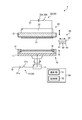
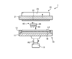
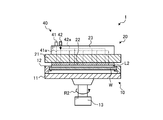
- FIG. 1 is a diagram showing an outline of the configuration of the plating processing apparatus 1 according to the embodiment.
- the semiconductor wafer W (hereinafter, referred to as “wafer W”) as the substrate to be processed is plated.
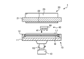
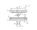
- the plating processing device 1 includes a substrate holding unit 10, a plating processing unit 20, a voltage applying unit 30, a processing liquid supply unit 40, and a control device 50.
- the substrate holding unit 10 holds the wafer W horizontally.
- the substrate holding portion 10 includes a substrate 11, a holding portion 12, and a drive mechanism 13.
- the substrate 11 is, for example, a spin chuck that holds and rotates the wafer W.
- the substrate 11 has a substantially disk shape and has a diameter larger than the diameter of the wafer W in a plan view.
- the holding portion 12 is provided on the upper surface of the substrate 11 and holds the wafer W from the side surface.
- the wafer W is horizontally held by the holding portion 12 in a state of being slightly separated from the upper surface of the substrate 11.
- the wafer W is held by the substrate holding portion 10 with the surface on which the substrate processing is performed facing upward.
- the holding portion 12 is provided with a cathode electrode (not shown). Then, when the wafer W is held by the holding portion 12, the cathode electrode comes into contact with the seed layer 62 (see FIG. 2C) on the surface of the wafer W.
- this cathode electrode is connected to a voltage application unit 30 described later, and a predetermined voltage can be applied to the seed layer 62 on the surface of the wafer W in contact with the cathode electrode.
- the substrate holding portion 10 is also provided with a drive mechanism 13 provided with a motor or the like, and the substrate 11 can be rotated to a predetermined speed. Further, the drive mechanism 13 is provided with an elevating drive unit (not shown) such as a cylinder, and the substrate 11 can be moved in the vertical direction.
- a drive mechanism 13 provided with a motor or the like, and the substrate 11 can be rotated to a predetermined speed. Further, the drive mechanism 13 is provided with an elevating drive unit (not shown) such as a cylinder, and the substrate 11 can be moved in the vertical direction.
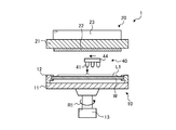
- the plating processing unit 20 includes a substrate 21, an anode electrode 22, and a moving mechanism 23.
- the base 21 is made of an insulating material.
- the substrate 21 has a substantially disk shape and has a diameter larger than the diameter of the wafer W in a plan view.
- the anode electrode 22 is made of a conductive material and is provided on the lower surface of the substrate 21.
- the anode electrode 22 is arranged so as to face substantially parallel to the wafer W held by the substrate holding portion 10.
- the anode electrode 22 comes into direct contact with the conductive liquid L2 (see FIG. 3B) supplied on the wafer W.
- the anode electrode 22 is connected to a voltage application unit 30 described later, and a predetermined voltage can be applied to the conductive liquid L2 in contact with the anode electrode 22.
- a moving mechanism 23 is provided on the upper surface side of the substrate 21.
- the moving mechanism 23 has, for example, an elevating drive unit (not shown) such as a cylinder. Then, the moving mechanism 23 can move the entire plating processing unit 20 in the vertical direction by the elevating drive unit.
- the voltage application unit 30 applies a predetermined voltage between the cathode electrode of the holding unit 12 and the anode electrode 22.
- the voltage application unit 30 includes, for example, a negative voltage application unit 31 and a positive voltage application unit 32.
- the negative voltage application unit 31 applies a negative voltage to the cathode electrode of the holding unit 12.
- the negative voltage application unit 31 has a DC power supply 31a and a switch 31b, and is connected to the cathode electrode of the holding unit 12. Specifically, the negative electrode side of the DC power supply 31a is connected to the cathode electrode of the holding portion 12 via the switch 31b, and the positive electrode side of the DC power supply 31a is grounded.
- the negative voltage applying unit 31 can apply a predetermined negative voltage to the cathode electrode of the holding unit 12.
- the positive voltage application unit 32 applies a positive voltage to the anode electrode 22.
- the positive voltage application unit 32 has a DC power supply 32a and a switch 32b, and is connected to the anode electrode 22. Specifically, the positive electrode side of the DC power supply 32a is connected to the anode electrode 22 via the switch 32b, and the negative electrode side of the DC power supply 32a is grounded.
- the positive voltage application unit 32 can apply a predetermined positive voltage to the anode electrode 22.
- the configuration of the voltage applying unit 30 is not limited to the example of FIG. 1, and any configuration can be used as long as a predetermined voltage can be applied between the cathode electrode and the anode electrode 22 of the holding unit 12. May be good.
- the processing liquid supply unit 40 is provided between the substrate holding unit 10 and the plating processing unit 20, and supplies various processing liquids onto the wafer W held by the substrate holding unit 10.
- the treatment liquid supply unit 40 includes a first supply unit 41, a second supply unit 42, a third supply unit 43, and a moving mechanism 44.
- the first supply unit 41 is, for example, a nozzle, and supplies the plating solution L1 (see FIG. 2B) onto the wafer W.
- the first supply unit 41 communicates with a plating solution supply source (not shown) that stores the plating solution L1.
- the processing liquid supply unit 40 can supply the plating liquid L1 from the plating liquid supply source to the first supply unit 41.
- the second supply unit 42 is, for example, a nozzle, and supplies the conductive liquid L2 (see FIG. 3A) on the wafer W.
- the second supply unit 42 communicates with a conductive liquid supply source (not shown) that stores the conductive liquid L2.
- the processing liquid supply unit 40 can supply the conductive liquid L2 from the conductive liquid supply source to the second supply unit 42.
- the third supply unit 43 is, for example, a nozzle, and supplies the cleaning liquid L3 (see FIG. 6) onto the wafer W.
- the third supply unit 43 communicates with a cleaning liquid supply source (not shown) that stores the cleaning liquid L3.
- the treatment liquid supply unit 40 can supply the cleaning liquid L3 from the cleaning liquid supply source to the third supply unit 43.
- the moving mechanism 44 can move the first supply unit 41, the second supply unit 42, and the third supply unit 43 in the horizontal direction and the vertical direction. That is, the first supply unit 41, the second supply unit 42, and the third supply unit 43 are configured to be freely advancing and retreating with respect to the substrate holding unit 10.
- the control device 50 is, for example, a computer, and has a control unit 51 and a storage unit 52.
- the control unit 51 includes a microcomputer having a CPU (Central Processing Unit), a ROM (Read Only Memory), a RAM (Random Access Memory), an input / output port, and various circuits.
- CPU Central Processing Unit
- ROM Read Only Memory
- RAM Random Access Memory
- the CPU of such a microcomputer By reading and executing the program stored in the ROM, the CPU of such a microcomputer reads and executes each part of the plating processing apparatus 1 such as the substrate holding unit 10, the plating processing unit 20, the voltage applying unit 30, and the processing liquid supply unit 40. Achieve control of.
- Such a program may be recorded on a storage medium readable by a computer, and may be installed from the storage medium in the storage unit 52 of the control device 50.
- Examples of storage media that can be read by a computer include a hard disk (HD), a flexible disk (FD), a compact disk (CD), a magnet optical disk (MO), and a memory card.
- the storage unit 52 is realized by, for example, a semiconductor memory element such as a RAM or a flash memory, or a storage device such as a hard disk or an optical disk.
- FIG. 2A is a diagram showing an outline of the substrate holding process and the first supply process according to the embodiment.
- the wafer W is conveyed to the substrate holding portion 10 by using a transfer mechanism (not shown). Then, the control unit 51 (see FIG. 1) operates the holding unit 12 to perform a substrate holding process for holding the wafer W in the substrate holding unit 10.
- FIG. 2C is a diagram showing a state of the wafer W after the first supply process according to the embodiment.
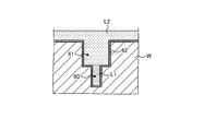
- the via 60 is formed, for example, at the bottom of the trench 61.
- the diameter of the via 60 is, for example, about 20 nm, and the width of the trench 61 is, for example, about 50 nm.
- an insulating layer such as SiO 2 (not shown), a barrier layer such as Ta or Ti (not shown), and a seed such as Cu, Co, or Ru are placed on the surface of the wafer W.
- Layers 62 are formed in order from the bottom.
- Ta may be used as the barrier layer and Cu may be used as the seed layer 62.
- the plating processing apparatus 1 performs a first supply process. Specifically, first, the control unit 51 moves the first supply unit 41 to the upper part of the central portion of the wafer W held by the substrate holding unit 10 by using the moving mechanism 44.
- control unit 51 transfers the plating solution L1 from the first supply unit 41 to the center of the wafer W while rotating the wafer W at a predetermined rotation speed R1 (for example, 50 to 200 rpm) using the drive mechanism 13. Supply.
- FIG. 2B is a diagram showing an outline of the first supply process according to the embodiment. Then, when the control unit 51 stops the supply of the plating solution L1 from the first supply unit 41, the first supply process ends.
- the inside of the via 60 and the trench 61 on the surface of the wafer W and the surface of the wafer W are filled with the plating solution L1.
- the plating solution L1 may contain copper ions and sulfate ions.
- the thickness of the plating solution L1 that has been first supplied is, for example, about 1 to 5 mm.
- FIG. 3A is a diagram showing an outline of the second supply process according to the embodiment. Specifically, first, the control unit 51 (see FIG. 1) moves the second supply unit 42 to above the central portion of the wafer W held by the substrate holding unit 10 by using the moving mechanism 44.
- control unit 51 supplies the conductive liquid L2 from the second supply unit 42 to the central portion of the wafer W while rotating the wafer W at a predetermined rotation speed R2 using the drive mechanism 13. Then, when the control unit 51 stops the supply of the conductive liquid L2 from the second supply unit 42, the second supply process ends.
- FIG. 3B is a diagram showing a state of the wafer W after the second supply process according to the embodiment.
- the inlet of the via 60 is narrower than that of the trench 61, the plating solution L1 is not easily extruded even if the second supply process is performed, and a large amount of the plating solution L1 remains inside the via 60.
- the conductive liquid L2 is a liquid having conductivity, and is, for example, a plating liquid having a lower content of a main component (for example, copper ions) than the plating liquid L1. Further, the conductive liquid L2 may be a liquid containing ammonia or CO 2 (that is, aqueous ammonia or a liquid containing CO 2 ). The thickness of the second supply-treated conductive liquid L2 is, for example, about 1 to 5 mm.
- the control unit 51 uses the moving mechanism 44 to separate the entire processing liquid supply unit 40 from above the wafer W. Further, in the substrate holding process, the first supply process, and the second supply process described so far, the plating processing unit 20 is arranged away from the substrate holding unit 10.
- FIG. 4A is a diagram showing an outline of the voltage application process according to the embodiment.
- control unit 51 uses the drive mechanism 13 to rotate the wafer W at a predetermined rotation speed R2, and uses the moving mechanism 23 to rotate the entire plating processing unit 20 into the wafer W.
- the anode electrode 22 is brought into contact with the conductive liquid L2 on the surface of the wafer W.
- control unit 51 changes the switch 31b and the switch 32b of the voltage application unit 30 from the off state to the on state while rotating the wafer W at a predetermined rotation speed R2 using the drive mechanism 13.
- the voltage application unit 30 applies a predetermined voltage between the wafer W and the conductive liquid L2.
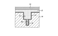
- FIG. 4B is a diagram showing a state of the wafer W after the voltage application process according to the embodiment.
- the plating film M is formed inside the trench 61 and on the surface of the wafer W. Can be suppressed.
- the plating film M is selectively formed inside the via 60 by further supplying the conductive liquid L2 onto the plating liquid L1 on the surface of the wafer W and then applying a predetermined voltage. can do.
- the control unit 51 uses the moving mechanism 23 to move the entire plating process unit 20 away from the wafer W.
- the first supply process, the second supply process, and the voltage application process may be sequentially repeated a predetermined number of times.
- FIG. 5 is a diagram showing a state of the wafer W after the first supply process, the second supply process, and the voltage application process according to the embodiment are sequentially repeated.
- the conductive liquid L2 has a smaller specific gravity than the plating liquid L1.
- the plating solution L1 having a large specific gravity tends to remain in the via 60 located at a position lower than the trench 61, and the plating solution L1 can be suppressed from being pushed out from the via 60.
- the specific gravity of the conductive liquid L2 is smaller than the specific gravity of the plating liquid L1, a liquid layer of the plating liquid L1 and the conductive liquid L2 is formed on the wafer W. It is possible to easily leave the plating solution L1 inside.
- the plating film M can be more selectively formed inside the via 60, the inside of the via 60 can be more satisfactorily filled with the plating film M.
- the embodiment it is preferable to use a plating solution having a content of a main component smaller than that of the plating solution L1 as the conductive liquid L2 having a specific gravity smaller than that of the plating solution L1.
- a plating solution having a content of a main component smaller than that of the plating solution L1 as the conductive liquid L2 having a specific gravity smaller than that of the plating solution L1.
- a liquid containing ammonia or CO 2 may be used as the conductive liquid L2 having a specific gravity smaller than that of the plating liquid L1.
- FIG. 6 is a diagram showing an outline of the substrate cleaning process according to the embodiment. Specifically, first, the control unit 51 (see FIG. 1) moves the third supply unit 43 to above the central portion of the wafer W held by the substrate holding unit 10 by using the moving mechanism 44.
- the control unit 51 supplies the cleaning liquid L3 from the third supply unit 43 to the central portion of the wafer W while rotating the wafer W at a predetermined rotation speed R3 (for example, 500 rpm or more) using the drive mechanism 13. .
- the cleaning liquid L3 is, for example, pure water. Then, when the control unit 51 stops the supply of the cleaning liquid L3 from the third supply unit 43, the substrate cleaning process is completed.
- the plating liquid L1 and the conductive liquid L2 supplied to the wafer W are washed away, and the surface of the wafer W is cleaned. As a result, the plating process according to the embodiment is completed.
- the plating solution reduction process for reducing the plating solution L1 on the surface of the wafer W may be performed.
- the rotation speed of the wafer W is increased from the rotation speed R2 to a predetermined rotation speed R4 (for example, 200 rpm) so that the plating solution L1 remains slightly on the surface of the wafer W. It can be carried out by shaking off.
- the concentration of the plating solution L1 inside the wafer W surface and the trench 61 can be reduced before the voltage application process, so that the plating film M is formed on the wafer W surface and inside the trench 61. Can be further suppressed.
- the plating film M can be more selectively formed inside the via 60, the inside of the via 60 can be more satisfactorily filled with the plating film M.
- a concentration reduction process for reducing the concentration of the plating solution L1 on the surface of the wafer W may be performed.
- This concentration reduction treatment can be carried out, for example, by supplying the cleaning liquid L3 or the like to the plating liquid L1 on the surface of the wafer W.
- the concentration of the plating solution L1 inside the wafer W surface and the trench 61 can be reduced before the voltage application treatment, so that the plating film M is formed on the wafer W surface and inside the trench 61. It can be further suppressed.
- the plating film M can be more selectively formed inside the via 60, the inside of the via 60 can be more satisfactorily filled with the plating film M.
- the wafer W after the plating treatment according to the embodiment, the wafer W may be subjected to the existing plating treatment or the like, and the inside of the trench 61 may be filled with the metal film Ma as shown in FIG.
- FIG. 7 is a diagram showing a state of the wafer W after all the processes are completed. As a result, a good multilayer wiring film can be formed on the wafer W.
- the anode electrode 22 having a size smaller than that of the wafer W may be provided in the plating processing unit 20, and the voltage application processing may be performed while scanning the anode electrode 22.
- FIG. 8 is a diagram showing an outline of the configuration of the plating processing apparatus 1 according to the modified example 1 of the embodiment. As shown in FIG. 8, in the first modification, the configurations of the plating processing unit 20 and the processing liquid supply unit 40 are different from those of the embodiment.
- the first supply unit 41 and the second supply unit 42 of the processing liquid supply unit 40 are provided in the plating processing unit 20 instead of the moving mechanism 44.
- the third supply unit 43 can be moved back and forth with respect to the substrate holding unit 10 by the moving mechanism 44 as in the embodiment.
- the flow path 41a for supplying the plating liquid L1 from the first supply unit 41 to the wafer W is formed in the plating processing unit 20, and the conductive liquid L2 from the second supply unit 42 is formed.
- the flow path 42a supplied to the wafer W is formed in the plating processing unit 20.
- FIG. 9 is a diagram showing an outline of the substrate holding process and the first supply process according to the first modification of the embodiment.
- the wafer W is conveyed to the substrate holding portion 10 by using a transfer mechanism (not shown). Then, the control unit 51 (see FIG. 8) operates the holding unit 12 to perform a substrate holding process for holding the wafer W in the substrate holding unit 10.
- the plating process device 1 of the modification 1 performs the first supply process. Specifically, first, the control unit 51 brings the entire plating processing unit 20 closer to the wafer W by using the moving mechanism 23.
- control unit 51 brings the entire plating unit 20 closer to the wafer W so that the distance between the wafer W and the anode electrode 22 is a predetermined distance (for example, 1 to 5 mm).
- control unit 51 uses the drive mechanism 13 to rotate the wafer W at a predetermined rotation speed R1 and between the wafer W and the anode electrode 22 from the first supply unit 41 via the flow path 41a.
- the plating solution L1 is supplied to the gap.
- control unit 51 changes the rotation speed of the wafer W to the rotation speed R2 when the plating solution L1 has spread over the entire surface of the wafer W, and continues the first supply process. Then, when the control unit 51 stops the supply of the plating solution L1 from the first supply unit 41, the first supply process ends.
- the inside of the via 60 and the trench 61 on the surface of the wafer W and the surface of the wafer W are filled with the plating solution L1.
- FIG. 10 is a diagram showing an outline of the second supply process according to the first modification of the embodiment.
- control unit 51 uses the drive mechanism 13 to rotate the wafer W at a predetermined rotation speed R2, and from the second supply unit 42 via the flow path 42a, the wafer W and the wafer W
- the conductive liquid L2 is supplied to the gap between the anode electrode 22 and the anode electrode 22.
- the plating liquid L1 liquid-filled on the surface of the wafer W is extruded by the conductive liquid L2, and the inside of the trench 61 and the surface of the wafer W are formed. Is approximately filled with the conductive liquid L2.
- the inlet of the via 60 is narrower than that of the trench 61, the plating solution L1 is not easily extruded even if the second supply process is performed, and a large amount of the plating solution L1 remains inside the via 60.
- FIG. 11 is a diagram showing an outline of the voltage application process according to the first modification of the embodiment.
- control unit 51 turns the wafer W at a predetermined rotation speed R2 by using the drive mechanism 13 while turning the switch 31b and the switch 32b of the voltage application unit 30 from the off state to the on state. Change to. As a result, the voltage application unit 30 applies a predetermined voltage between the wafer W and the conductive liquid L2.
- the inside of the trench 61 and the surface of the wafer W are plated. It is possible to suppress the formation of the film M.
- the plating film M is selectively formed inside the via 60 by further supplying the conductive liquid L2 onto the plating liquid L1 on the wafer W and then applying a predetermined voltage. Can be formed.
- the plating film M can be formed inside the via 60 without blocking the inlet of the via 60, so that the inside of the via 60 can be satisfactorily filled with the plating film M. ..
- the plating liquid L1 and the conductive liquid L2 can be supplied to the wafer W via the flow paths 41a and 42a formed in the plating processing unit 20.
- the processes from the first supply process to the voltage application process can be continuously performed without moving the plating processing unit 20.
- the time required for the plating process of the wafer W can be shortened.
- the post-treatment can be quickly performed after the first supply treatment, it is possible to prevent the seed layer 62 on the surface of the wafer W from being melted by the plating solution L1 until the post-treatment. Can be done.
- the processes from the first supply process to the voltage application process may be sequentially repeated.
- the plating film M can be selectively formed inside the via 60 a plurality of times, so that the inside of the via 60 can be firmly filled with the plating film M as shown in FIG. 5 of the embodiment.
- each process is performed without moving the plating processing unit 20 to another location. It can be repeated.
- the time required for the wafer W plating process can be shortened even when the processes from the first supply process to the voltage application process are sequentially repeated.
- the conductive liquid L2 has a smaller specific gravity than the plating liquid L1 as in the embodiment.
- the plating film M can be more selectively formed inside the via 60, so that the inside of the via 60 can be more satisfactorily filled with the plating film M.
- the modified example 1 it is preferable to use a plating solution having a content of a main component smaller than that of the plating solution L1 as the conductive liquid L2 having a specific gravity smaller than that of the plating solution L1.
- a plating solution having a content of a main component smaller than that of the plating solution L1 as the conductive liquid L2 having a specific gravity smaller than that of the plating solution L1.
- FIG. 12 is a diagram showing an outline of the substrate cleaning process according to the first modification of the embodiment.
- control unit 51 uses the moving mechanism 23 to separate the entire plating processing unit 20 from above the wafer W, and uses the moving mechanism 44 to separate the third supply unit 43.
- the wafer W held by the substrate holding portion 10 is moved to above the central portion.
- control unit 51 supplies the cleaning liquid L3 from the third supply unit 43 to the central portion of the wafer W while rotating the wafer W at a predetermined rotation speed R3 using the drive mechanism 13. Then, when the control unit 51 stops the supply of the cleaning liquid L3 from the third supply unit 43, the substrate cleaning process is completed.
- a plating solution reduction treatment or a concentration reduction treatment may be performed between the first supply treatment and the second supply treatment, as in the embodiment.
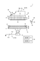
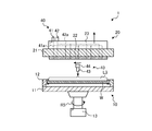
- FIG. 13 is a diagram showing an outline of the configuration of the plating processing apparatus 1 according to the second modification of the embodiment.
- the plating processing is performed using the bar nozzle-shaped plating processing unit 20.
- the plating processing section 20 of the modified example 2 has a rod-shaped substrate 21 extending in a direction substantially perpendicular to the traveling direction A. Then, in the plating processing unit 20, a plurality of suction ports 45b, a plurality of discharge ports 41b, a plurality of discharge ports 42b, an anode electrode 22, a plurality of suction ports 46b, and a plurality of suction ports 45b are provided below the substrate 21. A discharge port 43b is provided.
- the plurality of suction ports 45b are connected to the suction mechanism 45 via the flow path 45a.
- the plating processing unit 20 of the second modification can suck the treatment liquid or the like from the plurality of suction ports 45b.
- the plurality of discharge ports 41b are connected to the first supply unit 41 via the flow path 41a, and the plurality of discharge ports 42b are connected to the second supply unit 42 via the flow path 42a.
- the plurality of suction ports 46b are connected to the suction mechanism 46 via the flow path 46a.
- the plating processing unit 20 of the second modification can suck the treatment liquid or the like from the plurality of suction ports 46b.
- the plurality of discharge ports 43b are connected to the third supply unit 43 via the flow path 43a.
- the plurality of suction ports 45b, the plurality of discharge ports 41b, the plurality of discharge ports 42b, the plurality of suction ports 46b, and the plurality of discharge ports 43b are arranged side by side along the longitudinal direction of the substrate 21, respectively. .. Further, the anode electrode 22 is provided along the longitudinal direction of the substrate 21.
- control unit 51 scans the substrate 21 above the wafer W along the traveling direction A by using the moving mechanism 23.
- the plating liquid L1 is discharged from the plurality of discharge ports 41b, and the conductive liquid L2 is discharged above the plating liquid L1 from the plurality of discharge ports 41b located behind the plurality of discharge ports 41b. Discharge.
- the first supply processing and the second supply processing can be simultaneously performed on the surface of the wafer W.
- control unit 51 operates the voltage application unit 30 (see FIG. 1) to apply a negative potential to the cathode electrode of the holding unit 12 (see FIG. 1) and to apply a positive voltage to the anode electrode 22.
- control unit 51 can perform a voltage application process of applying a predetermined voltage between the wafer W and the conductive liquid L2 behind the plurality of discharge ports 42b.
- control unit 51 operates the suction mechanism 45 to suck the cleaning liquid L3 (see FIG. 6) located in front of the plating processing unit 20.
- the control unit 51 operates the suction mechanism 45 to suck the cleaning liquid L3 (see FIG. 6) located in front of the plating processing unit 20.
- control unit 51 operates the suction mechanism 46 to collect the plating liquid L1 and the conductive liquid L2 to which a predetermined voltage is applied from behind the anode electrode 22, and also operates the third supply unit 43. Then, the cleaning liquid L3 is discharged from the plurality of discharge ports 43b.
- the surface of the wafer W can be covered with the cleaning liquid L3, so that the cleanliness of the wafer W surface can be maintained with the cleaning liquid L3 without drying the surface of the wafer W.
- the first supply processing, the second supply processing, and the voltage application processing are performed while the wafer W is scanned in the traveling direction A by the bar nozzle-shaped plating processing unit 20. Can be done at the same time.
- the time required for the plating process of the wafer W can be shortened.
- the second modification since the first supply process, the second supply process, and the voltage application process can be performed at the same time, it is possible to prevent the seed layer 62 on the surface of the wafer W from being melted by the plating solution L1.
- the plating processing apparatus 1 includes a substrate holding unit 10, a first supply unit 41, a second supply unit 42, a voltage application unit 30, and a control unit 51.
- the substrate holding portion 10 holds the substrate (wafer W).
- the first supply unit 41 supplies the plating solution L1 onto the substrate (wafer W).
- the second supply unit 42 supplies a conductive liquid L2 different from the plating liquid L1 on the substrate (wafer W).
- the voltage application unit 30 applies a voltage.
- the control unit 51 controls each unit. Further, the control unit 51 holds the substrate (wafer W) by the substrate holding unit 10, and supplies the plating solution L1 on the held substrate (wafer W) by the first supply unit 41.
- control unit 51 supplies the conductive liquid L2 on the plating solution L1 supplied to the substrate (wafer W) by the second supply unit 42, and supplies the substrate (wafer W) and the conductive liquid by the voltage application unit 30.
- a voltage is applied between L2 and L2.
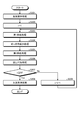
- FIG. 14 is a flowchart showing a procedure of plating processing executed by the plating processing apparatus 1 according to the embodiment.
- control unit 51 controls the substrate holding unit 10 and the like to perform a substrate holding process in which the holding unit 12 holds the wafer W (step S101). Then, the control unit 51 sets 1 in the counter n for counting the number of repetitions of the plating process (step S102).
- control unit 51 controls the processing liquid supply unit 40 and the like to perform the first supply process of supplying the plating solution L1 from the first supply unit 41 to the surface of the wafer W (step S103). Then, the control unit 51 controls the processing liquid supply unit 40 and the like to carry out the second supply process of supplying the conductive liquid L2 from the second supply unit 42 to the surface of the wafer W (step S104).
- control unit 51 controls the plating processing unit 20, the voltage application unit 30, and the like to perform a voltage application process of applying a predetermined voltage between the wafer W and the conductive liquid L2 (step S105). ..
- control unit 51 determines whether or not the counter n is N or more a predetermined number of times (step S106). Information about the predetermined number of times N is stored in advance in the storage unit 52.
- control unit 51 controls the processing liquid supply unit 40 and the like to apply the cleaning liquid L3 from the third supply unit 43 to the surface of the wafer W.
- the substrate cleaning process to be supplied is performed (step S107), and the process is completed.
- step S106 when the counter n is not equal to or greater than the predetermined number of times N (steps S106, No), the control unit 51 increments the counter n for counting the number of repetitions of the plating process (step S108), and the process of step S103. Return to.
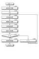
- FIG. 15 is a flowchart showing another procedure of the plating process executed by the plating process device 1 according to the embodiment.
- control unit 51 controls the substrate holding unit 10 and the like to perform a substrate holding process in which the holding unit 12 holds the wafer W (step S201). Then, the control unit 51 sets 1 in the counter n for counting the number of repetitions of the plating process (step S202).
- control unit 51 controls the processing liquid supply unit 40 and the like to perform the first supply process of supplying the plating solution L1 from the first supply unit 41 to the surface of the wafer W (step S203). Then, the control unit 51 controls the substrate holding unit 10 and the like to perform a plating solution reduction process of reducing the plating solution L1 on the surface of the wafer W (step S204).
- control unit 51 controls the processing liquid supply unit 40 and the like to perform a second supply process of supplying the conductive liquid L2 from the second supply unit 42 to the surface of the wafer W (step S205).
- control unit 51 controls the plating processing unit 20, the voltage application unit 30, and the like to perform a voltage application process of applying a predetermined voltage between the wafer W and the conductive liquid L2 (step S206). ..
- control unit 51 determines whether or not the counter n is N or more a predetermined number of times (step S207). When the counter n is N or more a predetermined number of times (steps S207, Yes), the control unit 51 controls the processing liquid supply unit 40 and the like to apply the cleaning liquid L3 from the third supply unit 43 to the surface of the wafer W. The substrate cleaning process to be supplied is performed (step S208), and the process is completed.
- step S207 and No when the counter n is not equal to or greater than the predetermined number of times N (steps S207 and No), the control unit 51 increments the counter n for counting the number of repetitions of the plating process (step S209), and processes in step S203. Return to.
- FIG. 16 is a flowchart showing another procedure of the plating process executed by the plating process device 1 according to the embodiment.
- control unit 51 controls the substrate holding unit 10 and the like to perform a substrate holding process in which the holding unit 12 holds the wafer W (step S301). Then, the control unit 51 sets 1 to the counter n for counting the number of repetitions of the plating process (step S302).
- control unit 51 controls the processing liquid supply unit 40 and the like to perform the first supply process of supplying the plating solution L1 from the first supply unit 41 to the surface of the wafer W (step S303). Then, the control unit 51 controls the processing liquid supply unit 40 and the like to perform a concentration reduction process for reducing the concentration of the plating solution L1 on the surface of the wafer W (step S304).
- control unit 51 controls the processing liquid supply unit 40 and the like to perform a second supply process of supplying the conductive liquid L2 from the second supply unit 42 to the surface of the wafer W (step S305).
- control unit 51 controls the plating processing unit 20, the voltage application unit 30, and the like to perform a voltage application process of applying a predetermined voltage between the wafer W and the conductive liquid L2 (step S306). ..
- control unit 51 determines whether or not the counter n is N or more a predetermined number of times (step S307).
- the control unit 51 controls the processing liquid supply unit 40 and the like to apply the cleaning liquid L3 from the third supply unit 43 to the surface of the wafer W.
- the substrate cleaning process to be supplied is performed (step S308), and the process is completed.
- step S307, No when the counter n is not equal to or greater than the predetermined number of times N (step S307, No), the control unit 51 increments the counter n for counting the number of repetitions of the plating process (step S309), and the process of step S303. Return to.
- the plating treatment method includes a substrate holding step, a first supply step, a second supply step, and a voltage application step.
- the substrate holding step (steps S101, S201, S301) holds the substrate (wafer W).
- the plating solution L1 is supplied onto the held substrate (wafer W).
- the second supply step (steps S104, S205, S305)
- a conductive liquid L2 different from the plating liquid L1 is supplied onto the plating liquid L1 supplied to the substrate (wafer W).
- the voltage application step steps S105, S206, S306), a voltage is applied between the substrate (wafer W) and the conductive liquid L2.
- the inside of the via 60 can be satisfactorily filled with the plating film M.
- the plating treatment method according to the embodiment further includes a plating solution reducing step (step S204) for reducing the plating solution L1 on the substrate (wafer W) after the first supply step (step S203).
- a plating solution reducing step step S204 for reducing the plating solution L1 on the substrate (wafer W) after the first supply step (step S203).
- the plating treatment method according to the embodiment further includes a concentration reducing step (step S304) for reducing the concentration of the plating solution L1 after the first supply step (step S303).
- a concentration reducing step step S304 for reducing the concentration of the plating solution L1 after the first supply step (step S303).
- each step from the first supply step (steps S103, S203, S303) to the voltage application step (steps S105, S206, S306) is sequentially repeated.
- the inside of the via 60 can be firmly filled with the plating film M.
- the conductive liquid L2 has a smaller specific gravity than the plating liquid L1. As a result, the inside of the via 60 can be more satisfactorily filled with the plating film M.
- the conductive liquid L2 is a plating liquid having a lower content of the main component than the plating liquid L1.
- the conductive liquid L2 is a liquid containing ammonia or CO 2. As a result, it is possible to prevent the surface of the wafer W from being contaminated or an unintended reactant being generated due to the conductive liquid L2 during the voltage application process.
- the present disclosure is not limited to the above embodiments, and various changes can be made as long as the purpose is not deviated.
- an example in which the wafer W in which the via 60 is formed at the bottom of the trench 61 is plated, but the wafer W in which the thin via 60 is formed on the surface is plated in the present disclosure. Treatment may be applied.
Landscapes
- Chemical & Material Sciences (AREA)
- Engineering & Computer Science (AREA)
- Chemical Kinetics & Catalysis (AREA)
- Electrochemistry (AREA)
- Materials Engineering (AREA)
- Metallurgy (AREA)
- Organic Chemistry (AREA)
- Life Sciences & Earth Sciences (AREA)
- Sustainable Development (AREA)
- Automation & Control Theory (AREA)
- Electroplating Methods And Accessories (AREA)
- Electrodes Of Semiconductors (AREA)
- Internal Circuitry In Semiconductor Integrated Circuit Devices (AREA)
Abstract
Description
開示の実施形態は、めっき処理方法およびめっき処理装置に関する。 The disclosed embodiment relates to a plating treatment method and a plating treatment apparatus.
従来、基板である半導体ウェハ(以下、ウェハと呼称する。)をスピンチャックで保持しながらめっき処理を行い、ウェハの表面にめっき膜を形成する方法が知られている(たとえば、特許文献1参照)。 Conventionally, there is known a method of forming a plating film on the surface of a wafer by performing a plating process while holding a semiconductor wafer (hereinafter, referred to as a wafer) as a substrate with a spin chuck (see, for example, Patent Document 1). ).
本開示は、ビアの内部をめっき膜で良好に埋めることができる技術を提供する。 The present disclosure provides a technique capable of satisfactorily filling the inside of a via with a plating film.
本開示の一態様によるめっき処理方法は、基板保持工程と、第1供給工程と、第2供給工程と、電圧印加工程とを含む。基板保持工程は、基板を保持する。第1供給工程は、保持された前記基板上にめっき液を供給する。第2供給工程は、前記基板に供給された前記めっき液上に、前記めっき液とは異なる導電性液体を供給する。電圧印加工程は、前記基板と前記導電性液体との間に電圧を印加する。 The plating treatment method according to one aspect of the present disclosure includes a substrate holding step, a first supply step, a second supply step, and a voltage application step. The substrate holding step holds the substrate. In the first supply step, the plating solution is supplied onto the held substrate. In the second supply step, a conductive liquid different from the plating liquid is supplied onto the plating liquid supplied to the substrate. In the voltage application step, a voltage is applied between the substrate and the conductive liquid.
本開示によれば、ビアの内部をめっき膜で良好に埋めることができる。 According to the present disclosure, the inside of the via can be satisfactorily filled with the plating film.
以下、添付図面を参照して、本願の開示するめっき処理方法およびめっき処理装置の実施形態を詳細に説明する。なお、以下に示す実施形態により本開示が限定されるものではない。また、図面は模式的なものであり、各要素の寸法の関係、各要素の比率などは、現実と異なる場合があることに留意する必要がある。さらに、図面の相互間においても、互いの寸法の関係や比率が異なる部分が含まれている場合がある。 Hereinafter, the plating treatment method and the embodiment of the plating treatment apparatus disclosed in the present application will be described in detail with reference to the attached drawings. The present disclosure is not limited by the embodiments shown below. In addition, it should be noted that the drawings are schematic, and the dimensional relationship of each element, the ratio of each element, and the like may differ from the reality. Further, even between the drawings, there may be parts having different dimensional relationships and ratios from each other.
従来、基板である半導体ウェハ(以下、ウェハと呼称する。)をスピンチャックで保持しながらめっき処理を行い、ウェハの表面にめっき膜を形成する方法が知られている。 Conventionally, there is known a method of forming a plating film on the surface of a wafer by performing a plating process while holding a semiconductor wafer (hereinafter referred to as a wafer) as a substrate with a spin chuck.
しかしながら、従来のめっき処理では、ウェハの表面に形成されるトレンチの底部にさらにビアが形成される場合に、トレンチ内でめっき膜が成長することでビアの入口が塞がれてしまう場合があった。これにより、ビアの内部をめっき膜で埋めることができない恐れがあった。 However, in the conventional plating process, when more vias are formed at the bottom of the trench formed on the surface of the wafer, the inlet of the vias may be blocked by the growth of the plating film in the trench. rice field. As a result, there is a risk that the inside of the via cannot be filled with the plating film.
そこで、上述の問題点を克服し、ビアの内部をめっき膜で良好に埋めることができる技術が期待されている。 Therefore, a technology that can overcome the above-mentioned problems and satisfactorily fill the inside of the via with a plating film is expected.
<めっき処理装置の構成>
最初に、図1を参照しながら、実施形態に係るめっき処理装置1の構成について説明する。図1は、実施形態に係るめっき処理装置1の構成の概略を示す図である。
<Structure of plating processing equipment>
First, the configuration of the
かかるめっき処理装置1では、被処理基板としての半導体ウェハW(以下、「ウェハW」と呼称する。)に対してめっき処理を行う。めっき処理装置1は、基板保持部10と、めっき処理部20と、電圧印加部30と、処理液供給部40と、制御装置50とを備える。
In the
基板保持部10は、ウェハWを水平に保持する。基板保持部10は、基体11と、保持部12と、駆動機構13とを有する。基体11は、たとえば、ウェハWを保持して回転させるスピンチャックである。基体11は、略円板状であり、平面視においてウェハWの径よりも大きい径を有する。
The
保持部12は、基体11の上面に設けられ、ウェハWを側面から保持する。ウェハWは、かかる保持部12によって基体11の上面からわずかに離間した状態で水平保持される。なお、ウェハWは、基板処理が行われる表面を上方に向けた状態で基板保持部10に保持される。
The
また、保持部12には、カソード電極(図示せず)が設けられる。そして、保持部12でウェハWを保持する際に、かかるカソード電極がウェハW表面のシード層62(図2C参照)と接触する。
Further, the
さらに、このカソード電極は、後述する電圧印加部30に接続されており、接触するウェハW表面のシード層62に所定の電圧を印加することができる。
Further, this cathode electrode is connected to a
基板保持部10には、また、モータなどを備えた駆動機構13が設けられており、基体11を所定の速度に回転させることができる。また、駆動機構13には、シリンダなどの昇降駆動部(図示せず)が設けられており、基体11を鉛直方向に移動させることができる。
The
ここまで説明した基板保持部10の上方には、基体11の上面に向かい合って、めっき処理部20が設けられる。めっき処理部20は、基体21と、アノード電極22と、移動機構23とを有する。
Above the
基体21は、絶縁性材料で構成される。基体21は、略円板状であり、平面視においてウェハWの径より大きい径を有する。
The
アノード電極22は、導電性材料で構成され、基体21の下面に設けられる。アノード電極22は、基板保持部10に保持されるウェハWと略平行に向かい合うように配置される。
The
そして、電圧印加処理を行う際、アノード電極22は、ウェハW上に供給された導電性液体L2(図3B参照)と直接接触する。アノード電極22は、後述する電圧印加部30に接続されており、接触する導電性液体L2に所定の電圧を印加することができる。
Then, when performing the voltage application process, the
基体21の上面側には、移動機構23が設けられる。移動機構23は、たとえば、シリンダなどの昇降駆動部(図示せず)を有する。そして、移動機構23は、かかる昇降駆動部により、めっき処理部20全体を鉛直方向に移動させることができる。
A moving
電圧印加部30は、保持部12のカソード電極と、アノード電極22との間に所定の電圧を印加する。電圧印加部30は、たとえば、負電圧印加部31と、正電圧印加部32とを有する。
The
負電圧印加部31は、保持部12のカソード電極に負電圧を印加する。負電圧印加部31は、直流電源31aと、スイッチ31bとを有し、保持部12のカソード電極に接続される。具体的には、直流電源31aの負極側が、スイッチ31bを介して保持部12のカソード電極に接続されるとともに、直流電源31aの正極側が接地される。
The negative
そして、スイッチ31bをオン状態に制御することにより、負電圧印加部31は、保持部12のカソード電極に所定の負電圧を印加することができる。
Then, by controlling the
正電圧印加部32は、アノード電極22に正電圧を印加する。正電圧印加部32は、直流電源32aと、スイッチ32bとを有し、アノード電極22に接続される。具体的には、直流電源32aの正極側が、スイッチ32bを介してアノード電極22に接続されるとともに、直流電源32aの負極側が接地される。
The positive
そして、スイッチ32bをオン状態に制御することにより、正電圧印加部32は、アノード電極22に所定の正電圧を印加することができる。
Then, by controlling the
なお、電圧印加部30の構成は図1の例に限られず、保持部12のカソード電極とアノード電極22との間に所定の電圧を印加可能な構成であれば、どのような構成であってもよい。
The configuration of the
処理液供給部40は、基板保持部10とめっき処理部20との間に設けられ、基板保持部10に保持されたウェハW上に各種の処理液を供給する。処理液供給部40は、第1供給部41と、第2供給部42と、第3供給部43と、移動機構44とを有する。
The processing
第1供給部41は、たとえばノズルであり、ウェハW上にめっき液L1(図2B参照)を供給する。第1供給部41は、めっき液L1を貯留するめっき液供給源(図示せず)と連通する。これにより、処理液供給部40は、かかるめっき液供給源から第1供給部41にめっき液L1を供給することができる。
The
第2供給部42は、たとえばノズルであり、ウェハW上に導電性液体L2(図3A参照)を供給する。第2供給部42は、導電性液体L2を貯留する導電性液体供給源(図示せず)と連通する。これにより、処理液供給部40は、かかる導電性液体供給源から第2供給部42に導電性液体L2を供給することができる。
The
第3供給部43は、たとえばノズルであり、ウェハW上に洗浄液L3(図6参照)を供給する。第3供給部43は、洗浄液L3を貯留する洗浄液供給源(図示せず)と連通する。これにより、処理液供給部40は、かかる洗浄液供給源から第3供給部43に洗浄液L3を供給することができる。
The
移動機構44は、第1供給部41、第2供給部42および第3供給部43を水平方向および鉛直方向に移動させることができる。すなわち、第1供給部41、第2供給部42および第3供給部43は、基板保持部10に対して進退自在に構成される。
The moving
制御装置50は、たとえばコンピュータであり、制御部51と記憶部52とを有する。制御部51は、CPU(Central Processing Unit)、ROM(Read Only Memory)、RAM(Random Access Memory)、入出力ポートなどを有するマイクロコンピュータや各種の回路を含む。
The
かかるマイクロコンピュータのCPUは、ROMに記憶されているプログラムを読み出して実行することにより、基板保持部10やめっき処理部20、電圧印加部30、処理液供給部40などのめっき処理装置1における各部の制御を実現する。
By reading and executing the program stored in the ROM, the CPU of such a microcomputer reads and executes each part of the
なお、かかるプログラムは、コンピュータによって読み取り可能な記憶媒体に記録されていたものであって、その記憶媒体から制御装置50の記憶部52にインストールされたものであってもよい。コンピュータによって読み取り可能な記憶媒体としては、たとえばハードディスク(HD)、フレキシブルディスク(FD)、コンパクトディスク(CD)、マグネットオプティカルディスク(MO)、メモリカードなどがある。
Note that such a program may be recorded on a storage medium readable by a computer, and may be installed from the storage medium in the storage unit 52 of the
記憶部52は、たとえば、RAM、フラッシュメモリ(Flash Memory)などの半導体メモリ素子、または、ハードディスク、光ディスクなどの記憶装置によって実現される。 The storage unit 52 is realized by, for example, a semiconductor memory element such as a RAM or a flash memory, or a storage device such as a hard disk or an optical disk.
<めっき処理の詳細>
つづいて、図2A~図7を参照しながら、実施形態に係るめっき処理装置1で行うめっき処理の詳細について説明する。実施形態に係るめっき処理では、最初に、基板保持処理および第1供給処理が行われる。図2Aは、実施形態に係る基板保持処理および第1供給処理の概要を示す図である。
<Details of plating process>
Subsequently, the details of the plating process performed by the
まず、図示しない搬送機構を用いて、ウェハWを基板保持部10に搬送する。そして、制御部51(図1参照)は、保持部12を動作させることにより、ウェハWを基板保持部10に保持する基板保持処理を行う。
First, the wafer W is conveyed to the
なお、かかる基板保持処理に先だって、ウェハWの表面には、図2Cに示すように、ビア60およびトレンチ61が形成される。図2Cは、実施形態に係る第1供給処理後のウェハWの状態を示す図である。
Prior to the substrate holding process, vias 60 and
実施形態において、ビア60は、たとえば、トレンチ61の底部に形成される。ビア60の直径は、たとえば20nm程度であり、トレンチ61の幅は、たとえば50nm程度である。
In the embodiment, the via 60 is formed, for example, at the bottom of the
また、基板保持処理に先だって、ウェハWの表面には、SiO2などの絶縁層(図示せず)と、TaやTiなどのバリア層(図示せず)と、CuやCo、Ruなどのシード層62とが下から順に成膜される。なお、めっき膜M(図4B参照)としてCu膜を形成する場合、バリア層としてはTaを、シード層62としてはCuを用いるとよい。
Further, prior to the substrate holding process, an insulating layer such as SiO 2 (not shown), a barrier layer such as Ta or Ti (not shown), and a seed such as Cu, Co, or Ru are placed on the surface of the wafer W. Layers 62 are formed in order from the bottom. When forming a Cu film as the plating film M (see FIG. 4B), Ta may be used as the barrier layer and Cu may be used as the
図2Aの説明に戻る。基板保持処理につづいて、めっき処理装置1では、第1供給処理が行われる。具体的には、まず、制御部51が、移動機構44を用いて第1供給部41を基板保持部10に保持されたウェハWにおける中心部の上方まで移動させる。
Return to the explanation of Fig. 2A. Following the substrate holding process, the
次に、制御部51は、駆動機構13を用いてウェハWを所定の回転数R1(たとえば、50~200rpm)で回転させながら、第1供給部41からめっき液L1をウェハWの中心部に供給する。
Next, the control unit 51 transfers the plating solution L1 from the
さらに、制御部51は、ウェハWの全面にめっき液L1が行き渡ったところで、図2Bに示すように、ウェハWの回転数を回転数R2(たとえば、2~10rpm)に変化させて、第1供給処理を継続する。図2Bは、実施形態に係る第1供給処理の概要を示す図である。そして、制御部51が第1供給部41からのめっき液L1の供給を停止させると、第1供給処理が終了する。
Further, when the plating solution L1 has spread over the entire surface of the wafer W, the control unit 51 changes the rotation speed of the wafer W to the rotation speed R2 (for example, 2 to 10 rpm) as shown in FIG. 2B, and first Continue supply processing. FIG. 2B is a diagram showing an outline of the first supply process according to the embodiment. Then, when the control unit 51 stops the supply of the plating solution L1 from the
かかる第1供給処理によって、図2Cに示すように、ウェハW表面のビア60およびトレンチ61の内部と、ウェハWの表面とがめっき液L1で満たされる。
By the first supply process, as shown in FIG. 2C, the inside of the via 60 and the
たとえば、めっき膜M(図4B参照)としてCu膜を形成する場合、めっき液L1には、銅イオンと硫酸イオンとが含まれるとよい。また、第1供給処理されためっき液L1の厚さは、たとえば、1~5mm程度である。 For example, when a Cu film is formed as the plating film M (see FIG. 4B), the plating solution L1 may contain copper ions and sulfate ions. The thickness of the plating solution L1 that has been first supplied is, for example, about 1 to 5 mm.
第1供給処理につづいて、実施形態に係るめっき処理では、第2供給処理が行われる。図3Aは、実施形態に係る第2供給処理の概要を示す図である。具体的には、まず、制御部51(図1参照)が、移動機構44を用いて第2供給部42を基板保持部10に保持されたウェハWにおける中心部の上方まで移動させる。
Following the first supply process, the second supply process is performed in the plating process according to the embodiment. FIG. 3A is a diagram showing an outline of the second supply process according to the embodiment. Specifically, first, the control unit 51 (see FIG. 1) moves the
次に、制御部51は、駆動機構13を用いてウェハWを所定の回転数R2で回転させながら、第2供給部42から導電性液体L2をウェハWの中心部に供給する。そして、制御部51が第2供給部42からの導電性液体L2の供給を停止させると、第2供給処理が終了する。
Next, the control unit 51 supplies the conductive liquid L2 from the
かかる第2供給処理によって、図3Bに示すように、ウェハW表面に液盛りされていためっき液L1が導電性液体L2により押し出されて、トレンチ61の内部とウェハWの表面とが導電性液体L2でおおよそ満たされる。図3Bは、実施形態に係る第2供給処理後のウェハWの状態を示す図である。
By such a second supply process, as shown in FIG. 3B, the plating liquid L1 liquid-filled on the surface of the wafer W is extruded by the conductive liquid L2, and the inside of the
一方で、ビア60はトレンチ61よりも入口が狭いことから、第2供給処理を行ってもめっき液L1は容易には押し出されず、ビア60の内部にはめっき液L1が多く残る。
On the other hand, since the inlet of the via 60 is narrower than that of the
導電性液体L2は、導電性を有する液体であり、たとえば、めっき液L1よりも主成分(たとえば、銅イオン)の含有量が少ないめっき液である。また、導電性液体L2は、アンモニアまたはCO2を含有する液体(すなわち、アンモニア水またはCO2含有液)であってもよい。また、第2供給処理された導電性液体L2の厚さは、たとえば、1~5mm程度である。 The conductive liquid L2 is a liquid having conductivity, and is, for example, a plating liquid having a lower content of a main component (for example, copper ions) than the plating liquid L1. Further, the conductive liquid L2 may be a liquid containing ammonia or CO 2 (that is, aqueous ammonia or a liquid containing CO 2 ). The thickness of the second supply-treated conductive liquid L2 is, for example, about 1 to 5 mm.
なお、導電性液体L2をウェハWに供給した後に、制御部51は、移動機構44を用いて処理液供給部40全体をウェハWの上方から離脱させる。また、ここまで説明した基板保持処理、第1供給処理および第2供給処理において、めっき処理部20は、基板保持部10から離れて配置される。
After supplying the conductive liquid L2 to the wafer W, the control unit 51 uses the moving
第2供給処理につづいて、実施形態に係るめっき処理では、電圧印加処理が行われる。図4Aは、実施形態に係る電圧印加処理の概要を示す図である。 Following the second supply process, the voltage application process is performed in the plating process according to the embodiment. FIG. 4A is a diagram showing an outline of the voltage application process according to the embodiment.
具体的には、まず、制御部51(図1参照)が、駆動機構13を用いてウェハWを所定の回転数R2で回転させながら、移動機構23を用いてめっき処理部20全体をウェハWに近づけて、アノード電極22をウェハW表面の導電性液体L2に接触させる。
Specifically, first, the control unit 51 (see FIG. 1) uses the
次に、制御部51は、駆動機構13を用いてウェハWを所定の回転数R2で回転させながら、電圧印加部30のスイッチ31bおよびスイッチ32bをオフ状態からオン状態に変更する。
Next, the control unit 51 changes the
これにより、保持部12のカソード電極に負電位が印加されるとともに、アノード電極22に正電圧が印加される。このように、電圧印加処理によって、電圧印加部30は、ウェハWと導電性液体L2との間に所定の電圧を印加する。
As a result, a negative potential is applied to the cathode electrode of the holding
これにより、導電性液体L2を介してめっき液L1の内部に電界が形成され、ビア60の表面側に正の荷電粒子である銅イオンが集積されることから、図4Bに示すように、ビア60の内部にめっき膜Mが形成される。図4Bは、実施形態に係る電圧印加処理後のウェハWの状態を示す図である。 As a result, an electric field is formed inside the plating liquid L1 via the conductive liquid L2, and copper ions, which are positively charged particles, are accumulated on the surface side of the via 60. Therefore, as shown in FIG. 4B, the via A plating film M is formed inside the 60. FIG. 4B is a diagram showing a state of the wafer W after the voltage application process according to the embodiment.
一方で、実施形態に係る電圧印加処理では、トレンチ61の内部やウェハWの表面に残るめっき液L1の量が少ないことから、トレンチ61の内部やウェハWの表面にめっき膜Mが形成されることを抑制することができる。
On the other hand, in the voltage application process according to the embodiment, since the amount of the plating solution L1 remaining inside the
すなわち、実施形態に係るめっき処理では、ウェハW表面のめっき液L1上にさらに導電性液体L2を供給した後に所定の電圧を印加することにより、ビア60の内部に選択的にめっき膜Mを形成することができる。 That is, in the plating process according to the embodiment, the plating film M is selectively formed inside the via 60 by further supplying the conductive liquid L2 onto the plating liquid L1 on the surface of the wafer W and then applying a predetermined voltage. can do.
したがって、実施形態によれば、ビア60の入口が塞がれることなくビア60の内部にめっき膜Mを形成することができることから、ビア60の内部をめっき膜Mで良好に埋めることができる。なお、電圧印加処理を行った後に、制御部51は、移動機構23を用いてめっき処理部20全体をウェハWから遠ざける。
Therefore, according to the embodiment, since the plating film M can be formed inside the via 60 without blocking the entrance of the via 60, the inside of the via 60 can be satisfactorily filled with the plating film M. After performing the voltage application process, the control unit 51 uses the moving
また、実施形態では、第1供給処理、第2供給処理および電圧印加処理を、所定の回数、順次繰り返して実施するとよい。 Further, in the embodiment, the first supply process, the second supply process, and the voltage application process may be sequentially repeated a predetermined number of times.
これにより、ビア60の内部に選択的にめっき膜Mを複数回形成することができることから、図5に示すように、ビア60の内部をめっき膜Mでしっかり埋めることができる。図5は、実施形態に係る第1供給処理、第2供給処理および電圧印加処理を順次繰り返して行った後のウェハWの状態を示す図である。 As a result, the plating film M can be selectively formed a plurality of times inside the via 60, so that the inside of the via 60 can be firmly filled with the plating film M as shown in FIG. FIG. 5 is a diagram showing a state of the wafer W after the first supply process, the second supply process, and the voltage application process according to the embodiment are sequentially repeated.
また、実施形態では、導電性液体L2が、めっき液L1よりも比重が小さいとよい。これにより、トレンチ61よりも低い箇所に位置するビア60に比重が大きいめっき液L1が残りやすくなるとともに、ビア60からめっき液L1が押し出されることを抑制することができる。
Further, in the embodiment, it is preferable that the conductive liquid L2 has a smaller specific gravity than the plating liquid L1. As a result, the plating solution L1 having a large specific gravity tends to remain in the via 60 located at a position lower than the
また、実施形態では、導電性液体L2の比重がめっき液L1の比重よりも小さいことにより、ウェハW上にめっき液L1と導電性液体L2との液層が形成されることから、ビア60の内部にめっき液L1を残しやすくすることができる。 Further, in the embodiment, since the specific gravity of the conductive liquid L2 is smaller than the specific gravity of the plating liquid L1, a liquid layer of the plating liquid L1 and the conductive liquid L2 is formed on the wafer W. It is possible to easily leave the plating solution L1 inside.
したがって、実施形態によれば、ビア60の内部にさらに選択的にめっき膜Mを形成することができることから、ビア60の内部をめっき膜Mでさらに良好に埋めることができる。 Therefore, according to the embodiment, since the plating film M can be more selectively formed inside the via 60, the inside of the via 60 can be more satisfactorily filled with the plating film M.
また、実施形態では、めっき液L1よりも比重の小さい導電性液体L2として、めっき液L1よりも主成分の含有量が少ないめっき液を用いるとよい。これにより、電圧印加処理の際に、導電性液体L2に起因してウェハWの表面が汚染されたり、意図しない反応物が生成されることなどを抑制することができる。 Further, in the embodiment, it is preferable to use a plating solution having a content of a main component smaller than that of the plating solution L1 as the conductive liquid L2 having a specific gravity smaller than that of the plating solution L1. As a result, it is possible to prevent the surface of the wafer W from being contaminated or an unintended reactant being generated due to the conductive liquid L2 during the voltage application process.
また、実施形態では、めっき液L1よりも比重の小さい導電性液体L2として、アンモニアまたはCO2を含有する液体を用いてもよい。 Further, in the embodiment, a liquid containing ammonia or CO 2 may be used as the conductive liquid L2 having a specific gravity smaller than that of the plating liquid L1.
実施形態に係るめっき処理では、ビア60の内部がめっき膜Mで埋まった後に、基板洗浄処理が行われる。図6は、実施形態に係る基板洗浄処理の概要を示す図である。具体的には、まず、制御部51(図1参照)が、移動機構44を用いて第3供給部43を基板保持部10に保持されたウェハWにおける中心部の上方まで移動させる。
In the plating process according to the embodiment, the substrate cleaning process is performed after the inside of the via 60 is filled with the plating film M. FIG. 6 is a diagram showing an outline of the substrate cleaning process according to the embodiment. Specifically, first, the control unit 51 (see FIG. 1) moves the
次に、制御部51は、駆動機構13を用いてウェハWを所定の回転数R3(たとえば、500rpm以上)で回転させながら、第3供給部43から洗浄液L3をウェハWの中心部に供給する。洗浄液L3は、たとえば、純水である。そして、制御部51が第3供給部43からの洗浄液L3の供給を停止させると、基板洗浄処理が終了する。
Next, the control unit 51 supplies the cleaning liquid L3 from the
かかる基板洗浄処理によって、ウェハWに供給されていためっき液L1や導電性液体L2などが洗い流されて、ウェハWの表面が洗浄される。これにより、実施形態に係るめっき処理が完了する。 By such a substrate cleaning process, the plating liquid L1 and the conductive liquid L2 supplied to the wafer W are washed away, and the surface of the wafer W is cleaned. As a result, the plating process according to the embodiment is completed.
また、実施形態では、第1供給処理を行ってウェハWの表面にめっき液L1を供給した後に、ウェハW表面のめっき液L1を減少させるめっき液減少処理を実施してもよい。このめっき液減少処理は、たとえば、ウェハWの回転数を回転数R2から所定の回転数R4(たとえば、200rpm)に増加させて、めっき液L1がウェハWの表面に多少残る程度にめっき液L1を振り切ることで実施することができる。 Further, in the embodiment, after the first supply process is performed to supply the plating solution L1 to the surface of the wafer W, the plating solution reduction process for reducing the plating solution L1 on the surface of the wafer W may be performed. In this plating solution reduction treatment, for example, the rotation speed of the wafer W is increased from the rotation speed R2 to a predetermined rotation speed R4 (for example, 200 rpm) so that the plating solution L1 remains slightly on the surface of the wafer W. It can be carried out by shaking off.
かかるめっき液減少処理により、電圧印加処理の前にウェハW表面やトレンチ61内部のめっき液L1の濃度を減少させることができることから、ウェハW表面やトレンチ61内部でめっき膜Mが形成されることをさらに抑制することができる。
By such a plating solution reducing process, the concentration of the plating solution L1 inside the wafer W surface and the
したがって、実施形態によれば、ビア60の内部にさらに選択的にめっき膜Mを形成することができることから、ビア60の内部をめっき膜Mでさらに良好に埋めることができる。 Therefore, according to the embodiment, since the plating film M can be more selectively formed inside the via 60, the inside of the via 60 can be more satisfactorily filled with the plating film M.
また、実施形態では、第1供給処理を行ってウェハWの表面にめっき液L1を供給した後に、ウェハW表面のめっき液L1の濃度を低下させる濃度低下処理を実施してもよい。この濃度低下処理は、たとえば、ウェハW表面のめっき液L1に対して洗浄液L3などを供給することで実施することができる。 Further, in the embodiment, after the first supply process is performed to supply the plating solution L1 to the surface of the wafer W, a concentration reduction process for reducing the concentration of the plating solution L1 on the surface of the wafer W may be performed. This concentration reduction treatment can be carried out, for example, by supplying the cleaning liquid L3 or the like to the plating liquid L1 on the surface of the wafer W.
かかる濃度低下処理により、電圧印加処理の前にウェハW表面やトレンチ61内部のめっき液L1の濃度を減少させることができることから、ウェハW表面やトレンチ61内部でめっき膜Mが形成されることをさらに抑制することができる。
By such a concentration reduction treatment, the concentration of the plating solution L1 inside the wafer W surface and the
したがって、実施形態によれば、ビア60の内部にさらに選択的にめっき膜Mを形成することができることから、ビア60の内部をめっき膜Mでさらに良好に埋めることができる。 Therefore, according to the embodiment, since the plating film M can be more selectively formed inside the via 60, the inside of the via 60 can be more satisfactorily filled with the plating film M.
なお、本開示では、実施形態に係るめっき処理を行った後に、ウェハWに既存のめっき処理などを施して、図7に示すように、トレンチ61の内部を金属膜Maで埋めてもよい。図7は、すべての処理を完了した後のウェハWの状態を示す図である。これにより、ウェハWに良好な多層配線膜を形成することができる。
In the present disclosure, after the plating treatment according to the embodiment, the wafer W may be subjected to the existing plating treatment or the like, and the inside of the
また、本開示では、ウェハWよりもサイズの小さいアノード電極22をめっき処理部20に設け、かかるアノード電極22をスキャンさせながら電圧印加処理を行ってもよい。
Further, in the present disclosure, the
<各種変形例>
つづいて、実施形態の各種変形例について、図8~図13を参照しながら説明する。なお、以下の各種変形例において、実施形態と同一の部位には同一の符号を付することにより重複する説明を省略する。
<Various deformation examples>
Subsequently, various modifications of the embodiment will be described with reference to FIGS. 8 to 13. In the following various modifications, duplicate description will be omitted by assigning the same reference numerals to the same parts as those in the embodiment.
図8は、実施形態の変形例1に係るめっき処理装置1の構成の概略を示す図である。図8に示すように、変形例1では、めっき処理部20および処理液供給部40の構成が実施形態と異なる。
FIG. 8 is a diagram showing an outline of the configuration of the
具体的には、変形例1に係るめっき処理装置1では、処理液供給部40のうち、第1供給部41および第2供給部42が移動機構44ではなくめっき処理部20に設けられる。一方で、第3供給部43は、実施形態と同様、移動機構44によって基板保持部10に対して進退自在に移動可能である。
Specifically, in the
また、変形例1では、第1供給部41からのめっき液L1をウェハWに供給する流路41aがめっき処理部20内に形成されるとともに、第2供給部42からの導電性液体L2をウェハWに供給する流路42aがめっき処理部20内に形成される。
Further, in the first modification, the
次に、変形例1に係るめっき処理装置1で行うめっき処理の詳細について説明する。図9は、実施形態の変形例1に係る基板保持処理および第1供給処理の概要を示す図である。
Next, the details of the plating process performed by the
まず、図示しない搬送機構を用いて、ウェハWを基板保持部10に搬送する。そして、制御部51(図8参照)は、保持部12を動作させることにより、ウェハWを基板保持部10に保持する基板保持処理を行う。
First, the wafer W is conveyed to the
かかる基板保持処理につづいて、変形例1のめっき処理装置1では、第1供給処理が行われる。具体的には、まず、制御部51が、移動機構23を用いてめっき処理部20全体をウェハWに近づける。
Following the substrate holding process, the
この際、制御部51は、ウェハWとアノード電極22との間隔が所定の間隔(たとえば、1~5mm)となるように、めっき処理部20全体をウェハWに近づける。
At this time, the control unit 51 brings the
次に、制御部51は、駆動機構13を用いてウェハWを所定の回転数R1で回転させながら、第1供給部41から流路41aを介して、ウェハWとアノード電極22との間の隙間にめっき液L1を供給する。
Next, the control unit 51 uses the
さらに、制御部51は、ウェハWの全面にめっき液L1が行き渡ったところで、ウェハWの回転数を回転数R2に変化させて、第1供給処理を継続する。そして、制御部51が第1供給部41からのめっき液L1の供給を停止させると、第1供給処理が終了する。
Further, the control unit 51 changes the rotation speed of the wafer W to the rotation speed R2 when the plating solution L1 has spread over the entire surface of the wafer W, and continues the first supply process. Then, when the control unit 51 stops the supply of the plating solution L1 from the
かかる第1供給処理によって、実施形態の図2Cに示したように、ウェハW表面のビア60およびトレンチ61の内部と、ウェハWの表面とがめっき液L1で満たされる。
By the first supply process, as shown in FIG. 2C of the embodiment, the inside of the via 60 and the
第1供給処理につづいて、変形例1に係るめっき処理では、第2供給処理が行われる。図10は、実施形態の変形例1に係る第2供給処理の概要を示す図である。 Following the first supply process, the second supply process is performed in the plating process according to the first modification. FIG. 10 is a diagram showing an outline of the second supply process according to the first modification of the embodiment.
具体的には、制御部51(図8参照)が、駆動機構13を用いてウェハWを所定の回転数R2で回転させながら、第2供給部42から流路42aを介して、ウェハWとアノード電極22との間の隙間に導電性液体L2を供給する。
Specifically, the control unit 51 (see FIG. 8) uses the
そして、制御部51が第2供給部42からの導電性液体L2の供給を停止させると、第2供給処理が終了する。
Then, when the control unit 51 stops the supply of the conductive liquid L2 from the
かかる第2供給処理によって、実施形態の図3Bに示したように、ウェハW表面に液盛りされていためっき液L1が導電性液体L2により押し出されて、トレンチ61の内部とウェハWの表面とが導電性液体L2でおおよそ満たされる。
By such a second supply process, as shown in FIG. 3B of the embodiment, the plating liquid L1 liquid-filled on the surface of the wafer W is extruded by the conductive liquid L2, and the inside of the
一方で、ビア60はトレンチ61よりも入口が狭いことから、第2供給処理を行ってもめっき液L1は容易には押し出されず、ビア60の内部にはめっき液L1が多く残る。
On the other hand, since the inlet of the via 60 is narrower than that of the
第2供給処理につづいて、変形例1に係るめっき処理では、電圧印加処理が行われる。図11は、実施形態の変形例1に係る電圧印加処理の概要を示す図である。 Following the second supply process, a voltage application process is performed in the plating process according to the first modification. FIG. 11 is a diagram showing an outline of the voltage application process according to the first modification of the embodiment.
具体的には、制御部51(図8参照)が、駆動機構13を用いてウェハWを所定の回転数R2で回転させながら、電圧印加部30のスイッチ31bおよびスイッチ32bをオフ状態からオン状態に変更する。これにより、電圧印加部30は、ウェハWと導電性液体L2との間に所定の電圧を印加する。
Specifically, the control unit 51 (see FIG. 8) turns the wafer W at a predetermined rotation speed R2 by using the
これにより、導電性液体L2を介してめっき液L1の内部に電界が形成され、ビア60の表面側に正の荷電粒子である銅イオンが集積されることから、実施形態の図4Bに示したように、ビア60の内部にめっき膜Mが形成される。 As a result, an electric field is formed inside the plating liquid L1 via the conductive liquid L2, and copper ions, which are positively charged particles, are accumulated on the surface side of the via 60, which is shown in FIG. 4B of the embodiment. As described above, the plating film M is formed inside the via 60.
さらに、変形例1に係る電圧印加処理では、実施形態と同様に、トレンチ61の内部やウェハWの表面に残るめっき液L1の量が少ないことから、トレンチ61の内部やウェハWの表面にめっき膜Mが形成されることを抑制することができる。
Further, in the voltage application process according to the first modification, since the amount of the plating solution L1 remaining inside the
すなわち、変形例1に係るめっき処理では、ウェハW上のめっき液L1上にさらに導電性液体L2を供給した後に所定の電圧を印加することにより、ビア60の内部に選択的にめっき膜Mを形成することができる。 That is, in the plating process according to the first modification, the plating film M is selectively formed inside the via 60 by further supplying the conductive liquid L2 onto the plating liquid L1 on the wafer W and then applying a predetermined voltage. Can be formed.
したがって、変形例1によれば、ビア60の入口が塞がれることなくビア60の内部にめっき膜Mを形成することができることから、ビア60の内部をめっき膜Mで良好に埋めることができる。 Therefore, according to the first modification, the plating film M can be formed inside the via 60 without blocking the inlet of the via 60, so that the inside of the via 60 can be satisfactorily filled with the plating film M. ..
また、変形例1では、めっき処理部20に形成される流路41a、42aを介してめっき液L1および導電性液体L2をウェハWに供給可能である。これにより、変形例1では、めっき処理部20を移動させることなく、第1供給処理から電圧印加処理までの処理を連続的に行うことができる。
Further, in the modified example 1, the plating liquid L1 and the conductive liquid L2 can be supplied to the wafer W via the
したがって、変形例1によれば、ウェハWのめっき処理にかかる時間を短縮することができる。 Therefore, according to the first modification, the time required for the plating process of the wafer W can be shortened.
さらに、変形例1では、第1供給処理の後にすばやく後の処理を実施することができることから、後の処理までの間にめっき液L1によってウェハW表面のシード層62が溶けることを抑制することができる。
Further, in the first modification, since the post-treatment can be quickly performed after the first supply treatment, it is possible to prevent the
また、変形例1では、電圧印加処理を行った後に、第1供給処理から電圧印加処理までの処理を順次繰り返して行うとよい。これにより、ビア60の内部に選択的にめっき膜Mを複数回形成することができることから、実施形態の図5に示したように、ビア60の内部をめっき膜Mでしっかり埋めることができる。 Further, in the modified example 1, after the voltage application process is performed, the processes from the first supply process to the voltage application process may be sequentially repeated. As a result, the plating film M can be selectively formed inside the via 60 a plurality of times, so that the inside of the via 60 can be firmly filled with the plating film M as shown in FIG. 5 of the embodiment.
なお、電圧印加処理を行った後に、第1供給処理から電圧印加処理までの処理を順次繰り返して行う場合、変形例1では、めっき処理部20を別の場所に移動させることなく、各処理を繰り返して行うことができる。
When the processes from the first supply process to the voltage application process are sequentially repeated after the voltage application process is performed, in the first modification, each process is performed without moving the
すなわち、変形例1では、第1供給処理から電圧印加処理までの処理を順次繰り返して行う場合でも、ウェハWのめっき処理にかかる時間を短縮することができる。 That is, in the first modification, the time required for the wafer W plating process can be shortened even when the processes from the first supply process to the voltage application process are sequentially repeated.
また、変形例1では、実施形態と同様に、導電性液体L2が、めっき液L1よりも比重が小さいとよい。これにより、ビア60の内部にさらに選択的にめっき膜Mを形成することができることから、ビア60の内部をめっき膜Mでさらに良好に埋めることができる。 Further, in the modified example 1, it is preferable that the conductive liquid L2 has a smaller specific gravity than the plating liquid L1 as in the embodiment. As a result, the plating film M can be more selectively formed inside the via 60, so that the inside of the via 60 can be more satisfactorily filled with the plating film M.
また、変形例1では、実施形態と同様に、めっき液L1よりも比重の小さい導電性液体L2として、めっき液L1よりも主成分の含有量が少ないめっき液を用いるとよい。これにより、電圧印加処理の際に、導電性液体L2に起因してウェハWの表面が汚染されたり、意図しない反応物が生成されることなどを抑制することができる。 Further, in the modified example 1, as in the embodiment, it is preferable to use a plating solution having a content of a main component smaller than that of the plating solution L1 as the conductive liquid L2 having a specific gravity smaller than that of the plating solution L1. As a result, it is possible to prevent the surface of the wafer W from being contaminated or an unintended reactant being generated due to the conductive liquid L2 during the voltage application process.
変形例1に係るめっき処理では、ビア60の内部がめっき膜Mで埋まった後に、基板洗浄処理が行われる。図12は、実施形態の変形例1に係る基板洗浄処理の概要を示す図である。 In the plating process according to the first modification, the substrate cleaning process is performed after the inside of the via 60 is filled with the plating film M. FIG. 12 is a diagram showing an outline of the substrate cleaning process according to the first modification of the embodiment.
具体的には、まず、制御部51(図8参照)が、移動機構23を用いてめっき処理部20全体をウェハWの上方から離脱させるとともに、移動機構44を用いて第3供給部43を基板保持部10に保持されたウェハWにおける中心部の上方まで移動させる。
Specifically, first, the control unit 51 (see FIG. 8) uses the moving
次に、制御部51は、駆動機構13を用いてウェハWを所定の回転数R3で回転させながら、第3供給部43から洗浄液L3をウェハWの中心部に供給する。そして、制御部51が第3供給部43からの洗浄液L3の供給を停止させると、基板洗浄処理が終了する。
Next, the control unit 51 supplies the cleaning liquid L3 from the
なお、ここまで説明した変形例1では、実施形態と同様に、第1供給処理と第2供給処理との間にめっき液減少処理や濃度低下処理を実施してもよい。 In the modified example 1 described so far, a plating solution reduction treatment or a concentration reduction treatment may be performed between the first supply treatment and the second supply treatment, as in the embodiment.
図13は、実施形態の変形例2に係るめっき処理装置1の構成の概略を示す図である。変形例2に係るめっき処理装置1では、バーノズル状のめっき処理部20を用いてめっき処理を行う。
FIG. 13 is a diagram showing an outline of the configuration of the
変形例2のめっき処理部20は、進行方向Aと略垂直な方向に延びる棒状の基体21を有する。そして、かかるめっき処理部20には、基体21の下部に複数の吸引口45bと、複数の吐出口41bと、複数の吐出口42bと、アノード電極22と、複数の吸引口46bと、複数の吐出口43bとが設けられる。
The
複数の吸引口45bは、流路45aを介して吸引機構45に接続される。変形例2のめっき処理部20は、かかる吸引機構45を動作させることにより、複数の吸引口45bから処理液などを吸引することができる。
The plurality of
複数の吐出口41bは、流路41aを介して第1供給部41に接続され、複数の吐出口42bは、流路42aを介して第2供給部42に接続される。
The plurality of
また、複数の吸引口46bは、流路46aを介して吸引機構46に接続される。変形例2のめっき処理部20は、かかる吸引機構46を動作させることにより、複数の吸引口46bから処理液などを吸引することができる。複数の吐出口43bは、流路43aを介して第3供給部43に接続される。
Further, the plurality of
複数の吸引口45bと、複数の吐出口41bと、複数の吐出口42bと、複数の吸引口46bと、複数の吐出口43bとは、それぞれ基体21の長手方向に沿って並んで配置される。また、アノード電極22は、基体21の長手方向に沿って設けられる。
The plurality of
さらに、基体21の下部には、進行方向Aの前側から順に、複数の吸引口45b、複数の吐出口41b、複数の吐出口42b、アノード電極22、複数の吸引口46bおよび複数の吐出口43bが設けられる。
Further, in the lower part of the
つづいて、変形例2のめっき処理装置1で行うめっき処理について説明する。まず、制御部51(図1参照)は、移動機構23を用いて、基体21を進行方向Aに沿ってウェハWの上方でスキャンさせる。
Next, the plating process performed by the
そして、変形例2では、複数の吐出口41bからめっき液L1を吐出するとともに、かかる複数の吐出口41bの後方に位置する複数の吐出口41bから、導電性液体L2をめっき液L1の上方に吐出する。
Then, in the second modification, the plating liquid L1 is discharged from the plurality of
これにより、変形例2に係るめっき処理装置1では、ウェハWの表面に対して第1供給処理および第2供給処理を同時に行うことができる。
As a result, in the
また、制御部51は、電圧印加部30(図1参照)を動作させて、保持部12(図1参照)のカソード電極に負電位を印加するとともに、アノード電極22に正電圧を印加する。これにより、制御部51は、複数の吐出口42bの後方で、ウェハWと導電性液体L2との間に所定の電圧を印加する電圧印加処理を行うことができる。
Further, the control unit 51 operates the voltage application unit 30 (see FIG. 1) to apply a negative potential to the cathode electrode of the holding unit 12 (see FIG. 1) and to apply a positive voltage to the
また、制御部51は、吸引機構45を動作させて、めっき処理部20の前方に位置する洗浄液L3(図6参照)などを吸引する。これにより、ウェハWの表面に洗浄液L3などが存在していたとしても、かかる洗浄液によってめっき液L1が薄まることを抑制することができる。したがって、変形例2によれば、めっき処理を安定して実施することができる。
Further, the control unit 51 operates the
また、制御部51は、吸引機構46を動作させて、所定の電圧が印加されためっき液L1および導電性液体L2を、アノード電極22の後方から回収するとともに、第3供給部43を動作させて、複数の吐出口43bから洗浄液L3を吐出する。
Further, the control unit 51 operates the
これにより、ウェハWの表面を洗浄液L3で覆うことができることから、ウェハWの表面を乾燥させることなく、洗浄液L3でウェハW表面の清浄度を保つことができる。 As a result, the surface of the wafer W can be covered with the cleaning liquid L3, so that the cleanliness of the wafer W surface can be maintained with the cleaning liquid L3 without drying the surface of the wafer W.
ここまで説明したように、変形例2のめっき処理装置1では、バーノズル状のめっき処理部20でウェハWを進行方向Aにスキャンしながら、第1供給処理、第2供給処理および電圧印加処理を同時に行うことができる。
As described above, in the
したがって、変形例2によれば、ウェハWのめっき処理にかかる時間を短縮することができる。 Therefore, according to the modified example 2, the time required for the plating process of the wafer W can be shortened.
さらに、変形例2では、第1供給処理、第2供給処理および電圧印加処理を同時に実施することができることから、めっき液L1によってウェハW表面のシード層62が溶けることを抑制することができる。
Further, in the second modification, since the first supply process, the second supply process, and the voltage application process can be performed at the same time, it is possible to prevent the
実施形態に係るめっき処理装置1は、基板保持部10と、第1供給部41と、第2供給部42と、電圧印加部30と、制御部51とを備える。基板保持部10は、基板(ウェハW)を保持する。第1供給部41は、基板(ウェハW)上にめっき液L1を供給する。第2供給部42は、基板(ウェハW)上にめっき液L1とは異なる導電性液体L2を供給する。電圧印加部30は、電圧を印加する。制御部51は各部を制御する。また、制御部51は、基板保持部10によって基板(ウェハW)を保持し、保持された基板(ウェハW)上に第1供給部41によってめっき液L1を供給する。さらに、制御部51は、基板(ウェハW)に供給されためっき液L1上に、第2供給部42によって導電性液体L2を供給し、電圧印加部30によって基板(ウェハW)と導電性液体L2との間に電圧を印加する。これにより、ビア60の内部をめっき膜Mで良好に埋めることができる。
The
<処理の手順>
つづいて、実施形態に係る基板処理の手順について、図14~図16を参照しながら説明する。図14は、実施形態に係るめっき処理装置1が実行するめっき処理の手順を示すフローチャートである。
<Processing procedure>
Subsequently, the procedure of the substrate processing according to the embodiment will be described with reference to FIGS. 14 to 16. FIG. 14 is a flowchart showing a procedure of plating processing executed by the
最初に、制御部51は、基板保持部10などを制御して、保持部12にウェハWを保持させる基板保持処理を実施する(ステップS101)。そして、制御部51は、めっき処理の繰り返し数をカウントするためのカウンタnに1を設定する(ステップS102)。
First, the control unit 51 controls the
次に、制御部51は、処理液供給部40などを制御して、第1供給部41からめっき液L1をウェハWの表面に供給する第1供給処理を実施する(ステップS103)。そして、制御部51は、処理液供給部40などを制御して、第2供給部42から導電性液体L2をウェハWの表面に供給する第2供給処理を実施する(ステップS104)。
Next, the control unit 51 controls the processing
次に、制御部51は、めっき処理部20や電圧印加部30などを制御して、ウェハWと導電性液体L2との間に所定の電圧を印加する電圧印加処理を実施する(ステップS105)。
Next, the control unit 51 controls the
次に、制御部51は、カウンタnが所定の回数N以上であるか否かを判定する(ステップS106)。なお、かかる所定の回数Nに関する情報は、記憶部52にあらかじめ記憶されている。 Next, the control unit 51 determines whether or not the counter n is N or more a predetermined number of times (step S106). Information about the predetermined number of times N is stored in advance in the storage unit 52.
そして、カウンタnが所定の回数N以上である場合(ステップS106,Yes)、制御部51は、処理液供給部40などを制御して、第3供給部43から洗浄液L3をウェハWの表面に供給する基板洗浄処理を実施し(ステップS107)、処理を完了する。
When the counter n is N or more a predetermined number of times (steps S106, Yes), the control unit 51 controls the processing
一方で、カウンタnが所定の回数N以上ではない場合(ステップS106,No)、制御部51は、めっき処理の繰り返し数をカウントするためのカウンタnをインクリメントし(ステップS108)、ステップS103の処理に戻る。 On the other hand, when the counter n is not equal to or greater than the predetermined number of times N (steps S106, No), the control unit 51 increments the counter n for counting the number of repetitions of the plating process (step S108), and the process of step S103. Return to.
図15は、実施形態に係るめっき処理装置1が実行するめっき処理の別の手順を示すフローチャートである。
FIG. 15 is a flowchart showing another procedure of the plating process executed by the
最初に、制御部51は、基板保持部10などを制御して、保持部12にウェハWを保持させる基板保持処理を実施する(ステップS201)。そして、制御部51は、めっき処理の繰り返し数をカウントするためのカウンタnに1を設定する(ステップS202)。
First, the control unit 51 controls the
次に、制御部51は、処理液供給部40などを制御して、第1供給部41からめっき液L1をウェハWの表面に供給する第1供給処理を実施する(ステップS203)。そして、制御部51は、基板保持部10などを制御して、ウェハW表面のめっき液L1を減少させるめっき液減少処理を実施する(ステップS204)。
Next, the control unit 51 controls the processing
次に、制御部51は、処理液供給部40などを制御して、第2供給部42から導電性液体L2をウェハWの表面に供給する第2供給処理を実施する(ステップS205)。
Next, the control unit 51 controls the processing
次に、制御部51は、めっき処理部20や電圧印加部30などを制御して、ウェハWと導電性液体L2との間に所定の電圧を印加する電圧印加処理を実施する(ステップS206)。
Next, the control unit 51 controls the
次に、制御部51は、カウンタnが所定の回数N以上であるか否かを判定する(ステップS207)。そして、カウンタnが所定の回数N以上である場合(ステップS207,Yes)、制御部51は、処理液供給部40などを制御して、第3供給部43から洗浄液L3をウェハWの表面に供給する基板洗浄処理を実施し(ステップS208)、処理を完了する。
Next, the control unit 51 determines whether or not the counter n is N or more a predetermined number of times (step S207). When the counter n is N or more a predetermined number of times (steps S207, Yes), the control unit 51 controls the processing
一方で、カウンタnが所定の回数N以上ではない場合(ステップS207,No)、制御部51は、めっき処理の繰り返し数をカウントするためのカウンタnをインクリメントし(ステップS209)、ステップS203の処理に戻る。 On the other hand, when the counter n is not equal to or greater than the predetermined number of times N (steps S207 and No), the control unit 51 increments the counter n for counting the number of repetitions of the plating process (step S209), and processes in step S203. Return to.
図16は、実施形態に係るめっき処理装置1が実行するめっき処理の別の手順を示すフローチャートである。
FIG. 16 is a flowchart showing another procedure of the plating process executed by the
最初に、制御部51は、基板保持部10などを制御して、保持部12にウェハWを保持させる基板保持処理を実施する(ステップS301)。そして、制御部51は、めっき処理の繰り返し数をカウントするためのカウンタnに1を設定する(ステップS302)。
First, the control unit 51 controls the
次に、制御部51は、処理液供給部40などを制御して、第1供給部41からめっき液L1をウェハWの表面に供給する第1供給処理を実施する(ステップS303)。そして、制御部51は、処理液供給部40などを制御して、ウェハW表面のめっき液L1の濃度を低下させる濃度低下処理を実施する(ステップS304)。
Next, the control unit 51 controls the processing
次に、制御部51は、処理液供給部40などを制御して、第2供給部42から導電性液体L2をウェハWの表面に供給する第2供給処理を実施する(ステップS305)。
Next, the control unit 51 controls the processing
次に、制御部51は、めっき処理部20や電圧印加部30などを制御して、ウェハWと導電性液体L2との間に所定の電圧を印加する電圧印加処理を実施する(ステップS306)。
Next, the control unit 51 controls the
次に、制御部51は、カウンタnが所定の回数N以上であるか否かを判定する(ステップS307)。そして、カウンタnが所定の回数N以上である場合(ステップS307,Yes)、制御部51は、処理液供給部40などを制御して、第3供給部43から洗浄液L3をウェハWの表面に供給する基板洗浄処理を実施し(ステップS308)、処理を完了する。
Next, the control unit 51 determines whether or not the counter n is N or more a predetermined number of times (step S307). When the counter n is N or more a predetermined number of times (steps S307, Yes), the control unit 51 controls the processing
一方で、カウンタnが所定の回数N以上ではない場合(ステップS307,No)、制御部51は、めっき処理の繰り返し数をカウントするためのカウンタnをインクリメントし(ステップS309)、ステップS303の処理に戻る。 On the other hand, when the counter n is not equal to or greater than the predetermined number of times N (step S307, No), the control unit 51 increments the counter n for counting the number of repetitions of the plating process (step S309), and the process of step S303. Return to.
実施形態に係るめっき処理方法は、基板保持工程と、第1供給工程と、第2供給工程と、電圧印加工程とを含む。基板保持工程(ステップS101、S201、S301)は、基板(ウェハW)を保持する。第1供給工程(ステップS103、S203、S303)は、保持された基板(ウェハW)上にめっき液L1を供給する。第2供給工程(ステップS104、S205、S305)は、基板(ウェハW)に供給されためっき液L1上に、めっき液L1とは異なる導電性液体L2を供給する。電圧印加工程(ステップS105、S206、S306)は、基板(ウェハW)と導電性液体L2との間に電圧を印加する。これにより、ビア60の内部をめっき膜Mで良好に埋めることができる。 The plating treatment method according to the embodiment includes a substrate holding step, a first supply step, a second supply step, and a voltage application step. The substrate holding step (steps S101, S201, S301) holds the substrate (wafer W). In the first supply step (steps S103, S203, S303), the plating solution L1 is supplied onto the held substrate (wafer W). In the second supply step (steps S104, S205, S305), a conductive liquid L2 different from the plating liquid L1 is supplied onto the plating liquid L1 supplied to the substrate (wafer W). In the voltage application step (steps S105, S206, S306), a voltage is applied between the substrate (wafer W) and the conductive liquid L2. As a result, the inside of the via 60 can be satisfactorily filled with the plating film M.
また、実施形態に係るめっき処理方法は、第1供給工程(ステップS203)の後に、基板(ウェハW)上のめっき液L1を減少させるめっき液減少工程(ステップS204)をさらに含む。これにより、ビア60の内部をめっき膜Mでさらに良好に埋めることができる。 Further, the plating treatment method according to the embodiment further includes a plating solution reducing step (step S204) for reducing the plating solution L1 on the substrate (wafer W) after the first supply step (step S203). As a result, the inside of the via 60 can be more satisfactorily filled with the plating film M.
また、実施形態に係るめっき処理方法は、第1供給工程(ステップS303)の後に、めっき液L1の濃度を低下させる濃度低下工程(ステップS304)をさらに含む。これにより、ビア60の内部をめっき膜Mでさらに良好に埋めることができる。 Further, the plating treatment method according to the embodiment further includes a concentration reducing step (step S304) for reducing the concentration of the plating solution L1 after the first supply step (step S303). As a result, the inside of the via 60 can be more satisfactorily filled with the plating film M.
また、実施形態に係るめっき処理方法において、第1供給工程(ステップS103、S203、S303)から電圧印加工程(ステップS105、S206、S306)までの各工程は、順次繰り返して行われる。これにより、ビア60の内部をめっき膜Mでしっかり埋めることができる。 Further, in the plating processing method according to the embodiment, each step from the first supply step (steps S103, S203, S303) to the voltage application step (steps S105, S206, S306) is sequentially repeated. As a result, the inside of the via 60 can be firmly filled with the plating film M.
また、実施形態に係るめっき処理方法において、導電性液体L2は、めっき液L1よりも比重が小さい。これにより、ビア60の内部をめっき膜Mでさらに良好に埋めることができる。 Further, in the plating treatment method according to the embodiment, the conductive liquid L2 has a smaller specific gravity than the plating liquid L1. As a result, the inside of the via 60 can be more satisfactorily filled with the plating film M.
また、実施形態に係るめっき処理方法において、導電性液体L2は、めっき液L1よりも主成分の含有量が少ないめっき液である。これにより、電圧印加処理の際に、導電性液体L2に起因してウェハWの表面が汚染されたり、意図しない反応物が生成されることなどを抑制することができる。 Further, in the plating treatment method according to the embodiment, the conductive liquid L2 is a plating liquid having a lower content of the main component than the plating liquid L1. As a result, it is possible to prevent the surface of the wafer W from being contaminated or an unintended reactant being generated due to the conductive liquid L2 during the voltage application process.
また、実施形態に係るめっき処理方法において、導電性液体L2は、アンモニアまたはCO2を含有する液体である。これにより、電圧印加処理の際に、導電性液体L2に起因してウェハWの表面が汚染されたり、意図しない反応物が生成されることなどを抑制することができる。 Further, in the plating treatment method according to the embodiment, the conductive liquid L2 is a liquid containing ammonia or CO 2. As a result, it is possible to prevent the surface of the wafer W from being contaminated or an unintended reactant being generated due to the conductive liquid L2 during the voltage application process.
以上、本開示の実施形態について説明したが、本開示は上記実施形態に限定されるものではなく、その趣旨を逸脱しない限りにおいて種々の変更が可能である。たとえば、上記の実施形態では、トレンチ61の底部にビア60が形成されたウェハWにめっき処理を施す例について示したが、表面に細いビア60が形成されたウェハWなどに、本開示のめっき処理を施してもよい。
Although the embodiments of the present disclosure have been described above, the present disclosure is not limited to the above embodiments, and various changes can be made as long as the purpose is not deviated. For example, in the above embodiment, an example in which the wafer W in which the via 60 is formed at the bottom of the
今回開示された実施形態は全ての点で例示であって制限的なものではないと考えられるべきである。実に、上記した実施形態は多様な形態で具現され得る。また、上記の実施形態は、添付の請求の範囲及びその趣旨を逸脱することなく、様々な形態で省略、置換、変更されてもよい。 The embodiments disclosed this time should be considered to be exemplary in all respects and not restrictive. Indeed, the above embodiments can be embodied in a variety of forms. Further, the above-described embodiment may be omitted, replaced or changed in various forms without departing from the scope of the appended claims and the purpose thereof.
W ウェハ
1 めっき処理装置
10 基板保持部
20 めっき処理部
30 電圧印加部
40 処理液供給部
41 第1供給部
42 第2供給部
43 第3供給部
L1 めっき液
L2 導電性液体
L3 洗浄液
Claims (8)
保持された前記基板上にめっき液を供給する第1供給工程と、
前記基板に供給された前記めっき液上に、前記めっき液とは異なる導電性液体を供給する第2供給工程と、
前記基板と前記導電性液体との間に電圧を印加する電圧印加工程と、
を含むめっき処理方法。 The board holding process for holding the board and
The first supply step of supplying the plating solution onto the held substrate, and
A second supply step of supplying a conductive liquid different from the plating liquid onto the plating liquid supplied to the substrate, and
A voltage application step of applying a voltage between the substrate and the conductive liquid,
Plating method including.
請求項1に記載のめっき処理方法。 The plating treatment method according to claim 1, further comprising a plating solution reducing step of reducing the plating solution on the substrate after the first supply step.
請求項1に記載のめっき処理方法。 The plating treatment method according to claim 1, further comprising a concentration reducing step of reducing the concentration of the plating solution after the first supply step.
請求項1~3のいずれか一つに記載のめっき処理方法。 The plating treatment method according to any one of claims 1 to 3, wherein each step from the first supply step to the voltage application step is sequentially repeated.
請求項1~4のいずれか一つに記載のめっき処理方法。 The plating treatment method according to any one of claims 1 to 4, wherein the conductive liquid has a smaller specific gravity than the plating liquid.
請求項5に記載のめっき処理方法。 The plating treatment method according to claim 5, wherein the conductive liquid is a plating liquid having a content of a main component less than that of the plating liquid.
請求項5に記載のめっき処理方法。 The plating treatment method according to claim 5, wherein the conductive liquid is a liquid containing ammonia or CO 2.
前記基板上にめっき液を供給する第1供給部と、
前記基板上に前記めっき液とは異なる導電性液体を供給する第2供給部と、
電圧を印加する電圧印加部と、
各部を制御する制御部と、
を備え、
前記制御部は、
前記基板保持部によって前記基板を保持し、
保持された前記基板上に前記第1供給部によって前記めっき液を供給し、
前記基板に供給された前記めっき液上に、前記第2供給部によって前記導電性液体を供給し、
前記電圧印加部によって前記基板と前記導電性液体との間に電圧を印加する
めっき処理装置。 The board holding part that holds the board and
The first supply unit that supplies the plating solution on the substrate and
A second supply unit that supplies a conductive liquid different from the plating liquid onto the substrate,
The voltage application part that applies voltage and
A control unit that controls each unit and
With
The control unit
The substrate is held by the substrate holding portion,
The plating solution is supplied onto the held substrate by the first supply unit, and the plating solution is supplied.
The conductive liquid is supplied by the second supply unit onto the plating liquid supplied to the substrate.
A plating processing apparatus that applies a voltage between the substrate and the conductive liquid by the voltage applying portion.
Priority Applications (3)
| Application Number | Priority Date | Filing Date | Title |
|---|---|---|---|
| KR1020227030048A KR102943232B1 (en) | 2020-02-06 | 2021-02-01 | Plating method and plating apparatus |
| JP2021575771A JP7325550B2 (en) | 2020-02-06 | 2021-02-01 | Plating method and plating apparatus |
| US17/760,120 US20230042744A1 (en) | 2020-02-06 | 2021-02-01 | Plating method and plating apparatus |
Applications Claiming Priority (2)
| Application Number | Priority Date | Filing Date | Title |
|---|---|---|---|
| JP2020019042 | 2020-02-06 | ||
| JP2020-019042 | 2020-02-06 |
Publications (1)
| Publication Number | Publication Date |
|---|---|
| WO2021157504A1 true WO2021157504A1 (en) | 2021-08-12 |
Family
ID=77200636
Family Applications (1)
| Application Number | Title | Priority Date | Filing Date |
|---|---|---|---|
| PCT/JP2021/003455 Ceased WO2021157504A1 (en) | 2020-02-06 | 2021-02-01 | Plating method and plating device |
Country Status (4)
| Country | Link |
|---|---|
| US (1) | US20230042744A1 (en) |
| JP (1) | JP7325550B2 (en) |
| TW (1) | TWI895334B (en) |
| WO (1) | WO2021157504A1 (en) |
Citations (6)
| Publication number | Priority date | Publication date | Assignee | Title |
|---|---|---|---|---|
| JPS5270945A (en) * | 1975-12-10 | 1977-06-13 | Inoue Japax Res | Plating method |
| JPS5792191A (en) * | 1980-11-29 | 1982-06-08 | Nec Corp | Partial plating method |
| JP2004315889A (en) * | 2003-04-16 | 2004-11-11 | Ebara Corp | Plating method of semiconductor substrate |
| WO2012050057A1 (en) * | 2010-10-13 | 2012-04-19 | 東京エレクトロン株式会社 | Template and substrate treatment method |
| US20150159289A1 (en) * | 2010-05-19 | 2015-06-11 | Novellus Systems, Inc. | Through silicon via filling using an electrolyte with a dual state inhibitor |
| US20150315720A1 (en) * | 2009-10-12 | 2015-11-05 | Novellus Systems, Inc. | Electrolyte concentration control system for high rate electroplating |
Family Cites Families (4)
| Publication number | Priority date | Publication date | Assignee | Title |
|---|---|---|---|---|
| CN100334691C (en) * | 2002-05-17 | 2007-08-29 | 株式会社荏原制作所 | Substrate processing apparatus and substrate processing method |
| JP2007051362A (en) * | 2005-07-19 | 2007-03-01 | Ebara Corp | Plating apparatus and plating solution management method |
| WO2013108452A1 (en) * | 2012-01-20 | 2013-07-25 | 東京エレクトロン株式会社 | Support substrate and method for processing support substrate |
| JP2018040048A (en) * | 2016-09-09 | 2018-03-15 | 株式会社東芝 | Electroplating apparatus, electroplating method, and manufacturing method of semiconductor device |
-
2021
- 2021-01-25 TW TW110102618A patent/TWI895334B/en active
- 2021-02-01 US US17/760,120 patent/US20230042744A1/en active Pending
- 2021-02-01 WO PCT/JP2021/003455 patent/WO2021157504A1/en not_active Ceased
- 2021-02-01 JP JP2021575771A patent/JP7325550B2/en active Active
Patent Citations (6)
| Publication number | Priority date | Publication date | Assignee | Title |
|---|---|---|---|---|
| JPS5270945A (en) * | 1975-12-10 | 1977-06-13 | Inoue Japax Res | Plating method |
| JPS5792191A (en) * | 1980-11-29 | 1982-06-08 | Nec Corp | Partial plating method |
| JP2004315889A (en) * | 2003-04-16 | 2004-11-11 | Ebara Corp | Plating method of semiconductor substrate |
| US20150315720A1 (en) * | 2009-10-12 | 2015-11-05 | Novellus Systems, Inc. | Electrolyte concentration control system for high rate electroplating |
| US20150159289A1 (en) * | 2010-05-19 | 2015-06-11 | Novellus Systems, Inc. | Through silicon via filling using an electrolyte with a dual state inhibitor |
| WO2012050057A1 (en) * | 2010-10-13 | 2012-04-19 | 東京エレクトロン株式会社 | Template and substrate treatment method |
Also Published As
| Publication number | Publication date |
|---|---|
| JPWO2021157504A1 (en) | 2021-08-12 |
| US20230042744A1 (en) | 2023-02-09 |
| TW202140864A (en) | 2021-11-01 |
| JP7325550B2 (en) | 2023-08-14 |
| KR20220139347A (en) | 2022-10-14 |
| TWI895334B (en) | 2025-09-01 |
Similar Documents
| Publication | Publication Date | Title |
|---|---|---|
| JP5780935B2 (en) | Apparatus and method for plating semiconductor wafer | |
| JP6903171B2 (en) | Multi-layer wiring formation method and storage medium | |
| JP6594445B2 (en) | Semiconductor device manufacturing apparatus and manufacturing method | |
| JP2005537640A (en) | Method and apparatus for chemically, mechanically and / or electrolytically removing material from a microelectronic substrate | |
| US20140170780A1 (en) | Method of Low-K Dielectric Film Repair | |
| JP6910528B2 (en) | Multi-layer wiring formation method and storage medium | |
| JP6789321B2 (en) | Electrolytic treatment equipment and electrolytic treatment method | |
| US7128821B2 (en) | Electropolishing method for removing particles from wafer surface | |
| WO2021157504A1 (en) | Plating method and plating device | |
| TW202101674A (en) | Method for processing substrate and substrate processing apparatus | |
| KR102943232B1 (en) | Plating method and plating apparatus | |
| JP7399258B2 (en) | Plating processing equipment | |
| US20060081477A1 (en) | Method and apparatus for establishing additive differential on surfaces for preferential plating | |
| TWI856786B (en) | Semiconductor device and method of preparation thereof | |
| JP2024087223A (en) | Plating Processing Equipment | |
| JPWO2019151023A1 (en) | Multi-layer wiring forming method, multi-layer wiring forming device and storage medium | |
| JP2005307311A (en) | Substrate processing apparatus and substrate processing method | |
| TW202603229A (en) | Coating treatment method | |
| JP2022053635A (en) | Substrate processing method | |
| JP2007023326A (en) | Metal thin film formation device, metal thin film formation method, and electroless plating method | |
| KR20060124213A (en) | Wafer Cleaner |
Legal Events
| Date | Code | Title | Description |
|---|---|---|---|
| 121 | Ep: the epo has been informed by wipo that ep was designated in this application |
Ref document number: 21750733 Country of ref document: EP Kind code of ref document: A1 |
|
| ENP | Entry into the national phase |
Ref document number: 2021575771 Country of ref document: JP Kind code of ref document: A |
|
| ENP | Entry into the national phase |
Ref document number: 20227030048 Country of ref document: KR Kind code of ref document: A |
|
| NENP | Non-entry into the national phase |
Ref country code: DE |
|
| 122 | Ep: pct application non-entry in european phase |
Ref document number: 21750733 Country of ref document: EP Kind code of ref document: A1 |