WO2021157492A1 - Antenna device - Google Patents
Antenna device Download PDFInfo
- Publication number
- WO2021157492A1 WO2021157492A1 PCT/JP2021/003379 JP2021003379W WO2021157492A1 WO 2021157492 A1 WO2021157492 A1 WO 2021157492A1 JP 2021003379 W JP2021003379 W JP 2021003379W WO 2021157492 A1 WO2021157492 A1 WO 2021157492A1
- Authority
- WO
- WIPO (PCT)
- Prior art keywords
- antenna device
- antenna
- flexible substrate
- twice
- antenna element
- Prior art date
Links
- 239000000758 substrate Substances 0.000 claims abstract description 79
- 239000004020 conductor Substances 0.000 claims description 42
- 230000002093 peripheral effect Effects 0.000 claims description 15
- 230000008878 coupling Effects 0.000 claims description 7
- 238000010168 coupling process Methods 0.000 claims description 7
- 238000005859 coupling reaction Methods 0.000 claims description 7
- 239000011159 matrix material Substances 0.000 claims description 3
- 230000000149 penetrating effect Effects 0.000 claims description 3
- 239000010409 thin film Substances 0.000 abstract description 6
- 238000012986 modification Methods 0.000 description 61
- 230000004048 modification Effects 0.000 description 61
- 238000009434 installation Methods 0.000 description 13
- 238000012545 processing Methods 0.000 description 12
- 238000010586 diagram Methods 0.000 description 7
- 239000000853 adhesive Substances 0.000 description 6
- 230000001070 adhesive effect Effects 0.000 description 6
- 102100026397 ADP/ATP translocase 3 Human genes 0.000 description 5
- 101000718437 Homo sapiens ADP/ATP translocase 3 Proteins 0.000 description 5
- 239000000463 material Substances 0.000 description 5
- 230000010287 polarization Effects 0.000 description 5
- 230000005855 radiation Effects 0.000 description 5
- 238000012360 testing method Methods 0.000 description 5
- 102100032533 ADP/ATP translocase 1 Human genes 0.000 description 4
- 101000768061 Escherichia phage P1 Antirepressor protein 1 Proteins 0.000 description 4
- 101000796932 Homo sapiens ADP/ATP translocase 1 Proteins 0.000 description 4
- 102100026396 ADP/ATP translocase 2 Human genes 0.000 description 3
- 101000718417 Homo sapiens ADP/ATP translocase 2 Proteins 0.000 description 3
- 230000005611 electricity Effects 0.000 description 3
- RYGMFSIKBFXOCR-UHFFFAOYSA-N Copper Chemical compound [Cu] RYGMFSIKBFXOCR-UHFFFAOYSA-N 0.000 description 2
- 229920000089 Cyclic olefin copolymer Polymers 0.000 description 2
- 229920000106 Liquid crystal polymer Polymers 0.000 description 2
- 239000004977 Liquid-crystal polymers (LCPs) Substances 0.000 description 2
- -1 Polyethylene terephthalate Polymers 0.000 description 2
- 230000005540 biological transmission Effects 0.000 description 2
- 229910052802 copper Inorganic materials 0.000 description 2
- 239000010949 copper Substances 0.000 description 2
- 239000011521 glass Substances 0.000 description 2
- 238000000034 method Methods 0.000 description 2
- 229920003207 poly(ethylene-2,6-naphthalate) Polymers 0.000 description 2
- 239000011112 polyethylene naphthalate Substances 0.000 description 2
- 229920000139 polyethylene terephthalate Polymers 0.000 description 2
- 239000005020 polyethylene terephthalate Substances 0.000 description 2
- 239000011347 resin Substances 0.000 description 2
- 229920005989 resin Polymers 0.000 description 2
- 238000004088 simulation Methods 0.000 description 2
- JOYRKODLDBILNP-UHFFFAOYSA-N Ethyl urethane Chemical compound CCOC(N)=O JOYRKODLDBILNP-UHFFFAOYSA-N 0.000 description 1
- PXGOKWXKJXAPGV-UHFFFAOYSA-N Fluorine Chemical compound FF PXGOKWXKJXAPGV-UHFFFAOYSA-N 0.000 description 1
- 239000004696 Poly ether ether ketone Substances 0.000 description 1
- 239000004642 Polyimide Substances 0.000 description 1
- 238000004891 communication Methods 0.000 description 1
- 239000002131 composite material Substances 0.000 description 1
- 239000000470 constituent Substances 0.000 description 1
- 239000003989 dielectric material Substances 0.000 description 1
- 229910052731 fluorine Inorganic materials 0.000 description 1
- 239000011737 fluorine Substances 0.000 description 1
- 238000010295 mobile communication Methods 0.000 description 1
- 229920002530 polyetherether ketone Polymers 0.000 description 1
- 229920001721 polyimide Polymers 0.000 description 1
Images


Classifications
-
- H—ELECTRICITY
- H01—ELECTRIC ELEMENTS
- H01Q—ANTENNAS, i.e. RADIO AERIALS
- H01Q21/00—Antenna arrays or systems
- H01Q21/06—Arrays of individually energised antenna units similarly polarised and spaced apart
- H01Q21/061—Two dimensional planar arrays
- H01Q21/064—Two dimensional planar arrays using horn or slot aerials
-
- H—ELECTRICITY
- H01—ELECTRIC ELEMENTS
- H01Q—ANTENNAS, i.e. RADIO AERIALS
- H01Q21/00—Antenna arrays or systems
- H01Q21/06—Arrays of individually energised antenna units similarly polarised and spaced apart
- H01Q21/061—Two dimensional planar arrays
- H01Q21/065—Patch antenna array
-
- H—ELECTRICITY
- H01—ELECTRIC ELEMENTS
- H01Q—ANTENNAS, i.e. RADIO AERIALS
- H01Q13/00—Waveguide horns or mouths; Slot antennas; Leaky-waveguide antennas; Equivalent structures causing radiation along the transmission path of a guided wave
- H01Q13/10—Resonant slot antennas
-
- H—ELECTRICITY
- H01—ELECTRIC ELEMENTS
- H01Q—ANTENNAS, i.e. RADIO AERIALS
- H01Q13/00—Waveguide horns or mouths; Slot antennas; Leaky-waveguide antennas; Equivalent structures causing radiation along the transmission path of a guided wave
- H01Q13/10—Resonant slot antennas
- H01Q13/106—Microstrip slot antennas
-
- H—ELECTRICITY
- H01—ELECTRIC ELEMENTS
- H01Q—ANTENNAS, i.e. RADIO AERIALS
- H01Q19/00—Combinations of primary active antenna elements and units with secondary devices, e.g. with quasi-optical devices, for giving the antenna a desired directional characteristic
- H01Q19/10—Combinations of primary active antenna elements and units with secondary devices, e.g. with quasi-optical devices, for giving the antenna a desired directional characteristic using reflecting surfaces
-
- H—ELECTRICITY
- H01—ELECTRIC ELEMENTS
- H01Q—ANTENNAS, i.e. RADIO AERIALS
- H01Q21/00—Antenna arrays or systems
- H01Q21/24—Combinations of antenna units polarised in different directions for transmitting or receiving circularly and elliptically polarised waves or waves linearly polarised in any direction
-
- H—ELECTRICITY
- H01—ELECTRIC ELEMENTS
- H01Q—ANTENNAS, i.e. RADIO AERIALS
- H01Q9/00—Electrically-short antennas having dimensions not more than twice the operating wavelength and consisting of conductive active radiating elements
- H01Q9/04—Resonant antennas
- H01Q9/0407—Substantially flat resonant element parallel to ground plane, e.g. patch antenna
- H01Q9/0471—Non-planar, stepped or wedge-shaped patch
-
- H—ELECTRICITY
- H01—ELECTRIC ELEMENTS
- H01Q—ANTENNAS, i.e. RADIO AERIALS
- H01Q9/00—Electrically-short antennas having dimensions not more than twice the operating wavelength and consisting of conductive active radiating elements
- H01Q9/04—Resonant antennas
- H01Q9/16—Resonant antennas with feed intermediate between the extremities of the antenna, e.g. centre-fed dipole
- H01Q9/28—Conical, cylindrical, cage, strip, gauze, or like elements having an extended radiating surface; Elements comprising two conical surfaces having collinear axes and adjacent apices and fed by two-conductor transmission lines
- H01Q9/285—Planar dipole
Definitions
- the present disclosure relates to an antenna device.
- a flexible substrate having a different thickness depending on a region is used, and a beam is emitted in a plurality of directions while simplifying a structure as compared with a case where a rigid substrate such as an LTCC substrate and a flexible substrate are connected. It becomes possible to do.
- a predetermined antenna device such as a patch antenna used in a frequency band of less than 6 GHz (for example, 3.7 GHz band or 4.5 GHz band) called "Sub6".
- the substrate constituting the patch antenna has a sufficient thickness, for example, in the case of a glass substrate, the plate thickness is 6 mm or more. Twice
- the antenna device is mounted on a curved installation surface (for example, an outer peripheral surface of a columnar installation object). It becomes difficult to install in. Twice
- the present disclosure has been made in view of the above, can be installed along a curved installation surface, can obtain a wide bandwidth in a predetermined frequency band, and emits radio waves in the back surface direction. It is an object of the present invention to provide an antenna device capable of reflecting radio waves and radiating radio waves strongly in one direction.
- the antenna device is provided on a flexible substrate, an antenna element provided on the front surface or the back surface of the flexible substrate, and an antenna provided on the front surface or the back surface of the flexible substrate. It includes a thin-film feeding line that feeds the element, a plate-shaped dielectric that is provided so as to be overlapped on the back side of a flexible substrate and is flexible and bendable, and a reflecting plate that is provided on the back side of the dielectric. ..
- the antenna device of the present disclosure can be installed along a curved installation surface, a wide bandwidth in a predetermined frequency band can be obtained, and the radiation of radio waves to the back surface direction is reflected in one direction. It is possible to provide an antenna device capable of radiating radio waves strongly.
- Top view of the antenna device according to the embodiment AA cross-sectional view of the antenna device according to the embodiment The figure which shows the installation example on the outer peripheral surface of the pillar of the antenna device which concerns on embodiment.
- the directivity of the antenna device according to the embodiment is shown.
- the directivity of the antenna device according to the embodiment is shown.
- Top view of the antenna device according to the first modification The figure which shows the directivity of the antenna device which concerns on 1st modification.
- Top view of the antenna device according to the second modification The figure which shows the connection example of the feed line in the antenna device which concerns on 2nd modification.
- Top view of the antenna device according to the third modification Top view of the antenna device according to the fourth modification
- Top view of the antenna device according to the fifth modification Top view of the antenna device according to the sixth modification
- External perspective view showing a first usage state of the antenna device according to the embodiment.
- External perspective view showing a second usage state of the antenna device according to the embodiment A graph showing the antenna characteristics (VSWR value) in the second usage state of the antenna device according to the embodiment.
- External perspective view showing a third usage state of the antenna device according to the embodiment A graph showing the antenna characteristics (VSWR value) in the third usage state of the antenna device according to the embodiment.
- External perspective view showing a plan state of the antenna device according to the seventh modification The figure which shows the directivity of the antenna device (planar state shown in FIG. 25) which concerns on 7th modification.
- External perspective view showing a curved state of the antenna device according to the seventh modification The figure which shows the directivity of the antenna device (curved state shown in FIG. 27) which concerns on 7th modification.
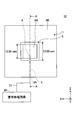
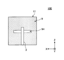
- FIG. 1 is a plan view of the antenna device 10 according to the embodiment.
- the antenna device 10 has a square shape in a plan view from the surface side (Y-axis positive side). Further, as shown in FIG. 1, a thin-film conductor layer 11 made of a conductive material is formed on the surface of the antenna device 10 over the entire surface. Twice
- the antenna device 10 is installed on a vertical installation surface (for example, an outer peripheral surface of a vertically erected pillar). Therefore, in the present embodiment, the vertical side direction (Z-axis direction) of the antenna device 10 is the vertical direction and the vertical direction, and the horizontal side direction (X-axis direction) of the antenna device 10 is the horizontal direction and the left-right direction. Further, in the present embodiment, the direction perpendicular to the surface of the antenna device 10 (that is, the direction orthogonal to the XZ plane) is the Y-axis direction. Further, in the present embodiment, the positive side of the Y-axis of the antenna device 10 is the front side, and the negative side of the Y-axis of the antenna device 10 is the back side. Twice
- a slit-shaped antenna element 5 having a band shape and a square shape is provided at the central portion of the conductor layer 11 of the antenna device 10.
- the antenna element 5 is a so-called slot loop antenna.
- the antenna element 5 is formed by cutting out a part of the conductor layer 11.
- the antenna element 5 is used for transmitting and receiving radio waves in a predetermined frequency band.
- the antenna element 5 is used for transmitting and receiving radio waves in a frequency band less than 6 GHz (for example, 3.7 GHz band or 4.5 GHz band) called "Sub6" used in 5G (5th generation mobile communication system).
- 6 GHz for example, 3.7 GHz band or 4.5 GHz band
- Sub6 used in 5G (5th generation mobile communication system.
- the applicable frequencies are not limited to these.
- the antenna element 5 has a square shape with the vertical side in the vertical direction and the horizontal side in the horizontal direction in a plan view from the front side (Y-axis positive side).
- the inner portion of the antenna element 5 functions as a ground plate 9A
- the outer portion of the antenna element 5 functions as a ground plate 9B. Twice
- the antenna device 10 is provided with a thin-film and band-shaped feeder line 3 made of a conductive material on the back side (Y-axis negative side) of the conductor layer 11.
- the feeder line 3 extends linearly from the center of the lower edge portion of the antenna device 10 in the horizontal direction (X-axis direction) to the upper side (Z-axis positive direction).
- the upper end of the feeder line 3 is connected to the vicinity of the lower edge of the ground plate 9A by the via 4.
- the feeder line 3 is separated from the lower edge of the ground plate 9A by about 1/4 ⁇ g (however, ⁇ g is the length of one wavelength of electrical length including the influence of the dielectric constant of the flexible substrate 12).
- the signal processing circuit 20 is connected to the connection point 3A provided at the lower end of the power supply line 3 via the connection line 21.
- the signal processing circuit 20 includes, for example, an AMP (Amplifier), a switch, a mixer, a DAC (Digital to Analog Converter), an ADC (Analog to Digital Converter), and the like. Twice
- the antenna device 10 is supplied with a signal from the signal processing circuit 20 to the ground plate 9A via the connecting line 21 and the feeding line 3, so that the radio wave (vertical polarization) in a predetermined frequency band for carrying the signal is transmitted. Waves) can be emitted from the antenna element 5.
- the signal processing circuit 20 may be provided outside the antenna device 10 or may be provided on the antenna device 10 (for example, the surface of the flexible substrate 12). Twice
- the length of one side of the square formed by the antenna element 5 is set to "15.00 mm" which is a quarter wavelength of a predetermined frequency
- the length of one side of the square formed by the ground plate 9A is set to "15.00 mm”.
- the length is "12.00 mm”. That is, the bandwidth of the antenna element 5 is "1.50 mm”. Twice
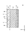
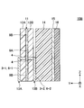
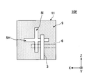
- FIG. 2 is a cross-sectional view taken along the line AA of the antenna device 10 according to the embodiment.
- the antenna device 10 includes a conductor layer 11, a flexible substrate 12, a wiring layer 13, a dielectric 14, a reflector 15, and a flexible substrate 16 in this order from the surface side (Y-axis positive side).
- the antenna device 10 has a multi-layer structure formed by superimposing these plurality of constituent members on each other.
- the antenna device 10 is not limited to the cross-sectional configuration shown in FIG.
- the wiring layer 13 is formed on the front surface of the flexible substrate 12 (the surface on the positive side of the Y axis), and the conductor layer 11 is the back surface (Y) of the flexible substrate 12. It may be formed on the surface on the negative side of the shaft). Further, for example, the reflector 15 may be formed on the back surface (the surface on the negative side of the Y axis) of the flexible substrate 16. Further, the reflector 15 may be provided at least on the back side (Y-axis negative side) of the dielectric 14, for example, the reflector 15 is formed on the back surface (Y-axis negative side) of the dielectric 14. May be done. In this case, the antenna device 10 does not have to have the flexible substrate 16. Twice
- the conductor layer 11 is formed on the surface of the flexible substrate 12 (the surface on the positive side of the Y-axis).
- the conductor layer 11 is thin and has conductivity.
- the conductor layer 11 is formed by using a conductive material such as copper.
- the thickness of the conductor layer 11 is 1 nm to 32 ⁇ m.
- a band-shaped antenna element 5 is formed in a square shape on the conductor layer 11.
- the antenna element 5 is formed by partially cutting out a part of the conductor layer 11.
- a square ground plate 9A is formed in the region surrounded by the antenna element 5.
- the conductor layer 11 is formed on the entire surface of the flexible substrate 12. That is, in the example shown in FIG. 1, the conductor layer 11 has a square shape like the flexible substrate 12 in a plan view. Twice
- the flexible substrate 12 is a flexible, resin-made, thin film-like member.
- the flexible substrate 12 includes fluorine, COP (CycloOlefin Polymer), PET (Polyethylene terephthalate), PEN (polyethylene naphthalate), polyimide, Peek (polyetheretherketone), LCP (Liquid Crystal Polymer), and other composite materials. , Formed using a flexible resin material.
- the thickness of the flexible substrate 16 is 1 ⁇ m to 300 ⁇ m.
- the flexible substrate 12 is provided with a via 4 that penetrates the flexible substrate 12 in the vertical direction. Twice
- the wiring layer 13 is formed on the back surface (the surface on the negative side of the Y axis) of the flexible substrate 12.
- the wiring layer 13 is provided with a thin-film and band-shaped feeder line 3 extending linearly in the vertical direction (Z-axis direction).
- the upper end of the feeder line 3 is connected so as to be orthogonal to the lower side of the ground plate 9A via a via 4 provided on the flexible substrate 12.
- the antenna element 5 can radiate vertically polarized waves. Twice
- the dielectric 14 is a plate-shaped member that is provided so as to be overlapped on the back side of the flexible substrate 12 and has flexibility and can be bent.
- the dielectric 14 is formed by using an elastic dielectric material (for example, sponge, rubber, urethane, etc.).
- the dielectric 14 has a thickness that enables a predetermined bandwidth to be secured in a predetermined frequency band.
- the suitable thickness of the dielectric 14 can be determined by simulation or the like.
- the dielectric 14 is adhered to the back surface (the surface on the negative side of the Y axis) of the flexible substrate 12 by any adhesive means (for example, an adhesive, double-sided tape, etc.).
- the shape and size of the dielectric 14 are the same as the shape and size of the flexible substrate 12, but the shape and size are not limited to this.
- the dielectric 14 may have a size larger than that of the flexible substrate 12, and may have a shape different from that of the flexible substrate 12 (that is, a shape other than a square shape).
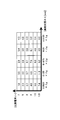
- FIGS. 17 and 18 show an example of a bandwidth based on a combination of the thickness of the dielectric 14 and the relative permittivity in the antenna device 10 according to the embodiment (the antenna device 10 having the configurations shown in FIGS. 1 and 2). It is a figure. Note that FIG. 17 shows an example of a bandwidth in which VSWR is less than 1.5. Further, FIG. 18 shows an example of a bandwidth in which VSWR is less than 2.0. Twice
- the bandwidth of the antenna device 10 can be determined based on the combination of the thickness of the dielectric 14 and the relative permittivity. Therefore, in order to make the bandwidth of the antenna device 10 suitable (that is, a sufficiently wide band width), the list shown in FIGS. 17 and 18 is obtained in advance by simulation or the like, and the list is actually obtained based on the list. It is preferable to determine the thickness and relative permittivity of the dielectric 14 to be used. The relative permittivity of the dielectric 14 can be changed, for example, by adjusting or changing the material. Twice
- the bandwidth in which VSWR is less than 1.5 is preferably 2% or more, more preferably 3% or more, still more preferably 5% or more.
- the combination of the thickness of the dielectric 14 and the relative permittivity at which the bandwidth is 2% or more, 3% or more, or 5% or more may be determined from the list shown in FIG. Twice
- the bandwidth in which VSWR is less than 2.0 is preferably 3.5% or more, more preferably 7% or more, and further preferably 10.5% or more.
- the combination of the thickness of the dielectric 14 and the relative permittivity at which the bandwidth is 3.5% or more, 7% or more, or 10.5% or more may be determined from the list shown in FIG. Twice
- the antenna device 10 according to the embodiment is configured to be bendable and has a dielectric 14, so that the antenna device 10 is generally bendable as compared with the conventional bendable antenna device. It is possible to obtain a sufficiently wide band width. Further, it has been confirmed that even when the antenna device 10 according to the embodiment is used in a curved state, the bandwidth hardly changes as compared with the case where the antenna device 10 is used in a flat state. Twice
- the reflector 15 is formed over the entire surface of the flexible substrate 16 (the surface on the positive side of the Y-axis).
- the reflector 15 is thin and conductive.
- the reflector 15 is formed by using a conductive material such as copper. Further, for example, the thickness of the reflector 15 is 1 nm to 32 ⁇ m.
- the reflector 15 is provided to reflect the radiation from the antenna element 5 to the back side (Y-axis negative side) of the antenna device 10 to the radio waves. Twice
- the flexible substrate 16 is provided so as to be overlapped on the back surface (the surface on the negative side of the Y axis) of the dielectric 14.
- the flexible substrate 16 is a flexible, resin-made, thin film-like member.
- the flexible substrate 16 is formed by using the same material as the flexible substrate 12.
- the present invention is not limited to this, and at least one of the material and the thickness of the flexible substrate 16 may be different from that of the flexible substrate 12.
- the flexible substrate 16 has a reflective plate 15 formed on the front surface (the surface on the positive side of the Y-axis), and the back surface of the dielectric 14 (for example, an adhesive, double-sided tape, etc.) is used by any adhesive means (for example, an adhesive, double-sided tape, etc.). It is adhered to the negative side of the Y-axis). Twice
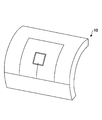
- FIG. 3 is a diagram showing an installation example of the pillar 70 of the antenna device 10 according to the embodiment on the outer peripheral surface 70A.
- the antenna device 10 is generally bendable because the dielectric 14 and the flexible substrates 12 and 16 are bendable. Therefore, as shown in FIG. 3, the antenna device 10 can be installed on the outer peripheral surface 70A in a state of being curved along the outer peripheral surface 70A of the pillar 70.
- the antenna device 10 can be installed on the outer peripheral surface 70A of a pillar 70 such as a traffic light, a street light, or a utility pole, but is not limited thereto.
- the antenna device 10 can be fixed to the outer peripheral surface 70A of the pillar 70 by an arbitrary fixing method (for example, adhesive, double-sided tape, etc.). Twice
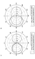
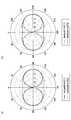
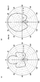
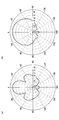
- FIG. 5A shows the directivity of the ZY plane in the 4.85 GHz band of the antenna device 10.
- FIG. 5B shows the directivity of the XY plane in the 4.85 GHz band of the antenna device 10. Twice
- the solid line represents the directivity when the reflector 15 is provided on the antenna device 10
- the broken line indicates the directivity when the reflector 15 is not provided on the antenna device 10. It represents directivity. Twice
- the antenna device 10 radiates vertically polarized waves having a sufficiently high gain with respect to the surface direction (Y-axis positive direction) of the antenna device 10 by the antenna element 5. can. Twice
- the antenna device 10 according to the embodiment is provided with the reflecting plate 15 so that the antenna device 10 is oriented in the back surface direction (Y-axis negative direction).
- Vertically polarized waves can be reflected in the surface direction (Y-axis positive direction) of the antenna device 10. Therefore, the antenna device 10 according to the embodiment can enhance the radio wave intensity of vertically polarized waves with respect to the surface direction (Y-axis positive direction) of the antenna device 10. Twice
- the antenna device 10 according to the embodiment can suppress the influence of the outer peripheral surface 70A, which is the installation target, on the radio waves radiated from the antenna element 5 by providing the reflector 15. That is, the antenna device 10 according to the embodiment can be installed on various outer peripheral surfaces 70A regardless of the material of the outer peripheral surface 70A. Twice
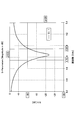
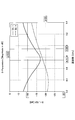
- FIG. 6 is a graph showing the antenna characteristics (S11) of the antenna device 10 according to the embodiment.
- the antenna device 10 according to the embodiment is provided with a dielectric 14 having a certain thickness (15 mm in this test) and a reflector 15, thereby providing a predetermined frequency band (4).
- the reflectance coefficient (S11) can be suppressed to "-10 dB" or less (corresponding to VSWR ⁇ 2). That is, the antenna device 10 according to the embodiment can obtain a wide bandwidth (200 MHz) in a predetermined frequency band (4.75 to 4.95 GHz). Twice
- FIG. 19 is an external perspective view showing the first use state of the antenna device 10 according to the embodiment.
- FIG. 20 is a graph showing antenna characteristics (VSWR value) in the first usage state of the antenna device 10 according to the embodiment.
- the antenna device 10 according to the embodiment can be used in a flat state as a first usage state. This first usage state is effective when the antenna device 10 is installed on a flat installation target surface.
- the antenna device 10 according to the embodiment can obtain a wide bandwidth with a center frequency of 3.8 GHz in the first use state, and in particular, VSWR is less than 1.5. It was confirmed that a sufficiently wide band width of "4.1%" can be obtained as the bandwidth. Twice
- FIG. 21 is an external perspective view showing a second use state of the antenna device 10 according to the embodiment.
- FIG. 22 is a graph showing the antenna characteristics (VSWR value) in the second usage state of the antenna device 10 according to the embodiment.
- the antenna device 10 according to the embodiment can be used in a curved state curved along the horizontal direction as a second usage state. This second usage state is effective when the antenna device 10 is installed on an installation target surface (for example, an outer peripheral surface of a columnar column) curved along the horizontal direction.
- an installation target surface for example, an outer peripheral surface of a columnar column
- the antenna device 10 can obtain a wide bandwidth having a center frequency of 3.8 GHz in the second use state, and in particular, VSWR is less than 1.5. It was confirmed that a sufficiently wide band width of "2.5%" can be obtained as the bandwidth. Twice
- FIG. 23 is an external perspective view showing a third use state of the antenna device 10 according to the embodiment.
- FIG. 24 is a graph showing the antenna characteristics (VSWR value) in the third usage state of the antenna device 10 according to the embodiment.
- the antenna device 10 according to the embodiment can be used in a curved state curved along the vertical direction as a third usage state. This third usage state is effective when the antenna device 10 is installed on an installation target surface curved along the vertical direction.
- the antenna device 10 according to the embodiment can obtain a wide bandwidth with 3.8 GHz as the center frequency in the third use state, and in particular, VSWR is less than 1.5. It was confirmed that a sufficiently wide band width of "3.9%" can be obtained as the bandwidth. Twice
- the thickness of the dielectric 14 is set to "0.1875 * ⁇ g", and the dielectric is dielectric.
- the relative permittivity of the body 14 is set to "2". Twice
- the antenna device 10 has the configurations shown in FIGS. 1 and 2, so that a sufficient wide band width can be obtained regardless of whether the antenna device 10 is used in a flat state or a curved state. It was confirmed that Twice
- FIG. 7 is a plan view of the antenna device 10A according to the first modification.
- the antenna device 10A shown in FIG. 7 is an antenna shown in FIG. 1 in that a thin-film and band-shaped feeder line 6 made of a conductive material is further provided on the wiring layer 13 on the back side (Y-axis negative side) of the conductor layer 11. Different from device 10.
- the feeder line 6 extends linearly from the center of the left edge of the antenna device 10 to the right (in the negative direction of the X-axis).
- the right end of the feeder line 6 is connected by the via 4 to the vicinity of the left edge of the ground plate 9A.
- the signal processing circuit 20 is connected to the connection point 6A provided at the left end of the power supply line 6 via the connection line 22. Twice
- the antenna device 10A according to the first modification can radiate vertically polarized waves and horizontally polarized waves from the antenna element 5.
- the antenna device 10A according to the first modification supplies a signal from the signal processing circuit 20 to the ground plate 9A via the connection line 21 and the feeder line 3 (first feeder line).
- the antenna element 5 can emit vertically polarized waves in a predetermined frequency band.
- the antenna device 10A according to the first modification is an antenna element by supplying a signal from the signal processing circuit 20 to the ground plate 9A via the connecting line 22 and the feeding line 6 (second feeding line). It can radiate horizontally polarized waves in a predetermined frequency band from 5. Twice
- FIG. 8 is a diagram showing the directivity of the antenna device 10A according to the first modification.
- FIG. 8A shows the antenna characteristics of the ZY plane in the 4.85 GHz band of the antenna device 10A according to the first modification.
- FIG. 8B shows the antenna characteristics of the XY plane in the 4.85 GHz band of the antenna device 10A according to the first modification.
- the solid line represents the antenna characteristics of the vertically polarized YZ plane radiated from the antenna element 5, and the broken line represents the antenna characteristics of the vertically polarized YX plane radiated from the antenna element 5.
- the solid line represents the antenna characteristics of the horizontally polarized YZ plane radiated from the antenna element 5
- the broken line represents the antenna characteristics of the horizontally polarized YX plane radiated from the antenna element 5. .. Twice
- the antenna device 10A according to the first modification is sufficiently higher than the surface direction (Y-axis positive direction) of the antenna device 10A by the antenna element 5. It can emit each of vertically polarized waves and horizontally polarized waves having a gain. Twice
- the antenna device 10A according to the first modification is provided with a reflecting plate 15 so that the antenna device 10A is vertically polarized and horizontally polarized with respect to the back surface direction (Y-axis negative direction). By reflecting the radiation of, the radio wave in the surface direction (Y-axis positive direction) can be strengthened. Twice
- FIG. 9 is a graph showing the antenna characteristics (S11, S21) of the antenna device 10A according to the first modification.
- the solid line represents the reflection coefficient (S11) of each of the vertically polarized light and the horizontally polarized light by the antenna device 10A
- the broken line represents the transmission coefficient of each of the vertically polarized light and the horizontally polarized light by the antenna device 10A. Represents (S21). Twice
- the antenna device 10A according to the first modification has a predetermined frequency band due to the provision of the dielectric 14 having a certain thickness (15 mm in this test) and the reflecting plate 15.
- the reflectance coefficients (S11) of each of the vertically polarized wave and the horizontally polarized wave can be suppressed to "-10 dB" or less (corresponding to VSWR ⁇ 2). Twice
- the antenna device 10A according to the first modification has a transmission coefficient (S21) of vertically polarized light and horizontally polarized light in a predetermined frequency band (4.75 to 4.95 GHz). Can be suppressed to "-15 dB" or less. Twice
- the antenna device 10 can obtain a wide bandwidth (for example, 200 MHz or more) in a predetermined frequency band (4.75 to 4.95 GHz). Twice
- FIG. 10 is a plan view of the antenna device 10B according to the second modification. Twice
- the antenna device 10B shown in FIG. 10 includes a plurality of antenna elements 5 arranged side by side in a matrix arranged in each of the horizontal direction (X-axis direction) and the vertical direction (Z-axis direction) on the conductor layer 11.
- the antenna device 10B eight antenna elements 5 are arranged side by side in each of the horizontal direction (X-axis direction) and the vertical direction (Z-axis direction). That is, the antenna device 10B has 64 antenna elements 5 arranged in an 8 ⁇ 8 matrix on the conductor layer 11. Twice
- the plurality of antenna elements 5 and the feeder lines 3 and 6 in the lower four rows are the antenna elements 5 and the feeder lines 3 and 6 of the antenna device 10A shown in FIG.
- the configuration is rotated counterclockwise by 45 °.
- the feeder line 3 is connected at right angles to the lower right hypotenuse of the ground plate 9A inside the antenna element 5, and the feeder line 6 is connected to the ground plate 9A. It is connected at right angles to the lower left hypotenuse. Twice
- the plurality of antenna elements 5 and the feeder lines 3 and 6 in the upper four rows are compared with the antenna elements 5 and the feeder lines 3 and 6 in the lower four rows. It has an upside down configuration.
- the feeder line 3 is connected at right angles to the upper right hypotenuse of the ground plate 9A
- the feeder line 6 is connected at right angles to the upper left hypotenuse of the ground plate 9A. Has been done. Twice
- the antenna device 10B configured in this way radiates two types of radio waves whose polarization directions differ from each other by 90 ° by supplying electric power to the feeder line 3 or the feeder line 6 for each of the plurality of antenna elements 5. be able to. Twice
- FIG. 11 is a diagram showing a connection example of the feeder lines 3 and 6 in the antenna device 10B according to the second modification.
- FIG. 11 illustrates the four lower antenna elements 5 arranged in the vertical direction in the antenna device 10B.
- the antenna device 10B includes two feeder lines 3-1 and 3-2 and two feeder lines 6-1 and 6-2 for the four antenna elements 5. ..
- Feed lines 3-1 and 6-1 are connected to each of the two lower antenna elements 5.
- Feed lines 3-2 and 6-2 are connected to each of the two upper antenna elements 5.
- Each of the feeder lines 3-1, 3-2, 6-1 and 6-2 is connected to the signal processing circuit 20. Twice
- the antenna device 10B configured in this way supplies power from the signal processing circuit 20 to the feeder line 3-1 or the feeder line 6-1 to supply power to the lower two antennas of the four antenna elements 5. Two types of radio waves having different polarization directions by 90 ° can be emitted from the element 5. Twice
- the antenna device 10B supplies electric power from the signal processing circuit 20 to the feeder line 3-2 or the feeder line 6-2, so that the two antenna elements 5 on the upper side of the four antenna elements 5 supply each other. It is possible to emit two types of radio waves with different polarization directions by 90 °. Twice
- the polarization directions differ from each other by 90 ° in each of a plurality of directions (maximum 8 directions) centered on the pillar 70. It can emit each of the types of radio waves. In this case, the antenna device 10B can more reliably reach the radio waves in each of the plurality of directions (up to eight directions) around the pillar 70. Twice
- the antenna device 10B can individually drive each of the 64 antenna elements 5 as needed, that is, can radiate radio waves only in a specific one or a plurality of directions. .. Further, the antenna device 10B can radiate radio waves simultaneously or with a time lag in a plurality of specific directions. Further, the antenna device 10B can transmit a plurality of types of signals different from each other in a specific plurality of directions at the same time or with a time lag. For example, the antenna device 10B can also be used for MIMO (multiple-input and multiple-output), beamforming, and the like. Twice
- MIMO multiple-input and multiple-output
- FIG. 12 is a diagram showing a cross-sectional configuration of the antenna device 10B according to the second modification.
- the first wiring layer 13A, the first flexible substrate 12A, the conductor layer 11, and the second are in order from the surface side (Y-axis positive side). It includes a flexible substrate 12B, a second wiring layer 13B, a dielectric 14, a reflector 15, and a flexible substrate 16.
- the reflector 15 may be provided at least on the back side (Y-axis negative side) of the dielectric 14, for example, the reflector 15 is the back surface (Y-axis negative side) of the dielectric 14. It may be formed on the side surface). In this case, the antenna device 10B does not have to have the flexible substrate 16. Twice
- the antenna device 10B in the antenna device 10B according to the second modification, two flexible substrates 12A and 12B are provided so as to overlap each other.
- the antenna device 10B is provided with a conductor layer 11 between the two flexible substrates 12A and 12B.
- the first wiring layer 13A is provided on the front surface of the first flexible substrate 12A
- the second wiring layer 13B is provided on the back surface of the second flexible substrate 12B. .. Twice
- the first wiring layer 13A is provided with the feeder lines 3-1 and 6-1 shown in FIG.
- the feeder lines 3-1 and 6-1 are connected to the ground plate 9A provided on the conductor layer 11 via the via 4 penetrating the first flexible substrate 12A. Twice
- the feed line 3-2, 6-2 shown in FIG. 11 is provided on the second wiring layer 13B.
- the feeder lines 3-2 and 6-2 are connected to the ground plate 9A provided on the conductor layer 11 via the via 4 penetrating the second flexible substrate 12B. Twice
- the antenna device 10B according to the second modification is provided with the first wiring layer 13A and the second wiring layer 13B, so that a plurality of feeder lines can be connected to the first wiring layer 13A and the second wiring layer 13A. It can be distributed to layer 13B.
- the antenna device 10B according to the second modification can suppress the number of wires in each of the wiring layers 13A and 13B, and therefore can increase the degree of freedom of wiring in each of the wiring layers 13A and 13B. Twice
- FIG. 13 is a plan view of the antenna device 10C according to the third modification.
- the antenna device 10C shown in FIG. 13 includes a dipole antenna ANT1, a dipole antenna ANT2, a feeder line 3, and a ground plate 9. Twice
- the ground plate 9 has a vertically long rectangular base portion 9a, a branch portion 9b that branches from the left edge portion of the base portion 9a to the left, and a branch portion that branches from the right edge portion of the base portion 9a to the right. It has a part 9c. Twice
- the feeder line 3 is provided above the ground plate 9 and overlapped with the ground plate 9.
- the feeding line 3 has a straight portion 3a extending linearly upward from the lower end portion of the antenna device 10C and a straight portion 3a to the left from the upper end portion of the straight portion 3a in the central portion of the antenna device 10C in the horizontal direction (X-axis direction). It has a branch portion 3b that branches to the right side and a branch portion 3c that branches to the right from the upper end portion of the straight line portion 3a. Twice
- the dipole antenna ANT1 includes an antenna element 5A extending linearly upward and an antenna element 5B extending linearly downward on the left side of the ground plate 9.
- the lower end of the antenna element 5A is connected to the left end of the branch portion 9b of the ground plate 9.
- the upper end of the antenna element 5B is connected to the left end of the branch 3b of the feeder line 3. Twice
- the dipole antenna ANT2 includes an antenna element 5C extending linearly upward and an antenna element 5D extending linearly downward on the right side of the ground plate 9.
- the lower end of the antenna element 5C is connected to the right end of the branch portion 9c of the ground plate 9.
- the upper end of the antenna element 5D is connected to the right end of the branch 3c of the feeder line 3. Twice
- the ground plate 9, the antenna element 5A, and the antenna element 5C are formed on the back surface of the flexible substrate 12 (see FIG. 12). Further, in the antenna device 10C, the feeder line 3, the antenna element 5B, and the antenna element 5D are formed on the surface of the flexible substrate 12. Twice
- the antenna device 10C configured in this way emits vertically polarized waves in a predetermined frequency band from each of the dipole antennas ANT1 and ANT2 by supplying electric power from the feeder line 3 to each of the antenna elements 5B and 5D. be able to. Twice
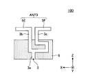
- FIG. 14 is a plan view of the antenna device 10D according to the fourth modification.
- the antenna device 10D shown in FIG. 14 includes a dipole antenna ANT3, a feeder line 3, and a ground plate 9.
- the ground plate 9 has a vertically long rectangular shape.
- the dipole antenna ANT3 and the feeder line 3 are provided above the ground plate 9. Twice
- the feeder line 3 has a straight portion 3a extending linearly in the vertical direction, a branch portion 3b branching to the left from the upper end portion of the straight portion 3a, and a branch portion branching to the right from the upper end portion of the straight portion 3a. It has 3c and. Twice
- the dipole antenna ANT3 has an antenna element 5E extending linearly to the left from the upper end of the branch portion 3b of the feeder line 3 above the ground plate 9, and a branch portion 3c of the feeder line 3 to the right from the upper end portion. It is provided with an antenna element 5F extending linearly. Twice
- the ground plate 9 is formed on the back surface of the flexible substrate 12 (see FIG. 12). Further, in the antenna device 10D, the feeder line 3, the antenna element 5E, and the antenna element 5F are formed on the surface of the flexible substrate 12. Twice
- the antenna device 10D configured in this way can radiate horizontally polarized waves in a predetermined frequency band from the dipole antenna ANT3 by supplying electric power to each of the antenna elements 5E and 5F from the feeder line 3. Twice
- FIG. 15 is a plan view of the antenna device 10E according to the fifth modification.
- the antenna device 10E shown in FIG. 15 includes an antenna element 5H and a feeder line 3. Twice
- a band-shaped and slit-shaped antenna element extending linearly in the horizontal direction (X-axis direction) at the center of the conductor layer 11 of the antenna device 10E in the vertical direction (Z-axis direction). 5H is provided.
- the antenna element 5H is a so-called slot antenna.
- the antenna element 5H is formed by cutting out a part of the conductor layer 11. In the conductor layer 11 of the antenna device 10E, the outer portion of the antenna element 5H functions as the ground plate 9. Twice
- the feeder line 3 extends linearly upward from the lower end portion of the antenna device 10E at the central portion of the antenna device 10E in the horizontal direction (X-axis direction).
- the upper end of the feeder line 3 is about 1/4 ⁇ g away from the upper edge of the antenna element 5H on the ground plate 9 (where ⁇ g is the length of one wavelength of electricity including the influence of the dielectric constant of the flexible substrate 12). It is open at a location and is non-contact and electrically connected to the antenna element 5H by electromagnetic coupling. As a result, the antenna element 5H can radiate vertically polarized waves. Twice
- the antenna device 10E configured in this way can radiate vertically polarized waves in a predetermined frequency band from the antenna element 5H by supplying electric power from the feeder line 3 to the ground plate 9. Twice
- FIG. 16 is a plan view of the antenna device 10F according to the sixth modification.
- the antenna device 10F shown in FIG. 16 has a configuration in which the antenna element 5I and the feeding line 6 are further provided with respect to the antenna device 10E shown in FIG. Twice
- the antenna element 5I has a band shape and a slit shape like the antenna element 5H.
- the antenna element 5I is provided in the conductor layer 11 of the antenna device 10F so as to extend linearly in the vertical direction (Z-axis direction) at the central portion in the horizontal direction (X-axis direction).
- the antenna element 5I is orthogonal to the antenna element 5H. Twice
- the feeder line 3 is provided on the front side of the conductor layer 11 so as to extend linearly upward from the lower end portion of the antenna device 10E.
- the upper end of the feeder line 3 is about 1/4 ⁇ g away from the upper edge of the antenna element 5H on the ground plate 9 (where ⁇ g is the length of one wavelength of electricity including the influence of the dielectric constant of the flexible substrate 12). It is open at a location and is non-contact and electrically connected to the antenna element 5H by electromagnetic coupling. As a result, the antenna element 5H can radiate vertically polarized waves. Twice
- the feeder line 6 is provided on the back side of the conductor layer 11 so as to extend linearly from the right end portion of the antenna device 10E to the left.
- the left end of the feeder 6 is about 1/4 ⁇ g away from the left edge of the antenna element 5I on the ground plate 9 (where ⁇ g is the length of one wavelength of electricity including the influence of the dielectric constant of the flexible substrate 12). It is open in place and is non-contact and electrically connected to the antenna element 5I by electromagnetic coupling. As a result, the antenna element 5I can radiate horizontally polarized waves. Twice
- the conductor layer 11 is provided between the two flexible substrates 12A and 12B, similarly to the antenna device 10B shown in FIG.
- the feed line 3 is provided on the surface of the first flexible substrate 12A, and is non-contactly and electrically connected to the antenna element 5H by electromagnetic coupling.
- the feed line 6 is provided on the back surface of the second flexible substrate 12B, and is non-contactly and electrically connected to the antenna element 5I by electromagnetic coupling. Twice
- the antenna device 10F configured in this way can radiate vertically polarized waves in a predetermined frequency band from the antenna element 5H by supplying electric power from the feeder line 3 to the ground plate 9. Twice
- the antenna device 10F can radiate horizontally polarized waves in a predetermined frequency band from the antenna element 5I by supplying electric power from the feeder line 6 to the ground plate 9. Twice
- each of the antenna devices 10B to 10F described above has a dielectric 14 having a constant thickness and a reflector 15. Therefore, all of the antenna devices 10B to 10F can be installed along the curved installation surface, a wide bandwidth in a predetermined frequency band can be obtained, and the radiation of radio waves in the back surface direction is reflected. As a result, the radiation toward the surface can be strengthened. Twice
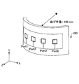
- FIG. 25 is an external perspective view showing a planar state of the antenna device 10G according to the seventh modification.
- the antenna device 10G according to the seventh modification has a horizontally long rectangular shape in a plan view from the surface side (Z-axis positive side).
- the antenna device 10G according to the seventh modification includes four antenna elements 5 arranged side by side in the X-axis direction on the conductor layer 11.
- Each antenna element 5 is similar to the antenna element 5 shown in FIGS. 1 and 2, that is, has a band shape and a square shape.
- the ground plate 9A inside each antenna element 5 is connected to the signal processing circuit 20 via the feeder line 3 and the connection line 21.
- antenna device 10G according to the seventh modification are the same as those of the antenna device 10 shown in FIGS. 1 and 2.
- the arrangement interval between two adjacent antenna elements is 0.5 ⁇ o.
- the thickness of the dielectric 14 is set to "0.1875 * ⁇ o"
- the relative permittivity of the dielectric 14 is set to "2".
- the antenna device 10G according to the seventh modification can be used in a plane state parallel to the XY plane. Twice
- FIG. 26 is a diagram showing the directivity of the antenna device 10G (planar state shown in FIG. 25) according to the seventh modification.
- FIG. 26A shows the antenna characteristics of the ZX plane in a predetermined frequency band of the antenna device 10G according to the seventh modification.
- FIG. 26B shows the antenna characteristics of the YZ plane in a predetermined frequency band of the antenna device 10G according to the seventh modification.
- the antenna device 10 according to the embodiment is a radio wave having a sufficiently high gain (12.4 dBi) in a specific direction even when a plurality of antenna elements 5 are arranged in an array. It was confirmed that it can radiate. Twice
- FIG. 27 is an external perspective view showing a curved state of the antenna device 10G according to the seventh modification.
- the antenna device 10G according to the seventh modification can be used in a curved state curved with respect to the XY surface.
- the radius of curvature of the antenna device 10G is 100 mm. Twice
- FIG. 28 is a diagram showing the directivity of the antenna device 10G (curved state shown in FIG. 27) according to the seventh modification.
- FIG. 28A shows the antenna characteristics of the ZX plane in a predetermined frequency band of the antenna device 10G according to the seventh modification.
- FIG. 28B shows the antenna characteristics of the YZ plane in a predetermined frequency band of the antenna device 10G according to the seventh modification.
- the antenna device 10 according to the embodiment even when a plurality of antenna elements 5 are arranged in an array and in a curved state, there is no significant change from the case where the antenna device 10 is used in a flat state. It was confirmed that radio waves having a sufficiently high gain (11.1 dBi) can be emitted in a specific direction. Twice
- the configuration shown in the above-described embodiment shows an example of the contents of the present disclosure, can be combined with another known technique, and is one of the configurations as long as it does not deviate from the gist of the present disclosure. It is also possible to omit or change the part.
Abstract
This antenna device is provided with: a flexible substrate; an antenna element provided on a front surface or back surface of the flexible substrate; a thin film of feed line provided on the front surface or back surface of the flexible substrate to feed the antenna element; a plate-shaped dielectric body superposed on the back side of the flexible substrate, the dielectric body having flexibility and capable of being bent; and a reflective plate provided on the back side of the dielectric body.
Description
本開示は、アンテナ装置に関する。
The present disclosure relates to an antenna device.
近年、4G LTEから5G(sub6)への移行など、マイクロ波やミリ波の周波数帯を使用する高速・大容量の無線通信システムを利用するサービスが拡がる動きがある。このような周波数帯で使用されるアンテナとして、一般的にはCCLと呼ばれるリジット基板を用いたパッチアンテナが知られている。
In recent years, there has been a movement to expand services using high-speed, large-capacity wireless communication systems that use microwave and millimeter-wave frequency bands, such as the shift from 4G LTE to 5G (sub6). As an antenna used in such a frequency band, a patch antenna using a rigid substrate generally called CCL is known. Twice
特許文献1のアンテナ装置によれば、領域によって厚みの異なるフレキシブル基板を用い、LTCC基板などのリジッドな基板とフレキシブル基板を接続する場合と比べて構造を簡素化しつつ、複数の方向にビームを放射することが可能となる。
According to the antenna device of Patent Document 1, a flexible substrate having a different thickness depending on a region is used, and a beam is emitted in a plurality of directions while simplifying a structure as compared with a case where a rigid substrate such as an LTCC substrate and a flexible substrate are connected. It becomes possible to do.
ところで、本発明の発明者らが実施した試験によれば、「Sub6」と呼ばれる6GHz未満の周波数帯(例えば3.7GHz帯や4.5GHz帯)に用いられるパッチアンテナ等のアンテナ装置において、所定の周波数帯における広い帯域幅を確保するためには、例えばガラス基板の場合は板厚を6mm以上とする等、パッチアンテナを構成する基板に十分な厚みを有することが好ましいことが判明した。
By the way, according to the test carried out by the inventors of the present invention, a predetermined antenna device such as a patch antenna used in a frequency band of less than 6 GHz (for example, 3.7 GHz band or 4.5 GHz band) called "Sub6". In order to secure a wide bandwidth in the frequency band of, it has been found that it is preferable that the substrate constituting the patch antenna has a sufficient thickness, for example, in the case of a glass substrate, the plate thickness is 6 mm or more. Twice
しかしながら従来技術では、ガラス基板や樹脂基板の板厚が厚くなるにつれて、アンテナ装置を湾曲させることが困難になり、したがって、アンテナ装置を曲面状の設置面(例えば、柱状の設置物の外周面)に設置することが困難になる。
However, in the prior art, as the thickness of the glass substrate or resin substrate increases, it becomes difficult to bend the antenna device, and therefore, the antenna device is mounted on a curved installation surface (for example, an outer peripheral surface of a columnar installation object). It becomes difficult to install in. Twice
本開示は、上記に鑑みてなされたものであって、曲面状の設置面に沿って設置可能であり、所定の周波数帯における広い帯域幅を得ることができ、且つ、裏面方向に対する電波の放射を反射して一方向に強く電波を放射できるアンテナ装置を提供することを目的とする。
The present disclosure has been made in view of the above, can be installed along a curved installation surface, can obtain a wide bandwidth in a predetermined frequency band, and emits radio waves in the back surface direction. It is an object of the present invention to provide an antenna device capable of reflecting radio waves and radiating radio waves strongly in one direction.
上述した課題を解決し、目的を達成するため、本開示に係るアンテナ装置は、フレキシブル基板と、フレキシブル基板の表面または裏面に設けられたアンテナ素子と、フレキシブル基板の表面または裏面に設けられ、アンテナ素子に給電する薄膜状の給電線と、フレキシブル基板の裏側に重ねて設けられ、柔軟性を有して湾曲可能な板状の誘電体と、誘電体の裏側に設けられた反射板とを備える。
In order to solve the above-mentioned problems and achieve the object, the antenna device according to the present disclosure is provided on a flexible substrate, an antenna element provided on the front surface or the back surface of the flexible substrate, and an antenna provided on the front surface or the back surface of the flexible substrate. It includes a thin-film feeding line that feeds the element, a plate-shaped dielectric that is provided so as to be overlapped on the back side of a flexible substrate and is flexible and bendable, and a reflecting plate that is provided on the back side of the dielectric. ..
本開示のアンテナ装置によれば、曲面状の設置面に沿って設置可能であり、所定の周波数帯における広い帯域幅を得ることができ、且つ、裏面方向に対する電波の放射を反射して一方向に強く電波を放射できるアンテナ装置を提供できる。
According to the antenna device of the present disclosure, it can be installed along a curved installation surface, a wide bandwidth in a predetermined frequency band can be obtained, and the radiation of radio waves to the back surface direction is reflected in one direction. It is possible to provide an antenna device capable of radiating radio waves strongly.
以下、図面を参照して、本開示に係る実施形態について説明する。
Hereinafter, embodiments according to the present disclosure will be described with reference to the drawings. Twice
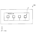
(アンテナ装置10の構成) 図1は、実施形態に係るアンテナ装置10の平面図である。図1に示すように、アンテナ装置10は、表面側(Y軸正側)からの平面視において正方形状を有する。また、図1に示すように、アンテナ装置10の表面には、全域に亘って、導電性素材からなる薄膜状の導体層11が形成されている。
(Structure of Antenna Device 10) FIG. 1 is a plan view of the antenna device 10 according to the embodiment. As shown in FIG. 1, the antenna device 10 has a square shape in a plan view from the surface side (Y-axis positive side). Further, as shown in FIG. 1, a thin-film conductor layer 11 made of a conductive material is formed on the surface of the antenna device 10 over the entire surface. Twice
なお、本実施形態では、アンテナ装置10は、垂直な設置面(例えば、垂直に立設された柱の外周面)に設置される。よって、本実施形態では、アンテナ装置10の縦辺方向(Z軸方向)を垂直方向および上下方向とし、アンテナ装置10の横辺方向(X軸方向)を水平方向および左右方向とする。さらに、本実施形態では、アンテナ装置10の表面に対する垂線方向(すなわち、XZ面と直交する方向)をY軸方向とする。また、本実施形態では、アンテナ装置10のY軸正側を表側とし、アンテナ装置10のY軸負側を裏側とする。
In this embodiment, the antenna device 10 is installed on a vertical installation surface (for example, an outer peripheral surface of a vertically erected pillar). Therefore, in the present embodiment, the vertical side direction (Z-axis direction) of the antenna device 10 is the vertical direction and the vertical direction, and the horizontal side direction (X-axis direction) of the antenna device 10 is the horizontal direction and the left-right direction. Further, in the present embodiment, the direction perpendicular to the surface of the antenna device 10 (that is, the direction orthogonal to the XZ plane) is the Y-axis direction. Further, in the present embodiment, the positive side of the Y-axis of the antenna device 10 is the front side, and the negative side of the Y-axis of the antenna device 10 is the back side. Twice
図1に示す例では、アンテナ装置10の導体層11における中央部には、帯状且つ正方形状を有するスリット状のアンテナ素子5が設けられている。アンテナ素子5は、いわゆるスロットループアンテナである。アンテナ素子5は、導体層11の一部が切り欠かれることによって形成される。アンテナ素子5は、所定の周波数帯の電波の送受信に用いられる。例えば、アンテナ素子5は、5G(第5世代移動通信システム)で使用される、「Sub6」と呼ばれる6GHz未満の周波数帯(例えば3.7GHz帯や4.5GHz帯)の電波の送受信に用いられるが、適用可能な周波数はこれらに限られない。アンテナ素子5は、表側(Y軸正側)からの平面視において、縦辺を垂直方向とし、横辺を水平方向とする正方形状を有する。なお、導体層11において、アンテナ素子5の内側の部分はグラウンド板9Aとして機能し、アンテナ素子5の外側の部分は、グラウンド板9Bとして機能する。
In the example shown in FIG. 1, a slit-shaped antenna element 5 having a band shape and a square shape is provided at the central portion of the conductor layer 11 of the antenna device 10. The antenna element 5 is a so-called slot loop antenna. The antenna element 5 is formed by cutting out a part of the conductor layer 11. The antenna element 5 is used for transmitting and receiving radio waves in a predetermined frequency band. For example, the antenna element 5 is used for transmitting and receiving radio waves in a frequency band less than 6 GHz (for example, 3.7 GHz band or 4.5 GHz band) called "Sub6" used in 5G (5th generation mobile communication system). However, the applicable frequencies are not limited to these. The antenna element 5 has a square shape with the vertical side in the vertical direction and the horizontal side in the horizontal direction in a plan view from the front side (Y-axis positive side). In the conductor layer 11, the inner portion of the antenna element 5 functions as a ground plate 9A, and the outer portion of the antenna element 5 functions as a ground plate 9B. Twice
また、図1に示すように、アンテナ装置10は、導体層11の裏側(Y軸負側)に、導電性素材からなる薄膜状且つ帯状の給電線3を備える。給電線3は、アンテナ装置10の下縁部の水平方向(X軸方)における中央から、上方(Z軸正方向)に直線状に延在する。給電線3の上端部は、ビア4によって、グラウンド板9Aの下縁部の近傍に接続されている。但し、これに限らず、給電線3は、グラウンド板9Aの下縁部より約1/4λg(但し、λgは、フレキシブル基板12の誘電率の影響を含む電気長1波長の長さ)離れた場所で開放され、電磁結合により非接触且つ電気的にグラウンド板9Aに接続されてもよい。給電線3の下端部に設けられた接続点3Aには、接続線21を介して、信号処理回路20が接続される。信号処理回路20は、例えば、AMP(Amplifier)、スイッチ、ミキサ、DAC(Digital to Analog Converter)、ADC(Analog to Digital Converter)等を有する。
Further, as shown in FIG. 1, the antenna device 10 is provided with a thin-film and band-shaped feeder line 3 made of a conductive material on the back side (Y-axis negative side) of the conductor layer 11. The feeder line 3 extends linearly from the center of the lower edge portion of the antenna device 10 in the horizontal direction (X-axis direction) to the upper side (Z-axis positive direction). The upper end of the feeder line 3 is connected to the vicinity of the lower edge of the ground plate 9A by the via 4. However, not limited to this, the feeder line 3 is separated from the lower edge of the ground plate 9A by about 1/4 λg (however, λg is the length of one wavelength of electrical length including the influence of the dielectric constant of the flexible substrate 12). It may be open in place and non-contact and electrically connected to the ground plate 9A by electromagnetic coupling. The signal processing circuit 20 is connected to the connection point 3A provided at the lower end of the power supply line 3 via the connection line 21. The signal processing circuit 20 includes, for example, an AMP (Amplifier), a switch, a mixer, a DAC (Digital to Analog Converter), an ADC (Analog to Digital Converter), and the like. Twice
アンテナ装置10は、信号処理回路20から、接続線21および給電線3を介して、グラウンド板9Aに信号が供給されることにより、当該信号を搬送するための所定の周波数帯の電波(垂直偏波)を、アンテナ素子5から放射できる。信号処理回路20は、アンテナ装置10の外部に設けられてもよく、アンテナ装置10(例えば、フレキシブル基板12の表面)に設けられてもよい。
The antenna device 10 is supplied with a signal from the signal processing circuit 20 to the ground plate 9A via the connecting line 21 and the feeding line 3, so that the radio wave (vertical polarization) in a predetermined frequency band for carrying the signal is transmitted. Waves) can be emitted from the antenna element 5. The signal processing circuit 20 may be provided outside the antenna device 10 or may be provided on the antenna device 10 (for example, the surface of the flexible substrate 12). Twice
図1に示す例では、アンテナ素子5がなす正方形状の一辺の長さを、所定の周波数の4分の1波長である「15.00mm」としており、グラウンド板9Aがなす正方形状の一辺の長さを「12.00mm」としている。すなわち、アンテナ素子5の帯幅は、「1.50mm」である。
In the example shown in FIG. 1, the length of one side of the square formed by the antenna element 5 is set to "15.00 mm" which is a quarter wavelength of a predetermined frequency, and the length of one side of the square formed by the ground plate 9A is set to "15.00 mm". The length is "12.00 mm". That is, the bandwidth of the antenna element 5 is "1.50 mm". Twice
(アンテナ装置10の断面構成) 図2は、実施形態に係るアンテナ装置10のA-A断面図である。図2に示すように、アンテナ装置10は、表面側(Y軸正側)から順に、導体層11、フレキシブル基板12、配線層13、誘電体14、反射板15、およびフレキシブル基板16を備える。アンテナ装置10は、これら複数の構成部材が互いに重ねられることによって形成される、多層構造を有する。なお、アンテナ装置10は、図2の断面構成に限らず、例えば、配線層13がフレキシブル基板12の表面(Y軸正側の面)に形成され、導体層11がフレキシブル基板12の裏面(Y軸負側の面)に形成されてもよい。また、例えば、反射板15が、フレキシブル基板16の裏面(Y軸負側の面)に形成されてもよい。また、反射板15は、少なくとも誘電体14よりも裏側(Y軸負側)に設けられていればよく、例えば、反射板15は、誘電体14の裏面(Y軸負側の面)に形成されてもよい。この場合、アンテナ装置10は、フレキシブル基板16を有しなくともよい。
(Cross-sectional configuration of the antenna device 10) FIG. 2 is a cross-sectional view taken along the line AA of the antenna device 10 according to the embodiment. As shown in FIG. 2, the antenna device 10 includes a conductor layer 11, a flexible substrate 12, a wiring layer 13, a dielectric 14, a reflector 15, and a flexible substrate 16 in this order from the surface side (Y-axis positive side). The antenna device 10 has a multi-layer structure formed by superimposing these plurality of constituent members on each other. The antenna device 10 is not limited to the cross-sectional configuration shown in FIG. 2, for example, the wiring layer 13 is formed on the front surface of the flexible substrate 12 (the surface on the positive side of the Y axis), and the conductor layer 11 is the back surface (Y) of the flexible substrate 12. It may be formed on the surface on the negative side of the shaft). Further, for example, the reflector 15 may be formed on the back surface (the surface on the negative side of the Y axis) of the flexible substrate 16. Further, the reflector 15 may be provided at least on the back side (Y-axis negative side) of the dielectric 14, for example, the reflector 15 is formed on the back surface (Y-axis negative side) of the dielectric 14. May be done. In this case, the antenna device 10 does not have to have the flexible substrate 16. Twice
導体層11は、フレキシブル基板12の表面(Y軸正側の面)に形成される。導体層11は、薄膜状且つ導電性を有する。例えば、導体層11は、銅等の導電性素材が用いられて形成される。また、例えば、導体層11の厚さは、1nm~32μmである。図1に示すように、導体層11には、帯状のアンテナ素子5が正方形状に形成されている。アンテナ素子5は、導体層11の一部が部分的に切り欠かれることによって形成される。これにより、導体層11には、アンテナ素子5に囲まれた領域内に、正方形状のグラウンド板9Aが形成されている。なお、図1に示す例では、導体層11は、フレキシブル基板12の表面の全域に形成されている。すなわち、図1に示す例では、導体層11は、平面視において、フレキシブル基板12と同じく正方形状である。
The conductor layer 11 is formed on the surface of the flexible substrate 12 (the surface on the positive side of the Y-axis). The conductor layer 11 is thin and has conductivity. For example, the conductor layer 11 is formed by using a conductive material such as copper. Further, for example, the thickness of the conductor layer 11 is 1 nm to 32 μm. As shown in FIG. 1, a band-shaped antenna element 5 is formed in a square shape on the conductor layer 11. The antenna element 5 is formed by partially cutting out a part of the conductor layer 11. As a result, in the conductor layer 11, a square ground plate 9A is formed in the region surrounded by the antenna element 5. In the example shown in FIG. 1, the conductor layer 11 is formed on the entire surface of the flexible substrate 12. That is, in the example shown in FIG. 1, the conductor layer 11 has a square shape like the flexible substrate 12 in a plan view. Twice
フレキシブル基板12は、可撓性を有する、樹脂製且つ薄いフィルム状の部材である。例えば、フレキシブル基板12は、フッ素、COP(Cyclo Olefin Polymer)、PET(Polyethylene terephthalate)、PEN(polyethylene naphthalate)、ポリイミド、Peek(polyether ether ketone)、LCP(Liquid Crystal Polymer)、その他の複合材等の、可撓性を有する樹脂素材が用いられて形成される。また、例えば、フレキシブル基板16の厚さは、1μm~300μmである。フレキシブル基板12には、当該フレキシブル基板12を上下方向に貫通するビア4が設けられている。
The flexible substrate 12 is a flexible, resin-made, thin film-like member. For example, the flexible substrate 12 includes fluorine, COP (CycloOlefin Polymer), PET (Polyethylene terephthalate), PEN (polyethylene naphthalate), polyimide, Peek (polyetheretherketone), LCP (Liquid Crystal Polymer), and other composite materials. , Formed using a flexible resin material. Further, for example, the thickness of the flexible substrate 16 is 1 μm to 300 μm. The flexible substrate 12 is provided with a via 4 that penetrates the flexible substrate 12 in the vertical direction. Twice
配線層13は、フレキシブル基板12の裏面(Y軸負側の面)に形成される。配線層13には、上下方向(Z軸方向)に直線状に延在する、薄膜状且つ帯状の給電線3が設けられる。給電線3の上端部は、フレキシブル基板12に設けられたビア4を介して、グラウンド板9Aの下辺部に対して直交するように接続されている。これにより、アンテナ素子5は、垂直偏波を放射できる。
The wiring layer 13 is formed on the back surface (the surface on the negative side of the Y axis) of the flexible substrate 12. The wiring layer 13 is provided with a thin-film and band-shaped feeder line 3 extending linearly in the vertical direction (Z-axis direction). The upper end of the feeder line 3 is connected so as to be orthogonal to the lower side of the ground plate 9A via a via 4 provided on the flexible substrate 12. As a result, the antenna element 5 can radiate vertically polarized waves. Twice
誘電体14は、フレキシブル基板12の裏側に重ねて設けられ、柔軟性を有して湾曲可能な板状の部材である。例えば、誘電体14は、弾性を有する誘電体素材(例えば、スポンジ、ゴム、ウレタン等)が用いられて形成される。誘電体14は、所定の
周波数帯域において所定の帯域幅を確保可能にする厚さを有する。例えば、誘電体14の好適な厚さは、シミュレーション等によって求められる。例えば、誘電体14は、任意の接着手段(例えば、接着剤、両面テープ等)によって、フレキシブル基板12の裏面(Y軸負側の面)に接着される。なお、本実施形態では、誘電体14の形状およびサイズを、フレキシブル基板12と同形状および同サイズとしているが、これに限らない。誘電体14は、フレキシブル基板12よりも大きいサイズを有してもよく、フレキシブル基板12と異なる形状(すなわち、正方形状以外の形状)であってもよい。 The dielectric 14 is a plate-shaped member that is provided so as to be overlapped on the back side of theflexible substrate 12 and has flexibility and can be bent. For example, the dielectric 14 is formed by using an elastic dielectric material (for example, sponge, rubber, urethane, etc.). The dielectric 14 has a thickness that enables a predetermined bandwidth to be secured in a predetermined frequency band. For example, the suitable thickness of the dielectric 14 can be determined by simulation or the like. For example, the dielectric 14 is adhered to the back surface (the surface on the negative side of the Y axis) of the flexible substrate 12 by any adhesive means (for example, an adhesive, double-sided tape, etc.). In the present embodiment, the shape and size of the dielectric 14 are the same as the shape and size of the flexible substrate 12, but the shape and size are not limited to this. The dielectric 14 may have a size larger than that of the flexible substrate 12, and may have a shape different from that of the flexible substrate 12 (that is, a shape other than a square shape).
周波数帯域において所定の帯域幅を確保可能にする厚さを有する。例えば、誘電体14の好適な厚さは、シミュレーション等によって求められる。例えば、誘電体14は、任意の接着手段(例えば、接着剤、両面テープ等)によって、フレキシブル基板12の裏面(Y軸負側の面)に接着される。なお、本実施形態では、誘電体14の形状およびサイズを、フレキシブル基板12と同形状および同サイズとしているが、これに限らない。誘電体14は、フレキシブル基板12よりも大きいサイズを有してもよく、フレキシブル基板12と異なる形状(すなわち、正方形状以外の形状)であってもよい。 The dielectric 14 is a plate-shaped member that is provided so as to be overlapped on the back side of the
ここで、図17および図18を参照して、誘電体14の好適な厚さ寸法の一例について説明する。図17および図18は、実施形態に係るアンテナ装置10(図1および図2に示す構成を有するアンテナ装置10)における誘電体14の厚さと比誘電率との組み合わせに基づく帯域幅の一例を示す図である。なお、図17は、VSWRが1.5未満となる帯域幅の一例を示す。また、図18は、VSWRが2.0未満となる帯域幅の一例を示す。
Here, an example of a suitable thickness dimension of the dielectric 14 will be described with reference to FIGS. 17 and 18. 17 and 18 show an example of a bandwidth based on a combination of the thickness of the dielectric 14 and the relative permittivity in the antenna device 10 according to the embodiment (the antenna device 10 having the configurations shown in FIGS. 1 and 2). It is a figure. Note that FIG. 17 shows an example of a bandwidth in which VSWR is less than 1.5. Further, FIG. 18 shows an example of a bandwidth in which VSWR is less than 2.0. Twice
図17および図18に示すように、アンテナ装置10の帯域幅は、誘電体14の厚さと比誘電率との組み合わせに基づいて決定され得る。そこで、アンテナ装置10の帯域幅を好適(すなわち、十分に広帯域幅)なものとするために、図17および図18に示す一覧をシミュレーション等によって予め求めておき、当該一覧に基づいて、実際に使用する誘電体14の厚さと比誘電率とを決定することが好ましい。なお、誘電体14は、例えば材質を調整および変更することによって、比誘電率を変更することが可能である。
As shown in FIGS. 17 and 18, the bandwidth of the antenna device 10 can be determined based on the combination of the thickness of the dielectric 14 and the relative permittivity. Therefore, in order to make the bandwidth of the antenna device 10 suitable (that is, a sufficiently wide band width), the list shown in FIGS. 17 and 18 is obtained in advance by simulation or the like, and the list is actually obtained based on the list. It is preferable to determine the thickness and relative permittivity of the dielectric 14 to be used. The relative permittivity of the dielectric 14 can be changed, for example, by adjusting or changing the material. Twice
例えば、VSWRが1.5未満となる帯域幅は、2%以上であることが好ましく、より好ましくは3%以上であり、さらに好ましくは5%以上である。この場合、図17に示す一覧から、帯域幅が2%以上または3%以上または5%以上となる、誘電体14の厚さと比誘電率との組み合わせを決定すればよい。
For example, the bandwidth in which VSWR is less than 1.5 is preferably 2% or more, more preferably 3% or more, still more preferably 5% or more. In this case, the combination of the thickness of the dielectric 14 and the relative permittivity at which the bandwidth is 2% or more, 3% or more, or 5% or more may be determined from the list shown in FIG. Twice
また、例えば、VSWRが2.0未満となる帯域幅は、3.5%以上であることが好ましく、より好ましくは7%以上であり、さらに好ましくは10.5%以上である。この場合、図18に示す一覧から、帯域幅が3.5%以上または7%以上または10.5%以上となる、誘電体14の厚さと比誘電率との組み合わせを決定すればよい。
Further, for example, the bandwidth in which VSWR is less than 2.0 is preferably 3.5% or more, more preferably 7% or more, and further preferably 10.5% or more. In this case, the combination of the thickness of the dielectric 14 and the relative permittivity at which the bandwidth is 3.5% or more, 7% or more, or 10.5% or more may be determined from the list shown in FIG. Twice
なお、誘電体14の厚さに用いられるλgは、誘電中における1波長の電気長さであり、式{λg=λ0/√εr}によって算出可能である。但し、λ0は、空気中における1波長の電気長さを示す。
The λg used for the thickness of the dielectric 14 is the electric length of one wavelength in the dielectric, and can be calculated by the equation {λg = λ0 / √εr}. However, λ0 indicates the electric length of one wavelength in the air. Twice
また、実施形態に係るアンテナ装置10は、図17および図18に示すように、湾曲可能且つ誘電体14を有する構成としたことにより、従来の湾曲可能なアンテナ装置と比較して、全体的に十分に広帯域幅を得ることが可能となっている。さらに、実施形態に係るアンテナ装置10は、湾曲状態で使用した場合であっても、平面状態で使用した場合と比較して、帯域幅の変化がほとんど生じないことが確認されている。
Further, as shown in FIGS. 17 and 18, the antenna device 10 according to the embodiment is configured to be bendable and has a dielectric 14, so that the antenna device 10 is generally bendable as compared with the conventional bendable antenna device. It is possible to obtain a sufficiently wide band width. Further, it has been confirmed that even when the antenna device 10 according to the embodiment is used in a curved state, the bandwidth hardly changes as compared with the case where the antenna device 10 is used in a flat state. Twice
反射板15は、フレキシブル基板16の表面(Y軸正側の面)の全域に亘って形成される。反射板15は、薄膜状且つ導電性を有する。例えば、反射板15は、銅等の導電性素材が用いられて形成される。また、例えば、反射板15の厚さは、1nm~32μmである。反射板15は、アンテナ素子5からのアンテナ装置10の裏側(Y軸負側)への電波への放射を反射するために設けられている。
The reflector 15 is formed over the entire surface of the flexible substrate 16 (the surface on the positive side of the Y-axis). The reflector 15 is thin and conductive. For example, the reflector 15 is formed by using a conductive material such as copper. Further, for example, the thickness of the reflector 15 is 1 nm to 32 μm. The reflector 15 is provided to reflect the radiation from the antenna element 5 to the back side (Y-axis negative side) of the antenna device 10 to the radio waves. Twice
フレキシブル基板16は、誘電体14の裏面(Y軸負側の面)に重ねて設けられる。フレキシブル基板16は、フレキシブル基板12と同様に、可撓性を有する、樹脂製且つ薄いフィルム状の部材である。例えば、フレキシブル基板16は、フレキシブル基板12と同様の素材が用いられて形成される。但し、これに限らず、フレキシブル基板16は、材質および厚さの少なくとも一方が、フレキシブル基板12と異なってもよい。例えば、フレキシブル基板16は、表面(Y軸正側の面)に反射板15が形成されている状態で、任意の接着手段(例えば、接着剤、両面テープ等)によって、誘電体14の裏面(Y軸負側の面)に接着される。
The flexible substrate 16 is provided so as to be overlapped on the back surface (the surface on the negative side of the Y axis) of the dielectric 14. Like the flexible substrate 12, the flexible substrate 16 is a flexible, resin-made, thin film-like member. For example, the flexible substrate 16 is formed by using the same material as the flexible substrate 12. However, the present invention is not limited to this, and at least one of the material and the thickness of the flexible substrate 16 may be different from that of the flexible substrate 12. For example, the flexible substrate 16 has a reflective plate 15 formed on the front surface (the surface on the positive side of the Y-axis), and the back surface of the dielectric 14 (for example, an adhesive, double-sided tape, etc.) is used by any adhesive means (for example, an adhesive, double-sided tape, etc.). It is adhered to the negative side of the Y-axis). Twice
(アンテナ装置10の設置例) 図3は、実施形態に係るアンテナ装置10の柱70の外周面70Aへの設置例を示す図である。図3に示すように、アンテナ装置10は、誘電体14およびフレキシブル基板12,16が湾曲可能であるため、全体的に湾曲可能である。このため、アンテナ装置10は、図3に示すように、柱70の外周面70Aに沿って湾曲した状態で、外周面70Aに設置することができる。例えば、アンテナ装置10は、信号機、街灯、電柱等の柱70の外周面70Aに設置可能であるがこれらに限られない。また、例えば、アンテナ装置10は、任意の固定方法(例えば、接着剤、両面テープ等)により、柱70の外周面70Aに固定可能である。
(Installation example of the antenna device 10) FIG. 3 is a diagram showing an installation example of the pillar 70 of the antenna device 10 according to the embodiment on the outer peripheral surface 70A. As shown in FIG. 3, the antenna device 10 is generally bendable because the dielectric 14 and the flexible substrates 12 and 16 are bendable. Therefore, as shown in FIG. 3, the antenna device 10 can be installed on the outer peripheral surface 70A in a state of being curved along the outer peripheral surface 70A of the pillar 70. For example, the antenna device 10 can be installed on the outer peripheral surface 70A of a pillar 70 such as a traffic light, a street light, or a utility pole, but is not limited thereto. Further, for example, the antenna device 10 can be fixed to the outer peripheral surface 70A of the pillar 70 by an arbitrary fixing method (for example, adhesive, double-sided tape, etc.). Twice
(アンテナ装置10のアンテナ特性) 次に、図4~図6を参照して、本発明の発明者らが実施した試験によって得られた、実施形態に係るアンテナ装置10のアンテナ特性について説明する。
(Antenna Characteristics of Antenna Device 10) Next, the antenna characteristics of the antenna device 10 according to the embodiment obtained by the tests carried out by the inventors of the present invention will be described with reference to FIGS. 4 to 6. Twice
図4および図5は、実施形態に係るアンテナ装置10の指向性を示す図である。図5(a)は、アンテナ装置10の4.85GHz帯におけるZY面の指向性を表す。図5(b)は、アンテナ装置10の4.85GHz帯におけるXY面の指向性を表す。
4 and 5 are diagrams showing the directivity of the antenna device 10 according to the embodiment. FIG. 5A shows the directivity of the ZY plane in the 4.85 GHz band of the antenna device 10. FIG. 5B shows the directivity of the XY plane in the 4.85 GHz band of the antenna device 10. Twice
なお、図5(a)および図5(b)において、実線は、アンテナ装置10に反射板15を設けた場合の指向性を表し、破線は、アンテナ装置10に反射板15を設けない場合の指向性を表している。
In FIGS. 5A and 5B, the solid line represents the directivity when the reflector 15 is provided on the antenna device 10, and the broken line indicates the directivity when the reflector 15 is not provided on the antenna device 10. It represents directivity. Twice
図4および図5に示すように、実施形態に係るアンテナ装置10は、アンテナ素子5によって、アンテナ装置10の表面方向(Y軸正方向)に対し、十分に高い利得を有する垂直偏波を放射できる。
As shown in FIGS. 4 and 5, the antenna device 10 according to the embodiment radiates vertically polarized waves having a sufficiently high gain with respect to the surface direction (Y-axis positive direction) of the antenna device 10 by the antenna element 5. can. Twice
また、図5(a)および図5(b)に示すように、実施形態に係るアンテナ装置10は、反射板15を設けたことによって、アンテナ装置10の裏面方向(Y軸負方向)への垂直偏波を、アンテナ装置10の表面方向(Y軸正方向)に反射できる。このため、実施形態に係るアンテナ装置10は、アンテナ装置10の表面方向(Y軸正方向)に対する垂直偏波の電波強度を増強できる。
Further, as shown in FIGS. 5 (a) and 5 (b), the antenna device 10 according to the embodiment is provided with the reflecting plate 15 so that the antenna device 10 is oriented in the back surface direction (Y-axis negative direction). Vertically polarized waves can be reflected in the surface direction (Y-axis positive direction) of the antenna device 10. Therefore, the antenna device 10 according to the embodiment can enhance the radio wave intensity of vertically polarized waves with respect to the surface direction (Y-axis positive direction) of the antenna device 10. Twice
さらに、実施形態に係るアンテナ装置10は、反射板15を設けたことによって、設置対象物である外周面70Aによるアンテナ素子5から放射される電波への影響を抑制できる。すなわち、実施形態に係るアンテナ装置10は、外周面70Aの材質を選ばずに、様々な外周面70Aに設置可能である。
Further, the antenna device 10 according to the embodiment can suppress the influence of the outer peripheral surface 70A, which is the installation target, on the radio waves radiated from the antenna element 5 by providing the reflector 15. That is, the antenna device 10 according to the embodiment can be installed on various outer peripheral surfaces 70A regardless of the material of the outer peripheral surface 70A. Twice
図6は、実施形態に係るアンテナ装置10のアンテナ特性(S11)を示すグラフである。図6に示すように、実施形態に係るアンテナ装置10は、一定の厚さ(本試験では、15mm)を有する誘電体14と、反射板15とを設けたことにより、所定の周波数帯(4.75~4.95GHz)において、反射係数(S11)を「-10dB」以下(VSWR<2に相当する)に抑えることができる。すなわち、実施形態に係るアンテナ装置10は、所定の周波数帯(4.75~4.95GHz)における広い帯域幅(200MHz)を得ることができる。
FIG. 6 is a graph showing the antenna characteristics (S11) of the antenna device 10 according to the embodiment. As shown in FIG. 6, the antenna device 10 according to the embodiment is provided with a dielectric 14 having a certain thickness (15 mm in this test) and a reflector 15, thereby providing a predetermined frequency band (4). At .75 to 4.95 GHz), the reflectance coefficient (S11) can be suppressed to "-10 dB" or less (corresponding to VSWR <2). That is, the antenna device 10 according to the embodiment can obtain a wide bandwidth (200 MHz) in a predetermined frequency band (4.75 to 4.95 GHz). Twice
(第1の使用状態におけるアンテナ特性) 図19は、実施形態に係るアンテナ装置10の第1の使用状態を示す外観斜視図である。図20は、実施形態に係るアンテナ装置10の第1の使用状態におけるアンテナ特性(VSWR値)を示すグラフである。図19に示すように、実施形態に係るアンテナ装置10は、第1の使用状態として、平面状態での使用が可能である。この第1の使用状態は、アンテナ装置10を平面状の設置対象面へ設置する場合に有効である。図20に示すように、実施形態に係るアンテナ装置10は、第1の使用状態において、3.8GHzを中心周波数とする広い帯域幅を得ることができ、特に、VSWRが1.5未満となる帯域幅として、十分に広帯域幅である「4.1%」を得ることができることが確認された。
(Antenna Characteristics in First Use State) FIG. 19 is an external perspective view showing the first use state of the antenna device 10 according to the embodiment. FIG. 20 is a graph showing antenna characteristics (VSWR value) in the first usage state of the antenna device 10 according to the embodiment. As shown in FIG. 19, the antenna device 10 according to the embodiment can be used in a flat state as a first usage state. This first usage state is effective when the antenna device 10 is installed on a flat installation target surface. As shown in FIG. 20, the antenna device 10 according to the embodiment can obtain a wide bandwidth with a center frequency of 3.8 GHz in the first use state, and in particular, VSWR is less than 1.5. It was confirmed that a sufficiently wide band width of "4.1%" can be obtained as the bandwidth. Twice
(第2の使用状態におけるアンテナ特性) 図21は、実施形態に係るアンテナ装置10の第2の使用状態を示す外観斜視図である。図22は、実施形態に係るアンテナ装置10の第2の使用状態におけるアンテナ特性(VSWR値)を示すグラフである。図21に示すように、実施形態に係るアンテナ装置10は、第2の使用状態として、水平方向に沿って湾曲した湾曲状態での使用が可能である。この第2の使用状態は、アンテナ装置10を水平方向に沿って湾曲した設置対象面(例えば、円柱状の柱の外周面等)へ設置する場合に有効である。図22に示すように、実施形態に係るアンテナ装置10は、第2の使用状態において、3.8GHzを中心周波数とする広い帯域幅を得ることができ、特に、VSWRが1.5未満となる帯域幅として、十分に広帯域幅である「2.5%」を得ることができることが確認された。
(Antenna Characteristics in Second Use State) FIG. 21 is an external perspective view showing a second use state of the antenna device 10 according to the embodiment. FIG. 22 is a graph showing the antenna characteristics (VSWR value) in the second usage state of the antenna device 10 according to the embodiment. As shown in FIG. 21, the antenna device 10 according to the embodiment can be used in a curved state curved along the horizontal direction as a second usage state. This second usage state is effective when the antenna device 10 is installed on an installation target surface (for example, an outer peripheral surface of a columnar column) curved along the horizontal direction. As shown in FIG. 22, the antenna device 10 according to the embodiment can obtain a wide bandwidth having a center frequency of 3.8 GHz in the second use state, and in particular, VSWR is less than 1.5. It was confirmed that a sufficiently wide band width of "2.5%" can be obtained as the bandwidth. Twice
(第3の使用状態におけるアンテナ特性) 図23は、実施形態に係るアンテナ装置10の第3の使用状態を示す外観斜視図である。図24は、実施形態に係るアンテナ装置10の第3の使用状態におけるアンテナ特性(VSWR値)を示すグラフである。図23に示すように、実施形態に係るアンテナ装置10は、第3の使用状態として、垂直方向に沿って湾曲した湾曲状態での使用が可能である。この第3の使用状態は、アンテナ装置10を垂直方向に沿って湾曲した設置対象面へ設置する場合に有効である。図24に示すように、実施形態に係るアンテナ装置10は、第3の使用状態において、3.8GHzを中心周波数とする広い帯域幅を得ることができ、特に、VSWRが1.5未満となる帯域幅として、十分に広帯域幅である「3.9%」を得ることができることが確認された。
(Antenna Characteristics in Third Use State) FIG. 23 is an external perspective view showing a third use state of the antenna device 10 according to the embodiment. FIG. 24 is a graph showing the antenna characteristics (VSWR value) in the third usage state of the antenna device 10 according to the embodiment. As shown in FIG. 23, the antenna device 10 according to the embodiment can be used in a curved state curved along the vertical direction as a third usage state. This third usage state is effective when the antenna device 10 is installed on an installation target surface curved along the vertical direction. As shown in FIG. 24, the antenna device 10 according to the embodiment can obtain a wide bandwidth with 3.8 GHz as the center frequency in the third use state, and in particular, VSWR is less than 1.5. It was confirmed that a sufficiently wide band width of "3.9%" can be obtained as the bandwidth. Twice
なお、図19~図24に示す例では、いずれも、図1および図2に示す構成を有する同一のアンテナ装置10を用いており、誘電体14の厚さを「0.1875*λg」とし、誘電体14の比誘電率を「2」としている。
In each of the examples shown in FIGS. 19 to 24, the same antenna device 10 having the configurations shown in FIGS. 1 and 2 is used, the thickness of the dielectric 14 is set to "0.1875 * λg", and the dielectric is dielectric. The relative permittivity of the body 14 is set to "2". Twice
以上のことから、実施形態に係るアンテナ装置10は、図1および図2に示す構成を有することにより、平面状態および湾曲状態のいずれで使用した場合であっても、十分な広帯域幅を得ることができることが確認された。
From the above, the antenna device 10 according to the embodiment has the configurations shown in FIGS. 1 and 2, so that a sufficient wide band width can be obtained regardless of whether the antenna device 10 is used in a flat state or a curved state. It was confirmed that Twice
(アンテナ装置10の第1変形例) 次に、実施形態に係るアンテナ装置10の第1変形例について説明する。図7は、第1変形例に係るアンテナ装置10Aの平面図である。図7に示すアンテナ装置10Aは、導体層11の裏側(Y軸負側)の配線層13に、導電性素材からなる薄膜状且つ帯状の給電線6をさらに備える点で、図1に示すアンテナ装置10と異なる。給電線6は、アンテナ装置10の左縁部の中央から、右方(X軸負方向)に直線状に延在する。給電線6の右端部は、ビア4によって、グラウンド板9Aの左縁部の近傍に接続されている。給電線6の左端部に設けられた接続点6Aには、接続線22を介して、信号処理回路20が接続される。
(First Modification Example of Antenna Device 10) Next, a first modification example of the antenna device 10 according to the embodiment will be described. FIG. 7 is a plan view of the antenna device 10A according to the first modification. The antenna device 10A shown in FIG. 7 is an antenna shown in FIG. 1 in that a thin-film and band-shaped feeder line 6 made of a conductive material is further provided on the wiring layer 13 on the back side (Y-axis negative side) of the conductor layer 11. Different from device 10. The feeder line 6 extends linearly from the center of the left edge of the antenna device 10 to the right (in the negative direction of the X-axis). The right end of the feeder line 6 is connected by the via 4 to the vicinity of the left edge of the ground plate 9A. The signal processing circuit 20 is connected to the connection point 6A provided at the left end of the power supply line 6 via the connection line 22. Twice
第1変形例に係るアンテナ装置10Aは、垂直偏波と水平偏波とをアンテナ素子5から放射させることができる。具体的には、第1変形例に係るアンテナ装置10Aは、信号処理回路20から、接続線21および給電線3(第1の給電線)を介して、グラウンド板9Aに信号を供給することにより、アンテナ素子5から所定の周波数帯の垂直偏波を放射できる。一方、第1変形例に係るアンテナ装置10Aは、信号処理回路20から、接続線22および給電線6(第2の給電線)を介して、グラウンド板9Aに信号を供給することにより、アンテナ素子5から所定の周波数帯の水平偏波を放射できる。
The antenna device 10A according to the first modification can radiate vertically polarized waves and horizontally polarized waves from the antenna element 5. Specifically, the antenna device 10A according to the first modification supplies a signal from the signal processing circuit 20 to the ground plate 9A via the connection line 21 and the feeder line 3 (first feeder line). , The antenna element 5 can emit vertically polarized waves in a predetermined frequency band. On the other hand, the antenna device 10A according to the first modification is an antenna element by supplying a signal from the signal processing circuit 20 to the ground plate 9A via the connecting line 22 and the feeding line 6 (second feeding line). It can radiate horizontally polarized waves in a predetermined frequency band from 5. Twice
(アンテナ装置10Aのアンテナ特性) 次に、図8および図9を参照して、本発明の発明者らが実施した試験によって得られた、第1変形例に係るアンテナ装置10Aのアンテナ特性について説明する。
(Antenna Characteristics of Antenna Device 10A) Next, with reference to FIGS. 8 and 9, the antenna characteristics of the antenna device 10A according to the first modification obtained by the tests carried out by the inventors of the present invention will be described. do. Twice
図8は、第1変形例に係るアンテナ装置10Aの
指向性を示す図である。図8(a)は、第1変形例に係るアンテナ装置10Aの4.85GHz帯におけるZY面のアンテナ特性を表す。図8(b)は、第1変形例に係るアンテナ装置10Aの4.85GHz帯におけるXY面のアンテナ特性を表す。 FIG. 8 is a diagram showing the directivity of theantenna device 10A according to the first modification. FIG. 8A shows the antenna characteristics of the ZY plane in the 4.85 GHz band of the antenna device 10A according to the first modification. FIG. 8B shows the antenna characteristics of the XY plane in the 4.85 GHz band of the antenna device 10A according to the first modification.
指向性を示す図である。図8(a)は、第1変形例に係るアンテナ装置10Aの4.85GHz帯におけるZY面のアンテナ特性を表す。図8(b)は、第1変形例に係るアンテナ装置10Aの4.85GHz帯におけるXY面のアンテナ特性を表す。 FIG. 8 is a diagram showing the directivity of the
なお、図8(a)において、実線は、アンテナ素子5から放射される垂直偏波のYZ面のアンテナ特性を表し、破線は、アンテナ素子5から放射される垂直偏波のYX面のアンテナ特性を表す。また、図8(b)において、実線はアンテナ素子5から放射される水平偏波のYZ面のアンテナ特性を表し、破線はアンテナ素子5から放射される水平偏波のYX面のアンテナ特性を表す。
In FIG. 8A, the solid line represents the antenna characteristics of the vertically polarized YZ plane radiated from the antenna element 5, and the broken line represents the antenna characteristics of the vertically polarized YX plane radiated from the antenna element 5. Represents. Further, in FIG. 8B, the solid line represents the antenna characteristics of the horizontally polarized YZ plane radiated from the antenna element 5, and the broken line represents the antenna characteristics of the horizontally polarized YX plane radiated from the antenna element 5. .. Twice
図8(a)および図8(a)に示すように、第1変形例に係るアンテナ装置10Aは、アンテナ素子5によって、アンテナ装置10Aの表面方向(Y軸正方向)に対し、十分に高い利得を有する垂直偏波および水平偏波の各々を放射できる。
As shown in FIGS. 8A and 8A, the antenna device 10A according to the first modification is sufficiently higher than the surface direction (Y-axis positive direction) of the antenna device 10A by the antenna element 5. It can emit each of vertically polarized waves and horizontally polarized waves having a gain. Twice
なお、図8(a)および図8(b)は、第1変形例に係るアンテナ装置10Aに反射板15を設けない場合のアンテナ特性を表している。第1変形例に係るアンテナ装置10Aは、図1に示すアンテナ装置10と同様に、反射板15を設けることにより、アンテナ装置10Aの裏面方向(Y軸負方向)に対する垂直偏波および水平偏波の放射を反射することにより、表面方向(Y軸正方向)の電波を強めることができる。
8 (a) and 8 (b) show the antenna characteristics when the reflector 15 is not provided in the antenna device 10A according to the first modification. Similar to the antenna device 10 shown in FIG. 1, the antenna device 10A according to the first modification is provided with a reflecting plate 15 so that the antenna device 10A is vertically polarized and horizontally polarized with respect to the back surface direction (Y-axis negative direction). By reflecting the radiation of, the radio wave in the surface direction (Y-axis positive direction) can be strengthened. Twice
図9は、第1変形例に係るアンテナ装置10Aのアンテナ特性(S11,S21)を示すグラフである。なお、図9において、実線は、アンテナ装置10Aによる垂直偏波および水平偏波の各々の反射係数(S11)を表し、破線は、アンテナ装置10Aによる垂直偏波および水平偏波の各々の透過係数(S21)を表す。
FIG. 9 is a graph showing the antenna characteristics (S11, S21) of the antenna device 10A according to the first modification. In FIG. 9, the solid line represents the reflection coefficient (S11) of each of the vertically polarized light and the horizontally polarized light by the antenna device 10A, and the broken line represents the transmission coefficient of each of the vertically polarized light and the horizontally polarized light by the antenna device 10A. Represents (S21). Twice
図9に示すように、第1変形例に係るアンテナ装置10Aは、一定の厚さ(本試験では、15mm)を有する誘電体14と、反射板15とを設けたことにより、所定の周波数帯(4.75~4.95GHz)において、垂直偏波および水平偏波の各々の反射係数(S11)を「-10dB」以下(VSWR<2に相当する)に抑えることができる。
As shown in FIG. 9, the antenna device 10A according to the first modification has a predetermined frequency band due to the provision of the dielectric 14 having a certain thickness (15 mm in this test) and the reflecting plate 15. At (4.75 to 4.95 GHz), the reflectance coefficients (S11) of each of the vertically polarized wave and the horizontally polarized wave can be suppressed to "-10 dB" or less (corresponding to VSWR <2). Twice
また、図9に示すように、第1変形例に係るアンテナ装置10Aは、所定の周波数帯(4.75~4.95GHz)において、垂直偏波および水平偏波の各々の透過係数(S21)を「-15dB」以下に抑えることができる。
Further, as shown in FIG. 9, the antenna device 10A according to the first modification has a transmission coefficient (S21) of vertically polarized light and horizontally polarized light in a predetermined frequency band (4.75 to 4.95 GHz). Can be suppressed to "-15 dB" or less. Twice
すなわち、実施形態に係るアンテナ装置10は、所定の周波数帯(4.75~4.95GHz)における広い帯域幅(例えば200MHz以上)を得ることができる。
That is, the antenna device 10 according to the embodiment can obtain a wide bandwidth (for example, 200 MHz or more) in a predetermined frequency band (4.75 to 4.95 GHz). Twice
(アンテナ装置10の第2変形例) 次に、実施形態に係るアンテナ装置10の第2変形例について説明する。図10は、第2変形例に係るアンテナ装置10Bの平面図である。
(Second Modification Example of Antenna Device 10) Next, a second modification example of the antenna device 10 according to the embodiment will be described. FIG. 10 is a plan view of the antenna device 10B according to the second modification. Twice
図10に示すアンテナ装置10Bは、導体層11に、水平方向(X軸方向)および垂直方向(Z軸方向)の各々に並ぶマトリクス状に並べて配置された複数のアンテナ素子5を備える。図10に示す例では、アンテナ装置10Bは、水平方向(X軸方向)および垂直方向(Z軸方向)の各々に8つのアンテナ素子5が並べて配置されている。すなわち、アンテナ装置10Bは、導体層11に、8×8のマトリクス状に配置された64個のアンテナ素子5を有する。
The antenna device 10B shown in FIG. 10 includes a plurality of antenna elements 5 arranged side by side in a matrix arranged in each of the horizontal direction (X-axis direction) and the vertical direction (Z-axis direction) on the conductor layer 11. In the example shown in FIG. 10, in the antenna device 10B, eight antenna elements 5 are arranged side by side in each of the horizontal direction (X-axis direction) and the vertical direction (Z-axis direction). That is, the antenna device 10B has 64 antenna elements 5 arranged in an 8 × 8 matrix on the conductor layer 11. Twice
また、図10に示すアンテナ装置10Bは、64個のアンテナ素子5の各々に対し、図7に示すアンテナ装置10Aと同様に、互いに向きが90°異なる2本の給電線3,6が設けられている。
Further, in the antenna device 10B shown in FIG. 10, two feeder lines 3 and 6 having different directions of 90 ° from each other are provided for each of the 64 antenna elements 5 in the same manner as the antenna device 10A shown in FIG. ing. Twice
但し、図10に示すように、アンテナ装置10Bにおいて、下側4行の複数のアンテナ素子5および給電線3,6は、図7に示すアンテナ装置10Aのアンテナ素子5および給電線3,6と比較して、左回りに45°回転した構成となっている。これにより、アンテナ装置10Bの下側4行において、給電線3は、アンテナ素子5の内側のグラウンド板9Aの右下斜辺に対して直角に接続されており、給電線6は、グラウンド板9Aの左下斜辺に対して直角に接続されている。
However, as shown in FIG. 10, in the antenna device 10B, the plurality of antenna elements 5 and the feeder lines 3 and 6 in the lower four rows are the antenna elements 5 and the feeder lines 3 and 6 of the antenna device 10A shown in FIG. In comparison, the configuration is rotated counterclockwise by 45 °. As a result, in the lower four lines of the antenna device 10B, the feeder line 3 is connected at right angles to the lower right hypotenuse of the ground plate 9A inside the antenna element 5, and the feeder line 6 is connected to the ground plate 9A. It is connected at right angles to the lower left hypotenuse. Twice
また、図10に示すように、アンテナ装置10Bにおいて、上側4行の複数のアンテナ素子5および給電線3,6は、下側4行のアンテナ素子5および給電線3,6と比較して、上下反転した構成となっている。これにより、アンテナ装置10Bの上側4行において、給電線3は、グラウンド板9Aの右上斜辺に対して直角に接続されており、給電線6は、グラウンド板9Aの左上斜辺に対して直角に接続されている。
Further, as shown in FIG. 10, in the antenna device 10B, the plurality of antenna elements 5 and the feeder lines 3 and 6 in the upper four rows are compared with the antenna elements 5 and the feeder lines 3 and 6 in the lower four rows. It has an upside down configuration. As a result, in the upper four rows of the antenna device 10B, the feeder line 3 is connected at right angles to the upper right hypotenuse of the ground plate 9A, and the feeder line 6 is connected at right angles to the upper left hypotenuse of the ground plate 9A. Has been done. Twice
このように構成されたアンテナ装置10Bは、複数のアンテナ素子5の各々について、給電線3または給電線6に電力を供給することにより、互いに偏波方向が90°異なる2種類の電波を放射させることができる。
The antenna device 10B configured in this way radiates two types of radio waves whose polarization directions differ from each other by 90 ° by supplying electric power to the feeder line 3 or the feeder line 6 for each of the plurality of antenna elements 5. be able to. Twice
(給電線3,6の接続例) 図11は、第2変形例に係るアンテナ装置10Bにおける給電線3,6の接続例を示す図である。図11では、アンテナ装置10Bにおける、垂直方向に並ぶ下側4つのアンテナ素子5を例示している。図11に示す例では、アンテナ装置10Bは、4つのアンテナ素子5に対して、2本の給電線3-1,3-2と、2本の給電線6-1,6-2とを備える。給電線3-1,6-1は、下側の2つのアンテナ素子5の各々に接続されている。給電線3-2,6-2は、上側の2つのアンテナ素子5の各々に接続されている。なお、給電線3-1,3-2,6-1,6-2の各々は、信号処理回路20に接続されている。
(Example of Connection of Feed Lines 3 and 6) FIG. 11 is a diagram showing a connection example of the feeder lines 3 and 6 in the antenna device 10B according to the second modification. FIG. 11 illustrates the four lower antenna elements 5 arranged in the vertical direction in the antenna device 10B. In the example shown in FIG. 11, the antenna device 10B includes two feeder lines 3-1 and 3-2 and two feeder lines 6-1 and 6-2 for the four antenna elements 5. .. Feed lines 3-1 and 6-1 are connected to each of the two lower antenna elements 5. Feed lines 3-2 and 6-2 are connected to each of the two upper antenna elements 5. Each of the feeder lines 3-1, 3-2, 6-1 and 6-2 is connected to the signal processing circuit 20. Twice
このように構成されたアンテナ装置10Bは、信号処理回路20から、給電線3-1または給電線6-1に電力を供給することにより、4つのアンテナ素子5のうちの下側の2つのアンテナ素子5から、互いに偏波方向が90°異なる2種類の電波を放射させることができる。
The antenna device 10B configured in this way supplies power from the signal processing circuit 20 to the feeder line 3-1 or the feeder line 6-1 to supply power to the lower two antennas of the four antenna elements 5. Two types of radio waves having different polarization directions by 90 ° can be emitted from the element 5. Twice
一方、アンテナ装置10Bは、信号処理回路20から、給電線3-2または給電線6-2に電力を供給することにより、4つのアンテナ素子5のうちの上側の2つのアンテナ素子5から、互いに偏波方向が90°異なる2種類の電波を放射させることができる。
On the other hand, the antenna device 10B supplies electric power from the signal processing circuit 20 to the feeder line 3-2 or the feeder line 6-2, so that the two antenna elements 5 on the upper side of the four antenna elements 5 supply each other. It is possible to emit two types of radio waves with different polarization directions by 90 °. Twice
また、アンテナ装置10Bは、円柱状の柱70の外周面70Aに設置されることにより、柱70を中心とする複数の方向(最大8方向)の各々に、互いに偏波方向が90°異なる2種類の電波の各々を放射することができる。この場合、アンテナ装置10Bは、柱70の周囲の複数の方向(最大8方向)の各々に対して、電波をより確実に到達させることができる。
Further, by installing the antenna device 10B on the outer peripheral surface 70A of the columnar pillar 70, the polarization directions differ from each other by 90 ° in each of a plurality of directions (maximum 8 directions) centered on the pillar 70. It can emit each of the types of radio waves. In this case, the antenna device 10B can more reliably reach the radio waves in each of the plurality of directions (up to eight directions) around the pillar 70. Twice
また、この場合、アンテナ装置10Bは、必要に応じて、64個のアンテナ素子5の各々を個別に駆動することができ、すなわち、特定の一または複数の方向にのみ電波を放射することができる。また、アンテナ装置10Bは、特定の複数の方向に対し、同時または時間差を持たせて、電波を放射することができる。また、アンテナ装置10Bは、特定の複数の方向に対し、互いに異なる複数種類の信号を、同時または時間差を持たせて送信することができる。例えば、アンテナ装置10Bは、MIMO(multiple-input and multiple-output)、ビームフォーミング等にも利用可能である。
Further, in this case, the antenna device 10B can individually drive each of the 64 antenna elements 5 as needed, that is, can radiate radio waves only in a specific one or a plurality of directions. .. Further, the antenna device 10B can radiate radio waves simultaneously or with a time lag in a plurality of specific directions. Further, the antenna device 10B can transmit a plurality of types of signals different from each other in a specific plurality of directions at the same time or with a time lag. For example, the antenna device 10B can also be used for MIMO (multiple-input and multiple-output), beamforming, and the like. Twice
(アンテナ装置10Bの断面構成) 図12は、第2変形例に係るアンテナ装置10Bの断面構成を示す図である。図12に示すように、第2変形例に係るアンテナ装置10Bは、表面側(Y軸正側)から順に、第1の配線層13A、第1のフレキシブル基板12A、導体層11、第2のフレキシブル基板12B、第2の配線層13B、誘電体14、反射板15、およびフレキシブル基板16を備える。なお、アンテナ装置10Bにおいても、反射板15は、少なくとも誘電体14よりも裏側(Y軸負側)に設けられていればよく、例えば、反射板15は、誘電体14の裏面(Y軸負側の面)に形成されてもよい。この場合、アンテナ装置10Bは、フレキシブル基板16を有しなくともよい。
(Cross-sectional configuration of the antenna device 10B) FIG. 12 is a diagram showing a cross-sectional configuration of the antenna device 10B according to the second modification. As shown in FIG. 12, in the antenna device 10B according to the second modification, the first wiring layer 13A, the first flexible substrate 12A, the conductor layer 11, and the second are in order from the surface side (Y-axis positive side). It includes a flexible substrate 12B, a second wiring layer 13B, a dielectric 14, a reflector 15, and a flexible substrate 16. Also in the antenna device 10B, the reflector 15 may be provided at least on the back side (Y-axis negative side) of the dielectric 14, for example, the reflector 15 is the back surface (Y-axis negative side) of the dielectric 14. It may be formed on the side surface). In this case, the antenna device 10B does not have to have the flexible substrate 16. Twice
すなわち、第2変形例に係るアンテナ装置10Bは、2枚のフレキシブル基板12A,12Bが重ねて設けられている。そして、アンテナ装置10Bは、2枚のフレキシブル基板12A,12Bの間に、導体層11が設けられている。さらに、アンテナ装置10Bは、第1のフレキシブル基板12Aの表面に、第1の配線層13Aが設けられており、第2のフレキシブル基板12Bの裏面に、第2の配線層13Bが設けられている。
That is, in the antenna device 10B according to the second modification, two flexible substrates 12A and 12B are provided so as to overlap each other. The antenna device 10B is provided with a conductor layer 11 between the two flexible substrates 12A and 12B. Further, in the antenna device 10B, the first wiring layer 13A is provided on the front surface of the first flexible substrate 12A, and the second wiring layer 13B is provided on the back surface of the second flexible substrate 12B. .. Twice
そして、第2変形例に係るアンテナ装置10Bにおいて、第1の配線層13Aには、図11に示す給電線3-1,6-1が設けられる。給電線3-1,6-1は、第1のフレキシブル基板12Aを貫通するビア4を介して、導体層11に設けられたグラウンド板9Aに接続される。
Then, in the antenna device 10B according to the second modification, the first wiring layer 13A is provided with the feeder lines 3-1 and 6-1 shown in FIG. The feeder lines 3-1 and 6-1 are connected to the ground plate 9A provided on the conductor layer 11 via the via 4 penetrating the first flexible substrate 12A. Twice
また、第2変形例に係るアンテナ装置10Bにおいて、第2の配線層13Bには、図11に示す給電線3-2,6-2が設けられる。給電線3-2,6-2は、第2のフレキシブル基板12Bを貫通するビア4を介して、導体層11に設けられたグラウンド板9Aに接続される。
Further, in the antenna device 10B according to the second modification, the feed line 3-2, 6-2 shown in FIG. 11 is provided on the second wiring layer 13B. The feeder lines 3-2 and 6-2 are connected to the ground plate 9A provided on the conductor layer 11 via the via 4 penetrating the second flexible substrate 12B. Twice
このように、第2変形例に係るアンテナ装置10Bは、第1の配線層13Aと第2の配線層13Bを備えることにより、複数の給電線を、第1の配線層13Aと第2の配線層13Bとに分配することができる。これにより、第2変形例に係るアンテナ装置10Bは、各配線層13A,13Bにおける配線数を抑制することができ、したがって、各配線層13A,13Bにおける配線自由度を高めることができる。
As described above, the antenna device 10B according to the second modification is provided with the first wiring layer 13A and the second wiring layer 13B, so that a plurality of feeder lines can be connected to the first wiring layer 13A and the second wiring layer 13A. It can be distributed to layer 13B. As a result, the antenna device 10B according to the second modification can suppress the number of wires in each of the wiring layers 13A and 13B, and therefore can increase the degree of freedom of wiring in each of the wiring layers 13A and 13B. Twice
(アンテナ装置10の第3変形例) 次に、実施形態に係るアンテナ装置10の第3変形例について説明する。図13は、第3変形例に係るアンテナ装置10Cの平面図である。図13に示すアンテナ装置10Cは、ダイポールアンテナANT1と、ダイポールアンテナANT2と、給電線3と、グラウンド板9とを備える。
(Third Modified Example of Antenna Device 10) Next, a third modified example of the antenna device 10 according to the embodiment will be described. FIG. 13 is a plan view of the antenna device 10C according to the third modification. The antenna device 10C shown in FIG. 13 includes a dipole antenna ANT1, a dipole antenna ANT2, a feeder line 3, and a ground plate 9. Twice
アンテナ装置10Cにおいて、グラウンド板9は、縦長の長方形状を有する基部9aと、基部9aの左縁部から左方へ分岐する分岐部9bと、基部9aの右縁部から右方へ分岐する分岐部9cとを有する。
In the antenna device 10C, the ground plate 9 has a vertically long rectangular base portion 9a, a branch portion 9b that branches from the left edge portion of the base portion 9a to the left, and a branch portion that branches from the right edge portion of the base portion 9a to the right. It has a part 9c. Twice
給電線3は、グラウンド板9よりも上層に、グラウンド板9に重ねて設けられている。給電線3は、アンテナ装置10Cの水平方向(X軸方向)における中央部において、アンテナ装置10Cの下端部から上方に直線状に延在する直線部3aと、直線部3aの上端部から左方へ分岐する分岐部3bと、直線部3aの上端部から右方へ分岐する分岐部3cとを有する。
The feeder line 3 is provided above the ground plate 9 and overlapped with the ground plate 9. The feeding line 3 has a straight portion 3a extending linearly upward from the lower end portion of the antenna device 10C and a straight portion 3a to the left from the upper end portion of the straight portion 3a in the central portion of the antenna device 10C in the horizontal direction (X-axis direction). It has a branch portion 3b that branches to the right side and a branch portion 3c that branches to the right from the upper end portion of the straight line portion 3a. Twice
ダイポールアンテナANT1は、グラウンド板9の左側方において、上方に直線状に延在するアンテナ素子5Aと、下方に直線状に延在するアンテナ素子5Bとを備える。アンテナ素子5Aの下端部は、グラウンド板9の分岐部9bの左端部に接続されている。アンテナ素子5Bの上端部は、給電線3の分岐部3bの左端部に接続されている。
The dipole antenna ANT1 includes an antenna element 5A extending linearly upward and an antenna element 5B extending linearly downward on the left side of the ground plate 9. The lower end of the antenna element 5A is connected to the left end of the branch portion 9b of the ground plate 9. The upper end of the antenna element 5B is connected to the left end of the branch 3b of the feeder line 3. Twice
ダイポールアンテナANT2は、グラウンド板9の右側方において、上方に直線状に延在するアンテナ素子5Cと、下方に直線状に延在するアンテナ素子5Dとを備える。アンテナ素子5Cの下端部は、グラウンド板9の分岐部9cの右端部に接続されている。アンテナ素子5Dの上端部は、給電線3の分岐部3cの右端部に接続されている。
The dipole antenna ANT2 includes an antenna element 5C extending linearly upward and an antenna element 5D extending linearly downward on the right side of the ground plate 9. The lower end of the antenna element 5C is connected to the right end of the branch portion 9c of the ground plate 9. The upper end of the antenna element 5D is connected to the right end of the branch 3c of the feeder line 3. Twice
なお、アンテナ装置10Cにおいて、グラウンド板9、アンテナ素子5A、およびおアンテナ素子5Cは、フレキシブル基板12(図12参照)の裏面に形成されている。また、アンテナ装置10Cにおいて、給電線3、アンテナ素子5B、およびおアンテナ素子5Dは、フレキシブル基板12の表面に形成されている。
In the antenna device 10C, the ground plate 9, the antenna element 5A, and the antenna element 5C are formed on the back surface of the flexible substrate 12 (see FIG. 12). Further, in the antenna device 10C, the feeder line 3, the antenna element 5B, and the antenna element 5D are formed on the surface of the flexible substrate 12. Twice
このように構成されたアンテナ装置10Cは、給電線3からアンテナ素子5B,5Dの各々に電力を供給することにより、ダイポールアンテナANT1,ANT2の各々から、所定の周波数帯の垂直偏波を放射することができる。
The antenna device 10C configured in this way emits vertically polarized waves in a predetermined frequency band from each of the dipole antennas ANT1 and ANT2 by supplying electric power from the feeder line 3 to each of the antenna elements 5B and 5D. be able to. Twice
(アンテナ装置10の第4変形例) 次に、実施形態に係るアンテナ装置10の第4変形例について説明する。図14は、第4変形例に係るアンテナ装置10Dの平面図である。
図14に示すアンテナ装置10Dは、ダイポールアンテナANT3と、給電線3と、グラウンド板9とを備える。 (Fourth Deformation Example of Antenna Device 10) Next, a fourth modification example of theantenna device 10 according to the embodiment will be described. FIG. 14 is a plan view of the antenna device 10D according to the fourth modification.
Theantenna device 10D shown in FIG. 14 includes a dipole antenna ANT3, a feeder line 3, and a ground plate 9.
図14に示すアンテナ装置10Dは、ダイポールアンテナANT3と、給電線3と、グラウンド板9とを備える。 (Fourth Deformation Example of Antenna Device 10) Next, a fourth modification example of the
The
アンテナ装置10Dにおいて、グラウンド板9は、縦長の長方形状を有する。ダイポールアンテナANT3および給電線3は、グラウンド板9よりも上層に設けられている。
In the antenna device 10D, the ground plate 9 has a vertically long rectangular shape. The dipole antenna ANT3 and the feeder line 3 are provided above the ground plate 9. Twice
給電線3は、上下方向に直線状に延在する直線部3aと、直線部3aの上端部から左方へ分岐する分岐部3bと、直線部3aの上端部から右方へ分岐する分岐部3cとを有する。
The feeder line 3 has a straight portion 3a extending linearly in the vertical direction, a branch portion 3b branching to the left from the upper end portion of the straight portion 3a, and a branch portion branching to the right from the upper end portion of the straight portion 3a. It has 3c and. Twice
ダイポールアンテナANT3は、グラウンド板9の上方において、給電線3の分岐部3bの上端部から左方に直線状に延在するアンテナ素子5Eと、給電線3の分岐部3cの上端部から右方に直線状に延在するアンテナ素子5Fとを備える。
The dipole antenna ANT3 has an antenna element 5E extending linearly to the left from the upper end of the branch portion 3b of the feeder line 3 above the ground plate 9, and a branch portion 3c of the feeder line 3 to the right from the upper end portion. It is provided with an antenna element 5F extending linearly. Twice
なお、アンテナ装置10Dにおいて、グラウンド板9は、フレキシブル基板12(図12参照)の裏面に形成されている。また、アンテナ装置10Dにおいて、給電線3、アンテナ素子5E、およびおアンテナ素子5Fは、フレキシブル基板12の表面に形成されている。
In the antenna device 10D, the ground plate 9 is formed on the back surface of the flexible substrate 12 (see FIG. 12). Further, in the antenna device 10D, the feeder line 3, the antenna element 5E, and the antenna element 5F are formed on the surface of the flexible substrate 12. Twice
このように構成されたアンテナ装置10Dは、給電線3からアンテナ素子5E,5Fの各々に電力を供給することにより、ダイポールアンテナANT3から、所定の周波数帯の水平偏波を放射することができる。
The antenna device 10D configured in this way can radiate horizontally polarized waves in a predetermined frequency band from the dipole antenna ANT3 by supplying electric power to each of the antenna elements 5E and 5F from the feeder line 3. Twice
(アンテナ装置10の第5変形例) 次に、実施形態に係るアンテナ装置10の第5変形例について説明する。図15は、第5変形例に係るアンテナ装置10Eの平面図である。図15に示すアンテナ装置10Eは、アンテナ素子5Hと、給電線3とを備える。
(Fifth Modified Example of Antenna Device 10) Next, a fifth modified example of the antenna device 10 according to the embodiment will be described. FIG. 15 is a plan view of the antenna device 10E according to the fifth modification. The antenna device 10E shown in FIG. 15 includes an antenna element 5H and a feeder line 3. Twice
図15に示す例では、アンテナ装置10Eの導体層11における垂直方向(Z軸方向)における中央部には、水平方向(X軸方向)に直線状に延在する、帯状且つスリット状のアンテナ素子5Hが設けられている。アンテナ素子5Hは、いわゆるスロットアンテナである。アンテナ素子5Hは、導体層11の一部が切り欠かれることによって形成される。なお、アンテナ装置10Eの導体層11において、アンテナ素子5Hの外側の部分は、グラウンド板9として機能する。
In the example shown in FIG. 15, a band-shaped and slit-shaped antenna element extending linearly in the horizontal direction (X-axis direction) at the center of the conductor layer 11 of the antenna device 10E in the vertical direction (Z-axis direction). 5H is provided. The antenna element 5H is a so-called slot antenna. The antenna element 5H is formed by cutting out a part of the conductor layer 11. In the conductor layer 11 of the antenna device 10E, the outer portion of the antenna element 5H functions as the ground plate 9. Twice
給電線3は、アンテナ装置10Eの水平方向(X軸方向)における中央部において、アンテナ装置10Eの下端部から上方に直線状に延在する。給電線3の上端部は、グラウンド板9におけるアンテナ素子5Hの上縁部から約1/4λg(但し、λgは、フレキシブル基板12の誘電率の影響を含む電気長1波長の長さ)離れた場所で開放されており、電磁結合により非接触且つ電気的にアンテナ素子5Hと接続されている。これにより、アンテナ素子5Hは、垂直偏波を放射できる。
The feeder line 3 extends linearly upward from the lower end portion of the antenna device 10E at the central portion of the antenna device 10E in the horizontal direction (X-axis direction). The upper end of the feeder line 3 is about 1/4 λg away from the upper edge of the antenna element 5H on the ground plate 9 (where λg is the length of one wavelength of electricity including the influence of the dielectric constant of the flexible substrate 12). It is open at a location and is non-contact and electrically connected to the antenna element 5H by electromagnetic coupling. As a result, the antenna element 5H can radiate vertically polarized waves. Twice
このように構成されたアンテナ装置10Eは、給電線3からグラウンド板9に電力を供給することにより、アンテナ素子5Hから、所定の周波数帯の垂直偏波を放射することができる。
The antenna device 10E configured in this way can radiate vertically polarized waves in a predetermined frequency band from the antenna element 5H by supplying electric power from the feeder line 3 to the ground plate 9. Twice
(アンテナ装置10の第6変形例) 次に、実施形態に係るアンテナ装置10の第6変形例について説明する。図16は、第6変形例に係るアンテナ装置10Fの平面図である。図16に示すアンテナ装置10Fは、図15に示すアンテナ装置10Eに対して、アンテナ素子5Iと、給電線6とをさらに備えた構成を有する。
(6th Modified Example of Antenna Device 10) Next, a 6th modified example of the antenna device 10 according to the embodiment will be described. FIG. 16 is a plan view of the antenna device 10F according to the sixth modification. The antenna device 10F shown in FIG. 16 has a configuration in which the antenna element 5I and the feeding line 6 are further provided with respect to the antenna device 10E shown in FIG. Twice
アンテナ素子5Iは、アンテナ素子5Hと同様に、帯状且つスリット状である。アンテナ素子5Iは、アンテナ装置10Fの導体層11において、水平方向(X軸方向)における中央部に、垂直方向(Z軸方向)に直線状に延在して設けられている。アンテナ素子5Iは、アンテナ素子5Hと直交する。
The antenna element 5I has a band shape and a slit shape like the antenna element 5H. The antenna element 5I is provided in the conductor layer 11 of the antenna device 10F so as to extend linearly in the vertical direction (Z-axis direction) at the central portion in the horizontal direction (X-axis direction). The antenna element 5I is orthogonal to the antenna element 5H. Twice
アンテナ装置10Fにおいて、給電線3は、導体層11の表側において、アンテナ装置10Eの下端部から上方に直線状に延在して設けられている。給電線3の上端部は、グラウンド板9におけるアンテナ素子5Hの上縁部から約1/4λg(但し、λgは、フレキシブル基板12の誘電率の影響を含む電気長1波長の長さ)離れた場所で開放されており、電磁結合により非接触且つ電気的にアンテナ素子5Hと接続されている。これにより、アンテナ素子5Hは、垂直偏波を放射できる。
In the antenna device 10F, the feeder line 3 is provided on the front side of the conductor layer 11 so as to extend linearly upward from the lower end portion of the antenna device 10E. The upper end of the feeder line 3 is about 1/4 λg away from the upper edge of the antenna element 5H on the ground plate 9 (where λg is the length of one wavelength of electricity including the influence of the dielectric constant of the flexible substrate 12). It is open at a location and is non-contact and electrically connected to the antenna element 5H by electromagnetic coupling. As a result, the antenna element 5H can radiate vertically polarized waves. Twice
アンテナ装置10Fにおいて、給電線6は、導体層11の裏側において、アンテナ装置10Eの右端部から左方に直線状に延在して設けられている。給電線6の左端部は、グラウンド板9におけるアンテナ素子5Iの左縁部から約1/4λg(但し、λgは、フレキシブル基板12の誘電率の影響を含む電気長1波長の長さ)離れた場所で開放されており、電磁結合により非接触且つ電気的にアンテナ素子5Iと接続されている。これにより、アンテナ素子5Iは、水平偏波を放射できる。
In the antenna device 10F, the feeder line 6 is provided on the back side of the conductor layer 11 so as to extend linearly from the right end portion of the antenna device 10E to the left. The left end of the feeder 6 is about 1/4 λg away from the left edge of the antenna element 5I on the ground plate 9 (where λg is the length of one wavelength of electricity including the influence of the dielectric constant of the flexible substrate 12). It is open in place and is non-contact and electrically connected to the antenna element 5I by electromagnetic coupling. As a result, the antenna element 5I can radiate horizontally polarized waves. Twice
なお、アンテナ装置10Fにおいて、導体層11は、図12に示すアンテナ装置10Bと同様に、2枚のフレキシブル基板12A,12Bの間に設けられている。また、アンテナ装置10Fにおいて、給電線3は、第1のフレキシブル基板12Aの表面に設けられており、電磁結合により非接触且つ電気的にアンテナ素子5Hと接続される。また、アンテナ装置10Fにおいて、給電線6は、第2のフレキシブル基板12Bの裏面に設けられており、電磁結合により非接触且つ電気的にアンテナ素子5Iと接続される。
In the antenna device 10F, the conductor layer 11 is provided between the two flexible substrates 12A and 12B, similarly to the antenna device 10B shown in FIG. Further, in the antenna device 10F, the feed line 3 is provided on the surface of the first flexible substrate 12A, and is non-contactly and electrically connected to the antenna element 5H by electromagnetic coupling. Further, in the antenna device 10F, the feed line 6 is provided on the back surface of the second flexible substrate 12B, and is non-contactly and electrically connected to the antenna element 5I by electromagnetic coupling. Twice
このように構成されたアンテナ装置10Fは、給電線3からグラウンド板9に電力を供給することにより、アンテナ素子5Hから、所定の周波数帯の垂直偏波を放射することができる。
The antenna device 10F configured in this way can radiate vertically polarized waves in a predetermined frequency band from the antenna element 5H by supplying electric power from the feeder line 3 to the ground plate 9. Twice
また、アンテナ装置10Fは、給電線6からグラウンド板9に電力を供給することにより、アンテナ素子5Iから、所定の周波数帯の水平偏波を放射することができる。
Further, the antenna device 10F can radiate horizontally polarized waves in a predetermined frequency band from the antenna element 5I by supplying electric power from the feeder line 6 to the ground plate 9. Twice
上記したアンテナ装置10B~10Fのいずれも、アンテナ装置10と同様に、一定の厚さを有する誘電体14と、反射板15とを有する。このため、アンテナ装置10B~10Fのいずれも、曲面状の設置面に沿って設置可能であり、所定の周波数帯における広い帯域幅を得ることができ、さらに、裏面方向に対する電波の放射を反射することにより表面方向への放射を強めることができる。
Like the antenna device 10, each of the antenna devices 10B to 10F described above has a dielectric 14 having a constant thickness and a reflector 15. Therefore, all of the antenna devices 10B to 10F can be installed along the curved installation surface, a wide bandwidth in a predetermined frequency band can be obtained, and the radiation of radio waves in the back surface direction is reflected. As a result, the radiation toward the surface can be strengthened. Twice
(アンテナ装置10の第7変形例) 次に、図25~図28を参照して、実施形態に係るアンテナ装置10の第7変形例について説明する。
(7th Modified Example of Antenna Device 10) Next, a 7th modified example of the antenna device 10 according to the embodiment will be described with reference to FIGS. 25 to 28. Twice
図25は、第7変形例に係るアンテナ装置10Gの平面状態を示す外観斜視図である。図25に示すように、第7変形例に係るアンテナ装置10Gは、表面側(Z軸正側)からの平面視において横長の長方形状を有する。また、第7変形例に係るアンテナ装置10Gは、導体層11に、X軸方向に並べて配置された4つのアンテナ素子5を備える。各アンテナ素子5は、図1および図2に示すアンテナ素子5と同様であり、すなわち、帯状且つ正方形状を有する。また、図1および図2に示すアンテナ素子5と同様に、各アンテナ素子5の内側のグラウンド板9Aは、給電線3および接続線21を介して、信号処理回路20に接続される。第7変形例に係るアンテナ装置10Gのその他の構成については、図1および図2に示すアンテナ装置10と同様である。なお、第7変形例に係るアンテナ装置10Gにおいて、隣り合う2つのアンテナ素子の配置間隔は、0.5λoである。また、第7変形例に係るアンテナ装置10Gは、誘電体14の厚さを「0.1875*λo」とし、誘電体14の比誘電率を「2」としている。図25に示すように、第7変形例に係るアンテナ装置10Gは、XY面に対して平行な平面状態での使用が可能である。
FIG. 25 is an external perspective view showing a planar state of the antenna device 10G according to the seventh modification. As shown in FIG. 25, the antenna device 10G according to the seventh modification has a horizontally long rectangular shape in a plan view from the surface side (Z-axis positive side). Further, the antenna device 10G according to the seventh modification includes four antenna elements 5 arranged side by side in the X-axis direction on the conductor layer 11. Each antenna element 5 is similar to the antenna element 5 shown in FIGS. 1 and 2, that is, has a band shape and a square shape. Further, similarly to the antenna elements 5 shown in FIGS. 1 and 2, the ground plate 9A inside each antenna element 5 is connected to the signal processing circuit 20 via the feeder line 3 and the connection line 21. Other configurations of the antenna device 10G according to the seventh modification are the same as those of the antenna device 10 shown in FIGS. 1 and 2. In the antenna device 10G according to the seventh modification, the arrangement interval between two adjacent antenna elements is 0.5λo. Further, in the antenna device 10G according to the seventh modification, the thickness of the dielectric 14 is set to "0.1875 * λo", and the relative permittivity of the dielectric 14 is set to "2". As shown in FIG. 25, the antenna device 10G according to the seventh modification can be used in a plane state parallel to the XY plane. Twice
図26は、第7変形例に係るアンテナ装置10G(図25に示す平面状態)の指向性を示す図である。図26(a)は、第7変形例に係るアンテナ装置10Gの所定の周波数帯におけるZX面のアンテナ特性を表す。図26(b)は、第7変形例に係るアンテナ装置10Gの所定の周波数帯におけるYZ面のアンテナ特性を表す。図26に示すように、実施形態に係るアンテナ装置10は、複数のアンテナ素子5をアレイ配置した場合であっても、特定の方向に対して、十分に高い利得(12.4dBi)を有する電波を放射できることが確認された。
FIG. 26 is a diagram showing the directivity of the antenna device 10G (planar state shown in FIG. 25) according to the seventh modification. FIG. 26A shows the antenna characteristics of the ZX plane in a predetermined frequency band of the antenna device 10G according to the seventh modification. FIG. 26B shows the antenna characteristics of the YZ plane in a predetermined frequency band of the antenna device 10G according to the seventh modification. As shown in FIG. 26, the antenna device 10 according to the embodiment is a radio wave having a sufficiently high gain (12.4 dBi) in a specific direction even when a plurality of antenna elements 5 are arranged in an array. It was confirmed that it can radiate. Twice
図27は、第7変形例に係るアンテナ装置10Gの湾曲状態を示す外観斜視図である。図27に示すように、第7変形例に係るアンテナ装置10Gは、XY面に対して湾曲した湾曲状態での使用も可能である。なお、図27に示す例では、アンテナ装置10Gの曲率半径を100mmとしている。
FIG. 27 is an external perspective view showing a curved state of the antenna device 10G according to the seventh modification. As shown in FIG. 27, the antenna device 10G according to the seventh modification can be used in a curved state curved with respect to the XY surface. In the example shown in FIG. 27, the radius of curvature of the antenna device 10G is 100 mm. Twice
図28は、第7変形例に係るアンテナ装置10G(図27に示す湾曲状態)の指向性を示す図である。図28(a)は、第7変形例に係るアンテナ装置10Gの所定の周波数帯におけるZX面のアンテナ特性を表す。図28(b)は、第7変形例に係るアンテナ装置10Gの所定の周波数帯におけるYZ面のアンテナ特性を表す。図28に示すように、実施形態に係るアンテナ装置10は、複数のアンテナ素子5をアレイ配置し、且つ湾曲状態とした場合であっても、平面状態で使用した場合から大きく変化することはなく、特定の方向に対して、十分に高い利得(11.1dBi)を有する電波を放射できることが確認された。
FIG. 28 is a diagram showing the directivity of the antenna device 10G (curved state shown in FIG. 27) according to the seventh modification. FIG. 28A shows the antenna characteristics of the ZX plane in a predetermined frequency band of the antenna device 10G according to the seventh modification. FIG. 28B shows the antenna characteristics of the YZ plane in a predetermined frequency band of the antenna device 10G according to the seventh modification. As shown in FIG. 28, in the antenna device 10 according to the embodiment, even when a plurality of antenna elements 5 are arranged in an array and in a curved state, there is no significant change from the case where the antenna device 10 is used in a flat state. It was confirmed that radio waves having a sufficiently high gain (11.1 dBi) can be emitted in a specific direction. Twice
以上の実施の形態に示した構成は、本開示の内容の一例を示すものであり、別の公知の技術と組み合わせることも可能であるし、本開示の要旨を逸脱しない範囲で、構成の一部を省略、変更することも可能である。
The configuration shown in the above-described embodiment shows an example of the contents of the present disclosure, can be combined with another known technique, and is one of the configurations as long as it does not deviate from the gist of the present disclosure. It is also possible to omit or change the part.
本国際出願は、2020年2月3日に出願した日本国特許出願第2020-016420号に基づく優先権を主張するものであり、当該出願の全内容を本国際出願に援用する。
This international application claims priority based on Japanese Patent Application No. 2020-016420 filed on February 3, 2020, and the entire contents of the application will be incorporated into this international application.
3,3-1,3-2,6,6-1,6-2 給電線 3a 直線部 3b,3c 分岐部 3A,6A 接続点 4 ビア 5,5A~5F アンテナ素子 9,9A,9B グラウンド板 9a 基部 9b,9c 分岐部 10,10A~10G アンテナ装置 11 導体層 12 フレキシブル基板 13 配線層 14 誘電体 15 反射板 16 フレキシブル基板 20 信号処理回路 21,22 接続線 70 柱 70A 外周面 ANT1~ANT3 ダイポールアンテナ
3,3-1,3-2,6,6-1,6-2 Feed line 3a Straight part 3b, 3c Branch part 3A, 6A Connection point 4 Via 5,5A- 5F Antenna element 9,9A, 9B Ground plate 9a Base 9b, 9c Branch 10,10A-10G Antenna device 11 Conductor layer 12 Flexible board 13 Wiring layer 14 Dielectric 15 Reflector 16 Flexible board 20 Signal processing circuit 21 and 22 Connection line 70 Pillar 70A Outer surface ANT1 to ANT3 Dipole antenna
Claims (12)
- フレキシブル基板と、 前記フレキシブル基板の表面または裏面に設けられたアンテナ素子と、 前記フレキシブル基板の表面または裏面に設けられ、前記アンテナ素子に給電する給電線と、 前記フレキシブル基板の裏側に重ねて設けられ、柔軟性を有して湾曲可能な板状の誘電体と、 前記誘電体の裏側に設けられた反射板と を備えることを特徴とするアンテナ装置。 A flexible substrate, an antenna element provided on the front surface or the back surface of the flexible substrate, a feeding line provided on the front surface or the back surface of the flexible substrate to supply power to the antenna element, and a feeding line provided on the back side of the flexible substrate. An antenna device including a flexible and bendable plate-shaped dielectric and a reflecting plate provided on the back side of the dielectric.
- 設置対象物の外周面に沿って湾曲した状態で、前記外周面に設置可能である ことを特徴とする請求項1に記載のアンテナ装置。 The antenna device according to claim 1, wherein the antenna device can be installed on the outer peripheral surface in a curved state along the outer peripheral surface of the object to be installed.
- 前記誘電体は、 所定の周波数帯域において所定の帯域幅を確保可能にする厚さを有する ことを特徴とする請求項2に記載のアンテナ装置。 The antenna device according to claim 2, wherein the dielectric has a thickness that enables a predetermined bandwidth to be secured in a predetermined frequency band.
- 前記フレキシブル基板の表面または裏面に形成された導体層を備え、 前記アンテナ素子は、 当該導体層の一部が切り欠かれることによって形成されるスリット状である ことを特徴とする請求項1から3のいずれか一項に記載のアンテナ装置。 Claims 1 to 3 include a conductor layer formed on the front surface or the back surface of the flexible substrate, and the antenna element has a slit shape formed by cutting out a part of the conductor layer. The antenna device according to any one of the above.
- 前記アンテナ素子は、 平面視において矩形状を有する ことを特徴とする請求項4に記載のアンテナ装置。 The antenna device according to claim 4, wherein the antenna element has a rectangular shape in a plan view.
- 前記アンテナ素子の一辺の長さは、 所定の周波数の4分の1波長である ことを特徴とする請求項5に記載のアンテナ装置。 The antenna device according to claim 5, wherein the length of one side of the antenna element is a quarter wavelength of a predetermined frequency.
- 前記給電線は、 前記フレキシブル基板の前記導体層が設けられている面とは反対側の面に設けられる ことを特徴とする請求項5または6に記載のアンテナ装置。 The antenna device according to claim 5 or 6, wherein the feeding line is provided on a surface of the flexible substrate opposite to the surface on which the conductor layer is provided.
- 前記フレキシブル基板を貫通するビアをさらに備え、 前記給電線は、 前記ビアによって前記導体層に接続されている ことを特徴とする請求項7に記載のアンテナ装置。 The antenna device according to claim 7, further comprising vias penetrating the flexible substrate, wherein the feeder is connected to the conductor layer by the vias.
- 前記給電線は、 電磁結合によって前記導体層に非接触且つ電気的に接続されている ことを特徴とする請求項7に記載のアンテナ装置。 The antenna device according to claim 7, wherein the feeder line is non-contactly and electrically connected to the conductor layer by electromagnetic coupling.
- 前記アンテナ素子に給電する垂直偏波用の第1の前記給電線と、 前記アンテナ素子に給電する水平偏波用の第2の前記給電線と を備えることを特徴とする請求項8または9に記載のアンテナ装置。 8. The antenna device described.
- 前記フレキシブル基板の表面または裏面に設けられた複数の前記アンテナ素子と、 前記アンテナ素子毎に設けられた複数の前記給電線と を備えることを特徴とする請求項1から10のいずれか一項に記載のアンテナ装置。 The invention according to any one of claims 1 to 10, further comprising a plurality of the antenna elements provided on the front surface or the back surface of the flexible substrate, and a plurality of the feeding lines provided for each of the antenna elements. The antenna device described.
- 前記複数のアンテナ素子は、 前記フレキシブル基板の表面または裏面において、垂直方向および水平方向の各々に並ぶマトリクス状に配置されている ことを特徴とする請求項11に記載のアンテナ装置。 The antenna device according to claim 11, wherein the plurality of antenna elements are arranged in a matrix formed in each of the vertical direction and the horizontal direction on the front surface or the back surface of the flexible substrate.
Priority Applications (4)
| Application Number | Priority Date | Filing Date | Title |
|---|---|---|---|
| EP21751408.2A EP4102641A4 (en) | 2020-02-03 | 2021-01-29 | Antenna device |
| CN202180009635.6A CN114982066A (en) | 2020-02-03 | 2021-01-29 | Antenna device |
| JP2021575766A JPWO2021157492A1 (en) | 2020-02-03 | 2021-01-29 | |
| US17/811,919 US20220344832A1 (en) | 2020-02-03 | 2022-07-12 | Antenna device |
Applications Claiming Priority (2)
| Application Number | Priority Date | Filing Date | Title |
|---|---|---|---|
| JP2020016420 | 2020-02-03 | ||
| JP2020-016420 | 2020-02-03 |
Related Child Applications (1)
| Application Number | Title | Priority Date | Filing Date |
|---|---|---|---|
| US17/811,919 Continuation US20220344832A1 (en) | 2020-02-03 | 2022-07-12 | Antenna device |
Publications (1)
| Publication Number | Publication Date |
|---|---|
| WO2021157492A1 true WO2021157492A1 (en) | 2021-08-12 |
Family
ID=77199513
Family Applications (1)
| Application Number | Title | Priority Date | Filing Date |
|---|---|---|---|
| PCT/JP2021/003379 WO2021157492A1 (en) | 2020-02-03 | 2021-01-29 | Antenna device |
Country Status (6)
| Country | Link |
|---|---|
| US (1) | US20220344832A1 (en) |
| EP (1) | EP4102641A4 (en) |
| JP (1) | JPWO2021157492A1 (en) |
| CN (1) | CN114982066A (en) |
| TW (1) | TW202131550A (en) |
| WO (1) | WO2021157492A1 (en) |
Families Citing this family (1)
| Publication number | Priority date | Publication date | Assignee | Title |
|---|---|---|---|---|
| TWI749987B (en) * | 2021-01-05 | 2021-12-11 | 友達光電股份有限公司 | Antenna structure and array antenna module |
Citations (9)
| Publication number | Priority date | Publication date | Assignee | Title |
|---|---|---|---|---|
| US4291312A (en) * | 1977-09-28 | 1981-09-22 | The United States Of America As Represented By The Secretary Of The Navy | Dual ground plane coplanar fed microstrip antennas |
| JP2003046326A (en) * | 2001-08-01 | 2003-02-14 | Denki Kogyo Co Ltd | Polarized wave sharing antenna |
| US6539608B2 (en) * | 1996-06-25 | 2003-04-01 | Nortel Networks Limited | Antenna dielectric |
| US20050128147A1 (en) * | 2003-12-15 | 2005-06-16 | Zeewaves Systems, Inc. | Antenna system |
| JP2008219125A (en) * | 2007-02-28 | 2008-09-18 | Toyota Central R&D Labs Inc | Radio wave reflecting plate and antenna |
| JP2013528963A (en) * | 2010-03-24 | 2013-07-11 | ダネッシュ ミナ | Integrated photocell / radio frequency antenna |
| JP2014507910A (en) * | 2011-02-22 | 2014-03-27 | ニューモソニックス インコーポレイテッド | Planar antenna device and structure thereof |
| JP2019004241A (en) | 2017-06-13 | 2019-01-10 | Tdk株式会社 | Antenna device and circuit board including the same |
| JP2020016420A (en) | 2018-07-27 | 2020-01-30 | 株式会社ノーリツ | Combustion device and water heating system |
Family Cites Families (8)
| Publication number | Priority date | Publication date | Assignee | Title |
|---|---|---|---|---|
| JPS6365703A (en) * | 1986-09-05 | 1988-03-24 | Matsushita Electric Works Ltd | Planar antenna |
| FR2779276B1 (en) * | 1998-05-28 | 2000-07-13 | Alsthom Cge Alcatel | RADIO COMMUNICATION DEVICE AND LOOP SLOT ANTENNA |
| JP3735580B2 (en) * | 2002-01-30 | 2006-01-18 | 京セラ株式会社 | Multilayer dielectric antenna |
| US8174454B2 (en) * | 2007-05-07 | 2012-05-08 | Infineon Technologies Ag | Dual-band antenna |
| US9112262B2 (en) * | 2011-06-02 | 2015-08-18 | Brigham Young University | Planar array feed for satellite communications |
| US8586926B2 (en) * | 2011-08-23 | 2013-11-19 | Raytheon Company | Antenna-coupled antenna arrays |
| KR101683679B1 (en) * | 2016-05-23 | 2016-12-07 | 엘아이지넥스원 주식회사 | Conformal Patch Type of Array Antenna |
| CN113346221B (en) * | 2017-03-30 | 2024-03-19 | 住友电气工业株式会社 | Wireless module |
-
2021
- 2021-01-29 JP JP2021575766A patent/JPWO2021157492A1/ja active Pending
- 2021-01-29 CN CN202180009635.6A patent/CN114982066A/en active Pending
- 2021-01-29 EP EP21751408.2A patent/EP4102641A4/en active Pending
- 2021-01-29 WO PCT/JP2021/003379 patent/WO2021157492A1/en unknown
- 2021-02-01 TW TW110103665A patent/TW202131550A/en unknown
-
2022
- 2022-07-12 US US17/811,919 patent/US20220344832A1/en active Pending
Patent Citations (9)
| Publication number | Priority date | Publication date | Assignee | Title |
|---|---|---|---|---|
| US4291312A (en) * | 1977-09-28 | 1981-09-22 | The United States Of America As Represented By The Secretary Of The Navy | Dual ground plane coplanar fed microstrip antennas |
| US6539608B2 (en) * | 1996-06-25 | 2003-04-01 | Nortel Networks Limited | Antenna dielectric |
| JP2003046326A (en) * | 2001-08-01 | 2003-02-14 | Denki Kogyo Co Ltd | Polarized wave sharing antenna |
| US20050128147A1 (en) * | 2003-12-15 | 2005-06-16 | Zeewaves Systems, Inc. | Antenna system |
| JP2008219125A (en) * | 2007-02-28 | 2008-09-18 | Toyota Central R&D Labs Inc | Radio wave reflecting plate and antenna |
| JP2013528963A (en) * | 2010-03-24 | 2013-07-11 | ダネッシュ ミナ | Integrated photocell / radio frequency antenna |
| JP2014507910A (en) * | 2011-02-22 | 2014-03-27 | ニューモソニックス インコーポレイテッド | Planar antenna device and structure thereof |
| JP2019004241A (en) | 2017-06-13 | 2019-01-10 | Tdk株式会社 | Antenna device and circuit board including the same |
| JP2020016420A (en) | 2018-07-27 | 2020-01-30 | 株式会社ノーリツ | Combustion device and water heating system |
Non-Patent Citations (1)
| Title |
|---|
| See also references of EP4102641A4 |
Also Published As
| Publication number | Publication date |
|---|---|
| CN114982066A (en) | 2022-08-30 |
| TW202131550A (en) | 2021-08-16 |
| JPWO2021157492A1 (en) | 2021-08-12 |
| EP4102641A1 (en) | 2022-12-14 |
| EP4102641A4 (en) | 2024-02-28 |
| US20220344832A1 (en) | 2022-10-27 |
Similar Documents
| Publication | Publication Date | Title |
|---|---|---|
| CN107210541B (en) | Mobile base station antenna | |
| JP6050967B2 (en) | Phased array broadband coupled ring antenna elements | |
| US11038272B2 (en) | Configurable antenna array with diverse polarizations | |
| US10283876B1 (en) | Dual-polarized, planar slot-aperture antenna element | |
| US8791865B2 (en) | Multi-loop antenna system and electronic apparatus having the same | |
| US11088452B2 (en) | Electronic devices having antennas with symmetric feeding | |
| US11258171B2 (en) | Antenna | |
| WO2021236921A1 (en) | Dual-band cross-polarized 5g mm-wave phased array antenna | |
| US11502426B2 (en) | Antenna device | |
| KR102057314B1 (en) | Low loss and Flexible Transmission line integrated multi-port antenna for mmWave band | |
| US11552402B2 (en) | Electronic devices having side-mounted antenna modules | |
| KR102091739B1 (en) | Low loss and Curved and Orthogonal Transmission line integrated multi-port antenna for mmWave band | |
| KR20190039060A (en) | Antenna and antenna module having the same | |
| CN113540804A (en) | Electronic device having dielectric resonator antenna with parasitic patch | |
| WO2021157492A1 (en) | Antenna device | |
| US11469524B2 (en) | Polarized wave shared array antenna and method for manufacturing the same | |
| US11355867B2 (en) | Polarized wave shared array antenna and method for manufacturing the same | |
| JP2001156544A (en) | Antenna system | |
| TW201212387A (en) | A multi-loop antenna system and an electronic device having the same | |
| US11196166B2 (en) | Antenna device | |
| KR20200101814A (en) | An antenna module including a flexible printed circuit board and an electronic device including the antenna device | |
| KR102048355B1 (en) | antenna module having monopole antenna with multi band circular polarization | |
| KR102056225B1 (en) | antenna module having dipole antenna with cicular polarization | |
| US20240072441A1 (en) | Antenna device and radar device | |
| US20240128658A1 (en) | Dual polarization antenna and dual polarization antenna assembly comprising same |
Legal Events
| Date | Code | Title | Description |
|---|---|---|---|
| 121 | Ep: the epo has been informed by wipo that ep was designated in this application |
Ref document number: 21751408 Country of ref document: EP Kind code of ref document: A1 |
|
| ENP | Entry into the national phase |
Ref document number: 2021575766 Country of ref document: JP Kind code of ref document: A |
|
| NENP | Non-entry into the national phase |
Ref country code: DE |
|
| ENP | Entry into the national phase |
Ref document number: 2021751408 Country of ref document: EP Effective date: 20220905 |