WO2021100527A1 - 電子制御装置、演算方法 - Google Patents
電子制御装置、演算方法 Download PDFInfo
- Publication number
- WO2021100527A1 WO2021100527A1 PCT/JP2020/041785 JP2020041785W WO2021100527A1 WO 2021100527 A1 WO2021100527 A1 WO 2021100527A1 JP 2020041785 W JP2020041785 W JP 2020041785W WO 2021100527 A1 WO2021100527 A1 WO 2021100527A1
- Authority
- WO
- WIPO (PCT)
- Prior art keywords
- transfer
- unit
- processing unit
- information
- communication data
- Prior art date
- Legal status (The legal status is an assumption and is not a legal conclusion. Google has not performed a legal analysis and makes no representation as to the accuracy of the status listed.)
- Ceased
Links
Images





Classifications
-
- G—PHYSICS
- G06—COMPUTING OR CALCULATING; COUNTING
- G06F—ELECTRIC DIGITAL DATA PROCESSING
- G06F13/00—Interconnection of, or transfer of information or other signals between, memories, input/output devices or central processing units
- G06F13/38—Information transfer, e.g. on bus
- G06F13/40—Bus structure
- G06F13/4004—Coupling between buses
- G06F13/4022—Coupling between buses using switching circuits, e.g. switching matrix, connection or expansion network
-
- B—PERFORMING OPERATIONS; TRANSPORTING
- B60—VEHICLES IN GENERAL
- B60R—VEHICLES, VEHICLE FITTINGS, OR VEHICLE PARTS, NOT OTHERWISE PROVIDED FOR
- B60R16/00—Electric or fluid circuits specially adapted for vehicles and not otherwise provided for; Arrangement of elements of electric or fluid circuits specially adapted for vehicles and not otherwise provided for
- B60R16/02—Electric or fluid circuits specially adapted for vehicles and not otherwise provided for; Arrangement of elements of electric or fluid circuits specially adapted for vehicles and not otherwise provided for electric constitutive elements
- B60R16/023—Electric or fluid circuits specially adapted for vehicles and not otherwise provided for; Arrangement of elements of electric or fluid circuits specially adapted for vehicles and not otherwise provided for electric constitutive elements for transmission of signals between vehicle parts or subsystems
-
- G—PHYSICS
- G06—COMPUTING OR CALCULATING; COUNTING
- G06F—ELECTRIC DIGITAL DATA PROCESSING
- G06F13/00—Interconnection of, or transfer of information or other signals between, memories, input/output devices or central processing units
- G06F13/10—Program control for peripheral devices
-
- G—PHYSICS
- G06—COMPUTING OR CALCULATING; COUNTING
- G06F—ELECTRIC DIGITAL DATA PROCESSING
- G06F21/00—Security arrangements for protecting computers, components thereof, programs or data against unauthorised activity
- G06F21/50—Monitoring users, programs or devices to maintain the integrity of platforms, e.g. of processors, firmware or operating systems
- G06F21/57—Certifying or maintaining trusted computer platforms, e.g. secure boots or power-downs, version controls, system software checks, secure updates or assessing vulnerabilities
- G06F21/575—Secure boot
-
- G—PHYSICS
- G06—COMPUTING OR CALCULATING; COUNTING
- G06F—ELECTRIC DIGITAL DATA PROCESSING
- G06F21/00—Security arrangements for protecting computers, components thereof, programs or data against unauthorised activity
- G06F21/60—Protecting data
- G06F21/62—Protecting access to data via a platform, e.g. using keys or access control rules
- G06F21/6209—Protecting access to data via a platform, e.g. using keys or access control rules to a single file or object, e.g. in a secure envelope, encrypted and accessed using a key, or with access control rules appended to the object itself
-
- G—PHYSICS
- G06—COMPUTING OR CALCULATING; COUNTING
- G06F—ELECTRIC DIGITAL DATA PROCESSING
- G06F9/00—Arrangements for program control, e.g. control units
- G06F9/06—Arrangements for program control, e.g. control units using stored programs, i.e. using an internal store of processing equipment to receive or retain programs
- G06F9/44—Arrangements for executing specific programs
- G06F9/4401—Bootstrapping
Definitions
- the present invention relates to an electronic control device and a calculation method.
- the in-vehicle network is connected to an external network such as the Internet or wireless LAN, which improves user convenience, it has been pointed out that there is a risk that the electronic control device will be hijacked by a cyber attack from outside the vehicle. Therefore, in order to prove that the car is safe, it is desirable to operate the function after confirming that the program in the car is not tampered with when the car is started. Further, from the viewpoint of user convenience, it is desired to operate the function at an early stage.
- a method of verifying the security of a program a method of comparing whether a signature value created in advance and a signature value created from the current program match is generally known, and the program is started after verifying the security. The method of making it happen is called secure boot.
- Patent Document 1 describes a selection step in which a computer selects a different subprogram to be verified for a hash value from among subprograms in which the program is divided into a plurality of subprograms each time a system program is started, and the selected subprogram. It is determined whether or not the calculation step of calculating the hash value of the above and the calculated hash value match the correct partial hash value which is the correct hash value of each of the plurality of the partial programs, and if they match, the system of the system.
- a secure boot method is disclosed, which comprises executing a verification step of continuing the boot process and interrupting the system boot process if they do not match.
- the electronic control device is an electronic control device including a first processing unit, a second processing unit, and a transfer control unit, and the second processing unit is activated more than the first processing unit.
- the processing takes a long time
- the transfer control unit includes a communication unit capable of transferring communication data received from the outside to the first processing unit and the second processing unit, and the first processing unit transfers the communication data.
- the second control unit includes a first control unit that processes the communication data transferred from the control unit, and the second processing unit includes a second control unit that processes the communication data transferred from the transfer control unit, and the transfer control
- the unit does not use the second processing unit as the transfer destination of the communication data until the activation processing of the second processing unit is completed, but includes the first processing unit as the transfer destination, and the activation processing of the second processing unit is performed.
- the second processing unit is set as the transfer destination of the communication data.
- the calculation method according to the second aspect of the present invention is a calculation method executed by an electronic control device including a first processing unit, a second processing unit, and a transfer control unit, and is a second calculation method rather than the first processing unit.
- the processing unit requires a long time for activation processing, and the transfer control unit can transfer communication data received from the outside to the first processing unit and the second processing unit, and the first processing unit can transfer the communication data to the first processing unit and the second processing unit.
- the communication data transferred from the transfer control unit is processed, the second processing unit processes the communication data transferred from the transfer control unit, and the transfer control unit processes the second processing.
- the second processing unit is not used as the transfer destination of the communication data, the first processing unit is included in the transfer destination, and when the activation processing of the second processing unit is completed, at least the second processing is performed. This includes setting the unit as the transfer destination of the communication data.
- the received communication data can be processed even before the activation process is completed.
- FIG. 1 is a configuration diagram of the electronic control device 10 according to the first embodiment.
- the electronic control device 10 includes a data transfer unit 100 and an external processing unit 200.
- the data transfer unit 100 includes a transfer control unit 110 and an internal processing unit 120.
- the transfer control unit 110 includes a communication unit 111, a transfer information control unit 112, and a transfer storage unit 113.
- the transfer information 114 is stored in the transfer storage unit 113.
- the internal processing unit 120 includes an internal control unit 121, an internal security verification unit 122, an output destination setting unit 123, and an internal storage unit 124.
- the internal storage unit 124 stores the internal route information 125, the initial information 126, and the transfer update information 127.
- the external processing unit 200 includes an external control unit 210, an external security verification unit 220, and an external storage unit 230. External route information 231 is stored in the external storage unit 230.
- the external processing unit 200 may be referred to as a "first processing unit”
- the external security verification unit 220 may be referred to as a "first security verification unit”.
- the internal processing unit 120 may be referred to as a "second processing unit”
- the internal security verification unit 122 may be referred to as a "second security verification unit”.
- the electronic control device 10 realizes the internal control unit 121, the output destination setting unit 123, and the external control unit 210 as follows. That is, in the electronic control device 10, the CPU, which is a central processing unit (not shown), expands and executes a program recorded in a rewritable storage area (not shown) in a RAM (Random Access Memory) (not shown).
- the internal control unit 121, the output destination setting unit 123, and the external control unit 210 are realized. This means that the internal control unit 121, the output destination setting unit 123, and the external control unit 210 may be tampered with by a third party. Therefore, it is necessary to use the first security verification unit and the second security verification unit to confirm the program that realizes these functional blocks before starting.
- the electronic control device 10 is connected to the communication buses 2, 3 and 4 via a plurality of communication ports (not shown) included in the transfer control unit 110. Further, the communication bus 2 is connected to the second device 20, the communication bus 3 is connected to the third device 30, and the communication bus 4 is connected to the fourth device 40.
- the second device 20, the third device 30, and the fourth device 40 may be collectively referred to as “each device”.
- the electronic control device 10 is a switch in the data link layer or network layer, a so-called L2 switch or L3 switch.
- the second device 20, the third device 30, and the fourth device 40 are an ECU (Electronic Control Unit) or a gateway device mounted on a certain vehicle.
- the communication standards of the communication buses 2, 3 and 4 are not particularly limited, but for example, CAN (registered trademark), LIN (registered trademark), IEEE802.3 and the like can be used.
- the communication bus may be connected not only to the second device 20 but also to other electronic control devices to construct a bus-type or star-type network. In the following, it will be described as an example that IEEE802.3 is used for the communication buses 2, 3 and 4.
- the digital signal output by each device to the communication bus is called "communication data".
- the specific name of the communication data differs depending on the communication protocol, but for example, a frame, a datagram, a packet, etc. correspond to the communication data.
- the electronic control device 10 has a function of transferring communication data transmitted from the second device 20, the third device 30, and the fourth device 40 to an appropriate device.
- which of the transfer control unit 110, the internal processing unit 120, and the external processing unit 200 plays a main role in the transfer of communication data differs depending on the situation and the content of the communication data.
- the transfer control unit 110 includes a communication unit 111, a transfer information control unit 112, and a transfer storage unit 113.
- the transfer control unit 110 transfers the communication data received in one communication port to another communication port.
- the transfer control unit 110 may determine the communication port of the transfer destination, but the internal processing unit 120 or the external processing unit 200 may determine the communication port.
- the communication unit 111 and the transfer information control unit 112 are composed of hardware circuits, and there is no risk of falsification. Unlike the internal processing unit 120 and the external processing unit 200, it is not necessary to confirm the safety of the communication unit 111 and the transfer information control unit 112 at the time of startup.
- the communication unit 111 transmits and receives communication data from the second device 20, the third device 30, the fourth device 40, the internal processing unit 120, and the external processing unit 200.
- the transfer destination of the received communication data is instructed by the transfer information control unit 112.
- the transfer information control unit 112 determines the transfer destination of the communication data received by the communication unit 111 with reference to the transfer information 114, and instructs the communication unit 111 of the transfer destination of the received communication data.
- the transfer storage unit 113 is a volatile or non-volatile storage area.
- the transfer information 114 stores data related to the transfer destination of the received communication data. As will be described later, the transfer information 114 is rewritten by the output destination setting unit 123 of the internal processing unit 120.
- the transfer destinations in the present embodiment include an internal processing unit 120, an external processing unit 200, a second device 20, a third device 30, and a fourth device 40. The data structure of the transfer information 114 will be described later with reference to FIG.
- the internal processing unit 120 has a function of rewriting the transfer destination of the received communication data.
- the internal processing unit 120 is mounted on the internal processor of the switch.
- the internal control unit 121 and the output destination setting unit 123 are realized by the CPU expanding the program stored in the non-volatile storage area, for example, the internal storage unit 124 into the RAM and executing the program.
- the internal security verification unit 122 is realized by a hardware circuit, or is realized by reading a program stored in a non-rewritable area such as a ROM or an OTP (One Time Program) area into a RAM.
- the internal control unit 121 rewrites the transfer destination described in the communication header of the received communication data based on the internal route information 125, and transmits the communication data to the transfer control unit 110.
- the internal security verification unit 122 has a function of confirming that the programs and data stored in the internal processing unit 120 have not been tampered with. The program and data of the internal processing unit 120 are used after the internal security verification unit 122 confirms the presence or absence of falsification and confirms the safety before starting the program or reading the data.
- the internal security verification unit 122 calculates the hash value of the program for realizing the internal control unit 121, and if the signature value matches the pre-recorded value, it determines that there is no tampering, and the hash value is If they do not match, it is judged that they have been tampered with.
- the hash value created in advance needs to be stored in a read-only memory such as HSM (Hardware Security Module).
- the output destination setting unit 123 writes to the transfer storage unit 113 of the transfer control unit 110, and creates and updates the transfer information 114.
- Initial information 126 and transfer update information 127 stored in the internal storage unit 124 are used for creating and updating the transfer information 114.
- the internal storage unit 124 is a volatile or non-volatile storage area. When the internal storage unit 124 is volatile, the internal route information 125, the initial information 126, and the transfer update information 127 stored in the non-volatile storage area (not shown) are internally stored when the electronic control device 10 is activated. It is read into unit 124.
- the internal route information 125 is used by the internal control unit 121 to rewrite the transfer destination of communication data.
- the initial information 126 is information regarding a transfer destination of communication data.
- the initial information 126 is written to the transfer storage unit 113 through the output destination setting unit 123.
- the transfer information 114 is created as described later.
- the initial information 126 has the same data structure as the transfer information 114.
- the transfer update information 127 stores data necessary for rewriting the transfer destination of the communication data, and is used for updating the transfer information 114.
- the external processing unit 200 rewrites the transfer destination of the received communication data in the same manner as the internal processing unit 120.
- the external processing unit 200 is mounted on the microcomputer and is smaller than the internal processing unit 120. Therefore, although the external processing unit 200 has a lower processing capacity than the internal processing unit 120, the start-up processing is completed earlier than the internal processing unit 120.
- the external control unit 210 rewrites the transfer destination described in the communication header of the received communication data based on the external route information 231 and transmits the communication data to the transfer control unit 110.
- the external security verification unit 220 has the same function as the internal security verification unit 122, and has a function of confirming that the programs and data stored in the external processing unit 200 have not been tampered with. In the following, it is also referred to as "secure boot" that the external security verification unit 220 and the internal security verification unit 122 confirm that the program and data have not been tampered with and make them usable.
- the external route information 231 is information necessary for rewriting the transfer destination of the received communication data.
- the external route information 231 has the same structure as the internal route information 125.
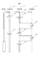
- FIG. 2 is a sequence diagram for explaining the processing flow of the electronic control device 10.
- the process shown in FIG. 2 is executed by the electronic control device 10.
- the start-up process of the internal processing unit 120 is divided into two stages, the first half is called “first start-up process” and the second half is called “second start-up process”.
- step S300 the power of the electronic control device 10 is turned on, and electricity is supplied to the internal processing unit 120, the external processing unit 200, and the transfer control unit 110.
- the left end of FIG. 2 shows a time-series change in the processing capacity of the electronic control device 10 for processing communication data. This processing capacity indicates that the wider the width in the horizontal direction shown in the figure, the higher the processing capacity.
- step S301 the external security verification unit 220 verifies whether the program or data of the external processing unit 200 has been tampered with.
- the external processing unit 200 proceeds to step S302 and activates the program to transition to a state in which communication data transfer processing is possible, that is, a routing acceptance state.
- a routing acceptance state when the communication data is received, the external control unit 210 rewrites the transfer destination of the communication header based on the external route information 231 and transmits the communication data to the communication unit 111 of the transfer control unit 110, thereby transmitting the communication data to another. Transfer to the device of.
- step S303 which is the first activation process of the internal processing unit 120
- the internal security verification unit 122 verifies the safety of the program and data related to the setting of the transfer information 114 of the transfer control unit 110, not the entire internal processing unit 120.
- the output destination setting unit 123 of the internal processing unit 120 and the initial information 126 are securely booted.
- the internal processing unit 120 proceeds to step S304 when the output destination setting unit 123 and the initial information 126 become available.
- step S304 the output destination setting unit 123 writes the initial information 126 to the transfer storage unit 113 of the transfer control unit 110 to generate the transfer information 114.
- the transfer information 114 generated in step S304 has an external processing unit 200 set as one of the transfer destinations, and the communication data received by the transfer control unit 110 can be transferred to the external processing unit 200. Since the external processing unit 200 is in the routing accepting state, the routing function is operated. In the transfer information 114 generated in step S304, the internal processing unit 120 is not included in the transfer destination.
- step S305 The internal processing unit 120 proceeds to step S305 when the writing to the transfer storage unit 113 by the output destination setting unit 123 is completed.
- step S305 which is the second activation process of the internal processing unit 120, the internal security verification unit 122 performs secure booting on the remaining programs and data that were not secure booted in step S303 described above. Specifically, the internal security verification unit 122 performs secure boot for the internal control unit 121, the internal route information 125, and the transfer update information 127. When these secure boots are completed, the process proceeds to step S306.
- step S306 the internal processing unit 120 updates the transfer information 114 by writing the transfer update information 127 to the transfer storage unit 113 by the output destination setting unit 123. By this update, the internal processing unit 120 is included in the transfer destination of the transfer information 114.
- step S307 the internal processing unit 120 transitions to a state in which communication data can be transferred, that is, a routing acceptance state, and transfers the communication data received from the transfer control unit 110 according to the transfer information 114.
- step S304 Since the communication data cannot be processed until step S304 is completed, the processing capacity is zero.
- step S304 the transfer control unit 110 and the external processing unit 200 can process the communication data.
- step S306 the transfer control unit 110, the external processing unit 200, and the internal processing unit 120 can process the communication data, so that the processing capacity is increased.
- FIG. 3 is a flowchart showing a detailed processing procedure of the internal processing unit 120.
- step S400 the internal security verification unit 122 executes secure boot, and confirms that the function related to writing to the transfer information 114 of the transfer control unit 110 has not been tampered with. Specifically, the output destination setting unit 123 and the initial information 126 of the internal processing unit 120 are securely booted.
- step S401 the internal processing unit 120 confirms whether or not the secure boot performed in step S400 was successful and could be started.
- the process proceeds to step S402, the processing is stopped, and the processing of FIG. 3 is completed.
- the process proceeds to step S403.
- step S403 the internal processing unit 120 confirms whether the secure boot of the external processing unit 200 has been completed and is already in the routing acceptance state. In this step, when it is known that the secure boot of the external processing unit 200 is completed in a shorter time than the secure boot of the internal processing unit 120 is completed, or when the transfer function is to be activated in a shorter time. You may skip it depending on the situation.
- the internal processing unit 120 determines that the external processing unit 200 is in the routing acceptance state, the internal processing unit 120 proceeds to step S404.
- step S402 stops the processing, and ends the processing of FIG.
- step S404 the output destination setting unit 123 creates the transfer information 114 by writing the information of the initial information 126 to the transfer storage unit 113 of the transfer control unit 110.
- the transfer function is already in operation when step S404 is completed.
- step S405 the internal security verification unit 122 executes a secure boot for the remaining programs and data of the internal processing unit 120 whose safety has not been verified in step S400. Specifically, the internal control unit 121, the internal route information 125, and the transfer update information 127 are securely booted.
- step S406 the internal processing unit 120 confirms whether or not the secure boot performed in step S405 was successful.
- the process proceeds to step S407, and when it determines that the secure boot has failed, the internal processing unit 120 proceeds to step S402, stops the process, and ends the process of FIG.
- step S407 the output destination setting unit 123 updates the transfer information 114 by writing the information of the transfer update information 127 to the transfer storage unit 113 of the transfer control unit 110 by the output destination setting unit 123.
- step S408 the internal processing unit 120 is in the routing acceptance state, the communication data received by the transfer control unit 110 can be processed, and the processing shown in FIG. 3 is completed.
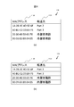
- FIG. 4 is a diagram showing an example of transfer information 114.
- FIG. 4A is transfer information 114 created by the processing of step S304 of FIG. 2 and step S404 of FIG.
- FIG. 4B is transfer information 114 created by step S306 of FIG. 2 and step S407 of FIG.
- the transfer information 114 shown in FIG. 4A is referred to as “before update” transfer information 114
- the transfer information 114 shown in FIG. 4B is referred to as “after update” transfer information 114.
- the transfer information 114 is composed of a MAC address 1130 and a transfer destination 1131.
- the MAC address 1130 is used to identify the received communication data and investigate the registered transfer destination.
- the transfer destination 1131 describes the transfer destination of the received communication data. For example, the port numbers connected to the internal processing unit 120, the external processing unit 200, and the second device 20 and the third device 30 are described.
- the communication data received before the update of the transfer information 114 is not transferred to the internal processing unit 120, but is transferred to either device or the external processing unit 200. This is because the transfer function of the internal processing unit 120 has not been activated yet, so that the transfer information 114 before the update is created with the intention of avoiding the transfer to the internal processing unit 120.
- the transfer destination MAC address included in the communication header is rewritten in the communication data received by the transfer control unit 110 from the internal processing unit 120 and the external processing unit 200. Therefore, the transfer information control unit 112 refers to the transfer information 114 again, searches for the transfer destination, and transmits the transfer information to the corresponding transfer destination.
- FIG. 4 shows an example in which the MAC address 1130 is used for identifying the communication data
- another value may be used as long as the transfer destination of the communication data can be determined.
- the transfer destination may be determined by using a part of the value of the MAC address 1130, or by using the IP address or a part thereof.
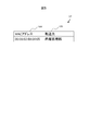
- FIG. 5 is a diagram showing an example of transfer update information 127.
- the transfer update information 127 is an update portion of the transfer information 114, for example, a difference between FIGS. 4 (a) and 4 (b).
- the output destination setting unit 123 refers to the transfer information 114 stored in the transfer storage unit 113, and when the MAC addresses of the transfer update information 127 match, the information stored in the transfer destination 1131 is used as the information of the transfer destination 1261. Update.
- the transfer destination of the MAC address "00:01:02:03:05" is updated to the internal processing unit 120.
- the external processing unit 200 and the internal processing unit 120 distribute the processing after the update.
- the external processing unit 200 may not perform the communication data transfer processing, and the internal processing unit 120 may process all the communication data.
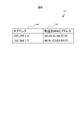
- FIG. 6 is a diagram showing an example of internal route information 125.
- the internal route information 125 is composed of an IP address 1240 and a forwarding MAC address 1241.
- the internal control unit 121 refers to the internal route information 125, searches for the MAC address of the transfer destination from the IP address included in the header of the received communication data, rewrites the header information to the searched MAC address, and transmits the header information to the transfer control unit 110. To do. For example, when communication data with a MAC address of "00:01:02:03:04:05" and an IP address of "255.255.1.3" is received, the transfer destination MAC address is searched from the database and communication is performed. The header is rewritten from "00:01:02:03:04:05" to "1A: 2B: 3C: 4D: 5E: 6F".
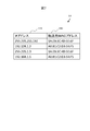
- FIG. 7 is a diagram showing an example of external route information 231.
- the data structure of the external route information 231 is the same as that of the internal route information 125 of FIG. Since the external processing unit 200 needs to rewrite the transfer destination MAC address of the communication data even for the communication data received before the internal processing unit 120 operates, the external route information 231 is the internal route information 125. The amount of data is larger than that.
- the electronic control device 10 includes an external processing unit 200 (first processing unit), an internal processing unit 120 (second processing unit), and a transfer control unit 110.
- the internal processing unit 120 requires a longer time for startup processing than the external processing unit 200.
- the transfer control unit 110 can transfer the communication data received from the outside to the external processing unit 200 and the internal processing unit 120.
- the transfer control unit 110 does not use the internal processing unit 120 as the data transfer destination from the start to the completion of the start processing of the internal processing unit 120, and includes the external processing unit 200 as the transfer destination.
- FIG. 4B when the activation process of the internal processing unit 120 is completed, at least the internal processing unit 120 is set as the data transfer destination.
- the communication data can be processed even before the internal processing unit 120 completes the activation process, and the processing capacity of the communication data received at the time of activation is guaranteed. Further, when the activation processing of the internal processing unit 120 is completed, the communication data is processed by using the internal processing unit 120, so that the processing capacity is improved.
- the transfer control unit 110 does not process any communication data until the entire startup processing of the internal processing unit 120 and the external processing unit 200 is completed. In that case, the processing capacity is zero until the entire startup process is completed.
- the communication data is processed by the transfer control unit 110 and the internal processing unit 120 even if the activation processing of the external processing unit 200 is not completed, so that the processing is performed from the time of activation even though the processing capacity is low. Can be started. That is, in the present embodiment, the period in which the processing capacity is zero can be shortened.
- the transfer control unit 110 includes a transfer storage unit 113 that stores transfer information 114, which is correspondence information between a data identifier and a data transfer destination.
- the transfer control unit 110 determines the data transfer destination with reference to the transfer information 114.
- the transfer destination of the communication data is changed by rewriting the transfer information 114 by the internal processing unit 120.
- the transfer control unit 110 transfers the data to any of the transfer destinations including the external processing unit 200 and the internal processing unit 120 with reference to the transfer information 114. Therefore, when the start processing of the internal processing unit 120 is completed, not only the external processing unit 200 but also the internal processing unit 120 is used to execute the communication data transfer processing, so that the processing becomes faster.
- the internal processing unit 120 includes an internal security verification unit 122 (second security verification unit) that detects tampering.
- the internal processing unit 120 uses the internal security verification unit 122 to detect falsification of at least one configuration other than the internal security verification unit 122 that constitutes the internal processing unit 120 as part of the activation process.
- the transfer control unit 110 includes a transfer storage unit 113 that stores transfer information 114, which is correspondence information between a data identifier and a data transfer destination.
- the transfer control unit 110 determines the data transfer destination with reference to the transfer information 114.
- the internal processing unit 120 includes an internal security verification unit 122 (second security verification unit) that detects tampering.
- the activation process of the internal processing unit 120 includes a first activation process of S303 in FIG. 2 and a second activation process of S305 of FIG.
- the internal security verification unit 122 falsifies the program that realizes the output destination setting unit 123 that rewrites the transfer information 114, and the initial information 126 that is information that the internal processing unit 120 is not the data transfer destination.
- the output destination setting unit 123 writes the initial information 126 to the transfer storage unit 113. Therefore, the internal security verification unit 122 can be used to create secure transfer information 114 that has been confirmed not to have been tampered with.
- both the internal processing unit 120 and the external processing unit 200 perform secure boot.
- at least one of the internal processing unit 120 and the external processing unit 200 does not have to perform secure boot.
- the case where secure boot does not need to be performed is, for example, the case where a program or data is stored in a read-only memory, or the case where the possibility of falsification does not need to be considered.
- Even when secure boot is not performed when the startup of the external processing unit 200 takes longer than that of the internal processing unit 120 due to, for example, a large data size of a program or data, the present embodiment The configuration of is valid.
- the external processing unit 200 becomes one of the transfer destinations from the transfer control unit 110 until the startup processing of the external processing unit 200, which has a long start processing, is completed, and when the startup processing of the external processing unit 200 is completed, the external processing unit 200 is external. Since the processing unit 200 and the internal processing unit 120 are included in the transfer destination from the transfer control unit 110, the communication data processing can be started before the activation processing is completed.
- the output destination setting unit 123 of the internal processing unit 120 writes to the transfer storage unit 113 of the transfer control unit 110.
- the internal processing unit 120 may transmit a write command to the transfer control unit 110, and the transfer control unit 110 may write to the transfer storage unit 113.
- the transfer control unit 110 is provided with the initial information 126 and the transfer update information 127.
- the internal processing unit 120 transmits a rewrite command to the transfer control unit 110, and the transfer control unit 110 rewrites the transfer information 114 by itself.
- the internal control unit 121 and the output destination setting unit 123 are realized by executing a program by a CPU (not shown).
- the internal control unit 121 and the output destination setting unit 123 may be realized by using an FPGA (Field Programmable Gate Array) which is a rewritable logic circuit.
- FPGA Field Programmable Gate Array
- the internal security verification unit 122 detects falsification of the configuration data as a secure boot process.
- the internal security verification unit 122 calculates the signature value of the configuration data in the same manner as the program, and determines whether or not the signature value has been tampered with depending on whether or not the signature value matches the value recorded in advance.
- program and configuration data are similar in terms of the program code that realizes the above-mentioned functional block, although the target to be read is different.
- program and the configuration data are collectively referred to as "program realization data". According to this modification 5, even when the configuration of the electronic control device 10 includes the FPGA, the same effect as that of the first embodiment can be obtained.
- a part of the communication data can be processed only by the transfer control unit 110.
- the communication data having the two MAC addresses from the top shown in FIG. 4A is not transferred to the internal processing unit 120 or the external processing unit 200, and the processing is completed only by the transfer control unit 110.
- the transfer control unit 110 may always transfer the communication data to the internal processing unit 120 or the external processing unit 200 without completing the processing only by the transfer control unit 110.
- the internal control unit 121 and the external control unit 210 have rewritten the header information of the received communication data. However, at least one of the internal control unit 121 and the external control unit 210 does not have to rewrite the header information of the received communication data. In this case, the internal control unit 121 and the external control unit 210 perform some processing using the communication data. This process is, for example, a process of determining whether or not the communication data complies with a predetermined rule, and discarding the communication data if the communication data does not comply with the predetermined rule.
- the locations of the internal processing unit 120 and the external processing unit 200 may be interchanged. That is, the external processing unit 200 may be included in the data transfer unit 100, and the internal processing unit 120 may exist outside the data transfer unit 100.
- FIGS. 8 to 10 A second embodiment of the electronic control device will be described with reference to FIGS. 8 to 10.
- the same components as those in the first embodiment are designated by the same reference numerals, and the differences will be mainly described.
- the points not particularly described are the same as those in the first embodiment.
- This embodiment is different from the first embodiment mainly in that there is no risk of falsification of some programs.
- FIG. 8 is a configuration diagram of the electronic control device 10A according to the second embodiment.
- the same components as those of the electronic control device 10 in the first embodiment are designated by the same reference numerals, and the description thereof will be omitted.
- the program that realizes the output destination setting unit 123 of the internal processing unit 120 and the initial information 126 are stored in the non-rewritable memory area 129 such as the HSM or OTP (One Time Program) area. That is, the program that realizes the function required for writing to the transfer storage unit 113 of the transfer control unit 110 and the information to be written to the transfer storage unit 113 are to be stored in the non-rewritable area.
- FIG. 9 is a sequence diagram showing the operation of the electronic control device 10A in the second embodiment.
- the same processing as in FIG. 2 is assigned the same number, and the description thereof will be omitted.
- the method of activating the process immediately after the start of operation of the internal processing unit 120 that is, the function for activating the function for writing to the transfer storage unit 113 of the transfer control unit 110 is different.
- step S900 the internal processing unit 120 activates the program that writes to the transfer storage unit 113, that is, the output destination setting unit 123, and reads the initial information 126.
- the program for realizing the output destination setting unit 123 and the initial information 126 are stored in the non-writable area and there is no risk of falsification, the verification by the internal security verification unit 122 can be omitted. Since the subsequent processing is the same as that of the first embodiment, the description thereof will be omitted.
- FIG. 10 is a flowchart showing the processing of the internal processing unit 120 in the second embodiment.
- the same processing as that of the step shown in FIG. 3 is assigned the same number and the description thereof will be omitted.
- steps S400 and S401 are replaced by steps S900.
- step S1000 since the program related to writing the transfer information 114 is stored in the HSM, there is no risk of falsification, so the output destination-related part is read and started without secure booting. Specifically, the output destination setting unit 123 and the initial information 126 are called.
- the transfer control unit 110 of the electronic control device 10A includes a transfer storage unit 113 that stores transfer information 114, which is correspondence information between the data identifier and the data transfer destination.
- the transfer control unit 110 determines the data transfer destination with reference to the transfer information 114.
- the start-up process of the internal processing unit 120 is composed of a first start-up process and a second start-up process. In the first activation process, the program code that realizes the output destination setting unit 123 in which the internal security verification unit 122 rewrites the transfer information 114 from the read-only area, and the information that the internal processing unit 120 is not used as the data transfer destination.
- the initial information 126 is read out, and the output destination setting unit 123 writes the initial information 126 to the transfer storage unit 113. Therefore, in the present embodiment, the internal security verification unit 122 does not require secure boot of the output destination setting unit 123 and the initial information 126, so that the first process can be completed earlier than in the first embodiment.
- FIGS. 11 to 12 A third embodiment of the electronic control device will be described with reference to FIGS. 11 to 12.
- the same components as those in the first embodiment are designated by the same reference numerals, and the differences will be mainly described.
- the points not particularly described are the same as those in the first embodiment.
- the present embodiment is different from the first embodiment mainly in that the transfer information is rewritten at the end.
- FIG. 11 is a configuration diagram of the electronic control device 10B according to the third embodiment.
- the internal processing unit 120 further includes a final processing unit 128.
- the processing of the internal security verification unit 122 and the output destination setting unit 123 is different from that of the first embodiment.
- the transfer storage unit 113 is a non-volatile storage device such as a flash memory, a phase change memory, or a magnetic memory. Therefore, when power is supplied to the electronic control device 10B, the information stored when the power supply is stopped remains in the transfer storage unit 113 as it is.
- the electronic control device 10B receives an operation stop command signal before the power supply from the outside is stopped.
- the output destination setting unit 123 writes the initial information 126 to the transfer storage unit 113, and the transfer information 114 includes the internal processing unit 120 as the transfer destination as shown in FIG. 4A. Rewrite to something that cannot be done. After this rewriting, the power supply to the electronic control device 10B is stopped.
- each of the internal processing unit 120 and the external processing unit 200 starts secure boot.
- the internal security verification unit 122 of the internal processing unit 120 targets the internal control unit 121, the output destination setting unit 123, the internal route information 125, and the transfer update information 127 for secure booting. That is, the initial information 126 is not subject to secure boot at startup. The initial information 126 is verified at a timing when the processing load after startup is low.
- the internal processing unit 120 writes the transfer update information 127 to the transfer storage unit 113 using the output destination setting unit 123, so that the transfer information 114 is internally stored in the transfer destination as shown in FIG. 4 (b). It is rewritten to include the processing unit 120. When this rewriting is completed, the internal processing unit 120 transitions to the routing acceptance state.
- FIG. 12 is a sequence diagram showing the operation of the electronic control device 10B according to the third embodiment. The same numbers are assigned to the processes similar to those of the first embodiment and the second embodiment, and the description thereof will be omitted.
- the transfer information 114 at this time includes the internal processing unit 120 at the transfer destination.
- the output destination setting unit 123 of the internal processing unit 120 performs the following processing. That is, the output destination setting unit 123 reads the initial information 126 from the internal storage unit 124 in step S910 and writes it to the transfer storage unit 113 of the transfer control unit 110 in step S314. After the completion of this writing, the power supply of the internal processing unit 120 ends. Then, in step S300, power is supplied to the internal processing unit 120.
- the external processing unit 200 performs secure boot in step S301 as in the first embodiment, and when completed, transitions to the routing acceptance state (step S302).
- step S301 the process corresponding to S304 in the first embodiment is completed by the rewriting in step S314 immediately before the power is turned off. Therefore, when the external processing unit 200 transitions to the routing acceptance state in step S302, the routing processing using the external processing unit 200 becomes possible.
- the transfer storage unit 113 is a non-volatile storage area.
- an end processing unit 128 that rewrites the transfer information 114 so that the transfer destination does not include the internal processing unit 120 is provided. Therefore, the electronic control device 10B can start the processing of the transferred data earlier than the first embodiment and the second embodiment.
- FIGS. 13 to 14 A fourth embodiment of the electronic control device will be described with reference to FIGS. 13 to 14.
- the same components as those in the first embodiment are designated by the same reference numerals, and the differences will be mainly described.
- the points not particularly described are the same as those in the first embodiment.
- the present embodiment is different from the first embodiment in that it mainly corresponds to the case where either the internal processing unit or the external processing unit completes the start-up process first.
- FIG. 13 is a configuration diagram of the electronic control device 10C according to the fourth embodiment.
- the same components as those of the electronic control device 10 in the first embodiment are designated by the same reference numerals, and the description thereof will be omitted.
- the internal processing unit 120 in the present embodiment further includes an internal determination unit 961 in addition to the configuration in the first embodiment. Further, the internal storage unit 124 stores the internal initial information 951 instead of the initial information 126.
- the external processing unit 200 in the present embodiment includes an external determination unit 962 and an external output destination setting unit 963 in addition to the configuration in the first embodiment. External initial information 952 is stored in the external storage unit 230.
- the internal security verification unit 122 of the internal processing unit 120 performs a secure boot of the internal control unit 121, the output destination setting unit 123, the internal determination unit 961, the internal route information 125, and the internal initial information 951 at the time of startup.
- the internal processing unit 120 performs secure boot in two stages, but in the present embodiment, all of these are processed at once.
- the external security verification unit 220 of the external processing unit 200 performs a secure boot of the external control unit 210, the external determination unit 962, the external output destination setting unit 963, the external route information 231 and the external initial information 952 at the time of startup.
- the internal initial information 951 is data related to the transfer destination of the received communication data, and the internal processing unit 120 is set in at least one of the transfer destinations, and the external processing unit 200 is not included in the transfer destination.
- the external initial information 952 is data related to the transfer destination of the received communication data, and the external processing unit 200 is set to at least one of the transfer destinations, and the internal processing unit 120 is not included in the transfer destination.
- the external initial information 952 is shown in FIG. 4A, for example.
- the internal determination unit 961 performs the following operation when the secure boot of the internal processing unit 120 is completed.
- the internal determination unit 961 determines whether or not the secure boot of the external processing unit 200 has been completed. Whether or not the secure boot of the external processing unit 200 is completed may be determined by, for example, the internal determination unit 961 reading the contents of the transfer storage unit 113, or the internal processing unit 120 and the external processing unit 200 for secure booting. May be realized by sending signals to each other that the above is completed.
- the output destination setting unit 123 is used to write the internal initial information 951 to the transfer storage unit 113, and the internal processing unit 120 is included as the transfer destination.
- the transfer information 114 is created.
- the internal determination unit 961 determines that the secure boot of the external processing unit 200 has been completed, it writes to the transfer storage unit 113 using the output destination setting unit 123, and the internal processing unit 120 and the external processing are sent to the transfer destination of the transfer information 114.
- the state including both parts 200 for example, the state shown in FIG. 4B is rewritten.
- the external determination unit 962 performs the following operation when the secure boot of the external processing unit 200 is completed.
- the external determination unit 962 determines whether or not the secure boot of the internal processing unit 120 is completed. This determination can be realized by the same method as that of the internal determination unit 961.
- the external output destination setting unit 963 is used to write the external initial information 952 to the transfer storage unit 113, and the external processing unit 200 is used as the transfer destination.
- the transfer information 114 including the transfer information 114 is created.
- the external output destination setting unit 963 is used to write to the transfer storage unit 113, and the internal processing unit 120 and the external are connected to the transfer destination of the transfer information 114.
- the state including both of the processing units 200, for example, the state shown in FIG. 4B is rewritten.
- FIG. 14 is a sequence diagram illustrating a processing flow of the electronic control device 10C according to the fourth embodiment.
- Step S911 and step S921 are started at the same time.
- the external security verification unit 220 starts secure boot.
- the internal security verification unit 122 starts secure boot.
- the internal determination unit 961 starts operation and determines whether or not the secure boot by the external processing unit 200 is completed.
- the internal determination unit 961 writes the internal initial information 951 to the transfer storage unit 113 in step S931 and transitions to the routing acceptance state in step S922.
- the external processing unit 200 determines that the external determination unit 962 has already completed the secure boot of the internal processing unit 120. Then, the external determination unit 962 rewrites the transfer information 114 in step S932, and the external processing unit 200 transitions to the routing acceptance state in step S912.
- the transfer data processing using the one started first can be started.
- the information described in the transfer information 114 changes depending on which of the internal processing unit 120 and the external processing unit 200 is started first, but the information described in the transfer information 114 is not changed.
- the name of the configuration may be changed to.
- the internal processing unit 120 and the external processing unit 200 are tentatively called the first calculation unit and the second calculation unit, and the information to be written in the transfer information 114 is the same as in the first embodiment. That is, as shown in FIG. 4A, the transfer destination of the transfer information 114 created first includes the external processing unit 200 but not the internal processing unit 120.
- the operation in the present embodiment can be expressed. That is, the present embodiment can also be expressed as follows.
- each of the internal processing unit 120 and the external processing unit 200 is either a first calculation unit or a second calculation unit.
- the electronic control device 10C rewrites the transfer information 114 by using the first calculation unit and the second calculation unit for which the start processing is completed first as the external processing unit 200, and the start processing of the first calculation unit and the second calculation unit. It is provided with a determination unit for rewriting the transfer information 114, that is, an internal determination unit 961 and an external determination unit 962, with the one completed later as the internal processing unit 120. Therefore, regardless of which of the internal processing unit 120 and the external processing unit 200 is started first, the processing of the transfer data using the one started first can be started.
- the configuration of the functional block is only an example.
- Several functional configurations shown as separate functional blocks may be integrally configured, or the configuration represented by one functional block diagram may be divided into two or more functions. Further, a part of the functions possessed by each functional block may be provided in the other functional blocks.
Landscapes
- Engineering & Computer Science (AREA)
- Theoretical Computer Science (AREA)
- General Engineering & Computer Science (AREA)
- Physics & Mathematics (AREA)
- General Physics & Mathematics (AREA)
- Software Systems (AREA)
- Computer Hardware Design (AREA)
- Computer Security & Cryptography (AREA)
- Mathematical Physics (AREA)
- General Health & Medical Sciences (AREA)
- Health & Medical Sciences (AREA)
- Bioethics (AREA)
- Mechanical Engineering (AREA)
- Stored Programmes (AREA)
- Computer And Data Communications (AREA)
Abstract
Description
本発明の第2の態様による演算方法は、第1処理部、第2処理部、および転送制御部を備える電子制御装置が実行する演算方法であって、前記第1処理部よりも前記第2処理部は起動処理に長い時間を要し、前記転送制御部は、外部から受信する通信データを前記第1処理部および前記第2処理部に転送可能であり、前記第1処理部が、前記転送制御部から転送される前記通信データを処理することと、前記第2処理部は、前記転送制御部から転送される前記通信データを処理することと、前記転送制御部は、前記第2処理部の起動処理が完了するまでは前記第2処理部を前記通信データの転送先とせず前記第1処理部を転送先に含め、前記第2処理部の起動処理が完了すると少なくとも前記第2処理部を前記通信データの転送先とすることとを含む。
以下、図1~図7を参照して、電子制御装置の第1の実施の形態を説明する。
(1)電子制御装置10は、外部処理部200(第1処理部)、内部処理部120(第2処理部)、および転送制御部110を備える。外部処理部200よりも内部処理部120は起動処理に長い時間を要する。転送制御部110は、外部から受信する通信データを外部処理部200および内部処理部120に転送可能である。転送制御部110は、図4(a)に示すように起動から内部処理部120の起動処理が完了するまでは内部処理部120をデータの転送先とせず外部処理部200を転送先に含め、図4(b)に示すように内部処理部120の起動処理が完了すると少なくとも内部処理部120をデータの転送先とする。そのため、内部処理部120が起動処理が完了する以前であっても通信データの処理が可能であり、起動時に受信した通信データの処理能力が担保される。また、内部処理部120の起動処理が完了すれば内部処理部120を用いて通信データを処理するため、処理能力が向上する。
上述した第1の実施の形態では、データ転送部100は転送制御部110と内部処理部120とを独立した構成として説明した。しかし、転送制御部110と内部処理部120とが明示的に分離されない構成でもよい。
上述した第1の実施の形態では、内部処理部120および外部処理部200の両者ともセキュアブートを行った。しかし内部処理部120および外部処理部200の少なくとも一方は、セキュアブートを行わなくてもよい。セキュアブートを行わなくてもよい場合とはたとえば、プログラムやデータが読み出し専用のメモリに格納される場合や、改竄の可能性を考慮しなくてよい場合などである。セキュアブートを行わない場合であっても、たとえばプログラムやデータのデータサイズが大きいことなどを理由として外部処理部200の起動が内部処理部120よりも長時間を要する場合には、本実施の形態の構成が有効である。すなわち、起動処理に長時間を有する外部処理部200の起動処理が完了するまでは外部処理部200が転送制御部110からの転送先の1つとなり、外部処理部200の起動処理が完了すると外部処理部200および内部処理部120が転送制御部110からの転送先に含まれることで、起動処理が完了する前に通信データの処理を開始できる。
上述した第1の実施の形態では、内部処理部120の出力先設定部123が転送制御部110の転送記憶部113に書き込みを行った。しかし内部処理部120は転送制御部110に書き込みの指令を送信して転送制御部110が転送記憶部113への書き込みを行ってもよい。この場合には、初期情報126および転送更新情報127が転送制御部110に備えられる。内部処理部120が転送制御部110に書き換え指令を送信し、転送制御部110が自ら転送情報114を書き換える。
上述した第1の実施の形態では、内部処理部120の起動処理が完了すると、内部処理部120および外部処理部200の両方を転送先に含むように転送情報114が書き換えられた。しかし転送情報114は、内部処理部120の起動処理が完了すると、内部処理部120は転送先に含むが外部処理部200は転送先に含まないように書き換えられてもよい。この場合はたとえば、内部処理部120の起動処理が完了すると転送情報114は、図4(b)の3行目における「外部処理部」を「内部処理部」に書き換えたものとなる。本変形例によれば、内部処理部120の起動処理が完了すると外部処理部200は通信データの転送処理を行わないので、外部処理部200は別の処理を実行することができる。
上述した第1の実施の形態では、内部制御部121および出力先設定部123は不図示のCPUがプログラムを実行することにより実現された。しかし内部制御部121および出力先設定部123は、書き換え可能な論理回路であるFPGA(Field Programmable Gate Array)を用いて実現されてもよい。FPGAに書き込むコンフィギュレーションデータが書き換え可能な記憶領域に格納される場合には、内部セキュリティ検証部122はセキュアブートの処理として、コンフィギュレーションデータの改竄を検出する。内部セキュリティ検証部122は、コンフィギュレーションデータもプログラムと同様に署名値を計算し、その署名値が予め記録されている値と一致するか否かにより改竄されているか否かを判断する。
上述した第1の実施の形態では、通信データの一部は転送制御部110だけでも処理可能であった。たとえば図4(a)に示す上から2つのMACアドレスを有する通信データは、内部処理部120や外部処理部200に転送することなく転送制御部110だけで処理が完結した。しかし転送制御部110は、転送制御部110だけでは処理を完結させず通信データを常に内部処理部120や外部処理部200に転送してもよい。
内部制御部121および外部制御部210は、受信した通信データのヘッダ情報を書き換えた。しかし内部制御部121および外部制御部210の少なくとも一方は、受信した通信データのヘッダ情報を書き換えなくてもよい。この場合には内部制御部121および外部制御部210は、通信データを用いる何らかの処理を行う。この処理とはたとえば、通信データが所定の規則に従ったものであるか否かを判断し、所定の規則に従っていなければ通信データを破棄する処理である。
内部処理部120と外部処理部200は、その所在が入れ替わってもよい。すなわち外部処理部200がデータ転送部100に含まれ、内部処理部120はデータ転送部100の外部に存在してもよい。
図8~図10を参照して、電子制御装置の第2の実施の形態を説明する。以下の説明では、第1の実施の形態と同じ構成要素には同じ符号を付して相違点を主に説明する。特に説明しない点については、第1の実施の形態と同じである。本実施の形態では、主に、一部のプログラムの改竄の恐れがない点で、第1の実施の形態と異なる。
(6)電子制御装置10Aの転送制御部110は、データの識別子とデータの転送先の対応情報である転送情報114を格納する転送記憶部113を備える。転送制御部110は、転送情報114を参照してデータの転送先を決定する。内部処理部120の起動処理は、第1起動処理と第2起動処理とから構成される。第1起動処理では、読み出し専用領域から、内部セキュリティ検証部122が転送情報114を書き換える出力先設定部123を実現するプログラムコード、および内部処理部120をデータの転送先としない旨の情報である初期情報126を読み出し、出力先設定部123が初期情報126を転送記憶部113に書き込む。そのため、本実施の形態では内部セキュリティ検証部122が出力先設定部123および初期情報126のセキュアブートを要しないので、第1の実施の形態よりも早期に第1処理を完了できる。
図11~図12を参照して、電子制御装置の第3の実施の形態を説明する。以下の説明では、第1の実施の形態と同じ構成要素には同じ符号を付して相違点を主に説明する。特に説明しない点については、第1の実施の形態と同じである。本実施の形態では、主に、終了時に転送情報が書き換えられる点で、第1の実施の形態と異なる。
(7)転送記憶部113は不揮発性の記憶領域である。電子制御装置10Bの終了処理として、転送先に内部処理部120が含まれないように転送情報114を書き換える終了処理部128を備える。そのため電子制御装置10Bは、第1の実施の形態や第2の実施の形態よりも早期に転送データの処理を開始することができる。
図13~図14を参照して、電子制御装置の第4の実施の形態を説明する。以下の説明では、第1の実施の形態と同じ構成要素には同じ符号を付して相違点を主に説明する。特に説明しない点については、第1の実施の形態と同じである。本実施の形態では、主に、内部処理部と外部処理部のいずれが先に起動処理が完了する場合にも対応する点で、第1の実施の形態と異なる。
日本国特許出願2019-208977(2019年11月19日出願)
100…データ転送部
110…転送制御部
111…通信部
112…転送情報制御部
113…転送記憶部
114…転送情報
120…内部処理部
121…内部制御部
122…内部セキュリティ検証部
123…出力先設定部
124…内部記憶部
126…初期情報
127…転送更新情報
128…終了処理部
129…書換え不可のメモリ領域
200…外部処理部
210…外部制御部
220…外部セキュリティ検証部
230…外部記憶部
951…内部初期情報
952…外部初期情報
961…内部決定部
962…外部決定部
963…外部出力先設定部
Claims (14)
- 第1処理部、第2処理部、および転送制御部を備える電子制御装置であって、
前記第1処理部よりも前記第2処理部は起動処理に長い時間を要し、
前記転送制御部は、外部から受信する通信データを前記第1処理部および前記第2処理部に転送可能な通信部を備え、
前記第1処理部は、前記転送制御部から転送される前記通信データを処理する第1制御部を備え、
前記第2処理部は、前記転送制御部から転送される前記通信データを処理する第2制御部を備え、
前記転送制御部は、前記第2処理部の起動処理が完了するまでは前記第2処理部を前記通信データの転送先とせず前記第1処理部を転送先に含め、前記第2処理部の起動処理が完了すると少なくとも前記第2処理部を前記通信データの転送先とする、電子制御装置。 - 請求項1に記載の電子制御装置において、
前記転送制御部は、前記通信データの識別子と前記通信データの転送先の対応情報である転送情報を格納する転送記憶部をさらに備え、
前記転送制御部は、前記転送情報を参照して前記通信データの転送先を決定し、
前記転送制御部は、前記転送情報を自ら書き換えることにより前記通信データの転送先を変更する、または前記第2処理部により前記転送情報が書き換えられることにより前記通信データの転送先が変更される電子制御装置。 - 請求項2に記載の電子制御装置において、
前記転送制御部は、前記通信データの識別子と前記通信データの転送先の対応情報である転送情報を格納する転送記憶部をさらに備え、
前記転送制御部は、前記第2処理部の起動処理が完了すると前記転送情報を参照して前記通信データを、前記第1処理部および前記第2処理部を含む転送先のいずれかに転送する電子制御装置。 - 請求項2に記載の電子制御装置において、
前記第2処理部は、前記第2処理部の起動処理が完了すると前記転送記憶部の前記転送情報を転送先に前記第2処理部が含まれるように書き換える出力先設定部をさらに備える電子制御装置。 - 請求項2に記載の電子制御装置において、
前記転送記憶部は不揮発性の記憶領域であり、
前記電子制御装置の終了処理として、転送先に前記第2処理部が含まれないように前記転送情報を書き換える終了処理部をさらに備える電子制御装置。 - 請求項1に記載の電子制御装置において、
前記第2処理部は、改竄を検出する第2セキュリティ検証部を備え、
前記第2処理部は、前記第2処理部を構成する前記第2セキュリティ検証部を除く少なくとも1つの構成の改竄の検出を前記第2セキュリティ検証部を用いて前記起動処理の一部として行う電子制御装置。 - 請求項1に記載の電子制御装置において、
前記転送制御部は、前記通信データの識別子と前記通信データの転送先の対応情報である転送情報を格納する転送記憶部をさらに備え、
前記転送制御部は、前記転送情報を参照して前記通信データの転送先を決定し、
前記第2処理部は、改竄を検出する第2セキュリティ検証部を備え、
前記第2処理部の前記起動処理は、第1起動処理と第2起動処理とから構成され、
前記第1起動処理では、前記第2セキュリティ検証部が前記転送情報を書き換える出力先設定部を実現するプログラム実現データ、および前記第2処理部を前記通信データの転送先としない旨の情報である初期情報の改竄を検出し、前記出力先設定部が前記初期情報を前記転送記憶部に書き込む、電子制御装置。 - 請求項1に記載の電子制御装置において、
前記転送制御部は、前記通信データの識別子と前記通信データの転送先の対応情報である転送情報を格納する転送記憶部をさらに備え、
前記転送制御部は、前記転送情報を参照して前記通信データの転送先を決定し、
前記第2処理部の前記起動処理は、第1起動処理と第2起動処理とから構成され、
前記第1起動処理では、前記第2処理部が読み出し専用領域から、前記転送情報を書き換える出力先設定部を実現するプログラム実現データ、および前記第2処理部を前記通信データの転送先としない旨の情報である初期情報を読み出し、前記出力先設定部が前記初期情報を前記転送記憶部に書き込む、電子制御装置。 - 請求項1に記載の電子制御装置において、
前記第1処理部および前記転送制御部はデータ転送部に含まれ、前記第2処理部は前記データ転送部に接続される、電子制御装置。 - 請求項1に記載の電子制御装置において、
前記第2処理部および前記転送制御部はデータ転送部に含まれ、前記第1処理部は前記データ転送部に接続される、電子制御装置。 - 請求項9に記載の電子制御装置において、
前記データ転送部はデータリンク層またはネットワーク層におけるスイッチであり、
前記転送制御部はスイッチコアであり、
前記第1処理部は前記スイッチの内部プロセッサであり、
前記第2処理部は前記スイッチに接続されたマイコンである、電子制御装置。 - 請求項10に記載の電子制御装置において、
前記データ転送部はデータリンク層またはネットワーク層におけるスイッチであり、
前記転送制御部はスイッチコアであり、
前記第2処理部は前記スイッチの内部プロセッサであり、
前記第1処理部は前記スイッチに接続されたマイコンである、電子制御装置。 - 請求項2に記載の電子制御装置において、
前記第1処理部および前記第2処理部のそれぞれは、第1演算部および第2演算部のいずれかであり、
前記第1演算部および前記第2演算部のうち起動処理が先に完了した方を前記第1処理部として前記転送情報を書き換え、前記第1演算部および前記第2演算部のうち起動処理が後に完了した方を前記第2処理部として前記転送情報を書き換える決定部をさらに備える、電子制御装置。 - 第1処理部、第2処理部、および転送制御部を備える電子制御装置が実行する演算方法であって、
前記第1処理部よりも前記第2処理部は起動処理に長い時間を要し、
前記転送制御部は、外部から受信する通信データを前記第1処理部および前記第2処理部に転送可能であり、
前記第1処理部が、前記転送制御部から転送される前記通信データを処理することと、
前記第2処理部は、前記転送制御部から転送される前記通信データを処理することと、
前記転送制御部は、前記第2処理部の起動処理が完了するまでは前記第2処理部を前記通信データの転送先とせず前記第1処理部を転送先に含め、前記第2処理部の起動処理が完了すると少なくとも前記第2処理部を前記通信データの転送先とすることとを含む演算方法。
Priority Applications (2)
| Application Number | Priority Date | Filing Date | Title |
|---|---|---|---|
| US17/777,398 US12657145B2 (en) | 2019-11-19 | 2020-11-09 | Electronic control device and calculation method |
| CN202080079938.0A CN114746310B (zh) | 2019-11-19 | 2020-11-09 | 电子控制装置、电子控制方法 |
Applications Claiming Priority (2)
| Application Number | Priority Date | Filing Date | Title |
|---|---|---|---|
| JP2019-208977 | 2019-11-19 | ||
| JP2019208977A JP7373366B2 (ja) | 2019-11-19 | 2019-11-19 | 電子制御装置、演算方法 |
Publications (1)
| Publication Number | Publication Date |
|---|---|
| WO2021100527A1 true WO2021100527A1 (ja) | 2021-05-27 |
Family
ID=75965257
Family Applications (1)
| Application Number | Title | Priority Date | Filing Date |
|---|---|---|---|
| PCT/JP2020/041785 Ceased WO2021100527A1 (ja) | 2019-11-19 | 2020-11-09 | 電子制御装置、演算方法 |
Country Status (4)
| Country | Link |
|---|---|
| US (1) | US12657145B2 (ja) |
| JP (1) | JP7373366B2 (ja) |
| CN (1) | CN114746310B (ja) |
| WO (1) | WO2021100527A1 (ja) |
Cited By (1)
| Publication number | Priority date | Publication date | Assignee | Title |
|---|---|---|---|---|
| WO2026140762A1 (ja) * | 2024-12-24 | 2026-07-02 | 株式会社オートネットワーク技術研究所 | 車載装置、車載装置の起動方法、及び起動プログラム |
Citations (3)
| Publication number | Priority date | Publication date | Assignee | Title |
|---|---|---|---|---|
| US20100174895A1 (en) * | 2006-09-27 | 2010-07-08 | Pierce James R | Rapid-boot computing device with dual operating systems |
| JP2014085905A (ja) * | 2012-10-25 | 2014-05-12 | Nec Network & Sensor Systems Ltd | 通信装置、通信方法およびプログラム |
| JP2018116669A (ja) * | 2017-01-13 | 2018-07-26 | 株式会社オートネットワーク技術研究所 | 車載装置、中継装置及びコンピュータプログラム |
Family Cites Families (13)
| Publication number | Priority date | Publication date | Assignee | Title |
|---|---|---|---|---|
| JP2006352706A (ja) * | 2005-06-17 | 2006-12-28 | Hitachi Ltd | マイクロプロセッサ、ネットワークシステム及び通信方法 |
| JP2015022521A (ja) | 2013-07-19 | 2015-02-02 | スパンション エルエルシー | セキュアブート方法、組み込み機器、セキュアブート装置およびセキュアブートプログラム |
| JP6126980B2 (ja) * | 2013-12-12 | 2017-05-10 | 日立オートモティブシステムズ株式会社 | ネットワーク装置およびネットワークシステム |
| CN104724004B (zh) * | 2013-12-24 | 2017-10-13 | 坦亿有限公司 | 车辆系统的接口切换装置、方法与车辆系统 |
| US9705678B1 (en) * | 2014-04-17 | 2017-07-11 | Symantec Corporation | Fast CAN message authentication for vehicular systems |
| US9916453B2 (en) * | 2015-12-22 | 2018-03-13 | Qualcomm Incorporated | Derived keys for execution environments in a boot chain |
| US10262140B2 (en) * | 2016-09-29 | 2019-04-16 | Intel Corporation | Methods and apparatus to facilitate blockchain-based boot tracking |
| CN108337228B (zh) | 2017-01-13 | 2020-11-10 | 株式会社自动网络技术研究所 | 车载装置、中继装置以及介质 |
| JP2017121091A (ja) * | 2017-04-10 | 2017-07-06 | 日立オートモティブシステムズ株式会社 | Ecu、及び車用ネットワーク装置 |
| JP7087378B2 (ja) * | 2017-12-25 | 2022-06-21 | オムロン株式会社 | 制御システムおよび制御装置 |
| JP7003975B2 (ja) * | 2018-08-10 | 2022-01-21 | 株式会社デンソー | 車両情報通信システム,センター装置及びセンター装置のメッセージ送信方法 |
| US10991175B2 (en) * | 2018-12-27 | 2021-04-27 | Beijing Voyager Technology Co., Ltd. | Repair management system for autonomous vehicle in a trusted platform |
| US11290437B2 (en) * | 2018-12-27 | 2022-03-29 | Beijing Voyager Technology Co., Ltd. | Trusted platform protection in an autonomous vehicle |
-
2019
- 2019-11-19 JP JP2019208977A patent/JP7373366B2/ja active Active
-
2020
- 2020-11-09 CN CN202080079938.0A patent/CN114746310B/zh active Active
- 2020-11-09 WO PCT/JP2020/041785 patent/WO2021100527A1/ja not_active Ceased
- 2020-11-09 US US17/777,398 patent/US12657145B2/en active Active
Patent Citations (3)
| Publication number | Priority date | Publication date | Assignee | Title |
|---|---|---|---|---|
| US20100174895A1 (en) * | 2006-09-27 | 2010-07-08 | Pierce James R | Rapid-boot computing device with dual operating systems |
| JP2014085905A (ja) * | 2012-10-25 | 2014-05-12 | Nec Network & Sensor Systems Ltd | 通信装置、通信方法およびプログラム |
| JP2018116669A (ja) * | 2017-01-13 | 2018-07-26 | 株式会社オートネットワーク技術研究所 | 車載装置、中継装置及びコンピュータプログラム |
Cited By (1)
| Publication number | Priority date | Publication date | Assignee | Title |
|---|---|---|---|---|
| WO2026140762A1 (ja) * | 2024-12-24 | 2026-07-02 | 株式会社オートネットワーク技術研究所 | 車載装置、車載装置の起動方法、及び起動プログラム |
Also Published As
| Publication number | Publication date |
|---|---|
| US20220405226A1 (en) | 2022-12-22 |
| JP7373366B2 (ja) | 2023-11-02 |
| US12657145B2 (en) | 2026-06-16 |
| JP2021082002A (ja) | 2021-05-27 |
| CN114746310A (zh) | 2022-07-12 |
| CN114746310B (zh) | 2025-08-01 |
Similar Documents
| Publication | Publication Date | Title |
|---|---|---|
| CN107579848B (zh) | 实用拜占庭容错共识机制中动态更改共识节点的方法 | |
| JP2015036847A (ja) | 半導体装置 | |
| US10956144B2 (en) | Apparatus for providing update of vehicle and computer-readable storage medium | |
| US12608141B2 (en) | Storage controller and method of providing firmware image | |
| JP6968811B2 (ja) | ネットワークを通じて更新されることができるセキュアなブートコードキャッシュ | |
| CN107615714B (zh) | 通信装置及记录介质 | |
| CN109814934B (zh) | 数据处理方法、装置、可读介质和系统 | |
| CN113885907A (zh) | 一种固件升级系统及方法 | |
| CN115793507A (zh) | 在车辆的微控制器中使用多级安全验证来执行安全引导程序的方法和系统 | |
| JP2021117928A5 (ja) | ||
| CN112383402A (zh) | 双重幂等验证方法及服务器 | |
| JP7373366B2 (ja) | 電子制御装置、演算方法 | |
| CN115221527A (zh) | 电子装置及其控制方法 | |
| US12524311B2 (en) | Electronic control unit and storage medium storing software redundancy establishing program | |
| WO2021181828A1 (ja) | 車両制御装置及び車両制御システム | |
| CN116938495B (zh) | 数字证书的验证方法、装置、设备、系统及可读存储介质 | |
| CN116436766A (zh) | 实现网络Bypass功能的方法及电路 | |
| JPH0764868A (ja) | 記憶更新装置 | |
| US12307231B2 (en) | Information processing device, program update system, and program update method | |
| CN114629632A (zh) | 车载系统、通信方法以及非暂时性存储介质 | |
| JP2026002455A (ja) | 情報処理装置、車載システム、情報処理方法及びコンピュータプログラム | |
| CN111273919A (zh) | 一种支持软件批量远程更新的安全计算机平台 | |
| US12135875B2 (en) | I/O command control device and information storage device | |
| JP7472844B2 (ja) | 電子制御装置 | |
| CN121233150A (zh) | 基于ArtNet模块的应用编程方法 |
Legal Events
| Date | Code | Title | Description |
|---|---|---|---|
| 121 | Ep: the epo has been informed by wipo that ep was designated in this application |
Ref document number: 20890049 Country of ref document: EP Kind code of ref document: A1 |
|
| NENP | Non-entry into the national phase |
Ref country code: DE |
|
| 122 | Ep: pct application non-entry in european phase |
Ref document number: 20890049 Country of ref document: EP Kind code of ref document: A1 |
|
| WWG | Wipo information: grant in national office |
Ref document number: 202080079938.0 Country of ref document: CN |
|
| WWG | Wipo information: grant in national office |
Ref document number: 17777398 Country of ref document: US |