WO2021074331A1 - Device for regrowth of a thick structure, photonic device comprising the same and associated methods of fabrication - Google Patents
Device for regrowth of a thick structure, photonic device comprising the same and associated methods of fabrication Download PDFInfo
- Publication number
- WO2021074331A1 WO2021074331A1 PCT/EP2020/079114 EP2020079114W WO2021074331A1 WO 2021074331 A1 WO2021074331 A1 WO 2021074331A1 EP 2020079114 W EP2020079114 W EP 2020079114W WO 2021074331 A1 WO2021074331 A1 WO 2021074331A1
- Authority
- WO
- WIPO (PCT)
- Prior art keywords
- layer
- regrowth
- inp
- substrate
- cladding
- Prior art date
- Legal status (The legal status is an assumption and is not a legal conclusion. Google has not performed a legal analysis and makes no representation as to the accuracy of the status listed.)
- Ceased
Links
Classifications
-
- G—PHYSICS
- G02—OPTICS
- G02B—OPTICAL ELEMENTS, SYSTEMS OR APPARATUS
- G02B6/00—Light guides; Structural details of arrangements comprising light guides and other optical elements, e.g. couplings
- G02B6/10—Light guides; Structural details of arrangements comprising light guides and other optical elements, e.g. couplings of the optical waveguide type
- G02B6/12—Light guides; Structural details of arrangements comprising light guides and other optical elements, e.g. couplings of the optical waveguide type of the integrated circuit kind
- G02B6/12004—Combinations of two or more optical elements
-
- G—PHYSICS
- G02—OPTICS
- G02B—OPTICAL ELEMENTS, SYSTEMS OR APPARATUS
- G02B6/00—Light guides; Structural details of arrangements comprising light guides and other optical elements, e.g. couplings
- G02B6/10—Light guides; Structural details of arrangements comprising light guides and other optical elements, e.g. couplings of the optical waveguide type
- G02B6/12—Light guides; Structural details of arrangements comprising light guides and other optical elements, e.g. couplings of the optical waveguide type of the integrated circuit kind
- G02B6/12002—Three-dimensional structures
-
- H—ELECTRICITY
- H01—ELECTRIC ELEMENTS
- H01S—DEVICES USING THE PROCESS OF LIGHT AMPLIFICATION BY STIMULATED EMISSION OF RADIATION [LASER] TO AMPLIFY OR GENERATE LIGHT; DEVICES USING STIMULATED EMISSION OF ELECTROMAGNETIC RADIATION IN WAVE RANGES OTHER THAN OPTICAL
- H01S5/00—Semiconductor lasers
- H01S5/02—Structural details or components not essential to laser action
- H01S5/0206—Substrates, e.g. growth, shape, material, removal or bonding
- H01S5/0215—Bonding to the substrate
- H01S5/0216—Bonding to the substrate using an intermediate compound, e.g. a glue or solder
-
- H—ELECTRICITY
- H10—SEMICONDUCTOR DEVICES; ELECTRIC SOLID-STATE DEVICES NOT OTHERWISE PROVIDED FOR
- H10P—GENERIC PROCESSES OR APPARATUS FOR THE MANUFACTURE OR TREATMENT OF DEVICES COVERED BY CLASS H10
- H10P90/00—Preparation of wafers not covered by a single main group of this subclass, e.g. wafer reinforcement
- H10P90/19—Preparing inhomogeneous wafers
- H10P90/1904—Preparing vertically inhomogeneous wafers
- H10P90/1906—Preparing SOI wafers
- H10P90/1914—Preparing SOI wafers using bonding
-
- G—PHYSICS
- G02—OPTICS
- G02B—OPTICAL ELEMENTS, SYSTEMS OR APPARATUS
- G02B6/00—Light guides; Structural details of arrangements comprising light guides and other optical elements, e.g. couplings
- G02B6/10—Light guides; Structural details of arrangements comprising light guides and other optical elements, e.g. couplings of the optical waveguide type
- G02B6/12—Light guides; Structural details of arrangements comprising light guides and other optical elements, e.g. couplings of the optical waveguide type of the integrated circuit kind
- G02B2006/12035—Materials
- G02B2006/12061—Silicon
-
- G—PHYSICS
- G02—OPTICS
- G02B—OPTICAL ELEMENTS, SYSTEMS OR APPARATUS
- G02B6/00—Light guides; Structural details of arrangements comprising light guides and other optical elements, e.g. couplings
- G02B6/10—Light guides; Structural details of arrangements comprising light guides and other optical elements, e.g. couplings of the optical waveguide type
- G02B6/12—Light guides; Structural details of arrangements comprising light guides and other optical elements, e.g. couplings of the optical waveguide type of the integrated circuit kind
- G02B2006/12035—Materials
- G02B2006/12078—Gallium arsenide or alloys (GaAs, GaAlAs, GaAsP, GaInAs)
-
- G—PHYSICS
- G02—OPTICS
- G02B—OPTICAL ELEMENTS, SYSTEMS OR APPARATUS
- G02B6/00—Light guides; Structural details of arrangements comprising light guides and other optical elements, e.g. couplings
- G02B6/10—Light guides; Structural details of arrangements comprising light guides and other optical elements, e.g. couplings of the optical waveguide type
- G02B6/12—Light guides; Structural details of arrangements comprising light guides and other optical elements, e.g. couplings of the optical waveguide type of the integrated circuit kind
- G02B2006/12083—Constructional arrangements
- G02B2006/12128—Multiple Quantum Well [MQW]
-
- G—PHYSICS
- G02—OPTICS
- G02B—OPTICAL ELEMENTS, SYSTEMS OR APPARATUS
- G02B6/00—Light guides; Structural details of arrangements comprising light guides and other optical elements, e.g. couplings
- G02B6/10—Light guides; Structural details of arrangements comprising light guides and other optical elements, e.g. couplings of the optical waveguide type
- G02B6/12—Light guides; Structural details of arrangements comprising light guides and other optical elements, e.g. couplings of the optical waveguide type of the integrated circuit kind
- G02B2006/12166—Manufacturing methods
- G02B2006/12178—Epitaxial growth
-
- H—ELECTRICITY
- H01—ELECTRIC ELEMENTS
- H01S—DEVICES USING THE PROCESS OF LIGHT AMPLIFICATION BY STIMULATED EMISSION OF RADIATION [LASER] TO AMPLIFY OR GENERATE LIGHT; DEVICES USING STIMULATED EMISSION OF ELECTROMAGNETIC RADIATION IN WAVE RANGES OTHER THAN OPTICAL
- H01S5/00—Semiconductor lasers
- H01S5/02—Structural details or components not essential to laser action
- H01S5/0206—Substrates, e.g. growth, shape, material, removal or bonding
- H01S5/021—Silicon based substrates
-
- H—ELECTRICITY
- H01—ELECTRIC ELEMENTS
- H01S—DEVICES USING THE PROCESS OF LIGHT AMPLIFICATION BY STIMULATED EMISSION OF RADIATION [LASER] TO AMPLIFY OR GENERATE LIGHT; DEVICES USING STIMULATED EMISSION OF ELECTROMAGNETIC RADIATION IN WAVE RANGES OTHER THAN OPTICAL
- H01S5/00—Semiconductor lasers
- H01S5/02—Structural details or components not essential to laser action
- H01S5/0206—Substrates, e.g. growth, shape, material, removal or bonding
- H01S5/0215—Bonding to the substrate
-
- H—ELECTRICITY
- H01—ELECTRIC ELEMENTS
- H01S—DEVICES USING THE PROCESS OF LIGHT AMPLIFICATION BY STIMULATED EMISSION OF RADIATION [LASER] TO AMPLIFY OR GENERATE LIGHT; DEVICES USING STIMULATED EMISSION OF ELECTROMAGNETIC RADIATION IN WAVE RANGES OTHER THAN OPTICAL
- H01S5/00—Semiconductor lasers
- H01S5/30—Structure or shape of the active region; Materials used for the active region
- H01S5/34—Structure or shape of the active region; Materials used for the active region comprising quantum well or superlattice structures, e.g. single quantum well [SQW] lasers, multiple quantum well [MQW] lasers or graded index separate confinement heterostructure [GRINSCH] lasers
Definitions
- TECHNICAL FIELD [1] Various example embodiments relate to optical components, notably to photonic devices. More particularly, various embodiments relate to the fabrication of thick photonic devices fully regrown onto silicon. BACKGROUND
- silicon photonics lack efficient light emission and amplification.
- the integration of III-V semiconductors on top of silicon waveguide circuits is required to achieve complex integrated circuits.
- Heterogeneous integration through wafer bonding allows for dense and wafer-scale integration of the III-V optoelectronic components on the silicon photonic platform.
- III/V devices would require a precise alignment at the bonding step in order for each device to be well placed on the top silicon circuits. This alignment might be extremely difficult, is time consuming and could be quite expensive [4] That is why other approaches have been developed by many industrial manufacturers in order to offer a larger epitaxial tool kit to designers of silicon photonic devices.
- Mean Square of these structures are in the range of 10 nm, more than ten time higher than on the same structure regrown on an InP substrate. This higher roughness accounts for the lower material quality.
- surface roughness RMS it is meant in the frame of the present application is the Root Mean Square surface roughness average of the profile height deviations from the mean line, recorded within the evaluation length.
- the total thickness of the grown material is limited to typically a half micron.
- This thickness limitation directly impacts the achievable laser designs and has largely encouraged the "membrane buried heterostructure laser " technique where a thin MQW stack is laterally buried in order to form a p-i-n lateral junction instead of a thick vertical p-i-n junction.
- this thickness limitation directly impacts the achievable laser designs used in the conventional InP platform know-how, based on a thick vertical p-i-n junction.
- Example embodiments of the invention aims to remedy all or some of the disadvantages of the above identified prior art.
- a first example embodiment relates then to a device for regrowth of a thick structure lattice-matched with InP comprising: a Si substrate, an interface layer of Si0 2 on the Si substrate, a bonding layer on the interface layer, said bonding layer being made of a III-V material consisting of an alloy of the AlGalnAs material family. a regrowth layer on the bonding layer, said regrowth layer being made of InP.
- alloy of the AlGalnAs material family it is meant, in the present application, components comprising As and at least two elements chosen among of the group consisting of Al, Ga, and In.
- the device for regrowth according to the first example embodiment offers a way to put up with the effects of thermally induced stress and to allows the regrowth of a thick structure of
- III-V material lattice-matched with InP by using a specific Ill-
- V material at the bonding interface with Si0 2 /Si which offers a higher bonding strength. This enables to further increase the total thickness of III-V material.
- the interface layer of Si0 2 may comprise a silicon waveguide.
- the bonding layer AlGalnAs composition/material family is chosen to obtain an almost perfect lattice match with InP lattice parameter (with a tolerance usually better than 0.1% and typically around 0.01% or 100 PPM).
- the bonding layer may consist of GalnAs which has the advantage to form a stable interface with a thermal Si02.
- the bonding layer may consist of AlInAs which has the advantage that the material formed at the interface resulting from the reaction between AlInAs and thermal SiO 2 has a very high stability.
- AlxIm-xAs with 0.465 ⁇ x ⁇ 0.481 lattice matched to InP.
- a device comprising a bonding layer on the interface layer consisting in an InP/AlInAs (lOnm)-bonded-to- SiO 2 Si(substrate) stack offers a strong adherence which permits the bonding structure to resist an important strain energy due to the thermal coefficient expansion (GTE) mismatch and a thick regrowth.
- GTE thermal coefficient expansion
- This InP/AlInAs(lOnm)-bonded-to-Si0 2 /Si(sub) may serve for all kind of support for regrowth of a thick structure lattice- matched with InP. More particularly, for telecom-oriented applications, a 3 ⁇ m-thick vertical p-i-n junction, both for emission or reception, may be regrown, including cladding, active, contact layers.
- the thickness of the bonding layer may be comprised between 1 and 100 nm, preferably between 5 and 50 nm, and even more preferably between 8 and 12 nm.
- the thickness of the regrowth layer being made of InP may be of about 100 nm.
- a second example embodiment relates to a photonic device for combining a silicon "Si" material and a III-V material comprising: the device for regrowth of a thick structure lattice- matched with InP according to the first example embodiment, an inferior cladding on the regrowth layer of the device for regrowth according to the first example embodiment, said inferior cladding comprising at least one III-V material layer, at least an active layer on the inferior cladding, a superior cladding on the active layer, said superior cladding comprising at least one III-V material layer.
- the first and second III-V materials may be same or different.
- the active layer may be a Multiple Quantum
- the photonic device may be used as a light tuning device, such as optical waveguide, laser, modulator or optical amplifier.
- the active layer may be a thick absorption layer.
- the photonic device may be used as a light detector device.
- the surface roughness RMS of the superior cladding may be less than 1 nanometer.
- the total thickness of the inferior cladding, the active layer, and the superior cladding may be higher than 1 pm, and preferably of about 3 pm.
- the total thickness of the first III-V material layer, the active layer, the second III-V material layer and the third III-V material layer is higher than 1 micron, and preferably about 3 microns.
- a third example embodiment relates to a method of fabrication of a device for regrowth of a thick structure lattice-matched with
- InP comprising the following steps: providing a Si substrate; layering the Si substrate with an Si02 interface layer by thermal oxidation of said Si substrate; providing an InP substrate; layering a regrowth layer made of InP on the InP substrate; layering a bonding layer made of an alloy of the(AlGa)InAs family on the regrowth layer, by epitaxial growth so as to form a stack; bonding the SiO 2 interface layer and the bonding layer of the stack; removing the InP substrate.
- the step of bonding the SiO 2 interface layer and the bonding layer of the stack may be realized by hydrophilic direct bonding.
- the method of fabrication of a device for regrowth of a thick structure lattice-matched according to the third example embodiment may further comprise the following steps:
- the step of removing the stop-etch layer and the InP substrate may be preferably realized by chemical selective etching.
- the substrate might be partially removed using a grinding step to minimize the amount of InP substrate material removed by chemical selective etching.
- a fourth example embodiment relates to a method for growing a semiconductor heterogeneous structure on a Si substrate comprising the following steps: providing a device for regrowth of a thick structure lattice-matched with InP according to the first embodiment, or fabricated according to the method of fabrication of the fourth embodiment; growing at least a first III-V material layer on the regrowth layer of said device for regrowth, so as to form an inferior cladding, growing an active layer on the inferior cladding, growing at least a second III-V material layer on the active layer, so as to form a superior cladding; growing a third III-V material layer on the superior cladding.
- the step of growing the inferior cladding on the regrowth layer, the step of growing the active layer on the inferior cladding, and the step of growing the superior cladding on the active layer may be realized by Metalorganic Vapor Phase
- MOVPE Metal Organic vapor-phase epitaxy
- OMVPE OMVPE growth or by Molecular Beam Epitaxy growth.
- the method for growing a semiconductor heterogeneous structure on a Si substrate according to the fourth example embodiment may comprise the following features: the inferior cladding layer is made of InP, the active layer is a Multiple Quantum Well layer, the superior cladding is made of InP, the second III-V material layer on top of the superior cladding is made of GalnAs.
- FIG. 1 schematically represents a device for regrowth of a thick structure lattice-matched with InP according to some example embodiments
- FIG. 2A to 2C schematically depict the different steps of a method of fabrication of a device for regrowth of a thick structure lattice-matched with InP according to some example embodiments;
- FIG. 3 are microscopic images after annealing under the standard growth conditions on a) a device for regrowth (InP bonding), b) a device for regrowth of a thick structure according to some example embodiments with an AlInAs bonding, and c) a device for regrowth of a thick structure according to some example embodiments with an GalnAs bonding;
- a device for regrowth InP bonding
- AlInAs bonding AlInAs bonding
- GalnAs bonding GalnAs bonding
- FIG. 4A and FIG. 4B schematically represent a photonic device for, respectively on Si02/Si and on Si02/Si waveguide/Si, for combining a silicon "Si" material and a III-V material according to some example embodiments;
- FIG. 5 are Scanning Electron transmission Microscopic (STEM) and Atomic Force Microscopic (AFM) images of a photonic device according to some example embodiments, with a vertical structure grown onto a bonded seed for a total thickness of about 3 ⁇ m;
- Figure 6a schematically represents a photonic device according to some example embodiment presenting a 2750 nm thick regrown structure and
- Figure 6B is a graph showing the evolution as a function of wavelength of a photoluminescence
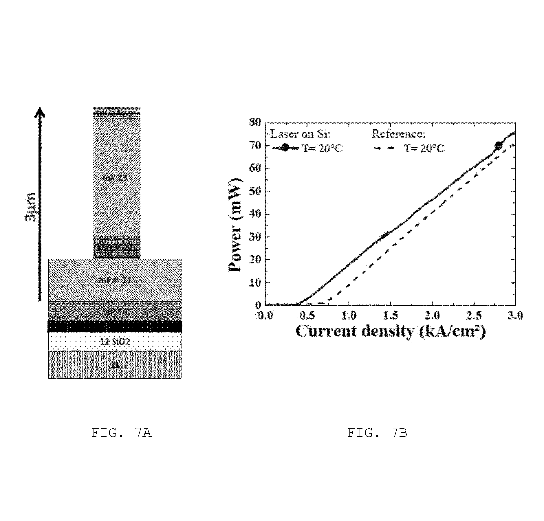
- Figure 7A schematically represents a laser according to the third mode of realization (with a wavelength of 400
- Figure 7B is a graph showing the evolution of the power as a function of current intensity, for the laser shown on Figure
- Figure 1 schematizes a device for regrowth 1 of a thick structure lattice-matched with InP according to some example embodiments. comprising: a silicon (Si) substrate 11, an interface layer of silicon dioxide (Si0 2 ) 12 on the Si substrate 11, a bonding layer 13 made of III-V compound Aluminum Indium
- AlInAs AlInAs
- Figure 2A depicts the first group of steps of this method of fabrication comprising: providing an InP substrate 41; preferably, but not necessarily, layering a stop-etch layer 42 on the InP substrate 41; layering a regrowth layer 14 made of InP on the InP substrate 41 or, where applicable on the stop-etch layer
- the bonding is realized by hydrophilic direct bonding.
- Figure 2B depicts the second group of steps of the method of fabrication according to the third example embodiment, comprising: providing a Si substrate 11; layering the Si substrate with an Si0 2 interface layer
- the bonding is realized by hydrophilic direct bonding.
- Figure 2C depicts the last step of the method of fabrication according to the third example embodiment, corresponding to the removal of the InP substrate 41.
- etching 41 may be realized either by selective chemical etching or by ion implantation followed by splitting and polishing.
- a removal selective chemical etching it is preferable to layer a stop-etch layer 42 on the InP substrate 41, before layering the regrowth layer 14. In that case, a step of removing the stop-etch layer 42 would be realized simultaneously with the removal of the InP substrate 41.
- FIG. 3 are microscopic images (100 ⁇ scale) after annealing under the standard growth conditions on a) a device for regrowth with InP bonding, b) a device for regrowth of a thick structure according to some example embodiments with an AlInAs bonding 13, and c) a device for regrowth of a thick structure according to some example embodiments with an GalnAs bonding 13.
- an InP layer 14 as bonding layer i.e. no bonding layer 13 as depicted by FIG. 3a showing a device for regrowth
- voids or cavities are noticed at the bonding interface (FIG.
- This thick structure 2 comprises, successively from the device for regrowth 1 according to some example embodiments (as depicted by FIG. 1): an inferior cladding 21, comprising at least a first in ⁇
- V material layer at least an active layer 22 on the inferior cladding 21, and on the active layer 22, a superior cladding 23 comprising at least a second III-V material layer.
- This thick structure 2 on the device for regrowth 1 according to the first embodiment constitutes a photonic device 3 according to the some example embodiments, that may include or not a silicon waveguide 120 that is embedded in the interface layer of Si0212 on the Si substrate 11.
- This photonic device 3 may be typically used for emission or detection applications needed into the silicon photonic platform, fully regrown onto silicon.
- a use case is a laser structure 3 which includes a MQW active core
- III-V material and Silicon offers an enhanced durability considering strain stress due to thermal effects, which allows to obtain an increased thickness of the resulting assembly.
- FIG. 5b, 5c, 5d are respectively Scanning Electron transmission Microscopic (STEM) and Atomic Force Microscopic (AFM) images of a photonic device 3 according to the third example embodiment, with a vertical structure 2 grown onto an AlInAs bonding layer 13, for a total thickness of about 3 pm.
- STEM Scanning Electron transmission Microscopic
- AFM Atomic Force Microscopic
- FIG. 6a and 6b show the evolution as a function of wavelength of a photoluminescence (PL) signal on a 2750 nm thick regrown structure of a photonic device according some exemplary embodiments (FIG. 6b), shown next to the schematically adjacent representation of said photonic device (FIG. 6a).
- Figure FIG. 6b clearly shows that the intensity of the photoluminescence (PL) signal is higher if the thick structure 2 has grown on an AlInAs bonding layer 13 than on an InP layer, for each wavelength tested.
- FIG. 7b shows the evolution of the power as a function of current intensity, for a laser device according to some exemplary embodiments, shown next to the schematically adjacent representation of said laser device (FIG. 7a). This figure shows that not only high-material quality has been demonstrated but also a laser effect has been performed based on the same vertical laser- structure with a substantially increased thickness.
Landscapes
- Physics & Mathematics (AREA)
- General Physics & Mathematics (AREA)
- Optics & Photonics (AREA)
- Condensed Matter Physics & Semiconductors (AREA)
- Electromagnetism (AREA)
- Engineering & Computer Science (AREA)
- Microelectronics & Electronic Packaging (AREA)
- Semiconductor Lasers (AREA)
Abstract
A device (1) for regrowth of a thick structure lattice-matched with InP comprising: - a Si substrate (11), - an interface layer of SiO2 (12) on the Si substrate, - a bonding layer (13) on the interface layer (12), said bonding layer (13) being made of a III-V material consisting of an alloy of the AlGalnAs family, and - a regrowth layer (14) on the bonding layer (13), said regrowth layer (14) being made of InP.
Description
DEVICE FOR RBGROWTH OF A THICK STRUCTURE, PHOTONIC DEVICE
COMPRISING THE SAME AND ASSOCIATED METHODS OF FABRICATION
TECHNICAL FIELD [1] Various example embodiments relate to optical components, notably to photonic devices. More particularly, various embodiments relate to the fabrication of thick photonic devices fully regrown onto silicon. BACKGROUND
[2] As known by those skilled in the art, silicon photonics lack efficient light emission and amplification. Thus, the integration of III-V semiconductors on top of silicon waveguide circuits is required to achieve complex integrated circuits. Heterogeneous integration through wafer bonding allows for dense and wafer-scale integration of the III-V optoelectronic components on the silicon photonic platform.
[3] In this wafer bonding approach, there is only one epitaxial step of the full III-V heterostructure which is performed before the bonding step. This allows obtaining best quality III-V material. On the other hand, the epitaxial tool kit is much larger in the conventional III-V industry on adapted III-V wafers. Several and separate epitaxial steps can follow each other, such as selective area growth, butt-joint regrowth, cladding regrowth,
lateral regrowth, most of them used for the so-called "buried heterostructure lasers". Nevertheless, additional processing and epitaxial steps are not possible before wafer bonding. The surface roughness must remain extremely low (RMS below 0.5 nm) to be compatible with bonding requisites. Moreover III/V devices would require a precise alignment at the bonding step in order for each device to be well placed on the top silicon circuits. This alignment might be extremely difficult, is time consuming and could be quite expensive [4] That is why other approaches have been developed by many industrial manufacturers in order to offer a larger epitaxial tool kit to designers of silicon photonic devices.
[5] One of those is to add epitaxial regrowth steps after the bonding step. This implies to make possible the epitaxial regrowth on a III-V bonded seed onto a Si02/Si substrate. This so-called template must be compatible, in terms of coefficient of thermal expansion (GTE) and bonding interface mechanical resistance, with the very high temperature needed during epitaxy.
[6] Regrowth on a directly bonded InP-Si02/Si membrane is a good way to avoid suffering from an InP/Si lattice mismatch and polarity differences as opposed to direct growth on silicon. However, a bonded membrane is exposed to the difference in thermal coefficient between III-V and Si. At a typical epitaxial growth temperature
(610°C-650°C), this difference induces a thermal strain in the growing layer.
[7] Up to now, the thermal strain effects have limited the total regrown thickness achievable while keeping the high level of material quality required for photonic devices. The regrowth of a thick structures (typically from 0.7 pm up to 3 pm) have been investigated. Typically, it has been shown that the photoluminescence signal intensity decreases as the regrown layer thickness increases. Furthermore, the surface roughness RMS (Root
Mean Square) of these structures are in the range of 10 nm, more than ten time higher than on the same structure regrown on an InP substrate. This higher roughness accounts for the lower material quality. By surface roughness RMS, it is meant in the frame of the present application is the Root Mean Square surface roughness average of the profile height deviations from the mean line, recorded within the evaluation length.
[8] Until now, the total thickness of the grown material, whether it is Multiple Quantum Well (MQW) active layers or lateral confinement layers, is limited to typically a half micron. This thickness limitation directly impacts the achievable laser designs and has largely encouraged the "membrane buried heterostructure laser " technique where a thin MQW stack is laterally buried in order to form a p-i-n lateral junction instead of a thick vertical p-i-n junction.
[9] Despite the demonstration of high material quality and component performances, this thickness limitation directly impacts the achievable laser designs used in the conventional InP platform know-how, based on a thick vertical p-i-n junction.
. It is needed to overcome these difficulties of the effects of thermally induced stress and the small total thickness of III-V material.
SUMMARY
[10] Example embodiments of the invention aims to remedy all or some of the disadvantages of the above identified prior art.
[11] The embodiments and features, if any, described in this specification that do not fall under the scope of the independent claims are to be interpreted as examples useful for understanding various embodiments of the invention.
[12] A first example embodiment relates then to a device for regrowth of a thick structure lattice-matched with InP comprising: a Si substrate, an interface layer of Si02 on the Si substrate, a bonding layer on the interface layer, said bonding layer being made of a III-V material consisting of an alloy of the AlGalnAs material family. a regrowth layer on the bonding layer, said regrowth layer being made of InP.
[13] By alloy of the AlGalnAs material family, it is meant, in the present application, components comprising As and at least two elements chosen among of the group consisting of Al, Ga, and In.
[14] The device for regrowth according to the first example embodiment offers a way to put up with the effects of thermally induced stress and to allows the regrowth of a thick structure of
III-V material lattice-matched with InP, by using a specific Ill-
V material at the bonding interface with Si02/Si, which offers a higher bonding strength. This enables to further increase the total thickness of III-V material.
[15] Advantageously, the interface layer of Si02 may comprise a silicon waveguide.
[16] Advantageously, the bonding layer AlGalnAs composition/material family is chosen to obtain an almost perfect lattice match with InP lattice parameter (with a tolerance usually better than 0.1% and typically around 0.01% or 100 PPM).
[17] Advantageously, we can use an alloy (AlzGai-z)xIni-xAs with 0 ≤ z ≤ 1 and 0.465 ≤ x ≤ 0.481, lattice matched to InP.
[18] Advantageously, the bonding layer may consist of GalnAs which has the advantage to form a stable interface with a thermal Si02.
Prefarably, we can use an alloy GaxIni-xAs with 0.465 ≤ x ≤ 0.481 lattice matched to InP.
[19] Advantageously, the bonding layer may consist of AlInAs which has the advantage that the material formed at the interface
resulting from the reaction between AlInAs and thermal SiO2 has a very high stability. Advantageously, we can use an alloy AlxIm-xAs with 0.465 ≤ x ≤ 0.481 lattice matched to InP.
[20] In particular, a device comprising a bonding layer on the interface layer consisting in an InP/AlInAs (lOnm)-bonded-to- SiO2 Si(substrate) stack offers a strong adherence which permits the bonding structure to resist an important strain energy due to the thermal coefficient expansion (GTE) mismatch and a thick regrowth. The thicker the structure in regrowth, the higher chance of an evolution of the bonding interface due to the thermal strain energy. This InP/AlInAs(lOnm)-bonded-to-Si02/Si(sub) may serve for all kind of support for regrowth of a thick structure lattice- matched with InP. More particularly, for telecom-oriented applications, a 3μm-thick vertical p-i-n junction, both for emission or reception, may be regrown, including cladding, active, contact layers.
[21] Advantageously, the thickness of the bonding layer may be comprised between 1 and 100 nm, preferably between 5 and 50 nm, and even more preferably between 8 and 12 nm.
[22] Advantageously, the thickness of the regrowth layer being made of InP may be of about 100 nm.
[23] A second example embodiment relates to a photonic device for combining a silicon "Si" material and a III-V material comprising:
the device for regrowth of a thick structure lattice- matched with InP according to the first example embodiment, an inferior cladding on the regrowth layer of the device for regrowth according to the first example embodiment, said inferior cladding comprising at least one III-V material layer, at least an active layer on the inferior cladding, a superior cladding on the active layer, said superior cladding comprising at least one III-V material layer.
[24] The first and second III-V materials may be same or different.
[25] Advantageously, the active layer may be a Multiple Quantum
Well layer. In that case, the photonic device may be used as a light tuning device, such as optical waveguide, laser, modulator or optical amplifier.
[26] Advantageously, the active layer may be a thick absorption layer. In that case, the photonic device may be used as a light detector device.
[27] Advantageously the surface roughness RMS of the superior cladding may be less than 1 nanometer.
[28] Advantageously the total thickness of the inferior cladding, the active layer, and the superior cladding may be higher than 1 pm, and preferably of about 3 pm.
[29] Advantageously, the total thickness of the first III-V material layer, the active layer, the second III-V material layer and the third III-V material layer is higher than 1 micron, and preferably about 3 microns.
[30] A third example embodiment relates to a method of fabrication of a device for regrowth of a thick structure lattice-matched with
InP comprising the following steps: providing a Si substrate; layering the Si substrate with an Si02 interface layer by thermal oxidation of said Si substrate; providing an InP substrate; layering a regrowth layer made of InP on the InP substrate; layering a bonding layer made of an alloy of the(AlGa)InAs family on the regrowth layer, by epitaxial growth so as to form a stack; bonding the SiO2 interface layer and the bonding layer of the stack; removing the InP substrate.
[31] Advantageously, the step of bonding the SiO2 interface layer and the bonding layer of the stack may be realized by hydrophilic direct bonding.
[32] Advantageously, the method of fabrication of a device for regrowth of a thick structure lattice-matched according to the third example embodiment may further comprise the following steps:
• between the steps of providing an InP substrate and the step of layering a regrowth layer made of InP, a step of layering a stop-etch layer on the InP substrate; and
• a step of removing the stop-etch layer that is realized simultaneously with removal of the InP substrate.
[33] In that case, the step of removing the stop-etch layer and the InP substrate may be preferably realized by chemical selective etching.
[34] Advantageously, the substrate might be partially removed using a grinding step to minimize the amount of InP substrate material removed by chemical selective etching.
[35] A fourth example embodiment relates to a method for growing a semiconductor heterogeneous structure on a Si substrate comprising the following steps: providing a device for regrowth of a thick structure lattice-matched with InP according to the first embodiment, or fabricated according to the method of fabrication of the fourth embodiment; growing at least a first III-V material layer on the regrowth layer of said device for regrowth, so as to form an inferior cladding,
growing an active layer on the inferior cladding, growing at least a second III-V material layer on the active layer, so as to form a superior cladding; growing a third III-V material layer on the superior cladding.
[36] Advantageously, the step of growing the inferior cladding on the regrowth layer, the step of growing the active layer on the inferior cladding, and the step of growing the superior cladding on the active layer may be realized by Metalorganic Vapor Phase
Epitaxy (MOVPE or equivalently organometallic vapor-phase epitaxy
OMVPE) growth or by Molecular Beam Epitaxy growth.
[37] Advantageously, the method for growing a semiconductor heterogeneous structure on a Si substrate according to the fourth example embodiment may comprise the following features: the inferior cladding layer is made of InP, the active layer is a Multiple Quantum Well layer, the superior cladding is made of InP, the second III-V material layer on top of the superior cladding is made of GalnAs.
BRIEF DESCRIPTION OF THE DRAWINGS
[38] Some example embodiments are now described, by way of example only, and with reference to the accompanying drawings in which:
FIG. 1 schematically represents a device for regrowth of a thick structure lattice-matched with InP according to some example embodiments;
FIG. 2A to 2C schematically depict the different steps of a method of fabrication of a device for regrowth of a thick structure lattice-matched with InP according to some example embodiments;
FIG. 3 are microscopic images after annealing under the standard growth conditions on a) a device for regrowth (InP bonding), b) a device for regrowth of a thick structure according to some example embodiments with an AlInAs bonding, and c) a device for regrowth of a thick structure according to some example embodiments with an GalnAs bonding;
FIG. 4A and FIG. 4B schematically represent a photonic device for, respectively on Si02/Si and on Si02/Si waveguide/Si, for combining a silicon "Si" material and a III-V material according to some example embodiments;
FIG. 5 are Scanning Electron transmission Microscopic (STEM) and Atomic Force Microscopic (AFM) images of a photonic device according to some example embodiments, with a vertical structure grown onto a bonded seed for a total thickness of about 3 μm;
Figure 6a schematically represents a photonic device according to some example embodiment presenting a 2750 nm thick regrown structure and Figure 6B is a graph showing the evolution as a function of wavelength of a photoluminescence
(PL) signal on the thick regrown structure of the photonic device shown on figure 6A ;
Figure 7A schematically represents a laser according to the third mode of realization (with a wavelength of 400 |im), and
Figure 7B is a graph showing the evolution of the power as a function of current intensity, for the laser shown on Figure
7A.
[39] The same reference number represents the same element or the same type of element on all drawings, unless stated otherwise. DBTAILLBD DESCRIPTION
[40] The figures and the following description illustrate specific exemplary embodiments of the invention. It will thus be appreciated that those skilled in the art will be able to devise various arrangements that, although not explicitly described or shown herein, embody the principles of the invention and are included within the scope of the invention. Furthermore, any examples described herein are intended to aid in understanding the principles of the invention, and are to be construed as being
without limitation to such specifically recited examples and conditions. As a result, the invention is not limited to the specific embodiments or examples described below, but by the claims and their equivalents.
[41] In the following description, well-known functions or constructions by the man skilled in the art are not described in detail since they would obscure the invention in unnecessary detail.
[42] In the following description of the figures, schematic representations are non-limiting and serve only for the understanding of the invention.
[43] Figure 1 schematizes a device for regrowth 1 of a thick structure lattice-matched with InP according to some example embodiments. comprising: a silicon (Si) substrate 11, an interface layer of silicon dioxide (Si02) 12 on the Si substrate 11, a bonding layer 13 made of III-V compound Aluminum Indium
Arsenide (AlInAs) or III-V compound Indium Gallium Arsenide
(GalnAs) on the interface layer 12, and a regrowth layer 14 made of Indium Phosphide (InP) on the bonding layer 13.
[44] The device for regrowth 1 shown on figure 1 is obtained by a method of fabrication according to the third example embodiment,
the different steps of which are schematically depicted by Figures
2A to 2C.
[45] In particular, Figure 2A depicts the first group of steps of this method of fabrication comprising: providing an InP substrate 41; preferably, but not necessarily, layering a stop-etch layer 42 on the InP substrate 41; layering a regrowth layer 14 made of InP on the InP substrate 41 or, where applicable on the stop-etch layer
42; layering a bonding layer 13 made of AlInAs or GalnAs on the regrowth layer 14, by epitaxial growth in an example, so as to form a stack 4.
[46] Advantageously the bonding is realized by hydrophilic direct bonding.
[47] Figure 2B depicts the second group of steps of the method of fabrication according to the third example embodiment, comprising: providing a Si substrate 11; layering the Si substrate with an Si02 interface layer
12 by thermal oxidation of said Si substrate 11, preferably at a temperature between 800°C and 1250°C
(notably at 950 or 1050°C on silicon with a dry oxygen or wet atmosphere);
bonding the SiO2 interface layer 12 and the bonding layer
13 of the stack 4 (more preciously the bonding layer
13).
[48] Advantageously the bonding is realized by hydrophilic direct bonding.
[49] Figure 2C depicts the last step of the method of fabrication according to the third example embodiment, corresponding to the removal of the InP substrate 41. The removal of the InP substrate
41 may be realized either by selective chemical etching or by ion implantation followed by splitting and polishing. In the case of a removal selective chemical etching, it is preferable to layer a stop-etch layer 42 on the InP substrate 41, before layering the regrowth layer 14. In that case, a step of removing the stop-etch layer 42 would be realized simultaneously with the removal of the InP substrate 41.
[50] FIG. 3 are microscopic images (100 μπι scale) after annealing under the standard growth conditions on a) a device for regrowth with InP bonding, b) a device for regrowth of a thick structure according to some example embodiments with an AlInAs bonding 13, and c) a device for regrowth of a thick structure according to some example embodiments with an GalnAs bonding 13. In particular, in the case of an InP layer 14 as bonding layer (i.e. no bonding layer 13 as depicted by FIG. 3a showing a device for regrowth, voids or cavities are noticed at the bonding interface (FIG. 3a)
whereas, thanks to exemplary embodiments, in the case of an intermediate AlInAs bonding layer 13 (FIG. 3b) or an GalnAs bonding layer 13 (FIG 3c) formed between the interface Si02 layer 12 and the InP regrowth layer 14, a thermally stable material is formed at the interface from the reaction between AlInAs (respectively
GalnAs) and the thermal Si02.
[51] Since both GalnAs and AlInAs bonding layers 13 at the bonding interface show thermal stability during annealing, an epitaxial regrowth of thick structure (of about 1 to 3 pm) is achievable, as schematically depicted by Figure 4. This thick structure 2 comprises, successively from the device for regrowth 1 according to some example embodiments (as depicted by FIG. 1): an inferior cladding 21, comprising at least a first in ¬
V material layer, at least an active layer 22 on the inferior cladding 21, and on the active layer 22, a superior cladding 23 comprising at least a second III-V material layer.
[52] This thick structure 2 on the device for regrowth 1 according to the first embodiment constitutes a photonic device 3 according to the some example embodiments, that may include or not a silicon waveguide 120 that is embedded in the interface layer of Si0212 on the Si substrate 11. This photonic device 3 may be typically used for emission or detection applications needed into the silicon
photonic platform, fully regrown onto silicon. The III-V material family materials of the inferior cladding 21 and superior cladding
23 match the InP lattice parameters and is fully regrown onto a specific InP-AlGalnAs thin structure previously bonded onto Si02/Si
(device for regrowth 1). Best results in terms of seed material quality can be obtained with a 10 nm thick AlInAs layer followed by an InP buffer layer onto a thermal silica formed on silicon. A use case is a laser structure 3 which includes a MQW active core
22 surrounded by n type 21 and p type 23 thick claddings for a total thickness of substantially 3 pm (Figures 5 to 7).
Advantageously, the combination of AlGalnAs bonding layer with
III-V material and Silicon offers an enhanced durability considering strain stress due to thermal effects, which allows to obtain an increased thickness of the resulting assembly.
[53] Material-related characterizations have been done on the structure 2 grown onto an AlInAs bonding layer 13.
[54] Thus FIG. 5b, 5c, 5d are respectively Scanning Electron transmission Microscopic (STEM) and Atomic Force Microscopic (AFM) images of a photonic device 3 according to the third example embodiment, with a vertical structure 2 grown onto an AlInAs bonding layer 13, for a total thickness of about 3 pm.
Advantageously, the STEM analysis does not show any trace of dislocations and the mean roughness is less than lnm (FIG 5c).
[55] Figure FIG. 6a and 6b show the evolution as a function of wavelength of a photoluminescence (PL) signal on a 2750 nm thick regrown structure of a photonic device according some exemplary embodiments (FIG. 6b), shown next to the schematically adjacent representation of said photonic device (FIG. 6a). Figure FIG. 6b clearly shows that the intensity of the photoluminescence (PL) signal is higher if the thick structure 2 has grown on an AlInAs bonding layer 13 than on an InP layer, for each wavelength tested.
[56] Figure FIG. 7b shows the evolution of the power as a function of current intensity, for a laser device according to some exemplary embodiments, shown next to the schematically adjacent representation of said laser device (FIG. 7a). This figure shows that not only high-material quality has been demonstrated but also a laser effect has been performed based on the same vertical laser- structure with a substantially increased thickness.
Claims
1- A device for regrowth (1) of a thick structure lattice-matched with InP comprising: a Si substrate (11), an interface layer of SiO2 (12) on the Si substrate (11), a bonding layer (13) on the interface layer (12), said bonding layer (13) being made of a III-V material consisting of an alloy of the AlGalnAs family, and a regrowth layer (14) on the bonding layer, said regrowth layer being made of InP.
2. A device (1) according to claim 1, where the interface layer
(12) of Si02 comprises a silicone waveguide (120).
3. A device according to claims 1 or 2, where the bonding layer
(13) is made of AlInAs.
4. A device according to anyone of claims 1 to 3, where the thickness of the bonding layer (13) is comprised between substantially 1 and substantially 100 nm, and preferably between substantially 5 and substantially 50 nm.
25
5. A photonic device (3) for combining a silicon "Si" material and a III-V material comprising: a device for regrowth (1) of a thick structure (2) lattice- matched with InP according to any of the claims 1 to 4, an inferior cladding (21) on the regrowth layer (14) of said device for regrowth (1), said inferior cladding (21) comprising at least a first III-V material layer, at least an active layer (22) on the inferior cladding (21), a superior cladding (23) on the active layer (22), said superior cladding (23) comprising at least a second III-V material layer.
6. A photonic device (3) according to claim 5, wherein the active layer (22) is a Multiple Quantum Well layer.
7. A photonic device (3) according to claim 5, wherein the active layer (22) is a thick absorbent layer.
8. A photonic device (3) according to claim 7, where the surface roughness of the superior cladding (23) is less than 1 nanometer.
9. A photonic device (3) according to claim 7 or 8, where the total thickness of the inferior cladding (21), the active layer (22),
and the superior cladding (23) is higher than 1 μm, and preferably about 3 pm.
10. A method of fabrication of a device (1) for regrowth of a thick structure (2) lattice-matched with InP comprising the following steps: providing a Si substrate (11); layering the Si substrate with an SiO22 interface layer (12) by thermal oxidation of said Si substrate (11); providing an InP substrate (41); layering a regrowth layer (14) made of InP on the InP substrate (41); layering a bonding layer (13) made of an alloy of the AlGalnAs family on the regrowth layer (14), by epitaxial growth so as to form a stack (4); bonding the SiO2 interface layer (12) and the bonding layer
(13) of the stack (4); removing the InP substrate (41).
11. A method of fabrication according to claims 10, wherein the step of bonding the SiO2 interface layer (12) and the bonding layer
(13) of the stack (4) is realized by hydrophilic molecular bonding.
12. A method of fabrication according to claims 10 or 11, further comprising the following steps:
• between the steps of providing an InP substrate (41) and the step of layering a regrowth layer made of InP (14), a step of layering a stop-etch layer (42) on the InP substrate (41); and
• a step of removing the stop-etch layer (42) that is realized substantially simultaneously with the step of removing of the
InP substrate (41).
13. A method of fabrication according to claim 12, where the step of removing the stop-etch layer (42) and the InP substrate (41) is realized by chemical selective etching.
14. A method for growing a semiconductor heterogeneous structure on a Si substrate (11) comprising the following steps:
• providing a device for regrowth (1) of a thick structure (2) lattice-matched with InP as defined in any of the claims 1 to
4, or fabricated according to the method of fabrication according to any of the claims 10 to 13,
• growing at least a first III-V material layer on the regrowth layer (14) of said device for regrowth (1), so as to form an inferior cladding (21),
• growing an active layer (22) on the inferior cladding (21),
• growing at least a second III-V material layer on the active layer (22), so as to form a superior cladding (23),
• growing a third III-V material layer (24) on the superior cladding (23).
15. A method for growing a semiconductor heterogeneous structure on a "Si" substrate according to claim 14, wherein:
• the inferior cladding layer (21) is made of InP,
• the active layer (22) is a Multiple Quantum Well layer,
• the superior cladding (23) is made of InP.
• the second III-V material layer (24) on top of the superior cladding (23) is made of GalnAs.


Priority Applications (1)
| Application Number | Priority Date | Filing Date | Title |
|---|---|---|---|
| US17/769,153 US20240113493A1 (en) | 2019-10-16 | 2020-10-15 | Device for regrowth of a thick structure, photonic device comprising the same and associated methods of fabrication |
Applications Claiming Priority (2)
| Application Number | Priority Date | Filing Date | Title |
|---|---|---|---|
| EP19315126.3A EP3809540A1 (en) | 2019-10-16 | 2019-10-16 | Device for regrowth of a thick structure, photonic device comprising the same and associated methods of fabrication |
| EP19315126.3 | 2019-10-16 |
Publications (1)
| Publication Number | Publication Date |
|---|---|
| WO2021074331A1 true WO2021074331A1 (en) | 2021-04-22 |
Family
ID=68762681
Family Applications (1)
| Application Number | Title | Priority Date | Filing Date |
|---|---|---|---|
| PCT/EP2020/079114 Ceased WO2021074331A1 (en) | 2019-10-16 | 2020-10-15 | Device for regrowth of a thick structure, photonic device comprising the same and associated methods of fabrication |
Country Status (3)
| Country | Link |
|---|---|
| US (1) | US20240113493A1 (en) |
| EP (1) | EP3809540A1 (en) |
| WO (1) | WO2021074331A1 (en) |
Families Citing this family (1)
| Publication number | Priority date | Publication date | Assignee | Title |
|---|---|---|---|---|
| CN121566267A (en) * | 2026-01-23 | 2026-02-24 | 江西兆驰集成科技有限公司 | Silicon-based indium phosphide laser and preparation method thereof |
Citations (1)
| Publication number | Priority date | Publication date | Assignee | Title |
|---|---|---|---|---|
| US20160087160A1 (en) * | 2014-09-22 | 2016-03-24 | International Business Machines Corporation | Iii-v photonic integrated circuits on silicon substrate |
Family Cites Families (9)
| Publication number | Priority date | Publication date | Assignee | Title |
|---|---|---|---|---|
| US7019332B2 (en) * | 2001-07-20 | 2006-03-28 | Freescale Semiconductor, Inc. | Fabrication of a wavelength locker within a semiconductor structure |
| EP1429160A4 (en) * | 2001-09-19 | 2005-09-14 | Matsushita Electric Industrial Co Ltd | OPTICAL WAVEGUIDE AND METHOD OF MANUFACTURING THE SAME |
| US7119377B2 (en) * | 2004-06-18 | 2006-10-10 | 3M Innovative Properties Company | II-VI/III-V layered construction on InP substrate |
| US8692260B2 (en) * | 2008-09-26 | 2014-04-08 | Soitec | Method of forming a composite laser substrate |
| KR20150012525A (en) * | 2013-07-25 | 2015-02-04 | 한국전자통신연구원 | optical devices and manufacturing method of the same |
| US9922830B2 (en) * | 2014-04-07 | 2018-03-20 | International Business Machines Corporation | Hybrid III-V technology to support multiple supply voltages and off state currents on same chip |
| US10340661B2 (en) * | 2017-11-01 | 2019-07-02 | International Business Machines Corporation | Electro-optical device with lateral current injection regions |
| WO2019220207A1 (en) * | 2018-05-16 | 2019-11-21 | Rockley Photonics Limited | lll-V/SI HYBRID OPTOELECTRONIC DEVICE AND METHOD OF MANUFACTURE |
| GB2586889B (en) * | 2019-08-26 | 2022-11-02 | Rockley Photonics Ltd | Method of manufacturing a III-V based optoelectronic device |
-
2019
- 2019-10-16 EP EP19315126.3A patent/EP3809540A1/en active Pending
-
2020
- 2020-10-15 WO PCT/EP2020/079114 patent/WO2021074331A1/en not_active Ceased
- 2020-10-15 US US17/769,153 patent/US20240113493A1/en active Pending
Patent Citations (1)
| Publication number | Priority date | Publication date | Assignee | Title |
|---|---|---|---|---|
| US20160087160A1 (en) * | 2014-09-22 | 2016-03-24 | International Business Machines Corporation | Iii-v photonic integrated circuits on silicon substrate |
Non-Patent Citations (4)
| Title |
|---|
| BESANCON CLAIRE ET AL: "High-quality Epitaxial Growth of AlGaInAs-based Active Structure on a Directly-Bonded InPoSi Substrate", 2019 COMPOUND SEMICONDUCTOR WEEK (CSW), IEEE, 19 May 2019 (2019-05-19), pages 1 - 2, XP033609581, DOI: 10.1109/ICIPRM.2019.8818994 * |
| FANG A W ET AL: "Electrically pumped hybrid AlGaInAs-silicon evanescent laser", OPTICS EXPRESS, OSA PUBLISHING, US, vol. 14, no. 20, 2 October 2006 (2006-10-02), pages 9203 - 9210, XP002457693, ISSN: 1094-4087, DOI: 10.1364/OE.14.009203 * |
| MICHAEL L. DAVENPORT ET AL: "Heterogeneous Silicon/III-V Semiconductor Optical Amplifiers", IEEE JOURNAL OF SELECTED TOPICS IN QUANTUM ELECTRONICS., vol. 22, no. 6, 1 November 2016 (2016-11-01), US, pages 78 - 88, XP055682705, ISSN: 1077-260X, DOI: 10.1109/JSTQE.2016.2593103 * |
| SHINJI MATSUO ET AL: "Directly modulated buried heterostructure DFB laser on SiO_2/Si substrate fabricated by regrowth of InP using bonded active layer", OPTICS EXPRESS, vol. 22, no. 10, 12 May 2014 (2014-05-12), pages 12139, XP055682725, DOI: 10.1364/OE.22.012139 * |
Also Published As
| Publication number | Publication date |
|---|---|
| US20240113493A1 (en) | 2024-04-04 |
| EP3809540A1 (en) | 2021-04-21 |
Similar Documents
| Publication | Publication Date | Title |
|---|---|---|
| US11550099B2 (en) | Photonics optoelectrical system | |
| JP5006876B2 (en) | Quantum dot based optoelectronic device and method of making the same | |
| Mauthe et al. | InP-on-Si optically pumped microdisk lasers via monolithic growth and wafer bonding | |
| EP2214042A1 (en) | Method of producing a photonic device and corresponding photonic device | |
| JP2010263153A (en) | Semiconductor integrated optical device and manufacturing method thereof | |
| US12366705B2 (en) | Photonics optoelectrical system | |
| US20140016659A1 (en) | Semiconductor Device and Fabrication Method | |
| JP4260480B2 (en) | Method of manufacturing an optical device and related improvements | |
| Kunert et al. | Application of an sb surfactant in InGaAs nano-ridge engineering on 300 mm silicon substrates | |
| CN104205362A (en) | Fabrication of multi-junction solar cell devices | |
| US20240113493A1 (en) | Device for regrowth of a thick structure, photonic device comprising the same and associated methods of fabrication | |
| US9859685B2 (en) | Small aperture formation for facilitating optoelectronic device integration with defective semiconductor materials | |
| JP2004523120A (en) | Semiconductor laser with multiple optically active regions | |
| Bordel et al. | Direct and polymer bonding of III-V to processed silicon-on-insulator for hybrid silicon evanescent lasers fabrication | |
| JP7540048B1 (en) | Heterogeneous integrated photonic platform with InGaP layers | |
| Hu et al. | Electrically-pumped 1.31 μm MQW lasers by direct epitaxy on wafer-bonded InP-on-SOI substrate | |
| Kuhlow et al. | Photonic crystal microcavities in SOI photonic wires for WDM filter applications | |
| US6261855B1 (en) | Method for fabricating a semiconductor optical device | |
| JP2004527106A (en) | Method of manufacturing an optical device and related improvements | |
| US20020127758A1 (en) | Method of efficient controllable and repeatable wet oxidation in a phosphorous-rich III-V material system | |
| Fujii et al. | Heterogeneously integrated lasers using epitaxially grown III-V active layer on directly bonded InP/SiO 2/Si substrate | |
| EP4641644A1 (en) | Layered semiconductor structure and method of fabricating layered semiconductor structure | |
| JP2956668B2 (en) | Semiconductor laser | |
| JP3218582B2 (en) | GaInAs photodiode | |
| Bakir et al. | Electrically driven hybrid Si/III-V lasers based on adiabatic mode transformers |
Legal Events
| Date | Code | Title | Description |
|---|---|---|---|
| 121 | Ep: the epo has been informed by wipo that ep was designated in this application |
Ref document number: 20790308 Country of ref document: EP Kind code of ref document: A1 |
|
| WWE | Wipo information: entry into national phase |
Ref document number: 17769153 Country of ref document: US |
|
| NENP | Non-entry into the national phase |
Ref country code: DE |
|
| 122 | Ep: pct application non-entry in european phase |
Ref document number: 20790308 Country of ref document: EP Kind code of ref document: A1 |