WO2021069595A1 - Compound and an organic semiconducting layer, an organic electronic device, a display device and a lighting device comprising the same - Google Patents
Compound and an organic semiconducting layer, an organic electronic device, a display device and a lighting device comprising the same Download PDFInfo
- Publication number
- WO2021069595A1 WO2021069595A1 PCT/EP2020/078287 EP2020078287W WO2021069595A1 WO 2021069595 A1 WO2021069595 A1 WO 2021069595A1 EP 2020078287 W EP2020078287 W EP 2020078287W WO 2021069595 A1 WO2021069595 A1 WO 2021069595A1
- Authority
- WO
- WIPO (PCT)
- Prior art keywords
- partially
- group
- alkyl
- formula
- alkoxy
- Prior art date
Links
- 150000001875 compounds Chemical class 0.000 title claims abstract description 122
- 125000004432 carbon atom Chemical group C* 0.000 claims description 131
- 125000003545 alkoxy group Chemical group 0.000 claims description 91
- 125000003187 heptyl group Chemical group [H]C([*])([H])C([H])([H])C([H])([H])C([H])([H])C([H])([H])C([H])([H])C([H])([H])[H] 0.000 claims description 61
- 125000000217 alkyl group Chemical group 0.000 claims description 52
- 125000003118 aryl group Chemical group 0.000 claims description 52
- -1 azaphenanthrenyl Chemical group 0.000 claims description 49
- 125000001997 phenyl group Chemical class [H]C1=C([H])C([H])=C(*)C([H])=C1[H] 0.000 claims description 41
- 125000001424 substituent group Chemical group 0.000 claims description 33
- 229910052731 fluorine Inorganic materials 0.000 claims description 32
- 229910052799 carbon Inorganic materials 0.000 claims description 25
- 239000002019 doping agent Substances 0.000 claims description 25
- 125000004433 nitrogen atom Chemical group N* 0.000 claims description 18
- 125000001072 heteroaryl group Chemical group 0.000 claims description 16
- 229910052739 hydrogen Inorganic materials 0.000 claims description 15
- 125000001624 naphthyl group Chemical group 0.000 claims description 12
- 239000000654 additive Substances 0.000 claims description 10
- 125000005549 heteroarylene group Chemical group 0.000 claims description 8
- YNPNZTXNASCQKK-UHFFFAOYSA-N phenanthrene Chemical compound C1=CC=C2C3=CC=CC=C3C=CC2=C1 YNPNZTXNASCQKK-UHFFFAOYSA-N 0.000 claims description 8
- 230000000996 additive effect Effects 0.000 claims description 7
- 125000004076 pyridyl group Chemical group 0.000 claims description 7
- 125000000609 carbazolyl group Chemical group C1(=CC=CC=2C3=CC=CC=C3NC12)* 0.000 claims description 4
- 125000002183 isoquinolinyl group Chemical group C1(=NC=CC2=CC=CC=C12)* 0.000 claims description 4
- 125000002943 quinolinyl group Chemical group N1=C(C=CC2=CC=CC=C12)* 0.000 claims description 4
- 125000005550 pyrazinylene group Chemical group 0.000 claims description 2
- 125000005576 pyrimidinylene group Chemical group 0.000 claims description 2
- 125000001567 quinoxalinyl group Chemical group N1=C(C=NC2=CC=CC=C12)* 0.000 claims description 2
- 125000005558 triazinylene group Chemical group 0.000 claims description 2
- 239000010410 layer Substances 0.000 description 323
- 230000000903 blocking effect Effects 0.000 description 37
- 238000002347 injection Methods 0.000 description 36
- 239000007924 injection Substances 0.000 description 36
- VLKZOEOYAKHREP-UHFFFAOYSA-N n-Hexane Chemical compound CCCCCC VLKZOEOYAKHREP-UHFFFAOYSA-N 0.000 description 36
- 238000000151 deposition Methods 0.000 description 34
- YMWUJEATGCHHMB-UHFFFAOYSA-N Dichloromethane Chemical compound ClCCl YMWUJEATGCHHMB-UHFFFAOYSA-N 0.000 description 30
- 230000008021 deposition Effects 0.000 description 29
- 239000000758 substrate Substances 0.000 description 29
- OKKJLVBELUTLKV-UHFFFAOYSA-N Methanol Chemical compound OC OKKJLVBELUTLKV-UHFFFAOYSA-N 0.000 description 27
- 230000005525 hole transport Effects 0.000 description 25
- YXFVVABEGXRONW-UHFFFAOYSA-N Toluene Chemical compound CC1=CC=CC=C1 YXFVVABEGXRONW-UHFFFAOYSA-N 0.000 description 24
- 239000011777 magnesium Substances 0.000 description 19
- ZUOUZKKEUPVFJK-UHFFFAOYSA-N diphenyl Chemical compound C1=CC=CC=C1C1=CC=CC=C1 ZUOUZKKEUPVFJK-UHFFFAOYSA-N 0.000 description 18
- FIDRAVVQGKNYQK-UHFFFAOYSA-N 1,2,3,4-tetrahydrotriazine Chemical compound C1NNNC=C1 FIDRAVVQGKNYQK-UHFFFAOYSA-N 0.000 description 16
- IJGRMHOSHXDMSA-UHFFFAOYSA-N Atomic nitrogen Chemical compound N#N IJGRMHOSHXDMSA-UHFFFAOYSA-N 0.000 description 16
- 239000000463 material Substances 0.000 description 16
- 229910052757 nitrogen Inorganic materials 0.000 description 15
- 239000011159 matrix material Substances 0.000 description 14
- 229910052751 metal Inorganic materials 0.000 description 14
- 239000002184 metal Substances 0.000 description 14
- XLYOFNOQVPJJNP-UHFFFAOYSA-N water Substances O XLYOFNOQVPJJNP-UHFFFAOYSA-N 0.000 description 13
- 229910052784 alkaline earth metal Inorganic materials 0.000 description 11
- 239000011248 coating agent Substances 0.000 description 11
- 238000000576 coating method Methods 0.000 description 11
- 125000001183 hydrocarbyl group Chemical group 0.000 description 11
- 238000000034 method Methods 0.000 description 11
- 239000002904 solvent Substances 0.000 description 11
- 239000004305 biphenyl Substances 0.000 description 10
- 238000004770 highest occupied molecular orbital Methods 0.000 description 10
- 235000010290 biphenyl Nutrition 0.000 description 9
- 239000011575 calcium Substances 0.000 description 9
- 238000004768 lowest unoccupied molecular orbital Methods 0.000 description 9
- 239000000203 mixture Substances 0.000 description 9
- 239000002244 precipitate Substances 0.000 description 9
- 239000007787 solid Substances 0.000 description 9
- 238000004528 spin coating Methods 0.000 description 9
- 238000001771 vacuum deposition Methods 0.000 description 9
- JUJWROOIHBZHMG-UHFFFAOYSA-N Pyridine Chemical compound C1=CC=NC=C1 JUJWROOIHBZHMG-UHFFFAOYSA-N 0.000 description 8
- 229910052749 magnesium Inorganic materials 0.000 description 8
- 239000011541 reaction mixture Substances 0.000 description 8
- 238000001035 drying Methods 0.000 description 7
- 125000005842 heteroatom Chemical group 0.000 description 7
- 239000012299 nitrogen atmosphere Substances 0.000 description 7
- 239000000126 substance Substances 0.000 description 7
- 229910052769 Ytterbium Inorganic materials 0.000 description 6
- 239000003513 alkali Substances 0.000 description 6
- 150000001342 alkaline earth metals Chemical class 0.000 description 6
- 229910052791 calcium Inorganic materials 0.000 description 6
- 239000003795 chemical substances by application Substances 0.000 description 6
- 230000000052 comparative effect Effects 0.000 description 6
- 239000000306 component Substances 0.000 description 6
- 238000004128 high performance liquid chromatography Methods 0.000 description 6
- 238000007639 printing Methods 0.000 description 6
- 229910052783 alkali metal Inorganic materials 0.000 description 5
- 150000001340 alkali metals Chemical class 0.000 description 5
- 125000000732 arylene group Chemical group 0.000 description 5
- 125000004429 atom Chemical group 0.000 description 5
- 230000015572 biosynthetic process Effects 0.000 description 5
- 238000005266 casting Methods 0.000 description 5
- 238000001816 cooling Methods 0.000 description 5
- 125000006575 electron-withdrawing group Chemical group 0.000 description 5
- KDLHZDBZIXYQEI-UHFFFAOYSA-N palladium Substances [Pd] KDLHZDBZIXYQEI-UHFFFAOYSA-N 0.000 description 5
- VYPSYNLAJGMNEJ-UHFFFAOYSA-N silicon dioxide Inorganic materials O=[Si]=O VYPSYNLAJGMNEJ-UHFFFAOYSA-N 0.000 description 5
- 238000007764 slot die coating Methods 0.000 description 5
- 229910052693 Europium Inorganic materials 0.000 description 4
- KFZMGEQAYNKOFK-UHFFFAOYSA-N Isopropanol Chemical compound CC(C)O KFZMGEQAYNKOFK-UHFFFAOYSA-N 0.000 description 4
- 229910052782 aluminium Inorganic materials 0.000 description 4
- XAGFODPZIPBFFR-UHFFFAOYSA-N aluminium Chemical compound [Al] XAGFODPZIPBFFR-UHFFFAOYSA-N 0.000 description 4
- MWPLVEDNUUSJAV-UHFFFAOYSA-N anthracene Chemical compound C1=CC=CC2=CC3=CC=CC=C3C=C21 MWPLVEDNUUSJAV-UHFFFAOYSA-N 0.000 description 4
- 229910052792 caesium Inorganic materials 0.000 description 4
- 239000012043 crude product Substances 0.000 description 4
- 230000000694 effects Effects 0.000 description 4
- 238000000295 emission spectrum Methods 0.000 description 4
- 238000001704 evaporation Methods 0.000 description 4
- 230000008020 evaporation Effects 0.000 description 4
- 125000004435 hydrogen atom Chemical group [H]* 0.000 description 4
- 229910052744 lithium Inorganic materials 0.000 description 4
- 238000005259 measurement Methods 0.000 description 4
- 150000002894 organic compounds Chemical class 0.000 description 4
- 229920000767 polyaniline Polymers 0.000 description 4
- 229910052700 potassium Inorganic materials 0.000 description 4
- BWHMMNNQKKPAPP-UHFFFAOYSA-L potassium carbonate Chemical compound [K+].[K+].[O-]C([O-])=O BWHMMNNQKKPAPP-UHFFFAOYSA-L 0.000 description 4
- 238000001556 precipitation Methods 0.000 description 4
- 238000000746 purification Methods 0.000 description 4
- UMJSCPRVCHMLSP-UHFFFAOYSA-N pyridine Natural products COC1=CC=CN=C1 UMJSCPRVCHMLSP-UHFFFAOYSA-N 0.000 description 4
- 229910052701 rubidium Inorganic materials 0.000 description 4
- 239000000243 solution Substances 0.000 description 4
- 229910052712 strontium Inorganic materials 0.000 description 4
- 238000000859 sublimation Methods 0.000 description 4
- 230000008022 sublimation Effects 0.000 description 4
- 238000000967 suction filtration Methods 0.000 description 4
- KZPYGQFFRCFCPP-UHFFFAOYSA-N 1,1'-bis(diphenylphosphino)ferrocene Chemical compound [Fe+2].C1=CC=C[C-]1P(C=1C=CC=CC=1)C1=CC=CC=C1.C1=CC=C[C-]1P(C=1C=CC=CC=1)C1=CC=CC=C1 KZPYGQFFRCFCPP-UHFFFAOYSA-N 0.000 description 3
- YJTKZCDBKVTVBY-UHFFFAOYSA-N 1,3-Diphenylbenzene Chemical group C1=CC=CC=C1C1=CC=CC(C=2C=CC=CC=2)=C1 YJTKZCDBKVTVBY-UHFFFAOYSA-N 0.000 description 3
- VQGHOUODWALEFC-UHFFFAOYSA-N 2-phenylpyridine Chemical compound C1=CC=CC=C1C1=CC=CC=N1 VQGHOUODWALEFC-UHFFFAOYSA-N 0.000 description 3
- WEVYAHXRMPXWCK-UHFFFAOYSA-N Acetonitrile Chemical compound CC#N WEVYAHXRMPXWCK-UHFFFAOYSA-N 0.000 description 3
- UHOVQNZJYSORNB-UHFFFAOYSA-N Benzene Chemical compound C1=CC=CC=C1 UHOVQNZJYSORNB-UHFFFAOYSA-N 0.000 description 3
- BTBUEUYNUDRHOZ-UHFFFAOYSA-N Borate Chemical compound [O-]B([O-])[O-] BTBUEUYNUDRHOZ-UHFFFAOYSA-N 0.000 description 3
- 239000004215 Carbon black (E152) Substances 0.000 description 3
- XEKOWRVHYACXOJ-UHFFFAOYSA-N Ethyl acetate Chemical compound CCOC(C)=O XEKOWRVHYACXOJ-UHFFFAOYSA-N 0.000 description 3
- FYYHWMGAXLPEAU-UHFFFAOYSA-N Magnesium Chemical compound [Mg] FYYHWMGAXLPEAU-UHFFFAOYSA-N 0.000 description 3
- BQCADISMDOOEFD-UHFFFAOYSA-N Silver Chemical compound [Ag] BQCADISMDOOEFD-UHFFFAOYSA-N 0.000 description 3
- 239000007983 Tris buffer Substances 0.000 description 3
- XLOMVQKBTHCTTD-UHFFFAOYSA-N Zinc monoxide Chemical compound [Zn]=O XLOMVQKBTHCTTD-UHFFFAOYSA-N 0.000 description 3
- 150000001339 alkali metal compounds Chemical class 0.000 description 3
- 229910052788 barium Inorganic materials 0.000 description 3
- 238000002330 electrospray ionisation mass spectrometry Methods 0.000 description 3
- 239000007789 gas Substances 0.000 description 3
- 238000010438 heat treatment Methods 0.000 description 3
- 229930195733 hydrocarbon Natural products 0.000 description 3
- RAXXELZNTBOGNW-UHFFFAOYSA-N imidazole Natural products C1=CNC=N1 RAXXELZNTBOGNW-UHFFFAOYSA-N 0.000 description 3
- 238000004519 manufacturing process Methods 0.000 description 3
- 238000002844 melting Methods 0.000 description 3
- 230000008018 melting Effects 0.000 description 3
- 239000012071 phase Substances 0.000 description 3
- 229910000027 potassium carbonate Inorganic materials 0.000 description 3
- 229910052761 rare earth metal Inorganic materials 0.000 description 3
- 150000003839 salts Chemical class 0.000 description 3
- 229910002027 silica gel Inorganic materials 0.000 description 3
- 239000000741 silica gel Substances 0.000 description 3
- 229960001866 silicon dioxide Drugs 0.000 description 3
- 229910052708 sodium Inorganic materials 0.000 description 3
- 125000000472 sulfonyl group Chemical group *S(*)(=O)=O 0.000 description 3
- 239000010409 thin film Substances 0.000 description 3
- PXLYGWXKAVCTPX-UHFFFAOYSA-N 1,2,3,4,5,6-hexamethylidenecyclohexane Chemical class C=C1C(=C)C(=C)C(=C)C(=C)C1=C PXLYGWXKAVCTPX-UHFFFAOYSA-N 0.000 description 2
- RYHBNJHYFVUHQT-UHFFFAOYSA-N 1,4-Dioxane Chemical compound C1COCCO1 RYHBNJHYFVUHQT-UHFFFAOYSA-N 0.000 description 2
- AWXGSYPUMWKTBR-UHFFFAOYSA-N 4-carbazol-9-yl-n,n-bis(4-carbazol-9-ylphenyl)aniline Chemical compound C12=CC=CC=C2C2=CC=CC=C2N1C1=CC=C(N(C=2C=CC(=CC=2)N2C3=CC=CC=C3C3=CC=CC=C32)C=2C=CC(=CC=2)N2C3=CC=CC=C3C3=CC=CC=C32)C=C1 AWXGSYPUMWKTBR-UHFFFAOYSA-N 0.000 description 2
- UJOBWOGCFQCDNV-UHFFFAOYSA-N 9H-carbazole Chemical compound C1=CC=C2C3=CC=CC=C3NC2=C1 UJOBWOGCFQCDNV-UHFFFAOYSA-N 0.000 description 2
- XKRFYHLGVUSROY-UHFFFAOYSA-N Argon Chemical compound [Ar] XKRFYHLGVUSROY-UHFFFAOYSA-N 0.000 description 2
- JEGZRTMZYUDVBF-UHFFFAOYSA-N Benz[a]acridine Chemical compound C1=CC=C2C3=CC4=CC=CC=C4N=C3C=CC2=C1 JEGZRTMZYUDVBF-UHFFFAOYSA-N 0.000 description 2
- 229910052684 Cerium Inorganic materials 0.000 description 2
- 238000004057 DFT-B3LYP calculation Methods 0.000 description 2
- 229910052692 Dysprosium Inorganic materials 0.000 description 2
- NRFQZTCQAYEXEE-UHFFFAOYSA-N Fenclorim Chemical compound ClC1=CC(Cl)=NC(C=2C=CC=CC=2)=N1 NRFQZTCQAYEXEE-UHFFFAOYSA-N 0.000 description 2
- 101000837344 Homo sapiens T-cell leukemia translocation-altered gene protein Proteins 0.000 description 2
- UFWIBTONFRDIAS-UHFFFAOYSA-N Naphthalene Chemical compound C1=CC=CC2=CC=CC=C21 UFWIBTONFRDIAS-UHFFFAOYSA-N 0.000 description 2
- 229920001609 Poly(3,4-ethylenedioxythiophene) Polymers 0.000 description 2
- SMWDFEZZVXVKRB-UHFFFAOYSA-N Quinoline Chemical compound N1=CC=CC2=CC=CC=C21 SMWDFEZZVXVKRB-UHFFFAOYSA-N 0.000 description 2
- 229910052772 Samarium Inorganic materials 0.000 description 2
- FAPWRFPIFSIZLT-UHFFFAOYSA-M Sodium chloride Chemical compound [Na+].[Cl-] FAPWRFPIFSIZLT-UHFFFAOYSA-M 0.000 description 2
- 102100028692 T-cell leukemia translocation-altered gene protein Human genes 0.000 description 2
- 229910052771 Terbium Inorganic materials 0.000 description 2
- HCHKCACWOHOZIP-UHFFFAOYSA-N Zinc Chemical compound [Zn] HCHKCACWOHOZIP-UHFFFAOYSA-N 0.000 description 2
- DZBUGLKDJFMEHC-UHFFFAOYSA-N acridine Chemical compound C1=CC=CC2=CC3=CC=CC=C3N=C21 DZBUGLKDJFMEHC-UHFFFAOYSA-N 0.000 description 2
- 125000002252 acyl group Chemical group 0.000 description 2
- 150000001341 alkaline earth metal compounds Chemical class 0.000 description 2
- 125000002178 anthracenyl group Chemical group C1(=CC=CC2=CC3=CC=CC=C3C=C12)* 0.000 description 2
- 229910052786 argon Inorganic materials 0.000 description 2
- 238000005284 basis set Methods 0.000 description 2
- WZJYKHNJTSNBHV-UHFFFAOYSA-N benzo[h]quinoline Chemical compound C1=CN=C2C3=CC=CC=C3C=CC2=C1 WZJYKHNJTSNBHV-UHFFFAOYSA-N 0.000 description 2
- IOJUPLGTWVMSFF-UHFFFAOYSA-N benzothiazole Chemical compound C1=CC=C2SC=NC2=C1 IOJUPLGTWVMSFF-UHFFFAOYSA-N 0.000 description 2
- 125000002529 biphenylenyl group Chemical group C1(=CC=CC=2C3=CC=CC=C3C12)* 0.000 description 2
- 125000002676 chrysenyl group Chemical group C1(=CC=CC=2C3=CC=C4C=CC=CC4=C3C=CC12)* 0.000 description 2
- 230000021615 conjugation Effects 0.000 description 2
- 239000013078 crystal Substances 0.000 description 2
- NIHNNTQXNPWCJQ-UHFFFAOYSA-N fluorene Chemical compound C1=CC=C2CC3=CC=CC=C3C2=C1 NIHNNTQXNPWCJQ-UHFFFAOYSA-N 0.000 description 2
- 125000001153 fluoro group Chemical group F* 0.000 description 2
- 239000012634 fragment Substances 0.000 description 2
- 239000011521 glass Substances 0.000 description 2
- 230000009477 glass transition Effects 0.000 description 2
- 239000010931 gold Substances 0.000 description 2
- 229910052736 halogen Inorganic materials 0.000 description 2
- 150000002367 halogens Chemical class 0.000 description 2
- RBTKNAXYKSUFRK-UHFFFAOYSA-N heliogen blue Chemical compound [Cu].[N-]1C2=C(C=CC=C3)C3=C1N=C([N-]1)C3=CC=CC=C3C1=NC([N-]1)=C(C=CC=C3)C3=C1N=C([N-]1)C3=CC=CC=C3C1=N2 RBTKNAXYKSUFRK-UHFFFAOYSA-N 0.000 description 2
- 238000005286 illumination Methods 0.000 description 2
- 239000012535 impurity Substances 0.000 description 2
- 229910052746 lanthanum Inorganic materials 0.000 description 2
- AMXOYNBUYSYVKV-UHFFFAOYSA-M lithium bromide Chemical compound [Li+].[Br-] AMXOYNBUYSYVKV-UHFFFAOYSA-M 0.000 description 2
- FQHFBFXXYOQXMN-UHFFFAOYSA-M lithium;quinolin-8-olate Chemical compound [Li+].C1=CN=C2C([O-])=CC=CC2=C1 FQHFBFXXYOQXMN-UHFFFAOYSA-M 0.000 description 2
- 229910001092 metal group alloy Inorganic materials 0.000 description 2
- 125000001792 phenanthrenyl group Chemical group C1(=CC=CC=2C3=CC=CC=C3C=CC12)* 0.000 description 2
- 125000000843 phenylene group Chemical group C1(=C(C=CC=C1)*)* 0.000 description 2
- 229920003023 plastic Polymers 0.000 description 2
- BASFCYQUMIYNBI-UHFFFAOYSA-N platinum Chemical compound [Pt] BASFCYQUMIYNBI-UHFFFAOYSA-N 0.000 description 2
- 229920003227 poly(N-vinyl carbazole) Polymers 0.000 description 2
- 229920000642 polymer Polymers 0.000 description 2
- 235000015320 potassium carbonate Nutrition 0.000 description 2
- 125000001725 pyrenyl group Chemical group 0.000 description 2
- 239000010453 quartz Substances 0.000 description 2
- 230000005855 radiation Effects 0.000 description 2
- 150000002910 rare earth metals Chemical class 0.000 description 2
- 230000009467 reduction Effects 0.000 description 2
- 230000011664 signaling Effects 0.000 description 2
- 229910052710 silicon Inorganic materials 0.000 description 2
- 229910052709 silver Inorganic materials 0.000 description 2
- 239000004332 silver Substances 0.000 description 2
- 239000011734 sodium Substances 0.000 description 2
- 150000003413 spiro compounds Chemical class 0.000 description 2
- 229910052717 sulfur Inorganic materials 0.000 description 2
- 125000000999 tert-butyl group Chemical group [H]C([H])([H])C(*)(C([H])([H])[H])C([H])([H])[H] 0.000 description 2
- 238000007669 thermal treatment Methods 0.000 description 2
- XOLBLPGZBRYERU-UHFFFAOYSA-N tin dioxide Chemical compound O=[Sn]=O XOLBLPGZBRYERU-UHFFFAOYSA-N 0.000 description 2
- 229910052723 transition metal Inorganic materials 0.000 description 2
- 150000003623 transition metal compounds Chemical class 0.000 description 2
- 150000003624 transition metals Chemical class 0.000 description 2
- 125000005259 triarylamine group Chemical group 0.000 description 2
- 229910052725 zinc Inorganic materials 0.000 description 2
- 239000011701 zinc Substances 0.000 description 2
- MIOPJNTWMNEORI-GMSGAONNSA-N (S)-camphorsulfonic acid Chemical compound C1C[C@@]2(CS(O)(=O)=O)C(=O)C[C@@H]1C2(C)C MIOPJNTWMNEORI-GMSGAONNSA-N 0.000 description 1
- IWZZBBJTIUYDPZ-DVACKJPTSA-N (z)-4-hydroxypent-3-en-2-one;iridium;2-phenylpyridine Chemical compound [Ir].C\C(O)=C\C(C)=O.[C-]1=CC=CC=C1C1=CC=CC=N1.[C-]1=CC=CC=C1C1=CC=CC=N1 IWZZBBJTIUYDPZ-DVACKJPTSA-N 0.000 description 1
- MAGZFRRCWFGSHK-UHFFFAOYSA-N 1,2,3,4-tetraphenylbenzene Chemical group C1=CC=CC=C1C(C(=C1C=2C=CC=CC=2)C=2C=CC=CC=2)=CC=C1C1=CC=CC=C1 MAGZFRRCWFGSHK-UHFFFAOYSA-N 0.000 description 1
- JYEUMXHLPRZUAT-UHFFFAOYSA-N 1,2,3-triazine Chemical group C1=CN=NN=C1 JYEUMXHLPRZUAT-UHFFFAOYSA-N 0.000 description 1
- OIAQMFOKAXHPNH-UHFFFAOYSA-N 1,2-diphenylbenzene Chemical group C1=CC=CC=C1C1=CC=CC=C1C1=CC=CC=C1 OIAQMFOKAXHPNH-UHFFFAOYSA-N 0.000 description 1
- XJKSTNDFUHDPQJ-UHFFFAOYSA-N 1,4-diphenylbenzene Chemical group C1=CC=CC=C1C1=CC=C(C=2C=CC=CC=2)C=C1 XJKSTNDFUHDPQJ-UHFFFAOYSA-N 0.000 description 1
- IYZMXHQDXZKNCY-UHFFFAOYSA-N 1-n,1-n-diphenyl-4-n,4-n-bis[4-(n-phenylanilino)phenyl]benzene-1,4-diamine Chemical compound C1=CC=CC=C1N(C=1C=CC(=CC=1)N(C=1C=CC(=CC=1)N(C=1C=CC=CC=1)C=1C=CC=CC=1)C=1C=CC(=CC=1)N(C=1C=CC=CC=1)C=1C=CC=CC=1)C1=CC=CC=C1 IYZMXHQDXZKNCY-UHFFFAOYSA-N 0.000 description 1
- TZMSYXZUNZXBOL-UHFFFAOYSA-N 10H-phenoxazine Chemical compound C1=CC=C2NC3=CC=CC=C3OC2=C1 TZMSYXZUNZXBOL-UHFFFAOYSA-N 0.000 description 1
- HYZJCKYKOHLVJF-UHFFFAOYSA-N 1H-benzimidazole Chemical compound C1=CC=C2NC=NC2=C1 HYZJCKYKOHLVJF-UHFFFAOYSA-N 0.000 description 1
- BFTIPCRZWILUIY-UHFFFAOYSA-N 2,5,8,11-tetratert-butylperylene Chemical group CC(C)(C)C1=CC(C2=CC(C(C)(C)C)=CC=3C2=C2C=C(C=3)C(C)(C)C)=C3C2=CC(C(C)(C)C)=CC3=C1 BFTIPCRZWILUIY-UHFFFAOYSA-N 0.000 description 1
- XANIFASCQKHXRC-UHFFFAOYSA-N 2-(1,3-benzothiazol-2-yl)phenol zinc Chemical compound [Zn].Oc1ccccc1-c1nc2ccccc2s1.Oc1ccccc1-c1nc2ccccc2s1 XANIFASCQKHXRC-UHFFFAOYSA-N 0.000 description 1
- ATKYPLNPUMJYCQ-UHFFFAOYSA-N 2-(2-hydroxyphenyl)-3H-1,3-benzothiazole-2-carboxylic acid Chemical compound N1C2=CC=CC=C2SC1(C(=O)O)C1=CC=CC=C1O ATKYPLNPUMJYCQ-UHFFFAOYSA-N 0.000 description 1
- RICKKZXCGCSLIU-UHFFFAOYSA-N 2-[2-[carboxymethyl-[[3-hydroxy-5-(hydroxymethyl)-2-methylpyridin-4-yl]methyl]amino]ethyl-[[3-hydroxy-5-(hydroxymethyl)-2-methylpyridin-4-yl]methyl]amino]acetic acid Chemical compound CC1=NC=C(CO)C(CN(CCN(CC(O)=O)CC=2C(=C(C)N=CC=2CO)O)CC(O)=O)=C1O RICKKZXCGCSLIU-UHFFFAOYSA-N 0.000 description 1
- GEQBRULPNIVQPP-UHFFFAOYSA-N 2-[3,5-bis(1-phenylbenzimidazol-2-yl)phenyl]-1-phenylbenzimidazole Chemical compound C1=CC=CC=C1N1C2=CC=CC=C2N=C1C1=CC(C=2N(C3=CC=CC=C3N=2)C=2C=CC=CC=2)=CC(C=2N(C3=CC=CC=C3N=2)C=2C=CC=CC=2)=C1 GEQBRULPNIVQPP-UHFFFAOYSA-N 0.000 description 1
- LQXFOLBBQWZYNH-UHFFFAOYSA-N 2-[6-(dicyanomethylidene)-1,3,4,5,7,8-hexafluoronaphthalen-2-ylidene]propanedinitrile Chemical compound FC1=C(F)C(=C(C#N)C#N)C(F)=C2C(F)=C(F)C(=C(C#N)C#N)C(F)=C21 LQXFOLBBQWZYNH-UHFFFAOYSA-N 0.000 description 1
- OBAJPWYDYFEBTF-UHFFFAOYSA-N 2-tert-butyl-9,10-dinaphthalen-2-ylanthracene Chemical compound C1=CC=CC2=CC(C3=C4C=CC=CC4=C(C=4C=C5C=CC=CC5=CC=4)C4=CC=C(C=C43)C(C)(C)C)=CC=C21 OBAJPWYDYFEBTF-UHFFFAOYSA-N 0.000 description 1
- BPPVUXSMLBXYGG-UHFFFAOYSA-N 4-[3-(4,5-dihydro-1,2-oxazol-3-yl)-2-methyl-4-methylsulfonylbenzoyl]-2-methyl-1h-pyrazol-3-one Chemical compound CC1=C(C(=O)C=2C(N(C)NC=2)=O)C=CC(S(C)(=O)=O)=C1C1=NOCC1 BPPVUXSMLBXYGG-UHFFFAOYSA-N 0.000 description 1
- MBPCKEZNJVJYTC-UHFFFAOYSA-N 4-[4-(n-phenylanilino)phenyl]aniline Chemical compound C1=CC(N)=CC=C1C1=CC=C(N(C=2C=CC=CC=2)C=2C=CC=CC=2)C=C1 MBPCKEZNJVJYTC-UHFFFAOYSA-N 0.000 description 1
- MAGFQRLKWCCTQJ-UHFFFAOYSA-M 4-ethenylbenzenesulfonate Chemical compound [O-]S(=O)(=O)C1=CC=C(C=C)C=C1 MAGFQRLKWCCTQJ-UHFFFAOYSA-M 0.000 description 1
- OSQXTXTYKAEHQV-WXUKJITCSA-N 4-methyl-n-[4-[(e)-2-[4-[4-[(e)-2-[4-(4-methyl-n-(4-methylphenyl)anilino)phenyl]ethenyl]phenyl]phenyl]ethenyl]phenyl]-n-(4-methylphenyl)aniline Chemical compound C1=CC(C)=CC=C1N(C=1C=CC(\C=C\C=2C=CC(=CC=2)C=2C=CC(\C=C\C=3C=CC(=CC=3)N(C=3C=CC(C)=CC=3)C=3C=CC(C)=CC=3)=CC=2)=CC=1)C1=CC=C(C)C=C1 OSQXTXTYKAEHQV-WXUKJITCSA-N 0.000 description 1
- DIVZFUBWFAOMCW-UHFFFAOYSA-N 4-n-(3-methylphenyl)-1-n,1-n-bis[4-(n-(3-methylphenyl)anilino)phenyl]-4-n-phenylbenzene-1,4-diamine Chemical compound CC1=CC=CC(N(C=2C=CC=CC=2)C=2C=CC(=CC=2)N(C=2C=CC(=CC=2)N(C=2C=CC=CC=2)C=2C=C(C)C=CC=2)C=2C=CC(=CC=2)N(C=2C=CC=CC=2)C=2C=C(C)C=CC=2)=C1 DIVZFUBWFAOMCW-UHFFFAOYSA-N 0.000 description 1
- WDYVUKGVKRZQNM-UHFFFAOYSA-N 6-phosphonohexylphosphonic acid Chemical compound OP(O)(=O)CCCCCCP(O)(O)=O WDYVUKGVKRZQNM-UHFFFAOYSA-N 0.000 description 1
- VIJYEGDOKCKUOL-UHFFFAOYSA-N 9-phenylcarbazole Chemical compound C1=CC=CC=C1N1C2=CC=CC=C2C2=CC=CC=C21 VIJYEGDOKCKUOL-UHFFFAOYSA-N 0.000 description 1
- GJCOSYZMQJWQCA-UHFFFAOYSA-N 9H-xanthene Chemical compound C1=CC=C2CC3=CC=CC=C3OC2=C1 GJCOSYZMQJWQCA-UHFFFAOYSA-N 0.000 description 1
- 241001226615 Asphodelus albus Species 0.000 description 1
- OYPRJOBELJOOCE-UHFFFAOYSA-N Calcium Chemical compound [Ca] OYPRJOBELJOOCE-UHFFFAOYSA-N 0.000 description 1
- 241001091551 Clio Species 0.000 description 1
- 238000003775 Density Functional Theory Methods 0.000 description 1
- SIKJAQJRHWYJAI-UHFFFAOYSA-N Indole Chemical class C1=CC=C2NC=CC2=C1 SIKJAQJRHWYJAI-UHFFFAOYSA-N 0.000 description 1
- WHXSMMKQMYFTQS-UHFFFAOYSA-N Lithium Chemical compound [Li] WHXSMMKQMYFTQS-UHFFFAOYSA-N 0.000 description 1
- ZCQWOFVYLHDMMC-UHFFFAOYSA-N Oxazole Chemical compound C1=COC=N1 ZCQWOFVYLHDMMC-UHFFFAOYSA-N 0.000 description 1
- NFHFRUOZVGFOOS-UHFFFAOYSA-N Pd(PPh3)4 Substances [Pd].C1=CC=CC=C1P(C=1C=CC=CC=1)C1=CC=CC=C1.C1=CC=CC=C1P(C=1C=CC=CC=1)C1=CC=CC=C1.C1=CC=CC=C1P(C=1C=CC=CC=1)C1=CC=CC=C1.C1=CC=CC=C1P(C=1C=CC=CC=1)C1=CC=CC=C1 NFHFRUOZVGFOOS-UHFFFAOYSA-N 0.000 description 1
- WTKZEGDFNFYCGP-UHFFFAOYSA-N Pyrazole Chemical compound C=1C=NNC=1 WTKZEGDFNFYCGP-UHFFFAOYSA-N 0.000 description 1
- CZPWVGJYEJSRLH-UHFFFAOYSA-N Pyrimidine Chemical compound C1=CN=CN=C1 CZPWVGJYEJSRLH-UHFFFAOYSA-N 0.000 description 1
- XUIMIQQOPSSXEZ-UHFFFAOYSA-N Silicon Chemical compound [Si] XUIMIQQOPSSXEZ-UHFFFAOYSA-N 0.000 description 1
- 229910021607 Silver chloride Inorganic materials 0.000 description 1
- 238000006161 Suzuki-Miyaura coupling reaction Methods 0.000 description 1
- XBDYBAVJXHJMNQ-UHFFFAOYSA-N Tetrahydroanthracene Natural products C1=CC=C2C=C(CCCC3)C3=CC2=C1 XBDYBAVJXHJMNQ-UHFFFAOYSA-N 0.000 description 1
- FZWLAAWBMGSTSO-UHFFFAOYSA-N Thiazole Chemical compound C1=CSC=N1 FZWLAAWBMGSTSO-UHFFFAOYSA-N 0.000 description 1
- CUJRVFIICFDLGR-UHFFFAOYSA-N acetylacetonate Chemical compound CC(=O)[CH-]C(C)=O CUJRVFIICFDLGR-UHFFFAOYSA-N 0.000 description 1
- 125000001931 aliphatic group Chemical group 0.000 description 1
- 125000003342 alkenyl group Chemical group 0.000 description 1
- 229910045601 alloy Inorganic materials 0.000 description 1
- 239000000956 alloy Substances 0.000 description 1
- 239000010405 anode material Substances 0.000 description 1
- 239000008346 aqueous phase Substances 0.000 description 1
- 239000012300 argon atmosphere Substances 0.000 description 1
- 150000001491 aromatic compounds Chemical class 0.000 description 1
- DSAJWYNOEDNPEQ-UHFFFAOYSA-N barium atom Chemical compound [Ba] DSAJWYNOEDNPEQ-UHFFFAOYSA-N 0.000 description 1
- QVQLCTNNEUAWMS-UHFFFAOYSA-N barium oxide Inorganic materials [Ba]=O QVQLCTNNEUAWMS-UHFFFAOYSA-N 0.000 description 1
- LPTWEDZIPSKWDG-UHFFFAOYSA-N benzenesulfonic acid;dodecane Chemical compound OS(=O)(=O)C1=CC=CC=C1.CCCCCCCCCCCC LPTWEDZIPSKWDG-UHFFFAOYSA-N 0.000 description 1
- HFACYLZERDEVSX-UHFFFAOYSA-N benzidine Chemical class C1=CC(N)=CC=C1C1=CC=C(N)C=C1 HFACYLZERDEVSX-UHFFFAOYSA-N 0.000 description 1
- 125000003785 benzimidazolyl group Chemical group N1=C(NC2=C1C=CC=C2)* 0.000 description 1
- 125000005605 benzo group Chemical group 0.000 description 1
- PQIUGRLKNKSKTC-UHFFFAOYSA-N benzo[h]quinazoline Chemical compound N1=CN=C2C3=CC=CC=C3C=CC2=C1 PQIUGRLKNKSKTC-UHFFFAOYSA-N 0.000 description 1
- 125000000499 benzofuranyl group Chemical group O1C(=CC2=C1C=CC=C2)* 0.000 description 1
- 125000001164 benzothiazolyl group Chemical group S1C(=NC2=C1C=CC=C2)* 0.000 description 1
- 229910052796 boron Inorganic materials 0.000 description 1
- 229910052794 bromium Inorganic materials 0.000 description 1
- JIHQDMXYYFUGFV-UHFFFAOYSA-N c1ncncn1 Chemical compound c1ncncn1 JIHQDMXYYFUGFV-UHFFFAOYSA-N 0.000 description 1
- 238000004364 calculation method Methods 0.000 description 1
- 150000001716 carbazoles Chemical class 0.000 description 1
- 150000001721 carbon Chemical group 0.000 description 1
- 239000011203 carbon fibre reinforced carbon Substances 0.000 description 1
- 229910052801 chlorine Inorganic materials 0.000 description 1
- 125000001309 chloro group Chemical group Cl* 0.000 description 1
- 238000002484 cyclic voltammetry Methods 0.000 description 1
- 125000000113 cyclohexyl group Chemical group [H]C1([H])C([H])([H])C([H])([H])C([H])(*)C([H])([H])C1([H])[H] 0.000 description 1
- 238000000354 decomposition reaction Methods 0.000 description 1
- 229940043397 deconex Drugs 0.000 description 1
- 230000003111 delayed effect Effects 0.000 description 1
- 230000001419 dependent effect Effects 0.000 description 1
- 239000002274 desiccant Substances 0.000 description 1
- 125000005331 diazinyl group Chemical group N1=NC(=CC=C1)* 0.000 description 1
- TXCDCPKCNAJMEE-UHFFFAOYSA-N dibenzofuran Chemical compound C1=CC=C2C3=CC=CC=C3OC2=C1 TXCDCPKCNAJMEE-UHFFFAOYSA-N 0.000 description 1
- 238000001938 differential scanning calorimetry curve Methods 0.000 description 1
- 238000009792 diffusion process Methods 0.000 description 1
- 229940060296 dodecylbenzenesulfonic acid Drugs 0.000 description 1
- 239000003480 eluent Substances 0.000 description 1
- 229940093499 ethyl acetate Drugs 0.000 description 1
- 235000019439 ethyl acetate Nutrition 0.000 description 1
- 230000005281 excited state Effects 0.000 description 1
- KTWOOEGAPBSYNW-UHFFFAOYSA-N ferrocene Chemical compound [Fe+2].C=1C=C[CH-]C=1.C=1C=C[CH-]C=1 KTWOOEGAPBSYNW-UHFFFAOYSA-N 0.000 description 1
- 230000005669 field effect Effects 0.000 description 1
- 125000003914 fluoranthenyl group Chemical group C1(=CC=C2C=CC=C3C4=CC=CC=C4C1=C23)* 0.000 description 1
- 125000003983 fluorenyl group Chemical group C1(=CC=CC=2C3=CC=CC=C3CC12)* 0.000 description 1
- 230000004907 flux Effects 0.000 description 1
- 125000000524 functional group Chemical group 0.000 description 1
- JVZRCNQLWOELDU-UHFFFAOYSA-N gamma-Phenylpyridine Natural products C1=CC=CC=C1C1=CC=NC=C1 JVZRCNQLWOELDU-UHFFFAOYSA-N 0.000 description 1
- PCHJSUWPFVWCPO-UHFFFAOYSA-N gold Chemical compound [Au] PCHJSUWPFVWCPO-UHFFFAOYSA-N 0.000 description 1
- 229910052737 gold Inorganic materials 0.000 description 1
- 230000005283 ground state Effects 0.000 description 1
- 125000005843 halogen group Chemical group 0.000 description 1
- 229940058961 hydroxyquinoline derivative for amoebiasis and other protozoal diseases Drugs 0.000 description 1
- 229910052738 indium Inorganic materials 0.000 description 1
- AMGQUBHHOARCQH-UHFFFAOYSA-N indium;oxotin Chemical compound [In].[Sn]=O AMGQUBHHOARCQH-UHFFFAOYSA-N 0.000 description 1
- 239000011229 interlayer Substances 0.000 description 1
- PNDPGZBMCMUPRI-UHFFFAOYSA-N iodine Chemical compound II PNDPGZBMCMUPRI-UHFFFAOYSA-N 0.000 description 1
- CECAIMUJVYQLKA-UHFFFAOYSA-N iridium 1-phenylisoquinoline Chemical compound [Ir].C1=CC=CC=C1C1=NC=CC2=CC=CC=C12.C1=CC=CC=C1C1=NC=CC2=CC=CC=C12.C1=CC=CC=C1C1=NC=CC2=CC=CC=C12 CECAIMUJVYQLKA-UHFFFAOYSA-N 0.000 description 1
- 230000001678 irradiating effect Effects 0.000 description 1
- 125000001449 isopropyl group Chemical group [H]C([H])([H])C([H])(*)C([H])([H])[H] 0.000 description 1
- 238000005304 joining Methods 0.000 description 1
- QDLAGTHXVHQKRE-UHFFFAOYSA-N lichenxanthone Natural products COC1=CC(O)=C2C(=O)C3=C(C)C=C(OC)C=C3OC2=C1 QDLAGTHXVHQKRE-UHFFFAOYSA-N 0.000 description 1
- PWFLNWVNVSGEIS-UHFFFAOYSA-M lithium;2-diphenylphosphorylphenolate Chemical compound [Li+].[O-]C1=CC=CC=C1P(=O)(C=1C=CC=CC=1)C1=CC=CC=C1 PWFLNWVNVSGEIS-UHFFFAOYSA-M 0.000 description 1
- ZQNWVCDSOIVSDI-UHFFFAOYSA-M lithium;8-hydroxyquinolin-2-olate Chemical compound [Li+].C1=C([O-])N=C2C(O)=CC=CC2=C1 ZQNWVCDSOIVSDI-UHFFFAOYSA-M 0.000 description 1
- 238000011068 loading method Methods 0.000 description 1
- 230000007246 mechanism Effects 0.000 description 1
- 150000002739 metals Chemical class 0.000 description 1
- 238000002156 mixing Methods 0.000 description 1
- 238000012986 modification Methods 0.000 description 1
- 230000004048 modification Effects 0.000 description 1
- 238000004219 molecular orbital method Methods 0.000 description 1
- 125000002950 monocyclic group Chemical group 0.000 description 1
- 125000001280 n-hexyl group Chemical group C(CCCCC)* 0.000 description 1
- 125000004123 n-propyl group Chemical group [H]C([H])([H])C([H])([H])C([H])([H])* 0.000 description 1
- 125000002560 nitrile group Chemical group 0.000 description 1
- 230000003287 optical effect Effects 0.000 description 1
- 230000005693 optoelectronics Effects 0.000 description 1
- 239000011368 organic material Substances 0.000 description 1
- 239000012074 organic phase Substances 0.000 description 1
- 238000013086 organic photovoltaic Methods 0.000 description 1
- 150000002902 organometallic compounds Chemical class 0.000 description 1
- 150000004866 oxadiazoles Chemical class 0.000 description 1
- 229910052760 oxygen Inorganic materials 0.000 description 1
- 229930184652 p-Terphenyl Natural products 0.000 description 1
- 229910052763 palladium Inorganic materials 0.000 description 1
- 125000003933 pentacenyl group Chemical group C1(=CC=CC2=CC3=CC4=CC5=CC=CC=C5C=C4C=C3C=C12)* 0.000 description 1
- 125000005003 perfluorobutyl group Chemical group FC(F)(F)C(F)(F)C(F)(F)C(F)(F)* 0.000 description 1
- 125000005062 perfluorophenyl group Chemical group FC1=C(C(=C(C(=C1F)F)F)F)* 0.000 description 1
- 125000002080 perylenyl group Chemical group C1(=CC=C2C=CC=C3C4=CC=CC5=CC=CC(C1=C23)=C45)* 0.000 description 1
- 125000001828 phenalenyl group Chemical group C1(C=CC2=CC=CC3=CC=CC1=C23)* 0.000 description 1
- 150000005041 phenanthrolines Chemical class 0.000 description 1
- 229910052698 phosphorus Inorganic materials 0.000 description 1
- IEQIEDJGQAUEQZ-UHFFFAOYSA-N phthalocyanine Chemical compound N1C(N=C2C3=CC=CC=C3C(N=C3C4=CC=CC=C4C(=N4)N3)=N2)=C(C=CC=C2)C2=C1N=C1C2=CC=CC=C2C4=N1 IEQIEDJGQAUEQZ-UHFFFAOYSA-N 0.000 description 1
- 239000004033 plastic Substances 0.000 description 1
- 229910052697 platinum Inorganic materials 0.000 description 1
- 125000003367 polycyclic group Chemical group 0.000 description 1
- 229920006389 polyphenyl polymer Polymers 0.000 description 1
- 230000008569 process Effects 0.000 description 1
- 238000012545 processing Methods 0.000 description 1
- 230000002035 prolonged effect Effects 0.000 description 1
- 125000000714 pyrimidinyl group Chemical group 0.000 description 1
- 238000010791 quenching Methods 0.000 description 1
- 230000000171 quenching effect Effects 0.000 description 1
- JWVCLYRUEFBMGU-UHFFFAOYSA-N quinazoline Chemical compound N1=CN=CC2=CC=CC=C21 JWVCLYRUEFBMGU-UHFFFAOYSA-N 0.000 description 1
- 125000002294 quinazolinyl group Chemical group N1=C(N=CC2=CC=CC=C12)* 0.000 description 1
- LISFMEBWQUVKPJ-UHFFFAOYSA-N quinolin-2-ol Chemical class C1=CC=C2NC(=O)C=CC2=C1 LISFMEBWQUVKPJ-UHFFFAOYSA-N 0.000 description 1
- 230000004044 response Effects 0.000 description 1
- 230000002441 reversible effect Effects 0.000 description 1
- 238000007789 sealing Methods 0.000 description 1
- 125000002914 sec-butyl group Chemical group [H]C([H])([H])C([H])([H])C([H])(*)C([H])([H])[H] 0.000 description 1
- 229910052711 selenium Inorganic materials 0.000 description 1
- 238000010898 silica gel chromatography Methods 0.000 description 1
- 239000010703 silicon Substances 0.000 description 1
- 150000003967 siloles Chemical class 0.000 description 1
- HKZLPVFGJNLROG-UHFFFAOYSA-M silver monochloride Chemical compound [Cl-].[Ag+] HKZLPVFGJNLROG-UHFFFAOYSA-M 0.000 description 1
- 150000003384 small molecules Chemical class 0.000 description 1
- 239000011780 sodium chloride Substances 0.000 description 1
- 238000010129 solution processing Methods 0.000 description 1
- 238000012358 sourcing Methods 0.000 description 1
- QQNLHOMPVNTETJ-UHFFFAOYSA-N spiro[fluorene-9,9'-xanthene] Chemical compound C12=CC=CC=C2OC2=CC=CC=C2C11C2=CC=CC=C2C2=CC=CC=C21 QQNLHOMPVNTETJ-UHFFFAOYSA-N 0.000 description 1
- 238000004544 sputter deposition Methods 0.000 description 1
- 238000003756 stirring Methods 0.000 description 1
- 239000003115 supporting electrolyte Substances 0.000 description 1
- 239000000725 suspension Substances 0.000 description 1
- 238000003786 synthesis reaction Methods 0.000 description 1
- 229940042055 systemic antimycotics triazole derivative Drugs 0.000 description 1
- 238000012360 testing method Methods 0.000 description 1
- IFLREYGFSNHWGE-UHFFFAOYSA-N tetracene Chemical compound C1=CC=CC2=CC3=CC4=CC=CC=C4C=C3C=C21 IFLREYGFSNHWGE-UHFFFAOYSA-N 0.000 description 1
- 125000001935 tetracenyl group Chemical group C1(=CC=CC2=CC3=CC4=CC=CC=C4C=C3C=C12)* 0.000 description 1
- PCCVSPMFGIFTHU-UHFFFAOYSA-N tetracyanoquinodimethane Chemical class N#CC(C#N)=C1C=CC(=C(C#N)C#N)C=C1 PCCVSPMFGIFTHU-UHFFFAOYSA-N 0.000 description 1
- 238000002207 thermal evaporation Methods 0.000 description 1
- 125000004001 thioalkyl group Chemical group 0.000 description 1
- 239000012780 transparent material Substances 0.000 description 1
- TVIVIEFSHFOWTE-UHFFFAOYSA-K tri(quinolin-8-yloxy)alumane Chemical compound [Al+3].C1=CN=C2C([O-])=CC=CC2=C1.C1=CN=C2C([O-])=CC=CC2=C1.C1=CN=C2C([O-])=CC=CC2=C1 TVIVIEFSHFOWTE-UHFFFAOYSA-K 0.000 description 1
- 150000003918 triazines Chemical class 0.000 description 1
- 125000004306 triazinyl group Chemical group 0.000 description 1
- 125000001889 triflyl group Chemical group FC(F)(F)S(*)(=O)=O 0.000 description 1
- LWIHDJKSTIGBAC-UHFFFAOYSA-K tripotassium phosphate Chemical compound [K+].[K+].[K+].[O-]P([O-])([O-])=O LWIHDJKSTIGBAC-UHFFFAOYSA-K 0.000 description 1
- 229910000404 tripotassium phosphate Inorganic materials 0.000 description 1
- 125000001834 xanthenyl group Chemical group C1=CC=CC=2OC3=CC=CC=C3C(C12)* 0.000 description 1
- NAWDYIZEMPQZHO-UHFFFAOYSA-N ytterbium Chemical compound [Yb] NAWDYIZEMPQZHO-UHFFFAOYSA-N 0.000 description 1
- YVTHLONGBIQYBO-UHFFFAOYSA-N zinc indium(3+) oxygen(2-) Chemical compound [O--].[Zn++].[In+3] YVTHLONGBIQYBO-UHFFFAOYSA-N 0.000 description 1
- 239000011787 zinc oxide Substances 0.000 description 1
Classifications
-
- C—CHEMISTRY; METALLURGY
- C07—ORGANIC CHEMISTRY
- C07D—HETEROCYCLIC COMPOUNDS
- C07D401/00—Heterocyclic compounds containing two or more hetero rings, having nitrogen atoms as the only ring hetero atoms, at least one ring being a six-membered ring with only one nitrogen atom
- C07D401/02—Heterocyclic compounds containing two or more hetero rings, having nitrogen atoms as the only ring hetero atoms, at least one ring being a six-membered ring with only one nitrogen atom containing two hetero rings
- C07D401/10—Heterocyclic compounds containing two or more hetero rings, having nitrogen atoms as the only ring hetero atoms, at least one ring being a six-membered ring with only one nitrogen atom containing two hetero rings linked by a carbon chain containing aromatic rings
-
- C—CHEMISTRY; METALLURGY
- C07—ORGANIC CHEMISTRY
- C07D—HETEROCYCLIC COMPOUNDS
- C07D251/00—Heterocyclic compounds containing 1,3,5-triazine rings
- C07D251/02—Heterocyclic compounds containing 1,3,5-triazine rings not condensed with other rings
- C07D251/10—Heterocyclic compounds containing 1,3,5-triazine rings not condensed with other rings having two double bonds between ring members or between ring members and non-ring members
-
- C—CHEMISTRY; METALLURGY
- C07—ORGANIC CHEMISTRY
- C07D—HETEROCYCLIC COMPOUNDS
- C07D239/00—Heterocyclic compounds containing 1,3-diazine or hydrogenated 1,3-diazine rings
- C07D239/70—Heterocyclic compounds containing 1,3-diazine or hydrogenated 1,3-diazine rings condensed with carbocyclic rings or ring systems
- C07D239/72—Quinazolines; Hydrogenated quinazolines
- C07D239/74—Quinazolines; Hydrogenated quinazolines with only hydrogen atoms, hydrocarbon or substituted hydrocarbon radicals, attached to ring carbon atoms of the hetero ring
-
- C—CHEMISTRY; METALLURGY
- C07—ORGANIC CHEMISTRY
- C07D—HETEROCYCLIC COMPOUNDS
- C07D241/00—Heterocyclic compounds containing 1,4-diazine or hydrogenated 1,4-diazine rings
- C07D241/02—Heterocyclic compounds containing 1,4-diazine or hydrogenated 1,4-diazine rings not condensed with other rings
- C07D241/10—Heterocyclic compounds containing 1,4-diazine or hydrogenated 1,4-diazine rings not condensed with other rings having three double bonds between ring members or between ring members and non-ring members
- C07D241/12—Heterocyclic compounds containing 1,4-diazine or hydrogenated 1,4-diazine rings not condensed with other rings having three double bonds between ring members or between ring members and non-ring members with only hydrogen atoms, hydrocarbon or substituted hydrocarbon radicals, directly attached to ring carbon atoms
-
- C—CHEMISTRY; METALLURGY
- C07—ORGANIC CHEMISTRY
- C07D—HETEROCYCLIC COMPOUNDS
- C07D241/00—Heterocyclic compounds containing 1,4-diazine or hydrogenated 1,4-diazine rings
- C07D241/36—Heterocyclic compounds containing 1,4-diazine or hydrogenated 1,4-diazine rings condensed with carbocyclic rings or ring systems
- C07D241/38—Heterocyclic compounds containing 1,4-diazine or hydrogenated 1,4-diazine rings condensed with carbocyclic rings or ring systems with only hydrogen or carbon atoms directly attached to the ring nitrogen atoms
- C07D241/40—Benzopyrazines
- C07D241/42—Benzopyrazines with only hydrogen atoms, hydrocarbon or substituted hydrocarbon radicals, directly attached to carbon atoms of the hetero ring
-
- C—CHEMISTRY; METALLURGY
- C07—ORGANIC CHEMISTRY
- C07D—HETEROCYCLIC COMPOUNDS
- C07D251/00—Heterocyclic compounds containing 1,3,5-triazine rings
- C07D251/02—Heterocyclic compounds containing 1,3,5-triazine rings not condensed with other rings
- C07D251/12—Heterocyclic compounds containing 1,3,5-triazine rings not condensed with other rings having three double bonds between ring members or between ring members and non-ring members
- C07D251/14—Heterocyclic compounds containing 1,3,5-triazine rings not condensed with other rings having three double bonds between ring members or between ring members and non-ring members with hydrogen or carbon atoms directly attached to at least one ring carbon atom
- C07D251/22—Heterocyclic compounds containing 1,3,5-triazine rings not condensed with other rings having three double bonds between ring members or between ring members and non-ring members with hydrogen or carbon atoms directly attached to at least one ring carbon atom to two ring carbon atoms
-
- C—CHEMISTRY; METALLURGY
- C07—ORGANIC CHEMISTRY
- C07D—HETEROCYCLIC COMPOUNDS
- C07D251/00—Heterocyclic compounds containing 1,3,5-triazine rings
- C07D251/02—Heterocyclic compounds containing 1,3,5-triazine rings not condensed with other rings
- C07D251/12—Heterocyclic compounds containing 1,3,5-triazine rings not condensed with other rings having three double bonds between ring members or between ring members and non-ring members
- C07D251/14—Heterocyclic compounds containing 1,3,5-triazine rings not condensed with other rings having three double bonds between ring members or between ring members and non-ring members with hydrogen or carbon atoms directly attached to at least one ring carbon atom
- C07D251/24—Heterocyclic compounds containing 1,3,5-triazine rings not condensed with other rings having three double bonds between ring members or between ring members and non-ring members with hydrogen or carbon atoms directly attached to at least one ring carbon atom to three ring carbon atoms
-
- C—CHEMISTRY; METALLURGY
- C07—ORGANIC CHEMISTRY
- C07D—HETEROCYCLIC COMPOUNDS
- C07D401/00—Heterocyclic compounds containing two or more hetero rings, having nitrogen atoms as the only ring hetero atoms, at least one ring being a six-membered ring with only one nitrogen atom
- C07D401/02—Heterocyclic compounds containing two or more hetero rings, having nitrogen atoms as the only ring hetero atoms, at least one ring being a six-membered ring with only one nitrogen atom containing two hetero rings
- C07D401/04—Heterocyclic compounds containing two or more hetero rings, having nitrogen atoms as the only ring hetero atoms, at least one ring being a six-membered ring with only one nitrogen atom containing two hetero rings directly linked by a ring-member-to-ring-member bond
-
- C—CHEMISTRY; METALLURGY
- C07—ORGANIC CHEMISTRY
- C07D—HETEROCYCLIC COMPOUNDS
- C07D403/00—Heterocyclic compounds containing two or more hetero rings, having nitrogen atoms as the only ring hetero atoms, not provided for by group C07D401/00
- C07D403/02—Heterocyclic compounds containing two or more hetero rings, having nitrogen atoms as the only ring hetero atoms, not provided for by group C07D401/00 containing two hetero rings
- C07D403/04—Heterocyclic compounds containing two or more hetero rings, having nitrogen atoms as the only ring hetero atoms, not provided for by group C07D401/00 containing two hetero rings directly linked by a ring-member-to-ring-member bond
-
- C—CHEMISTRY; METALLURGY
- C07—ORGANIC CHEMISTRY
- C07D—HETEROCYCLIC COMPOUNDS
- C07D405/00—Heterocyclic compounds containing both one or more hetero rings having oxygen atoms as the only ring hetero atoms, and one or more rings having nitrogen as the only ring hetero atom
- C07D405/14—Heterocyclic compounds containing both one or more hetero rings having oxygen atoms as the only ring hetero atoms, and one or more rings having nitrogen as the only ring hetero atom containing three or more hetero rings
-
- C—CHEMISTRY; METALLURGY
- C07—ORGANIC CHEMISTRY
- C07D—HETEROCYCLIC COMPOUNDS
- C07D413/00—Heterocyclic compounds containing two or more hetero rings, at least one ring having nitrogen and oxygen atoms as the only ring hetero atoms
- C07D413/14—Heterocyclic compounds containing two or more hetero rings, at least one ring having nitrogen and oxygen atoms as the only ring hetero atoms containing three or more hetero rings
-
- C—CHEMISTRY; METALLURGY
- C07—ORGANIC CHEMISTRY
- C07D—HETEROCYCLIC COMPOUNDS
- C07D471/00—Heterocyclic compounds containing nitrogen atoms as the only ring hetero atoms in the condensed system, at least one ring being a six-membered ring with one nitrogen atom, not provided for by groups C07D451/00 - C07D463/00
- C07D471/02—Heterocyclic compounds containing nitrogen atoms as the only ring hetero atoms in the condensed system, at least one ring being a six-membered ring with one nitrogen atom, not provided for by groups C07D451/00 - C07D463/00 in which the condensed system contains two hetero rings
- C07D471/04—Ortho-condensed systems
-
- H—ELECTRICITY
- H10—SEMICONDUCTOR DEVICES; ELECTRIC SOLID-STATE DEVICES NOT OTHERWISE PROVIDED FOR
- H10K—ORGANIC ELECTRIC SOLID-STATE DEVICES
- H10K50/00—Organic light-emitting devices
- H10K50/10—OLEDs or polymer light-emitting diodes [PLED]
- H10K50/14—Carrier transporting layers
- H10K50/16—Electron transporting layers
- H10K50/165—Electron transporting layers comprising dopants
-
- H—ELECTRICITY
- H10—SEMICONDUCTOR DEVICES; ELECTRIC SOLID-STATE DEVICES NOT OTHERWISE PROVIDED FOR
- H10K—ORGANIC ELECTRIC SOLID-STATE DEVICES
- H10K85/00—Organic materials used in the body or electrodes of devices covered by this subclass
- H10K85/60—Organic compounds having low molecular weight
- H10K85/615—Polycyclic condensed aromatic hydrocarbons, e.g. anthracene
-
- H—ELECTRICITY
- H10—SEMICONDUCTOR DEVICES; ELECTRIC SOLID-STATE DEVICES NOT OTHERWISE PROVIDED FOR
- H10K—ORGANIC ELECTRIC SOLID-STATE DEVICES
- H10K85/00—Organic materials used in the body or electrodes of devices covered by this subclass
- H10K85/60—Organic compounds having low molecular weight
- H10K85/649—Aromatic compounds comprising a hetero atom
- H10K85/654—Aromatic compounds comprising a hetero atom comprising only nitrogen as heteroatom
-
- H—ELECTRICITY
- H10—SEMICONDUCTOR DEVICES; ELECTRIC SOLID-STATE DEVICES NOT OTHERWISE PROVIDED FOR
- H10K—ORGANIC ELECTRIC SOLID-STATE DEVICES
- H10K85/00—Organic materials used in the body or electrodes of devices covered by this subclass
- H10K85/60—Organic compounds having low molecular weight
- H10K85/649—Aromatic compounds comprising a hetero atom
- H10K85/657—Polycyclic condensed heteroaromatic hydrocarbons
- H10K85/6572—Polycyclic condensed heteroaromatic hydrocarbons comprising only nitrogen in the heteroaromatic polycondensed ring system, e.g. phenanthroline or carbazole
-
- H—ELECTRICITY
- H10—SEMICONDUCTOR DEVICES; ELECTRIC SOLID-STATE DEVICES NOT OTHERWISE PROVIDED FOR
- H10K—ORGANIC ELECTRIC SOLID-STATE DEVICES
- H10K85/00—Organic materials used in the body or electrodes of devices covered by this subclass
- H10K85/60—Organic compounds having low molecular weight
- H10K85/649—Aromatic compounds comprising a hetero atom
- H10K85/657—Polycyclic condensed heteroaromatic hydrocarbons
- H10K85/6574—Polycyclic condensed heteroaromatic hydrocarbons comprising only oxygen in the heteroaromatic polycondensed ring system, e.g. cumarine dyes
-
- Y—GENERAL TAGGING OF NEW TECHNOLOGICAL DEVELOPMENTS; GENERAL TAGGING OF CROSS-SECTIONAL TECHNOLOGIES SPANNING OVER SEVERAL SECTIONS OF THE IPC; TECHNICAL SUBJECTS COVERED BY FORMER USPC CROSS-REFERENCE ART COLLECTIONS [XRACs] AND DIGESTS
- Y02—TECHNOLOGIES OR APPLICATIONS FOR MITIGATION OR ADAPTATION AGAINST CLIMATE CHANGE
- Y02E—REDUCTION OF GREENHOUSE GAS [GHG] EMISSIONS, RELATED TO ENERGY GENERATION, TRANSMISSION OR DISTRIBUTION
- Y02E10/00—Energy generation through renewable energy sources
- Y02E10/50—Photovoltaic [PV] energy
- Y02E10/549—Organic PV cells
Definitions
- Hie present invention relates to a compound as wel as to an organic semiconducting layer comprising the same.
- the invention farther relates to an organic electronic device comprising Ae organic semiconducting layer, respectively the compound.
- the invention is related to a display device or a fighting device comprising the organic electronic device.
- OLEDs Organic light-emitting diodes
- a typical OLED includes an anode, a hole transport layer [HTL], an emission layer (EML), an electron transport layer (ETL), and a cathode, which are sequentially stacked on a substrate.
- HTL hole transport layer
- EML emission layer
- ETL electron transport layer
- cathode cathode
- the HTL, the EML, and the ETL are thin films formed from organic and / or organometallic compounds.
- A is substituted or unsubstituted C 3 to C 14 heteroarylene comprising at least one six-membered ring, the six-membered ring comprising at least two N-atoms, wherein the one or more substituents, if present in the group A, are independently selected from the group consisting of C to C 7 alkyl, Ci to C 7 alkoxy, partially or perdeuterated C to Cy alkyl, partially or perdeuterated C to C 7 alkoxy, partially or perfluorinated C to C ? alkyl, partially or perfluorinated Ci to C 7 alkoxy, D, F and CN;
- R 1 , R 2 , Q-Ar 1 and Z-Y are bound to C-atoms of A;
- Q-Ar 1 and Z-Y are bound to C-atoms of the six-membered ring comprising at least two N-atoms of A;
- R 1 is selected from the group consisting of H, substituted or unsubstituted Ce to Cs aryl, preferably phenyl, naphtyl or biphenyl, most preferred phenyl, and substituted or unsubstituted Ca to Cis heteroaxyl, preferably substituted or unsubstituted C 5 to C 12 heteroaryl, most preferred pyridyl, dibenzofuranyl, dibenzothiophene-yl, or benzothiophene-yl, wherein the one or more substituents, if present in the group R 1 , are independently selected from the group consisting of C to C 7 alkyl, C to C 7 alkoxy, partially or perdeuterated Ci to C 7 alkyl, partially or perdeuterated Ci to C 7 alkoxy, partially or perfluorinated C to C 7 alkyl, partially or perfluorinated C to C 7 alkoxy, D, F and CN;
- R 2 is selected from the group consisting of H, substituted or unsubstituted Ce to Ca aryl, preferably phenyl, naphtyl or biphenyl, most preferred phenyl, and substituted or unsubstituted C 2 to Cis heteroaxyl, preferably substituted or unsubstituted C 5 to C 12 heteroaryl, most preferred pyridyl, dibenzofuranyl, dibenzothiophene-yl, or benzothiophene-yl, wherein the one or more substituents, if present in the group R 2 , are independently selected from the group consisting of C to C alkyl, Ci to C 7 alkoxy, partially or perdeuterated C to C 7 alkyl, partially or perdeuterated C to C alkoxy, partially or perfluorinated Ci to C 7 allcyl, partialy or perfluorinated Ci to Cy alkoxy, D, F and CN; or is absent in rase that A is ⁇ 3 ⁇
- Q represents a single tend between A and Ar 1 or a group having the Formula (II) or (III) in Formulas (II) and (HI) the symbols represent the positions for binding to A and Ar 1 , respectively;
- X is H, Ci to C 7 alkyl or is represented by the general formula (TV) at least two of Ar 2 to Ar 6 are in ortho-position to each other; and/or at least one of Ar 2 and Ar 6 is in ortho-position to the *-position; or in case that a to e are o at the same time, X is in ortho-position to Ar 1 ;
- Ar 1 is selected from the group consisting of substituted or unsubstituted Ci to Ceo aryl, CN-substituted phenyl and substituted or unsubstituted N-containg €3 ⁇ 4 to C ao heteroaryl, wherein the one or more substituents, if present in the group Ar 1 , are independently selected from the group consisting of C to C 7 alkyl, Ci to C 7 alkoxy, partially or perdeuterated C to C 7 alkyl, partially or perdeuterated C to C 7 alkoxy, partially or perfluorinated C to - alkyl, partially or perfluorinated C to C 7 alkoxy,
- AT 1 is different from A
- Z represents a single bond between A and Y or a group having the
- Y is H, C to C 7 alkyl or is represented by the general formula (VII) in formula (VII) at least two of Ar? to Ax 11 are in ortho-position to each other; and/or at least one of Ar? and Ar 11 is in ortho-position to the “-position;
- X and Y cannot be H and/or Ci to C, alkyl at the same time;
- Q and Y maybe substituted with one or more substituents selected from the group consisting of C to C 7 alkyl, C to C alkoxy, partially or perdeuterated C to C 7 alkyl, partially or perdeuterated Ci to C 7 alkoxy, partially or perfluorinated C* to C ? alkyl, partially or perflborinated C t to C ? alkoxy, D, F and CN;
- a to k are independently o or 1, provided that 2 £ a+b+c+d+e+f+g+h+i+k £ 5;
- AT 2 to Ar“ are independently selected from the group consisting of substituted or unsubstituted Ce to C 12 aryl and C 4 to C 10 heterorayl, wherein the one or more substituents, if present in one or more of the groups Ar 2 to Ar 11 , are Independently selected from the group consisting of C to Ce alkyl, C to Ce alkoxy, partially or perdeuterated C to Ce alkyl, partially or perdeuterated C to C alkoxy, partially or perfluorinated C to Cs alkyl, partially or perfluorinated C , to C 6 alkoxy, D, F and CN; neither Formula (IV) nor Formula (VII) comprises condensed aromatic rings; and a compound having the following formula is excluded
- inventive compound is represented by the general Formula (I)
- A is substituted or unsubstituted C 3 to heteroarylene comprising (at least) one six-membered ring.
- the six-membered ring comprising at least two N- atoms.
- A comprises besides the 6-membered ring which comprises the at least two N-atoms one or more further rings, preferably aromatic rings, even more preferred 6-membered aromatic rings, not containing further heteroatoms, in particular no further N-atoms. It may be provided that A comprises in “the six-membered ring comprising at least two N-atoms” 2 or 3 N-atoms.
- A may be selected from the group consisting of triazinylene, diazinylene, pyrimidinylene, pyrazinylene, quinoxalinyl, quinazolinylene, and benzoquinazolinylene.
- Preferred groups A are the following groups wherein the bold-printed part of the respective group is the 6-membered ring comprising at least two N-atoms.
- groups A which have a calculated LUMO enery level between -1.50 eV and 2.00 eV, even more preferred between -1.55 eV and -1.90 eV, when in the molecular calculations the bonding positions of the 6-membered ring comprising at least two N-atoms are occupied by phenyl rings.
- the one or more substituents, if present in the group A are independently selected from the group consisting of C t to C 7 alkyl, C to C ? alkoxy, partially or perdeuterated C to C ? alkyl, partially or perdeuterated C to C 7 alkoxy, partially or perfluorinated C to C 7 alkyl, partially or perfluorinated C to €3 ⁇ 4 ⁇ alkoxy, D, F and CN.
- R 1 , R 2 , Q-Ar 1 and Z-Y are bound to C-atoms of A.
- Q-Ar 1 and Z-Y are bound to C-atoms of the six-membered ring comprising at least two N-atoms of A. For example, if A is
- Q-Ar 1 and Z-Y are bound to the positions l and > while R 1 and R 2 are bound to a position 3 to 6 respectively.
- R 1 and R a are independently selected from the group consisting of H, substituted or unsubstituted Q > to €3 ⁇ 4 aryl, preferably phenyl, naphtyl or biphenyl, most preferred phenyl, and substituted or unsubstituted C 2 to Cg heteroar l, preferably substituted or unsubstituted C 5 to C 12 heteroaryl, most preferred pyridyl, dibenzofuranyl, dibenxothiophene-yl, or benzothiophene-yl.
- the one or more substituents, if present in the group R 1 and/or R 2 are independently selected from the group consisting of C to , alkyl, € 1 to C 7 alkoxy, partially or perdeuterated Ci to C 7 alkyl, partially or perdeuterated C to C 7 alkoxy, partially or perfl3 ⁇ 4ormatei C to C 7 alkyl, partially or perfluorinated C to € 7 alkoxy, D, F and CN.
- R 2 is absent in the Formula (I).
- A is the compound of Formula (I) has the structure
- Q represents a single bond between A and Ar' or is a group having the Formula (II) or
- the and the X may be bound to any of the carbon atoms of the phenylene, respectively the biphenylene moiety, as long as it is, of course, provided that the different and the X are not bound to the same atom.
- X is H, Ci to C 7 alkyl or is represented by the general formula (IV)
- the “ ® ” symbol represents the binding position to the group Q or, in case that Q is a single bond, to the group A.
- At least two of Ar 2 to Ar 6 are in ortho-position to each other; and/or at least one of Ar 2 and Ar 6 is in ortho-position to the ‘-position.
- X is in ortho-position to Ar 1 .
- Ar 1 is selected from the group consisting of CN-substituted phenyl and substituted or unsubstituted N-containing C 3 to C heteroaryl
- the CN-substituted phenyl may be farther substituted
- the CN-substituted phenyl may be wherein is the binding position to Q,
- the aryl contains at least 6 carbon atoms, alternatively at least y carbon atoms, alternatively at least 8 carbon atoms, alternatively at least 9 carbon atoms, alternatively at least 10 carbon atoms, alternatively at least 11 carbon atoms, alternatively at least 12 carbon atoms, alternatively at least 13 carbon atoms, alternatively at least 14 carbon atoms, alternatively at least 15 carbon atoms, alternatively at least 16 carbon atoms, alternatively at least ly carbon atoms, alternatively at least 18 carbon atoms, alternatively at least 19 carbon atoms, alternatively at least 20 carbon atoms, alternatively at least 21 carbon atoms, alternatively at least 22 carbon atoms, alternatively at least 23 carbon atoms, alternatively at least 24 carbon atoms, alternatively at least 25 carbon atoms, alternatively at least 26 carbon atoms, alternatively at least 27 carbon atoms, alternatively at least 28 carbon
- the number of carbon atoms in Ar 1 does not include the number of carbon atoms in the substituents of Ar 1 , if present.
- the aiyl contains not more than 60 carbon atoms, alternatively not more than 59 carbon atoms, alternatively not more than 58 carbon atoms, alternatively not more than 57 carbon atoms, alternatively not more than 56 carbon atoms, alternatively not more than 55 carbon atoms, alternatively not more than 54 carbon atoms, alternatively not more than 53 carbon atoms, alternatively not more than 52 carbon atoms, alternatively not more than 51 carbon atoms, alternatively not more than 50 carbon atoms, alternatively not more than 49 carbon atoms, alternatively not more than 48 carbon atoms, alternatively not more than 47 carbon atoms, alternatively not more than 46 carbon atoms, alternatively not more than 45 carbon atoms, alternatively not more than 44 carbon atoms, alternatively not more than 43 carbon atoms, alternatively not more than 42 carbon atoms, alternatively not more than 41 carbon atoms, alternatively not more than 44 carbon atoms, alternatively not more than 43 carbon atoms, alternatively not more
- the number of carbon atoms in Ar 1 does not include the number of carbon atoms in the substituents of Ar 1 , if present.
- Ar 1 may be selected from substituted or unsubstituted Ce to C 54 aryl, CN-substituted phenyl and substituted or unsubstituted N-containg C 3 to Ca 0 heteroaryl; substituted or unsubstituted €3 ⁇ 4 to C 42 aryl, CN-substituted phenyl and substituted or unsubstituted N- containg C 3 to C 20 heteroaryl; substituted or unsubstituted Cs to ⁇ 3 ⁇ 4 aryl, CN- substituted phenyl and substituted or unsubstituted N-containg C 3 to C 20 heteroaiyl; substituted or unsubstituted Ce to C 30 aryl, CN-substituted phenyl and substituted or unsubstituted N-containg Cg to Cao heteroaryl; substituted or unsubstituted Ce to C 2 aiyl, CN-substituted
- AT* may be selected from the group consisting of phenyl, naphthyl, anthracenyl, phenanthrenyl, o-terphenyl, m-terphenyl, p-terphenyl, phenalenyl, pyrenyl, tetracenyl, chrysenyl, perylenyl, benzofluoranthenyl, anthanthrenyl, , , pentacenyl, penthaphenyl, fluorenyl, spiro-fluorenyl, , triphenylyl, fluoranthenyl.
- Ar 1 may be selected from the group consisting of pyridinyl, quinolinyl, isoquinolinyl, benzoquinolinyl, azaphenanthrenyl, quinazolinyl, benzoquinazolinyl, pyrimidinyl, pyrazmyl, triazinyl, benzimidazolyl, benzothiazolyl, dibenzothiazolyl, benzofuranyl, dibenzofuranyl, benzo[4,5]thieno[3,2-d]pyrimidinyl, carbazolyl, xanthenyl, spiro- xanthenyl, phenaxazinyl, benzoacridinyl, dibenzoacridinyl, benzo-nitrilyl.
- the one or more substituents if present in the group Ar 1 , may be independently selected from the group consisting of Ci to C 7 alkyl, C to Cy alkoxy, partially or perdeuterated C to C 7 alkyl, partially or perdeuterated C to C 7 alkoxy, partially or perfluorinated Ci to C 7 alkyl, partially or perfluorinated Ci to C 7 alkoxy, D, F and CN.
- Ar 1 may be selected from the group consisting of phenyl, naphthyl, phenanthrene, pyridinyl, quinolinyl, isoquinolinyl, azaphenanthrenyl, carbazolyl, benzo-nitrilyl,
- the one or more substituents, if present in the group Ar 1 are independently selected from the group consisting of Ci to C alkyl, C to C alkoxy’, partially or perdeuterated C to C 7 alkyl, partially or perdeuterated C to C 7 alkoxy, partially or perfluorinated C to C 7 alkyl, partially’ or perfluorinated C to C 7 alkoxy, D, F and CN.
- Ar 1 is different from A. That is, in case that Ar 1 substituted or unsubstituted N- containing C 3 to C 20 heteroaiyl this group is not the same C 3 to C ao heteroaryl as selected for A. It may he provided (but not necessarily) that Ar 1 is a C 3 to C so heteroaryl containing only one N-atom, for example
- Z represents a single bond between A and Y or a group having the Formula (V) or ( ⁇ 1) ).
- Y is H, C to C j alkyl or is represented by the general formula (VII) evil).
- At least two of Ar? to Ar 11 are in ortho-position to each other; and/or at least one of Ar? and Ar 11 is in ortho-position to the ‘-position.
- the compound of Formula (I) possesses at least one ortho-position
- X and Y cannot be H and/or Ci to C ? alkyl at the same time. That is, at least one of X and Y has the formula (IV) (in case of X) or the formula (VII) (in case of Y). Likewise, it may be provided that at the same time X has the formula (IV) and Y has the formula (VII) - wherein the further limitations with respect to the inventive compounds have to be observed.
- Q and Z may be substituted with one or more substituents selected from the group consisting of C to C 7 alkyl, C to C 7 alkoxy, partially or perdeuterated C to C ? alkyl, partially or perdeuterated C to C 7 alkoxy, partially or perfhiorinated Ci to C 7 alkyl, partially or perfluorinated Ci to C 7 alkoxy, D, F and CN.
- a to k are independently o or 1, provided that 2 £ a+b+c+d+e+f+g+h+i+k £ 5. It may further be provided that the total number of aromatic rings comprised in the compound of Formula (I) is from 7 to 14, alternatively 8 to 12, alternatively 8 to 11.
- the group having the formula (IV) is and Q and may be single bonds to keep the total number of aromatic rings in the compound of Formula (I) low.
- both Formula (IV) as well as Formula ( ⁇ 11) have the structure then it may be provided that Q and Z axe aromatic groups, suA as phenyiene, to ensure a sufficient number of aromatic rings.
- Q and Z axe aromatic groups suA as phenyiene
- the number of aromatic rings already comprised in the group A, the group R 1 etc. has to be kept into consideration.
- Ar 2 to Ar 11 are independently selected from the group consisting of substituted or unsubstituted (1 ⁇ 4 to Cia aryl and C 4 to Cioheterorayi.
- the one or more substituents, if present in one or more of the groups Ar a to Ar 11 are independently selected from the group consisting of Ci to C & alkyl, C s to Ce alkoxy, partially or perdeuterated C to Ce alkyl, partially or perdeuterated C* to Ce alkoxy, partially or perfluorinated C to Ce alkyl, partially or perfhiorinated C to Ce alkoxy, D, F and CN.
- Condensed aromatic rings refers to an aryl group comprising at least two aromatic rings which are fused to each other by sharing two carbon atoms with each other, such as, for example, naphthyl.
- the condensed aryl group (or the condensed arylene group) comprises more than two fused rings wherein each of the rings is fused with at least one other aryl ring of the condensed aryl(ene) by sharing with this one (or more) further ring(s) two carbon atoms.
- condensed aryl groups are fluorantheny), chrysenyl, pyrenyl etc.
- a compound having the following formula is excluded from the scope of the invention having the Formula (V) or (VI).
- Q may represent a group having the Formula (II) and/or Z represents a group having the Formula (V).
- Q may represent a group having the Formula (II) and Z represents a group having the Formula (V).
- the compound of Formula (I) has a calculated molecular dipole moment of larger than 0.9 Debye, farther preferred larger than 1.1 Debye.
- A is substituted or unsubstituted €3 ⁇ 4 heteroarylene comprising at least one six-membered ring, the six-membered ring comprising at least two N-atoms, wherein the one or more substituents, if present in the group A, are independently selected from the group consisting of C to C 7 alkyl, C to C ? alkoxy, partially or perdeuterated Ci to C 7 alkyl, partially or perdeuterated C t to C 7 alkoxy, partially or perfluorinated Ci to C 7 alkyl, partially or perfluorinated C to C 7 alkoxy, D, F and CN;
- R 1 , R 2 , Q-Ar 1 and Z-Y are bound to C-atoms of A; -Ar 1 and Z-Y are bound to C-atoms of the six-membered ring comprising at least two N-atoms of A;
- R 1 is selected from the group consisting of H, phenyl, naphtyl or biphenyl, most preferred phenyl, wherein the one or more substituents, if present in the group R 1 , are independently selected from the group consisting of € 1 to C 7 alkyl, C to C 7 alkoxy, partially or perdeuterated C to C j alkyl, partially or perdeuterated Ci to C 7 alkoxy, partially or perfluorinated Ci to C 7 alkyl, partially or perfluorinated C to C alkoxy, D, F and CN;
- R a is selected from the group consisting of H, phenyl, naphtyl or biphenyl, most preferred phenyl, wherein the one or more substituents, if present in the group R 2 , are independently selected from the group consisting of C, to C 7 alkyl, C to C ? alkoxy, partially or perdeuterated C to C 7 alkyl, partially or perdeuterated C to C 7 alkoxy, partially or perfluorinated C x to C ? alkyl, partially or perfluorinated € to C 7 alkoxy, D, F and CN; or is absent in case that A is C 3 heteroarylene;
- Q represents a single bond between A and Art or a group having the Formula (P) or (III) in Formulas (II) and (III) the symbols represent the positions for binding to A and Ar 1 , respectively;
- X is H, Ci to C 7 alkyl or is represented by the general formula (IV) (IV); in formula (IV) at least two of Ar a to Ar 6 are in ortho-position to each other; and/or at least one of Ar 2 and Ar 6 is in ortho-position to the ⁇ -position; or in case that a to e are o at the same time, X is in ortho-position to Ar 1 ;
- Ar 1 is selected from the group consisting of substituted or unsubstituted Ce to C B aryl, CN-substituted phenyl and substituted or unsubstituted N- containg C 3 to € 3 ⁇ 4 heteroaryl, wherein the one or more substituents, if present in the group Ar 1 are independently selected from the group consisting of C to C alkyl, Ci to C 7 alkoxy, partially or perdeuterated C to C 7 alkyl, partially or perdeuterated C to C 7 alkoxy, partially or perfluormated C to C 7 alkyl, partially or perfluorinated C to C 7 alkoxy, D, F and CN;
- Ar 1 is different from A
- Z represents a single bond between A and Y or a group having the Formula (V) or (VI) in Formulas (V) and ( ⁇ 1) the symbols represent the positions for binding to A and Y, respectively;
- Y is H, C to C alkyl or is represented by the general formula ( ⁇ 11) in formula (VII) at least two of Art to Ar 11 are in ortho-position to each other; and/or at least one of Ar? and Ar“ is in ortho-position to the *-posMon;
- X and Y cannot be H and/or C to Cy alkyl at the same time;
- Q and Z may be substituted with one or more substituents selected from the group consisting of C to C ? alkyl, C to C 7 alkoxy, partially or perdeuterated C to C 7 alkyl, partially or perdeuterated C to C ? alkoxy, partially or perfluorinated Ci to C ?
- A is substituted or unsubstituted C to heteroarylene comprising at least one six-membered ring, the six-membered ring comprising at least two N-atoms, wherein the one or more substituents, if present in the group A, are independently selected from the group consisting of Ci to C 7 alkyl, C to C ? alkoxy, partially or perdeuterated Ci to C 7 alkyl, partially or perdeuterated C to C f alkoxy, partially or perfluorinated C to C 7 alkyl, partially or perflnorinated C to C ? alkoxy, D, F and CN;
- R 1 » R 2 , Q-Ar 1 and Z-Y are bound to C-atoms of A;
- Q-Ar 1 and Z-Y are bound to C-atoms of the six-membered ring comprising at least two N-atoms of A;
- R 1 is selected from the group consisting of H, and substituted or unsubstituted Ce to Ce aryl, preferably phenyl, naphtyl or biphenyl, most preferred phenyl, wherein the one or more substituents, if present in the group R 1 , are independently selected from the group consisting of C to C 7 alkyl, Ci to Cy alkoxy, partially or perdeuterated Ci to C 7 alkyl, partially or perdeuterated C to Cy alkoxy, partially or perfluorinated Ci to C ? alkyl, partially or perflnorinated Ci to Cy alkoxy, D, F and CN;
- R 2 is selected from the group consisting of H, and substituted or unsubstituted Cs to C* aiyl, preferably phenyl, naphtyl or biphenyl, most preferred phenyl, wherein the one or more substituents, if present in the group R 2 , are independently selected from the group consisting of C t to C 7 alkyl, Cito Cy alkoxy, partially or perdeuterated C to C 7 alkyl, partially or perdeuterated Ci to Cy alkoxy, partially or perfluorinated Ci to C 7 alkyl, partially or perfluorinated C to Cy alkoxy, D, F and CN; or is absent in case that A is C3 ⁇ 4 heteroaiylene;
- Q represente a single bond between A and Ar 1 or a group having the Formula (II) or (III)
- X is H, Ci to C 7 alkyl or is represented by the general formula (IV) in formula (IV) at least two of Ar 2 to Ar 6 are in ortho-position to each other; and/or at least one of Ar* and Ar 6 is in ortho-position to the *-position; or in case that a to e are o at the same time, X is in ortho-position to Ar 1 ;
- Ar 1 is substituted or unsubstituted and selected from the group consisting of phenyl, naphthyl, phenanthrene, pyridinyl, quinolinyl, isoquinolinyl, azaphenanthrenyl, carbazolyl, benzo-nitrilyl, wherein the one or more substituents, if present in the group Ar 1 , are independently selected from the group consisting of C to C 7 alkyl, Ci to C alkoxy, partially or perdeuterated C* to C ? alkyl, partially or perdeuterated C to C 7 alkoxy, partially or perfluorinated Ci to C 7 alkyl, partially or perfluorinated C to Cy alkoxy, D, F and CN;
- Ar 1 is different from A
- Z represents a single bond between A and Y or a group having the Formula (V) or (VI) in Formulas (V) and (VI) the symbols represent the positions for binding to A and Y, respectively;
- Y is H, C to C 7 alkyl or is represented by the general formula (VII) in formula ( ⁇ 11) at least two of Ar? to Ar u are in ortho-position to each other; and/or at least one of Ar? and Ar u is in ortho-position to the ⁇ -position;
- X and Y cannot be H and/or C to C ? alkyl at the same time;
- Q and Y may be substituted with one or more substituents selected from the group consisting of C x to C ? alkyl, C to C 7 alkoxy, partially or perdeuterated C to C 7 alkyl, partially or perdeuterated C to C 7 alkoxy, partially or perfluorinated C to C 7 alkyl, partially or perfluorinated C to
- AT ® to AT 11 are independently selected from the group consisting of substituted or unsubstituted € 0 to € a aryl and C 4 to C 10 heterorayl, wherein the one or more substituents, if present in one or more of the groups AT 2 to Ar u , are independently selected from the group consisting of C to Ce alkyl, C to C3 ⁇ 4 alkoxy, partially or perdeuterated C to Ce alkyl, partially or perdeuterated C to Ce alkoxy, partially or perfluorinated C to Ce alkyl, partially or perfluorinated C to Ce alkoxy, D, F and CN; neither Formula (TV> nor Formula
- Particularly preferred compound of Formula (I) are the following compounds l to 74.
- Hie object is further achieved by an organic semiconducting layer comprising the compound of Formula (I) as defined herein. It may be provided that is the organic semiconducting layer consists of the compound of Formula (I), In one embodiment » the organic semiconducting layer does not contain a dopant or an additive. In an alternative embodiment, it may be provided that the organic semiconducting layer contains a dopant or an additive.
- the organic semiconducting layer may further comprise at least one second component.
- the organic semiconducting layer comprising the compound of Formula (I) as defined herein may further comprise (as a second component) a metal, alternatively an alkali metal, a metal salt alternatively an alkaline earth metal salt and/or rare earth metal salt, or an organic alkali metal complex, alternatively an alkali metal complex, alternatively F, UCl, LiBr, Lil, LiQ or a metal borate.
- a metal alternatively an alkali metal, a metal salt alternatively an alkaline earth metal salt and/or rare earth metal salt
- an organic alkali metal complex alternatively an alkali metal complex, alternatively F, UCl, LiBr, Lil, LiQ or a metal borate.
- the organic semiconducting layer ma be non-emissive.
- the object is further achieved by an organic electronic device comprising the organic semiconducting layer as defined herein.
- the organic electronic device may further comprise a first electrode and a second electrode and the organic semiconducting layer may be arranged between the first electrode and the second electrode.
- the organic electronic device may further comprise an auxiliary electron transport layer and the organic semiconducting layer is in direct contact with the auxiliary electron transport layer.
- the organic electronic device may further comprise an emission layer and the organic semiconducting layer maybe in direct contact with the emission layer.
- the organic electronic device may further comprise an electron transport layer and the organic semiconducting layer may be in direct contact with the electron transport layer.
- the organic electronic device may further comprise a cathode and the organic semiconducting layer may be a direct contact with the cathode.
- the organic electronic device may comprise to mission layers and the organic semiconducting layer maybe arranged between the two emission layers.
- the organic semiconducting layer may be a charge generation layer.
- the organic semiconducting layer maybe comprised in a p-n-junction.
- the organic semiconducting layer may be an electron transport layer and the electron transport layer may comprise comprises one or more additives.
- the additive may be an n-type dopant.
- the organic semiconducting layer may be an electron transport layer and the electron transport layer may consist of a compound of Formula (l).
- the organic semiconducting layer may be the hole blocking layer (HBL).
- the organic electronic device may further comprise an anode, a cathode and at least one emission layer, wherein the organic semiconducting layer comprising the compound of Formula (I) is arranged between the at least one emission layer and the cathode.
- the organic semiconducting layer comprising the compound of Formula (I) may be arranged between an auxiliary electron transport layer and the cathode.
- the auxiliary electron transport layer may also be described as hole blocking layer.
- the organic semiconducting layer comprising the compound of Formula (I) may be arranged between a first and a second emission layer.
- the organic electronic device may be an organic light emitting device.
- the object is further achieved by a display device comprising the organic electronic device as defined herein.
- a lighting device comprising the organic electronic device as defined herein.
- the organic electronic device may comprise, besides the layers already mentioned above, farther layers.
- Exemplary embodiments of respective layers are described in the following:
- the substrate may be any substrate that is commonly used in manufacturing of, electronic devices, such as organic light-emitting diodes. If light is to be emitted through the substrate, the substrate shall be a transparent or semitransparent material, for example a glass substrate or a transparent plastic substrate. If light is to be emited through the top surface, the substrate may be both a transparent as well as a non transparent material, for example a glass substrate, a plastic substrate, a metal substrate or a silicon substrate.
- Either a first electrode or a second electrode comprised in the inventive organic electronic device may be an anode electrode.
- the anode electrode may be formed by depositing or sputtering a material that is used to form the anode electrode.
- the material used to form the anode electrode may be a high work-function material, so as to facilitate hole injection.
- the anode material may also be selected from a low work function material (i.e. aluminum).
- the anode electrode may be a transparent or reflective electrode.
- Transparent conductive oxides such as indium tin oxide (IGO), indium zinc oxide (IZO), tin-dioxide (SnCte), aluminu zinc oxide (A1ZO) and zinc oxide (ZnO), may be used to form the anode electrode.
- the anode electrode may also be formed using metals, typically silver (Ag), gold (Au), or metal alloys.
- a hole injection layer may be formed on the anode electrode by vacuum deposition, spin coating, printing, casting, slot-die coating, Langmuir-Blodgett (LB) deposition, or the like.
- the deposition conditions may vary according to the compound that is used to form the HIL, and the desired structure and thermal properties of the HIL. In general, however, conditions for vacuum deposition may include a deposition temperature of ioo° C to 500 ® C, a pressure of lO-S to 10-3 Torr (1 Torr equals 133.322 Pa), and a deposition rate of 0.1 to 10 n /sec.
- coating conditions may vary according to the compound that is used to form the HIL, and the desired structure and thermal properties of the HIL.
- the coating conditions may include a coating speed of about 2000 rpm to about 5000 rpm, and a thermal treatment temperature of about 8o° C to about 200° C. Thermal treatment removes a solvent after the coating is performed.
- the HIL may be formed of any compound that is commonly used to form a HIL.
- examples of compounds that may be used to form the HIL include a phthalocyanine compound, such as copper phthalocyanine (CuPc), 4,4 , ,4"-tris (3- methylphenylphenylamino) triphenylamine (m-MTDATA), TDATA, 2T-NATA, polyaniline /dodecylbenzenesulfonic acid (Pani/DBSA), poly(3,4- ethylenedioxythiophene)/poly(4-styTenesulfonate) (PEDOT/PSS), polyaniline/camphor sulfonic acid (Pani/CSA), and polyaniline)/poly(4- styrenesulfonate (PANI/PSS).
- CuPc copper phthalocyanine
- m-MTDATA 4,4 , ,4"-tris (3- methylphenylphenylamino) trip
- the HIL may comprise or consist of p-type dopant and the p-type dopant may be selected from tetrafluoro-tetracyanoquinonedimethane (F4TCNQ), 2,2 - (perfluoronaphthalen-2,6-diylidene) dimalononitrile or 2,2',2"-(cyclopropane-i,2,3- triylidene)tris(2-(p-cy3 ⁇ 4notetrafluorophenyl)acetonitrile) but not limited hereto.
- the HIL may be selected from a hole-transporting matrix compound doped with a p-type dopant.
- CuPc copper phthalocyanine
- F4TCNQ tetrafluoro-tetracyanoquinonedimethane
- ZnPc zinc phthalocyanine
- a-NPD N,N'- Bis(naphthalen-i-yl)-N, Sr-bis(phenyl)-benzidine
- a-NPD doped with 2,2'-(perfluoronaphthalen-2,6-diylidene) dimalononitrile The p-type dopant concentrations can be selected from 1 to 20 wt.-%, more preferably from 3 wt.-% to 10 wt.-3 ⁇ 4>.
- the thickness of the HIL may be in the range from about l nm to about 100 nm, and for example, from about i nm to about 25 nm. When the thickness of the HIL is within this range, the HIL may have excellent hole injecting characteristics, without a substantial penalty in driving voltage.
- a hole transport layer may be formed on the HIL by vacuum deposition, spin coating, slot-die coating, printing, casting, Langmuir-Blodgett (LB) deposition, or the like.
- the conditions for deposition and coating may be similar to those for the formation of the HIL.
- the conditions for the vacuum or solution deposition may vary, according to the compound that is used to form the HTL.
- the HTL may be formed of any compound that is commonly used to form a HTL.
- Compounds that can be suitably used are disclosed for example in Yasuhiko Shirota and Hiroshi Kageyama, Chem. Rev. 2007, 107, 953-1010 and incorporated by reference.
- Examples of the compound that may be used to form the HTL are: carbazole derivatives, such as N-phenylcarbazole or polyvinylcarbazole; benzidine derivatives, such as N.N'-bisCs-methylphenyll-NN'-diphenyHi i -biphenylj- ⁇ '-diamine (TPD), or N N'-diCnaphthalen-i-ylJ-N N'-diphenyl benzidine (alpha-NPD); and triphenylamine- based compound, such as 4,4 * ,4"-tris(N-carbazolyl)triphenylamine (TCTA).
- carbazole derivatives such as N-phenylcarbazole or polyvinylcarbazole
- benzidine derivatives such as N.N'-bisCs-methylphenyll-NN'-diphenyHi i -biphenylj- ⁇ '-diamine (TPD), or N N'-di
- TCTA can transport holes and inhibit excitons from being diffused into the EML.
- the thickness of the HTL may be in the range of about 5 nm to about 250 run, preferably, about 10 nm to about 200 nm, further about 20 nm to about 190 nm, further about 40 run to about 180 nm, further about 60 nm to about 170 nm, further about 80 nm to about 160 nm, further about 100 nm to about 160 nm, further about 120 nm to about 140 nm.
- a preferred thickness of the HTL may be 170 nm to 200 nm.
- the HTL may have excellent hole transporting characteristics, without a substantial penalty in driving voltage.
- an electron blocking layer is to prevent electrons from being transferred from an emission layer to the hole transport layer and thereby confine electrons to the emission layer. Thereby, efficiency, operating voltage and/or lifetime are improved.
- the electron blocking layer comprises a triarylamine compound.
- the triarylamine compound may have a LUMO level closer to vacuum level than the LUMO level of the hole transport layer.
- the electron blocking layer may have a HOMO level that is further away from vacuum level compared to the HOMO level of the hole transport layer.
- the thickness of the electron blocking layer may be selected between 2 and 20 nm.
- the electron blocking layer has a high triplet level, it may also be described as triplet control layer.
- the function of the triplet control layer is to reduce quenching of triplets if a phosphorescent green or blue emission layer is used. Thereby, higher efficiency of light emission from a phosphorescent emission layer can be achieved.
- the triplet control layer is selected from triarylamine compounds with a triplet level above the triplet level of the phosphorescent emitter in the adjacent emission layer. Suitable compounds for the triplet control layer, in particular the triarylamine compounds, are described in EP 2722908 Ai.
- Emission layer Emission layer
- the EML may be formed on the HTL by vacuum deposition, spin coating, slot-die coat ing, printing, casting, LB deposition, or the like.
- the conditions for deposition and coating may be similar to those for the formation of the HIL. However, the conditions for deposition and coating may vary, according to the compound that is used to form the EML.
- the emission layer does not comprise the compound of Formula
- the emission layer may be formed of a combination of a host and an emiter dopant.
- Example of the host are Alq3, 4,4'-N,N , -dicarbazole-biphenyl (GBP), poly(n- vinylcarbazole) (FVK), 9 , io-di(naphthalene-2-yl)anthracene (ADN), 4,4', 4"- Iris carbazol- -ylJ-triphenylamineCTCTA), i,3,5-tris(N-phenylbenzimidazole-2- yl)benzene (TPBI), 3-tert-butyl ⁇ 9,io-di-2-naphthylanthracenee (TBADN), distyrylarylene (DSA) and bis(2-(2-hydroxyphenyl)benzo-thiazolate)zinc (Zn(BTZ)2).
- the emitter dopant may be a phosphorescent or fluorescent emitter. Phosphorescent emitters and emitters which emit light via a thermally activated delayed fluorescence (TADF) mechanism may be preferred due to their higher efficiency.
- the emitter may be a small molecule or a polymer.
- red emitter dopants examples include PtOEP, Ir(piq)3, and Btp2lr(acac), but are not limited thereto. These compounds are phosphorescent emitters, however, fluorescent red emitter dopants could also be used.
- Examples of phosphorescent blue emitter dopants are F2lrpic, (F2ppy)2lr(tmd) and Ir(dfppz)3 and ter-fluorene.
- 4 '-bis(4-dipfaenyl amiostyryI)biphenyl (DPAVBi), 2,5,8,11-tetra-tert-butyl perylene (TBPe) are examples of fluorescent blue emitter dopants.
- the amount of the emitter dopant may be in the range from about 0.01 to about 50 parts by weight, based on 100 parts by weight of the host.
- the emission layer may consist of a light-emitting polymer.
- the EML may have a thickness of about 10 nm to about 100 nm, for example, from about 20 nm to about 60 nm. When the thickness of the EML is within this range, the EML may have excellent light emission, without a substantial penalty in driving voltage.
- HBL Hole blocking layer
- a hole blocking layer may be formed on the EML, by using vacuum deposition, spin coating, slot-die coating, printing, casting, LB deposition, or the like, in order to prevent the diffusion of holes into the ETL.
- the HBL may have also a triplet exciton blocking function.
- the hole blocking layer may be the inventive organic semiconducting layer comprising or consisting of the inventive compound represented by the general Formula (I) as defined above.
- the HBL may also be named auxiliary ETL or a-ETL.
- the conditions for deposition and coating may be similar to those for the formation of the HIL. However, the conditions for deposition and coating may vary, according to the compound that is used to form the HBL. Any compound that is commonly used to form a HBL may be used. Examples of compounds for forming the HBL include oxadiazole derivatives, triazole derivatives, and phenanthroline derivatives.
- the HBL may have a thickness in the range from about 5 nm to about 100 nm, for example, from about 10 nm to about 30 nm. When the thickness of the HBL is within this range, the HBL may have excellent hole-blocking properties, without a substantial penalty in driving voltage.
- Electron transport layer ETL
- the OLED according to the present invention may comprise an electron transport layer (ETL).
- the electron transport layer may be the inventive organic semiconducting layer comprising the inventive compound represented by the general Formula (I) as defined herein.
- the OLED may comprise an electron transport layer or an electron transport layer stack comprising at least a first electron transport layer (ETL-i) and at least a second electron transport layer (ETL-2).
- ETL-i first electron transport layer
- ETL-2 second electron transport layer
- the injection and transport of the electrons may be controlled, and the holes may be efficiently blocked.
- the OLED may have long lifetime, improved performance and stability.
- the electron transport layer of the organic electronic device may comprise the compound represented by general Formula (I) as defined above as the organic electron transport matrix (ETM) material.
- the electron transport layer may comprise, besides or instead of the compound represented by the general Formula (I), further ETM materials known in the art.
- the electron transport layer may comprise as the only electron transport matrix material the compound represented by general Formula (I).
- the inventive organic electronic device comprises more than one electron transport layers, the compound represented by the general Formula (I) maybe comprised in only one of the electron transport layers, in more than one of the electron transport layers or in all of the electron transport layers.
- the electron transport layer may comprise, besides the ETM material, at least one additive as defined below.
- the electron transport layer may comprise one or more additives.
- the additive may be an n-type dopant.
- the additive can be alkali metal, alkali metal compound, alkaline earth metal, alkaline earth metal compound, transition metal, transition metal compound or a rare earth metal.
- the metal can be one selected from a group consisting of Ii, Na, K, Rb, Cs, Mg, Ca, Sr, la, La, Ce, Sm, Eu, Tb, Dy, and Yb.
- the n-type dopant can be one selected from a group consisting of Cs, K, Rb, Mg, Na, Ca, Sr, Eu and Yb.
- the alkali metal compound may be 8-HydroxyquinolinoIato-lithium (LiQ), Lithium tetra(iH-pyrazol-i- yl)borate or Lithium 2- ⁇ diphenylphosphoryl)phenolate.
- Suitable compounds for the ETM (which may be used in addition to the inventive compound represented by the general Formula (I) as defined above) are not particularly limited.
- the electron transport matrix compounds consist of covalently bound atoms.
- the electron transport matrix compound comprises a conjugated system of at least 6, more preferably of at least io delocalized electrons.
- the conjugated system of delocalized electrons may be comprised in aromatic or heteroaromatic structural moieties, as disclosed e.g. in documents EP l 970 371 Ai or WO 2013/079217 Ai.
- Electron injection layer (EIL)
- An optional EIL which may facilitates injection of electrons from the cathode, may be formed on the ETL, preferably directly on the electron transport layer.
- materials for forming the EIL include lithium 8-hydroxyquinolinolate (LiQ), LiF, NaCl, CsF, U2O, BaO, Ca, Ba, Yb, Mg which are known in the art.
- Deposition and coating conditions for forming the EIL are similar to those for formation of the HIL, although the deposition and coating conditions may vary, according to the material that is used to form the EIL.
- the EIL may be the organic semiconducting layer comprising the compound of Formula (I).
- the thickness of the EIL may be in the range from about 0.1 nm to about 10 nm, for example, in the range from about 0.5 nm to about 9 nm. When the thickness of the EIL is within this range, the EIL may have satisfactory electron-injecting properties, without a substantial penalty in driving voltage.
- the cathode electrode is formed on the EIL if present.
- the cathode electrode may be formed of a metal, an alloy, an electrically conductive compound, or a mixture thereof.
- the cathode electrode may have a low work function.
- the cathode electrode may be formed of lithium (Li), magnesium (Mg), aluminum (Al), aluminum (Al)-lithium (Li), calcium (Ca), barium (Ba), ytterbium (Yb), magnesium (Mg)-indium (In), magnesium (Mg)-silver (Ag), or the like.
- the cathode electrode may be formed of a transparent conductive oxide, such as GGO or IZO.
- the thickness of the cathode electrode may be in the range from about 5 nm to about 1000 nm, for example, in the range from about 10 nm to about 100 nm.
- the cathode electrode may be transparent or semitransparent even if formed from a metal or metal alloy.
- the cathode electrode is not part of an electron injection layer or the electron transport layer.
- Charge generation layer /hole generating layer The charge generation layer (CGL) may comprise a p- type and an n-type layer.
- An interlayer maybe arranged between the p-type layer and the n-type layer.
- the charge generation layer is a pn junction joining an n-type charge generation layer (electron generating layer) and a hole generating layer.
- the n-side of the pn junction generates electrons and injects them into the layer which is adjacent in the direction to the anode.
- the p-side of the p-n junction generates holes and injects them into the layer which is adjacent in the direction to the cathode.
- Charge generating layers are used in tandem devices, for example, in tandem OLEDs comprising, between two electrodes, two or more emission layers.
- the n-type charge generation layer provides electrons for the first light emission layer arranged near the anode, while the hole generating layer provides holes to the second light emission layer arranged between the first emission layer and the cathode.
- Suitable matrix materials for the hole generating layer may be materials conventionally used as hole injection and/or hole transport matrix materials.
- p-type dopant used for the hole generating layer can employ conventional materials.
- the p- type dopant can be one selected from a group consisting of tetrafluore-7, 7,8,8- tetracyanoquinodimethane (F4-TCNQ), derivatives of tetracyanoquinodimethane, radialene derivatives, iodine, FeCls, FeFg, and Sb €3 ⁇ 4.
- the host can be one selected from a group consisting of N N’-diCnaphthalen-i-ylJ-NN-diphenyl-benzidine (NPB), N.N'-diphenyl-N.N’-bisCa-nMthylpheny ⁇ -i.i-biphenylH, 4 -diamine (TPD) and N,N',N'- telranaphthyl-benzidine (TNB).
- the p-type charge generation layer may consist of CNHAT.
- the n-type charge generating layer may be the layer comprising the compound of Formula (I).
- the n-type charge generation layer can be layer of a neat n-type dopant, for example of an electropositive metal, or can consist of an organic matrix material doped with the n-type dopant.
- the n-type dopant can be alkali metal, alkali metal compound, alkaline earth metal, alkaline earth metal compound, a transition metal, a transition metal compound or a rare earth metal.
- the metal can be one selected from a group consisting of Li, Na, K, Rb, Cs, Mg, Ca, Sr, Ba, La, Ce, Sm, Eu, Tb, Dy, and Yb.
- the n-type dopant can be one selected from a group consisting of Cs, K, Rb, Mg, Na, Ca, Sr, Eu and Yb.
- Suitable matrix materials for the electron generating layer may be the materials conventionally used as matrix materials for electron injection or electron transport layers.
- the matrix material can be for example one selected from a group consisting of triazine compounds, hydroxyquinoline derivatives like tris(8- hydroxyquinolinejalummum, benzazole derivatives, and silole derivatives.
- the hole generating layer is arranged in direct contact to the n-type charge generation layer.
- Organic light-emitting diode (OLED) OLED
- the organic electronic device according to the invention may be an organic light- emitting device.
- an organic light- emitting diode comprising: a substrate; an anode electrode formed on the substrate; a hole injection layer, a hole transport layer, an emission layer, an organic semiconducting layer comprising a compound of Formula (I) and a cathode electrode.
- an OLED comprising: a substrate; an anode electrode formed on the substrate; a hole injection layer, a hole transport layer, an electron blocking layer, an emission layer, a hole blocking layer, an organic semiconducting layer comprising a compound of Formula (I) and a cathode electrode.
- an OLED comprising: a substrate; an anode electrode formed on the substrate; a hole injection layer, a hole transport layer, an electron blocking layer, an emission layer, a hole blocking layer, an organic semiconducting layer comprising a compound of Formula (I), an electron injection layer, and a cathode electrode.
- OLEDs layers arranged between the above mentioned layers, on the substrate or on the top electrode.
- the OLED can comprise a layer structure of a substrate that is adjacent arranged to an anode electrode, the anode electrode is adjacent arranged to a first hole injection layer, the first hole injection layer is adjacent arranged to a first hole transport layer, the first hole transport layer is adjacent arranged to a first electron blocking layer, the first electron blocking layer is adjacent arranged to a first emission layer, the first emission layer is adjacent arranged to a first electron transport layer, the first electron transport layer is adjacent arranged to an n-type charge generation layer, the n-type charge generation layer is adjacent arranged to a hole generating layer, the hole generating layer is adjacent arranged to a second hole transport layer, the second hole transport layer is adjacent arranged to a second electron blocking layer, the second electron blocking layer is adjacent arranged to a second emission layer, between the second emission layer and the cathode electrode an optional electron transport layer and/or an optional injection layer are arranged.
- the organic semiconducting layer according to the invention may be the electron transport layer, first electron transport layer, n-type charge generation layer and/or second electron transport layer.
- the OLED according to Fig. 2 may be formed by a process, wherein on a substrate (no), an anode (120), a hole injection layer (130), a hole transport layer ⁇ 140), an electron blocking layer (145), an emission layer (150), a hole Hocking layer (155), am electron transport layer (160), an electron injection layer (180) and the cathode electrode (190) are subsequently formed in that order.
- An organic electronic device comprises an organic semiconducting layer comprising a compound according to Formula (I).
- An organic electronic device may indude a substrate, an anode layer, an organic semiconducting layer comprising a compound of Formula (I) and a cathode layer.
- An organic electronic device comprises at least one organic semiconducting layer comprising at least one compound of Formula (I), at least one anode layer, at least one cathode layer and at least one emission layer, wherein the organic semiconducting layer is preferably arranged between the emission layer and the cathode layer.
- An organic light-emitting diode (OLED) may include an anode, a hole transport layer (HTL), an emission layer (EML), an electron transport layer (ETL) comprising at least one compound of Formula (G), and a cathode, which are sequentially stacked on a substrate.
- HTL hole transport layer
- EML emission layer
- ETL electron transport layer
- G cathode
- An organic electronic device can be a light emitting device, thin film transistor, a battery, a display device or a photovoltaic cell, and preferably a light emitting device.
- a method of manufacturing an organic electronic device using: at least one deposition source, preferably two deposition sources and more preferred at least three deposition sources.
- the methods for deposition that can be suitable comprise: deposition via vacuum thermal evaporation; deposition via solution processing, preferably the processing is selected from spin-coating, printing, casting; and/or slot-die coating.
- the method may further include forming on the anode electrode, an emission layer and at least one layer selected from the group consisting of forming a hole injection layer, forming a hole transport layer, or forming a hole blocking layer, between the anode electrode and the first electron transport layer.
- the method may further include the steps for forming an organic light-emitting diode (OLED), wherein on a substrate a first anode electrode is formed, on the first anode electrode an emission layer is formed, on the emission layer an electron transport layer stack is formed, optionally a hole blocking layer is formed on the emission layer and an organic semiconducting layer is formed, and finally a cathode electrode is formed, optional a hole injection layer, a hole transport layer, and a hole blocking layer, formed in that order between the first anode electrode and the emission layer, optional an electron injection layer is formed between the organic semiconducting layer and the cathode electrode.
- the method may further comprise forming an electron injection layer on the organic semiconducting layer.
- the OLED may not comprise an electron injection layer.
- the OLED may have the following layer structure, wherein the layers having the following order: anode, hole injection layer, first hole transport layer, second hole transport layer, emission layer, optional hole blocking layer, organic semiconducting layer comprising a compound of Formula (I) according to the invention, optional electron injection layer, and cathode.
- an electronic device comprising at least one organic light emitting device according to any embodiment described throughout this application, preferably, the electronic device comprises the organic light emitting diode in one of embodiments described throughout this application. More preferably, the electronic device is a display device.
- the organic electronic device according to the invention comprising an organic semiconducting layer comprising a compound according to Formula (I) may further comprise a layer comprising a radialene compound and/or a quinodimethane compound.
- the radialene compound and/or the quinodimethane compound may be substituted with one or more halogen atoms and/or with one or more electron withdrawing groups.
- Electron withdrawing groups can be selected from nitrile groups, halogenated alkyl groups, alternatively from perhalogenated alkyl groups, alternatively from perfluorinated alkyl groups.
- Other examples of electron withdrawing groups may be acyl, sulfonyl groups or phosphoryl groups.
- acyl groups, sulfonyl groups and/or phosphoryl groups may comprise halogenated and/or perhalogenated hydrocarbyl.
- the perhalogenated hydrocarbyl may be a perfluorinated hydrocarbyl.
- Examples of a perfluorinated hydrocarbyl can be perfluormethyl, perfluorethyl, perfluorpropyl, perfluorisopropyl, perfluorobutyl, perfluorophenyl, perfluorotolyl; examples of sulfonyl groups comprising a halogenated hydrocarbyl may be trifluoromethylsulfonyl, pentafluoroethylsulfonyl, pentafluorophenylsulfonyl, heptafluoropropylsufonyl, nonafluorobutylsulfonyl, and like.
- the radialene and/or the quinodimethane compound may he comprised in a hole injection, hole transporting and/or a hole generation layer.
- the radialene compound may have Formula (XX) and/or the quinodimethane compound may have Formula (XXfa) or (XXIb): wherein R 1 , R 2 , Rs, R 4 , Rs, R&, R y , RH, Ria ? R « R 6 Rao R 21 are independently selected from above mentioned electron withdrawing groups and R 9 , R 10 , R Q , R 14 , R 17 , R 18 , R 19 , R aa , R 2 3 and R a + are independently selected from H, halogen and above mentioned electron withdrawing groups.
- an "alkyl group” may refer to an aliphatic hydrocarbon group.
- the alkyl group may refer to "a saturated alkyl group” without any double bond or triple bond.
- the term “alkyl” as used herein shall encompass linear as well as branched and cyclic alkyl.
- C 3 - alkyl may be selected from n-propyl and iso-propyl.
- C -alkyl encompasses n- butyi, sec-butyl and t-butyl.
- Ce-alkyl encompasses n-hexyl and cyclo-hexyl.
- the asterisk symbol represents a binding position at which the moiety labelled accordingly is bond to another moiety.
- the subscribed number n in C « relates to the total number of carbon atoms in the respective alkyl, aiylene, heteroaryiene or aryl group.
- aryl or “arylene” as used herein shall encompass phenyl (Ce-aryl), fused aromatics, such as naphthalene, anthracene, phenanthrene, tetracene etc.. Further encompassed are biphenyl and oligo- or polyphenyls, such as terphenyl, phenyl- substituted biphenyl, phenyl-substituted terphenyl (such as tetraphenyl benzole groups) etc.
- aryl group or “arylene group” may refer to a group comprising at least one hydrocarbon aromatic moiety, and all the elements of the hydrocarbon aromatic moiety may have p-orbitals which form conjugation, for example a phenyl group, a napthyl group, an anthracenyl group, a phenanthrenyl group, a pyrinyl group, a fluorenyi group and the like. Further encompoassed are spiro compounds in which two aromatic moieties are connected with each other via a spiro-atom, such as 9,g’-spirobi[9H-fluorene]yi.
- the aryl or aiylene group may include a monocyclic or fused ring polycyclic (i.e., links sharing adjacent pairs of carbon atoms) functional group.
- heteroaryl refers to aryl groups In which at least one carbon atom is substituted with a heteroatom.
- heteroaiyl may refer to aromatic heterocycles with at least one heteroatom, and all the elements of the hydrocarbon heteroaromatic moiety may have p-orbitals which form conjugation.
- the heteroatom may be selected from N, O, S, B, Si, P, Se, preferably from N, 0 and S.
- a heteroaryiene ring may comprise at least l to 3 heteroatoms.
- a heteroaryiene ring may comprise at least 1 to 3 heteroatoms individually selected from N, S and/or O.
- heteroaiyl comprises, for example, spiro compounds in which two aromatic moieties are connected with each other, such as spiro[fluorene-9,9'-xanthene] .
- heteroaiyl groups are diazine, Marine, dibenzofurane, dibenzothiofurane, acridine, benzoacridine, dibenzoacridme etc.
- perhalogenated refers to a hydrocarbyl group wherein all of the hydrogen atoms of the hydrocarbyl group are replaced by halogen (F, Cl, Br, 1) atoms.
- alkoxy refers to a structural fragment of the Formula -OR with R being hydrocarbyl, preferably alkyl or cydoalkyl.
- thioalkyl refers to a structural fragment of the Formula -SR with R being hydrocarbyl, preferably alkyl or cydoalkyl.
- n in C n -heteroaryl merely refers to the number of carbon atoms excluding the number of heteroatoms.
- a (3 ⁇ 4 heteroaryiene group is an aromatic compound comprising three carbon atoms, such as pyrazol, imidazole, oxazole, thiazole and the like.
- heteroaryl as used herewith shall encompass pyridine, quinoline, benzoquinoline, quinazoline, benzoquinazoline, pyrimidine, pyrarine, Marine, benzimidazole, benzothiazole, benzo[4,5]thieno[3,2-d]pyriniidine, carbazole, xanthene, phenoxazine, benzoacridine, dibenzoacridme and the like.
- single bond refers to a direct bond
- fluorinated refers to a hydrocarbon group in which at least one of the hydrogen atoms comprised in the hydrocarbon group is substituted by a fluorine atom. Fluorinated groups in which all of the hydrogen atoms thereof are substituted by fluorine atoms are referred to as perfluorinated groups and are particularly addressed by the term “fluorinated”.
- a group is “substituted with” another group if one of the hydrogen atoms comprised in this group is replaced by another group, wherein the other group is the substituent.
- the expression “between” with respect to one layer being between two other layers does not exclude the presence of further layers which may be arranged between the one layer and one of the two other layers.
- the expression “in direct contact” with respect to two layers being in direct contact with each other means that no further layer is arranged between those two layers. One layer deposited on the top of another layer is deemed to be in direct contact with this layer.
- the inventive organic electronic device may be an organic electroluminescent device (OLED) an organic photovoltaic device (OFV), a lighting device, or an organic field- effect transistor (OFET).
- OLED organic electroluminescent device
- OFV organic photovoltaic device
- a lighting device may be any of the devices used for illumination, irradiation, signaling, or projection. They are correspondingly classified as illuminating, irradiating, signaling, and projecting devices.
- a lighting device usually consists of a source of optical radiation, a device that transmits the radiant flux into space in the desired direction, and a housing that joins the parts into a single device and protects the radiation source and light-transmitting system against damage and the effects of the surroundings.
- the organic electroluminescent device according to the present invention may comprise more than one emission layer, preferably two or three emission layers.
- An OLED comprising more than one emission layer is also described as a tandem OLED or stacked OLED.
- the organic electroluminescent device may be a bottom- or top-emission device.
- Another aspect is directed to a device comprising at least one organic electroluminescent device (OLED).
- OLED organic electroluminescent device
- a device comprising organic light-emitting diodes is for example a display or a lighting panel.
- organic electroluminescent device may comprise both organic light emitting diodes as well as organic fight emitting transistors (OLETs).
- ⁇ As used herein, consider weight variations thereof refer to a composition, component, substance or agent as the weight of that component, substance or agent of the respective electron transport layer divided by the total weight of the respective electron transport layer thereof and multiplied by loo. It is under-stood that the total weight percent amount of all components, substances and agents of the respective electron transport layer and electron injection layer are selected such that it does not exceed 100 wt-%.
- volume percent As used herein, « volume percent”, noticevol.-%”, « percent by volume”, possibly% by volume”, and variations thereof refer to a composition, component, substance or agent as the volume of that component, substance or agent of the respective electron transport layer divided by the total volume of the respective electron transport layer thereof and multiplied by too. It is understood that the total volume percent amount of all components, substances and agents of the cathode layer are selected such that it does not exceed 100 vol.-%.
- the term “essentially non-emissive” or “non- emissive” means that the contribution of the compound or layer to the visible emission spectrum from the device is less than 10 %, preferably less than 5 % relative to the visible emission spectrum.
- the visible emission spectrum is an emission spectrum with a wavelength of about 380 nm to about £ 780
- the organic semiconducting layer comprising the compound of Formula (I) is essentially non-emissive or non-emitting.
- the operating voltage also named U, is measured in Volt (V) at 10 milliAmpere per square centimeter (mA/cma).
- the candela per Ampere efficiency' also named cd/A efficiency is measured in candela per ampere at 10 milliAmpere per square centimeter (mA/cm.2).
- the external quantum efficiency' also named EQE, is measured in percent (%).
- the color space is described by coordinates CIE-x and CIE-y (International Commission on Illumination 1931).
- CIE-x International Commission on Illumination 1931
- CIE-y International Commission on Illumination 1931
- a smaller CIE-y denotes a deeper blue color.
- the highest occupied molecular orbital, also named HOMO, and lowest unoccupied molecular orbital, also named LUMO, are measured in electron volt (eV).
- OLED organic light emitting diode
- organic light emitting device organic optoelectronic device
- organic light-emitting diode organic light-emitting diode
- the anode electrode and cathode electrode may be described as anode electrode / cathode electrode or anode electrode / cathode electrode or anode electrode layer / cathode electrode layer.
- Room temperature also named ambient temperature, is 23 0 C.
- FIG. 1 is a schematic sectional view of an organic light-emiting diode (OLED), according to an exemplary embodiment of the present invention
- FIG. 2 is a schematic sectional view of an OLED, according to an exemplary embodiment of the present invention.
- FIG. 3 is a schematic sectional view of a tandem OLED comprising a charge generation layer, according to an exemplary embodiment of the present invention.
- first element when a first element is referred to as being formed or disposed “on” or “onto” a second element, the first element can be disposed directly on the second element, or one or more other elements may be disposed there between.
- first element when referred to as being formed or disposed "directly on” or “directly onto” a second element, no other elements are disposed there between.
- FIG. l is a schematic sectional view of an organic light-emitting diode (OLED) 100, according to an exemplary embodiment of the present invention.
- the OLED 100 includes a substrate no, an anode 120, a hole injection layer (HIL) 130, a hole transport layer (HTL) 140, an emission layer (EML) 150, an electron transport layer (ETL) 160.
- the electron transport layer (ETL) 160 is formed on the EML 150.
- an electron injection layer (EIL) 180 is disposed onto the electron transport layer (ETL) 160.
- the cathode 190 is disposed directly onto the electron injection layer (EIL) 180.
- ETL electron transport layer stack
- Mg. 2 is a schematic sectional view of an OLED 100, according to another exemplary embodiment of the present invention.
- Fig. 2 differs from Mg. 1 in that the OLED 100 of Mg. 2 comprises an electron blocking layer (EBL) 145 and a hole blocking layer (HBL)
- EBL electron blocking layer
- HBL hole blocking layer
- the OLED 100 includes a substrate 110, an anode 120, a hole injection layer (HIL) 130, a hole transport layer (HTL) 140, an electron blocking layer (EBL) 145, an emission layer (EML) 150, a hole blocking layer (HBL) 155, an electron transport layer (ETL) 160, an electron injection layer (EIL) 180 and a cathode electrode 190.
- HIL hole injection layer
- HTL hole transport layer
- EBL electron blocking layer
- EML emission layer
- HBL hole blocking layer
- ETL electron transport layer
- EIL electron injection layer
- the organic semiconducting layer comprising a compound of Formula (G) maybe an ETL.
- Fig. 3 is a schematic sectional view of a tandem OLED 200, according to another exemplary embodiment of the present invention.
- Fig, 3 differs from Fig. 2 in that the OLED 100 of Fig, 3 further comprises a charge generation layer (CGL) and a second emission layer (151).
- CGL charge generation layer
- a second emission layer 151
- the PLED 200 includes a substrate no, an anode 120, a first hole injection layer (HIL) 130, a first hole transport layer (HTL) 140, a first electron blocking layer (EBL) 145, a first emission layer (EML) 150, a first hole blocking layer (HBL) 155, a first electron transport layer (ETL) 160, an n-type charge generation layer (n-type CGL) 185, a hole generating layer (p-type charge generation layer; p-type GCL) 135, a second hole transport layer (HTL) 141, a second electron blocking layer (EBL) 146, a second emission layer (EML) 151, a second hole blocking layer (EBL) 156, a second electron transport layer (ETL) 161, a second electron injection layer (EIL) 181 and a cathode 190.
- HIL hole injection layer
- HTL first hole transport layer
- EBL electron blocking layer
- EML emission layer
- EML electron transport layer
- EML
- the organic semiconducting layer comprising a compound of Formula (I) may be the first ETL, n-type CGL and/or second ETL.
- a sealing layer may further be formed on the cathode electrodes 190, in order to seal the OLEDs 100 and 200.
- various other modifications maybe applied thereto.
- the melting point (mp) is determined as peak temperatures from the DSC curves of the above TGA-DSC measurement or from separate DSC measurements (Mettler Toledo DSC822e, heating of samples from room temperature to completeness of melting with heating rate 10 K/min under a stream of pure nitrogen. Sample amounts of 4 to 6 mg are placed in a 40 fiL Mettler Toledo aluminum pan with lid, a ⁇ 1 m hole is pierced into the lid).
- the glass transition temperature (Tg) is measured under nitrogen and using a heating rate of 10 K per min in a Mettler Toledo DSC 822e differential scanning calorimeter as described in DIN EN ISO 11357, published in March 2010. late onset temperature
- the rate onset temperature is determined by loading 100 mg compound into a VTE source.
- VTE source a point source for organic materials may be used as supplied by Kurt J. Lesker Company (www.lesker.com) or CreaPhys GmbH (http://www.creaphys.com).
- the VTE source is heated at a constant rate of 15 K min at a pressure of less than 10 ⁇ 5 mbar and the temperature inside the source measured with a thermocouple. Evaporation of the compound is detected with a QCM detector which detects deposition of the compound on the quartz crystal of the detector. The deposition rate on the quartz crystal is measured in Angstrom per second. To determine the rate onset temperature, the deposition rate is plotted against the VTE source temperature. The rate onset is the temperature at which noticeable deposition on the QCM detector occurs. For accurate results, the VTE source is heated and cooled three time and only results from the second and third run are used to determine the rate onset temperature.
- the rate onset temperature may be in the range of 200 to 255 °C. If the rate onset temperature is below 200 °C the evaporation may be too rapid and therefore difficult to control. If the rate onset temperature is above 255 °C the evaporation rate may be too low which may result in low tact time and decomposition of the organic compound in VTE source may occur due to prolonged exposure to elevated temperatures.
- the rate onset temperature is an indirect measure of the volatility of a compound. The higher the rate onset temperature the lower is the volatility of a compound.
- the reduction potential is determined by cyclic voltammetry with potenioststic device Metrohm PGSTAT30 and software Metrohm Autolab GFES at room temperature.
- the redox potentials given at particular compounds were measured in an argon de-aerated, dry 0.1M THF solution of the tested substance, under argon atmosphere, with 0.1M tetrabutylammonium hexafluorophosphate supporting electrolyte, between platinum working electrodes and with an Ag/Agd pseudo-standard electrode (Metrohm Silver rod electrode), consisting of a silver wire covered by silver chloride and immersed directly in the measured solution, with the scan rate 100 mV/s.
- the first run was done in the broadest range of the potential set on the working electrodes, and the range was then adjusted within subsequent runs appropriately.
- the final three runs were done with the addition of ferrocene (in 0.1M concentration) as the standard.
- the dipole moment ⁇ fi ⁇ of a molecule containing N atoms is given by: where qi and r i are the partial charge and position of atom i in the molecule.
- the dipole moment is determined by a semi-empirical molecular orbital method.
- the geometries of the molecular structures are optimized using the hybrid functional B3LYP with the 6-31G* basis set in the gas phase as implemented in the program package TURBOMOLE V6.5 (TURBOMOLE GmbH, Litzenhardtstrasse 19, 76135 Düsseldorf, Germany). If more than one conformation is viable, the conformation with the lowest total energy is selected to determine the bond lengths of the molecules.
- the HOMO and LUMO are calculated with the program package TURBOMOLE V6.5 (TURBOMOLE GmbH, litzenhardtstrasse 19, 76135 Düsseldorf, Germany).
- the optimized geometries and the HOMO and LUMO energy levels of the molecular structures are determined by applying the hybrid functional B3LYP with a 6-31G* basis set in the gas phase. If more than one conformation is viable, the conformation with the lowest total energy is selected.Measurement of OLED Performance
- the current efficiency is measured at 20°C.
- the current-voltage characteristic is determined using a Keithley 2635 source measure unit, by sourcing a voltage in V and measuring the current in mA flowing through the device under test. The voltage applied to the device is varied in steps of 0.1V in the range between oV and 10V.
- the luminance-voltage characteristics and CIE coordinates are determined by measuring the luminance in ed/m 2 using an Instrument Systems CAS-140CT array spectrometer (calibrated by Deutsche Ak relie für sstelle (DAkkS)) for each of the voltage values.
- the cd/A efficiency at 10 mA/cm 2 is determined by interpolating the luminance-voltage and current-voltage characteristics, respectively.
- Lifetime LT of the device is measured at ambient conditions (20°C) and 30 mA/cm 2 , using a Keithley 2400 sourcemeter, and recorded in hours.
- the brightness of the device is measured using a calibrated photo diode.
- the lifetime LT is defined as the time till the brightness of the derice is reduced to 97 % of its initial value.
- the increase in operating voltage AC is used as a measure of the operating voltage stability of the device. This increase is determined during the LT measurement and by subtracting the operating voltage at the start of operation of the derice from the operating voltage after 50 hours.
- a substrate with dimensions of 150 mm x 150 nun x 0.7 mm was ultrasonically cleaned with a 2% aquatic solution of Deconex FPD 211 for 7 minutes and then with pure water for 5 minutes, and dried for 15 minutes in a spin rinse dryer. Subsequently, Ag was deposited as anode at a pressure of 10-5 to 10-7 mbar.
- HT-i and D-i were vacuum co-ieposited on the anode to form a HIL.
- HT-i was vacuum deposited on the HIL, to form an HTL.
- HT-2 was vacuum deposited on the HTL to form an electron blocking layer (EBL).
- EBL electron blocking layer
- the emission layer was formed on the EBL by co-deposition of HOST-i and EMITTER-1.
- the ET-i was vacuum deposited onto the emission layer to form the hole blocking layer (HBL).
- the electron transport layer was formed on the hole blocking layer by co-depositing a compound of Formula (I) and LiQ in a wt% ratio of 1:1 for example-i to example-3.
- the electron transport layer was formed on the hole blocking layer by co-depositing the compound comparative-i and LiQ in a wt% ratio of 1:1.
- the electron injection layer is formed on the electron transporting layer by depositing Yb,
- Ag:Mg is then evaporated at a rate of 0.01 to 1 A/s at 10-7 mbar to form a cathode.
- a cap layer of HT-i is formed on the cathode.
- the OLED devices according to the invention show improved efficiency and lifetime at comparable voltage when using the compounds of Formula (I) in an electron transport layer instead of the comparative compound.
- the voltage stability is also improved.
- Table l Properties of compounds M-i to M-4 of Formula (I) and of comparative compound Comparative-!.
- Table 3 Performance of an organic electroluminescent device comprising the compounds of Formula (3 ⁇ 4 or the comparative compound-i as a matrix compound in the electron transport layer.
- CIE 1931 y 0.045
- Table 4 The features disclosed in the foregoing description and in the dependent claims may, both separately and in any combination thereof, be material for realizing the aspects of the disclosure made in the independent claims, in diverse forms thereof.
Abstract
Description


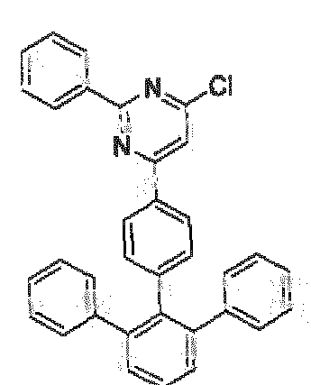


Claims


Priority Applications (4)
| Application Number | Priority Date | Filing Date | Title |
|---|---|---|---|
| CN202080070326.5A CN114555580A (en) | 2019-10-08 | 2020-10-08 | Compound, and organic semiconductor layer, organic electronic device, display device, and lighting device each comprising same |
| JP2022521153A JP2022551459A (en) | 2019-10-08 | 2020-10-08 | Compounds and organic semiconductor layers, organic electronic devices, display devices and lighting devices containing the same |
| KR1020227015212A KR20220079914A (en) | 2019-10-08 | 2020-10-08 | Compound and organic semiconducting layer comprising same, organic electronic device, display device and lighting device |
| EP20789574.9A EP4041716A1 (en) | 2019-10-08 | 2020-10-08 | Compound and an organic semiconducting layer, an organic electronic device, a display device and a lighting device comprising the same |
Applications Claiming Priority (2)
| Application Number | Priority Date | Filing Date | Title |
|---|---|---|---|
| EP19201931.3 | 2019-10-08 | ||
| EP19201931.3A EP3805206A1 (en) | 2019-10-08 | 2019-10-08 | Compound and an organic semiconducting layer, an organic electronic device, a display device and a lighting device comprising the same |
Publications (1)
| Publication Number | Publication Date |
|---|---|
| WO2021069595A1 true WO2021069595A1 (en) | 2021-04-15 |
Family
ID=68280681
Family Applications (1)
| Application Number | Title | Priority Date | Filing Date |
|---|---|---|---|
| PCT/EP2020/078287 WO2021069595A1 (en) | 2019-10-08 | 2020-10-08 | Compound and an organic semiconducting layer, an organic electronic device, a display device and a lighting device comprising the same |
Country Status (5)
| Country | Link |
|---|---|
| EP (2) | EP3805206A1 (en) |
| JP (1) | JP2022551459A (en) |
| KR (1) | KR20220079914A (en) |
| CN (1) | CN114555580A (en) |
| WO (1) | WO2021069595A1 (en) |
Families Citing this family (3)
| Publication number | Priority date | Publication date | Assignee | Title |
|---|---|---|---|---|
| EP4199125A1 (en) | 2021-12-14 | 2023-06-21 | Novaled GmbH | Organic light emitting diode, method for preparing the same and device comprising the same |
| EP4198103A1 (en) | 2021-12-14 | 2023-06-21 | Novaled GmbH | Organic light emitting diode and device comprising the same |
| EP4199133A1 (en) * | 2021-12-20 | 2023-06-21 | Novaled GmbH | Organic light emitting diode, display device comprising the same, and compound |
Citations (8)
| Publication number | Priority date | Publication date | Assignee | Title |
|---|---|---|---|---|
| EP1970371A1 (en) | 2007-03-16 | 2008-09-17 | Novaled AG | Pyrido(3,2-h)chinazolins and/or 5,6-Dihydro derivatives thereof, method for their manufacture and endowed organic semiconductor material containing them |
| WO2013079217A1 (en) | 2011-11-30 | 2013-06-06 | Novaled Ag | Display |
| EP2722908A1 (en) | 2012-10-17 | 2014-04-23 | Novaled AG | Phosphorescent OLED and hole transporting materials for phosphorescent OLEDs |
| KR20170093023A (en) | 2016-02-04 | 2017-08-14 | 삼성에스디아이 주식회사 | Organic compound for optoelectric device and organic optoelectric device and display device |
| KR20180093354A (en) * | 2017-02-13 | 2018-08-22 | (주)피엔에이치테크 | An electroluminescent compound and an electroluminescent device comprising the same |
| CN108997239A (en) * | 2018-07-25 | 2018-12-14 | 上海道亦化工科技有限公司 | A kind of compound of cyano-containing and application thereof and organic electroluminescence device |
| EP3502106A1 (en) * | 2017-12-21 | 2019-06-26 | Novaled GmbH | Triazine compounds substituted with bulky groups |
| WO2020126972A1 (en) * | 2018-12-21 | 2020-06-25 | Novaled Gmbh | Compound and an organic semiconducting layer, an organic electronic device and a display device comprising the same |
Family Cites Families (4)
| Publication number | Priority date | Publication date | Assignee | Title |
|---|---|---|---|---|
| KR101888934B1 (en) | 2015-04-24 | 2018-08-16 | 삼성에스디아이 주식회사 | Organic compound for optoelectric device andorganic optoelectric device and display device |
| EP3171418A1 (en) * | 2015-11-23 | 2017-05-24 | Novaled GmbH | Organic semiconductive layer comprising phosphine oxide compounds |
| CN109535093A (en) | 2018-12-24 | 2019-03-29 | 上海道亦化工科技有限公司 | A kind of trisubstituted benzene based compound and organic electroluminescence device |
| EP3766875A1 (en) * | 2019-07-15 | 2021-01-20 | Novaled GmbH | Compound and an organic semiconducting layer, an organic electronic device, a display device and a lighting device comprising the same |
-
2019
- 2019-10-08 EP EP19201931.3A patent/EP3805206A1/en active Pending
-
2020
- 2020-10-08 WO PCT/EP2020/078287 patent/WO2021069595A1/en unknown
- 2020-10-08 CN CN202080070326.5A patent/CN114555580A/en active Pending
- 2020-10-08 EP EP20789574.9A patent/EP4041716A1/en active Pending
- 2020-10-08 JP JP2022521153A patent/JP2022551459A/en active Pending
- 2020-10-08 KR KR1020227015212A patent/KR20220079914A/en unknown
Patent Citations (8)
| Publication number | Priority date | Publication date | Assignee | Title |
|---|---|---|---|---|
| EP1970371A1 (en) | 2007-03-16 | 2008-09-17 | Novaled AG | Pyrido(3,2-h)chinazolins and/or 5,6-Dihydro derivatives thereof, method for their manufacture and endowed organic semiconductor material containing them |
| WO2013079217A1 (en) | 2011-11-30 | 2013-06-06 | Novaled Ag | Display |
| EP2722908A1 (en) | 2012-10-17 | 2014-04-23 | Novaled AG | Phosphorescent OLED and hole transporting materials for phosphorescent OLEDs |
| KR20170093023A (en) | 2016-02-04 | 2017-08-14 | 삼성에스디아이 주식회사 | Organic compound for optoelectric device and organic optoelectric device and display device |
| KR20180093354A (en) * | 2017-02-13 | 2018-08-22 | (주)피엔에이치테크 | An electroluminescent compound and an electroluminescent device comprising the same |
| EP3502106A1 (en) * | 2017-12-21 | 2019-06-26 | Novaled GmbH | Triazine compounds substituted with bulky groups |
| CN108997239A (en) * | 2018-07-25 | 2018-12-14 | 上海道亦化工科技有限公司 | A kind of compound of cyano-containing and application thereof and organic electroluminescence device |
| WO2020126972A1 (en) * | 2018-12-21 | 2020-06-25 | Novaled Gmbh | Compound and an organic semiconducting layer, an organic electronic device and a display device comprising the same |
Non-Patent Citations (1)
| Title |
|---|
| YASUHIKO SHIROTAHIROSHI KAGEYAMA, CHEM. REV., vol. 107, 2007, pages 953 - 1010 |
Also Published As
| Publication number | Publication date |
|---|---|
| EP4041716A1 (en) | 2022-08-17 |
| EP3805206A1 (en) | 2021-04-14 |
| JP2022551459A (en) | 2022-12-09 |
| KR20220079914A (en) | 2022-06-14 |
| CN114555580A (en) | 2022-05-27 |
Similar Documents
| Publication | Publication Date | Title |
|---|---|---|
| EP3895226B1 (en) | Organic light emitting device and a compound for use therein | |
| WO2021009206A1 (en) | Compound and an organic semiconducting layer, an organic electronic device, a display device and a lighting device comprising the same | |
| EP3670504A1 (en) | Compound and an organic semiconducting layer, an organic electronic device and a display device comprising the same | |
| WO2019166270A1 (en) | Organic electronic device, display and lighting devices comprising the same | |
| WO2021069595A1 (en) | Compound and an organic semiconducting layer, an organic electronic device, a display device and a lighting device comprising the same | |
| WO2019166269A1 (en) | Spiro benzoanthracene-fluorene derivatives and their use in organic electronic devices, displays and lighting devices | |
| EP3480192B1 (en) | Triazine compound and organic semiconducting layer comprising the same | |
| WO2019201621A1 (en) | Compound, method for preparing the same, organic semiconducting layer, organic electronic device, display device and lighting device comprising the same | |
| US20220149290A1 (en) | Compound and an Organic Semiconducting Layer, an Organic Electronic Device and a Display or Lighting Device Comprising the Same | |
| US11524952B2 (en) | Compound and organic semiconducting layer, organic electronic device, display device and lighting device comprising the same | |
| WO2020148396A1 (en) | Compound and organic electronic device comprising the same | |
| EP4156314A1 (en) | Organic electronic device and a compound | |
| US20220209135A1 (en) | See addendum | |
| US20220131087A1 (en) | Compound and an Organic Semiconducting Layer, an Organic Electronic Device and a Display or Lighting Device Comprising the Same | |
| WO2024002883A1 (en) | Compound, organic semiconducting material comprising the same, organic electronic device comprising the same and a method for preparing the organic electronic device | |
| WO2023110610A1 (en) | Organic light emitting diode, method for preparing the same and device comprising the same | |
| WO2023025843A1 (en) | Organic light emitting diode and a compound for use therein | |
| WO2023213712A1 (en) | Organic light emitting diode and device comprising the same |
Legal Events
| Date | Code | Title | Description |
|---|---|---|---|
| 121 | Ep: the epo has been informed by wipo that ep was designated in this application |
Ref document number: 20789574 Country of ref document: EP Kind code of ref document: A1 |
|
| ENP | Entry into the national phase |
Ref document number: 2022521153 Country of ref document: JP Kind code of ref document: A |
|
| NENP | Non-entry into the national phase |
Ref country code: DE |
|
| ENP | Entry into the national phase |
Ref document number: 20227015212 Country of ref document: KR Kind code of ref document: A |
|
| ENP | Entry into the national phase |
Ref document number: 2020789574 Country of ref document: EP Effective date: 20220509 |