WO2021059086A1 - Organic compound, optical device, light emitting device, light emitting apparatus, electronic device, and lighting device - Google Patents
Organic compound, optical device, light emitting device, light emitting apparatus, electronic device, and lighting device Download PDFInfo
- Publication number
- WO2021059086A1 WO2021059086A1 PCT/IB2020/058589 IB2020058589W WO2021059086A1 WO 2021059086 A1 WO2021059086 A1 WO 2021059086A1 IB 2020058589 W IB2020058589 W IB 2020058589W WO 2021059086 A1 WO2021059086 A1 WO 2021059086A1
- Authority
- WO
- WIPO (PCT)
- Prior art keywords
- carbon atoms
- light emitting
- group
- groups
- emitting device
- Prior art date
Links
- 150000002894 organic compounds Chemical class 0.000 title claims abstract description 91
- 230000003287 optical effect Effects 0.000 title claims description 20
- 239000001257 hydrogen Substances 0.000 claims abstract description 59
- 229910052739 hydrogen Inorganic materials 0.000 claims abstract description 59
- 125000001997 phenyl group Chemical group [H]C1=C([H])C([H])=C(*)C([H])=C1[H] 0.000 claims abstract description 55
- 125000004093 cyano group Chemical group *C#N 0.000 claims abstract description 53
- 229910052736 halogen Inorganic materials 0.000 claims abstract description 51
- 150000002367 halogens Chemical class 0.000 claims abstract description 51
- 125000000753 cycloalkyl group Chemical group 0.000 claims abstract description 50
- 125000002029 aromatic hydrocarbon group Chemical group 0.000 claims abstract description 31
- 125000003118 aryl group Chemical group 0.000 claims abstract description 25
- 125000004432 carbon atom Chemical group C* 0.000 claims description 219
- 239000000758 substrate Substances 0.000 claims description 99
- 125000000217 alkyl group Chemical group 0.000 claims description 56
- 125000003545 alkoxy group Chemical group 0.000 claims description 44
- 125000001188 haloalkyl group Chemical group 0.000 claims description 44
- 229910052799 carbon Inorganic materials 0.000 claims description 39
- OKTJSMMVPCPJKN-UHFFFAOYSA-N Carbon Chemical compound [C] OKTJSMMVPCPJKN-UHFFFAOYSA-N 0.000 claims description 21
- XEEYBQQBJWHFJM-UHFFFAOYSA-N Iron Chemical compound [Fe] XEEYBQQBJWHFJM-UHFFFAOYSA-N 0.000 claims description 21
- HEDRZPFGACZZDS-UHFFFAOYSA-N Chloroform Chemical compound ClC(Cl)Cl HEDRZPFGACZZDS-UHFFFAOYSA-N 0.000 claims description 15
- UFHFLCQGNIYNRP-UHFFFAOYSA-N Hydrogen Chemical compound [H][H] UFHFLCQGNIYNRP-UHFFFAOYSA-N 0.000 claims description 14
- 125000004430 oxygen atom Chemical group O* 0.000 claims description 14
- 229910052717 sulfur Chemical group 0.000 claims description 13
- 125000004434 sulfur atom Chemical group 0.000 claims description 13
- 150000004945 aromatic hydrocarbons Chemical class 0.000 claims description 9
- 150000001721 carbon Chemical class 0.000 claims description 2
- 125000002496 methyl group Chemical group [H]C([H])([H])* 0.000 claims description 2
- 125000004435 hydrogen atom Chemical group [H]* 0.000 claims 14
- 125000001183 hydrocarbyl group Chemical group 0.000 claims 1
- 150000002431 hydrogen Chemical class 0.000 abstract description 32
- 125000004191 (C1-C6) alkoxy group Chemical group 0.000 abstract 2
- 125000004169 (C1-C6) alkyl group Chemical group 0.000 abstract 2
- 125000000171 (C1-C6) haloalkyl group Chemical group 0.000 abstract 2
- 239000010410 layer Substances 0.000 description 315
- YXFVVABEGXRONW-UHFFFAOYSA-N Toluene Chemical compound CC1=CC=CC=C1 YXFVVABEGXRONW-UHFFFAOYSA-N 0.000 description 174
- 239000000463 material Substances 0.000 description 170
- 238000005259 measurement Methods 0.000 description 112
- -1 arylamine compound Chemical class 0.000 description 93
- 239000010408 film Substances 0.000 description 92
- 239000000126 substance Substances 0.000 description 92
- 239000007787 solid Substances 0.000 description 91
- 229910052757 nitrogen Inorganic materials 0.000 description 83
- 238000000034 method Methods 0.000 description 72
- 230000015572 biosynthetic process Effects 0.000 description 67
- 238000003786 synthesis reaction Methods 0.000 description 65
- 238000000295 emission spectrum Methods 0.000 description 63
- 150000001875 compounds Chemical class 0.000 description 62
- 230000000052 comparative effect Effects 0.000 description 57
- 238000000862 absorption spectrum Methods 0.000 description 56
- 238000002347 injection Methods 0.000 description 56
- 239000007924 injection Substances 0.000 description 56
- 238000005401 electroluminescence Methods 0.000 description 54
- 239000000203 mixture Substances 0.000 description 48
- IJGRMHOSHXDMSA-UHFFFAOYSA-N Atomic nitrogen Chemical compound N#N IJGRMHOSHXDMSA-UHFFFAOYSA-N 0.000 description 47
- 239000000243 solution Substances 0.000 description 43
- 238000010438 heat treatment Methods 0.000 description 42
- 239000010409 thin film Substances 0.000 description 39
- 230000005284 excitation Effects 0.000 description 37
- 230000005525 hole transport Effects 0.000 description 33
- VLKZOEOYAKHREP-UHFFFAOYSA-N n-Hexane Chemical compound CCCCCC VLKZOEOYAKHREP-UHFFFAOYSA-N 0.000 description 33
- 238000004519 manufacturing process Methods 0.000 description 30
- 238000007740 vapor deposition Methods 0.000 description 30
- XLYOFNOQVPJJNP-UHFFFAOYSA-N water Substances O XLYOFNOQVPJJNP-UHFFFAOYSA-N 0.000 description 30
- 238000004770 highest occupied molecular orbital Methods 0.000 description 29
- 238000007789 sealing Methods 0.000 description 29
- 238000000859 sublimation Methods 0.000 description 29
- 230000008022 sublimation Effects 0.000 description 29
- ODHXBMXNKOYIBV-UHFFFAOYSA-N triphenylamine Chemical compound C1=CC=CC=C1N(C=1C=CC=CC=1)C1=CC=CC=C1 ODHXBMXNKOYIBV-UHFFFAOYSA-N 0.000 description 28
- CSNNHWWHGAXBCP-UHFFFAOYSA-L Magnesium sulfate Chemical compound [Mg+2].[O-][S+2]([O-])([O-])[O-] CSNNHWWHGAXBCP-UHFFFAOYSA-L 0.000 description 27
- MILUBEOXRNEUHS-UHFFFAOYSA-N iridium(3+) Chemical compound [Ir+3] MILUBEOXRNEUHS-UHFFFAOYSA-N 0.000 description 27
- 238000010521 absorption reaction Methods 0.000 description 26
- 239000004065 semiconductor Substances 0.000 description 26
- 230000006870 function Effects 0.000 description 25
- 238000004768 lowest unoccupied molecular orbital Methods 0.000 description 25
- 238000004455 differential thermal analysis Methods 0.000 description 24
- 239000003566 sealing material Substances 0.000 description 22
- 125000000319 biphenyl-4-yl group Chemical group [H]C1=C([H])C([H])=C([H])C([H])=C1C1=C([H])C([H])=C([*])C([H])=C1[H] 0.000 description 21
- QJGQUHMNIGDVPM-UHFFFAOYSA-N nitrogen group Chemical group [N] QJGQUHMNIGDVPM-UHFFFAOYSA-N 0.000 description 21
- MFRIHAYPQRLWNB-UHFFFAOYSA-N sodium tert-butoxide Chemical compound [Na+].CC(C)(C)[O-] MFRIHAYPQRLWNB-UHFFFAOYSA-N 0.000 description 21
- 0 CN(c(cc1)cc2c1C(C(*)=C(*)C(*)C1*)=C1C2(*)*)[Al] Chemical compound CN(c(cc1)cc2c1C(C(*)=C(*)C(*)C1*)=C1C2(*)*)[Al] 0.000 description 20
- 229910052751 metal Inorganic materials 0.000 description 20
- 239000002184 metal Substances 0.000 description 20
- 238000006243 chemical reaction Methods 0.000 description 19
- 239000002131 composite material Substances 0.000 description 19
- XKRFYHLGVUSROY-UHFFFAOYSA-N Argon Chemical compound [Ar] XKRFYHLGVUSROY-UHFFFAOYSA-N 0.000 description 18
- VYPSYNLAJGMNEJ-UHFFFAOYSA-N Silicium dioxide Chemical compound O=[Si]=O VYPSYNLAJGMNEJ-UHFFFAOYSA-N 0.000 description 18
- 239000011159 matrix material Substances 0.000 description 18
- 239000012044 organic layer Substances 0.000 description 18
- 230000009467 reduction Effects 0.000 description 18
- 238000007254 oxidation reaction Methods 0.000 description 17
- 238000005481 NMR spectroscopy Methods 0.000 description 16
- 239000007983 Tris buffer Substances 0.000 description 16
- 229910052782 aluminium Inorganic materials 0.000 description 16
- 238000000113 differential scanning calorimetry Methods 0.000 description 16
- 239000011521 glass Substances 0.000 description 16
- 125000001072 heteroaryl group Chemical group 0.000 description 16
- 230000003647 oxidation Effects 0.000 description 16
- 238000000746 purification Methods 0.000 description 16
- 238000005160 1H NMR spectroscopy Methods 0.000 description 15
- 238000010586 diagram Methods 0.000 description 14
- 239000000706 filtrate Substances 0.000 description 14
- BASFCYQUMIYNBI-UHFFFAOYSA-N platinum Chemical compound [Pt] BASFCYQUMIYNBI-UHFFFAOYSA-N 0.000 description 14
- KDLHZDBZIXYQEI-UHFFFAOYSA-N Palladium Chemical compound [Pd] KDLHZDBZIXYQEI-UHFFFAOYSA-N 0.000 description 13
- XLOMVQKBTHCTTD-UHFFFAOYSA-N Zinc monoxide Chemical compound [Zn]=O XLOMVQKBTHCTTD-UHFFFAOYSA-N 0.000 description 13
- CUJRVFIICFDLGR-UHFFFAOYSA-N acetylacetonate Chemical compound CC(=O)[CH-]C(C)=O CUJRVFIICFDLGR-UHFFFAOYSA-N 0.000 description 13
- 229910052783 alkali metal Inorganic materials 0.000 description 13
- 150000001340 alkali metals Chemical class 0.000 description 13
- XAGFODPZIPBFFR-UHFFFAOYSA-N aluminium Chemical compound [Al] XAGFODPZIPBFFR-UHFFFAOYSA-N 0.000 description 13
- UHOVQNZJYSORNB-UHFFFAOYSA-N Benzene Chemical compound C1=CC=CC=C1 UHOVQNZJYSORNB-UHFFFAOYSA-N 0.000 description 12
- CTQNGGLPUBDAKN-UHFFFAOYSA-N O-Xylene Chemical compound CC1=CC=CC=C1C CTQNGGLPUBDAKN-UHFFFAOYSA-N 0.000 description 12
- 238000002484 cyclic voltammetry Methods 0.000 description 12
- AMGQUBHHOARCQH-UHFFFAOYSA-N indium;oxotin Chemical compound [In].[Sn]=O AMGQUBHHOARCQH-UHFFFAOYSA-N 0.000 description 12
- 230000001681 protective effect Effects 0.000 description 12
- 238000010992 reflux Methods 0.000 description 12
- 230000001052 transient effect Effects 0.000 description 12
- 239000008096 xylene Substances 0.000 description 12
- UKSZBOKPHAQOMP-SVLSSHOZSA-N (1e,4e)-1,5-diphenylpenta-1,4-dien-3-one;palladium Chemical compound [Pd].C=1C=CC=CC=1\C=C\C(=O)\C=C\C1=CC=CC=C1.C=1C=CC=CC=1\C=C\C(=O)\C=C\C1=CC=CC=C1 UKSZBOKPHAQOMP-SVLSSHOZSA-N 0.000 description 11
- 230000008859 change Effects 0.000 description 11
- 238000004140 cleaning Methods 0.000 description 11
- 230000033116 oxidation-reduction process Effects 0.000 description 11
- HPALAKNZSZLMCH-UHFFFAOYSA-M sodium;chloride;hydrate Chemical class O.[Na+].[Cl-] HPALAKNZSZLMCH-UHFFFAOYSA-M 0.000 description 11
- 238000004544 sputter deposition Methods 0.000 description 11
- 125000001424 substituent group Chemical group 0.000 description 11
- 125000001637 1-naphthyl group Chemical group [H]C1=C([H])C([H])=C2C(*)=C([H])C([H])=C([H])C2=C1[H] 0.000 description 10
- 238000004364 calculation method Methods 0.000 description 10
- 229910052741 iridium Inorganic materials 0.000 description 10
- GKOZUEZYRPOHIO-UHFFFAOYSA-N iridium atom Chemical compound [Ir] GKOZUEZYRPOHIO-UHFFFAOYSA-N 0.000 description 10
- 239000000047 product Substances 0.000 description 10
- 229910052814 silicon oxide Inorganic materials 0.000 description 10
- 230000002194 synthesizing effect Effects 0.000 description 10
- 229910052786 argon Inorganic materials 0.000 description 9
- 125000000609 carbazolyl group Chemical group C1(=CC=CC=2C3=CC=CC=C3NC12)* 0.000 description 9
- 230000002950 deficient Effects 0.000 description 9
- 239000011229 interlayer Substances 0.000 description 9
- 239000002904 solvent Substances 0.000 description 9
- 238000003756 stirring Methods 0.000 description 9
- VIJYEGDOKCKUOL-UHFFFAOYSA-N 9-phenylcarbazole Chemical compound C1=CC=CC=C1N1C2=CC=CC=C2C2=CC=CC=C21 VIJYEGDOKCKUOL-UHFFFAOYSA-N 0.000 description 8
- YMTOLUWGNWPBLD-UHFFFAOYSA-N Nc1cc2ccccc2c2c1oc1ccccc21 Chemical compound Nc1cc2ccccc2c2c1oc1ccccc21 YMTOLUWGNWPBLD-UHFFFAOYSA-N 0.000 description 8
- MWPLVEDNUUSJAV-UHFFFAOYSA-N anthracene Chemical compound C1=CC=CC2=CC3=CC=CC=C3C=C21 MWPLVEDNUUSJAV-UHFFFAOYSA-N 0.000 description 8
- 239000002585 base Substances 0.000 description 8
- 230000008878 coupling Effects 0.000 description 8
- 238000010168 coupling process Methods 0.000 description 8
- 238000005859 coupling reaction Methods 0.000 description 8
- 238000000354 decomposition reaction Methods 0.000 description 8
- 230000009477 glass transition Effects 0.000 description 8
- 150000002391 heterocyclic compounds Chemical class 0.000 description 8
- 229910052943 magnesium sulfate Inorganic materials 0.000 description 8
- 235000019341 magnesium sulphate Nutrition 0.000 description 8
- 238000011084 recovery Methods 0.000 description 8
- 229910052710 silicon Inorganic materials 0.000 description 8
- 239000010703 silicon Substances 0.000 description 8
- 238000005092 sublimation method Methods 0.000 description 8
- 238000002411 thermogravimetry Methods 0.000 description 8
- 125000000391 vinyl group Chemical group [H]C([*])=C([H])[H] 0.000 description 8
- JUJWROOIHBZHMG-UHFFFAOYSA-N Pyridine Chemical class C1=CC=NC=C1 JUJWROOIHBZHMG-UHFFFAOYSA-N 0.000 description 7
- 229910052784 alkaline earth metal Inorganic materials 0.000 description 7
- 125000005577 anthracene group Chemical group 0.000 description 7
- 238000000231 atomic layer deposition Methods 0.000 description 7
- 125000005605 benzo group Chemical group 0.000 description 7
- YPZSGSCKNSSHJN-UHFFFAOYSA-N benzo[e][1]benzofuran-8-amine Chemical compound C1=COC2=C1C1=CC(=CC=C1C=C2)N YPZSGSCKNSSHJN-UHFFFAOYSA-N 0.000 description 7
- 239000000872 buffer Substances 0.000 description 7
- 239000003086 colorant Substances 0.000 description 7
- 238000000151 deposition Methods 0.000 description 7
- QMLPJDVGNRHGJQ-UHFFFAOYSA-N ditert-butyl-(1-methyl-2,2-diphenylcyclopropyl)phosphane Chemical compound CC(C)(C)P(C(C)(C)C)C1(C)CC1(C=1C=CC=CC=1)C1=CC=CC=C1 QMLPJDVGNRHGJQ-UHFFFAOYSA-N 0.000 description 7
- 230000000694 effects Effects 0.000 description 7
- 229910003437 indium oxide Inorganic materials 0.000 description 7
- PJXISJQVUVHSOJ-UHFFFAOYSA-N indium(iii) oxide Chemical compound [O-2].[O-2].[O-2].[In+3].[In+3] PJXISJQVUVHSOJ-UHFFFAOYSA-N 0.000 description 7
- 238000000691 measurement method Methods 0.000 description 7
- 238000005192 partition Methods 0.000 description 7
- 238000005424 photoluminescence Methods 0.000 description 7
- YLQBMQCUIZJEEH-UHFFFAOYSA-N tetrahydrofuran Natural products C=1C=COC=1 YLQBMQCUIZJEEH-UHFFFAOYSA-N 0.000 description 7
- BWHDROKFUHTORW-UHFFFAOYSA-N tritert-butylphosphane Chemical compound CC(C)(C)P(C(C)(C)C)C(C)(C)C BWHDROKFUHTORW-UHFFFAOYSA-N 0.000 description 7
- 239000011701 zinc Substances 0.000 description 7
- XESMNQMWRSEIET-UHFFFAOYSA-N 2,9-dinaphthalen-2-yl-4,7-diphenyl-1,10-phenanthroline Chemical compound C1=CC=CC=C1C1=CC(C=2C=C3C=CC=CC3=CC=2)=NC2=C1C=CC1=C(C=3C=CC=CC=3)C=C(C=3C=C4C=CC=CC4=CC=3)N=C21 XESMNQMWRSEIET-UHFFFAOYSA-N 0.000 description 6
- VFUDMQLBKNMONU-UHFFFAOYSA-N 9-[4-(4-carbazol-9-ylphenyl)phenyl]carbazole Chemical group C12=CC=CC=C2C2=CC=CC=C2N1C1=CC=C(C=2C=CC(=CC=2)N2C3=CC=CC=C3C3=CC=CC=C32)C=C1 VFUDMQLBKNMONU-UHFFFAOYSA-N 0.000 description 6
- UJOBWOGCFQCDNV-UHFFFAOYSA-N 9H-carbazole Chemical compound C1=CC=C2C3=CC=CC=C3NC2=C1 UJOBWOGCFQCDNV-UHFFFAOYSA-N 0.000 description 6
- WKBOTKDWSSQWDR-UHFFFAOYSA-N Bromine atom Chemical compound [Br] WKBOTKDWSSQWDR-UHFFFAOYSA-N 0.000 description 6
- ZAMOUSCENKQFHK-UHFFFAOYSA-N Chlorine atom Chemical compound [Cl] ZAMOUSCENKQFHK-UHFFFAOYSA-N 0.000 description 6
- CBENFWSGALASAD-UHFFFAOYSA-N Ozone Chemical compound [O-][O+]=O CBENFWSGALASAD-UHFFFAOYSA-N 0.000 description 6
- NRTOMJZYCJJWKI-UHFFFAOYSA-N Titanium nitride Chemical compound [Ti]#N NRTOMJZYCJJWKI-UHFFFAOYSA-N 0.000 description 6
- 125000005595 acetylacetonate group Chemical group 0.000 description 6
- 150000001342 alkaline earth metals Chemical class 0.000 description 6
- 229910045601 alloy Inorganic materials 0.000 description 6
- 239000000956 alloy Substances 0.000 description 6
- 150000004982 aromatic amines Chemical group 0.000 description 6
- 239000012298 atmosphere Substances 0.000 description 6
- GDTBXPJZTBHREO-UHFFFAOYSA-N bromine Substances BrBr GDTBXPJZTBHREO-UHFFFAOYSA-N 0.000 description 6
- 229910052794 bromium Inorganic materials 0.000 description 6
- 150000004649 carbonic acid derivatives Chemical class 0.000 description 6
- 239000000460 chlorine Substances 0.000 description 6
- 229910052801 chlorine Inorganic materials 0.000 description 6
- 239000010949 copper Substances 0.000 description 6
- TXCDCPKCNAJMEE-UHFFFAOYSA-N dibenzofuran Chemical group C1=CC=C2C3=CC=CC=C3OC2=C1 TXCDCPKCNAJMEE-UHFFFAOYSA-N 0.000 description 6
- YMWUJEATGCHHMB-DICFDUPASA-N dichloromethane-d2 Chemical compound [2H]C([2H])(Cl)Cl YMWUJEATGCHHMB-DICFDUPASA-N 0.000 description 6
- 239000000284 extract Substances 0.000 description 6
- 150000004820 halides Chemical class 0.000 description 6
- 239000012299 nitrogen atmosphere Substances 0.000 description 6
- 239000012074 organic phase Substances 0.000 description 6
- 125000003373 pyrazinyl group Chemical group 0.000 description 6
- 239000010453 quartz Substances 0.000 description 6
- 238000010898 silica gel chromatography Methods 0.000 description 6
- VNFWTIYUKDMAOP-UHFFFAOYSA-N sphos Chemical group COC1=CC=CC(OC)=C1C1=CC=CC=C1P(C1CCCCC1)C1CCCCC1 VNFWTIYUKDMAOP-UHFFFAOYSA-N 0.000 description 6
- 238000012546 transfer Methods 0.000 description 6
- LENZDBCJOHFCAS-UHFFFAOYSA-N tris Chemical compound OCC(N)(CO)CO LENZDBCJOHFCAS-UHFFFAOYSA-N 0.000 description 6
- 239000011787 zinc oxide Substances 0.000 description 6
- HZFNDVDPBSUUAH-UHFFFAOYSA-N C1=CC=C(C=C1)C2=CC=CC=C2NC3=CC4=CC=CC=C4C5=C3OC6=CC=CC=C65 Chemical compound C1=CC=C(C=C1)C2=CC=CC=C2NC3=CC4=CC=CC=C4C5=C3OC6=CC=CC=C65 HZFNDVDPBSUUAH-UHFFFAOYSA-N 0.000 description 5
- RYGMFSIKBFXOCR-UHFFFAOYSA-N Copper Chemical compound [Cu] RYGMFSIKBFXOCR-UHFFFAOYSA-N 0.000 description 5
- 229910008449 SnF 2 Inorganic materials 0.000 description 5
- 238000004458 analytical method Methods 0.000 description 5
- 229910052802 copper Inorganic materials 0.000 description 5
- ZUOUZKKEUPVFJK-UHFFFAOYSA-N diphenyl Chemical group C1=CC=CC=C1C1=CC=CC=C1 ZUOUZKKEUPVFJK-UHFFFAOYSA-N 0.000 description 5
- 125000006575 electron-withdrawing group Chemical group 0.000 description 5
- 239000012212 insulator Substances 0.000 description 5
- 229910052744 lithium Inorganic materials 0.000 description 5
- 239000011777 magnesium Substances 0.000 description 5
- CUDNXVFCWNHCGM-UHFFFAOYSA-N naphtho[2,1-b][1]benzofuran-8-amine Chemical compound C1=CC=CC=2C=CC3=C(C=4C(O3)=C(C=CC=4)N)C1=2 CUDNXVFCWNHCGM-UHFFFAOYSA-N 0.000 description 5
- NIHNNTQXNPWCJQ-UHFFFAOYSA-N o-biphenylenemethane Natural products C1=CC=C2CC3=CC=CC=C3C2=C1 NIHNNTQXNPWCJQ-UHFFFAOYSA-N 0.000 description 5
- 229910052763 palladium Inorganic materials 0.000 description 5
- 229910052697 platinum Inorganic materials 0.000 description 5
- 229920000642 polymer Polymers 0.000 description 5
- 125000000714 pyrimidinyl group Chemical group 0.000 description 5
- 229910052761 rare earth metal Inorganic materials 0.000 description 5
- 150000002910 rare earth metals Chemical class 0.000 description 5
- 238000005215 recombination Methods 0.000 description 5
- 230000006798 recombination Effects 0.000 description 5
- 238000006467 substitution reaction Methods 0.000 description 5
- SPDPTFAJSFKAMT-UHFFFAOYSA-N 1-n-[4-[4-(n-[4-(3-methyl-n-(3-methylphenyl)anilino)phenyl]anilino)phenyl]phenyl]-4-n,4-n-bis(3-methylphenyl)-1-n-phenylbenzene-1,4-diamine Chemical compound CC1=CC=CC(N(C=2C=CC(=CC=2)N(C=2C=CC=CC=2)C=2C=CC(=CC=2)C=2C=CC(=CC=2)N(C=2C=CC=CC=2)C=2C=CC(=CC=2)N(C=2C=C(C)C=CC=2)C=2C=C(C)C=CC=2)C=2C=C(C)C=CC=2)=C1 SPDPTFAJSFKAMT-UHFFFAOYSA-N 0.000 description 4
- 125000001622 2-naphthyl group Chemical group [H]C1=C([H])C([H])=C2C([H])=C(*)C([H])=C([H])C2=C1[H] 0.000 description 4
- MFWOWURWNZHYLA-UHFFFAOYSA-N 3-[3-(3-dibenzothiophen-4-ylphenyl)phenyl]phenanthro[9,10-b]pyrazine Chemical compound C1=CC=C2C3=NC(C=4C=CC=C(C=4)C=4C=CC=C(C=4)C4=C5SC=6C(C5=CC=C4)=CC=CC=6)=CN=C3C3=CC=CC=C3C2=C1 MFWOWURWNZHYLA-UHFFFAOYSA-N 0.000 description 4
- FCNCGHJSNVOIKE-UHFFFAOYSA-N 9,10-diphenylanthracene Chemical compound C1=CC=CC=C1C(C1=CC=CC=C11)=C(C=CC=C2)C2=C1C1=CC=CC=C1 FCNCGHJSNVOIKE-UHFFFAOYSA-N 0.000 description 4
- 229920000178 Acrylic resin Polymers 0.000 description 4
- 239000004925 Acrylic resin Substances 0.000 description 4
- 239000005749 Copper compound Substances 0.000 description 4
- 229920002430 Fibre-reinforced plastic Polymers 0.000 description 4
- ZMXDDKWLCZADIW-UHFFFAOYSA-N N,N-Dimethylformamide Chemical class CN(C)C=O ZMXDDKWLCZADIW-UHFFFAOYSA-N 0.000 description 4
- XYFCBTPGUUZFHI-UHFFFAOYSA-N Phosphine Chemical compound P XYFCBTPGUUZFHI-UHFFFAOYSA-N 0.000 description 4
- YTPLMLYBLZKORZ-UHFFFAOYSA-N Thiophene Chemical group C=1C=CSC=1 YTPLMLYBLZKORZ-UHFFFAOYSA-N 0.000 description 4
- 238000006887 Ullmann reaction Methods 0.000 description 4
- HCHKCACWOHOZIP-UHFFFAOYSA-N Zinc Chemical compound [Zn] HCHKCACWOHOZIP-UHFFFAOYSA-N 0.000 description 4
- YRKCREAYFQTBPV-UHFFFAOYSA-N acetylacetone Chemical compound CC(=O)CC(C)=O YRKCREAYFQTBPV-UHFFFAOYSA-N 0.000 description 4
- 150000001412 amines Chemical group 0.000 description 4
- FJDQFPXHSGXQBY-UHFFFAOYSA-L caesium carbonate Chemical compound [Cs+].[Cs+].[O-]C([O-])=O FJDQFPXHSGXQBY-UHFFFAOYSA-L 0.000 description 4
- 229910000024 caesium carbonate Inorganic materials 0.000 description 4
- XJHCXCQVJFPJIK-UHFFFAOYSA-M caesium fluoride Chemical compound [F-].[Cs+] XJHCXCQVJFPJIK-UHFFFAOYSA-M 0.000 description 4
- 239000011575 calcium Substances 0.000 description 4
- 239000003153 chemical reaction reagent Substances 0.000 description 4
- 150000001880 copper compounds Chemical class 0.000 description 4
- 239000013078 crystal Substances 0.000 description 4
- 238000007872 degassing Methods 0.000 description 4
- IYYZUPMFVPLQIF-UHFFFAOYSA-N dibenzothiophene Chemical compound C1=CC=C2C3=CC=CC=C3SC2=C1 IYYZUPMFVPLQIF-UHFFFAOYSA-N 0.000 description 4
- GUVUOGQBMYCBQP-UHFFFAOYSA-N dmpu Chemical compound CN1CCCN(C)C1=O GUVUOGQBMYCBQP-UHFFFAOYSA-N 0.000 description 4
- 239000000428 dust Substances 0.000 description 4
- 239000011151 fibre-reinforced plastic Substances 0.000 description 4
- 125000000623 heterocyclic group Chemical group 0.000 description 4
- 238000004128 high performance liquid chromatography Methods 0.000 description 4
- 150000002503 iridium Chemical class 0.000 description 4
- PQXKHYXIUOZZFA-UHFFFAOYSA-M lithium fluoride Chemical compound [Li+].[F-] PQXKHYXIUOZZFA-UHFFFAOYSA-M 0.000 description 4
- QGLKJKCYBOYXKC-UHFFFAOYSA-N nonaoxidotritungsten Chemical compound O=[W]1(=O)O[W](=O)(=O)O[W](=O)(=O)O1 QGLKJKCYBOYXKC-UHFFFAOYSA-N 0.000 description 4
- 229920002620 polyvinyl fluoride Polymers 0.000 description 4
- BWHMMNNQKKPAPP-UHFFFAOYSA-L potassium carbonate Chemical compound [K+].[K+].[O-]C([O-])=O BWHMMNNQKKPAPP-UHFFFAOYSA-L 0.000 description 4
- 239000011347 resin Substances 0.000 description 4
- 229920005989 resin Polymers 0.000 description 4
- 238000002834 transmittance Methods 0.000 description 4
- 229910001930 tungsten oxide Inorganic materials 0.000 description 4
- 238000005406 washing Methods 0.000 description 4
- 229910052725 zinc Inorganic materials 0.000 description 4
- HTPBWAPZAJWXKY-UHFFFAOYSA-L zinc;quinolin-8-olate Chemical compound [Zn+2].C1=CN=C2C([O-])=CC=CC2=C1.C1=CN=C2C([O-])=CC=CC2=C1 HTPBWAPZAJWXKY-UHFFFAOYSA-L 0.000 description 4
- JFHIIYSJKXQYIJ-UHFFFAOYSA-N 7-[4-(10-phenyl-9-anthryl)phenyl]-7h-dibenzo[c,g]carbazole Chemical compound C1=CC=CC=C1C(C1=CC=CC=C11)=C(C=CC=C2)C2=C1C1=CC=C(N2C3=C(C4=CC=CC=C4C=C3)C3=C4C=CC=CC4=CC=C32)C=C1 JFHIIYSJKXQYIJ-UHFFFAOYSA-N 0.000 description 3
- IFFZVKXEHGJBIA-UHFFFAOYSA-N 9-naphthalen-1-yl-10-(4-naphthalen-2-ylphenyl)anthracene Chemical compound C12=CC=CC=C2C(C2=CC=C(C=C2)C2=CC3=CC=CC=C3C=C2)=C(C=CC=C2)C2=C1C1=CC=CC2=CC=CC=C12 IFFZVKXEHGJBIA-UHFFFAOYSA-N 0.000 description 3
- CFRFHWQYWJMEJN-UHFFFAOYSA-N 9h-fluoren-2-amine Chemical group C1=CC=C2C3=CC=C(N)C=C3CC2=C1 CFRFHWQYWJMEJN-UHFFFAOYSA-N 0.000 description 3
- 238000006443 Buchwald-Hartwig cross coupling reaction Methods 0.000 description 3
- YMWUJEATGCHHMB-UHFFFAOYSA-N Dichloromethane Chemical compound ClCCl YMWUJEATGCHHMB-UHFFFAOYSA-N 0.000 description 3
- XEKOWRVHYACXOJ-UHFFFAOYSA-N Ethyl acetate Chemical compound CCOC(C)=O XEKOWRVHYACXOJ-UHFFFAOYSA-N 0.000 description 3
- KRHYYFGTRYWZRS-UHFFFAOYSA-M Fluoride anion Chemical compound [F-] KRHYYFGTRYWZRS-UHFFFAOYSA-M 0.000 description 3
- PXHVJJICTQNCMI-UHFFFAOYSA-N Nickel Chemical compound [Ni] PXHVJJICTQNCMI-UHFFFAOYSA-N 0.000 description 3
- YNPNZTXNASCQKK-UHFFFAOYSA-N Phenanthrene Natural products C1=CC=C2C3=CC=CC=C3C=CC2=C1 YNPNZTXNASCQKK-UHFFFAOYSA-N 0.000 description 3
- 229910052581 Si3N4 Inorganic materials 0.000 description 3
- XUIMIQQOPSSXEZ-UHFFFAOYSA-N Silicon Chemical compound [Si] XUIMIQQOPSSXEZ-UHFFFAOYSA-N 0.000 description 3
- DGEZNRSVGBDHLK-UHFFFAOYSA-N [1,10]phenanthroline Chemical compound C1=CN=C2C3=NC=CC=C3C=CC2=C1 DGEZNRSVGBDHLK-UHFFFAOYSA-N 0.000 description 3
- 230000001133 acceleration Effects 0.000 description 3
- MFMVRILBADIIJO-UHFFFAOYSA-N benzo[e][1]benzofuran Chemical compound C1=CC=C2C(C=CO3)=C3C=CC2=C1 MFMVRILBADIIJO-UHFFFAOYSA-N 0.000 description 3
- JFDZBHWFFUWGJE-UHFFFAOYSA-N benzonitrile Chemical compound N#CC1=CC=CC=C1 JFDZBHWFFUWGJE-UHFFFAOYSA-N 0.000 description 3
- 229910052791 calcium Inorganic materials 0.000 description 3
- 239000000969 carrier Substances 0.000 description 3
- 239000003054 catalyst Substances 0.000 description 3
- 239000007795 chemical reaction product Substances 0.000 description 3
- 238000005229 chemical vapour deposition Methods 0.000 description 3
- 239000011651 chromium Substances 0.000 description 3
- 238000004891 communication Methods 0.000 description 3
- 229940125904 compound 1 Drugs 0.000 description 3
- 229940126214 compound 3 Drugs 0.000 description 3
- 229940125898 compound 5 Drugs 0.000 description 3
- 230000007547 defect Effects 0.000 description 3
- 230000003111 delayed effect Effects 0.000 description 3
- 239000000412 dendrimer Substances 0.000 description 3
- 229920000736 dendritic polymer Polymers 0.000 description 3
- 125000005331 diazinyl group Chemical group N1=NC(=CC=C1)* 0.000 description 3
- IYYZUPMFVPLQIF-ALWQSETLSA-N dibenzothiophene Chemical group C1=CC=CC=2[34S]C3=C(C=21)C=CC=C3 IYYZUPMFVPLQIF-ALWQSETLSA-N 0.000 description 3
- DKHNGUNXLDCATP-UHFFFAOYSA-N dipyrazino[2,3-f:2',3'-h]quinoxaline-2,3,6,7,10,11-hexacarbonitrile Chemical group C12=NC(C#N)=C(C#N)N=C2C2=NC(C#N)=C(C#N)N=C2C2=C1N=C(C#N)C(C#N)=N2 DKHNGUNXLDCATP-UHFFFAOYSA-N 0.000 description 3
- 230000005684 electric field Effects 0.000 description 3
- 125000003983 fluorenyl group Chemical group C1(=CC=CC=2C3=CC=CC=C3CC12)* 0.000 description 3
- 229910052735 hafnium Inorganic materials 0.000 description 3
- 238000003384 imaging method Methods 0.000 description 3
- 125000002883 imidazolyl group Chemical group 0.000 description 3
- 229910052738 indium Inorganic materials 0.000 description 3
- APFVFJFRJDLVQX-UHFFFAOYSA-N indium atom Chemical compound [In] APFVFJFRJDLVQX-UHFFFAOYSA-N 0.000 description 3
- KMGCVGZFTMILPV-UHFFFAOYSA-N iridium(3+);pentane-2,4-dione Chemical compound [Ir+3].CC(=O)CC(C)=O KMGCVGZFTMILPV-UHFFFAOYSA-N 0.000 description 3
- 239000003446 ligand Substances 0.000 description 3
- 125000000040 m-tolyl group Chemical group [H]C1=C([H])C(*)=C([H])C(=C1[H])C([H])([H])[H] 0.000 description 3
- 229910052749 magnesium Inorganic materials 0.000 description 3
- 230000007246 mechanism Effects 0.000 description 3
- 239000012528 membrane Substances 0.000 description 3
- 229910044991 metal oxide Inorganic materials 0.000 description 3
- 150000004706 metal oxides Chemical class 0.000 description 3
- 238000002156 mixing Methods 0.000 description 3
- 125000001624 naphthyl group Chemical group 0.000 description 3
- 150000004767 nitrides Chemical class 0.000 description 3
- 125000002524 organometallic group Chemical group 0.000 description 3
- NFHFRUOZVGFOOS-UHFFFAOYSA-N palladium;triphenylphosphane Chemical compound [Pd].C1=CC=CC=C1P(C=1C=CC=CC=1)C1=CC=CC=C1.C1=CC=CC=C1P(C=1C=CC=CC=1)C1=CC=CC=C1.C1=CC=CC=C1P(C=1C=CC=CC=1)C1=CC=CC=C1.C1=CC=CC=C1P(C=1C=CC=CC=1)C1=CC=CC=C1 NFHFRUOZVGFOOS-UHFFFAOYSA-N 0.000 description 3
- 125000002080 perylenyl group Chemical group C1(=CC=C2C=CC=C3C4=CC=CC5=CC=CC(C1=C23)=C45)* 0.000 description 3
- IEQIEDJGQAUEQZ-UHFFFAOYSA-N phthalocyanine Chemical compound N1C(N=C2C3=CC=CC=C3C(N=C3C4=CC=CC=C4C(=N4)N3)=N2)=C(C=CC=C2)C2=C1N=C1C2=CC=CC=C2C4=N1 IEQIEDJGQAUEQZ-UHFFFAOYSA-N 0.000 description 3
- 125000006239 protecting group Chemical group 0.000 description 3
- 239000002994 raw material Substances 0.000 description 3
- 230000004044 response Effects 0.000 description 3
- HQVNEWCFYHHQES-UHFFFAOYSA-N silicon nitride Chemical compound N12[Si]34N5[Si]62N3[Si]51N64 HQVNEWCFYHHQES-UHFFFAOYSA-N 0.000 description 3
- 238000004528 spin coating Methods 0.000 description 3
- 238000003860 storage Methods 0.000 description 3
- 150000003568 thioethers Chemical class 0.000 description 3
- 229910052719 titanium Inorganic materials 0.000 description 3
- 239000010936 titanium Substances 0.000 description 3
- 238000009849 vacuum degassing Methods 0.000 description 3
- 238000001771 vacuum deposition Methods 0.000 description 3
- 239000003981 vehicle Substances 0.000 description 3
- JYEUMXHLPRZUAT-UHFFFAOYSA-N 1,2,3-triazine Chemical compound C1=CN=NN=C1 JYEUMXHLPRZUAT-UHFFFAOYSA-N 0.000 description 2
- RYHBNJHYFVUHQT-UHFFFAOYSA-N 1,4-Dioxane Chemical compound C1COCCO1 RYHBNJHYFVUHQT-UHFFFAOYSA-N 0.000 description 2
- UHXOHPVVEHBKKT-UHFFFAOYSA-N 1-(2,2-diphenylethenyl)-4-[4-(2,2-diphenylethenyl)phenyl]benzene Chemical group C=1C=C(C=2C=CC(C=C(C=3C=CC=CC=3)C=3C=CC=CC=3)=CC=2)C=CC=1C=C(C=1C=CC=CC=1)C1=CC=CC=C1 UHXOHPVVEHBKKT-UHFFFAOYSA-N 0.000 description 2
- PKJBWOWQJHHAHG-UHFFFAOYSA-N 1-bromo-4-phenylbenzene Chemical group C1=CC(Br)=CC=C1C1=CC=CC=C1 PKJBWOWQJHHAHG-UHFFFAOYSA-N 0.000 description 2
- XOYZGLGJSAZOAG-UHFFFAOYSA-N 1-n,1-n,4-n-triphenyl-4-n-[4-[4-(n-[4-(n-phenylanilino)phenyl]anilino)phenyl]phenyl]benzene-1,4-diamine Chemical group C1=CC=CC=C1N(C=1C=CC(=CC=1)N(C=1C=CC=CC=1)C=1C=CC(=CC=1)C=1C=CC(=CC=1)N(C=1C=CC=CC=1)C=1C=CC(=CC=1)N(C=1C=CC=CC=1)C=1C=CC=CC=1)C1=CC=CC=C1 XOYZGLGJSAZOAG-UHFFFAOYSA-N 0.000 description 2
- ZABORCXHTNWZRV-UHFFFAOYSA-N 10-[4-(4,6-diphenyl-1,3,5-triazin-2-yl)phenyl]phenoxazine Chemical compound O1C2=CC=CC=C2N(C2=CC=C(C=C2)C2=NC(=NC(=N2)C2=CC=CC=C2)C2=CC=CC=C2)C2=C1C=CC=C2 ZABORCXHTNWZRV-UHFFFAOYSA-N 0.000 description 2
- MYKQKWIPLZEVOW-UHFFFAOYSA-N 11h-benzo[a]carbazole Chemical group C1=CC2=CC=CC=C2C2=C1C1=CC=CC=C1N2 MYKQKWIPLZEVOW-UHFFFAOYSA-N 0.000 description 2
- BFTIPCRZWILUIY-UHFFFAOYSA-N 2,5,8,11-tetratert-butylperylene Chemical group CC(C)(C)C1=CC(C2=CC(C(C)(C)C)=CC=3C2=C2C=C(C=3)C(C)(C)C)=C3C2=CC(C(C)(C)C)=CC3=C1 BFTIPCRZWILUIY-UHFFFAOYSA-N 0.000 description 2
- CNSRBJWFPJMRFB-UHFFFAOYSA-N 2,8-diphenyl-4-[4-(9-phenylfluoren-9-yl)phenyl]dibenzothiophene Chemical compound C1=CC=CC=C1C1=CC=C(SC=2C3=CC(=CC=2C=2C=CC(=CC=2)C2(C4=CC=CC=C4C4=CC=CC=C42)C=2C=CC=CC=2)C=2C=CC=CC=2)C3=C1 CNSRBJWFPJMRFB-UHFFFAOYSA-N 0.000 description 2
- GEQBRULPNIVQPP-UHFFFAOYSA-N 2-[3,5-bis(1-phenylbenzimidazol-2-yl)phenyl]-1-phenylbenzimidazole Chemical compound C1=CC=CC=C1N1C2=CC=CC=C2N=C1C1=CC(C=2N(C3=CC=CC=C3N=2)C=2C=CC=CC=2)=CC(C=2N(C3=CC=CC=C3N=2)C=2C=CC=CC=2)=C1 GEQBRULPNIVQPP-UHFFFAOYSA-N 0.000 description 2
- VOZBMWWMIQGZGM-UHFFFAOYSA-N 2-[4-(9,10-dinaphthalen-2-ylanthracen-2-yl)phenyl]-1-phenylbenzimidazole Chemical compound C1=CC=CC=C1N1C2=CC=CC=C2N=C1C1=CC=C(C=2C=C3C(C=4C=C5C=CC=CC5=CC=4)=C4C=CC=CC4=C(C=4C=C5C=CC=CC5=CC=4)C3=CC=2)C=C1 VOZBMWWMIQGZGM-UHFFFAOYSA-N 0.000 description 2
- GWHSOUPRKHXZPK-UHFFFAOYSA-N 3,6-bis(3,5-diphenylphenyl)-9-phenylcarbazole Chemical compound C1=CC=CC=C1C1=CC(C=2C=CC=CC=2)=CC(C=2C=C3C4=CC(=CC=C4N(C=4C=CC=CC=4)C3=CC=2)C=2C=C(C=C(C=2)C=2C=CC=CC=2)C=2C=CC=CC=2)=C1 GWHSOUPRKHXZPK-UHFFFAOYSA-N 0.000 description 2
- ZVFQEOPUXVPSLB-UHFFFAOYSA-N 3-(4-tert-butylphenyl)-4-phenyl-5-(4-phenylphenyl)-1,2,4-triazole Chemical compound C1=CC(C(C)(C)C)=CC=C1C(N1C=2C=CC=CC=2)=NN=C1C1=CC=C(C=2C=CC=CC=2)C=C1 ZVFQEOPUXVPSLB-UHFFFAOYSA-N 0.000 description 2
- CINYXYWQPZSTOT-UHFFFAOYSA-N 3-[3-[3,5-bis(3-pyridin-3-ylphenyl)phenyl]phenyl]pyridine Chemical compound C1=CN=CC(C=2C=C(C=CC=2)C=2C=C(C=C(C=2)C=2C=C(C=CC=2)C=2C=NC=CC=2)C=2C=C(C=CC=2)C=2C=NC=CC=2)=C1 CINYXYWQPZSTOT-UHFFFAOYSA-N 0.000 description 2
- AZFHXIBNMPIGOD-UHFFFAOYSA-N 4-hydroxypent-3-en-2-one iridium Chemical compound [Ir].CC(O)=CC(C)=O.CC(O)=CC(C)=O.CC(O)=CC(C)=O AZFHXIBNMPIGOD-UHFFFAOYSA-N 0.000 description 2
- BGEVROQFKHXUQA-UHFFFAOYSA-N 71012-25-4 Chemical group C12=CC=CC=C2C2=CC=CC=C2C2=C1C1=CC=CC=C1N2 BGEVROQFKHXUQA-UHFFFAOYSA-N 0.000 description 2
- UCFDALUXSMNRHK-UHFFFAOYSA-N 9,9'-spirobi[fluorene]-2-amine Chemical compound C12=CC=CC=C2C2=CC=CC=C2C21C1=CC=CC=C1C1=CC=C(N)C=C12 UCFDALUXSMNRHK-UHFFFAOYSA-N 0.000 description 2
- QUSBGJQBCNEPES-UHFFFAOYSA-N 9,9-dimethyl-n-phenyl-n-[4-(9-phenylcarbazol-3-yl)phenyl]fluoren-2-amine Chemical compound C1=C2C(C)(C)C3=CC=CC=C3C2=CC=C1N(C=1C=CC(=CC=1)C=1C=C2C3=CC=CC=C3N(C=3C=CC=CC=3)C2=CC=1)C1=CC=CC=C1 QUSBGJQBCNEPES-UHFFFAOYSA-N 0.000 description 2
- CEUOADWQUHBFHM-UHFFFAOYSA-N 9,9-dimethylfluoren-4-amine Chemical compound C1=CC=C(N)C2=C1C(C)(C)C1=CC=CC=C12 CEUOADWQUHBFHM-UHFFFAOYSA-N 0.000 description 2
- 229910017073 AlLi Inorganic materials 0.000 description 2
- JOXINEHABREYAL-UHFFFAOYSA-N CC1(C2=C(C3=CC=CC=C31)C(=CC=C2)NC4=CC5=CC=CC=C5C6=C4OC7=CC=CC=C76)C Chemical compound CC1(C2=C(C3=CC=CC=C31)C(=CC=C2)NC4=CC5=CC=CC=C5C6=C4OC7=CC=CC=C76)C JOXINEHABREYAL-UHFFFAOYSA-N 0.000 description 2
- WOQFTLJYZJPGJT-UHFFFAOYSA-N CC1(C2=CC=CC=C2C3=C1C=C(C=C3)NC4=CC5=CC=CC=C5C6=C4OC7=CC=CC=C76)C Chemical compound CC1(C2=CC=CC=C2C3=C1C=C(C=C3)NC4=CC5=CC=CC=C5C6=C4OC7=CC=CC=C76)C WOQFTLJYZJPGJT-UHFFFAOYSA-N 0.000 description 2
- OYPRJOBELJOOCE-UHFFFAOYSA-N Calcium Chemical compound [Ca] OYPRJOBELJOOCE-UHFFFAOYSA-N 0.000 description 2
- 229910052684 Cerium Inorganic materials 0.000 description 2
- VYZAMTAEIAYCRO-UHFFFAOYSA-N Chromium Chemical compound [Cr] VYZAMTAEIAYCRO-UHFFFAOYSA-N 0.000 description 2
- LFQSCWFLJHTTHZ-UHFFFAOYSA-N Ethanol Chemical compound CCO LFQSCWFLJHTTHZ-UHFFFAOYSA-N 0.000 description 2
- 229910002601 GaN Inorganic materials 0.000 description 2
- JMASRVWKEDWRBT-UHFFFAOYSA-N Gallium nitride Chemical compound [Ga]#N JMASRVWKEDWRBT-UHFFFAOYSA-N 0.000 description 2
- WHXSMMKQMYFTQS-UHFFFAOYSA-N Lithium Chemical compound [Li] WHXSMMKQMYFTQS-UHFFFAOYSA-N 0.000 description 2
- FYYHWMGAXLPEAU-UHFFFAOYSA-N Magnesium Chemical compound [Mg] FYYHWMGAXLPEAU-UHFFFAOYSA-N 0.000 description 2
- UFWIBTONFRDIAS-UHFFFAOYSA-N Naphthalene Chemical compound C1=CC=CC2=CC=CC=C21 UFWIBTONFRDIAS-UHFFFAOYSA-N 0.000 description 2
- 229920001609 Poly(3,4-ethylenedioxythiophene) Polymers 0.000 description 2
- CZPWVGJYEJSRLH-UHFFFAOYSA-N Pyrimidine Chemical compound C1=CN=CN=C1 CZPWVGJYEJSRLH-UHFFFAOYSA-N 0.000 description 2
- CDBYLPFSWZWCQE-UHFFFAOYSA-L Sodium Carbonate Chemical compound [Na+].[Na+].[O-]C([O-])=O CDBYLPFSWZWCQE-UHFFFAOYSA-L 0.000 description 2
- 235000002597 Solanum melongena Nutrition 0.000 description 2
- WYURNTSHIVDZCO-UHFFFAOYSA-N Tetrahydrofuran Chemical compound C1CCOC1 WYURNTSHIVDZCO-UHFFFAOYSA-N 0.000 description 2
- ATJFFYVFTNAWJD-UHFFFAOYSA-N Tin Chemical group [Sn] ATJFFYVFTNAWJD-UHFFFAOYSA-N 0.000 description 2
- RTAQQCXQSZGOHL-UHFFFAOYSA-N Titanium Chemical compound [Ti] RTAQQCXQSZGOHL-UHFFFAOYSA-N 0.000 description 2
- HEDRZPFGACZZDS-MICDWDOJSA-N Trichloro(2H)methane Chemical compound [2H]C(Cl)(Cl)Cl HEDRZPFGACZZDS-MICDWDOJSA-N 0.000 description 2
- DTQVDTLACAAQTR-UHFFFAOYSA-N Trifluoroacetic acid Chemical compound OC(=O)C(F)(F)F DTQVDTLACAAQTR-UHFFFAOYSA-N 0.000 description 2
- XHCLAFWTIXFWPH-UHFFFAOYSA-N [O-2].[O-2].[O-2].[O-2].[O-2].[V+5].[V+5] Chemical compound [O-2].[O-2].[O-2].[O-2].[O-2].[V+5].[V+5] XHCLAFWTIXFWPH-UHFFFAOYSA-N 0.000 description 2
- 238000002835 absorbance Methods 0.000 description 2
- DZBUGLKDJFMEHC-UHFFFAOYSA-N acridine Chemical compound C1=CC=CC2=CC3=CC=CC=C3N=C21 DZBUGLKDJFMEHC-UHFFFAOYSA-N 0.000 description 2
- 150000001339 alkali metal compounds Chemical class 0.000 description 2
- PNEYBMLMFCGWSK-UHFFFAOYSA-N aluminium oxide Inorganic materials [O-2].[O-2].[O-2].[Al+3].[Al+3] PNEYBMLMFCGWSK-UHFFFAOYSA-N 0.000 description 2
- 125000003277 amino group Chemical group 0.000 description 2
- 238000005452 bending Methods 0.000 description 2
- 230000008901 benefit Effects 0.000 description 2
- 125000006267 biphenyl group Chemical group 0.000 description 2
- 150000001716 carbazoles Chemical class 0.000 description 2
- 229910052804 chromium Inorganic materials 0.000 description 2
- 238000000576 coating method Methods 0.000 description 2
- 229940125782 compound 2 Drugs 0.000 description 2
- 239000004020 conductor Substances 0.000 description 2
- VPUGDVKSAQVFFS-UHFFFAOYSA-N coronene Chemical compound C1=C(C2=C34)C=CC3=CC=C(C=C3)C4=C4C3=CC=C(C=C3)C4=C2C3=C1 VPUGDVKSAQVFFS-UHFFFAOYSA-N 0.000 description 2
- 239000002274 desiccant Substances 0.000 description 2
- 230000006866 deterioration Effects 0.000 description 2
- 125000002147 dimethylamino group Chemical group [H]C([H])([H])N(*)C([H])([H])[H] 0.000 description 2
- 238000005516 engineering process Methods 0.000 description 2
- VQCBHWLJZDBHOS-UHFFFAOYSA-N erbium(iii) oxide Chemical compound O=[Er]O[Er]=O VQCBHWLJZDBHOS-UHFFFAOYSA-N 0.000 description 2
- 230000005281 excited state Effects 0.000 description 2
- 230000001747 exhibiting effect Effects 0.000 description 2
- 125000001153 fluoro group Chemical group F* 0.000 description 2
- 229910052733 gallium Inorganic materials 0.000 description 2
- 229910052732 germanium Inorganic materials 0.000 description 2
- 239000010931 gold Substances 0.000 description 2
- 238000007646 gravure printing Methods 0.000 description 2
- 125000005843 halogen group Chemical group 0.000 description 2
- 150000002430 hydrocarbons Chemical group 0.000 description 2
- AMWRITDGCCNYAT-UHFFFAOYSA-L hydroxy(oxo)manganese;manganese Chemical compound [Mn].O[Mn]=O.O[Mn]=O AMWRITDGCCNYAT-UHFFFAOYSA-L 0.000 description 2
- 238000005286 illumination Methods 0.000 description 2
- 239000012535 impurity Substances 0.000 description 2
- 150000007529 inorganic bases Chemical class 0.000 description 2
- MRELNEQAGSRDBK-UHFFFAOYSA-N lanthanum(3+);oxygen(2-) Chemical compound [O-2].[O-2].[O-2].[La+3].[La+3] MRELNEQAGSRDBK-UHFFFAOYSA-N 0.000 description 2
- 239000004973 liquid crystal related substance Substances 0.000 description 2
- XGZVUEUWXADBQD-UHFFFAOYSA-L lithium carbonate Chemical compound [Li+].[Li+].[O-]C([O-])=O XGZVUEUWXADBQD-UHFFFAOYSA-L 0.000 description 2
- 229910052808 lithium carbonate Inorganic materials 0.000 description 2
- FUJCRWPEOMXPAD-UHFFFAOYSA-N lithium oxide Chemical compound [Li+].[Li+].[O-2] FUJCRWPEOMXPAD-UHFFFAOYSA-N 0.000 description 2
- 229910001947 lithium oxide Inorganic materials 0.000 description 2
- CUONGYYJJVDODC-UHFFFAOYSA-N malononitrile Chemical compound N#CCC#N CUONGYYJJVDODC-UHFFFAOYSA-N 0.000 description 2
- 239000007769 metal material Substances 0.000 description 2
- IBHBKWKFFTZAHE-UHFFFAOYSA-N n-[4-[4-(n-naphthalen-1-ylanilino)phenyl]phenyl]-n-phenylnaphthalen-1-amine Chemical group C1=CC=CC=C1N(C=1C2=CC=CC=C2C=CC=1)C1=CC=C(C=2C=CC(=CC=2)N(C=2C=CC=CC=2)C=2C3=CC=CC=C3C=CC=2)C=C1 IBHBKWKFFTZAHE-UHFFFAOYSA-N 0.000 description 2
- 125000003261 o-tolyl group Chemical group [H]C1=C([H])C(*)=C(C([H])=C1[H])C([H])([H])[H] 0.000 description 2
- AHLBNYSZXLDEJQ-FWEHEUNISA-N orlistat Chemical compound CCCCCCCCCCC[C@H](OC(=O)[C@H](CC(C)C)NC=O)C[C@@H]1OC(=O)[C@H]1CCCCCC AHLBNYSZXLDEJQ-FWEHEUNISA-N 0.000 description 2
- 239000001301 oxygen Substances 0.000 description 2
- 229910052760 oxygen Inorganic materials 0.000 description 2
- YJVFFLUZDVXJQI-UHFFFAOYSA-L palladium(ii) acetate Chemical compound [Pd+2].CC([O-])=O.CC([O-])=O YJVFFLUZDVXJQI-UHFFFAOYSA-L 0.000 description 2
- 230000002093 peripheral effect Effects 0.000 description 2
- 239000012466 permeate Substances 0.000 description 2
- CSHWQDPOILHKBI-UHFFFAOYSA-N peryrene Natural products C1=CC(C2=CC=CC=3C2=C2C=CC=3)=C3C2=CC=CC3=C1 CSHWQDPOILHKBI-UHFFFAOYSA-N 0.000 description 2
- 239000012071 phase Substances 0.000 description 2
- 125000001484 phenothiazinyl group Chemical group C1(=CC=CC=2SC3=CC=CC=C3NC12)* 0.000 description 2
- 125000001644 phenoxazinyl group Chemical group C1(=CC=CC=2OC3=CC=CC=C3NC12)* 0.000 description 2
- 229910000073 phosphorus hydride Inorganic materials 0.000 description 2
- 229920003023 plastic Polymers 0.000 description 2
- 239000004033 plastic Substances 0.000 description 2
- 229920003227 poly(N-vinyl carbazole) Polymers 0.000 description 2
- 229920000728 polyester Polymers 0.000 description 2
- 150000004032 porphyrins Chemical class 0.000 description 2
- 229910000027 potassium carbonate Inorganic materials 0.000 description 2
- PBMFSQRYOILNGV-UHFFFAOYSA-N pyridazine Chemical group C1=CC=NN=C1 PBMFSQRYOILNGV-UHFFFAOYSA-N 0.000 description 2
- 125000000168 pyrrolyl group Chemical group 0.000 description 2
- 150000002909 rare earth metal compounds Chemical class 0.000 description 2
- YYMBJDOZVAITBP-UHFFFAOYSA-N rubrene Chemical compound C1=CC=CC=C1C(C1=C(C=2C=CC=CC=2)C2=CC=CC=C2C(C=2C=CC=CC=2)=C11)=C(C=CC=C2)C2=C1C1=CC=CC=C1 YYMBJDOZVAITBP-UHFFFAOYSA-N 0.000 description 2
- 238000003980 solgel method Methods 0.000 description 2
- 238000001228 spectrum Methods 0.000 description 2
- 229910052712 strontium Inorganic materials 0.000 description 2
- CIOAGBVUUVVLOB-UHFFFAOYSA-N strontium atom Chemical compound [Sr] CIOAGBVUUVVLOB-UHFFFAOYSA-N 0.000 description 2
- 238000000967 suction filtration Methods 0.000 description 2
- 150000003457 sulfones Chemical class 0.000 description 2
- FKHIFSZMMVMEQY-UHFFFAOYSA-N talc Chemical compound [Mg+2].[O-][Si]([O-])=O FKHIFSZMMVMEQY-UHFFFAOYSA-N 0.000 description 2
- JBQYATWDVHIOAR-UHFFFAOYSA-N tellanylidenegermanium Chemical compound [Te]=[Ge] JBQYATWDVHIOAR-UHFFFAOYSA-N 0.000 description 2
- LFKDJXLFVYVEFG-UHFFFAOYSA-N tert-butyl carbamate Chemical compound CC(C)(C)OC(N)=O LFKDJXLFVYVEFG-UHFFFAOYSA-N 0.000 description 2
- KBLZDCFTQSIIOH-UHFFFAOYSA-M tetrabutylazanium;perchlorate Chemical compound [O-]Cl(=O)(=O)=O.CCCC[N+](CCCC)(CCCC)CCCC KBLZDCFTQSIIOH-UHFFFAOYSA-M 0.000 description 2
- 230000008719 thickening Effects 0.000 description 2
- 229910052718 tin Inorganic materials 0.000 description 2
- WFKWXMTUELFFGS-UHFFFAOYSA-N tungsten Chemical compound [W] WFKWXMTUELFFGS-UHFFFAOYSA-N 0.000 description 2
- 229910052721 tungsten Inorganic materials 0.000 description 2
- 239000010937 tungsten Substances 0.000 description 2
- 238000000870 ultraviolet spectroscopy Methods 0.000 description 2
- 229910001935 vanadium oxide Inorganic materials 0.000 description 2
- 210000003462 vein Anatomy 0.000 description 2
- CXNIUSPIQKWYAI-UHFFFAOYSA-N xantphos Chemical compound C=12OC3=C(P(C=4C=CC=CC=4)C=4C=CC=CC=4)C=CC=C3C(C)(C)C2=CC=CC=1P(C=1C=CC=CC=1)C1=CC=CC=C1 CXNIUSPIQKWYAI-UHFFFAOYSA-N 0.000 description 2
- 229910052727 yttrium Inorganic materials 0.000 description 2
- 229910052726 zirconium Inorganic materials 0.000 description 2
- HAKVNWBUOCSHTR-UHFFFAOYSA-N (9,9-dimethylxanthen-1-yl)-diphenylphosphane Chemical compound C=12C(C)(C)C3=CC=CC=C3OC2=CC=CC=1P(C=1C=CC=CC=1)C1=CC=CC=C1 HAKVNWBUOCSHTR-UHFFFAOYSA-N 0.000 description 1
- IWZZBBJTIUYDPZ-DVACKJPTSA-N (z)-4-hydroxypent-3-en-2-one;iridium;2-phenylpyridine Chemical compound [Ir].C\C(O)=C\C(C)=O.[C-]1=CC=CC=C1C1=CC=CC=N1.[C-]1=CC=CC=C1C1=CC=CC=N1 IWZZBBJTIUYDPZ-DVACKJPTSA-N 0.000 description 1
- XGCDBGRZEKYHNV-UHFFFAOYSA-N 1,1-bis(diphenylphosphino)methane Chemical compound C=1C=CC=CC=1P(C=1C=CC=CC=1)CP(C=1C=CC=CC=1)C1=CC=CC=C1 XGCDBGRZEKYHNV-UHFFFAOYSA-N 0.000 description 1
- WJWOFBKLBKILJV-UHFFFAOYSA-N 1,2,3,4-benzotetrathiine Chemical compound S1SSSC2=CC=CC=C21 WJWOFBKLBKILJV-UHFFFAOYSA-N 0.000 description 1
- UPWZWQGQRNPKTE-UHFFFAOYSA-N 1,2,3-trimethylidenecyclopropane Chemical class C=C1C(=C)C1=C UPWZWQGQRNPKTE-UHFFFAOYSA-N 0.000 description 1
- RTSZQXSYCGBHMO-UHFFFAOYSA-N 1,2,4-trichloro-3-prop-1-ynoxybenzene Chemical compound CC#COC1=C(Cl)C=CC(Cl)=C1Cl RTSZQXSYCGBHMO-UHFFFAOYSA-N 0.000 description 1
- XFDYBCQHRPMIGD-UHFFFAOYSA-N 1-N,6-N-bis(3-methylphenyl)-1-N,6-N-bis[3-(9-phenylfluoren-9-yl)phenyl]pyrene-1,6-diamine Chemical compound CC1=CC=CC(N(C=2C=C(C=CC=2)C2(C3=CC=CC=C3C3=CC=CC=C32)C=2C=CC=CC=2)C=2C3=CC=C4C=CC(=C5C=CC(C3=C54)=CC=2)N(C=2C=C(C)C=CC=2)C=2C=C(C=CC=2)C2(C3=CC=CC=C3C3=CC=CC=C32)C=2C=CC=CC=2)=C1 XFDYBCQHRPMIGD-UHFFFAOYSA-N 0.000 description 1
- IPNLBJDLLBQZDZ-UHFFFAOYSA-N 1-N,6-N-diphenyl-1-N,6-N-bis[4-(9-phenylfluoren-9-yl)phenyl]pyrene-1,6-diamine Chemical compound C1=CC=CC=C1N(C=1C2=CC=C3C=CC(=C4C=CC(C2=C43)=CC=1)N(C=1C=CC=CC=1)C=1C=CC(=CC=1)C1(C2=CC=CC=C2C2=CC=CC=C21)C=1C=CC=CC=1)C1=CC=C(C2(C3=CC=CC=C3C3=CC=CC=C32)C=2C=CC=CC=2)C=C1 IPNLBJDLLBQZDZ-UHFFFAOYSA-N 0.000 description 1
- RMSGQZDGSZOJMU-UHFFFAOYSA-N 1-butyl-2-phenylbenzene Chemical group CCCCC1=CC=CC=C1C1=CC=CC=C1 RMSGQZDGSZOJMU-UHFFFAOYSA-N 0.000 description 1
- FQNVFRPAQRVHKO-UHFFFAOYSA-N 1-n,4-n-bis(4-methylphenyl)-1-n,4-n-diphenylbenzene-1,4-diamine Chemical compound C1=CC(C)=CC=C1N(C=1C=CC(=CC=1)N(C=1C=CC=CC=1)C=1C=CC(C)=CC=1)C1=CC=CC=C1 FQNVFRPAQRVHKO-UHFFFAOYSA-N 0.000 description 1
- JTEUQFURLJKAMI-UHFFFAOYSA-N 1-phenylbenzo[a]anthracene Chemical compound C1(=CC=CC2=CC=C3C=C4C=CC=CC4=CC3=C12)C1=CC=CC=C1 JTEUQFURLJKAMI-UHFFFAOYSA-N 0.000 description 1
- CYPVTICNYNXTQP-UHFFFAOYSA-N 10-[4-[4-(9,9-dimethylacridin-10-yl)phenyl]sulfonylphenyl]-9,9-dimethylacridine Chemical compound C12=CC=CC=C2C(C)(C)C2=CC=CC=C2N1C1=CC=C(S(=O)(=O)C=2C=CC(=CC=2)N2C3=CC=CC=C3C(C)(C)C3=CC=CC=C32)C=C1 CYPVTICNYNXTQP-UHFFFAOYSA-N 0.000 description 1
- ASXSTQHYXCIZRV-UHFFFAOYSA-N 10-phenylspiro[acridine-9,10'-anthracene]-9'-one Chemical compound C12=CC=CC=C2C(=O)C2=CC=CC=C2C1(C1=CC=CC=C11)C2=CC=CC=C2N1C1=CC=CC=C1 ASXSTQHYXCIZRV-UHFFFAOYSA-N 0.000 description 1
- QWENRTYMTSOGBR-UHFFFAOYSA-N 1H-1,2,3-Triazole Chemical group C=1C=NNN=1 QWENRTYMTSOGBR-UHFFFAOYSA-N 0.000 description 1
- OOWLPGTVRWFLCX-UHFFFAOYSA-N 2,3,6,7-tetramethyl-9,10-dinaphthalen-1-ylanthracene Chemical compound C1=CC=C2C(C=3C4=CC(C)=C(C)C=C4C(C=4C5=CC=CC=C5C=CC=4)=C4C=C(C(=CC4=3)C)C)=CC=CC2=C1 OOWLPGTVRWFLCX-UHFFFAOYSA-N 0.000 description 1
- JEBPFDQAOYARIB-UHFFFAOYSA-N 2,3,6,7-tetramethyl-9,10-dinaphthalen-2-ylanthracene Chemical compound C1=CC=CC2=CC(C=3C4=CC(C)=C(C)C=C4C(C=4C=C5C=CC=CC5=CC=4)=C4C=C(C(=CC4=3)C)C)=CC=C21 JEBPFDQAOYARIB-UHFFFAOYSA-N 0.000 description 1
- HQYLCTWBSBBHPN-UHFFFAOYSA-N 2,3-bis[4-(10-phenylanthracen-9-yl)phenyl]-6-pyridin-2-ylpyridine Chemical compound C1=CC=CC=C1C(C1=CC=CC=C11)=C(C=CC=C2)C2=C1C1=CC=C(C=2C(=NC(=CC=2)C=2N=CC=CC=2)C=2C=CC(=CC=2)C=2C3=CC=CC=C3C(C=3C=CC=CC=3)=C3C=CC=CC3=2)C=C1 HQYLCTWBSBBHPN-UHFFFAOYSA-N 0.000 description 1
- UOCMXZLNHQBBOS-UHFFFAOYSA-N 2-(1,3-benzoxazol-2-yl)phenol zinc Chemical compound [Zn].Oc1ccccc1-c1nc2ccccc2o1.Oc1ccccc1-c1nc2ccccc2o1 UOCMXZLNHQBBOS-UHFFFAOYSA-N 0.000 description 1
- YDNOJUAQBFXZCR-UHFFFAOYSA-N 2-(2,3,4,5,6-pentafluorophenyl)acetonitrile Chemical compound FC1=C(F)C(F)=C(CC#N)C(F)=C1F YDNOJUAQBFXZCR-UHFFFAOYSA-N 0.000 description 1
- GJLCPQHEVZERAU-UHFFFAOYSA-N 2-(3-dibenzothiophen-4-ylphenyl)-1-phenylbenzimidazole Chemical compound C1=CC=CC=C1N1C2=CC=CC=C2N=C1C1=CC=CC(C=2C=3SC4=CC=CC=C4C=3C=CC=2)=C1 GJLCPQHEVZERAU-UHFFFAOYSA-N 0.000 description 1
- FQJQNLKWTRGIEB-UHFFFAOYSA-N 2-(4-tert-butylphenyl)-5-[3-[5-(4-tert-butylphenyl)-1,3,4-oxadiazol-2-yl]phenyl]-1,3,4-oxadiazole Chemical compound C1=CC(C(C)(C)C)=CC=C1C1=NN=C(C=2C=C(C=CC=2)C=2OC(=NN=2)C=2C=CC(=CC=2)C(C)(C)C)O1 FQJQNLKWTRGIEB-UHFFFAOYSA-N 0.000 description 1
- YLYPIBBGWLKELC-RMKNXTFCSA-N 2-[2-[(e)-2-[4-(dimethylamino)phenyl]ethenyl]-6-methylpyran-4-ylidene]propanedinitrile Chemical compound C1=CC(N(C)C)=CC=C1\C=C\C1=CC(=C(C#N)C#N)C=C(C)O1 YLYPIBBGWLKELC-RMKNXTFCSA-N 0.000 description 1
- IXHWGNYCZPISET-UHFFFAOYSA-N 2-[4-(dicyanomethylidene)-2,3,5,6-tetrafluorocyclohexa-2,5-dien-1-ylidene]propanedinitrile Chemical compound FC1=C(F)C(=C(C#N)C#N)C(F)=C(F)C1=C(C#N)C#N IXHWGNYCZPISET-UHFFFAOYSA-N 0.000 description 1
- MBHPOBSZPYEADG-UHFFFAOYSA-N 2-bromo-9,9-dimethylfluorene Chemical compound C1=C(Br)C=C2C(C)(C)C3=CC=CC=C3C2=C1 MBHPOBSZPYEADG-UHFFFAOYSA-N 0.000 description 1
- MAPWCBIPDFZEEV-UHFFFAOYSA-N 2-naphthalen-1-yl-N,N-diphenylaniline Chemical compound C1(=CC=CC2=CC=CC=C12)C1=C(C=CC=C1)N(C1=CC=CC=C1)C1=CC=CC=C1 MAPWCBIPDFZEEV-UHFFFAOYSA-N 0.000 description 1
- TWBPWBPGNQWFSJ-UHFFFAOYSA-N 2-phenylaniline Chemical compound NC1=CC=CC=C1C1=CC=CC=C1 TWBPWBPGNQWFSJ-UHFFFAOYSA-N 0.000 description 1
- VQGHOUODWALEFC-UHFFFAOYSA-N 2-phenylpyridine Chemical compound C1=CC=CC=C1C1=CC=CC=N1 VQGHOUODWALEFC-UHFFFAOYSA-N 0.000 description 1
- IBHNCJLKIQIKFU-UHFFFAOYSA-N 2-tert-butyl-9,10-bis(2-naphthalen-1-ylphenyl)anthracene Chemical compound C1=CC=C2C(C3=CC=CC=C3C3=C4C=CC=CC4=C(C=4C(=CC=CC=4)C=4C5=CC=CC=C5C=CC=4)C4=CC=C(C=C43)C(C)(C)C)=CC=CC2=C1 IBHNCJLKIQIKFU-UHFFFAOYSA-N 0.000 description 1
- MNHPNCZSKTUPMB-UHFFFAOYSA-N 2-tert-butyl-9,10-bis(4-phenylphenyl)anthracene Chemical compound C=12C=CC=CC2=C(C=2C=CC(=CC=2)C=2C=CC=CC=2)C2=CC(C(C)(C)C)=CC=C2C=1C(C=C1)=CC=C1C1=CC=CC=C1 MNHPNCZSKTUPMB-UHFFFAOYSA-N 0.000 description 1
- OBAJPWYDYFEBTF-UHFFFAOYSA-N 2-tert-butyl-9,10-dinaphthalen-2-ylanthracene Chemical compound C1=CC=CC2=CC(C3=C4C=CC=CC4=C(C=4C=C5C=CC=CC5=CC=4)C4=CC=C(C=C43)C(C)(C)C)=CC=C21 OBAJPWYDYFEBTF-UHFFFAOYSA-N 0.000 description 1
- WBPXZSIKOVBSAS-UHFFFAOYSA-N 2-tert-butylanthracene Chemical compound C1=CC=CC2=CC3=CC(C(C)(C)C)=CC=C3C=C21 WBPXZSIKOVBSAS-UHFFFAOYSA-N 0.000 description 1
- FTZXDZQJFKXEGW-UHFFFAOYSA-N 3-(9,9-dimethylacridin-10-yl)xanthen-9-one Chemical compound C12=CC=CC=C2C(C)(C)C2=CC=CC=C2N1C1=CC=C2C(=O)C3=CC=CC=C3OC2=C1 FTZXDZQJFKXEGW-UHFFFAOYSA-N 0.000 description 1
- GKTLHQFSIDFAJH-UHFFFAOYSA-N 3-(9h-carbazol-3-yl)-9-phenylcarbazole Chemical group C1=CC=CC=C1N1C2=CC=C(C=3C=C4C5=CC=CC=C5NC4=CC=3)C=C2C2=CC=CC=C21 GKTLHQFSIDFAJH-UHFFFAOYSA-N 0.000 description 1
- LLDZJTIZVZFNCM-UHFFFAOYSA-J 3-[18-(2-carboxyethyl)-8,13-diethyl-3,7,12,17-tetramethylporphyrin-21,24-diid-2-yl]propanoic acid;dichlorotin(2+) Chemical compound [H+].[H+].[Cl-].[Cl-].[Sn+4].[N-]1C(C=C2C(=C(C)C(=CC=3C(=C(C)C(=C4)N=3)CC)[N-]2)CCC([O-])=O)=C(CCC([O-])=O)C(C)=C1C=C1C(C)=C(CC)C4=N1 LLDZJTIZVZFNCM-UHFFFAOYSA-J 0.000 description 1
- PCUTZMWETFJZDZ-UHFFFAOYSA-N 3-[3-(3-carbazol-9-ylphenyl)phenyl]phenanthro[9,10-b]pyrazine Chemical compound C12=CC=CC=C2C2=CC=CC=C2N1C1=CC(C=2C=CC=C(C=2)C=2N=C3C4=CC=CC=C4C4=CC=CC=C4C3=NC=2)=CC=C1 PCUTZMWETFJZDZ-UHFFFAOYSA-N 0.000 description 1
- KYYFFLQBMZRHNB-UHFFFAOYSA-N 3-[9-(4,6-diphenyl-1,3,5-triazin-2-yl)carbazol-3-yl]-9-phenylcarbazole Chemical compound C1=CC=CC=C1C1=NC(C=2C=CC=CC=2)=NC(N2C3=CC=C(C=C3C3=CC=CC=C32)C=2C=C3C4=CC=CC=C4N(C=4C=CC=CC=4)C3=CC=2)=N1 KYYFFLQBMZRHNB-UHFFFAOYSA-N 0.000 description 1
- QVSJCRDHNCCXFC-UHFFFAOYSA-N 3-[9-[4-(4,6-diphenyl-1,3,5-triazin-2-yl)phenyl]carbazol-3-yl]-9-phenylcarbazole Chemical compound C1=CC=CC=C1C1=NC(C=2C=CC=CC=2)=NC(C=2C=CC(=CC=2)N2C3=CC=C(C=C3C3=CC=CC=C32)C=2C=C3C4=CC=CC=C4N(C=4C=CC=CC=4)C3=CC=2)=N1 QVSJCRDHNCCXFC-UHFFFAOYSA-N 0.000 description 1
- OGGKVJMNFFSDEV-UHFFFAOYSA-N 3-methyl-n-[4-[4-(n-(3-methylphenyl)anilino)phenyl]phenyl]-n-phenylaniline Chemical compound CC1=CC=CC(N(C=2C=CC=CC=2)C=2C=CC(=CC=2)C=2C=CC(=CC=2)N(C=2C=CC=CC=2)C=2C=C(C)C=CC=2)=C1 OGGKVJMNFFSDEV-UHFFFAOYSA-N 0.000 description 1
- BWGRDBSNKQABCB-UHFFFAOYSA-N 4,4-difluoro-N-[3-[3-(3-methyl-5-propan-2-yl-1,2,4-triazol-4-yl)-8-azabicyclo[3.2.1]octan-8-yl]-1-thiophen-2-ylpropyl]cyclohexane-1-carboxamide Chemical compound CC(C)C1=NN=C(C)N1C1CC2CCC(C1)N2CCC(NC(=O)C1CCC(F)(F)CC1)C1=CC=CS1 BWGRDBSNKQABCB-UHFFFAOYSA-N 0.000 description 1
- ALEAISKRDWWJRK-UHFFFAOYSA-N 4,6-bis(3-dibenzothiophen-4-ylphenyl)pyrimidine Chemical compound C12=CC=CC=C2SC2=C1C=CC=C2C1=CC(C=2C=C(N=CN=2)C=2C=CC=C(C=2)C2=C3SC=4C(C3=CC=C2)=CC=CC=4)=CC=C1 ALEAISKRDWWJRK-UHFFFAOYSA-N 0.000 description 1
- HXWWMGJBPGRWRS-CMDGGOBGSA-N 4- -2-tert-butyl-6- -4h-pyran Chemical compound O1C(C(C)(C)C)=CC(=C(C#N)C#N)C=C1\C=C\C1=CC(C(CCN2CCC3(C)C)(C)C)=C2C3=C1 HXWWMGJBPGRWRS-CMDGGOBGSA-N 0.000 description 1
- ZNJRONVKWRHYBF-VOTSOKGWSA-N 4-(dicyanomethylene)-2-methyl-6-julolidyl-9-enyl-4h-pyran Chemical compound O1C(C)=CC(=C(C#N)C#N)C=C1\C=C\C1=CC(CCCN2CCC3)=C2C3=C1 ZNJRONVKWRHYBF-VOTSOKGWSA-N 0.000 description 1
- PUGLQYLNHVYWST-UHFFFAOYSA-N 4-[[2,3-bis[cyano-(4-cyano-2,3,5,6-tetrafluorophenyl)methylidene]cyclopropylidene]-cyanomethyl]-2,3,5,6-tetrafluorobenzonitrile Chemical compound FC1=C(C#N)C(F)=C(F)C(C(C#N)=C2C(C2=C(C#N)C=2C(=C(F)C(C#N)=C(F)C=2F)F)=C(C#N)C=2C(=C(F)C(C#N)=C(F)C=2F)F)=C1F PUGLQYLNHVYWST-UHFFFAOYSA-N 0.000 description 1
- SXOUNESKHJIXNK-UHFFFAOYSA-N 4-bromo-9,9-dimethylfluorene Chemical compound C1=CC=C(Br)C2=C1C(C)(C)C1=CC=CC=C12 SXOUNESKHJIXNK-UHFFFAOYSA-N 0.000 description 1
- LGDCSNDMFFFSHY-UHFFFAOYSA-N 4-butyl-n,n-diphenylaniline Polymers C1=CC(CCCC)=CC=C1N(C=1C=CC=CC=1)C1=CC=CC=C1 LGDCSNDMFFFSHY-UHFFFAOYSA-N 0.000 description 1
- 125000001255 4-fluorophenyl group Chemical group [H]C1=C([H])C(*)=C([H])C([H])=C1F 0.000 description 1
- IJVFZXJHZBXCJC-UHFFFAOYSA-N 4-n-[4-(9,10-diphenylanthracen-2-yl)phenyl]-1-n,1-n,4-n-triphenylbenzene-1,4-diamine Chemical compound C1=CC=CC=C1N(C=1C=CC(=CC=1)N(C=1C=CC=CC=1)C=1C=CC(=CC=1)C=1C=C2C(C=3C=CC=CC=3)=C3C=CC=CC3=C(C=3C=CC=CC=3)C2=CC=1)C1=CC=CC=C1 IJVFZXJHZBXCJC-UHFFFAOYSA-N 0.000 description 1
- JQIHNXZEJUGOSG-UHFFFAOYSA-N 4-phenyldibenzofuran Chemical compound C1=CC=CC=C1C1=CC=CC2=C1OC1=CC=CC=C12 JQIHNXZEJUGOSG-UHFFFAOYSA-N 0.000 description 1
- AEJARLYXNFRVLK-UHFFFAOYSA-N 4H-1,2,3-triazole Chemical group C1C=NN=N1 AEJARLYXNFRVLK-UHFFFAOYSA-N 0.000 description 1
- KIYZNTXHGDXHQH-UHFFFAOYSA-N 5,12-diphenyl-6,11-bis(4-phenylphenyl)tetracene Chemical compound C1=CC=CC=C1C1=CC=C(C=2C3=C(C=4C=CC=CC=4)C4=CC=CC=C4C(C=4C=CC=CC=4)=C3C(C=3C=CC(=CC=3)C=3C=CC=CC=3)=C3C=CC=CC3=2)C=C1 KIYZNTXHGDXHQH-UHFFFAOYSA-N 0.000 description 1
- TYGSHIPXFUQBJO-UHFFFAOYSA-N 5-n,5-n,11-n,11-n-tetrakis(4-methylphenyl)tetracene-5,11-diamine Chemical compound C1=CC(C)=CC=C1N(C=1C2=CC3=CC=CC=C3C(N(C=3C=CC(C)=CC=3)C=3C=CC(C)=CC=3)=C2C=C2C=CC=CC2=1)C1=CC=C(C)C=C1 TYGSHIPXFUQBJO-UHFFFAOYSA-N 0.000 description 1
- ZCYVEMRRCGMTRW-UHFFFAOYSA-N 7553-56-2 Chemical compound [I] ZCYVEMRRCGMTRW-UHFFFAOYSA-N 0.000 description 1
- UOOBIWAELCOCHK-BQYQJAHWSA-N 870075-87-9 Chemical compound O1C(C(C)C)=CC(=C(C#N)C#N)C=C1\C=C\C1=CC(C(CCN2CCC3(C)C)(C)C)=C2C3=C1 UOOBIWAELCOCHK-BQYQJAHWSA-N 0.000 description 1
- RZVHIXYEVGDQDX-UHFFFAOYSA-N 9,10-anthraquinone Chemical group C1=CC=C2C(=O)C3=CC=CC=C3C(=O)C2=C1 RZVHIXYEVGDQDX-UHFFFAOYSA-N 0.000 description 1
- NKEZXXDRXPPROK-UHFFFAOYSA-N 9,10-bis(2-naphthalen-1-ylphenyl)anthracene Chemical compound C12=CC=CC=C2C(C2=CC=CC=C2C=2C3=CC=CC=C3C=CC=2)=C(C=CC=C2)C2=C1C1=CC=CC=C1C1=CC=CC2=CC=CC=C12 NKEZXXDRXPPROK-UHFFFAOYSA-N 0.000 description 1
- USIXUMGAHVBSHQ-UHFFFAOYSA-N 9,10-bis(3,5-diphenylphenyl)anthracene Chemical compound C1=CC=CC=C1C1=CC(C=2C=CC=CC=2)=CC(C=2C3=CC=CC=C3C(C=3C=C(C=C(C=3)C=3C=CC=CC=3)C=3C=CC=CC=3)=C3C=CC=CC3=2)=C1 USIXUMGAHVBSHQ-UHFFFAOYSA-N 0.000 description 1
- VIZUPBYFLORCRA-UHFFFAOYSA-N 9,10-dinaphthalen-2-ylanthracene Chemical compound C12=CC=CC=C2C(C2=CC3=CC=CC=C3C=C2)=C(C=CC=C2)C2=C1C1=CC=C(C=CC=C2)C2=C1 VIZUPBYFLORCRA-UHFFFAOYSA-N 0.000 description 1
- JSEQNGYLWKBMJI-UHFFFAOYSA-N 9,9-dimethyl-10h-acridine Chemical compound C1=CC=C2C(C)(C)C3=CC=CC=C3NC2=C1 JSEQNGYLWKBMJI-UHFFFAOYSA-N 0.000 description 1
- OBARUOOPPWHZRQ-UHFFFAOYSA-N 9,9-dimethyl-n-(2-phenylphenyl)fluoren-2-amine Chemical compound C1=C2C(C)(C)C3=CC=CC=C3C2=CC=C1NC1=CC=CC=C1C1=CC=CC=C1 OBARUOOPPWHZRQ-UHFFFAOYSA-N 0.000 description 1
- QRMLAMCEPKEKHS-UHFFFAOYSA-N 9,9-dimethyl-n-(4-phenylphenyl)fluoren-2-amine Chemical compound C1=C2C(C)(C)C3=CC=CC=C3C2=CC=C1NC(C=C1)=CC=C1C1=CC=CC=C1 QRMLAMCEPKEKHS-UHFFFAOYSA-N 0.000 description 1
- GJWBRYKOJMOBHH-UHFFFAOYSA-N 9,9-dimethyl-n-[4-(9-phenylcarbazol-3-yl)phenyl]-n-(4-phenylphenyl)fluoren-2-amine Chemical compound C1=C2C(C)(C)C3=CC=CC=C3C2=CC=C1N(C=1C=CC(=CC=1)C=1C=C2C3=CC=CC=C3N(C=3C=CC=CC=3)C2=CC=1)C(C=C1)=CC=C1C1=CC=CC=C1 GJWBRYKOJMOBHH-UHFFFAOYSA-N 0.000 description 1
- GUTJITRKAMCHSD-UHFFFAOYSA-N 9,9-dimethylfluoren-2-amine Chemical compound C1=C(N)C=C2C(C)(C)C3=CC=CC=C3C2=C1 GUTJITRKAMCHSD-UHFFFAOYSA-N 0.000 description 1
- OEYLQYLOSLLBTR-UHFFFAOYSA-N 9-(2-phenylphenyl)-10-[10-(2-phenylphenyl)anthracen-9-yl]anthracene Chemical compound C1=CC=CC=C1C1=CC=CC=C1C(C1=CC=CC=C11)=C(C=CC=C2)C2=C1C(C1=CC=CC=C11)=C(C=CC=C2)C2=C1C1=CC=CC=C1C1=CC=CC=C1 OEYLQYLOSLLBTR-UHFFFAOYSA-N 0.000 description 1
- MZYDBGLUVPLRKR-UHFFFAOYSA-N 9-(3-carbazol-9-ylphenyl)carbazole Chemical compound C12=CC=CC=C2C2=CC=CC=C2N1C1=CC(N2C3=CC=CC=C3C3=CC=CC=C32)=CC=C1 MZYDBGLUVPLRKR-UHFFFAOYSA-N 0.000 description 1
- DQMMBEPJQZXXGK-UHFFFAOYSA-N 9-(4-phenylphenyl)carbazole Chemical compound C1=CC=CC=C1C1=CC=C(N2C3=CC=CC=C3C3=CC=CC=C32)C=C1 DQMMBEPJQZXXGK-UHFFFAOYSA-N 0.000 description 1
- VDHOGVHFPFGPIP-UHFFFAOYSA-N 9-[3-[5-(3-carbazol-9-ylphenyl)pyridin-3-yl]phenyl]carbazole Chemical compound C12=CC=CC=C2C2=CC=CC=C2N1C1=CC(C=2C=NC=C(C=2)C=2C=CC=C(C=2)N2C3=CC=CC=C3C3=CC=CC=C32)=CC=C1 VDHOGVHFPFGPIP-UHFFFAOYSA-N 0.000 description 1
- UQVFZEYHQJJGPD-UHFFFAOYSA-N 9-[4-(10-phenylanthracen-9-yl)phenyl]carbazole Chemical compound C1=CC=CC=C1C(C1=CC=CC=C11)=C(C=CC=C2)C2=C1C1=CC=C(N2C3=CC=CC=C3C3=CC=CC=C32)C=C1 UQVFZEYHQJJGPD-UHFFFAOYSA-N 0.000 description 1
- XCICDYGIJBPNPC-UHFFFAOYSA-N 9-[4-[3,5-bis(4-carbazol-9-ylphenyl)phenyl]phenyl]carbazole Chemical compound C12=CC=CC=C2C2=CC=CC=C2N1C1=CC=C(C=2C=C(C=C(C=2)C=2C=CC(=CC=2)N2C3=CC=CC=C3C3=CC=CC=C32)C=2C=CC(=CC=2)N2C3=CC=CC=C3C3=CC=CC=C32)C=C1 XCICDYGIJBPNPC-UHFFFAOYSA-N 0.000 description 1
- SXGIRTCIFPJUEQ-UHFFFAOYSA-N 9-anthracen-9-ylanthracene Chemical compound C1=CC=CC2=CC3=CC=CC=C3C(C=3C4=CC=CC=C4C=C4C=CC=CC4=3)=C21 SXGIRTCIFPJUEQ-UHFFFAOYSA-N 0.000 description 1
- NBYGJKGEGNTQBK-UHFFFAOYSA-N 9-phenyl-10-(10-phenylanthracen-9-yl)anthracene Chemical compound C1=CC=CC=C1C(C1=CC=CC=C11)=C(C=CC=C2)C2=C1C(C1=CC=CC=C11)=C(C=CC=C2)C2=C1C1=CC=CC=C1 NBYGJKGEGNTQBK-UHFFFAOYSA-N 0.000 description 1
- BHMSJRYEKYBHTN-UHFFFAOYSA-N 9-phenyl-10-[4-[4-(9-phenylfluoren-9-yl)phenyl]phenyl]anthracene Chemical compound C1=CC=CC=C1C(C1=CC=CC=C11)=C(C=CC=C2)C2=C1C1=CC=C(C=2C=CC(=CC=2)C2(C3=CC=CC=C3C3=CC=CC=C32)C=2C=CC=CC=2)C=C1 BHMSJRYEKYBHTN-UHFFFAOYSA-N 0.000 description 1
- DDCOSPFEMPUOFY-UHFFFAOYSA-N 9-phenyl-3-[4-(10-phenylanthracen-9-yl)phenyl]carbazole Chemical compound C1=CC=CC=C1C(C1=CC=CC=C11)=C(C=CC=C2)C2=C1C1=CC=C(C=2C=C3C4=CC=CC=C4N(C=4C=CC=CC=4)C3=CC=2)C=C1 DDCOSPFEMPUOFY-UHFFFAOYSA-N 0.000 description 1
- PQJUJGAVDBINPI-UHFFFAOYSA-N 9H-thioxanthene Chemical compound C1=CC=C2CC3=CC=CC=C3SC2=C1 PQJUJGAVDBINPI-UHFFFAOYSA-N 0.000 description 1
- CYSPWCARDHRYJX-UHFFFAOYSA-N 9h-fluoren-1-amine Chemical compound C12=CC=CC=C2CC2=C1C=CC=C2N CYSPWCARDHRYJX-UHFFFAOYSA-N 0.000 description 1
- FNGCZPANGGUOPU-UHFFFAOYSA-N 9h-fluoren-3-amine Chemical compound C1=CC=C2C3=CC(N)=CC=C3CC2=C1 FNGCZPANGGUOPU-UHFFFAOYSA-N 0.000 description 1
- NNHRVRJFHLVIIV-UHFFFAOYSA-N 9h-fluoren-4-amine Chemical group C1C2=CC=CC=C2C2=C1C=CC=C2N NNHRVRJFHLVIIV-UHFFFAOYSA-N 0.000 description 1
- 102100025982 BMP/retinoic acid-inducible neural-specific protein 1 Human genes 0.000 description 1
- HKMTVMBEALTRRR-UHFFFAOYSA-N Benzo[a]fluorene Chemical group C1=CC=CC2=C3CC4=CC=CC=C4C3=CC=C21 HKMTVMBEALTRRR-UHFFFAOYSA-N 0.000 description 1
- ROFVEXUMMXZLPA-UHFFFAOYSA-N Bipyridyl Chemical group N1=CC=CC=C1C1=CC=CC=N1 ROFVEXUMMXZLPA-UHFFFAOYSA-N 0.000 description 1
- ZOXJGFHDIHLPTG-UHFFFAOYSA-N Boron Chemical compound [B] ZOXJGFHDIHLPTG-UHFFFAOYSA-N 0.000 description 1
- DOXLHZLTVRXYCA-UHFFFAOYSA-N C1(=CC=CC2=CC=CC=C12)C1=CC=CC2=C(C3=CC=CC=C3C=C12)C1=CC=C(C=C1)C1=CC2=CC=CC=C2C=C1 Chemical compound C1(=CC=CC2=CC=CC=C12)C1=CC=CC2=C(C3=CC=CC=C3C=C12)C1=CC=C(C=C1)C1=CC2=CC=CC=C2C=C1 DOXLHZLTVRXYCA-UHFFFAOYSA-N 0.000 description 1
- ZYNFGMXIAPFYDQ-UHFFFAOYSA-N C1=CC=C(C=C1)N1C(=NN=C1C1=CC=C(C=C1)N1C2=CC=CC=C2N(C2=CC=CC=C2)C2=CC=CC=C12)C1=CC=CC=C1 Chemical compound C1=CC=C(C=C1)N1C(=NN=C1C1=CC=C(C=C1)N1C2=CC=CC=C2N(C2=CC=CC=C2)C2=CC=CC=C12)C1=CC=CC=C1 ZYNFGMXIAPFYDQ-UHFFFAOYSA-N 0.000 description 1
- SZLZVPNMBKWFIT-UHFFFAOYSA-N C1=CC=CC=C1C(C1=CC=CC=C11)=C(C=CC=C2)C2=C1C1=CC=C(C=2C=CC(=CC=2)C=2C(=NC(=CC=2)C=2N=CC=CC=2)C=2C=CC(=CC=2)C=2C=CC(=CC=2)C=2C3=CC=CC=C3C(C=3C=CC=CC=3)=C3C=CC=CC3=2)C=C1 Chemical compound C1=CC=CC=C1C(C1=CC=CC=C11)=C(C=CC=C2)C2=C1C1=CC=C(C=2C=CC(=CC=2)C=2C(=NC(=CC=2)C=2N=CC=CC=2)C=2C=CC(=CC=2)C=2C=CC(=CC=2)C=2C3=CC=CC=C3C(C=3C=CC=CC=3)=C3C=CC=CC3=2)C=C1 SZLZVPNMBKWFIT-UHFFFAOYSA-N 0.000 description 1
- WGXBVAMMNYFGSZ-UHFFFAOYSA-N C1=CC=CC=C1N(C1=CC=C(C2=C3SC4=C(C3=CC=C2)C=CC=C4)C=C1)C1=CC=C(C=C1)C1=CC=CC=C1 Chemical compound C1=CC=CC=C1N(C1=CC=C(C2=C3SC4=C(C3=CC=C2)C=CC=C4)C=C1)C1=CC=C(C=C1)C1=CC=CC=C1 WGXBVAMMNYFGSZ-UHFFFAOYSA-N 0.000 description 1
- ZKHISQHQYQCSJE-UHFFFAOYSA-N C1=CC=CC=C1N(C=1C=CC(=CC=1)N(C=1C=CC=CC=1)C=1C=C(C=C(C=1)N(C=1C=CC=CC=1)C=1C=CC(=CC=1)N(C=1C=CC=CC=1)C=1C=CC=CC=1)N(C=1C=CC=CC=1)C=1C=CC(=CC=1)N(C=1C=CC=CC=1)C=1C=CC=CC=1)C1=CC=CC=C1 Chemical compound C1=CC=CC=C1N(C=1C=CC(=CC=1)N(C=1C=CC=CC=1)C=1C=C(C=C(C=1)N(C=1C=CC=CC=1)C=1C=CC(=CC=1)N(C=1C=CC=CC=1)C=1C=CC=CC=1)N(C=1C=CC=CC=1)C=1C=CC(=CC=1)N(C=1C=CC=CC=1)C=1C=CC=CC=1)C1=CC=CC=C1 ZKHISQHQYQCSJE-UHFFFAOYSA-N 0.000 description 1
- UAZKYTDQESZNGU-UHFFFAOYSA-N C1C=CC([n](c2ccccc2c2c3)c2ccc3-c(cc2)c(cccc3)c3c2-c(cc2)cc(c3c4cccc3)c2[n]4-c2ccccc2)=CC1 Chemical compound C1C=CC([n](c2ccccc2c2c3)c2ccc3-c(cc2)c(cccc3)c3c2-c(cc2)cc(c3c4cccc3)c2[n]4-c2ccccc2)=CC1 UAZKYTDQESZNGU-UHFFFAOYSA-N 0.000 description 1
- MSDMPJCOOXURQD-UHFFFAOYSA-N C545T Chemical compound C1=CC=C2SC(C3=CC=4C=C5C6=C(C=4OC3=O)C(C)(C)CCN6CCC5(C)C)=NC2=C1 MSDMPJCOOXURQD-UHFFFAOYSA-N 0.000 description 1
- XMWRBQBLMFGWIX-UHFFFAOYSA-N C60 fullerene Chemical compound C12=C3C(C4=C56)=C7C8=C5C5=C9C%10=C6C6=C4C1=C1C4=C6C6=C%10C%10=C9C9=C%11C5=C8C5=C8C7=C3C3=C7C2=C1C1=C2C4=C6C4=C%10C6=C9C9=C%11C5=C5C8=C3C3=C7C1=C1C2=C4C6=C2C9=C5C3=C12 XMWRBQBLMFGWIX-UHFFFAOYSA-N 0.000 description 1
- VMXUMYPGMDQBQB-UHFFFAOYSA-N CC(C)(C1=CC=CC=C11)C2=C1C(C(C=CC=C1)=C1C1=CC=CC=C1)=CC=C2N Chemical compound CC(C)(C1=CC=CC=C11)C2=C1C(C(C=CC=C1)=C1C1=CC=CC=C1)=CC=C2N VMXUMYPGMDQBQB-UHFFFAOYSA-N 0.000 description 1
- ICCSPNBGMHVUNR-UHFFFAOYSA-N CC(C)(C1CC=C2)c3ccccc3C1=C2N(C)c1ccc(C2C=CC=CC2)cc1 Chemical compound CC(C)(C1CC=C2)c3ccccc3C1=C2N(C)c1ccc(C2C=CC=CC2)cc1 ICCSPNBGMHVUNR-UHFFFAOYSA-N 0.000 description 1
- UJKPHYRXOLRVJJ-MLSVHJFASA-N CC(O)C1=C(C)/C2=C/C3=N/C(=C\C4=C(CCC(O)=O)C(C)=C(N4)/C=C4\N=C(\C=C\1/N\2)C(C)=C4C(C)O)/C(CCC(O)=O)=C3C Chemical compound CC(O)C1=C(C)/C2=C/C3=N/C(=C\C4=C(CCC(O)=O)C(C)=C(N4)/C=C4\N=C(\C=C\1/N\2)C(C)=C4C(C)O)/C(CCC(O)=O)=C3C UJKPHYRXOLRVJJ-MLSVHJFASA-N 0.000 description 1
- YWVDSMJJJVWJSA-UHFFFAOYSA-N CC1(C2=CC=CC=C2C3=C(C=CC(=C31)N)C4=CC=C(C=C4)C5=CC=CC=C5)C Chemical compound CC1(C2=CC=CC=C2C3=C(C=CC(=C31)N)C4=CC=C(C=C4)C5=CC=CC=C5)C YWVDSMJJJVWJSA-UHFFFAOYSA-N 0.000 description 1
- YJAULZDTBWJAJD-UHFFFAOYSA-N CC1(C2C(N(C)C(CC3)CCC3C3=CCCCC3)=CCCC2C2C1CCCC2)C=C Chemical compound CC1(C2C(N(C)C(CC3)CCC3C3=CCCCC3)=CCCC2C2C1CCCC2)C=C YJAULZDTBWJAJD-UHFFFAOYSA-N 0.000 description 1
- XWIJOFRMKYXANQ-KWPVCEMPSA-N CCC1(C)[C@@H](CC=C(C2)N(C)C(C3)C(C)CC4=C3C(CCCC3)C3C4(C)C=[IH])C2C23C1C2CCC3 Chemical compound CCC1(C)[C@@H](CC=C(C2)N(C)C(C3)C(C)CC4=C3C(CCCC3)C3C4(C)C=[IH])C2C23C1C2CCC3 XWIJOFRMKYXANQ-KWPVCEMPSA-N 0.000 description 1
- CIWUTBIPAPQKJI-HBVPAZLJSA-N CN(C(CC1)CCC1C(CC1)CCC1C1(C2)C2CCCC1)C(C1)CC=C2[C@@H]1C1(CCCC1)[C@H]1C=CCCC21 Chemical compound CN(C(CC1)CCC1C(CC1)CCC1C1(C2)C2CCCC1)C(C1)CC=C2[C@@H]1C1(CCCC1)[C@H]1C=CCCC21 CIWUTBIPAPQKJI-HBVPAZLJSA-N 0.000 description 1
- 229910052691 Erbium Inorganic materials 0.000 description 1
- 229910052693 Europium Inorganic materials 0.000 description 1
- GYHNNYVSQQEPJS-UHFFFAOYSA-N Gallium Chemical compound [Ga] GYHNNYVSQQEPJS-UHFFFAOYSA-N 0.000 description 1
- 101000933342 Homo sapiens BMP/retinoic acid-inducible neural-specific protein 1 Proteins 0.000 description 1
- 101000715194 Homo sapiens Cell cycle and apoptosis regulator protein 2 Proteins 0.000 description 1
- UAKOSLSIIHXBHB-UHFFFAOYSA-N Ic1cc2ccccc2c2c1oc1ccccc21 Chemical compound Ic1cc2ccccc2c2c1oc1ccccc21 UAKOSLSIIHXBHB-UHFFFAOYSA-N 0.000 description 1
- PWHULOQIROXLJO-UHFFFAOYSA-N Manganese Chemical compound [Mn] PWHULOQIROXLJO-UHFFFAOYSA-N 0.000 description 1
- 229910017911 MgIn Inorganic materials 0.000 description 1
- ZOKXTWBITQBERF-UHFFFAOYSA-N Molybdenum Chemical compound [Mo] ZOKXTWBITQBERF-UHFFFAOYSA-N 0.000 description 1
- VUMVABVDHWICAZ-UHFFFAOYSA-N N-phenyl-N-[4-[4-[N-(9,9'-spirobi[fluorene]-2-yl)anilino]phenyl]phenyl]-9,9'-spirobi[fluorene]-2-amine Chemical group C1=CC=CC=C1N(C=1C=C2C3(C4=CC=CC=C4C4=CC=CC=C43)C3=CC=CC=C3C2=CC=1)C1=CC=C(C=2C=CC(=CC=2)N(C=2C=CC=CC=2)C=2C=C3C4(C5=CC=CC=C5C5=CC=CC=C54)C4=CC=CC=C4C3=CC=2)C=C1 VUMVABVDHWICAZ-UHFFFAOYSA-N 0.000 description 1
- BPQQTUXANYXVAA-UHFFFAOYSA-N Orthosilicate Chemical compound [O-][Si]([O-])([O-])[O-] BPQQTUXANYXVAA-UHFFFAOYSA-N 0.000 description 1
- KWYUFKZDYYNOTN-UHFFFAOYSA-M Potassium hydroxide Chemical compound [OH-].[K+] KWYUFKZDYYNOTN-UHFFFAOYSA-M 0.000 description 1
- NRCMAYZCPIVABH-UHFFFAOYSA-N Quinacridone Chemical group N1C2=CC=CC=C2C(=O)C2=C1C=C1C(=O)C3=CC=CC=C3NC1=C2 NRCMAYZCPIVABH-UHFFFAOYSA-N 0.000 description 1
- XBDYBAVJXHJMNQ-UHFFFAOYSA-N Tetrahydroanthracene Natural products C1=CC=C2C=C(CCCC3)C3=CC2=C1 XBDYBAVJXHJMNQ-UHFFFAOYSA-N 0.000 description 1
- FZWLAAWBMGSTSO-UHFFFAOYSA-N Thiazole Chemical group C1=CSC=N1 FZWLAAWBMGSTSO-UHFFFAOYSA-N 0.000 description 1
- GWEVSGVZZGPLCZ-UHFFFAOYSA-N Titan oxide Chemical compound O=[Ti]=O GWEVSGVZZGPLCZ-UHFFFAOYSA-N 0.000 description 1
- 229910052769 Ytterbium Inorganic materials 0.000 description 1
- QCWXUUIWCKQGHC-UHFFFAOYSA-N Zirconium Chemical compound [Zr] QCWXUUIWCKQGHC-UHFFFAOYSA-N 0.000 description 1
- BJHVGSLMZTVDRA-UHFFFAOYSA-N [1]benzothiolo[2,3-b]pyrazine Chemical group C1=CN=C2C3=CC=CC=C3SC2=N1 BJHVGSLMZTVDRA-UHFFFAOYSA-N 0.000 description 1
- OICJTSLHQGDCTQ-UHFFFAOYSA-N [1]benzothiolo[3,2-d]pyrimidine Chemical group N1=CN=C2C3=CC=CC=C3SC2=C1 OICJTSLHQGDCTQ-UHFFFAOYSA-N 0.000 description 1
- UUZNAHMBDODUEY-UHFFFAOYSA-K [Ir+3].CC=1N(C(NN1)(C(=O)[O-])C1=CC=CC=C1)C1=CC=CC=C1.CC=1N(C(NN1)(C(=O)[O-])C1=CC=CC=C1)C1=CC=CC=C1.CC=1N(C(NN1)(C(=O)[O-])C1=CC=CC=C1)C1=CC=CC=C1 Chemical compound [Ir+3].CC=1N(C(NN1)(C(=O)[O-])C1=CC=CC=C1)C1=CC=CC=C1.CC=1N(C(NN1)(C(=O)[O-])C1=CC=CC=C1)C1=CC=CC=C1.CC=1N(C(NN1)(C(=O)[O-])C1=CC=CC=C1)C1=CC=CC=C1 UUZNAHMBDODUEY-UHFFFAOYSA-K 0.000 description 1
- HMERQROICABIOC-UHFFFAOYSA-N [O-2].[Zn+2].[Sn+2]=O.[In+3] Chemical compound [O-2].[Zn+2].[Sn+2]=O.[In+3] HMERQROICABIOC-UHFFFAOYSA-N 0.000 description 1
- OEEBMHFZRDUQFW-UHFFFAOYSA-L [Pt](Cl)Cl.C(C)C1=C(C=2C=C3C(=C(C(=CC=4C(=C(C(=CC5=C(C(=C(N5)C=C1N2)CC)CC)N4)CC)CC)N3)CC)CC)CC Chemical compound [Pt](Cl)Cl.C(C)C1=C(C=2C=C3C(=C(C(=CC=4C(=C(C(=CC5=C(C(=C(N5)C=C1N2)CC)CC)N4)CC)CC)N3)CC)CC)CC OEEBMHFZRDUQFW-UHFFFAOYSA-L 0.000 description 1
- FYNZMQVSXQQRNQ-UHFFFAOYSA-J [Sn](F)(F)(F)F.C(C)C1=C(C=2C=C3C(=C(C(=CC=4C(=C(C(=CC5=C(C(=C(N5)C=C1N2)CC)CC)N4)CC)CC)N3)CC)CC)CC Chemical compound [Sn](F)(F)(F)F.C(C)C1=C(C=2C=C3C(=C(C(=CC=4C(=C(C(=CC5=C(C(=C(N5)C=C1N2)CC)CC)N4)CC)CC)N3)CC)CC)CC FYNZMQVSXQQRNQ-UHFFFAOYSA-J 0.000 description 1
- SUFKFXIFMLKZTD-UHFFFAOYSA-N [Tb+3].N1=CC=CC2=CC=C3C=CC=NC3=C12 Chemical compound [Tb+3].N1=CC=CC2=CC=C3C=CC=NC3=C12 SUFKFXIFMLKZTD-UHFFFAOYSA-N 0.000 description 1
- SORGEQQSQGNZFI-UHFFFAOYSA-N [azido(phenoxy)phosphoryl]oxybenzene Chemical compound C=1C=CC=CC=1OP(=O)(N=[N+]=[N-])OC1=CC=CC=C1 SORGEQQSQGNZFI-UHFFFAOYSA-N 0.000 description 1
- FZEYVTFCMJSGMP-UHFFFAOYSA-N acridone Chemical group C1=CC=C2C(=O)C3=CC=CC=C3NC2=C1 FZEYVTFCMJSGMP-UHFFFAOYSA-N 0.000 description 1
- 238000004378 air conditioning Methods 0.000 description 1
- 150000001341 alkaline earth metal compounds Chemical class 0.000 description 1
- REDXJYDRNCIFBQ-UHFFFAOYSA-N aluminium(3+) Chemical compound [Al+3] REDXJYDRNCIFBQ-UHFFFAOYSA-N 0.000 description 1
- 125000005428 anthryl group Chemical group [H]C1=C([H])C([H])=C2C([H])=C3C(*)=C([H])C([H])=C([H])C3=C([H])C2=C1[H] 0.000 description 1
- 239000008346 aqueous phase Substances 0.000 description 1
- 239000003125 aqueous solvent Substances 0.000 description 1
- 125000000732 arylene group Chemical group 0.000 description 1
- 125000004429 atom Chemical group 0.000 description 1
- QVGXLLKOCUKJST-UHFFFAOYSA-N atomic oxygen Chemical compound [O] QVGXLLKOCUKJST-UHFFFAOYSA-N 0.000 description 1
- GPBUGPUPKAGMDK-UHFFFAOYSA-N azanylidynemolybdenum Chemical compound [Mo]#N GPBUGPUPKAGMDK-UHFFFAOYSA-N 0.000 description 1
- CFJRGWXELQQLSA-UHFFFAOYSA-N azanylidyneniobium Chemical compound [Nb]#N CFJRGWXELQQLSA-UHFFFAOYSA-N 0.000 description 1
- PQIUGRLKNKSKTC-UHFFFAOYSA-N benzo[h]quinazoline Chemical compound N1=CN=C2C3=CC=CC=C3C=CC2=C1 PQIUGRLKNKSKTC-UHFFFAOYSA-N 0.000 description 1
- RWCCWEUUXYIKHB-UHFFFAOYSA-N benzophenone Chemical compound C=1C=CC=CC=1C(=O)C1=CC=CC=C1 RWCCWEUUXYIKHB-UHFFFAOYSA-N 0.000 description 1
- 239000012965 benzophenone Substances 0.000 description 1
- 230000002457 bidirectional effect Effects 0.000 description 1
- 235000010290 biphenyl Nutrition 0.000 description 1
- 239000004305 biphenyl Substances 0.000 description 1
- 125000006268 biphenyl-3-yl group Chemical group [H]C1=C([H])C([H])=C(C([H])=C1[H])C1=C([H])C(*)=C([H])C([H])=C1[H] 0.000 description 1
- HTJWUNNIRKDDIV-UHFFFAOYSA-N bis(1-adamantyl)-butylphosphane Chemical compound C1C(C2)CC(C3)CC2CC13P(CCCC)C1(C2)CC(C3)CC2CC3C1 HTJWUNNIRKDDIV-UHFFFAOYSA-N 0.000 description 1
- UFVXQDWNSAGPHN-UHFFFAOYSA-K bis[(2-methylquinolin-8-yl)oxy]-(4-phenylphenoxy)alumane Chemical compound [Al+3].C1=CC=C([O-])C2=NC(C)=CC=C21.C1=CC=C([O-])C2=NC(C)=CC=C21.C1=CC([O-])=CC=C1C1=CC=CC=C1 UFVXQDWNSAGPHN-UHFFFAOYSA-K 0.000 description 1
- 238000009835 boiling Methods 0.000 description 1
- 229910052796 boron Inorganic materials 0.000 description 1
- XZCJVWCMJYNSQO-UHFFFAOYSA-N butyl pbd Chemical compound C1=CC(C(C)(C)C)=CC=C1C1=NN=C(C=2C=CC(=CC=2)C=2C=CC=CC=2)O1 XZCJVWCMJYNSQO-UHFFFAOYSA-N 0.000 description 1
- 229910052793 cadmium Inorganic materials 0.000 description 1
- BDOSMKKIYDKNTQ-UHFFFAOYSA-N cadmium atom Chemical compound [Cd] BDOSMKKIYDKNTQ-UHFFFAOYSA-N 0.000 description 1
- 229910052792 caesium Inorganic materials 0.000 description 1
- TVFDJXOCXUVLDH-UHFFFAOYSA-N caesium atom Chemical compound [Cs] TVFDJXOCXUVLDH-UHFFFAOYSA-N 0.000 description 1
- WUKWITHWXAAZEY-UHFFFAOYSA-L calcium difluoride Chemical compound [F-].[F-].[Ca+2] WUKWITHWXAAZEY-UHFFFAOYSA-L 0.000 description 1
- 125000002915 carbonyl group Chemical group [*:2]C([*:1])=O 0.000 description 1
- 239000010406 cathode material Substances 0.000 description 1
- ZMIGMASIKSOYAM-UHFFFAOYSA-N cerium Chemical compound [Ce][Ce][Ce][Ce][Ce][Ce][Ce][Ce][Ce][Ce][Ce][Ce][Ce][Ce][Ce][Ce][Ce][Ce][Ce][Ce][Ce][Ce][Ce][Ce][Ce][Ce][Ce][Ce][Ce][Ce][Ce][Ce][Ce][Ce][Ce][Ce][Ce][Ce] ZMIGMASIKSOYAM-UHFFFAOYSA-N 0.000 description 1
- 229910000420 cerium oxide Inorganic materials 0.000 description 1
- 125000005578 chrysene group Chemical group 0.000 description 1
- 229910017052 cobalt Inorganic materials 0.000 description 1
- 239000010941 cobalt Substances 0.000 description 1
- GUTLYIVDDKVIGB-UHFFFAOYSA-N cobalt atom Chemical compound [Co] GUTLYIVDDKVIGB-UHFFFAOYSA-N 0.000 description 1
- 230000000295 complement effect Effects 0.000 description 1
- 150000004696 coordination complex Chemical class 0.000 description 1
- XCJYREBRNVKWGJ-UHFFFAOYSA-N copper(II) phthalocyanine Chemical compound [Cu+2].C12=CC=CC=C2C(N=C2[N-]C(C3=CC=CC=C32)=N2)=NC1=NC([C]1C=CC=CC1=1)=NC=1N=C1[C]3C=CC=CC3=C2[N-]1 XCJYREBRNVKWGJ-UHFFFAOYSA-N 0.000 description 1
- JRUYYVYCSJCVMP-UHFFFAOYSA-N coumarin 30 Chemical compound C1=CC=C2N(C)C(C=3C4=CC=C(C=C4OC(=O)C=3)N(CC)CC)=NC2=C1 JRUYYVYCSJCVMP-UHFFFAOYSA-N 0.000 description 1
- 125000000332 coumarinyl group Chemical group O1C(=O)C(=CC2=CC=CC=C12)* 0.000 description 1
- 230000007812 deficiency Effects 0.000 description 1
- 238000001514 detection method Methods 0.000 description 1
- WDIIYWASEVHBBT-UHFFFAOYSA-N di(propan-2-yl)phosphane Chemical compound CC(C)PC(C)C WDIIYWASEVHBBT-UHFFFAOYSA-N 0.000 description 1
- XNKVIGSNRYAOQZ-UHFFFAOYSA-N dibenzofluorene Chemical group C12=CC=CC=C2C2=CC=CC=C2C2=C1CC1=CC=CC=C12 XNKVIGSNRYAOQZ-UHFFFAOYSA-N 0.000 description 1
- 125000004212 difluorophenyl group Chemical group 0.000 description 1
- 239000000539 dimer Substances 0.000 description 1
- GPAYUJZHTULNBE-UHFFFAOYSA-N diphenylphosphine Chemical compound C=1C=CC=CC=1PC1=CC=CC=C1 GPAYUJZHTULNBE-UHFFFAOYSA-N 0.000 description 1
- 238000006073 displacement reaction Methods 0.000 description 1
- SACNIGZYDTUHKB-UHFFFAOYSA-N ditert-butyl-[2-[2,4,6-tri(propan-2-yl)phenyl]phenyl]phosphane Chemical group CC(C)C1=CC(C(C)C)=CC(C(C)C)=C1C1=CC=CC=C1P(C(C)(C)C)C(C)(C)C SACNIGZYDTUHKB-UHFFFAOYSA-N 0.000 description 1
- 230000005611 electricity Effects 0.000 description 1
- 239000007772 electrode material Substances 0.000 description 1
- 230000007613 environmental effect Effects 0.000 description 1
- YQGOJNYOYNNSMM-UHFFFAOYSA-N eosin Chemical class [Na+].OC(=O)C1=CC=CC=C1C1=C2C=C(Br)C(=O)C(Br)=C2OC2=C(Br)C(O)=C(Br)C=C21 YQGOJNYOYNNSMM-UHFFFAOYSA-N 0.000 description 1
- 239000003822 epoxy resin Substances 0.000 description 1
- UYAHIZSMUZPPFV-UHFFFAOYSA-N erbium Chemical compound [Er] UYAHIZSMUZPPFV-UHFFFAOYSA-N 0.000 description 1
- OGPBJKLSAFTDLK-UHFFFAOYSA-N europium atom Chemical compound [Eu] OGPBJKLSAFTDLK-UHFFFAOYSA-N 0.000 description 1
- ADHNFLCTOCFIFV-UHFFFAOYSA-N europium(3+) 1,10-phenanthroline Chemical compound [Eu+3].c1cnc2c(c1)ccc1cccnc21 ADHNFLCTOCFIFV-UHFFFAOYSA-N 0.000 description 1
- 238000000605 extraction Methods 0.000 description 1
- 238000013213 extrapolation Methods 0.000 description 1
- KTWOOEGAPBSYNW-UHFFFAOYSA-N ferrocene Chemical compound [Fe+2].C=1C=C[CH-]C=1.C=1C=C[CH-]C=1 KTWOOEGAPBSYNW-UHFFFAOYSA-N 0.000 description 1
- 239000000945 filler Substances 0.000 description 1
- 238000001914 filtration Methods 0.000 description 1
- 238000002189 fluorescence spectrum Methods 0.000 description 1
- 150000002222 fluorine compounds Chemical class 0.000 description 1
- 239000000446 fuel Substances 0.000 description 1
- 229910003472 fullerene Inorganic materials 0.000 description 1
- GNPVGFCGXDBREM-UHFFFAOYSA-N germanium atom Chemical compound [Ge] GNPVGFCGXDBREM-UHFFFAOYSA-N 0.000 description 1
- PCHJSUWPFVWCPO-UHFFFAOYSA-N gold Chemical compound [Au] PCHJSUWPFVWCPO-UHFFFAOYSA-N 0.000 description 1
- 229910052737 gold Inorganic materials 0.000 description 1
- 229910021389 graphene Inorganic materials 0.000 description 1
- VBJZVLUMGGDVMO-UHFFFAOYSA-N hafnium atom Chemical compound [Hf] VBJZVLUMGGDVMO-UHFFFAOYSA-N 0.000 description 1
- 229910000449 hafnium oxide Inorganic materials 0.000 description 1
- WIHZLLGSGQNAGK-UHFFFAOYSA-N hafnium(4+);oxygen(2-) Chemical compound [O-2].[O-2].[Hf+4] WIHZLLGSGQNAGK-UHFFFAOYSA-N 0.000 description 1
- RBTKNAXYKSUFRK-UHFFFAOYSA-N heliogen blue Chemical compound [Cu].[N-]1C2=C(C=CC=C3)C3=C1N=C([N-]1)C3=CC=CC=C3C1=NC([N-]1)=C(C=CC=C3)C3=C1N=C([N-]1)C3=CC=CC=C3C1=N2 RBTKNAXYKSUFRK-UHFFFAOYSA-N 0.000 description 1
- 229960003569 hematoporphyrin Drugs 0.000 description 1
- 125000005842 heteroatom Chemical group 0.000 description 1
- 238000010191 image analysis Methods 0.000 description 1
- 230000006872 improvement Effects 0.000 description 1
- 125000001041 indolyl group Chemical group 0.000 description 1
- 239000011261 inert gas Substances 0.000 description 1
- 150000002484 inorganic compounds Chemical class 0.000 description 1
- 229910010272 inorganic material Inorganic materials 0.000 description 1
- 238000009413 insulation Methods 0.000 description 1
- 230000003993 interaction Effects 0.000 description 1
- 229910052740 iodine Inorganic materials 0.000 description 1
- 239000011630 iodine Substances 0.000 description 1
- CECAIMUJVYQLKA-UHFFFAOYSA-N iridium 1-phenylisoquinoline Chemical compound [Ir].C1=CC=CC=C1C1=NC=CC2=CC=CC=C12.C1=CC=CC=C1C1=NC=CC2=CC=CC=C12.C1=CC=CC=C1C1=NC=CC2=CC=CC=C12 CECAIMUJVYQLKA-UHFFFAOYSA-N 0.000 description 1
- AOZVYCYMTUWJHJ-UHFFFAOYSA-K iridium(3+) pyridine-2-carboxylate Chemical compound [Ir+3].[O-]C(=O)C1=CC=CC=N1.[O-]C(=O)C1=CC=CC=N1.[O-]C(=O)C1=CC=CC=N1 AOZVYCYMTUWJHJ-UHFFFAOYSA-K 0.000 description 1
- 125000001449 isopropyl group Chemical group [H]C([H])([H])C([H])(*)C([H])([H])[H] 0.000 description 1
- 238000010030 laminating Methods 0.000 description 1
- 229910052746 lanthanum Inorganic materials 0.000 description 1
- 150000002605 large molecules Chemical class 0.000 description 1
- 239000007788 liquid Substances 0.000 description 1
- 238000004020 luminiscence type Methods 0.000 description 1
- 230000005389 magnetism Effects 0.000 description 1
- 229910052748 manganese Inorganic materials 0.000 description 1
- 239000011572 manganese Substances 0.000 description 1
- 150000002736 metal compounds Chemical class 0.000 description 1
- 229910021645 metal ion Inorganic materials 0.000 description 1
- 150000002739 metals Chemical class 0.000 description 1
- FQPSGWSUVKBHSU-UHFFFAOYSA-N methacrylamide Chemical compound CC(=C)C(N)=O FQPSGWSUVKBHSU-UHFFFAOYSA-N 0.000 description 1
- 229910052750 molybdenum Inorganic materials 0.000 description 1
- 239000011733 molybdenum Substances 0.000 description 1
- 229910000476 molybdenum oxide Inorganic materials 0.000 description 1
- WOYDRSOIBHFMGB-UHFFFAOYSA-N n,9-diphenyl-n-(9-phenylcarbazol-3-yl)carbazol-3-amine Chemical compound C1=CC=CC=C1N(C=1C=C2C3=CC=CC=C3N(C=3C=CC=CC=3)C2=CC=1)C1=CC=C(N(C=2C=CC=CC=2)C=2C3=CC=CC=2)C3=C1 WOYDRSOIBHFMGB-UHFFFAOYSA-N 0.000 description 1
- BBNZOXKLBAWRSH-UHFFFAOYSA-N n,9-diphenyl-n-[4-(10-phenylanthracen-9-yl)phenyl]carbazol-3-amine Chemical compound C1=CC=CC=C1N(C=1C=C2C3=CC=CC=C3N(C=3C=CC=CC=3)C2=CC=1)C1=CC=C(C=2C3=CC=CC=C3C(C=3C=CC=CC=3)=C3C=CC=CC3=2)C=C1 BBNZOXKLBAWRSH-UHFFFAOYSA-N 0.000 description 1
- NCCYEOZLSGJEDF-UHFFFAOYSA-N n,n,9-triphenyl-10h-anthracen-9-amine Chemical compound C12=CC=CC=C2CC2=CC=CC=C2C1(C=1C=CC=CC=1)N(C=1C=CC=CC=1)C1=CC=CC=C1 NCCYEOZLSGJEDF-UHFFFAOYSA-N 0.000 description 1
- VTSAYWZCLNPTGP-UHFFFAOYSA-N n,n-bis(4-dibenzofuran-4-ylphenyl)-4-(4-phenylphenyl)aniline Chemical group C1=CC=CC=C1C1=CC=C(C=2C=CC(=CC=2)N(C=2C=CC(=CC=2)C=2C=3OC4=CC=CC=C4C=3C=CC=2)C=2C=CC(=CC=2)C=2C=3OC4=CC=CC=C4C=3C=CC=2)C=C1 VTSAYWZCLNPTGP-UHFFFAOYSA-N 0.000 description 1
- HGKFUGDYVSGRAA-UHFFFAOYSA-N n,n-bis(4-phenylphenyl)-9,9'-spirobi[fluorene]-2-amine Chemical compound C1=CC=CC=C1C1=CC=C(N(C=2C=CC(=CC=2)C=2C=CC=CC=2)C=2C=C3C4(C5=CC=CC=C5C5=CC=CC=C54)C4=CC=CC=C4C3=CC=2)C=C1 HGKFUGDYVSGRAA-UHFFFAOYSA-N 0.000 description 1
- DKQKUOFOSZLDGL-UHFFFAOYSA-N n-(4-carbazol-9-ylphenyl)-n-phenyl-9,10-bis(2-phenylphenyl)anthracen-2-amine Chemical compound C1=CC=CC=C1N(C=1C=C2C(C=3C(=CC=CC=3)C=3C=CC=CC=3)=C3C=CC=CC3=C(C=3C(=CC=CC=3)C=3C=CC=CC=3)C2=CC=1)C1=CC=C(N2C3=CC=CC=C3C3=CC=CC=C32)C=C1 DKQKUOFOSZLDGL-UHFFFAOYSA-N 0.000 description 1
- NYRQYDOTDXVFCO-UHFFFAOYSA-N n-(9,9-dimethylfluoren-2-yl)-n-(2-phenylphenyl)-9,9'-spirobi[fluorene]-4-amine Chemical compound C1=C2C(C)(C)C3=CC=CC=C3C2=CC=C1N(C=1C2=C(C3(C4=CC=CC=C4C4=CC=CC=C43)C3=CC=CC=C32)C=CC=1)C1=CC=CC=C1C1=CC=CC=C1 NYRQYDOTDXVFCO-UHFFFAOYSA-N 0.000 description 1
- UMFJAHHVKNCGLG-UHFFFAOYSA-N n-Nitrosodimethylamine Chemical compound CN(C)N=O UMFJAHHVKNCGLG-UHFFFAOYSA-N 0.000 description 1
- RVHDEFQSXAYURV-UHFFFAOYSA-N n-[4-(9,10-diphenylanthracen-2-yl)phenyl]-n,9-diphenylcarbazol-3-amine Chemical compound C1=CC=CC=C1N(C=1C=C2C3=CC=CC=C3N(C=3C=CC=CC=3)C2=CC=1)C1=CC=C(C=2C=C3C(C=4C=CC=CC=4)=C4C=CC=CC4=C(C=4C=CC=CC=4)C3=CC=2)C=C1 RVHDEFQSXAYURV-UHFFFAOYSA-N 0.000 description 1
- KUGSVDXBPQUXKX-UHFFFAOYSA-N n-[9,10-bis(2-phenylphenyl)anthracen-2-yl]-n,9-diphenylcarbazol-3-amine Chemical compound C1=CC=CC=C1N(C=1C=C2C(C=3C(=CC=CC=3)C=3C=CC=CC=3)=C3C=CC=CC3=C(C=3C(=CC=CC=3)C=3C=CC=CC=3)C2=CC=1)C1=CC=C(N(C=2C=CC=CC=2)C=2C3=CC=CC=2)C3=C1 KUGSVDXBPQUXKX-UHFFFAOYSA-N 0.000 description 1
- 125000004108 n-butyl group Chemical group [H]C([H])([H])C([H])([H])C([H])([H])C([H])([H])* 0.000 description 1
- COVCYOMDZRYBNM-UHFFFAOYSA-N n-naphthalen-1-yl-9-phenyl-n-(9-phenylcarbazol-3-yl)carbazol-3-amine Chemical compound C1=CC=CC=C1N1C2=CC=C(N(C=3C=C4C5=CC=CC=C5N(C=5C=CC=CC=5)C4=CC=3)C=3C4=CC=CC=C4C=CC=3)C=C2C2=CC=CC=C21 COVCYOMDZRYBNM-UHFFFAOYSA-N 0.000 description 1
- MSCLVLGBAGCXEC-UHFFFAOYSA-N n-phenyl-n-[4-(9-phenylcarbazol-3-yl)phenyl]-9,9'-spirobi[fluorene]-2-amine Chemical compound C1=CC=CC=C1N(C=1C=C2C3(C4=CC=CC=C4C4=CC=CC=C43)C3=CC=CC=C3C2=CC=1)C1=CC=C(C=2C=C3C4=CC=CC=C4N(C=4C=CC=CC=4)C3=CC=2)C=C1 MSCLVLGBAGCXEC-UHFFFAOYSA-N 0.000 description 1
- XBXCNNQPRYLIDE-UHFFFAOYSA-M n-tert-butylcarbamate Chemical compound CC(C)(C)NC([O-])=O XBXCNNQPRYLIDE-UHFFFAOYSA-M 0.000 description 1
- FTMRMQALUDDFQO-UHFFFAOYSA-N naphtho[2,3-b][1]benzofuran Chemical group C1=CC=C2C=C3C4=CC=CC=C4OC3=CC2=C1 FTMRMQALUDDFQO-UHFFFAOYSA-N 0.000 description 1
- QTWGYLGQVMSYCA-UHFFFAOYSA-N naphtho[2,3-b][1]benzofuran-4-amine Chemical compound C1=CC=C(C=2OC3=C(C21)C=C2C=CC=CC2=C3)N QTWGYLGQVMSYCA-UHFFFAOYSA-N 0.000 description 1
- 229910052759 nickel Inorganic materials 0.000 description 1
- 229910000484 niobium oxide Inorganic materials 0.000 description 1
- URLJKFSTXLNXLG-UHFFFAOYSA-N niobium(5+);oxygen(2-) Chemical compound [O-2].[O-2].[O-2].[O-2].[O-2].[Nb+5].[Nb+5] URLJKFSTXLNXLG-UHFFFAOYSA-N 0.000 description 1
- 150000002825 nitriles Chemical class 0.000 description 1
- 125000002868 norbornyl group Chemical group C12(CCC(CC1)C2)* 0.000 description 1
- 238000007645 offset printing Methods 0.000 description 1
- 150000007530 organic bases Chemical class 0.000 description 1
- 230000001151 other effect Effects 0.000 description 1
- WCPAKWJPBJAGKN-UHFFFAOYSA-N oxadiazole Chemical group C1=CON=N1 WCPAKWJPBJAGKN-UHFFFAOYSA-N 0.000 description 1
- 125000002971 oxazolyl group Chemical group 0.000 description 1
- MPQXHAGKBWFSNV-UHFFFAOYSA-N oxidophosphanium Chemical group [PH3]=O MPQXHAGKBWFSNV-UHFFFAOYSA-N 0.000 description 1
- TWNQGVIAIRXVLR-UHFFFAOYSA-N oxo(oxoalumanyloxy)alumane Chemical compound O=[Al]O[Al]=O TWNQGVIAIRXVLR-UHFFFAOYSA-N 0.000 description 1
- BMMGVYCKOGBVEV-UHFFFAOYSA-N oxo(oxoceriooxy)cerium Chemical compound [Ce]=O.O=[Ce]=O BMMGVYCKOGBVEV-UHFFFAOYSA-N 0.000 description 1
- SIWVEOZUMHYXCS-UHFFFAOYSA-N oxo(oxoyttriooxy)yttrium Chemical compound O=[Y]O[Y]=O SIWVEOZUMHYXCS-UHFFFAOYSA-N 0.000 description 1
- PQQKPALAQIIWST-UHFFFAOYSA-N oxomolybdenum Chemical compound [Mo]=O PQQKPALAQIIWST-UHFFFAOYSA-N 0.000 description 1
- BPUBBGLMJRNUCC-UHFFFAOYSA-N oxygen(2-);tantalum(5+) Chemical compound [O-2].[O-2].[O-2].[O-2].[O-2].[Ta+5].[Ta+5] BPUBBGLMJRNUCC-UHFFFAOYSA-N 0.000 description 1
- RVTZCBVAJQQJTK-UHFFFAOYSA-N oxygen(2-);zirconium(4+) Chemical compound [O-2].[O-2].[Zr+4] RVTZCBVAJQQJTK-UHFFFAOYSA-N 0.000 description 1
- 125000001037 p-tolyl group Chemical group [H]C1=C([H])C(=C([H])C([H])=C1*)C([H])([H])[H] 0.000 description 1
- 150000002941 palladium compounds Chemical class 0.000 description 1
- PENAXHPKEVTBLF-UHFFFAOYSA-L palladium(2+);prop-1-ene;dichloride Chemical compound [Pd+]Cl.[Pd+]Cl.[CH2-]C=C.[CH2-]C=C PENAXHPKEVTBLF-UHFFFAOYSA-L 0.000 description 1
- LXNAVEXFUKBNMK-UHFFFAOYSA-N palladium(II) acetate Substances [Pd].CC(O)=O.CC(O)=O LXNAVEXFUKBNMK-UHFFFAOYSA-N 0.000 description 1
- PIBWKRNGBLPSSY-UHFFFAOYSA-L palladium(II) chloride Chemical compound Cl[Pd]Cl PIBWKRNGBLPSSY-UHFFFAOYSA-L 0.000 description 1
- SLIUAWYAILUBJU-UHFFFAOYSA-N pentacene Chemical compound C1=CC=CC2=CC3=CC4=CC5=CC=CC=C5C=C4C=C3C=C21 SLIUAWYAILUBJU-UHFFFAOYSA-N 0.000 description 1
- JZRYQZJSTWVBBD-UHFFFAOYSA-N pentaporphyrin i Chemical compound N1C(C=C2NC(=CC3=NC(=C4)C=C3)C=C2)=CC=C1C=C1C=CC4=N1 JZRYQZJSTWVBBD-UHFFFAOYSA-N 0.000 description 1
- 230000000737 periodic effect Effects 0.000 description 1
- 125000001792 phenanthrenyl group Chemical group C1(=CC=CC=2C3=CC=CC=C3C=CC12)* 0.000 description 1
- 125000001791 phenazinyl group Chemical group C1(=CC=CC2=NC3=CC=CC=C3N=C12)* 0.000 description 1
- BZBAYMUKLAYQEO-UHFFFAOYSA-N phenylborane Chemical compound BC1=CC=CC=C1 BZBAYMUKLAYQEO-UHFFFAOYSA-N 0.000 description 1
- 150000005359 phenylpyridines Chemical class 0.000 description 1
- 238000005268 plasma chemical vapour deposition Methods 0.000 description 1
- 150000003057 platinum Chemical class 0.000 description 1
- HRGDZIGMBDGFTC-UHFFFAOYSA-N platinum(2+) Chemical compound [Pt+2] HRGDZIGMBDGFTC-UHFFFAOYSA-N 0.000 description 1
- 229920000078 poly(4-vinyltriphenylamine) Polymers 0.000 description 1
- 229920000172 poly(styrenesulfonic acid) Polymers 0.000 description 1
- 229920000647 polyepoxide Polymers 0.000 description 1
- 238000005381 potential energy Methods 0.000 description 1
- 239000002244 precipitate Substances 0.000 description 1
- 238000007639 printing Methods 0.000 description 1
- 230000008569 process Effects 0.000 description 1
- 230000002250 progressing effect Effects 0.000 description 1
- VLRICFVOGGIMKK-UHFFFAOYSA-N pyrazol-1-yloxyboronic acid Chemical compound OB(O)ON1C=CC=N1 VLRICFVOGGIMKK-UHFFFAOYSA-N 0.000 description 1
- 125000003226 pyrazolyl group Chemical group 0.000 description 1
- 125000005581 pyrene group Chemical group 0.000 description 1
- BUAWIRPPAOOHKD-UHFFFAOYSA-N pyrene-1,2-diamine Chemical class C1=CC=C2C=CC3=C(N)C(N)=CC4=CC=C1C2=C43 BUAWIRPPAOOHKD-UHFFFAOYSA-N 0.000 description 1
- UMJSCPRVCHMLSP-UHFFFAOYSA-N pyridine Natural products COC1=CC=CN=C1 UMJSCPRVCHMLSP-UHFFFAOYSA-N 0.000 description 1
- 238000006862 quantum yield reaction Methods 0.000 description 1
- 238000010791 quenching Methods 0.000 description 1
- 230000000171 quenching effect Effects 0.000 description 1
- XSCHRSMBECNVNS-UHFFFAOYSA-N quinoxaline Chemical compound N1=CC=NC2=CC=CC=C21 XSCHRSMBECNVNS-UHFFFAOYSA-N 0.000 description 1
- 230000005855 radiation Effects 0.000 description 1
- 238000001953 recrystallisation Methods 0.000 description 1
- 238000012827 research and development Methods 0.000 description 1
- 229910001925 ruthenium oxide Inorganic materials 0.000 description 1
- WOCIAKWEIIZHES-UHFFFAOYSA-N ruthenium(iv) oxide Chemical compound O=[Ru]=O WOCIAKWEIIZHES-UHFFFAOYSA-N 0.000 description 1
- 229930195734 saturated hydrocarbon Natural products 0.000 description 1
- HYXGAEYDKFCVMU-UHFFFAOYSA-N scandium oxide Chemical compound O=[Sc]O[Sc]=O HYXGAEYDKFCVMU-UHFFFAOYSA-N 0.000 description 1
- 238000007650 screen-printing Methods 0.000 description 1
- HBMJWWWQQXIZIP-UHFFFAOYSA-N silicon carbide Chemical compound [Si+]#[C-] HBMJWWWQQXIZIP-UHFFFAOYSA-N 0.000 description 1
- 229910010271 silicon carbide Inorganic materials 0.000 description 1
- 229910052709 silver Inorganic materials 0.000 description 1
- 239000002356 single layer Substances 0.000 description 1
- 150000003384 small molecules Chemical class 0.000 description 1
- 229910052708 sodium Inorganic materials 0.000 description 1
- 239000011734 sodium Substances 0.000 description 1
- 229910000029 sodium carbonate Inorganic materials 0.000 description 1
- 125000003003 spiro group Chemical group 0.000 description 1
- 230000000087 stabilizing effect Effects 0.000 description 1
- 230000003068 static effect Effects 0.000 description 1
- PJANXHGTPQOBST-UHFFFAOYSA-N stilbene Chemical group C=1C=CC=CC=1C=CC1=CC=CC=C1 PJANXHGTPQOBST-UHFFFAOYSA-N 0.000 description 1
- VEALVRVVWBQVSL-UHFFFAOYSA-N strontium titanate Chemical compound [Sr+2].[O-][Ti]([O-])=O VEALVRVVWBQVSL-UHFFFAOYSA-N 0.000 description 1
- SEEPANYCNGTZFQ-UHFFFAOYSA-N sulfadiazine Chemical compound C1=CC(N)=CC=C1S(=O)(=O)NC1=NC=CC=N1 SEEPANYCNGTZFQ-UHFFFAOYSA-N 0.000 description 1
- 239000003115 supporting electrolyte Substances 0.000 description 1
- 238000001308 synthesis method Methods 0.000 description 1
- MZLGASXMSKOWSE-UHFFFAOYSA-N tantalum nitride Chemical compound [Ta]#N MZLGASXMSKOWSE-UHFFFAOYSA-N 0.000 description 1
- 229910001936 tantalum oxide Inorganic materials 0.000 description 1
- IFLREYGFSNHWGE-UHFFFAOYSA-N tetracene Chemical compound C1=CC=CC2=CC3=CC4=CC=CC=C4C=C3C=C21 IFLREYGFSNHWGE-UHFFFAOYSA-N 0.000 description 1
- 125000005579 tetracene group Chemical group 0.000 description 1
- UGNWTBMOAKPKBL-UHFFFAOYSA-N tetrachloro-1,4-benzoquinone Chemical compound ClC1=C(Cl)C(=O)C(Cl)=C(Cl)C1=O UGNWTBMOAKPKBL-UHFFFAOYSA-N 0.000 description 1
- 125000003698 tetramethyl group Chemical group [H]C([H])([H])* 0.000 description 1
- 238000007725 thermal activation Methods 0.000 description 1
- 238000002230 thermal chemical vapour deposition Methods 0.000 description 1
- 238000007736 thin film deposition technique Methods 0.000 description 1
- 238000000427 thin-film deposition Methods 0.000 description 1
- XOLBLPGZBRYERU-UHFFFAOYSA-N tin dioxide Chemical compound O=[Sn]=O XOLBLPGZBRYERU-UHFFFAOYSA-N 0.000 description 1
- 229910001887 tin oxide Inorganic materials 0.000 description 1
- OGIDPMRJRNCKJF-UHFFFAOYSA-N titanium oxide Inorganic materials [Ti]=O OGIDPMRJRNCKJF-UHFFFAOYSA-N 0.000 description 1
- 125000004665 trialkylsilyl group Chemical group 0.000 description 1
- 150000003852 triazoles Chemical group 0.000 description 1
- WLPUWLXVBWGYMZ-UHFFFAOYSA-N tricyclohexylphosphine Chemical compound C1CCCCC1P(C1CCCCC1)C1CCCCC1 WLPUWLXVBWGYMZ-UHFFFAOYSA-N 0.000 description 1
- 125000002827 triflate group Chemical group FC(S(=O)(=O)O*)(F)F 0.000 description 1
- 125000002023 trifluoromethyl group Chemical group FC(F)(F)* 0.000 description 1
- 125000005580 triphenylene group Chemical group 0.000 description 1
- 125000001834 xanthenyl group Chemical group C1=CC=CC=2OC3=CC=CC=C3C(C12)* 0.000 description 1
- NAWDYIZEMPQZHO-UHFFFAOYSA-N ytterbium Chemical compound [Yb] NAWDYIZEMPQZHO-UHFFFAOYSA-N 0.000 description 1
- VWQVUPCCIRVNHF-UHFFFAOYSA-N yttrium atom Chemical compound [Y] VWQVUPCCIRVNHF-UHFFFAOYSA-N 0.000 description 1
- OYQCBJZGELKKPM-UHFFFAOYSA-N zinc indium(3+) oxygen(2-) Chemical compound [O-2].[Zn+2].[O-2].[In+3] OYQCBJZGELKKPM-UHFFFAOYSA-N 0.000 description 1
- CJGUQZGGEUNPFQ-UHFFFAOYSA-L zinc;2-(1,3-benzothiazol-2-yl)phenolate Chemical compound [Zn+2].[O-]C1=CC=CC=C1C1=NC2=CC=CC=C2S1.[O-]C1=CC=CC=C1C1=NC2=CC=CC=C2S1 CJGUQZGGEUNPFQ-UHFFFAOYSA-L 0.000 description 1
- ZVWKZXLXHLZXLS-UHFFFAOYSA-N zirconium nitride Chemical compound [Zr]#N ZVWKZXLXHLZXLS-UHFFFAOYSA-N 0.000 description 1
- 229910001928 zirconium oxide Inorganic materials 0.000 description 1
Images

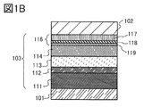

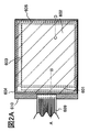


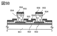
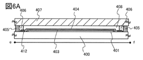
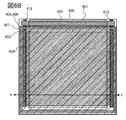


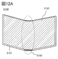
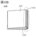


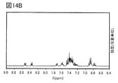


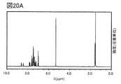


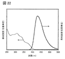


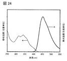


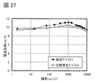

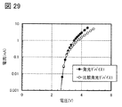


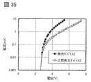

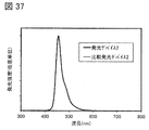


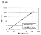


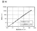


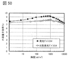


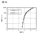


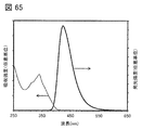


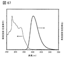


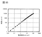


Classifications
-
- C—CHEMISTRY; METALLURGY
- C07—ORGANIC CHEMISTRY
- C07D—HETEROCYCLIC COMPOUNDS
- C07D307/00—Heterocyclic compounds containing five-membered rings having one oxygen atom as the only ring hetero atom
- C07D307/77—Heterocyclic compounds containing five-membered rings having one oxygen atom as the only ring hetero atom ortho- or peri-condensed with carbocyclic rings or ring systems
-
- C—CHEMISTRY; METALLURGY
- C07—ORGANIC CHEMISTRY
- C07D—HETEROCYCLIC COMPOUNDS
- C07D209/00—Heterocyclic compounds containing five-membered rings, condensed with other rings, with one nitrogen atom as the only ring hetero atom
- C07D209/56—Ring systems containing three or more rings
- C07D209/80—[b, c]- or [b, d]-condensed
- C07D209/82—Carbazoles; Hydrogenated carbazoles
- C07D209/86—Carbazoles; Hydrogenated carbazoles with only hydrogen atoms, hydrocarbon or substituted hydrocarbon radicals, directly attached to carbon atoms of the ring system
-
- C—CHEMISTRY; METALLURGY
- C07—ORGANIC CHEMISTRY
- C07D—HETEROCYCLIC COMPOUNDS
- C07D307/00—Heterocyclic compounds containing five-membered rings having one oxygen atom as the only ring hetero atom
- C07D307/77—Heterocyclic compounds containing five-membered rings having one oxygen atom as the only ring hetero atom ortho- or peri-condensed with carbocyclic rings or ring systems
- C07D307/91—Dibenzofurans; Hydrogenated dibenzofurans
-
- C—CHEMISTRY; METALLURGY
- C07—ORGANIC CHEMISTRY
- C07D—HETEROCYCLIC COMPOUNDS
- C07D333/00—Heterocyclic compounds containing five-membered rings having one sulfur atom as the only ring hetero atom
- C07D333/50—Heterocyclic compounds containing five-membered rings having one sulfur atom as the only ring hetero atom condensed with carbocyclic rings or ring systems
-
- C—CHEMISTRY; METALLURGY
- C07—ORGANIC CHEMISTRY
- C07D—HETEROCYCLIC COMPOUNDS
- C07D409/00—Heterocyclic compounds containing two or more hetero rings, at least one ring having sulfur atoms as the only ring hetero atoms
- C07D409/02—Heterocyclic compounds containing two or more hetero rings, at least one ring having sulfur atoms as the only ring hetero atoms containing two hetero rings
- C07D409/10—Heterocyclic compounds containing two or more hetero rings, at least one ring having sulfur atoms as the only ring hetero atoms containing two hetero rings linked by a carbon chain containing aromatic rings
-
- C—CHEMISTRY; METALLURGY
- C07—ORGANIC CHEMISTRY
- C07D—HETEROCYCLIC COMPOUNDS
- C07D471/00—Heterocyclic compounds containing nitrogen atoms as the only ring hetero atoms in the condensed system, at least one ring being a six-membered ring with one nitrogen atom, not provided for by groups C07D451/00 - C07D463/00
- C07D471/02—Heterocyclic compounds containing nitrogen atoms as the only ring hetero atoms in the condensed system, at least one ring being a six-membered ring with one nitrogen atom, not provided for by groups C07D451/00 - C07D463/00 in which the condensed system contains two hetero rings
- C07D471/04—Ortho-condensed systems
-
- C—CHEMISTRY; METALLURGY
- C09—DYES; PAINTS; POLISHES; NATURAL RESINS; ADHESIVES; COMPOSITIONS NOT OTHERWISE PROVIDED FOR; APPLICATIONS OF MATERIALS NOT OTHERWISE PROVIDED FOR
- C09K—MATERIALS FOR MISCELLANEOUS APPLICATIONS, NOT PROVIDED FOR ELSEWHERE
- C09K11/00—Luminescent, e.g. electroluminescent, chemiluminescent materials
- C09K11/06—Luminescent, e.g. electroluminescent, chemiluminescent materials containing organic luminescent materials
-
- F—MECHANICAL ENGINEERING; LIGHTING; HEATING; WEAPONS; BLASTING
- F21—LIGHTING
- F21V—FUNCTIONAL FEATURES OR DETAILS OF LIGHTING DEVICES OR SYSTEMS THEREOF; STRUCTURAL COMBINATIONS OF LIGHTING DEVICES WITH OTHER ARTICLES, NOT OTHERWISE PROVIDED FOR
- F21V31/00—Gas-tight or water-tight arrangements
- F21V31/005—Sealing arrangements therefor
-
- H—ELECTRICITY
- H10—SEMICONDUCTOR DEVICES; ELECTRIC SOLID-STATE DEVICES NOT OTHERWISE PROVIDED FOR
- H10K—ORGANIC ELECTRIC SOLID-STATE DEVICES
- H10K50/00—Organic light-emitting devices
- H10K50/10—OLEDs or polymer light-emitting diodes [PLED]
- H10K50/11—OLEDs or polymer light-emitting diodes [PLED] characterised by the electroluminescent [EL] layers
-
- H—ELECTRICITY
- H10—SEMICONDUCTOR DEVICES; ELECTRIC SOLID-STATE DEVICES NOT OTHERWISE PROVIDED FOR
- H10K—ORGANIC ELECTRIC SOLID-STATE DEVICES
- H10K50/00—Organic light-emitting devices
- H10K50/10—OLEDs or polymer light-emitting diodes [PLED]
- H10K50/14—Carrier transporting layers
- H10K50/15—Hole transporting layers
-
- H—ELECTRICITY
- H10—SEMICONDUCTOR DEVICES; ELECTRIC SOLID-STATE DEVICES NOT OTHERWISE PROVIDED FOR
- H10K—ORGANIC ELECTRIC SOLID-STATE DEVICES
- H10K50/00—Organic light-emitting devices
- H10K50/10—OLEDs or polymer light-emitting diodes [PLED]
- H10K50/14—Carrier transporting layers
- H10K50/16—Electron transporting layers
-
- H—ELECTRICITY
- H10—SEMICONDUCTOR DEVICES; ELECTRIC SOLID-STATE DEVICES NOT OTHERWISE PROVIDED FOR
- H10K—ORGANIC ELECTRIC SOLID-STATE DEVICES
- H10K85/00—Organic materials used in the body or electrodes of devices covered by this subclass
- H10K85/60—Organic compounds having low molecular weight
- H10K85/615—Polycyclic condensed aromatic hydrocarbons, e.g. anthracene
-
- H—ELECTRICITY
- H10—SEMICONDUCTOR DEVICES; ELECTRIC SOLID-STATE DEVICES NOT OTHERWISE PROVIDED FOR
- H10K—ORGANIC ELECTRIC SOLID-STATE DEVICES
- H10K85/00—Organic materials used in the body or electrodes of devices covered by this subclass
- H10K85/60—Organic compounds having low molecular weight
- H10K85/631—Amine compounds having at least two aryl rest on at least one amine-nitrogen atom, e.g. triphenylamine
- H10K85/633—Amine compounds having at least two aryl rest on at least one amine-nitrogen atom, e.g. triphenylamine comprising polycyclic condensed aromatic hydrocarbons as substituents on the nitrogen atom
-
- H—ELECTRICITY
- H10—SEMICONDUCTOR DEVICES; ELECTRIC SOLID-STATE DEVICES NOT OTHERWISE PROVIDED FOR
- H10K—ORGANIC ELECTRIC SOLID-STATE DEVICES
- H10K85/00—Organic materials used in the body or electrodes of devices covered by this subclass
- H10K85/60—Organic compounds having low molecular weight
- H10K85/631—Amine compounds having at least two aryl rest on at least one amine-nitrogen atom, e.g. triphenylamine
- H10K85/636—Amine compounds having at least two aryl rest on at least one amine-nitrogen atom, e.g. triphenylamine comprising heteroaromatic hydrocarbons as substituents on the nitrogen atom
-
- H—ELECTRICITY
- H10—SEMICONDUCTOR DEVICES; ELECTRIC SOLID-STATE DEVICES NOT OTHERWISE PROVIDED FOR
- H10K—ORGANIC ELECTRIC SOLID-STATE DEVICES
- H10K85/00—Organic materials used in the body or electrodes of devices covered by this subclass
- H10K85/60—Organic compounds having low molecular weight
- H10K85/649—Aromatic compounds comprising a hetero atom
- H10K85/654—Aromatic compounds comprising a hetero atom comprising only nitrogen as heteroatom
-
- H—ELECTRICITY
- H10—SEMICONDUCTOR DEVICES; ELECTRIC SOLID-STATE DEVICES NOT OTHERWISE PROVIDED FOR
- H10K—ORGANIC ELECTRIC SOLID-STATE DEVICES
- H10K85/00—Organic materials used in the body or electrodes of devices covered by this subclass
- H10K85/60—Organic compounds having low molecular weight
- H10K85/649—Aromatic compounds comprising a hetero atom
- H10K85/657—Polycyclic condensed heteroaromatic hydrocarbons
- H10K85/6572—Polycyclic condensed heteroaromatic hydrocarbons comprising only nitrogen in the heteroaromatic polycondensed ring system, e.g. phenanthroline or carbazole
-
- H—ELECTRICITY
- H10—SEMICONDUCTOR DEVICES; ELECTRIC SOLID-STATE DEVICES NOT OTHERWISE PROVIDED FOR
- H10K—ORGANIC ELECTRIC SOLID-STATE DEVICES
- H10K85/00—Organic materials used in the body or electrodes of devices covered by this subclass
- H10K85/60—Organic compounds having low molecular weight
- H10K85/649—Aromatic compounds comprising a hetero atom
- H10K85/657—Polycyclic condensed heteroaromatic hydrocarbons
- H10K85/6574—Polycyclic condensed heteroaromatic hydrocarbons comprising only oxygen in the heteroaromatic polycondensed ring system, e.g. cumarine dyes
-
- H—ELECTRICITY
- H10—SEMICONDUCTOR DEVICES; ELECTRIC SOLID-STATE DEVICES NOT OTHERWISE PROVIDED FOR
- H10K—ORGANIC ELECTRIC SOLID-STATE DEVICES
- H10K85/00—Organic materials used in the body or electrodes of devices covered by this subclass
- H10K85/60—Organic compounds having low molecular weight
- H10K85/649—Aromatic compounds comprising a hetero atom
- H10K85/657—Polycyclic condensed heteroaromatic hydrocarbons
- H10K85/6576—Polycyclic condensed heteroaromatic hydrocarbons comprising only sulfur in the heteroaromatic polycondensed ring system, e.g. benzothiophene
-
- C—CHEMISTRY; METALLURGY
- C09—DYES; PAINTS; POLISHES; NATURAL RESINS; ADHESIVES; COMPOSITIONS NOT OTHERWISE PROVIDED FOR; APPLICATIONS OF MATERIALS NOT OTHERWISE PROVIDED FOR
- C09K—MATERIALS FOR MISCELLANEOUS APPLICATIONS, NOT PROVIDED FOR ELSEWHERE
- C09K2211/00—Chemical nature of organic luminescent or tenebrescent compounds
- C09K2211/10—Non-macromolecular compounds
- C09K2211/1003—Carbocyclic compounds
- C09K2211/1011—Condensed systems
-
- C—CHEMISTRY; METALLURGY
- C09—DYES; PAINTS; POLISHES; NATURAL RESINS; ADHESIVES; COMPOSITIONS NOT OTHERWISE PROVIDED FOR; APPLICATIONS OF MATERIALS NOT OTHERWISE PROVIDED FOR
- C09K—MATERIALS FOR MISCELLANEOUS APPLICATIONS, NOT PROVIDED FOR ELSEWHERE
- C09K2211/00—Chemical nature of organic luminescent or tenebrescent compounds
- C09K2211/10—Non-macromolecular compounds
- C09K2211/1003—Carbocyclic compounds
- C09K2211/1014—Carbocyclic compounds bridged by heteroatoms, e.g. N, P, Si or B
-
- C—CHEMISTRY; METALLURGY
- C09—DYES; PAINTS; POLISHES; NATURAL RESINS; ADHESIVES; COMPOSITIONS NOT OTHERWISE PROVIDED FOR; APPLICATIONS OF MATERIALS NOT OTHERWISE PROVIDED FOR
- C09K—MATERIALS FOR MISCELLANEOUS APPLICATIONS, NOT PROVIDED FOR ELSEWHERE
- C09K2211/00—Chemical nature of organic luminescent or tenebrescent compounds
- C09K2211/10—Non-macromolecular compounds
- C09K2211/1018—Heterocyclic compounds
- C09K2211/1025—Heterocyclic compounds characterised by ligands
- C09K2211/1088—Heterocyclic compounds characterised by ligands containing oxygen as the only heteroatom
-
- H—ELECTRICITY
- H10—SEMICONDUCTOR DEVICES; ELECTRIC SOLID-STATE DEVICES NOT OTHERWISE PROVIDED FOR
- H10K—ORGANIC ELECTRIC SOLID-STATE DEVICES
- H10K50/00—Organic light-emitting devices
- H10K50/10—OLEDs or polymer light-emitting diodes [PLED]
- H10K50/14—Carrier transporting layers
- H10K50/15—Hole transporting layers
- H10K50/156—Hole transporting layers comprising a multilayered structure
-
- H—ELECTRICITY
- H10—SEMICONDUCTOR DEVICES; ELECTRIC SOLID-STATE DEVICES NOT OTHERWISE PROVIDED FOR
- H10K—ORGANIC ELECTRIC SOLID-STATE DEVICES
- H10K50/00—Organic light-emitting devices
- H10K50/10—OLEDs or polymer light-emitting diodes [PLED]
- H10K50/17—Carrier injection layers
-
- H—ELECTRICITY
- H10—SEMICONDUCTOR DEVICES; ELECTRIC SOLID-STATE DEVICES NOT OTHERWISE PROVIDED FOR
- H10K—ORGANIC ELECTRIC SOLID-STATE DEVICES
- H10K59/00—Integrated devices, or assemblies of multiple devices, comprising at least one organic light-emitting element covered by group H10K50/00
- H10K59/10—OLED displays
- H10K59/12—Active-matrix OLED [AMOLED] displays
Landscapes
- Chemical & Material Sciences (AREA)
- Organic Chemistry (AREA)
- Engineering & Computer Science (AREA)
- Materials Engineering (AREA)
- Physics & Mathematics (AREA)
- Spectroscopy & Molecular Physics (AREA)
- Optics & Photonics (AREA)
- General Engineering & Computer Science (AREA)
- Electroluminescent Light Sources (AREA)
- Organic Low-Molecular-Weight Compounds And Preparation Thereof (AREA)
Abstract
Description


図2Aおよび図2Bはアクティブマトリクス型発光装置の概念図である。
図3Aおよび図3Bはアクティブマトリクス型発光装置の概念図である。
図4はアクティブマトリクス型発光装置の概念図である。
図5Aおよび図5Bはパッシブマトリクス型発光装置の概念図である。
図6Aおよび図6Bは照明装置を表す図である。
図7A、図7B1、図7B2および図7Cは電子機器を表す図である。
図8A、図8Bおよび図8Cは電子機器を表す図である。
図9は照明装置を表す図である。
図10は照明装置を表す図である。
図11は車載表示装置及び照明装置を表す図である。
図12Aおよび図12Bは電子機器を表す図である。
図13A、図13Bおよび図13Cは電子機器を表す図である。
図14Aおよび図14BはoFBiBnf(6)の1H NMRチャートである。
図15はoFBiBnf(6)のトルエン溶液における吸収スペクトルと発光スペクトルである。
図16はoFBiBnf(6)の薄膜状態における吸収スペクトルと発光スペクトルである。
図17Aおよび図17BはoFBi(4)Bnf(6)の1H NMRチャートである。
図18はoFBi(4)Bnf(6)のトルエン溶液における吸収スペクトルと発光スペクトルである。
図19はoFBi(4)Bnf(6)の薄膜状態における吸収スペクトルと発光スペクトルである。
図20Aおよび図20BはFBi(4)Bnf(6)の1H NMRチャートである。
図21はFBi(4)Bnf(6)のトルエン溶液における吸収スペクトルと発光スペクトルである。
図22はFBi(4)Bnf(6)の薄膜状態における吸収スペクトルと発光スペクトルである。
図23Aおよび図23BはFBiBnf(6)の1H NMRチャートである。
図24はFBiBnf(6)のトルエン溶液における吸収スペクトルと発光スペクトルである。
図25はFBiBnf(6)の薄膜状態における吸収スペクトルと発光スペクトルである。
図26は発光デバイス1及び比較発光デバイス1の輝度−電流密度特性である。
図27は発光デバイス1及び比較発光デバイス1の電流効率−輝度特性である。
図28は発光デバイス1及び比較発光デバイス1の輝度−電圧特性である。
図29は発光デバイス1及び比較発光デバイス1の電流−電圧特性である。
図30は発光デバイス1及び比較発光デバイス1の外部量子効率−輝度特性である。
図31は発光デバイス1及び比較発光デバイス1の発光スペクトルである。
図32は発光デバイス2及び比較発光デバイス2の輝度−電流密度特性である。
図33は発光デバイス2及び比較発光デバイス2の電流効率−輝度特性である。
図34は発光デバイス2及び比較発光デバイス2の輝度−電圧特性である。
図35は発光デバイス2及び比較発光デバイス2の電流−電圧特性である。
図36は発光デバイス2及び比較発光デバイス2の外部量子効率−輝度特性である。
図37は発光デバイス2及び比較発光デバイス2の発光スペクトルである。
図38は発光デバイス1及び比較発光デバイス1の規格化輝度−時間変化特性である。
図39は発光デバイス2及び比較発光デバイス2の規格化輝度−時間変化特性である。
図40は発光デバイス3及び比較発光デバイス3の輝度−電流密度特性である。
図41は発光デバイス3及び比較発光デバイス3の電流効率−輝度特性である。
図42は発光デバイス3及び比較発光デバイス3の輝度−電圧特性である。
図43は発光デバイス3及び比較発光デバイス3の電流−電圧特性である。
図44は発光デバイス3及び比較発光デバイス3の外部量子効率−輝度特性である。
図45は発光デバイス3及び比較発光デバイス3の発光スペクトルである。
図46は発光デバイス4及び比較発光デバイス4の輝度−電流密度特性である。
図47は発光デバイス4及び比較発光デバイス4の電流効率−輝度特性である。
図48は発光デバイス4及び比較発光デバイス4の輝度−電圧特性である。
図49は発光デバイス4及び比較発光デバイス4の電流−電圧特性である。
図50は発光デバイス4及び比較発光デバイス4の外部量子効率−輝度特性である。
図51は発光デバイス4及び比較発光デバイス4の発光スペクトルである。
図52は発光デバイス3及び比較発光デバイス3の規格化輝度−時間変化特性である。
図53は発光デバイス4及び比較発光デバイス4の規格化輝度−時間変化特性である。
図54は発光デバイス5及び発光デバイス6の輝度−電流密度特性である。
図55は発光デバイス5及び発光デバイス6の電流効率−輝度特性である。
図56は発光デバイス5及び発光デバイス6の輝度−電圧特性である。
図57は発光デバイス5及び発光デバイス6の電流−電圧特性である。
図58は発光デバイス5及び発光デバイス6の外部量子効率−輝度特性である。
図59は発光デバイス5及び発光デバイス6の発光スペクトルである。
図60Aおよび図60BはFBiBnf(8)の1H NMRチャートである。
図61はFBiBnf(8)のトルエン溶液における吸収スペクトルと発光スペクトルである。
図62はFBiBnf(8)の薄膜状態における吸収スペクトルと発光スペクトルである。
図63Aおよび図63BはoFBiBnf(8)の1H NMRチャートである。
図64はoFBiBnf(8)のトルエン溶液における吸収スペクトルと発光スペクトルである。
図65はoFBiBnf(8)の薄膜状態における吸収スペクトルと発光スペクトルである。
図66Aおよび図66BはFBi(4)Bnf(8)の1H NMRチャートである。
図67はFBi(4)Bnf(8)のトルエン溶液における吸収スペクトルと発光スペクトルである。
図68はFBi(4)Bnf(8)の薄膜状態における吸収スペクトルと発光スペクトルである。
図69はoFBi(4)Bnf(8)のトルエン溶液における吸収スペクトルと発光スペクトルである。
図70はoFBi(4)Bnf(8)の薄膜状態における吸収スペクトルと発光スペクトルである。
図71は発光デバイス7及び発光デバイス8の輝度−電流密度特性である。
図72は発光デバイス7及び発光デバイス8の電流効率−輝度特性である。
図73は発光デバイス7及び発光デバイス8の輝度−電圧特性である。
図74は発光デバイス7及び発光デバイス8の電流−電圧特性である。
図75は発光デバイス7及び発光デバイス8の外部量子効率−輝度特性である。
図76は発光デバイス7及び発光デバイス8の発光スペクトルである。
図77は発光デバイス7及び発光デバイス8の規格化輝度−時間変化特性である。
図78は発光デバイス9及び比較発光デバイス5の輝度−電流密度特性である。
図79は発光デバイス9及び比較発光デバイス5の電流効率−輝度特性である。
図80は発光デバイス9及び比較発光デバイス5の輝度−電圧特性である。
図81は発光デバイス9及び比較発光デバイス5の電流−電圧特性である。
図82は発光デバイス9及び比較発光デバイス5の外部量子効率−輝度特性である。
図83は発光デバイス9及び比較発光デバイス5の発光スペクトルである。
図84は発光デバイス9及び比較発光デバイス5の規格化輝度−時間変化特性である。
図85は発光デバイス10の輝度−電流密度特性である。
図86は発光デバイス10の電流効率−輝度特性である。
図87は発光デバイス10の輝度−電圧特性である。
図88は発光デバイス10の電流−電圧特性である。
図89は発光デバイス10の外部量子効率−輝度特性である。
図90は発光デバイス10の発光スペクトルである。 1A, 1B and 1C are schematic views of the light emitting device.
2A and 2B are conceptual diagrams of an active matrix type light emitting device.
3A and 3B are conceptual diagrams of an active matrix type light emitting device.
FIG. 4 is a conceptual diagram of an active matrix type light emitting device.
5A and 5B are conceptual diagrams of a passive matrix type light emitting device.
6A and 6B are diagrams showing a lighting device.
7A, 7B1, 7B2 and 7C are diagrams representing electronic devices.
8A, 8B and 8C are diagrams representing electronic devices.
FIG. 9 is a diagram showing a lighting device.
FIG. 10 is a diagram showing a lighting device.
FIG. 11 is a diagram showing an in-vehicle display device and a lighting device.
12A and 12B are diagrams representing electronic devices.
13A, 13B and 13C are diagrams representing electronic devices.
14A and 14B are 1 1 H NMR charts of oFBiBnf (6).
FIG. 15 shows an absorption spectrum and an emission spectrum of oFBiBnf (6) in a toluene solution.
FIG. 16 shows an absorption spectrum and an emission spectrum of oFBiBnf (6) in a thin film state.
17A and 17B are 1 1 H NMR charts of oFBi (4) Bnf (6).
FIG. 18 shows an absorption spectrum and an emission spectrum of oFBi (4) Bnf (6) in a toluene solution.
FIG. 19 shows an absorption spectrum and an emission spectrum of oFBi (4) Bnf (6) in a thin film state.
20A and 20B are 1 1 H NMR charts of FBi (4) Bnf (6).
FIG. 21 shows an absorption spectrum and an emission spectrum of FBi (4) Bnf (6) in a toluene solution.
FIG. 22 shows an absorption spectrum and an emission spectrum of FBi (4) Bnf (6) in a thin film state.
23A and 23B are 1 H NMR charts of FBiBnf (6).
FIG. 24 shows an absorption spectrum and an emission spectrum of FBiBnf (6) in a toluene solution.
FIG. 25 shows an absorption spectrum and an emission spectrum of FBiBnf (6) in a thin film state.
FIG. 26 shows the brightness-current density characteristics of the
FIG. 27 shows the current efficiency-luminance characteristics of the
FIG. 28 shows the luminance-voltage characteristics of the
FIG. 29 shows the current-voltage characteristics of the
FIG. 30 shows the external quantum efficiency-luminance characteristics of the
FIG. 31 is an emission spectrum of the
FIG. 32 shows the brightness-current density characteristics of the
FIG. 33 shows the current efficiency-luminance characteristics of the
FIG. 34 shows the luminance-voltage characteristics of the
FIG. 35 shows the current-voltage characteristics of the
FIG. 36 shows the external quantum efficiency-luminance characteristics of the
FIG. 37 is an emission spectrum of the
FIG. 38 shows the normalized luminance-time change characteristics of the
FIG. 39 shows the normalized luminance-time change characteristics of the
FIG. 40 shows the brightness-current density characteristics of the
FIG. 41 shows the current efficiency-luminance characteristics of the
FIG. 42 shows the luminance-voltage characteristics of the
FIG. 43 shows the current-voltage characteristics of the
FIG. 44 shows the external quantum efficiency-luminance characteristics of the
FIG. 45 is an emission spectrum of the
FIG. 46 shows the brightness-current density characteristics of the
FIG. 47 shows the current efficiency-luminance characteristics of the
FIG. 48 shows the luminance-voltage characteristics of the
FIG. 49 shows the current-voltage characteristics of the
FIG. 50 shows the external quantum efficiency-luminance characteristics of the
FIG. 51 is an emission spectrum of the
FIG. 52 shows the normalized luminance-time change characteristics of the
FIG. 53 shows the normalized luminance-time change characteristics of the
FIG. 54 shows the brightness-current density characteristics of the
FIG. 55 shows the current efficiency-luminance characteristics of the
FIG. 56 shows the luminance-voltage characteristics of the
FIG. 57 shows the current-voltage characteristics of the
FIG. 58 shows the external quantum efficiency-luminance characteristics of the
FIG. 59 is an emission spectrum of the
60A and 60B are 1 H NMR charts of FBiBnf (8).
FIG. 61 shows an absorption spectrum and an emission spectrum of FBiBnf (8) in a toluene solution.
FIG. 62 shows an absorption spectrum and an emission spectrum of FBiBnf (8) in a thin film state.
63A and 63B are 1 1 H NMR charts of oFBiBnf (8).
FIG. 64 shows an absorption spectrum and an emission spectrum of oFBiBnf (8) in a toluene solution.
FIG. 65 shows an absorption spectrum and an emission spectrum of oFBiBnf (8) in a thin film state.
66A and 66B are 1 1 H NMR charts of FBi (4) Bnf (8).
FIG. 67 shows an absorption spectrum and an emission spectrum of FBi (4) Bnf (8) in a toluene solution.
FIG. 68 shows an absorption spectrum and an emission spectrum of FBi (4) Bnf (8) in a thin film state.
FIG. 69 shows an absorption spectrum and an emission spectrum of oFBi (4) Bnf (8) in a toluene solution.
FIG. 70 shows the absorption spectrum and the emission spectrum of oFBi (4) Bnf (8) in the thin film state.
FIG. 71 shows the brightness-current density characteristics of the
FIG. 72 shows the current efficiency-luminance characteristics of the
FIG. 73 shows the luminance-voltage characteristics of the
FIG. 74 shows the current-voltage characteristics of the
FIG. 75 shows the external quantum efficiency-luminance characteristics of the
FIG. 76 is an emission spectrum of the
FIG. 77 shows the normalized luminance-time change characteristics of the
FIG. 78 shows the brightness-current density characteristics of the
FIG. 79 shows the current efficiency-luminance characteristics of the
FIG. 80 shows the luminance-voltage characteristics of the
FIG. 81 shows the current-voltage characteristics of the
FIG. 82 shows the external quantum efficiency-luminance characteristics of the
FIG. 83 is an emission spectrum of the
FIG. 84 shows the normalized luminance-time change characteristics of the
FIG. 85 shows the brightness-current density characteristics of the
FIG. 86 shows the current efficiency-luminance characteristics of the
FIG. 87 shows the luminance-voltage characteristics of the
FIG. 88 shows the current-voltage characteristics of the
FIG. 89 shows the external quantum efficiency-luminance characteristic of the
FIG. 90 is an emission spectrum of the
本実施の形態では、本発明の一態様の有機化合物について説明する。 (Embodiment 1)
In the present embodiment, the organic compound of one aspect of the present invention will be described.


本実施の形態では、本発明の一態様の発光デバイスについて説明する。 (Embodiment 2)
In the present embodiment, the light emitting device of one aspect of the present invention will be described.


これら導電性材料は、真空蒸着法やスパッタリング法などの乾式法、インクジェット法、スピンコート法等を用いて成膜することが可能である。また、ゾル−ゲル法を用いて湿式法で形成しても良いし、金属材料のペーストを用いて湿式法で形成してもよい。 As the substance forming the
These conductive materials can be formed into a film by using a dry method such as a vacuum vapor deposition method or a sputtering method, an inkjet method, a spin coating method, or the like. Further, it may be formed by a wet method using a sol-gel method, or may be formed by a wet method using a paste of a metal material.
本実施の形態では、実施の形態2に記載の発光デバイスを用いた発光装置について説明する。 (Embodiment 3)
In this embodiment, a light emitting device using the light emitting device according to the second embodiment will be described.
本実施の形態では、実施の形態2に記載の発光デバイスを照明装置として用いる例を図6を参照しながら説明する。図6Bは照明装置の上面図、図6Aは図6Bにおけるe−f断面図である。 (Embodiment 4)
In the present embodiment, an example in which the light emitting device according to the second embodiment is used as a lighting device will be described with reference to FIG. FIG. 6B is a top view of the lighting device, and FIG. 6A is a cross-sectional view taken along the line ef in FIG. 6B.
本実施の形態では、実施の形態2に記載の発光デバイスをその一部に含む電子機器の例について説明する。実施の形態2に記載の発光デバイスは発光効率が良好であり、消費電力の小さい発光デバイスである。その結果、本実施の形態に記載の電子機器は、消費電力が小さい発光部を有する電子機器とすることが可能である。 (Embodiment 5)
In the present embodiment, an example of an electronic device including the light emitting device according to the second embodiment as a part thereof will be described. The light emitting device according to the second embodiment is a light emitting device having good luminous efficiency and low power consumption. As a result, the electronic device described in the present embodiment can be an electronic device having a light emitting unit having low power consumption.
本合成例では、実施の形態1で構造式(5−106)として示したN−(1,1’−ビフェニル−2−イル)−N−(9,9−ジメチル−9H−フルオレン−2−イル)ベンゾ[b]ナフト[1,2−d]フラン−6−アミン(略称:oFBiBnf(6))の合成方法について説明する。oFBiBnf(6)の構造式を以下に示す。 << Synthesis example 1 >>
In this synthetic example, N- (1,1'-biphenyl-2-yl) -N- (9,9-dimethyl-9H-fluorene-2-) represented by the structural formula (5-106) in the first embodiment Il) A method for synthesizing benzo [b] naphtho [1,2-d] furan-6-amine (abbreviation: oFBiBnf (6)) will be described. The structural formula of oFBiBnf (6) is shown below.

5.2g(15mmol)の6−ヨード−ベンゾ[b]ナフト[1,2−d]フランと、2.5g(15mmol)の2−ビフェニルアミンと、0.12g(0.30mmol)の2−ジシクロヘキシルホスフィノ−2’,6’−ジメトキシビフェニルを、還流管を付けた200mL三口フラスコに入れ、フラスコ内を窒素置換した。フラスコ内に2.9g(30mmol)のナトリウム tert−ブトキシドと、110mLのキシレンを加え、減圧脱気と窒素置換を3回ずつ行った。フラスコ内に86mg(0.15mmol)のビス(ビス(ジベンジリデンアセトン)パラジウム)(0)を加え、110℃で3時間攪拌した。攪拌後、吸引濾過により得られた混合物から不溶物を除去した。得られたろ液に水を加え、水層をトルエンで抽出した。得られた有機層を水で2回洗浄した後飽和食塩水で洗浄し、無水硫酸マグネシウムで乾燥した。得られた混合物を自然ろ過し、無水硫酸マグネシウムを除去した。得られたろ液を濃縮し、目的物の褐色固体を5.5g、収率95%で得た。ステップ1の合成スキームを以下に示す。 <Step 1: Synthesis of N- (1,1'-biphenyl-2-yl) benzo [b] naphtho [1,2-d] furan-6-amine>
5.2 g (15 mmol) of 6-iodo-benzo [b] naphtho [1,2-d] flask, 2.5 g (15 mmol) of 2-biphenylamine, and 0.12 g (0.30 mmol) of 2- Dicyclohexylphosphino-2', 6'-dimethoxybiphenyl was placed in a 200 mL three-necked flask equipped with a reflux tube, and the inside of the flask was replaced with nitrogen. 2.9 g (30 mmol) of sodium tert-butoxide and 110 mL of xylene were added to the flask, and vacuum degassing and nitrogen substitution were performed three times each. 86 mg (0.15 mmol) of bis (bis (dibenzylideneacetone) palladium) (0) was added to the flask, and the mixture was stirred at 110 ° C. for 3 hours. After stirring, insoluble matter was removed from the mixture obtained by suction filtration. Water was added to the obtained filtrate, and the aqueous layer was extracted with toluene. The obtained organic layer was washed twice with water, washed with saturated brine, and dried over anhydrous magnesium sulfate. The resulting mixture was naturally filtered to remove anhydrous magnesium sulfate. The obtained filtrate was concentrated to obtain 5.5 g of the desired brown solid in a yield of 95%. The synthesis scheme of

1H NMR(ジクロロメタン−d2,300MHz):δ=8.52(d、J=7.8Hz、1H)、7.91(d、J=8.7Hz、1H)、7.84(d、J=8.4Hz、1H)、7.68−7.32(m、14H)、7.19(t、J=4.2Hz、1H)、6.39(s、1H) The analysis results of the brown solid obtained in
1 H NMR (dichloromethane -d 2, 300MHz): δ = 8.52 (d, J = 7.8Hz, 1H), 7.91 (d, J = 8.7Hz, 1H), 7.84 (d, J = 8.4Hz, 1H), 7.68-7.32 (m, 14H), 7.19 (t, J = 4.2Hz, 1H), 6.39 (s, 1H)
2.0g(5.2mmol)のステップ1で得られたN−(1,1’−ビフェニル−2−イル)ベンゾ[b]ナフト[1,2−d]フラン−6−アミンと、1.4g(5.2mmol)の2−ブロモ−9,9−ジメチルフルオレンを、還流管を付けた200mL三口フラスコに入れ、フラスコ内を窒素置換した。フラスコ内に1.0g(10mmol)のナトリウム tert−ブトキシドと、0.30mLのトリ−tert−ブチルホスフィン(10wt%ヘキサン溶液)と、50mLのキシレンを加え、減圧脱気と窒素置換を3回ずつ行なった。フラスコ内に30mg(0.51mmol)のビス(ビス(ジベンジリデンアセトン)パラジウム)(0)を加え、90℃で6時間攪拌した。攪拌後、反応物に水を加え、水層をトルエンで抽出した。得られた有機層を水で2回洗浄し、続いて飽和食塩水で洗浄した後、無水硫酸マグネシウムで乾燥した。得られた混合物を自然ろ過し、無水硫酸マグネシウムを除去した。得られたろ液を濃縮したところ、目的物が含まれる黄色固体を2.9g、収率96%で得た。 <Step 2: N- (1,1'-biphenyl-2-yl) -N- (9,9-dimethyl-9H-fluorene-2-yl) benzo [b] naphtho [1,2-d] furan- Synthesis of 6-amine (abbreviation: oFBiBnf (6))>
2. 2.0 g (5.2 mmol) of N- (1,1'-biphenyl-2-yl) benzo [b] naphtho [1,2-d] furan-6-amine obtained in

1H NMR(ジクロロメタン−d2,300MHz):δ=8.53(d、J=8.4Hz、1H)、8.38−8.34(m、1H)、7.73(d、J=8.4Hz、1H)、7.58(t、J=6.6Hz、2H)、7.48−7.20(m、15H)、6.91−6.85(m、4H)、6.77(t、J=7.5Hz、1H)、1.24(s、6H) The numerical data of 1 H-NMR of the obtained solid is shown below. 1 H-NMR charts are shown in FIGS. 14A and 14B. From this, it was found that oFBiBnf (6) was obtained by this synthetic example.
1 H NMR (dichloromethane -d 2, 300MHz): δ = 8.53 (d, J = 8.4Hz, 1H), 8.38-8.34 (m, 1H), 7.73 (d, J = 8.4Hz, 1H), 7.58 (t, J = 6.6Hz, 2H), 7.48-7.20 (m, 15H), 6.91-6.85 (m, 4H), 6. 77 (t, J = 7.5Hz, 1H), 1.24 (s, 6H)
[0328]
以上の結果から、本発明の一態様の有機化合物は、高い耐熱性と良好な昇華性を併せ持ち、耐熱性の高い有機光デバイス(発光デバイス及び受光デバイス)を提供でき、また、デバイス作製の生産性を高くできることが確認された。 In addition, differential thermal analysis (Thermogravimetric-Differential Thermal Analysis) of oFBiBnf (6) was performed. A high vacuum differential differential thermal balance (TG-DTA2410SA, manufactured by Bruker AXS Corporation) was used for the measurement. The measurement was carried out at atmospheric pressure under the conditions of a heating rate of 10 ° C./min and a nitrogen stream (flow velocity of 200 mL / min). Thermogravimetric analysis-In differential thermal analysis, it was found that the temperature (decomposition temperature) at which the weight obtained from the thermogravimetric analysis was -5% at the start of measurement was 366 ° C, and the substance had good sublimation properties. It has been shown.
[0328]
From the above results, the organic compound according to one aspect of the present invention can provide an organic optical device (light emitting device and light receiving device) having both high heat resistance and good sublimation property and high heat resistance, and can also be used for production of device fabrication. It was confirmed that the sex can be improved.
本合成例では、実施の形態1で構造式(5−107)として示したN−(1,1’−ビフェニル−2−イル)−N−(9,9−ジメチル−9H−フルオレン−4−イル)ベンゾ[b]ナフト[1,2−d]フラン−6−アミン(略称:oFBi(4)Bnf(6))の合成方法について説明する。oFBi(4)Bnf(6)の構造式を以下に示す。 ≪Synthesis example 2≫
In this synthetic example, N- (1,1'-biphenyl-2-yl) -N- (9,9-dimethyl-9H-fluorene-4-) represented by the structural formula (5-107) in the first embodiment. Il) A method for synthesizing benzo [b] naphtho [1,2-d] furan-6-amine (abbreviation: oFBi (4) Bnf (6)) will be described. The structural formulas of oFBi (4) and Bnf (6) are shown below.

実施例1の合成例1におけるステップ1と同様に合成した。 <Step 1: Synthesis of N- (1,1'-biphenyl-2-yl) benzo [b] naphtho [1,2-d] furan-6-amine>
Synthesis of Example 1 Synthesis was carried out in the same manner as in
2.0g(5.2mmol)のステップ1で得られたN−(1,1’−ビフェニル−2−イル)ベンゾ[b]ナフト[1,2−d]フラン−6−アミンと、1.4g(5.2mmol)の4−ブロモ−9−ジメチルフルオレンを、還流管を付けた200mL三口フラスコに入れ、フラスコ内を窒素置換した。フラスコ内に1.0g(10mmol)のナトリウム tert−ブトキシドと、0.30mLのトリ−tert−ブチルホスフィン(10wt%ヘキサン溶液)と、50mLのキシレンを加え、減圧脱気と窒素置換を3回ずつ行なった。フラスコ内に30mg(0.51mmol)のビス(ビス(ジベンジリデンアセトン)パラジウム)(0)を加え、80℃で16時間攪拌した。攪拌後、反応物に水を加え、水層をトルエンで抽出した。得られた有機層を水で2回洗浄し、続いて飽和食塩水で洗浄した後、無水硫酸マグネシウムで乾燥した。得られた混合物を自然ろ過し、無水硫酸マグネシウムを除去した。得られたろ液を濃縮したところ、目的物が含まれる黄色固体を2.9g得られた。この黄色固体を再結晶(トルエン/ヘキサン)で精製し、目的物の白色固体を1.4g、収率47%で得た。 <Step 2: N- (1,1'-biphenyl-2-yl) -N- (9,9-dimethyl-9H-fluorene-4-yl) benzo [b] naphtho [1,2-d] furan- Synthesis of 6-amine (abbreviation: oFBi (4) Bnf (6))>
2. 2.0 g (5.2 mmol) of N- (1,1'-biphenyl-2-yl) benzo [b] naphtho [1,2-d] furan-6-amine obtained in

1H NMR(ジクロロメタン−d2,300MHz):δ=8.57(d、J=7.8Hz、1H)、8.50−8.44(m、1H)、7.66−7.50(m、5H)、7.42−7.03(m、12H)、6.97(t、J=7.5Hz、1H)、6.83(d、J=7.5Hz、1H)、6.65−6.55(m、4H)、1.29(s、6H) The numerical data of 1 H-NMR of the obtained solid is shown below. 1 H-NMR charts are shown in FIGS. 17A and 17B. As a result, it was found that oFBi (4) Bnf (6) was obtained by this synthetic example.
1 H NMR (dichloromethane -d 2, 300MHz): δ = 8.57 (d, J = 7.8Hz, 1H), 8.50-8.44 (m, 1H), 7.66-7.50 ( m, 5H), 7.42-7.03 (m, 12H), 6.97 (t, J = 7.5Hz, 1H), 6.83 (d, J = 7.5Hz, 1H), 6. 65-6.55 (m, 4H), 1.29 (s, 6H)
本合成例では、実施の形態1で構造式(5−59)として示したN−(1,1’−ビフェニル−4−イル)−N−(9,9−ジメチル−9H−フルオレン−4−イル)ベンゾ[b]ナフト[1,2−d]フラン−6−アミン(略称:FBi(4)Bnf(6))の合成方法について説明する。FBi(4)Bnf(6)の構造式を以下に示す。 << Synthesis example 3 >>
In this synthesis example, N- (1,1'-biphenyl-4-yl) -N- (9,9-dimethyl-9H-fluorene-4-) represented by the structural formula (5-59) in the first embodiment Il) A method for synthesizing benzo [b] naphtho [1,2-d] furan-6-amine (abbreviation: FBi (4) Bnf (6)) will be described. The structural formulas of FBi (4) and Bnf (6) are shown below.

5.4g(20mmol)の4−ブロモ−9,9−ジメチル−9H−フルオレンと、2.3g(20mmol)のカルバミン酸tert−ブチルと、0.23g(0.40mmol)の4,5−ビス(ジフェニルホスフィノ)−9,9−ジメチルキサンテン(略称:キサントホス)と、13g(40mmol)の炭酸セシウムを、還流管を付けた200mL三口フラスコに入れ、フラスコ内を窒素置換した。フラスコ内に100mLの無水1,4−ジオキサンを加えた後、この混合物を減圧脱気した。フラスコ内を窒素気流下にしてから、この混合物を60℃で撹拌し、55mg0.20mmol)の酢酸パラジウム(II)を加えてから、80℃で3時間撹拌した。攪拌後、析出物を吸引ろ過で除去したのち、混合物を500mLの分液ロートを用いて約100mLの水で3回洗浄した。洗浄により得られた水層を約200mLのトルエンで3回抽出し、得られた抽出液と有機層を合わせて、約300mLの飽和食塩水で1回洗浄した。得られた有機層に無水硫酸マグネシウムを加えて1時間放置したのち、自然ろ過した。得られたろ液を濃縮して得た化合物をシリカゲルカラムクロマトグラフィー(展開溶媒:トルエン:酢酸エチル=9:1)で精製したところ、目的物の白色固体を5.5g、収率88%で得た。ステップ1の合成スキームを以下に示す。 <Step 1: Synthesis of N- (9,9-dimethyl-9H-fluorene-4-yl) t-butoxycarbonylamine>
5.4 g (20 mmol) of 4-bromo-9,9-dimethyl-9H-fluorene, 2.3 g (20 mmol) of tert-butyl carbamate, and 0.23 g (0.40 mmol) of 4,5-bis. (Diphenylphosphino) -9,9-dimethylxanthene (abbreviation: xantphos) and 13 g (40 mmol) of cesium carbonate were placed in a 200 mL three-necked flask equipped with a reflux tube, and the inside of the flask was replaced with nitrogen. After adding 100 mL of

5.5g(18mmol)のステップ1で得られたN−(9,9−ジメチル−9H−フルオレン−4−イル)t−ブトキシカルボニルアミンと、100mLのジクロロメタンを、1000mLナスフラスコに入れ、フラスコ内を窒素気流下にした。この溶液に5.2mL(8.1g,71mmol)のトリフルオロ酢酸を滴下ロートより5分かけて滴下したのち、室温で約16時間撹拌した。撹拌後ナスフラスコを氷浴してから、100mLの水酸化カリウム溶液(0.7mmol)を加えて中和した。得られた混合物を、500mL分液ロートを用いて有機相と水相に分け、有機相を約100mLの水で3回洗浄した。洗浄に用いた水を200mLのトルエンで3回抽出し、得られた抽出液と有機相を合わせて約200mLの飽和食塩水で洗浄した。洗浄後得られた有機相に無水硫酸マグネシウムを加えて1時間放置した後、自然ろ過し、得られたろ液を濃縮した。得られた化合物を真空乾燥したところ、目的物の白色固体を3.2g、収率86%で得た。ステップ2の合成スキームを以下に示す。 <Step 2: Synthesis of 9,9-dimethyl-9H-fluorene-4-amine>
5.5 g (18 mmol) of N- (9,9-dimethyl-9H-fluorene-4-yl) t-butoxycarbonylamine obtained in

1.5g(7.2mmol)のステップ2で得られた9,9−ジメチル−9H−フルオレン−4−アミンと、2.5g(7.2mmol)の6−ヨードベンゾ[b]ナフト[1,2−d]フランと、0.18g(0.4mmol)の2−ジシクロヘキシルホスフィノ−2’,6’−ジメトキシビフェニル(sphos)と、1.5g(15mmol)のt−ブトキシナトリウムを、還流管を付けた200mL三口フラスコに入れ、フラスコ内を窒素置換した。フラスコ内に40mLのトルエンを加え、減圧脱気を行った後、フラスコ内を窒素気流下にした。この混合物を60℃で撹拌し、同温度でフラスコ内に0.11g(0.20mmol)のビス(ビス(ジベンジリデンアセトン)パラジウム)(0)を加えた後、80℃で3時間攪拌した。攪拌後、得られた混合物を1Lの分液ロートを用いて約100mLの水で3回洗浄した。洗浄に用いた水を約100mLのトルエンで3回抽出し、得られた抽出液と有機相を合わせて約200mLの飽和食塩水で洗浄した。得られた有機相に無水硫酸マグネシウムを加えて1時間放置したのち、この混合物を自然ろ過し、得られたろ液を濃縮し、濃褐色の化合物を3.5g得た。得られた化合物をシリカゲルカラムクロマトグラフィー(展開溶媒:ヘキサン:トルエン=2:1)により精製したところ、目的物を1.8g、収率59%で得た。ステップ3の合成スキームを以下に示す。 <Step 3: Synthesis of N- (9,9-dimethyl-9H-fluorene-4-yl) benzo [b] naphtho [1,2-d] furan-6-amine>
1.5 g (7.2 mmol) of 9,9-dimethyl-9H-fluoren-4-amine obtained in

1.8g(4.1mmol)のステップ3で得られたN−(9,9−ジメチル−9H−フルオレン−4−イル)ベンゾ[b]ナフト[1,2−d]フラン−6−アミンと、0.96g(4.1mmol)の4−ブロモビフェニルを、還流管を付けた200mL三口フラスコに入れ、フラスコ内を窒素置換した。フラスコ内に0.80g(8.3mmol)のナトリウム tert−ブトキシドと、0.30mLのトリ−tert−ブチルホスフィン(10wt%ヘキサン溶液)と、25mLのキシレンを加え、減圧脱気と窒素置換を3回ずつ行なった。フラスコ内に24mg(0.41mmol)のビス(ビス(ジベンジリデンアセトン)パラジウム)(0)を加え、80℃で4時間攪拌した。攪拌後、反応物に水を加え、水層をトルエンで抽出した。得られた有機層を水で2回洗浄し、続いて飽和食塩水で洗浄した後、無水硫酸マグネシウムで乾燥した。得られた混合物を自然ろ過し、無水硫酸マグネシウムを除去した。得られたろ液を濃縮したところ、淡黄色固体を3.4g得た。得られた淡黄色固体を高速液体クロマトグラフィー(HPLC)(移動相:クロロホルム)により精製したところ、目的物の白色固体を2.2g、収率93%で得た。 <Step 4: N- (1,1'-biphenyl-4-yl) -N- (9,9-dimethyl-9H-fluorene-4-yl) benzo [b] naphtho [1,2-d] furan- Synthesis of 6-amine (abbreviation: FBi (4) Bnf (6))>
With 1.8 g (4.1 mmol) of N- (9,9-dimethyl-9H-fluorene-4-yl) benzo [b] naphtho [1,2-d] furan-6-amine obtained in

1H NMR(ジクロロメタン−d2,300MHz):δ=8.61(d、J=8.4Hz、1H)、8.45−8.42(m、1H)、7.84(d、J=7.8Hz、1H)、7.78(d、J=8.1Hz、1H)、7.66−7.18(m、18H)、7.03−6.96(m、3H)、1.57(s、6H) The numerical data of 1 H-NMR of the obtained solid is shown below. 1 H-NMR charts are shown in FIGS. 20A and 20B. As a result, it was found that FBi (4) Bnf (6) was obtained in this synthetic example.
1 H NMR (dichloromethane -d 2, 300MHz): δ = 8.61 (d, J = 8.4Hz, 1H), 8.45-8.42 (m, 1H), 7.84 (d, J = 7.8Hz, 1H), 7.78 (d, J = 8.1Hz, 1H), 7.66-7.18 (m, 18H), 7.03-6.96 (m, 3H), 1. 57 (s, 6H)
[0328]
以上の結果から、本発明の一態様の有機化合物は、高い耐熱性と良好な昇華性を併せ持ち、耐熱性の高い有機光デバイス(発光デバイス及び受光デバイス)を提供でき、また、デバイス作製の生産性を高くできることが確認された。 In addition, differential thermal analysis (Thermogravimetric-Differential Thermal Analysis) of FBi (4) Bnf (6) was performed. A high vacuum differential differential thermal balance (TG-DTA2410SA, manufactured by Bruker AXS Corporation) was used for the measurement. The measurement was carried out at atmospheric pressure under the conditions of a heating rate of 10 ° C./min and a nitrogen stream (flow velocity of 200 mL / min). Thermogravimetric analysis-In differential thermal analysis, it was found that the temperature (decomposition temperature) at which the weight obtained from the thermogravimetric analysis was -5% at the start of measurement was 390 ° C, and the substance had good sublimation properties. It has been shown.
[0328]
From the above results, the organic compound according to one aspect of the present invention can provide an organic optical device (light emitting device and light receiving device) having both high heat resistance and good sublimation property and high heat resistance, and can also be used for production of device fabrication. It was confirmed that the sex can be improved.
本合成例では、実施の形態1で構造式(5−58)として示したN−(1,1’−ビフェニル−4−イル)−N−(9,9−ジメチル−9H−フルオレン−2−イル)ベンゾ[b]ナフト[1,2−d]フラン−6−アミン(略称:FBiBnf(6))の合成方法について説明する。FBiBnf(6)の構造式を以下に示す。 ≪Synthesis example 4≫
In this synthetic example, N- (1,1'-biphenyl-4-yl) -N- (9,9-dimethyl-9H-fluorene-2-) represented by the structural formula (5-58) in the first embodiment. Il) A method for synthesizing benzo [b] naphtho [1,2-d] furan-6-amine (abbreviation: FBiBnf (6)) will be described. The structural formula of FBiBnf (6) is shown below.

2.1g(10mmol)の9,9−ジメチル−9H−フルオレン−2−アミンと、3.4g(10mmol)の6−ヨードベンゾ[b]ナフト[1,2−d]フランと、0.84mg(0.2mmol)の2−ジシクロヘキシルホスフィノ−2’,6’−ジメトキシビフェニル(sphos)と、2.0g(20mmol)のt−ブトキシナトリウムを、還流管を付けた200mL三口フラスコに入れ、フラスコ内を窒素置換した。フラスコ内に50mLのトルエンを加え、減圧脱気を行った後、フラスコ内を窒素気流下にした。この混合物を60℃で撹拌し、同温度でフラスコ内に60mg(0.11mmol)のビス(ビス(ジベンジリデンアセトン)パラジウム)(0)を加えた後、80℃で7時間攪拌した。攪拌後、得られた混合物に600mLのトルエンを加えて100℃で加熱撹拌をした。この混合物を同温度で、アルミナ、フロリジール(和光純薬工業株式会社、カタログ番号:066−05265)、セライト(和光純薬工業株式会社、カタログ番号:537−02305)を通してろ過した。得られたろ液を濃縮して得た固体を、エタノール300mLで再結晶を行ったところ、目的物の白色固体を2.5g、収率58%で得た。ステップ1の合成スキームを以下に示す。 <Step 1: Synthesis of N- (9,9-dimethyl-9H-fluorene-2-yl) benzo [b] naphtho [1,2-d] furan-6-amine>
2.1 g (10 mmol) of 9,9-dimethyl-9H-fluorene-2-amine and 3.4 g (10 mmol) of 6-iodobenzo [b] naphtho [1,2-d] furan and 0.84 mg ( 0.2 mmol) 2-dicyclohexylphosphino-2', 6'-dimethoxybiphenyl (sphos) and 2.0 g (20 mmol) t-butoxysodium were placed in a 200 mL three-necked flask equipped with a reflux tube and placed in the flask. Was replaced with nitrogen. After adding 50 mL of toluene into the flask and degassing under reduced pressure, the inside of the flask was placed under a nitrogen stream. The mixture was stirred at 60 ° C., 60 mg (0.11 mmol) of bis (bis (dibenzylideneacetone) palladium) (0) was added to the flask at the same temperature, and the mixture was stirred at 80 ° C. for 7 hours. After stirring, 600 mL of toluene was added to the obtained mixture, and the mixture was heated and stirred at 100 ° C. The mixture was filtered through alumina, Florisil (Wako Pure Chemical Industries, Ltd., Catalog No .: 066-05265) and Celite (Wako Pure Chemical Industries, Ltd., Catalog No .: 537-02305) at the same temperature. The solid obtained by concentrating the obtained filtrate was recrystallized from 300 mL of ethanol to obtain 2.5 g of the desired white solid in a yield of 58%. The synthesis scheme of

1.1g(2.5mmol)のステップ1で得たN−(9,9−ジメチル−9H−フルオレン−2−イル)ベンゾ[b]ナフト[1,2−d]フラン−6−アミンと、0.58g(2.5mmol)の4−ブロモビフェニルと、0.86mg(0.2mmol)の2−ジ−tert−ブチルホスフィノ−2’,4’,6’−トリイソプロピルビフェニル(tBuxphos)と、0.52g(5.0mmol)のt−ブトキシナトリウムを、還流管を付けた200mL三口フラスコに入れ、フラスコ内を窒素置換した。フラスコ内に25mLのキシレンを加え、減圧脱気を行った後、フラスコ内を窒素気流下にした。この混合物を80℃で撹拌し、同温度でフラスコ内に62mg(0.11mmol)のビス(ビス(ジベンジリデンアセトン)パラジウム)(0)を加えた後、110℃で5時間攪拌した。攪拌後、得られた混合物に600mLのトルエンを加えて100℃で加熱撹拌をした。この混合物を同温度で、アルミナ、フロリジール(和光純薬工業株式会社、カタログ番号:066−05265)、セライト(和光純薬工業株式会社、カタログ番号:537−02305)を通してろ過した。得られたろ液を濃縮して得た固体を、シリカゲルカラムクロマトグラフィ−(展開溶媒:ヘキサン:トルエン=1:1)で精製した後、高速液体クロマトグラフィー(展開溶媒:クロロホルム)により精製したところ、目的物の淡黄色固体を0.96g、収率66%で得た。 <Step 2: N- (1,1'-biphenyl-4-yl) -N- (9,9-dimethyl-9H-fluorene-2-yl) -benzo [b] naphtho [1,2-d] furan Synthesis of -6-amine (abbreviation: FBiBnf (6))>
1.1 g (2.5 mmol) of N- (9,9-dimethyl-9H-fluoren-2-yl) benzo [b] naphtho [1,2-d] furan-6-amine obtained in

[0328]
以上の結果から、本発明の一態様の有機化合物は、高い耐熱性と良好な昇華性を併せ持ち、耐熱性の高い有機光デバイス(発光デバイス及び受光デバイス)を提供でき、また、デバイス作製の生産性を高くできることが確認された。 In addition, differential thermal analysis (Thermogravimetric-Differential Thermal Analysis) of FBiBnf (6) was performed. A high vacuum differential differential thermal balance (TG-DTA2410SA, manufactured by Bruker AXS Corporation) was used for the measurement. The measurement was carried out at atmospheric pressure under the conditions of a heating rate of 10 ° C./min and a nitrogen stream (flow velocity of 200 mL / min). Thermogravimetric analysis-In differential thermal analysis, it was found that the temperature (decomposition temperature) at which the weight obtained from the thermogravimetric analysis was -5% at the start of measurement was 352 ° C, and the substance had good sublimation properties. It has been shown.
[0328]
From the above results, the organic compound according to one aspect of the present invention can provide an organic optical device (light emitting device and light receiving device) having both high heat resistance and good sublimation property and high heat resistance, and can also be used for production of device fabrication. It was confirmed that the sex can be improved.

まず、ガラス基板上に、酸化珪素を含むインジウム錫酸化物(ITSO)をスパッタリング法にて成膜し、第1の電極101を形成した。なお、その膜厚は70nmとし、電極面積は2mm×2mmとした。 (Method for manufacturing light emitting device 1)
First, indium tin oxide (ITSO) containing silicon oxide was formed on a glass substrate by a sputtering method to form a
比較発光デバイス1は、発光デバイス1におけるFBiBnf(6)を、上記構造式(vii)で表されるN,N−ビス(4−ビフェニル)−6−フェニルベンゾ[b]ナフト[1,2−d]フラン−8−アミン(略称:BBABnf)に変えた他は発光デバイス1と同様に作製した。 (Method for manufacturing comparative light emitting device 1)
In the comparative
発光デバイス2は、発光デバイス1の正孔輸送層におけるFBiBnf(6)の膜厚を20nmから120nmにした他は発光デバイス1と同様に作製した。 (Method of manufacturing the light emitting device 2)
The
比較発光デバイス2は、発光デバイス2におけるFBiBnf(6)を、BBABnfに変えた他は発光デバイス2と同様に作製した。 (Method for manufacturing comparative light emitting device 2)
The comparative


まず、ガラス基板上に、酸化珪素を含むインジウム錫酸化物(ITSO)をスパッタリング法にて成膜し、第1の電極101を形成した。なお、その膜厚は70nmとし、電極面積は2mm×2mmとした。 (Method for manufacturing light emitting device 3)
First, indium tin oxide (ITSO) containing silicon oxide was formed on a glass substrate by a sputtering method to form a
比較発光デバイス3は、発光デバイス3におけるoFBiBnf(6)を、上記構造式(vii)で表されるN,N−ビス(4−ビフェニル)−6−フェニルベンゾ[b]ナフト[1,2−d]フラン−8−アミン(略称:BBABnf)に変えた他は発光デバイス3と同様に作製した。 (Method for manufacturing comparative light emitting device 3)
The comparative
発光デバイス4は、発光デバイス3の正孔輸送層におけるoFBiBnf(6)の膜厚を20nmから120nmにした他は発光デバイス3と同様に作製した。 (Method of manufacturing the light emitting device 4)
The
比較発光デバイス4は、発光デバイス4におけるoFBiBnf(6)を、BBABnfに変えた他は発光デバイス4と同様に作製した。 (Method for manufacturing comparative light emitting device 4)
The comparative


まず、ガラス基板上に、酸化珪素を含むインジウム錫酸化物(ITSO)をスパッタリング法にて成膜し、第1の電極101を形成した。なお、その膜厚は70nmとし、電極面積は2mm×2mmとした。 (Method of manufacturing the light emitting device 5)
First, indium tin oxide (ITSO) containing silicon oxide was formed on a glass substrate by a sputtering method to form a
発光デバイス6は、発光デバイス5におけるoFBi(4)Bnf(6)を、上記構造式(xi)で表されるN−(1,1’−ビフェニル−4−イル)−N−(9,9−ジメチル−9H−フルオレン−4−イル)ベンゾ[b]ナフト[1,2−d]フラン−6−アミン(略称:FBi(4)Bnf(6))に変えた他は発光デバイス5と同様に作製した。 (Method of manufacturing the light emitting device 6)
In the


本合成例では、実施の形態1で構造式(5−55)として示したN−(1,1’−ビフェニル−4−イル)−N−(9,9−ジメチル−9H−フルオレン−2−イル)ベンゾ[b]ナフト[1,2−d]フラン−8−アミン(略称:FBiBnf(8))の合成方法について説明する。FBiBnf(8)の構造式を以下に示す。 << Synthesis example 5 >>
In this synthetic example, N- (1,1'-biphenyl-4-yl) -N- (9,9-dimethyl-9H-fluorene-2-) represented by the structural formula (5-55) in the first embodiment. Il) A method for synthesizing benzo [b] naphtho [1,2-d] furan-8-amine (abbreviation: FBiBnf (8)) will be described. The structural formula of FBiBnf (8) is shown below.

1.6g(6.3mmol)の8−クロロ−ベンゾ[b]ナフト[1,2−d]フランと、2.3g(6.3mmol)の2−(4−ビフェニリル)アミノ−9,9−ジメチルフルオレンと、1.2g(13mol)のナトリウム tert−ブトキシドと、44mg(0.13mmol)のジ−tert−ブチル(1−メチル−2,2−ジフェニルシクロプロピル)ホスフィン(通称:cBRIDP(regR))と、30mLのキシレンを、還流管を付けた500mL三口フラスコに入れ、フラスコ内を窒素置換した。フラスコ内に36mg(63μmol)のビス(ジベンジリデンアセトン)パラジウム(0)を加え、この混合物を160℃で6時間加熱した。 <Step 1: Synthesis of FBiBnf (8)>
1.6 g (6.3 mmol) of 8-chloro-benzo [b] naphtho [1,2-d] flask and 2.3 g (6.3 mmol) of 2- (4-biphenylyl) amino-9,9- Dimethylfluorene, 1.2 g (13 mol) of sodium tert-butoxide, and 44 mg (0.13 mmol) of di-tert-butyl (1-methyl-2,2-diphenylcyclopropyl) phosphine (commonly known as cBRIDP (regR)). ) And 30 mL of xylene were placed in a 500 mL three-necked flask equipped with a reflux tube, and the inside of the flask was replaced with nitrogen. 36 mg (63 μmol) of bis (dibenzylideneacetone) palladium (0) was added to the flask, and the mixture was heated at 160 ° C. for 6 hours.

本合成例では、実施の形態1で構造式(5−3)として示したN−(1,1’−ビフェニル−2−イル)−N−(9,9−ジメチル−9H−フルオレン−2−イル)ベンゾ[b]ナフト[1,2−d]フラン−8−アミン(略称:oFBiBnf(8))の合成方法について説明する。oFBiBnf(8)の構造式を以下に示す。 << Synthesis example 6 >>
In this synthesis example, N- (1,1'-biphenyl-2-yl) -N- (9,9-dimethyl-9H-fluorene-2-) represented by the structural formula (5-3) in the first embodiment Il) A method for synthesizing benzo [b] naphtho [1,2-d] furan-8-amine (abbreviation: oFBiBnf (8)) will be described. The structural formula of oFBiBnf (8) is shown below.

1.6g(6.3mmol)の8−クロロ−ベンゾ[b]ナフト[1,2−d]フランと、2.3g(6.3mmol)の2−(2−ビフェニリル)アミノ−9,9−ジメチルフルオレンと、1.2g(13mol)のナトリウム tert−ブトキシドと、44mg(0.13mmol)のジ−tert−ブチル(1−メチル−2,2−ジフェニルシクロプロピル)ホスフィン(通称:cBRIDP(regR))と、30mLのキシレンを、還流管を付けた500mL三口フラスコに入れ、フラスコ内を窒素置換した。フラスコ内に36mg(63μmol)のビス(ジベンジリデンアセトン)パラジウム(0)を加え、この混合物を160℃で12時間加熱した。 <Step 1: N- (1,1'-biphenyl-2-yl) -N- (9,9-dimethyl-9H-fluorene-2-yl) benzo [b] naphtho [1,2-d] furan- Synthesis of 8-amine (abbreviation: oFBiBnf (8))>
1.6 g (6.3 mmol) of 8-chloro-benzo [b] naphtho [1,2-d] flask and 2.3 g (6.3 mmol) of 2- (2-biphenylyl) amino-9,9- Dimethylfluorene, 1.2 g (13 mol) of sodium tert-butoxide, and 44 mg (0.13 mmol) of di-tert-butyl (1-methyl-2,2-diphenylcyclopropyl) phosphine (commonly known as cBRIDP (regR)). ) And 30 mL of xylene were placed in a 500 mL three-necked flask equipped with a reflux tube, and the inside of the flask was replaced with nitrogen. 36 mg (63 μmol) of bis (dibenzylideneacetone) palladium (0) was added to the flask, and the mixture was heated at 160 ° C. for 12 hours.

本合成例では、実施の形態1で構造式(5−32)として示したN−(1,1’−ビフェニル−4−イル)−N−(9,9−ジメチル−9H−フルオレン−4−イル)ベンゾ[b]ナフト[1,2−d]フラン−8−アミン(略称:FBi(4)Bnf(8))の合成方法について説明する。FBi(4)Bnf(8)の構造式を以下に示す。 << Synthesis example 7 >>
In this synthesis example, N- (1,1'-biphenyl-4-yl) -N- (9,9-dimethyl-9H-fluorene-4-) represented by the structural formula (5-32) in the first embodiment Il) A method for synthesizing benzo [b] naphtho [1,2-d] furan-8-amine (abbreviation: FBi (4) Bnf (8)) will be described. The structural formulas of FBi (4) and Bnf (8) are shown below.

1.5g(5.8mmol)の8−クロロ−ベンゾ[b]ナフト[1,2−d]フランと、2.0g(5.8mmol)の4−(4−ビフェニリル)アミノ−9,9−ジメチルフルオレンと、1.1g(12mol)のナトリウム tert−ブトキシドと、60mg(0.15mmol)の2−ジシクロヘキシルホスフィノ−2‘,6’−ジメトキシビフェニル(通称:Sphos)と、30mLのキシレンを、還流管を付けた500mL三口フラスコに入れ、フラスコ内を窒素置換した。フラスコ内に33mg(58μmol)のビス(ジベンジリデンアセトン)パラジウム(0)を加え、この混合物を160℃で7時間加熱した。 <Step 1: Synthesis of FBi (4) Bnf (8)>
1.5 g (5.8 mmol) of 8-chloro-benzo [b] naphtho [1,2-d] flask and 2.0 g (5.8 mmol) of 4- (4-biphenylyl) amino-9,9- Dimethylfluorene, 1.1 g (12 mol) of sodium tert-butoxide, 60 mg (0.15 mmol) of 2-dicyclohexylphosphino-2', 6'-dimethoxybiphenyl (commonly known as Flas), and 30 mL of xylene. The flask was placed in a 500 mL three-necked flask equipped with a reflux tube, and the inside of the flask was replaced with nitrogen. 33 mg (58 μmol) of bis (dibenzylideneacetone) palladium (0) was added to the flask, and the mixture was heated at 160 ° C. for 7 hours.

本合成例では、実施の形態で構造式(5−46)として示したN−(1,1’−ビフェニル−2−イル)−N−(9,9−ジメチル−9H−フルオレン−4−イル)ベンゾ[b]ナフト[1,2−d]フラン−8−アミン(略称:oFBi(4)Bnf(8))の合成方法について説明する。oFBi(4)Bnf(8)の構造式を以下に示す。 << Synthesis Example 8 >>
In this synthetic example, N- (1,1'-biphenyl-2-yl) -N- (9,9-dimethyl-9H-fluorene-4-yl) represented by the structural formula (5-46) in the embodiment. ) A method for synthesizing benzo [b] naphtho [1,2-d] furan-8-amine (abbreviation: oFBi (4) Bnf (8)) will be described. The structural formulas of oFBi (4) and Bnf (8) are shown below.

1.6g(6.3mmol)の8−クロロ−ベンゾ[b]ナフト[1,2−d]フランと、2.3g(6.3mmol)の4−(2−ビフェニリル)アミノ−9,9−ジメチルフルオレンと、1.2g(13mol)のナトリウム tert−ブトキシドと、44mg(0.13mmol)のジ−tert−ブチル(1−メチル−2,2−ジフェニルシクロプロピル)ホスフィン(通称:cBRIDP(regR))と、30mLのキシレンを、還流管を付けた500mL三口フラスコに入れ、フラスコ内を窒素置換した。フラスコ内に36mg(63μmol)のビス(ジベンジリデンアセトン)パラジウム(0)を加え、この混合物を160℃で10時間加熱した。 <Step 1: Synthesis of oFBi (4) Bnf (8)>
1.6 g (6.3 mmol) of 8-chloro-benzo [b] naphtho [1,2-d] flask and 2.3 g (6.3 mmol) of 4- (2-biphenylyl) amino-9,9- Dimethylfluorene, 1.2 g (13 mol) of sodium tert-butoxide, and 44 mg (0.13 mmol) of di-tert-butyl (1-methyl-2,2-diphenylcyclopropyl) phosphine (commonly known as cBRIDP (regR)). ) And 30 mL of xylene were placed in a 500 mL three-necked flask equipped with a reflux tube, and the inside of the flask was replaced with nitrogen. 36 mg (63 μmol) of bis (dibenzylideneacetone) palladium (0) was added to the flask, and the mixture was heated at 160 ° C. for 10 hours.

[0328]
以上の結果から、本発明の一態様の有機化合物は、高い耐熱性と良好な昇華性を併せ持ち、耐熱性の高い有機光デバイス(発光デバイス及び受光デバイス)を提供でき、また、デバイス作製の生産性を高くできることが確認された。 In addition, differential thermal analysis (Thermogravimetric-Differential Thermal Analysis) of oFBi (4) Bnf (8) was performed. A high vacuum differential differential thermal balance (TG-DTA2410SA, manufactured by Bruker AXS Corporation) was used for the measurement. The measurement was carried out at atmospheric pressure under the conditions of a heating rate of 10 ° C./min and a nitrogen stream (flow velocity of 200 mL / min). Thermogravimetric analysis-In differential thermal analysis, it was found that the temperature (decomposition temperature) at which the weight obtained from the thermogravimetric analysis was -5% at the start of measurement was 343 ° C, and the substance had good sublimation properties. It has been shown.
[0328]
From the above results, the organic compound according to one aspect of the present invention can provide an organic optical device (light emitting device and light receiving device) having both high heat resistance and good sublimation property and high heat resistance, and can also be used for production of device fabrication. It was confirmed that the sex can be improved.

まず、ガラス基板上に、酸化珪素を含むインジウム錫酸化物(ITSO)をスパッタリング法にて成膜し、第1の電極101を形成した。なお、その膜厚は110nmとし、電極面積は2mm×2mmとした。 (Method of manufacturing the light emitting device 7)
First, indium tin oxide (ITSO) containing silicon oxide was formed on a glass substrate by a sputtering method to form a
発光デバイス8は、発光デバイス7におけるoFBiBnf(8)を、上記構造式(xvii)で表されるN−(1,1’−ビフェニル−4−イル)−N−(9,9−ジメチル−9H−フルオレン−2−イル)−ベンゾ[b]ナフト[1,2−d]フラン−8−アミン(略称:FBiBnf(8))に変えた他は発光デバイス7と同様に作製した。 (Method of manufacturing the light emitting device 8)
The


まず、ガラス基板上に、酸化珪素を含むインジウム錫酸化物(ITSO)をスパッタリング法にて成膜し、第1の電極101を形成した。なお、その膜厚は110nmとし、電極面積は2mm×2mmとした。 (Method of manufacturing the light emitting device 9)
First, indium tin oxide (ITSO) containing silicon oxide was formed on a glass substrate by a sputtering method to form a
比較発光デバイス5は、発光デバイス9におけるFBiBnf(8)を、上記構造式(xix)で表されるN−(9,9−ジメチル−9H−フルオレン−2−イル)−N−(1,1’:4’,1’’−ターフェニル−4−イル)−ベンゾ[b]ナフト[1,2−d]フラン−8−アミン(略称:FTPBnf(8))に変えた他は発光デバイス9と同様に作製した。 (Method for manufacturing comparative light emitting device 5)
In the comparative


まず、ガラス基板上に、酸化珪素を含むインジウム錫酸化物(ITSO)をスパッタリング法にて成膜し、第1の電極101を形成した。なお、その膜厚は110nmとし、電極面積は2mm×2mmとした。 (Method of manufacturing the light emitting device 10)
First, indium tin oxide (ITSO) containing silicon oxide was formed on a glass substrate by a sputtering method to form a


Claims (20)
- 下記一般式(G1)で表される有機化合物。


- 請求項1において、
前記一般式(G1)が下記一般式(G1−1)で表される有機化合物。


An organic compound in which the general formula (G1) is represented by the following general formula (G1-1).
- 請求項1において、
前記一般式(G1)が下記一般式(G1−2)で表される有機化合物。


An organic compound in which the general formula (G1) is represented by the following general formula (G1-2).
- 請求項2または請求項3において、
R20が水素である有機化合物。 In claim 2 or 3,
An organic compound in which R 20 is hydrogen. - 請求項1乃至請求項4のいずれか一項において、前記一般式(g1)で表される基が、下記一般式(g1−1)で表される基である有機化合物。

- 請求項1乃至請求項4のいずれか一項において、前記一般式(g1)で表される基が、下記一般式(g1−2)で表される基である有機化合物。

- 請求項1乃至請求項6のいずれか一項において、
前記Arが、下記一般式(Ar−1)乃至(Ar−3)で表される有機化合物。

The Ar is an organic compound represented by the following general formulas (Ar-1) to (Ar-3).
- 請求項6において、RA1乃至RA9、RA11乃至RA19およびRA21乃至RA29が水素である有機化合物。 According to claim 6, R A1 to R A9, R A11 or organic compound R A19 and R A21 to R A29 is hydrogen.
- 請求項1乃至請求項8のいずれか一項において、
R9およびR10がメチル基である有機化合物。 In any one of claims 1 to 8,
An organic compound in which R 9 and R 10 are methyl groups. - 請求項1乃至請求項9のいずれか一項において、
R1乃至R8が水素である有機化合物。 In any one of claims 1 to 9,
An organic compound in which R 1 to R 8 are hydrogen. - 請求項1乃至請求項10のいずれか一項において、
R11乃至R14が水素である有機化合物。 In any one of claims 1 to 10,
An organic compound in which R 11 to R 14 are hydrogen. - 請求項1乃至請求項11のいずれか一項において、
Qが酸素原子である有機化合物。 In any one of claims 1 to 11.
An organic compound in which Q is an oxygen atom. - 請求項1乃至請求項12のいずれか一項に記載の有機化合物を含む光デバイス。 An optical device containing the organic compound according to any one of claims 1 to 12.
- 請求項1乃至請求項12のいずれか一項に記載の有機化合物を含む発光デバイス。 A light emitting device containing the organic compound according to any one of claims 1 to 12.
- 請求項13に記載の光デバイスと、センサ、操作ボタン、スピーカ、または、マイクと、を有する電子機器。 An electronic device having the optical device according to claim 13 and a sensor, an operation button, a speaker, or a microphone.
- 請求項14に記載の発光デバイスと、センサ、操作ボタン、スピーカ、または、マイクと、を有する電子機器。 An electronic device having the light emitting device according to claim 14 and a sensor, an operation button, a speaker, or a microphone.
- 請求項13に記載の光デバイスと、トランジスタ、または、基板と、を有する発光装置。 A light emitting device comprising the optical device according to claim 13 and a transistor or a substrate.
- 請求項14に記載の発光デバイスと、トランジスタ、または、基板と、を有する発光装置。 A light emitting device comprising the light emitting device according to claim 14 and a transistor or a substrate.
- 請求項13に記載の光デバイスと、筐体と、を有する照明装置。 A lighting device comprising the optical device according to claim 13 and a housing.
- 請求項14に記載の発光デバイスと、筐体と、を有する照明装置。 A lighting device comprising the light emitting device according to claim 14 and a housing.
Priority Applications (4)
| Application Number | Priority Date | Filing Date | Title |
|---|---|---|---|
| KR1020227013323A KR20220070248A (en) | 2019-09-27 | 2020-09-16 | Organic compounds, optical devices, light emitting devices, light emitting devices, electronic devices, and lighting devices |
| CN202080067230.3A CN114514226A (en) | 2019-09-27 | 2020-09-16 | Organic compound, optical device, light-emitting device, electronic device, and lighting device |
| JP2021547982A JPWO2021059086A1 (en) | 2019-09-27 | 2020-09-16 | |
| US17/640,843 US20220367816A1 (en) | 2019-09-27 | 2020-09-16 | Organic compound, optical device, light-emitting device, light-emitting apparatus, electronic device, and lighting device |
Applications Claiming Priority (2)
| Application Number | Priority Date | Filing Date | Title |
|---|---|---|---|
| JP2019-177516 | 2019-09-27 | ||
| JP2019177516 | 2019-09-27 |
Publications (1)
| Publication Number | Publication Date |
|---|---|
| WO2021059086A1 true WO2021059086A1 (en) | 2021-04-01 |
Family
ID=75165966
Family Applications (1)
| Application Number | Title | Priority Date | Filing Date |
|---|---|---|---|
| PCT/IB2020/058589 WO2021059086A1 (en) | 2019-09-27 | 2020-09-16 | Organic compound, optical device, light emitting device, light emitting apparatus, electronic device, and lighting device |
Country Status (5)
| Country | Link |
|---|---|
| US (1) | US20220367816A1 (en) |
| JP (1) | JPWO2021059086A1 (en) |
| KR (1) | KR20220070248A (en) |
| CN (1) | CN114514226A (en) |
| WO (1) | WO2021059086A1 (en) |
Cited By (1)
| Publication number | Priority date | Publication date | Assignee | Title |
|---|---|---|---|---|
| WO2023203438A1 (en) * | 2022-04-22 | 2023-10-26 | 株式会社半導体エネルギー研究所 | Light-emitting device, organic compound, light-emitting apparatus, light-receiving/emitting apparatus, electronic instrument, and illumination apparatus |
Citations (4)
| Publication number | Priority date | Publication date | Assignee | Title |
|---|---|---|---|---|
| KR20190007789A (en) * | 2017-07-13 | 2019-01-23 | 에스에프씨 주식회사 | organic light-emitting diode with high efficiency and long lifetime |
| CN109400560A (en) * | 2018-10-18 | 2019-03-01 | 长春海谱润斯科技有限公司 | A kind of aromatic amine compound and its organic electroluminescence device |
| CN110818675A (en) * | 2019-11-29 | 2020-02-21 | 烟台显华化工科技有限公司 | Organic compound and application thereof |
| CN110835304A (en) * | 2018-08-17 | 2020-02-25 | 江苏三月光电科技有限公司 | Compound with spirofluorene structure as core, preparation method and application thereof |
Family Cites Families (1)
| Publication number | Priority date | Publication date | Assignee | Title |
|---|---|---|---|---|
| CN108689972A (en) | 2018-05-18 | 2018-10-23 | 长春海谱润斯科技有限公司 | One kind containing the aromatic amine compound and its organic electroluminescence device of 9,9 '-spiral shell, two fluorenes and dibenzofurans |
-
2020
- 2020-09-16 US US17/640,843 patent/US20220367816A1/en active Pending
- 2020-09-16 CN CN202080067230.3A patent/CN114514226A/en active Pending
- 2020-09-16 KR KR1020227013323A patent/KR20220070248A/en unknown
- 2020-09-16 JP JP2021547982A patent/JPWO2021059086A1/ja active Pending
- 2020-09-16 WO PCT/IB2020/058589 patent/WO2021059086A1/en active Application Filing
Patent Citations (4)
| Publication number | Priority date | Publication date | Assignee | Title |
|---|---|---|---|---|
| KR20190007789A (en) * | 2017-07-13 | 2019-01-23 | 에스에프씨 주식회사 | organic light-emitting diode with high efficiency and long lifetime |
| CN110835304A (en) * | 2018-08-17 | 2020-02-25 | 江苏三月光电科技有限公司 | Compound with spirofluorene structure as core, preparation method and application thereof |
| CN109400560A (en) * | 2018-10-18 | 2019-03-01 | 长春海谱润斯科技有限公司 | A kind of aromatic amine compound and its organic electroluminescence device |
| CN110818675A (en) * | 2019-11-29 | 2020-02-21 | 烟台显华化工科技有限公司 | Organic compound and application thereof |
Cited By (1)
| Publication number | Priority date | Publication date | Assignee | Title |
|---|---|---|---|---|
| WO2023203438A1 (en) * | 2022-04-22 | 2023-10-26 | 株式会社半導体エネルギー研究所 | Light-emitting device, organic compound, light-emitting apparatus, light-receiving/emitting apparatus, electronic instrument, and illumination apparatus |
Also Published As
| Publication number | Publication date |
|---|---|
| US20220367816A1 (en) | 2022-11-17 |
| CN114514226A (en) | 2022-05-17 |
| JPWO2021059086A1 (en) | 2021-04-01 |
| KR20220070248A (en) | 2022-05-30 |
Similar Documents
| Publication | Publication Date | Title |
|---|---|---|
| JP6841672B2 (en) | Light emitting elements, hole transport layer materials, light emitting element materials, light emitting devices, electronic devices, and lighting devices | |
| JP6846886B2 (en) | Organic compounds, light emitting elements, light emitting devices, electronic devices and lighting devices | |
| JP7035249B2 (en) | Light emitting devices, light emitting devices, electronic devices and lighting devices | |
| JP2022105587A (en) | Organic compound | |
| JP7438934B2 (en) | Light emitting elements, light emitting devices, electronic equipment and lighting devices | |
| JP2021176198A (en) | Material for light-emitting device, material for electron transport layer, organic compound, light-emitting device, light-emitting apparatus, electronic appliance, and illumination apparatus | |
| JP2022008036A (en) | Arylamine compound, hole-transport layer material, hole-injection layer material, light-emitting device, light-emitting apparatus, electronic appliance and lighting device | |
| JP2023116600A (en) | Light-emitting device | |
| JP2024028480A (en) | Organic compounds and light emitting devices | |
| JP6918068B2 (en) | Light emitting device, light emitting device, electronic device and lighting device | |
| WO2021059086A1 (en) | Organic compound, optical device, light emitting device, light emitting apparatus, electronic device, and lighting device | |
| JPWO2019102292A1 (en) | Dibenzo [c, g] carbazole derivative, light emitting element, light emitting device, electronic device and lighting device | |
| JP6918249B2 (en) | Anthracene compounds, host materials for light emitting devices, light emitting devices, light emitting devices, electronic devices, and lighting devices | |
| JP2021095397A (en) | Organic compound, optical device, light-emitting device, light-emitting apparatus, electronic equipment, and luminaire | |
| JP2022044036A (en) | Light-emitting device, light-emitting device, electronic apparatus, and illumination device | |
| WO2022090863A1 (en) | Organic compound, carrier transport material, host material, light emitting device, light emitting apparatus, electronic equipment, and lighting apparatus | |
| WO2021161127A1 (en) | Organic compound, light emitting device, electronic device, electronic apparatus, light emitting apparatus, and lighting apparatus | |
| WO2022003491A1 (en) | Organic compound, light-emitting device, light-emitting apparatus, electronic machine, and lighting apparatus | |
| WO2021234491A1 (en) | Organic compound, light-emitting device, light-emitting apparatus, electronic apparatus, display device and lighting device | |
| WO2022003481A1 (en) | Light-emitting device, light-emitting device, electronic apparatus, and lighting device | |
| JP7282737B2 (en) | Material for hole transport layer, light-emitting element, light-emitting device, electronic device and lighting device | |
| JP2021063065A (en) | Organic compound, light-emitting device, light-emitting apparatus, electronic device, and lighting device | |
| JP2021028323A (en) | Organic compound, light-emitting device, light-emitting apparatus, electronic device, and lighting device | |
| JP2021095398A (en) | Organic compound, light-emitting device, optical device, light-emitting apparatus, electronic equipment, and luminaire | |
| JP2021175719A (en) | Organometallic complex, light-emitting material for top emission, light-emitting device, light-emitting apparatus, electronic equipment, and luminaire |
Legal Events
| Date | Code | Title | Description |
|---|---|---|---|
| 121 | Ep: the epo has been informed by wipo that ep was designated in this application |
Ref document number: 20867443 Country of ref document: EP Kind code of ref document: A1 |
|
| ENP | Entry into the national phase |
Ref document number: 2021547982 Country of ref document: JP Kind code of ref document: A |
|
| NENP | Non-entry into the national phase |
Ref country code: DE |
|
| ENP | Entry into the national phase |
Ref document number: 20227013323 Country of ref document: KR Kind code of ref document: A |
|
| 122 | Ep: pct application non-entry in european phase |
Ref document number: 20867443 Country of ref document: EP Kind code of ref document: A1 |