WO2020246366A1 - Substrate inspection device, substrate inspection system, and substrate inspection method - Google Patents
Substrate inspection device, substrate inspection system, and substrate inspection method Download PDFInfo
- Publication number
- WO2020246366A1 WO2020246366A1 PCT/JP2020/021160 JP2020021160W WO2020246366A1 WO 2020246366 A1 WO2020246366 A1 WO 2020246366A1 JP 2020021160 W JP2020021160 W JP 2020021160W WO 2020246366 A1 WO2020246366 A1 WO 2020246366A1
- Authority
- WO
- WIPO (PCT)
- Prior art keywords
- image
- substrate
- processing
- captured
- wafer
- Prior art date
Links
Images


Classifications
-
- G—PHYSICS
- G06—COMPUTING; CALCULATING OR COUNTING
- G06T—IMAGE DATA PROCESSING OR GENERATION, IN GENERAL
- G06T7/00—Image analysis
- G06T7/0002—Inspection of images, e.g. flaw detection
- G06T7/0004—Industrial image inspection
-
- G—PHYSICS
- G03—PHOTOGRAPHY; CINEMATOGRAPHY; ANALOGOUS TECHNIQUES USING WAVES OTHER THAN OPTICAL WAVES; ELECTROGRAPHY; HOLOGRAPHY
- G03F—PHOTOMECHANICAL PRODUCTION OF TEXTURED OR PATTERNED SURFACES, e.g. FOR PRINTING, FOR PROCESSING OF SEMICONDUCTOR DEVICES; MATERIALS THEREFOR; ORIGINALS THEREFOR; APPARATUS SPECIALLY ADAPTED THEREFOR
- G03F1/00—Originals for photomechanical production of textured or patterned surfaces, e.g., masks, photo-masks, reticles; Mask blanks or pellicles therefor; Containers specially adapted therefor; Preparation thereof
- G03F1/68—Preparation processes not covered by groups G03F1/20 - G03F1/50
- G03F1/82—Auxiliary processes, e.g. cleaning or inspecting
- G03F1/84—Inspecting
-
- G—PHYSICS
- G01—MEASURING; TESTING
- G01N—INVESTIGATING OR ANALYSING MATERIALS BY DETERMINING THEIR CHEMICAL OR PHYSICAL PROPERTIES
- G01N21/00—Investigating or analysing materials by the use of optical means, i.e. using sub-millimetre waves, infrared, visible or ultraviolet light
- G01N21/84—Systems specially adapted for particular applications
- G01N21/88—Investigating the presence of flaws or contamination
- G01N21/95—Investigating the presence of flaws or contamination characterised by the material or shape of the object to be examined
- G01N21/9501—Semiconductor wafers
-
- G—PHYSICS
- G01—MEASURING; TESTING
- G01N—INVESTIGATING OR ANALYSING MATERIALS BY DETERMINING THEIR CHEMICAL OR PHYSICAL PROPERTIES
- G01N21/00—Investigating or analysing materials by the use of optical means, i.e. using sub-millimetre waves, infrared, visible or ultraviolet light
- G01N21/84—Systems specially adapted for particular applications
- G01N21/88—Investigating the presence of flaws or contamination
- G01N21/95—Investigating the presence of flaws or contamination characterised by the material or shape of the object to be examined
- G01N21/956—Inspecting patterns on the surface of objects
- G01N21/95607—Inspecting patterns on the surface of objects using a comparative method
-
- G—PHYSICS
- G03—PHOTOGRAPHY; CINEMATOGRAPHY; ANALOGOUS TECHNIQUES USING WAVES OTHER THAN OPTICAL WAVES; ELECTROGRAPHY; HOLOGRAPHY
- G03F—PHOTOMECHANICAL PRODUCTION OF TEXTURED OR PATTERNED SURFACES, e.g. FOR PRINTING, FOR PROCESSING OF SEMICONDUCTOR DEVICES; MATERIALS THEREFOR; ORIGINALS THEREFOR; APPARATUS SPECIALLY ADAPTED THEREFOR
- G03F7/00—Photomechanical, e.g. photolithographic, production of textured or patterned surfaces, e.g. printing surfaces; Materials therefor, e.g. comprising photoresists; Apparatus specially adapted therefor
- G03F7/20—Exposure; Apparatus therefor
-
- G—PHYSICS
- G03—PHOTOGRAPHY; CINEMATOGRAPHY; ANALOGOUS TECHNIQUES USING WAVES OTHER THAN OPTICAL WAVES; ELECTROGRAPHY; HOLOGRAPHY
- G03F—PHOTOMECHANICAL PRODUCTION OF TEXTURED OR PATTERNED SURFACES, e.g. FOR PRINTING, FOR PROCESSING OF SEMICONDUCTOR DEVICES; MATERIALS THEREFOR; ORIGINALS THEREFOR; APPARATUS SPECIALLY ADAPTED THEREFOR
- G03F7/00—Photomechanical, e.g. photolithographic, production of textured or patterned surfaces, e.g. printing surfaces; Materials therefor, e.g. comprising photoresists; Apparatus specially adapted therefor
- G03F7/70—Microphotolithographic exposure; Apparatus therefor
- G03F7/70483—Information management; Active and passive control; Testing; Wafer monitoring, e.g. pattern monitoring
- G03F7/70605—Workpiece metrology
- G03F7/70616—Monitoring the printed patterns
- G03F7/7065—Defects, e.g. optical inspection of patterned layer for defects
-
- H—ELECTRICITY
- H01—ELECTRIC ELEMENTS
- H01L—SEMICONDUCTOR DEVICES NOT COVERED BY CLASS H10
- H01L21/00—Processes or apparatus adapted for the manufacture or treatment of semiconductor or solid state devices or of parts thereof
- H01L21/02—Manufacture or treatment of semiconductor devices or of parts thereof
- H01L21/027—Making masks on semiconductor bodies for further photolithographic processing not provided for in group H01L21/18 or H01L21/34
-
- H—ELECTRICITY
- H01—ELECTRIC ELEMENTS
- H01L—SEMICONDUCTOR DEVICES NOT COVERED BY CLASS H10
- H01L22/00—Testing or measuring during manufacture or treatment; Reliability measurements, i.e. testing of parts without further processing to modify the parts as such; Structural arrangements therefor
- H01L22/10—Measuring as part of the manufacturing process
- H01L22/12—Measuring as part of the manufacturing process for structural parameters, e.g. thickness, line width, refractive index, temperature, warp, bond strength, defects, optical inspection, electrical measurement of structural dimensions, metallurgic measurement of diffusions
-
- H—ELECTRICITY
- H01—ELECTRIC ELEMENTS
- H01L—SEMICONDUCTOR DEVICES NOT COVERED BY CLASS H10
- H01L22/00—Testing or measuring during manufacture or treatment; Reliability measurements, i.e. testing of parts without further processing to modify the parts as such; Structural arrangements therefor
- H01L22/20—Sequence of activities consisting of a plurality of measurements, corrections, marking or sorting steps
-
- G—PHYSICS
- G06—COMPUTING; CALCULATING OR COUNTING
- G06T—IMAGE DATA PROCESSING OR GENERATION, IN GENERAL
- G06T2207/00—Indexing scheme for image analysis or image enhancement
- G06T2207/20—Special algorithmic details
- G06T2207/20081—Training; Learning
-
- G—PHYSICS
- G06—COMPUTING; CALCULATING OR COUNTING
- G06T—IMAGE DATA PROCESSING OR GENERATION, IN GENERAL
- G06T2207/00—Indexing scheme for image analysis or image enhancement
- G06T2207/20—Special algorithmic details
- G06T2207/20084—Artificial neural networks [ANN]
-
- G—PHYSICS
- G06—COMPUTING; CALCULATING OR COUNTING
- G06T—IMAGE DATA PROCESSING OR GENERATION, IN GENERAL
- G06T2207/00—Indexing scheme for image analysis or image enhancement
- G06T2207/30—Subject of image; Context of image processing
- G06T2207/30108—Industrial image inspection
- G06T2207/30148—Semiconductor; IC; Wafer
Definitions
- This disclosure relates to a substrate inspection device, a substrate inspection system, and a substrate inspection method.
- Patent Document 1 discloses a wafer inspection method in a substrate processing system including a plurality of processing devices for processing a wafer.
- this inspection method the surface of the wafer before being processed by the processing apparatus is imaged, a first substrate image is acquired, and a feature amount is extracted from the first substrate image.
- a reference image corresponding to the feature amount extracted from the first substrate image is generated from the storage unit in which a plurality of reference images used as reference for defect inspection are stored, which are set corresponding to the feature amount in different ranges. Be selected.
- the surface of the substrate after being processed by the processing apparatus is imaged to acquire a second substrate image, and the presence or absence of defects in the wafer is determined based on the selected reference image and the second substrate image. ..
- the technology according to the present disclosure further improves the defect detection accuracy in the defect inspection based on the captured image of the substrate to be inspected.
- One aspect of the present disclosure is a substrate inspection device for inspecting a substrate, and an image estimation created by machine learning using an image captured before processing by the substrate processing device and an image captured after processing for each of a plurality of substrates.
- An acquisition unit that acquires an estimated image of the inspection target substrate after processing by the substrate processing apparatus based on a model and an image of the inspection target substrate before processing by the substrate processing apparatus, and processing by the substrate processing apparatus. It has a determination unit for determining the presence or absence of defects in the inspection target substrate based on the later captured image of the inspection target substrate and the estimated image.
- FIG. 1 It is a figure which shows the outline of the structure of the substrate inspection system which concerns on this embodiment schematically. It is a top view which shows the outline of the structure of each substrate processing system schematically. It is a front view which shows typically the outline of the internal structure of each substrate processing system. It is a back view which shows the outline of the internal structure of each substrate processing system schematically. It is a vertical cross-sectional view which shows the outline of the structure of the image pickup apparatus for inspection. It is sectional drawing which shows the outline of the structure of the image pickup apparatus for inspection. It is a block diagram which shows the outline of the structure concerning the substrate inspection of the image pickup control apparatus and the whole control apparatus schematically. It is a conceptual diagram for demonstrating an example of the conventional defect inspection.
- It is explanatory drawing which shows the state which decomposed the plane distribution of a pixel value into the in-plane tendency component of a plurality of pixel values using a Zernike polynomial. It is explanatory drawing which showed the pixel value of each pixel value in a wafer surface. It is explanatory drawing which showed each pixel value in the wafer plane in the height direction in the wafer plane.
- a resist coating process of applying a resist solution on a semiconductor wafer (hereinafter referred to as "wafer") to form a resist film, an exposure process of exposing the resist film, and an exposed resist film are applied.
- Development processing and the like for developing are sequentially performed, and a resist pattern is formed on the wafer.
- the etching target layer is etched using the resist pattern as a mask, and a predetermined pattern is formed on the etching target layer.
- a film other than the resist film may be formed under the resist film.
- a defect inspection may be performed on the wafer after various treatments.
- this defect inspection for example, whether or not the resist pattern is properly formed, whether or not there is foreign matter adhering to the wafer, and the like are inspected.
- an image captured by capturing the surface of a wafer to be inspected after processing may be used for this defect inspection.
- defect inspection is performed by comparing the captured image of the wafer to be inspected with the reference image that serves as the inspection reference.
- the captured image of the wafer to be inspected after processing is affected by the state of the surface of the wafer to be inspected before processing, that is, the state of the base surface of the wafer to be inspected, and unevenness occurs. .. Further, since the processing environment is non-uniform between wafers, the above-mentioned uneven state differs from wafer to wafer, and even if a resist film is normally formed on the antireflection film of the wafer under the same processing conditions, the resist is used. The unevenness that occurs in the captured image of the wafer after film formation differs from wafer to wafer. It is necessary not to misdetermine this unevenness as a defect.
- Patent Document 1 the surface of the wafer before processing is imaged and acquired from a substrate image which is set corresponding to a different range of feature quantities and stored in a storage unit and is a reference for inspection of a plurality of defects. It is disclosed to select a substrate image corresponding to the feature amount extracted from the first substrate image. In Patent Document 1, the presence or absence of defects in the wafer is determined based on the selected substrate image and the second substrate image obtained by imaging the surface of the processed substrate.
- the technique according to the present disclosure further improves the defect detection accuracy in the defect inspection based on the captured image of the inspection target substrate.
- FIG. 1 is a diagram schematically showing an outline of the configuration of a substrate inspection system according to the present embodiment.
- the substrate inspection system 1 has a plurality of substrate processing systems 10 and an overall control device 20.
- the number of substrate processing systems 10 included in the substrate inspection system 1 may be one.
- Each substrate processing system 10 processes a wafer as a substrate, and in this example, processing for forming a resist pattern on the wafer is performed on the wafer.
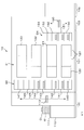
- FIG. 2 is a plan view schematically showing an outline of the configuration of each substrate processing system 10.
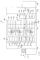
- 3 and 4 are a front view and a rear view schematically showing an outline of the internal configuration of each substrate processing system 10.
- each substrate processing system 10 includes a cassette station 100 into which a cassette C containing a plurality of wafers W is carried in and out, and a plurality of processing devices that perform predetermined processing on the wafer W. It has a station 101 and.
- Each substrate processing system 10 has a configuration in which a cassette station 100, a processing station 101, and an interface station 103 that transfers a wafer W between an exposure device 102 adjacent to the processing station 101 are integrally connected. ing.
- the cassette station 100 is provided with a cassette mounting stand 110.
- the cassette mounting table 110 is provided with a plurality of cassette mounting plates 111 on which the cassette C is mounted when the cassette C is carried in and out of the substrate processing system 10.
- the cassette station 100 is provided with a wafer transfer device 113 that is movable on a transfer path 112 extending in the X direction.
- the wafer transfer device 113 is also movable in the vertical direction and around the vertical axis ( ⁇ direction), and is a transfer device for the cassette C on each cassette mounting plate 111 and the third block G3 of the processing station 101 described later. Wafer W can be conveyed between them.
- the processing station 101 is provided with a plurality of, for example, four blocks equipped with various devices, that is, first blocks G1 to fourth blocks G4.
- a first block G1 is provided on the front side of the processing station 101 (negative direction in the X direction in FIG. 2), and on the back side of the processing station 101 (positive direction in the X direction in FIG. 2, upper side in the drawing).
- a third block G3 is provided on the cassette station 100 side of the processing station 101 (negative direction side in the Y direction in FIG. 2), and the interface station 103 side of the processing station 101 (positive direction side in the Y direction in FIG. 2).
- a liquid processing apparatus which is a substrate processing apparatus for processing the wafer W using the processing liquid is arranged.
- a liquid treatment device for example, a development processing device 120, a lower layer film forming device 121, an intermediate layer film forming device 122, and a resist coating device 123 are below the first block G1 as liquid treatment devices, as shown in FIG. They are arranged in this order.
- the developing processing apparatus 120 develops the wafer W. Specifically, the developing processing apparatus 120 supplies a developing solution onto the resist film of the wafer W to form a resist pattern.
- the underlayer film forming apparatus 121 forms an underlayer film which is a base film of the resist film of the wafer W. Specifically, the underlayer film forming apparatus 121 coats the underlayer film material, which is a material for forming the underlayer film, on the wafer W to form the underlayer film.
- the underlayer film is, for example, an SOC (spin-on carbon) film.
- the intermediate layer film forming apparatus 122 forms the intermediate layer film on the lower layer film of the wafer W at a position below the resist film. Specifically, the intermediate layer film forming apparatus 122 coats the intermediate layer film material, which is a material for forming the intermediate layer film, on the lower layer film of the wafer W to form the intermediate layer film.
- the intermediate layer film is, for example, an SOG (spin-on-glass) film.
- the resist coating device 123 applies a resist solution to the wafer W to form a resist film. Specifically, the resist coating apparatus 123 applies a resist solution on the intermediate layer film of the wafer W to form a resist film.
- the developing processing device 120, the lower layer film forming device 121, the intermediate layer film forming device 122, and the resist coating device 123 are arranged side by side in the horizontal direction.
- the number and arrangement of the developing processing apparatus 120, the lower layer film forming apparatus 121, the intermediate layer film forming apparatus 122, and the resist coating apparatus 123 can be arbitrarily selected.
- a predetermined processing liquid is applied onto the wafer W by a spin coating method.
- the processing liquid is discharged onto the wafer W from the coating nozzle, and the wafer W is rotated to diffuse the processing liquid on the surface of the wafer W.
- a heat treatment apparatus 130 which is a substrate processing apparatus for performing heat treatment such as heating and cooling of the wafer W by using a hot plate or a cooling plate on which the wafer W is placed, is provided side by side in the vertical direction and the horizontal direction. Has been done.
- the number and arrangement of these heat treatment devices 130 can be arbitrarily selected. Further, known devices can be used for the heat treatment device 130.
- a plurality of delivery devices 140, 141, 142, 143, 144 are provided in order from the bottom, and examination imaging devices 145, 146, 147 are provided in order from the bottom.
- a plurality of delivery devices 150, 151, 152 are provided in order from the bottom, and inspection imaging devices 153, 154 are provided on the plurality of delivery devices 150, 151, 152 in order from the bottom.
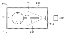
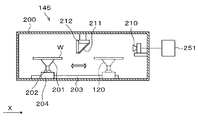
- the inspection imaging device 145 has a casing 200 as shown in FIGS. 5 and 6.
- a mounting table 201 on which the wafer W is mounted is provided in the casing 200.
- the mounting table 201 can be freely rotated and stopped by a rotation driving unit 202 such as a motor.
- a guide rail 203 extending from one end side (negative direction side in the X direction in FIG. 6) to the other end side (positive direction side in the X direction in FIG. 6) in the casing 200 is provided on the bottom surface of the casing 200. ..
- the mounting table 201 and the rotary drive unit 202 are provided on the guide rail 203, and can be moved along the guide rail 203 by the drive device 204.
- An imaging unit 210 is provided on the side surface of the casing 200 on the other end side (the positive direction side in the X direction in FIG. 6).
- a wide-angle CCD camera is used for the image pickup unit 210.
- a half mirror 211 is provided near the center of the upper part of the casing 200.
- the half mirror 211 is provided at a position facing the image pickup unit 210 in a state in which the mirror surface is inclined 45 degrees upward from the state in which the mirror surface faces vertically downward toward the image pickup section 210.
- a lighting device 212 is provided above the half mirror 211.
- the half mirror 211 and the lighting device 212 are fixed to the upper surface inside the casing 200.
- the illumination from the illumination device 212 passes through the half mirror 211 and is illuminated downward. Therefore, the light reflected by the object below the lighting device 212 is further reflected by the half mirror 211 and taken into the image pickup unit 210. That is, the imaging unit 210 can image an object in the irradiation region by the lighting device 212. Then, the imaging result by the imaging unit 210 is input to the imaging control device 251 described later.
- the configuration of the inspection imaging device 146, 147, 153, and 154 is the same as the configuration of the inspection imaging device 145 described above.
- a wafer transfer region D is formed in a region surrounded by the first block G1 to the fourth block G4.
- a plurality of wafer transfer devices 160 having transfer arms 160a that can move in the Y direction, the X direction, the ⁇ direction, and the vertical direction are arranged.
- the wafer transfer device 160 moves in the wafer transfer area D and transfers the wafer W to desired devices in the surrounding first block G1, second block G2, third block G3, and fourth block G4. it can.
- the wafer transfer region D is provided with a shuttle transfer device 170 that linearly conveys the wafer W between the third block G3 and the fourth block G4.
- the shuttle transport device 170 is linearly movable in the Y direction of FIG. 4, for example.
- the shuttle transfer device 170 moves in the Y direction while supporting the wafer W, and can transfer the wafer W between the transfer device 142 of the third block G3 and the transfer device 152 of the fourth block G4.
- a wafer transfer device 180 is provided next to the third block G3 on the positive direction side in the X direction.
- the wafer transfer device 180 has, for example, a transfer arm 180a that can move in the X direction, the ⁇ direction, and the vertical direction.
- the wafer transfer device 180 can move up and down while supporting the wafer W to transfer the wafer W to each transfer device in the third block G3.
- the interface station 103 is provided with a wafer transfer device 190 and a transfer device 191.
- the wafer transfer device 190 has, for example, a transfer arm 190a that can move in the Y direction, the ⁇ direction, and the vertical direction.
- the wafer transfer device 190 can, for example, support the wafer W on the transfer arm 190a and transfer the wafer W between each transfer device, the transfer device 191 and the exposure device 102 in the fourth block G4.
- the substrate processing system 10 is provided with a transport / process control device 250 and an image pickup control device 251 as a substrate inspection device.
- the transport / process control device 250 (hereinafter, may be referred to as "main control device 250") is, for example, a computer equipped with a CPU, a memory, or the like, and has a program storage unit (not shown).
- a program for controlling the operation of the drive system of the above-mentioned various processing devices and transfer devices to perform various processing on the wafer W is stored.
- the program may be recorded on a storage medium readable by a computer and may be installed on the main control device 250 from the storage medium. Part or all of the program may be realized by dedicated hardware (circuit board).
- the image pickup control device 251 is a computer equipped with, for example, a CPU, a memory, and the like, and has a program storage unit (not shown).
- a program that controls the operation of the imaging unit and the drive system of each inspection imaging device and controls the processing related to the substrate inspection is stored.
- the above program may be recorded on a storage medium readable by a computer and may be installed on the image pickup control device 251 from the storage medium. Part or all of the program may be realized by dedicated hardware (circuit board).
- the substrate inspection system 1 has an overall control device 20.
- the overall control device 20 is, for example, a computer equipped with a CPU, a memory, or the like, and has a program storage unit (not shown).
- a program for creating an image estimation model described later is stored in this program storage unit.
- the program may be recorded on a computer-readable storage medium and may be installed on the overall control device 20 from the storage medium. Part or all of the program may be realized by dedicated hardware (circuit board).
- FIG. 7 is a block diagram schematically showing an outline of the configurations of the image pickup control device 251 and the overall control device 20 regarding the substrate inspection.
- the overall control device 20 has a storage unit 301 and a model creation unit 302.
- the storage unit 301 stores various information.
- the captured image of the wafer W acquired from the result of imaging the wafer W by the imaging unit 210 of the inspection imaging device in each substrate processing system 10 is stored.
- the captured image and the estimated image described later are assumed to be grayscale images. However, these images may be images of at least one of the R component, the G component, and the B component.
- Each captured image is associated with identification information of the imaged wafer W, identification information of the processing device used for processing the imaged wafer W, and the like.
- the model creation unit 302 describes the image captured before the desired processing by the substrate processing system 10 and the image captured after the desired processing for each of the plurality of wafers W (hereinafter, “imaging before and after processing by the substrate processing system 10”).
- An image estimation model is created by machine learning using an "image set").
- the image estimation model is a model that estimates the captured image of the inspection target wafer W after the desired processing by the substrate processing system 10 from the captured image of the inspection target wafer W before the desired processing by the substrate processing system 10.
- the image estimation model is a model that generates an estimated image of the inspection target wafer W after the processing from the captured image of the inspection target wafer W before the processing.
- the machine learning used to create the image estimation model is, for example, machine learning by a conditional GAN (Generative Adversarial Networks), and more specifically, pix2pix.
- the image estimation model is, for example, a generation network (Generator) that converts an arbitrary input image to generate a fake image in a conditional hostile generation network or pix2pix.
- a discriminator is used as the neural network in addition to the above generation network.
- the identification network a real image corresponding to the arbitrary image or a fake image generated by the generation network based on the arbitrary image is input together with the arbitrary image, and the image input together with the arbitrary image is a real image. It identifies whether it is a fake image or a fake image. Then, in machine learning by the conditional hostile generation network and fix2pix, the identification method is learned so that the above identification can be performed accurately for the identification network, and for the generation network, the fake image is a real image in the identification network. The image conversion method is learned so that it can be recognized.
- the model creation unit 302 uses an image set before and after processing in the substrate processing system 10 as an image set of the arbitrary image input to the identification network and a real image corresponding to the arbitrary image.
- the image estimation model created by the model creation unit 302 is sent to the image pickup control device 251 of the substrate processing system 10.
- the image pickup control device 251 includes a storage unit 311, an image capture image acquisition unit 312, an estimation image acquisition unit 313, and a determination unit 314.
- the storage unit 311 stores various information.
- the storage unit 311 stores, for example, an image estimation model created by the model creation unit 302 of the overall control device 20.
- the captured image acquisition unit 312 acquires an captured image of the wafer W based on the imaging result of the wafer W by the imaging unit 210 of the inspection imaging devices 145, 146, 147, 153, and 154. Specifically, the captured image acquisition unit 312 performs necessary image processing on the image captured by the imaging unit 210, thereby showing the state of the entire surface of the wafer W as the captured image of the wafer W. Generate an image.
- the captured image acquisition unit 312 acquires captured images of the wafer W to be inspected before the desired processing and after the desired processing in the substrate processing system 10, and also performs inspection before the desired processing and after the desired processing.
- the captured image of the target wafer W which is used to create the image estimation model, is acquired.
- the estimated image acquisition unit 313 is based on the captured image of the wafer W to be inspected before the desired processing by the substrate processing system 10 acquired by the captured image acquisition unit 312 and the image estimation model stored in the storage unit 311. , An estimated image of the wafer W to be inspected after the desired processing is generated and acquired.
- the overall control device 20 uses the image estimation model to generate an estimated image of the wafer W to be inspected after the desired processing, and the estimated image acquisition unit 313 acquires the generated estimated image. May be good.
- the determination unit 314 determines the presence or absence of defects in the inspection target wafer W based on the captured image of the inspection target wafer W after the desired processing by the substrate processing system 10 acquired by the captured image acquisition unit 312.
- the determination unit 314 includes the captured image of the inspection target wafer W after the desired processing acquired by the captured image acquisition unit 312 and the inspection target wafer after the desired processing acquired by the estimation image acquisition unit 313. Based on the estimated image of W, the presence or absence of defects in the wafer W to be inspected is determined.
- the determination unit 314 compares the captured image of the inspection target wafer W after the desired processing with the estimated image of the inspection target wafer W after the desired processing, and based on the comparison result, the said The presence or absence of defects in the wafer W to be inspected is determined. More specifically, the determination unit 314 determines the inspection target wafer based on the difference between the captured image of the inspection target wafer W after the desired processing and the estimated image of the inspection target wafer W after the desired processing. Determine if there is a defect in W.
- the wafer W is imaged at three or more timings, but the defect inspection based on the image captured by the wafer W is performed only by the defect inspection based on the image captured by the wafer W after the resist pattern is formed. And. Further, prior to the following processing on the wafer W and inspection of the wafer W, it is assumed that the machine learning of the image estimation model for the wafer W after forming the resist pattern, which is used for the defect inspection, has been completed.
- the image estimation model is based on, for example, an image of the wafer W after forming the resist film of the wafer W (that is, before forming the resist pattern) in each substrate processing system 10 and the wafer W after forming the resist pattern. Will be created.
- the cassette C containing the plurality of wafers W is carried into the cassette station 100. Then, under the control of the main control device 250, the wafer W in the cassette C is conveyed to the inspection imaging device 145 of the third block G3. Then, under the control of the image pickup control device 251, an image is taken by the image pickup unit 210 of the wafer W in the initial state before forming various films such as the lower layer film, and the image pickup image acquisition unit 312 performs the image pickup in the initial state. The captured image of the wafer W of the above is acquired.
- the wafer W is conveyed to the lower layer film forming device 121 of the first block G1 to form the lower layer film on the wafer W. Subsequently, the wafer W is conveyed to the heat treatment apparatus 130 for the lower layer film of the second block G2, and the lower layer film is heat-treated. After that, the wafer W is conveyed to the inspection imaging device 153. Then, under the control of the image pickup control device 251 the image pickup unit 210 takes an image of the wafer W after the lower layer film is formed, and the captured image of the wafer W after the lower layer film is formed is acquired.
- the wafer W is conveyed to the intermediate layer film forming device 122 of the first block G1 to form an intermediate layer film on the lower layer film of the wafer W.
- the wafer W is transferred to the heat treatment apparatus 130 for the intermediate layer of the second block G2, and the intermediate layer film is heat-treated.
- the wafer W is conveyed to the inspection imaging device 146.
- the image pickup unit 210 takes an image of the wafer W after the intermediate layer film is formed, and the image pickup image acquisition unit 312 acquires an image of the wafer W after the intermediate layer film is formed. Will be done.
- the wafer W is conveyed to the resist coating device 123 of the first block G1 to form a resist film on the intermediate layer film of the wafer W.
- the wafer W is transferred to the heat treatment apparatus 130 for PAB processing of the second block G2, and PAB processing is performed.
- the wafer W is conveyed to the inspection imaging device 153.
- the image pickup control device 251 the image pickup unit 210 takes an image of the wafer W after the resist film is formed, and the image pickup image acquisition unit 312 acquires an image of the wafer W after the resist film is formed. ..
- the wafer W is conveyed to the exposure device 102 under the control of the main control device 250 and exposed to a desired pattern. Subsequently, the wafer W is conveyed to the heat treatment apparatus 130 for PEB processing of the second block G2, and PEB processing is performed. Next, the wafer is conveyed to the developing processing apparatus 120 of the first block G1, the developing processing is performed, and a resist pattern is formed on the wafer W. After that, the wafer W is transferred to the inspection imaging device 147. Then, under the control of the image pickup control device 251 the image pickup unit captures the image of the wafer W after the resist pattern is formed, and the image pickup image acquisition unit 312 acquires the image image of the wafer W after the resist pattern formation.
- the presence or absence of defects in the wafer after forming the resist pattern is determined based on the captured image of the wafer W after forming the resist pattern acquired by the captured image acquisition unit 312. Specifically, after forming the resist pattern, based on an image of the wafer W after forming the resist film (that is, before forming the resist pattern) and an image estimation model for the wafer W after forming the resist pattern created in advance. An estimated image of the wafer W is generated by the estimated image acquisition unit 313. Then, the determination unit 314 determines the presence or absence of defects in the wafer W after the resist pattern formation (that is, the wafer W to be inspected) based on the captured image of the wafer W after the resist pattern formation and the estimated image.
- the captured image and the estimated image are compared, and the portion where the pixel values of both images differ by a threshold value or more is the portion where the defect exists. It is determined that the other parts are free of defects.
- the creation of the image estimation model for the wafer W after forming the resist pattern is not completed, the presence or absence of defects in the wafer W is determined in the same manner as in the conventional case. If the estimation model has not been created, the image captured after the resist film is formed and the image captured after the resist pattern is formed for the wafer W are input to the model creation unit 302 of the overall control device 20. Machine learning of the above model is advanced.
- the wafer W is returned to the cassette C under the control of the main control device 250, and the processing for the wafer W is completed. Then, the above-mentioned processing is also performed on the other wafer W.
- images created by machine learning are used for each of the plurality of wafers W before the desired processing in the substrate processing system 10 and the captured images after the desired processing.
- An estimation model is used.
- This image estimation model is a model that creates an estimated image of the wafer W after the desired processing from the captured image of the wafer W before the desired processing in the substrate processing system 10.
- an estimated image of the inspection target wafer W after the desired processing is generated and acquired based on the image estimation model and the captured image of the inspection target wafer W before the desired processing. Then, the presence or absence of defects in the inspection target wafer W is determined based on the captured image actually acquired for the inspection target wafer W after the desired processing and the above estimation image.
- the presence or absence of defects in the inspection target wafer is determined based on a reference image that is suitable for each inspection target wafer W and is a reference for defect inspection. Therefore, the defect detection accuracy can be improved.
- the reference image used as the reference for defect inspection is an estimated image generated based on the above image estimation model, the captured image and the estimated image, that is, the reference for the wafer W to be inspected after the desired processing. The unevenness is almost the same as the image. Therefore, since the possibility that unevenness is detected as a defect is low, the defect detection accuracy can be improved.
- the captured image and the estimated image are compared with each other for the wafer W to be inspected after the desired processing as described above, there is no possibility that unevenness is erroneously detected as a defect.
- the above-mentioned threshold value can be reduced. Therefore, it is possible to detect a defect that cannot be detected when the threshold value is large.
- FIG. 8 is a conceptual diagram for explaining an example of a conventional defect inspection
- FIG. 9 is a conceptual diagram for explaining an example of a defect inspection according to the present embodiment.
- the horizontal axis shows the coordinates of each part along a certain direction on the wafer with respect to the direction
- the vertical axis shows the value such as the pixel value of each part.
- FIG. 8A shows an example of the relationship between the captured image Ip of the inspection target wafer W and the average image Ia described later
- FIG. 8B shows the captured image Ip of the inspection target wafer W and the average described later. The difference from the image Ia is shown
- FIG. 8C shows an example of the defect determination value Vc described later in the conventional defect inspection.
- FIG. 9 (A) shows an example of the relationship between the captured image Ip of the wafer W to be inspected and the corresponding estimated image Ie
- FIG. 9 (B) shows the defect determination value V described later according to the present embodiment. An example is shown.
- captured images are acquired for a plurality of wafers W after a desired process, and an average image Ia and a standard deviation image Is are acquired from the captured images of the plurality of wafers W.
- the average image Ia is an image in which the average value of each pixel in the captured images of the plurality of wafers W is the pixel value of each pixel.
- the captured image Ip of the wafer W to be inspected and FIG. 8A are shown. There is such a relationship.
- the standard deviation image Is is an image in which the standard deviation of each pixel in the captured images of the plurality of wafers W is used as the pixel value of each pixel.
- the difference between the captured image Ip of the wafer W to be inspected and the average image Ia is calculated.
- the portion having a significant value in the above difference includes not only the defective portion but also the portion caused by unevenness. Therefore, the standard deviation image Is is applied as a variation filter for removing unevenness, and a defect determination value Vc is generated. Specifically, in the pixels in which the absolute value of the pixel value of the difference exceeds the absolute value of the pixel value of the standard deviation image Is, the pixel value of the standard deviation image Is is subtracted from the pixel value of the difference for each pixel. , The defect determination value Vc as shown in FIG. 8C is generated.
- the portion exceeding the threshold value Tc is determined to be a defect.
- the standard deviation image Is as a variation filter for removing unevenness is not unique to each wafer W and does not accurately represent unevenness. Therefore, as shown in FIG. 8C, the portion having a significant value in the defect determination value includes not only the portion caused by the defects K1, K2, K3 but also the portion caused by the unevenness U.
- the threshold value Tc with respect to the defect determination value is set large. That is, the detection sensitivity is set low. Therefore, only the defects K1 and K2 showing a large value in the defect determination value Vc may be detected, and the defect K3 to be detected showing a small value in the defect determination value Vc may not be detected.
- the captured image Ip of the wafer W to be inspected after the desired processing and the estimated image Ie serving as the reference image for the defect inspection have a relationship as shown in FIG. 9A, for example.
- the difference between the captured image Ip of the wafer W to be inspected after the desired processing and the estimated image Ie in each pixel is defined as the defect determination value V, and in this defect determination value V, the portion exceeding the threshold value T is defined as the defect. It is judged.
- the estimated image Ie used for the defect determination of the present embodiment is created based on the image estimation model created by machine learning as described above, is unique to each wafer W, and is an inspection target before desired processing. The state of the wafer W is reflected.
- the unevenness is substantially the same in the captured image Ip and the estimated image Ie of the wafer W to be inspected after the desired processing, and as shown in FIG. 9B, a portion showing a significant value in the defect determination value V.
- a portion showing a significant value in the defect determination value V Does not include a portion caused by unevenness, but includes only a portion caused by defects K1, K2, and K3. Therefore, even if the threshold value T with respect to the defect determination value V is reduced, the uneven portion is not detected as a defect. Therefore, the threshold value T is set small, that is, the detection sensitivity is set high, and the defect determination value is set. Defect K3, which shows a small value in V, can also be accurately detected.
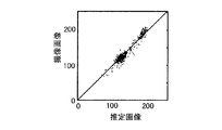
- the present inventors actually created an image estimation model by machine learning using an image of the wafer W after forming the resist film and an image of the wafer W after forming the resist pattern. Then, an estimated image after forming the resist pattern of the inspection target wafer W is generated from the captured image of the inspection target wafer W after forming the resist film and the created image estimation model, and the resist pattern of the inspection target wafer W is formed. It was compared with the actual captured image later. The results are shown in FIGS. 10 and 11. 10 and 11 are diagrams showing the relationship between the pixel value of the actual captured image and the pixel value of the estimated image for each part of the image. FIG. 10 shows the whole wafer, and FIG. 11 shows only the central portion of the wafer. As shown in FIGS.
- FIGS. 10 and 11 in each part of the image, the pixel value of the actual captured image and the pixel value of the estimated image show close values.
- the pixel value of the actual captured image and the pixel value of the estimated image are substantially the same.
- FIGS. 10 and 11 are for the pixel value of the R component, it has been confirmed by the present inventors that the G component and the B component also show the same tendency as the R component.
- an image estimation model for the wafer W to be inspected after the resist pattern is formed is created based on the image of the wafer W after the resist film is formed and the image of the wafer W after the resist pattern is formed. It was. Instead, an image estimation model for the wafer W to be inspected after the resist pattern is formed based on the image of the wafer W in the initial state before the lower layer film is formed and the image of the wafer W after the resist pattern is formed. May be created. Then, the estimated image of the inspection target wafer W after forming the resist pattern is estimated based on the image estimation model and the captured image of the inspection target wafer W in the initial state, and after the resist pattern is formed based on this estimated image. The defect inspection of the wafer W to be inspected may be performed.
- the present inventors actually created an image estimation model by machine learning using the captured image of the wafer W in the initial state and the captured image of the wafer W after forming the resist pattern. Then, an estimated image of the inspection target wafer W after forming the resist pattern is generated from the captured image of the inspection target wafer W in the initial state and the created image estimation model, and after the resistance pattern of the inspection target wafer W is formed. It was compared with the actual captured image of. The results are shown in FIGS. 12 and 13. 12 and 13 are diagrams showing the relationship between the pixel value of the actual captured image and the pixel value of the estimated image for each part of the image. FIG. 12 shows the whole wafer, and FIG. 13 shows only the central portion of the wafer. As shown in FIGS.
- FIGS. 12 and 13 are for the pixel value of the R component, it has been confirmed by the present inventors that the G component and the B component also show the same tendency as the R component.
- the wafer to be inspected after forming the resist pattern based on the image of the wafer W after forming the lower layer film, the image of the wafer W after forming the intermediate layer film, and the image of the wafer W after forming the resist pattern, the wafer to be inspected after forming the resist pattern.
- An image estimation model for W may be created. Then, the estimated image of the inspection target wafer W after the resist pattern formation is estimated based on the image estimation model, the captured image of the inspection target wafer W after the lower layer film formation, and the wafer after the intermediate layer film formation. Based on this estimated image, a defect inspection of the wafer W to be inspected after forming the resist pattern may be performed.
- the following captured images may be used to generate the model. That is, not only the captured image of the wafer W immediately before the processing of the m item (in other words, after the processing of the (m-1) item), but also the processing of the (m-2) item immediately before the processing of the (m-1) item.
- the captured image of the wafer W of the latter may be used.
- the image estimation model for example, a common image is created among the substrate processing systems by using the captured images acquired by the plurality of substrate processing systems 10 of the substrate inspection system 1. Instead, the image estimation model for a certain substrate processing system 10 may be created using only the captured images acquired by the substrate processing system. As a result, an image estimation model that reflects the characteristics of the substrate processing system 10 can be created.
- the captured image of the wafer W determined to have a defect by the defect inspection may be removed from the captured image of the wafer W used for creating the image estimation model. This makes it possible to create a more accurate image estimation model.
- the substrate inspection method according to the present embodiment is a single film forming. It can also be applied when processing is performed. Further, the substrate inspection method according to the present embodiment can also be applied to a case where a process other than the film forming process (for example, an etching process) is performed.
- FIG. 14 is a block diagram showing an outline of another example of the overall control device, and shows a configuration related to substrate inspection.
- the overall control device 20a of FIG. 14 has a storage unit 301 and a model creation unit 302, similarly to the overall control device 20 of FIG. Then, the overall control device 20a further selects a plurality of captured image sets used for creating an image estimation model by the model creating unit 302, that is, a plurality of captured image sets for model creation from a large number of captured image sets. It has a part 400.
- the captured image set is an image set composed of a combination of a captured image before processing by the substrate processing system 10 and a captured image after processing for a certain wafer W.
- the selection unit 400 determines the degree of abnormality for each captured image set, and selects the captured image set for model creation based on the degree of abnormality.
- the degree of abnormality is the in-plane tendency of the pixel value in the image (hereinafter, may be referred to as “IN image”) of the wafer W before the desired processing in the substrate processing system 10 and the processing in the substrate processing system 10. It is determined by using the correlation distribution with the in-plane tendency of the pixel value in the image (hereinafter sometimes referred to as “OUT image”) of the wafer W later.
- the selection unit 400 has, for example, a candidate acquisition unit 401, a coefficient calculation unit 402, a distance calculation unit 403, and an extraction unit 404.
- the candidate acquisition unit 401 acquires a plurality of captured image sets from the storage unit 301 as candidates for the captured image set for model creation.
- the coefficient calculation unit 402 uses a Zernike polynomial to determine the plane distribution of the pixel values in the captured image for each captured image of the wafer W included in the captured image set acquired by the candidate acquisition unit 401. Each value is decomposed into in-plane tendency components, and the Zernike coefficient of each in-plane tendency component is calculated.
- the captured image of the wafer W is generally composed of three primary colors of RGB (Red, Green, Blue). Therefore, the in-plane tendency component Zi of the pixel value can be obtained for each of the primary colors R, G, and B, but there is no difference in the image processing method among R, G, and B. Therefore, in the following, it is assumed that all the primary colors R, G, and B are processed in parallel even if not specified.
- RGB Red, Green, Blue
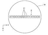
- the coefficient calculation unit 402 first digitizes the color of the captured image for each captured image of the wafer W included in the captured image set acquired by the candidate acquisition unit 401 as a pixel value, for example, in pixel units over the entire surface of the wafer W. .. As a result, the plane distribution of pixel values in the wafer plane is obtained. Then, the coefficient calculation unit 402 decomposes the plane distribution of the pixel values in the wafer plane into the in-plane tendency component Zi (i is an integer of 1 or more) of a plurality of pixel values. As shown in FIG. 15, the in-plane tendency component Zi of the plurality of pixel values is represented by decomposing the plane distribution Z of the pixel values in the wafer plane into a plurality of components using a Zernike polynomial.
- Zernike polynomials are complex functions mainly used in the field of optics and have two degrees (n, m). It is also a function on the unit circle with a radius of 1, and has polar coordinate arguments (r, ⁇ ).
- This Zernike polynomial is used in the field of optics, for example, to analyze the aberration component of a lens, and by decomposing the wave surface aberration using the Zernike polynomial, each independent wave surface, for example, a mountain shape or a saddle shape, is formed.
- the underlying aberration component can be known.
- FIG. 16 shows the plane distribution Z of the pixel value of each pixel P in the plane of the wafer W, and the numerical value described inside each pixel P indicates the pixel value of the pixel P.
- FIGS. 16 and 17 only one row of pixels P along the X-axis direction is described in FIGS. 16 and 17.
- the pixel values of each pixel P are set in the height direction on the wafer W surface (FIG. 17).
- the planar distribution of the pixel values of each pixel P can be grasped as a curve having a predetermined shape drawn in three dimensions. Then, by expressing the pixel values of all the pixels P in the wafer W plane in the height direction on the wafer W plane in the same manner, the distribution of the pixel values in the wafer W plane can be grasped as a three-dimensional circular wave plane. Can be done.
- the Zernike polynomial can be applied by capturing it as a three-dimensional wave plane in this way, and the plane distribution Z of the pixel values in the wafer plane can be calculated by using the Zernike polynomial, for example, the inclination component in the vertical and horizontal directions in the wafer plane, convex or convex. It can be decomposed into an in-plane tendency component Zi of a plurality of pixel values such as a curved component that curves in a concave shape. The magnitude of each of the in-plane tendency components Zi of the pixel value can be expressed by the Zernike coefficient.
- the Zernike coefficient representing the in-plane tendency component Zi of the pixel value can be specifically expressed using the arguments (r, ⁇ ) and the order (n, m) of polar coordinates.
- the Zernike coefficients from the 1st to 9th terms are shown below as an example.
- the Zernike coefficient Z1 which is the Zernike coefficient of one item means the average value of the pixel values in the wafer surface
- the second Zernike coefficient Z2 is the inclination component of the pixel values in the wafer surface in the left-right direction
- the third Zernike coefficient Z3 is the inclination component of the pixel value in the wafer surface in the anteroposterior direction (the direction orthogonal to the inclination direction of the Zernike coefficient Z2)
- the fourth Zernike coefficient is uniform in the circumferential direction with the center of the wafer as the origin and in the radial direction. Means the curvature component of the pixel value that gradually increases.
- the coefficient calculation unit 402 calculates the values of the in-plane tendency component Zi of the pixel values obtained by decomposing the plane distribution Z of the pixel values in the wafer surface as described above. Specifically, since the magnitude of the in-plane tendency component Zi of the pixel value is represented by the Zernike coefficient as described above, the value of each in-plane tendency component Zi of the pixel value is calculated by obtaining the value of each Zernike coefficient. To do.
- the distance calculation unit 403 is a set of captured images acquired by the candidate acquisition unit 401 based on the correlation distribution between the Zernike coefficient in the IN image and the Zernike coefficient in the OUT image for each term (for each degree) in the Zernike polynomial. Calculate the Mahalanobis distance for each.
- the distance calculation unit 403 sets the space to which the correlation distribution belongs (that is, the Zernike coefficient in the IN image and the Zernike coefficient in the OUT image) for each term in the Zernike polynomial for each of the captured image sets acquired by the candidate acquisition unit 401.
- the Mahalanobis distance MD (see FIG. 19 described later) between the point indicating the captured image set and the correlation distribution in the distribution space (consisting of the distribution space) is calculated.
- the extraction unit 404 determines the degree of abnormality for each of the captured image sets acquired by the candidate acquisition unit 401 based on the Mahalanobis distance calculated by the distance calculation unit 403. Then, the extraction unit 404 extracts and selects the captured image set for model creation from the captured image set acquired by the candidate acquisition unit 401 based on the determined abnormality degree.
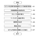
- FIG. 18 is a diagram showing a flow of selection processing of a captured image set for model creation by the selection unit 400.
- FIG. 19 is a diagram for explaining the Mahalanobis distance.
- FIG. 20 is a diagram conceptually showing a method of calculating the degree of abnormality.
- the candidate acquisition unit 401 of the selection unit 400 acquires a plurality of captured image sets from the storage unit 301 as candidates for the captured image set for model creation (step S1). At that time, the candidate acquisition unit 401 excludes the captured image set for the wafer W determined to be “defective” by the defect inspection from the candidates for the captured image set for model creation. The candidate acquisition unit 401 was determined to be "defective” regardless of whether it was determined to be "defective” in the defect inspection based on the IN image or "defective" in the defect inspection based on the OUT image. The captured image set for the wafer W is excluded.
- the coefficient calculation unit 402 performs enhancement processing on each of the captured images (that is, IN image and OUT image) included in the captured image set acquired by the candidate acquisition unit 401 (step S2).
- the enhancement process is, for example, a process for enhancing the contrast in each captured image.
- the coefficient calculation unit 402 decomposes the plane distribution of the pixel values in the captured image of the highlighted wafer W into in-plane tendency components Zi of a plurality of pixel values using the Zernike polynomial.
- the Zernike coefficient of each in-plane tendency component is calculated (step S3).
- the coefficient calculation unit 402 uses the Zernike polynomial to determine the planar distribution of the pixel values in the emphasized wafer W for each captured image (that is, for each of the emphasized IN image and OUT image). And calculate the coefficient of each term in the approximation formula, that is, the Zernike coefficient.
- the coefficient calculation unit 402 calculates, for example, the Zernike coefficients from the first term to the 16th term in the Zernike polynomial. The calculation of the Zernike coefficient as described above by the coefficient calculation unit 402 is performed for each of RGB, for example.
- the distance calculation unit 403 calculates the Mahalanobis distance MD for each term in the Zernike polynomial for each of the captured image sets acquired by the candidate acquisition unit 401 (step S4).
- the Mahalanobis distance MD for each term in the Zernike polynomial calculated here is a point P indicating a set of captured images to be calculated in the distribution space K of the Zernike coefficient between the IN image and the OUT image.
- the Mahalanobis distance represents a measure between the sample points and the distribution.
- the Mahalanobis distance MD from the vector y to the distribution with mean ⁇ and covariance ⁇ can be calculated by the following formula.
- the distance calculation unit 403 calculates the Mahalanobis distance MD of each of the captured image sets acquired by the candidate acquisition unit 401 for each of the first to 16th terms in the Zernike polynomial. Further, the Mahalanobis distance for each term in the Zernike polynomial is calculated for each of RGB, for example. Further, the Mahalanobis distance calculated for each term in the Zernike polynomial may be normalized by dividing by the average value in the corresponding term.
- the extraction unit 404 determines the degree of abnormality Ab of each captured image set based on the Mahalanobis distance calculated for each term in the Zernike polynomial by the distance calculation unit 403 for each captured image set (step S5). For example, the extraction unit 404 determines the degree of abnormality Ab by adding the Mahalanobis distance MD calculated for each term in the Zernike polynomial by the distance calculation unit 403 for each of the captured image sets.
- the extraction unit 404 calculates the Mahalanobis distance MD for R, which is calculated by the distance calculation unit 403 for each of the first to 16th terms in the Zernike polynomial, for example. Add all the captured image sets. Then, the extraction unit 404, the result of the sum (i.e. the sum of the Mahalanobis distance MD), determines the degree of abnormality Ab r for R of the captured images set. Similarly, the extraction unit 404 adds up all the Mahalanobis distance MDs for G calculated for each of the first to 16th terms in the Zernike polynomial by the distance calculation unit 403 for each captured image set, for example. The degree of anomaly Ab g for G of each captured image set is determined.
- the extraction unit 404 adds all the Mahalanobis distance MDs for B calculated for each of the first to 16th terms in the Zernike polynomial by the distance calculation unit 403 for each captured image set, and each is added.
- the degree of abnormality Ab b for B of the captured image set is determined. That is, the extraction unit 404 adds all the Mahalanobis distance MDs calculated for each of the first to 16th terms in the Zernike polynomial and for each of the RGB colors for each of the RGB colors and for each captured image set.
- weighting may be performed for each term in the Zernike polynomial. Further, for each of the captured image sets, when the distance calculation unit 403 adds the Mahalanobis distances calculated for each term in the Zernike polynomial and for each color of RGB, weighting may be performed for each color.
- the extraction unit 404 sets the abnormality determination threshold Th for the abnormality degree Ab determined by the extraction unit 404 (step S6).
- the extraction unit 404 calculates the threshold value Th c based on the following formula.
- Ab Ave indicates the average value of the abnormality degree Ab determined by the extraction unit 404
- Ab Std indicates the standard deviation of the abnormality degree Ab determined by the extraction unit 404
- c is, for example, 1 to 3. It is an integer.
- Th c Ab Ave + c ⁇ Ab Std
- the extraction unit 404 sets the calculated threshold value Th c as the threshold value Th for abnormality determination.
- a lower limit value of the threshold value Th for abnormality determination may be provided, and when the threshold value Th c calculated based on the above equation is lower than the lower limit value, the lower limit value may be set as the threshold value Th for abnormality determination.
- the calculation of the threshold value Th c based on the above equation and the setting of the threshold value Th of the abnormality determination are performed for each of RGB.
- the threshold values Th for abnormality determination for each of R, G, and B are set to Th r , Th g , and Th b .
- the extraction unit 404 extracts and selects the captured image set for model creation based on the abnormality degree Ab of each of the captured image sets determined by the extraction unit 404 and the threshold value Th set by the extraction unit 404. (Step S7). Specifically, the extraction unit 404 captures an image set for model creation in which the abnormality degree Ab, which is the sum of the Mahalanobis distance MDs, does not exceed the abnormality determination threshold Th among the captured image sets acquired by the candidate acquisition unit 401. Extract as an image set. More specifically, the extraction unit 404 extracts an image set that satisfies all of the following conditions (x1) to (x3) for model creation.
- the quality of the image estimation model can be ensured by automatically selecting the optimum image set for learning the image estimation model from a large number of captured image sets, and further, this image estimation model can be used.
- the accuracy of defect detection used can be improved.
- the extraction method of the captured image set for model creation based on the Mahalanobis distance by the extraction unit 404 is not limited to the above example. For example, it may be as follows.
- the extraction unit 404 sets the Mahalanobis distance MD calculated by the distance calculation unit 403 to the abnormality degree Ab for each term in the Zernike polynomial for each captured image set. More specifically, the extraction unit 404 calculates, for example, the Mahalanobis distance MD for R calculated by the distance calculation unit 403 for each of the first to 16th terms in the Zernike polynomial for each R of each captured image set. The degree of abnormality is set to Ab r1 to Ab r16 . Similarly, the extraction unit 404 calculates, for example, the Mahalanobis distance MD for G calculated by the distance calculation unit 403 for each of the first to 16th terms in the Zernike polynomial for each G of each captured image set.
- the degree of abnormality is set to Ab g1 to Ab g16 .
- the extraction unit 404 calculates, for example, the Mahalanobis distance MD for B calculated by the distance calculation unit 403 for each of the first to 16th terms in the Zernike polynomial, and abnormalities for B in each captured image set. The degree is set to Ab b1 to Ab b16 .
- the extraction unit 404 sets a threshold value Th for abnormality determination for each term in the Zernike polynomial with respect to the abnormality degree Ab set by the extraction unit 404.
- the extraction unit 404 calculates the threshold value Th c for each of the first to 16th terms in the Zernike polynomial.
- the same formula as described above can be used.
- the extraction unit 404 sets the calculated threshold value Th c as the threshold value Th for abnormality determination for each of the first to 16th terms in the Zernike polynomial.
- the lower limit value of the threshold value Th of the abnormality determination may be provided as described above.
- the calculation of the threshold value Th c and the setting of the threshold value Th of the abnormality determination are performed for each of RGB.
- the threshold values Th for abnormality determination for R related to each of the first to 16th terms in the Zernike polynomial are set to Th r1 to Th r16
- the threshold value Th for abnormality determination for G is set to Th g1 to Th g1 to. It is set to Th g16
- the threshold value Th of the abnormality determination for B is set to Th b1 to Th b16 .
- the extraction unit 404 uses the captured image set acquired by the candidate acquisition unit 401 for creating a model of the captured image set having no term (order) in the Zernike polynomial whose abnormality degree Ab exceeds the abnormality determination threshold Th. Extract as a set of captured images. More specifically, when n is an integer of 1 to 16, the extraction unit 404 extracts an image set that satisfies all of the following conditions (y1) to (y3) for model creation.
- (Y1) For the nth term in the Zernike polynomial, the degree of anomaly Ab rn ⁇ threshold Th rn .
- Y2 For the nth term in the Zernike polynomial, the degree of anomaly Ab gn ⁇ threshold Th gn .
- the degree of anomaly Ab bn ⁇ threshold Th bn For the nth term in the Zernike polynomial, the degree of anomaly Ab bn ⁇ threshold Th bn .
- the Mahalanobis distance was calculated for all colors and all terms in all Zernike polynomials, but the Mahalanobis distance calculation etc. was omitted for some colors and some terms. You may try to do it. Colors that omit the calculation of the Mahalanobis distance and the information in the above items are stored in the storage unit 301 in advance.
- FIG. 21 is a diagram illustrating another example of a method for calculating the Mahalanobis distance.
- the correlation distribution C between the Zernike coefficient in the IN image and the Zernike coefficient in the OUT image is not integrated, and an appropriate Mahalanobis distance cannot be calculated, so that the captured image for model creation is not possible. You may not be able to select the set properly.
- the correlation distribution C may be divided into a plurality of sub-correlation distributions. For example, the correlation distribution C may be divided into two sub-correlation distributions C1 and C2 as shown in FIG. Then, when the distance calculation unit 403 calculates the Mahalanobis distance of the captured image set, the Mahalanobis distance between the sub-correlation distribution to which the captured image set belongs and the point indicating the captured image set may be calculated. Good.
- the unit of division of the correlation distribution C into the sub-correlation distribution is, for example, each lot of the wafer W, each device, each transfer route, that is, each passage module.
- a board inspection device that inspects a board.
- An image estimation model created by machine learning using an image captured before processing by a substrate processing device and an image captured after processing for each of a plurality of substrates, and an image captured by the substrate to be inspected before processing by the substrate processing device.
- an image estimation model created by machine learning using captured images of a plurality of substrates before and after processing is used to generate a reference image as a reference for defect inspection, and the presence or absence of defects on the substrate to be inspected. Is determined. Since the reference image used as the reference for defect inspection is an estimated image generated based on the image estimation model, the unevenness of the captured image and the reference image of the processed substrate to be inspected becomes substantially the same. Therefore, since the possibility that unevenness is detected as a defect is low, the defect detection accuracy can be improved.
- the determination unit determines the presence or absence of defects in the inspection target substrate based on the difference between the captured image of the inspection target substrate and the estimated image after processing by the substrate processing device. Or the substrate inspection apparatus according to (2).
- the determination unit determines the presence or absence of defects in the inspection target substrate based on an image of the inspection target substrate after processing by the substrate processing apparatus and an image of a substrate center portion in the estimated image.
- the substrate inspection apparatus according to any one of (1) to (3). According to (4) above, defect inspection can be performed more accurately.
- the image estimation model is a generation network that generates a fake image by converting an arbitrary input image in a conditional hostile generation network.
- a real image corresponding to the arbitrary image or the fake image generated based on the arbitrary image is input together with the arbitrary image in the conditional hostile generation network, and the input image together with the arbitrary image is
- the identification method is machine-learned so that the identification is performed accurately.
- a board inspection system that inspects boards.
- a board processing device that processes the board and Equipped with a control device, The control device
- a creation unit that creates an image estimation model by machine learning using an image captured before processing by the substrate processing device and an image captured after processing for each of a plurality of substrates.
- a generation unit that generates an estimated image of the inspection target substrate after processing by the substrate processing apparatus based on an image of the inspection target substrate before processing by the substrate processing apparatus and the image estimation model.
- a substrate inspection system including a determination unit for determining the presence or absence of defects in the inspection target substrate based on an image captured by the inspection target substrate after processing by the substrate processing apparatus and the estimated image.
- the image estimation model is a generation network that generates a fake image by converting an arbitrary input image in a conditional hostile generation network.
- a real image corresponding to the arbitrary image or the fake image generated based on the arbitrary image is input together with the arbitrary image in the conditional hostile generation network, and the input image together with the arbitrary image is
- the identification method is machine-learned so that the identification is performed accurately.
- a selection unit for selecting an image set for model creation which is an image set including a combination of an image of the substrate before the processing and an image of the substrate after the processing, is further provided.
- the selection unit determines the degree of anomaly determined by using the correlation distribution between the in-plane tendency of the pixel value in the captured image of the substrate before the processing and the in-plane tendency of the pixel value in the captured image of the substrate after the processing.
- the selection unit is As candidates for the captured image set for model creation, a candidate acquisition unit for acquiring a plurality of the captured image sets, and a candidate acquisition unit.
- the plane distribution of the pixel values in the captured image is decomposed into in-plane tendency components of a plurality of pixel values using a Zernike polynomial, and each A coefficient calculation unit that calculates the Zernike coefficient of the in-plane tendency component, and
- the Mahalanobis distance of each of the captured image sets is based on the correlation distribution between the Zernike coefficient in the captured image of the substrate before the processing and the Zernike coefficient in the captured image of the substrate after the processing.
- the substrate inspection system which comprises an extraction unit for extracting an image set.
- the extraction unit is For each of the captured image sets, the Mahalanobis distance calculated by the distance calculation unit for each term in the Zernike polynomial is added to determine the degree of abnormality.
- the captured image set acquired by the acquisition unit, wherein the abnormality degree obtained by adding the Mahalanobis distances does not exceed the threshold value is extracted as the captured image set for creating the model, according to the above (9). Board inspection system.
- the degree of abnormality is a Mahalanobis distance calculated by the distance calculation unit for each term in the Zernike polynomial.
- the extraction unit extracts a captured image set having no term in the Zernike polynomial whose degree of abnormality exceeds the threshold value from the captured image set as the captured image set for creating the model. The substrate inspection system described.
- a substrate inspection method for inspecting a substrate The process of acquiring an image of the substrate to be inspected before processing by the substrate processing device, and The process of acquiring an image of the substrate to be inspected after processing by the substrate processing apparatus, and An image estimation model created by machine learning using an image captured before processing by the substrate processing device and an image captured after processing for each of a plurality of substrates, and an image captured by the substrate to be inspected before processing by the substrate processing device.
- a step of acquiring an estimated image of the inspection target substrate after processing by the substrate processing apparatus and A substrate inspection method comprising a step of determining the presence or absence of defects in the inspection target substrate based on an image of the inspection target substrate after processing by the substrate processing apparatus and the estimated image.
- the image estimation model is a generation network that generates a fake image by converting an arbitrary input image in a conditional hostile generation network.
- a real image corresponding to the arbitrary image or the fake image generated based on the arbitrary image is input together with the arbitrary image in the conditional hostile generation network, and the input image together with the arbitrary image is
- the identification method is machine-learned so that the identification is performed accurately.
- An estimation model of an captured image of a substrate used when inspecting a substrate is The computer functions so as to estimate the captured image of the inspection target substrate after processing by the substrate processing device from the image of the inspection target substrate before processing by the substrate processing device.
- the conditional hostile generation network it is a generation network that converts an arbitrary input image to generate a fake image.
- a real image corresponding to the arbitrary image or the fake image generated based on the arbitrary image is input together with the arbitrary image, and is input together with the arbitrary image.
- the identification method For the identification network that discriminates whether the image is the real image or the fake image, the identification method is learned so that the identification is performed accurately, and the generation network is the fake in the identification network.
- An estimation model in which an image conversion method is learned so that an image is recognized as a real image.
- Substrate inspection system 20 Overall control device 120 Development processing device 121 Underlayer film forming device 122 Intermediate layer film forming device 123 Resist coating device 130 Heat treatment device 251 Imaging control device 302 Model creation unit 313 Estimated image acquisition unit 314 Judgment unit Ie Estimated image Ip Captured images K1, K2, K3 Defect W wafer
Landscapes
- Engineering & Computer Science (AREA)
- Physics & Mathematics (AREA)
- General Physics & Mathematics (AREA)
- Manufacturing & Machinery (AREA)
- Biochemistry (AREA)
- Immunology (AREA)
- Health & Medical Sciences (AREA)
- Life Sciences & Earth Sciences (AREA)
- Chemical & Material Sciences (AREA)
- Analytical Chemistry (AREA)
- Pathology (AREA)
- General Health & Medical Sciences (AREA)
- Computer Hardware Design (AREA)
- Power Engineering (AREA)
- Microelectronics & Electronic Packaging (AREA)
- Quality & Reliability (AREA)
- Computer Vision & Pattern Recognition (AREA)
- Theoretical Computer Science (AREA)
- Condensed Matter Physics & Semiconductors (AREA)
- Investigating Materials By The Use Of Optical Means Adapted For Particular Applications (AREA)
- Testing Or Measuring Of Semiconductors Or The Like (AREA)
- Image Analysis (AREA)
Abstract
Description
図示するように、基板検査システム1は、複数の基板処理システム10と、全体制御装置20とを有している。なお、基板検査システム1が有する基板処理システム10の台数は1つであってもよい。 FIG. 1 is a diagram schematically showing an outline of the configuration of a substrate inspection system according to the present embodiment.
As shown in the figure, the
図5及び図6はそれぞれ、検査用撮像装置145の構成の概略を示す縦断面図及び横断面図である。
検査用撮像装置145は、図5及び図6に示すように、ケーシング200を有している。ケーシング200内には、ウェハWが載置される載置台201が設けられている。この載置台201は、モータ等の回転駆動部202によって、回転、停止が自在である。ケーシング200の底面には、ケーシング200内の一端側(図6中のX方向負方向側)から他端側(図6中のX方向正方向側)まで延伸するガイドレール203が設けられている。載置台201と回転駆動部202は、ガイドレール203上に設けられ、駆動装置204によってガイドレール203に沿って移動できる。 Here, the configuration of the
5 and 6 are a vertical sectional view and a horizontal sectional view showing an outline of the configuration of the
The
図2に示すように第1のブロックG1~第4のブロックG4に囲まれた領域には、ウェハ搬送領域Dが形成されている。ウェハ搬送領域Dには、例えばY方向、X方向、θ方向及び上下方向に移動自在な搬送アーム160aを有する、ウェハ搬送装置160が複数配置されている。ウェハ搬送装置160は、ウェハ搬送領域D内を移動し、周囲の第1のブロックG1、第2のブロックG2、第3のブロックG3及び第4のブロックG4内の所望の装置にウェハWを搬送できる。 Returning to the description of each
As shown in FIG. 2, a wafer transfer region D is formed in a region surrounded by the first block G1 to the fourth block G4. In the wafer transfer region D, for example, a plurality of
基板検査システム1は、前述のように、全体制御装置20を有する。
全体制御装置20は、例えばCPUやメモリ等を備えたコンピュータであり、プログラム格納部(図示せず)を有している。このプログラム格納部には、後述の画像推定モデルを作成するためのプログラムが格納されている。なお、上記プログラムは、コンピュータで読み取り可能な記憶媒体に記録されていたものであって、当該記憶媒体から全体制御装置20にインストールされたものであってもよい。プログラムの一部または全ては専用ハードウェア(回路基板)で実現してもよい。 Returning to the description of the
As described above, the
The
全体制御装置20は、図示するように、記憶部301と、モデル作成部302とを有する。 FIG. 7 is a block diagram schematically showing an outline of the configurations of the image
As shown in the figure, the
また、画像推定モデルは、例えば、条件付き敵対的生成ネットワークやpix2pixにおいて、入力された任意の画像を変換して偽物画像を生成する生成ネットワーク(Generator)である。 The machine learning used to create the image estimation model is, for example, machine learning by a conditional GAN (Generative Adversarial Networks), and more specifically, pix2pix.
Further, the image estimation model is, for example, a generation network (Generator) that converts an arbitrary input image to generate a fake image in a conditional hostile generation network or pix2pix.
そして、条件付き敵対的生成ネットワークによる機械学習やpix2pixでは、識別ネットワークについて、上記識別が正確に行われるよう識別方法が学習され、また、生成ネットワークについて、識別ネットワークにおいて偽物画像が本物画像であると認識されるよう画像の変換方法が学習される。 In the conditional hostile generation network and pix2pix, a discriminator is used as the neural network in addition to the above generation network. In the identification network, a real image corresponding to the arbitrary image or a fake image generated by the generation network based on the arbitrary image is input together with the arbitrary image, and the image input together with the arbitrary image is a real image. It identifies whether it is a fake image or a fake image.
Then, in machine learning by the conditional hostile generation network and fix2pix, the identification method is learned so that the above identification can be performed accurately for the identification network, and for the generation network, the fake image is a real image in the identification network. The image conversion method is learned so that it can be recognized.
モデル作成部302で作成された画像推定モデルは、基板処理システム10の撮像制御装置251に送られる。 The
The image estimation model created by the
この撮像画像取得部312は、基板処理システム10での所望の処理前及び上記所望の処理後の検査対象ウェハWの撮像画像を取得し、また、上記所望の処理前及び所望の処理後の検査対象ウェハWの撮像画像であって画像推定モデルの作成に用いられる撮像画像を取得する。 The captured
The captured
続いて、ウェハWが、第2のブロックG2の下層膜用の熱処理装置130に搬送され、下層膜の加熱処理が行われる。
その後、ウェハWが、検査用撮像装置153へ搬送される。そして、撮像制御装置251の制御の下、撮像部210による下層膜形成後のウェハWの撮像が行われ、当該下層膜形成後のウェハWの撮像画像が取得される。 Next, under the control of the
Subsequently, the wafer W is conveyed to the
After that, the wafer W is conveyed to the
続いて、ウェハWが、第2のブロックG2の中間層用の熱処理装置130に搬送され、中間層膜の加熱処理が行われる。
その後、ウェハWが、検査用撮像装置146へ搬送される。そして、撮像制御装置251の制御の下、撮像部210による中間層膜形成後のウェハWの撮像が行われ、撮像画像取得部312により、当該中間層膜形成後のウェハWの撮像画像が取得される。 Next, under the control of the
Subsequently, the wafer W is transferred to the
After that, the wafer W is conveyed to the
続いて、ウェハWが、第2のブロックG2のPAB処理用の熱処理装置130に搬送され、PAB処理が行われる。
その後、ウェハWが、検査用撮像装置153へ搬送される。そして、撮像制御装置251の制御の下、撮像部210によるレジスト膜形成後のウェハWの撮像が行われ、撮像画像取得部312により、当該レジスト膜形成後のウェハWの撮像画像が取得される。 Next, under the control of the
Subsequently, the wafer W is transferred to the
After that, the wafer W is conveyed to the
続いて、ウェハWが、第2のブロックG2のPEB処理用の熱処理装置130に搬送され、PEB処理が行われる。
次に、ウェハが、第1のブロックG1の現像処理装置120に搬送され、現像処理が行われ、当該ウェハW上にレジストパターンが形成される。
その後、ウェハWが検査用撮像装置147に搬送される。そして、撮像制御装置251の制御の下、撮像部によるレジストパターン形成後のウェハWの撮像が行われ、撮像画像取得部312により、当該レジストパターン形成後のウェハWの撮像画像が取得される。 Next, the wafer W is conveyed to the
Subsequently, the wafer W is conveyed to the
Next, the wafer is conveyed to the developing
After that, the wafer W is transferred to the
この欠陥の有無の判定では、例えば、レジストパターン形成後のウェハWについて、撮像画像と推定画像とが比較され、両画像の画素値に閾値以上の差がある部分は、欠陥が存在する部分と判定され、それ以外の部分は、欠陥がない部分と判定される。 Next, the presence or absence of defects in the wafer after forming the resist pattern is determined based on the captured image of the wafer W after forming the resist pattern acquired by the captured
In the determination of the presence or absence of this defect, for example, in the wafer W after forming the resist pattern, the captured image and the estimated image are compared, and the portion where the pixel values of both images differ by a threshold value or more is the portion where the defect exists. It is determined that the other parts are free of defects.
図8は、従来の欠陥検査の一例を説明するための概念図であり、図9は、本実施形態にかかる欠陥検査の一例を説明するための概念図である。図8及び図9において、横軸は、ウェハ上のある方向に沿った各部分の当該方向に関する座標を示し、縦軸は、上記各部分の画素値等の値を示す。図8(A)には、検査対象ウェハWの撮像画像Ipと後述の平均画像Iaの関係の一例が示され、図8(B)には、検査対象ウェハWの撮像画像Ipと後述の平均画像Iaとの差分が示され、図8(C)には、従来の欠陥検査にかかる後述の欠陥判定値Vcの一例が示されている。図9(A)には、検査対象ウェハWの撮像画像Ipと対応する推定画像Ieの関係の一例が示され、図9(B)には、本実施形態にかかる後述の欠陥判定値Vの一例が示されている。 The effect of the defect inspection according to the present embodiment will be described more specifically with reference to FIGS. 8 and 9.
FIG. 8 is a conceptual diagram for explaining an example of a conventional defect inspection, and FIG. 9 is a conceptual diagram for explaining an example of a defect inspection according to the present embodiment. In FIGS. 8 and 9, the horizontal axis shows the coordinates of each part along a certain direction on the wafer with respect to the direction, and the vertical axis shows the value such as the pixel value of each part. FIG. 8A shows an example of the relationship between the captured image Ip of the inspection target wafer W and the average image Ia described later, and FIG. 8B shows the captured image Ip of the inspection target wafer W and the average described later. The difference from the image Ia is shown, and FIG. 8C shows an example of the defect determination value Vc described later in the conventional defect inspection. FIG. 9 (A) shows an example of the relationship between the captured image Ip of the wafer W to be inspected and the corresponding estimated image Ie, and FIG. 9 (B) shows the defect determination value V described later according to the present embodiment. An example is shown.
しかし、ムラを除去するためのバリエーションフィルタとしての上記標準偏差画像Isは、ウェハW毎に固有のものではなくムラを正確に現したものではない。そのため、図8(C)に示すように、欠陥判定値において有意な値を有する部分に、欠陥K1、K2、K3に起因する部分だけでなく、ムラUに起因する部分も含まれる。このムラUの部分が欠陥として検出されるのを防ぐため、従来の欠陥検査方法では、欠陥判定値に対する上記閾値Tcが大きく設定されている。つまり、検出感度が低く設定されている。そのため、欠陥判定値Vcにおいて大きな値を示す欠陥K1、K2だけ検出され、欠陥判定値Vcにおいて小さな値を示す、検出すべき欠陥K3を検出することができないことがある。 Then, in the conventional defect inspection, the difference between the captured image Ip of the wafer W to be inspected and the average image Ia is calculated. As shown in FIG. 8B, the portion having a significant value in the above difference includes not only the defective portion but also the portion caused by unevenness. Therefore, the standard deviation image Is is applied as a variation filter for removing unevenness, and a defect determination value Vc is generated. Specifically, in the pixels in which the absolute value of the pixel value of the difference exceeds the absolute value of the pixel value of the standard deviation image Is, the pixel value of the standard deviation image Is is subtracted from the pixel value of the difference for each pixel. , The defect determination value Vc as shown in FIG. 8C is generated. In the conventional defect inspection, in this defect determination value, the portion exceeding the threshold value Tc is determined to be a defect.
However, the standard deviation image Is as a variation filter for removing unevenness is not unique to each wafer W and does not accurately represent unevenness. Therefore, as shown in FIG. 8C, the portion having a significant value in the defect determination value includes not only the portion caused by the defects K1, K2, K3 but also the portion caused by the unevenness U. In order to prevent the uneven U portion from being detected as a defect, in the conventional defect inspection method, the threshold value Tc with respect to the defect determination value is set large. That is, the detection sensitivity is set low. Therefore, only the defects K1 and K2 showing a large value in the defect determination value Vc may be detected, and the defect K3 to be detected showing a small value in the defect determination value Vc may not be detected.
図10及び図11に示すように、画像の各部分において、上記実際の撮像画像の画素値と、上記推定画像の画素値は、近い値を示していた。特に、図11に示すように、ウェハ中央部では、上記実際の撮像画像の画素値と上記推定画像の画素値とは略同一であった。
なお、図10及び図11は、R成分の画素値についてのものであるが、G成分、B成分においても、R成分と同様の傾向を示すことが、本発明者らによって確認されている。 The present inventors actually created an image estimation model by machine learning using an image of the wafer W after forming the resist film and an image of the wafer W after forming the resist pattern. Then, an estimated image after forming the resist pattern of the inspection target wafer W is generated from the captured image of the inspection target wafer W after forming the resist film and the created image estimation model, and the resist pattern of the inspection target wafer W is formed. It was compared with the actual captured image later. The results are shown in FIGS. 10 and 11. 10 and 11 are diagrams showing the relationship between the pixel value of the actual captured image and the pixel value of the estimated image for each part of the image. FIG. 10 shows the whole wafer, and FIG. 11 shows only the central portion of the wafer.
As shown in FIGS. 10 and 11, in each part of the image, the pixel value of the actual captured image and the pixel value of the estimated image show close values. In particular, as shown in FIG. 11, in the central portion of the wafer, the pixel value of the actual captured image and the pixel value of the estimated image are substantially the same.
Although FIGS. 10 and 11 are for the pixel value of the R component, it has been confirmed by the present inventors that the G component and the B component also show the same tendency as the R component.
図12及び図13に示すように、画像の各部分において、上記実際の撮像画像の画素値と、上記推定画像の画素値は、近い値を示していた。特に、図13に示すように、ウェハ中央部では、上記実際の撮像画像の画素値と上記推定画像の画素値とは略同一であった。
なお、図12及び図13は、R成分の画素値についてのものであるが、G成分、B成分においても、R成分と同様の傾向を示すことが、本発明者らによって確認されている。 The present inventors actually created an image estimation model by machine learning using the captured image of the wafer W in the initial state and the captured image of the wafer W after forming the resist pattern. Then, an estimated image of the inspection target wafer W after forming the resist pattern is generated from the captured image of the inspection target wafer W in the initial state and the created image estimation model, and after the resistance pattern of the inspection target wafer W is formed. It was compared with the actual captured image of. The results are shown in FIGS. 12 and 13. 12 and 13 are diagrams showing the relationship between the pixel value of the actual captured image and the pixel value of the estimated image for each part of the image. FIG. 12 shows the whole wafer, and FIG. 13 shows only the central portion of the wafer.
As shown in FIGS. 12 and 13, in each part of the image, the pixel value of the actual captured image and the pixel value of the estimated image showed close values. In particular, as shown in FIG. 13, in the central portion of the wafer, the pixel value of the actual captured image and the pixel value of the estimated image are substantially the same.
Although FIGS. 12 and 13 are for the pixel value of the R component, it has been confirmed by the present inventors that the G component and the B component also show the same tendency as the R component.
これに代えて、ある基板処理システム10についての画像推定モデルは、当該基板処理システムで取得された撮像画像のみを用いて作成してもよい。これにより、当該基板処理システム10の特性を反映した画像推定モデルを作成することができる。 As for the image estimation model, for example, a common image is created among the substrate processing systems by using the captured images acquired by the plurality of
Instead, the image estimation model for a certain
図14の全体制御装置20aは、図7の全体制御装置20と同様、記憶部301とモデル作成部302とを有する。そして、全体制御装置20aはさらに、多数の撮像画像セットの中から、モデル作成部302での画像推定モデルの作成に用いられる撮像画像セット、すなわち、モデル作成用の撮像画像セットを複数選択する選択部400を有する。なお、撮像画像セットとは、あるウェハWについての基板処理システム10による処理前の撮像画像と処理後の撮像画像との組み合わせからなる画像セットである。 FIG. 14 is a block diagram showing an outline of another example of the overall control device, and shows a configuration related to substrate inspection.
The
Z1,n=0,m=0 (1)
Z2,n=1,m=1 (r・cosθ)
Z3,n=0,m=-1 (r・sinθ)
Z4,n=2,m=0 (2r2-1)
Z5,n=2,m=2 (r2・cos2θ)
Z6,n=2,m=-2 (r2・sin2θ)
Z7,n=3,m=1 ((3r3-2r)・cosθ)
Z8,n=3,m=-1 ((3r3-2r)・sinθ)
Z9,n=4,m=0 (6r4-6r2+1)
・
・
・ The Zernike coefficient representing the in-plane tendency component Zi of the pixel value can be specifically expressed using the arguments (r, θ) and the order (n, m) of polar coordinates. The Zernike coefficients from the 1st to 9th terms are shown below as an example.
Z1, n = 0, m = 0 (1)
Z2, n = 1, m = 1 (r · cos θ)
Z3, n = 0, m = -1 (r · sinθ)
Z4, n = 2, m = 0 (2r 2 -1)
Z5, n = 2, m = 2 (r 2 · cos2θ)
Z6, n = 2, m = -2 (r 2 · sin2θ)
Z7, n = 3, m = 1 ((3r 3 -2r) · cosθ)
Z8, n = 3, m = -1 ((3r 3 -2r) · sinθ)
Z9, n = 4, m = 0 (6r 4 -6r 2 +1)
・
・
・
係数算出部402では、ウェハ面内の画素値の平面分布Zを上述のように分解して得られた、画素値の面内傾向成分Ziそれぞれの値を算出する。具体的には、画素値の面内傾向成分Ziの大きさは上述のとおりゼルニケ係数により表されるので、各ゼルニケ係数の値を求めることで画素値の面内傾向成分Ziそれぞれの値を算出する。 Returning to the description of FIG.
The
なお、マハラノビス距離は、標本点と分布の間の尺度を表すものである。ベクトルyから平均μ及び共分散Σを持つ分布までのマハラノビス距離MDは以下の式で算出することができる。 Next, the
The Mahalanobis distance represents a measure between the sample points and the distribution. The Mahalanobis distance MD from the vector y to the distribution with mean μ and covariance Σ can be calculated by the following formula.

また、ゼルニケ多項式における各項毎のマハラノビス距離の算出は、例えばRGBそれぞれについて行われる。
さらに、ゼルニケ多項式における各項毎に算出したマハラノビス距離に対して、該当する項における平均値で除算する規格化処理を行ってもよい。 The
Further, the Mahalanobis distance for each term in the Zernike polynomial is calculated for each of RGB, for example.
Further, the Mahalanobis distance calculated for each term in the Zernike polynomial may be normalized by dividing by the average value in the corresponding term.
Thc=AbAve+c×AbStd
抽出部404は、算出した閾値Thcを、異常判定の閾値Thとして設定する。なお、算出し設定した閾値Thcが小さすぎると、後述のステップS7のモデル作成用の画像撮像画像セット抽出工程において、必要以上の撮像画像セットがモデル作成用の撮像画像セットから除外される場合もある。したがって、異常判定の閾値Thの下限値を設けておき、上記式に基づいて算出された閾値Thcが上記下限値を下回る場合に、上記下限値を異常判定の閾値Thとしてもよい。これら、上記式に基づく閾値Thcの算出及び異常判定の閾値Thの設定はRGBそれぞれについて行われる。なお、以下では、R、G、Bそれぞれについての異常判定の閾値ThをThr、Thg、Thbとする。 Next, the
Th c = Ab Ave + c × Ab Std
The
(x1)Rについての異常度Abr≧Rについての異常判定の閾値Thr
(x2)Gについての異常度Abg≧Gについての異常判定の閾値Thg
(x3)Bについての異常度Abb≧Bについての異常判定の閾値Thb Then, the
(X1) threshold of abnormality determination of the degree of abnormality Ab r ≧ R for R Th r
(X2) Abnormality of G Ab g ≧ G Abnormality determination threshold Th g
(X3) Abnormality degree Ab b ≥ B threshold value for abnormality determination Th b
(y1)ゼルニケ多項式における第n項について異常度Abrn≧閾値Thrnである。
(y2)ゼルニケ多項式における第n項について異常度Abgn≧閾値Thgnである。
(y3)ゼルニケ多項式における第n項について異常度Abbn≧閾値Thbnである。 Then, the
(Y1) For the nth term in the Zernike polynomial, the degree of anomaly Ab rn ≧ threshold Th rn .
(Y2) For the nth term in the Zernike polynomial, the degree of anomaly Ab gn ≧ threshold Th gn .
(Y3) For the nth term in the Zernike polynomial, the degree of anomaly Ab bn ≧ threshold Th bn .
図21に示すように、IN画像でのゼルニケ係数とOUT画像でのゼルニケ係数との相関分布Cが一纏まりとならず、適切なマハラノビス距離を算出することができなくなり、モデル作成用の撮像画像セットを適切に選択できない場合がある。この場合は、相関分布Cを複数のサブ相関分布に分割してもよい。例えば、相関分布Cを図21のように2つのサブ相関分布C1、C2に分割してもよい。そして、距離算出部403が撮像画像セットのマハラノビス距離を算出する際は、当該撮像画像セットが属するサブ相関分布と、当該撮像画像セットを示す点との間のマハラノビス距離を算出するようにしてもよい。 FIG. 21 is a diagram illustrating another example of a method for calculating the Mahalanobis distance.
As shown in FIG. 21, the correlation distribution C between the Zernike coefficient in the IN image and the Zernike coefficient in the OUT image is not integrated, and an appropriate Mahalanobis distance cannot be calculated, so that the captured image for model creation is not possible. You may not be able to select the set properly. In this case, the correlation distribution C may be divided into a plurality of sub-correlation distributions. For example, the correlation distribution C may be divided into two sub-correlation distributions C1 and C2 as shown in FIG. Then, when the
(1)基板を検査する基板検査装置であって、
複数の基板それぞれについての基板処理装置による処理前の撮像画像及び処理後の撮像画像を用いて機械学習により作成された画像推定モデルと、前記基板処理装置による処理前の検査対象基板の撮像画像と、に基づく、前記基板処理装置による処理後の前記検査対象基板の推定画像を取得する取得部と、
前記基板処理装置による処理後の前記検査対象基板の撮像画像と前記推定画像とに基づいて、当該検査対象基板の欠陥の有無を判定する判定部と、を有する、基板検査装置。
前記(1)では、複数の基板についての処理前後の撮像画像を用いて機械学習により作成された画像推定モデルが使用され欠陥検査の基準となる基準画像が生成され、検査対象基板の欠陥の有無の判定が行われる。欠陥検査の基準となる基準画像が、上記画像推定モデルに基づいて生成された推定画像であるため、処理後の検査対象基板についての、撮像画像と基準画像とでムラが略同じになる。したがって、ムラが欠陥として検出される可能性が低いため、欠陥検出精度を向上させることができる。 The following configurations also belong to the technical scope of the present disclosure.
(1) A board inspection device that inspects a board.
An image estimation model created by machine learning using an image captured before processing by a substrate processing device and an image captured after processing for each of a plurality of substrates, and an image captured by the substrate to be inspected before processing by the substrate processing device. To acquire an estimated image of the inspection target substrate after processing by the substrate processing apparatus based on
A substrate inspection apparatus having a determination unit for determining the presence or absence of defects in the inspection target substrate based on an image captured by the inspection target substrate after processing by the substrate processing apparatus and the estimated image.
In (1) above, an image estimation model created by machine learning using captured images of a plurality of substrates before and after processing is used to generate a reference image as a reference for defect inspection, and the presence or absence of defects on the substrate to be inspected. Is determined. Since the reference image used as the reference for defect inspection is an estimated image generated based on the image estimation model, the unevenness of the captured image and the reference image of the processed substrate to be inspected becomes substantially the same. Therefore, since the possibility that unevenness is detected as a defect is low, the defect detection accuracy can be improved.
前記(4)によれば、より正確に欠陥検査を行うことができる。 (4) The determination unit determines the presence or absence of defects in the inspection target substrate based on an image of the inspection target substrate after processing by the substrate processing apparatus and an image of a substrate center portion in the estimated image. The substrate inspection apparatus according to any one of (1) to (3).
According to (4) above, defect inspection can be performed more accurately.
前記条件付き敵対的生成ネットワークにおける、任意の画像と共に当該任意の画像に対応する本物画像または当該任意の画像に基づいて生成された前記偽物画像が入力され、当該任意の画像と共に入力された画像が前記本物画像であるか前記偽物画像であるかの識別を行う識別ネットワークについて、前記識別が正確に行われるよう識別方法が機械学習され、
前記生成ネットワークについて、前記識別ネットワークにおいて前記偽物画像が前記本物画像であると認識されるよう画像の変換方法が機械学習される、前記(2)~(5)のいずれか1に記載の基板検査装置。 (5) The image estimation model is a generation network that generates a fake image by converting an arbitrary input image in a conditional hostile generation network.
A real image corresponding to the arbitrary image or the fake image generated based on the arbitrary image is input together with the arbitrary image in the conditional hostile generation network, and the input image together with the arbitrary image is For the identification network that discriminates whether the image is a real image or a fake image, the identification method is machine-learned so that the identification is performed accurately.
The substrate inspection according to any one of (2) to (5) above, wherein the image conversion method is machine-learned for the generated network so that the fake image is recognized as the real image in the identification network. apparatus.
基板を処理する基板処理装置と、
制御装置と、を備え、
前記制御装置は、
複数の基板それぞれについての前記基板処理装置による処理前の撮像画像及び処理後の撮像画像を用い、機械学習により画像推定モデルを作成する作成部と、
前記基板処理装置による処理前の検査対象基板の撮像画像と、前記画像推定モデルとに基づいて、前記基板処理装置による処理後の前記検査対象基板の推定画像を生成する生成部と、
前記基板処理装置による処理後の前記検査対象基板の撮像画像と前記推定画像とに基づいて、当該検査対象基板の欠陥の有無を判定する判定部と、を有する、基板検査システム。 (6) A board inspection system that inspects boards.
A board processing device that processes the board and
Equipped with a control device,
The control device
A creation unit that creates an image estimation model by machine learning using an image captured before processing by the substrate processing device and an image captured after processing for each of a plurality of substrates.
A generation unit that generates an estimated image of the inspection target substrate after processing by the substrate processing apparatus based on an image of the inspection target substrate before processing by the substrate processing apparatus and the image estimation model.
A substrate inspection system including a determination unit for determining the presence or absence of defects in the inspection target substrate based on an image captured by the inspection target substrate after processing by the substrate processing apparatus and the estimated image.
前記条件付き敵対的生成ネットワークにおける、任意の画像と共に当該任意の画像に対応する本物画像または当該任意の画像に基づいて生成された前記偽物画像が入力され、当該任意の画像と共に入力された画像が前記本物画像であるか前記偽物画像であるかの識別を行う識別ネットワークについて、前記識別が正確に行われるよう識別方法が機械学習され、
前記生成ネットワークについて、前記識別ネットワークにおいて前記偽物画像が前記本物画像であると認識されるよう画像の変換方法が機械学習される、前記(6)に記載の基板検査システム。 (7) The image estimation model is a generation network that generates a fake image by converting an arbitrary input image in a conditional hostile generation network.
A real image corresponding to the arbitrary image or the fake image generated based on the arbitrary image is input together with the arbitrary image in the conditional hostile generation network, and the input image together with the arbitrary image is For the identification network that discriminates whether the image is a real image or a fake image, the identification method is machine-learned so that the identification is performed accurately.
The substrate inspection system according to (6) above, wherein an image conversion method is machine-learned for the generation network so that the fake image is recognized as the real image in the identification network.
前記選択部は、前記処理前の基板の撮像画像における画素値の面内傾向と、前記処理後の基板の撮像画像における画素値の面内傾向との相関分布を用いて決定される異常度に基づいて、モデル作成用の前記撮像画像セットを選択する、前記(6)または(7)に記載の基板検査システム。 (8) A selection unit for selecting an image set for model creation, which is an image set including a combination of an image of the substrate before the processing and an image of the substrate after the processing, is further provided.
The selection unit determines the degree of anomaly determined by using the correlation distribution between the in-plane tendency of the pixel value in the captured image of the substrate before the processing and the in-plane tendency of the pixel value in the captured image of the substrate after the processing. The substrate inspection system according to (6) or (7) above, wherein the captured image set for model creation is selected based on the above.
モデル作成用の前記撮像画像セットの候補として、複数の前記撮像画像セットを取得する候補取得部と、
取得された前記撮像画像セットに含まれる前記基板の撮像画像毎に、当該撮像画像内の画素値の平面分布を、ゼルニケ多項式を用いて複数の画素値の面内傾向成分にそれぞれ分解し、各面内傾向成分のゼルニケ係数をそれぞれ算出する係数算出部と、
ゼルニケ多項式における各項毎に、前記処理前の前記基板の撮像画像におけるゼルニケ係数と、前記処理後の前記基板の撮像画像におけるゼルニケ係数との相関分布に基づいて、前記撮像画像セットそれぞれのマハラノビス距離を算出する距離算出部と、
前記撮像画像セットそれぞれについて、前記マハラノビス距離に基づいて、異常度を決定すると共に、前記異常度に基づいて、前記候補取得部が取得した前記撮像画像セットの中から、前記モデル作成用の前記撮像画像セットを抽出する抽出部と、を有する、前記(8)に記載の基板検査システム。 (9) The selection unit is
As candidates for the captured image set for model creation, a candidate acquisition unit for acquiring a plurality of the captured image sets, and a candidate acquisition unit.
For each captured image of the substrate included in the acquired captured image set, the plane distribution of the pixel values in the captured image is decomposed into in-plane tendency components of a plurality of pixel values using a Zernike polynomial, and each A coefficient calculation unit that calculates the Zernike coefficient of the in-plane tendency component, and
For each term in the Zernike polynomial, the Mahalanobis distance of each of the captured image sets is based on the correlation distribution between the Zernike coefficient in the captured image of the substrate before the processing and the Zernike coefficient in the captured image of the substrate after the processing. Distance calculation unit to calculate
For each of the captured image sets, the degree of abnormality is determined based on the Mahalanobis distance, and the imaging for model creation is performed from the captured image set acquired by the candidate acquisition unit based on the degree of abnormality. The substrate inspection system according to (8) above, which comprises an extraction unit for extracting an image set.
前記撮像画像セットそれぞれについて、前記距離算出部がゼルニケ多項式における各項毎に算出した前記マハラノビス距離を足し合わせて、前記異常度を決定し、
前記取得部が取得した前記撮像画像セットのうち、マハラノビス距離を足し合わせた前記異常度が閾値を超えないものを、前記モデル作成用の前記撮像画像セットとして抽出する、前記(9)に記載の基板検査システム。 (10) The extraction unit is
For each of the captured image sets, the Mahalanobis distance calculated by the distance calculation unit for each term in the Zernike polynomial is added to determine the degree of abnormality.
The captured image set acquired by the acquisition unit, wherein the abnormality degree obtained by adding the Mahalanobis distances does not exceed the threshold value is extracted as the captured image set for creating the model, according to the above (9). Board inspection system.
前記抽出部は、前記撮像画像セットのうち、前記異常度が閾値を超えるゼルニケ多項式における項を有さない撮像画像セットを、前記モデル作成用の前記撮像画像セットとして抽出する、前記(9)に記載の基板検査システム。 (11) The degree of abnormality is a Mahalanobis distance calculated by the distance calculation unit for each term in the Zernike polynomial.
In the above (9), the extraction unit extracts a captured image set having no term in the Zernike polynomial whose degree of abnormality exceeds the threshold value from the captured image set as the captured image set for creating the model. The substrate inspection system described.
基板処理装置による処理前の検査対象基板の撮像画像を取得する工程と、
基板処理装置による処理後の前記検査対象基板の撮像画像を取得する工程と、
複数の基板それぞれについての前記基板処理装置による処理前の撮像画像及び処理後の撮像画像を用いて機械学習により作成された画像推定モデルと、前記基板処理装置による処理前の検査対象基板の撮像画像と、に基づく、前記基板処理装置による処理後の前記検査対象基板の推定画像を取得する工程と、
前記基板処理装置による処理後の前記検査対象基板の撮像画像と、前記推定画像とに基づいて、当該検査対象基板の欠陥の有無を判定する工程と、を有する、基板検査方法。 (12) A substrate inspection method for inspecting a substrate.
The process of acquiring an image of the substrate to be inspected before processing by the substrate processing device, and
The process of acquiring an image of the substrate to be inspected after processing by the substrate processing apparatus, and
An image estimation model created by machine learning using an image captured before processing by the substrate processing device and an image captured after processing for each of a plurality of substrates, and an image captured by the substrate to be inspected before processing by the substrate processing device. Based on the above, a step of acquiring an estimated image of the inspection target substrate after processing by the substrate processing apparatus, and
A substrate inspection method comprising a step of determining the presence or absence of defects in the inspection target substrate based on an image of the inspection target substrate after processing by the substrate processing apparatus and the estimated image.
前記条件付き敵対的生成ネットワークにおける、任意の画像と共に当該任意の画像に対応する本物画像または当該任意の画像に基づいて生成された前記偽物画像が入力され、当該任意の画像と共に入力された画像が前記本物画像であるか前記偽物画像であるかの識別を行う識別ネットワークについて、前記識別が正確に行われるよう識別方法が機械学習され、
前記生成ネットワークについて、前記識別ネットワークにおいて前記偽物画像が前記本物画像であると認識されるよう画像の変換方法が機械学習される、前記(12)に記載の基板検査方法。 (13) The image estimation model is a generation network that generates a fake image by converting an arbitrary input image in a conditional hostile generation network.
A real image corresponding to the arbitrary image or the fake image generated based on the arbitrary image is input together with the arbitrary image in the conditional hostile generation network, and the input image together with the arbitrary image is For the identification network that discriminates whether the image is a real image or a fake image, the identification method is machine-learned so that the identification is performed accurately.
The substrate inspection method according to (12) above, wherein the identification network learns the image conversion method so that the fake image is recognized as the real image.
当該推定モデルは、
基板処理装置による処理前の検査対象基板の撮像画像から、前記基板処理装置による処理後の前記検査対象基板の撮像画像を推定するようにコンピュータを機能させるものであり、
複数の基板それぞれについての前記基板処理装置による処理前の撮像画像及び処理後の撮像画像を用いて、条件付き敵対的生成ネットワークによる機械学習によって作成され、
前記条件付き敵対的生成ネットワークにおいて、入力された任意の画像を変換して偽物画像を生成する生成ネットワークであり、
前記条件付き敵対的生成ネットワークによる機械学習では、任意の画像と共に当該任意の画像に対応する本物画像または当該任意の画像に基づいて生成された前記偽物画像が入力され、当該任意の画像と共に入力された画像が前記本物画像であるか前記偽物画像であるかの識別を行う識別ネットワークについて、前記識別が正確に行われるよう識別方法が学習され、且つ、前記生成ネットワークについて、前記識別ネットワークにおいて前記偽物画像が前記本物画像であると認識されるよう画像の変換方法が学習される、推定モデル。 (14) An estimation model of an captured image of a substrate used when inspecting a substrate.
The estimation model is
The computer functions so as to estimate the captured image of the inspection target substrate after processing by the substrate processing device from the image of the inspection target substrate before processing by the substrate processing device.
Created by machine learning with a conditional hostile generation network using the images captured before processing by the substrate processing device and the images captured after processing for each of the plurality of substrates.
In the conditional hostile generation network, it is a generation network that converts an arbitrary input image to generate a fake image.
In machine learning by the conditional hostile generation network, a real image corresponding to the arbitrary image or the fake image generated based on the arbitrary image is input together with the arbitrary image, and is input together with the arbitrary image. For the identification network that discriminates whether the image is the real image or the fake image, the identification method is learned so that the identification is performed accurately, and the generation network is the fake in the identification network. An estimation model in which an image conversion method is learned so that an image is recognized as a real image.
20 全体制御装置
120 現像処理装置
121 下層膜形成装置
122 中間層膜形成装置
123 レジスト塗布装置
130 熱処理装置
251 撮像制御装置
302 モデル作成部
313 推定画像取得部
314 判定部
Ie 推定画像
Ip 撮像画像
K1、K2、K3 欠陥
W ウェハ
1
Claims (14)
- 基板を検査する基板検査装置であって、
複数の基板それぞれについての基板処理装置による処理前の撮像画像及び処理後の撮像画像を用いて機械学習により作成された画像推定モデルと、前記基板処理装置による処理前の検査対象基板の撮像画像と、に基づく、前記基板処理装置による処理後の前記検査対象基板の推定画像を取得する取得部と、
前記基板処理装置による処理後の前記検査対象基板の撮像画像と前記推定画像とに基づいて、当該検査対象基板の欠陥の有無を判定する判定部と、を有する、基板検査装置。 A board inspection device that inspects boards
An image estimation model created by machine learning using an image captured before processing by a substrate processing device and an image captured after processing for each of a plurality of substrates, and an image captured by the substrate to be inspected before processing by the substrate processing device. To acquire an estimated image of the inspection target substrate after processing by the substrate processing apparatus based on
A substrate inspection apparatus having a determination unit for determining the presence or absence of defects in the inspection target substrate based on an image captured by the inspection target substrate after processing by the substrate processing apparatus and the estimated image. - 前記取得部は、前記基板処理装置による処理後の前記検査対象基板の推定画像を生成する、請求項1に記載の基板検査装置。 The substrate inspection apparatus according to claim 1, wherein the acquisition unit generates an estimated image of the inspection target substrate after processing by the substrate processing apparatus.
- 前記判定部は、前記基板処理装置による処理後の前記検査対象基板の撮像画像と前記推定画像との差分に基づいて、当該検査対象基板の欠陥の有無を判定する、請求項1または2に記載の基板検査装置。 The first or second aspect of the present invention, wherein the determination unit determines the presence or absence of defects in the inspection target substrate based on the difference between the captured image of the inspection target substrate and the estimated image after processing by the substrate processing device. Board inspection equipment.
- 前記判定部は、前記基板処理装置による処理後の前記検査対象基板の撮像画像と前記推定画像における基板中央部の画像に基づいて、当該検査対象基板の欠陥の有無を判定する、請求項1~3のいずれか1項に記載の基板検査装置。 The determination unit determines the presence or absence of defects in the inspection target substrate based on an image of the inspection target substrate after processing by the substrate processing apparatus and an image of a substrate center portion in the estimated image. The substrate inspection apparatus according to any one of 3.
- 前記画像推定モデルは、条件付き敵対的生成ネットワークにおいて、入力された任意の画像を変換して偽物画像を生成する生成ネットワークであり、
前記条件付き敵対的生成ネットワークにおける、任意の画像と共に当該任意の画像に対応する本物画像または当該任意の画像に基づいて生成された前記偽物画像が入力され、当該任意の画像と共に入力された画像が前記本物画像であるか前記偽物画像であるかの識別を行う識別ネットワークについて、前記識別が正確に行われるよう識別方法が機械学習され、
前記生成ネットワークについて、前記識別ネットワークにおいて前記偽物画像が前記本物画像であると認識されるよう画像の変換方法が機械学習される、請求項1~4のいずれか1項に記載の基板検査装置。 The image estimation model is a generation network that transforms an arbitrary input image to generate a fake image in a conditional hostile generation network.
A real image corresponding to the arbitrary image or the fake image generated based on the arbitrary image is input together with the arbitrary image in the conditional hostile generation network, and the input image together with the arbitrary image is For the identification network that discriminates whether the image is a real image or a fake image, the identification method is machine-learned so that the identification is performed accurately.
The substrate inspection apparatus according to any one of claims 1 to 4, wherein an image conversion method is machine-learned for the generation network so that the fake image is recognized as the real image in the identification network. - 基板を検査する基板検査システムであって、
基板を処理する基板処理装置と、
制御装置と、を備え、
前記制御装置は、
複数の基板それぞれについての前記基板処理装置による処理前の撮像画像及び処理後の撮像画像を用い、機械学習により画像推定モデルを作成する作成部と、
前記基板処理装置による処理前の検査対象基板の撮像画像と、前記画像推定モデルとに基づいて、前記基板処理装置による処理後の前記検査対象基板の推定画像を生成する生成部と、
前記基板処理装置による処理後の前記検査対象基板の撮像画像と前記推定画像とに基づいて、当該検査対象基板の欠陥の有無を判定する判定部と、を有する、基板検査システム。 A board inspection system that inspects boards
A board processing device that processes the board and
Equipped with a control device,
The control device
A creation unit that creates an image estimation model by machine learning using an image captured before processing by the substrate processing device and an image captured after processing for each of a plurality of substrates.
A generation unit that generates an estimated image of the inspection target substrate after processing by the substrate processing apparatus based on an image of the inspection target substrate before processing by the substrate processing apparatus and the image estimation model.
A substrate inspection system including a determination unit for determining the presence or absence of defects in the inspection target substrate based on an image captured by the inspection target substrate after processing by the substrate processing apparatus and the estimated image. - 前記画像推定モデルは、条件付き敵対的生成ネットワークにおいて、入力された任意の画像を変換して偽物画像を生成する生成ネットワークであり、
前記条件付き敵対的生成ネットワークにおける、任意の画像と共に当該任意の画像に対応する本物画像または当該任意の画像に基づいて生成された前記偽物画像が入力され、当該任意の画像と共に入力された画像が前記本物画像であるか前記偽物画像であるかの識別を行う識別ネットワークについて、前記識別が正確に行われるよう識別方法が機械学習され、
前記生成ネットワークについて、前記識別ネットワークにおいて前記偽物画像が前記本物画像であると認識されるよう画像の変換方法が機械学習される、請求項6に記載の基板検査システム。 The image estimation model is a generation network that transforms an arbitrary input image to generate a fake image in a conditional hostile generation network.
A real image corresponding to the arbitrary image or the fake image generated based on the arbitrary image is input together with the arbitrary image in the conditional hostile generation network, and the input image together with the arbitrary image is For the identification network that discriminates whether the image is a real image or a fake image, the identification method is machine-learned so that the identification is performed accurately.
The substrate inspection system according to claim 6, wherein an image conversion method is machine-learned for the generation network so that the fake image is recognized as the real image in the identification network. - 前記処理前の基板の撮像画像と前記処理後の基板の撮像画像との組み合わせからなる撮像画像セットであってモデル作成用の画像セットを選択する選択部をさらに備え、
前記選択部は、前記処理前の基板の撮像画像における画素値の面内傾向と、前記処理後の基板の撮像画像における画素値の面内傾向との相関分布を用いて決定される異常度に基づいて、モデル作成用の前記撮像画像セットを選択する、請求項6または7に記載の基板検査システム。 It is further provided with a selection unit for selecting an image set for model creation, which is an image set including a combination of an image captured by the substrate before the processing and an image captured by the substrate after the processing.
The selection unit determines the degree of anomaly determined by using the correlation distribution between the in-plane tendency of the pixel value in the captured image of the substrate before the processing and the in-plane tendency of the pixel value in the captured image of the substrate after the processing. The substrate inspection system according to claim 6 or 7, wherein the captured image set for model creation is selected based on the above. - 前記選択部は、
モデル作成用の前記撮像画像セットの候補として、複数の前記撮像画像セットを取得する候補取得部と、
取得された前記撮像画像セットに含まれる前記基板の撮像画像毎に、当該撮像画像内の画素値の平面分布を、ゼルニケ多項式を用いて複数の画素値の面内傾向成分にそれぞれ分解し、各面内傾向成分のゼルニケ係数をそれぞれ算出する係数算出部と、
ゼルニケ多項式における各項毎に、前記処理前の前記基板の撮像画像におけるゼルニケ係数と、前記処理後の前記基板の撮像画像におけるゼルニケ係数との相関分布に基づいて、前記撮像画像セットそれぞれのマハラノビス距離を算出する距離算出部と、
前記撮像画像セットそれぞれについて、前記マハラノビス距離に基づいて、異常度を決定すると共に、前記異常度に基づいて、前記候補取得部が取得した前記撮像画像セットの中から、前記モデル作成用の前記撮像画像セットを抽出する抽出部と、を有する、請求項8に記載の基板検査システム。 The selection unit
As candidates for the captured image set for model creation, a candidate acquisition unit for acquiring a plurality of the captured image sets, and a candidate acquisition unit.
For each captured image of the substrate included in the acquired captured image set, the plane distribution of the pixel values in the captured image is decomposed into in-plane tendency components of a plurality of pixel values using a Zernike polynomial, and each A coefficient calculation unit that calculates the Zernike coefficient of the in-plane tendency component, and
For each term in the Zernike polynomial, the Mahalanobis distance of each of the captured image sets is based on the correlation distribution between the Zernike coefficient in the captured image of the substrate before the processing and the Zernike coefficient in the captured image of the substrate after the processing. Distance calculation unit to calculate
For each of the captured image sets, the degree of abnormality is determined based on the Mahalanobis distance, and the imaging for model creation is performed from the captured image set acquired by the candidate acquisition unit based on the degree of abnormality. The substrate inspection system according to claim 8, further comprising an extraction unit for extracting an image set. - 前記抽出部は、
前記撮像画像セットそれぞれについて、前記距離算出部がゼルニケ多項式における各項毎に算出した前記マハラノビス距離を足し合わせて、前記異常度を決定し、
前記候補取得部が取得した前記撮像画像セットのうち、マハラノビス距離を足し合わせた前記異常度が閾値を超えないものを、前記モデル作成用の前記撮像画像セットとして抽出する、請求項9に記載の基板検査システム。 The extraction unit
For each of the captured image sets, the Mahalanobis distance calculated by the distance calculation unit for each term in the Zernike polynomial is added to determine the degree of abnormality.
The ninth aspect of the present invention, wherein the captured image set acquired by the candidate acquisition unit, in which the degree of abnormality obtained by adding the Mahalanobis distances does not exceed the threshold value, is extracted as the captured image set for creating the model. Board inspection system. - 前記異常度は、前記距離算出部がゼルニケ多項式における各項毎に算出したマハラノビス距離であり、
前記抽出部は、前記撮像画像セットのうち、前記異常度が閾値を超えるゼルニケ多項式における項を有さない撮像画像セットを、前記モデル作成用の前記撮像画像セットとして抽出する、請求項9に記載の基板検査システム。 The degree of anomaly is the Mahalanobis distance calculated by the distance calculation unit for each term in the Zernike polynomial.
The ninth aspect of the invention, wherein the extraction unit extracts a captured image set having no term in the Zernike polynomial whose degree of abnormality exceeds a threshold value from the captured image set as the captured image set for model creation. Board inspection system. - 基板を検査する基板検査方法であって、
基板処理装置による処理前の検査対象基板の撮像画像を取得する工程と、
基板処理装置による処理後の前記検査対象基板の撮像画像を取得する工程と、
複数の基板それぞれについての前記基板処理装置による処理前の撮像画像及び処理後の撮像画像を用いて機械学習により作成された画像推定モデルと、前記基板処理装置による処理前の検査対象基板の撮像画像と、に基づく、前記基板処理装置による処理後の前記検査対象基板の推定画像を取得する工程と、
前記基板処理装置による処理後の前記検査対象基板の撮像画像と、前記推定画像とに基づいて、当該検査対象基板の欠陥の有無を判定する工程と、を有する、基板検査方法。 It is a board inspection method that inspects the board.
The process of acquiring an image of the substrate to be inspected before processing by the substrate processing device, and
The process of acquiring an image of the substrate to be inspected after processing by the substrate processing apparatus, and
An image estimation model created by machine learning using an image captured before processing by the substrate processing device and an image captured after processing for each of a plurality of substrates, and an image captured by the substrate to be inspected before processing by the substrate processing device. Based on the above, a step of acquiring an estimated image of the inspection target substrate after processing by the substrate processing apparatus, and
A substrate inspection method comprising a step of determining the presence or absence of defects in the inspection target substrate based on an image of the inspection target substrate after processing by the substrate processing apparatus and the estimated image. - 前記画像推定モデルは、条件付き敵対的生成ネットワークにおいて、入力された任意の画像を変換して偽物画像を生成する生成ネットワークであり、
前記条件付き敵対的生成ネットワークにおける、任意の画像と共に当該任意の画像に対応する本物画像または当該任意の画像に基づいて生成された前記偽物画像が入力され、当該任意の画像と共に入力された画像が前記本物画像であるか前記偽物画像であるかの識別を行う識別ネットワークについて、前記識別が正確に行われるよう識別方法が機械学習され、
前記生成ネットワークについて、前記識別ネットワークにおいて前記偽物画像が前記本物画像であると認識されるよう画像の変換方法が機械学習される、請求項12に記載の基板検査方法。 The image estimation model is a generation network that transforms an arbitrary input image to generate a fake image in a conditional hostile generation network.
A real image corresponding to the arbitrary image or the fake image generated based on the arbitrary image is input together with the arbitrary image in the conditional hostile generation network, and the input image together with the arbitrary image is For the identification network that discriminates whether the image is a real image or a fake image, the identification method is machine-learned so that the identification is performed accurately.
The substrate inspection method according to claim 12, wherein an image conversion method is machine-learned for the generation network so that the fake image is recognized as the real image in the identification network. - 基板を検査する際に用いられる、基板の撮像画像の推定モデルであって、
当該推定モデルは、
基板処理装置による処理前の検査対象基板の撮像画像から、前記基板処理装置による処理後の前記検査対象基板の撮像画像を推定するようにコンピュータを機能させるものであり、
複数の基板それぞれについての前記基板処理装置による処理前の撮像画像及び処理後の撮像画像を用いて、条件付き敵対的生成ネットワークによる機械学習によって作成され、
前記条件付き敵対的生成ネットワークにおいて、入力された任意の画像を変換して偽物画像を生成する生成ネットワークであり、
前記条件付き敵対的生成ネットワークによる機械学習では、任意の画像と共に当該任意の画像に対応する本物画像または当該任意の画像に基づいて生成された前記偽物画像が入力され、当該任意の画像と共に入力された画像が前記本物画像であるか前記偽物画像であるかの識別を行う識別ネットワークについて、前記識別が正確に行われるよう識別方法が学習され、且つ、前記生成ネットワークについて、前記識別ネットワークにおいて前記偽物画像が前記本物画像であると認識されるよう画像の変換方法が学習される、推定モデル。 It is an estimation model of the captured image of the substrate used when inspecting the substrate.
The estimation model is
The computer functions so as to estimate the captured image of the inspection target substrate after processing by the substrate processing device from the image of the inspection target substrate before processing by the substrate processing device.
Created by machine learning with a conditional hostile generation network using the images captured before processing by the substrate processing device and the images captured after processing for each of the plurality of substrates.
In the conditional hostile generation network, it is a generation network that converts an arbitrary input image to generate a fake image.
In machine learning by the conditional hostile generation network, a real image corresponding to the arbitrary image or the fake image generated based on the arbitrary image is input together with the arbitrary image, and is input together with the arbitrary image. For the identification network that discriminates whether the image is the real image or the fake image, the identification method is learned so that the identification is performed accurately, and the generation network is the fake in the identification network. An estimation model in which an image conversion method is learned so that an image is recognized as a real image.
Priority Applications (6)
| Application Number | Priority Date | Filing Date | Title |
|---|---|---|---|
| KR1020217042666A KR20220019717A (en) | 2019-06-06 | 2020-05-28 | Board inspection apparatus, board inspection system and board inspection method |
| CN202080039553.1A CN113994255A (en) | 2019-06-06 | 2020-05-28 | Substrate inspection apparatus, substrate inspection system, and substrate inspection method |
| JP2021524803A JP7204911B2 (en) | 2019-06-06 | 2020-05-28 | Board inspection device, board inspection system and board inspection method |
| US17/615,442 US20220237770A1 (en) | 2019-06-06 | 2020-05-28 | Substrate inspection device, substrate inspection system, and substrate inspection method |
| JP2022211579A JP7471387B2 (en) | 2019-06-06 | 2022-12-28 | Model creation device, model creation method and computer program |
| JP2024062566A JP2024096135A (en) | 2019-06-06 | 2024-04-09 | Circuit Board Inspection Equipment |
Applications Claiming Priority (4)
| Application Number | Priority Date | Filing Date | Title |
|---|---|---|---|
| JP2019106292 | 2019-06-06 | ||
| JP2019-106292 | 2019-06-06 | ||
| JP2020074213 | 2020-04-17 | ||
| JP2020-074213 | 2020-04-17 |
Publications (1)
| Publication Number | Publication Date |
|---|---|
| WO2020246366A1 true WO2020246366A1 (en) | 2020-12-10 |
Family
ID=73652946
Family Applications (1)
| Application Number | Title | Priority Date | Filing Date |
|---|---|---|---|
| PCT/JP2020/021160 WO2020246366A1 (en) | 2019-06-06 | 2020-05-28 | Substrate inspection device, substrate inspection system, and substrate inspection method |
Country Status (6)
| Country | Link |
|---|---|
| US (1) | US20220237770A1 (en) |
| JP (3) | JP7204911B2 (en) |
| KR (1) | KR20220019717A (en) |
| CN (1) | CN113994255A (en) |
| TW (1) | TWI845690B (en) |
| WO (1) | WO2020246366A1 (en) |
Cited By (2)
| Publication number | Priority date | Publication date | Assignee | Title |
|---|---|---|---|---|
| WO2023106157A1 (en) * | 2021-12-10 | 2023-06-15 | 東京エレクトロン株式会社 | Substrate inspection method, substrate inspection program, and substrate inspection device |
| WO2023120189A1 (en) * | 2021-12-21 | 2023-06-29 | 東京エレクトロン株式会社 | Information processing method, information processing device, and storage medium |
Families Citing this family (3)
| Publication number | Priority date | Publication date | Assignee | Title |
|---|---|---|---|---|
| US20210100256A1 (en) * | 2019-10-02 | 2021-04-08 | Prospection Solutions, LLC | Foreign Material Inspection System |
| JP7431694B2 (en) * | 2020-07-28 | 2024-02-15 | キヤノン株式会社 | Information processing device, film forming device, article manufacturing method, and program |
| US20230274986A1 (en) * | 2022-02-25 | 2023-08-31 | Globalwafers Co., Ltd. | Systems and methods for generating post-polishing topography for enhanced wafer manufacturing |
Citations (2)
| Publication number | Priority date | Publication date | Assignee | Title |
|---|---|---|---|---|
| JP2018056575A (en) * | 2017-11-13 | 2018-04-05 | 東京エレクトロン株式会社 | Base plate processing system |
| WO2018211891A1 (en) * | 2017-05-18 | 2018-11-22 | 住友電気工業株式会社 | Abnormality detection apparatus and abnormality detection method |
Family Cites Families (14)
| Publication number | Priority date | Publication date | Assignee | Title |
|---|---|---|---|---|
| WO2006049243A1 (en) | 2004-11-05 | 2006-05-11 | Nec Corporation | Pattern testing apparatus, pattern testing method, and pattern testing program |
| JP2008002935A (en) | 2006-06-22 | 2008-01-10 | Tokyo Seimitsu Co Ltd | Visual inspection method and visual inspection device |
| JP4448181B2 (en) | 2008-03-18 | 2010-04-07 | アドバンスド・マスク・インスペクション・テクノロジー株式会社 | Pattern inspection method, pattern inspection apparatus, and program |
| NL2003716A (en) * | 2008-11-24 | 2010-05-26 | Brion Tech Inc | Harmonic resist model for use in a lithographic apparatus and a device manufacturing method. |
| JP6004956B2 (en) | 2013-01-29 | 2016-10-12 | 株式会社日立ハイテクノロジーズ | Pattern evaluation apparatus and appearance inspection apparatus provided with pattern evaluation apparatus |
| KR102359050B1 (en) * | 2014-02-12 | 2022-02-08 | 에이에스엠엘 네델란즈 비.브이. | Method of optimizing a process window |
| JP6251647B2 (en) | 2014-07-15 | 2017-12-20 | 株式会社ニューフレアテクノロジー | Mask inspection apparatus and mask inspection method |
| US10514614B2 (en) * | 2015-02-13 | 2019-12-24 | Asml Netherlands B.V. | Process variability aware adaptive inspection and metrology |
| JP6244329B2 (en) | 2015-05-12 | 2017-12-06 | 東京エレクトロン株式会社 | Substrate inspection method, substrate processing system, and computer storage medium |
| US9915625B2 (en) * | 2016-01-04 | 2018-03-13 | Kla-Tencor Corp. | Optical die to database inspection |
| US10043261B2 (en) | 2016-01-11 | 2018-08-07 | Kla-Tencor Corp. | Generating simulated output for a specimen |
| JP7002949B2 (en) * | 2018-01-22 | 2022-01-20 | 株式会社日立ハイテク | Image evaluation method and image evaluation device |
| WO2020050072A1 (en) * | 2018-09-03 | 2020-03-12 | 株式会社Preferred Networks | Learning device, inference device and trained model |
| JP2020050072A (en) | 2018-09-26 | 2020-04-02 | しげる工業株式会社 | Armrest attachment structure of vehicle door trim |
-
2020
- 2020-05-26 TW TW109117460A patent/TWI845690B/en active
- 2020-05-28 US US17/615,442 patent/US20220237770A1/en active Pending
- 2020-05-28 WO PCT/JP2020/021160 patent/WO2020246366A1/en active Application Filing
- 2020-05-28 JP JP2021524803A patent/JP7204911B2/en active Active
- 2020-05-28 KR KR1020217042666A patent/KR20220019717A/en unknown
- 2020-05-28 CN CN202080039553.1A patent/CN113994255A/en active Pending
-
2022
- 2022-12-28 JP JP2022211579A patent/JP7471387B2/en active Active
-
2024
- 2024-04-09 JP JP2024062566A patent/JP2024096135A/en active Pending
Patent Citations (2)
| Publication number | Priority date | Publication date | Assignee | Title |
|---|---|---|---|---|
| WO2018211891A1 (en) * | 2017-05-18 | 2018-11-22 | 住友電気工業株式会社 | Abnormality detection apparatus and abnormality detection method |
| JP2018056575A (en) * | 2017-11-13 | 2018-04-05 | 東京エレクトロン株式会社 | Base plate processing system |
Non-Patent Citations (1)
| Title |
|---|
| SHINOZAKI TAKASHI: "Recent progress of GAN : Generative Adversarial Network", JOURNAL OF THE GENERATIVE ADVERSARIAL NETWORK, vol. 183, 1 March 2018 (2018-03-01), pages 181 - 188 * |
Cited By (2)
| Publication number | Priority date | Publication date | Assignee | Title |
|---|---|---|---|---|
| WO2023106157A1 (en) * | 2021-12-10 | 2023-06-15 | 東京エレクトロン株式会社 | Substrate inspection method, substrate inspection program, and substrate inspection device |
| WO2023120189A1 (en) * | 2021-12-21 | 2023-06-29 | 東京エレクトロン株式会社 | Information processing method, information processing device, and storage medium |
Also Published As
| Publication number | Publication date |
|---|---|
| CN113994255A (en) | 2022-01-28 |
| JP7471387B2 (en) | 2024-04-19 |
| JP2023052161A (en) | 2023-04-11 |
| TW202115390A (en) | 2021-04-16 |
| JPWO2020246366A1 (en) | 2020-12-10 |
| JP7204911B2 (en) | 2023-01-16 |
| TWI845690B (en) | 2024-06-21 |
| JP2024096135A (en) | 2024-07-12 |
| US20220237770A1 (en) | 2022-07-28 |
| KR20220019717A (en) | 2022-02-17 |
Similar Documents
| Publication | Publication Date | Title |
|---|---|---|
| WO2020246366A1 (en) | Substrate inspection device, substrate inspection system, and substrate inspection method | |
| KR101922347B1 (en) | Inspection device and substrate processing apparatus | |
| US10520450B2 (en) | Substrate inspection method, substrate treatment system, and computer storage medium | |
| US7200258B2 (en) | Method for selecting reference images, method and apparatus for inspecting patterns on wafers, and method for dividing a wafer into application regions | |
| JP5717711B2 (en) | Substrate reference image creation method, substrate defect inspection method, substrate reference image creation apparatus, substrate defect inspection unit, program, and computer storage medium | |
| TW201932827A (en) | Substrate defect inspection device, substrate defect inspection method, and storage medium | |
| JP7157580B2 (en) | Board inspection method and board inspection apparatus | |
| WO2012132273A1 (en) | Exterior inspection method and device for same | |
| JP4111613B2 (en) | Semiconductor inspection method and apparatus | |
| JP4772815B2 (en) | Correction pattern image generation apparatus, pattern inspection apparatus, and correction pattern image generation method | |
| JP4097255B2 (en) | Pattern matching apparatus, pattern matching method and program | |
| WO2024101186A1 (en) | Substrate inspection method, substrate inspection device, and substrate inspection program | |
| US20220398708A1 (en) | Substrate inspection device, substrate inspection method, and storage medium | |
| JP3803677B2 (en) | Defect classification apparatus and defect classification method | |
| JP7021886B2 (en) | Board inspection equipment, board processing equipment, board inspection method and board processing method | |
| CN118382918A (en) | Information processing method, information processing apparatus, and storage medium | |
| TW202431460A (en) | Substrate inspection method, substrate inspection device and substrate inspection program | |
| TW202429379A (en) | Method for processing review images and review system | |
| TW202426898A (en) | Appearance defect inspection method and system for automated production line products | |
| JPH0981759A (en) | Method and device for border extraction |
Legal Events
| Date | Code | Title | Description |
|---|---|---|---|
| 121 | Ep: the epo has been informed by wipo that ep was designated in this application |
Ref document number: 20818963 Country of ref document: EP Kind code of ref document: A1 |
|
| ENP | Entry into the national phase |
Ref document number: 2021524803 Country of ref document: JP Kind code of ref document: A |
|
| NENP | Non-entry into the national phase |
Ref country code: DE |
|
| ENP | Entry into the national phase |
Ref document number: 20217042666 Country of ref document: KR Kind code of ref document: A |
|
| 122 | Ep: pct application non-entry in european phase |
Ref document number: 20818963 Country of ref document: EP Kind code of ref document: A1 |