WO2020234987A1 - Charged particle beam device - Google Patents
Charged particle beam device Download PDFInfo
- Publication number
- WO2020234987A1 WO2020234987A1 PCT/JP2019/020065 JP2019020065W WO2020234987A1 WO 2020234987 A1 WO2020234987 A1 WO 2020234987A1 JP 2019020065 W JP2019020065 W JP 2019020065W WO 2020234987 A1 WO2020234987 A1 WO 2020234987A1
- Authority
- WO
- WIPO (PCT)
- Prior art keywords
- light
- sample
- intensity
- particle beam
- charged particle
- Prior art date
Links
Images


Classifications
-
- H—ELECTRICITY
- H01—ELECTRIC ELEMENTS
- H01J—ELECTRIC DISCHARGE TUBES OR DISCHARGE LAMPS
- H01J37/00—Discharge tubes with provision for introducing objects or material to be exposed to the discharge, e.g. for the purpose of examination or processing thereof
- H01J37/02—Details
- H01J37/22—Optical or photographic arrangements associated with the tube
- H01J37/226—Optical arrangements for illuminating the object; optical arrangements for collecting light from the object
- H01J37/228—Optical arrangements for illuminating the object; optical arrangements for collecting light from the object whereby illumination and light collection take place in the same area of the discharge
-
- H—ELECTRICITY
- H01—ELECTRIC ELEMENTS
- H01J—ELECTRIC DISCHARGE TUBES OR DISCHARGE LAMPS
- H01J37/00—Discharge tubes with provision for introducing objects or material to be exposed to the discharge, e.g. for the purpose of examination or processing thereof
- H01J37/02—Details
- H01J37/22—Optical or photographic arrangements associated with the tube
- H01J37/222—Image processing arrangements associated with the tube
-
- G—PHYSICS
- G01—MEASURING; TESTING
- G01N—INVESTIGATING OR ANALYSING MATERIALS BY DETERMINING THEIR CHEMICAL OR PHYSICAL PROPERTIES
- G01N23/00—Investigating or analysing materials by the use of wave or particle radiation, e.g. X-rays or neutrons, not covered by groups G01N3/00 – G01N17/00, G01N21/00 or G01N22/00
- G01N23/22—Investigating or analysing materials by the use of wave or particle radiation, e.g. X-rays or neutrons, not covered by groups G01N3/00 – G01N17/00, G01N21/00 or G01N22/00 by measuring secondary emission from the material
- G01N23/225—Investigating or analysing materials by the use of wave or particle radiation, e.g. X-rays or neutrons, not covered by groups G01N3/00 – G01N17/00, G01N21/00 or G01N22/00 by measuring secondary emission from the material using electron or ion
- G01N23/2251—Investigating or analysing materials by the use of wave or particle radiation, e.g. X-rays or neutrons, not covered by groups G01N3/00 – G01N17/00, G01N21/00 or G01N22/00 by measuring secondary emission from the material using electron or ion using incident electron beams, e.g. scanning electron microscopy [SEM]
-
- H—ELECTRICITY
- H01—ELECTRIC ELEMENTS
- H01J—ELECTRIC DISCHARGE TUBES OR DISCHARGE LAMPS
- H01J37/00—Discharge tubes with provision for introducing objects or material to be exposed to the discharge, e.g. for the purpose of examination or processing thereof
- H01J37/02—Details
- H01J37/04—Arrangements of electrodes and associated parts for generating or controlling the discharge, e.g. electron-optical arrangement, ion-optical arrangement
- H01J37/05—Electron or ion-optical arrangements for separating electrons or ions according to their energy or mass
-
- H—ELECTRICITY
- H01—ELECTRIC ELEMENTS
- H01J—ELECTRIC DISCHARGE TUBES OR DISCHARGE LAMPS
- H01J37/00—Discharge tubes with provision for introducing objects or material to be exposed to the discharge, e.g. for the purpose of examination or processing thereof
- H01J37/02—Details
- H01J37/22—Optical or photographic arrangements associated with the tube
- H01J37/226—Optical arrangements for illuminating the object; optical arrangements for collecting light from the object
-
- H—ELECTRICITY
- H01—ELECTRIC ELEMENTS
- H01J—ELECTRIC DISCHARGE TUBES OR DISCHARGE LAMPS
- H01J37/00—Discharge tubes with provision for introducing objects or material to be exposed to the discharge, e.g. for the purpose of examination or processing thereof
- H01J37/02—Details
- H01J37/244—Detectors; Associated components or circuits therefor
-
- H—ELECTRICITY
- H01—ELECTRIC ELEMENTS
- H01J—ELECTRIC DISCHARGE TUBES OR DISCHARGE LAMPS
- H01J37/00—Discharge tubes with provision for introducing objects or material to be exposed to the discharge, e.g. for the purpose of examination or processing thereof
- H01J37/26—Electron or ion microscopes; Electron or ion diffraction tubes
- H01J37/28—Electron or ion microscopes; Electron or ion diffraction tubes with scanning beams
-
- H—ELECTRICITY
- H01—ELECTRIC ELEMENTS
- H01J—ELECTRIC DISCHARGE TUBES OR DISCHARGE LAMPS
- H01J2237/00—Discharge tubes exposing object to beam, e.g. for analysis treatment, etching, imaging
- H01J2237/248—Components associated with the control of the tube
- H01J2237/2482—Optical means
-
- H—ELECTRICITY
- H01—ELECTRIC ELEMENTS
- H01L—SEMICONDUCTOR DEVICES NOT COVERED BY CLASS H10
- H01L22/00—Testing or measuring during manufacture or treatment; Reliability measurements, i.e. testing of parts without further processing to modify the parts as such; Structural arrangements therefor
- H01L22/10—Measuring as part of the manufacturing process
- H01L22/12—Measuring as part of the manufacturing process for structural parameters, e.g. thickness, line width, refractive index, temperature, warp, bond strength, defects, optical inspection, electrical measurement of structural dimensions, metallurgic measurement of diffusions
Definitions
- the present invention relates to a charged particle beam device that irradiates a sample with a charged particle beam.
- a low-acceleration SEM (LV SEM: Low Voltage SEM) using an electron beam having an acceleration voltage of several kV or less has a shallow penetration depth of the electron beam and can obtain an image rich in surface information. It is extremely useful in the inspection and measurement of two-dimensional shapes such as the resist pattern in the above and the gate pattern in the previous process.
- organic materials such as resists and antireflection films used in the lithography process have similar compositions to each other, or silicon-based semiconductor materials constituting transistors have similar compositions to each other, so that there is a difference in secondary electron emission from the materials. Hard to obtain.
- the image contrast of the SEM of a sample made of such a material is low, the visibility of ultrafine patterns and defects of the semiconductor device is lowered.
- a method for improving the visibility of an SEM a method for adjusting observation conditions such as an accelerating voltage and an irradiation current and a technique for discriminating energy of electrons emitted from a sample are known, but resolution and imaging speed become problems depending on the conditions.
- Patent Document 1 discloses a technique for controlling the image contrast of an SEM by irradiating the observation region of the SEM with light. Since excitation carriers are generated by light irradiation, the conductivity of semiconductors and insulators changes. The difference in conductivity of the materials is reflected in the potential contrast of the SEM image. By controlling the potential contrast of the SEM by irradiating light, it is possible to detect a poor continuity portion of a semiconductor device or the like.
- Patent Document 2 discloses an SEM image contrast control method for selecting a light wavelength for a sample composed of a plurality of layers, paying attention to a difference in light absorption characteristics depending on the wavelength of the irradiated light. Has been done.
- the image contrast of the SEM is controlled according to the difference in absorption characteristics between the materials depending on the wavelength of light. These can enhance the image contrast between materials having a large difference in wavelength dependence of absorption characteristics.
- materials having similar absorption characteristics that have similar wavelength dependence such as between silicon materials having different dopant types and concentrations, or between organic materials having similar compositions. In a sample composed of these materials, it may be difficult to obtain a sufficient difference in absorption characteristics.
- the present invention has been made in view of the above problems, and provides a charged particle beam apparatus capable of obtaining an observation image having high contrast even in a sample whose light absorption characteristics depend on the light wavelength.
- the purpose is to do.
- the charged particle beam apparatus irradiates a sample with light, generates an observation image of the sample, and changes the irradiation intensity of the light per unit time, thereby having a plurality of different contrasts.
- the observation image is generated.
- the amount of secondary electrons emitted from the sample can be controlled by adjusting the light irradiation intensity per unit time according to the light absorption characteristics.
- the contrast of the observed image can be emphasized even between materials of the same type having similar light absorption characteristics with respect to the light wavelength.
- FIG. This is a configuration example of the absorption characteristic measuring unit 13. It is a flowchart explaining the procedure which the charged particle beam apparatus 1 acquires the observation image of a sample 8. Is a graph illustrating the relationship between a light irradiation intensity I r and the light absorption intensity I a per unit time. It is a graph showing the relationship between the light irradiation intensity I r and the secondary electron emission amount per unit time. This is an example of the GUI 61 displayed by the image display unit 25. This is an example of a cross-sectional view of Sample 8. This is an example of an observation image acquired under the conditions of light irradiation intensity per unit time.
- FIG. It is a block diagram of the charged particle beam apparatus 1 which concerns on Embodiment 2.
- FIG. It is a flowchart explaining the procedure which the charged particle beam apparatus 1 acquires the observation image of a sample 8.
- This is an example of a cross-sectional view of Sample 8.
- It is a graph which shows the relationship of the correction amount ⁇ C of the secondary electron detection signal with respect to the light irradiation intensity per unit time in Embodiment 2.
- FIG. This is an example of an observation image acquired under the conditions of light irradiation intensity per unit time.
- This is an example of the GUI 61 displayed by the image display unit 25 in the third embodiment.
- This is an example of a cross-sectional view of Sample 8.
- This is an example of an observation image acquired by an electron beam under each irradiation condition.
- This is a configuration example of the absorption characteristic measuring unit 13.
- It is a block diagram of the charged particle beam apparatus 1 which concerns on Embodiment 5.
- Equation 1 The amount of increase / decrease ⁇ S of secondary electrons due to light irradiation is expressed by Equation 1.
- A is the amount of light absorbed, and z is the distance to the light intrusion direction.
- Equation 2 The penetration direction dependence dA / dz of the amount of light absorbed is expressed by Equation 2.
- ⁇ 1 to ⁇ 3 are the absorption coefficients of the material, ⁇ 1 is a linear absorption term, and ⁇ 2 and ⁇ 3 are second-order and third-order nonlinear absorption terms. Here, the terms up to the third order are described, but higher-order terms are also confirmed.
- I r is the radiation intensity of the light per unit time to the sample.
- the parameters that control the irradiation intensity of light per unit time include the average output of the pulse laser, the energy per pulse, the peak intensity per pulse, the pulse width of the pulse laser, and the number of light pulses emitted per unit time. Examples include the frequency of the light pulse, the area of the light spot, the light wavelength, and the polarization.
- the linear absorption term due to single photon absorption is dominant, and if the wavelength of light is in the absorption band of the material, the sample absorbs light and becomes excited. In the excited state, the emission efficiency of secondary electrons becomes high.
- the irradiation intensity of light is high, the non-linear absorption term due to multiphoton absorption becomes dominant, and even if the wavelength of light is not in the absorption band of the material, it absorbs light and becomes a depleted state that emits photoelectrons from the excited state. .. In the depleted state, the emission efficiency of secondary electrons is suppressed.
- the amount of secondary electrons emitted can be controlled by controlling the absorption characteristics between monophoton absorption and multiphoton absorption according to the light irradiation intensity.
- the optical property parameters for confirming non-linear absorption include absorption coefficient, reflection coefficient, polarization modulation, wavelength modulation, photoelectron emission, and the like.
- the present invention uses the above principle to adjust the irradiation intensity per unit time of light even between materials having close absorption characteristics with respect to the light wavelength, thereby emphasizing the contrast of patterns and defects. It is an object of the present invention to provide a charged particle beam apparatus capable of obtaining an observation image having high properties.
- ⁇ Embodiment 1> a charged particle beam device that irradiates the observation region with a pulsed laser in which the light irradiation intensity per unit time is controlled according to the light absorption characteristics of the sample to emphasize the observation image contrast will be described.
- FIG. 1 is a configuration diagram of a charged particle beam device 1 according to the first embodiment.
- the charged particle beam device 1 is configured as a scanning electron microscope that acquires an observation image of the sample 8 by irradiating the sample 8 with an electron beam (primary charged particles).
- the charged particle beam device 1 is composed of an electron optics system, a stage mechanism system, an optical pulse irradiation system, a light absorption characteristic measurement system, a control system, an image processing system, and an operation system.
- the storage device 27 will be described later.
- the electron optics system is composed of an electron gun 2, a deflector 3, an electron lens 4, and an electron detector 5.
- the stage mechanism system is composed of an XYZ stage 6 and a sample holder 7.
- the inside of the housing 9 is controlled to a high vacuum, and an electro-optical system and a stage mechanism system are installed.
- the light pulse irradiation system is composed of a pulse laser 10 and a light intensity adjusting unit 11.
- the sample 8 is irradiated with light through the light pulse introduction unit 12 provided in the housing 9.
- the absorption characteristic measuring unit 13 detects the light pulse reflected from the sample 8.
- the control system includes an electron gun control unit 14, a deflection signal control unit 15, an electronic lens control unit 16, a detector control unit 17, a stage position control unit 18, a pulse laser control unit 19, a light intensity adjustment control unit 20, and an absorption characteristic measurement. It is composed of a control unit 21, a control transmission unit 22, and a detection signal acquisition unit 26.
- the control messenger unit 22 writes and controls control values to each control unit based on the input information input from the operation interface 23.
- the image processing system is composed of an image forming unit 24 and an image display unit 25.
- the electron beam accelerated by the electron gun 2 is focused by the electron lens 4 and irradiated to the sample 8.
- the deflector 3 controls the irradiation position of the electron beam on the sample 8.
- the electron detector 5 detects emitted electrons (secondary charged particles) emitted from the sample 8 by irradiating the sample 8 with an electron beam.
- the operation interface 23 is a functional unit for the user to specify and input an acceleration voltage, an irradiation current, a deflection condition, a detection sampling condition, an electronic lens condition, and the like.
- the light pulse emitted from the pulse laser 10 is applied to a position on the sample 8 to which the electron beam is irradiated.
- the light intensity adjusting unit 11 is a device that controls the irradiation intensity of the light pulse laser per unit time.
- the electron detector 5 detects secondary electrons emitted from the sample 8. Secondary electrons include both emitted electrons from a low-energy sample and high-energy backscattered electrons.
- the image forming unit 24 forms an SEM image (observation image) of the sample 8 using the detection signal detected by the electron detector 5, and the image display unit 25 displays the image.
- FIG. 2 is a configuration example of the absorption characteristic measuring unit 13.
- the pulsed laser whose irradiation intensity is adjusted by the light intensity adjusting unit 11 is split by the beam splitter 30 before being irradiated to the sample 8.
- the irradiation light detector 31 detects a signal according to the light intensity of irradiating the sample 8. At this time, the light intensity is calibrated according to the split ratio of the beam splitter 30.
- the pulsed laser irradiated to the sample 8 is reflected by the sample 8, and the reflected photodetector 32 installed opposite to the sample 8 detects a signal according to the light intensity.
- the subtractor 33 obtains a difference signal of the signals detected by the irradiation light detector 31 and the reflected light detector 32, respectively.
- the signal detector 34 digitizes the light absorption intensity based on the difference signal.
- FIG. 3 is a flowchart illustrating a procedure in which the charged particle beam device 1 acquires an observation image of the sample 8. Each step of FIG. 3 will be described below.
- the stage mechanism system moves the sample 8 to the observation position (S301).
- the control messenger unit 22 sets the acceleration voltage, irradiation current, magnification, and scanning time as basic electron beam observation conditions according to the designated input from the operation interface 23 (S302).
- the pulse laser control unit 19 sets the wavelength of the pulse laser (S303). It is desirable to set the laser wavelength based on the wavelength band in which the sample 8 absorbs light.
- Step S304 The control messenger unit 22 measures the light absorption characteristics of the sample 8 while changing the irradiation intensity of the light per unit time.
- the light irradiation intensity is controlled by the light intensity adjusting unit 11.
- the light absorption measurement is performed by the absorption characteristic measuring unit 13.
- the control messenger unit 22 stores in the storage device 27 data describing the correspondence between the light irradiation intensity and the light absorption characteristic based on the measurement result. An example of the correspondence relationship in this step will be described with reference to FIG. 4 described later.
- the control messenger unit 22 sets the threshold value of the light irradiation intensity per unit time based on the result of step S304.
- the threshold value here can be determined, for example, based on which of the linear absorption term ( ⁇ 1 ) and the non-linear absorption term ( ⁇ 2 and later) of the light absorption characteristics of Equation 2 is dominant. A specific example of the criteria for determining the threshold value will be described later with reference to FIG.
- Fig. 3 Steps S304 to S305: Supplement 1
- the analysis result in S304 is stored in the storage device 27 and used, but the correspondence relationship between the light irradiation intensity and the light absorption characteristic under various conditions is analyzed in advance and the result is analyzed. It can also be stored in the storage device 27 as a database. As a result, it is not necessary to carry out steps S304 to S305 every time an observation image is acquired.
- the storage device 27 can be configured by an appropriate device that stores measurement results and correspondences. For example, if the measurement results and correspondences are stored as a database and used, the storage device 27 can be configured by the non-volatile storage device. If the measurement results and the correspondences are acquired each time this flowchart is executed, the storage device 27 can be configured by a memory device or the like that temporarily stores these. These may be combined.
- the control messenger unit 22 sets one or more light irradiation intensities as observation conditions according to the results of S304 to S305 (S306).
- the observation condition referred to here does not have to be the threshold value itself set in S305, and may be an appropriate value before or after the threshold value as described later.
- the control messenger unit 22 adjusts the irradiation intensity by the light intensity adjusting unit 11 so that the light irradiation intensity is set as the observation condition (S307).
- the control messenger unit 22 irradiates the sample 8 with an optical pulse and an electron beam whose irradiation intensity is adjusted per unit time, and the image forming unit 24 acquires an observation image (S308).
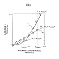
- Figure 4 is a graph illustrating the relationship between a light irradiation intensity I r and the light absorption intensity I a per unit time.
- S304 the relationship as illustrated in FIG. 4 is measured.
- the relationship between the light absorption characteristic and the light irradiation intensity per unit time when the sample 8 is composed of silicon (Si) and silicon nitride (SiN) is illustrated.
- the absorption characteristics 41 of silicon when the light irradiation intensity I r per unit time is about 150MW / cm 2 / ⁇ s, it can be seen that the light absorption intensity I a is changed from the linear characteristic to the nonlinear characteristics.
- the absorption characteristics 42 of silicon nitride maintains a linear characteristic to the light irradiation intensity I r of about 300MW / cm 2 / ⁇ s.
- the control messenger unit 22 sets the irradiation intensity at which the absorption characteristic 41 (Si) changes from linear to non-linear as the threshold value Irth (Si), and sets the irradiation intensity at which the absorption characteristic 42 (SiN) changes from linear to non-linear as the threshold value. It can be Threshold (SiN) . The significance of these threshold values will be described with reference to FIG.
- Figure 5 is a graph showing the relationship between the light irradiation intensity I r and the secondary electron emission amount per unit time.
- I r 2 electron emission amount 51 of silicon is increased and decreased gradually when I r reaches about 150MW / cm 2 / ⁇ s or more.
- the secondary electron emission amount 52 of silicon nitride increases to about 300 MW / cm 2 / ⁇ s.
- this phenomenon of increasing / decreasing the amount of secondary electron emission is referred to as a secondary electron modulation effect.
- the irradiation intensity at which the amount of secondary electron emission begins to decrease corresponds to the threshold value I th (Si) and the threshold value I th (SiN) , respectively.
- the three observation conditions for comparing the contrast are the condition a (0 MW / cm 2 / ⁇ s), the condition b (70 MW / cm 2 / ⁇ s), and the condition c (350 MW / cm 2 / ⁇ s), respectively. I set three. Examples of observation images using these will be described later.
- FIG. 6 is an example of a GUI (Graphical User Interface) 61 displayed by the image display unit 25.
- the accelerating voltage 62, the irradiation current 63, the magnification 64, and the scanning speed 65 which are the basic observation conditions, can be set.
- the image display unit 66 displays an observation image.
- the irradiation condition setting unit 67 obtains (a) a wavelength setting unit 68 for setting the wavelength of the optical pulse, (b) an absorption characteristic analysis unit 69 for acquiring (or calling from a database) the absorption characteristics of the sample, and (c) an absorption characteristic.
- Absorption characteristic display unit 70 to be displayed, (d) Based on the light irradiation intensity condition per unit time determined on the absorption characteristic display unit 70, the average output 71 of the optical pulse, the pulse width 72, the frequency 73 of the optical pulse, and the light. It has an irradiation intensity setting unit for setting a pulse irradiation diameter 74. In FIG. 6, two wavelengths can be selected as the optical pulse wavelength. Further, three conditions can be set as the light irradiation intensity condition per unit time. Parameters other than these may be set on the GUI 61.
- FIG. 7 is an example of a cross-sectional view of the sample 8.
- an example composed of silicon 75 and silicon nitride 76 is shown as described with reference to FIG.
- a thin film of silicon nitride 76 is patterned in a line on the silicon 75.
- the electron beam observation conditions are an acceleration voltage of 0.5 kV, an irradiation current of 100 pA, an observation magnification of 100 K times, and a scanning speed of TV scanning speed.
- the wavelength of the optical pulse is 355 nm.
- the light average output is 0 mW, 44 mW, and 220 mW for each irradiation intensity, respectively.
- FIG. 8 is an example of an observation image acquired under three light irradiation intensity conditions per unit time.
- Each of the conditions a to c is as described in FIG.
- the silicon 75 and the silicon nitride 76 show the same image brightness, and the visibility of the pattern is low.
- the observation image acquired under the condition b high image brightness is obtained for both silicon 75 and silicon nitride 76, and the visibility of the pattern is also high.
- the image brightness of the silicon 75 is low, and the image brightness of the silicon nitride 76 is high. It can be seen that the observation image acquired under the condition c can obtain the highest contrast.
- the charged particle beam device 1 according to the first embodiment is also a retarding system in which a voltage is applied to the XYZ stage 6, the material holder 7, and the sample 8 to reduce the electron energy applied to the sample. The same effect can be obtained even if it is carried out.
- the charged particle beam device 1 adjusts the irradiation intensity of the light actually irradiated per unit time according to the light absorption characteristic depending on the light irradiation intensity per unit time, so that the sample 8
- the amount of secondary electrons emitted from can be controlled. Therefore, even if the same type of material has similar absorption characteristics with respect to the light wavelength, the observed image contrast can be emphasized, so that the visibility of defects and patterns of the sample 8 is improved.
- FIG. 9 is a configuration diagram of the charged particle beam device 1 according to the second embodiment.
- the charged particle beam device 1 according to the second embodiment includes a photoelectron detector 91, a photovoltaic current measuring device 92, a circuit breaker 93, and a signal corrector 94 in addition to the configuration described in the first embodiment.
- the photoelectron detector 91 detects photoelectrons from the sample 8 by light pulse irradiation.
- the photovoltaic current measuring device 92 measures the current flowing through the sample 8 by irradiating the sample 8 with light.
- the circuit breaker 93 has a function of blocking an electron beam.
- the signal corrector 94 corrects the brightness of the secondary electron detection signal or the observed image based on the photoelectron detection signal detected by the photoelectron detector 91. Since other configurations are the same as those in the first embodiment, the differences will be mainly described below.
- FIG. 10 is a flowchart illustrating a procedure in which the charged particle beam device 1 acquires an observation image of the sample 8.
- S1002 is added between S307 and S308 in addition to the one described in FIG. 3, and S304 is replaced with S1001.
- Other steps are the same as in FIG.
- the control messenger unit 22 measures the light absorption characteristics of the sample 8 while changing the irradiation intensity of the light per unit time.
- the light absorption characteristic can be measured based on the amount of photoelectron emission detected by the photoelectron detector 91 or the photovoltaic current measured by the photovoltaic current measuring device 92.
- the relationship between the amount of photoelectron emission and the amount of light absorption, or the relationship between the photovoltaic current and the amount of light absorption may be measured in advance and the measurement result may be stored in the storage device 27.
- the signal corrector 94 corrects the detection signal of secondary electrons based on the light absorption characteristics measured in S1001. That is, the secondary electron detection signal when the sample 8 is irradiated with light and the electron beam is not irradiated is subtracted from the secondary electron detection signal when the sample 8 is irradiated with the electron beam and light. By doing so, the influence of light irradiation on the secondary electron detection signal is removed.
- the secondary electron detection signal when the sample 8 is irradiated with light and not irradiated with an electron beam can be acquired from the detection result in S1001.
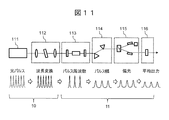
- FIG. 11 is a configuration diagram of the pulse laser 10 and the light intensity adjusting unit 11 in the second embodiment.
- the laser oscillator (or laser amplifier) 111 emits an optical pulse.
- the wavelength converter 112 is composed of a nonlinear optical element or the like, and controls the wavelength of an optical pulse.
- the pulse picker 113 is composed of an electro-optical effect element and a magneto-optical effect element, and controls the frequency of an optical pulse.
- the pulse dispersion controller 114 is composed of a pair of prisms or the like, and controls the pulse width of the optical pulse.
- the polarization controller 115 is configured by using a birefringent element or the like, and controls the polarization plane of the light pulse.
- the average output controller 116 is composed of an ND (Neutral Density) filter or the like whose density can be changed, and adjusts the average output of light pulses. Further, the light pulse introduction unit 12 can be configured by a zoom lens or the like, whereby the irradiation diameter of the light pulse can be controlled.
- ND Neutral Density
- FIG. 12 is an example of the relationship between the light absorption characteristics measured by S1001 and the light irradiation intensity per unit time.
- the absorption characteristics of P-type silicon and N-type silicon having different types of impurities were analyzed.
- the measurement was carried out by detecting photoelectrons using a photoelectron detector 91.
- the electron beam was cut off by the circuit breaker 93.
- the wavelength of the optical pulse is 405 nm. At this wavelength, it does not have photoenergy (eV) that reaches the vacuum level of silicon, so it does not emit photoelectrons when the light pulse is linearly absorbed.
- photoelectrons are emitted through multiphoton absorption, which is a non-linear process.
- Figure 12 shows the relationship between the emission intensity S ph of the light irradiation intensity I r and photoelectrons per unit time in P-type silicon and N-type silicon.
- the P-type silicon 121 emits photoelectrons with a light irradiation intensity of 4 MW / cm 2 / ⁇ s per unit time as a threshold value
- the N-type silicon 122 emits photoelectrons with a threshold value of 12 MW / cm 2 / ⁇ s.
- FIG. 12 shows an example of photoelectrons detected by using the photoelectron detector 91. However, when the photovoltaic current measuring device 92 is used, the photoelectron current emitted from the sample 8 can be measured. The same threshold value as above can be extracted.
- FIG. 13 is an example of a cross-sectional view of sample 8.
- N-type silicon 132 is bonded and formed on the surface of the P-type silicon 131, and a hole pattern of the silicon oxide film 133 is further formed on the N-type silicon 132.
- the defect 134 is a portion where the N-type silicon 132 and the hole pattern of the silicon oxide film 133 are out of alignment.
- the SEM observation conditions were an acceleration voltage of 1.0 kV, an irradiation current of 500 pA, an observation magnification of 200 K times, and a scanning speed of twice the TV scanning speed.
- the condition a of the light irradiation intensity per unit time was 0.0 MW / cm 2 / ⁇ s.
- Condition b was 4 MW / cm 2 / ⁇ s.
- the condition c was 12 MW / cm 2 / ⁇ s.
- Condition b further had an optical pulse frequency of 100 MHz, an average output of 16 mW, a pulse width of 1000 femtoseconds, and an irradiation diameter of 50 ⁇ m.
- the condition c was further set to an optical pulse frequency of 50 MHz, an average output of 54 mW, a pulse width of 800 femtoseconds, and an irradiation diameter of 60 ⁇ m.
- FIG. 14 is a graph showing the relationship between the correction amount ⁇ C of the secondary electron detection signal and the light irradiation intensity per unit time in the second embodiment.
- Correction amount ⁇ C in addition to the relationship between the emission intensity S ph of the light irradiation intensity I r and photoelectrons per unit time as shown in FIG. 12 was determined by the area ratio of the P-type silicon 131 and the N-type silicon 132 in the sample 8 .. In the second embodiment, this ratio is set to 50%.
- FIG. 15 is an example of an observation image acquired under three light irradiation intensity conditions per unit time.
- the P-type silicon 131 and the N-type silicon 132 show the same image brightness, the visibility of the pattern is low, and the defective portion cannot be visually recognized.
- the observation image acquired under the condition b the visibility of the P-type silicon 131 and the N-type silicon 132 is improved, but it is insufficient for defect detection.
- the image brightness of the P-type silicon 131 is low, and the pattern contrast is the highest.
- the defect 156 can be sufficiently visually recognized if the observation image is obtained under the condition c.
- the charged particle beam device 1 detects secondary electrons by removing the influence of photoelectrons emitted from the sample 8 by irradiating the sample 8 with light from the secondary electron detection signal. Correct the signal. As a result, the contrast of the observed image of the sample 8 can be formed more accurately, so that the visibility of defects and patterns can be improved.
- FIG. 16 is a time chart showing each of electron beam irradiation timing, pulse laser irradiation timing, and secondary electron detection timing.
- the control messenger unit 22 controls the electron beam irradiation period 161 and the interval period 162 by controlling the circuit breaker 93.
- the optical pulse 163 of the pulse laser is controlled at a constant frequency regardless of the irradiation period 161 and the interval period 162.
- the light pulse 163 may be irradiated in synchronization with the irradiation period 161 or may be irradiated in synchronization with the interval period 162.
- the timing 164 for detecting the secondary electrons is synchronized with the irradiation period 161.
- the timing 164 for detecting the secondary electrons needs to be synchronized with the irradiation period 161 in consideration of the traveling time of the secondary electrons and the delay time based on the circuit delay of the electron detector 5.
- FIG. 17 is an example of the GUI 61 displayed by the image display unit 25 in the third embodiment.
- an irradiation period setting unit 171 and an interval period setting unit 172 are added.
- FIG. 18 is an example of a cross-sectional view of sample 8.
- N-type silicon 182 is joined and formed on the surface of the P-type silicon 181. Further, a silicon oxide film 183 is arranged on the silicon oxide film 183, and a hole pattern is formed on the silicon oxide film 183.
- Polysilicon contact plug 184 is formed in the hole pattern.
- Defect 185 is a high concentration of N-type silicon injected.
- the defect 186 is a thin residual film between the contact plug 184 and the N-type silicon 182.
- Defect 187 has a thicker residual film than Defect 186.
- the observation conditions were an acceleration voltage of 0.3 kV, an irradiation current of 50 pA, an observation magnification of 50 K times, and a scanning speed of TV scanning speed.
- the irradiation time was 200 ns and the interval time was 3.2 ⁇ s when the electron beam was irradiated intermittently.
- the relationship between the light absorption characteristics of the sample 8 and the light irradiation intensity per unit time was acquired by using the photovoltaic current measuring device 92.
- conditions a to c were set as the light irradiation intensity per unit time based on the absorption characteristics.
- Condition a is 0.0 MW / cm 2 / ⁇ s.
- Condition b is 16 MW / cm 2 / ⁇ s.
- Condition c is 30 MW / cm 2 / ⁇ s.
- Each condition corresponding to this was set in the irradiation condition setting unit 67.
- FIG. 19 is an example of an observation image acquired by an electron beam under each irradiation condition.
- the contact plug 192 can be identified, but the defect cannot be identified.
- the depletion layer of the junction is made conductive by the linear absorption of the light pulse, so that the normal contact plug 194 becomes bright.
- defects having a high concentration of N-type silicon with weak linear absorption defects 185 in FIG. 18
- defects having a residual film defects 186 and 187 in FIG.
- the difference image 200 is formed by the difference between the two observation images (condition b: 5 ⁇ s) (condition c: 5 ⁇ s) in the middle of FIG. From the difference image 200, a bonding defect on the bottom of the contact plug can be extracted.
- the difference image 201 is formed by the difference between the two observation images (condition c: 5 ⁇ s) (condition c: 200 ns) in the lower part of FIG. From the difference image 201, residual film defects having different film thicknesses on the bottom of the contact plug can be extracted.
- the charged particle beam device 1 switches between a period in which the sample 8 is irradiated with an electron beam and a period in which the sample 8 is not irradiated, so that the sample 8 is intermittently irradiated with the electron beam while observing an image. To generate. As a result, it is possible to obtain an observation image having a contrast different from that obtained while continuously irradiating the sample 8 with an electron beam. By utilizing this, it is possible to discriminate and detect electrical defects having different electrical characteristics.
- FIG. 20 is a configuration example of the absorption characteristic measuring unit 13.
- the light pulse reflected by the sample 8 is elliptically polarized by the wave plate 211, and is divided into S-polarized light and P-polarized light by the birefringent element 212.
- the photodetector 213 detects the light intensity of S-polarized light
- the photodetector 214 detects the light intensity of P-polarized light.
- the subtractor 215 calculates the difference between the light intensity of S-polarized light and the light intensity of P-polarized light.
- the signal detector 216 converts the calculation result into data as the intensity of elliptically polarized light. Digital processing may be used instead of the analog circuit to obtain the difference signal.
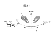
- FIG. 21 is a configuration example of the absorption characteristic measuring unit 13.
- the harmonic optical pulse generated in the sample 8 is spectrally decomposed by the diffraction grating 217.
- the light intensity for each spectrum is detected by the light intensity sensor 218 having a plurality of detection elements created by the silicon process on the line.
- the light intensity of each wavelength obtained by the light intensity sensor 218 is digitized by the signal detector 219.
- the light pulse to be irradiated is circularly polarized light, and the wavelength is 700 nm.
- the threshold value of the light irradiation intensity per unit time, which changes from linear to non-linear, is the irradiation intensity changing to elliptical polarization or the irradiation intensity generated by the second harmonic, 350 nm.
- the flowchart of FIG. 3 and the GUI of FIG. 6 are used.
- a sample formed of an organic-inorganic hybrid material in which a dielectric is mixed with an organic substance was used.
- Conditions a to c were set as the light irradiation intensity per unit time depending on the change in the polarization plane from the sample 8 due to the light pulse irradiation or the threshold value of the light irradiation intensity per unit time in which the second harmonic generation is generated.
- Condition a is 0.0 MW / cm 2 / ⁇ s.
- Condition b is 4 MW / cm 2 / ⁇ s.
- Condition c is 10 MW / cm 2 / ⁇ s.
- Condition b further had an optical pulse frequency of 100 MHz, an average output of 14 mW, a pulse width of 220 femtoseconds, and an irradiation diameter of 100 ⁇ m.
- the condition c was further set to an optical pulse frequency of 100 MHz, an average output of 35 mW, a pulse width of 220 femtoseconds, and an irradiation diameter of 100 ⁇ m.
- FIG. 22 is an example of an observation image acquired under three light irradiation intensity conditions per unit time.
- the organic substance 222 and the dielectric 223, which are the bases of the hybrid material show the same image brightness, and the visibility of the dielectric domain is low.
- the observation image acquired under condition b since the dielectric is excited by linear absorption, secondary electron emission from the dielectric 225 increases, and the dielectric domain can be clearly seen.
- the observation image of condition c non-linear absorption occurs in each of the dielectrics having different complex permittivity, so that the emission of secondary electrons is reduced.
- the dielectrics 227 having different complex dielectric constants can be inspected on a gray scale according to the difference in the complex dielectric constant.
- the domains of the sample 8 having different dielectric constants can be discriminated and detected.
- the fourth embodiment two configuration examples for detecting the polarization plane and the wavelength are shown as the absorption characteristic measurement unit 13, but it is not necessary to detect both of these two characteristics, and the polarization plane may be detected.
- the wavelength may be detected.
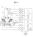
- FIG. 23 is a configuration diagram of the charged particle beam device 1 according to the fifth embodiment.
- a configuration example including an energy filter 231 for discriminating the energy of secondary electrons and an energy filter control unit 232 for controlling the voltage applied to the energy filter 231 is shown.
- the user specifies a voltage to be applied to the energy filter 231 via the operation interface 23, and the energy filter control unit 232 controls the voltage according to the designation.
- an energy spectroscope such as a spectrum meter using a Vienna filter may be used.
- the sample 8 shown in FIG. 7 was used.
- the observation conditions are an accelerating voltage of 0.5 kV, an irradiation current of 100 pA, an observation magnification of 100 K times, and a scanning speed of TV scanning speed.
- the optical pulse wavelength is 355 nm.
- the conditions a and b were set as the light irradiation intensity based on the relationship between the absorption characteristics and the light irradiation intensity per unit time as in the first embodiment.
- the condition a was 0 MW / cm 2 / ⁇ s
- the condition b was 350 MW / cm 2 / ⁇ s.
- the average output was adjusted based on the set light irradiation intensity conditions per unit time.
- the average output is 0 mW and 220 mW, respectively.
- FIG. 24 is a graph showing the energy distribution of secondary electrons when a light pulse is irradiated according to each light irradiation intensity.
- a light pulse of 0 MW / cm 2 / ⁇ s that is, no light is irradiated
- silicon 241 and silicon nitride 242 there is almost no difference between silicon 241 and silicon nitride 242.
- an optical pulse of 350 MW / cm 2 / ⁇ s the silicon nitride is in a linearly absorbed state, and the efficiency of secondary electron emission is high. It can be seen that the energy distribution of the secondary electrons of silicon nitride 243 in this state has a high peak intensity and the peak is shifted to the low energy side.
- Silicon irradiated with an optical pulse of 350 MW / cm 2 / ⁇ s is in a non-linear absorption state, and secondary electron emission is suppressed. It can be seen that the energy distribution of the secondary electrons of silicon 244 in this state has a low peak intensity and the peak is shifted to the high energy side. From FIG. 24, it can be seen that in addition to the difference in secondary electron emission efficiency, the difference in secondary electron yield can be expanded by the energy filter 231.
- the filter voltage VEF is set to 4V.
- FIG. 25 is an example of the light irradiation intensity conditions per unit time and the observation image acquired by the energy filter 231.
- the silicon 252 and the silicon nitride 253 show the same image brightness, and the visibility of the pattern is low.
- the difference in image brightness between the silicon 252 and the silicon nitride 253 is widened, and the visibility of the pattern is improved.
- the image contrast between the silicon 252 and the silicon nitride 253 was improved by the energy discrimination, and the visibility of the pattern was further improved. You can see that.
- ⁇ Embodiment 5 Summary> According to the charged particle beam apparatus 1 according to the fifth embodiment, in addition to adjusting the light irradiation intensity per unit time described in the first to fourth embodiments, observation is performed by using energy discrimination of secondary electrons. The contrast of the image can be emphasized.
- FIG. 26 is a block diagram of the charged particle beam device 1 according to the sixth embodiment of the present invention.
- a configuration example for identifying the characteristics of the sample 8 by using the secondary electron detection signal or the observation image itself will be described instead of using the absorption characteristic measurement unit 13 and the absorption characteristic measurement control unit 21. ..
- the configuration shown in FIG. 26 is the same as the configuration described in the first embodiment except that the absorption characteristic measurement unit 13 and the absorption characteristic measurement control unit 21 are not provided.
- condition a and the condition b are set as the light irradiation intensity condition per unit time.
- Condition a is 10.0 MW / cm 2 / ⁇ s.
- Condition b is 100 MW / cm 2 / ⁇ s.
- the condition a was further set to an optical pulse average output of 400 mW.
- Condition b was further set to an optical pulse average output of 4000 mW.
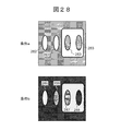
- FIG. 27 is an example of a cross-sectional view of sample 8.
- N-type silicon 272 having a low concentration and N-type silicon 273 having a high concentration are formed on the surface of the P-type silicon 271.
- a low-concentration N-type silicon well 274 is further formed on the surface of the P-type silicon 271.
- low-concentration P-type silicon 275 and high-concentration P-type silicon 276 are formed on the surface of the N-type silicon well 274.
- FIG. 28 is an example of an observation image acquired under two light irradiation intensity conditions.
- the N-type silicon 282 and the P-type silicon 283 can be clearly distinguished.
- the type of impurities and the energy band of the material can be known.
- the difference in density can be identified from the difference in image brightness between the low density N-type silicon 285 and the high density N-type silicon 286.
- the low-density P-type silicon 287 and the high-density P-type silicon 288 can be identified from the difference in image brightness.
- the concentration of impurities and the electronic state of the material can be known.
- the charged particle beam apparatus 1 According to the charged particle beam apparatus 1 according to the sixth embodiment, it is possible to discriminate and visualize the different types of features of the sample 8 from the observation images acquired under the light irradiation intensity conditions per unit time.
- the present invention is not limited to the above-described embodiment, and includes various modifications.
- the above-described embodiment has been described in detail in order to explain the present invention in an easy-to-understand manner, and is not necessarily limited to the one including all the described configurations.
- it is possible to replace a part of the configuration of one embodiment with the configuration of another embodiment and it is also possible to add the configuration of another embodiment to the configuration of one embodiment.
- one or more wavelengths can be selected by using a tunable laser whose wavelength can be selected by parametric oscillation.
- a single wavelength pulse laser may be used, or a wavelength conversion unit that generates harmonics of light may be used. Since an image with uniform image contrast can be obtained in the irradiation region of the light pulse, it is desirable that the irradiation region of the light pulse is wider than the deflection region of the electron beam controlled by the deflector 3, but the present invention has the light pulse. It is not limited to the difference between the irradiation region and the deflection region.
- the optical pulse and the electron beam may be irradiated at the same time in time, or may be irradiated at different timings in time.
- an ND filter capable of varying the density for controlling the average output of the laser can be used.
- an optical attenuator can be used as an optical system for controlling the average output.
- the following can also be used as the light intensity adjusting unit 11: (a) The frequency of the pulse and the number of pulse irradiations are controlled by using an electro-optical effect element or a pulse picker using a magnetic-optical effect element, etc. b) The pulse width is controlled by using a pulse dispersion control optical system composed of a pair of prisms, and (c) the irradiation region of an optical pulse is controlled by using a condenser lens.
- an optical branching element, a pulse stocker, an optical wavelength conversion element, a polarization control element, and the like can also be used. These can also be used in combination.
- the absorption intensity is obtained from the difference signal between the irradiation light and the reflected light as the light absorption characteristic, but the light intensity of the reflected light may be used.
- the difference may be obtained by digital processing instead of the analog circuit.
- the photoelectron detector 91 can be shared with the electron detector 5.
- the photoelectron detector 91 and the photovoltaic current measuring device 92 are used in combination as means for measuring the photoelectrons from the sample 8, but only one of them may be used.
- the absorption characteristic measuring unit 13 a reflected light detector from the sample 8, a polarizing surface detector of the reflected light from the sample 8, a wavelength detector of the reflected light from the sample 8, and the like can also be used.
- the circuit breaker 93 can be configured by an electron beam blocking means composed of a parallel electrode and a diaphragm.
- the deflector 3 may block the electron beam, or a shield such as a valve on the optical axis of the electron beam may be operated.
- control messenger unit 22 can be configured by using hardware such as a circuit device that implements the function, or by executing software that implements the function by an arithmetic unit. You can also.
- Each functional unit controlled by the control messenger unit 22 (electron gun control unit 14, deflection signal control unit 15, electronic lens control unit 16, detector control unit 17. stage position control unit 18, pulse laser control unit 19, light intensity adjustment The same applies to the control unit 20, the absorption characteristic measurement control unit 21, etc.). The same applies to the image forming unit 24.
- the present invention describes the other charged particle beam devices. Can also be used. That is, the present invention can be applied to other charged particle beam devices that adjust the emission efficiency of secondary charged particles by irradiating the sample 8 with light.
Abstract
Description
以下ではまず本発明の基本原理について説明し、次に本発明の具体的な実施形態について説明する。本発明は、観察する試料に対して光を照射することにより、試料内部でキャリアを励起させる。このとき試料は励起状態となる。励起状態下における2次電子の放出量は、光の吸収量に応じて増加する。一方、光照射によって試料から光電子が放出される場合、試料は電子が欠乏した空乏状態となる。空乏状態下における2次電子の放出量は、光の吸収量に応じて減衰する。 <About the basic principle of the present invention>
Hereinafter, the basic principle of the present invention will be described first, and then specific embodiments of the present invention will be described. In the present invention, carriers are excited inside the sample by irradiating the sample to be observed with light. At this time, the sample is in an excited state. The amount of secondary electrons emitted under the excited state increases according to the amount of light absorbed. On the other hand, when photoelectrons are emitted from the sample by light irradiation, the sample is in a depleted state in which electrons are deficient. The amount of secondary electrons emitted under the depleted state is attenuated according to the amount of light absorbed.
本発明の実施形態1では、試料が有する光吸収特性に応じて単位時間当たりの光照射強度を制御したパルスレーザを観察領域に照射し、観察像コントラストを強調する荷電粒子線装置について述べる。 <
In the first embodiment of the present invention, a charged particle beam device that irradiates the observation region with a pulsed laser in which the light irradiation intensity per unit time is controlled according to the light absorption characteristics of the sample to emphasize the observation image contrast will be described.
ステージ機構系は、試料8を観察位置に移動させる(S301)。制御伝令部22は、操作インターフェース23からの指定入力にしたがって、基本的な電子線の観察条件として加速電圧、照射電流、倍率、走査時間を設定する(S302)。パルスレーザ制御部19はパルスレーザの波長を設定する(S303)。レーザ波長は、試料8が光を吸収する波長帯に基づき設定することが望ましい。 (FIG. 3: Steps S301 to S303)
The stage mechanism system moves the
制御伝令部22は、光の単位時間当たりの照射強度を変化させながら、試料8による光の吸収特性を測定する。光照射強度は光強度調整部11によって制御する。光吸収測定は吸収特性測定部13によって測定する。制御伝令部22は、測定結果に基づき、光照射強度と光吸収特性との間の対応関係を記述したデータを記憶装置27に格納する。本ステップにおける対応関係の例については後述の図4で説明する。 (FIG. 3: Step S304)
The
制御伝令部22は、ステップS304の結果に基づき、単位時間当たりの光照射強度の閾値を設定する。ここでいう閾値は、例えば式2の光吸収特性のうち線形吸収項(α1)と非線形吸収項(α2以降)いずれが支配的であるかに基づき定めることができる。閾値を決定する基準の具体例については、後述の図4で説明する。 (Fig. 3: Step S305)
The
本フローチャートにおいては、S304における解析結果を記憶装置27に格納してこれを用いることとしたが、あらかじめ多様な条件における光照射強度と光吸収特性との間の対応関係を解析してその結果をデータベースとして記憶装置27に格納しておくこともできる。これにより、観察像を取得するごとにステップS304~S305を実施する必要はなくなる。 (Fig. 3: Steps S304 to S305: Supplement 1)
In this flowchart, the analysis result in S304 is stored in the
記憶装置27は、測定結果や対応関係を記憶する適当な装置によって構成することができる。例えば測定結果や対応関係をデータベースとして保持しておきこれを利用するのであれば、不揮発性記憶装置によって記憶装置27を構成することができる。本フローチャートを実施するごとに測定結果と対応関係を取得するのであれば、これらを一時的に記憶するメモリデバイスなどによって記憶装置27を構成することができる。これらを組み合わせてもよい。 (Fig. 3: Steps S304 to S305: Supplement 2)
The
制御伝令部22は、S304~S305の結果にしたがって、1つ以上の光照射強度を観察条件として設定する(S306)。ここでいう観察条件は、S305において設定した閾値そのものである必要はなく、後述するように閾値前後の適当な値でもよい。制御伝令部22は、観察条件として設定した光照射強度となるように、光強度調整部11によって照射強度を調整する(S307)。制御伝令部22は、単位時間当たりの照射強度を調整した光パルスと電子線を試料8に照射し、画像形成部24によって観察像を取得する(S308)。 (FIG. 3: Steps S306 to S308)
The
本実施形態1に係る荷電粒子線装置1は、単位時間当たりの光照射強度に依拠する光吸収特性に応じて、実際に照射する光の単位時間当たりの照射強度を調整することにより、試料8から放出される2次電子量を制御することができる。したがって光波長に対する吸収特性が近い同種の材料であっても、観察像コントラストを強調することができるので、試料8が有する欠陥やパターンの視認性が向上する。 <Embodiment 1: Summary>
The charged
試料8に対して光を照射すると、試料8から光電子が放出される場合がある。この光電子は2次電子に対するノイズとして作用する。そこで本発明の実施形態2では、2次電子の検出結果に対して光電子が与える影響を除去する構成例について説明する。 <
When the
制御伝令部22は、光の単位時間当たりの照射強度を変化させながら、試料8による光の吸収特性を測定する。光吸収特性は、光電子検出器91が検出する光電子放出量、または光起電流測定器92が測定する光起電流に基づき測定することができる。光電子放出量と光吸収量の関係、または光起電流と光吸収量の関係は、例えばあらかじめ測定してその測定結果を記憶装置27に格納しておけばよい。 (FIG. 10: Step S1001)
The
信号補正器94は、S1001において測定した光吸収特性に基づき、2次電子の検出信号を補正する。すなわち、試料8に対して電子線と光を照射しているときにおける2次電子検出信号から、試料8に対して光を照射し電子線を照射していないときにおける2次電子検出信号を減算することにより、光照射が2次電子検出信号に対して与える影響を除去する。試料8に対して光を照射し電子線を照射していないときにおける2次電子検出信号は、S1001における検出結果によって取得することができる。 (FIG. 10: Step S1002)
The
本実施形態2に係る荷電粒子線装置1は、試料8に対して光を照射することにより試料8から放出される光電子の影響を、2次電子検出信号から除去することにより、2次電子検出信号を補正する。これにより、試料8の観察像コントラストをより正確に形成することができるので、欠陥やパターンの視認性を向上させることができる。 <Embodiment 2: Summary>
The charged
本発明の実施形態3では、試料8に対して電子線を断続的に照射する例について説明する。電子線を照射しているときと照射していないときそれぞれの観察像を比較することにより、試料8の視認性を向上させることができる。荷電粒子線装置1の構成は実施形態2と同様である。遮断器93が電子線を遮断することにより、電子線の照射期間と非照射期間(間隔期間)を制御できる。 <
In the third embodiment of the present invention, an example of intermittently irradiating the
本実施形態3に係る荷電粒子線装置1は、試料8に対して電子線を照射する期間と照射しない期間を切り替えることにより、試料8に対して断続的に電子線を照射しながら、観察像を生成する。これにより、試料8に対して連続的に電子線を照射しながら取得した観察像とは異なるコントラストを有する観察像を得ることができる。このことを利用して、電気特性の異なる電気的な欠陥を弁別して検出できる。 <Embodiment 3: Summary>
The charged
図20は、吸収特性測定部13の構成例である。ここでは光の偏光面を検出する構成を示した。試料8で反射した光パルスは、波長板211によって楕円偏光となり、複屈折素子212によってS偏光とP偏光に分けられる。光検出器213はS偏光の光強度を検出し、光検出器214はP偏光の光強度を検出する。減算器215は、S偏光の光強度とP偏光の光強度の差分を演算する。信号検出器216はその演算結果を楕円偏光の強度としてデータ化する。差分信号を求めるために、アナログ回路に代えてデジタル処理を用いてもよい。 <Embodiment 4>
FIG. 20 is a configuration example of the absorption
本発明の実施形態5では、実施形態1~4で説明した構成に加えて、2次電子のエネルギ弁別によって観察像のコントラストを強調する構成例について述べる。その他構成は実施形態1~4と同様である。 <
In the fifth embodiment of the present invention, in addition to the configurations described in the first to fourth embodiments, a configuration example in which the contrast of the observed image is emphasized by energy discrimination of secondary electrons will be described. Other configurations are the same as those of the first to fourth embodiments.
本実施形態5に係る荷電粒子線装置1によれば、実施形態1~4で説明した単位時間当たりの光照射強度を調整することに加えて、2次電子のエネルギ弁別を用いることにより、観察像のコントラストを強調することができる。 <Embodiment 5: Summary>
According to the charged
図26は、本発明の実施形態6に係る荷電粒子線装置1の構成図である。本実施形態6においては、吸収特性測定部13と吸収特性測定制御部21を用いることに代えて、2次電子検出信号または観察像そのものを用いて試料8の特徴を識別する構成例について説明する。図26に示す構成は、吸収特性測定部13と吸収特性測定制御部21を備えていないことを除き、実施形態1で説明した構成と同様である。 <Embodiment 6>
FIG. 26 is a block diagram of the charged
本発明は、前述した実施形態に限定されるものではなく、様々な変形例が含まれる。例えば、上記した実施形態は本発明を分かりやすく説明するために詳細に説明したものであり、必ずしも説明した全ての構成を備えるものに限定されるものではない。また、ある実施形態の構成の一部を他の実施形態の構成に置き換えることが可能であり、また、ある実施形態の構成に他の実施形態の構成を加えることも可能である。また、各実施形態の構成の一部について、他の構成の追加・削除・置換をすることが可能である。 <About a modified example of the present invention>
The present invention is not limited to the above-described embodiment, and includes various modifications. For example, the above-described embodiment has been described in detail in order to explain the present invention in an easy-to-understand manner, and is not necessarily limited to the one including all the described configurations. Further, it is possible to replace a part of the configuration of one embodiment with the configuration of another embodiment, and it is also possible to add the configuration of another embodiment to the configuration of one embodiment. Further, it is possible to add / delete / replace a part of the configuration of each embodiment with another configuration.
2 電子銃
3 偏向器
4 電子レンズ
5 電子検出器
6 XYZステージ
7 試料ホルダ
8 試料
9 筐体
10 パルスレーザ
11 光強度調整部
12 光パルス導入部
13 吸収特性測定部
14 電子銃制御部
15 偏向信号制御部
16 電子レンズ制御部
17 検出器制御部
18 ステージ位置制御部
19 パルスレーザ制御部
20 光強度調整制御部
21 吸収特性測定制御部
22 制御伝令部
23 操作インターフェース
24 画像形成部
25 画像表示部
30 ビームスプリッタ
31 照射光検出器
32 反射光検出器
33 減算器
34 信号検出器
51 シリコン
52 窒化シリコン
61 GUI
66 画像表示部
67 照射条件設定部
68 波長設定部
69 吸収特性解析部
70 吸収特性表示部
75 シリコン
76 窒化シリコン
91 光電子検出器
92 光起電流測定器
93 遮断器
94 信号補正器
111 レーザ発振器(あるいはレーザ増幅器)
112 波長変換器
113 パルスピッカー
114 パルス分散制御器
115 偏光制御器
116 平均出力制御器
121 P型シリコン
122 N型シリコン
131 P型シリコン
132 N型シリコン
133 シリコン酸化膜
134 欠陥
152 P型シリコン
153 N型シリコン
156 欠陥
161 照射期間
162 間隔期間
163 光パルス
171 照射期間設定部
172 間隔期間設定部
181 P型シリコン
182 N型シリコン
183 シリコン酸化膜
184 コンタクトプラグ
185 欠陥
186 欠陥
187 欠陥
192 コンタクトプラグ
194 コンタクトプラグ
196 欠陥
198 欠陥
199 欠陥
200 差画像
201 差画像
211 波長板
212 複屈折素子
213 光検出器
214 光検出器
215 減算器
216 信号検出器
217 回折格子
218 光強度センサ
219 信号検出器
222 有機物
223 誘電体
225 誘電体
227 誘電体
231 エネルギフィルタ
232 エネルギフィルタ制御部
252 シリコン
253 窒化シリコン
271 P型シリコン
272 N型シリコン
273 N型シリコン
274 N型シリコンウェル
275 P型シリコン
276 P型シリコン
282 N型シリコン
283 P型シリコン
285 N型シリコン
286 N型シリコン
287 P型シリコン
288 P型シリコン 1 Charged
66
112
Claims (13)
- 試料に対して荷電粒子線を照射する荷電粒子線装置であって、
前記試料に対して1次荷電粒子を照射する荷電粒子源、
前記試料に対して照射する光を出射する光源、
前記1次荷電粒子を前記試料に対して照射することにより前記試料から生じる2次荷電粒子を検出する検出器、
前記検出器が検出した前記2次荷電粒子を用いて前記試料の観察像を生成する画像処理部、
前記光の単位時間当たりの照射強度を調整する光強度制御部、
を備え、
前記光強度制御部は、前記光の単位時間当たりの照射強度を変化させることにより、それぞれ異なるコントラストを有する複数の前記観察像を前記画像処理部に生成させる
ことを特徴とする荷電粒子線装置。 A charged particle beam device that irradiates a sample with a charged particle beam.
A charged particle source that irradiates the sample with primary charged particles,
A light source that emits light to irradiate the sample,
A detector that detects secondary charged particles generated from the sample by irradiating the sample with the primary charged particles.
An image processing unit that generates an observation image of the sample using the secondary charged particles detected by the detector.
A light intensity control unit that adjusts the irradiation intensity of light per unit time.
With
The light intensity control unit is a charged particle beam device that causes the image processing unit to generate a plurality of the observation images having different contrasts by changing the irradiation intensity of the light per unit time. - 前記試料は、前記光の単位時間当たりの照射強度に応じて、前記2次荷電粒子の放出量が変化する特性を有しており、
前記光強度制御部は、前記光の単位時間当たりの照射強度を第1強度に制御することにより、前記試料が前記第1強度に対応する第1放出量の前記2次荷電粒子を放出するようにした上で、前記観察像を前記画像処理部に生成させ、
前記光強度制御部は、前記光の単位時間当たりの照射強度を前記第1強度とは異なる第2強度に制御することにより、前記試料が前記第2強度に対応する第2放出量の前記2次荷電粒子を放出するようにした上で、前記観察像を前記画像処理部に生成させる
ことを特徴とする請求項1記載の荷電粒子線装置。 The sample has a characteristic that the amount of emitted secondary charged particles changes according to the irradiation intensity of the light per unit time.
The light intensity control unit controls the irradiation intensity of the light per unit time to the first intensity so that the sample emits the secondary charged particles of the first emission amount corresponding to the first intensity. Then, the observation image is generated in the image processing unit.
The light intensity control unit controls the irradiation intensity of the light per unit time to a second intensity different from the first intensity, so that the sample has a second emission amount corresponding to the second intensity. The charged particle beam apparatus according to claim 1, wherein the observation image is generated in the image processing unit after the next charged particles are emitted. - 前記光強度制御部は、前記光の単位時間当たりの照射強度を前記第1強度と前記第2強度との間の第3強度に制御することにより、前記試料が前記第3強度に対応する第3放出量の前記2次荷電粒子を放出するようにした上で、前記観察像を前記画像処理部に生成させ、
前記第3放出量は前記第1放出量よりも大きく、前記第2放出量は前記第1放出量よりも小さい
ことを特徴とする請求項2記載の荷電粒子線装置。 The light intensity control unit controls the irradiation intensity of the light per unit time to a third intensity between the first intensity and the second intensity, so that the sample corresponds to the third intensity. After the secondary charged particles of 3 emission amounts are emitted, the observation image is generated in the image processing unit.
The charged particle beam apparatus according to claim 2, wherein the third release amount is larger than the first release amount, and the second release amount is smaller than the first release amount. - 前記試料が前記光を吸収する吸収量は、前記光の単位時間当たりの照射強度の1乗に比例する第1成分と、前記光の単位時間当たりの照射強度の2乗以上のべき乗に比例する第2成分とを有しており、
前記第2成分は、前記光の単位時間当たりの照射強度が前記第3強度以上であるとき、前記第1成分以上となり、前記光の単位時間当たりの照射強度が前記第3強度未満であるとき、前記第1成分未満となり、
前記光強度制御部は、前記光の単位時間当たりの照射強度を前記第2強度にすることにより、前記吸収量のうち前記第2成分が前記第1成分よりも大きくなるようにし、
前記光強度制御部は、前記光の単位時間当たりの照射強度を前記第1強度にすることにより、前記吸収量のうち前記第1成分が前記第1成分よりも大きくなるようにする
ことを特徴とする請求項3記載の荷電粒子線装置。 The amount of absorption of the light by the sample is proportional to the first component proportional to the first power of the irradiation intensity per unit time of the light and the power of the square of the irradiation intensity per unit time of the light. It has a second component and
The second component is the first component or more when the irradiation intensity of the light per unit time is the third intensity or more, and the irradiation intensity of the light per unit time is less than the third intensity. , Less than the first component
The light intensity control unit sets the irradiation intensity of the light per unit time to the second intensity so that the second component of the absorbed amount becomes larger than the first component.
The light intensity control unit is characterized in that the first component of the absorbed amount is made larger than the first component by setting the irradiation intensity of the light per unit time to the first intensity. The charged particle beam apparatus according to claim 3. - 前記試料が前記光を吸収する吸収量は、前記光の単位時間当たりの照射強度の1乗に比例する第1成分と、前記光の単位時間当たりの照射強度の2乗以上のべき乗に比例する第2成分とを有しており、
前記光強度制御部は、前記吸収量のうち前記第2成分が前記第1成分よりも大きくなるように前記光の単位時間当たりの照射強度を制御することにより、前記第1成分が前記第2成分よりも大きいときと比較して、前記放出量が小さくなるようにする
ことを特徴とする請求項3記載の荷電粒子線装置。 The amount of absorption of the light by the sample is proportional to the first component proportional to the first power of the irradiation intensity per unit time of the light and the power of the square of the irradiation intensity per unit time of the light. It has a second component and
The light intensity control unit controls the irradiation intensity of the light per unit time so that the second component of the absorbed amount becomes larger than the first component, so that the first component becomes the second component. The charged particle beam apparatus according to claim 3, wherein the emission amount is made smaller than that when the component is larger than the component. - 前記荷電粒子線装置はさらに、前記試料が前記光を吸収する吸収量を測定する吸収特性測定部を備え、
前記荷電粒子線装置はさらに、前記吸収特性測定部が測定した前記吸収量と、前記光の単位時間当たりの照射強度との間の対応関係を記述した対応関係データを格納する記憶部を備え、
前記光強度制御部は、前記対応関係データが記述している前記対応関係にしたがって、前記第1強度と前記第2強度を決定する
ことを特徴とする請求項2記載の荷電粒子線装置。 The charged particle beam device further includes an absorption characteristic measuring unit for measuring the amount of absorption of the sample for absorbing the light.
The charged particle beam device further includes a storage unit that stores correspondence data that describes the correspondence between the absorption amount measured by the absorption characteristic measuring unit and the irradiation intensity of the light per unit time.
The charged particle beam device according to claim 2, wherein the light intensity control unit determines the first intensity and the second intensity according to the correspondence relationship described in the correspondence relationship data. - 前記荷電粒子線装置はさらに、前記吸収特性測定部が測定した前記吸収量にしたがって、前記検出器が検出した前記2次荷電粒子の信号量を補正する、信号量補正部を備える
ことを特徴とする請求項6記載の荷電粒子線装置。 The charged particle beam device further includes a signal amount correction unit that corrects the signal amount of the secondary charged particles detected by the detector according to the absorption amount measured by the absorption characteristic measuring unit. The charged particle beam apparatus according to claim 6. - 前記信号量補正部は、前記試料に対して前記光と前記1次荷電粒子を照射しているとき前記検出器が検出する前記2次荷電粒子の第1信号量から、前記試料に対して前記光を照射し前記1次荷電粒子を照射していないとき前記前記検出器が検出する前記2次荷電粒子の第2信号量を減算することにより、前記検出器による検出結果を補正する
ことを特徴とする請求項7記載の荷電粒子線装置。 The signal amount correction unit refers to the sample from the first signal amount of the secondary charged particles detected by the detector when the sample is irradiated with the light and the primary charged particles. It is characterized in that the detection result by the detector is corrected by subtracting the second signal amount of the secondary charged particles detected by the detector when the primary charged particles are not irradiated with light. The charged particle beam apparatus according to claim 7. - 前記光強度制御部は、前記試料に対して前記1次荷電粒子を照射する照射期間と、前記試料に対して前記1次荷電粒子を照射しない間隔期間とを切り替えることができるように構成されており、
前記画像処理部は、前記試料に対して前記1次荷電粒子を連続的に照射している間において前記試料の第1観察像を生成するとともに、前記照射期間と前記間隔期間を切り替えながら前記1次荷電粒子を断続的に照射している間において前記試料の第2観察像を生成することにより、それぞれ異なるコントラストを有する複数の前記観察像を生成する
ことを特徴とする請求項1記載の荷電粒子線装置。 The light intensity control unit is configured to be able to switch between an irradiation period in which the sample is irradiated with the primary charged particles and an interval period in which the sample is not irradiated with the primary charged particles. Ori
The image processing unit generates a first observation image of the sample while continuously irradiating the sample with the primary charged particles, and switches between the irradiation period and the interval period. The charge according to claim 1, wherein a plurality of the observation images having different contrasts are generated by generating a second observation image of the sample while the next charged particles are intermittently irradiated. Particle beam device. - 前記荷電粒子線装置はさらに、前記2次荷電粒子が有するエネルギに応じて、前記検出器に対して入射する前記2次荷電粒子を弁別する、エネルギフィルタを備える
ことを特徴とする請求項1記載の荷電粒子線装置。 The first aspect of claim 1, wherein the charged particle beam device further includes an energy filter that discriminates the secondary charged particles incident on the detector according to the energy of the secondary charged particles. Charged particle beam device. - 前記光強度制御部は、前記光の平均出力、前記光のピーク強度、前記光のパルス幅、前記光のパルスの照射周期、前記試料の表面上における前記光の照射面積、前記光の波長、前記光の偏光、のうちいずれか1つ以上のパラメータを制御する
ことを特徴とする請求項1記載の荷電粒子線装置。 The light intensity control unit includes the average output of the light, the peak intensity of the light, the pulse width of the light, the irradiation cycle of the pulse of the light, the irradiation area of the light on the surface of the sample, and the wavelength of the light. The charged particle beam apparatus according to claim 1, wherein one or more parameters of the polarization of light are controlled. - 前記光強度制御部は、光アッテネータ、光分岐素子、パルスストッカ、パルスピッカー、光波長変換素子、偏光制御素子、集光レンズ、のうちいずれか1つ以上によって構成されている
ことを特徴とする請求項1記載の荷電粒子線装置。 The light intensity control unit is characterized in that it is composed of any one or more of an optical attenuator, an optical branching element, a pulse stocker, a pulse picker, an optical wavelength conversion element, a polarization control element, and a condenser lens. The charged particle beam apparatus according to claim 1. - 前記吸収特性測定部は、前記試料からの反射光検出器、前記試料からの反射光の偏光面検出器、前記試料からの反射光の波長検出器、前記試料から放出された光電子検出器、前記試料において生じる光起電力検出器、のうちいずれか1つ以上によって構成されている
ことを特徴とする請求項6記載の荷電粒子線装置。 The absorption characteristic measuring unit includes a reflected light detector from the sample, a polarizing surface detector of the reflected light from the sample, a wavelength detector of the reflected light from the sample, a photoelectron detector emitted from the sample, and the like. The charged particle beam apparatus according to claim 6, wherein the charged particle beam apparatus is composed of any one or more of photoelectromotive force detectors generated in a sample.
Priority Applications (6)
| Application Number | Priority Date | Filing Date | Title |
|---|---|---|---|
| JP2021519929A JP7108788B2 (en) | 2019-05-21 | 2019-05-21 | Charged particle beam device |
| DE112019007206.4T DE112019007206T5 (en) | 2019-05-21 | 2019-05-21 | Charged particle beam device |
| US17/610,908 US20220216032A1 (en) | 2019-05-21 | 2019-05-21 | Charged particle beam device |
| PCT/JP2019/020065 WO2020234987A1 (en) | 2019-05-21 | 2019-05-21 | Charged particle beam device |
| KR1020217034096A KR102640025B1 (en) | 2019-05-21 | 2019-05-21 | charged particle beam device |
| TW109112246A TWI748404B (en) | 2019-05-21 | 2020-04-10 | Charged particle beam device |
Applications Claiming Priority (1)
| Application Number | Priority Date | Filing Date | Title |
|---|---|---|---|
| PCT/JP2019/020065 WO2020234987A1 (en) | 2019-05-21 | 2019-05-21 | Charged particle beam device |
Publications (1)
| Publication Number | Publication Date |
|---|---|
| WO2020234987A1 true WO2020234987A1 (en) | 2020-11-26 |
Family
ID=73459313
Family Applications (1)
| Application Number | Title | Priority Date | Filing Date |
|---|---|---|---|
| PCT/JP2019/020065 WO2020234987A1 (en) | 2019-05-21 | 2019-05-21 | Charged particle beam device |
Country Status (6)
| Country | Link |
|---|---|
| US (1) | US20220216032A1 (en) |
| JP (1) | JP7108788B2 (en) |
| KR (1) | KR102640025B1 (en) |
| DE (1) | DE112019007206T5 (en) |
| TW (1) | TWI748404B (en) |
| WO (1) | WO2020234987A1 (en) |
Citations (3)
| Publication number | Priority date | Publication date | Assignee | Title |
|---|---|---|---|---|
| JP2003151483A (en) * | 2001-11-19 | 2003-05-23 | Hitachi Ltd | Substrate inspection device for circuit pattern using charged particle beam and substrate inspection method |
| JP2006352026A (en) * | 2005-06-20 | 2006-12-28 | Sony Corp | Semiconductor laser device and method of manufacturing same |
| JP2012009247A (en) * | 2010-06-24 | 2012-01-12 | Topcon Corp | Electron microscope system |
Family Cites Families (13)
| Publication number | Priority date | Publication date | Assignee | Title |
|---|---|---|---|---|
| JP3805565B2 (en) * | 1999-06-11 | 2006-08-02 | 株式会社日立製作所 | Inspection or measurement method and apparatus based on electron beam image |
| EP1735811B1 (en) * | 2004-04-02 | 2015-09-09 | California Institute Of Technology | Method and system for ultrafast photoelectron microscope |
| DE102007041496B3 (en) | 2007-08-31 | 2009-02-26 | Johnson Controls Gmbh | Headrest for a vehicle |
| JP5744629B2 (en) * | 2011-06-03 | 2015-07-08 | 株式会社日立ハイテクノロジーズ | Electron microscope and imaging method using electron beam |
| JP6289339B2 (en) * | 2014-10-28 | 2018-03-07 | 株式会社日立ハイテクノロジーズ | Charged particle beam apparatus and information processing apparatus |
| WO2016143450A1 (en) * | 2015-03-10 | 2016-09-15 | 株式会社荏原製作所 | Inspection device |
| DE112016006427T5 (en) * | 2016-03-16 | 2018-10-31 | Hitachi High-Technologies Corporation | A defect inspection |
| WO2019102603A1 (en) * | 2017-11-27 | 2019-05-31 | 株式会社日立ハイテクノロジーズ | Charged-particle beam device and sample observation method using same |
| WO2020194575A1 (en) * | 2019-03-27 | 2020-10-01 | 株式会社日立ハイテク | Charged particle beam device |
| JP7189103B2 (en) * | 2019-08-30 | 2022-12-13 | 株式会社日立ハイテク | Charged particle beam device |
| JP7148467B2 (en) * | 2019-08-30 | 2022-10-05 | 株式会社日立ハイテク | Charged particle beam device |
| US20230274909A1 (en) * | 2020-09-28 | 2023-08-31 | Hitachi High-Tech Corporation | Charged Particle Beam Device |
| US20230273253A1 (en) * | 2020-09-29 | 2023-08-31 | Hitachi High-Tech Corporation | Semiconductor inspection device and method for inspecting semiconductor sample |
-
2019
- 2019-05-21 KR KR1020217034096A patent/KR102640025B1/en active IP Right Grant
- 2019-05-21 DE DE112019007206.4T patent/DE112019007206T5/en active Pending
- 2019-05-21 WO PCT/JP2019/020065 patent/WO2020234987A1/en active Application Filing
- 2019-05-21 US US17/610,908 patent/US20220216032A1/en active Pending
- 2019-05-21 JP JP2021519929A patent/JP7108788B2/en active Active
-
2020
- 2020-04-10 TW TW109112246A patent/TWI748404B/en active
Patent Citations (3)
| Publication number | Priority date | Publication date | Assignee | Title |
|---|---|---|---|---|
| JP2003151483A (en) * | 2001-11-19 | 2003-05-23 | Hitachi Ltd | Substrate inspection device for circuit pattern using charged particle beam and substrate inspection method |
| JP2006352026A (en) * | 2005-06-20 | 2006-12-28 | Sony Corp | Semiconductor laser device and method of manufacturing same |
| JP2012009247A (en) * | 2010-06-24 | 2012-01-12 | Topcon Corp | Electron microscope system |
Also Published As
| Publication number | Publication date |
|---|---|
| JPWO2020234987A1 (en) | 2020-11-26 |
| JP7108788B2 (en) | 2022-07-28 |
| TW202044311A (en) | 2020-12-01 |
| KR102640025B1 (en) | 2024-02-27 |
| DE112019007206T5 (en) | 2022-01-05 |
| TWI748404B (en) | 2021-12-01 |
| KR20210142703A (en) | 2021-11-25 |
| US20220216032A1 (en) | 2022-07-07 |
Similar Documents
| Publication | Publication Date | Title |
|---|---|---|
| US11328897B2 (en) | Charged particle beam device | |
| US8034640B2 (en) | Apparatus and method to inspect defect of semiconductor device | |
| US10989679B2 (en) | Time-resolved photoemission electron microscopy and method for imaging carrier dynamics using the technique | |
| US11869745B2 (en) | Charged particle beam device | |
| Chee | Quantitative dopant profiling by energy filtering in the scanning electron microscope | |
| Zani et al. | Charge dynamics in aluminum oxide thin film studied by ultrafast scanning electron microscopy | |
| US20230288355A1 (en) | Electron spectroscopy based techniques for determining various chemical and electrical characteristics of samples | |
| Wang et al. | Three-dimensional luminescence microscopy for quantitative plasma characterization in bulk semiconductors | |
| Frank et al. | Acquisition of the dopant contrast in semiconductors with slow electrons | |
| WO2020234987A1 (en) | Charged particle beam device | |
| JP2016138801A (en) | Time-resolved photoemission electron microscope device | |
| WO2022064719A1 (en) | Charged particle beam device | |
| US7205539B1 (en) | Sample charging control in charged-particle systems | |
| WO2007129596A1 (en) | Energy level measuring method and energy level analyzing method | |
| JP4728800B2 (en) | Method for producing sample for impurity distribution measurement of compound semiconductor using electron holography and method for measuring impurity distribution | |
| Sala | Ultrafast scanning electron microscopy: charge dynamics at semiconductor and insulator surfaces | |
| Razeghi | Semiconductor characterization techniques | |
| Chanson et al. | Cathodoluminescence study of InP photonic structures fabricated by dry etching | |
| US20220375715A1 (en) | Charged particle inspection system and method using multi-wavelength charge controllers | |
| Ballarotto et al. | A Study of Photoelectron Emission Microscopy Contrast Mechanisms Relevant to Microelectronics | |
| Batson | Atomic resolution electronic structure using spatially resolved electron energy loss spectroscopy | |
| Greaves | Metal Photocathodes for Free Electron Laser Applications | |
| JP2006186103A (en) | Current measuring device and method | |
| JP2013211429A (en) | Method for monitoring semiconductor substrate surface and surface monitor device |
Legal Events
| Date | Code | Title | Description |
|---|---|---|---|
| 121 | Ep: the epo has been informed by wipo that ep was designated in this application |
Ref document number: 19929531 Country of ref document: EP Kind code of ref document: A1 |
|
| ENP | Entry into the national phase |
Ref document number: 2021519929 Country of ref document: JP Kind code of ref document: A |
|
| ENP | Entry into the national phase |
Ref document number: 20217034096 Country of ref document: KR Kind code of ref document: A |
|
| 122 | Ep: pct application non-entry in european phase |
Ref document number: 19929531 Country of ref document: EP Kind code of ref document: A1 |