WO2020196244A1 - 光束制御部材、発光装置および照明装置 - Google Patents
光束制御部材、発光装置および照明装置 Download PDFInfo
- Publication number
- WO2020196244A1 WO2020196244A1 PCT/JP2020/012262 JP2020012262W WO2020196244A1 WO 2020196244 A1 WO2020196244 A1 WO 2020196244A1 JP 2020012262 W JP2020012262 W JP 2020012262W WO 2020196244 A1 WO2020196244 A1 WO 2020196244A1
- Authority
- WO
- WIPO (PCT)
- Prior art keywords
- control member
- light emitting
- light
- flux control
- emitting element
- Prior art date
- Legal status (The legal status is an assumption and is not a legal conclusion. Google has not performed a legal analysis and makes no representation as to the accuracy of the status listed.)
- Ceased
Links
Images





Classifications
-
- F—MECHANICAL ENGINEERING; LIGHTING; HEATING; WEAPONS; BLASTING
- F21—LIGHTING
- F21S—NON-PORTABLE LIGHTING DEVICES; SYSTEMS THEREOF; VEHICLE LIGHTING DEVICES SPECIALLY ADAPTED FOR VEHICLE EXTERIORS
- F21S2/00—Systems of lighting devices, not provided for in main groups F21S4/00 - F21S10/00 or F21S19/00, e.g. of modular construction
-
- F—MECHANICAL ENGINEERING; LIGHTING; HEATING; WEAPONS; BLASTING
- F21—LIGHTING
- F21V—FUNCTIONAL FEATURES OR DETAILS OF LIGHTING DEVICES OR SYSTEMS THEREOF; STRUCTURAL COMBINATIONS OF LIGHTING DEVICES WITH OTHER ARTICLES, NOT OTHERWISE PROVIDED FOR
- F21V3/00—Globes; Bowls; Cover glasses
-
- F—MECHANICAL ENGINEERING; LIGHTING; HEATING; WEAPONS; BLASTING
- F21—LIGHTING
- F21V—FUNCTIONAL FEATURES OR DETAILS OF LIGHTING DEVICES OR SYSTEMS THEREOF; STRUCTURAL COMBINATIONS OF LIGHTING DEVICES WITH OTHER ARTICLES, NOT OTHERWISE PROVIDED FOR
- F21V5/00—Refractors for light sources
-
- F—MECHANICAL ENGINEERING; LIGHTING; HEATING; WEAPONS; BLASTING
- F21—LIGHTING
- F21V—FUNCTIONAL FEATURES OR DETAILS OF LIGHTING DEVICES OR SYSTEMS THEREOF; STRUCTURAL COMBINATIONS OF LIGHTING DEVICES WITH OTHER ARTICLES, NOT OTHERWISE PROVIDED FOR
- F21V5/00—Refractors for light sources
- F21V5/04—Refractors for light sources of lens shape
-
- G—PHYSICS
- G02—OPTICS
- G02B—OPTICAL ELEMENTS, SYSTEMS OR APPARATUS
- G02B5/00—Optical elements other than lenses
-
- G—PHYSICS
- G09—EDUCATION; CRYPTOGRAPHY; DISPLAY; ADVERTISING; SEALS
- G09F—DISPLAYING; ADVERTISING; SIGNS; LABELS OR NAME-PLATES; SEALS
- G09F13/00—Illuminated signs; Luminous advertising
- G09F13/18—Edge-illuminated signs
-
- H—ELECTRICITY
- H10—SEMICONDUCTOR DEVICES; ELECTRIC SOLID-STATE DEVICES NOT OTHERWISE PROVIDED FOR
- H10H—INORGANIC LIGHT-EMITTING SEMICONDUCTOR DEVICES HAVING POTENTIAL BARRIERS
- H10H20/00—Individual inorganic light-emitting semiconductor devices having potential barriers, e.g. light-emitting diodes [LED]
- H10H20/80—Constructional details
- H10H20/85—Packages
- H10H20/855—Optical field-shaping means, e.g. lenses
Definitions
- the present invention relates to a light beam control member, a light emitting device and a lighting device.
- a light source for a lighting device such as a channel character type signboard
- a light emitting device having a light emitting element such as an LED is used (for example, Patent Document 1).
- FIG. 1 is a perspective view showing a lighting device described in Patent Document 1 used as a channel character type signboard.
- the lighting device 10 includes a character-shaped housing 11, a plurality of light emitting devices 12 (LED and an optical diverter in Patent Document 1) arranged inside the housing 11, and a housing 11. It has a light diffusing plate 13 (diffuser in Patent Document 1) arranged so as to close the opening of the above, prism sheets 14 and 15, and an external protective cover 16.
- the light emitting device 12 includes a light emitting element (LED in Patent Document 1) and a luminous flux control member 17 (optical divertor in Patent Document 1).
- the light beam control member 17 isotropically spreads the light emitted from the light emitting element (not shown) in all directions.
- a light beam control member (a light beam control member having an isotropic light distribution characteristic) that isotropically spreads the light emitted from the light emitting element in all directions, but is different in a specific direction. It is being studied to use a light beam control member (a light beam control member having an eccentric light distribution characteristic) that expands in a direction.
- luminous flux control that gives anisotropy to the light distribution characteristics (indicating an elliptical light distribution) by reflecting the light emitted from the light emitting element in two directions that are opposite to each other in the horizontal direction.
- the use of members is being considered.
- a light emitting device having anisotropy in light distribution characteristics for example, in Patent Document 2, as shown in FIG. 2, a light emitting element 21 and a reflection cup that reflects light emitted from the light emitting element 21 upward.
- a light emitting device having a base 22 having 22a and a light emitting control member 23 (translucent resin in Patent Document 2) for sealing a light emitting element 21 and a reflection cup 22a is disclosed.
- the light beam control member 23 has two reflecting surfaces 23a that reflect the light emitted from the light emitting element 21 and the light reflected by the reflecting cup 22a, and two emitting surfaces that emit the light reflected by the reflecting surface 23a to the outside. It has 23b (side surface in Patent Document 2).
- the groove 23c is formed by the two reflecting surfaces 23a.
- the light emitted from the upper surface of the light emitting element 21 directly reaches the reflecting surface 23a of the light beam control member 23, and the light emitted from the side surface of the light emitting element 21 is reflected by the reflecting cup 22a. After that, it reaches the two reflecting surfaces 23a of the light beam control member 23. Then, the light that has reached the two reflecting surfaces 23a is reflected by the reflecting surfaces 23a in the directions opposite to each other in the horizontal direction, and is emitted to the outside from the two emitting surfaces 23b.
- the light emitting device inside the channel character type signboard is required to be waterproof.
- a means for imparting waterproofness to the light emitting device it is conceivable to fill the gap between the substrate on which the light emitting element is arranged and the light flux control member with a covering material such as a caulking material at the peripheral edge of the light flux control member. ..
- a covering material such as a caulking material at the peripheral edge of the light flux control member. ..
- a light beam control member in which a groove is formed between two reflecting surfaces as described in Patent Document 2 is used, if a coating material is provided on the peripheral edge of the light beam control member, the covering material becomes a groove. It may flow into. If the covering material flows into the groove in this way, the two reflecting surfaces cannot function properly, and the light distribution characteristics of the light beam control member are significantly changed.
- the light beam control member according to the present invention is a light beam control member for controlling the light distribution of light emitted from a light emitting element, is an inner surface of a recess arranged on the back side, and is light emitted from the light emitting element.
- a first direction and a part of the light incident on the incident surface which are arranged to face each other on the front side and are substantially perpendicular to the optical axis of the light emitting element and are opposite to each other.
- a groove extending in the direction and the fourth direction, and two reflecting surfaces and two emitting surfaces arranged opposite to each other with the groove in between and emitting light reflected by the two reflecting surfaces to the outside, respectively. And two walls extending from the bottom of the groove to a predetermined height and closing the openings in the third direction and the fourth direction of the groove, respectively, and the third direction of the two walls. And the thickness in the fourth direction becomes smaller toward the front side, respectively.
- the luminous flux control member according to the present invention includes a light emitting element and a luminous flux control member according to the present invention in which the incident surface is arranged so as to face the light emitting element.
- the lighting device according to the present invention includes a light emitting device according to the present invention and a light diffusing plate that diffuses and transmits the light emitted from the light emitting device.
- a luminous flux control member whose light distribution characteristics do not change easily even if a covering material is provided around the surface. Further, according to the present invention, it is also possible to provide a light emitting device and a lighting device having this luminous flux control member.
- FIG. 1 is a perspective view showing the configuration of the lighting device described in Patent Document 1.
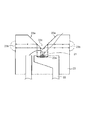
- FIG. 2 is a diagram showing a configuration of a light emitting device described in Patent Document 2.
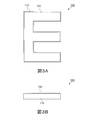
- 3A and 3B are diagrams showing the configuration of the lighting device according to the embodiment.
- FIG. 4 is a plan view of the lighting device with the light diffuser removed.
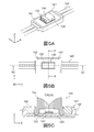
- 5A to 5C are diagrams showing the configuration of the light emitting device shown in FIG. 4 and its surroundings.
- 6A to 6C are views showing the configuration of the light beam control member according to the embodiment.
- 7A and 7B are diagrams showing the configuration of the luminous flux control member according to the embodiment.
- FIG. 8 is a cross-sectional view of the light emitting device and its surroundings in line 8-8 of FIG. 5B.
- FIG. 9 is a cross-sectional view showing the configuration of the light emitting device according to the modified example.
- FIG. 10 is a partially enlarged perspective view showing a modified example of the lighting device.
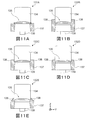
- 11A to 11E are cross-sectional views showing the configuration of the light beam control member to be simulated.
- FIG. 12 is a diagram showing a luminance distribution on a light diffusing plate when a first luminous flux control member having no two walls is used.
- FIG. 3A, 3B and 4 are diagrams showing the configuration of the lighting device 100 according to the embodiment of the present invention.
- FIG. 3A is a plan view of the lighting device 100
- FIG. 3B is a front view
- FIG. 4 is a plan view of the lighting device 100 with the light diffusing plate 150 removed.
- 5A to 5C are diagrams showing the configuration of the light emitting device 130 shown in FIG. 4 and its surroundings.
- 5A is a perspective view of the light emitting device 130 and its surroundings
- FIG. 5B is a plan view
- FIG. 5C is a sectional view taken along line 5C-5C of FIG. 5B.
- the lighting device 100 according to the present embodiment is used, for example, as a channel character type signboard.
- the lighting device 100 includes a housing 110, a plurality of substrates 120 (see FIG. 5C), a plurality of light emitting devices 130, a plurality of cables 140 and a light diffusing plate 150. ..
- the housing 110 is a box-shaped body in which at least a part of one surface is open for accommodating a plurality of substrates 120 and a plurality of light emitting devices 130.
- the housing 110 is composed of a bottom plate, a top plate arranged so as to face the bottom plate, and a plurality of side plates connecting the bottom plate and the top plate.
- the top plate is formed with an opening that serves as a light emitting region. This opening is closed by the light diffusing plate 150.
- the plan view shape of the housing 110 is not particularly limited. In the present embodiment, the plan view shape of the housing 110 is the shape of the alphabet "E".
- the space thickness of the housing 110 is not particularly limited, but is, for example, about 20 to 100 mm.
- the housing 110 is made of, for example, a resin such as polymethyl methacrylate (PMMA) or polycarbonate (PC), or a metal such as stainless steel or aluminum.
- the plurality of substrates 120 are flat plates for arranging the plurality of light emitting devices 130 on the bottom plate of the housing 110 at predetermined intervals (see FIG. 5C).
- a light emitting element 131 and a light beam control member 132 of the light emitting device 130 are fixed to each substrate 120.
- the substrate 120 is arranged on the bottom plate of the housing 110 via a housing 141 described later (see FIG. 5C).
- the wiring of the substrate 120 is electrically connected to the light emitting element 131 of the light emitting device 130 and the cable 140.
- the plurality of light emitting devices 130 are respectively arranged on the bottom plate of the housing 110 via the plurality of substrates 120. As described above, in the present embodiment, each substrate 120 is housed in the housing 141.
- the number of light emitting devices 130 is not particularly limited, and is appropriately set based on the size of the light emitting region (light emitting surface) defined by the opening of the housing 110.
- the plurality of light emitting devices 130 may be arranged at equal intervals or may be arranged at different intervals.
- Each light emitting device 130 has a light emitting element 131 and a luminous flux control member 132. Each light emitting device 130 is arranged on the substrate 120 so that the optical axis LA of the light emitted from the light emitting element 131 is along the normal line with respect to the surface of the substrate 120 (the surface of the bottom plate of the housing 110).
- the light emitting element 131 is a light source of the lighting device 100 (and the light emitting device 130).
- the light emitting element 131 is arranged on the substrate 120 (see FIG. 5C) and is electrically connected to the wiring formed on the substrate 120 or in the substrate 120.
- the light emitting element 131 is, for example, a light emitting diode (LED).
- the color of the emitted light of the light emitting element 131 is not particularly limited.
- the light emitting element 131 is, for example, an SMD type light emitting element having a light emitting unit that emits blue light and a phosphor that converts blue light emitted from the light emitting unit into white light.
- the luminous flux control member 132 controls the light distribution of the light emitted from the light emitting element 131. Specifically, the luminous flux control member 132 makes the traveling direction of the light emitted from the light emitting element 131 substantially perpendicular to the surface direction of the substrate 120, particularly the optical axis LA of the light emitting element 131, and is opposite to each other. Change in two directions.
- the luminous flux control member 132 is arranged on the substrate 120 so that its incident surface 133 faces the light emitting element 131 (see FIG. 5C). In the present embodiment, the luminous flux control member 132 is arranged so that its central axis CA coincides with the optical axis LA of the light emitting element 131.
- the "optical axis LA of the light emitting element 131” means a light beam at the center of a three-dimensional emitted light beam from the light emitting element 131.
- the "central axis CA of the luminous flux control member 132” means, for example, a axis of symmetry that is twice symmetrical.
- the optical axis LA of the light emitting element 131 passes through the light emitting center of the light emitting element 131 and the axis parallel to the optical axis LA of the light emitting element 131 is the Z axis and the plane is perpendicular to the Z axis.
- the two axes that pass through and are orthogonal to each other are called the X-axis and the Y-axis.
- the X-axis is along the directions in which the two emission surfaces 136 of the luminous flux control member 132 face each other (the first direction and the second direction described later).
- the Y-axis is along the direction in which the groove 135 of the light beam control member 132 extends (the third direction and the fourth direction described later).
- the material of the light beam control member 132 is not particularly limited as long as it can pass light of a desired wavelength.
- the material of the light beam control member 132 is a light-transmitting resin such as polymethyl methacrylate (PMMA), polycarbonate (PC), epoxy resin (EP), or glass.
- PMMA polymethyl methacrylate
- PC polycarbonate
- EP epoxy resin
- glass glass
- the cable 140 electrically connects a plurality of adjacent boards 120 to each other.
- the connection between the substrate 120 and the cable 140 is reinforced with a housing 141 and a caulking material 142 (see FIG. 5C).
- the housing 141 is filled with a caulking material 142.
- the caulking material 142 functions as a covering material that fills the gap between the substrate 120 and the luminous flux control member 132 at the peripheral edge portion on the back side of the luminous flux control member 132.
- a light-transmitting resin as the coking material 142, it is possible to prevent a decrease in the emission efficiency from the light emitting device 130.
- materials constituting the housing 141 include resins such as polycarbonate (PC).
- materials constituting the caulking material 142 include urethane resin, silicone resin, and epoxy resin.
- the plurality of light emitting devices 130 can be freely arranged according to the shape of the housing 110. Further, in each module (light emitting device 130), the gap between the substrate 120 and the light beam control member 132 is filled with a coking material 142 (coating material) to impart waterproofness to each module (light emitting device 130). Can be done.
- the light diffusing plate 150 is arranged so as to close the opening of the housing 110 (see FIGS. 3A and 3B).
- the light diffusing plate 150 is a plate-shaped member having light transmissivity and light diffusing property, and transmits the emitted light from the emitting surface 136 (see FIGS. 6A to 6C) of the luminous flux control member 132 while diffusing it.
- the light diffusing plate 150 can function as a light emitting surface of the lighting device 100.
- the material of the light diffusing plate 150 is not particularly limited as long as it can transmit the emitted light from the emitting surface 136 of the luminous flux control member 132 while diffusing it.
- the material of the light diffusing plate 150 is a light transmitting resin such as polymethyl methacrylate (PMMA), polycarbonate (PC), polystyrene (PS), and styrene / methyl methacrylate copolymer resin (MS).
- PMMA polymethyl methacrylate
- PC polycarbonate
- PS polystyrene
- MS styrene / methyl methacrylate copolymer resin
- fine irregularities are formed on the surface of the light diffusing plate 150, or light diffusing elements such as beads are dispersed inside the light diffusing plate 150.
- the light emitted from each light emitting element 131 is substantially relative to the optical axis LA of the light emitting element 131 so as to illuminate a wide range of the light diffusing plate 150 by the luminous flux control member 132.
- the light is converted into light emitted in two directions (directions along the X axis in FIGS. 5A to 5C) that are vertically opposite to each other.
- the light emitted from each light beam control member 132 is further diffused by the light diffusing plate 150 and emitted to the outside.
- FIG. 6A to 6C, 7A and 7B are diagrams showing the configuration of the luminous flux control member 132.
- 6A is a plan view of the luminous flux control member 132
- FIG. 6B is a bottom view
- FIG. 6C is a cross-sectional view taken along the line 6C-6C of FIG. 6A.
- FIG. 7A is a right side view of the light beam control member 132
- FIG. 7B is a cross-sectional view taken along the line 7B-7B of FIG. 6A.
- the luminous flux control member 132 controls the light distribution of the light emitted from the light emitting element 131.
- the luminous flux control member 132 includes an incident surface 133, two reflecting surfaces 134, a groove 135, two emitting surfaces 136, a collar 137, two walls 138, and It has two legs 139.
- the side on which the incident surface of the light beam control member 132 is formed (the side of the light emitting element 131) is referred to as the back side, and the side on which the reflection surface 134 is formed is referred to as the front side.
- the incident surface 133 is incident with a part of the light emitted from the light emitting element 131.
- the incident surface 133 is an inner surface of a recess formed in the central portion on the back side of the luminous flux control member 132.
- the shape of the inner surface of the concave portion is not particularly limited, and may be a surface including an edge, or a curved surface having no edge, such as a hemispherical shape or a semi-elliptical shape.
- the inner surface shape of the recess is a surface including an edge.
- the incident surface 133 (inner surface of the recess) has at least a first inner top surface 133a and two inner surface 133b, and further has two second inner top surfaces 133c between them (FIG. FIG. See 6C).
- the two second inner top surfaces 133c are arranged so as to sandwich the first inner top surface 133a in the direction in which the two exit surfaces 136 face each other (direction along the X axis).
- the first inner top surface 133a is a surface arranged in the central portion of the recess so as to intersect the optical axis LA of the light emitting element 131.
- the first inner top surface 133a is the optical axis of the light emitting element 131 from the viewpoint of preventing light emitted at a small angle with respect to the optical axis LA of the light emitting element 131 from traveling to the boundary between the two reflecting surfaces 134. It may be formed so that the height of the light emitting element 131 from the light emitting surface increases as it approaches LA.
- the two reflecting surfaces 134 are arranged on the front side of the light beam control member 132, that is, on the side opposite to the light emitting element 131 (on the light diffusing plate 150 side) with the incident surface 133 in between. Further, the two reflecting surfaces 134 have two directions (first direction and second direction) in which a part of the light incident from the incident surface 133 is substantially perpendicular to the optical axis LA of the light emitting element 131 and opposite to each other. Reflect in the direction). The first direction and the second direction are directions along the X axis.
- the two reflecting surfaces 134 are from the optical axis LA of the light emitting element 131 to the light beam control member 132 with the optical axis LA of the light emitting element 131 as a boundary. Each is formed so that the height from the substrate 120 increases toward the end (exit surface 136). Further, in the present embodiment, in this cross section, the inclination of the tangential lines of the two reflecting surfaces 134 gradually decreases from the optical axis LA of the light emitting element 131 toward the end portion (emission surface 136) of the luminous flux control member 132. Each is formed so as to be.
- the two reflecting surfaces 134 are formed so that the height from the substrate 120 increases toward the end portion (exit surface 136) of the luminous flux control member 132 from the optical axis LA of the light emitting element 131. There is. Therefore, a substantially V-shaped groove 135 is formed between the two reflecting surfaces 134.
- the groove 135 extends in the third and fourth directions which are substantially perpendicular to the directions (first and second directions) along the optical axes LA and X of the light emitting element 131 and which are opposite to each other.
- the third and fourth directions are directions along the Y axis. That is, the groove 135 extends in the direction along the Y axis.
- the groove 135 is open to the outside not only on the front side but also in the third direction and the fourth direction.
- the two exit surfaces 136 are arranged so as to face each other with the two reflection surfaces 134 and the groove 135 interposed therebetween.
- the two exit surfaces 136 are incident on the incident surface 133 (particularly the two inner surface 133b) and directly reach the exit surface 136, and are incident on the incident surface 133 (particularly the first inner top surface 133a).
- the light reflected by the reflecting surface 134 is emitted to the outside.
- the exit surface 136 may be a flat surface or a curved surface.
- the exit surface 136 is a curved surface including a plurality of ridges extending in a direction substantially parallel to the optical axis LA (Z axis) of the light emitting element.
- the shape of each ridge is substantially triangular, and a plurality of ridges are arranged without gaps. Further, the ridgeline of each ridge and the valley line formed between the two ridges adjacent to each other are R-chamfered. Therefore, the shape of the horizontal cross section (cross section parallel to the X-axis and the Y-axis) of the exit surface 136 is a wavy curve.
- the collar 137 is located between the bottom surface of the luminous flux control member 132 (the surface in contact with the substrate 120), the two exit surfaces 136, and the bottom surface of the luminous flux control member 132, and is perpendicular to the central axis CA of the luminous flux control member 132. It protrudes in the direction.
- the shape of the collar 137 is not particularly limited, and is substantially rectangular in the present embodiment. The provision of the collar 137 facilitates the handling and alignment of the luminous flux control member 132.
- the coking material 142 (coating material) is placed in the recess on the back side of the light beam control member 132 (the recess that constitutes the incident surface 133). It can also prevent inflow.
- the thickness of the collar 137 is not particularly limited, and can be determined in consideration of the required area of the two exit surfaces 136, the moldability of the collar 137, and the like.
- the two walls 138 are configured to extend from the bottom of the groove 135 to a predetermined height and close the openings in the third direction and the fourth direction (direction along the Y axis) of the groove 135, respectively.
- the two walls 138 are plate-shaped members arranged on the brim 137 so as to project from the brim 137 toward the front side. The two walls 138 prevent the coking material 142 (coating material) from entering the groove 135.
- FIG. 8 is a cross-sectional view of the light emitting device 130 and its periphery in line 8-8 of FIG. 5B.
- the two walls 138 are configured to close a portion of the groove 135 below the openings in the third and fourth directions, respectively. Therefore, even if the coking material 142 before solidification is provided on the peripheral edge of the light beam control member 132 in order to fill the gap between the substrate 120 and the light beam control member 132, the coking material 142 is the groove 135 of the light beam control member 132. Do not infiltrate. Therefore, the light distribution characteristic of the light flux control member 132 does not change due to the caulking material 142 adhering to the reflecting surface 134.
- the height of the two walls 138 (the length in the direction along the Z axis) is particularly high as long as the above functions can be appropriately exerted and the change in the light distribution characteristics of the luminous flux control member 132 is within an allowable range. Not limited.
- the thicknesses of the two walls 138 can also appropriately exert the above functions, and the light distribution characteristics of the light beam control member 132 are changed. Is not particularly limited as long as is within the permissible range. From the viewpoint of suppressing changes in the light distribution characteristics of the light beam control member 132, it is preferable that the thicknesses of the two walls 138 become smaller toward the front side. Further, it is preferable that each of the two walls 138 has an inclined surface that approaches the groove 135 toward the front side. By doing so, it is possible to suppress a change in the light distribution characteristics of the luminous flux control member 132 due to the provision of the wall 138.
- the two leg portions 139 are substantially columnar convex portions protruding from the bottom surface of the light beam control member 132 to the back side.
- the two legs 139 are fitted into substantially cylindrical recesses (positioning holes) formed in the substrate 120 (see FIG. 5C). By doing so, the luminous flux control member 132 can be easily positioned at an appropriate position with respect to the light emitting element 131.
- the number of legs 139 is not particularly limited.
- the light beam control member 132 since the light beam control member 132 has two walls 138 that close a part of the openings in the third direction and the fourth direction of the groove 135, it is a substrate. Even if the coking material 142 (covering material) before solidification is provided on the peripheral edge of the light beam control member 132 in order to fill the gap between the 120 and the light beam control member 132, the coking material 142 is the groove of the light beam control member 132. Does not penetrate 135 (see FIG. 8). Therefore, in the lighting device 100 according to the present embodiment, the light distribution characteristic of the light beam control member 132 is unlikely to change due to the coking material 142 adhering to the reflecting surface 134.
- the present invention is not limited to this.
- the plurality of light emitting devices 130 may be arranged on one substrate 120. In this case, the cable 140 is unnecessary.
- the light emitting device 130 is modularized by accommodating the substrate 120, the light emitting element 131, and the light beam control member 132 in the housing 141, and then filling the housing 141 with the coking material 142 (coating material).
- the present invention is not limited to this.
- the light emitting device 130 may be modularized by coating the periphery of the substrate 120 on which the light emitting element 131 and the luminous flux control member 132 are mounted with the resin 143 by insert molding or the like.
- the resin 143 functions as a coating material that fills the gap between the substrate 120 and the light beam control member 132 at the peripheral edge on the back side of the light beam control member 132.
- the two walls 138 prevent the liquid resin 143 (coating material) in the molten state or before being cured from entering the groove 135.
- the resin 143 include polybutylene terephthalate (PBT) and the like.
- the lighting device 100 in which the housing 110 includes a bottom plate, a side plate, and a top plate (at least partially provided with an opening) is described. Not limited to.
- the top plate and side plates of the housing 110 may be omitted, and the bottom plate of the housing 110 may be covered with the light diffusing plate 150.
- the lighting device 100 which is a channel character type signboard has been described, but the present invention is not limited to this.
- the lighting device according to the present invention may be line lighting, general lighting, or the like.
- FIGS. 11A to 11E are cross-sectional views showing the configuration of the luminous flux control member to be simulated. These figures show a cross section of line 7B-7B of FIG. 6A, similar to FIG. 7B.
- the first luminous flux control member 132A shown in FIG. 1A does not have two walls 138. Assuming that the point indicated by the double circle (the end of the valley line of the groove 135) in FIG. 11A is the reference point, the length (W) of the upper surface of the collar 137 in the Y-axis direction is 0.85 mm, and the length (W) of the collar 137 is The position (H) of the upper surface in the Z-axis direction is ⁇ 0.05 mm.
- the second light beam control member 132B shown in FIG. 11B has two walls 138 having a constant thickness.
- the length (W) of the upper surface of the wall 138 in the Y-axis direction is 0.85 mm, and the position (H) of the upper surface of the wall 138 in the Z-axis direction is 1.00 mm.
- the third luminous flux control member 132C shown in FIG. 11C also has two walls 138 having a constant thickness.
- the length (W) of the upper surface of the wall 138 in the Y-axis direction is 0.85 mm, and the position (H) of the upper surface of the wall 138 in the Z-axis direction is 0.50 mm.
- the fourth light beam control member 132D shown in FIG. 11D has two walls 138 that become thinner toward the front side.
- the length (W) of the upper surface of the wall 138 in the Y-axis direction is 0.60 mm
- the position (H) of the upper surface of the wall 138 in the Z-axis direction is 0.50 mm.
- the fifth light beam control member 132E shown in FIG. 11E also has two walls 138 that become thinner toward the front side.
- the length (W) of the upper surface of the wall 138 in the Y-axis direction is 0.30 mm
- the position (H) of the upper surface of the wall 138 in the Z-axis direction is 0.50 mm.
- FIG. 12 is a diagram showing the brightness distribution on the light diffusing plate 150 when the first luminous flux control member 132A having no two walls 138 is used.
- This figure is originally a figure in which the central part is red and the peripheral part is blue.
- the first luminous flux control member 132A having no two walls 138 is used, the brightness distribution becomes elliptical.
- the value obtained by dividing the half-value width of the brightness distribution on the X-axis (long axis) by the half-value width of the Y-axis (minor axis) -shaped brightness distribution is defined as the "elliptical ratio"
- the first light beam control member 132A The ellipticity of the brightness distribution when is used is 1.37.
- Table 1 shows the ellipticity of the brightness distribution when other light beam control members are used.
- the numerical values in parentheses indicate the rate of change (%) of the ellipticity when the ellipticity of the luminance distribution when the first luminous flux control member 132A is used is used as a reference.
- the luminous flux control member 132 is provided with two walls 138, the light passing through the wall 138 can easily reach the area surrounded by the square in FIG. This region is located substantially directly above the light emitting device 130 and is close to the light emitting device 130. Therefore, when the amount of light reaching this region increases, uneven brightness tends to occur. Therefore, when the luminous flux in this region when the first luminous flux control member 132A is used is 1, the luminous flux ratio in this region when another luminous flux control member is used is calculated as shown in Table 1. ..
- the thickness of the two walls 138 is reduced toward the front side, which is caused by the two walls 138. It can be seen that changes in the light distribution characteristics of the luminous flux control member 132 can be suppressed.
- the light beam control member, light emitting device and lighting device according to the present invention can be applied to, for example, signboards (particularly channel character type signboards), line lighting, general lighting and the like.
- Lighting device 11 Housing 12
- Light emitting device 13 Light diffuser plate 14, 15 Prism sheet 16
- External protective cover 17 Light beam control member 21
- Light emitting element 22 Base 22a Reflection cup 23
- Light beam control member 23a Reflection surface 23b Exit surface 23c Groove 100
- Lighting device 110 Housing 120 Board 130
- Light emitting device 131 Light emitting element 132
- Light beam control member 133 Incident surface 133a Inner top surface (first inner top surface) 133b
- Inner side surface 133c Second inner top surface 134
- Reflective surface 135 Groove 136 Exit surface 137 Bound 138 Wall 139
- Leg 140 Cable 141 Housing 142
- Caulking material (covering material) 143 resin (coating material)
- Optical diffusing plate CA Central axis of luminous flux control member LA
Landscapes
- Engineering & Computer Science (AREA)
- General Engineering & Computer Science (AREA)
- Physics & Mathematics (AREA)
- General Physics & Mathematics (AREA)
- Theoretical Computer Science (AREA)
- Optics & Photonics (AREA)
- Planar Illumination Modules (AREA)
- Optical Elements Other Than Lenses (AREA)
- Illuminated Signs And Luminous Advertising (AREA)
- Led Device Packages (AREA)
Abstract
本発明は、周囲にコーキング材を提供しても配光特性が変わりにくい光束制御部材に関する。光束制御部材は、裏側に配置された入射面と、表側に互いに対向して配置された2つの反射面と、2つの反射面により構成される溝と、2つの出射面と、溝の開口部を塞ぐ2つの壁と、を有する。2つの壁の溝の延在方向における厚みは、表側に向かうにつれて小さくなる。
Description
本発明は、光束制御部材、発光装置および照明装置に関する。
チャンネル文字型看板などの照明装置の光源として、LEDなどの発光素子を有する発光装置が使用されている(例えば特許文献1)。
図1は、チャンネル文字型看板として用いられる特許文献1に記載の照明装置を示す斜視図である。図1に示されるように、照明装置10は、文字型の筐体11と、筐体11の内部に配置された複数の発光装置12(特許文献1ではLEDおよび光ダイバータ)と、筐体11の開口部を塞ぐように配置された光拡散板13(特許文献1ではディフューザ)と、プリズムシート14、15と、外部保護カバー16とを有している。発光装置12は、発光素子(特許文献1ではLED)と、光束制御部材17(特許文献1では光ダイバータ)とを有している。光束制御部材17は、発光素子(不図示)から出射された光を全方向に等方的に拡げる。
このようなチャンネル文字型看板では、低消費電力化の観点などから、発光素子の数を少なくすることが望まれている。すなわち、発光素子の数を少なくしても、光拡散板の全体に光をある程度均一に到達させることが望まれている。そのため、特許文献1のように、発光素子から出射される光を全方向に等方的に拡げる光束制御部材(等方的な配光特性を有する光束制御部材)ではなく、特定の方向に異方的に拡げる光束制御部材(異方的な配光特性を有する光束制御部材)を用いることが検討されている。具体的には、発光素子から出射される光を水平方向で互いに反対向きである2つの方向に反射させることにより、配光特性に異方性を持たせた(楕円配光を示す)光束制御部材を用いることが検討されている。
配光特性に異方性を持たせた発光装置として、例えば特許文献2には、図2に示されるように、発光素子21と、発光素子21から出射された光を上方へ反射させる反射カップ22aを有する基台22と、発光素子21および反射カップ22aを封止する光束制御部材23(特許文献2では透光性樹脂)とを有する発光装置が開示されている。光束制御部材23は、発光素子21から出射された光や反射カップ22aで反射された光を反射する2つの反射面23aと、反射面23aで反射された光を外部へ出射する2つの出射面23b(特許文献2では側面)とを有する。光束制御部材23では、2つの反射面23aにより溝23cが形成されている。
このような発光装置では、発光素子21の上面から出射された光は、光束制御部材23の反射面23aに直接到達し、発光素子21の側面から出射された光は、反射カップ22aで反射された後、光束制御部材23の2つの反射面23aに到達する。そして、2つの反射面23aに到達した光は、反射面23aで水平方向で互いに反対向きの方向に反射され、2つの出射面23bから外部へ出射される。
チャンネル文字型看板が屋外に配置される場合、チャンネル文字型看板内の発光装置には防水性が要求される。発光装置に防水性を付与する手段としては、光束制御部材の周縁部において、発光素子が配置されている基板と光束制御部材との間の隙間をコーキング材などの被覆材で埋めることが考えられる。しかしながら、特許文献2に記載されているような、2つの反射面の間に溝が形成されている光束制御部材を用いる場合、光束制御部材の周縁部に被覆材を提供すると、被覆材が溝に流れ込んでしまうことがある。このように被覆材が溝に流れ込んでしまうと、2つの反射面が適切に機能することができなくなり、光束制御部材の配光特性が顕著に変化してしまう。
そこで、本発明の目的は、周囲に被覆材を提供しても配光特性が変わりにくい光束制御部材を提供することである。また、本発明の別の目的は、この光束制御部材を有する発光装置および照明装置を提供することである。
本発明に係る光束制御部材は、発光素子から出射された光の配光を制御するための光束制御部材であって、裏側に配置された凹部の内面であって、発光素子から出射された光を入射する入射面と、表側に互いに対向して配置され、前記入射面で入射した光の一部を、前記発光素子の光軸と略垂直であり、かつ互いに反対向きである第1方向および第2方向にそれぞれ反射させる2つの反射面と、前記2つの反射面により構成される、前記光軸、前記第1方向および前記第2方向に略垂直であり、かつ互いに反対向きである第3方向および第4方向に延在する溝と、前記2つの反射面および前記溝を挟んで互いに対向して配置され、前記2つの反射面で反射された光をそれぞれ外部に出射させる2つの出射面と、前記溝の底部から所定の高さまでに亘り、前記溝の前記第3方向および前記第4方向の開口部をそれぞれ塞ぐ2つの壁と、を有し、前記2つの壁の前記第3方向および前記第4方向における厚みは、それぞれ、表側に向かうにつれて小さくなる。
本発明に係る光束制御部材は、発光素子と、前記入射面が前記発光素子と対向するように配置された、本発明に係る光束制御部材と、を有する。
本発明に係る照明装置は、本発明に係る発光装置と、前記発光装置から出射された光を拡散させつつ透過させる光拡散板と、を有する。
本発明によれば、周囲に被覆材を提供しても配光特性が変わりにくい光束制御部材を提供することができる。また、本発明によれば、この光束制御部材を有する発光装置および照明装置を提供することもできる。
以下、本発明の実施の形態について、図面を参照して詳細に説明する。
(照明装置の構成)
図3A、図3Bおよび図4は、本発明の一実施の形態に係る照明装置100の構成を示す図である。図3Aは、照明装置100の平面図であり、図3Bは、正面図である。図4は、光拡散板150を外した状態の照明装置100の平面図である。図5A~Cは、図4に示される発光装置130およびその周辺の構成を示す図である。図5Aは、発光装置130およびその周辺の斜視図であり、図5Bは、平面図であり、図5Cは、図5Bの5C-5C線の断面図である。本実施の形態に係る照明装置100は、例えばチャンネル文字型看板として用いられる。
図3A、図3Bおよび図4は、本発明の一実施の形態に係る照明装置100の構成を示す図である。図3Aは、照明装置100の平面図であり、図3Bは、正面図である。図4は、光拡散板150を外した状態の照明装置100の平面図である。図5A~Cは、図4に示される発光装置130およびその周辺の構成を示す図である。図5Aは、発光装置130およびその周辺の斜視図であり、図5Bは、平面図であり、図5Cは、図5Bの5C-5C線の断面図である。本実施の形態に係る照明装置100は、例えばチャンネル文字型看板として用いられる。
図3A、図3Bおよび図4に示されるように、照明装置100は、筐体110、複数の基板120(図5C参照)、複数の発光装置130、複数のケーブル140および光拡散板150を有する。
筐体110は、その内部に複数の基板120および複数の発光装置130を収容するための、1つの面の少なくとも一部が開放された箱状体である。本実施の形態では、筐体110は、底板と、底板に対向するように配置された天板と、底板と天板とを繋ぐ複数の側板とで構成されている。天板には、発光領域となる開口部が形成されている。この開口部は、光拡散板150により塞がれる。筐体110の平面視形状は、特に限定されない。本実施の形態では、筐体110の平面視形状は、アルファベットの「E」の形である。
筐体110の空間厚さ(底板と光拡散板150との間隔)は、特に限定されないが、例えば20~100mm程度である。筐体110は、例えば、ポリメタクリル酸メチル(PMMA)やポリカーボネート(PC)などの樹脂や、ステンレス鋼やアルミニウムなどの金属などから構成される。
複数の基板120は、複数の発光装置130を、筐体110の底板上に所定の間隔で配置するための平板である(図5C参照)。各基板120には、発光装置130の発光素子131および光束制御部材132が固定されている。本実施の形態では、基板120は、筐体110の底板上に、後述するハウジング141を介して配置されている(図5C参照)。基板120の配線は、発光装置130の発光素子131およびケーブル140に電気的に接続されている。
複数の発光装置130は、筐体110の底板上に、複数の基板120を介してそれぞれ配置されている。前述のとおり、本実施の形態では、各基板120は、ハウジング141内に収容されている。発光装置130の数は、特に限定されず、筐体110の開口部により規定される発光領域(発光面)の大きさに基づいて適宜設定される。複数の発光装置130は、等間隔に配置されてもよいし、異なる間隔で配置されていてもよい。
各発光装置130は、発光素子131および光束制御部材132を有する。各発光装置130は、発光素子131から出射される光の光軸LAが基板120の表面(筐体110の底板の表面)に対する法線に沿うように基板120上に配置されている。
発光素子131は、照明装置100(および発光装置130)の光源である。発光素子131は、基板120上に配置されており(図5C参照)、基板120上または基板120内に形成された配線と電気的に接続されている。発光素子131は、例えば発光ダイオード(LED)である。発光素子131の出射光の色は、特に限定されない。発光素子131は、例えば、青色光を発する発光部と、発光部から出射される青色光を白色光に変換する蛍光体とを有するSMDタイプの発光素子である。
光束制御部材132は、発光素子131から出射された光の配光を制御する。具体的には、光束制御部材132は、発光素子131から出射された光の進行方向を、基板120の面方向、特に発光素子131の光軸LAに対して略垂直であり、かつ互いに反対向きである2つの方向に変える。光束制御部材132は、その入射面133が発光素子131と対向するように、基板120上に配置されている(図5C参照)。本実施の形態では、光束制御部材132は、その中心軸CAが発光素子131の光軸LAに一致するように配置されている。本明細書において、「発光素子131の光軸LA」とは、発光素子131からの立体的な出射光束の中心の光線を意味する。また、「光束制御部材132の中心軸CA」とは、例えば2回対称の対称軸をいう。
以下、各発光装置130において、発光素子131の発光中心を通り、かつ発光素子131の光軸LAに平行な軸をZ軸、Z軸に対して垂直な平面において、発光素子131の光軸LAを通り、かつ互いに直交する2つの軸をX軸およびY軸という。X軸は、光束制御部材132の2つの出射面136が対向する方向(後述する第1方向および第2方向)に沿っている。一方、Y軸は、光束制御部材132の溝135が延在する方向(後述する第3方向および第4方向)に沿っている。
光束制御部材132の材料は、所望の波長の光を通過させうるものであれば特に限定されない。たとえば、光束制御部材132の材料は、ポリメタクリル酸メチル(PMMA)やポリカーボネート(PC)、エポキシ樹脂(EP)などの光透過性樹脂、またはガラスである。光束制御部材132については、別途詳細に説明する。
ケーブル140は、隣り合う複数の基板120同士を電気的に接続している。基板120とケーブル140の接続部は、ハウジング141およびコーキング材142で補強されている(図5C参照)。また、ハウジング141内には、コーキング材142が充填されている。コーキング材142は、光束制御部材132の裏側の周縁部において、基板120と光束制御部材132との間の隙間を埋める被覆材として機能する。また、コーキング材142として、光透過性の樹脂を用いることで、発光装置130からの出射効率の低下を防ぐことができる。ハウジング141を構成する材料の例には、ポリカーボネート(PC)などの樹脂が含まれる。コーキング材142を構成する材料の例には、ウレタン樹脂、シリコーン樹脂、エポキシ樹脂が含まれる。
このように、複数の発光装置130をモジュール化し、これらをケーブル140を介して電気的に接続することで、複数の発光装置130を筐体110の形状に合わせて自在に配置することができる。また、各モジュール(発光装置130)において、基板120と光束制御部材132との間の隙間をコーキング材142(被覆材)で埋めることで、各モジュール(発光装置130)に防水性を付与することができる。
光拡散板150は、筐体110の開口部を塞ぐように配置されている(図3Aおよび図3B参照)。光拡散板150は、光透過性および光拡散性を有する板状の部材であり、光束制御部材132の出射面136(図6A~C参照)からの出射光を拡散させつつ透過させる。光拡散板150は、照明装置100の発光面として機能しうる。
光拡散板150の材料は、光束制御部材132の出射面136からの出射光を拡散させつつ透過させうるものであれば特に限定されない。たとえば、光拡散板150の材料は、ポリメタクリル酸メチル(PMMA)やポリカーボネート(PC)、ポリスチレン(PS)、スチレン・メチルメタクリレート共重合樹脂(MS)などの光透過性樹脂である。光拡散性を付与するため、光拡散板150の表面に微細な凹凸が形成されているか、または光拡散板150の内部にビーズなどの光拡散子が分散している。
本実施の形態に係る照明装置100では、各発光素子131から出射された光は、光束制御部材132により光拡散板150の広範囲を照らすように、特に発光素子131の光軸LAに対して略垂直方向に、かつ互いに反対向きである2つの方向(図5A~CにおけるX軸に沿う方向)へ向かう光に変えられて出射される。各光束制御部材132から出射された光は、さらに光拡散板150により拡散されて、外部に出射される。
(光束制御部材の構成)
図6A~C、図7Aおよび図7Bは、光束制御部材132の構成を示す図である。図6Aは、光束制御部材132の平面図であり、図6Bは、底面図であり、図6Cは、図6Aの6C-6C線の断面図である。図7Aは、光束制御部材132の右側面図であり、図7Bは、図6Aの7B-7B線の断面図である。
図6A~C、図7Aおよび図7Bは、光束制御部材132の構成を示す図である。図6Aは、光束制御部材132の平面図であり、図6Bは、底面図であり、図6Cは、図6Aの6C-6C線の断面図である。図7Aは、光束制御部材132の右側面図であり、図7Bは、図6Aの7B-7B線の断面図である。
光束制御部材132は、発光素子131から出射された光の配光を制御する。図6A~C、図7Aおよび図7Bに示されるように、光束制御部材132は、入射面133、2つの反射面134、溝135、2つの出射面136、鍔137、2つの壁138、および2つの脚部139を有する。以下、光束制御部材132の入射面が形成されている側(発光素子131側)を裏側、反射面134が形成されている側を表側という。
入射面133は、発光素子131から出射された光の一部を入射させる。入射面133は、光束制御部材132の裏側の中央部に形成された凹部の内面である。凹部の内面形状は、特に限定されず、エッジを含む面であってもよいし、半球状や半楕円体状などのように、エッジを含まない曲面であってもよい。本実施の形態では、凹部の内面形状は、エッジを含む面である。
具体的には、入射面133(凹部の内面)は、少なくとも第1内天面133aおよび2つの内側面133bを有し、それらの間に、2つの第2内天面133cをさらに有する(図6C参照)。2つの第2内天面133cは、2つの出射面136が対向する方向(X軸に沿う方向)において、第1内天面133aを挟むように配置されている。
第1内天面133aは、発光素子131の光軸LAと交わるように、凹部の中央部に配置された面である。第1内天面133aは、発光素子131の光軸LAに対して小さい角度で出射される光を、2つの反射面134の境界部に進行させないようにする観点から、発光素子131の光軸LAに近づくにつれて、発光素子131の発光面からの高さが高くなるように形成されていてもよい。
2つの反射面134は、光束制御部材132の表側、すなわち入射面133を挟んで発光素子131と反対側(光拡散板150側)に配置されている。また、2つの反射面134は、入射面133から入射した光の一部を、発光素子131の光軸LAと略垂直であり、かつ互いに反対向きである2つの方向(第1方向および第2方向)に反射させる。第1方向および第2方向は、X軸に沿う方向である。発光素子131の光軸LAを含み、かつX軸と平行な断面において、2つの反射面134は、発光素子131の光軸LAを境界として、発光素子131の光軸LAから光束制御部材132の端部(出射面136)に向かうにつれて、基板120からの高さが高くなるようにそれぞれ形成されている。また、本実施の形態では、2つの反射面134は、この断面において、発光素子131の光軸LAから光束制御部材132の端部(出射面136)に向かうにつれて、接線の傾きが徐々に小さくなるようにそれぞれ形成されている。
上記のとおり、2つの反射面134は、発光素子131の光軸LAから光束制御部材132の端部(出射面136)に向かうにつれて、基板120からの高さが高くなるようにそれぞれ形成されている。したがって、2つの反射面134の間には、略V字状の溝135が形成される。溝135は、発光素子131の光軸LA、X軸に沿う方向(第1方向および第2方向)に略垂直であり、かつ互いに反対向きである第3方向および第4方向に延在する。第3方向および第4方向は、Y軸に沿う方向である。すなわち、溝135は、Y軸に沿う方向に延在する。溝135は、表側だけでなく、第3方向および第4方向においても外部に開口している。
2つの出射面136は、2つの反射面134および溝135を挟んで互いに対向して配置されている。2つの出射面136は、入射面133(特に2つの内側面133b)で入射し、出射面136に直接到達した光、および入射面133(特に第1内天面133a)で入射し、2つの反射面134で反射された光を外部にそれぞれ出射させる。
出射面136は、平面であってもよいし、曲面であってもよい。本実施の形態では、出射面136は、発光素子の光軸LA(Z軸)と略平行な方向に延在する複数の凸条を含む曲面である。各凸条の形状は、略三角柱状であり、複数の凸条が隙間なく配置されている。また、各凸条の稜線と、互いに隣接する2つの凸条の間に形成される谷線とは、いずれもR面取りされている。したがって、出射面136の水平断面(X軸およびY軸に平行な断面)の形状は、波状の曲線である。出射面136をこのような曲面とすることで、発光装置130から出射される光の輝度ムラおよび色ムラをより抑制することができる。
鍔137は、光束制御部材132の底面(基板120と接する面)と2つの出射面136と光束制御部材132の底面との間に位置し、光束制御部材132の中心軸CAに対して垂直な方向に突出している。鍔137の形状は、特に限定されず、本実施の形態では略長方形である。鍔137を設けることで、光束制御部材132の取り扱いおよび位置合わせが容易になる。また、鍔137を光束制御部材132の全周に基板120と接するように設けることで、コーキング材142(被覆材)が光束制御部材132の裏側の凹部(入射面133を構成する凹部)内に流入するのを防止することもできる。鍔137の厚みは、特に制限されず、2つの出射面136の必要面積や鍔137の成形性などを考慮して決定されうる。
2つの壁138は、溝135の底部から所定の高さまでに亘り、溝135の第3方向および第4方向(Y軸に沿う方向)の開口部をそれぞれ塞ぐように構成されている。本実施の形態では、2つの壁138は、鍔137から表側に向かって突出するように鍔137の上に配置されている、板状の部材である。2つの壁138は、コーキング材142(被覆材)が溝135内に浸入することを防止する。
図8は、図5Bの8-8線における発光装置130およびその周辺の断面図である。図8に示されるように、2つの壁138は、溝135の第3方向および第4方向の開口部の下側の一部をそれぞれ塞ぐように構成されている。したがって、基板120と光束制御部材132との間の隙間を埋めるために光束制御部材132の周縁部に固化する前のコーキング材142を提供したとしても、コーキング材142は光束制御部材132の溝135に浸入しない。したがって、コーキング材142が反射面134に付着することなどによる光束制御部材132の配光特性の変化も生じない。
2つの壁138の高さ(Z軸に沿う方向の長さ)は、上記の機能を適切に発揮することができ、かつ光束制御部材132の配光特性の変化が許容範囲内であれば特に限定されない。
2つの壁138の厚み(Y軸に沿う方向(第3方向および第4方向)の長さ)も、上記の機能を適切に発揮することができ、かつ光束制御部材132の配光特性の変化が許容範囲内であれば特に限定されない。光束制御部材132の配光特性の変化を抑制する観点からは、2つの壁138の厚みは、それぞれ表側に向かうにつれて小さくなることが好ましい。また、2つの壁138は、それぞれ、表側に向かうにつれて溝135に近づく傾斜面を有することが好ましい。このようにすることで、壁138を設けることに起因する光束制御部材132の配光特性の変化を抑制することができる。
2つの脚部139は、光束制御部材132の底面から裏側に突出している略円柱状の凸部である。2つの脚部139は、基板120に形成された略円柱状の凹部(位置決め穴)に嵌め込まれる(図5C参照)。このようにすることで、発光素子131に対して適切な位置に光束制御部材132を容易に位置決めすることができる。なお、脚部139の数は、特に限定されない。
(効果)
以上のように、本実施の形態に係る照明装置100では、光束制御部材132が溝135の第3方向および第4方向の開口部一部を塞ぐ2つの壁138を有しているため、基板120と光束制御部材132との間の隙間を埋めるために光束制御部材132の周縁部に固化する前のコーキング材142(被覆材)を提供したとしても、コーキング材142が光束制御部材132の溝135に浸入しない(図8参照)。したがって、本実施の形態に係る照明装置100では、コーキング材142が反射面134に付着することなどによる光束制御部材132の配光特性の変化が生じにくい。
以上のように、本実施の形態に係る照明装置100では、光束制御部材132が溝135の第3方向および第4方向の開口部一部を塞ぐ2つの壁138を有しているため、基板120と光束制御部材132との間の隙間を埋めるために光束制御部材132の周縁部に固化する前のコーキング材142(被覆材)を提供したとしても、コーキング材142が光束制御部材132の溝135に浸入しない(図8参照)。したがって、本実施の形態に係る照明装置100では、コーキング材142が反射面134に付着することなどによる光束制御部材132の配光特性の変化が生じにくい。
なお、上記実施の形態では、発光装置130と同数の基板120を有する照明装置100について説明したが、本発明はこれに限定されない。たとえば、複数の発光装置130は、1つの基板120上に配置されていてもよい。この場合、ケーブル140は不要である。
また、上記実施の形態では、ハウジング141内に基板120、発光素子131および光束制御部材132を収容した上で、ハウジング141内にコーキング材142(被覆材)を充填することで発光装置130をモジュール化する例について説明したが、本発明はこれに限定されない。たとえば、図9に示されるように、発光素子131および光束制御部材132が実装された基板120の周囲を、インサート成形などにより樹脂143で被覆することで発光装置130をモジュール化してもよい。この場合、樹脂143は、光束制御部材132の裏側の周縁部において、基板120と光束制御部材132との間の隙間を埋める被覆材として機能する。2つの壁138は、溶融状態または硬化する前の液体状の樹脂143(被覆材)が溝135内に浸入することを防止する。樹脂143の例には、ポリブチレンテレフタレート(PBT)などが含まれる。
また、上記実施の形態では、筐体110が、底板、側板および(少なくとも一部に開口部が設けられた)天板を含む筐体110を有する照明装置100について説明したが、本発明はこれに限定されない。たとえば、図10に示されるように、筐体110の天板と側板を省略し、筐体110の底板を光拡散板150で覆ってもよい。
また、上記実施の形態では、チャンネル文字型看板である照明装置100について説明したが、本発明はこれに限定されない。たとえば、本発明に係る照明装置は、ライン照明や一般照明などであってもよい。
本実施例では、2つの壁を設けることによる光束制御部材の配光特性の変化についてのシミュレーション結果を示す。
本シミュレーションでは、図11A~Eに示す5種類の光束制御部材について、配光特性を調べた。図11A~Eは、シミュレーション対象の光束制御部材の構成を示す断面図である。これらの図は、図7Bと同様に、図6Aの7B-7B線の断面を示している。
図1Aに示される第1光束制御部材132Aは、2つの壁138を有していない。図11A中において二重丸で示す点(溝135の谷線の端部)を基準点とすると、鍔137の上面のY軸方向の長さ(W)は0.85mmであり、鍔137の上面のZ軸方向の位置(H)は-0.05mmである。
図11Bに示される第2光束制御部材132Bは、厚みが一定の2つの壁138を有している。壁138の上面のY軸方向の長さ(W)は0.85mmであり、壁138の上面のZ軸方向の位置(H)は1.00mmである。
図11Cに示される第3光束制御部材132Cも、厚みが一定の2つの壁138を有している。壁138の上面のY軸方向の長さ(W)は0.85mmであり、壁138の上面のZ軸方向の位置(H)は0.50mmである。
図11Dに示される第4光束制御部材132Dは、表側に向かうほど厚みが薄くなる2つの壁138を有している。壁138の上面のY軸方向の長さ(W)は0.60mmであり、壁138の上面のZ軸方向の位置(H)は0.50mmである。
図11Eに示される第5光束制御部材132Eも、表側に向かうほど厚みが薄くなる2つの壁138を有している。壁138の上面のY軸方向の長さ(W)は0.30mmであり、壁138の上面のZ軸方向の位置(H)は0.50mmである。
図12は、2つの壁138を有しない第1光束制御部材132Aを用いた場合の、光拡散板150上の輝度分布を示す図である。この図は、本来は中央部が赤、周辺部が青のカラーの図である。この図に示されるように、2つの壁138を有しない第1光束制御部材132A用いた場合、輝度分布は楕円状になる。この輝度分布において、X軸(長軸)上の輝度分布の半値幅をY軸(短軸)状の輝度分布の半値幅で除した値を「楕円率」とすると、第1光束制御部材132Aを用いた場合の輝度分布の楕円率は1.37となる。同様に、他の光束制御部材を用いた場合の輝度分布の楕円率を算出すると、表1のようになった。表1において、かっこ内の数値は、第1光束制御部材132Aを用いた場合の輝度分布の楕円率を基準としたときの、楕円率の変化率(%)を示している。
また、光束制御部材132に2つの壁138を設けると、図12において四角で囲った領域に壁138を通った光が到達しやすい。この領域は、発光装置130の略直上に位置し、発光装置130に近い。したがって、この領域に到達する光の量が増えると、輝度ムラが生じやすい。そこで、第1光束制御部材132Aを用いた場合のこの領域の光束を1としたときの、他の光束制御部材を用いた場合のこの領域の光束比を算出すると、表1のようになった。

表1の備考に記載したように、2つの壁138を設けることで、コーキング材142や樹脂143などの被覆材が光束制御部材132の溝135に浸入しにくくなり、反射面134への被覆材の付着に起因する光束制御部材132の配光特性の変化を抑制することができる。
一方で、第2光束制御部材132Bまたは第3光束制御部材132Cを用いた場合の楕円率および光束比から、2つの壁138を設けることで、2つの壁138に起因する光束制御部材132の配光特性の変化が生じることがわかる。
しかしながら、第4光束制御部材132Dまたは第5光束制御部材132Eを用いた場合の楕円率および光束比から、2つの壁138の厚みを表側に向かうにつれて小さくすることで、2つの壁138に起因する光束制御部材132の配光特性の変化を抑制できることがわかる。
本出願は、2019年3月27日出願の特願2019-060685に基づく優先権を主張する。当該出願明細書および図面に記載された内容は、すべて本願明細書に援用される。
本発明に係る光束制御部材、発光装置および照明装置は、例えば、看板(特にチャンネル文字型看板)、ライン照明、一般照明などに適用することができる。
10 照明装置
11 筐体
12 発光装置
13 光拡散板
14、15 プリズムシート
16 外部保護カバー
17 光束制御部材
21 発光素子
22 基台
22a 反射カップ
23 光束制御部材
23a 反射面
23b 出射面
23c 溝
100 照明装置
110 筐体
120 基板
130 発光装置
131 発光素子
132 光束制御部材
133 入射面
133a 内天面(第1内天面)
133b 内側面
133c 第2内天面
134 反射面
135 溝
136 出射面
137 鍔
138 壁
139 脚部
140 ケーブル
141 ハウジング
142 コーキング材(被覆材)
143 樹脂(被覆材)
150 光拡散板
CA 光束制御部材の中心軸
LA 発光素子の光軸
11 筐体
12 発光装置
13 光拡散板
14、15 プリズムシート
16 外部保護カバー
17 光束制御部材
21 発光素子
22 基台
22a 反射カップ
23 光束制御部材
23a 反射面
23b 出射面
23c 溝
100 照明装置
110 筐体
120 基板
130 発光装置
131 発光素子
132 光束制御部材
133 入射面
133a 内天面(第1内天面)
133b 内側面
133c 第2内天面
134 反射面
135 溝
136 出射面
137 鍔
138 壁
139 脚部
140 ケーブル
141 ハウジング
142 コーキング材(被覆材)
143 樹脂(被覆材)
150 光拡散板
CA 光束制御部材の中心軸
LA 発光素子の光軸
Claims (6)
- 発光素子から出射された光の配光を制御するための光束制御部材であって、
裏側に配置された凹部の内面であって、発光素子から出射された光を入射する入射面と、
表側に互いに対向して配置され、前記入射面で入射した光の一部を、前記発光素子の光軸と略垂直であり、かつ互いに反対向きである第1方向および第2方向にそれぞれ反射させる2つの反射面と、
前記2つの反射面により構成される、前記光軸、前記第1方向および前記第2方向に略垂直であり、かつ互いに反対向きである第3方向および第4方向に延在する溝と、
前記2つの反射面および前記溝を挟んで互いに対向して配置され、前記2つの反射面で反射された光をそれぞれ外部に出射させる2つの出射面と、
前記溝の底部から所定の高さまでに亘り、前記溝の前記第3方向および前記第4方向の開口部をそれぞれ塞ぐ2つの壁と、
を有し、
前記2つの壁の前記第3方向および前記第4方向における厚みは、それぞれ、表側に向かうにつれて小さくなる、
光束制御部材。 - 前記2つの壁は、それぞれ、表側に向かうにつれて前記溝に近づく傾斜面を有する、請求項1に記載の光束制御部材。
- 発光素子と、
前記入射面が前記発光素子と対向するように配置された、請求項1または請求項2に記載の光束制御部材と、
を有する、発光装置。 - 前記発光素子および前記光束制御部材は、基板の上に配置されており、
前記光束制御部材の周縁部において、前記基板と前記光束制御部材との間の隙間が被覆材により埋められている、請求項3に記載の発光装置。 - 請求項3または請求項4に記載の発光装置と、
前記発光装置から出射された光を拡散させつつ透過させる光拡散板と、
を有する、照明装置。 - チャンネル文字型看板である、請求項5に記載の照明装置。
Applications Claiming Priority (2)
| Application Number | Priority Date | Filing Date | Title |
|---|---|---|---|
| JP2019-060685 | 2019-03-27 | ||
| JP2019060685A JP7197415B2 (ja) | 2019-03-27 | 2019-03-27 | 光束制御部材、発光装置および照明装置 |
Publications (1)
| Publication Number | Publication Date |
|---|---|
| WO2020196244A1 true WO2020196244A1 (ja) | 2020-10-01 |
Family
ID=72611901
Family Applications (1)
| Application Number | Title | Priority Date | Filing Date |
|---|---|---|---|
| PCT/JP2020/012262 Ceased WO2020196244A1 (ja) | 2019-03-27 | 2020-03-19 | 光束制御部材、発光装置および照明装置 |
Country Status (2)
| Country | Link |
|---|---|
| JP (1) | JP7197415B2 (ja) |
| WO (1) | WO2020196244A1 (ja) |
Citations (2)
| Publication number | Priority date | Publication date | Assignee | Title |
|---|---|---|---|---|
| KR20120138301A (ko) * | 2011-06-14 | 2012-12-26 | 주식회사 포스코엘이디 | 광반도체 기반 면조명 장치 |
| JP2015230749A (ja) * | 2014-06-03 | 2015-12-21 | 株式会社エンプラス | 光束制御部材、発光装置および照明装置 |
-
2019
- 2019-03-27 JP JP2019060685A patent/JP7197415B2/ja active Active
-
2020
- 2020-03-19 WO PCT/JP2020/012262 patent/WO2020196244A1/ja not_active Ceased
Patent Citations (2)
| Publication number | Priority date | Publication date | Assignee | Title |
|---|---|---|---|---|
| KR20120138301A (ko) * | 2011-06-14 | 2012-12-26 | 주식회사 포스코엘이디 | 광반도체 기반 면조명 장치 |
| JP2015230749A (ja) * | 2014-06-03 | 2015-12-21 | 株式会社エンプラス | 光束制御部材、発光装置および照明装置 |
Also Published As
| Publication number | Publication date |
|---|---|
| JP2020161371A (ja) | 2020-10-01 |
| JP7197415B2 (ja) | 2022-12-27 |
Similar Documents
| Publication | Publication Date | Title |
|---|---|---|
| US11231547B2 (en) | Slim waveguide coupling apparatus and method | |
| JP4863357B2 (ja) | 発光装置、面光源装置、表示装置及び光束制御部材 | |
| KR20150097888A (ko) | 백라이트 유닛 | |
| CN103912823A (zh) | 背光组件以及使用其的显示装置 | |
| KR20200041335A (ko) | 얇은 직하형 백라이트를 위한 초광역 배광 발광 다이오드(led) 렌즈들 | |
| CN110291327B (zh) | 面光源装置及显示装置 | |
| US10302825B2 (en) | Reflective member and surface light source device having said reflective member | |
| CN104541097B (zh) | 面光源装置及显示装置 | |
| CN106019699B (zh) | 发光装置、面光源装置及显示装置 | |
| WO2020196244A1 (ja) | 光束制御部材、発光装置および照明装置 | |
| JPWO2020170548A1 (ja) | 面状照明装置 | |
| US11567365B2 (en) | Light flux controlling member, light-emitting device, surface light source device and display device | |
| JP2005010436A (ja) | バックライト装置 | |
| CN114518670A (zh) | 光束控制部件、发光装置、面光源装置及显示装置 | |
| JP7328767B2 (ja) | 面光源装置および表示装置 | |
| US20210018162A1 (en) | Luminous flux control member, light emission device, and illumination device | |
| JP7197375B2 (ja) | 照明装置 | |
| JP6277416B2 (ja) | 照明装置 | |
| JP2019003892A (ja) | 発光装置、面光源装置および表示装置 | |
| JP6820778B2 (ja) | 光束制御部材、発光装置および面光源装置 | |
| JP2015212792A (ja) | 光束制御部材、発光装置、面光源装置および表示装置 | |
| JP2022168629A (ja) | 面光源装置および表示装置 | |
| CN112789553A (zh) | 光束控制部件、发光装置、面光源装置及显示装置 | |
| KR20140095752A (ko) | 조명 유닛 및 그를 이용한 디스플레이 장치 | |
| KR20130115736A (ko) | 조명 유닛 및 그를 이용한 디스플레이 장치 |
Legal Events
| Date | Code | Title | Description |
|---|---|---|---|
| 121 | Ep: the epo has been informed by wipo that ep was designated in this application |
Ref document number: 20776772 Country of ref document: EP Kind code of ref document: A1 |
|
| NENP | Non-entry into the national phase |
Ref country code: DE |
|
| 122 | Ep: pct application non-entry in european phase |
Ref document number: 20776772 Country of ref document: EP Kind code of ref document: A1 |