WO2020195136A1 - Inspection device and inspection method - Google Patents
Inspection device and inspection method Download PDFInfo
- Publication number
- WO2020195136A1 WO2020195136A1 PCT/JP2020/003248 JP2020003248W WO2020195136A1 WO 2020195136 A1 WO2020195136 A1 WO 2020195136A1 JP 2020003248 W JP2020003248 W JP 2020003248W WO 2020195136 A1 WO2020195136 A1 WO 2020195136A1
- Authority
- WO
- WIPO (PCT)
- Prior art keywords
- light emitting
- fluorescence
- emitting element
- wavelength
- quality
- Prior art date
Links
- 238000007689 inspection Methods 0.000 title claims abstract description 65
- 238000000034 method Methods 0.000 title claims description 25
- 238000002189 fluorescence spectrum Methods 0.000 claims abstract description 53
- 230000005284 excitation Effects 0.000 claims abstract description 46
- 238000003384 imaging method Methods 0.000 claims abstract description 45
- 238000002073 fluorescence micrograph Methods 0.000 claims description 108
- 230000002950 deficient Effects 0.000 claims description 50
- 230000003287 optical effect Effects 0.000 claims description 11
- 238000000926 separation method Methods 0.000 claims description 3
- 230000001678 irradiating effect Effects 0.000 claims description 2
- 238000011156 evaluation Methods 0.000 description 21
- 230000002159 abnormal effect Effects 0.000 description 14
- 230000005856 abnormality Effects 0.000 description 12
- 238000000295 emission spectrum Methods 0.000 description 7
- 230000008859 change Effects 0.000 description 6
- 238000010586 diagram Methods 0.000 description 6
- 239000013307 optical fiber Substances 0.000 description 6
- 238000005424 photoluminescence Methods 0.000 description 6
- 238000002834 transmittance Methods 0.000 description 6
- 238000012545 processing Methods 0.000 description 3
- 239000000835 fiber Substances 0.000 description 2
- 230000006870 function Effects 0.000 description 2
- 239000000463 material Substances 0.000 description 2
- 238000005259 measurement Methods 0.000 description 2
- 239000004065 semiconductor Substances 0.000 description 2
- 230000009471 action Effects 0.000 description 1
- 238000004891 communication Methods 0.000 description 1
- 239000002131 composite material Substances 0.000 description 1
- 230000001186 cumulative effect Effects 0.000 description 1
- 230000007423 decrease Effects 0.000 description 1
- 230000000694 effects Effects 0.000 description 1
- 229910052736 halogen Inorganic materials 0.000 description 1
- 150000002367 halogens Chemical class 0.000 description 1
- 238000005286 illumination Methods 0.000 description 1
- 230000010354 integration Effects 0.000 description 1
- 238000002955 isolation Methods 0.000 description 1
- QSHDDOUJBYECFT-UHFFFAOYSA-N mercury Chemical compound [Hg] QSHDDOUJBYECFT-UHFFFAOYSA-N 0.000 description 1
- 229910052753 mercury Inorganic materials 0.000 description 1
- 238000012986 modification Methods 0.000 description 1
- 230000004048 modification Effects 0.000 description 1
- 230000010287 polarization Effects 0.000 description 1
- 238000004321 preservation Methods 0.000 description 1
- 230000004044 response Effects 0.000 description 1
- 238000001228 spectrum Methods 0.000 description 1
Images


Classifications
-
- G—PHYSICS
- G01—MEASURING; TESTING
- G01N—INVESTIGATING OR ANALYSING MATERIALS BY DETERMINING THEIR CHEMICAL OR PHYSICAL PROPERTIES
- G01N21/00—Investigating or analysing materials by the use of optical means, i.e. using sub-millimetre waves, infrared, visible or ultraviolet light
- G01N21/62—Systems in which the material investigated is excited whereby it emits light or causes a change in wavelength of the incident light
- G01N21/63—Systems in which the material investigated is excited whereby it emits light or causes a change in wavelength of the incident light optically excited
- G01N21/64—Fluorescence; Phosphorescence
- G01N21/645—Specially adapted constructive features of fluorimeters
- G01N21/6456—Spatial resolved fluorescence measurements; Imaging
- G01N21/6458—Fluorescence microscopy
-
- G—PHYSICS
- G01—MEASURING; TESTING
- G01N—INVESTIGATING OR ANALYSING MATERIALS BY DETERMINING THEIR CHEMICAL OR PHYSICAL PROPERTIES
- G01N21/00—Investigating or analysing materials by the use of optical means, i.e. using sub-millimetre waves, infrared, visible or ultraviolet light
- G01N21/62—Systems in which the material investigated is excited whereby it emits light or causes a change in wavelength of the incident light
- G01N21/63—Systems in which the material investigated is excited whereby it emits light or causes a change in wavelength of the incident light optically excited
- G01N21/64—Fluorescence; Phosphorescence
- G01N21/645—Specially adapted constructive features of fluorimeters
- G01N21/6456—Spatial resolved fluorescence measurements; Imaging
-
- G—PHYSICS
- G01—MEASURING; TESTING
- G01N—INVESTIGATING OR ANALYSING MATERIALS BY DETERMINING THEIR CHEMICAL OR PHYSICAL PROPERTIES
- G01N21/00—Investigating or analysing materials by the use of optical means, i.e. using sub-millimetre waves, infrared, visible or ultraviolet light
- G01N21/62—Systems in which the material investigated is excited whereby it emits light or causes a change in wavelength of the incident light
- G01N21/63—Systems in which the material investigated is excited whereby it emits light or causes a change in wavelength of the incident light optically excited
- G01N21/64—Fluorescence; Phosphorescence
- G01N21/6428—Measuring fluorescence of fluorescent products of reactions or of fluorochrome labelled reactive substances, e.g. measuring quenching effects, using measuring "optrodes"
-
- G—PHYSICS
- G01—MEASURING; TESTING
- G01N—INVESTIGATING OR ANALYSING MATERIALS BY DETERMINING THEIR CHEMICAL OR PHYSICAL PROPERTIES
- G01N21/00—Investigating or analysing materials by the use of optical means, i.e. using sub-millimetre waves, infrared, visible or ultraviolet light
- G01N21/62—Systems in which the material investigated is excited whereby it emits light or causes a change in wavelength of the incident light
- G01N21/63—Systems in which the material investigated is excited whereby it emits light or causes a change in wavelength of the incident light optically excited
- G01N21/64—Fluorescence; Phosphorescence
- G01N21/6489—Photoluminescence of semiconductors
-
- G—PHYSICS
- G01—MEASURING; TESTING
- G01N—INVESTIGATING OR ANALYSING MATERIALS BY DETERMINING THEIR CHEMICAL OR PHYSICAL PROPERTIES
- G01N21/00—Investigating or analysing materials by the use of optical means, i.e. using sub-millimetre waves, infrared, visible or ultraviolet light
- G01N21/84—Systems specially adapted for particular applications
- G01N21/88—Investigating the presence of flaws or contamination
- G01N21/8806—Specially adapted optical and illumination features
-
- G—PHYSICS
- G01—MEASURING; TESTING
- G01N—INVESTIGATING OR ANALYSING MATERIALS BY DETERMINING THEIR CHEMICAL OR PHYSICAL PROPERTIES
- G01N21/00—Investigating or analysing materials by the use of optical means, i.e. using sub-millimetre waves, infrared, visible or ultraviolet light
- G01N21/84—Systems specially adapted for particular applications
- G01N21/88—Investigating the presence of flaws or contamination
- G01N21/8851—Scan or image signal processing specially adapted therefor, e.g. for scan signal adjustment, for detecting different kinds of defects, for compensating for structures, markings, edges
-
- G—PHYSICS
- G01—MEASURING; TESTING
- G01N—INVESTIGATING OR ANALYSING MATERIALS BY DETERMINING THEIR CHEMICAL OR PHYSICAL PROPERTIES
- G01N21/00—Investigating or analysing materials by the use of optical means, i.e. using sub-millimetre waves, infrared, visible or ultraviolet light
- G01N21/84—Systems specially adapted for particular applications
- G01N21/88—Investigating the presence of flaws or contamination
- G01N21/95—Investigating the presence of flaws or contamination characterised by the material or shape of the object to be examined
- G01N21/9501—Semiconductor wafers
- G01N21/9505—Wafer internal defects, e.g. microcracks
-
- G—PHYSICS
- G01—MEASURING; TESTING
- G01N—INVESTIGATING OR ANALYSING MATERIALS BY DETERMINING THEIR CHEMICAL OR PHYSICAL PROPERTIES
- G01N21/00—Investigating or analysing materials by the use of optical means, i.e. using sub-millimetre waves, infrared, visible or ultraviolet light
- G01N21/84—Systems specially adapted for particular applications
- G01N21/88—Investigating the presence of flaws or contamination
- G01N21/95—Investigating the presence of flaws or contamination characterised by the material or shape of the object to be examined
- G01N21/956—Inspecting patterns on the surface of objects
-
- G—PHYSICS
- G06—COMPUTING; CALCULATING OR COUNTING
- G06T—IMAGE DATA PROCESSING OR GENERATION, IN GENERAL
- G06T7/00—Image analysis
- G06T7/0002—Inspection of images, e.g. flaw detection
- G06T7/0004—Industrial image inspection
-
- H—ELECTRICITY
- H01—ELECTRIC ELEMENTS
- H01L—SEMICONDUCTOR DEVICES NOT COVERED BY CLASS H10
- H01L33/00—Semiconductor devices with at least one potential-jump barrier or surface barrier specially adapted for light emission; Processes or apparatus specially adapted for the manufacture or treatment thereof or of parts thereof; Details thereof
- H01L33/02—Semiconductor devices with at least one potential-jump barrier or surface barrier specially adapted for light emission; Processes or apparatus specially adapted for the manufacture or treatment thereof or of parts thereof; Details thereof characterised by the semiconductor bodies
-
- G—PHYSICS
- G01—MEASURING; TESTING
- G01N—INVESTIGATING OR ANALYSING MATERIALS BY DETERMINING THEIR CHEMICAL OR PHYSICAL PROPERTIES
- G01N21/00—Investigating or analysing materials by the use of optical means, i.e. using sub-millimetre waves, infrared, visible or ultraviolet light
- G01N21/01—Arrangements or apparatus for facilitating the optical investigation
- G01N2021/0106—General arrangement of respective parts
- G01N2021/0112—Apparatus in one mechanical, optical or electronic block
-
- G—PHYSICS
- G01—MEASURING; TESTING
- G01N—INVESTIGATING OR ANALYSING MATERIALS BY DETERMINING THEIR CHEMICAL OR PHYSICAL PROPERTIES
- G01N21/00—Investigating or analysing materials by the use of optical means, i.e. using sub-millimetre waves, infrared, visible or ultraviolet light
- G01N21/62—Systems in which the material investigated is excited whereby it emits light or causes a change in wavelength of the incident light
- G01N21/63—Systems in which the material investigated is excited whereby it emits light or causes a change in wavelength of the incident light optically excited
- G01N21/64—Fluorescence; Phosphorescence
- G01N2021/6417—Spectrofluorimetric devices
- G01N2021/6421—Measuring at two or more wavelengths
-
- G—PHYSICS
- G01—MEASURING; TESTING
- G01N—INVESTIGATING OR ANALYSING MATERIALS BY DETERMINING THEIR CHEMICAL OR PHYSICAL PROPERTIES
- G01N21/00—Investigating or analysing materials by the use of optical means, i.e. using sub-millimetre waves, infrared, visible or ultraviolet light
- G01N21/62—Systems in which the material investigated is excited whereby it emits light or causes a change in wavelength of the incident light
- G01N21/63—Systems in which the material investigated is excited whereby it emits light or causes a change in wavelength of the incident light optically excited
- G01N21/64—Fluorescence; Phosphorescence
- G01N21/645—Specially adapted constructive features of fluorimeters
- G01N2021/6463—Optics
-
- G—PHYSICS
- G01—MEASURING; TESTING
- G01N—INVESTIGATING OR ANALYSING MATERIALS BY DETERMINING THEIR CHEMICAL OR PHYSICAL PROPERTIES
- G01N21/00—Investigating or analysing materials by the use of optical means, i.e. using sub-millimetre waves, infrared, visible or ultraviolet light
- G01N21/62—Systems in which the material investigated is excited whereby it emits light or causes a change in wavelength of the incident light
- G01N21/63—Systems in which the material investigated is excited whereby it emits light or causes a change in wavelength of the incident light optically excited
- G01N21/64—Fluorescence; Phosphorescence
- G01N21/645—Specially adapted constructive features of fluorimeters
- G01N2021/6484—Optical fibres
-
- G—PHYSICS
- G01—MEASURING; TESTING
- G01N—INVESTIGATING OR ANALYSING MATERIALS BY DETERMINING THEIR CHEMICAL OR PHYSICAL PROPERTIES
- G01N21/00—Investigating or analysing materials by the use of optical means, i.e. using sub-millimetre waves, infrared, visible or ultraviolet light
- G01N21/84—Systems specially adapted for particular applications
- G01N21/88—Investigating the presence of flaws or contamination
- G01N21/8806—Specially adapted optical and illumination features
- G01N2021/8845—Multiple wavelengths of illumination or detection
-
- G—PHYSICS
- G01—MEASURING; TESTING
- G01N—INVESTIGATING OR ANALYSING MATERIALS BY DETERMINING THEIR CHEMICAL OR PHYSICAL PROPERTIES
- G01N21/00—Investigating or analysing materials by the use of optical means, i.e. using sub-millimetre waves, infrared, visible or ultraviolet light
- G01N21/84—Systems specially adapted for particular applications
- G01N21/88—Investigating the presence of flaws or contamination
- G01N21/8851—Scan or image signal processing specially adapted therefor, e.g. for scan signal adjustment, for detecting different kinds of defects, for compensating for structures, markings, edges
- G01N2021/8854—Grading and classifying of flaws
- G01N2021/8858—Flaw counting
-
- G—PHYSICS
- G01—MEASURING; TESTING
- G01N—INVESTIGATING OR ANALYSING MATERIALS BY DETERMINING THEIR CHEMICAL OR PHYSICAL PROPERTIES
- G01N21/00—Investigating or analysing materials by the use of optical means, i.e. using sub-millimetre waves, infrared, visible or ultraviolet light
- G01N21/84—Systems specially adapted for particular applications
- G01N21/88—Investigating the presence of flaws or contamination
- G01N21/8851—Scan or image signal processing specially adapted therefor, e.g. for scan signal adjustment, for detecting different kinds of defects, for compensating for structures, markings, edges
- G01N2021/8854—Grading and classifying of flaws
- G01N2021/8861—Determining coordinates of flaws
-
- G—PHYSICS
- G01—MEASURING; TESTING
- G01N—INVESTIGATING OR ANALYSING MATERIALS BY DETERMINING THEIR CHEMICAL OR PHYSICAL PROPERTIES
- G01N21/00—Investigating or analysing materials by the use of optical means, i.e. using sub-millimetre waves, infrared, visible or ultraviolet light
- G01N21/84—Systems specially adapted for particular applications
- G01N21/88—Investigating the presence of flaws or contamination
- G01N21/8851—Scan or image signal processing specially adapted therefor, e.g. for scan signal adjustment, for detecting different kinds of defects, for compensating for structures, markings, edges
- G01N2021/8854—Grading and classifying of flaws
- G01N2021/888—Marking defects
-
- H—ELECTRICITY
- H01—ELECTRIC ELEMENTS
- H01L—SEMICONDUCTOR DEVICES NOT COVERED BY CLASS H10
- H01L33/00—Semiconductor devices with at least one potential-jump barrier or surface barrier specially adapted for light emission; Processes or apparatus specially adapted for the manufacture or treatment thereof or of parts thereof; Details thereof
- H01L33/005—Processes
- H01L33/0095—Post-treatment of devices, e.g. annealing, recrystallisation or short-circuit elimination
Definitions
- One aspect of the present invention relates to an inspection device and an inspection method.
- the fluorescence from the light emitting element is divided, the fluorescence of different wavelengths is imaged by each of a plurality of cameras, and the fluorescence from the observation target portion is determined based on the ratio of the observation luminance values.
- the estimated wavelength of the emitted light is calculated.
- the inspection method as described in Patent Document 1 focuses only on the fluorescence of the normal emission spectrum.
- a light emitting spot may occur on the longer wavelength side than the normal light emitting spectrum.
- the quality of the light emitting element cannot be determined in consideration of the fluorescence on the long wavelength side, and the quality of the light emitting element may not be determined with high accuracy.
- One aspect of the present invention has been made in view of the above circumstances, and an object of the present invention is to determine the quality of a light emitting element with high accuracy.
- the inspection device is an inspection device that inspects an object on which a plurality of light emitting elements are formed, and is an excitation light source that generates excitation light to irradiate the object and fluorescence from the light emitting element.
- a first imaging unit that captures fluorescence having a wavelength longer than the first wavelength
- a determination unit that determines the quality of the light emitting element based on the first fluorescence image acquired by the first imaging unit.
- the first wavelength is a wavelength obtained by adding the half-value full width of the normal fluorescence spectrum to the peak wavelength of the normal fluorescence spectrum of the light emitting element.
- a fluorescence image having a wavelength obtained by adding the half-value full width of the normal fluorescence spectrum to the peak wavelength of the normal fluorescence spectrum of the light emitting element that is, a length that cannot be included in the normal fluorescence spectrum of the light emitting element.
- the quality of the light emitting element is determined based on the fluorescence image on the wavelength side. In some light emitting elements, a fluorescence spot may occur on the longer wavelength side than the normal fluorescence spectrum. However, the quality of the light emitting element is determined based on such a fluorescence image on the long wavelength side, so that the above-mentioned length is obtained.
- the fluorescent spot on the wavelength side can be appropriately detected, and the light emitting element having the fluorescent spot can be appropriately determined to be defective. That is, according to the inspection device according to one aspect of the present invention, the quality of the light emitting element can be determined with high accuracy by considering the fluorescence on the long wavelength side.
- the inspection device uses an optical element that separates fluorescence from the light emitting element into fluorescence having a wavelength longer than the first wavelength and fluorescence having a wavelength shorter than the second wavelength, and fluorescence having a wavelength shorter than the second wavelength. It may further include a second imaging unit that captures fluorescence of a wavelength included in the normal fluorescence spectrum of the light emitting element. According to such a configuration, both the fluorescence on the long wavelength side and the fluorescence of the wavelength included in the normal fluorescence spectrum are imaged without time loss. As a result, not only the abnormal light emission on the long wavelength side but also the light emission in the normal fluorescence spectrum can be appropriately detected for each light emitting element, and the light emitting state of each light emitting element can be acquired in more detail.
- the first wavelength and the second wavelength are the same wavelength
- the optical element may be a dichroic mirror. According to such a configuration, the fluorescence on the long wavelength side and the fluorescence of the wavelength included in the normal fluorescence spectrum can be easily and surely imaged.
- the determination unit may determine the quality of the light emitting element based on the first fluorescence image and the second fluorescence image acquired by the second imaging unit.
- the quality of the light emitting element can be determined based on the fluorescence of the wavelength included in the normal fluorescence spectrum. This makes it possible to determine the quality of the light emitting element with higher accuracy in consideration of both the abnormality (fluorescence spot) on the long wavelength side and the light emission state in the normal fluorescence spectrum.
- the determination unit determines the quality of the light emitting element based on the second fluorescence image, and after the determination, determines the quality of the light emitting element determined to be good in the determination based on the first fluorescence image. You may. According to such a configuration, after the light emitting element having an abnormal light emitting state in the normal fluorescence spectrum is appropriately determined to be defective, further, even if the light emitting state in the normal fluorescence spectrum is normal, the abnormality on the long wavelength side (fluorescence). A light emitting element having a spot) can be determined to be defective, and a defective light emitting element can be identified without omission in consideration of both the light emitting state on the long wavelength side and the light emitting state in the normal fluorescence spectrum.
- the quality determination based on the first fluorescence image is performed only for the light emitting element determined to be good in the quality determination based on the second fluorescence image, the time required for the determination related to the abnormality on the long wavelength side is shortened. be able to.
- the determination unit determines the quality of the light emitting element based on the second fluorescence image, and after the determination, determines the quality of the light emitting element determined to be defective in the determination based on the first fluorescence image. You may. According to such a configuration, for example, even if the light emitting element is determined to be defective based on the light emitting state in the normal fluorescence spectrum, the light emitting element having no abnormality (fluorescence spot) on the long wavelength side is considered to be good. It can be determined, and it is possible to avoid that a light emitting element having no serious abnormality (fluorescent spot on the long wavelength side) is determined to be defective.
- the quality determination based on the first fluorescence image is performed only for the light emitting element determined to be defective in the quality determination based on the second fluorescence image, the time required for the determination regarding the abnormality on the long wavelength side is shortened. be able to.
- the determination unit may determine the quality of the light emitting element based on the brightness of the second fluorescence image, and may determine the quality of the light emitting element based on the bright spot included in the first fluorescence image. According to such a configuration, the quality of the light emitting element is determined with higher accuracy in consideration of the brightness of fluorescence in the normal fluorescence spectrum and the information of the fluorescence spots on the long wavelength side (presence or absence and number of abnormal fluorescence spots, etc.). It can be performed.
- the judgment unit may output the quality judgment result of each light emitting element.
- the quality determination result of each light emitting element can be used to identify the light emitting element affecting the luminous efficiency and take measures to improve the luminous efficiency.
- the determination unit may identify a defective portion in the light emitting element and output the position of the defective portion. For example, by specifying the position of the fluorescence spot on the long wavelength side based on the imaging result and outputting the position of the fluorescence spot as a defective part, measures for improving the luminous efficiency based on the information of the defective part. It can be performed.
- the inspection method is an inspection method for inspecting an object on which a plurality of light emitting elements are formed, and is an excitation light irradiation step of irradiating the object with excitation light and fluorescence from the light emitting element.
- a first imaging step of imaging fluorescence having a wavelength longer than the first wavelength and a determination step of determining the quality of the light emitting element based on the first fluorescence image acquired in the first imaging step.
- the first wavelength is the peak wavelength of the normal fluorescence spectrum of the light emitting element plus the full width of the half value of the normal fluorescence spectrum.
- the inspection method consists of a separation step of separating the fluorescence from the light emitting element into fluorescence having a wavelength longer than the first wavelength and fluorescence having a wavelength shorter than the second wavelength, and fluorescence having a wavelength shorter than the second wavelength. It may further include a second imaging step of imaging fluorescence of a wavelength included in the normal fluorescence spectrum of the light emitting element.
- the first wavelength and the second wavelength may be the same wavelength.
- the quality of the light emitting element may be determined based on the first fluorescence image and the second fluorescence image acquired in the second imaging step.
- the quality of the light emitting element is determined based on the second fluorescence image, and after the determination, the quality of the light emitting element determined to be good in the determination is determined based on the first fluorescence image. You may.
- the quality of the light emitting element is determined based on the second fluorescence image, and after the determination, the quality of the light emitting element determined to be defective in the determination is determined based on the first fluorescence image. You may.
- the quality of the light emitting element may be determined based on the brightness of the second fluorescence image, and the quality of the light emitting element may be determined based on the bright spot included in the first fluorescence image.
- the quality determination result of each light emitting element may be output.
- a defective portion in the light emitting element may be specified and the position of the defective portion may be output.
- the quality of the light emitting element can be determined with high accuracy.
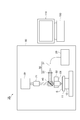
- FIG. 1 is a configuration diagram of the inspection device 1 according to the present embodiment.
- the inspection device 1 is a device that inspects the sample S (object).
- Sample S is, for example, a semiconductor device in which a plurality of light emitting elements are formed on a wafer.
- the light emitting element is, for example, an LED, a mini LED, a ⁇ LED, an SLD element, a laser element, a vertical cavity laser element (VCSEL), or the like.
- the inspection device 1 determines the quality of each light emitting element by observing photoluminescence (specifically, fluorescence) of the plurality of light emitting elements formed in the sample S.
- the quality of the light emitting element can be determined, for example, by probing (that is, based on electrical characteristics).
- the quality of the light emitting element can be determined by acquiring a fluorescence image, so that a large number of light emitting elements can be used without being bound by physical restrictions. Good or bad can be judged efficiently.
- the inspection device 1 includes a chuck 11, an XY stage 12, an excitation light source 20, an optical system 30, a dichroic mirror 40, an objective lens 51, a Z stage 52, and a dichroic mirror 60.
- Optical element imaging lenses 71 and 72, cameras 81 (first imaging unit), 82 (second imaging unit), dark box 90, control device 100 (determination unit), monitor 110. , Is equipped.
- the dark box 90 accommodates configurations other than the control device 100 and the monitor 110 among the configurations described above, and is provided to prevent the influence of external light on each of the accommodated configurations. Even if each configuration housed in the dark box 90 is mounted on the vibration isolation table in order to improve the quality of the images captured by the cameras 81 and 82 (improve the image quality and prevent the image from being displaced). Good.
- the chuck 11 is a holding member that holds the sample S.
- the chuck 11 holds the sample S by, for example, vacuum-sucking the wafer of the sample S.
- the XY stage 12 is a stage for moving the chuck 11 holding the sample S in the XY directions (front-back / left-right directions), that is, in the direction along the mounting surface of the sample S in the chuck 11. In the XY stage 12, the chuck 11 is moved in the XY direction so that each of the plurality of light emitting elements is sequentially set as an irradiation region of the excitation light according to the control of the control device 100.
- the inspection device 1 may further include a rotation stage ( ⁇ stage, not shown).
- Such a rotating stage may be provided, for example, above the XY stage 12 and below the chuck 11, or may be provided integrally with the XY stage 12.
- the rotation stage is for accurately aligning the vertical and horizontal positions of the sample S. By providing the rotating stage, it is possible to shorten the time for alignment and the like, and shorten the total time for data processing.
- the excitation light source 20 is a light source that generates excitation light to be irradiated to the sample S and irradiates the sample S with the excitation light.
- the excitation light source 20 may be a light source capable of generating light including a wavelength that excites the light emitting element of the sample S, and is, for example, an LED, a laser, a halogen lamp, a mercury lamp, a D2 lamp, a plasma light source, or the like.
- the inspection device 1 may further include a sensor that monitors the illumination brightness in order to keep the brightness of the excitation light emitted from the excitation light source 20 constant.
- the optical system 30 includes an optical fiber cable 31 and a light guide lens 32.
- the optical fiber cable 31 is a light guide optical fiber cable connected to the excitation light source 20.
- the light guide lens 32 is, for example, a single or composite convex lens, and guides the excitation light arriving through the optical fiber cable 31 toward the dichroic mirror 40.
- the inspection device 1 is provided with a bandpass filter (not shown) between the excitation light source 20 and the dichroic mirror 40 in order to prevent the wavelength of the excitation light emitted from the excitation light source 20 from changing over time. You may.
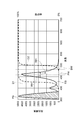
- the dichroic mirror 40 is a mirror created by using a special optical material, and reflects light of a specific wavelength and transmits light of other wavelengths. Specifically, the dichroic mirror 40 reflects the excitation light in the direction of the objective lens 51, and photoluminescence (specifically, fluorescence) from the light emitting element, which is light in a wavelength band different from the excitation light, is transmitted in the direction of the dichroic mirror 60. It is configured to be transparent to. As shown in FIG. 2, the region of the normal emission spectrum FS of the excitation light is on the lower wavelength side than the region of the normal emission spectrum (normal fluorescence spectrum) ES of fluorescence.
- the dichroic mirror 40 reflects the excitation light, which is light in the low wavelength band, in the direction of the objective lens 51, and transmits fluorescence, which is light in the higher wavelength band than the excitation light, in the direction of the dichroic mirror 60.
- the objective lens 51 has a configuration for observing the sample S, and collects the excitation light guided by the dichroic mirror 40 on the sample S.
- the Z stage 52 adjusts the focus by moving the objective lens 51 in the Z direction (vertical direction), that is, in the direction intersecting the mounting surface of the sample S on the chuck 11.
- the dichroic mirror 60 is a mirror created by using a special optical material, and reflects light of a specific wavelength and transmits light of other wavelengths.
- the dichroic mirror 60 separates the fluorescence from the light emitting element into fluorescence having a wavelength longer than the first wavelength and fluorescence having a wavelength shorter than the second wavelength.
- the first wavelength and the second wavelength will be described as having the same wavelength (reference wavelength BW). That is, the dichroic mirror 60 separates the fluorescence from the light emitting element into fluorescence having a wavelength longer than the reference wavelength BW and fluorescence having a wavelength shorter than the reference wavelength BW.
- FIG. 2 is a diagram for explaining the emission spectrum and the characteristics of the dichroic mirrors 60 and 40.
- the horizontal axis represents the wavelength
- the left vertical axis represents the emission brightness
- the right vertical axis represents the transmittance.
- the above-mentioned reference wavelength BW is defined as the peak wavelength PW of the normal fluorescence spectrum ES of the light emitting element plus the full width at half maximum WH of the normal fluorescence spectrum ES.
- the dichroic mirror 60 does not transmit (reflect) fluorescence having a wavelength shorter than the reference wavelength BW and is longer than the reference wavelength BW. It is configured to transmit wavelength fluorescence.
- the dichroic mirror 40 reflects the light in the wavelength band of the normal emission spectrum FS of the excitation light, and the light in the wavelength band of the normal fluorescence spectrum ES. Is almost transparent.
- the short wavelength fluorescence reflected by the dichroic mirror 60 is the fluorescence of the wavelength included in the normal fluorescence spectrum ES (the fluorescence of the emission wavelength originally), and the dichroic mirror 60
- the long-wavelength fluorescence transmitted through is the fluorescence of a wavelength not included in the normal fluorescence spectrum ES (fluorescence on the long wavelength side).
- the emission wavelength may be, for example, a wavelength known in advance from the specifications of the light emitting element, or may be a wavelength at which the intensity of fluorescence from the light emitting element is measured by a spectroscope.
- the dichroic mirror 60 transmits a part of the fluorescence having a wavelength shorter than the reference wavelength BW and reflects a part of the fluorescence having a wavelength longer than the reference wavelength BW (see FIG. 2).
- the dichroic mirror 60 has a wavelength shorter than the reference wavelength BW. It reflects the fluorescence of the above and transmits the fluorescence of a wavelength longer than the reference wavelength BW.
- Fluorescence having a wavelength longer than the reference wavelength BW reaches the imaging lens 71 via the dichroic mirror 60. Fluorescence having a wavelength shorter than the reference wavelength BW (fluorescence having an originally emitting wavelength) reaches the imaging lens 72 via the dichroic mirror 60.
- the imaging lens 71 is a lens that forms an image of fluorescence on the long wavelength side and guides the fluorescence to the camera 81.
- the camera 81 is an imaging unit that captures fluorescence from sample S. More specifically, the camera 81 captures fluorescence having a wavelength longer than the reference wavelength BW (fluorescence on the long wavelength side) among the fluorescence from the light emitting element. The camera 81 captures fluorescence on the long wavelength side by detecting an image formed by the imaging lens 71. The camera 81 outputs a fluorescence image on the long wavelength side, which is the imaging result, to the control device 100.
- the camera 81 is an area image sensor such as a CCD or MOS.
- the camera 81 may be composed of a line sensor or a TDI (Time Delay Integration) sensor.
- the inspection device 1 may further include a bandpass filter between the dichroic mirror 60 and the camera 81 in order to prevent unnecessary light emission on the long wavelength side.
- the imaging lens 72 is a lens that originally forms fluorescence of an emission wavelength and guides the fluorescence to the camera 82.
- the camera 82 is an imaging unit that captures fluorescence from sample S. More specifically, the camera 82 is a fluorescence having a wavelength shorter than the reference wavelength BW among the fluorescence from the light emitting element and having a wavelength included in the normal fluorescence spectrum ES (see FIG. 2) of the light emitting element (original emission wavelength). Fluorescence) is imaged.
- the camera 82 originally captures the fluorescence of the emission wavelength by detecting the image formed by the imaging lens 72.
- the camera 82 outputs a fluorescence image having an originally emitting wavelength, which is an imaging result, to the control device 100.
- the camera 82 is an area image sensor such as a CCD or MOS. Further, the camera 82 may be composed of a line sensor or a TDI sensor.
- the inspection device 1 further installs a bandpass filter between the dichroic mirror 60 and the camera 82 in order to prevent the fluorescence on the long wavelength side from being mixed due to the surface reflection of the dichroic mirror 60 when measuring the fluorescence on the short wavelength side. You may have it.
- the control device 100 controls the XY stage 12, the excitation light source 20, the Z stage 52, and the cameras 81 and 82. Specifically, the control device 100 adjusts the irradiation region of the excitation light (irradiation region in the sample S) by controlling the XY stage 12. The control device 100 adjusts the focus related to the excitation light by controlling the Z stage 52. The control device 100 adjusts the emission of the excitation light and the wavelength and amplitude of the excitation light by controlling the excitation light source 20. The control device 100 controls the cameras 81 and 82 to make adjustments related to the acquisition of the fluorescence image.
- the control device 100 determines the quality of the light emitting element of the sample S based on the fluorescence images captured by the cameras 81 and 82 (details will be described later).
- the control device 100 is a computer, and is physically configured to include a memory such as a RAM and a ROM, a processor (arithmetic circuit) such as a CPU, a communication interface, and a storage unit such as a hard disk. Examples of the control device 100 include personal computers, cloud servers, smart devices (smartphones, tablet terminals, etc.) and the like.
- the control device 100 functions by executing a program stored in the memory on the CPU of the computer system.
- the monitor 110 is a display device that displays a fluorescence image that is a measurement result.
- control device 100 related to the quality determination of the light emitting element
- the control device 100 is based on the fluorescence image on the long wavelength side (first fluorescence image) acquired by the camera 81 and the fluorescence image of the original emission wavelength (second fluorescence image) acquired by the camera 82. Judge the quality of the light emitting element. For example, the control device 100 determines the quality of the light emitting element based on the fluorescence image of the original emission wavelength acquired by the camera 82, and after the determination, the camera 81 determines that the light emitting element is good in the determination. The quality is judged based on the fluorescence image on the long wavelength side acquired by.
- the control device 100 first identifies the position of the light emitting element based on the fluorescence image, and specifies the light emitting area of each light emitting element.
- the position of the light emitting element is specified, for example, by converting the position in the fluorescence image with the position of the XY stage 12.
- the control device 100 may acquire a pattern image of the entire sample S in advance and recognize (specify) the position of the light emitting element from the pattern image or the fluorescence image. Then, the control device 100 derives the average brightness in the light emitting area of each light emitting element based on the fluorescence image of the originally emitting wavelength, and associates the address position and the brightness (average brightness in the light emitting area) with each light emitting element. ..
- the control device 100 derives an evaluation index from the absolute brightness and the relative brightness for each address (each light emitting element).
- the relative brightness is the brightness ratio of the light emitting element to be derived to the average brightness of the light emitting element group including the light emitting element to be derived and the light emitting elements around the light emitting element.
- the control device 100 derives an evaluation index from, for example, the product of the absolute brightness and the relative brightness.
- the control device 100 derives an evaluation index from the product of the absolute brightness and the relative brightness to the nth power (n is a natural number, for example, 2).
- the control device 100 derives the above-mentioned evaluation index for each light emitting element included in the same fluorescence image.
- the control device 100 acquires a new fluorescence image (a fluorescence image having an originally emitting wavelength) by changing the irradiation region, and derives an evaluation index for each light emitting element included in the fluorescence image.
- the control device 100 sorts (sorts) the light emitting elements in descending order of the evaluation index.
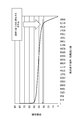
- FIG. 3 is a diagram showing a sorting result of light emitting elements according to an evaluation index.
- the vertical axis shows the evaluation index according to the magnitude of the brightness
- the horizontal axis shows the order of each light emitting element.
- the evaluation index sharply decreases at a certain point (change point).
- the control device 100 determines that a light emitting element having an evaluation index equal to or higher than the threshold value is a good product (good pixel) and a light emitting element smaller than the threshold value is a defective product (defective pixel), using such a change point as a threshold value. May be good.
- a threshold value for example, a reference semiconductor device for determining the threshold value is used in advance, and the quality judgment result of the light emitting device based on fluorescence (photoluminescence) and the quality judgment result based on probing (good / bad judgment result based on electrical characteristics) are set. ) May be compared with.
- control device 100 detects bright spots (fluorescent spots) in the light emitting area of each light emitting element based on the fluorescence image on the long wavelength side, and associates the address position and the number of bright spots with each light emitting element.
- a bright spot (emission spot) on the longer wavelength side than the normal emission spectrum is an abnormal emission point.
- the control device 100 determines whether or not a certain number or more of bright spots are included in the fluorescence image on the long wavelength side of the light emitting element determined to be a good product in the quality determination based on the fluorescence image of the originally emission wavelength described above.
- a light emitting element that does not contain a certain number or more of bright spots is judged as a good product (good pixel), and a light emitting element that contains a certain number or more of bright spots is judged as a defective product (defective pixel).
- a light emitting element that is originally determined to be a good product based on a fluorescence image of an emission wavelength may be determined to be a defective product based on a fluorescence image on the long wavelength side.
- the control device 100 determines the non-defective product of the light emitting element based on the fluorescence image of the original emission wavelength acquired by the camera 82, and then acquires the light emitting element determined to be defective in the determination by the camera 81.
- the quality may be determined based on the fluorescence image on the long wavelength side. Further, the control device 100 may perform quality determination based on the fluorescence image on the long wavelength side for all the light emitting elements. In this way, the control device 100 may make a pass / fail judgment based on the fluorescence image on the long wavelength side only for the light emitting element that is originally determined to be good based on the fluorescence image of the emission wavelength, or may determine the quality based on the fluorescence image of the emission wavelength.
- Only the light emitting element determined to be defective based on the image may be judged to be good or bad based on the fluorescence image on the long wavelength side, or all the light emitting elements may be judged regardless of the quality judgment result based on the fluorescence image of the originally emitting wavelength. May be judged based on the fluorescence image on the long wavelength side.
- the control device 100 outputs the quality determination result of each light emitting element.
- the pass / fail determination result is displayed on the monitor 110, for example. Further, the control device 100 may identify a defective portion (for example, a bright spot on the long wavelength side) in the light emitting element and output the position of the defective portion (output as displayed on the monitor 110). ..
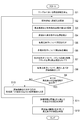
- FIG. 4 is a flowchart of an inspection method executed by the inspection device 1.
- the irradiation region in the sample S is first determined (step S1). Specifically, the control device 100 determines the irradiation region of the excitation light by controlling the XY stage 12.
- the excitation light source 20 irradiates the irradiation region of the sample S with excitation light according to the control of the control device 100 (step S2, excitation light irradiation step).
- the excitation light source 20 generates and emits light including a wavelength that excites the light emitting element of the sample S.
- the excitation light reaches the dichroic mirror 40 via the optical fiber cable 31 and the light guide lens 32 of the optical system 30, is reflected by the dichroic mirror 40, and is focused on the irradiation region of the sample S via the objective lens 51.
- the light emitting element of sample S fluoresces in response to the excitation light.
- the fluorescence passes through the dichroic mirror 40 and is separated into the fluorescence of the originally emitting wavelength and the fluorescence of the long wavelength side in the dichroic mirror 60 (separation step).
- the fluorescence of the emission wavelength is imaged by the imaging lens 72 and guided to the camera 82.
- the fluorescence on the long wavelength side is imaged by the imaging lens 71 and guided to the camera 81.
- the camera 81 images the fluorescence on the long wavelength side (step S3, the first imaging step). Further, the camera 82 originally captures the fluorescence of the emission wavelength (step S3, the second imaging step). The cameras 81 and 82 output the fluorescence image which is the imaging result to the control device 100.
- the control device 100 specifies the position of the light emitting element based on the fluorescence image (step S4), and specifies the light emitting area in each light emitting element. Then, the control device 100 derives the brightness (average brightness) in the light emitting area of each light emitting element based on the fluorescence image of the originally emitting wavelength (step S5). Further, the control device 100 detects bright spots (fluorescent spots) in the light emitting area of each light emitting element based on the fluorescence image on the long wavelength side, and derives the number of bright spots (step S6). Then, the control device 100 associates the address position with the brightness (average brightness) and associates the address position with the number of bright spots for each light emitting element (step S7).
- the control device 100 derives an evaluation index from the absolute brightness and the relative brightness for each light emitting element (step S8).
- the control device 100 derives an evaluation index from, for example, the product of the absolute brightness and the relative brightness.
- the control device 100 derives an evaluation index from the product of the absolute brightness and the relative brightness to the nth power (n is a natural number, for example, 2).
- control device 100 determines whether or not the above-mentioned evaluation index has been derived for all the light emitting elements (light emitting elements to be determined) of the sample S (step S9). If it is determined in step S9 that it has not been derived, the control device 100 determines a new irradiation region so that the light emitting element before deriving the evaluation index is included (step S10). After that, the processing after step S2 is performed again.
- the control device 100 determines the quality of the light emitting elements by comparing the evaluation indexes of each light emitting element with a predetermined threshold value. (Step S11. Judgment step). Specifically, the control device 100 sorts (sorts) the light emitting elements in descending order of the evaluation index, and selects the light emitting elements having the evaluation index equal to or higher than the threshold value (good pixels) and the light emitting elements smaller than the threshold value. Determined as defective (defective pixel).
- control device 100 determines the quality of the light emitting element by comparing the number of bright spots included in the fluorescence image on the long wavelength side with a predetermined threshold value (step S12, determination step). Specifically, the control device 100 refers to a light emitting element (good pixel) that does not contain a certain number or more of bright spots in the fluorescence image on the long wavelength side, and a light emitting element that contains a certain number or more of bright spots. Is determined to be a defective product (defective pixel). The control device 100 may output the quality determination result of each light emitting element. Further, the control device 100 may identify a defective portion (for example, a bright spot on the long wavelength side) in the light emitting element and output the position of the defective portion (output as displayed on the monitor 110). ..
- the inspection device 1 is an inspection device for inspecting a sample S in which a plurality of light emitting elements are formed, and is an excitation light source 20 that generates excitation light to be irradiated on the sample S and fluorescence from the light emitting element.
- the light emitting element is based on the camera 81 that captures fluorescence having a wavelength longer than the reference wavelength BW (see FIG. 2) and the fluorescence image on the long wavelength side (first fluorescence image) acquired by the camera 81.
- the control device 100 for determining the quality is provided, and the reference wavelength BW is a wavelength obtained by adding the half-value full-width WH of the normal fluorescence spectrum ES to the peak wavelength PW of the normal fluorescence spectrum ES of the light emitting element (see FIG. 2).
- the quality of the light emitting element is determined based on the fluorescence image on the side.
- 5A and 5B are fluorescence images of the light emitting element L1 in an abnormal light emitting state, where FIG. 5A is a fluorescence image of an originally emitting wavelength and FIG. As shown in FIG.
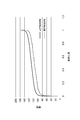
- FIG. 6 is a diagram showing the luminance distribution of the light emitting element in the abnormal light emitting state and the luminance distribution of the light emitting element in the normal light emitting state.
- the vertical axis shows the brightness and the horizontal axis shows the cumulative ratio.
- the light emitting element in the abnormal light emitting state has a lower brightness than the light emitting element in the normal light emitting state.
- the light emitting element in the abnormal light emitting state in which the fluorescent spot is generated on the long wavelength side has low brightness, and therefore needs to be determined as a defective product.
- the quality of the light emitting element is determined based on the fluorescence image on the long wavelength side, so that the above-mentioned fluorescence spot on the long wavelength side can be appropriately detected and the fluorescence.
- a light emitting element having a spot can be appropriately determined to be defective. That is, according to the inspection device 1, the quality of the light emitting element can be determined with high accuracy by considering the fluorescence on the long wavelength side.
- the inspection device 1 includes a dichroic mirror 60 that separates fluorescence from the light emitting element into fluorescence on the long wavelength side and fluorescence of the original emission wavelength, and fluorescence of the original emission wavelength and a wavelength included in the normal fluorescence spectrum of the light emitting element. It includes a camera 82 that captures fluorescence. According to such a configuration, both the fluorescence on the long wavelength side and the fluorescence of the wavelength included in the normal fluorescence spectrum are imaged without time loss. As a result, not only the abnormal light emission on the long wavelength side but also the light emission in the normal fluorescence spectrum can be appropriately detected for each light emitting element, and the light emitting state of each light emitting element can be acquired in more detail. Then, by separating the fluorescence with the dichroic mirror 60, it is possible to easily and surely image the fluorescence on the long wavelength side and the fluorescence of the wavelength included in the normal fluorescence spectrum described above.
- the control device 100 determines the quality of the light emitting element based on the fluorescence image on the long wavelength side and the fluorescence image of the original emission wavelength (second fluorescence image) acquired by the camera 82.
- the quality of the light emitting element can be determined based on the fluorescence of the wavelength included in the normal fluorescence spectrum. This makes it possible to determine the quality of the light emitting element with higher accuracy in consideration of both the abnormality (fluorescence spot) on the long wavelength side and the light emission state in the normal fluorescence spectrum.
- the control device 100 determines the quality of the light emitting element based on the fluorescence image of the emission wavelength, and after the determination, the light emitting element determined to be good in the determination is good or bad based on the fluorescence image on the long wavelength side. May be determined. According to such a configuration, after the light emitting element having an abnormal light emitting state in the normal fluorescence spectrum is appropriately determined to be defective, further, even if the light emitting state in the normal fluorescence spectrum is normal, the abnormality on the long wavelength side (fluorescence).
- a light emitting element having a spot can be determined to be defective, and a defective light emitting element can be identified without omission in consideration of both the light emitting state on the long wavelength side and the light emitting state in the normal fluorescence spectrum.
- the quality judgment based on the fluorescence image on the long wavelength side is performed only for the light emitting element that is originally judged to be good in the quality judgment based on the fluorescence image of the emission wavelength, the time required for the judgment on the abnormality on the long wavelength side is required. It can be shortened.
- the control device 100 determines the quality of the light emitting element based on the fluorescence image of the emission wavelength, and after the determination, the light emitting element determined to be defective in the determination is good or bad based on the fluorescence image on the long wavelength side. May be determined. According to such a configuration, for example, even if the light emitting element is determined to be defective based on the light emitting state in the normal fluorescence spectrum, the light emitting element having no abnormality (fluorescence spot) on the long wavelength side is considered to be good. It can be determined, and it is possible to avoid that a light emitting element having no serious abnormality (fluorescent spot on the long wavelength side) is determined to be defective.
- the quality judgment based on the fluorescence image on the long wavelength side is performed only for the light emitting element that is originally judged to be defective in the quality judgment based on the fluorescence image of the emission wavelength, the time required for the judgment related to the abnormality on the long wavelength side is required. It can be shortened.
- the control device 100 determines the quality of the light emitting element based on the brightness of the fluorescence image of the emission wavelength, and determines the quality of the light emitting element based on the bright spot included in the fluorescence image on the long wavelength side. According to such a configuration, the quality of the light emitting element is determined with higher accuracy in consideration of the brightness of fluorescence in the normal fluorescence spectrum and the information of the fluorescence spots on the long wavelength side (presence or absence and number of abnormal fluorescence spots, etc.). It can be performed.
- the control device 100 outputs the quality determination result of each light emitting element. Thereby, the quality determination result of each light emitting element can be used to identify the light emitting element affecting the luminous efficiency and take measures to improve the luminous efficiency.
- the control device 100 identifies a defective portion in the light emitting element and outputs the position of the defective portion. For example, by specifying the position of the fluorescence spot on the long wavelength side in the light emitting element based on the imaging result and outputting the position of the fluorescence spot as a defective part, the luminous efficiency is based on the information of the defective part. Can be taken to improve.
- the present invention is not limited to the above embodiment.
- the first wavelength and the second wavelength have been described as being the same wavelength (reference wavelength BW), the wavelength is not limited to this and may be different from each other.
- the quality of the light emitting element is determined based on the fluorescence on the long wavelength side and the fluorescence of the originally emitting wavelength, but the present invention is not limited to this, and the control device 100 (determination unit) is the length imaged by the camera 81.
- the quality of the light emitting element may be determined based only on the fluorescence on the wavelength side.
- the inspection device 1A only needs to have one camera 81 and an imaging lens 71 corresponding to the camera 81, and originally acquires fluorescence of the emission wavelength. It is not necessary to have the configuration for this purpose (the dichroic mirror 60, the camera 82, and the imaging lens 72 shown in FIG. 1).
- the quality determination of the light emitting element based on the fluorescence on the long wavelength side it has been described as determining whether or not the fluorescence image contains a certain number or more of bright spots, but the present invention is not limited to this, and the fluorescence image is simply used.
- the quality of the light emitting element may be determined depending on whether or not one or more bright spots are included.
- the dichroic mirror 60 has been described by using a dichroic mirror 60 having a steep change in transmittance (reflectance) with respect to a wavelength, as shown in FIG. 2, but the present invention has a dichroic with such characteristics. It is not limited to using a mirror.
- a dichroic mirror may be used in which the transmittance (reflectance) with respect to the wavelength gradually changes with a width of about 100 nm. In such a dichroic mirror, in a specific wavelength band, the fluorescence transmittance (reflectance) changes according to the change in wavelength, and the wavelength band other than the specific wavelength band (lower wavelength side than the specific wavelength band).
- the transmittance (reflectance) of fluorescence is constant regardless of the change in wavelength.
- the width of the wavelength band in which the fluorescence transmittance (reflectance) changes according to the change in wavelength is defined as the "edge shift width”
- the edge shift width of such a dichroic mirror is, for example, the normal fluorescence spectrum of the light emitting element. It may be wider than the full width at half maximum.
- 1,1A ... Inspection device 20 ... Excitation light source, 60 ... Dichroic mirror (optical element), 81 ... Camera (first imaging unit), 82 ... Camera (second imaging unit), 100 ... Control device (judgment unit) ).
Abstract
The present invention provides an inspection device for inspecting a sample in which a plurality of light-emitting elements are formed, wherein: the inspection device is provided with an excitation light source for generating excitation light beamed onto the sample, a camera for imaging fluorescence having a wavelength greater than a reference wavelength from among fluorescence from the light-emitting elements, and a control device for assessing the quality of the light-emitting elements on the basis of the fluorescence imaged by the camera. The reference wavelength is the wavelength obtained by adding the full width at half maximum of a normal fluorescence spectrum of the light-emitting elements to the peak wavelength of the normal fluorescence spectrum.
Description
本発明の一態様は、検査装置及び検査方法に関する。
One aspect of the present invention relates to an inspection device and an inspection method.
ウェハ上に形成された発光素子群の良・不良を判定する手法として、発光素子が発するフォトルミネッセンスを観察し、該フォトルミネッセンスの輝度に基づいて発光素子の良否判定を行う手法が知られている(例えば特許文献1参照)。
As a method for determining the quality of a group of light emitting elements formed on a wafer, a method of observing the photoluminescence emitted by the light emitting element and determining the quality of the light emitting element based on the brightness of the photoluminescence is known. (See, for example, Patent Document 1).
特許文献1に記載された検査方法では、発光素子からの蛍光を分割して、複数のカメラそれぞれにおいて互いに異なる波長の蛍光を撮像し、それぞれの観察輝度値の比率に基づいて、観察対象部位から発せられる光の推定波長を算出している。
In the inspection method described in Patent Document 1, the fluorescence from the light emitting element is divided, the fluorescence of different wavelengths is imaged by each of a plurality of cameras, and the fluorescence from the observation target portion is determined based on the ratio of the observation luminance values. The estimated wavelength of the emitted light is calculated.
ここで、特許文献1に記載されたような検査方法は、正常発光スペクトルの蛍光にのみ着目している。しかしながら、一部の発光素子では正常発光スペクトルよりも長波長側に発光スポットが生じる場合がある。上述した検査方法においては、このような長波長側の蛍光を考慮して発光素子の良否判定を行うことができず、発光素子の良否判定を高精度に行うことができない場合がある。
Here, the inspection method as described in Patent Document 1 focuses only on the fluorescence of the normal emission spectrum. However, in some light emitting elements, a light emitting spot may occur on the longer wavelength side than the normal light emitting spectrum. In the above-described inspection method, the quality of the light emitting element cannot be determined in consideration of the fluorescence on the long wavelength side, and the quality of the light emitting element may not be determined with high accuracy.
本発明の一態様は上記実情に鑑みてなされたものであり、発光素子の良否判定を高精度に行うことを目的とする。
One aspect of the present invention has been made in view of the above circumstances, and an object of the present invention is to determine the quality of a light emitting element with high accuracy.
本発明の一態様に係る検査装置は、複数の発光素子が形成された対象物を検査する検査装置であって、対象物に照射される励起光を生成する励起光源と、発光素子からの蛍光のうち、第1の波長よりも長い波長の蛍光を撮像する第1の撮像部と、第1の撮像部によって取得された第1の蛍光画像に基づいて、発光素子の良否を判定する判定部と、を備え、第1の波長は、発光素子の正常蛍光スペクトルのピーク波長に該正常蛍光スペクトルの半値全幅を加えた波長である。
The inspection device according to one aspect of the present invention is an inspection device that inspects an object on which a plurality of light emitting elements are formed, and is an excitation light source that generates excitation light to irradiate the object and fluorescence from the light emitting element. Of these, a first imaging unit that captures fluorescence having a wavelength longer than the first wavelength, and a determination unit that determines the quality of the light emitting element based on the first fluorescence image acquired by the first imaging unit. The first wavelength is a wavelength obtained by adding the half-value full width of the normal fluorescence spectrum to the peak wavelength of the normal fluorescence spectrum of the light emitting element.
本発明の一態様に係る検査装置によれば、発光素子の正常蛍光スペクトルのピーク波長に正常蛍光スペクトルの半値全幅を加えた波長の蛍光画像、すなわち発光素子の正常蛍光スペクトルに含まれ得ない長波長側の蛍光画像に基づいて、発光素子の良否判定が行われる。一部の発光素子では正常蛍光スペクトルよりも長波長側に蛍光スポットが生じることがあるところ、このような長波長側の蛍光画像に基づいて発光素子の良否判定が行われることによって、上述した長波長側の蛍光スポットを適切に検出し、該蛍光スポットを有する発光素子を適切に不良と判定することができる。すなわち、本発明の一態様に係る検査装置によれば、長波長側の蛍光を考慮することにより発光素子の良否判定を高精度に行うことができる。
According to the inspection apparatus according to one aspect of the present invention, a fluorescence image having a wavelength obtained by adding the half-value full width of the normal fluorescence spectrum to the peak wavelength of the normal fluorescence spectrum of the light emitting element, that is, a length that cannot be included in the normal fluorescence spectrum of the light emitting element. The quality of the light emitting element is determined based on the fluorescence image on the wavelength side. In some light emitting elements, a fluorescence spot may occur on the longer wavelength side than the normal fluorescence spectrum. However, the quality of the light emitting element is determined based on such a fluorescence image on the long wavelength side, so that the above-mentioned length is obtained. The fluorescent spot on the wavelength side can be appropriately detected, and the light emitting element having the fluorescent spot can be appropriately determined to be defective. That is, according to the inspection device according to one aspect of the present invention, the quality of the light emitting element can be determined with high accuracy by considering the fluorescence on the long wavelength side.
検査装置は、発光素子からの蛍光を、第1の波長よりも長い波長の蛍光及び第2の波長よりも短い波長の蛍光に分離する光学素子と、第2の波長よりも短い波長の蛍光であって発光素子の正常蛍光スペクトルに含まれる波長の蛍光を撮像する第2の撮像部と、を更に備えていてもよい。このような構成によれば、長波長側の蛍光、及び、正常蛍光スペクトルに含まれる波長の蛍光の双方がタイムロスなく撮像される。このことで、各発光素子について、長波長側の異常発光だけでなく、正常蛍光スペクトルにおける発光についても適切に検出することができ、各発光素子の発光状態をより詳細に取得することができる。
The inspection device uses an optical element that separates fluorescence from the light emitting element into fluorescence having a wavelength longer than the first wavelength and fluorescence having a wavelength shorter than the second wavelength, and fluorescence having a wavelength shorter than the second wavelength. It may further include a second imaging unit that captures fluorescence of a wavelength included in the normal fluorescence spectrum of the light emitting element. According to such a configuration, both the fluorescence on the long wavelength side and the fluorescence of the wavelength included in the normal fluorescence spectrum are imaged without time loss. As a result, not only the abnormal light emission on the long wavelength side but also the light emission in the normal fluorescence spectrum can be appropriately detected for each light emitting element, and the light emitting state of each light emitting element can be acquired in more detail.
第1の波長と第2の波長とは同じ波長であり、光学素子はダイクロイックミラーであってもよい。このような構成によれば、上述した長波長側の蛍光及び正常蛍光スペクトルに含まれる波長の蛍光を簡易且つ確実に撮像することができる。
The first wavelength and the second wavelength are the same wavelength, and the optical element may be a dichroic mirror. According to such a configuration, the fluorescence on the long wavelength side and the fluorescence of the wavelength included in the normal fluorescence spectrum can be easily and surely imaged.
判定部は、第1の蛍光画像及び第2の撮像部によって取得された第2の蛍光画像に基づいて、発光素子の良否を判定してもよい。これにより、長波長側の蛍光を考慮して発光素子の良否判定を行うことに加えて、正常蛍光スペクトルに含まれる波長の蛍光に基づき発光素子の良否判定を行うことができる。このことで、長波長側の異常(蛍光スポット)及び正常蛍光スペクトルにおける発光状態の双方を考慮して、より高精度に発光素子の良否判定を行うことができる。
The determination unit may determine the quality of the light emitting element based on the first fluorescence image and the second fluorescence image acquired by the second imaging unit. As a result, in addition to determining the quality of the light emitting element in consideration of the fluorescence on the long wavelength side, the quality of the light emitting element can be determined based on the fluorescence of the wavelength included in the normal fluorescence spectrum. This makes it possible to determine the quality of the light emitting element with higher accuracy in consideration of both the abnormality (fluorescence spot) on the long wavelength side and the light emission state in the normal fluorescence spectrum.
判定部は、第2の蛍光画像に基づいて発光素子の良否を判定すると共に、該判定の後に、該判定において良と判定された発光素子について、第1の蛍光画像に基づいて良否を判定してもよい。このような構成によれば、正常蛍光スペクトルにおける発光状態が異常である発光素子を適切に不良と判定した後に、さらに、正常蛍光スペクトルにおける発光状態が正常であっても長波長側の異常(蛍光スポット)を有する発光素子を不良と判定することができ、長波長側の発光状態及び正常蛍光スペクトルにおける発光状態の双方を考慮して、不良である発光素子を漏れなく特定することができる。また、第2の蛍光画像に基づく良否判定において良と判定された発光素子についてのみ、第1の蛍光画像に基づく良否判定が行われるため、長波長側の異常に係る判定に要する時間を短縮することができる。
The determination unit determines the quality of the light emitting element based on the second fluorescence image, and after the determination, determines the quality of the light emitting element determined to be good in the determination based on the first fluorescence image. You may. According to such a configuration, after the light emitting element having an abnormal light emitting state in the normal fluorescence spectrum is appropriately determined to be defective, further, even if the light emitting state in the normal fluorescence spectrum is normal, the abnormality on the long wavelength side (fluorescence). A light emitting element having a spot) can be determined to be defective, and a defective light emitting element can be identified without omission in consideration of both the light emitting state on the long wavelength side and the light emitting state in the normal fluorescence spectrum. Further, since the quality determination based on the first fluorescence image is performed only for the light emitting element determined to be good in the quality determination based on the second fluorescence image, the time required for the determination related to the abnormality on the long wavelength side is shortened. be able to.
判定部は、第2の蛍光画像に基づいて発光素子の良否を判定すると共に、該判定の後に、該判定において不良と判定された発光素子について、第1の蛍光画像に基づいて良否を判定してもよい。このような構成によれば、例えば、正常蛍光スペクトルにおける発光状態に基づいて不良と判定された発光素子であっても、長波長側の異常(蛍光スポット)を有さない発光素子については良と判定することができ、深刻な異常(長波長側の蛍光スポット)を有さない発光素子が不良と判定されることを回避することができる。また、第2の蛍光画像に基づく良否判定において不良と判定された発光素子についてのみ、第1の蛍光画像に基づく良否判定が行われるため、長波長側の異常に係る判定に要する時間を短縮することができる。
The determination unit determines the quality of the light emitting element based on the second fluorescence image, and after the determination, determines the quality of the light emitting element determined to be defective in the determination based on the first fluorescence image. You may. According to such a configuration, for example, even if the light emitting element is determined to be defective based on the light emitting state in the normal fluorescence spectrum, the light emitting element having no abnormality (fluorescence spot) on the long wavelength side is considered to be good. It can be determined, and it is possible to avoid that a light emitting element having no serious abnormality (fluorescent spot on the long wavelength side) is determined to be defective. Further, since the quality determination based on the first fluorescence image is performed only for the light emitting element determined to be defective in the quality determination based on the second fluorescence image, the time required for the determination regarding the abnormality on the long wavelength side is shortened. be able to.
判定部は、第2の蛍光画像の輝度に基づいて発光素子の良否を判定すると共に、第1の蛍光画像に含まれる輝点に基づいて発光素子の良否を判定してもよい。このような構成によれば、正常蛍光スペクトルにおける蛍光の輝度と、長波長側の蛍光スポットの情報(異常蛍光スポットの有無や数等)とを考慮して、より高精度に発光素子の良否判定を行うことができる。
The determination unit may determine the quality of the light emitting element based on the brightness of the second fluorescence image, and may determine the quality of the light emitting element based on the bright spot included in the first fluorescence image. According to such a configuration, the quality of the light emitting element is determined with higher accuracy in consideration of the brightness of fluorescence in the normal fluorescence spectrum and the information of the fluorescence spots on the long wavelength side (presence or absence and number of abnormal fluorescence spots, etc.). It can be performed.
判定部は、各発光素子の良否判定結果を出力してもよい。これにより、各発光素子の良否判定結果を利用して、発光効率に影響を与えている発光素子を特定し、発光効率を向上させるための対処を行うことができる。
The judgment unit may output the quality judgment result of each light emitting element. Thereby, the quality determination result of each light emitting element can be used to identify the light emitting element affecting the luminous efficiency and take measures to improve the luminous efficiency.
判定部は、発光素子内における不良個所を特定し、該不良個所の位置を出力してもよい。例えば、撮像結果に基づいて長波長側の蛍光スポットの位置を特定して、該蛍光スポットの位置を不良個所として出力することにより、不良個所の情報に基づいて、発光効率を向上させるための対処を行うことができる。
The determination unit may identify a defective portion in the light emitting element and output the position of the defective portion. For example, by specifying the position of the fluorescence spot on the long wavelength side based on the imaging result and outputting the position of the fluorescence spot as a defective part, measures for improving the luminous efficiency based on the information of the defective part. It can be performed.
本発明の一態様に係る検査方法は、複数の発光素子が形成された対象物を検査する検査方法であって、対象物に励起光を照射する励起光照射ステップと、発光素子からの蛍光のうち、第1の波長よりも長い波長の蛍光を撮像する第1の撮像ステップと、第1の撮像ステップにおいて取得された第1の蛍光画像に基づいて、発光素子の良否を判定する判定ステップと、を備え、第1の波長は、発光素子の正常蛍光スペクトルのピーク波長に該正常蛍光スペクトルの半値全幅を加えた波長である。
The inspection method according to one aspect of the present invention is an inspection method for inspecting an object on which a plurality of light emitting elements are formed, and is an excitation light irradiation step of irradiating the object with excitation light and fluorescence from the light emitting element. Among them, a first imaging step of imaging fluorescence having a wavelength longer than the first wavelength, and a determination step of determining the quality of the light emitting element based on the first fluorescence image acquired in the first imaging step. The first wavelength is the peak wavelength of the normal fluorescence spectrum of the light emitting element plus the full width of the half value of the normal fluorescence spectrum.
検査方法は、発光素子からの蛍光を、第1の波長よりも長い波長の蛍光及び第2の波長よりも短い波長の蛍光に分離する分離ステップと、第2の波長よりも短い波長の蛍光であって発光素子の正常蛍光スペクトルに含まれる波長の蛍光を撮像する第2の撮像ステップと、を更に備えていてもよい。
The inspection method consists of a separation step of separating the fluorescence from the light emitting element into fluorescence having a wavelength longer than the first wavelength and fluorescence having a wavelength shorter than the second wavelength, and fluorescence having a wavelength shorter than the second wavelength. It may further include a second imaging step of imaging fluorescence of a wavelength included in the normal fluorescence spectrum of the light emitting element.
第1の波長と第2の波長とは同じ波長であってもよい。
The first wavelength and the second wavelength may be the same wavelength.
判定ステップでは、第1の蛍光画像及び第2の撮像ステップにおいて取得された第2の蛍光画像に基づいて、発光素子の良否を判定してもよい。
In the determination step, the quality of the light emitting element may be determined based on the first fluorescence image and the second fluorescence image acquired in the second imaging step.
判定ステップでは、第2の蛍光画像に基づいて発光素子の良否を判定すると共に、該判定の後に、該判定において良と判定された発光素子について、第1の蛍光画像に基づいて良否を判定してもよい。
In the determination step, the quality of the light emitting element is determined based on the second fluorescence image, and after the determination, the quality of the light emitting element determined to be good in the determination is determined based on the first fluorescence image. You may.
判定ステップでは、第2の蛍光画像に基づいて発光素子の良否を判定すると共に、該判定の後に、該判定において不良と判定された発光素子について、第1の蛍光画像に基づいて良否を判定してもよい。
In the determination step, the quality of the light emitting element is determined based on the second fluorescence image, and after the determination, the quality of the light emitting element determined to be defective in the determination is determined based on the first fluorescence image. You may.
判定ステップでは、第2の蛍光画像の輝度に基づいて発光素子の良否を判定すると共に、第1の蛍光画像に含まれる輝点に基づいて発光素子の良否を判定してもよい。
In the determination step, the quality of the light emitting element may be determined based on the brightness of the second fluorescence image, and the quality of the light emitting element may be determined based on the bright spot included in the first fluorescence image.
判定ステップでは、各発光素子の良否判定結果を出力してもよい。
In the determination step, the quality determination result of each light emitting element may be output.
判定ステップでは、発光素子内における不良個所を特定し、該不良個所の位置を出力してもよい。
In the determination step, a defective portion in the light emitting element may be specified and the position of the defective portion may be output.
本発明の一態様によれば、発光素子の良否判定を高精度に行うことができる。
According to one aspect of the present invention, the quality of the light emitting element can be determined with high accuracy.
以下、本発明の実施形態について、図面を参照して詳細に説明する。なお、各図において同一又は相当部分には同一符号を付し、重複する説明を省略する。
Hereinafter, embodiments of the present invention will be described in detail with reference to the drawings. In each figure, the same or corresponding parts are designated by the same reference numerals, and duplicate description will be omitted.
図1は、本実施形態に係る検査装置1の構成図である。検査装置1は、サンプルS(対象物)を検査する装置である。サンプルSは、例えば、ウェハ上に複数の発光素子が形成された半導体デバイスである。発光素子は、例えばLED、ミニLED、μLED、SLD素子、レーザ素子、垂直型レーザ素子(VCSEL)等である。検査装置1は、サンプルSにおいて形成されている複数の発光素子について、フォトルミネッセンス(具体的には蛍光)を観察することにより、各発光素子の良否判定を行う。発光素子の良否判定は、例えばプロービングによって(すなわち電気的特性に基づいて)行うことが考えられる。しかしながら、例えばμLED等の微細なLEDについては、針をあてて計測を行うプロービングが物理的に困難である。この点、本実施形態に係るフォトルミネッセンスに基づく発光素子の良否判定方法は、蛍光画像を取得することによって良否判定を行うことができるので、物理的な制約にとらわれることなく、大量の発光素子を効率的に良否判定することができる。
FIG. 1 is a configuration diagram of the inspection device 1 according to the present embodiment. The inspection device 1 is a device that inspects the sample S (object). Sample S is, for example, a semiconductor device in which a plurality of light emitting elements are formed on a wafer. The light emitting element is, for example, an LED, a mini LED, a μLED, an SLD element, a laser element, a vertical cavity laser element (VCSEL), or the like. The inspection device 1 determines the quality of each light emitting element by observing photoluminescence (specifically, fluorescence) of the plurality of light emitting elements formed in the sample S. The quality of the light emitting element can be determined, for example, by probing (that is, based on electrical characteristics). However, for a fine LED such as a μLED, it is physically difficult to perform measurement by applying a needle. In this regard, in the photoluminescence-based quality determination method of the light emitting element according to the present embodiment, the quality of the light emitting element can be determined by acquiring a fluorescence image, so that a large number of light emitting elements can be used without being bound by physical restrictions. Good or bad can be judged efficiently.
図1に示されるように、検査装置1は、チャック11と、XYステージ12と、励起光源20と、光学系30と、ダイクロイックミラー40と、対物レンズ51と、Zステージ52と、ダイクロイックミラー60(光学素子)と、結像レンズ71,72と、カメラ81(第1の撮像部),82(第2の撮像部)と、暗箱90と、制御装置100(判定部)と、モニタ110と、を備えている。暗箱90は、上述した構成のうち制御装置100及びモニタ110以外の構成を収容しており、収容した各構成に外部の光の影響が及ぼされることを回避するために設けられている。なお、暗箱90に収容される各構成は、カメラ81,82において撮像される画像の質の向上(画質の向上及び画像の位置ずれ防止)を図るべく除振台の上に搭載されていてもよい。
As shown in FIG. 1, the inspection device 1 includes a chuck 11, an XY stage 12, an excitation light source 20, an optical system 30, a dichroic mirror 40, an objective lens 51, a Z stage 52, and a dichroic mirror 60. (Optical element), imaging lenses 71 and 72, cameras 81 (first imaging unit), 82 (second imaging unit), dark box 90, control device 100 (determination unit), monitor 110. , Is equipped. The dark box 90 accommodates configurations other than the control device 100 and the monitor 110 among the configurations described above, and is provided to prevent the influence of external light on each of the accommodated configurations. Even if each configuration housed in the dark box 90 is mounted on the vibration isolation table in order to improve the quality of the images captured by the cameras 81 and 82 (improve the image quality and prevent the image from being displaced). Good.
チャック11は、サンプルSを保持する保持部材である。チャック11は、例えばサンプルSのウェハを真空吸着することにより、サンプルSを保持する。XYステージ12は、サンプルSを保持しているチャック11をXY方向(前後・左右方向)、すなわちチャック11におけるサンプルSの載置面に沿った方向に移動させるステージである。XYステージ12は、制御装置100の制御に応じて、複数の発光素子のそれぞれが順次、励起光の照射領域とされるように、チャック11をXY方向に移動させる。なお、検査装置1は、更に回転ステージ(Θステージ。不図示)を備えていてもよい。このような回転ステージは、例えばXYステージ12の上且つチャック11の下に設けられていてもよいし、XYステージ12と一体的に設けられていてもよい。回転ステージは、サンプルSの縦横の位置を精度よく合わせるためのものである。回転ステージが設けられることによって、位置合わせ等の時間を短縮し、データ処理のトータル時間を短縮することができる。
The chuck 11 is a holding member that holds the sample S. The chuck 11 holds the sample S by, for example, vacuum-sucking the wafer of the sample S. The XY stage 12 is a stage for moving the chuck 11 holding the sample S in the XY directions (front-back / left-right directions), that is, in the direction along the mounting surface of the sample S in the chuck 11. In the XY stage 12, the chuck 11 is moved in the XY direction so that each of the plurality of light emitting elements is sequentially set as an irradiation region of the excitation light according to the control of the control device 100. The inspection device 1 may further include a rotation stage (Θ stage, not shown). Such a rotating stage may be provided, for example, above the XY stage 12 and below the chuck 11, or may be provided integrally with the XY stage 12. The rotation stage is for accurately aligning the vertical and horizontal positions of the sample S. By providing the rotating stage, it is possible to shorten the time for alignment and the like, and shorten the total time for data processing.
励起光源20は、サンプルSに照射される励起光を生成し、該励起光をサンプルSに照射する光源である。励起光源20は、サンプルSの発光素子を励起させる波長を含む光を生成可能な光源であればよく、例えばLED、レーザ、ハロゲンランプ、水銀ランプ、D2ランプ、プラズマ光源等である。なお、検査装置1は、励起光源20から出射される励起光の輝度を一定に保つべく、照明輝度をモニタするセンサをさらに備えていてもよい。
The excitation light source 20 is a light source that generates excitation light to be irradiated to the sample S and irradiates the sample S with the excitation light. The excitation light source 20 may be a light source capable of generating light including a wavelength that excites the light emitting element of the sample S, and is, for example, an LED, a laser, a halogen lamp, a mercury lamp, a D2 lamp, a plasma light source, or the like. The inspection device 1 may further include a sensor that monitors the illumination brightness in order to keep the brightness of the excitation light emitted from the excitation light source 20 constant.
光学系30は、光ファイバケーブル31と、導光レンズ32と、を含んで構成されている。光ファイバケーブル31は、励起光源20に接続された導光用の光ファイバケーブルである。光ファイバケーブル31としては、例えば、偏波保存ファイバ又はシングルモードファイバ等を用いることができる。導光レンズ32は、例えば単独又は複合の凸レンズであり、光ファイバケーブル31を介して到達した励起光をダイクロイックミラー40方向に導く。なお、励起光源20から出射される励起光の波長が経時的に変化することを防ぐために、検査装置1は、励起光源20とダイクロイックミラー40との間にバンドパスフィルタ(不図示)を備えていてもよい。
The optical system 30 includes an optical fiber cable 31 and a light guide lens 32. The optical fiber cable 31 is a light guide optical fiber cable connected to the excitation light source 20. As the optical fiber cable 31, for example, a polarization preservation fiber or a single mode fiber can be used. The light guide lens 32 is, for example, a single or composite convex lens, and guides the excitation light arriving through the optical fiber cable 31 toward the dichroic mirror 40. The inspection device 1 is provided with a bandpass filter (not shown) between the excitation light source 20 and the dichroic mirror 40 in order to prevent the wavelength of the excitation light emitted from the excitation light source 20 from changing over time. You may.
ダイクロイックミラー40は、特殊な光学素材を用いて作成されたミラーであり、特定の波長の光を反射すると共に、その他の波長の光を透過する。具体的には、ダイクロイックミラー40は、励起光を対物レンズ51方向に反射すると共に、励起光とは異なる波長帯の光である発光素子からのフォトルミネッセンス(詳細には蛍光)をダイクロイックミラー60方向に透過するように構成されている。なお、図2に示されるように、励起光の正常発光スペクトルFSの領域は、蛍光の正常発光スペクトル(正常蛍光スペクトル)ESの領域よりも低波長側である。すなわち、ダイクロイックミラー40は、低波長帯の光である励起光を対物レンズ51方向に反射すると共に、励起光と比べて高波長帯の光である蛍光をダイクロイックミラー60方向に透過する。
The dichroic mirror 40 is a mirror created by using a special optical material, and reflects light of a specific wavelength and transmits light of other wavelengths. Specifically, the dichroic mirror 40 reflects the excitation light in the direction of the objective lens 51, and photoluminescence (specifically, fluorescence) from the light emitting element, which is light in a wavelength band different from the excitation light, is transmitted in the direction of the dichroic mirror 60. It is configured to be transparent to. As shown in FIG. 2, the region of the normal emission spectrum FS of the excitation light is on the lower wavelength side than the region of the normal emission spectrum (normal fluorescence spectrum) ES of fluorescence. That is, the dichroic mirror 40 reflects the excitation light, which is light in the low wavelength band, in the direction of the objective lens 51, and transmits fluorescence, which is light in the higher wavelength band than the excitation light, in the direction of the dichroic mirror 60.
対物レンズ51は、サンプルSを観察するための構成であり、ダイクロイックミラー40によって導かれた励起光をサンプルSに集光する。Zステージ52は、対物レンズ51をZ方向(上下方向)、すなわちチャック11におけるサンプルSの載置面に交差する方向に移動させてフォーカス調整を行う。
The objective lens 51 has a configuration for observing the sample S, and collects the excitation light guided by the dichroic mirror 40 on the sample S. The Z stage 52 adjusts the focus by moving the objective lens 51 in the Z direction (vertical direction), that is, in the direction intersecting the mounting surface of the sample S on the chuck 11.
ダイクロイックミラー60は、特殊な光学素材を用いて作成されたミラーであり、特定の波長の光を反射すると共に、その他の波長の光を透過する。ダイクロイックミラー60は、発光素子からの蛍光を、第1の波長よりも長い波長の蛍光及び第2の波長よりも短い波長の蛍光に分離する。本実施形態においては、第1の波長と第2の波長とは同じ波長(基準波長BW)であるとして説明する。すなわち、ダイクロイックミラー60は、発光素子からの蛍光を、基準波長BWよりも長い波長の蛍光と、基準波長BWよりも短い波長の蛍光とに分離する。
The dichroic mirror 60 is a mirror created by using a special optical material, and reflects light of a specific wavelength and transmits light of other wavelengths. The dichroic mirror 60 separates the fluorescence from the light emitting element into fluorescence having a wavelength longer than the first wavelength and fluorescence having a wavelength shorter than the second wavelength. In the present embodiment, the first wavelength and the second wavelength will be described as having the same wavelength (reference wavelength BW). That is, the dichroic mirror 60 separates the fluorescence from the light emitting element into fluorescence having a wavelength longer than the reference wavelength BW and fluorescence having a wavelength shorter than the reference wavelength BW.
図2は、発光スペクトル及びダイクロイックミラー60,40の特性を説明する図である。図2において、横軸は波長を示しており、左縦軸は発光輝度を示しており、右縦軸は透過率を示している。図2に示されるように、上述した基準波長BWは、発光素子の正常蛍光スペクトルESのピーク波長PWに、正常蛍光スペクトルESの半値全幅WHを加えた波長とされている。そして、図2に示されるダイクロイックミラー60の特性D2からも明らかなように、ダイクロイックミラー60は、基準波長BWよりも短い波長の蛍光を透過せずに(反射し)、基準波長BWよりも長い波長の蛍光を透過するように構成されている。また、図2に示されるダイクロイックミラー40の特性D1からも明らかなように、ダイクロイックミラー40は、励起光の正常発光スペクトルFSの波長帯の光を反射し、正常蛍光スペクトルESの波長帯の光を概ね透過している。ダイクロイックミラー60,40の特性D2,D1から明らかなように、ダイクロイックミラー60が反射する短い波長の蛍光は正常蛍光スペクトルESに含まれる波長の蛍光(本来発光波長の蛍光)であり、ダイクロイックミラー60が透過する長い波長の蛍光は正常蛍光スペクトルESに含まれない波長の蛍光(長波長側の蛍光)である。なお、本来発光波長は、例えば予め発光素子の仕様から既知である波長であってもよく、発光素子からの蛍光を分光器により実測した強度のピークとなる波長であってもよい。
FIG. 2 is a diagram for explaining the emission spectrum and the characteristics of the dichroic mirrors 60 and 40. In FIG. 2, the horizontal axis represents the wavelength, the left vertical axis represents the emission brightness, and the right vertical axis represents the transmittance. As shown in FIG. 2, the above-mentioned reference wavelength BW is defined as the peak wavelength PW of the normal fluorescence spectrum ES of the light emitting element plus the full width at half maximum WH of the normal fluorescence spectrum ES. Then, as is clear from the characteristic D2 of the dichroic mirror 60 shown in FIG. 2, the dichroic mirror 60 does not transmit (reflect) fluorescence having a wavelength shorter than the reference wavelength BW and is longer than the reference wavelength BW. It is configured to transmit wavelength fluorescence. Further, as is clear from the characteristic D1 of the dichroic mirror 40 shown in FIG. 2, the dichroic mirror 40 reflects the light in the wavelength band of the normal emission spectrum FS of the excitation light, and the light in the wavelength band of the normal fluorescence spectrum ES. Is almost transparent. As is clear from the characteristics D2 and D1 of the dichroic mirrors 60 and 40, the short wavelength fluorescence reflected by the dichroic mirror 60 is the fluorescence of the wavelength included in the normal fluorescence spectrum ES (the fluorescence of the emission wavelength originally), and the dichroic mirror 60 The long-wavelength fluorescence transmitted through is the fluorescence of a wavelength not included in the normal fluorescence spectrum ES (fluorescence on the long wavelength side). Originally, the emission wavelength may be, for example, a wavelength known in advance from the specifications of the light emitting element, or may be a wavelength at which the intensity of fluorescence from the light emitting element is measured by a spectroscope.
なお、詳細には、ダイクロイックミラー60は、基準波長BWよりも短い波長の蛍光の一部を透過し、また、基準波長BWよりも長い波長の蛍光の一部を反射する(図2参照)と考えられるが、概ね、基準波長BWよりも短い波長の蛍光を反射すると共に基準波長BWよりも長い波長の蛍光を透過することから、以下では単に、「ダイクロイックミラー60は基準波長BWよりも短い波長の蛍光を反射し、基準波長BWよりも長い波長の蛍光を透過する」として説明する。基準波長BWよりも長い波長の蛍光(長波長側の蛍光)は、ダイクロイックミラー60を経て結像レンズ71に達する。基準波長BWよりも短い波長の蛍光(本来発光波長の蛍光)は、ダイクロイックミラー60を経て結像レンズ72に達する。
More specifically, the dichroic mirror 60 transmits a part of the fluorescence having a wavelength shorter than the reference wavelength BW and reflects a part of the fluorescence having a wavelength longer than the reference wavelength BW (see FIG. 2). Although it is conceivable, in general, since it reflects fluorescence having a wavelength shorter than the reference wavelength BW and transmits fluorescence having a wavelength longer than the reference wavelength BW, the following is simply "the dichroic mirror 60 has a wavelength shorter than the reference wavelength BW. It reflects the fluorescence of the above and transmits the fluorescence of a wavelength longer than the reference wavelength BW. " Fluorescence having a wavelength longer than the reference wavelength BW (fluorescence on the long wavelength side) reaches the imaging lens 71 via the dichroic mirror 60. Fluorescence having a wavelength shorter than the reference wavelength BW (fluorescence having an originally emitting wavelength) reaches the imaging lens 72 via the dichroic mirror 60.
結像レンズ71は、長波長側の蛍光を結像させ、該蛍光をカメラ81に導くレンズである。カメラ81は、サンプルSからの蛍光を撮像する撮像部である。より詳細には、カメラ81は、発光素子からの蛍光のうち基準波長BWよりも長い波長の蛍光(長波長側の蛍光)を撮像する。カメラ81は、結像レンズ71によって結像された画像を検出することによって長波長側の蛍光を撮像する。カメラ81は、撮像結果である長波長側の蛍光画像を制御装置100に出力する。カメラ81は、例えばCCDやMOS等のエリアイメージセンサである。また、カメラ81は、ラインセンサやTDI(Time Delay Integration)センサによって構成されていてもよい。なお、検査装置1は、長波長側の余計な発光を防ぐために、ダイクロイックミラー60とカメラ81との間にバンドパスフィルタをさらに備えていてもよい。
The imaging lens 71 is a lens that forms an image of fluorescence on the long wavelength side and guides the fluorescence to the camera 81. The camera 81 is an imaging unit that captures fluorescence from sample S. More specifically, the camera 81 captures fluorescence having a wavelength longer than the reference wavelength BW (fluorescence on the long wavelength side) among the fluorescence from the light emitting element. The camera 81 captures fluorescence on the long wavelength side by detecting an image formed by the imaging lens 71. The camera 81 outputs a fluorescence image on the long wavelength side, which is the imaging result, to the control device 100. The camera 81 is an area image sensor such as a CCD or MOS. Further, the camera 81 may be composed of a line sensor or a TDI (Time Delay Integration) sensor. The inspection device 1 may further include a bandpass filter between the dichroic mirror 60 and the camera 81 in order to prevent unnecessary light emission on the long wavelength side.
結像レンズ72は、本来発光波長の蛍光を結像させ、該蛍光をカメラ82に導くレンズである。カメラ82は、サンプルSからの蛍光を撮像する撮像部である。より詳細には、カメラ82は、発光素子からの蛍光のうち基準波長BWよりも短い波長の蛍光であって発光素子の正常蛍光スペクトルES(図2参照)に含まれる波長の蛍光(本来発光波長の蛍光)を撮像する。カメラ82は、結像レンズ72によって結像された画像を検出することによって本来発光波長の蛍光を撮像する。カメラ82は、撮像結果である本来発光波長の蛍光画像を制御装置100に出力する。カメラ82は、例えばCCDやMOS等のエリアイメージセンサである。また、カメラ82は、ラインセンサやTDIセンサによって構成されていてもよい。なお、検査装置1は、短波長側の蛍光の計測の際ダイクロイックミラー60の表面反射に伴う長波長側の蛍光の混入を防ぐために、ダイクロイックミラー60とカメラ82との間にバンドパスフィルタをさらに備えていてもよい。
The imaging lens 72 is a lens that originally forms fluorescence of an emission wavelength and guides the fluorescence to the camera 82. The camera 82 is an imaging unit that captures fluorescence from sample S. More specifically, the camera 82 is a fluorescence having a wavelength shorter than the reference wavelength BW among the fluorescence from the light emitting element and having a wavelength included in the normal fluorescence spectrum ES (see FIG. 2) of the light emitting element (original emission wavelength). Fluorescence) is imaged. The camera 82 originally captures the fluorescence of the emission wavelength by detecting the image formed by the imaging lens 72. The camera 82 outputs a fluorescence image having an originally emitting wavelength, which is an imaging result, to the control device 100. The camera 82 is an area image sensor such as a CCD or MOS. Further, the camera 82 may be composed of a line sensor or a TDI sensor. The inspection device 1 further installs a bandpass filter between the dichroic mirror 60 and the camera 82 in order to prevent the fluorescence on the long wavelength side from being mixed due to the surface reflection of the dichroic mirror 60 when measuring the fluorescence on the short wavelength side. You may have it.
制御装置100は、XYステージ12、励起光源20、Zステージ52、及びカメラ81,82を制御する。具体的には、制御装置100は、XYステージ12を制御することにより励起光の照射領域(サンプルSにおける照射領域)を調整する。制御装置100は、Zステージ52を制御することにより励起光に係るフォーカス調整を行う。制御装置100は、励起光源20を制御することにより励起光の出射調整並びに励起光の波長及び振幅等の調整を行う。制御装置100は、カメラ81,82を制御することにより蛍光画像の取得に係る調整を行う。また、制御装置100は、カメラ81,82によって撮像された蛍光画像に基づいて、サンプルSの発光素子の良否判定を行う(詳細は後述)。なお、制御装置100は、コンピュータであって、物理的には、RAM、ROM等のメモリ、CPU等のプロセッサ(演算回路)、通信インターフェイス、ハードディスク等の格納部を備えて構成されている。かかる制御装置100としては、例えばパーソナルコンピュータ、クラウドサーバ、スマートデバイス(スマートフォン、タブレット端末など)などが挙げられる。制御装置100は、メモリに格納されるプログラムをコンピュータシステムのCPUで実行することにより機能する。モニタ110は、計測結果である蛍光画像を表示する表示装置である。
The control device 100 controls the XY stage 12, the excitation light source 20, the Z stage 52, and the cameras 81 and 82. Specifically, the control device 100 adjusts the irradiation region of the excitation light (irradiation region in the sample S) by controlling the XY stage 12. The control device 100 adjusts the focus related to the excitation light by controlling the Z stage 52. The control device 100 adjusts the emission of the excitation light and the wavelength and amplitude of the excitation light by controlling the excitation light source 20. The control device 100 controls the cameras 81 and 82 to make adjustments related to the acquisition of the fluorescence image. Further, the control device 100 determines the quality of the light emitting element of the sample S based on the fluorescence images captured by the cameras 81 and 82 (details will be described later). The control device 100 is a computer, and is physically configured to include a memory such as a RAM and a ROM, a processor (arithmetic circuit) such as a CPU, a communication interface, and a storage unit such as a hard disk. Examples of the control device 100 include personal computers, cloud servers, smart devices (smartphones, tablet terminals, etc.) and the like. The control device 100 functions by executing a program stored in the memory on the CPU of the computer system. The monitor 110 is a display device that displays a fluorescence image that is a measurement result.
次に、発光素子の良否判定に係る制御装置100の機能について詳細に説明する。
Next, the function of the control device 100 related to the quality determination of the light emitting element will be described in detail.
制御装置100は、カメラ81によって取得された長波長側の蛍光画像(第1の蛍光画像)、及び、カメラ82によって取得された本来発光波長の蛍光画像(第2の蛍光画像)に基づいて、発光素子の良否を判定する。制御装置100は、例えば、カメラ82によって取得された本来発光波長の蛍光画像に基づいて発光素子の良否を判定すると共に、該判定の後に、該判定において良と判定された発光素子について、カメラ81によって取得された長波長側の蛍光画像に基づいて良否を判定する。
The control device 100 is based on the fluorescence image on the long wavelength side (first fluorescence image) acquired by the camera 81 and the fluorescence image of the original emission wavelength (second fluorescence image) acquired by the camera 82. Judge the quality of the light emitting element. For example, the control device 100 determines the quality of the light emitting element based on the fluorescence image of the original emission wavelength acquired by the camera 82, and after the determination, the camera 81 determines that the light emitting element is good in the determination. The quality is judged based on the fluorescence image on the long wavelength side acquired by.
制御装置100は、まず、蛍光画像に基づいて発光素子の位置を特定し、各発光素子の発光エリアを特定する。発光素子の位置の特定は、例えば蛍光画像内の位置とXYステージ12の位置の換算によって行われる。なお、制御装置100は、予めサンプルS全体のパターン像を取得しておき、パターン像ないし蛍光画像から、発光素子の位置を認識(特定)してもよい。そして、制御装置100は、本来発光波長の蛍光画像に基づいて各発光素子の発光エリア内の平均輝度を導出し、各発光素子についてアドレス位置と輝度(発光エリア内の平均輝度)とを紐づける。制御装置100は、各アドレス(各発光素子)について、絶対輝度と相対輝度とから評価指数を導出する。相対輝度とは、導出対象の発光素子と該発光素子の周辺の発光素子とを含む発光素子群の平均輝度に対する導出対象の発光素子の輝度比率である。制御装置100は、例えば、絶対輝度と相対輝度との積から評価指数を導出する。或いは、制御装置100は、絶対輝度と相対輝度のn乗(nは自然数。例えば2)との積から評価指数を導出する。制御装置100は、同一の蛍光画像に含まれる各発光素子それぞれについて上述した評価指数の導出を行う。また、制御装置100は、照射領域を変更することにより新たな蛍光画像(本来発光波長の蛍光画像)を取得し、該蛍光画像に含まれる各発光素子それぞれについて評価指数の導出を行う。制御装置100は、全ての発光素子について評価指数を導出すると、該評価指数の高い順に発光素子のソート(並び替え)を行う。図3は、評価指数による発光素子のソート結果を示す図である。図3において縦軸は輝度の大きさに応じた評価指数を示しており、横軸は各発光素子の順位を示している。図3に示されるように、評価指数は、ある点(変化点)を境に急激に小さくなっている。制御装置100は、例えばこのような変化点を閾値として、評価指数が該閾値以上である発光素子を良品(良ピクセル)、該閾値よりも小さい発光素子を不良品(不良ピクセル)と判定してもよい。なお、閾値は、例えば、事前に閾値決定用の参照半導体デバイスを用いて、蛍光(フォトルミネッセンス)に基づく発光素子の良否判定結果と、プロービングに基づく良否判定結果(電気的特性に基づく良否判定結果)とを比較して決定されていてもよい。
The control device 100 first identifies the position of the light emitting element based on the fluorescence image, and specifies the light emitting area of each light emitting element. The position of the light emitting element is specified, for example, by converting the position in the fluorescence image with the position of the XY stage 12. The control device 100 may acquire a pattern image of the entire sample S in advance and recognize (specify) the position of the light emitting element from the pattern image or the fluorescence image. Then, the control device 100 derives the average brightness in the light emitting area of each light emitting element based on the fluorescence image of the originally emitting wavelength, and associates the address position and the brightness (average brightness in the light emitting area) with each light emitting element. .. The control device 100 derives an evaluation index from the absolute brightness and the relative brightness for each address (each light emitting element). The relative brightness is the brightness ratio of the light emitting element to be derived to the average brightness of the light emitting element group including the light emitting element to be derived and the light emitting elements around the light emitting element. The control device 100 derives an evaluation index from, for example, the product of the absolute brightness and the relative brightness. Alternatively, the control device 100 derives an evaluation index from the product of the absolute brightness and the relative brightness to the nth power (n is a natural number, for example, 2). The control device 100 derives the above-mentioned evaluation index for each light emitting element included in the same fluorescence image. Further, the control device 100 acquires a new fluorescence image (a fluorescence image having an originally emitting wavelength) by changing the irradiation region, and derives an evaluation index for each light emitting element included in the fluorescence image. When the control device 100 derives the evaluation index for all the light emitting elements, the control device 100 sorts (sorts) the light emitting elements in descending order of the evaluation index. FIG. 3 is a diagram showing a sorting result of light emitting elements according to an evaluation index. In FIG. 3, the vertical axis shows the evaluation index according to the magnitude of the brightness, and the horizontal axis shows the order of each light emitting element. As shown in FIG. 3, the evaluation index sharply decreases at a certain point (change point). For example, the control device 100 determines that a light emitting element having an evaluation index equal to or higher than the threshold value is a good product (good pixel) and a light emitting element smaller than the threshold value is a defective product (defective pixel), using such a change point as a threshold value. May be good. For the threshold value, for example, a reference semiconductor device for determining the threshold value is used in advance, and the quality judgment result of the light emitting device based on fluorescence (photoluminescence) and the quality judgment result based on probing (good / bad judgment result based on electrical characteristics) are set. ) May be compared with.
また、制御装置100は、長波長側の蛍光画像に基づいて各発光素子の発光エリア内における輝点(蛍光スポット)を検出し、各発光素子についてアドレス位置と輝点数とを紐づける。このような、正常発光スペクトルよりも長波長側の輝点(発光スポット)は、異常発光箇所である。そして、制御装置100は、上述した本来発光波長の蛍光画像に基づく良否判定において良品であると判定された発光素子について、長波長側の蛍光画像に一定数以上の輝点が含まれているか否かを判定し、一定数以上の輝点が含まれていない発光素子を良品(良ピクセル)、一定数以上の輝点が含まれている発光素子を不良品(不良ピクセル)と判定する。このような例では、本来発光波長の蛍光画像に基づいて良品であると判定された発光素子であっても、長波長側の蛍光画像に基づいて不良品であると判定される場合がある。
Further, the control device 100 detects bright spots (fluorescent spots) in the light emitting area of each light emitting element based on the fluorescence image on the long wavelength side, and associates the address position and the number of bright spots with each light emitting element. Such a bright spot (emission spot) on the longer wavelength side than the normal emission spectrum is an abnormal emission point. Then, the control device 100 determines whether or not a certain number or more of bright spots are included in the fluorescence image on the long wavelength side of the light emitting element determined to be a good product in the quality determination based on the fluorescence image of the originally emission wavelength described above. A light emitting element that does not contain a certain number or more of bright spots is judged as a good product (good pixel), and a light emitting element that contains a certain number or more of bright spots is judged as a defective product (defective pixel). In such an example, even a light emitting element that is originally determined to be a good product based on a fluorescence image of an emission wavelength may be determined to be a defective product based on a fluorescence image on the long wavelength side.
なお、制御装置100は、カメラ82によって取得された本来発光波長の蛍光画像に基づいて発光素子の良品判定を行った後に、該判定において不良と判定された発光素子について、カメラ81によって取得された長波長側の蛍光画像に基づいて良否を判定してもよい。また、制御装置100は、全ての発光素子について、長波長側の蛍光画像に基づく良否判定を行ってもよい。このように、制御装置100は、本来発光波長の蛍光画像に基づいて良と判定された発光素子についてのみ長波長側の蛍光画像に基づいて良否判定を行ってもよいし、本来発光波長の蛍光画像に基づいて不良と判定された発光素子についてのみ長波長側の蛍光画像に基づいて良否判定を行ってもよいし、本来発光波長の蛍光画像に基づく良否判定結果によらずに全ての発光素子について長波長側の蛍光画像に基づく良否判定を行ってもよい。
The control device 100 determines the non-defective product of the light emitting element based on the fluorescence image of the original emission wavelength acquired by the camera 82, and then acquires the light emitting element determined to be defective in the determination by the camera 81. The quality may be determined based on the fluorescence image on the long wavelength side. Further, the control device 100 may perform quality determination based on the fluorescence image on the long wavelength side for all the light emitting elements. In this way, the control device 100 may make a pass / fail judgment based on the fluorescence image on the long wavelength side only for the light emitting element that is originally determined to be good based on the fluorescence image of the emission wavelength, or may determine the quality based on the fluorescence image of the emission wavelength. Only the light emitting element determined to be defective based on the image may be judged to be good or bad based on the fluorescence image on the long wavelength side, or all the light emitting elements may be judged regardless of the quality judgment result based on the fluorescence image of the originally emitting wavelength. May be judged based on the fluorescence image on the long wavelength side.
制御装置100は、各発光素子の良否判定結果を出力する。当該良否判定結果は、例えばモニタ110に表示される。また、制御装置100は、発光素子内における不良個所(例えば長波長側の輝点の箇所)を特定し、該不良個所の位置を出力(モニタ110に表示されるように出力)してもよい。
The control device 100 outputs the quality determination result of each light emitting element. The pass / fail determination result is displayed on the monitor 110, for example. Further, the control device 100 may identify a defective portion (for example, a bright spot on the long wavelength side) in the light emitting element and output the position of the defective portion (output as displayed on the monitor 110). ..
次に、図4を参照して、検査装置1が実行する検査方法(発光素子の良否判定)の処理手順について説明する。図4は、検査装置1が実行する検査方法のフローチャートである。
Next, with reference to FIG. 4, the processing procedure of the inspection method (good / bad judgment of the light emitting element) executed by the inspection device 1 will be described. FIG. 4 is a flowchart of an inspection method executed by the inspection device 1.
図4に示されるように、検査装置1では、最初に、サンプルSにおける照射領域が決定される(ステップS1)。具体的には、制御装置100は、XYステージ12を制御することにより励起光の照射領域を決定する。
As shown in FIG. 4, in the inspection device 1, the irradiation region in the sample S is first determined (step S1). Specifically, the control device 100 determines the irradiation region of the excitation light by controlling the XY stage 12.
つづいて、制御装置100の制御に応じて、励起光源20がサンプルSの照射領域に励起光を照射する(ステップS2。励起光照射ステップ)。励起光源20は、サンプルSの発光素子を励起させる波長を含む光を生成して出射する。励起光は光学系30の光ファイバケーブル31及び導光レンズ32を経てダイクロイックミラー40に到達し、ダイクロイックミラー40において反射され、対物レンズ51を経てサンプルSの照射領域に集光される。サンプルSの発光素子は励起光に応じて蛍光を発する。該蛍光はダイクロイックミラー40を透過して、ダイクロイックミラー60において本来発光波長の蛍光と、長波長側の蛍光とに分離される(分離ステップ)。本来発光波長の蛍光は、結像レンズ72によって結像されカメラ82に導かれる。長波長側の蛍光は、結像レンズ71によって結像されカメラ81に導かれる。
Subsequently, the excitation light source 20 irradiates the irradiation region of the sample S with excitation light according to the control of the control device 100 (step S2, excitation light irradiation step). The excitation light source 20 generates and emits light including a wavelength that excites the light emitting element of the sample S. The excitation light reaches the dichroic mirror 40 via the optical fiber cable 31 and the light guide lens 32 of the optical system 30, is reflected by the dichroic mirror 40, and is focused on the irradiation region of the sample S via the objective lens 51. The light emitting element of sample S fluoresces in response to the excitation light. The fluorescence passes through the dichroic mirror 40 and is separated into the fluorescence of the originally emitting wavelength and the fluorescence of the long wavelength side in the dichroic mirror 60 (separation step). Originally, the fluorescence of the emission wavelength is imaged by the imaging lens 72 and guided to the camera 82. The fluorescence on the long wavelength side is imaged by the imaging lens 71 and guided to the camera 81.
カメラ81は長波長側の蛍光を撮像する(ステップS3。第1の撮像ステップ)。また、カメラ82は本来発光波長の蛍光を撮像する(ステップS3。第2の撮像ステップ)。カメラ81,82は、撮像結果である蛍光画像を制御装置100に出力する。
The camera 81 images the fluorescence on the long wavelength side (step S3, the first imaging step). Further, the camera 82 originally captures the fluorescence of the emission wavelength (step S3, the second imaging step). The cameras 81 and 82 output the fluorescence image which is the imaging result to the control device 100.
つづいて、制御装置100は、蛍光画像に基づいて発光素子の位置を特定し(ステップS4)、各発光素子における発光エリアを特定する。そして、制御装置100は、本来発光波長の蛍光画像に基づいて各発光素子の発光エリア内の輝度(平均輝度)を導出する(ステップS5)。また、制御装置100は、長波長側の蛍光画像に基づいて各発光素子の発光エリア内における輝点(蛍光スポット)を検出し、輝点数を導出する(ステップS6)。そして、制御装置100は、各発光素子について、アドレス位置と輝度(平均輝度)とを紐づけると共に、アドレス位置と輝点数とを紐づける(ステップS7)。
Subsequently, the control device 100 specifies the position of the light emitting element based on the fluorescence image (step S4), and specifies the light emitting area in each light emitting element. Then, the control device 100 derives the brightness (average brightness) in the light emitting area of each light emitting element based on the fluorescence image of the originally emitting wavelength (step S5). Further, the control device 100 detects bright spots (fluorescent spots) in the light emitting area of each light emitting element based on the fluorescence image on the long wavelength side, and derives the number of bright spots (step S6). Then, the control device 100 associates the address position with the brightness (average brightness) and associates the address position with the number of bright spots for each light emitting element (step S7).
つづいて、制御装置100は、各発光素子について、絶対輝度と相対輝度とから評価指数を導出する(ステップS8)。制御装置100は、例えば、絶対輝度と相対輝度との積から評価指数を導出する。或いは、制御装置100は、絶対輝度と相対輝度のn乗(nは自然数。例えば2)との積から評価指数を導出する。
Subsequently, the control device 100 derives an evaluation index from the absolute brightness and the relative brightness for each light emitting element (step S8). The control device 100 derives an evaluation index from, for example, the product of the absolute brightness and the relative brightness. Alternatively, the control device 100 derives an evaluation index from the product of the absolute brightness and the relative brightness to the nth power (n is a natural number, for example, 2).
つづいて、制御装置100は、サンプルSの全ての発光素子(判定対象の発光素子)について上述した評価指数を導出済みか否か、判定する(ステップS9)。ステップS9において導出済みでないと判定した場合には、制御装置100は、評価指数を導出する前の発光素子が含まれるように新たな照射領域を決定する(ステップS10)。その後、再度ステップS2以降の処理が行われる。
Subsequently, the control device 100 determines whether or not the above-mentioned evaluation index has been derived for all the light emitting elements (light emitting elements to be determined) of the sample S (step S9). If it is determined in step S9 that it has not been derived, the control device 100 determines a new irradiation region so that the light emitting element before deriving the evaluation index is included (step S10). After that, the processing after step S2 is performed again.
ステップS9において全ての発光素子について評価指数を導出済みであると判定した場合には、制御装置100は、各発光素子の評価指数と所定の閾値とを比較することにより、発光素子の良否を判定する(ステップS11。判定ステップ)。具体的には、制御装置100は、評価指数の高い順に発光素子のソート(並び替え)を行い、評価指数が閾値以上である発光素子を良品(良ピクセル)、該閾値よりも小さい発光素子を不良品(不良ピクセル)と判定する。
When it is determined in step S9 that the evaluation indexes have been derived for all the light emitting elements, the control device 100 determines the quality of the light emitting elements by comparing the evaluation indexes of each light emitting element with a predetermined threshold value. (Step S11. Judgment step). Specifically, the control device 100 sorts (sorts) the light emitting elements in descending order of the evaluation index, and selects the light emitting elements having the evaluation index equal to or higher than the threshold value (good pixels) and the light emitting elements smaller than the threshold value. Determined as defective (defective pixel).
最後に、制御装置100は、長波長側の蛍光画像に含まれる輝点数と所定の閾値とを比較することにより、発光素子の良否を判定する(ステップS12。判定ステップ)。具体的には、制御装置100は、長波長側の蛍光画像に一定数以上の輝点が含まれていない発光素子を良品(良ピクセル)、一定数以上の輝点が含まれている発光素子を不良品(不良ピクセル)と判定する。制御装置100は、各発光素子の良否判定結果を出力してもよい。また、制御装置100は、発光素子内における不良個所(例えば長波長側の輝点の箇所)を特定し、該不良個所の位置を出力(モニタ110に表示されるように出力)してもよい。
Finally, the control device 100 determines the quality of the light emitting element by comparing the number of bright spots included in the fluorescence image on the long wavelength side with a predetermined threshold value (step S12, determination step). Specifically, the control device 100 refers to a light emitting element (good pixel) that does not contain a certain number or more of bright spots in the fluorescence image on the long wavelength side, and a light emitting element that contains a certain number or more of bright spots. Is determined to be a defective product (defective pixel). The control device 100 may output the quality determination result of each light emitting element. Further, the control device 100 may identify a defective portion (for example, a bright spot on the long wavelength side) in the light emitting element and output the position of the defective portion (output as displayed on the monitor 110). ..
次に、本実施形態の作用効果について説明する。
Next, the action and effect of this embodiment will be described.
本実施形態に係る検査装置1は、複数の発光素子が形成されたサンプルSを検査する検査装置であって、サンプルSに照射される励起光を生成する励起光源20と、発光素子からの蛍光のうち、基準波長BW(図2参照)よりも長い波長の蛍光を撮像するカメラ81と、カメラ81によって取得された長波長側の蛍光画像(第1の蛍光画像)に基づいて、発光素子の良否を判定する制御装置100と、を備え、基準波長BWは、発光素子の正常蛍光スペクトルESのピーク波長PWに正常蛍光スペクトルESの半値全幅WHを加えた波長である(図2参照)。
The inspection device 1 according to the present embodiment is an inspection device for inspecting a sample S in which a plurality of light emitting elements are formed, and is an excitation light source 20 that generates excitation light to be irradiated on the sample S and fluorescence from the light emitting element. Of these, the light emitting element is based on the camera 81 that captures fluorescence having a wavelength longer than the reference wavelength BW (see FIG. 2) and the fluorescence image on the long wavelength side (first fluorescence image) acquired by the camera 81. The control device 100 for determining the quality is provided, and the reference wavelength BW is a wavelength obtained by adding the half-value full-width WH of the normal fluorescence spectrum ES to the peak wavelength PW of the normal fluorescence spectrum ES of the light emitting element (see FIG. 2).
検査装置1によれば、発光素子の正常蛍光スペクトルESのピーク波長PWに正常蛍光スペクトルESの半値全幅WHを加えた波長の蛍光画像、すなわち発光素子の正常蛍光スペクトルESに含まれ得ない長波長側の蛍光画像に基づいて、発光素子の良否判定が行われる。図5は異常発光状態の発光素子L1の蛍光画像であり、(a)は本来発光波長の蛍光画像、(b)は長波長側の蛍光画像である。図5(b)に示されるように、異常発光状態の発光素子L1では、正常蛍光スペクトルよりも長波長側に蛍光スポットFPが生じることがある。図6は異常発光状態の発光素子の輝度部分布と正常発光状態の発光素子の輝度分布とを示す図である。図6において縦軸は輝度を示しており、横軸は累積比率を示している。図6に示されるように、異常発光状態の発光素子は、正常発光状態の発光素子と比べて輝度が小さくなる。このように、長波長側に蛍光スポットが生じている異常発光状態の発光素子は、輝度が小さいため、不良品と判定される必要がある。この点、本実施形態の検査装置1のように、長波長側の蛍光画像に基づいて発光素子の良否判定が行われることによって、上述した長波長側の蛍光スポットを適切に検出し、該蛍光スポットを有する発光素子を適切に不良と判定することができる。すなわち、検査装置1によれば、長波長側の蛍光を考慮することにより発光素子の良否判定を高精度に行うことができる。
According to the inspection device 1, a fluorescence image having a wavelength obtained by adding the half-value full width WH of the normal fluorescence spectrum ES to the peak wavelength PW of the normal fluorescence spectrum ES of the light emitting element, that is, a long wavelength that cannot be included in the normal fluorescence spectrum ES of the light emitting element. The quality of the light emitting element is determined based on the fluorescence image on the side. 5A and 5B are fluorescence images of the light emitting element L1 in an abnormal light emitting state, where FIG. 5A is a fluorescence image of an originally emitting wavelength and FIG. As shown in FIG. 5B, in the light emitting element L1 in the abnormal light emitting state, the fluorescence spot FP may occur on the longer wavelength side than the normal fluorescence spectrum. FIG. 6 is a diagram showing the luminance distribution of the light emitting element in the abnormal light emitting state and the luminance distribution of the light emitting element in the normal light emitting state. In FIG. 6, the vertical axis shows the brightness and the horizontal axis shows the cumulative ratio. As shown in FIG. 6, the light emitting element in the abnormal light emitting state has a lower brightness than the light emitting element in the normal light emitting state. As described above, the light emitting element in the abnormal light emitting state in which the fluorescent spot is generated on the long wavelength side has low brightness, and therefore needs to be determined as a defective product. In this regard, as in the inspection device 1 of the present embodiment, the quality of the light emitting element is determined based on the fluorescence image on the long wavelength side, so that the above-mentioned fluorescence spot on the long wavelength side can be appropriately detected and the fluorescence. A light emitting element having a spot can be appropriately determined to be defective. That is, according to the inspection device 1, the quality of the light emitting element can be determined with high accuracy by considering the fluorescence on the long wavelength side.
検査装置1は、発光素子からの蛍光を、長波長側の蛍光及び本来発光波長の蛍光に分離するダイクロイックミラー60と、本来発光波長の蛍光であって発光素子の正常蛍光スペクトルに含まれる波長の蛍光を撮像するカメラ82と、を備えている。このような構成によれば、長波長側の蛍光、及び、正常蛍光スペクトルに含まれる波長の蛍光の双方がタイムロスなく撮像される。このことで、各発光素子について、長波長側の異常発光だけでなく、正常蛍光スペクトルにおける発光についても適切に検出することができ、各発光素子の発光状態をより詳細に取得することができる。そして、ダイクロイックミラー60によって蛍光を分離することにより、上述した長波長側の蛍光及び正常蛍光スペクトルに含まれる波長の蛍光を簡易且つ確実に撮像することができる。
The inspection device 1 includes a dichroic mirror 60 that separates fluorescence from the light emitting element into fluorescence on the long wavelength side and fluorescence of the original emission wavelength, and fluorescence of the original emission wavelength and a wavelength included in the normal fluorescence spectrum of the light emitting element. It includes a camera 82 that captures fluorescence. According to such a configuration, both the fluorescence on the long wavelength side and the fluorescence of the wavelength included in the normal fluorescence spectrum are imaged without time loss. As a result, not only the abnormal light emission on the long wavelength side but also the light emission in the normal fluorescence spectrum can be appropriately detected for each light emitting element, and the light emitting state of each light emitting element can be acquired in more detail. Then, by separating the fluorescence with the dichroic mirror 60, it is possible to easily and surely image the fluorescence on the long wavelength side and the fluorescence of the wavelength included in the normal fluorescence spectrum described above.
制御装置100は、長波長側の蛍光画像及びカメラ82によって取得された本来発光波長の蛍光画像(第2の蛍光画像)に基づいて、発光素子の良否を判定する。これにより、長波長側の蛍光を考慮して発光素子の良否判定を行うことに加えて、正常蛍光スペクトルに含まれる波長の蛍光に基づき発光素子の良否判定を行うことができる。このことで、長波長側の異常(蛍光スポット)及び正常蛍光スペクトルにおける発光状態の双方を考慮して、より高精度に発光素子の良否判定を行うことができる。
The control device 100 determines the quality of the light emitting element based on the fluorescence image on the long wavelength side and the fluorescence image of the original emission wavelength (second fluorescence image) acquired by the camera 82. As a result, in addition to determining the quality of the light emitting element in consideration of the fluorescence on the long wavelength side, the quality of the light emitting element can be determined based on the fluorescence of the wavelength included in the normal fluorescence spectrum. This makes it possible to determine the quality of the light emitting element with higher accuracy in consideration of both the abnormality (fluorescence spot) on the long wavelength side and the light emission state in the normal fluorescence spectrum.
制御装置100は、本来発光波長の蛍光画像に基づいて発光素子の良否を判定すると共に、該判定の後に、該判定において良と判定された発光素子について、長波長側の蛍光画像に基づいて良否を判定してもよい。このような構成によれば、正常蛍光スペクトルにおける発光状態が異常である発光素子を適切に不良と判定した後に、さらに、正常蛍光スペクトルにおける発光状態が正常であっても長波長側の異常(蛍光スポット)を有する発光素子を不良と判定することができ、長波長側の発光状態及び正常蛍光スペクトルにおける発光状態の双方を考慮して、不良である発光素子を漏れなく特定することができる。また、本来発光波長の蛍光画像に基づく良否判定において良と判定された発光素子についてのみ、長波長側の蛍光画像に基づく良否判定が行われるため、長波長側の異常に係る判定に要する時間を短縮することができる。
The control device 100 determines the quality of the light emitting element based on the fluorescence image of the emission wavelength, and after the determination, the light emitting element determined to be good in the determination is good or bad based on the fluorescence image on the long wavelength side. May be determined. According to such a configuration, after the light emitting element having an abnormal light emitting state in the normal fluorescence spectrum is appropriately determined to be defective, further, even if the light emitting state in the normal fluorescence spectrum is normal, the abnormality on the long wavelength side (fluorescence). A light emitting element having a spot) can be determined to be defective, and a defective light emitting element can be identified without omission in consideration of both the light emitting state on the long wavelength side and the light emitting state in the normal fluorescence spectrum. In addition, since the quality judgment based on the fluorescence image on the long wavelength side is performed only for the light emitting element that is originally judged to be good in the quality judgment based on the fluorescence image of the emission wavelength, the time required for the judgment on the abnormality on the long wavelength side is required. It can be shortened.
制御装置100は、本来発光波長の蛍光画像に基づいて発光素子の良否を判定すると共に、該判定の後に、該判定において不良と判定された発光素子について、長波長側の蛍光画像に基づいて良否を判定してもよい。このような構成によれば、例えば、正常蛍光スペクトルにおける発光状態に基づいて不良と判定された発光素子であっても、長波長側の異常(蛍光スポット)を有さない発光素子については良と判定することができ、深刻な異常(長波長側の蛍光スポット)を有さない発光素子が不良と判定されることを回避することができる。また、本来発光波長の蛍光画像に基づく良否判定において不良と判定された発光素子についてのみ、長波長側の蛍光画像に基づく良否判定が行われるため、長波長側の異常に係る判定に要する時間を短縮することができる。
The control device 100 determines the quality of the light emitting element based on the fluorescence image of the emission wavelength, and after the determination, the light emitting element determined to be defective in the determination is good or bad based on the fluorescence image on the long wavelength side. May be determined. According to such a configuration, for example, even if the light emitting element is determined to be defective based on the light emitting state in the normal fluorescence spectrum, the light emitting element having no abnormality (fluorescence spot) on the long wavelength side is considered to be good. It can be determined, and it is possible to avoid that a light emitting element having no serious abnormality (fluorescent spot on the long wavelength side) is determined to be defective. Further, since the quality judgment based on the fluorescence image on the long wavelength side is performed only for the light emitting element that is originally judged to be defective in the quality judgment based on the fluorescence image of the emission wavelength, the time required for the judgment related to the abnormality on the long wavelength side is required. It can be shortened.
制御装置100は、本来発光波長の蛍光画像の輝度に基づいて発光素子の良否を判定すると共に、長波長側の蛍光画像に含まれる輝点に基づいて発光素子の良否を判定する。このような構成によれば、正常蛍光スペクトルにおける蛍光の輝度と、長波長側の蛍光スポットの情報(異常蛍光スポットの有無や数等)とを考慮して、より高精度に発光素子の良否判定を行うことができる。
The control device 100 determines the quality of the light emitting element based on the brightness of the fluorescence image of the emission wavelength, and determines the quality of the light emitting element based on the bright spot included in the fluorescence image on the long wavelength side. According to such a configuration, the quality of the light emitting element is determined with higher accuracy in consideration of the brightness of fluorescence in the normal fluorescence spectrum and the information of the fluorescence spots on the long wavelength side (presence or absence and number of abnormal fluorescence spots, etc.). It can be performed.
制御装置100は、各発光素子の良否判定結果を出力する。これにより、各発光素子の良否判定結果を利用して、発光効率に影響を与えている発光素子を特定し、発光効率を向上させるための対処を行うことができる。
The control device 100 outputs the quality determination result of each light emitting element. Thereby, the quality determination result of each light emitting element can be used to identify the light emitting element affecting the luminous efficiency and take measures to improve the luminous efficiency.
制御装置100は、発光素子内における不良個所を特定し、該不良個所の位置を出力する。例えば、撮像結果に基づいて、発光素子内における、長波長側の蛍光スポットの位置を特定して、該蛍光スポットの位置を不良個所として出力することにより、不良個所の情報に基づいて、発光効率を向上させるための対処を行うことができる。
The control device 100 identifies a defective portion in the light emitting element and outputs the position of the defective portion. For example, by specifying the position of the fluorescence spot on the long wavelength side in the light emitting element based on the imaging result and outputting the position of the fluorescence spot as a defective part, the luminous efficiency is based on the information of the defective part. Can be taken to improve.
以上、本発明の実施形態について説明したが、本発明は上記実施形態に限定されない。例えば、第1の波長と第2の波長とは同一の波長(基準波長BW)であるとして説明したがこれに限定されず互いに異なる波長であってもよい。
Although the embodiment of the present invention has been described above, the present invention is not limited to the above embodiment. For example, although the first wavelength and the second wavelength have been described as being the same wavelength (reference wavelength BW), the wavelength is not limited to this and may be different from each other.
また、長波長側の蛍光及び本来発光波長の蛍光に基づいて発光素子の良否を判定するとして説明したがこれに限定されず、制御装置100(判定部)は、カメラ81によって撮像された、長波長側の蛍光のみに基づいて発光素子の良否を判定してもよい。この場合においては、図7に示されるように、検査装置1Aは、1台のカメラ81と該カメラ81に対応する結像レンズ71を有していればよく、本来発光波長の蛍光を取得するための構成(図1に示されるダイクロイックミラー60、カメラ82、及び結像レンズ72)を有していなくてもよい。
Further, it has been described that the quality of the light emitting element is determined based on the fluorescence on the long wavelength side and the fluorescence of the originally emitting wavelength, but the present invention is not limited to this, and the control device 100 (determination unit) is the length imaged by the camera 81. The quality of the light emitting element may be determined based only on the fluorescence on the wavelength side. In this case, as shown in FIG. 7, the inspection device 1A only needs to have one camera 81 and an imaging lens 71 corresponding to the camera 81, and originally acquires fluorescence of the emission wavelength. It is not necessary to have the configuration for this purpose (the dichroic mirror 60, the camera 82, and the imaging lens 72 shown in FIG. 1).
また、長波長側の蛍光に基づく発光素子の良否判定においては、蛍光画像に一定数以上の輝点が含まれているか否かを判定するとして説明したがこれに限定されず、単に蛍光画像に1つ以上の輝点が含まれているか否かに応じて発光素子の良否判定を行ってもよい。
Further, in the quality determination of the light emitting element based on the fluorescence on the long wavelength side, it has been described as determining whether or not the fluorescence image contains a certain number or more of bright spots, but the present invention is not limited to this, and the fluorescence image is simply used. The quality of the light emitting element may be determined depending on whether or not one or more bright spots are included.
また、上述した実施形態ではダイクロイックミラー60は図2に示されるように、波長に対する透過率(反射率)変化が急峻なものを用いて説明がなされたが、本発明はこのような特性のダイクロイックミラーを用いることに限定されない。例えば波長に対する透過率(反射率)が約100nm程度の幅をもって緩やかに変化するようなダイクロイックミラーを用いてもよい。このような、ダイクロイックミラーでは、特定の波長帯では波長の変化に応じて蛍光の透過率(反射率)が変化し、該特定の波長帯以外の波長帯(特定の波長帯よりも低波長側及び特定の波長帯よりも高波長側)では波長の変化に関わらず蛍光の透過率(反射率)が一定となる。波長の変化に応じて蛍光の透過率(反射率)が変化する波長帯の幅を「エッジ変移幅」とした場合、このようなダイクロイックミラーのエッジ変移幅は、例えば発光素子の正常蛍光スペクトルの半値全幅よりも広くされてもよい。
Further, in the above-described embodiment, the dichroic mirror 60 has been described by using a dichroic mirror 60 having a steep change in transmittance (reflectance) with respect to a wavelength, as shown in FIG. 2, but the present invention has a dichroic with such characteristics. It is not limited to using a mirror. For example, a dichroic mirror may be used in which the transmittance (reflectance) with respect to the wavelength gradually changes with a width of about 100 nm. In such a dichroic mirror, in a specific wavelength band, the fluorescence transmittance (reflectance) changes according to the change in wavelength, and the wavelength band other than the specific wavelength band (lower wavelength side than the specific wavelength band). And on the higher wavelength side than the specific wavelength band), the transmittance (reflectance) of fluorescence is constant regardless of the change in wavelength. When the width of the wavelength band in which the fluorescence transmittance (reflectance) changes according to the change in wavelength is defined as the "edge shift width", the edge shift width of such a dichroic mirror is, for example, the normal fluorescence spectrum of the light emitting element. It may be wider than the full width at half maximum.
1,1A…検査装置、20…励起光源、60…ダイクロイックミラー(光学素子)、81…カメラ(第1の撮像部)、82…カメラ(第2の撮像部)、100…制御装置(判定部)。
1,1A ... Inspection device, 20 ... Excitation light source, 60 ... Dichroic mirror (optical element), 81 ... Camera (first imaging unit), 82 ... Camera (second imaging unit), 100 ... Control device (judgment unit) ).
Claims (18)
- 複数の発光素子が形成された対象物を検査する検査装置であって、
前記対象物に照射される励起光を生成する励起光源と、
前記発光素子からの蛍光のうち、第1の波長よりも長い波長の蛍光を撮像する第1の撮像部と、
前記第1の撮像部によって取得された第1の蛍光画像に基づいて、前記発光素子の良否を判定する判定部と、を備え、
前記第1の波長は、前記発光素子の正常蛍光スペクトルのピーク波長に該正常蛍光スペクトルの半値全幅を加えた波長である、検査装置。 An inspection device that inspects an object on which a plurality of light emitting elements are formed.
An excitation light source that generates excitation light to irradiate the object,
Among the fluorescence from the light emitting element, the first imaging unit that images the fluorescence having a wavelength longer than the first wavelength, and
A determination unit for determining the quality of the light emitting element based on the first fluorescence image acquired by the first imaging unit is provided.
The inspection apparatus, wherein the first wavelength is a wavelength obtained by adding the full width at half maximum of the normal fluorescence spectrum to the peak wavelength of the normal fluorescence spectrum of the light emitting element. - 前記発光素子からの蛍光を、前記第1の波長よりも長い波長の蛍光及び第2の波長よりも短い波長の蛍光に分離する光学素子と、
前記第2の波長よりも短い波長の蛍光であって前記発光素子の正常蛍光スペクトルに含まれる波長の蛍光を撮像する第2の撮像部と、を更に備える、請求項1記載の検査装置。 An optical element that separates the fluorescence from the light emitting element into fluorescence having a wavelength longer than the first wavelength and fluorescence having a wavelength shorter than the second wavelength.
The inspection device according to claim 1, further comprising a second imaging unit that captures fluorescence having a wavelength shorter than the second wavelength and having a wavelength included in the normal fluorescence spectrum of the light emitting element. - 前記第1の波長と前記第2の波長とは同じ波長であり、
前記光学素子はダイクロイックミラーである、請求項2記載の検査装置。 The first wavelength and the second wavelength are the same wavelength,
The inspection device according to claim 2, wherein the optical element is a dichroic mirror. - 前記判定部は、前記第1の蛍光画像及び前記第2の撮像部によって取得された第2の蛍光画像に基づいて、前記発光素子の良否を判定する、請求項2又は3記載の検査装置。 The inspection device according to claim 2 or 3, wherein the determination unit determines the quality of the light emitting element based on the first fluorescence image and the second fluorescence image acquired by the second imaging unit.
- 前記判定部は、前記第2の蛍光画像に基づいて前記発光素子の良否を判定すると共に、該判定の後に、該判定において良と判定された前記発光素子について、前記第1の蛍光画像に基づいて良否を判定する、請求項4記載の検査装置。 The determination unit determines the quality of the light emitting element based on the second fluorescence image, and after the determination, the light emitting element determined to be good in the determination is based on the first fluorescence image. The inspection device according to claim 4, wherein the quality is determined.
- 前記判定部は、前記第2の蛍光画像に基づいて前記発光素子の良否を判定すると共に、該判定の後に、該判定において不良と判定された前記発光素子について、前記第1の蛍光画像に基づいて良否を判定する、請求項4記載の検査装置。 The determination unit determines the quality of the light emitting element based on the second fluorescence image, and after the determination, the light emitting element determined to be defective in the determination is based on the first fluorescence image. The inspection device according to claim 4, wherein the quality is determined.
- 前記判定部は、前記第2の蛍光画像の輝度に基づいて前記発光素子の良否を判定すると共に、前記第1の蛍光画像に含まれる輝点に基づいて前記発光素子の良否を判定する、請求項4~6のいずれか一項記載の検査装置。 The determination unit determines the quality of the light emitting element based on the brightness of the second fluorescence image, and determines the quality of the light emitting element based on the bright spot included in the first fluorescence image. The inspection device according to any one of items 4 to 6.
- 前記判定部は、各発光素子の良否判定結果を出力する、請求項1~7のいずれか一項記載の検査装置。 The inspection device according to any one of claims 1 to 7, wherein the determination unit outputs a quality determination result of each light emitting element.
- 前記判定部は、前記発光素子内における不良個所を特定し、該不良個所の位置を出力する、請求項1~8のいずれか一項記載の検査装置。 The inspection device according to any one of claims 1 to 8, wherein the determination unit identifies a defective portion in the light emitting element and outputs the position of the defective portion.
- 複数の発光素子が形成された対象物を検査する検査方法であって、
前記対象物に励起光を照射する励起光照射ステップと、
前記発光素子からの蛍光のうち、第1の波長よりも長い波長の蛍光を撮像する第1の撮像ステップと、
前記第1の撮像ステップにおいて取得された第1の蛍光画像に基づいて、前記発光素子の良否を判定する判定ステップと、を備え、
前記第1の波長は、前記発光素子の正常蛍光スペクトルのピーク波長に該正常蛍光スペクトルの半値全幅を加えた波長である、検査方法。 This is an inspection method for inspecting an object on which a plurality of light emitting elements are formed.
An excitation light irradiation step of irradiating the object with excitation light,
Among the fluorescence from the light emitting element, the first imaging step of imaging the fluorescence having a wavelength longer than the first wavelength, and
A determination step for determining the quality of the light emitting element based on the first fluorescence image acquired in the first imaging step is provided.
The inspection method, wherein the first wavelength is a wavelength obtained by adding the full width at half maximum of the normal fluorescence spectrum to the peak wavelength of the normal fluorescence spectrum of the light emitting element. - 前記発光素子からの蛍光を、前記第1の波長よりも長い波長の蛍光及び第2の波長よりも短い波長の蛍光に分離する分離ステップと、
前記第2の波長よりも短い波長の蛍光であって前記発光素子の正常蛍光スペクトルに含まれる波長の蛍光を撮像する第2の撮像ステップと、を更に備える、請求項10記載の検査方法。 A separation step that separates the fluorescence from the light emitting element into fluorescence having a wavelength longer than the first wavelength and fluorescence having a wavelength shorter than the second wavelength.
The inspection method according to claim 10, further comprising a second imaging step of imaging fluorescence having a wavelength shorter than the second wavelength and having a wavelength included in the normal fluorescence spectrum of the light emitting element. - 前記第1の波長と前記第2の波長とは同じ波長である、請求項11記載の検査方法。 The inspection method according to claim 11, wherein the first wavelength and the second wavelength are the same wavelength.
- 前記判定ステップでは、前記第1の蛍光画像及び前記第2の撮像ステップにおいて取得された第2の蛍光画像に基づいて、前記発光素子の良否を判定する、請求項11又は12記載の検査方法。 The inspection method according to claim 11 or 12, wherein in the determination step, the quality of the light emitting element is determined based on the first fluorescence image and the second fluorescence image acquired in the second imaging step.
- 前記判定ステップでは、前記第2の蛍光画像に基づいて前記発光素子の良否を判定すると共に、該判定の後に、該判定において良と判定された前記発光素子について、前記第1の蛍光画像に基づいて良否を判定する、請求項13記載の検査方法。 In the determination step, the quality of the light emitting element is determined based on the second fluorescence image, and after the determination, the light emitting element determined to be good in the determination is based on the first fluorescence image. The inspection method according to claim 13, wherein the quality of the inspection is determined.
- 前記判定ステップでは、前記第2の蛍光画像に基づいて前記発光素子の良否を判定すると共に、該判定の後に、該判定において不良と判定された前記発光素子について、前記第1の蛍光画像に基づいて良否を判定する、請求項13記載の検査方法。 In the determination step, the quality of the light emitting element is determined based on the second fluorescence image, and after the determination, the light emitting element determined to be defective in the determination is based on the first fluorescence image. The inspection method according to claim 13, wherein the quality of the inspection is determined.
- 前記判定ステップでは、前記第2の蛍光画像の輝度に基づいて前記発光素子の良否を判定すると共に、前記第1の蛍光画像に含まれる輝点に基づいて前記発光素子の良否を判定する、請求項13~15のいずれか一項記載の検査方法。 In the determination step, the quality of the light emitting element is determined based on the brightness of the second fluorescence image, and the quality of the light emitting element is determined based on the bright spot included in the first fluorescence image. Item 10. The inspection method according to any one of Items 13 to 15.
- 前記判定ステップでは、各発光素子の良否判定結果を出力する、請求項10~16のいずれか一項記載の検査方法。 The inspection method according to any one of claims 10 to 16, wherein in the determination step, the quality determination result of each light emitting element is output.
- 前記判定ステップでは、前記発光素子内における不良個所を特定し、該不良個所の位置を出力する、請求項10~17のいずれか一項記載の検査方法。 The inspection method according to any one of claims 10 to 17, wherein in the determination step, a defective portion in the light emitting element is specified and the position of the defective portion is output.
Priority Applications (5)
| Application Number | Priority Date | Filing Date | Title |
|---|---|---|---|
| JP2020521619A JP6720429B1 (en) | 2019-03-28 | 2020-01-29 | Inspection device and inspection method |
| CN202080025090.3A CN113632211A (en) | 2019-03-28 | 2020-01-29 | Inspection apparatus and inspection method |
| KR1020217028889A KR20210144683A (en) | 2019-03-28 | 2020-01-29 | Inspection device and inspection method |
| EP20780030.1A EP3951845A4 (en) | 2019-03-28 | 2020-01-29 | Inspection device and inspection method |
| US17/442,158 US20220178837A1 (en) | 2019-03-28 | 2020-01-29 | Inspection apparatus and inspection method |
Applications Claiming Priority (2)
| Application Number | Priority Date | Filing Date | Title |
|---|---|---|---|
| JP2019062971 | 2019-03-28 | ||
| JP2019-062971 | 2019-03-28 |
Publications (1)
| Publication Number | Publication Date |
|---|---|
| WO2020195136A1 true WO2020195136A1 (en) | 2020-10-01 |
Family
ID=72610001
Family Applications (1)
| Application Number | Title | Priority Date | Filing Date |
|---|---|---|---|
| PCT/JP2020/003248 WO2020195136A1 (en) | 2019-03-28 | 2020-01-29 | Inspection device and inspection method |
Country Status (6)
| Country | Link |
|---|---|
| US (1) | US20220178837A1 (en) |
| EP (1) | EP3951845A4 (en) |
| JP (1) | JP2020167433A (en) |
| KR (1) | KR20210144683A (en) |
| CN (1) | CN113632211A (en) |
| WO (1) | WO2020195136A1 (en) |
Families Citing this family (4)
| Publication number | Priority date | Publication date | Assignee | Title |
|---|---|---|---|---|
| KR20230166137A (en) * | 2019-03-28 | 2023-12-06 | 하마마츠 포토닉스 가부시키가이샤 | Inspection device and inspection method |
| JP7386190B2 (en) | 2021-01-21 | 2023-11-24 | 株式会社アドバンテスト | Test equipment, test methods and programs |
| JP7355773B2 (en) | 2021-02-26 | 2023-10-03 | 株式会社アドバンテスト | Test equipment, test methods and programs |
| JP7355789B2 (en) * | 2021-09-08 | 2023-10-03 | 株式会社アドバンテスト | Test equipment, test methods and programs |
Citations (3)
| Publication number | Priority date | Publication date | Assignee | Title |
|---|---|---|---|---|
| JPS63250835A (en) * | 1987-04-08 | 1988-10-18 | Hitachi Cable Ltd | Inspection of epitaxial wafer |
| JP2010118668A (en) * | 2009-12-11 | 2010-05-27 | Sumitomo Electric Ind Ltd | Damage evaluation method of compound semiconductor element member, production method of compound semiconductor element member, gallium nitride based compound semiconductor member, and gallium nitride based compound semiconductor film |
| JP2015010834A (en) | 2013-06-26 | 2015-01-19 | 東レエンジニアリング株式会社 | Method for estimating emission wavelength of luminous body and device therefore |
Family Cites Families (12)
| Publication number | Priority date | Publication date | Assignee | Title |
|---|---|---|---|---|
| GB2231958A (en) * | 1989-04-07 | 1990-11-28 | Hamamatsu Photonics Kk | Measuring fluorescence characteristics |
| US9163987B2 (en) * | 2010-08-24 | 2015-10-20 | Kla-Tencor Corporation | Defect inspection and photoluminescence measurement system |
| US9638741B2 (en) * | 2011-06-24 | 2017-05-02 | Kla-Tencor Corporation | Method and apparatus for inspection of light emitting semiconductor devices using photoluminescence imaging |
| US8604447B2 (en) * | 2011-07-27 | 2013-12-10 | Kla-Tencor Corporation | Solar metrology methods and apparatus |
| JP6119273B2 (en) * | 2013-01-31 | 2017-04-26 | 日亜化学工業株式会社 | Inspection method for semiconductor light emitting device and method for manufacturing semiconductor light emitting device |
| JP6051917B2 (en) * | 2013-02-18 | 2016-12-27 | 日亜化学工業株式会社 | Inspection method for semiconductor light emitting device and method for manufacturing semiconductor light emitting device |
| JP6076133B2 (en) * | 2013-02-27 | 2017-02-08 | 東レエンジニアリング株式会社 | Fluorescent substance inspection equipment |
| CN103654730B (en) * | 2013-12-19 | 2016-04-20 | 北京大学 | A kind of fluorescent molecules imaging system based on LED light source and formation method thereof |
| KR102592917B1 (en) * | 2016-08-26 | 2023-10-23 | 삼성전자주식회사 | Method for inspecting surface and method for manufacturing semiconductor device |
| JP2018132308A (en) * | 2017-02-13 | 2018-08-23 | 東レエンジニアリング株式会社 | Spectroscopy measurement device and device for estimating emission wavelength of light emitter |
| JP7229729B2 (en) * | 2018-11-08 | 2023-02-28 | 株式会社ディスコ | Method and apparatus for detecting facet area, method for producing wafer, and laser processing apparatus |
| KR20230166137A (en) * | 2019-03-28 | 2023-12-06 | 하마마츠 포토닉스 가부시키가이샤 | Inspection device and inspection method |
-
2020
- 2020-01-29 WO PCT/JP2020/003248 patent/WO2020195136A1/en unknown
- 2020-01-29 KR KR1020217028889A patent/KR20210144683A/en active Search and Examination
- 2020-01-29 CN CN202080025090.3A patent/CN113632211A/en active Pending
- 2020-01-29 US US17/442,158 patent/US20220178837A1/en active Pending
- 2020-01-29 EP EP20780030.1A patent/EP3951845A4/en active Pending
- 2020-06-17 JP JP2020104552A patent/JP2020167433A/en active Pending
Patent Citations (3)
| Publication number | Priority date | Publication date | Assignee | Title |
|---|---|---|---|---|
| JPS63250835A (en) * | 1987-04-08 | 1988-10-18 | Hitachi Cable Ltd | Inspection of epitaxial wafer |
| JP2010118668A (en) * | 2009-12-11 | 2010-05-27 | Sumitomo Electric Ind Ltd | Damage evaluation method of compound semiconductor element member, production method of compound semiconductor element member, gallium nitride based compound semiconductor member, and gallium nitride based compound semiconductor film |
| JP2015010834A (en) | 2013-06-26 | 2015-01-19 | 東レエンジニアリング株式会社 | Method for estimating emission wavelength of luminous body and device therefore |
Non-Patent Citations (1)
| Title |
|---|
| See also references of EP3951845A4 |
Also Published As
| Publication number | Publication date |
|---|---|
| EP3951845A4 (en) | 2022-12-07 |
| TW202043745A (en) | 2020-12-01 |
| CN113632211A (en) | 2021-11-09 |
| EP3951845A1 (en) | 2022-02-09 |
| KR20210144683A (en) | 2021-11-30 |
| US20220178837A1 (en) | 2022-06-09 |
| JP2020167433A (en) | 2020-10-08 |
Similar Documents
| Publication | Publication Date | Title |
|---|---|---|
| WO2020195136A1 (en) | Inspection device and inspection method | |
| JP6840881B1 (en) | Inspection equipment and inspection method | |
| WO2020195137A1 (en) | Inspection device and inspection method | |
| JP6894019B1 (en) | Inspection equipment and inspection method | |
| JP6720429B1 (en) | Inspection device and inspection method | |
| TWI831946B (en) | Inspection equipment and inspection methods | |
| JP6720430B1 (en) | Inspection device and inspection method | |
| JP2022122596A (en) | Inspection device and inspection method | |
| JP7291676B2 (en) | Inspection device and inspection method | |
| TW202409552A (en) | Inspection equipment and inspection methods | |
| TWI834843B (en) | Inspection equipment and inspection methods | |
| WO2022264521A1 (en) | Measuring device |
Legal Events
| Date | Code | Title | Description |
|---|---|---|---|
| ENP | Entry into the national phase |
Ref document number: 2020521619 Country of ref document: JP Kind code of ref document: A |
|
| 121 | Ep: the epo has been informed by wipo that ep was designated in this application |
Ref document number: 20780030 Country of ref document: EP Kind code of ref document: A1 |
|
| NENP | Non-entry into the national phase |
Ref country code: DE |
|
| ENP | Entry into the national phase |
Ref document number: 2020780030 Country of ref document: EP Effective date: 20211028 |