WO2020184078A1 - 基板を研磨するための研磨装置を制御するための制御システム、および研磨方法 - Google Patents
基板を研磨するための研磨装置を制御するための制御システム、および研磨方法 Download PDFInfo
- Publication number
- WO2020184078A1 WO2020184078A1 PCT/JP2020/006176 JP2020006176W WO2020184078A1 WO 2020184078 A1 WO2020184078 A1 WO 2020184078A1 JP 2020006176 W JP2020006176 W JP 2020006176W WO 2020184078 A1 WO2020184078 A1 WO 2020184078A1
- Authority
- WO
- WIPO (PCT)
- Prior art keywords
- polishing
- defect
- unit
- data
- substrate
- Prior art date
- Legal status (The legal status is an assumption and is not a legal conclusion. Google has not performed a legal analysis and makes no representation as to the accuracy of the status listed.)
- Ceased
Links
Images




Classifications
-
- B—PERFORMING OPERATIONS; TRANSPORTING
- B24—GRINDING; POLISHING
- B24B—MACHINES, DEVICES, OR PROCESSES FOR GRINDING OR POLISHING; DRESSING OR CONDITIONING OF ABRADING SURFACES; FEEDING OF GRINDING, POLISHING, OR LAPPING AGENTS
- B24B49/00—Measuring or gauging equipment for controlling the feed movement of the grinding tool or work; Arrangements of indicating or measuring equipment, e.g. for indicating the start of the grinding operation
- B24B49/02—Measuring or gauging equipment for controlling the feed movement of the grinding tool or work; Arrangements of indicating or measuring equipment, e.g. for indicating the start of the grinding operation according to the instantaneous size and required size of the workpiece acted upon, the measuring or gauging being continuous or intermittent
-
- H—ELECTRICITY
- H10—SEMICONDUCTOR DEVICES; ELECTRIC SOLID-STATE DEVICES NOT OTHERWISE PROVIDED FOR
- H10P—GENERIC PROCESSES OR APPARATUS FOR THE MANUFACTURE OR TREATMENT OF DEVICES COVERED BY CLASS H10
- H10P52/00—Grinding, lapping or polishing of wafers, substrates or parts of devices
Definitions
- the present invention relates to a control system for controlling a polishing device for polishing a substrate, and a polishing method.
- a technique for flattening the surface of the wafer is important.
- a polishing apparatus also referred to as a chemical mechanical polishing apparatus
- CMP chemical mechanical polishing
- a chemical mechanical polishing (CMP) apparatus generally includes a polishing table to which a polishing pad is attached, a top ring for holding a wafer, and a nozzle for supplying a polishing liquid onto the polishing pad. While supplying the polishing liquid from the nozzle onto the polishing pad, the wafer is pressed against the polishing pad by the top ring, and the top ring and the polishing table are moved relative to each other to polish the wafer and flatten its surface.
- the CMP apparatus has a cleaning unit that cleans the polished wafer and further dries it.
- the polishing apparatus has various processing units for polishing, cleaning, and the like, the occurrence of defects in each processing unit lowers the yield of the entire polishing apparatus.
- the yield of the entire polishing apparatus may be affected not only by the processing unit such as the polishing unit and the cleaning unit, but also by the transport mechanism (transport section) that transports the wafer. As described above, the yield of the entire polishing apparatus depends on various processing steps and transfer steps.
- One embodiment of the present invention has been made to solve such a problem, and an object of the present invention is to provide a control system with improved yield and a polishing method for controlling a polishing apparatus.
- the polishing device in the control system for controlling the polishing device for polishing the substrate, is polished with a polishing portion configured to polish the substrate.
- the control system includes a cleaning unit configured to clean the substrate and a transport unit configured to transport the substrate between the polishing unit and the cleaning unit, and the control system is of the substrate.
- a defect data receiving unit configured to receive defect data relating to defects
- a processing data receiving unit configured to receive processing data relating to the processing content of the substrate in the polishing apparatus, the defect data, and the above.
- the defect occurrence cause identification unit configured to identify the defect occurrence cause and the defect correction action for correcting the defect for the identified occurrence cause are determined, and the above-mentioned
- a control system is configured in which at least one of the polishing unit, the cleaning unit, and the transport unit is provided with a defect correction treatment unit configured to instruct the defect correction treatment. ing.
- the defect occurrence cause identification unit configured to identify the defect occurrence cause based on the defect data and the processing data, and the defect correction action for correcting the defect with respect to the identified occurrence cause. Yield for the polishing device, because it has a defect-correcting unit configured to direct defect-correcting treatment to at least one of the polishing unit, the cleaning unit, and the transporting unit. It is possible to provide an improved control system.
- the defect data is data indicating information on defects in the substrate.
- the defect data includes, for example, the presence or absence of defect type (dust on the wafer (hereinafter also referred to as “particles”), the presence or absence of scratches on the wafer (hereinafter also referred to as “scratch”), and polishing defects (hereinafter referred to as "profile”).
- Type of defect such as "abnormality”
- defect condition number, size, shape, color, position, distribution condition of dust, scratch depth, amount indicating excess or deficiency of polishing, etc. Etc.
- the processing data is data indicating what kind of processing the substrate has undergone in the polishing apparatus.
- the processing data includes, for example, lot information for identifying the substrate individually or in units of multiple sheets, information on the processing received by the substrate in each process inside and outside the polishing apparatus, alarm information received by the substrate in each process, and the substrate. It is at least one of the consumable member information (type of consumable member such as polishing pad, usage time, etc.) used for the processing.
- the defective data receiving unit and the processed data receiving unit may be used as one data receiving unit. That is, as one embodiment of the present invention, one data receiving unit may receive defect data and processed data.
- the constituent units (polishing part, cleaning part, transport part, etc.) of the polishing device causing the defect are immediately stopped and separated from the production line, or the cause of the defect is solved. It is possible to change the operation pattern (adjustment of the amount of polishing, adjustment of the amount of cleaning water, etc.) of the constituent units of the polishing device so as to do so.
- the treatment result data regarding the result of the defect correction treatment is received, and the treatment result data is used.
- the control system according to the first embodiment is configured to have a treatment result data processing unit configured so that the defect correction treatment can be changed based on the above.
- Form 3 adopts the configuration of the control system according to Form 1 or 2, characterized in that it has a defect knowledge database configured to accumulate at least one of the defect data and the processed data. For example, lot information of defective wafers, defect types, defect occurrence causes, and defect corrective actions may be associated with each other to create a database and accumulated. As a result, it is possible to improve the operation method of the polishing apparatus and the accuracy of identifying the cause of the defect.
- the fourth form has a configuration of a polishing device including the control system according to any one of the first to third forms, the polishing section, the cleaning section, and the transport section.
- the fifth form has a configuration of a polishing device system characterized by having the control system according to any one of the first to third forms and the plurality of the polishing devices.
- a polishing device having a polishing unit for polishing the substrate, a cleaning unit for cleaning the polished substrate, and a transport unit for transporting the substrate between the polishing unit and the cleaning unit is used.
- defect data relating to defects in the substrate is received
- processing data relating to the processing content of the substrate in the polishing apparatus is received
- based on the defect data and the processing data The cause of the defect is identified, the defect corrective action for correcting the defect is determined for the identified cause, and the polishing unit, the cleaning unit, and at least one of the transport unit are subjected to the determination. Therefore, it adopts a structure of a polishing method characterized by instructing the defect correction treatment.
- the polishing unit, the cleaning unit, and the transport unit executes the defect correction treatment
- the treatment result data regarding the result of the defect correction treatment is received, and the treatment result data is used.
- the polishing method according to the sixth embodiment is adopted, which comprises changing the defect correction treatment.
- Form 8 adopts the configuration of the polishing method according to Form 6 or 7, characterized in that at least one of the defect data and the processing data is stored in the defect knowledge database.
- FIG. 1 is a plan view of the polishing apparatus.
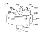
- FIG. 2 is a perspective view of the first polishing unit.
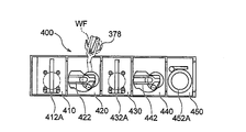
- FIG. 3A is a plan view of the cleaning unit.
- FIG. 3B is a side view of the cleaning unit.
- FIG. 4 is a block diagram of the polishing equipment system.
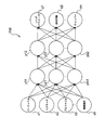
- FIG. 5 is a block diagram showing a neural network used for updating the database.
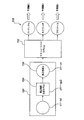
- FIG. 6 is a block diagram showing a neural network and a simulation model used for updating the database.
- FIG. 7 is a block diagram showing a neural network and a simulation model used for updating the database.
- FIG. 8 is a block diagram showing a neural network and a simulation model used for updating the database.
- FIG. 9 is a block diagram showing a neural network and a simulation model used for updating the database.
- the control system for controlling the polishing apparatus for polishing the substrate can be arranged in the polishing apparatus as a part of the polishing apparatus. Further, the control system can be arranged outside the polishing device as a device outside the polishing device. Further, one control system may control a plurality of polishing devices.
- the outline of the polishing apparatus will be described first. After that, a polishing device system that controls a plurality of polishing devices with one control system will be described.
- FIG. 1 is a plan view of the polishing apparatus.
- the polishing apparatus 1000 includes an EFEM (Equipment Front End Module) 200, a polishing unit 300, and a cleaning unit 400. Further, the polishing device 1000 includes a control unit 500 for controlling various operations of the EFEM 200, the polishing unit 300, and the cleaning unit 400.
- EFEM Equipment Front End Module
- the polishing unit 300 is a polishing unit configured to polish the substrate.
- the cleaning unit 400 is a cleaning unit configured to clean the polished substrate.
- the EFEM200 is configured to transport the substrate in the carrier, which is a container for storing and transporting a plurality of substrates, into the polishing apparatus 1000, and to transport the processed substrate from the polishing apparatus 1000 to the carrier. It is a department. Hereinafter, the EFEM 200, the polishing unit 300, and the cleaning unit 400 will be described.
- the EFEM 200 is a unit for passing the substrate before the treatment such as polishing and cleaning to the polishing unit 300 and receiving the substrate after the treatment such as polishing and cleaning from the cleaning unit 400.
- the EFEM200 includes a plurality of (four in this embodiment) front load portions 220.
- a cassette 222 for stocking a substrate is mounted on each of the front load portions 220.
- the EFEM 200 includes a rail 230 installed inside the housing 100, and a plurality of (two in this embodiment) transfer robots 240 arranged on the rail 230.
- the transfer robot 240 takes out the substrate before the processing such as polishing and cleaning from the cassette 222 and hands it to the polishing unit 300. Further, the transfer robot 240 receives the substrate after the processing such as polishing and cleaning from the cleaning unit 400 and returns it to the cassette 222.
- the polishing unit 300 is a unit for polishing a substrate.
- the polishing unit 300 includes a first polishing unit 300A, a second polishing unit 300B, a third polishing unit 300C, and a fourth polishing unit 300D.
- the first polishing unit 300A, the second polishing unit 300B, the third polishing unit 300C, and the fourth polishing unit 300D have the same configuration as each other. Therefore, only the first polishing unit 300A will be described below.
- the first polishing unit 300A includes a polishing table 320A and a top ring 330A.
- the polishing table 320A is rotationally driven by a drive source (not shown).
- a polishing pad 310A is attached to the polishing table 320A.
- the top ring 330A holds the substrate and presses against the polishing pad 310A.
- the top ring 330A is rotationally driven by a drive source (not shown).
- the substrate is polished by being held by the top ring 330A and pressed against the polishing pad 310A.
- the transport mechanism includes a lifter 370, a first linear transporter 372, a swing transporter 374, a second linear transporter 376, and a temporary stand 378.
- the lifter 370 receives the board from the transfer robot 240.
- the first linear transporter 372 transports the substrate received from the lifter 370 between the first transport position TP1, the second transport position TP2, the third transport position TP3, and the fourth transport position TP4.
- the first polishing unit 300A and the second polishing unit 300B receive the substrate from the first linear transporter 372 and polish it.
- the first polishing unit 300A and the second polishing unit 300B pass the polished substrate to the first linear transporter 372.
- the swing transporter 374 transfers the substrate between the first linear transporter 372 and the second linear transporter 376.
- the second linear transporter 376 transports the substrate received from the swing transporter 374 between the fifth transport position TP5, the sixth transport position TP6, and the seventh transport position TP7.
- the third polishing unit 300C and the fourth polishing unit 300D receive the substrate from the second linear transporter 372 and polish it.
- the third polishing unit 300C and the fourth polishing unit 300D pass the polished substrate to the second linear transporter 372.
- the substrate that has been polished by the polishing unit 300 is placed on the temporary storage table 378 by the swing transporter 374.
- the cleaning unit 400 is a unit for cleaning and drying the substrate that has been polished by the polishing unit 300.
- the cleaning unit 400 includes a first cleaning chamber 410, a first transport chamber 420, a second cleaning chamber 430, a second transport chamber 440, and a drying chamber 450.
- the substrate placed on the temporary storage table 378 is transported to the first cleaning chamber 410 or the second cleaning chamber 430 via the first transport chamber 420.
- the substrate is cleaned in the first cleaning chamber 410 or the second cleaning chamber 430.
- the substrate cleaned in the first cleaning chamber 410 or the second cleaning chamber 430 is transported to the drying chamber 450 via the second transport chamber 440.
- the substrate is dried in the drying chamber 450.
- the dried substrate is taken out from the drying chamber 450 by the transfer robot 240 and returned to the cassette 222.
- FIG. 2 is a perspective view of the first polishing unit 300A.
- the first polishing unit 300A includes a polishing liquid supply nozzle 340A for supplying a polishing liquid or a dressing liquid to the polishing pad 310A.
- the polishing liquid is, for example, a slurry.
- the dressing liquid is, for example, pure water.
- the first polishing unit 300A includes a dresser 350A for conditioning the polishing pad 310A.
- the first polishing unit 300A includes an atomizer 360A for injecting a liquid or a mixed fluid of a liquid and a gas toward the polishing pad 310A.
- the liquid is, for example, pure water.
- the gas is, for example, nitrogen gas.
- the top ring 330A is supported by the top ring shaft 332A.
- the top ring 330A is rotated about the axis of the top ring shaft 332A by a drive unit (not shown) as shown by an arrow AB.
- the polishing table 320A is supported by the table shaft 322A.
- the polishing table 320A is rotated about the axis of the table shaft 322A by a drive unit (not shown) as shown by an arrow AC.
- the substrate WF is held by vacuum suction on the surface of the top ring 330A facing the polishing pad 310A.
- the polishing liquid is supplied from the polishing liquid supply nozzle 340A to the polishing surface of the polishing pad 310A.
- the polishing table 320A and the top ring 330A are rotationally driven.
- the substrate WF is polished by being pressed against the polished surface of the polishing pad 310A by the top ring 330A.
- FIG. 3A is a plan view of the cleaning unit 400.
- FIG. 3B is a side view of the cleaning unit 400.
- a support shaft 424 extending in the vertical direction and a first transport robot 422 movably supported by the support shaft 424 are arranged.
- the first transfer robot 422 can be moved in the vertical direction along the support shaft 424 by a drive mechanism such as a motor.
- the first transfer robot 422 receives the substrate WF placed on the temporary storage table 378.
- the first transfer robot 422 transfers the substrate WF received from the temporary storage table 378 to the first cleaning chamber 410 or the second cleaning chamber 430.
- the upper primary cleaning module 412A and the lower primary cleaning module 412B are arranged along the vertical direction.
- the upper secondary cleaning module 432A and the lower secondary cleaning module 432B are arranged along the vertical direction.
- the upper primary cleaning module 412A, the lower primary cleaning module 412B, the upper secondary cleaning module 432A, and the lower secondary cleaning module 432B are cleaning machines that clean the substrate using a cleaning liquid.
- a temporary board 434 is provided between the upper secondary cleaning module 432A and the lower secondary cleaning module 432B.
- the first transfer robot 422 is placed between the temporary storage table 378, the upper primary cleaning module 412A, the lower primary cleaning module 412B, the temporary storage table 434, the upper secondary cleaning module 432A, and the lower secondary cleaning module 432B.
- the substrate WF can be conveyed.
- the first transfer robot 422 has an upper hand and a lower hand. Since the slurry is attached to the substrate before cleaning, the first transfer robot 422 uses the lower hand when conveying the substrate before cleaning. On the other hand, the first transfer robot 422 uses the upper hand when transferring the washed substrate.
- a support shaft 444 extending in the vertical direction and a second transport robot 442 movably supported by the support shaft 444 are arranged.
- the second transfer robot 442 can be moved in the vertical direction along the support shaft 444 by a drive mechanism such as a motor.
- the second transfer robot 442 receives the substrate WF from the second cleaning chamber 430 and conveys it to the drying chamber 450.
- the upper drying module 452A and the lower drying module 452B are arranged along the vertical direction.
- the upper drying module 452A includes a drying unit 456A for drying the substrate WF, and a fan filter unit 454A for supplying clean air to the drying unit 456A.
- the lower drying module 452B includes a drying unit 456B for drying the substrate WF, and a fan filter unit 454B for supplying clean air to the drying unit 456B.
- the second transfer robot 442 can transfer the substrate WF between the upper secondary cleaning module 432A, the lower secondary cleaning module 432B, the temporary stand 434, the upper drying module 452A, and the lower drying module 452B. It can. Since the second transfer robot 442 transfers the washed substrate, it has only one hand.
- the substrate WF is dried from the drying chamber 450 by the upper hand of the transfer robot 240 shown in FIG. 1 after being dried by the upper drying module 452A or the lower drying module 452B.
- the transfer robot 240 returns the substrate WF taken out from the drying chamber 450 to the cassette 222.
- the polishing device system 101 includes a control system 102 and a plurality of polishing devices 1000.
- the plurality of polishing devices 1000 are arranged on a plurality of production lines 104-1, 104-2, ..., 104-N.
- a plurality of semiconductor manufacturing equipment such as an exposure apparatus, a dry etching apparatus, a CVD apparatus, and a polishing apparatus 1000 are arranged in each of the production lines 104-1, 104-2, ..., 104-N. In FIG. 4, only the polishing apparatus 1000 is shown. Other semiconductor manufacturing equipment is omitted.
- the plurality of polishing devices 1000 are referred to as polishing device group 108.
- the control system 102 is a yield improving system that controls the polishing device 1000 to improve the yield in polishing the substrate by the polishing device 1000 to improve the yield.
- one control system 102 controls a plurality of polishing devices 1000.
- the control system 102 may be arranged for each polishing device 1000.
- the control system 102 may be arranged in a computer installed outside the factory where the polishing apparatus group 108 and the inspection apparatus group 110 are arranged.
- a cloud or the like is also possible.
- the computer is connected to the polishing device group 108 and the inspection device group 110 by communication means such as the Internet or a dedicated line.
- the plurality of polishing devices 1000 are not limited to those having the same configuration and function, but may have different configurations and functions.
- a polishing device 1000 suitable for polishing a metal film and a polishing device 1000 suitable for polishing an insulating film may be arranged.
- the polishing apparatus 1000 is provided with a number indicating a serial number of the production line 104 and a serial number in the production line 104 as "N-2".
- a plurality of inspection devices 106 for inspecting the substrate are arranged on each production line 104-1, 104-2, ..., 104-N.
- the inspection device 106 checks for defects in the substrate and the like in light of a predetermined standard. Defects include dust, foreign matter, scratches, broken circuits, and excess or deficiency of film thickness.
- the inspection device 106 includes an SEM type inspection device, an optical inspection device, a film thickness inspection device, and the like.
- the plurality of inspection devices 106 are not limited to those having the same configuration and function, but may have different configurations and functions.
- a number indicating a serial number of the production line 104 and a serial number in the production line 104 are attached to the inspection device 106 as "N-2".
- one inspection device 106 corresponds to one polishing device 1000, and the substrate can be inspected before and after polishing or during polishing.
- one inspection device 106 corresponds to a plurality of polishing devices 1000, and the substrate to be processed by the plurality of polishing devices 1000 is inspected.
- a plurality of inspection devices 106 may correspond to one polishing device 1000, and a plurality of inspection devices 106 may inspect the substrate processed by the one polishing device 1000.
- the inspection device 106 may be used in a process other than the polishing process by the polishing device 1000.
- the polishing device 1000 also has a film thickness sensor, measures the film thickness, and when there is an abnormality in the film thickness, the defect data receiving unit 112 informs that there is a defect via the signal line 122. Send.
- each production line 104-1, 104-2, ..., 104-N has the same number of polishing devices 1000 and the same number of inspection devices 106, that is, N polishing devices 1000 and M polishing devices. It is said that there is an inspection device 106. However, the number of polishing devices 1000 and the number of inspection devices 106 in each production line 104 may differ for each production line 104.
- the plurality of inspection devices 106 are referred to as inspection device group 110.
- the control system 102 includes a defect data receiving unit 112 configured to receive defect data related to substrate defects, and a processing data receiving unit 114 configured to receive processing data related to the processing content of the substrate in the polishing apparatus. Based on the defect data and the processing data, the defect occurrence cause identification unit 116 configured to identify the defect occurrence cause and the defect correction action for correcting the defect for the identified occurrence cause are determined. It has a defect correction treatment unit 118 configured to instruct defect correction treatment to at least one of the polishing unit, the cleaning unit, and the transport unit.
- the control system 102 further receives treatment result data regarding the result of the defect correction treatment after at least one of the polishing unit, the cleaning unit, and the transport unit has executed the defect correction treatment, and the control system 102 receives the treatment result data regarding the result of the defect correction treatment, and the defect is based on the treatment result data. It has a database update unit 142 (action result data processing unit) capable of changing corrective actions.
- the defect data receiving unit 112, the processing data receiving unit 114, the defect occurrence cause identification unit 116, the defect corrective action unit 118, and the database update unit 142 receive instructions from the control unit 146 as described later, respectively. Perform the processing of.
- the defect data receiving unit 112, the processing data receiving unit 114, the defect occurrence cause identification unit 116, the defect corrective action unit 118, and the database update unit 142 signal each other without receiving instructions from the control unit 146. May be exchanged so that they operate in the order described later.
- Each of the above units of the control system 102 is controlled by the control unit 146 so as to repeat the following flow. That is, the control unit 146 sends an instruction to the defect data receiving unit 112 via the a) signal line 148, receives the defect data related to the defect from the inspection device group 110, and collects the defect information.
- the defect data receiving unit 112 receives all the inspection data from the inspection apparatus group 110, and if the inspection data includes information indicating a defect, the defect data receiving unit 112 processes the inspection data as defect data.
- the defect data receiving unit 112 may receive only the defect data from the inspection device group 110. When the defect data receiving unit 112 receives the defect data, the defect data receiving unit 112 transmits to that effect to the control unit 146 via the signal line 148.
- the inspection data means data obtained by inspecting the substrate by the inspection apparatus group 110.
- an instruction is sent to the processing data receiving unit 114 via the signal line 148, and the processing data receiving unit 114 is made to receive processing data related to the processing content of the substrate in the polishing apparatus to collect production information.
- the processing data receiving unit 114 may receive the processing data regarding the processing content of the substrate only for the polishing apparatus 1000 in which the defect has occurred, and the processing data regarding the processing content of the substrate may be received for all the polishing apparatus 1000. You may receive it.
- the defect data receiving unit 112 when the defect data receiving unit 112 receives the defect data from the inspection device group 110, it sends an instruction to the defect occurrence cause identification unit 116 via the signal line 148 to identify the defect occurrence cause. When the defect data receiving unit 112 does not receive the defect data from the inspection device group 110, the process returns to step a).
- an instruction is sent to the defect corrective action unit 118 via the signal line 148 to determine the defect corrective action for correcting the defect for the identified cause, and the polishing unit, the cleaning unit, and the transport unit are used. Have at least one of them instruct defect corrective action. At least one of the polishing part, the cleaning part and the conveying part takes defect correction measures according to the instructions.
- an instruction is sent to the defect data receiving unit 112 via the signal line 148 to receive the inspection data from the inspection device group 110.
- an instruction is sent to the processing data receiving unit 114 via the signal line 148, the processing data receiving unit 114 is made to receive the processing data regarding the processing content of the substrate in the polishing apparatus, and the production information is collected.
- an instruction is sent to the database update unit 142 via the signal line 148 to receive the treatment result data (received inspection data and processing data) regarding the result of the defect correction treatment, and the defect correction is performed based on the treatment result data. Change the procedure. In this way, corrective action is implemented and the effect is measured after implementation. Then, the process returns to step a), and steps a) to e) are repeated.
- step e) if the obtained treatment result data matches the previous treatment result data stored in the defect knowledge database 144 within a predetermined range, the database update unit 142 has a defect in the defect knowledge database 144. Do not change corrective action. If the obtained action result data does not match the previous action result data within a predetermined range and is improved, the database update unit 142 changes the defect corrective action in the defect knowledge database 144.
- the database update unit 142 sends an alarm to the control unit 146 when the obtained treatment result data does not match the previous treatment result data within a predetermined range and is deteriorated.
- the control unit 146 further sends an alarm to the control unit 500 or the host computer 126.
- control system 102 controls each part of the polishing device 1000 via the control unit 500. And defect corrective action can be taken.
- each polishing device 1000 controls the operation of a main controller (control unit 500) that controls each polishing device 1000 and each unit (EFEM 200, polishing unit 300, cleaning unit 400, etc.) of each polishing device 1000. It may have a plurality of unit controllers.
- the main controller and the unit controller each have a CPU, a memory, a recording medium, and software stored in the recording medium for operating each unit.
- the control system 102 includes a CPU, a memory, a recording medium, software recorded on the recording medium, and the like.
- the control system 102 monitors and controls defects in the entire polishing apparatus 1000, and performs signal transmission / reception, information recording, and calculation for that purpose.
- the software is updatable.
- the software does not have to be updatable.
- the defect data receiving unit 112 transmits defect data (information on substrate lot information, defects, processing conditions, etc.) from the inspection device group 110, the polishing device group 108, and the host computer 126 to the signal line 120, the signal line 122, and the signal, respectively. Receive via line 128. From the inspection device group 110, lot information of the substrate and data related to defects (dust, scratches, etc.) are transmitted via the signal line 120. From the polishing device group 108, data on lot information of the substrate and data on defects (identification number of the polishing device 1000, processing conditions, film thickness outside the specified value, etc.) are transmitted via the signal line 122.
- the number of signal lines 120 and 122 may be the same as the number corresponding to the inspection device 106 and the polishing device 1000. Further, the signal line 120 and the signal line 122 may transmit data by time division multiplexing, and the number of the signal line 120 and the signal line 122 may be smaller than the total number of the inspection device 106 and the polishing device 1000.
- the lot information of the substrate regarding the defects generated in the substrate in the manufacturing process before the manufacturing process shown in FIG. 4 and the data related to the defects (dust, scratches, etc., and whether or not the defects can be corrected by the polishing device 1000) are signals. It is transmitted to the defective data receiving unit 112 via the line 128.
- the defect data receiving unit 112 sends the received defect data to the defect database 124 via the signal line 130.
- the defect database 124 accumulates defect data received from the defect data receiving unit 112 for each manufacturing line 104.
- the defect data received by the defect data receiving unit 112 is as follows. From the inspection device group 110, the defect data receiving unit 112 provides lot information of the defective substrate, and in the case of particles (foreign matter) as defect information, data such as the number, size, and color of the particles, and scratches (scratches). In the case of, the number, size, depth, part (distance from the center of the substrate), etc. of scratches (scratches) are received. The defect data receiving unit 112 receives the lot information of the defective substrate and the maximum and minimum values of the film thickness distribution or the film thickness as the defect information from the polishing apparatus group 108.
- the defect data receiving unit 112 also receives the same data from the host computer 126 as defect information in another process. That is, lot information of the defective substrate, data such as the number, size, and color of particles in the case of particles (foreign matter) as defect information, and the number and size of scratches (scratches) in the case of scratches (scratches). , Depth, site (distance from the center of the substrate), film thickness distribution or maximum and minimum values of film thickness, etc. are received.
- the processing data receiving unit 114 receives processing data regarding the processing content of the substrate in the polishing apparatus 1000 (lot information of the substrate, information of the polishing apparatus 1000 that generated defects (process data, alarm history, history information of consumable members in the polishing apparatus 1000). Etc.)) is received from the polishing apparatus group 108 via the signal line 132.
- the processing data receiving unit 114 sends the received processing data to the polishing database 136 via the signal line 134.
- the polishing database 136 accumulates the processing data received from the processing data receiving unit 114 for each production line 104.
- the processing data received by the processing data receiving unit 114 is as follows. a) As information about the processing lot, lot information of the substrate, contents of each processing recipe of transfer / polishing / cleaning, (here, the processing recipe is given to each part of the polishing apparatus 1000 when processing the substrate. It is, for example, a list format that describes the instructions, procedures, settings, parameters, etc. that are to be used.) B) How to actually use the recipe assigned to each process of transport route and polishing / cleaning as process data. A log that can determine whether processing has been performed, c) A log that records all the occurrence / cancellation of alarms of each polishing device 1000, ON / OFF of contacts with time, and all process data in the device at predetermined time intervals. d) In order to guarantee the quality of each polishing device 1000, data that determines the variation in processing results from the rising and falling times of various data during substrate processing and the standard deviation of process data, e) Use of consumable parts Time etc.
- the defect database 124 and the polishing database 136 transmit defect data and processing data to the database update unit 142 via the signal line 138 and the signal line 140, respectively.
- the database update unit 142 stores the received defect data and processing data in the defect knowledge database 144.
- the defect knowledge database 144 contains defect data detected by the inspection device group 110 in the polishing process, defects detected in other than the polishing process and within a range that can be dealt with by the polishing device 1000, and detected by the polishing device group 108. Accumulate the processed data.
- the defects detected outside the polishing step are defect data and processing data transmitted from the host computer 126 to the defect data receiving unit 112 via the signal line 128.
- the defect knowledge database 144 has data showing the correspondence between the defect data and the processing data, the cause of the defect, and the defect corrective action.
- the correspondence between the newly added defect data and processing data, the cause of the defect, and the defect corrective action is updated by the database update unit 142 as follows. This will be described with reference to FIGS. 5 to 10.
- the database update unit 142 can determine the cause of the defect and the defect corrective action by using any method such as a decision tree, a neural network, or a simulation in order to obtain a correspondence relationship.
- FIG. 5 shows an example using a neural network.
- Figures 6 to 10 show an example using simulation. These are sample models, and the embodiments of the present invention are not limited thereto.
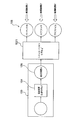
- FIG. 5 is a block diagram showing a neural network 150 used for updating the database.
- the neural network 150 is implemented as a computer program that executes AI (artificial intelligence). A part of the neural network 150 may be implemented as hardware.
- the neural network 150 performs automatic learning, and specifically, machine learning may be performed, and deep learning may be performed as machine learning. Learning data (defect data and processing data) is input to the neural network 150, and the neural network 150 outputs output data (defect occurrence cause and defect correction treatment).
- the neural network 150 after learning by the neural network 150 is used in the actual polishing process.
- the neural network 150 is input with learning data created from the data obtained in the actual polishing process, and outputs the above-mentioned output data (defect occurrence cause and defect corrective action).
- FIG. 5 is a diagram showing a configuration example of the neural network 150.
- the neural network 150 has an input layer including neurons (input nodes) x1, x2, x3, ..., Xl that input input data (defect data and processed data).
- the neural network 150 includes m neurons y11, y21, y31, ..., ym1 (hidden node) and p neurons y12, y22, y32, ..., Yp2 (yp2) that connect the input node and the output node. It has an intermediate layer (hidden layer) including a hidden node).
- the neural network 150 has an output layer including n neurons z1, z2, z3, ..., Zn (output nodes) that output the cause of the defect and the defect corrective action. Although only two intermediate layers are shown in this figure, one or three or more intermediate layers may be provided.
- the neural network 150 may learn failure prediction according to machine learning (called deep learning or deep learning) by a multi-layer (four or more layers) neural network (deep neural network), for example.
- This figure is a 4-layer neural network (deep neural network).
- the neural network 150 learns the normal / abnormal polishing of the polishing unit.
- the neural network 150 processes defect data and processing by so-called "supervised learning” according to a data set created based on a combination of defect data, normal data, and processing data acquired by the inspection device group 110 and the polishing device group 108. Learn the relationship between the data and the causes of defects and defect corrective actions.
- "supervised learning” is a model in which a large number of sets of data of a certain input and a result (label) are given to a learning device to learn the features in those data sets and estimate the result from the input. That is, the relationship can be acquired inductively.
- the neural network can accumulate only state variables in a state without abnormality, that is, when the polishing unit is operating normally, and can learn normal / abnormal polishing by so-called “unsupervised learning”. ..
- “unsupervised learning” means that by giving a large amount of input data to the neural network 150, it is possible to learn how the input data is distributed, and even if the corresponding teacher output data is not given. It is a method to learn to perform compression, classification, shaping, etc. on input data. The features in those datasets can be clustered among similar people. By using this result and assigning an output that optimizes it by setting some standard, normal / abnormal judgment can be realized.
- input data related to particles, scratches, profile abnormalities, and device abnormalities are input to neurons x1, x2, x3, ..., Xl, respectively.
- one input data for each particle, scratch, profile abnormality, and equipment abnormality is input, but this is an example, and two or more input data for particles, scratch, profile abnormality, and equipment abnormality are input. You may. Further, input data other than input data related to particles, scratches, profile abnormalities, and device abnormalities may be input.
- Neurons z1, z2, z3, ..., Zn output output data related to recipes (that is, parameters, etc.), member replacement procedures, and unit stop, respectively.
- recipes that is, parameters, etc.
- member replacement procedures that is, parameters, etc.
- unit stop a unit stop for the recipe, the member replacement procedure, and the unit stop.
- output data other than the output data related to the recipe, the member replacement procedure, and the stop of the unit may be output.
- the number of rough defect types of input nodes and the number of corrective action nodes of output nodes may not be increased. However, even in this case, the number of input nodes and / or output nodes may be added or changed from the control server (in the same row as the host computer 126) above the host computer 126 and the polishing apparatus 1000.
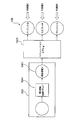
- FIGS. 6 to 9 are block diagrams showing a neural network and a simulation model used for updating the database.
- the procedure of FIGS. 6 to 9 improves the defect correction measures and improves the accuracy of the neural network 150.
- the initial forms of the neural network 150 and the simulation model g152 may be prepared in advance, or may be specified and / or updated by the host computer 126.
- FIG. 6 is a diagram showing a simulation result when polishing is performed according to the corrective measures z1 to zn obtained by the neural network 150 before performing the corrected polishing.
- the simulation results are obtained by inputting corrective actions z1 to zn into the simulation model g152.
- the intermediate layer containing the m neurons y11, y21, y31, ..., Ym1 and p neurons y12, y22, y32, ..., Yp2 in FIG. 5 is referred to as a corrective action generation model f154. ..
- the output layer containing n neurons z1, z2, z3, ..., Zn in FIG. 5 is referred to as corrective action 156.
- the simulation model g152 is input with the corrective action 156, and outputs the inspection data (or defect data) after polishing and the processing data as the simulation result 158.
- a multivariable input / multivariable output function, a neural network, or the like can be used.
- What is output as the simulation result 158 is the defect data described above. That is, it is data showing information on defects in the substrate. However, since the simulation result 158 is obtained as a result of corrective action, the simulation result 158 may be a normal value. In this figure, one simulation result 158 for each of particles, scratches, and profile abnormalities is output as the simulation result 158.
- one simulation result 158 for each of particles, scratches, and profile abnormalities is output.
- two or more simulation results 158 regarding particles, scratches, and profile abnormalities may be output.
- a simulation result 158 other than the simulation result 158 relating to particles, scratches, and profile abnormalities may be output.
- the simulation results 158 relating to particles, scratches, and profile abnormalities are referred to as predicted value C, predicted value D, and predicted value E, respectively.
- the predicted value C, the predicted value D, and the predicted value E all have values that satisfy the specification values and the acceptance criteria at this stage.
- the simulation model g152 is improved by the measured values obtained by actual polishing.
- the improved simulation model g152 will be referred to as the simulation model g'1521. This is shown in FIG.
- a processing result C', a processing result D', and a processing result E'that are different from the predicted value C, the predicted value D, and the predicted value E are obtained, the processing result C is used by using the corrective action x156 shown in FIG.
- the simulation model g152 is improved so that', processing result D', and processing result E'are obtained.
- the acceptance reference values C, D, and E that is, the predicted value C, the predicted value D, and the predicted value E
- a corrective action x'1561 that can obtain the passing standard values C, D, and E using the improved simulation model g'1521 is obtained.
- the method of obtaining the corrective action x'1561 that can obtain the passing reference values C, D, and E using the simulation model g'1521 is to solve the equation when the simulation model g'1521 is a function.
- the simulation model g'1521 is a neural network
- the method of obtaining the corrective action x'1561 is to use the dummy input data until the passing reference values C, D, and E can be obtained. It is to repeat learning.
- the learning of neural networks is to correct the weights and biases of neurons in neural networks by the backpropagation method.
- the corrective action generation model f154 is improved so that the corrective action x'1561 is obtained, and the improved corrective action generation model f'1541 is obtained.
- the method of obtaining the corrective action generation model f'1541 that can obtain the corrective action x'1561 using the corrective action x'1561 uses dummy input data until the corrective action x'1561 can be obtained.
- the corrective action generation model f154 is to repeat learning as AI.
- the learning of neural networks is to correct the weights and biases of neurons in neural networks by the backpropagation method. In this way, the corrective action generation model f'1541 capable of generating the corrective action x'1561 is obtained.
- FIGS. 6 to 8 are examples of methods for improving the corrective action generation model f154. It may be improved (learned) by other methods. For example, in the method shown in FIG. 8, a corrective action generation model is used by using the respective ideal values C'', D'', E'' and the simulation model g'1521 instead of the acceptance reference values C, D, and E.
- the corrective action generation model f''1542 may be obtained by learning f154. This is shown in FIG. Corrective action x ′′ 1562 can be obtained by the corrective action generation model f ′′ 1542.
- the cause of the defect and the corrective action for the defect are determined by using the neural network 150 and the simulation.
- the simulation model 150' may be used instead of the neural network 150 to obtain corrective actions z1 to zn. That is, the simulation model 150'and the simulation model g152 may be used.
- the simulation result 158 is obtained by inputting the corrective actions z1 to zn obtained by the simulation model 150'to the simulation model g152.
- the defect occurrence cause identification unit 116 accesses the defect knowledge database 144, identifies the defect occurrence cause with respect to the newly added defect data and the processing data indicating the defect, and determines the defect correction action unit. Output to 118.
- the data output by the defect occurrence cause identification unit 116 includes lot information of the substrate on which the defect has occurred, the polishing apparatus 1000 that generated the defect, and the unit in the polishing apparatus 1000 that generated the defect (sometimes referred to as a "chamber"). Identification information, cause of defect occurrence (part that generated the defect and / or processing content), etc. Factors that have generated defects include equipment failure and / or equipment malfunction and / or equipment setting error and / or device processing improperness.
- the defect corrective action unit 118 accesses the defect knowledge database 144 for the input defect occurrence cause, and determines the defect corrective action for correcting the defect.
- the defect knowledge database 144 stores defect corrective actions corresponding to the causes of defects. After that, the defect corrective action unit 118 instructs at least one of the polishing unit 300, the cleaning unit 400, and the EFEM 200 to take corrective action.
- the defects to be corrected are the defects generated by the polishing device 1000 and the defects that can be dealt with by the polishing device 1000.
- the data output by the defect corrective action unit 118 is the polishing device 1000 identification information, the unit identification information in the polishing device 1000, and the specific corrective action.
- Corrective actions include a) unit stop, b) processing recipe change (tuning of each parameter, transfer route change, etc.), c) polishing device setting constant (parameter) change (related to the operation of the polishing device in addition to the processing recipe). If there is a parameter) etc.
- the specific corrective measures corresponding to the cause of the defect are as follows, for example. 1. 1.
- corrective action is taken.
- the number of particles increases and the number of particles exceeds the reference value, the corresponding cleaning module in the cleaning unit 400 is stopped so that the transport route using the cleaning module cannot be used. This will be described.
- the four polishing units in the polishing device 1000 are a pair of two first polishing units 300A and a second polishing unit 300B on the right side of FIG. 1 and two third polishing units 300C and a fourth polishing unit 300D on the left side.
- the two polishing units on the right are combined, for example, with the cleaning module on the top.
- the two polishing units on the left side are combined with the cleaning module on the lower side.
- the typical transportation route is as follows. Upper route: 1st polishing unit 300A ⁇ 2nd polishing unit 300B ⁇ Upper primary cleaning module 412A ⁇ Upper secondary cleaning module 432A ⁇ Upper drying module 452A Lower route: 3rd polishing unit 300C ⁇ 4th polishing unit 300D ⁇ Lower side Primary cleaning module 412B ⁇ Lower secondary cleaning module 432B ⁇ Lower drying module 452B
- an example of stopping the cleaning module determined to be defective and disabling the transport route using the cleaning module is as follows. For example, if it is determined that there is an abnormality in the upper primary cleaning module 412A, corrective measures such as stopping the upper primary cleaning module 412A and using the lower route are adopted.
- the polishing unit is stopped so that the transfer route using the polishing unit cannot be used.
- An example of this is as follows. For example, when it is determined that there is an abnormality in the first polishing unit 300A, the first polishing unit 300A and the second polishing unit 300B are stopped, and polishing is performed by the third polishing unit 300C and the fourth polishing unit 300D. Adopt corrective action.
- the following corrective measures will be taken. That is, in the inspection after cleaning with the cleaning unit 400, when the amount of particles tends to increase, it is presumed that insufficient cleaning is the cause of the defect, and (1) the cleaning recipe is changed for cleaning. Increase time and / or chemical flow rate. (2) One or more corrections of the deviation of the chemical solution supply point (dropping on the wafer is not in the predetermined position) are judged as defect correction measures. If (2) is taken as a corrective measure, a correction chemical supply position fraud alarm is issued, the corresponding cleaning module is stopped, and a transport route that does not go through the relevant module is set so that the maintenance staff can correct the chemical solution supply point. Instruct to use.
- the particle map data showing the distribution state of the particles
- the roll member is the cause of the defect.
- (1) replacement of the roll member (2) adjustment of the self-cleaning condition of the roll member (adjustment of the cleaning time of the roll member and the pressing load of the roll member against the self-cleaning plate), (3) self-cleaning of the roll member.
- One or more of the cleaning plate replacements (because there is a possibility of back-contamination from the self-cleaning plate to the roll member) is judged as a defect correction measure.
- the self-cleaning of the roll member is a cleaning process of the roll member itself.
- the self-cleaning of the roll member is performed by cleaning the roll member in the cleaning unit 400 using a self-cleaning plate instead of the wafer.
- the self-cleaning of the pen member which will be described later, is a cleaning process of the pen member itself, and the self-cleaning of the pen member is also performed in the same manner.
- the roll member is a component for cleaning the substrate WF.
- the roll member is attached to the rotating shaft in the cleaning module.
- the roll member is a sponge arranged on a cylinder (rotational shaft).
- the inspection devices included in the inspection device group 110 include a wafer surface inspection device, a defect inspection device, and the like, as described above. These are generally called inspection devices in the field of semiconductor manufacturing.
- the particle map is caused by the shape of the pen member in the inspection by the inspection device group 110
- the pen member is the cause of the defect.
- (1) replacement of the pen member (2) adjustment of the self-cleaning condition of the pen member (adjustment of the cleaning time and pressing load of the pen member), (3) replacement of the self-cleaning plate of the pen member (from the self-cleaning plate).
- One or more of (because there is a possibility of reverse contamination of the pen member) is judged as a defect correction measure.
- the pen member is a component for cleaning the substrate WF.
- the pen member is attached to a rotating shaft within the cleaning module.
- the pen member is a sponge arranged at the tip of the rotating shaft.
- the cleaning module in which the roll member is arranged and the cleaning module in which the pen member is arranged are usually separate cleaning modules.
- the number of particles is increasing, but when the cause cannot be identified, the following cause identification measures are taken as defect correction measures. That is, all the polishing units 300 and the cleaning unit 400 that have processed the wafer WF whose particles tend to increase are transported so that the processing is performed only by the unit for each unit.
- the unit that is the source is identified by re-inspecting all the processed wafers with the inspection apparatus group 110. Instruct the execution of such a cause isolation test.
- the transport recipe is changed, the route does not go through the corresponding unit, and the defect corrective action to stop the corresponding unit is instructed. To do.
- the polishing unit 300 In the inspection by the inspection device, when the scratch has a long shape on the wafer surface, the solid matter on the polishing table (diamond or slurry solid matter of the dresser disk) is the cause of the defect, so the polishing unit 300 The cleaning sequence is interrupted, pad cleaning (cleaning with an atomizer and dressing treatment) is performed, and defect correction measures are instructed to wash away the solid matter on the polishing table.
- the pressure to press the wafer onto the pad is too strong in the water poly (polishing using only pure water) step performed before the completion of polishing, and the slurry attached to the wafer is sufficiently removed. It is thought that the cause is not so good.
- the pressure for pressing the wafer against the pad is checked, and a defect correction measure for reducing the pressure within the range of the reference value allowed by the host computer 126 is instructed.
- each polishing unit 300 is transported so that the processing is performed only by the polishing unit 300. After that, all the used wafers are re-inspected by the inspection apparatus group 110 to identify the polishing unit 300 as the source. Instruct the execution of such a cause isolation test.
- the overprocess time means an offset time for extra polishing after actually detecting a feature point (that is, the end point of polishing). And vice versa. That is, when the amount of polishing is excessive, the polishing time is shortened as a defect correction measure.
- control unit 146 stops the used polishing unit 300.
- the control unit 146 prohibits the use of the transport route using the polishing unit 300.
- the host computer 126 requests the polishing device 1000 to reprocess as a new process (recipe).
- the polishing device 1000 performs the process according to the recipe.
- the coping method at this time is 3. It is the same as the lack of polishing amount shown in the section. That is, the rework treatment (that is, the repolishing and the subsequent cleaning treatment) and other treatments are performed. Perform in the same way as in the section.
- the control unit 146 measures the effect of the corrective action. That is, the control unit 146 sends an instruction to the defect data receiving unit 112, and the treatment result data of the polishing device 1000 related to the cause of occurrence (inspection data received from the inspection device group 110 and processing data received from the polishing device 1000). ) Is received.
- an instruction is sent to the database update unit 142 via the signal line 148 to receive the received action result data regarding the result of the defect corrective action, and to change the defect corrective action based on the action result data.
- the database update unit 142 accesses the defect knowledge database 144 and updates the defect knowledge database 144, if necessary, as described in step e) described above.
- Control unit 100 Housing 101 Polishing device system 102 Control system 104 Manufacturing line 106 Inspection device 108 Polishing device group 110 Inspection device group 112 Defect data receiving unit 114 Processing data receiving unit 116 Defect occurrence cause identification unit 118 Defect correction treatment unit 124 Defect database 126 Host Computer 136 Polishing database 142 Database update unit 144 Defect knowledge database 146 Control unit 200 EFEM 220 Front load part 240 Transfer robot 300 Polishing unit 310A Polishing pad 320A Polishing table 330A Top ring 340A Polishing liquid supply nozzle 350A Dresser 360A Atomizer 370 Lifter 400 Cleaning unit 410 1st cleaning chamber 420 1st transport chamber 422 1st transport robot 430 2 Cleaning chamber 440 Second transport chamber 442 Second transport robot 450 Drying chambers 456A, 456B Drying unit 500 Control unit 1000 Polishing device WF substrate
Landscapes
- Engineering & Computer Science (AREA)
- Mechanical Engineering (AREA)
- Mechanical Treatment Of Semiconductor (AREA)
- Finish Polishing, Edge Sharpening, And Grinding By Specific Grinding Devices (AREA)
- Constituent Portions Of Griding Lathes, Driving, Sensing And Control (AREA)
Abstract
研磨装置を制御するための、歩留まりを改善した制御システム、および研磨方法を提供する。 制御システム102の欠陥データ受信部112は、基板の欠陥に関する欠陥データを受信する。処理データ受信部114は、研磨装置1000における基板の処理内容に関する処理データを受信する。欠陥発生原因特定部116は、欠陥データと、処理データとに基づいて、欠陥の発生原因を特定する。欠陥是正処置部118は、特定された発生原因について欠陥を是正するための欠陥是正処置を決定して、研磨ユニット300と洗浄ユニット400とEFEM200のうちの少なくとも1つに対して、欠陥是正処置を指示する。
Description
本発明は、基板を研磨するための研磨装置を制御するための制御システム、および研磨方法に関するものである。
半導体デバイスの製造では、基板、例えばシリコンウェハの上に多くの種類の材料が膜状に繰り返し形成され、積層構造を形成する。この積層構造を形成するためには、ウェハの表面を平坦にする技術が重要となっている。このようなウェハの表面を平坦化する一手段として、化学機械研磨(CMP)を行う研磨装置(化学的機械的研磨装置ともいう)が広く用いられている。
化学機械研磨(CMP)装置は、一般に、研磨パッドが取り付けられた研磨テーブルと、ウェハを保持するトップリングと、研磨液を研磨パッド上に供給するノズルとを備えている。ノズルから研磨液を研磨パッド上に供給しながら、トップリングによりウェハを研磨パッドに押し付け、さらにトップリングと研磨テーブルとを相対移動させることにより、ウェハを研磨してその表面を平坦にする。CMP装置は、研磨後のウェハを洗浄し、さらに乾燥させる洗浄部を有する。
このような研磨装置においては、基板処理の歩留まりを向上することが求められている。研磨装置は、研磨や洗浄などを行う種々の処理部を有しているため、各処理部での欠陥の発生は、研磨装置全体の歩留まりを低下させてしまう。研磨装置全体の歩留まりは、研磨部や洗浄部などの処理部のみならず、ウェハを搬送する搬送機構(搬送部)にも影響されることがある。このように、研磨装置全体の歩留まりは、種々の処理工程および搬送工程に依存する。
半導体工場で製造中のウェハに欠陥が見つかった場合、欠陥が見つかった工程および、当該工程の上流にある工程に遡って原因を究明する必要がある。原因究明中に欠陥を生み出している可能性がある装置を停止させる時間が長くなると、生産工程に遅れが生じ、生産量の低下につながる。
本発明の一形態は、このような問題点を解消すべくなされたもので、その目的は、研磨装置を制御するための、歩留まりを改善した制御システム、および研磨方法を提供することである。
上記課題を解決するために、形態1では、基板を研磨するための研磨装置を制御するための制御システムにおいて、前記研磨装置は、基板を研磨するように構成された研磨部と、研磨された前記基板を洗浄するように構成された洗浄部と、前記研磨部と前記洗浄部との間で前記基板を搬送するように構成された搬送部とを有し、前記制御システムは、前記基板の欠陥に関する欠陥データを受信するように構成された欠陥データ受信部と、前記研磨装置における前記基板の処理内容に関する処理データを受信するように構成された処理データ受信部と、前記欠陥データと、前記処理データとに基づいて、前記欠陥の発生原因を特定するように構成された欠陥発生原因特定部と、特定された前記発生原因について前記欠陥を是正するための欠陥是正処置を決定して、前記研磨部と前記洗浄部と前記搬送部のうちの少なくとも1つに対して、前記欠陥是正処置を指示するように構成された欠陥是正処置部とを有することを特徴とする制御システムという構成を採っている。
本実施形態では、欠陥データと、処理データとに基づいて、欠陥の発生原因を特定するように構成された欠陥発生原因特定部と、特定された発生原因について欠陥を是正するための欠陥是正処置を決定して、研磨部と洗浄部と搬送部のうちの少なくとも1つに対して、欠陥是正処置を指示するように構成された欠陥是正処置部とを有するため、研磨装置のための、歩留まりを改善した制御システムを提供することができる。
ここで、欠陥データとは、基板の欠陥に関する情報を示すデータである。欠陥データとしては、例えば、欠陥種別(ウェハ上のごみ(以下では「パーティクル」とも呼ぶ。)の有無、ウェハの傷(以下では「スクラッチ」とも呼ぶ。)の有無、研磨不良(以下では「プロファイル異常」とも呼ぶ。)等の欠陥のタイプ)、および欠陥の状態(ごみや傷の数、大きさ、形状、色、位置、分布状態、傷の深さ、研磨の過不足状態を示す量、等)のうちの少なくとも1つである。
処理データとは、基板が研磨装置においてどのような処理を受けたかを示すデータである。処理データとしては、例えば、基板を個々にまたは複数枚単位で識別するためのロット情報、研磨装置内外における各プロセスで基板が受けた処理に関する情報、各プロセスで基板が受けたアラーム情報、基板の処理に用いられた消耗部材情報(研磨パッド等の消耗部材のタイプ、使用時間等)のうちの少なくとも1つである。なお、欠陥データ受信部と処理データ受信部とを1つのデータ受信部としてもよい。すなわち、本発明の1実施形態として、1つのデータ受信部が欠陥データと処理データを受信することとしてもよい。
欠陥是正処置としては、例えば、速やかに欠陥発生原因となっている研磨装置の構成ユニット(研磨部、洗浄部、搬送部等)を停止して、生産ラインから切り離すこと、または欠陥発生原因を解決するように研磨装置の構成ユニットの運転パターン(研磨量の調整、洗浄水の量の調整等)を変更することが可能である。
形態2では、前記研磨部と前記洗浄部と前記搬送部のうちの少なくとも1つが前記欠陥是正処置を実行した後に、前記欠陥是正処置の結果に関する処置結果データを受信して、前記処置結果データに基づいて前記欠陥是正処置を変更することが可能であるように構成された処置結果データ処理部を有することを特徴とする形態1記載の制御システムという構成を採っている。
形態3では、前記欠陥データおよび前記処理データのうちのすくなくとも1つを蓄積するように構成された欠陥知識データベースを有することを特徴とする形態1または2記載の制御システムという構成を採っている。例えば、欠陥があるウェハのロット情報、欠陥種別、欠陥発生原因、欠陥是正処置を互いに関連付けてデータベース化して、蓄積してもよい。これにより、研磨装置の運転方法や、欠陥の発生原因の特定精度を改善することができる。
形態4では、形態1ないし3のいずれか1項に記載の制御システムと、前記研磨部と、前記洗浄部と、前記搬送部とを有することを特徴とする研磨装置という構成を採っている。
形態5では、形態1ないし3のいずれか1項に記載の制御システムと、複数の前記研磨装置とを有することを特徴とする研磨装置システムという構成を採っている。
形態6では、基板を研磨する研磨部と、研磨された前記基板を洗浄する洗浄部と、前記研磨部と前記洗浄部との間で前記基板を搬送する搬送部とを有する研磨装置を用いて、前記基板を研磨する研磨方法において、前記基板の欠陥に関する欠陥データを受信し、前記研磨装置における前記基板の処理内容に関する処理データを受信し、前記欠陥データと、前記処理データとに基づいて、前記欠陥の発生原因を特定し、特定された前記発生原因について前記欠陥を是正するための欠陥是正処置を決定して、前記研磨部と前記洗浄部と前記搬送部のうちの少なくとも1つに対して、前記欠陥是正処置を指示することを特徴とする研磨方法という構成を採っている。
形態7では、前記研磨部と前記洗浄部と前記搬送部のうちの少なくとも1つが前記欠陥是正処置を実行した後に、前記欠陥是正処置の結果に関する処置結果データを受信して、前記処置結果データに基づいて前記欠陥是正処置を変更することを特徴とする形態6記載の研磨方法という構成を採っている。
形態8では、前記欠陥データおよび前記処理データのうちのすくなくとも1つを欠陥知識データベースに蓄積することを特徴とする形態6または7記載の研磨方法という構成を採っている。
以下、本発明の実施形態について図面を参照して説明する。なお、以下の各実施形態において、同一または相当する部材には同一符号を付して重複した説明を省略することがある。また、各実施形態で示される特徴は、互いに矛盾しない限り他の実施形態にも適用可能である。
本発明の実施形態としては、研磨装置が1台のみの場合と、研磨装置が複数台の場合が可能である。また、基板を研磨するための研磨装置を制御するための制御システムは、研磨装置の一部として、研磨装置内に配置することができる。また、制御システムは、研磨装置の外部の装置として、研磨装置の外部に配置することもできる。さらに、1台の制御システムで、複数の研磨装置を制御してもよい。以下では、最初に研磨装置の概要について説明する。その後、1台の制御システムで、複数の研磨装置を制御する研磨装置システムについて説明する。
<研磨装置>
図1は、研磨装置の平面図である。図1に示すように、研磨装置1000は、EFEM(Equipment Front End Module)200と、研磨ユニット300と、洗浄ユニット400と、を備える。また、研磨装置1000は、EFEM200、研磨ユニット300、及び、洗浄ユニット400、の各種動作を制御するための制御ユニット500を備える。
図1は、研磨装置の平面図である。図1に示すように、研磨装置1000は、EFEM(Equipment Front End Module)200と、研磨ユニット300と、洗浄ユニット400と、を備える。また、研磨装置1000は、EFEM200、研磨ユニット300、及び、洗浄ユニット400、の各種動作を制御するための制御ユニット500を備える。
研磨ユニット300は、基板を研磨するように構成された研磨部である。洗浄ユニット400は、研磨された基板を洗浄するように構成された洗浄部である。EFEM200は、基板を複数枚収納して搬送するための容器であるキャリア内の基板を研磨装置1000内へ搬送する処理と処理後の基板を研磨装置1000からキャリアへ搬送するように構成された搬送部である。以下、EFEM200、研磨ユニット300、及び、洗浄ユニット400、について説明する。
<EFEM>
EFEM200は、研磨及び洗浄などの処理が行われる前の基板を研磨ユニット300へ渡すとともに、研磨及び洗浄などの処理が行われた後の基板を洗浄ユニット400から受け取るためのユニットである。EFEM200は、複数(本実施形態では4台)のフロントロード部220を備える。フロントロード部220にはそれぞれ、基板をストックするためのカセット222が搭載される。
EFEM200は、研磨及び洗浄などの処理が行われる前の基板を研磨ユニット300へ渡すとともに、研磨及び洗浄などの処理が行われた後の基板を洗浄ユニット400から受け取るためのユニットである。EFEM200は、複数(本実施形態では4台)のフロントロード部220を備える。フロントロード部220にはそれぞれ、基板をストックするためのカセット222が搭載される。
EFEM200は、筐体100の内部に設置されたレール230と、レール230上に配置された複数(本実施形態では2台)の搬送ロボット240と、を備える。搬送ロボット240は、研磨及び洗浄などの処理が行われる前の基板をカセット222から取り出して研磨ユニット300へ渡す。また、搬送ロボット240は、研磨及び洗浄などの処理が行われた後の基板を洗浄ユニット400から受け取ってカセット222へ戻す。
<研磨ユニット>
研磨ユニット300は、基板の研磨を行うためのユニットである。研磨ユニット300は、第1研磨ユニット300A、第2研磨ユニット300B、第3研磨ユニット300C、及び、第4研磨ユニット300D、を備える。第1研磨ユニット300A、第2研磨ユニット300B、第3研磨ユニット300C、及び、第4研磨ユニット300D、は、互いに同一の構成を有する。従って、以下、第1研磨ユニット300Aについてのみ説明する。
研磨ユニット300は、基板の研磨を行うためのユニットである。研磨ユニット300は、第1研磨ユニット300A、第2研磨ユニット300B、第3研磨ユニット300C、及び、第4研磨ユニット300D、を備える。第1研磨ユニット300A、第2研磨ユニット300B、第3研磨ユニット300C、及び、第4研磨ユニット300D、は、互いに同一の構成を有する。従って、以下、第1研磨ユニット300Aについてのみ説明する。
第1研磨ユニット300Aは、研磨テーブル320Aと、トップリング330Aと、を備える。研磨テーブル320Aは、図示していない駆動源によって回転駆動される。研磨テーブル320Aには、研磨パッド310Aが貼り付けられる。トップリング330Aは、基板を保持して研磨パッド310Aに押圧する。トップリング330Aは、図示していない駆動源によって回転駆動される。基板は、トップリング330Aに保持されて研磨パッド310Aに押圧されることによって研磨される。
次に、基板を搬送するための搬送機構について説明する。搬送機構は、リフタ370と、第1リニアトランスポータ372と、スイングトランスポータ374と、第2リニアトランスポータ376と、仮置き台378と、を備える。
リフタ370は、搬送ロボット240から基板を受け取る。第1リニアトランスポータ372は、リフタ370から受け取った基板を、第1搬送位置TP1、第2搬送位置TP2、第3搬送位置TP3、及び、第4搬送位置TP4、の間で搬送する。第1研磨ユニット300A及び第2研磨ユニット300Bは、第1リニアトランスポータ372から基板を受け取って研磨する。第1研磨ユニット300A及び第2研磨ユニット300Bは、研磨した基板を第1リニアトランスポータ372へ渡す。
スイングトランスポータ374は、第1リニアトランスポータ372と第2リニアトランスポータ376との間で基板の受け渡しを行う。第2リニアトランスポータ376は、スイングトランスポータ374から受け取った基板を、第5搬送位置TP5、第6搬送位置TP6、及び、第7搬送位置TP7、の間で搬送する。第3研磨ユニット300C及び第4研磨ユニット300Dは、第2リニアトランスポータ372から基板を受け取って研磨する。第3研磨ユニット300C及び第4研磨ユニット300Dは、研磨した基板を第2リニアトランスポータ372へ渡す。研磨ユニット300によって研磨処理が行われた基板は、スイングトランスポータ374によって仮置き台378へ置かれる。
<洗浄ユニット>
洗浄ユニット400は、研磨ユニット300によって研磨処理が行われた基板の洗浄処理及び乾燥処理を行うためのユニットである。洗浄ユニット400は、第1洗浄室410と、第1搬送室420と、第2洗浄室430と、第2搬送室440と、乾燥室450と、を備える。
洗浄ユニット400は、研磨ユニット300によって研磨処理が行われた基板の洗浄処理及び乾燥処理を行うためのユニットである。洗浄ユニット400は、第1洗浄室410と、第1搬送室420と、第2洗浄室430と、第2搬送室440と、乾燥室450と、を備える。
仮置き台378へ置かれた基板は、第1搬送室420を介して第1洗浄室410又は第2洗浄室430へ搬送される。基板は、第1洗浄室410又は第2洗浄室430において洗浄処理される。第1洗浄室410又は第2洗浄室430において洗浄処理された基板は、第2搬送室440を介して乾燥室450へ搬送される。基板は、乾燥室450において乾燥処理される。乾燥処理された基板は、搬送ロボット240によって乾燥室450から取り出されてカセット222へ戻される。
<第1研磨ユニットの詳細構成>
次に、第1研磨ユニット300Aの詳細について説明する。図2は、第1研磨ユニット300Aの斜視図である。第1研磨ユニット300Aは、研磨パッド310Aに研磨液又はドレッシング液を供給するための研磨液供給ノズル340Aを備える。研磨液は、例えば、スラリである。ドレッシング液は、例えば、純水である。また、第1研磨ユニット300Aは、研磨パッド310Aのコンディショニングを行うためのドレッサ350Aを備える。また、第1研磨ユニット300Aは、液体、又は、液体と気体との混合流体、を研磨パッド310Aに向けて噴射するためのアトマイザ360Aを備える。液体は、例えば、純水である。気体は、例えば、窒素ガスである。
次に、第1研磨ユニット300Aの詳細について説明する。図2は、第1研磨ユニット300Aの斜視図である。第1研磨ユニット300Aは、研磨パッド310Aに研磨液又はドレッシング液を供給するための研磨液供給ノズル340Aを備える。研磨液は、例えば、スラリである。ドレッシング液は、例えば、純水である。また、第1研磨ユニット300Aは、研磨パッド310Aのコンディショニングを行うためのドレッサ350Aを備える。また、第1研磨ユニット300Aは、液体、又は、液体と気体との混合流体、を研磨パッド310Aに向けて噴射するためのアトマイザ360Aを備える。液体は、例えば、純水である。気体は、例えば、窒素ガスである。
トップリング330Aは、トップリングシャフト332Aによって支持される。トップリング330Aは、図示していない駆動部によって、矢印ABで示すように、トップリングシャフト332Aの軸心周りに回転するようになっている。研磨テーブル320Aは、テーブルシャフト322Aに支持される。研磨テーブル320Aは、図示していない駆動部によって、矢印ACで示すように、テーブルシャフト322Aの軸心周りに回転するようになっている。
基板WFは、トップリング330Aの研磨パッド310Aと対向する面に真空吸着によって保持される。研磨時には、研磨液供給ノズル340Aから研磨パッド310Aの研磨面に研磨液が供給される。また、研磨時には、研磨テーブル320A及びトップリング330Aが回転駆動される。基板WFは、トップリング330Aによって研磨パッド310Aの研磨面に押圧されることによって研磨される。
<洗浄ユニットの詳細構成>
次に、洗浄ユニット400の詳細について説明する。図3Aは洗浄ユニット400の平面図である。図3Bは洗浄ユニット400の側面図である。
次に、洗浄ユニット400の詳細について説明する。図3Aは洗浄ユニット400の平面図である。図3Bは洗浄ユニット400の側面図である。
第1搬送室420内には、鉛直方向に延びる支持軸424、及び、支持軸424に移動自在に支持された第1搬送ロボット422、が配置される。第1搬送ロボット422は、モータなどの駆動機構によって、支持軸424に沿って鉛直方向に移動できるようになっている。第1搬送ロボット422は、仮置き台378に置かれた基板WFを受け取る。第1搬送ロボット422は、仮置き台378から受け取った基板WFを第1洗浄室410又は第2洗浄室430へ搬送する。
第1洗浄室410内には、上側一次洗浄モジュール412A及び下側一次洗浄モジュール412Bが鉛直方向に沿って配置される。同様に、第2洗浄室430内には、上側二次洗浄モジュール432A及び下側二次洗浄モジュール432Bが鉛直方向に沿って配置される。上側一次洗浄モジュール412A、下側一次洗浄モジュール412B、上側二次洗浄モジュール432A、及び、下側二次洗浄モジュール432B、は、洗浄液を用いて基板を洗浄する洗浄機である。上側二次洗浄モジュール432Aと下側二次洗浄モジュール432Bとの間には、基板の仮置き台434が設けられる。
第1搬送ロボット422は、仮置き台378、上側一次洗浄モジュール412A、下側一次洗浄モジュール412B、仮置き台434、上側二次洗浄モジュール432A、及び、下側二次洗浄モジュール432B、の間で基板WFを搬送することができる。第1搬送ロボット422は、上側ハンド及び下側ハンドを有する。洗浄前の基板にはスラリが付着しているので、第1搬送ロボット422は、洗浄前の基板を搬送するときには下側ハンドを用いる。一方、第1搬送ロボット422は、洗浄後の基板を搬送するときには上側ハンドを用いる。
第2搬送室440内には、鉛直方向に延びる支持軸444、及び、支持軸444に移動自在に支持された第2搬送ロボット442、が配置される。第2搬送ロボット442は、モータなどの駆動機構によって、支持軸444に沿って鉛直方向に移動できるようになっている。第2搬送ロボット442は、第2洗浄室430から基板WFを受け取って乾燥室450へ搬送する。
乾燥室450内には、上側乾燥モジュール452A及び下側乾燥モジュール452Bが鉛直方向に沿って配置される。上側乾燥モジュール452Aは、基板WFの乾燥処理を行う乾燥ユニット456Aと、乾燥ユニット456Aに清浄な空気を供給するためのファンフィルタユニット454Aと、を備える。下側乾燥モジュール452Bは、基板WFの乾燥処理を行う乾燥ユニット456Bと、乾燥ユニット456Bに清浄な空気を供給するためのファンフィルタユニット454Bと、を備える。
第2搬送ロボット442は、上側二次洗浄モジュール432A、下側二次洗浄モジュール432B、仮置き台434、上側乾燥モジュール452A、及び、下側乾燥モジュール452B、の間で基板WFを搬送することができる。第2搬送ロボット442は、洗浄された基板を搬送するので、1つのハンドのみを備えている。
基板WFは、上側乾燥モジュール452A又は下側乾燥モジュール452Bによって乾燥処理が行われた後、図1に示した搬送ロボット240の上側ハンドによって乾燥室450から取り出される。搬送ロボット240は、乾燥室450から取り出した基板WFをカセット222へ戻す。
次に、1台の制御システム102で、複数の研磨装置1000を制御する研磨装置システムについて、図4により説明する。研磨装置システム101は、制御システム102と、複数の研磨装置1000とを有する。複数の研磨装置1000は、複数の製造ライン104-1,104-2,・・・、104-Nに配置されている。各製造ライン104-1,104-2,・・・、104-Nの各々には、半導体製造装置である露光装置、ドライエッチング装置、CVD装置、研磨装置1000等が複数配置されている。図4では、研磨装置1000のみを図示している。他の半導体製造装置は省略している。複数の研磨装置1000を研磨装置群108と呼ぶ。制御システム102は、研磨装置1000を制御して、研磨装置1000による基板の研磨における歩留りを改善して歩留まりを向上させる歩留り向上システムである。
なお、図4の実施形態においては、1台の制御システム102が複数の研磨装置1000を制御している。他の実施形態として、制御システム102が研磨装置1000ごとに配置されてもよい。さらに、制御システム102は、研磨装置群108や検査装置群110が配置されている工場の外部に設置されたコンピュータ内に配置されてもよい。工場の外部に設置されたコンピュータとしては、クラウド等も可能である。工場の外部に設置されたコンピュータを用いる場合、コンピュータは、インターネットや専用回線等の通信手段により研磨装置群108や検査装置群110と接続される。
複数の研磨装置1000は、同一の構成、機能を有するものに限られず、異なる構成、機能を有するものでもよい。例えば、金属膜の研磨に適した研磨装置1000と、絶縁膜の研磨に適した研磨装置1000が配置されていてもよい。研磨装置1000には、製造ライン104の通し番号を示す数字と、当該製造ライン104内における通し番号が「N-2」のように付されている。
各製造ライン104-1,104-2,・・・、104-Nには、基板を検査するための複数の検査装置106が配置されている。検査装置106は、所定の基準に照らして、基板の欠陥の有無などを調べる。欠陥としては、ごみや異物、傷、回路の断線、膜厚の過不足等がある。検査装置106としては、SEM式検査装置、光学式検査装置、膜厚検査装置等がある。複数の検査装置106は、同一の構成、機能を有するものに限られず、異なる構成、機能を有するものでもよい。検査装置106には、製造ライン104の通し番号を示す数字と、当該製造ライン104内における通し番号が「N-2」のように付されている。
検査装置106と研磨装置1000との対応は、種々可能である。例えば、1台の検査装置106が1台の研磨装置1000に対応していて、研磨の前後又は研磨の途中で基板を検査することができる。1台の検査装置106が複数台の研磨装置1000に対応していて、複数台の研磨装置1000が処理する基板を検査する場合もある。また、複数台の検査装置106が1台の研磨装置1000に対応していて、1台の研磨装置1000が処理する基板を複数台の検査装置106が検査する場合もある。
また、検査装置106は、研磨装置1000による研磨工程以外でも使用される場合がある。なお、研磨装置1000も、膜厚センサを有しており、膜厚を測定して、膜厚に異常があるときは、信号線122を介して、欠陥があることを欠陥データ受信部112に送信する。
図4では、各製造ライン104-1,104-2,・・・、104-Nには、同数の研磨装置1000と、同数の検査装置106、すなわち、N個の研磨装置1000とM個の検査装置106があるとしている。しかし、各製造ライン104における研磨装置1000の数と、検査装置106の数は、製造ライン104ごとに異なってもよい。複数の検査装置106を検査装置群110と呼ぶ。
制御システム102は、基板の欠陥に関する欠陥データを受信するように構成された欠陥データ受信部112と、研磨装置における基板の処理内容に関する処理データを受信するように構成された処理データ受信部114と、欠陥データと、処理データとに基づいて、欠陥の発生原因を特定するように構成された欠陥発生原因特定部116と、特定された発生原因について欠陥を是正するための欠陥是正処置を決定して、研磨部と洗浄部と搬送部のうちの少なくとも1つに対して、欠陥是正処置を指示するように構成された欠陥是正処置部118とを有する。
制御システム102は、さらに、研磨部と洗浄部と搬送部のうちの少なくとも1つが欠陥是正処置を実行した後に、欠陥是正処置の結果に関する処置結果データを受信して、処置結果データに基づいて欠陥是正処置を変更することが可能であるデータベース更新部142(処置結果データ処理部)を有する。
欠陥データ受信部112と、処理データ受信部114と、欠陥発生原因特定部116と、欠陥是正処置部118と、データベース更新部142は、後述するように制御部146からの指示を受けて、それぞれの処理を行う。なお、欠陥データ受信部112と、処理データ受信部114と、欠陥発生原因特定部116と、欠陥是正処置部118と、データベース更新部142は、制御部146からの指示を受けずに、互いに信号を交換して、後述する順番で動作するように構成してもよい。
制御システム102の上記の各部は、制御部146によって制御されて、以下のフローを繰り返すように制御される。すなわち、制御部146は、a)信号線148を介して、欠陥データ受信部112に対して指示を送り、欠陥に関する欠陥データを検査装置群110から受信させて、欠陥情報を収集させる。欠陥データ受信部112は、検査装置群110から検査データをすべて受け取り、検査データに欠陥を示す情報が含まれている場合、当該検査データを欠陥データとして処理する。なお、欠陥データ受信部112は、検査装置群110から欠陥データのみを受け取ることとしてもよい。欠陥データ受信部112は、欠陥データを受信した時は、その旨を、信号線148を介して制御部146に送信する。ここで、検査データとは、検査装置群110が基板を検査することにより得られるデータを意味する。b)次に信号線148を介して処理データ受信部114に対して指示を送り、処理データ受信部114に対して、研磨装置における基板の処理内容に関する処理データを受信させて、生産情報を収集させる。このときに、処理データ受信部114は、欠陥を生じた研磨装置1000に関してのみ、基板の処理内容に関する処理データを受信してもよく、すべての研磨装置1000に関して、基板の処理内容に関する処理データを受信してもよい。c)次に、欠陥データ受信部112が検査装置群110から欠陥データを受信した時に、信号線148を介して欠陥発生原因特定部116に対して指示を送り、欠陥発生原因を特定させる。欠陥データ受信部112が検査装置群110から欠陥データを受信しない時は、ステップa)に戻る。d)次に、信号線148を介して欠陥是正処置部118に対して指示を送り、特定された発生原因について欠陥を是正するための欠陥是正処置を決定させ、研磨部と洗浄部と搬送部のうちの少なくとも1つに対して、欠陥是正処置を指示させる。研磨部と洗浄部と搬送部のうちの少なくとも1つは、指示に従って欠陥是正措置を行う。e)次に信号線148を介して、欠陥データ受信部112に対して指示を送り、検査装置群110から検査データを受信させる。同時に、信号線148を介して処理データ受信部114に対して指示を送り、処理データ受信部114に対して、研磨装置における基板の処理内容に関する処理データを受信させて、生産情報を収集する。その後、信号線148を介してデータベース更新部142に対して指示を送り、欠陥是正処置の結果に関する処置結果データ(受信した検査データと処理データ)を受信させて、処置結果データに基づいて欠陥是正処置を変更させる。このようにして、是正措置実施と、実施後の効果測定が行われる。その後、ステップa)に戻って、ステップa)~e)を繰り返す。
ステップe)において、データベース更新部142は、得られた処置結果データが、欠陥知識データベース144に蓄積済みの従前の処置結果データと所定の範囲内で一致する場合は、欠陥知識データベース144内の欠陥是正処置を変更しない。データベース更新部142は、得られた処置結果データが従前の処置結果データと所定の範囲内で一致せずに、改善している場合は、欠陥知識データベース144内の欠陥是正処置を変更する。データベース更新部142は、得られた処置結果データが従前の処置結果データと所定の範囲内で一致せずに、悪化している場合は、アラームを制御部146に送る。制御部146は、アラームをさらに制御ユニット500またはホストコンピュータ126に送る。
制御システム102と、研磨装置1000内の制御ユニット500との関係は以下のとおりである。研磨装置1000内に制御システム102が含まれている場合、制御システム102は、制御ユニット500の一部とすることができる。研磨装置1000内に制御システム102が含まれていない場合、例えば研磨装置1000が複数台運転されている図4の場合、制御システム102は、制御ユニット500を介して研磨装置1000の各部を制御して欠陥是正処置を実行させることができる。
本発明の実施形態の動作は、以下のソフトおよび/またはシステムを用いて行うことも可能である。例えば、各研磨装置1000は、各研磨装置1000を制御するメインコントローラ(制御ユニット500)と、各研磨装置1000の各々のユニット(EFEM200,研磨ユニット300,洗浄ユニット400等)の動作をそれぞれ制御する複数のユニットコントローラとを有してもよい。メインコントローラおよびユニットコントローラは、それぞれ、CPU,メモリ、記録媒体と、各々のユニットを動作させるために記録媒体に格納されたソフトウェアを有する。
制御システム102は、CPUとメモリと記録媒体と、記録媒体に記録されたソフトウェア等とを有する。制御システム102は、研磨装置1000全体の欠陥に関する監視・制御を行い、そのための信号の授受、情報記録、演算を行う。ソフトウェアは更新可能である。なお、ソフトウェアは更新可能でなくてもよい。
次に、制御システム102の各構成要素について説明する。欠陥データ受信部112は、検査装置群110と研磨装置群108とホストコンピュータ126からの欠陥データ(基板のロット情報、欠陥、処理条件等に関する情報)を、それぞれ信号線120と信号線122と信号線128とを介して受信する。検査装置群110からは、基板のロット情報と欠陥に関するデータ(ごみ、傷等)が信号線120を介して送信される。研磨装置群108からは、基板のロット情報と欠陥に関するデータ(研磨装置1000の識別番号、処理条件、規定外の膜厚等)に関するデータが信号線122を介して送信される。
信号線120と信号線122の本数は、検査装置106と研磨装置1000に対応する数だけ設けてもよい。また信号線120と信号線122は、時分割多重化でデータを送信して、信号線120と信号線122の本数は、検査装置106と研磨装置1000の総数よりも少ない数としてもよい。
ホストコンピュータ126からは、図4に示す製造工程以前における製造工程において基板に生じた欠陥に関する基板のロット情報と欠陥に関するデータ(ごみ、傷等、および研磨装置1000による欠陥是正の可否)が、信号線128を介して欠陥データ受信部112に送信される。
欠陥データ受信部112は、受信した欠陥データを欠陥データベース124に信号線130を介して送る。欠陥データベース124は、欠陥データ受信部112から受信した欠陥データを製造ライン104ごとに蓄積する。
欠陥データ受信部112が受信する欠陥データは以下のとおりである。欠陥データ受信部112は、検査装置群110からは、欠陥のあった基板のロット情報、欠陥の情報としてパーティクル(異物)の場合、パーティクルの個数、大きさ、色等のデータ、スクラッチ(キズ)の場合、スクラッチ(キズ)の個数、大きさ、深さ、部位(基板の中心からの距離)等を受信する。欠陥データ受信部112は、研磨装置群108からは、欠陥のあった基板のロット情報、欠陥の情報として膜厚分布もしくは膜厚の最大値、最小値等を受信する。
欠陥データ受信部112は、ホストコンピュータ126からも、別工程の欠陥情報として同様のデータを受信する。すなわち、欠陥のあった基板のロット情報、欠陥の情報としてパーティクル(異物)の場合、パーティクルの個数、大きさ、色等のデータ、スクラッチ(キズ)の場合、スクラッチ(キズ)の個数、大きさ、深さ、部位(基板の中心からの距離)等、膜厚分布もしくは膜厚の最大値、最小値等を受信する。
処理データ受信部114は、研磨装置1000における基板の処理内容に関する処理データ(基板のロット情報、欠陥を生成した研磨装置1000の情報(プロセスデータ、アラーム履歴、研磨装置1000内の消耗部材の履歴情報等))を研磨装置群108から信号線132を介して受信する。処理データ受信部114は、受信した処理データを研磨データベース136に信号線134を介して送る。研磨データベース136は、処理データ受信部114から受信した処理データを製造ライン104ごとに蓄積する。
処理データ受信部114が受信する処理データは以下のとおりである。a)処理ロットに関する情報として、基板のロット情報、搬送/研磨/洗浄の各処理レシピの内容、(ここで、処理レシピとは、基板を処理する際に、研磨装置1000の各部に対して与えられる命令、手順、設定、およびパラメータ等を記載した、例えばリスト形式のものである。)b)プロセスデータとして、搬送ルート、研磨/洗浄の各処理ごとに割り付けられたレシピを実際にどのように処理したかが判別可能なログ、c)各研磨装置1000のアラームの発生/解除、接点のON/OFFを全て時刻とともに記録、また装置内の全てのプロセスデータを所定時間間隔で記録したログ、d)各研磨装置1000の品質を保証するために、基板処理中の各種データの立ち上がり、立下り時間、プロセスデータの標準偏差から処理結果のバラつきを判別しているデータ,e)消耗部材の使用時間等。
欠陥データベース124と研磨データベース136は、それぞれ信号線138と信号線140を介して、欠陥データと処理データをデータベース更新部142に送信する。データベース更新部142は、受信した欠陥データと処理データを欠陥知識データベース144に蓄積する。
欠陥知識データベース144は、研磨工程において検査装置群110により検出された欠陥データ、および研磨工程以外で検出された欠陥データであって研磨装置1000で対処できる範囲の欠陥、研磨装置群108により検出された処理データを蓄積する。研磨工程以外で検出された欠陥は、ホストコンピュータ126から信号線128を介して欠陥データ受信部112に送信される欠陥データと処理データである。
欠陥知識データベース144は、欠陥データおよび処理データと、欠陥の発生原因および欠陥是正処置との対応関係を示すデータを有する。検査の結果、新たに追加された欠陥データおよび処理データと、欠陥の発生原因および欠陥是正処置との対応関係は以下のようにしてデータベース更新部142により更新される。これについて、図5~図10により説明する。
データベース更新部142は、対応関係を得るために、例えば、決定木、ニューラルネットワーク、シミュレーション等のいずれかの手法を用いて、欠陥の発生原因および欠陥是正措置を決定することができる。図5にニューラルネットワークを用いた例を示す。図6~10にシミュレーションを用いた例を示す。これらはサンプルモデルであり、本願発明の実施形態は、これらに限定されるものではない。
図5は、データベース更新に用いられるニューラルネットワーク150を示すブロック図である。ニューラルネットワーク150は、AI(artificial intelligence:人工知能)を実行するコンピュータプログラムとして実施される。なお、ニューラルネットワーク150の一部をハードウェアとして実施してもよい。ニューラルネットワーク150は、自動学習を行うものであり、具体的には機械学習を行い、機械学習としてディープラーニングを行うものでもよい。ニューラルネットワーク150には、学習用データ(欠陥データと処理データ)が入力され、ニューラルネットワーク150は出力データ(欠陥の発生原因と欠陥是正処置)を出力する。
ニューラルネットワーク150が学習を行った後のニューラルネットワーク150は、実際の研磨工程において用いられる。実際の研磨工程において、ニューラルネットワーク150は実際の研磨工程において得られたデータから作成された学習用データを入力されて、既述の出力データ(欠陥の発生原因と欠陥是正処置)を出力する。
図5は、ニューラルネットワーク150の構成例を示す図である。本図に示されるように、ニューラルネットワーク150は、入力データ(欠陥データと処理データ)を入力するニューロン(入力ノード)x1、x2、x3、・・・、xlを含む入力層を有する。ニューラルネットワーク150は、入力ノードと出力ノードとを接続するm個のニューロンy11、y21、y31、・・・、ym1(隠れノード)とp個のニューロンy12、y22、y32、・・・、yp2(隠れノード)を含む中間層(隠れ層)を有する。さらにニューラルネットワーク150は、欠陥の発生原因と欠陥是正処置を出力するn個のニューロンz1、z2、z3、・・・、zn(出力ノード)を含む出力層を有する。なお、本図において、中間層は、2層のみ示されているが、1層または3層以上の中間層を設けることもできる。
ニューラルネットワーク150は、例えば、多層(4層以上)のニューラルネットワーク(ディープニューラルネットワーク)による機械学習(ディープラーニングまたは深層学習と呼ばれる。)に従って故障予知を学習してもよい。本図は、4層のニューラルネットワーク(ディープニューラルネットワーク)である。
ニューラルネットワーク150は、研磨ユニットの研磨の正常/異常を学習する。ニューラルネットワーク150は、検査装置群110と研磨装置群108によって取得される欠陥データと正常データと処理データの組合せに基づいて作成されるデータセットに従って、いわゆる「教師あり学習」により、欠陥データと処理データと、欠陥の発生原因と欠陥是正処置との関係性を学習する。ここで、「教師あり学習」とは、ある入力と結果(ラベル)のデータの組を大量に学習装置に与えることで、それらのデータセットにある特徴を学習し、入力から結果を推定するモデル、すなわち、その関係性を帰納的に獲得することができるというものである。
また、ニューラルネットワークは、異常無しの状態、すなわち、研磨ユニットが正常に動作しているときの状態変数のみを蓄積し、いわゆる「教師なし学習」によって、研磨の正常/異常を学習することもできる。例えば、研磨ユニットの異常の頻度が極めて低い場合、「教師なし学習」の手法が有効である。ここで、「教師なし学習」とは、入力データのみを大量にニューラルネットワーク150に与えることで、入力データがどのような分布をしているか学習し、対応する教師出力データを与えなくても、入力データに対して圧縮・分類・整形等を行うことを学習する手法である。それらのデータセットにある特徴を似た者どうしにクラスタリングすること等ができる。この結果を使って、何らかの基準を設けてそれを最適にするような出力の割り当てを行うことで、正常/異常の判定を実現することできる。
本図においてニューロンx1、x2、x3、・・・、xlはそれぞれパーティクル、スクラッチ、プロファイル異常、機器異常に関する入力データが入力される。本図ではパーティクル、スクラッチ、プロファイル異常、機器異常に関する入力データが各1個ずつ入力されているが、これは例示であり、パーティクル、スクラッチ、プロファイル異常、機器異常に関する入力データが2個以上入力されてもよい。また、パーティクル、スクラッチ、プロファイル異常、機器異常に関する入力データ以外の入力データが入力されてもよい。
ニューロンz1、z2、z3、・・・、znはそれぞれレシピ(すなわちパラメータ等)、部材交換処置、ユニットの停止に関する出力データが出力される。本図ではレシピ、部材交換処置、ユニットの停止に関する出力データが各1個ずつ出力されているが、これは例示であり、レシピ、部材交換処置、ユニットの停止に関する出力データが2個以上出力されてもよい。また、レシピ、部材交換処置、ユニットの停止に関する出力データ以外の出力データが出力されてもよい。
なお、新たに欠陥データおよび処理データが追加されたときに、入力ノードの大まかな欠陥種別の数と、出力ノードの是正措置のノード数は増やさないこととしてもよい。しかし、この場合でも、ホストコンピュータ126や研磨装置1000の上位にある制御用サーバー(ホストコンピュータ126と同列である。)から入力ノードおよび/または出力ノードの数を追加または変更することとしてもよい。
次に、上述のニューラルネットワーク150と、シミュレーションを用いて、欠陥の発生原因および欠陥是正措置を決定する別の方法について図6~9により説明する。図6~9は、データベース更新に用いられるニューラルネットワークとシミュレーションモデルを示すブロック図である。図6~図9の手順で欠陥是正措置を改善するとともに、ニューラルネットワーク150の精度を向上させる。ニューラルネットワーク150およびシミュレーションモデルg152の初期形態は、あらかじめ準備しているものでもよいし、またホストコンピュータ126より指定および/または更新されたものでもよい。
図6は、是正された研磨を実施する前に、ニューラルネットワーク150によって得られた是正措置z1~znに従って研磨処理を行った時のシミュレーション結果を示す図である。シミュレーション結果は、是正措置z1~znをシミュレーションモデルg152に入力することにより得られる。
図6では、図5のm個のニューロンy11、y21、y31、・・・、ym1とp個のニューロンy12、y22、y32、・・・、yp2を含む中間層を是正処置生成モデルf154と呼ぶ。また、図5のn個のニューロンz1、z2、z3、・・・、znを含む出力層を是正処置156と呼ぶ。シミュレーションモデルg152は、是正処置156を入力されて、研磨後の検査データ(もしくは欠陥データ)と処理データを、シミュレーション結果158として出力する。シミュレーションモデルg152としては、多変数入力多変数出力の関数、またはニューラルネットワーク等を用いることができる。
シミュレーション結果158として出力されるものは、既述の欠陥データである。すなわち、基板の欠陥に関する情報を示すデータである。ただし、シミュレーション結果158は、是正処置の結果として得られるものであるため、シミュレーション結果158が正常値である場合もある。本図ではシミュレーション結果158としてパーティクル、スクラッチ、プロファイル異常に関するシミュレーション結果158が各1個ずつ出力されている。
なお、本図ではパーティクル、スクラッチ、プロファイル異常に関するシミュレーション結果158が各1個ずつ出力されている。しかし、これは例示であり、パーティクル、スクラッチ、プロファイル異常に関するシミュレーション結果158が2個以上出力されてもよい。また、パーティクル、スクラッチ、プロファイル異常に関するシミュレーション結果158以外のシミュレーション結果158が出力されてもよい。パーティクル、スクラッチ、プロファイル異常に関するシミュレーション結果158を、それぞれ予測値C、予測値D、予測値Eと呼ぶ。予測値C、予測値D、予測値Eはいずれも、この段階では仕様値を満たし、合格基準を満たす値を有する。
予測値C、予測値D、予測値Eをシミュレーションにより得た後に、実際に研磨を行う。実際の研磨によって得られた実測値によってシミュレーションモデルg152を改良する。改良後のシミュレーションモデルg152をシミュレーションモデルg’1521とする。これを図7に示す。予測値C、予測値D、予測値Eとは異なる処理結果C'、処理結果D'、処理結果E'が得られたときに、図6に示す是正措置x156を使用して、処理結果C'、処理結果D'、処理結果E'が得られるようにシミュレーションモデルg152を改良する。改良後のシミュレーションモデルg’1521を得る方法としては、最小二乗法による関数の係数の変更、またはバックプロバゲーションによるニューラルネットワークの変更等が可能である。
改良後のシミュレーションモデルg’1521を得た後に、図8に示す方法により、シミュレーションモデルg’1521を用いて、合格基準値C、D、E(すなわち予測値C、予測値D、予測値E)を得ることが出来るように、是正処置生成モデルf154を改良する。これについて図8により説明する。
最初に、改良されたシミュレーションモデルg’1521を用いて合格基準値C、D、Eを得ることができる是正措置x’1561を求める。シミュレーションモデルg’1521を用いて合格基準値C、D、Eを得ることができる是正措置x’1561を求める方法は、シミュレーションモデルg’1521が関数の場合は、方程式を解くことになる。シミュレーションモデルg’1521がニューラルネットワークの場合は、是正措置x’1561を求める方法は、合格基準値C、D、Eを得ることができるまで、ダミーの入力データを用いてシミュレーションモデルg’1521は学習を繰り返すというものである。ニューラルネットワークの学習は、誤差逆伝播法によりニューラルネットワークのニューロンの重みやバイアスを修正していくというものである。
是正措置x’1561が得られた後に、是正措置x’1561が得られるように是正措置生成モデルf154を改良して、改良された是正措置生成モデルf’1541を得る。是正措置x’1561を用いて、是正措置x’1561を得ることができる是正措置生成モデルf’1541を求める方法は、是正措置x’1561を得ることができるまで、ダミーの入力データを用いて是正処置生成モデルf154は、AIとしての学習を繰り返すというものである。ニューラルネットワークの学習は、誤差逆伝播法によりニューラルネットワークのニューロンの重みやバイアスを修正していくというものである。このようにして是正措置x’1561を生成できる是正措置生成モデルf’1541が得られる。
図6~図8は是正措置生成モデルf154を改良する方法の一例である。他の方法で改良(学習)しても良い。例えば図8で示した方法において合格基準値C、D、Eに代えて、それぞれの理想値C’’、D’’、E’’とシミュレーションモデルg’1521とを用いて、是正措置生成モデルf154の学習を行って是正措置生成モデルf’’1542を得てもよい。図9にこれを示す。是正措置生成モデルf’’1542によって是正措置x’’1562を得ることができる。
図6~9においては、ニューラルネットワーク150と、シミュレーションを用いて、欠陥の発生原因および欠陥是正措置を決定している。図6~9において、ニューラルネットワーク150の代わりに、シミュレーションモデル150’を用いて、是正措置z1~znを求めてもよい。すなわち、シミュレーションモデル150’とシミュレーションモデルg152を用いることとしてもよい。シミュレーション結果158は、シミュレーションモデル150’により得られた是正措置z1~znをシミュレーションモデルg152に入力することにより得られる。
図4に戻って、欠陥発生原因特定部116は、欠陥知識データベース144にアクセスして、新たに追加された欠陥を示す欠陥データと処理データに関して、欠陥発生原因を特定して、欠陥是正処置部118に出力する。欠陥発生原因特定部116が出力するデータは、欠陥が発生した基板のロット情報、欠陥を生成した研磨装置1000、欠陥を生成した研磨装置1000内のユニット(「チャンバ」と呼ばれることもある。)識別情報、欠陥発生原因(欠陥を生成した部品および/または処理内容)等である。欠陥を生成した要因としては、機器の故障および/または機器の動作不良および/または機器の設定の誤りおよび/または機器の処理の不適切さ等がある。
欠陥是正処置部118は、入力された欠陥発生原因について、欠陥知識データベース144にアクセスして、欠陥を是正するための欠陥是正処置を決定する。欠陥知識データベース144には、欠陥発生原因に対応する欠陥是正処置が蓄積されている。その後、欠陥是正処置部118は、研磨ユニット300と洗浄ユニット400とEFEM200のうちの少なくとも1つに対して、欠陥是正処置を指示する。是正処置の対象となる欠陥は本実施形態では、研磨装置1000で生じた欠陥、および研磨装置1000で対処できる欠陥である。
欠陥是正処置部118が出力するデータは、研磨装置1000識別情報、研磨装置1000内のユニット識別情報、具体的な是正処置である。是正処置としては、a)ユニット停止、b)処理レシピ変更(各パラメータのチューニング、搬送ルート変更など)、c)研磨装置の設定定数(パラメータ)変更(処理レシピ以外にも研磨装置の動作に関わるパラメータがある場合)等がある。
欠陥是正処置部118が出力する、欠陥発生原因に対応した具体的な是正措置は例えば、以下のとおりである。1.パーティクルに関する欠陥がある場合
研磨装置1000内の洗浄ユニット400での洗浄後の検査においては、基本的にパーティクル数が増加傾向にあることを検知したときに、是正措置を実行する。パーティクル数が増加して、パーティクル数が基準値を超えた場合は、洗浄ユニット400内の該当する洗浄モジュールを停止させ、その洗浄モジュールを使用した搬送ルートを使用できないようにする。これについて説明する。
研磨装置1000内の洗浄ユニット400での洗浄後の検査においては、基本的にパーティクル数が増加傾向にあることを検知したときに、是正措置を実行する。パーティクル数が増加して、パーティクル数が基準値を超えた場合は、洗浄ユニット400内の該当する洗浄モジュールを停止させ、その洗浄モジュールを使用した搬送ルートを使用できないようにする。これについて説明する。
洗浄が正常に行われている時は、図3Bにおいて上側の洗浄モジュールと、下側の洗浄モジュールをそれぞれ利用したパラレルな洗浄と搬送が行われる。そして、研磨装置1000内の4つの研磨ユニットは、図1の右側の2つの第1研磨ユニット300Aと第2研磨ユニット300B、左側の2つの第3研磨ユニット300Cと第4研磨ユニット300Dをペアにして使用する。右側の2つの研磨ユニットは、例えば上側の洗浄モジュールと組み合わせる。このとき左側の2つの研磨ユニットは、下側の洗浄モジュールと組み合わせる。
代表的な搬送ルートは、以下のようになる。上側ルート: 第1研磨ユニット300A→ 第2研磨ユニット300B→ 上側一次洗浄モジュール412A→ 上側二次洗浄モジュール432A→ 上側乾燥モジュール452A下側ルート: 第3研磨ユニット300C→ 第4研磨ユニット300D→ 下側一次洗浄モジュール412B→ 下側二次洗浄モジュール432B→ 下側乾燥モジュール452Bこれらの搬送ルートのどちらを用いるかは、搬送レシピによって設定される。これらの代表的な搬送ルートにおいて、欠陥があると判定された洗浄モジュールを停止させ、その洗浄モジュールを使用した搬送ルートを使用できないようにする一例は以下のようになる。例えば、上側一次洗浄モジュール412Aに異常があると判断した場合は、上側一次洗浄モジュール412Aを停止させ、下側ルートを使用するような是正措置を採用する。
なお、これらの代表的な搬送ルートにおいて、いずれかの研磨ユニットに欠陥があると判定された場合は、当該研磨ユニットを停止させ、その研磨ユニットを使用した搬送ルートを使用できないようにする。この一例は以下のようになる。例えば、第1研磨ユニット300Aに異常があると判断した場合は、第1研磨ユニット300Aと第2研磨ユニット300Bを停止させ、研磨を第3研磨ユニット300Cと第4研磨ユニット300Dで実施するような是正措置を採用する。
パーティクル数が増加傾向にあることを検知したときは、以下の是正措置を実行する。すなわち、洗浄ユニット400での洗浄後の検査で、パーティクルの量が増加傾向にある時は、洗浄が不十分であることが欠陥発生原因と推測し、(1)洗浄レシピを変更して、洗浄時間および/または薬液流量を増やす。(2)薬液供給ポイントのズレ(ウェハ上の滴下が所定の位置でない)修正 の一つ以上を欠陥是正処置と判定する。(2)を是正措置とした場合、メンテナンス担当者が薬液供給ポイントを修正できるように、補正薬液供給位置不正アラームを発報し、該当の洗浄モジュールを停止させ、該当モジュールを経由しない搬送ルートを使用するように指示する。
検査装置群110による検査で、パーティクルのマップ(パーティクルの分布状態を示すデータ)が、ロール部材の形状に起因して生じていると判断できるときは、ロール部材が欠陥発生原因と推測する。そして、(1)ロール部材の交換、(2)ロール部材のセルフクリーニング条件の調整(ロール部材のクリーニング時間や、ロール部材のセルフクリーニングプレートへの押し付け荷重の調整)、(3)ロール部材のセルフクリーニングプレートの交換(セルフクリーニングプレートからロール部材への逆汚染の可能性があるため)のうちの一つ以上を欠陥是正措置と判定する。
ここで、ロール部材のセルフクリーニングとは、ロール部材自体の洗浄処理である。ロール部材のセルフクリーニングは、ウェハの代わりにセルフクリーニングプレートを用いて、洗浄ユニット400内でロール部材をクリーニングすることにより行われる。後述するペン部材のセルフクリーニングは、ペン部材自体の洗浄処理であり、ペン部材のセルフクリーニングも同様に行われる。
(1)、(3)を是正措置とした場合、部材交換アラームを発報し、該当の洗浄モジュールを停止させ、該当モジュールを経由しない搬送ルートを使用するように指示する。(2)を是正措置とした場合は、クリーニング時間や押し付け荷重等のセルフクリーニングのパラメータ変更とセルフクリーニングの実行を指示する。ここで、ロール部材とは、基板WFを洗浄するための部品である。ロール部材は、洗浄モジュール内において回転軸に取り付けられている。ロール部材は、円筒(回転軸)上に配置されているスポンジである。なお検査装置群110に含まれる検査装置には、既述のように、ウェハ表面検査装置、欠陥検査装置等がある。これらは半導体製造の分野では、一般的に検査装置と呼ばれている。
検査装置群110による検査で、パーティクルのマップが、ペン部材の形状に起因して生じていると判断できるときは、ペン部材が欠陥発生原因と推測する。そして、(1)ペン部材の交換、(2)ペン部材のセルフクリーニング条件の調整(ペン部材のクリーニング時間や押し付け荷重の調整)、(3)ペン部材のセルフクリーニングプレートの交換(セルフクリーニングプレートからペン部材への逆汚染の可能性があるため)のうちの一つ以上を欠陥是正措置と判定する。
(1)(3)を是正措置とした場合、部材交換アラームを発報し、該当の洗浄モジュールを停止させ、該当モジュールを経由しない搬送ルートを使用するように指示する。(2)を是正措置とした場合は、クリーニング時間や押し付け荷重等のセルフクリーニングのパラメータ変更とセルフクリーニングの実行を指示する。ここで、ペン部材とは、基板WFを洗浄するための部品である。ペン部材は、洗浄モジュール内において回転軸に取り付けられている。ペン部材は、回転軸の先端に配置されているスポンジである。なお、ロール部材が配置されている洗浄モジュールと、ペン部材が配置されている洗浄モジュールは、通常、別箇の洗浄モジュールである。
検査装置群110での検査で、パーティクルが増加傾向であるが、原因が特定できないときは、以下の原因特定処置を欠陥是正処置として行う。すなわち、パーティクルが増加傾向であるウェハWFを処理した全ての研磨ユニット300と洗浄ユニット400について、ユニットごとにそのユニットだけで処理を行うような搬送を行う。処理されたウェハを全て、検査装置群110で再検査することにより、発生源となっているユニットを特定する。このような原因の切り分け試験の実行を指示する。
検査装置群110での検査で、欠陥発生原因であるユニットが特定された時は、搬送レシピを変更して、該当ユニットを経由しないルートに変更し、該当のユニットを停止させる欠陥是正処置を指示する。
2.スクラッチに関する欠陥がある場合
基本的にスクラッチが発生したユニットを停止させ、そのユニットを使用した搬送ルートを使用できないようにする。そのうえで原因を取り除くような是正措置を講じる。
基本的にスクラッチが発生したユニットを停止させ、そのユニットを使用した搬送ルートを使用できないようにする。そのうえで原因を取り除くような是正措置を講じる。
検査装置での検査で、スクラッチが、ウェハ表面上の長い形状であるときは、研磨テーブル上にある固形物(ドレッサーディスクのダイヤモンドやスラリの固形物)が欠陥発生原因であるため、研磨ユニット300の洗浄シーケンスに対して割り込み処理を行い、パッド洗浄(アトマイザによる洗浄とドレッシング処理)を実施し、研磨テーブル上にある固形物を洗い流す欠陥是正処置を指示する。
研磨ユニット300において、スラリのロットを交換した直後に発生したスクラッチの場合、スラリを供給する配管内に固着していた固形物が装置内に(すなわち研磨テーブル上に)供給され、その固形物の影響でスクラッチが発生したと考えられる。そのため長めのダミーディスペンス(すなわち、スラリを供給するが、研磨を実施しないこと)を実行させ、配管内をよく洗う。これとともに、パッド洗浄(アトマイザによる洗浄とドレッシング処理)を実施し、研磨テーブル上にある固形物を洗い流す欠陥是正処置を指示する。
研磨装置1000のアイドル状態(研磨を行わない状態)が長く続いた直後に発生したスクラッチの場合、スラリ供給ノズルやトップリングに付着していたスラリが固形化した固形物が研磨テーブル上に落下し、その固形物の影響でスクラッチが発生したと考えられる。このときは、長めのスラリノズル洗浄、ダミーディスペンスを実行させ、配管内をよく洗う。これとともに、パッド洗浄(アトマイザによる洗浄とドレッシング処理)を実施し、研磨テーブル上にある固形物を洗い流す欠陥是正処置を指示する。
研磨レシピを変更した直後に発生したスクラッチの場合、研磨終了前に実施する水ポリ(純水のみを用いた研磨)ステップにおいてウェハをパッド上に押し付ける圧力が強すぎ、ウェハについたスラリを十分にすすげないことが原因であると考えられる。このときは、研磨レシピの水ポリステップにおいて、ウェハをパッドに押し付ける圧力をチェックし、ホストコンピュータ126が許容する基準値の範囲内で圧力を小さくする欠陥是正処置を指示する。
発生原因が特定できないときは、以下の原因特定処置を欠陥是正処置として行う。すなわち、欠陥を有するウェハを処理した全ての研磨ユニット300について、研磨ユニット300ごとにその研磨ユニット300だけで処理を行うような搬送を行う。その後、使用したウェハを全て検査装置群110で再検査することにより、発生源となっている研磨ユニット300を特定する。このような原因の切り分け試験の実行を指示する。
3.研磨量の不足という欠陥がある場合
研磨装置1000内に搭載された膜厚測定装置による検査によって異常(すなわち欠陥)がみつかった場合は、そのウェハに関する研磨ステータス情報を処理完了とはしないで、リワーク処理(すなわち、再研磨と、その後の洗浄処理)を実施する。これは、ホストコンピュータ126との情報交換を行わずに、すなわち、ホストコンピュータ126の制御を受けることなく、研磨装置1000が単独で判断して実施するリワーク処理である。なお、リワーク処理に伴う研磨レシピの変更は、ホストコンピュータ126から事前に受信しているリワークレシピに従う。
研磨装置1000内に搭載された膜厚測定装置による検査によって異常(すなわち欠陥)がみつかった場合は、そのウェハに関する研磨ステータス情報を処理完了とはしないで、リワーク処理(すなわち、再研磨と、その後の洗浄処理)を実施する。これは、ホストコンピュータ126との情報交換を行わずに、すなわち、ホストコンピュータ126の制御を受けることなく、研磨装置1000が単独で判断して実施するリワーク処理である。なお、リワーク処理に伴う研磨レシピの変更は、ホストコンピュータ126から事前に受信しているリワークレシピに従う。
研磨中に研磨の終点を検出する終点検出器からの出力を用いて研磨終了のタイミングを決めている研磨プロセスにおいて、研磨量不足の場合は、欠陥是正処置としてオーバープロセス時間を長くする。ここで、オーバープロセス時間とは、実際に特徴点(すなわち、研磨の終点)を検出してから余分に研磨するオフセットの時間を意味する。また、その逆もある。すなわち研磨量過多の場合は、欠陥是正処置として研磨時間を短くする。
リワーク処理を行った後も、膜厚測定装置による検査結果に異常がある場合は、制御部146は、使用した研磨ユニット300を停止させる。制御部146は、その研磨ユニット300を使用した搬送ルートを使用禁止とする。
研磨装置1000の外部にある膜厚測定装置による検査によって異常が判明した場合は、ホストコンピュータ126が新たな処理(レシピ)として再処理を研磨装置1000に要求してくる。研磨装置1000は、そのレシピに従い処理を行う。
4.膜厚のプロファイル異常という欠陥がある場合
この時の対処方法は、3.項に示す研磨量の不足と同じである。すなわち、リワーク処理(すなわち、再研磨と、その後の洗浄処理)やその他の処理を、3.項と同様に実施する。
この時の対処方法は、3.項に示す研磨量の不足と同じである。すなわち、リワーク処理(すなわち、再研磨と、その後の洗浄処理)やその他の処理を、3.項と同様に実施する。
5.欠陥は見つかったが是正措置不要の一例
洗浄ユニット400での洗浄後の検査で、欠陥がパーティクルであるが、研磨装置1000のユーザによる研磨用の薬液やスラリのロット交換、研磨装置1000の外部にある配管内の固着物等によるものである場合は、洗浄レシピの変更は不要である。しかし、ホストコンピュータ126へ、配管内の洗浄を実施した上で(洗浄を実施する前でもよい)ユーザ側の変更が発生源である可能性を指摘する旨の情報を送信する。ホストコンピュータ126に送信する理由は、早急にユーザ側で生産を停止させることを可能にするためである。これにより、研磨装置1000以外の他のメーカー製の研磨装置も含めて、工場全体の歩留りを向上させることができる。
洗浄ユニット400での洗浄後の検査で、欠陥がパーティクルであるが、研磨装置1000のユーザによる研磨用の薬液やスラリのロット交換、研磨装置1000の外部にある配管内の固着物等によるものである場合は、洗浄レシピの変更は不要である。しかし、ホストコンピュータ126へ、配管内の洗浄を実施した上で(洗浄を実施する前でもよい)ユーザ側の変更が発生源である可能性を指摘する旨の情報を送信する。ホストコンピュータ126に送信する理由は、早急にユーザ側で生産を停止させることを可能にするためである。これにより、研磨装置1000以外の他のメーカー製の研磨装置も含めて、工場全体の歩留りを向上させることができる。
すなわち、工場内で使用する薬液のロットを切り替えた等が原因である場合、他社の研磨装置が処理したロットでも同様の欠陥が生じている可能性がある。研磨装置1000の外部にある配管内に固着していたスラリの固形物や、新たに使い始めたスラリや薬液自体に不具合がある可能性があるため、ホストコンピュータ126に、ユーザ側の変更が発生源である可能性を指摘する情報を送信して、工場全体で対処する必要がある。
是正措置が行われたのちに、制御部146は、是正措置の効果について測定を行う。すなわち、制御部146は、欠陥データ受信部112に対して指示を送り、発生原因に係わる研磨装置1000の処置結果データ(検査装置群110から受信した検査データと、研磨装置1000から受信した処理データ)を受信させる。
その後、信号線148を介してデータベース更新部142に対して指示を送り、欠陥是正処置の結果に関する受信した処置結果データを受信させて、処置結果データに基づいて欠陥是正処置を変更させる。データベース更新部142は、欠陥知識データベース144にアクセスして、既述のステップe)において説明したように、必要な場合、欠陥知識データベース144の更新を行う。
以上、本発明の実施形態の例について説明してきたが、上記した発明の実施形態は、本発明の理解を容易にするためのものであり、本発明を限定するものではない。本発明は、その趣旨を逸脱することなく、変更、改良され得るとともに、本発明には、その均等物が含まれることはもちろんである。また、上述した課題の少なくとも一部を解決できる範囲、または、効果の少なくとも一部を奏する範囲において、特許請求の範囲および明細書に記載された各構成要素の任意の組み合わせ、または、省略が可能である。
100 筐体
101 研磨装置システム
102 制御システム
104 製造ライン
106 検査装置
108 研磨装置群
110 検査装置群
112 欠陥データ受信部
114 処理データ受信部
116 欠陥発生原因特定部
118 欠陥是正処置部
124 欠陥データベース
126 ホストコンピュータ
136 研磨データベース
142 データベース更新部
144 欠陥知識データベース
146 制御部
200 EFEM
220 フロントロード部
240 搬送ロボット
300 研磨ユニット
310A 研磨パッド
320A 研磨テーブル
330A トップリング
340A 研磨液供給ノズル
350A ドレッサ
360A アトマイザ
370 リフタ
400 洗浄ユニット
410 第1洗浄室
420 第1搬送室
422 第1搬送ロボット
430 第2洗浄室
440 第2搬送室
442 第2搬送ロボット
450 乾燥室
456A,456B 乾燥ユニット
500 制御ユニット
1000 研磨装置
WF 基板
101 研磨装置システム
102 制御システム
104 製造ライン
106 検査装置
108 研磨装置群
110 検査装置群
112 欠陥データ受信部
114 処理データ受信部
116 欠陥発生原因特定部
118 欠陥是正処置部
124 欠陥データベース
126 ホストコンピュータ
136 研磨データベース
142 データベース更新部
144 欠陥知識データベース
146 制御部
200 EFEM
220 フロントロード部
240 搬送ロボット
300 研磨ユニット
310A 研磨パッド
320A 研磨テーブル
330A トップリング
340A 研磨液供給ノズル
350A ドレッサ
360A アトマイザ
370 リフタ
400 洗浄ユニット
410 第1洗浄室
420 第1搬送室
422 第1搬送ロボット
430 第2洗浄室
440 第2搬送室
442 第2搬送ロボット
450 乾燥室
456A,456B 乾燥ユニット
500 制御ユニット
1000 研磨装置
WF 基板
Claims (8)
- 基板を研磨するための研磨装置を制御するための制御システムにおいて、
前記研磨装置は、基板を研磨するように構成された研磨部と、
研磨された前記基板を洗浄するように構成された洗浄部と、
前記研磨部と前記洗浄部との間で前記基板を搬送するように構成された搬送部とを有し、
前記制御システムは、前記基板の欠陥に関する欠陥データを受信するように構成された欠陥データ受信部と、
前記研磨装置における前記基板の処理内容に関する処理データを受信するように構成された処理データ受信部と、
前記欠陥データと、前記処理データとに基づいて、前記欠陥の発生原因を特定するように構成された欠陥発生原因特定部と、
特定された前記発生原因について前記欠陥を是正するための欠陥是正処置を決定して、前記研磨部と前記洗浄部と前記搬送部のうちの少なくとも1つに対して、前記欠陥是正処置を指示するように構成された欠陥是正処置部とを有することを特徴とする制御システム。 - 前記研磨部と前記洗浄部と前記搬送部のうちの少なくとも1つが前記欠陥是正処置を実行した後に、前記欠陥是正処置の結果に関する処置結果データを受信して、前記処置結果データに基づいて前記欠陥是正処置を変更することが可能であるように構成された処置結果データ処理部を有することを特徴とする請求項1記載の制御システム。
- 前記欠陥データおよび前記処理データのうちのすくなくとも1つを蓄積するように構成された欠陥知識データベースを有することを特徴とする請求項1または2記載の制御システム。
- 請求項1ないし3のいずれか1項に記載の制御システムと、前記研磨部と、前記洗浄部と、前記搬送部とを有することを特徴とする研磨装置。
- 請求項1ないし3のいずれか1項に記載の制御システムと、複数の前記研磨装置とを有することを特徴とする研磨装置システム。
- 基板を研磨する研磨部と、研磨された前記基板を洗浄する洗浄部と、前記研磨部と前記洗浄部との間で前記基板を搬送する搬送部とを有する研磨装置を用いて、前記基板を研磨する研磨方法において、
前記基板の欠陥に関する欠陥データを受信し、
前記研磨装置における前記基板の処理内容に関する処理データを受信し、
前記欠陥データと、前記処理データとに基づいて、前記欠陥の発生原因を特定し、
特定された前記発生原因について前記欠陥を是正するための欠陥是正処置を決定して、前記研磨部と前記洗浄部と前記搬送部のうちの少なくとも1つに対して、前記欠陥是正処置を指示することを特徴とする研磨方法。 - 前記研磨部と前記洗浄部と前記搬送部のうちの少なくとも1つが前記欠陥是正処置を実行した後に、前記欠陥是正処置の結果に関する処置結果データを受信して、前記処置結果データに基づいて前記欠陥是正処置を変更することを特徴とする請求項6記載の研磨方法。
- 前記欠陥データおよび前記処理データのうちのすくなくとも1つを欠陥知識データベースに蓄積することを特徴とする請求項6または7記載の研磨方法。
Applications Claiming Priority (2)
| Application Number | Priority Date | Filing Date | Title |
|---|---|---|---|
| JP2019047092A JP2020150155A (ja) | 2019-03-14 | 2019-03-14 | 基板を研磨するための研磨装置を制御するための制御システム、および研磨方法 |
| JP2019-047092 | 2019-03-14 |
Publications (1)
| Publication Number | Publication Date |
|---|---|
| WO2020184078A1 true WO2020184078A1 (ja) | 2020-09-17 |
Family
ID=72427357
Family Applications (1)
| Application Number | Title | Priority Date | Filing Date |
|---|---|---|---|
| PCT/JP2020/006176 Ceased WO2020184078A1 (ja) | 2019-03-14 | 2020-02-18 | 基板を研磨するための研磨装置を制御するための制御システム、および研磨方法 |
Country Status (3)
| Country | Link |
|---|---|
| JP (1) | JP2020150155A (ja) |
| TW (1) | TW202101563A (ja) |
| WO (1) | WO2020184078A1 (ja) |
Cited By (1)
| Publication number | Priority date | Publication date | Assignee | Title |
|---|---|---|---|---|
| WO2025088991A1 (ja) * | 2023-10-24 | 2025-05-01 | 株式会社Sumco | シリコンウェーハの研磨方法 |
Families Citing this family (2)
| Publication number | Priority date | Publication date | Assignee | Title |
|---|---|---|---|---|
| JP7685882B2 (ja) * | 2021-06-15 | 2025-05-30 | 株式会社荏原製作所 | 基板処理装置及び情報処理システム |
| JP7807207B2 (ja) * | 2021-10-04 | 2026-01-27 | 株式会社荏原製作所 | 情報処理装置、推論装置、機械学習装置、情報処理方法、推論方法、及び、機械学習方法 |
Citations (3)
| Publication number | Priority date | Publication date | Assignee | Title |
|---|---|---|---|---|
| JP2012199348A (ja) * | 2011-03-22 | 2012-10-18 | Fujitsu Semiconductor Ltd | 半導体装置の製造方法及び洗浄装置 |
| JP2015185571A (ja) * | 2014-03-20 | 2015-10-22 | 株式会社荏原製作所 | 半導体ウェーハ用の研磨装置およびこれを用いた研磨方法 |
| JP2017003358A (ja) * | 2015-06-08 | 2017-01-05 | 東京エレクトロン株式会社 | 基板の検査方法、コンピュータ記憶媒体及び基板検査装置 |
-
2019
- 2019-03-14 JP JP2019047092A patent/JP2020150155A/ja active Pending
-
2020
- 2020-02-18 WO PCT/JP2020/006176 patent/WO2020184078A1/ja not_active Ceased
- 2020-03-10 TW TW109107745A patent/TW202101563A/zh unknown
Patent Citations (3)
| Publication number | Priority date | Publication date | Assignee | Title |
|---|---|---|---|---|
| JP2012199348A (ja) * | 2011-03-22 | 2012-10-18 | Fujitsu Semiconductor Ltd | 半導体装置の製造方法及び洗浄装置 |
| JP2015185571A (ja) * | 2014-03-20 | 2015-10-22 | 株式会社荏原製作所 | 半導体ウェーハ用の研磨装置およびこれを用いた研磨方法 |
| JP2017003358A (ja) * | 2015-06-08 | 2017-01-05 | 東京エレクトロン株式会社 | 基板の検査方法、コンピュータ記憶媒体及び基板検査装置 |
Cited By (1)
| Publication number | Priority date | Publication date | Assignee | Title |
|---|---|---|---|---|
| WO2025088991A1 (ja) * | 2023-10-24 | 2025-05-01 | 株式会社Sumco | シリコンウェーハの研磨方法 |
Also Published As
| Publication number | Publication date |
|---|---|
| JP2020150155A (ja) | 2020-09-17 |
| TW202101563A (zh) | 2021-01-01 |
Similar Documents
| Publication | Publication Date | Title |
|---|---|---|
| CN113492356B (zh) | 研磨装置、信息处理系统、研磨方法及记录介质 | |
| US20080031510A1 (en) | Method of and apparatus for inspecting wafers in chemical mechanical polishing equipment | |
| US7354332B2 (en) | Technique for process-qualifying a semiconductor manufacturing tool using metrology data | |
| JP7220573B2 (ja) | 情報処理システム、情報処理方法、プログラム及び基板処理装置 | |
| WO2020184078A1 (ja) | 基板を研磨するための研磨装置を制御するための制御システム、および研磨方法 | |
| US10539514B2 (en) | Substrate inspection method, computer storage medium and substrate inspection apparatus | |
| WO2020235581A1 (ja) | 基板処理システム | |
| JP2010524209A (ja) | インラインリソグラフィ及びエッチングシステム | |
| JP2012104593A5 (ja) | ||
| JP2015185571A (ja) | 半導体ウェーハ用の研磨装置およびこれを用いた研磨方法 | |
| US12128449B2 (en) | Substrate cleaning device, substrate processing apparatus, break-in device, method for estimating number of fine particles adhering to substrate, method for determining degree of contamination of substrate cleaning member, and method for determining break-in processing | |
| US20180164700A1 (en) | Substrate treatment system, substrate transfer method, and computer storage medium | |
| US8885140B2 (en) | Substrate treatment apparatus, substrate treatment method and non-transitory storage medium | |
| TW201536477A (zh) | 研磨方法及研磨裝置 | |
| JP2004025057A (ja) | 基板処理システム、基板処理装置、基板処理方法、プログラム及び記録媒体 | |
| JP2004087795A (ja) | 基板処理装置および基板処理システム | |
| JP2016042565A (ja) | 基板処理装置および基板処理方法 | |
| JP7104725B2 (ja) | ブラシの調整のための排出液モニタリング方法および装置 | |
| US6724476B1 (en) | Low defect metrology approach on clean track using integrated metrology | |
| JP6259698B2 (ja) | 基板処理方法 | |
| JP2020205338A (ja) | 半導体製造装置システムを制御するための制御システム、および半導体製造装置システムの制御方法 | |
| TW202347480A (zh) | 資訊處理裝置、推論裝置、機械學習裝置、資訊處理方法、推論方法、及機械學習方法 | |
| JP2541544B2 (ja) | 半導体製造装置 | |
| JP7828761B2 (ja) | 切断装置、及び切断品の製造方法 | |
| JP2021157693A (ja) | 操業支援装置、操業支援プログラム、操業支援方法及び研磨装置 |
Legal Events
| Date | Code | Title | Description |
|---|---|---|---|
| 121 | Ep: the epo has been informed by wipo that ep was designated in this application |
Ref document number: 20769849 Country of ref document: EP Kind code of ref document: A1 |
|
| NENP | Non-entry into the national phase |
Ref country code: DE |
|
| 122 | Ep: pct application non-entry in european phase |
Ref document number: 20769849 Country of ref document: EP Kind code of ref document: A1 |