WO2020170862A1 - 解析装置および解析方法 - Google Patents
解析装置および解析方法 Download PDFInfo
- Publication number
- WO2020170862A1 WO2020170862A1 PCT/JP2020/004858 JP2020004858W WO2020170862A1 WO 2020170862 A1 WO2020170862 A1 WO 2020170862A1 JP 2020004858 W JP2020004858 W JP 2020004858W WO 2020170862 A1 WO2020170862 A1 WO 2020170862A1
- Authority
- WO
- WIPO (PCT)
- Prior art keywords
- distribution
- connection structure
- waveguide
- optical connection
- unit
- Prior art date
- Legal status (The legal status is an assumption and is not a legal conclusion. Google has not performed a legal analysis and makes no representation as to the accuracy of the status listed.)
- Ceased
Links
Images










Classifications
-
- G—PHYSICS
- G01—MEASURING; TESTING
- G01M—TESTING STATIC OR DYNAMIC BALANCE OF MACHINES OR STRUCTURES; TESTING OF STRUCTURES OR APPARATUS, NOT OTHERWISE PROVIDED FOR
- G01M11/00—Testing of optical apparatus; Testing structures by optical methods not otherwise provided for
- G01M11/02—Testing optical properties
- G01M11/0285—Testing optical properties by measuring material or chromatic transmission properties
-
- G—PHYSICS
- G01—MEASURING; TESTING
- G01M—TESTING STATIC OR DYNAMIC BALANCE OF MACHINES OR STRUCTURES; TESTING OF STRUCTURES OR APPARATUS, NOT OTHERWISE PROVIDED FOR
- G01M11/00—Testing of optical apparatus; Testing structures by optical methods not otherwise provided for
- G01M11/02—Testing optical properties
- G01M11/0242—Testing optical properties by measuring geometrical properties or aberrations
- G01M11/025—Testing optical properties by measuring geometrical properties or aberrations by determining the shape of the object to be tested
-
- G—PHYSICS
- G01—MEASURING; TESTING
- G01M—TESTING STATIC OR DYNAMIC BALANCE OF MACHINES OR STRUCTURES; TESTING OF STRUCTURES OR APPARATUS, NOT OTHERWISE PROVIDED FOR
- G01M11/00—Testing of optical apparatus; Testing structures by optical methods not otherwise provided for
- G01M11/30—Testing of optical devices, constituted by fibre optics or optical waveguides
-
- G—PHYSICS
- G01—MEASURING; TESTING
- G01N—INVESTIGATING OR ANALYSING MATERIALS BY DETERMINING THEIR CHEMICAL OR PHYSICAL PROPERTIES
- G01N27/00—Investigating or analysing materials by the use of electric, electrochemical, or magnetic means
- G01N27/72—Investigating or analysing materials by the use of electric, electrochemical, or magnetic means by investigating magnetic variables
- G01N27/82—Investigating or analysing materials by the use of electric, electrochemical, or magnetic means by investigating magnetic variables for investigating the presence of flaws
- G01N27/83—Investigating or analysing materials by the use of electric, electrochemical, or magnetic means by investigating magnetic variables for investigating the presence of flaws by investigating stray magnetic fields
-
- G—PHYSICS
- G02—OPTICS
- G02B—OPTICAL ELEMENTS, SYSTEMS OR APPARATUS
- G02B6/00—Light guides; Structural details of arrangements comprising light guides and other optical elements, e.g. couplings
- G02B6/24—Coupling light guides
- G02B6/26—Optical coupling means
- G02B6/30—Optical coupling means for use between fibre and thin-film device
-
- G—PHYSICS
- G02—OPTICS
- G02B—OPTICAL ELEMENTS, SYSTEMS OR APPARATUS
- G02B6/00—Light guides; Structural details of arrangements comprising light guides and other optical elements, e.g. couplings
- G02B6/24—Coupling light guides
- G02B6/42—Coupling light guides with opto-electronic elements
- G02B6/4292—Coupling light guides with opto-electronic elements the light guide being disconnectable from the opto-electronic element, e.g. mutually self aligning arrangements
-
- G—PHYSICS
- G06—COMPUTING OR CALCULATING; COUNTING
- G06F—ELECTRIC DIGITAL DATA PROCESSING
- G06F17/00—Digital computing or data processing equipment or methods, specially adapted for specific functions
- G06F17/10—Complex mathematical operations
- G06F17/11—Complex mathematical operations for solving equations, e.g. nonlinear equations, general mathematical optimization problems
- G06F17/13—Differential equations
-
- G—PHYSICS
- G06—COMPUTING OR CALCULATING; COUNTING
- G06F—ELECTRIC DIGITAL DATA PROCESSING
- G06F17/00—Digital computing or data processing equipment or methods, specially adapted for specific functions
- G06F17/10—Complex mathematical operations
- G06F17/16—Matrix or vector computation, e.g. matrix-matrix or matrix-vector multiplication, matrix factorization
-
- G—PHYSICS
- G02—OPTICS
- G02B—OPTICAL ELEMENTS, SYSTEMS OR APPARATUS
- G02B6/00—Light guides; Structural details of arrangements comprising light guides and other optical elements, e.g. couplings
- G02B6/10—Light guides; Structural details of arrangements comprising light guides and other optical elements, e.g. couplings of the optical waveguide type
- G02B6/12—Light guides; Structural details of arrangements comprising light guides and other optical elements, e.g. couplings of the optical waveguide type of the integrated circuit kind
- G02B6/122—Basic optical elements, e.g. light-guiding paths
-
- G—PHYSICS
- G02—OPTICS
- G02B—OPTICAL ELEMENTS, SYSTEMS OR APPARATUS
- G02B6/00—Light guides; Structural details of arrangements comprising light guides and other optical elements, e.g. couplings
- G02B6/24—Coupling light guides
- G02B6/26—Optical coupling means
- G02B6/262—Optical details of coupling light into, or out of, or between fibre ends, e.g. special fibre end shapes or associated optical elements
Definitions
- the present invention relates to an analysis device and an analysis method, and particularly to a technique for analyzing an optical connection structure.
- optical communication equipment is required to be smaller and higher in density.
- a technique for analyzing an optical connection structure between waveguides, which is a constituent element of optical communication equipment, has become more important.
- a ray tracing method is often used when analyzing the coupling characteristics of an optical connection structure having a relatively large area size.
- an analysis method of coupling characteristics based on wave optics such as a beam propagation method is adopted.
- Patent Document 1 discloses a waveguide analysis apparatus that simulates a light transmission characteristic by approximating an optical electric field propagating in a waveguide using a beam propagation method.
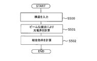
- FIG. 25 shows a flow of an optical electric field calculation method applied to a conventional waveguide analyzer.
- the conventional optical electric field calculation method first, structural data such as a refractive index distribution in the cross section of the waveguide and an electromagnetic field component is input (step S500).
- the optical electric field is calculated by the beam propagation method (step S501).
- the coupling efficiency of the waveguide is calculated based on the calculated optical electric field (step S502).
- the present invention has been made to solve the above-mentioned problems, and analyzes an optical connection structure even when the optical connection structure has an electromagnetic field distribution in which a large number of modes are combined.
- the purpose is to provide an analysis technology that can perform.
- the analysis device is distributed to the optical connection structure based on a setting unit that sets information about the structure of the optical connection structure and information about the structure of the optical connection structure. From the distribution of the electromagnetic field obtained by solving a partial differential equation with the electromagnetic field as an unknown to obtain the distribution of the electromagnetic field and the distribution of the electromagnetic field obtained by the solution solving unit, within a plane at a predetermined position of the optical connection structure. Based on the mode distribution and the time response of the electromagnetic field extracted by the data extraction unit and the data extraction unit that extracts the time response of the electromagnetic field at a predetermined position of the optical connection structure, And a characteristic analysis unit that analyzes optical characteristics related to the optical connection structure.
- the optical connection structure includes a first waveguide and a second waveguide, and an optical element that optically connects the first waveguide and the second waveguide to each other.
- the solution finding unit calculates a waveguide mode indicating an electromagnetic field in which eigenmodes of 0th order and higher are combined.
- a second distribution calculator that calculates a distribution of a reference electric field indicating a distribution of an electromagnetic field in a region included in the first waveguide and the optical element when an electromagnetic wave propagates.
- the solution finding unit includes an eigenmode calculating unit that calculates an eigenmode of the second waveguide, and the data extracting unit intersects with an optical axis of the second waveguide. And a mode distribution extraction unit that extracts a mode distribution in an arbitrary cross section, wherein the characteristic analysis unit includes the eigenmode calculated by the eigenmode calculation unit and the mode extracted by the mode distribution extraction unit.
- a coupling efficiency calculation unit that calculates a coupling efficiency between the eigenmode and the mode distribution based on the distribution may be included.
- the data extraction unit may have a first reference coordinate set at a position intersecting the optical axis of the optical element from the distribution of the electromagnetic field calculated by the first distribution calculation unit.
- a second response that is set at a position intersecting the optical axis of the second waveguide from the first response calculation unit that obtains the time change of the electric field in the second waveguide and the distribution of the electromagnetic field calculated by the first distribution calculation unit.
- a second response calculation unit that obtains a time change of the electric field at coordinates, and a third response calculation that obtains a time change of the reference electric field at the first reference coordinate from the distribution of the reference electric field calculated by the second distribution calculation unit. It may have a part.
- the characteristic analysis unit may change the electric field with time in the first reference coordinates obtained by the first response calculation unit and the reference electric field obtained by the third response calculation unit. It is also possible to have a reflectance calculation unit that calculates the reflectance at the first reference coordinates based on the change with time.
- the characteristic analysis unit may change the electric field at the second reference coordinates with time obtained by the second response calculation unit and the reference electric field obtained by the third response calculation unit. It is also possible to have a transmittance calculation unit that calculates the transmittance at the second reference coordinates based on the change with time.
- the optical connection structure set by the setting unit is set based on optical characteristics set in advance from the optical characteristics of the optical connection structure analyzed by the characteristic analysis unit.
- An evaluation unit for evaluating the structure may be further provided.
- the analysis method provides the optical connection structure based on the first step of setting information about the structure of the optical connection structure and the information about the structure of the optical connection structure. From the second step of solving a partial differential equation with the distributed electromagnetic field as an unknown to obtain the distribution of the electromagnetic field, and from the distribution of the electromagnetic field solved in the second step, a predetermined position of the optical connection structure In the in-plane mode distribution and a third step of obtaining the time response of the electromagnetic field at a predetermined position of the optical connection structure, and the mode distribution and the time response of the electromagnetic field obtained in the third step. And a fourth step of analyzing optical characteristics of the optical connection structure.
- a partial differential equation with an electromagnetic field distributed in an optical connection structure as an unknown is solved, and from the distribution of the solved electromagnetic waves, the in-plane mode distribution and electromagnetic field time at a predetermined position of the optical connection structure are solved. Since the response is extracted, the optical connection structure can be analyzed even when a large number of electromagnetic field modes are combined.
- FIG. 1 is a block diagram showing the structure of an analyzing apparatus according to an embodiment of the present invention.
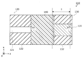
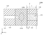
- FIG. 2 is a schematic plan view of the optical connection structure according to the present embodiment.
- FIG. 3 is a structural schematic diagram for calculating the reference electric field distribution according to the present embodiment.
- FIG. 4 is a block diagram showing the hardware configuration of the analysis device according to the present embodiment.
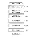
- FIG. 5 is a flowchart illustrating the method of analyzing the optical connection structure according to this embodiment.
- FIG. 6 is a flowchart illustrating the calculation processing of the eigenmode.
- FIG. 7 is a flowchart illustrating the calculation process of the guided mode.
- FIG. 8 is a flowchart illustrating the calculation processing of the electromagnetic field distribution.
- FIG. 1 is a block diagram showing the structure of an analyzing apparatus according to an embodiment of the present invention.
- FIG. 2 is a schematic plan view of the optical connection structure according to the present embodiment.
- FIG. 3 is a structural schematic diagram for calculating the reference
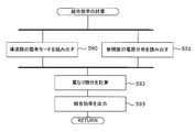
- FIG. 9 is a flowchart illustrating the calculation process of the coupling efficiency.
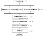
- FIG. 10 is a flowchart illustrating the reflectance calculation process.
- FIG. 11 is a flowchart illustrating the transmittance calculation processing.
- FIG. 12A is a diagram showing the structure of the first waveguide.
- FIG. 12B is a diagram showing an example of the electric field distribution of the first waveguide.
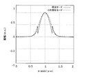
- FIG. 13 is a diagram showing an example of the waveguide mode of the first waveguide.
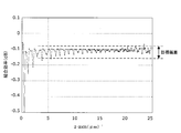
- FIG. 14 is a diagram illustrating the dependence of the coupling efficiency of the first waveguide on the position of the reference surface.
- FIG. 15 is a schematic plan view of an optical connection structure according to a specific example of the present embodiment.
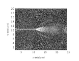
- FIG. 16A is a structural schematic diagram for calculating the reference electric field distribution according to the specific example.
- FIG. 16B is a diagram showing a reference electric field distribution according to the specific example.
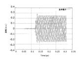
- FIG. 17 is a diagram showing the transient response of the reference electric field.
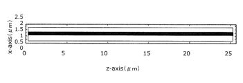
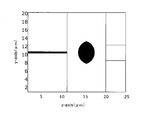
- FIG. 18A is a diagram showing an optical connection structure.
- FIG. 18B is a diagram showing an electric field distribution of the optical connection structure.
- FIG. 19 is a diagram showing the transient response of the electric field at the first reference coordinates.
- FIG. 20 is a diagram showing the transient response of the reflected electric field at the first reference coordinates.
- FIG. 21 is a diagram showing the transient response of the electric field at the second reference coordinates.
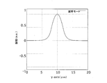
- FIG. 22 is a diagram showing eigenmodes of the second waveguide.
- FIG. 23 is a diagram showing the mode distribution of the second waveguide.
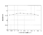
- FIG. 24 is a diagram for explaining the dependence of the coupling efficiency of the second waveguide on the reference plane position.
- FIG. 25 is a flowchart for explaining a conventional technique for analyzing an optical connection structure.
- the analysis device 1 analyzes the characteristics of the optical connection structure including minute optical elements.
- the analysis apparatus 1 analyzes the electromagnetic field distribution in the optical connection region that couples the waveguides having different mode fields, and determines the shape of the optical element that connects the two waveguides included in the optical connection structure. And determine the physical properties.
- the optical connection structure 110 to be analyzed by the analyzer 1 will be described with reference to FIG.
- the optical connection structure 110 includes a first waveguide 120, a second waveguide, and an optical element 140 that connects the first waveguide 120 and the second waveguide 130.
- the optical connection structure 110 converts the mode field of the light (electromagnetic wave) input to the first waveguide 120 and couples it to the second waveguide 130.
- the x, y, and z axes shown in each drawing including FIG. 2 are orthogonal to each other, and the vertical direction is the y axis, the horizontal direction is the x axis, and the light propagation direction, that is, the direction along the optical axis is the z axis. To do.
- a case will be described in which light is input from the first waveguide 120 and propagated to the second waveguide 130.
- the first waveguide 120 includes a core 121 and a clad 122 that covers the core 121.
- One end of the core 121 faces the core 131 of the second waveguide 130 via the optical element 140.
- the core 121 has, for example, a constant cross-sectional shape in the x-axis direction along the light propagation direction (z-axis).
- the end portion of the core 121 is formed in a rectangular parallelepiped shape.
- the cross-sectional area of the core 121 in the direction perpendicular to the light propagation direction (z axis) is larger than the cross-sectional area of the core 131 of the second waveguide 130 described later in the direction perpendicular to the light propagation direction (z axis). small.
- the clad 122 is formed so as to cover the core 121.
- the clad 122 is formed of, for example, a silicon oxide material.
- the core 121 is made of, for example, a Si material.
- the second waveguide 130 includes a core 131 and a clad 132 that covers the core 131.
- the second waveguide 130 constitutes, for example, an optical fiber.
- the core 131 is provided at the center of the second waveguide 130 and propagates the light whose mode field is converted by the first waveguide 120.
- the core 131 has, for example, a circular cross section.
- the clad 132 is formed so as to cover the outer peripheral surface of the core 131.
- the optical element 140 optically connects the first waveguide 120 and the second waveguide 130.
- the optical element 140 is arranged in a gap between the end surface of the first waveguide 120 and the end surface of the second waveguide 130 which faces the end surface.
- the analysis device 1 analyzes the optical connection structure 110 to determine whether or not the shape and physical property values of the optical element 140 need to be corrected.
- the analysis device 1 includes a setting unit 10, a solution finding unit 20, a data extraction unit 30, a characteristic analysis unit 40, an evaluation unit 50, and a data storage unit 60.
- the setting unit 10 includes a first structure setting unit 11, a second structure setting unit 12, and a third structure setting unit 13.
- the setting unit 10 is, for example, the optical connection structure 110 such as the distribution of the shapes and physical property values of the first waveguide 120, the second waveguide 130, and the optical element 140 according to an input signal input from the outside to the input device 107. Set the information about the structure of. Further, the setting unit 10 sets a mesh interval which is a divided region of the optical connection structure 110 used when the solution finding unit 20 calculates the characteristics of the optical connection structure 110.
- the first structure setting unit 11 sets the size of the shape of the first waveguide 120 and the distribution of the physical property values.
- the second structure setting unit 12 sets the size of the shape of the second waveguide 130 and the distribution of the physical property values.
- the third structure setting unit 13 sets the size of the shape of the optical element 140 and the distribution of the physical property values.
- the parameters indicating the set shape and physical property value of the optical connection structure 110 are stored in the data storage unit 60.
- the solution solver 20 includes an eigenmode calculator 21, a guided mode calculator 22, a first distribution calculator 23, and a second distribution calculator 24.
- the solution finding unit 20 finds the distribution of the electromagnetic field by solving a partial differential equation with the electromagnetic field distributed in the optical connection structure 110 as an unknown. Specifically, the solution finding unit 20 determines the waveguide mode of the first waveguide 120, the eigenmode of the second waveguide 130, and the distribution of the electromagnetic field propagating from the first waveguide 120 toward the second waveguide 130. Is solved based on the governing formula described later. Further, the solution finding unit 20 separates the traveling wave and the reflected wave from the electromagnetic field distribution by assuming that there is no electromagnetic field propagating toward the first waveguide 120 (“reference electric field”). "Distribution").
- the eigenmode calculation unit 21 calculates the eigenmode of the second waveguide 130 based on the shape of the second waveguide 130 and the distribution of the physical property values set by the second structure setting unit 12. More specifically, the eigenmode calculator 21 calculates the eigenmode using the finite element method.
- the eigenmode is a function representing the state of the system, and determines the energy distribution of the electromagnetic field localized in the core 131 of the second waveguide 130 in this system.
- the eigenmode calculation unit 21 uses the Helmholtz equation as a governing expression that determines the energy distribution of the electromagnetic field localized in the core 131, and obtains a function that represents the state of the system under certain boundary conditions, that is, an eigenmode. ..
- the eigenmode calculation unit 21 solves the Helmholtz equation of the above equation (1) by the finite element method.
- the coefficient of the term including the propagation constant ⁇ is called the separation coefficient.
- the eigenmode calculator 21 sets a separation coefficient determined by the refractive index distribution and the propagation constant of the second waveguide 130 and the wave number of propagating light. Further, the eigenmode calculation unit 21 sets a discretized finite element formula and sets boundary conditions. Specifically, the eigenmode calculation unit 21 assembles the finite element formula into a simultaneous equation based on the number of discretized state functions, and performs a matrix operation to obtain the state function. The eigenmode of the second waveguide 130 obtained by the eigenmode calculator 21 is used for the calculation of the coupling efficiency by the characteristic analyzer 40 described later.
- the waveguide mode calculation unit 22 calculates the waveguide mode of the first waveguide 120 using the shape of the first waveguide 120 and the distribution of physical property values set by the first structure setting unit 11.
- the guided mode of the first waveguide 120 means an electromagnetic field in which eigenmodes of 0th order and higher are combined when end face reflection does not occur.
- the first distribution calculation unit 23 and the second distribution calculation unit 24 calculate the electromagnetic field distribution in the boundary region of the optical connection structure 110.
- the first distribution calculator 23 calculates the electric field distribution of the optical connection structure 110.
- the second distribution calculator 24 calculates a reference electric field distribution, which is an electric field distribution in which the electromagnetic field propagating toward the first waveguide 120 does not exist even though it includes the optical element 140. That is, the reference electric field distribution is an electric field distribution when the optical element 140 does not include a structure that blocks a traveling wave propagating from the first waveguide 120 toward the second waveguide 130 side.
- the second distribution calculation unit 24 calculates the reference electric field distribution of the optical connection structure 110a composed of the first waveguide 120 and the optical element 140 shown in FIG.
- the optical element 140 included in the optical connection structure 110a is a uniform medium and has a structure that does not cause a change in wave number.
- the data extraction unit 30 extracts data including the mode distribution in the plane at a predetermined position of the optical connection structure 110 and the time response of the electromagnetic field from the electromagnetic field distribution solved by the solution finding unit 20.
- the data extraction unit 30 includes a mode distribution extraction unit 31, a first response calculation unit 32, a second response calculation unit 33, and a third response calculation unit 34.
- the mode distribution extraction unit 31 extracts the mode distribution of the designated reference section I of the optical connection structure 110 shown in FIG. 2 based on the electric field distribution of the optical connection structure 110 calculated by the first distribution calculation unit 23. ..
- As the reference section I an arbitrary cross section that intersects the optical axis in the second waveguide 130 may be used.
- the first response calculation unit 32 obtains the transient response of the electric field at the first reference coordinates p1 of the optical connection structure 110 shown in FIG.
- the first reference coordinate p1 is set within the area of the optical connection structure 110 including the optical element 140.
- the first reference coordinate p1 is set at the position of the optical element 140 where the optical axis intersects the optical element 140.
- the second response calculation unit 33 obtains the transient response of the electric field at the second reference coordinates p2 of the optical connection structure 110 shown in FIG.
- the second reference coordinate p2 is set within the area of the second waveguide 130.
- the second reference coordinate p2 is set at a position intersecting the optical axis in the second waveguide 130.
- the third response calculation unit 34 obtains a transient response of the reference electric field at the first reference coordinate p1 based on the reference electric field distribution calculated by the second distribution calculation unit 24.
- the characteristic analysis unit 40 analyzes the optical characteristics of the optical element 140 based on the mode distribution and the time response of the electromagnetic field extracted by the data extraction unit 30. Specifically, the characteristic analysis unit 40, based on the electric field distribution extracted by the data extraction unit 30 and the eigenmode of the second waveguide 130 calculated by the eigenmode calculation unit 21, performs coupling in an arbitrary reference section I. Calculate efficiency, reflectance and transmittance at arbitrary reference coordinates.
- the characteristic analysis unit 40 includes a coupling efficiency calculation unit 41, a reflectance calculation unit 42, and a transmittance calculation unit 43.
- the coupling efficiency calculation unit 41 calculates the coupling efficiency CE between the eigenmode and the mode distribution of the second waveguide 130 in the arbitrary reference section I of the optical connection structure 110.
- the coupling efficiency CE indicates how much the electric field distribution E on an arbitrary reference surface of the optical connection structure 110 matches the eigenmode ⁇ m of the first waveguide 120 or the second waveguide 130, and is expressed by the following equation (2). It is obtained by calculating the overlap integral defined by.
- the optical axis of the waveguide is parallel to the z-axis direction, and the z coordinate of the point where the reference plane intersects the optical axis is Z ref .
- the reflectance calculation unit 42 calculates the transient response of the standard electric field obtained by the third response calculation unit 34 and the transient response of the electric field at the first reference coordinate p1 of the optical connection structure 110 obtained by the first response calculation unit 32. Based on and, the reflectance at the first reference coordinate p1 is calculated.
- the transmittance calculator 43 receives the transient response of the standard electric field obtained by the third response calculator 34 and the transient response of the electric field at the second reference coordinate p2 of the optical connection structure 110 obtained by the second response calculator 33.
- the transmittance is calculated based on and.
- the evaluation unit 50 evaluates the structure of the optical element 140 set by the setting unit 10 based on the optical characteristics set in advance from the optical characteristics of the optical element 140 analyzed by the characteristic analysis unit 40. More specifically, the evaluation unit 50 determines the shape of the optical element 140 included in the optical connection structure 110 from the optical characteristics including the coupling efficiency, reflectance, and transmittance of the optical connection structure 110 output by the characteristic analysis unit 40. It is determined whether or not the property value needs to be modified.
- the data storage unit 60 stores the structure data of the optical connection structure 110 set by the setting unit 10. In addition, the data storage unit 60 stores the eigenmode, guided mode, and electromagnetic field distribution calculated by the solution finding unit 20. The data storage unit 60 also stores the mode distribution, the transient response of the electric field, and the like extracted by the data extraction unit 30. The data storage unit 60 also stores the coupling efficiency, the reflectance, and the transmittance calculated by the characteristic analysis unit 40.
- the analysis device 1 includes, for example, a processor 102, a main storage device 103, a communication interface 104, an auxiliary storage device 105, an I/O device 106, and an input device 107 that are connected via a bus 101. It can be realized by a computer and a program that controls these hardware resources.
- the display device 108 is connected via the bus 101, and the analysis result and the calculation process by the analysis device 1 such as the structural data of the optical connection structure 110, the coupling efficiency, the reflectance, and the transmittance are displayed on the display screen. May be displayed.
- the main storage device 103 is realized by a semiconductor memory such as SRAM, DRAM, and ROM. Programs for the processor 102 to perform various controls and calculations are stored in the main storage device 103 in advance.
- the processor 102 and the main storage device 103 realize each function of the analysis device 1 including the setting unit 10, the solution finding unit 20, the data extracting unit 30, the characteristic analyzing unit 40, and the evaluating unit 50 illustrated in FIG. 1.
- the communication interface 104 is an interface circuit for communicating with various external electronic devices via the communication network NW.
- the analysis device 1 may send the analysis result to the outside via the communication interface 104.
- the communication interface 104 for example, an interface and an antenna compatible with wireless data communication standards such as LTE, 3G, wireless LAN, and Bluetooth (registered trademark) are used.
- the communication network NW includes, for example, a WAN (Wide Area Network), a LAN (Local Area Network), the Internet, a dedicated line, a wireless base station, a provider, and the like.
- the auxiliary storage device 105 is composed of a readable/writable storage medium and a drive device for reading/writing various information such as programs and data from/to the storage medium.
- a semiconductor memory such as a hard disk or a flash memory can be used as a storage medium.
- the auxiliary storage device 105 has a program storage area for storing a program for the analysis device 1 to perform the analysis processing of the optical connection structure 110. Further, the auxiliary storage device 105 may have, for example, a backup area for backing up the above-mentioned data and programs.
- the auxiliary storage device 105 stores, for example, a structure setting program 105a, a solution finding program 105b, a data extraction program 105c, a characteristic analysis program 105d, and an evaluation program 105e in the program storage area.
- the auxiliary storage device 105 also has a data storage area 105f.
- the data storage area 105f realizes the data storage unit 60 described in FIG.
- the I/O device 106 is configured by an I/O terminal that inputs a signal from an external device such as the display device 108 and outputs a signal to the external device.
- the input device 107 is composed of a keyboard, a touch panel, and the like, and generates an input signal according to a key press or touch operation.
- the setting unit 10 described in FIG. 1 sets the structural data of the optical connection structure 110 according to the input signal generated by the input device 107.
- the analysis device 1 is not limited to being realized by one computer, but may be distributed by a plurality of computers connected to each other by the communication network NW.
- the setting unit 10 sets the mesh interval of the optical connection structure 110 used in the calculation by the solution finding unit 20 (step S1).
- the setting unit 10 sets the shape of the optical connection structure 110 and the distribution of the physical property values (step S2). More specifically, the first structure setting unit 11 sets the shape of the first waveguide 120 and the distribution of physical property values.
- the second structure setting unit 12 sets the shape of the second waveguide 130 and the distribution of the physical property values.
- the third structure setting unit 13 sets the shape of the optical element 140 and the distribution of physical property values.
- the mesh spacing and the shape and distribution of physical property values of the optical connection structure 110 set in step S1 and step S2 are stored in the data storage unit 60.
- the eigenmode calculator 21 calculates the eigenmode of the second waveguide 130 (step S3).
- the calculation process of the eigenmode of the second waveguide 130 will be described with reference to FIG.
- the eigenmode calculation unit 21 calculates the separation coefficient of the above-described formula (1) determined by the refractive index distribution and the propagation constant of the second waveguide 130 and the wave number of the propagating light. Set (step S3).
- the eigenmode calculator 21 sets the discretized finite element formula based on the formula (1) (step S31).
- the eigenmode calculation unit 21 sets boundary conditions (step S32).
- the eigenmode calculation unit 21 assembles the set finite element equations into simultaneous equations based on the number of discretized state functions, and performs matrix calculation (step S33).
- the eigenmode calculation unit 21 obtains and outputs a state function by matrix calculation (step S34).
- the output state function is stored in the data storage unit 60.
- the eigenmode calculation unit 21 adds the step of the propagation constant ⁇ in the equation (1) (step S35).
- step S36 NO
- step S36 NO
- step S37 the eigenmode calculation unit 21 outputs the eigenmode (step S37).
- the eigenmode calculator 21 obtains a spectrum showing the relationship between the state function and the propagation constant, selects at least one predetermined peak from the spectrum, and selects those peaks as the eigenmode ⁇ m (m is Output as an integer of 0 or more).
- the eigenmode calculation unit 21 may subtract the value of the propagation constant instead of adding the value of the propagation constant in step S35, and repeat the processing from step S30 to step S34 until the lower limit value is reached. Thereafter, the processing shifts to step S9 in FIG.
- the guided mode calculator 22 calculates the guided mode of the first waveguide 120 after step S2 (step S4).
- the calculation processing of the guided mode will be described with reference to FIG. 7.
- the waveguide mode calculation unit 22 reads the shape of the first waveguide 120 and the distribution of the physical property values stored in the data storage unit 60 (step S40). Next, the guided mode calculator 22 calculates the eigenmode of the first waveguide 120 by the finite element method (step S41).
- the waveguide mode calculation unit 22 uses the above-described finite element method based on the structure of the first waveguide 120 shown in FIG. 12A to perform the eigenmode EIG1 of the first waveguide 120 shown by the broken line in FIG. To calculate.
- the guided mode calculator 22 calculates the eigenmode EIG1 by the same procedure as the eigenmode calculation process described in FIG. Note that FIG. 13 shows an example in which the 0th-order eigenmode is obtained.
- the waveguide mode calculation unit 22 calculates the electric field distribution EH1 of the first waveguide 120 by the time-domain difference (Finite-difference Time-domain: FDTD) method, which is an electromagnetic field analysis method (step S42).
- the FDTD method is a method for obtaining the electric field distribution in the time domain by differentiating Maxwell's equations in time and space.
- the waveguide mode calculation unit 22 applies the eigenmode EIG1 of the first waveguide 120 obtained by the finite element method to the light source, and obtains the electric field distribution EH1 shown in FIG. 12B by the FDTD method.
- the details of the calculation process of the electromagnetic field distribution by the FDTD method used in step S42 will be described later.
- the guided mode calculator 22 guides a predetermined specified section along the direction perpendicular to the optical axis of the first waveguide 120 from the electric field distribution EH1 of the first waveguide 120 calculated by the FDTD method.
- the mode distribution M k is obtained (step S43).
- k represents the identification number of the coordinate in the section where the guided mode distribution is extracted.
- the guided mode calculator 22 may obtain the guided mode distribution M k in a preset designated section along the plane perpendicular to the optical axis of the first waveguide 120.
- the solid line in FIG. 13 shows an example of the guided mode distribution M k of the first waveguide 120 extracted by the guided mode calculator 22.
- the guided mode calculator 22 calculates the guided mode distribution of the first waveguide 120 using the FDTD method, thereby calculating the mode reflecting the refractive index difference.
- the guided mode calculator 22 calculates the coupling efficiency between the eigenmode EIG1 of the first waveguide 120 and the guided mode M k in order to select a more stable guided mode solution (step S44).
- the waveguide mode calculation unit 22 obtains the relationship between the coupling efficiency and the position of the first waveguide 120 in the z-axis direction, as shown in FIG.
- the guided mode calculator 22 selects and outputs the guided mode M s corresponding to the coupling efficiency within the range of the preset target deviation (arrow in FIG. 14). The details of the calculation processing of the coupling efficiency by the waveguide mode calculation unit 22 will be described later.
- the guided mode calculator 22 outputs the guided mode of the first waveguide 120 (step S45). Thereafter, the processing shifts to step S5 and step S7 in FIG.
- the second distribution calculator 24 calculates the reference electric field distribution of the optical connection structure 110a when it is assumed that there is no electromagnetic field propagating toward the first waveguide 120 (Ste S5).
- the first distribution calculator 23 calculates the electric field distribution of the optical connection structure 110 (step S7).
- step S5 the calculation processing of the electromagnetic field distribution in step S5, step S7, and step S42 (FIG. 7) will be described with reference to FIG.
- the first distribution calculator 23 initializes the electric field and magnetic field of the optical connection structure 110 (step S70).
- the first distribution calculation unit 23 determines that the first waveguide The guided mode M s of 120 is read from the data storage unit 60 (step S71).
- the first distribution calculation unit 23 defines a light source (step S72). Specifically, the optical axis of the first waveguide 120 is parallel to the z-axis direction, and the electric field distribution at the coordinates where the light source polarized in the x-axis direction is set is defined by the following equation (3).
- Ex is an electric field vector component in the x-axis direction
- i and j are respectively discretized.
- the coordinate components in the x and y axis directions are shown.
- ks represents an arbitrary z-axis coordinate on the optical axis of the first waveguide 120.
- the second term on the right side of the above equation (3) is an excitation source that vibrates with a sine wave or a cosine wave with respect to time n ⁇ t, the coefficient ⁇ is the angular vibration frequency, and ⁇ t is the time interval.
- a light source of this type is called a soft source, while a light source consisting of only the excitation source is called a hard source.
- the Hard source does not allow the transmission of other waves at the coordinates of the light source itself and gives an inconvenient solution when compared with the actual phenomenon, so it is not normally used as the light source.
- Soft source is desirable as a normal light source because it allows the transmission of other waves and has no interference.
- the first distribution calculation unit 23 sets the dielectric constant and the magnetic permeability of the optical connection structure 110 so that the central axis of the light source defined in step S52 and the central axis of the core 121 of the first waveguide 120 match. , And the distribution of conductivity are set (step S73).
- the first distribution calculator 23 calculates the electric field distribution according to the Yee algorithm (step S74).
- the Yee algorithm the Maxwell equation is calculated by dividing the analysis region into a calculation grid called a Yee lattice in which an electric field and a magnetic field are shifted from each other by a half lattice.
- the first distribution calculation unit 23 applies the PML absorption boundary condition or the Mur absorption boundary condition to the outer circumference of the region, and calculates the electric field in the boundary region (step S75).
- the first distribution calculation unit 23 updates the electric field at the coordinates (i, j, ks) where the light source is set according to the above equation (3) (step S76).
- the following steps S77 and S78 may be executed. Specifically, the magnetic field distribution is also calculated according to the Yee algorithm similarly to the electric field (step S77). Next, the PML absorbing boundary condition or the Mur absorbing boundary condition is applied to the outer circumference of the region to calculate the magnetic field in the boundary region (step S78).
- the first distribution calculation unit 23 outputs the calculated electric field (step S79).
- the magnetic field is output in step S79.
- step S80 the second distribution calculation unit 24 adds time steps (step S80). After that, the processes of steps S74 to S79 are repeated until the upper limit of the time is reached (step S81: NO). If the time limit has been reached (step S81: YES), the process returns to the process of FIG.
- step S5 after the second distribution calculation unit 24 calculates the reference electric field distribution based on the above electromagnetic field distribution calculation processing (step S5), the third response calculation unit 34 sets the reference electric field distribution to the reference electric field distribution.
- the transient response of the reference electric field is extracted from the electric field distribution (step S6). Then, a process transfers to step S11.
- the mode distribution extractor 31 extracts the mode distribution of the reference section I shown in FIG. 2 (step S8).
- the coupling efficiency calculation unit 41 calculates the coupling efficiency of the optical connection structure 110 (step S9).
- FIG. 9 is a flow chart showing the calculation processing (step S9) of the coupling efficiency.
- the coupling efficiency is calculated in the same procedure in the guided mode calculation process (FIG. 7) (step S44 in FIG. 7).
- the coupling efficiency calculation unit 41 reads the eigenmode ⁇ m of the second waveguide 130 from the data storage unit 60 (step S90).
- the coupling efficiency calculation unit 41 reads out the electric field distribution of an arbitrary reference plane in the optical connection structure 110 from the data storage unit 60 (step S91).
- the electric field distribution in the optical connection structure 110 is the value calculated by the first distribution calculation unit 23 in step S7.
- the coupling efficiency calculation unit 41 calculates the overlap integral defined by the above equation (2) (step S92). Then, the coupling efficiency calculation unit 41 outputs the calculated coupling efficiency (step S93). After that, the process proceeds to step S13 of FIG.
- step S10 the transient response of the electric field at the first reference coordinate p1 and the second reference coordinate p2 is obtained (step S10).
- the reflectance calculator 42 calculates the reflectance based on the transient response of the standard electric field calculated in step S6 and the transient response of the electric field at the first reference coordinate p1 (step S11).
- the transmittance calculator 43 calculates the transmittance of the optical connection structure 110 based on the transient response of the electric field at the second reference coordinate p2 (step S12).
- the reflectance calculator 42 reads the transient response of the reference electric field from the data storage 60 (step S110). Further, the reflectance calculation unit 42 reads the transient response of the electric field at the first reference coordinate p1 from the data storage unit 60 (step S111).
- the reflectance calculator 42 calculates the reference electric field F inc ( ⁇ ) in the frequency domain (step S113). Specifically, the reflectance calculation unit 42 performs a Fourier transform on the transient response E inc (t) of the reference electric field in a predetermined time section (t ref 1 ⁇ t ⁇ t ref 2) to obtain the frequency. The reference electric field F inc ( ⁇ ) of the region is obtained.
- the transmittance calculator 43 reads the reference electric field F inc ( ⁇ ) in the frequency domain (step S113 in FIG. 10) calculated in the reflectance calculation process from the data storage 60 (step S120). Further, the transmittance calculator 43 reads out the transient response E2 tot (t) of the electric field at the second reference coordinate p2 from the data storage 60 (step S121).
- the transmittance calculator 43 calculates the transmission electric field F trn ( ⁇ ) in the frequency domain (step S122). Specifically, the transmittance calculator 43 calculates the time change E trn (t) of the transmission electric field with respect to the transient response E2 tot (t) of the electric field at the second reference coordinate p2 in a predetermined time section (t trn 1 ⁇ At t ⁇ t trn 2), a Fourier transform is performed to obtain a transmission electric field F trn ( ⁇ ) in the frequency domain.
- the evaluation unit 50 determines that it is necessary to correct the shape and the physical property value of the optical element 140 of the optical connection structure 110 based on the preset requirement regarding the characteristics of the optical element 140. In that case (step S13: NO), the processes of steps S2 to S12 are repeated. On the other hand, when the evaluation unit 50 determines that the shape or the physical property value of the optical element 140 does not need to be corrected (step S13: YES), the process ends.
- the evaluation unit 50 determines, based on the coupling efficiency calculated in step S9, the reflectance calculated in step S11, and the transmittance calculated in step S12, the desired coupling efficiency and reflection of the optical connection structure 110. It is determined whether or not the shape and physical property values of the optical element 140 need to be corrected depending on whether the refractive index and the transmittance are satisfied.
- the analysis device 1 analyzes the optical connection structure 110.
- the optical connection structure 110b which is the target of analysis by the analysis device 1, will be described.
- the optical connection structure 110b has a first waveguide 120 and a second waveguide 130, and an adhesive layer 140b which is an optical element connecting these waveguides.
- the first waveguide 120 is formed of, for example, a buried Si waveguide.
- the first waveguide 120 has a core 121 and a clad 122 formed so as to cover the core 121.
- an optical fiber made of a silica-based material is used for the second waveguide 130.
- the second waveguide 130 has a core 131 of an optical fiber and a clad 132 formed so as to cover the core 131.
- the adhesive layer 140b is formed, for example, so that the end faces of the first waveguide 120 and the second waveguide 130 facing each other are filled with an adhesive formed of a resin material such as an epoxy resin or an acrylic resin.
- the adhesive layer 140b has a lens 141b formed on the optical axes of the first waveguide 120 and the second waveguide 130.
- the lens 141b is formed of a spherical lens that is convex along the optical axis.
- the lens 141b is made of a resin material. Note that the adhesive layer 140b is formed so that its refractive index is smaller than that of the lens 141b.
- the region of the optical connection structure 110b is assumed to be a slab waveguide in which the refractive index does not change in the x-axis direction.
- the first reference coordinate p1 is set on the optical axis in the area of the adhesive layer 140b.
- the second reference coordinate p2 is set on the optical axis in the region of the second waveguide 130.
- FIG. 16A shows a region structure for calculating the distribution of the reference electric field of the optical connection structure 110b.
- 16B shows the reference electric field distribution of the optical connection structure 110b calculated by the second distribution calculation unit 24. Note that FIG. 16B shows the square distribution of the electric field.
- the reference electric field is calculated in the structure of only the first waveguide 120 and the adhesive layer 140b that does not include the lens 141b. That is, the electric field distribution when the adhesive layer 140b, which is an optical element, does not include a structure that blocks a traveling wave propagating from the first waveguide 120 toward the second waveguide 130 side is calculated as the reference electric field distribution. ..
- FIG. 17 shows the transient response of the reference electric field at the first reference coordinate p1 set in the adhesive layer 140b of the optical connection structure 110b, which is obtained by the third response calculation unit 34.
- the horizontal axis represents time and the vertical axis represents amplitude.
- FIG. 18A shows a region structure of the optical connection structure 110b.
- FIG. 18B shows the electric field distribution of the optical connection structure 110b of FIG. 18A calculated by the first distribution calculator 23. Note that FIG. 18B shows the square distribution of the electric field.
- FIG. 19 shows the transient response of the electric field at the first reference coordinate p1 of the optical connection structure 110b, which is obtained by the first response calculation unit 32 based on the electric field distribution output by the first distribution calculation unit 23.
- the horizontal axis of FIG. 19 represents time and the vertical axis represents amplitude.
- FIG. 20 shows the time change of the reflected electric field calculated by the reflectance calculation unit 42 based on the transient response of the electric field at the first reference coordinate p1.
- the horizontal axis of FIG. 20 represents time and the vertical axis represents amplitude.
- FIG. 21 shows the transient response of the electric field at the second reference coordinate p2 obtained by the second response calculation unit 33 from the electric field distribution of the optical connection structure 110b.
- the horizontal axis represents time and the vertical axis represents amplitude.
- FIG. 22 shows the eigenmode (0th order) of the second waveguide 130 calculated by the eigenmode calculator 21.
- FIG. 23 shows a result of the mode distribution extraction unit 31 calculating the mode distribution on the reference plane a defined in the reference section I of the second waveguide 130 shown in FIG.
- the mode distribution shown in FIG. 23 shows a representative value of the mode distribution in the y-axis direction.
- FIG. 24 the coupling efficiency calculated by the coupling efficiency calculation unit 41 based on the mode distribution by displacing the position of the reference plane a set in the second waveguide 130 and the distance of the second waveguide 130.
- the result of having plotted the relationship of is shown.
- the horizontal axis of FIG. 24 indicates the distance D (FIG. 14) from the right end of the reference section I along the z-axis.
- the vertical axis represents the coupling efficiency [dB].
- the waveguide mode of the waveguide in which the eigenmodes of 0th order and higher are combined is calculated, and the calculated waveguide mode is used as the light source in the FDTD method. Since the electromagnetic field distribution of the optical connection structure is calculated by, it is possible to analyze the optical connection structure even when a large number of electromagnetic field modes are combined.
- Lens 121, 131... Core, 122, 132... Clad, 101... Bus, 102... Processor, 103... Main Storage device 104... Communication interface 105... Auxiliary storage device 106... I/O device 107... Input device 108... Display device.
Landscapes
- Physics & Mathematics (AREA)
- General Physics & Mathematics (AREA)
- Engineering & Computer Science (AREA)
- Mathematical Physics (AREA)
- Chemical & Material Sciences (AREA)
- Computational Mathematics (AREA)
- Mathematical Analysis (AREA)
- Mathematical Optimization (AREA)
- Pure & Applied Mathematics (AREA)
- Analytical Chemistry (AREA)
- Theoretical Computer Science (AREA)
- Data Mining & Analysis (AREA)
- Optics & Photonics (AREA)
- Geometry (AREA)
- Databases & Information Systems (AREA)
- Software Systems (AREA)
- General Engineering & Computer Science (AREA)
- Algebra (AREA)
- Life Sciences & Earth Sciences (AREA)
- Electrochemistry (AREA)
- Health & Medical Sciences (AREA)
- Chemical Kinetics & Catalysis (AREA)
- Operations Research (AREA)
- Biochemistry (AREA)
- General Health & Medical Sciences (AREA)
- Immunology (AREA)
- Pathology (AREA)
- Microelectronics & Electronic Packaging (AREA)
- Computing Systems (AREA)
- Optical Integrated Circuits (AREA)
- Testing Of Optical Devices Or Fibers (AREA)
Abstract
光接続構造が、多数のモードが複合された電磁界の分布となっている場合であっても、光接続構造を解析することができる解析技術を提供することを目的とする。 解析装置1は、光接続構造110の構造に関する情報を設定する設定部10と、光接続構造110に関する情報に基づいて、光接続構造110に分布する電磁界を未知数とした偏微分方程式を求解して電磁界の分布を求める求解部20と、求解部20が求解した電磁界の分布から、光接続構造110の所定の位置における面内でのモード分布、および光接続構造110の所定の位置での電磁界の時間応答を抽出するデータ抽出部30と、データ抽出部30が抽出したモード分布および電磁界の時間応答に基づいて、光接続構造110に関する光学的な特性を解析する特性解析部40とを備える。
Description
本発明は、解析装置および解析方法に関し、特に、光接続構造を解析する技術に関する。
近年、通信の大容量化に伴い光通信機器の小型化および高密度化が要求されている。光通信機器の構成要素である導波路間の光接続構造を解析する技術は一層重要となっている。従来から、領域サイズが比較的大きい光接続構造の結合特性を解析する場合には、光線追跡法がよく用いられている。また、導波路単体に対してであれば、ビーム伝搬法のような波動光学をベースにした結合特性の解析方法が採られる。
例えば、特許文献1では、ビーム伝搬法を用いて導波路を伝搬する光電界を近似して、光透過特性を模擬する導波路の解析装置を開示している。また、図25は、従来の導波路の解析装置に適用される光電界計算方法のフローを示している。従来の光電界計算方法では、まず、導波路の断面の屈折率分布、電磁界成分などの構造データが入力される(ステップS500)。次に、ビーム伝搬法により、光電界が計算される(ステップS501)。その後、計算した光電界に基づいて、導波路の結合効率が計算される(ステップS502)。
例えば、Si導波路と光ファイバなど、2つ以上の高い屈折率差を有する導波路間を結合する場合、テーパ、グレーディング、微小レンズ等、多様な光接続構造が介在する。このような光接続構造における接続間の微小領域では、多数のモードが複合された電磁界の分布となっている。そのため、従来のビーム伝搬近似を用いた解析技術では、光接続構造の透過特性の予測など、光接続構造の解析が困難であった。
本発明は、上述した課題を解決するためになされたものであり、光接続構造が、多数のモードが複合された電磁界の分布となっている場合であっても、光接続構造を解析することができる解析技術を提供することを目的とする。
上述した課題を解決するために、本発明に係る解析装置は、光接続構造の構造に関する情報を設定する設定部と、前記光接続構造の前記構造に関する情報に基づいて、前記光接続構造に分布する電磁界を未知数とした偏微分方程式を求解して前記電磁界の分布を求める求解部と、前記求解部が求解した前記電磁界の分布から、前記光接続構造の所定の位置における面内でのモード分布、および前記光接続構造の所定の位置での電磁界の時間応答を抽出するデータ抽出部と、前記データ抽出部が抽出した前記モード分布および前記電磁界の時間応答に基づいて、前記光接続構造に関する光学的な特性を解析する特性解析部とを備える。
また、本発明に係る解析装置において、前記光接続構造は、第1導波路および第2導波路と、前記第1導波路と前記第2導波路とを互いに光学的に接続する光学素子とを含み、前記求解部は、前記第1導波路に対し、前記光学素子側の端面での反射が発生しない場合において、0次以上の固有モードが複合した電磁界を示す導波モードを計算する導波モード計算部と、前記導波モードに基づいて、前記光接続構造に含まれる領域の電磁界の分布を計算する第1分布計算部と、前記第1導波路から前記第2導波路に向かって電磁波が伝搬したときの前記第1導波路および前記光学素子に含まれる領域の電磁界の分布を示す基準電界の分布を計算する第2分布計算部とを有していてもよい。
また、本発明に係る解析装置において、前記求解部は、前記第2導波路の固有モードを計算する固有モード計算部を有し、前記データ抽出部は、前記第2導波路の光軸と交差する任意の断面内におけるモード分布を抽出するモード分布抽出部を有し、前記特性解析部は、前記固有モード計算部によって計算された前記固有モードと、前記モード分布抽出部によって抽出された前記モード分布とに基づいて、前記固有モードと前記モード分布との結合効率を計算する結合効率計算部を有していてもよい。
また、本発明に係る解析装置において、前記データ抽出部は、前記第1分布計算部が計算した前記電磁界の分布から、前記光学素子の光軸と交差する位置に設定された第1参照座標での電界の時間変化を求める第1応答計算部と、前記第1分布計算部が計算した前記電磁界の分布から、前記第2導波路の光軸と交差する位置に設定された第2参照座標での電界の時間変化を求める第2応答計算部と、前記第2分布計算部が計算した前記基準電界の分布から、前記第1参照座標での基準電界の時間変化を求める第3応答計算部とを有していてもよい。
また、本発明に係る解析装置において、前記特性解析部は、前記第1応答計算部が求めた前記第1参照座標での電界の時間変化と、前記第3応答計算部が求めた前記基準電界の時間変化とに基づいて、前記第1参照座標での反射率を計算する反射率計算部を有していてもよい。
また、本発明に係る解析装置において、前記特性解析部は、前記第2応答計算部が求めた前記第2参照座標での電界の時間変化と、前記第3応答計算部が求めた前記基準電界の時間変化とに基づいて、前記第2参照座標での透過率を計算する透過率計算部を有していてもよい。
また、本発明に係る解析装置において、前記特性解析部が解析した前記光接続構造に関する光学的な特性から、予め設定された光学的な特性に基づいて、前記設定部が設定した前記光接続構造の構造を評価する評価部をさらに備えていてもよい。
上述した課題を解決するために、本発明に係る解析方法は、光接続構造の構造に関する情報を設定する第1ステップと、前記光接続構造の前記構造に関する情報に基づいて、前記光接続構造に分布する電磁界を未知数とした偏微分方程式を求解して前記電磁界の分布を求める第2ステップと、前記第2ステップで求解された前記電磁界の分布から、前記光接続構造の所定の位置における面内でのモード分布、および前記光接続構造の所定の位置での電磁界の時間応答を求める第3ステップと、前記第3ステップで求められた前記モード分布および前記電磁界の時間応答に基づいて、前記光接続構造に関する光学的な特性を解析する第4ステップとを備える。
本発明によれば、光接続構造に分布する電磁界を未知数とした偏微分方程式を求解し、求解した電磁波の分布から、光接続構造の所定の位置における面内のモード分布と電磁界の時間応答を抽出するので、多数の電磁界のモードが複合されている場合であっても、光接続構造を解析することができる。
以下、本発明の好適な実施の形態について、図1から図24を参照して詳細に説明する。
本実施の形態に係る解析装置1は、微小な光学素子を含む光接続構造の特性を解析する。特に、本実施の形態に係る解析装置1は、モードフィールドが異なる導波路を結合する光接続領域における電磁界分布を解析し、光接続構造に含まれる2つの導波路を接続する光学素子の形状や物性値を決定する。
まず、解析装置1が解析を行う対象である光接続構造110について図2を参照して説明する。図2の平面模式図に示すように、光接続構造110は、第1導波路120、第2導波路、および第1導波路120と第2導波路130とを接続する光学素子140を備える。
光接続構造110は、第1導波路120に入力される光(電磁波)のモードフィールドを変換して第2導波路130に結合させる。以下において、図2を含む各図に示すx、y、z軸は互いに直交し、鉛直方向をy軸、水平方向をx軸、光の伝搬方向、すなわち光軸に沿った方向をz軸とする。また、本実施の形態では、第1導波路120から光が入力されて第2導波路130に伝搬される場合について説明する。
第1導波路120は、コア121と、コア121を覆うクラッド122とを備える。コア121の一端は、光学素子140を介して第2導波路130のコア131と対向している。コア121は、例えば、光の伝搬方向(z軸)に沿って、x軸方向の断面形状が一定に維持される。例えば、コア121の端部は、直方体形状に形成される。なお、コア121の光の伝搬方向(z軸)に垂直な方向の断面積は、後述する第2導波路130が有するコア131の光伝搬方向(z軸)に垂直な方向の断面積よりも小さい。
クラッド122は、コア121を覆うように形成されている。クラッド122は、例えば、酸化シリコン材料から形成される。また、コア121は、例えば、Si材料によって形成される。
第2導波路130は、コア131と、コア131を覆うクラッド132とを備える。第2導波路130は、例えば、光ファイバを構成する。コア131は、第2導波路130の中心部に設けられ、第1導波路120によってモードフィールドが変換された光を伝搬する。コア131は、例えば、円形断面を有する。クラッド132は、コア131の外周面を覆うように形成されている。
光学素子140は、第1導波路120と第2導波路130とを光学的に接続する。光学素子140は、第1導波路120の端面と対向する第2導波路130の端面との間隙に配設される。本実施の形態では、解析装置1によって光接続構造110の解析を行い、光学素子140の形状や物性値の修正が必要であるか否かを判断する。
[解析装置の機能ブロック]
次に、本実施の形態に係る光接続構造110の解析装置1の機能構成について、図1を参照して説明する。
図1に示すように、解析装置1は、設定部10、求解部20、データ抽出部30、特性解析部40、評価部50、およびデータ格納部60を備える。
次に、本実施の形態に係る光接続構造110の解析装置1の機能構成について、図1を参照して説明する。
図1に示すように、解析装置1は、設定部10、求解部20、データ抽出部30、特性解析部40、評価部50、およびデータ格納部60を備える。
設定部10は、第1構造設定部11、第2構造設定部12、および第3構造設定部13を備える。設定部10は、例えば、外部から入力装置107へ入力される入力信号に応じて、第1導波路120、第2導波路130、および光学素子140の形状および物性値の分布など光接続構造110の構造に関する情報を設定する。また、設定部10は、求解部20が光接続構造110の特性を計算する際に用いる光接続構造110の分割領域であるメッシュ間隔を設定する。
第1構造設定部11は、第1導波路120の形状の寸法および物性値の分布を設定する。第2構造設定部12は、第2導波路130の形状の寸法および物性値の分布を設定する。第3構造設定部13は、光学素子140の形状の寸法および物性値の分布を設定する。設定された光接続構造110の形状および物性値を示すパラメータは、データ格納部60に記憶される。
求解部20は、固有モード計算部21、導波モード計算部22、第1分布計算部23、および第2分布計算部24を備える。求解部20は、光接続構造110に分布する電磁界を未知数とした偏微分方程式を求解して電磁界の分布を求める。具体的には、求解部20は、第1導波路120の導波モードと第2導波路130の固有モード、および第1導波路120から第2導波路130に向かって伝搬する電磁界の分布を、後述する支配式に基づいて求解する。また、求解部20は、電磁界分布から、進行波と反射波とを分離するために、第1導波路120に向かって伝搬する電磁界が存在しないと仮定した場合の電界分布(「基準電界分布」という。)を求解する。
固有モード計算部21は、第2構造設定部12によって設定された第2導波路130の形状、物性値の分布に基づいて、第2導波路130の固有モードを計算する。より詳細には、固有モード計算部21は、有限要素法を用いて固有モードを計算する。固有モードは、系の状態を表す関数であり、この系において、第2導波路130のコア131内に局在する電磁界のエネルギー分布を決める。
固有モード計算部21は、コア131内に局在する電磁界のエネルギー分布を決める支配式として、ヘルムホルツ方程式を用いて、一定の境界条件の下で系の状態を表す関数、すなわち固有モードを求める。伝搬定数β、屈折率n、波数ka(ka=2π/λ)、非斉次項fに依存して定義された状態関数φを未知数とするヘルムホルツ方程式は次式(1)で表される。

固有モード計算部21は、上式(1)のヘルムホルツ方程式を有限要素法によって求解する。なお、上式(1)において、伝搬定数βを含む項の係数を分離係数と呼ぶ。
より詳細には、固有モード計算部21は、第2導波路130の屈折率分布と伝搬定数と、伝搬する光の波数とにより定められる分離係数を設定する。また、固有モード計算部21は、離散化された有限要素式を設定し、かつ境界条件を設定する。具体的には、固有モード計算部21は、有限要素式を、離散化された状態関数の数を元とする連立方程式にアセンブリして、行列演算を行って状態関数を求める。固有モード計算部21によって求められた第2導波路130の固有モードは、後述の特性解析部40による結合効率の計算に用いられる。
導波モード計算部22は、第1構造設定部11によって設定された第1導波路120の形状や物性値の分布を用いて、第1導波路120の導波モードを計算する。第1導波路120の導波モードとは、端面反射が発生しない場合における0次以上の固有モードが複合した電磁界を意味する。
第1分布計算部23および第2分布計算部24は、光接続構造110の境界領域の電磁界分布を計算する。第1分布計算部23は、光接続構造110の電界分布を計算する。第2分布計算部24は、第1導波路120に向かって伝搬する電磁界が、光学素子140を含みつつも存在しない電界分布である基準電界分布を計算する。すなわち、基準電界分布は、光学素子140に、第1導波路120から第2導波路130側に向かって伝搬する進行波を遮る構造などが含まれない場合の電界分布である。
具体的には、第2分布計算部24は、図3に示す第1導波路120と光学素子140とで構成される光接続構造110aの基準電界分布を計算する。本実施の形態では、光接続構造110aが有する光学素子140は、一様な媒質であり、波数変化を発生させない構造を有する。
データ抽出部30は、求解部20が求解した電磁界の分布から、光接続構造110の所定の位置における面内におけるモード分布、および電磁界の時間応答を含むデータを抽出する。データ抽出部30は、モード分布抽出部31、第1応答計算部32、第2応答計算部33、および第3応答計算部34を備える。
モード分布抽出部31は、第1分布計算部23によって計算された光接続構造110の電界分布に基づいて、図2に示す、光接続構造110の指定された参照区間Iのモード分布を抽出する。参照区間Iとしては、第2導波路130における光軸と交差する任意の断面を用いればよい。
第1応答計算部32は、図2に示す、光接続構造110の第1参照座標p1における電界の過渡応答を求める。第1参照座標p1は、光学素子140を含む光接続構造110の領域内に設定されている。例えば、第1参照座標p1は、光軸と光学素子140とが交差する光学素子140の位置に設定されている。
第2応答計算部33は、図2に示す、光接続構造110の第2参照座標p2における電界の過渡応答を求める。第2参照座標p2は、第2導波路130の領域内に設定されている。また、第2参照座標p2は第2導波路130における光軸と交差する位置に設定されている。
第3応答計算部34は、第2分布計算部24によって計算された基準電界分布に基づいて、第1参照座標p1における基準電界の過渡応答を求める。
特性解析部40は、データ抽出部30が抽出したモード分布および電磁界の時間応答に基づいて、光学素子140に関する光学的な特性を解析する。具体的には、特性解析部40はデータ抽出部30が抽出した電界分布と、固有モード計算部21によって計算された第2導波路130の固有モードとに基づいて、任意の参照区間Iにおける結合効率、任意の参照座標における反射率および透過率を計算する。
特性解析部40は、結合効率計算部41、反射率計算部42、および透過率計算部43を備える。
結合効率計算部41は、光接続構造110の任意の参照区間Iにおける、第2導波路130の固有モードとモード分布との結合効率CEを計算する。結合効率CEは、光接続構造110の任意の参照面の電界分布Eが第1導波路120あるいは第2導波路130の固有モードφmとどの程度一致しているかを示し、次式(2)で定義される重なり積分を計算することにより得られる。次式(2)において、導波路の光軸とz軸方向は平行とし、参照面と光軸とが交差する点のz座標をZrefとする。
結合効率計算部41は、光接続構造110の任意の参照区間Iにおける、第2導波路130の固有モードとモード分布との結合効率CEを計算する。結合効率CEは、光接続構造110の任意の参照面の電界分布Eが第1導波路120あるいは第2導波路130の固有モードφmとどの程度一致しているかを示し、次式(2)で定義される重なり積分を計算することにより得られる。次式(2)において、導波路の光軸とz軸方向は平行とし、参照面と光軸とが交差する点のz座標をZrefとする。

反射率計算部42は、第3応答計算部34によって求められた基準電界の過渡応答と、第1応答計算部32によって求められた光接続構造110における第1参照座標p1での電界の過渡応答とに基づいて、第1参照座標p1での反射率を計算する。
透過率計算部43は、第3応答計算部34によって求められた基準電界の過渡応答と、第2応答計算部33によって求められた光接続構造110における第2参照座標p2での電界の過渡応答とに基づいて、透過率を計算する。
評価部50は、特性解析部40が解析した光学素子140に関する光学的な特性から、予め設定された光学的な特性に基づいて、設定部10が設定した光学素子140の構造を評価する。より詳細には、評価部50は、特性解析部40が出力した光接続構造110の結合効率、反射率、および透過率を含む光学的な特性から、光接続構造110が有する光学素子140の形状や物性値の修正が必要であるか否かを判断する。
データ格納部60は、設定部10によって設定される光接続構造110の構造データを記憶する。また、データ格納部60は、求解部20によって計算された固有モード、導波モード、および電磁界分布を記憶する。また、データ格納部60は、データ抽出部30によって抽出されたモード分布、電界の過渡応答などを記憶する。また、データ格納部60は、特性解析部40が計算した結合効率、反射率、および透過率を記憶する。
[解析装置のハードウェア構成]
次に上述した機能を有する解析装置1のハードウェア構成の一例について図4を参照して説明する。
次に上述した機能を有する解析装置1のハードウェア構成の一例について図4を参照して説明する。
図4に示すように、解析装置1は、例えば、バス101を介して接続されるプロセッサ102、主記憶装置103、通信インターフェース104、補助記憶装置105、I/O装置106、入力装置107を備えるコンピュータと、これらのハードウェア資源を制御するプログラムによって実現することができる。解析装置1は、例えば、表示装置108がバス101を介して接続され、表示画面に光接続構造110の構造データ、結合効率、反射率、および透過率など、解析装置1による解析結果や計算過程を表示してもよい。
主記憶装置103は、例えば、SRAM、DRAM、およびROMなどの半導体メモリによって実現される。主記憶装置103には、プロセッサ102が各種制御や演算を行うためのプログラムが予め格納されている。プロセッサ102と主記憶装置103とによって、図1に示した設定部10、求解部20、データ抽出部30、特性解析部40、および評価部50を含む解析装置1の各機能が実現される。
通信インターフェース104は、通信ネットワークNWを介して各種外部電子機器との通信を行うためのインターフェース回路である。解析装置1は、通信インターフェース104を介して外部に解析結果を送出してもよい。
通信インターフェース104としては、例えば、LTE、3G、無線LAN、Bluetooth(登録商標)などの無線データ通信規格に対応したインターフェースおよびアンテナが用いられる。通信ネットワークNWは、例えば、WAN(Wide Area Network)やLAN(Local Area Network)、インターネット、専用回線、無線基地局、プロバイダなどを含む。
補助記憶装置105は、読み書き可能な記憶媒体と、その記憶媒体に対してプログラムやデータなどの各種情報を読み書きするための駆動装置とで構成されている。補助記憶装置105には、記憶媒体としてハードディスクやフラッシュメモリなどの半導体メモリを使用することができる。
補助記憶装置105は、解析装置1が光接続構造110の解析処理を行うためのプログラムを格納するプログラム格納領域を有する。さらには、補助記憶装置105は、例えば、上述したデータやプログラムやなどをバックアップするためのバックアップ領域などを有していてもよい。
補助記憶装置105は、例えば、構造設定プログラム105a、求解プログラム105b、データ抽出プログラム105c、特性解析プログラム105d、評価プログラム105eをプログラム格納領域に格納している。また、補助記憶装置105は、データ格納領域105fを有する。データ格納領域105fは、図1で説明したデータ格納部60を実現する。
I/O装置106は、表示装置108など外部機器からの信号を入力したり、外部機器へ信号を出力したりするI/O端子により構成される。
入力装置107は、キーボード、タッチパネルなどによって構成され、キーの押下やタッチ操作などに応じた入力信号を生成する。入力装置107が生成する入力信号により、図1で説明した設定部10が光接続構造110の構造データを設定する。
入力装置107は、キーボード、タッチパネルなどによって構成され、キーの押下やタッチ操作などに応じた入力信号を生成する。入力装置107が生成する入力信号により、図1で説明した設定部10が光接続構造110の構造データを設定する。
なお、解析装置1は、1つのコンピュータによって実現される場合だけでなく、互いに通信ネットワークNWで接続された複数のコンピュータによって分散されていてもよい。
[光接続構造の解析方法]
次に、上述した構成を有する解析装置1の動作について、図5のフローチャートを参照して説明する。
次に、上述した構成を有する解析装置1の動作について、図5のフローチャートを参照して説明する。
まず、設定部10は、求解部20が計算に用いる、光接続構造110のメッシュ間隔を設定する(ステップS1)。次に、設定部10は、光接続構造110の形状および物性値の分布を設定する(ステップS2)。より詳細には、第1構造設定部11は、第1導波路120の形状および物性値の分布を設定する。第2構造設定部12は、第2導波路130の形状および物性値の分布を設定する。また、第3構造設定部13は、光学素子140の形状および物性値の分布を設定する。ステップS1およびステップS2で設定されたメッシュ間隔および光接続構造110の形状および物性値の分布は、データ格納部60に記憶される。
次に、固有モード計算部21は、第2導波路130の固有モードを計算する(ステップS3)。ここで、第2導波路130の固有モードの計算処理について、図6を参照して説明する。
図6に示すように、まず、固有モード計算部21は、第2導波路130の屈折率分布と伝搬定数と、伝搬する光の波数とにより定められる、上述した式(1)の分離係数を設定する(ステップS3)。次に、固有モード計算部21は、式(1)に基づいて、離散化された有限要素式を設定する(ステップS31)。次に、固有モード計算部21は、境界条件を設定する(ステップS32)。その後、固有モード計算部21は、設定した有限要素式を、離散化された状態関数の数を元とする連立方程式にアセンブリして、行列演算を行う(ステップS33)。
固有モード計算部21は、行列演算によって状態関数を求めて出力する(ステップS34)。出力された状態関数はデータ格納部60に記憶される。その後、固有モード計算部21は、式(1)における伝搬定数βのステップを加算する(ステップS35)。その後、伝搬定数βの上限の値に到達するまで(ステップS36:NO)、ステップS30からステップS35までの処理を繰り返す。伝搬定数βの値が上限に到達した場合(ステップS36:YES)、固有モード計算部21は固有モードを出力する(ステップS37)。
より詳細には、固有モード計算部21は、状態関数と伝搬定数との関係を示すスペクトルを求め、そのスペクトルから所定のピークを少なくとも1つ選択し、それらのピークを固有モードφm(mは0以上の整数)として出力する。なお、固有モードは、伝搬定数が高い固有モードから順に、0次モード(m=0)、1次モード(m=1)、・・・と呼ぶ。なお、固有モード計算部21は、ステップS35で、伝搬定数の値を加算する代わりに、伝搬定数の値を減算し、下限値に到達するまでステップS30からステップS34の処理を繰り返してもよい。その後、処理は図5のステップS9に移行する。
図5に示すように、導波モード計算部22は、ステップS2の後に、第1導波路120の導波モードを計算する(ステップS4)。ここで、導波モードの計算処理について、図7を参照して説明する。
図7に示すように、導波モード計算部22は、データ格納部60に格納されている第1導波路120の形状や物性値の分布を読み出す(ステップS40)。次に、導波モード計算部22は、有限要素法により第1導波路120の固有モードを計算する(ステップS41)。
より詳細には、導波モード計算部22は、図12Aに示す第1導波路120の構造に基づいて、上述した有限要素法によって、図13の破線に示す第1導波路120の固有モードEIG1を計算する。導波モード計算部22は、図6で説明した固有モードの計算処理と同様の手順により固有モードEIG1を計算する。なお、図13では、0次の固有モードが求められる例を示している。
次に、導波モード計算部22は、電磁界解析法である時間領域差分(Finite-difference Time-domain:FDTD)法により、第1導波路120の電界分布EH1を計算する(ステップS42)。FDTD法とは、マクスウェルの方程式を時間と空間とで差分化して時間領域で電界分布を求解する方法である。
具体的には、導波モード計算部22は、有限要素法によって求めた第1導波路120の固有モードEIG1を光源に適用し、FDTD法により図12Bに示す電界分布EH1を求める。なお、ステップS42で用いられるFDTD法による電磁界分布の算出処理の詳細は後述する。
導波モード計算部22は、FDTD法によって算出した第1導波路120の電界分布EH1から、第1導波路120の光軸に垂直な方向に沿った、予め設定されている指定区間の導波モード分布Mkを求める(ステップS43)。ここで、kは、導波モード分布が抽出される区間における座標の識別番号を示す。導波モード計算部22は、第1導波路120の光軸に垂直な面内に沿った予め設定された指定区間における導波モード分布Mkを求めてもよい。図13の実線は、導波モード計算部22によって抽出された第1導波路120の導波モード分布Mkの一例を示している。
例えば、特許文献1に記載されている従来例による固有モードの計算では、導波路のコアとクラッドの屈折率差が大きい場合に発生するモードの段差がみられない。本実施の形態に係る導波モード計算部22では、FDTD法を用いて第1導波路120の導波モード分布を求めることで、屈折率差を反映したモードが計算される。
導波モード計算部22は、より安定な導波モードの解を選択するために、第1導波路120の固有モードEIG1と導波モードMkとの結合効率を計算する(ステップS44)。導波モード計算部22は、図14に示すように、結合効率と第1導波路120のz軸方向の位置との関係を求める。また、導波モード計算部22は、予め設定されている目標偏差(図14の矢印)の範囲内の結合効率に対応する導波モードMsを選択して出力する。導波モード計算部22による結合効率の計算処理の詳細は後述する。
次に、導波モード計算部22は、第1導波路120の導波モードを出力する(ステップS45)。その後、処理は図5のステップS5およびステップS7に移行する。
次に、図5に示すように、第2分布計算部24は、第1導波路120に向かって伝搬する電磁界が存在しないと仮定した場合の光接続構造110aの基準電界分布を計算する(ステップS5)。一方で、第1分布計算部23は、光接続構造110の電界分布を計算する(ステップS7)。
ここで、ステップS5、ステップS7、およびステップS42(図7)における電磁界分布の計算処理について、図8を参照して説明する。
図8に示す電磁界分布の計算処理では、ステップS7で第1分布計算部23が光接続構造110の電磁界分布を計算する処理を例に挙げて説明する。まず、第1分布計算部23は、光接続構造110の電界と磁界とを初期化する(ステップS70)。
第1導波路120の導波モードの計算で適用されるメッシュ間隔と、FDTD法に適用されるメッシュ間隔とが整合していることを前提とし、第1分布計算部23は、第1導波路120の導波モードMsをデータ格納部60から読み出す(ステップS71)。
次に、第1分布計算部23は、光源を定義する(ステップS72)。具体的には、第1導波路120の光軸とz軸方向は平行とし、x軸方向に偏光した光源が設定される座標の電界分布は、次式(3)で定義される。

上式(3)において、Exはx軸方向の電界ベクトル成分、n(n=0,1,2,・・・)は離散化された時間ステップ、i,jは、それぞれ離散化されたx,y軸方向の座標成分を示す。ksは、第1導波路120の光軸上の任意のz軸座標を示す。上式(3)右辺第二項は、時刻nΔtに対して正弦波または余弦波で振動する励振源で、その係数ωは角振動周波数、Δtは時間間隔である。
このような形式の光源はソフトソース(soft source)と呼ばれ、一方、励振源のみの項から成る光源をハードソース(hard source)と呼ばれる。Hard sourceについては、その光源自体の座標で他波の透過を許容せず、実現象に照らし合せると不都合な解を与えるため、通常光源として採用しない。Soft sourceは、他波の透過を許容し、不干渉であるから、通常光源として望ましい。
その後、第1分布計算部23は、ステップS52で定義された光源の中心軸と、第1導波路120のコア121の中心軸とが一致するように、光接続構造110の誘電率、透磁率、および導電率の分布を設定する(ステップS73)。
次に、第1分布計算部23は、Yeeアルゴリズムに従って電界分布を計算する(ステップS74)。Yeeアルゴリズムでは、解析領域をYee格子と呼ばれる電界と磁界とを互いに半格子ずらした計算グリッドに分割してマクスウェル方程式が計算される。
その後、第1分布計算部23は、領域の外周にPML吸収境界条件あるいはMur吸収境界条件を適用し、境界領域の電界を計算する(ステップS75)。次に、第1分布計算部23は、光源が設定される座標(i,j,ks)における電界を上式(3)に従って更新する(ステップS76)。
その後、磁界について求める場合には、以下のステップS77およびステップS78を実行すればよい。具体的には、磁界分布についても電界と同様にYeeアルゴリズムに従って計算する(ステップS77)。次に、領域の外周にPML吸収境界条件あるいはMur吸収境界条件を適用して境界領域の磁界を計算する(ステップS78)。
その後、第1分布計算部23は、計算した電界を出力する(ステップS79)。なお、磁界を計算した場合には、ステップS79で磁界を出力する。
次に、第2分布計算部24は、時間ステップを加算する(ステップS80)。その後、時間の上限に達するまで(ステップS81:NO)、ステップS74からステップS79の処理を繰り返す。時間の上限に達した場合には(ステップS81:YES)、図5の処理に戻る。
ここで、図5に示すように、上記の電磁界分布の計算処理に基づいて、第2分布計算部24が基準電界分布を計算した後(ステップS5)、第3応答計算部34は、基準電界分布から基準電界の過渡応答を抽出する(ステップS6)。その後、処理は、ステップS11に移行する。
一方、ステップS7で第1分布計算部23が光接続構造110の電界分布を計算した後に、モード分布抽出部31は、図2に示す参照区間Iのモード分布を抽出する(ステップS8)。その後、結合効率計算部41は、光接続構造110の結合効率を計算する(ステップS9)。
図9は、結合効率の計算処理(ステップS9)を示すフローチャートである。なお、導波モード計算処理(図7)においても同様の手順で結合効率が計算される(図7のステップS44)。
図9に示すように、まず、結合効率計算部41は、第2導波路130の固有モードφmをデータ格納部60から読み出す(ステップS90)。一方、結合効率計算部41は、データ格納部60から光接続構造110における任意の参照面の電界分布を読み出す(ステップS91)。なお、光接続構造110における電界分布は、第1分布計算部23がステップS7で計算した値である。
次に、結合効率計算部41は、上述した式(2)で定義される重なり積分を計算する(ステップS92)。その後、結合効率計算部41は、計算した結合効率を出力する(ステップS93)。その後、処理は、図5のステップS13に移行する。
図5に示すように、ステップS7で光接続構造の電界分布が計算された後、第1参照座標p1、および第2参照座標p2における電界の過渡応答を求める(ステップS10)。次に、反射率計算部42は、ステップS6で算出された基準電界の過渡応答と、第1参照座標p1における電界の過渡応答とに基づいて、反射率を計算する(ステップS11)。その後、透過率計算部43は、第2参照座標p2の電界の過渡応答に基づいて、光接続構造110の透過率を計算する(ステップS12)。
ここで、反射率計算部42によって実行される光接続構造110の反射率の計算処理について図10を参照して説明する。
反射率計算部42は、基準電界の過渡応答をデータ格納部60から読み出す(ステップS110)。また、反射率計算部42は、第1参照座標p1の電界の過渡応答をデータ格納部60から読み出す(ステップS111)。
反射率計算部42は、基準電界の過渡応答をデータ格納部60から読み出す(ステップS110)。また、反射率計算部42は、第1参照座標p1の電界の過渡応答をデータ格納部60から読み出す(ステップS111)。
その後、反射率計算部42は、反射電界の時間変化Eref(t)を計算する(ステップS112)。より詳細には、反射率計算部42は、第1参照座標p1における電界の過渡応答E1tot(t)と、基準電界の過渡応答Einc(t)の差分であるEref(t)=E1tot(t)-Einc(t)を求める。
次に、反射率計算部42は、周波数領域の基準電界Finc(ω)を計算する(ステップS113)。具体的には、反射率計算部42は、基準電界の過渡応答Einc(t)に対して、所定の時間区間(tref1<t<tref2)において、フーリエ変換を実行し、周波数領域の基準電界Finc(ω)を求める。
次に、反射率計算部42は、周波数領域の反射電界を計算する(ステップS114)。より詳細には、反射率計算部42は、ステップS113と同様の時間区間を計算区間とし、反射電界の時間変化Eref(t)に対し、フーリエ変換を実行し、周波数領域の電界Fref(ω)を求める。その後、反射率計算部42は、周波数領域の基準電界Finc(ω)のピーク値Finc_pと、周波数領域の電界Fref(ω)のピーク値Fref_pとの比、すなわち反射率R=Fref_p/Finc_pを出力する(ステップS115)。その後、処理は図5のステップS12に移行する。なお、各ステップで算出された周波数領域の基準電界Finc(ω)、電界Fref(ω)、および反射率Rは、データ格納部60に記憶される。
次に、透過率計算部43によって実行される透過率の計算処理(図5のステップS12)の詳細について、図11を参照して説明する。
まず、透過率計算部43は、反射率の計算処理で計算した周波数領域の基準電界Finc(ω)(図10のステップS113)をデータ格納部60から読み出す(ステップS120)。また、透過率計算部43は、第2参照座標p2の電界の過渡応答E2tot(t)をデータ格納部60から読み出す(ステップS121)。
まず、透過率計算部43は、反射率の計算処理で計算した周波数領域の基準電界Finc(ω)(図10のステップS113)をデータ格納部60から読み出す(ステップS120)。また、透過率計算部43は、第2参照座標p2の電界の過渡応答E2tot(t)をデータ格納部60から読み出す(ステップS121)。
その後、透過率計算部43は、周波数領域の透過電界Ftrn(ω)を計算する(ステップS122)。具体的には、透過率計算部43は、透過電界の時間変化Etrn(t)を第2参照座標p2の電界の過渡応答E2tot(t)に対し、所定の時間区間(ttrn1<t<ttrn2)において、フーリエ変換を実行して周波数領域の透過電界Ftrn(ω)を得る。
その後、透過率計算部43は、透過率を出力する(ステップS123)。より詳細には、透過率計算部43は、周波数領域の基準電界Finc(ω)のピーク値Finc_pと周波数領域の透過電界Ftrn(ω)のピーク値Ftrn_pとの比、すなわち透過率T=Ftrn_p/Finc_pを出力する。その後、処理は図5のステップS13に移行する。
図5に示すように、評価部50は、予め設定されている光学素子140の特性に関する要件に基づいて、光接続構造110の光学素子140の形状や物性値の修正が必要であると判断した場合(ステップS13:NO)、ステップS2からステップS12の処理を繰り返す。一方、評価部50は、光学素子140の形状や物性値の修正が必要ないと判断した場合(ステップS13:YES)、処理は終了する。
より詳細には、評価部50は、ステップS9で計算された結合効率、ステップS11で計算された反射率、およびステップS12で計算された透過率から、所望の光接続構造110の結合効率、反射率、および透過率を満たすか否かにより光学素子140の形状や物性値の修正が必要であるか否かを判断する。以上の処理により、解析装置1は光接続構造110の解析を行う。
[具体例]
次に、本実施の形態に係る解析装置1が、図15に示す光接続構造110bを解析する具体例について説明する。
次に、本実施の形態に係る解析装置1が、図15に示す光接続構造110bを解析する具体例について説明する。
まず、解析装置1が解析を行う対象である光接続構造110bの構成について説明する。図15に示すように、光接続構造110bは、第1導波路120および第2導波路130と、これらの導波路を接続する光学素子である接着層140bとを有する。
第1導波路120は、例えば、埋め込み型のSi導波路で形成される。第1導波路120は、コア121と、コア121を覆って形成されるクラッド122とを有する。
第2導波路130は、石英系の材料で形成された光ファイバが用いられる。第2導波路130は、光ファイバのコア131、およびコア131を覆って形成されるクラッド132を有する。
第2導波路130は、石英系の材料で形成された光ファイバが用いられる。第2導波路130は、光ファイバのコア131、およびコア131を覆って形成されるクラッド132を有する。
接着層140bは、例えば、エポキシ系、アクリル系などの樹脂材料で形成される接着剤を第1導波路120および第2導波路130が互いに対向する端面を充填するように形成される。接着層140bは、第1導波路120および第2導波路130の光軸上に形成されたレンズ141bを有する。レンズ141bは、光軸に沿って凸な球面レンズで形成されている。レンズ141bについては、樹脂材料で形成される。なお、接着層140bの屈折率は、レンズ141bの屈折率よりも小さくなるよう形成される。
光接続構造110bの領域は、x軸方向の屈折率変化がないスラブ導波路を仮定する。また、第1参照座標p1は、接着層140bの領域内の光軸上に設定されている。第2参照座標p2は、第2導波路130の領域内の光軸上に設定されている。
図16Aは、光接続構造110bの基準電界の分布を計算するための領域構造を示している。また、図16Bは、第2分布計算部24が計算した、光接続構造110bの基準電界分布を示している。なお、図16Bは、電界の二乗分布を示している。基準電界については、第1導波路120、およびレンズ141bを含まない接着層140bのみの構造で計算されている。すなわち、光学素子である接着層140bに、第1導波路120から第2導波路130側に向かって伝搬する進行波を遮る構造などが含まれない場合の電界分布が基準電界分布として計算される。
第3応答計算部34が求めた、光接続構造110bの接着層140bに設定された第1参照座標p1の基準電界の過渡応答を図17に示す。図17において、横軸は時間、縦軸は振幅を示している。
次に、図18Aに光接続構造110bの領域構造を示す。図18Bは、第1分布計算部23が計算した図18Aの光接続構造110bの電界分布を示している。なお、図18Bは、電界の二乗分布を示している。
次に、第1分布計算部23が出力した電界分布に基づいて、第1応答計算部32が求めた光接続構造110bの第1参照座標p1における電界の過渡応答を図19に示す。図19の横軸は時間、縦軸は振幅を示している。
図20は、反射率計算部42が、第1参照座標p1における電界の過渡応答に基づいて計算した反射電界の時間変化を示している。図20の横軸は時間、縦軸は振幅を示している。反射率計算部42が、図20の矢印に示す計算区間の反射電界に対してフーリエ変換を実行して出力した反射率Rは、R=-29dBとなった。
一方、図21は、第2応答計算部33が光接続構造110bの電界分布から求めた第2参照座標p2における電界の過渡応答を示している。図21の横軸は時間、縦軸は振幅を示している。透過率計算部43が、図21の矢印で示す計算区間に対してフーリエ変換を実行して出力された透過率Tは、T=-7.9dBとなった。
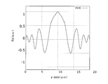
図22は、固有モード計算部21が計算した第2導波路130の固有モード(0次)を示している。また、図23は、モード分布抽出部31が、図15に示す第2導波路130の参照区間Iにおいて定義された参照面aでのモード分布を計算した結果を示している。図23に示すモード分布は、y軸方向のモード分布の代表値を示している。
さらに、図24は、第2導波路130に設定されている参照面aの位置を振って、結合効率計算部41がモード分布に基づいて計算した結合効率と、第2導波路130の距離との関係をプロットした結果を示している。図24の横軸は、z軸に沿った、参照区間Iの右端からの距離D(図14)を示している。また、縦軸は結合効率[dB]を示している。
以上説明したように、本実施の形態に係る解析装置1によれば、0次以上の固有モードが複合した導波路の導波モードを計算し、計算された導波モードを光源として、FDTD法によって、光接続構造の電磁界分布を計算するので、多数の電磁界のモードが複合されている場合であっても、光接続構造を解析することができる。
以上、本発明の解析装置および解析方法における実施の形態について説明したが、本発明は説明した実施の形態に限定されるものではなく、請求項に記載した発明の範囲において当業者が想定し得る各種の変形を行うことが可能である。
1…解析装置、10…設定部、20…求解部、30…データ抽出部、40…特性解析部、50…評価部、11…第1構造設定部、12…第2構造設定部、13…第3構造設定部、21…固有モード計算部、22…導波モード計算部、23…第1分布計算部、24…第2分布計算部、31…モード分布抽出部、32…第1応答計算部、33…第2応答計算部、34…第3応答計算部、41…結合効率計算部、42…反射率計算部、43…透過率計算部、110、110a、110b…光接続構造、120…第1導波路、130…第2導波路、140…光学素子、140b…接着層、141b…レンズ、121,131…コア、122,132…クラッド、101…バス、102…プロセッサ、103…主記憶装置、104…通信インターフェース、105…補助記憶装置、106…I/O装置、107…入力装置、108…表示装置。
Claims (8)
- 光接続構造の構造に関する情報を設定する設定部と、
前記光接続構造の前記構造に関する情報に基づいて、前記光接続構造に分布する電磁界を未知数とした偏微分方程式を求解して前記電磁界の分布を求める求解部と、
前記求解部が求解した前記電磁界の分布から、前記光接続構造の所定の位置における面内でのモード分布、および前記光接続構造の所定の位置での電磁界の時間応答を抽出するデータ抽出部と、
前記データ抽出部が抽出した前記モード分布および前記電磁界の時間応答に基づいて、前記光接続構造に関する光学的な特性を解析する特性解析部と
を備える解析装置。 - 請求項1に記載の解析装置において、
前記光接続構造は、第1導波路および第2導波路と、前記第1導波路と前記第2導波路とを互いに光学的に接続する光学素子とを含み、
前記求解部は、
前記第1導波路に対し、前記光学素子側の端面での反射が発生しない場合において、0次以上の固有モードが複合した電磁界を示す導波モードを計算する導波モード計算部と、
前記導波モードに基づいて、前記光接続構造に含まれる領域の電磁界の分布を計算する第1分布計算部と、
前記第1導波路から前記第2導波路に向かって電磁波が伝搬したときの前記第1導波路および前記光学素子に含まれる領域の電磁界の分布を示す基準電界の分布を計算する第2分布計算部と
を有することを特徴とする解析装置。 - 請求項2に記載の解析装置において、
前記求解部は、
前記第2導波路の固有モードを計算する固有モード計算部を有し、
前記データ抽出部は、
前記第2導波路の光軸と交差する任意の断面内におけるモード分布を抽出するモード分布抽出部を有し、
前記特性解析部は、
前記固有モード計算部によって計算された前記固有モードと、前記モード分布抽出部によって抽出された前記モード分布とに基づいて、前記固有モードと前記モード分布との結合効率を計算する結合効率計算部を有する
ことを特徴とする解析装置。 - 請求項3に記載の解析装置において、
前記データ抽出部は、
前記第1分布計算部が計算した前記電磁界の分布から、前記光学素子の光軸と交差する位置に設定された第1参照座標での電界の時間変化を求める第1応答計算部と、
前記第1分布計算部が計算した前記電磁界の分布から、前記第2導波路の光軸と交差する位置に設定された第2参照座標での電界の時間変化を求める第2応答計算部と、
前記第2分布計算部が計算した前記基準電界の分布から、前記第1参照座標での基準電界の時間変化を求める第3応答計算部と
を有することを特徴とする解析装置。 - 請求項4に記載の解析装置において、
前記特性解析部は、
前記第1応答計算部が求めた前記第1参照座標での電界の時間変化と、前記第3応答計算部が求めた前記基準電界の時間変化とに基づいて、前記第1参照座標での反射率を計算する反射率計算部を有する
ことを特徴とする解析装置。 - 請求項4または請求項5に記載の解析装置において、
前記特性解析部は、
前記第2応答計算部が求めた前記第2参照座標での電界の時間変化と、前記第3応答計算部が求めた前記基準電界の時間変化とに基づいて、前記第2参照座標での透過率を計算する透過率計算部を有する
ことを特徴とする解析装置。 - 請求項1から6のいずれか1項に記載の解析装置において、
前記特性解析部が解析した前記光接続構造に関する光学的な特性から、予め設定された光学的な特性に基づいて、前記設定部が設定した前記光接続構造の構造を評価する評価部をさらに備えることを特徴とする解析装置。 - 光接続構造の構造に関する情報を設定する第1ステップと、
前記光接続構造の前記構造に関する情報に基づいて、前記光接続構造に分布する電磁界を未知数とした偏微分方程式を求解して前記電磁界の分布を求める第2ステップと、
前記第2ステップで求解された前記電磁界の分布から、前記光接続構造の所定の位置における面内でのモード分布、および前記光接続構造の所定の位置での電磁界の時間応答を求める第3ステップと、
前記第3ステップで求められた前記モード分布および前記電磁界の時間応答に基づいて、前記光接続構造に関する光学的な特性を解析する第4ステップと
を備える解析方法。
Priority Applications (1)
| Application Number | Priority Date | Filing Date | Title |
|---|---|---|---|
| US17/421,488 US12050147B2 (en) | 2019-02-22 | 2020-02-07 | Analysis device and analysis method |
Applications Claiming Priority (2)
| Application Number | Priority Date | Filing Date | Title |
|---|---|---|---|
| JP2019030267A JP7103268B2 (ja) | 2019-02-22 | 2019-02-22 | 解析装置および解析方法 |
| JP2019-030267 | 2019-02-22 |
Publications (1)
| Publication Number | Publication Date |
|---|---|
| WO2020170862A1 true WO2020170862A1 (ja) | 2020-08-27 |
Family
ID=72144883
Family Applications (1)
| Application Number | Title | Priority Date | Filing Date |
|---|---|---|---|
| PCT/JP2020/004858 Ceased WO2020170862A1 (ja) | 2019-02-22 | 2020-02-07 | 解析装置および解析方法 |
Country Status (3)
| Country | Link |
|---|---|
| US (1) | US12050147B2 (ja) |
| JP (1) | JP7103268B2 (ja) |
| WO (1) | WO2020170862A1 (ja) |
Families Citing this family (5)
| Publication number | Priority date | Publication date | Assignee | Title |
|---|---|---|---|---|
| WO2020250310A1 (ja) * | 2019-06-11 | 2020-12-17 | 日本電信電話株式会社 | 光パルス試験方法及び光パルス試験装置 |
| JP7643968B2 (ja) * | 2021-07-26 | 2025-03-11 | 株式会社東海理化電機製作所 | 操作検出装置 |
| JP7827610B2 (ja) | 2022-12-16 | 2026-03-10 | 三星電子株式会社 | 算出装置及び算出方法 |
| EP4421700A1 (en) * | 2023-02-24 | 2024-08-28 | Bull Sas | Method for migrating a customer communication document between customer communication management platforms |
| CN116992730B (zh) * | 2023-08-07 | 2024-07-19 | 西安电子科技大学 | 一种矩形波导凋落模电磁特性求解方法 |
Citations (3)
| Publication number | Priority date | Publication date | Assignee | Title |
|---|---|---|---|---|
| JP2001264556A (ja) * | 2000-03-21 | 2001-09-26 | Nippon Telegr & Teleph Corp <Ntt> | 三次元ビーム伝搬法およびその方法を実施するプログラムを記録した記録媒体 |
| JP2013007746A (ja) * | 2011-06-24 | 2013-01-10 | Samsung Electronics Co Ltd | 電磁波解析装置及びその解釈方法 |
| CN104166182A (zh) * | 2014-08-25 | 2014-11-26 | 北京大学 | 一种波导模式转换器 |
-
2019
- 2019-02-22 JP JP2019030267A patent/JP7103268B2/ja active Active
-
2020
- 2020-02-07 US US17/421,488 patent/US12050147B2/en active Active
- 2020-02-07 WO PCT/JP2020/004858 patent/WO2020170862A1/ja not_active Ceased
Patent Citations (3)
| Publication number | Priority date | Publication date | Assignee | Title |
|---|---|---|---|---|
| JP2001264556A (ja) * | 2000-03-21 | 2001-09-26 | Nippon Telegr & Teleph Corp <Ntt> | 三次元ビーム伝搬法およびその方法を実施するプログラムを記録した記録媒体 |
| JP2013007746A (ja) * | 2011-06-24 | 2013-01-10 | Samsung Electronics Co Ltd | 電磁波解析装置及びその解釈方法 |
| CN104166182A (zh) * | 2014-08-25 | 2014-11-26 | 北京大学 | 一种波导模式转换器 |
Non-Patent Citations (2)
| Title |
|---|
| FEND N N ET AL.: "A Hybrid Time-Domain Technique for Simulation of High-Density Integrated Optical Circuits", IEEE JOURNAL OF SELECTED TOPICS IN QUANTUM ELECTRONICS, vol. 11, no. 2, April 2005 (2005-04-01), pages 452 - 456, XP011131079, DOI: 10.1109/JSTQE.2005.846536 * |
| SHIRAISHI, K. ET AL.: "A Micro Light-Beam Spot- Size Converter Using a Hemicylindrical GRIN-Slab Tip With High-Index Contrast", JOURNAL OF LIGHTWAVE TECHNOLOGY, vol. 23, no. 11, November 2005 (2005-11-01), pages 3821 - 3826, XP055735020 * |
Also Published As
| Publication number | Publication date |
|---|---|
| US20220065741A1 (en) | 2022-03-03 |
| US12050147B2 (en) | 2024-07-30 |
| JP2020134386A (ja) | 2020-08-31 |
| JP7103268B2 (ja) | 2022-07-20 |
Similar Documents
| Publication | Publication Date | Title |
|---|---|---|
| JP7103268B2 (ja) | 解析装置および解析方法 | |
| Rahman et al. | Finite element modeling methods for photonics | |
| Khoei et al. | A polygonal finite element method for modeling crack propagation with minimum remeshing | |
| Rivera-Rios et al. | Multi-order vector finite element modeling of 3D magnetotelluric data including complex geometry and anisotropy | |
| Touboul et al. | High-frequency homogenization for periodic dispersive media | |
| Wiltshaw et al. | Analytical solutions for Bloch waves in resonant phononic crystals: deep-subwavelength energy splitting and mode steering between topologically protected interfacial and edge states | |
| CN112231947A (zh) | 一种双各向异性波导的仿真方法及系统 | |
| Pond et al. | Predicting the yield of photonic integrated circuits using statistical compact modeling | |
| CN110673337A (zh) | 一种多芯波导传输特性的快速矢量分析方法 | |
| Dostart et al. | Acoustic waveguide eigenmode solver based on a staggered-grid finite-difference method | |
| Thander et al. | Optical waveguide analysis using alternative direction implicit (ADI) method in combination with successive over-relaxation (SOR) algorithm | |
| Le Cren et al. | A robust 3D crack growth method based on the eXtended Finite Element Method and the Fast Marching Method | |
| Wu et al. | Full-vectorial meshless finite cloud method for an anisotropic optical waveguide analysis | |
| CN110321654A (zh) | 基于MoM与UTD相结合的室内电磁环境预测方法 | |
| Bhattacharyya et al. | Slab waveguide communication study using Finite Difference Method (FDM) with fourth-order compact scheme | |
| Backhaus et al. | Analysis of additive manufactured polymer optical waveguides: measurement and simulation of their waviness | |
| JP6762906B2 (ja) | 電磁界解析方法及び電磁界解析装置 | |
| Avad et al. | A realistic approach for designing a single-mode Y-branch for weakly guiding material system using particle swarm algorithm. | |
| Chen et al. | Parametric simulation of piezoelectric transducer based on finite element method | |
| Bourdine et al. | Method for analysis of real commercially available optical fibers with large core diameter | |
| Darinskii et al. | Acoustic wave degeneracies in two-dimensional phononic crystals | |
| Wu et al. | The Spectral Numerical Mode Matching Method for Simulating Concentric All-Fiber Sensor Structures With Metallic Films | |
| Morozko et al. | Modal theory for twisted waveguides | |
| Hafner et al. | Eigenvalue analysis of lossy dispersive waveguides | |
| JP3693550B2 (ja) | 三次元ビーム伝搬法を用いて三次元光導波路放射モードを導出する方法 |
Legal Events
| Date | Code | Title | Description |
|---|---|---|---|
| 121 | Ep: the epo has been informed by wipo that ep was designated in this application |
Ref document number: 20758794 Country of ref document: EP Kind code of ref document: A1 |
|
| NENP | Non-entry into the national phase |
Ref country code: DE |
|
| 122 | Ep: pct application non-entry in european phase |
Ref document number: 20758794 Country of ref document: EP Kind code of ref document: A1 |