WO2020166681A1 - 面光源装置および表示装置 - Google Patents
面光源装置および表示装置 Download PDFInfo
- Publication number
- WO2020166681A1 WO2020166681A1 PCT/JP2020/005690 JP2020005690W WO2020166681A1 WO 2020166681 A1 WO2020166681 A1 WO 2020166681A1 JP 2020005690 W JP2020005690 W JP 2020005690W WO 2020166681 A1 WO2020166681 A1 WO 2020166681A1
- Authority
- WO
- WIPO (PCT)
- Prior art keywords
- light
- emitting element
- light emitting
- source device
- light source
- Prior art date
- Legal status (The legal status is an assumption and is not a legal conclusion. Google has not performed a legal analysis and makes no representation as to the accuracy of the status listed.)
- Ceased
Links
Images




Classifications
-
- F—MECHANICAL ENGINEERING; LIGHTING; HEATING; WEAPONS; BLASTING
- F21—LIGHTING
- F21S—NON-PORTABLE LIGHTING DEVICES; SYSTEMS THEREOF; VEHICLE LIGHTING DEVICES SPECIALLY ADAPTED FOR VEHICLE EXTERIORS
- F21S2/00—Systems of lighting devices, not provided for in main groups F21S4/00 - F21S10/00 or F21S19/00, e.g. of modular construction
-
- F—MECHANICAL ENGINEERING; LIGHTING; HEATING; WEAPONS; BLASTING
- F21—LIGHTING
- F21V—FUNCTIONAL FEATURES OR DETAILS OF LIGHTING DEVICES OR SYSTEMS THEREOF; STRUCTURAL COMBINATIONS OF LIGHTING DEVICES WITH OTHER ARTICLES, NOT OTHERWISE PROVIDED FOR
- F21V5/00—Refractors for light sources
-
- F—MECHANICAL ENGINEERING; LIGHTING; HEATING; WEAPONS; BLASTING
- F21—LIGHTING
- F21V—FUNCTIONAL FEATURES OR DETAILS OF LIGHTING DEVICES OR SYSTEMS THEREOF; STRUCTURAL COMBINATIONS OF LIGHTING DEVICES WITH OTHER ARTICLES, NOT OTHERWISE PROVIDED FOR
- F21V5/00—Refractors for light sources
- F21V5/04—Refractors for light sources of lens shape
-
- F—MECHANICAL ENGINEERING; LIGHTING; HEATING; WEAPONS; BLASTING
- F21—LIGHTING
- F21V—FUNCTIONAL FEATURES OR DETAILS OF LIGHTING DEVICES OR SYSTEMS THEREOF; STRUCTURAL COMBINATIONS OF LIGHTING DEVICES WITH OTHER ARTICLES, NOT OTHERWISE PROVIDED FOR
- F21V7/00—Reflectors for light sources
- F21V7/22—Reflectors for light sources characterised by materials, surface treatments or coatings, e.g. dichroic reflectors
- F21V7/28—Reflectors for light sources characterised by materials, surface treatments or coatings, e.g. dichroic reflectors characterised by coatings
-
- G—PHYSICS
- G02—OPTICS
- G02B—OPTICAL ELEMENTS, SYSTEMS OR APPARATUS
- G02B5/00—Optical elements other than lenses
- G02B5/02—Diffusing elements; Afocal elements
Definitions
- the present invention relates to a surface light source device and a display device.
- a direct type surface light source device may be used as a backlight.
- a direct type surface light source device having a plurality of light emitting elements has been used as a light source.
- the direct type surface light source device has a substrate, a plurality of light emitting elements, a plurality of light flux controlling members (lenses), and a light diffusing member.
- the light emitting element is, for example, a light emitting diode (LED) such as a white light emitting diode.
- the plurality of light emitting elements are arranged in a matrix on the substrate (for example, a plurality of rows including a plurality of light emitting elements are arranged).
- a light flux controlling member that disperses the light emitted from each light emitting element in the surface direction of the substrate is disposed on each light emitting element. The light emitted from the light flux controlling member is diffused by the light diffusing member and illuminates the irradiated member (for example, the liquid crystal panel) in a planar manner.
- the lighting device 12 of Patent Document 1 includes a chassis 22 having an opening on the liquid crystal panel side, an LED 24, a diffusion lens 27, and an absorption lens arranged on an LCD substrate 25 in the chassis 22. It has a layer 31 and an optical member 23 arranged so as to close the opening of the chassis 22.
- the diffusing lens 27 has an entrance surface 27a and exit surfaces 27b and e.
- the absorption layer 31 is arranged in the circular lens insertion hole 29d of the reflection sheet 29, which has a diameter larger than the outer diameter of the diffusion lens 27 on the surface of the LCD substrate 25 (see FIG. 1A).
- the light emitted from the light emitting element is not emitted from the light emitting device that distributes the light emitted from the light emitting element isotropically (in all directions) as shown in FIGS. 2.
- Light-emitting devices that are anisotropically distributed (indicating elliptical light distribution) by reflecting light in two directions opposite to each other are being used.
- some light emitting elements emit light not only from the top surface of the light emitting element, but also from the side surface.
- the light emitted from the side surface of the light emitting element may be more yellowish than the light emitted from the upper surface of the light emitting element due to the uneven distribution of the distribution of the phosphors.
- a surface light source device having the light emitting device has a yellowish color emitted from the side surface of the light emitting element.
- the light is reflected on the substrate in the vicinity of the light emitting element and reaches the light diffusing plate in the vicinity of directly above the light emitting device, and tends to become light with a strong yellow color.
- color unevenness is likely to occur in the surface light source device, and the uniformity of the in-plane chromaticity distribution is likely to deteriorate.
- the present invention has been made in view of the above circumstances, and even when light emitted from the side surface of the light emitting element has a strong yellow tint, a surface light source device and a display capable of reducing color unevenness due to the yellow light
- the purpose is to provide a device.
- a surface light source device is a light-emitting device which has a housing having a bottom plate, an opening arranged to face the bottom plate, and which is arranged on the bottom plate and emits light from at least upper ends of upper and side surfaces.
- a light emitting device having an element and a light flux controlling member for controlling light distribution of light emitted from the light emitting element; a light absorbing portion arranged on the bottom plate below the light flux controlling member; and the opening.
- a light diffusing plate that diffuses and transmits the light, and the light flux controlling member includes an incident surface on which the light emitted from the light emitting element is incident and the incident surface.
- the light absorbing section has a reflecting surface and two emitting surfaces that are arranged to face each other with the two reflecting surfaces sandwiched therebetween and that respectively emit the light reflected by the two reflecting surfaces to the outside.
- the height of the upper end of the side surface of the light emitting element from the surface of the bottom plate is H, the distance from the lower end of the side surface of the light emitting element when viewed in plan is L, and the light is emitted from the upper end of the side surface of the light emitting element.
- the two emission surfaces are Is substantially perpendicular to the facing direction, and in a direction substantially perpendicular to the optical axis of the light emitting element, it is arranged in at least the entire first region satisfying the following formula (1), H/tan(180 ⁇ 2 ) ⁇ L ⁇ H/tan(180 ⁇ 1 ) Formula (1) (In the formula (1), ⁇ 1 is 120° and ⁇ 2 is 150°)
- ⁇ 1 is 120° and ⁇ 2 is 150°
- the reflectance of light having a wavelength of 450 nm is R 450
- the reflectance of light having a wavelength of 550 nm is R 550
- the reflectance of light having a wavelength of 600 nm is R 600
- R 450 , R 550 and R 600 Are 50% or less, and the light absorbing portion satisfies all of the following expressions (2-1)
- the display device includes the surface light source device according to the present invention, and a display member to which the light emitted from the surface light source device is irradiated.
- the present invention it is possible to provide a surface light source device and a display device that can reduce color unevenness caused by light emitted from the side surface of a light emitting element even if the light has a strong yellow tint.
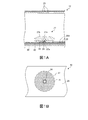
- FIG. 1A and 1B are diagrams showing a configuration of a conventional light emitting device.
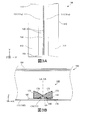
- 2A to 2C are diagrams showing the configuration of the surface light source device according to the present embodiment.
- 3A and 3B are diagrams showing the configuration of the surface light source device according to the present embodiment.
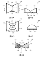
- 4A to 4E are diagrams showing the configuration of the light flux controlling member according to the present embodiment.
- FIG. 5 is a schematic view of the light emitting device of the surface light source device according to the present embodiment as viewed from the back side.
- 6A and 6B are explanatory diagrams showing the region of the light absorbing portion in the present embodiment.
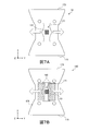
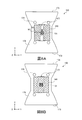
- 7A and 7B are diagrams for explaining the operation.
- FIG. 8A and 8B are schematic views of the light emitting device of the surface light source device according to the modification as viewed from the back side.
- FIG. 9 is a diagram for explaining the shape and size of the light absorbing portion of the surface light source device according to the present embodiment.
- FIG. 10A shows the measurement result of the chromaticity x value on the light diffusion plate of the surface light source device according to the present embodiment and the measurement result of the chromaticity x value on the light diffusion plate of the surface light source device for comparison.
- 10B is a graph
- FIG. 10B is a graph showing measurement results of chromaticity y values on the light diffusion plate of the surface light source device according to the present embodiment, and measurement of chromaticity y values on the light diffusion plate of the surface light source device for comparison. It is a graph which shows a result.
- FIGS. 3A and 3B are diagrams showing the configuration of the surface light source device 100 according to the present embodiment.
- 2A is a plan view of the surface light source device 100
- FIG. 2B is a side view
- FIG. 2C is a front view
- 3A is a plan view with the light diffusion plate 150 removed from FIG. 2A
- FIG. 3B is a partially enlarged cross-sectional view taken along the line AA of FIG. 2A. Note that, in FIG. 3B, the size of the light emitting device 130 is displayed in a large size, and hatching of some members is omitted.
- the surface light source device 100 includes a housing 110, a substrate 120, a plurality of light emitting devices 130, a light absorbing section 140, and a light diffusing plate 150. Further, as shown in FIG. 2C, the surface light source device 100 can also be used as a display device 100 ′ by combining it with a display member (irradiated member) 160 such as a liquid crystal panel.
- a display member irradiated member
- the housing 110 is a box, at least a part of which is opened, for housing the substrate 120 and the plurality of light emitting devices 130 therein, and has a bottom plate 111 and an opening arranged to face the bottom plate 111.
- the housing 110 has a bottom surface 111 a that is the surface of the bottom plate 111, two first inclined surfaces 112, and two second inclined surfaces 113.
- the bottom surface 111a may be a horizontal surface.
- the two first inclined surfaces 112 and the two second inclined surfaces 113 are surfaces that are arranged so as to sandwich the bottom surface 111 a and that are inclined so as to approach the light diffusion plate 150 as the distance from the light emitting element 131 increases.
- the two first inclined surfaces 112 and the two second inclined surfaces 113 reflect the light emitted from the light emitting device 130 in a substantially horizontal direction toward the light diffusion plate 150, so that the light emitted from the light emitting device 130 is reflected. It can be easily collected in the light diffusion plate 150. That is, the first inclined surface 112 and the second inclined surface 113 can each function as a reflecting surface.
- the first inclined surface 112 and the second inclined surface 113 may each be a flat surface or a curved surface. In the present embodiment, both the first inclined surface 112 and the second inclined surface 113 are flat surfaces.
- the inclination angle of the first inclined surface 112 with respect to the bottom surface 111a is, for example, 6 to 9°
- the inclination angle of the second inclined surface 113 with respect to the bottom surface 111a is, for example, 40 to 50°.
- the angle of inclination of the first inclined surface 112 (or the second inclined surface 113) with respect to the bottom surface 111a is the smaller of the angles formed by the first inclined surface 112 (or the second inclined surface 113) and the bottom surface 111a.
- the tilt angle with respect to the bottom surface 111a means the tilt angle with respect to the horizontal portion of the bottom surface 111a.
- the inclination angle of the first inclined surface 112 (or the second inclined surface 113) with respect to the bottom surface 111a is the bottom surface in the first imaginary cross section. It means the smaller one of the angles formed by 111a and the tangent of the curve in the virtual cross section of the first inclined surface 112 (or the second inclined surface 113).
- the housing 110 By forming the housing 110 in such a shape, the apparent thickness of the surface light source device 100 can be reduced.
- the size of the opening of the housing 110 corresponds to the size of the light emitting region formed on the light diffusion plate 150, and is, for example, 400 mm ⁇ 700 mm (32 inches). This opening is closed by the light diffusion plate 150.
- the height (space thickness) from the surface of the bottom surface 111a to the light diffusion plate 150 is not particularly limited, but is about 10 to 40 mm.
- the housing 110 is made of, for example, resin such as polymethylmethacrylate (PMMA) or polycarbonate (PC), metal such as stainless steel or aluminum, or the like.
- the substrate 120 is arranged on the bottom plate 111 (bottom surface 111a) of the housing 100.
- the substrate 120 is a flat plate for arranging the plurality of light emitting devices 130 in the housing 110 at predetermined intervals.
- the surface of the substrate 120 reflects the light reaching from the light emitting device 130 toward the light diffusion plate 150. That is, the surface of the substrate 120 can also function as a reflecting surface.
- the plurality of light emitting devices 130 are substantially perpendicular to the direction (X axis direction) in which two emission surfaces 173 of the light flux controlling member 132, which will be described later, face each other on the substrate 120, and the optical axis LA (Z axis direction) of the light emitting element 131. ) Are arranged in a line along a direction (Y-axis direction) substantially perpendicular to ().
- the number of light emitting devices 130 arranged on the substrate 120 is not particularly limited. The number of the light emitting devices 130 arranged on the substrate 120 is appropriately set based on the size of the light emitting area (light emitting surface) defined by the opening of the housing 110.
- Each of the plurality of light emitting devices 130 has a light emitting element 131 and a light flux controlling member 132.
- the plurality of light emitting devices 130 are arranged such that the optical axis of the light emitting element 131 (the optical axis LA of the light emitting element 131 described later) is along the normal to the surface of the substrate 120, and light emitted from the light emitting element 131.
- the optical axis LA of the light emitting element 131 are arranged so as to be emitted toward the two first inclined surfaces 112, respectively.
- the light emitting element 131 is arranged on the substrate 120.
- the light emitting element 131 is a light source of the surface light source device 100 (and the light emitting device 130), and emits light from the upper ends of the upper surface and the side surface.
- the light emitting element 131 is, for example, a light emitting diode (LED).
- the color of the light emitted from the vicinity of the light emission center of the light emitting element 131 can be set appropriately.
- the color of the light emitted from the vicinity of the emission center of the light emitting element 131 may be white or blue. In the present embodiment, the color of light emitted from the vicinity of the light emission center of light emitting element 131 is white.
- the height of the light emitting surface of the light emitting element 131 is the same as or lower than the back surface 176 of the light flux controlling member 132. Is preferably higher than.
- the light flux controlling member 132 controls the light distribution of the light emitted from the light emitting element 131.
- Light flux controlling member 132 is arranged on light emitting element 131 such that its central axis CA coincides with optical axis LA of light emitting element 131 (see FIG. 3B).
- the “optical axis LA of the light emitting element 131” means the light beam at the center of the three-dimensional light flux emitted from the light emitting element 131.
- the "central axis CA of the light flux controlling member 132" means, for example, a symmetry axis of twofold symmetry.
- light flux controlling member 132 emits light emitted from light emitting element 131 from two emission surfaces 173 described later toward two first inclined surfaces 112 (two emission surfaces 173 described later are described below).
- the two first inclined surfaces 112 are arranged so as to face each other).
- a virtual axis including the light emission center of the light emitting element 131 as an origin, an axis parallel to the optical axis LA of the light emitting element 131 as the Z axis, orthogonal to the Z axis, and including the light emission center of the light emitting element 131
- an axis parallel to the direction in which the plurality of light emitting devices 130 are arranged is a Y axis
- an axis orthogonal to the Y axis is an X axis.
- a cross section of the light emitting device 130 taken along a first virtual plane (XZ plane) including the optical axis LA and the X axis is referred to as a first virtual cross section, and a second virtual plane (YZ) including the optical axis LA and the Y axis is set.
- disconnected by the plane) be a 2nd virtual cross section
- disconnected by the 3rd virtual plane (XY plane) containing an X-axis and a Y-axis be a 3rd virtual cross section.
- light flux controlling member 132 is plane-symmetric with respect to the first virtual plane (XZ plane) and the second virtual plane (YZ plane).
- light flux controlling member 132 is an object of which the optical surfaces (the entrance surface 171, the reflecting surface 172, and the exit surface 173 described later) are substantially rotationally symmetric with the axis parallel to the X axis as the axis of rotation. It is a part.
- the material of light flux controlling member 132 is not particularly limited as long as it can pass light of a desired wavelength.
- the material of light flux controlling member 132 is a light transmissive resin such as polymethylmethacrylate (PMMA), polycarbonate (PC), epoxy resin (EP), or glass.
- PMMA polymethylmethacrylate
- PC polycarbonate
- EP epoxy resin
- glass glass
- the two light absorbing parts 140 are arranged between the light flux controlling member 132 and the substrate 120 (see FIGS. 3B and 6A).
- Light absorbing portion 140 absorbs at least a part of light emitted from the upper end portion of the side surface of light emitting element 131 and reaching the surface of substrate 120 below light flux controlling member 132. Thereby, the light emitted from the upper end portion of the side surface of the light emitting element 131 and reflected on the substrate 120 below the light flux controlling member 132 can be reduced, so that the light diffusing plate 150 in the vicinity immediately above the light emitting device 130 can be used. It is possible to suppress the yellowness of the emitted light from increasing.
- the configuration of the light absorption unit 140 will be described in detail separately.
- the light diffusion plate 150 is arranged so as to close the opening of the housing 110.
- Light diffusing plate 150 is a plate-shaped member having a light transmitting property and a light diffusing property, and transmits the light emitted from light emitting surface 173 of light flux controlling member 132 while diffusing the light.
- the light diffusion plate 150 can be, for example, a light emitting surface of the surface light source device 100.
- the material of the light diffusion plate 150 can be appropriately selected as long as it can diffuse and transmit the light emitted from the light emitting surface 173 of the light flux controlling member 132.
- Examples of the material of the light diffusion plate 150 include light transmissive resins such as polymethylmethacrylate (PMMA), polycarbonate (PC), polystyrene (PS), and styrene-methylmethacrylate copolymer resin (MS).
- PMMA polymethylmethacrylate
- PC polycarbonate
- PS polystyrene
- MS styrene-methylmethacrylate copolymer resin
- the light diffusing plate 150 has fine irregularities formed on its surface, or light diffusing elements such as beads are dispersed inside the light diffusing plate 150.
- the light emitted from each light emitting element 131 is directed specifically toward the first inclined surface 112 so that the light flux controlling member 132 illuminates a wide range of the light diffusing plate 150 (or The light is emitted after being changed in a direction substantially perpendicular to the optical axis LA of the light emitting element 131 and in two directions (X-axis directions in FIG. 3A) that are substantially opposite to each other.
- the light emitted from each light flux controlling member 132 is further diffused by the light diffusion plate 150 and emitted to the outside. Thereby, light can be spread over the entire surface of the surface light source device 100.
- FIG. 4A to 4E are diagrams showing the configuration of light flux controlling member 132.
- 4A is a plan view of light flux controlling member 132
- FIG. 4B is a front view
- FIG. 4C is a bottom view
- FIG. 4D is a side view
- FIG. 4E is shown in FIG. 4A. It is a sectional view taken along the line AA.
- the substrate 120 side (light emitting element 131 side) is referred to as “back side”
- the light diffusion plate 150 side is referred to as “front side”.
- the light flux controlling member 132 controls the light distribution of the light emitted from the light emitting element 131. As shown in FIGS. 4A to 4E, light flux controlling member 132 has entrance surface 171, two reflecting surfaces 172, two exit surfaces 173, two flanges 174, and four legs 175.
- the incident surface 171 allows the light emitted from the light emitting element 131 to enter.
- Incident surface 171 is arranged on the back side (light emitting element 131 side, rear surface 176) of light flux controlling member 132 so as to intersect optical axis LA.
- the shape of the incident surface 171 is not particularly limited as long as it can exhibit the above function.
- the shape of the incident surface 171 may be a flat surface, or may be the inner surface of the concave portion 177 opened on the back surface 176. In the present embodiment, the incident surface 171 is the inner surface of the recess 177 that is open in the back surface 176.
- the shape of the recess 177 is also not particularly limited.
- the recess 177 has an inner top surface 177a (first incident surface) and an inner side surface 177b (second incident surface) that is opposed to the inner top surface 177a in the X-axis direction.
- the numbers of the inner top surface 177a (first incident surface) and the inner side surfaces 177b (second incident surface) are not particularly limited, and may be one each, or may be two or more. In the present embodiment, the numbers of the inner top surface 177a and the inner side surface 177b are each two.
- the inner top surface 177a (first incident surface) and the inner side surface 177b (second incident surface) may be flat surfaces or curved surfaces.
- the inner top surface 177a is a curved surface that is convex on the back side in the first imaginary cross section from the viewpoint of making it easier for the incident light to reach the reflecting surface 172
- the inner side surface 177b is a flat surface.
- the inner surface (incident surface 171) of the recess 177 may further have another surface.
- the two reflecting surfaces 172 are arranged at positions (front side) facing the light emitting element 131 with the entrance surface 171 interposed therebetween. Further, the two reflecting surfaces 172 have two directions in which at least a part of the light incident on at least the inner top surface 177a is substantially perpendicular to the optical axis LA of the light emitting element 131 and is substantially opposite to each other (both are in the opposite directions). It is reflected in the direction along the X axis). The two reflecting surfaces 172 are formed so as to separate from the X-axis as they separate from the optical axis LA in the first virtual cross section.
- the two reflection surfaces 172 are tangential lines from the optical axis LA of the light emitting element 131 toward the end (emission surface 173) in the cross section (first virtual cross section) including the optical axis LA of the light emitting element 131. Are formed so as to gradually decrease in inclination (along the X axis).
- the two emitting surfaces 173 are arranged to face each other (in the X-axis direction) with the two reflecting surfaces 172 interposed therebetween.
- the two emission surfaces 173 respectively enter the light incident on the inner top surface 177a and reflected on the reflection surface 172 and the light incident on the inner surface 177b and directly reaching the outside (the first inclined surface of the housing 110). (Toward 112).
- the emission surface 173 may be a flat surface or a curved surface.
- the emission surface 173 is a surface that is substantially parallel to the optical axis LA in the first virtual cross section (or a plane that is parallel to the second virtual cross section).
- substantially parallel to the optical axis LA means that the smaller one of the angles formed by the optical axis LA and the emission surface 173 is 3° or less in the first virtual cross section.
- the emission surface 173 is a curved surface, the smaller angle of the angles formed by the optical axis LA and the emission surface 173 is the first virtual cross section of the optical axis LA and the emission surface 173. The smaller angle among the angles formed by the tangents of the curve in the cross section.
- the two flange portions 174 are arranged between the two reflecting surfaces 172 near the optical axis LA so as to project in the Y-axis direction with respect to the optical axis LA. Collar 174 facilitates handling and alignment of light flux controlling member 132.
- the shape of the collar portion 174 may be such that the light incident on the collar portion 174 can be controlled and emitted.
- the four legs 175 are substantially columnar members protruding from the back surface 176.
- the leg portion 175 supports the light flux controlling member 132 at an appropriate position with respect to the light emitting element 131 (see FIG. 3B).
- the legs 175 may be fitted into the holes formed in the substrate 120 and used for positioning. Further, leg portions 175 are only required to be able to stably fix light flux controlling member 132 to substrate 120 after taking into consideration no optical adverse effects, and the position, shape and number of leg portions 175 are particularly limited. Not done.
- a total of four leg portions 175 are arranged on the back surface 176 around the entrance surface 171.
- the edge portion where the surfaces are in contact with each other may have a slight R shape on the product in terms of mold making, molding, or optical characteristics.
- R0 perfect edge
- the portion directly above the light emitting device 130 becomes dark, and therefore the curvature is compensated for to compensate for the brightness. It is preferable to provide an R shape having a radius R of about 0.05 to 0.07 mm.
- FIG. 5 is a schematic view of the light emitting device 130 of the surface light source device 100 according to the present embodiment as viewed from the back side (the substrate 120 side).
- 6A and 6B are partially enlarged cross-sectional views around the light emitting device 131 of FIG. 3B.
- the two light absorbing portions 140 are arranged on the substrate 120 with the light emitting element 131 interposed therebetween in at least a direction (Y-axis direction) substantially perpendicular to the direction in which the two emission surfaces 173 of the light flux controlling member 132 face each other. ing.
- two light absorption portions 140 are arranged in a direction (Y-axis direction) substantially perpendicular to the direction in which two emission surfaces 173 of light flux controlling member 132 face each other with light emitting element 131 interposed therebetween. Further, they are not arranged in at least a part of the direction (X-axis direction) substantially parallel to the direction in which the two emission surfaces 173 of the light flux controlling member 132 face each other.
- the light emitted from the upper end portion of the side surface of the light emitting element 131 the light emitted in the direction (Y-axis direction) substantially perpendicular to the direction in which the two emission surfaces 173 of the light flux controlling member 132 face each other.
- the light flux controlling member 132 is not sufficiently diffused and easily leaks to the outside.
- the yellow color of the light emitted from the light diffusing plate 150 immediately above the light emitting device 130 tends to be stronger.
- the light absorbing section 140 is arranged on the substrate 120 at least in the Y-axis direction with the light emitting element 131 interposed therebetween.
- the light reflected on the substrate 120 is not diffused by the light flux controlling member 132 but leaked to the outside can be reduced.
- the yellowish color of the light emitted from immediately above the light emitting device 130 from increasing.
- the height of the upper end of the side surface of the light emitting element 131 from the surface of the substrate 120 is H
- the distance from the lower end of the side surface of the light emitting element 131 in a plan view is L
- the side surface of the light emitting element 131 is
- the angle of the light emitted from the upper end with respect to the reference line that passes through the upper end of the side surface of the light emitting element 131 and extends to the light diffusion plate 150 in parallel with the optical axis LA of the light emitting element 131 is ⁇ ( ⁇ 1 ⁇ 2 )
- the light absorption portion 140 is arranged in the entire first region 120a on the substrate 120 that satisfies the following expression (1) in the Y-axis direction (see FIG. 6A). That is, the light absorbing section 140 is arranged in a region including the first region 120a.
- the “height H from the surface of the bottom plate (at the upper end of the side surface of the light emitting element)” in the present invention is “ “Height from the surface of the substrate 120 (of the upper end portion of the side surface of the light emitting element)”.
- the surface of the substrate 120 (or the bottom surface 111a) is perpendicular to the optical axis LA of the light emitting element 131, “the light emitting element 131 (of the light emitted from the upper end portion of the side surface of the light emitting element) of the present invention is used.
- the "distance L from the lower end of the side surface of the light emitting element (when viewed in a plan view)" in the present invention means "the distance from the lower end of the side surface of the light emitting element 131 in the direction along the bottom surface 111a".
- the height H of the upper end of the side surface of the light emitting element 131 from the surface of the substrate 120 depends on the type of the light emitting element 131, but may be, for example, 0.2 to 2 mm.
- An angle ⁇ of the light emitted from the upper end portion of the side surface of the light emitting element 131 with respect to the normal line of the substrate 120 indicates a polar angle with respect to the normal line of the substrate 120 (see FIG. 6A). Specifically, the light is emitted from the upper end of the side surface of the light emitting element 131 when the direction toward the light diffusion plate 150 along the normal direction of the substrate 120 is 0°.
- Angle of light ⁇ 1 is preferably 120° and ⁇ 2 is preferably 150°.
- the first region 120a satisfying the formula (1) is light emitted from the upper end portion of the side surface of the light emitting element 131 at an angle (polar angle) of ⁇ 1 or more and ⁇ 2 or less with respect to the normal line of the surface of the substrate 120. Indicates the region where the surface reaches the surface of the substrate 120.
- the light absorbing section 140 By disposing the light absorbing section 140 in such a region, it is possible to reduce the light emitted from the upper end portion of the side surface of the light emitting element 131 and reflected on the substrate 120. As a result, it is possible to prevent the light emitted from the light diffusing plate 150 immediately above the light emitting device 130 from becoming more yellowish.
- the light absorbing portion 140 absorbs more of the light emitted from the upper end portion of the side surface of the light emitting element 131 and reaching the substrate 120, and from the viewpoint of making it more difficult to generate light with a strong yellowish color, ⁇ 5 ⁇
- the light absorbing portion 140 is represented by the following formula (3) in addition to the above-described first region 120 a. It is preferable that the third region 120c and the fourth region 120d represented by the following formula (4) are all further arranged (see FIG. 6B).
- the light absorbing section 140 includes, in at least the Y-axis direction, the fifth region 120e represented by the following formula (5) and the following formula in addition to the above-described first region 120a, the third region 120c, and the fourth region 120d. It is more preferable that the sixth region 120f represented by (6) is further arranged in all of at least one side (see FIG. 6B).
- the light absorbing portion 140 includes the first region 120a.
- the fourth region 120d (which is closer to the light emitting element 131 than that) in addition to the first region 120a and the fourth region 120d. More preferably, it is arranged in a region further including (close) the sixth region 120f.
- the outer edge of the light absorbing section 140 is preferably inside the outer edge of the light flux controlling member 132.
- the light absorption unit 140 has a reflectance of light having a wavelength of 450 nm as R 450 , a reflectance of light having a wavelength of 550 nm as R 550 , and a reflectance of light having a wavelength of 600 nm as R 600 , the light absorption unit 140 has the following formula (2-1) to (2-3) are all satisfied.
- 0.5 ⁇ r 1 ⁇ 1, r 1 R 550 /R 450 Formula (2-1)
- the reflectance on the long wavelength side (for example, yellow region) is made lower than the reflectance on the short wavelength side (for example, blue region). That is, the ratio of R 550 to the reflectance R 450 (r 1 ), the ratio of R 600 to R 450 (r 2 ), and the ratio of R 550 to R 600 (r 3 ) of the light absorbing portion 140 are respectively appropriate.
- the light absorption part 140 can absorb the light particularly on the long wavelength side of the light emitted from the upper end portion of the side surface of the light emitting element 131 and reaching the substrate 120.
- the long-wavelength side light of the light emitted from the upper end portion of the side surface of the light emitting element 131 and reaching the substrate 120 cannot be sufficiently absorbed, and thus yellow This may result in a palatable reflected light.
- the light absorbing section 140 cannot sufficiently absorb the light on the short wavelength side of the light reaching the substrate 120, and may generate bluish reflected light. is there.
- r 1 and r 2 are 0.6 ⁇ r 1, r It is preferable that 2 ⁇ 0.9 is satisfied, and it is more preferable that 0.7 ⁇ r 1 and r 2 ⁇ 0.8 are satisfied. Further, if r 3 is too large, the reflected light due to the light reaching the substrate 120 tends to have a greenish tint, and if r 3 is too small, the reflected light due to the light reaching the substrate 120 has a reddish tint. Therefore, r 3 preferably satisfies 0.9 ⁇ r 3 ⁇ 1.1, and 0.95 ⁇ r 3 ⁇ 1.05. Is more preferable.
- the reflectances R 450 , R 550, and R 600 of the light absorbing portion 140 are preferably low from the viewpoint of further increasing the absorption efficiency of light emitted from the upper end portion of the side surface of the light emitting element 131, and specifically, , 50% or less, preferably 40% or less, and more preferably 30% or less.
- the light emitted from the side surface of the light emitting element 131 is reflected on the substrate 120, and the yellowish color of the light emitted from the light diffusion plate 150 near the portion directly above the light emitting device 130 is suppressed. be able to.
- the reflectances R 450 , R 550 and R 600 can be measured according to JIS 8722 (2009). Specifically, the reflectance of light at a wavelength of 450 nm, 550 nm, or 600 nm is measured at an incident angle of 45° using a spectrophotometer. The measurement is performed in the wavelength range of 400 to 700 nm.
- the light absorbing section 140 has an L value (brightness) in the Lab color system that corresponds to the side surface of the light emitting element 131. From the viewpoint of further increasing the absorption efficiency of the light emitted from the upper end of the above, it is preferably low, and specifically, it is preferably 40 or less.
- the L value (brightness) can be measured using a spectrophotometer according to JIS 8781-4 (2013) (CIE 1976L * a * b * color space).
- the reflectance R 450 , R 550 and R 600 of the light absorbing portion 140 and the L value can be adjusted by the hue of the light absorbing portion 140 and the like.
- the hue of the light absorbing portion 140 is preferably black.
- the light absorbing section 140 may be a colored layer (preferably a black layer) formed on the surface of the substrate 120 by coating or transfer.
- FIG. 7A is a diagram for explaining the operation of the surface light source device 10 for comparison
- FIG. 7B is a diagram for explaining the operation of the surface light source device 100 according to the present embodiment.
- the surface light source device 10 for comparison has the same configuration as the surface light source device 100 according to the present embodiment, except that the light absorbing portion 140 is not provided on the substrate 120.
- the light emitted from the light emitting element 131 is incident on the incident surface 171 (see FIGS. 3B and 4E).
- a part of the light incident on the incident surface 171 (for example, the light incident on the inner top surface 177a) is reflected by the two reflecting surfaces 172, is substantially perpendicular to the optical axis LA of the light emitting element 131, and is substantially opposite to each other. Proceed in two directions (directions toward the first inclined surface 112) that are the directions, and reach the two emission surfaces 173.
- the light emitted from the light emitting element 131 includes not only the light emitted from the upper surface of the light emitting element 131 but also the light emitted from the upper end portion of the side surface of the light emitting element 131.
- the surface light source device 10 for comparison does not have a light absorbing portion on the substrate 120 (see FIG. 7A). Therefore, of the light emitted from the upper end portion of the side surface of the light emitting element 131, a part of the light emitted in the Y-axis direction is directly reflected on the substrate 120 and then enters the light flux controlling member 132. The light is not sufficiently diffused and easily leaks to the outside of the light flux controlling member 132 as it is (solid arrow in FIG. 7A).
- surface light source device 100 absorbs two light beams on substrate 120 in the direction (Y-axis direction) substantially perpendicular to the direction in which two emission surfaces 173 of light flux controlling member 132 face each other. It has a section 140 (see FIG. 7B). As a result, of the light emitted from the upper end portion of the side surface of the light emitting element 131, most of the light emitted in the Y-axis direction and reaching the substrate 120 is absorbed by the light absorbing portion 140.
- FIGS. 8A and 8B are schematic views of the light emitting device of the surface light source device according to the modification as viewed from the back side.
- the light absorbing parts 240 and 340 are arranged in the above-described formula (X-axis direction) in a direction substantially parallel to the direction in which the two emission surfaces 173 of the light flux controlling member 132 face each other. It may be further arranged in at least a part of the second region which satisfies 1).
- Light absorbing parts 240 and 340 have at least one of the second regions that satisfy the above-mentioned formula (1) in a direction (X-axis direction) substantially parallel to the direction in which two emission surfaces 173 of light flux controlling member 132 face each other. Not only the part, but also at least a part of at least one of the third region 120c satisfying the formula (3) and the fourth region 120d satisfying the formula (4) (preferably the fourth region 120d satisfying the formula (4)). Or at least a part of at least one of the fifth region 120e satisfying the formula (5) and the sixth region 120f satisfying the formula (6) (preferably the sixth region 120f satisfying the formula (6)). May be further arranged.
- the light absorption section 240 is arranged only in a part of the second region on the side closer to the light emitting element 131, and is not arranged on a part of the side distant from the light emitting element 131.
- the part on the side closer to the light emitting element 131 is closer to the light emitting element 131 than the point of half the distance between the light emitting element 131 and the incident surface 171 (inner side surface 177b) of the light flux controlling member 132 in the X-axis direction.
- Part of the side farther from the light emitting element 131 means a region farther from the light emitting element 131 than a half point of the distance between the light emitting element 131 and the incident surface 171 (inner side surface 177b) of the light flux controlling member 132.
- the maximum width W2 of the light absorbing section 240 in the X axis direction from the side surface of the light emitting element 131 is shorter than the maximum width W1 of the light absorbing element 240 in the Y axis direction from the side surface. It is preferable.
- the light emitted in the X-axis direction (the direction in which the two emission surfaces 173 face each other) is absorbed by the light absorption portion 240 on the substrate 120. Since the light is not excessively diffused, it is possible to suppress a decrease in the light diffused inside the light flux controlling member 132 and a decrease in the brightness of the surface light source device.
- planar shape of the light absorbing section 140 is a rectangular shape
- the shape is not limited to this, and may be any shape including a region that satisfies Expression (1).
- the plan view shape of the light absorption section 140 may be a shape that spreads radially from the four corners of the light emitting element 131.
- light emitting device 130 is arranged on substrate 120
- the present invention is not limited to this, and light emitting device 130 may be arranged directly on bottom plate 111.
- Light emitting element 131 may be arranged on substrate 120
- light flux controlling member 132 may be arranged on bottom plate 111.
- first inclined surface 112 and the second inclined surface 113 of the housing 110 function as the reflecting surface
- the present invention is not limited to this, and the first inclined surface 112 and the second inclined surface are not limited thereto.
- a reflection sheet may be further arranged on the surface of the surface 113, and the surface may function as a reflection surface.
- the chromaticity (x, y values) on the light diffuser plate 150 of the surface light source devices A-1 to A-3 according to the present embodiment having different shapes of the light absorbing portions were measured.
- the chromaticity (x, y value) was measured using the surface light source device 100 having only one light emitting device 130.
- the chromaticity (x, y values) on the light diffusion plate of the surface light source device R which is the same as the surface light source devices A-1 to A-3 except that it does not have a light absorbing portion, was also measured.
- the measurement conditions were set as follows.
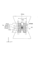
- FIG. 9 is a diagram for explaining the shape and size of the light absorbing portions of the surface light source devices A-1 to A-3 according to the present embodiment.
- the shape and size of the light absorbing portions of the surface light source devices A-1 to A-3 are set as shown in FIG. 9 and as follows.
- Outer diameter of light flux controlling member 132 length in X-axis direction 18.0 mm Length in Y-axis direction 14.3 mm ⁇ Height of light emitting element 131: 0.60 mm ⁇ Size of light emitting element 131: 1.4 mm ⁇ 1.4 mm -Gap between the substrate 120 and the light diffusion plate 150: 29 mm
- FIG. 10A shows the measurement results of the chromaticity x value on the light diffusion plate 150 of the surface light source devices A-1 to A-3 according to the present embodiment, and the light diffusion plate 150 of the surface light source device R for comparison. It is a graph which shows the measurement result of chromaticity x value above. 10A, the horizontal axis represents the position (mm) in the Y-axis direction from the optical axis LA of the light emitting element 131 in the light diffusion plate 150, and the vertical axis represents the chromaticity x value in the light diffusion plate 150. .. FIG.
- 10B shows measurement results of chromaticity y values on the light diffuser plate 150 of the surface light source devices A-1 to A-3 according to the present embodiment, and the light diffuser plate 150 of the surface light source device R for comparison. It is a graph which shows the measurement result of the chromaticity y value above. 10B, the horizontal axis represents the position (mm) in the Y-axis direction from the optical axis LA of the light emitting element 131 in the light diffusion plate 150, and the vertical axis represents the chromaticity y value in the light diffusion plate 150. ..
- the difference between the value (or y value) and the chromaticity x value (or y value) on the light diffusion plate 150 of the surface light source device R for comparison is shown.
- the average value of (value) is shown.
- ⁇ ave(x) is the average value of the chromaticity x values (or y values) of the surface light source devices A-1 to A-3 according to the present embodiment in the above range.
- the difference with the average value of the chromaticity x value (or y value) of the surface light source device R for comparison is shown.
- the surface light source device having the light flux controlling member according to the present invention can be applied to, for example, a backlight of a liquid crystal display device, a signboard, or general lighting.
Landscapes
- Engineering & Computer Science (AREA)
- General Engineering & Computer Science (AREA)
- Physics & Mathematics (AREA)
- General Physics & Mathematics (AREA)
- Optics & Photonics (AREA)
- Planar Illumination Modules (AREA)
- Optical Elements Other Than Lenses (AREA)
- Liquid Crystal (AREA)
Abstract
面光源装置は、筐体、発光装置、光吸収部、および光拡散板を有する。発光装置は、発光素子および光束制御部材を有する。光束制御部材は、入射面、2つの反射面、および2つの出射面を有する。光吸収部は、2つの出射面が対向する方向に略垂直かつ発光素子の光軸に略垂直な方向において、少なくともH/tan(180-θ2)≦L≦H/tan(180-θ1)(θ1:120°以上、θ2:150°以下)を満たす第1領域の全部に配置され、R450、R550およびR600は、それぞれ50%以下であり、かつ0.5≦r1<1、0.5≦r2<1、および0.85≦r3≦1.15を満たす。
Description
本発明は、面光源装置および表示装置に関する。
液晶表示装置などの透過型画像表示装置では、バックライトとして直下型の面光源装置を使用することがある。近年、光源として複数の発光素子を有する、直下型の面光源装置が使用されるようになってきている。
たとえば、直下型の面光源装置は、基板、複数の発光素子、複数の光束制御部材(レンズ)および光拡散部材を有する。発光素子は、例えば白色発光ダイオードなどの発光ダイオード(LED)である。複数の発光素子は、基板上に、マトリクス状に配置(例えば複数の発光素子を含む列が複数列配置)されている。各発光素子の上には、各発光素子から出射された光を基板の面方向に拡げる光束制御部材が配置されている。光束制御部材から出射された光は、光拡散部材により拡散され、被照射部材(例えば液晶パネル)を面状に照らす。
図1AおよびBは、特許文献1の照明装置12(面光源装置)の構成を示す図である。図1AおよびBに示されるように、特許文献1の照明装置12は、液晶パネル側が開口したシャーシ22と、シャーシ22内のLCD基板25上に配置された、LED24と、拡散レンズ27と、吸収層31と、シャーシ22の開口部を塞ぐように配置された光学部材23とを有する。拡散レンズ27は、入射面27aと、出射面27bおよびeとを有する。吸収層31は、LCD基板25の表面のうち、拡散レンズ27の外径よりも大きい径を有する、反射シート29の円形状のレンズ挿通孔29d内に配置されている(図1A参照)。
特許文献1の照明装置12では、LED24から出射された光の多くは、拡散レンズ27の入射面27aで入射し、出射面27bおよびeから出射される。このとき、LED24から出射される光の一部は、拡散レンズ27の裏面で反射されて、LED基板25側に戻る。このように、拡散レンズ27の裏面で反射されて、LED基板25側に戻る光は、LED基板25上に配置された吸収層31によって吸収されるため、LED24の近傍がその他の部分よりも明るくなりすぎないようにし、輝度ムラを低減することができるとされている。
近年では、大型の面光源装置を安価に製造する観点から、発光素子の数を少なくすること(例えば複数の発光素子を含む列の数を少なくすること)が求められている。すなわち、複数の発光素子を含む列の数を少なくしても、面光源装置の隅々まで光を到達させることが求められている。これに伴い、発光素子から出射される光を、図1AおよびBに示されるような等方的に(全方向に)配光させる発光装置ではなく、発光素子から出射される光を、水平方向で互いに反対向きである2つの方向に反射させて、異方的に配光させる(楕円配光を示す)発光装置が使用されつつある。
また、発光素子としては、発光素子の上面からだけでなく、側面からも光を出射するものがある。そのような発光素子では、蛍光体の存在分布の偏りなどに起因して、発光素子の側面から出射される光は、発光素子の上面から出射される光よりも黄色味が強いことがある。
そのような発光素子を、異方的に配光させる(楕円配光を示す)発光装置に用いると、当該発光装置を有する面光源装置では、発光素子の側面から出射された黄色味を帯びた光が、発光素子近傍の基板上で反射されて、発光装置の直上近傍の光拡散板に到達し、黄色味の強い光となりやすいという問題があった。それにより、面光源装置において色ムラを生じやすく、面内色度分布の均一性が低下しやすいという問題があった。
本発明は上記事情を鑑みてなされたものであり、発光素子の側面からの出射される光の黄色味が強い場合であっても、それによる色ムラを低減することができる面光源装置および表示装置を提供することを目的とする。
本発明に係る面光源装置は、底板と、前記底板と対向して配置された開口部とを有する筐体と、前記底板上に配置され、少なくとも上面および側面の上端部から光を出射する発光素子と、前記発光素子から出射された光の配光を制御する光束制御部材とを有する発光装置と、前記底板上の、前記光束制御部材の下に配置された光吸収部と、前記開口部を塞ぐように配置され、光を拡散させつつ透過させる光拡散板と、を有し、前記光束制御部材は、前記発光素子から出射された光を入射する入射面と、前記入射面を挟んで前記発光素子と対向する位置に配置され、前記入射面から入射した光の一部を、前記発光素子の光軸と略垂直であり、かつ互いに反対向きである2つの方向にそれぞれ反射させる2つの反射面と、前記2つの反射面を挟んで互いに対向して配置され、前記2つの反射面で反射された光をそれぞれ外部に出射させる2つの出射面と、を有し、前記光吸収部は、前記発光素子の側面の上端部の前記底板の表面からの高さをH、平面視したときの前記発光素子の側面の下端部からの距離をL、前記発光素子の側面の上端部から出射される光の、前記発光素子の側面の上端部を通り光軸と平行に前記光拡散板へ延びる基準線に対する角度をθ(θ1≦θ≦θ2)としたとき、前記2つの出射面が対向する方向に略垂直であり、かつ前記発光素子の前記光軸に略垂直な方向において、少なくとも下記式(1)を満たす第1領域の全部に配置されており、
H/tan(180-θ2)≦L≦H/tan(180-θ1) 式(1)
(式(1)において、θ1は120°であり、θ2は150°である)
前記光吸収部の、波長450nmの光の反射率をR450、波長550nmの光の反射率をR550、波長600nmの光の反射率をR600としたとき、R450、R550およびR600は、それぞれ50%以下であり、かつ前記光吸収部は、下記式(2-1)~(2-3)を全て満たす。
0.5≦r1<1、r1=R550/R450 式(2-1)
0.5≦r2<1、r2=R600/R450 式(2-2)
0.85≦r3≦1.15、r3=R550/R600 式(2-3)
H/tan(180-θ2)≦L≦H/tan(180-θ1) 式(1)
(式(1)において、θ1は120°であり、θ2は150°である)
前記光吸収部の、波長450nmの光の反射率をR450、波長550nmの光の反射率をR550、波長600nmの光の反射率をR600としたとき、R450、R550およびR600は、それぞれ50%以下であり、かつ前記光吸収部は、下記式(2-1)~(2-3)を全て満たす。
0.5≦r1<1、r1=R550/R450 式(2-1)
0.5≦r2<1、r2=R600/R450 式(2-2)
0.85≦r3≦1.15、r3=R550/R600 式(2-3)
本発明に係る表示装置は、本発明に係る面光源装置と、前記面光源装置から出射された光が照射される表示部材と、を有する。
本発明によれば、発光素子の側面からの出射される光の黄色味が強い場合であっても、それによる色ムラを低減することができる面光源装置および表示装置を提供することができる。
以下、本発明の実施の形態について、図面を参照して詳細に説明する。
[面光源装置の構成]
図2A~Cおよび図3A、Bは、本実施の形態に係る面光源装置100の構成を示す図である。図2Aは、面光源装置100の平面図であり、図2Bは、側面図であり、図2Cは、正面図である。図3Aは、図2Aにおいて光拡散板150を外した平面図であり、図3Bは、図2AのA-A線における部分拡大断面図である。なお、図3Bでは、発光装置130の大きさを大きく表示するとともに、一部の部材のハッチングを省略している。
図2A~Cおよび図3A、Bは、本実施の形態に係る面光源装置100の構成を示す図である。図2Aは、面光源装置100の平面図であり、図2Bは、側面図であり、図2Cは、正面図である。図3Aは、図2Aにおいて光拡散板150を外した平面図であり、図3Bは、図2AのA-A線における部分拡大断面図である。なお、図3Bでは、発光装置130の大きさを大きく表示するとともに、一部の部材のハッチングを省略している。
図2A~Cおよび図3A、Bに示されるように、面光源装置100は、筐体110、基板120、複数の発光装置130、光吸収部140および光拡散板150を有する。また、図2Cに示されるように、面光源装置100は、液晶パネルなどの表示部材(被照射部材)160と組み合わせることで、表示装置100’としても使用できる。
筐体110は、その内部に基板120および複数の発光装置130を収容するための、少なくとも一部が開口した箱であり、底板111、およびそれと対向して配置された開口部を有する。具体的には、筐体110は、底板111の表面である底面111a、2つの第1傾斜面112、および2つの第2傾斜面113を有する。
底面111aは、水平面でありうる。
2つの第1傾斜面112および2つの第2傾斜面113は、それぞれ底面111aを挟むように配置され、かつ発光素子131から離れるにつれて光拡散板150に近づくように傾斜した面である。2つの第1傾斜面112および2つの第2傾斜面113は、発光装置130から略水平方向に出射される光を光拡散板150に向けて反射させて、発光装置130から出射される光を光拡散板150に集めやすくできる。すなわち、第1傾斜面112および第2傾斜面113は、それぞれ反射面として機能しうる。第1傾斜面112および第2傾斜面113は、それぞれ平面であってもよいし、曲面であってもよい。本実施の形態では、第1傾斜面112および第2傾斜面113は、いずれも平面である。
第1傾斜面112の底面111aに対する傾斜角は、例えば6~9°であり、第2傾斜面113の底面111aに対する傾斜角は、例えば40~50°である。なお、第1傾斜面112(または第2傾斜面113)の底面111aに対する傾斜角とは、第1傾斜面112(または第2傾斜面113)と底面111aとのなす角度のうち小さいほうの角度をいう。また、底面111aの一部が傾斜している場合、底面111aに対する傾斜角は、底面111aの水平部に対する傾斜角を意味する。また、第1傾斜面112(または第2傾斜面113)が曲面である場合、第1傾斜面112(または第2傾斜面113)の底面111aに対する傾斜角とは、第1仮想断面において、底面111aと、第1傾斜面112(または第2傾斜面113)の仮想断面における曲線の接線とのなす角度のうち小さいほうの角度を意味する。
筐体110をこのような形状とすることで、面光源装置100の見かけの厚みを薄くすることもできる。
筐体110の底面111aと対向する側(本実施の形態では、底面111a、2つの第1傾斜面112および2つの第2傾斜面113と対向する側)には、開口部が設けられている。筐体110の開口部の大きさは、光拡散板150に形成される発光領域の大きさに相当し、例えば400mm×700mm(32インチ)である。この開口部は、光拡散板150により塞がれる。底面111aの表面から光拡散板150までの高さ(空間厚さ)は、特に限定されないが、10~40mm程度である。そして、筐体110は、例えば、ポリメタクリル酸メチル(PMMA)やポリカーボネート(PC)などの樹脂や、ステンレス鋼やアルミニウムなどの金属などから構成される。
基板120は、筐体100の底板111(底面111a)上に配置されている。基板120は、複数の発光装置130を筐体110内に所定の間隔で配置するための平板である。基板120の表面は、発光装置130から到達した光を光拡散板150に向けて反射させる。すなわち、基板120の表面は、反射面としても機能しうる。
複数の発光装置130は、基板120上に、後述する光束制御部材132の2つの出射面173が対向する方向(X軸方向)に略垂直で、かつ発光素子131の光軸LA(Z軸方向)に略垂直な方向(Y軸方向)に沿って、一列に配置されている。基板120上に配置される発光装置130の数は、特に限定されない。基板120上に配置される発光装置130の数は、筐体110の開口部により規定される発光領域(発光面)の大きさに基づいて適宜設定される。
複数の発光装置130は、それぞれ発光素子131、および光束制御部材132を有する。複数の発光装置130は、発光素子131の光軸(後述する発光素子131の光軸LA)が、基板120の表面に対する法線に沿うようにそれぞれ配置され、かつ発光素子131から出射される光を2つの第1傾斜面112に向けて出射するようにそれぞれ配置されている。
発光素子131は、基板120上に配置されている。発光素子131は、面光源装置100(および発光装置130)の光源であり、上面および側面の上端部から光を出射する。発光素子131は、例えば発光ダイオード(LED)である。発光素子131の発光中心付近から出射される光の色は、適宜設定できる。発光素子131の発光中心付近から出射される光の色は、白色であってもよいし、青色であってもよい。本実施の形態では、発光素子131の発光中心付近から出射される光の色は、白色である。また、発光素子131から出射された光を、光束制御部材132の入射面171に効率よく入射させる観点から、発光素子131の発光面の高さは、光束制御部材132の裏面176と同じかそれよりも高いことが好ましい。
光束制御部材132は、発光素子131から出射された光の配光を制御する。光束制御部材132は、その中心軸CAが発光素子131の光軸LAに一致するように、発光素子131の上に配置されている(図3B参照)。「発光素子131の光軸LA」とは、発光素子131からの立体的な出射光束の中心の光線を意味する。「光束制御部材132の中心軸CA」とは、例えば2回対称の対称軸を意味する。また、光束制御部材132は、発光素子131から出射される光を、後述する2つの出射面173から2つの第1傾射面112に向かって出射するように(後述する2つの出射面173が、2つの第1傾射面112とそれぞれ対向するように)配置される。
以下、各発光装置130について、発光素子131の発光中心を原点として、発光素子131の光軸LAに平行な軸をZ軸とし、Z軸と直交し、かつ発光素子131の発光中心を含む仮想平面において、複数の発光装置130が並ぶ方向に平行な軸をY軸とし、前記仮想平面において、Y軸と直交する軸をX軸とする。また、発光装置130を、光軸LAとX軸とを含む第1仮想平面(XZ平面)で切断した断面を第1仮想断面とし、光軸LAとY軸とを含む第2仮想平面(YZ平面)で切断した断面を第2仮想断面とし、X軸とY軸とを含む第3仮想平面(XY平面)で切断した断面を第3仮想断面とする。本実施の形態において、光束制御部材132は、第1仮想平面(XZ平面)および第2仮想平面(YZ平面)に対してそれぞれ面対称である。また、本実施の形態では、光束制御部材132は、光学面(後述する入射面171、反射面172および出射面173)が、X軸と平行な軸を回転軸とした略回転対称の物体の一部である。
光束制御部材132の材料は、所望の波長の光を通過させ得るものであれば特に限定されない。たとえば、光束制御部材132の材料は、ポリメタクリル酸メチル(PMMA)やポリカーボネート(PC)、エポキシ樹脂(EP)などの光透過性樹脂、またはガラスである。光束制御部材132の構成については、別途詳細に説明する。
2つの光吸収部140は、光束制御部材132と基板120との間に配置されている(図3Bおよび6A参照)。光吸収部140は、発光素子131の側面の上端部から出射され、光束制御部材132の下の基板120の表面に到達する光の少なくとも一部を吸収する。それにより、発光素子131の側面の上端部から出射され、光束制御部材132の下の基板120上で反射される光を少なくすることができるため、発光装置130の直上近傍の光拡散板150から出射される光の黄色味が強くなるのを抑制することができる。光吸収部140の構成については、別途詳細に説明する。
光拡散板150は、筐体110の開口部を塞ぐように配置されている。光拡散板150は、光透過性および光拡散性を有する板状の部材であり、光束制御部材132の出射面173からの出射光を拡散させつつ透過させる。光拡散板150は、例えば面光源装置100の発光面となりうる。
光拡散板150の材料は、光束制御部材132の出射面173からの出射光を拡散させつつ透過させ得るものであれば適宜選択できる。光拡散板150の材料の例には、ポリメタクリル酸メチル(PMMA)、ポリカーボネート(PC)、ポリスチレン(PS)、スチレン・メチルメタクリレート共重合樹脂(MS)などの光透過性樹脂が含まれる。光拡散性を付与するため、光拡散板150は、その表面に微細な凹凸が形成されているか、または光拡散板150の内部にビーズなどの光拡散子が分散している。
本実施の形態に係る面光源装置100では、各発光素子131から出射された光は、光束制御部材132により光拡散板150の広範囲を照らすように、特に第1傾斜面112へ向かう光(または発光素子131の光軸LAに対して略垂直方向に、かつ互いに略反対向きである2つの方向(図3AにおけるX軸方向)に向かう光)に変えられて出射される。各光束制御部材132から出射された光は、さらに光拡散板150により拡散されて、外部に出射される。それにより、面光源装置100の面全体に光を行き渡らせることができる。
(光束制御部材132の構成)
図4A~Eは、光束制御部材132の構成を示す図である。図4Aは、光束制御部材132の平面図であり、図4Bは、正面図であり、図4Cは、底面図であり、図4Dは、側面図であり、図4Eは、図4Aに示されるA-A線の断面図である。なお、以下の説明では、基板120側(発光素子131側)を「裏側」、光拡散板150側を「表側」と称する。
図4A~Eは、光束制御部材132の構成を示す図である。図4Aは、光束制御部材132の平面図であり、図4Bは、正面図であり、図4Cは、底面図であり、図4Dは、側面図であり、図4Eは、図4Aに示されるA-A線の断面図である。なお、以下の説明では、基板120側(発光素子131側)を「裏側」、光拡散板150側を「表側」と称する。
光束制御部材132は、発光素子131から出射された光の配光を制御する。図4A~Eに示されるように、光束制御部材132は、入射面171、2つの反射面172、2つの出射面173、2つの鍔部174および4つの脚部175を有する。
入射面171は、発光素子131から出射された光を入射させる。入射面171は、光軸LAと交わるように、光束制御部材132の裏側(発光素子131側、裏面176)に配置されている。入射面171の形状は、上記の機能を発揮できれば、特に限定されない。入射面171の形状は、平面であってもよいし、裏面176に開口した凹部177の内面であってもよい。本実施の形態では、入射面171は、裏面176に開口した凹部177の内面である。
凹部177の形状も、特に制限されない。本実施の形態では、凹部177は、内天面177a(第1入射面)と、それを挟んでX軸方向において対向した内側面177b(第2入射面)とを有する。内天面177a(第1入射面)および内側面177b(第2入射面)の数は、特に限定されず、それぞれ1つであってもよいし、2つ以上であってもよい。本実施の形態では、内天面177aおよび内側面177bの数は、それぞれ2つである。
内天面177a(第1入射面)および内側面177b(第2入射面)は、それぞれ平面であってもよいし、曲面であってもよい。本実施の形態では、内天面177aは、入射した光を反射面172に到達させやすくする観点などから、第1仮想断面において裏側に凸となるような曲面であり、内側面177bは、平面である。凹部177の内面(入射面171)は、他の面をさらに有していてもよい。
2つの反射面172は、入射面171を挟んで発光素子131と対向する位置(表側)に配置されている。また、2つの反射面172は、少なくとも内天面177aで入射した光の少なくとも一部を、発光素子131の光軸LAと略垂直であり、かつ互いに略反対向きである2つの方向(いずれもX軸に沿う方向)に反射させる。2つの反射面172は、第1仮想断面において、光軸LAから離れるにつれ、X軸から離れるようにそれぞれ形成されている。具体的には、2つの反射面172は、発光素子131の光軸LAを含む断面(第1仮想断面)において、発光素子131の光軸LAから端部(出射面173)に向かうにつれて、接線の傾きが徐々に小さくなるように(X軸に沿うように)それぞれ形成されている。
2つの出射面173は、2つの反射面172を挟んで(X軸方向に)対向して配置されている。2つの出射面173は、内天面177aで入射し、反射面172で反射した光と、内側面177bで入射し、直接到達した光とを、それぞれ外部に(筐体110の第1傾斜面112に向かって)出射させる。
出射面173は、平面であってもよいし、曲面であってもよい。本実施の形態では、出射面173は、第1仮想断面において、光軸LAと略平行な面(または第2仮想断面と平行な平面)である。「光軸LAと略平行」とは、第1仮想断面において、光軸LAと出射面173とのなす角度のうち小さいほうの角度が3°以下であることを意味する。なお、出射面173が曲面である場合には、光軸LAと出射面173とのなす角度のうち小さいほうの角度は、第1仮想断面において、光軸LAと、出射面173の第1仮想断面における曲線の接線とのなす角度のうち小さいほうの角度を意味する。
2つの鍔部174は、光軸LA近傍の2つの反射面172の間において、光軸LAに対してY軸方向に突出するように配置されている。鍔部174は、光束制御部材132の取り扱いおよび位置合わせを容易にさせる。なお、鍔部174の形状は、鍔部174に入射した光を制御して出射できるような形状にしてもよい。
4つの脚部175は、裏面176から突出している略円柱状の部材である。脚部175は、発光素子131に対して適切な位置に光束制御部材132を支持する(図3B参照)。脚部175を、基板120に形成した穴部に嵌合させて位置決めに用いてもよい。また、脚部175は、光学的に悪影響が及ばないように考慮された上で、光束制御部材132を基板120に安定して固定できればよく、脚部175の位置、形状および数は、特に制限されない。本実施の形態では、脚部175は、裏面176において、入射面171の周囲に合計4つ配置されている。
なお、面と面とが接するエッジ部分は、金型作製上、成形上、または光学特性上、製品に僅かなR形状が付与されていてもよい。特に、発光素子131の光軸LAと交わる線分で示される箇所は、光学特性上、完全なエッジ(R0)の場合、発光装置130の直上が暗くなるため、明るさを補うために、曲率半径Rが0.05~0.07mm程度のR形状を設けることが好ましい。
[光吸収部140の構成]
図5は、本実施の形態に係る面光源装置100の発光装置130を裏側(基板120側)からみたときの模式図である。図6AおよびBは、図3Bの発光素子131の周辺の部分拡大断面図である。
図5は、本実施の形態に係る面光源装置100の発光装置130を裏側(基板120側)からみたときの模式図である。図6AおよびBは、図3Bの発光素子131の周辺の部分拡大断面図である。
2つの光吸収部140は、基板120上において、少なくとも光束制御部材132の2つの出射面173が対向する方向に対して略垂直な方向(Y軸方向)に、発光素子131を挟んで配置されている。本実施の形態では、2つの光吸収部140は、発光素子131を挟んで、光束制御部材132の2つの出射面173が対向する方向に対して略垂直な方向(Y軸方向)に配置され、かつ光束制御部材132の2つの出射面173が対向する方向に対して略平行な方向(X軸方向)の少なくとも一部には配置されていない。
すなわち、発光素子131の側面の上端部から出射される光のうち、光束制御部材132の2つの出射面173が対向する方向に対して略平行な方向(X軸方向)に出射される光は、基板120上で反射されても、光束制御部材132で十分に拡散されて出射されやすい。そのため、発光装置130の直上付近から出射される光の黄色味は強くはなりにくい。一方、発光素子131の側面の上端部から出射される光のうち、光束制御部材132の2つの出射面173が対向する方向に対して略垂直な方向(Y軸方向)に出射される光は、基板120上で反射されると、光束制御部材132で十分に拡散されることなく外部に漏れやすい。それにより、発光装置130の直上付近の光拡散板150から出射される光の黄色味が強くなりやすい。本実施の形態では、光吸収部140が、基板120上に、発光素子131を挟んで少なくともY軸方向に配置されている。それにより、発光素子131の側面の上端部から出射された後、基板120上で反射された光が光束制御部材132で拡散されずに外部に漏れる光を少なくすることができる。それにより、発光装置130の直上付近から出射される光の黄色味が強くなるのを抑制することができる。
具体的には、発光素子131の側面の上端部の基板120の表面からの高さをH、平面視したときの発光素子131の側面の下端部からの距離をL、発光素子131の側面の上端部から出射される光の、発光素子131の側面の上端部を通り、発光素子131の光軸LAと平行に光拡散板150へ延びる基準線に対する角度をθ(θ1≦θ≦θ2)としたとき、光吸収部140は、Y軸方向において、下記式(1)を満たす基板120上の第1領域120aの全部に配置されている(図6A参照)。すなわち、光吸収部140は、第1領域120aを含む領域に配置されている。
H/tan(180-θ2)≦L≦H/tan(180-θ1) 式(1)
H/tan(180-θ2)≦L≦H/tan(180-θ1) 式(1)
なお、本実施の形態のように、発光素子131が基板120上に配置されている場合、本発明における「(発光素子の側面の上端部の)底板の表面からの高さH」は、「(発光素子の側面の上端部の)基板120の表面からの高さ」を意味する。また、基板120(または底面111a)の表面が、発光素子131の光軸LAに対して垂直である場合、本発明における「(発光素子の側面の上端部から出射される光の)発光素子131の光軸LAと平行に光拡散板150へ延びる基準線に対する角度θ」は、「(発光素子の側面の上端部から出射される光の)基板120(または底面111a)の法線に対する角度θ」を意味する。さらに、本発明における「(平面視したときの)発光素子の側面の下端部からの距離L」は、「底面111aに沿った方向における、発光素子131の側面の下端部からの距離」を意味する。
発光素子131の側面の上端部の基板120の表面からの高さHは、発光素子131の種類にもよるが、例えば0.2~2mmでありうる。発光素子131の側面の上端部から出射される光の基板120の法線に対する角度θは、基板120の法線に対する極角を示す(図6A参照)。具体的には、発光素子131の側面の上端部から、基板120の法線方向に沿って光拡散板150へ向かう方向を0°としたときの、発光素子131の側面の上端部から出射される光の角度をいう。θ1は、120°であることが好ましく、θ2は、150°であることが好ましい。
すなわち、式(1)を満たす第1領域120aは、発光素子131の側面の上端部から基板120の表面の法線に対してθ1以上θ2以下の角度(極角)で出射される光が基板120の表面に到達する領域を示す。光吸収部140を、そのような領域に配置することで、発光素子131の側面の上端部から出射され、基板120上で反射される光を少なくすることができる。それにより、発光装置130の直上近傍の光拡散板150から出射される光の黄色味が強くなるのを抑制することができる。
また、光吸収部140は、発光素子131の側面の上端部から出射され、基板120上に到達する光をより多く吸収して、黄色味の強い光をより生じにくくする観点から、θ5<θ3<θ1≦θ≦θ2<θ4<θ6としたとき、光吸収部140は、少なくともY軸方向において、前述の第1領域120aに加えて、下記式(3)で表される第3領域120cと下記式(4)で表される第4領域120dの少なくとも一方の全部にもさらに配置されていることが好ましい(図6B参照)。
H/tan(180-θ1)<L≦H/tan(180-θ3) 式(3)
(式(3)において、θ3は100°である)
H/tan(180-θ4)≦L<H/tan(180-θ2) 式(4)
(式(4)において、θ4は165°である)
H/tan(180-θ1)<L≦H/tan(180-θ3) 式(3)
(式(3)において、θ3は100°である)
H/tan(180-θ4)≦L<H/tan(180-θ2) 式(4)
(式(4)において、θ4は165°である)
さらに、光吸収部140は、少なくともY軸方向において、前述の第1領域120a、第3領域120cおよび第4領域120dに加えて、下記式(5)で表される第5領域120eと下記式(6)で表される第6領域120fの少なくとも一方の全部にもさらに配置されていることがより好ましい(図6B参照)。
H/tan(180-θ3)<L≦H/tan(180-θ5) 式(5)
(式(5)において、θ5は95°である)
H/tan(180-θ6)≦L<H/tan(180-θ4) 式(6)
(式(6)において、θ6は175°である)
H/tan(180-θ3)<L≦H/tan(180-θ5) 式(5)
(式(5)において、θ5は95°である)
H/tan(180-θ6)≦L<H/tan(180-θ4) 式(6)
(式(6)において、θ6は175°である)
発光素子131の側面の上端部から出射され、基板120に到達する光は、基板120に到達する位置が発光素子131に近いものほど強い。そのため、発光素子131の側面の上端部から出射され、基板120に到達する強い光を吸収しやすくし、黄色味の強い光をより生じにくくする観点では、光吸収部140は、第1領域120a、および(それよりも発光素子131に近い)第4領域120dを含む領域に配置されていることが好ましく、第1領域120aおよび第4領域120dに加えて、(それよりもさらに発光素子131に近い)第6領域120fをさらに含む領域に配置されていることがより好ましい。
光吸収部140を平面視したとき、光吸収部140の外縁は、光束制御部材132の外縁よりも内側にあることが好ましい。
光吸収部140は、波長450nmの光の反射率をR450、波長550nmの光の反射率をR550、波長600nmの光の反射率をR600としたとき、光吸収部140は、下記式(2-1)~(2-3)を全て満たす。
0.5≦r1<1、r1=R550/R450 式(2-1)
0.5≦r2<1、r2=R600/R450 式(2-2)
0.85≦r3≦1.15、r3=R550/R600 式(2-3)
0.5≦r1<1、r1=R550/R450 式(2-1)
0.5≦r2<1、r2=R600/R450 式(2-2)
0.85≦r3≦1.15、r3=R550/R600 式(2-3)
式(2-1)~(2-3)に示されるように、長波長側(例えば黄色域)の反射率を、短波長側の反射率(例えば青色域)よりも低くする。すなわち、光吸収部140の、反射率R450に対するR550の比率(r1)、R450に対するR600の比率(r2)、およびR600に対するR550の比率(r3)を、それぞれ適度にバランスさせることで、光吸収部140は、発光素子131の側面の上端部から出射され、基板120に到達する光のうち特に長波長側の光を吸収することができる。
具体的には、r1およびr2が1を超えると、発光素子131の側面の上端部から出射され、基板120に到達する光のうち長波長側の光を十分には吸収できず、黄色味がかった反射光を生じることがある。一方、r1およびr2が小さすぎると、光吸収部140は、上記基板120に到達する光のうち短波長側の光を十分には吸収できず、青味がかった反射光を生じることがある。したがって、発光素子131の側面の上端部から出射され、基板120で反射される光による面光源装置100の色ムラを低減する観点では、r1およびr2は、0.6≦r1、r2<0.9を満たすことが好ましく、0.7≦r1、r2<0.8を満たすことがより好ましい。
また、r3が大きすぎると、上記基板120に到達する光に起因する反射光に緑色味が出やすく、r3が小さすぎると、上記基板120に到達する光に起因する反射光に赤色味が出やすくなり、いずれも色ムラを生じるおそれがあることから、r3は、0.9≦r3≦1.1を満たすことが好ましく、0.95≦r3≦1.05を満たすことがより好ましい。
また、r3が大きすぎると、上記基板120に到達する光に起因する反射光に緑色味が出やすく、r3が小さすぎると、上記基板120に到達する光に起因する反射光に赤色味が出やすくなり、いずれも色ムラを生じるおそれがあることから、r3は、0.9≦r3≦1.1を満たすことが好ましく、0.95≦r3≦1.05を満たすことがより好ましい。
また、光吸収部140の反射率R450、R550およびR600は、発光素子131の側面の上端部から出射される光の吸収効率をより高める観点では、低いことが好ましく、具体的には、50%以下であり、好ましくは40%以下であり、より好ましくは30%以下である。それにより、発光素子131の側面から出射された光が基板120上で反射されることにより、発光装置130の直上付近の光拡散板150から出射される光の黄色味が強くなるのを抑制することができる。
反射率R450、R550およびR600は、JIS 8722 (2009)に準拠して測定することができる。具体的には、分光測光器を用いて、入射角45°で、波長450nm、550nmまたは600nmにおける光の反射率を測定する。測定は、波長400~700nmの範囲で行う。
光吸収部140は、発光素子131の側面の上端部から出射され、基板120上に到達する光を吸収しやすくする観点から、Lab表色系におけるL値(明度)は、発光素子131の側面の上端部から出射される光の吸収効率をより高める観点では、低いことが好ましく、具体的には、40以下であることが好ましい。L値(明度)は、JIS 8781-4(2013)(CIE 1976L*a*b*色空間)に準拠し、分光測光器を用いて測定することができる。
光吸収部140の反射率R450、R550およびR600やL値は、光吸収部140の色相などによって調整することができる。前述の式式(2-1)~(2-3)やL値を満たしやすくする観点では、光吸収部140の色相は、黒色であることが好ましい。
光吸収部140は、基板120の表面に、塗布または転写などにより形成された着色層(好ましくは黒色層)でありうる。
[作用]
本実施の形態に係る面光源装置100の作用について、比較用の面光源装置と対比しながら説明する。図7Aは、比較用の面光源装置10の作用を説明する図であり、図7Bは、本実施の形態に係る面光源装置100の作用を説明する図である。比較用の面光源装置10は、基板120上に光吸収部140を有しない以外は、本実施の形態に係る面光源装置100と同様に構成されている。
本実施の形態に係る面光源装置100の作用について、比較用の面光源装置と対比しながら説明する。図7Aは、比較用の面光源装置10の作用を説明する図であり、図7Bは、本実施の形態に係る面光源装置100の作用を説明する図である。比較用の面光源装置10は、基板120上に光吸収部140を有しない以外は、本実施の形態に係る面光源装置100と同様に構成されている。
すなわち、比較用の面光源装置10および本実施の形態に係る面光源装置100では、発光素子131から出射される光は、入射面171で入射する(図3Bおよび4E参照)。入射面171で入射した光の一部(例えば内天面177aで入射した光)は、2つの反射面172で反射されて、発光素子131の光軸LAと略垂直であり、かつ互いに略反対向きである2つの方向(第1傾斜面112に向かう方向)に進み、2つの出射面173に到達する。一方、入射面171で入射した光の他の一部(例えば内側面177bで入射した光)は、直接、2つの出射面173に到達する。そして、2つの出射面173に到達したこれらの光は、2つの出射面173から2つの第1傾斜面112に向かってそれぞれ出射される。
ここで、発光素子131から出射される光には、発光素子131の上面から出射される光だけでなく、発光素子131の側面の上端部から出射される光も含まれる。
比較用の面光源装置10は、基板120上に光吸収部を有しない(図7A参照)。したがって、発光素子131の側面の上端部から出射される光のうち、Y軸方向に出射される光の一部は、直接、基板120上で反射された後、光束制御部材132に入射し、十分に拡散されることなく、そのまま光束制御部材132の外部に漏れやすい(図7Aの実線白抜き矢印)。また、当該Y軸方向に出射される光の他の一部は、光束制御部材132に入射しても、反射面172に向かわずに光束制御部材132の裏面から漏れ出て、光束制御部材132の下の基板120上で反射されることもある。
このように、発光素子131の側面の上端部から出射され、直接または光束制御部材132を介して基板120上に到達する光が、基板120上で反射されて、光束制御部材132の内部で拡散されずに外部に漏れ出る光によって、発光装置130の直上付近の光拡散板150から出射される光の黄色味が強くなりやすく、面光源装置10における色ムラを生じやすい。
比較用の面光源装置10は、基板120上に光吸収部を有しない(図7A参照)。したがって、発光素子131の側面の上端部から出射される光のうち、Y軸方向に出射される光の一部は、直接、基板120上で反射された後、光束制御部材132に入射し、十分に拡散されることなく、そのまま光束制御部材132の外部に漏れやすい(図7Aの実線白抜き矢印)。また、当該Y軸方向に出射される光の他の一部は、光束制御部材132に入射しても、反射面172に向かわずに光束制御部材132の裏面から漏れ出て、光束制御部材132の下の基板120上で反射されることもある。
このように、発光素子131の側面の上端部から出射され、直接または光束制御部材132を介して基板120上に到達する光が、基板120上で反射されて、光束制御部材132の内部で拡散されずに外部に漏れ出る光によって、発光装置130の直上付近の光拡散板150から出射される光の黄色味が強くなりやすく、面光源装置10における色ムラを生じやすい。
これに対して本実施の形態に係る面光源装置100は、光束制御部材132の2つの出射面173が対向する方向と略垂直な方向(Y軸方向)において、基板120上に2つの光吸収部140を有する(図7B参照)。それにより、発光素子131の側面の上端部から出射される光のうち、前述のようにY軸方向に出射され、基板120上に到達する光の多くは、光吸収部140で吸収される。それにより、発光素子131の側面の上端部からY軸方向に出射された後、基板120上で反射された光が、光束制御部材132で拡散されずに外部に漏れ出るのを抑制することができる(図7Bの点線白抜き矢印)。それにより、発光装置130の直上付近の光拡散板150から出射される光の黄色味が強くなるのを抑制することができ、面光源装置100における色ムラを抑制することができる。
[変形例]
なお、本実施の形態では、光吸収部140が、光束制御部材132の2つの出射面173が対向する方向と略垂直な方向(Y軸方向)のみに配置される例を示したが、これに限定されず、光束制御部材132の2つの出射面173が対向する方向と略平行な方向(X軸方向)にもさらに配置されてもよい。
なお、本実施の形態では、光吸収部140が、光束制御部材132の2つの出射面173が対向する方向と略垂直な方向(Y軸方向)のみに配置される例を示したが、これに限定されず、光束制御部材132の2つの出射面173が対向する方向と略平行な方向(X軸方向)にもさらに配置されてもよい。
図8AおよびBは、変形例に係る面光源装置の発光装置を裏側からみた模式図である。図8AおよびBに示されるように、光吸収部240および340は、光束制御部材132の2つの出射面173が対向する方向に対して略平行な方向(X軸方向)において、前述の式(1)を満たす第2領域の少なくとも一部にもさらに配置されてもよい。
光吸収部240および340は、光束制御部材132の2つの出射面173が対向する方向に対して略平行な方向(X軸方向)において、前述の式(1)を満たす第2領域の少なくとも一部だけでなく、式(3)を満たす第3領域120cと式(4)を満たす第4領域120dの少なくとも一方(好ましくは式(4)を満たす第4領域120d)の少なくとも一部にさらに配置されてもよいし、前述の式(5)を満たす第5領域120eと式(6)を満たす第6領域120fの少なくとも一方(好ましくは式(6)を満たす第6領域120f)の少なくとも一部にもさらに配置されてもよい。
なお、図8Aでは、光吸収部240は、第2領域のうち発光素子131に近い側の一部のみに配置されており、かつ発光素子131から遠い側の一部には配置されていない。発光素子131に近い側の一部とは、X軸方向において、発光素子131と光束制御部材132の入射面171(内側面177b)との間の距離の半分の地点よりも発光素子131に近い領域を意味する。発光素子131から遠い側の一部とは、発光素子131と光束制御部材132の入射面171(内側面177b)との間の距離の半分の地点よりも発光素子131から遠い領域を意味する。あるいは、光吸収部240を平面視したとき、光吸収部240の発光素子131の側面からのX軸方向の最大幅W2は、発光素子131の側面からのY軸方向の最大幅W1よりも短いことが好ましい。それにより、発光素子131の側面の上端部から出射される光のうち、X軸方向(2つの出射面173が対向する方向)に出射された光が、基板120上の光吸収部240で吸収されすぎないため、光束制御部材132の内部で拡散される光が減少して面光源装置の輝度が低下するのを抑制できる。
また、本実施の形態では、光吸収部140の平面視形状が矩形状である例を示したが、これに限定されず、式(1)を満たす領域を含む形状であればよい。例えば、光吸収部140の平面視形状は、発光素子131の四隅から放射状に広がるような形状であってもよい。
また、本実施の形態では、発光装置130が基板120上に配置される例を示したが、これに限定されず、底板111上に直接配置されてもよい。また、発光素子131が基板120上に配置され、光束制御部材132が底板111上に配置されてもよい。
また、本実施の形態では、筐体110の第1傾斜面112および第2傾斜面113が反射面として機能する例を示したが、これに限定されず、第1傾斜面112および第2傾斜面113の表面に反射シートをさらに配置し、その表面を反射面として機能させてもよい。
[実験]
光吸収部の形状が異なる本実施の形態に係る面光源装置A-1~A-3の、光拡散板150上における色度(x、y値)を、それぞれ測定した。色度(x、y値)の測定は、1つの発光装置130のみを有する面光源装置100を用いて行った。
また、比較のため、光吸収部を有しない以外は面光源装置A-1~A-3と同様である面光源装置Rの光拡散板上における色度(x、y値)も測定した。測定条件は、以下のように設定した。
光吸収部の形状が異なる本実施の形態に係る面光源装置A-1~A-3の、光拡散板150上における色度(x、y値)を、それぞれ測定した。色度(x、y値)の測定は、1つの発光装置130のみを有する面光源装置100を用いて行った。
また、比較のため、光吸収部を有しない以外は面光源装置A-1~A-3と同様である面光源装置Rの光拡散板上における色度(x、y値)も測定した。測定条件は、以下のように設定した。
(光吸収部)
図9は、本実施の形態に係る面光源装置A-1~A-3の光吸収部の形状および大きさを説明する図である。面光源装置A-1~A-3の光吸収部の形状および大きさは、図9および以下のように設定した。
A-1:第1領域のみ(第1領域のθ=120~180°、図9のLx=0mm)
A-2:第1領域および第2領域(第1領域のθ=120~180°、図9のLx=2.5mm)
A-3:第1領域および第2領域(第1領域のθ=120~180°、図9のLx=3.5mm)
なお、面光源装置のA-1~A-3の光吸収部の反射率(R450、R550およびR600)を測定したところ、R450=20.4%、R550=19.9%、R600=19.9%(r1=0.975、r2=0.975、r3=1.0)であった。
図9は、本実施の形態に係る面光源装置A-1~A-3の光吸収部の形状および大きさを説明する図である。面光源装置A-1~A-3の光吸収部の形状および大きさは、図9および以下のように設定した。
A-1:第1領域のみ(第1領域のθ=120~180°、図9のLx=0mm)
A-2:第1領域および第2領域(第1領域のθ=120~180°、図9のLx=2.5mm)
A-3:第1領域および第2領域(第1領域のθ=120~180°、図9のLx=3.5mm)
なお、面光源装置のA-1~A-3の光吸収部の反射率(R450、R550およびR600)を測定したところ、R450=20.4%、R550=19.9%、R600=19.9%(r1=0.975、r2=0.975、r3=1.0)であった。
(共通パラメータ)
・光束制御部材132の外径:X軸方向の長さ 18.0mm
Y軸方向の長さ 14.3mm
・発光素子131の高さ:0.60mm
・発光素子131の大きさ:1.4mm×1.4mm
・基板120と光拡散板150との間隔:29mm
・光束制御部材132の外径:X軸方向の長さ 18.0mm
Y軸方向の長さ 14.3mm
・発光素子131の高さ:0.60mm
・発光素子131の大きさ:1.4mm×1.4mm
・基板120と光拡散板150との間隔:29mm
図10Aは、本実施の形態に係る面光源装置A-1~A-3の、光拡散板150上における色度x値の測定結果と、比較用の面光源装置Rの、光拡散板150上における色度x値の測定結果とを示すグラフである。図10Aの横軸は、光拡散板150における、発光素子131の光軸LAからのY軸方向の位置(mm)を示し、縦軸は、光拡散板150における色度x値を示している。
図10Bは、本実施の形態に係る面光源装置A-1~A-3の、光拡散板150上における色度y値の測定結果と、比較用の面光源装置Rの、光拡散板150上における色度y値の測定結果とを示すグラフである。図10Bの横軸は、光拡散板150における、発光素子131の光軸LAからのY軸方向の位置(mm)を示し、縦軸は、光拡散板150における色度y値を示している。
図10Bは、本実施の形態に係る面光源装置A-1~A-3の、光拡散板150上における色度y値の測定結果と、比較用の面光源装置Rの、光拡散板150上における色度y値の測定結果とを示すグラフである。図10Bの横軸は、光拡散板150における、発光素子131の光軸LAからのY軸方向の位置(mm)を示し、縦軸は、光拡散板150における色度y値を示している。
また、図10AおよびBの測定結果を、表1にまとめた。なお、表1において、
Δx(またはΔy)は、前述のXY座標において、X=25mm、Y=25mmの地点における、本実施の形態に係る面光源装置A-1~A-3の光拡散板150上における色度x値(またはy値)の、比較用の面光源装置Rの光拡散板150上における色度x値(またはy値)との差分を示す。
ave(x)(またはave(y))は、前述のXY座標において、X=0mm、Y=-50mm~50mmの範囲における、面光源装置の光拡散板150上における色度x値(またはy値)の平均値を示す。
Δave(x)(またはΔave(y))は、上記範囲における本実施の形態に係る面光源装置A-1~A-3の色度x値(またはy値)の平均値の、上記範囲における比較用の面光源装置Rの色度x値(またはy値)の平均値との差分を示す。
Δx(またはΔy)は、前述のXY座標において、X=25mm、Y=25mmの地点における、本実施の形態に係る面光源装置A-1~A-3の光拡散板150上における色度x値(またはy値)の、比較用の面光源装置Rの光拡散板150上における色度x値(またはy値)との差分を示す。
ave(x)(またはave(y))は、前述のXY座標において、X=0mm、Y=-50mm~50mmの範囲における、面光源装置の光拡散板150上における色度x値(またはy値)の平均値を示す。
Δave(x)(またはΔave(y))は、上記範囲における本実施の形態に係る面光源装置A-1~A-3の色度x値(またはy値)の平均値の、上記範囲における比較用の面光源装置Rの色度x値(またはy値)の平均値との差分を示す。

図10AおよびB、ならびに表1に示されるように、X=0mm、Y=-50mm~50mmの範囲全体において、本実施の形態に係る面光源装置A-1~A-3の光拡散板150上における色度x値およびy値は、比較用の面光源装置Rの光拡散板150上における色度x値およびy値よりも低いことがわかる。これらのことから、本実施の形態に係る面光源装置A-1~A-3の光拡散板150に到達する光は、比較用の面光源装置Rの光拡散板150に到達する光よりも黄色味が少ないことがわかる。
本出願は、2019年2月14日出願の特願2019-024742に基づく優先権を主張する。当該出願明細書に記載された内容は、すべて本願明細書に援用される。
本発明に係る光束制御部材を有する面光源装置は、例えば、液晶表示装置のバックライトや看板、一般照明などに適用できる。
100 面光源装置
100’ 表示装置
110 筐体
111 底板
111a 底面
112 第1傾斜面
113 第2傾斜面
120 基板
130 発光装置
131 発光素子
132 光束制御部材
140 光吸収部
150 光拡散板
160 表示部材
171 入射面
172 反射面
173 出射面
174 鍔部
175 脚部
176 裏面
177 凹部
177a 内天面
177b 内側面
100’ 表示装置
110 筐体
111 底板
111a 底面
112 第1傾斜面
113 第2傾斜面
120 基板
130 発光装置
131 発光素子
132 光束制御部材
140 光吸収部
150 光拡散板
160 表示部材
171 入射面
172 反射面
173 出射面
174 鍔部
175 脚部
176 裏面
177 凹部
177a 内天面
177b 内側面
Claims (7)
- 底板と、前記底板と対向して配置された開口部とを有する筐体と、
前記底板上に配置され、少なくとも上面および側面の上端部から光を出射する発光素子と、前記発光素子から出射された光の配光を制御する光束制御部材とを有する発光装置と、
前記底板上の、前記光束制御部材の下に配置された光吸収部と、
前記開口部を塞ぐように配置され、光を拡散させつつ透過させる光拡散板と、を有し、
前記光束制御部材は、
前記発光素子から出射された光を入射する入射面と、
前記入射面を挟んで前記発光素子と対向する位置に配置され、前記入射面から入射した光の一部を、前記発光素子の光軸と略垂直であり、かつ互いに反対向きである2つの方向にそれぞれ反射させる2つの反射面と、
前記2つの反射面を挟んで互いに対向して配置され、前記2つの反射面で反射された光をそれぞれ外部に出射させる2つの出射面と、を有し、
前記光吸収部は、前記発光素子の側面の上端部の前記底板の表面からの高さをH、平面視したときの前記発光素子の側面の下端部からの距離をL、前記発光素子の側面の上端部から出射される光の、前記発光素子の側面の上端部を通り光軸と平行に前記光拡散板へ延びる基準線に対する角度をθ(θ1≦θ≦θ2)としたとき、前記2つの出射面が対向する方向に略垂直であり、かつ前記発光素子の前記光軸に略垂直な方向において、少なくとも下記式(1)を満たす第1領域の全部に配置されており、
H/tan(180-θ2)≦L≦H/tan(180-θ1) 式(1)
(式(1)において、θ1は120°であり、θ2は150°である)
前記光吸収部の、波長450nmの光の反射率をR450、波長550nmの光の反射率をR550、波長600nmの光の反射率をR600としたとき、R450、R550およびR600は、それぞれ50%以下であり、かつ
前記光吸収部は、下記式(2-1)~(2-3)を全て満たす、
面光源装置。
0.5≦r1<1、r1=R550/R450 式(2-1)
0.5≦r2<1、r2=R600/R450 式(2-2)
0.85≦r3≦1.15、r3=R550/R600 式(2-3) - 前記光吸収部は、前記2つの出射面が対向する方向と略平行な方向において、前記式(1)を満たす第2領域の少なくとも一部には配置されていない、
請求項1に記載の面光源装置。 - 前記光吸収部は、前記2つの出射面が対向する方向と略平行な方向において、前記式(1)を満たす第2領域の少なくとも一部にさらに配置されている、
請求項1に記載の面光源装置。 - 前記光吸収部は、前記第2領域のうち前記発光素子に近い側の一部に配置されており、かつ前記発光素子から遠い側の一部には配置されていない、
請求項3に記載の面光源装置。 - R450は5%以下である、
請求項1~4のいずれか一項に記載の面光源装置。 - 前記発光装置は、複数配置されており、
前記複数の発光装置は、前記2つの出射面が対向する方向および前記発光素子の光軸に略垂直な方向に沿って並べられている、
請求項1~5のいずれか一項に記載の面光源装置。 - 請求項1~6のいずれか一項に記載の面光源装置と、
前記面光源装置から出射された光が照射される表示部材と、を有する、表示装置。
Applications Claiming Priority (2)
| Application Number | Priority Date | Filing Date | Title |
|---|---|---|---|
| JP2019024742A JP2020135965A (ja) | 2019-02-14 | 2019-02-14 | 面光源装置および表示装置 |
| JP2019-024742 | 2019-02-14 |
Publications (1)
| Publication Number | Publication Date |
|---|---|
| WO2020166681A1 true WO2020166681A1 (ja) | 2020-08-20 |
Family
ID=72045594
Family Applications (1)
| Application Number | Title | Priority Date | Filing Date |
|---|---|---|---|
| PCT/JP2020/005690 Ceased WO2020166681A1 (ja) | 2019-02-14 | 2020-02-14 | 面光源装置および表示装置 |
Country Status (2)
| Country | Link |
|---|---|
| JP (1) | JP2020135965A (ja) |
| WO (1) | WO2020166681A1 (ja) |
Citations (2)
| Publication number | Priority date | Publication date | Assignee | Title |
|---|---|---|---|---|
| JP2009289815A (ja) * | 2008-05-27 | 2009-12-10 | Kyocera Corp | 発光装置及び照明装置 |
| JP2013143219A (ja) * | 2012-01-10 | 2013-07-22 | Sharp Corp | 照明装置、表示装置及びテレビ受信装置 |
-
2019
- 2019-02-14 JP JP2019024742A patent/JP2020135965A/ja active Pending
-
2020
- 2020-02-14 WO PCT/JP2020/005690 patent/WO2020166681A1/ja not_active Ceased
Patent Citations (2)
| Publication number | Priority date | Publication date | Assignee | Title |
|---|---|---|---|---|
| JP2009289815A (ja) * | 2008-05-27 | 2009-12-10 | Kyocera Corp | 発光装置及び照明装置 |
| JP2013143219A (ja) * | 2012-01-10 | 2013-07-22 | Sharp Corp | 照明装置、表示装置及びテレビ受信装置 |
Also Published As
| Publication number | Publication date |
|---|---|
| JP2020135965A (ja) | 2020-08-31 |
Similar Documents
| Publication | Publication Date | Title |
|---|---|---|
| US11231568B2 (en) | Illumination apparatus | |
| US7980746B2 (en) | Hollow type planar illuminating device | |
| KR100644935B1 (ko) | 평판형 발광 소자 | |
| CN101479525B (zh) | 照明装置和液晶显示装置 | |
| US10352531B2 (en) | Optical diffusion plate and light source module | |
| US8523389B2 (en) | Illumination system with inclined light source | |
| US7097339B2 (en) | Light source of back light module | |
| US7360941B2 (en) | Light emitting diode backlight and liquid crystal display having the same | |
| US8220979B2 (en) | Light guide plate and backlight module | |
| JP2006253139A (ja) | バックライトモジュール | |
| US11022842B2 (en) | Planar light source device and display device | |
| US20110292684A1 (en) | Illumination device, surface illuminant device, and liquid crystal display device | |
| US8405796B2 (en) | Illumination device, surface light source device, and liquid crystal display device | |
| CN113454525B (zh) | 面状照明装置 | |
| WO2020166681A1 (ja) | 面光源装置および表示装置 | |
| US20100277949A1 (en) | Light guide plate and backlight module | |
| JP7328767B2 (ja) | 面光源装置および表示装置 | |
| KR101907064B1 (ko) | 광학렌즈 | |
| US11435617B2 (en) | Light flux controlling member, light-emitting device, surface light source device and display device | |
| US11567365B2 (en) | Light flux controlling member, light-emitting device, surface light source device and display device | |
| WO2019039366A1 (ja) | 発光装置、面光源装置および光束制御部材 | |
| US20220397796A1 (en) | Light flux controlling member, light-emitting device, surface light source device and display device | |
| WO2019093511A1 (ja) | 面光源装置および表示装置 | |
| WO2021054377A1 (ja) | 光束制御部材、発光装置、面光源装置および表示装置 | |
| WO2020196572A1 (ja) | 面光源装置および表示装置 |
Legal Events
| Date | Code | Title | Description |
|---|---|---|---|
| 121 | Ep: the epo has been informed by wipo that ep was designated in this application |
Ref document number: 20755581 Country of ref document: EP Kind code of ref document: A1 |
|
| NENP | Non-entry into the national phase |
Ref country code: DE |
|
| 122 | Ep: pct application non-entry in european phase |
Ref document number: 20755581 Country of ref document: EP Kind code of ref document: A1 |