WO2020161966A1 - 通信装置 - Google Patents
通信装置 Download PDFInfo
- Publication number
- WO2020161966A1 WO2020161966A1 PCT/JP2019/041833 JP2019041833W WO2020161966A1 WO 2020161966 A1 WO2020161966 A1 WO 2020161966A1 JP 2019041833 W JP2019041833 W JP 2019041833W WO 2020161966 A1 WO2020161966 A1 WO 2020161966A1
- Authority
- WO
- WIPO (PCT)
- Prior art keywords
- communication
- unit
- signal
- underground cable
- communication device
- Prior art date
- Legal status (The legal status is an assumption and is not a legal conclusion. Google has not performed a legal analysis and makes no representation as to the accuracy of the status listed.)
- Ceased
Links
Images





Classifications
-
- G—PHYSICS
- G01—MEASURING; TESTING
- G01R—MEASURING ELECTRIC VARIABLES; MEASURING MAGNETIC VARIABLES
- G01R31/00—Arrangements for testing electric properties; Arrangements for locating electric faults; Arrangements for electrical testing characterised by what is being tested not provided for elsewhere
- G01R31/12—Testing dielectric strength or breakdown voltage ; Testing or monitoring effectiveness or level of insulation, e.g. of a cable or of an apparatus, for example using partial discharge measurements; Electrostatic testing
-
- G—PHYSICS
- G08—SIGNALLING
- G08C—TRANSMISSION SYSTEMS FOR MEASURED VALUES, CONTROL OR SIMILAR SIGNALS
- G08C19/00—Electric signal transmission systems
Definitions
- the present invention relates to a communication device.
- This application claims the priority on the basis of Japanese application Japanese Patent Application No. 2019-18141 for which it applied on February 4, 2019, and takes in those the indications of all here.
- Patent Document 1 JP-A-9-101342 discloses the following insulation deterioration diagnosis system. That is, the insulation deterioration diagnosis system is provided in parallel with the partial discharge detector attached to the insulation connection portion of the power cable line on which the optical fiber is laid, and in the vicinity of the insulation connection portion to which the partial discharge detector is attached. , A partial discharge measuring instrument having a function of judging insulation deterioration of the power cable line based on the output of the partial discharge detecting instrument, and an increase in local transmission loss in the optical fiber based on the judgment result of the partial discharge measuring instrument. And a measuring means for diagnosing the insulation deterioration of the power cable line by detecting the increase amount of the transmission loss and the place where the transmission loss occurs in the optical fiber by the optical pulse reflection method.
- a communication device is a communication device used in an electric power system including an underground cable, and a communication unit that outputs a communication signal including communication information and an inductive coupling of the communication signal from the communication unit.
- a discharge detection unit that detects partial discharge in the underground cable based on the detection induction signal received from the inductive coupling unit.
- One aspect of the present disclosure may be realized not only as a communication device including such a characteristic processing unit but also as a communication system including the communication device. Further, one embodiment of the present disclosure can be realized as a semiconductor integrated circuit which realizes part or all of a communication device.
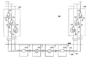
- FIG. 1 is a diagram showing a configuration of a power transmission system according to a first embodiment of the present invention.
- FIG. 2 is a diagram showing an example of a configuration of an underground cable used in the power transmission system according to the first embodiment of the present invention.
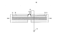
- FIG. 3 is a diagram showing an example of a method of connecting an underground cable in a normal connection portion used in the power transmission system according to the first embodiment of the present invention.
- FIG. 4 is a diagram showing an example of a method of connecting an underground cable in an insulating connection portion used in the power transmission system according to the first embodiment of the present invention.
- FIG. 5 is a figure which shows the other example of the connection method of the underground cable in the insulation connection part used for the power transmission system which concerns on the 1st Embodiment of this invention.
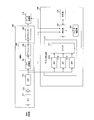
- FIG. 6 is a diagram showing a configuration of the communication system according to the first exemplary embodiment of the present invention.
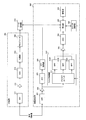
- FIG. 7 is a figure which shows an example of a structure of the communication apparatus in the communication system which concerns on the 1st Embodiment of this invention.
- FIG. 8 is a diagram showing a configuration of CT in the communication apparatus according to the first embodiment of the present invention.
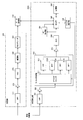
- FIG. 9 is a diagram showing another example of the configuration of the communication device in the communication system according to the first embodiment of the present invention.
- FIG. 10 is a figure which shows the structure of the metal foil electrode in the communication apparatus which concerns on the 1st Embodiment of this invention.
- FIG. 10 is a figure which shows the structure of the metal foil electrode in the communication apparatus which concerns on the 1st Embodiment of this invention.
- FIG. 11 is a figure which shows the structure of the communication part in the communication apparatus which concerns on the 1st Embodiment of this invention.
- FIG. 12 is a figure which shows the structure of the discharge detection part in the communication apparatus which concerns on the 1st Embodiment of this invention.
- FIG. 13 is a diagram showing an example of a BPF impulse response waveform in the discharge detection unit according to the first embodiment of the present invention.
- FIG. 14 is a figure which shows the calculation result by the discharge detection part in the communication apparatus which concerns on the 1st Embodiment of this invention.
- FIG. 15 is a diagram showing a communication band and a detection band in the communication device according to the first embodiment of the present invention.
- FIG. 16 is a figure which shows the structure of the discharge detection part in the modification 1 of the communication apparatus which concerns on the 1st Embodiment of this invention.
- FIG. 17 is a diagram showing the configuration of the discharge detection unit in the communication device according to the second embodiment of the present invention.
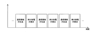
- FIG. 18 is a diagram showing operation timings of the reception unit and the discharge detection unit in the communication device according to the second embodiment of the present invention.
- the present disclosure has been made to solve the above problems, and an object thereof is to provide a communication device capable of transmitting a detection result of partial discharge in an underground cable with a simple configuration.
- the detection result of partial discharge in an underground cable can be transmitted with a simple configuration.
- a communication device is a communication device used in an electric power system including an underground cable, and includes a communication section that outputs a communication signal including communication information, and the communication section that outputs the communication signal.
- a communication signal is output to the shield layer of the underground cable as a communication induced current by inductive coupling, and a change in the current flowing through the shield layer or a change in the potential of the shield layer is acquired as a detected inductive signal by inductive coupling.
- An inductive coupling section for outputting and a discharge detecting section for detecting partial discharge in the underground cable based on the detected inductive signal received from the inductive coupling section are provided.
- the communication signal is output to the shielding layer as a communication induced current by inductive coupling, and the change in the current flowing through the shielding layer or the change in the potential of the shielding layer is acquired as a detected inductive signal by inductive coupling and acquired.
- the detection result of the partial discharge can be transmitted as communication information through the shielding layer of the underground cable.
- the detection result of the partial discharge in the underground cable can be transmitted with a simple configuration.
- the band of the communication induction current and the band of the detection induction signal are different.
- the communication unit can transmit the communication information and the discharge detection unit can detect the partial discharge in parallel, and it is necessary to adjust the relationship between the timing of performing the communication process and the timing of performing the detection process. Therefore, the communication process and the detection process can be simplified.
- the communication unit and the discharge detection unit perform transmission of the communication information and detection of the partial discharge in a time division manner.
- the filter circuit and the analog/digital conversion circuit in the unit can be shared.
- a plurality of the underground cables are connected in the power system, and the inductive coupling section is inductively coupled to the shielding layer at the connection section of the underground cable.
- the portion of the underground cable is detected by the configuration in which the detection guiding signal is detected at the connecting portion of the underground cable and the partial discharge is detected based on the detected guiding signal.
- the discharge can be detected more accurately.
- FIG. 1 is a diagram showing a configuration of a power transmission system according to a first embodiment of the present invention.
- power transmission system 502 includes underground cables 10A, 10B, 10C, ordinary connecting portions 41A, 41B, insulating connecting portions 42A, 42B, and ground connecting portions 43A, 43B.
- each of the underground cables 10A, 10B, and 10C is also referred to as an underground cable 10
- each of the ordinary connecting portions 41A and 41B is also referred to as an ordinary connecting portion 41
- each of the insulating connecting portions 42A and 42B is also referred to as an insulating connecting portion 42.
- the power transmission system 502 includes, for example, an underground part of an electric power system. In other words, a part of the power transmission system 502 is provided, for example, in an underground part of the power system.
- the ground connection unit 43 includes cable terminals 11A, 11B, 11C.
- the underground cable 10 is connected to the cable terminals 11A, 11B, 11C at the ground connection portion 43. More specifically, the underground cable 10A is connected to the cable terminal 11A, the underground cable 10B is connected to the cable terminal 11B, and the underground cable 10C is connected to the cable terminal 11C.
- the ground connection unit 43 is installed, for example, in a substation where the underground cable 10 appears on the ground.
- the ordinary connecting portion 41 and the insulating connecting portion 42 are provided inside the manhole 31.
- FIG. 2 is a diagram showing an example of a configuration of an underground cable used in the power transmission system according to the first embodiment of the present invention.
- the underground cable 10 includes a conductor 71, an inner semiconductive layer 72 made of semiconductive ethylene propylene (EP) rubber, and an insulator 73 made of EP rubber in order from the center. , An outer semiconductive layer 74 which is a semiconductive tape, a conductive shield layer 75, and a vinyl sheath 76.
- EP semiconductive ethylene propylene
- the conductor 71 in the underground cable 10 is used for power transmission and is applied with a high voltage.
- the shielding layer 75 is electrically conductive and is grounded in the middle of the underground cable 10. Therefore, the voltage of the shield layer 75 is lower than that of the conductor 71.
- a three-phase three-wire system is used as a power distribution method.
- underground cables 10A, 10B, and 10C are provided as the three-phase underground cables 10.
- the shielding layers 75 of the underground cables 10A, 10B and 10C are exposed. Terminals are provided on exposed portions of these shielding layers 75, respectively.
- Underground cables 10A, 10B, 10C are connected to ground node 15 at cable terminals 11A, 11B, 11C, respectively. More specifically, the terminals provided on each of the underground cables 10A, 10B, and 10C are connected to the ground node 15 via a cable or the like, so that the shielding layer 75 of the underground cable 10 is grounded.
- the underground cable 10 is composed of a plurality of cables whose ends are connected to each other at the normal connecting portion 41 and the insulating connecting portion 42.
- FIG. 3 is a diagram showing an example of a method of connecting an underground cable in an ordinary connection unit used in the power transmission system according to the first embodiment of the present invention.
- the conductor 71 and the shield layer 75 of the underground cable 10A are mainly shown.
- the contents described below are the same for the underground cable 10B and the underground cable 10C.
- the underground cables 10A1 and 10A2 are connected at the normal connection portion 41.
- the shield layer 75 of the underground cables 10A1 and 10A2 is exposed at the connection portion between the conductors 71 of the underground cables 10A1 and 10A2.
- the shield layer 75 of the underground cable 10A1 and the shield layer 75 of the underground cable 10A2 are connected using, for example, a conductive wire 12.
- the terminal 81 is provided on the exposed portion of the shield layer 75 of the underground cable 10A2.
- the terminal 81 may be provided on an exposed portion of the shield layer 75 of the underground cable 10A1.
- the terminal 81 is connected to the ground node 13 via a cable or the like, so that the shield layer 75 of the underground cable 10A is grounded.
- FIG. 4 is a diagram showing an example of a method of connecting an underground cable in an insulating connection portion used in the power transmission system according to the first embodiment of the present invention.
- the conductor 71 and the shielding layer 75 in the configuration of the underground cable 10A are mainly shown.
- the contents described below are the same for the underground cable 10B and the underground cable 10C.
- the underground cables 10A1 and 10A2 are connected at the insulation connection portion 42.
- the shield layer 75 of the underground cables 10A1 and 10A2 is exposed at the connection portion between the conductors 71 of the underground cables 10A1 and 10A2, and the terminals 81 and the like are provided at the exposed portions.
- the conductor 71 of the underground cable 10A1 and the conductor 71 of the underground cable 10A2 are connected, for example, the terminal 81 in the underground cable 10A1 and the terminal 81 in the underground cable 10A2 are connected using the wire 12.
- the shield layer 75 of the underground cable 10A1 and the shield layer 75 of the underground cable 10A2 are connected.
- FIG. 5 is a diagram showing another example of a method of connecting an underground cable in an insulating connection portion used in the power transmission system according to the first embodiment of the present invention.
- the underground cables 10A1 and 10A2 are connected, the underground cables 10B1 and 10B2 are connected, and the underground cables 10C1 and 10C2 are connected.
- the shield layer 75 of the underground cables 10A1 and 10A2 is exposed at the connection portion between the conductors 71 of the underground cables 10A1 and 10A2, and the connection portion of the conductors 71 of the underground cables 10B1 and 10B2 is connected.
- the shielding layer 75 of the underground cables 10B1 and 10B2 is exposed, and the shielding layer 75 of the underground cables 10C1 and 10C2 is exposed at the connection portion between the conductors 71 of the underground cables 10C1 and 10C2, and the terminals 81 and the like are exposed at the exposed portions. It is provided.
- the shielding layer 75 of the underground cable 10A1 and the shield of the underground cable 10B2 are shielded.
- the layer 75 is connected, and by connecting the terminal 81 in the underground cable 10B1 and the terminal 81 in the underground cable 10C2 using the wire 12, the shielding layer 75 of the underground cable 10B1 and the shielding layer 75 of the underground cable 10C2 are connected.
- the terminal 81 in the underground cable 10C1 and the terminal 81 in the underground cable 10A2 are connected using the wire 12, so that the shielding layer 75 of the underground cable 10C1 and the shielding layer 75 of the underground cable 10A2 are Connected.
- the underground cable 10 may be cross-bonded at the insulating connection portion 42.
- the communication device solves the above problems by the following configurations and operations.
- FIG. 6 is a diagram showing a configuration of the communication system according to the first exemplary embodiment of the present invention.
- the underground cable 10 ⁇ /b>A of the underground cables 10 is mainly shown for ease of explanation.
- the contents described below are the same for the underground cable 10B and the underground cable 10C.
- the communication system 501 includes communication devices 500A, 500B, 500C.
- the communication devices 500A, 500B, 500C are used in a power system including the underground cable 10.
- each of the communication devices 500A, 500B and 500C is also referred to as a communication device 500.
- the communication device 500 is provided corresponding to, for example, the insulation connection part 42 or the ground connection part 43.
- the communication device 500A is provided corresponding to the insulating connection portion 42A
- the communication device 500B is provided corresponding to the insulating connection portion 42B
- the communication device 500C is connected to the ground. It is provided corresponding to the portion 43.
- the communication device 500 exchanges communication information with each other via the underground cable 10 by inductive coupling with the shield layer 75 in the underground cable 10A.
- the communication devices 500A and 500B detect partial discharge of the underground cable 10.
- the communication devices 500A and 500B generate a communication signal including the detection result of the partial discharge of the underground cable 10 as communication information, and transmit the generated communication signal to another communication device 500 such as the communication device 500C.
- the communication devices 500A and 500B generate, for example, a communication signal including various measurement results obtained by the one or more sensors 14 as communication information, and transmit the generated communication signal to another communication device 500 such as the communication device 500C. To do.
- the communication device 500 can perform communication up to a distance of several km at a variable transmission rate of 20 kbps to 130 kbps by using a low frequency PLC (Power Line Communication) used for communication of a smart meter or the like. Further, the communication device 500 can also perform shorter distance communication at a maximum transmission rate of 200 Mbps by using the high frequency PLC.
- PLC Power Line Communication
- a power coil is attached to the underground cable 10A.
- An induced current due to a current flowing through the conductor 71 of the underground cable 10 flows through the power supply coil.
- the power supply coil can take out the current.
- the communication device 500 operates by, for example, the electric power obtained by the power supply coil.
- FIG. 7 is a figure which shows an example of a structure of the communication apparatus in the communication system which concerns on the 1st Embodiment of this invention.
- communication device 500 includes electromagnetic coupling unit 120, communication unit 200, and discharge detection unit 300.
- the electromagnetic coupling part 120 is inductively coupled to the shield layer 75 of the underground cable 10. Specifically, the electromagnetic coupling part 120 electromagnetically couples with the shield layer 75 of the underground cable 10.
- the electromagnetic coupling part 120 is an example of an inductive coupling part.
- the communication unit 200 transmits communication information via the shielding layer 75.
- the discharge detector 300 detects a partial discharge in the underground cable 10.
- the electromagnetic coupling unit 120 includes a current transformer (CT) 100 and a signal distributor 110A.
- CT current transformer
- the electromagnetic coupling part 120 is electromagnetically coupled to the shielding layer 75 in the insulating connection part 42 which is a connection part of the underground cable 10, for example.
- FIG. 8 is a diagram showing a configuration of CT in the communication device according to the first embodiment of the present invention.
- CT 100 includes ring core 101 and winding 102.
- a winding 102 is wound around the ring core 101.
- the winding 102 is connected to the signal distributor 110A.
- the CT 100 is attached, for example, so that the conductive cable 53 penetrates the ring core 101.
- the conductive cable 53 is, for example, the wire 12.
- CT 100 of communication devices 500A and 500B in insulating connection portion 42 connects shield layer 75 of underground cable 10A1 and shield layer 75 of underground cable 10A2.
- the wire 12 is attached so as to penetrate the ring core 101.
- CT 100 of the communication device 500C in the ground connection unit 43 is attached such that the cable connecting between the cable terminal 11A and the ground node 15 penetrates the ring core 101.
- a current according to the communication signal transmitted from the communication unit 200 flows through the winding 102.
- an inductive current flows through the conductive cable 53 and the shielding layer 75 due to inductive coupling.
- the induced current flowing through the shield layer 75 will also be referred to as a communication induced current.
- the electromagnetic coupling unit 120 functions as a current detection unit that detects a current flowing through the shielding layer 75. More specifically, when an electric current flows through the shield layer 75 and the conductive cable 53, an inductive current flows through the winding 102 due to inductive coupling. The electromagnetic coupling unit 120 detects the induced current flowing through the winding 102.
- the communication unit 200 and the discharge detection unit 300 receive, via the signal distributor 110A, a detection induction signal which is a signal corresponding to a change in the induction current flowing through the winding 102.
- the electromagnetic coupling unit 120 receives a communication signal from the communication unit 200, and outputs the received communication signal to the shielding layer 75 of the underground cable 10 as a communication induction current by electromagnetic coupling. Further, the electromagnetic coupling unit 120 acquires a change in current flowing through the shielding layer 75 as a detection guidance signal by electromagnetic coupling, and outputs an analog signal corresponding to the acquired detection guidance signal to the discharge detection unit 300.
- FIG. 9 is a diagram showing another example of the configuration of the communication device in the communication system according to the first embodiment of the present invention.
- communication device 500 includes electrostatic coupling section 121, communication section 200, and discharge detection section 300.
- the electrostatic coupling part 121 is inductively coupled to the shield layer 75 of the underground cable 10. Specifically, the electrostatic coupling part 121 electrostatically couples with the shielding layer 75 of the underground cable 10.
- the electrostatic coupling part 121 is an example of an inductive coupling part.
- the electrostatic coupling part 121 includes metal foil electrodes 105A and 105B and a signal distributor 110B.
- the electrostatic coupling part 121 electrostatically couples with the shielding layer 75 in the insulating connection part 42 which is a connection part of the underground cable 10, for example.
- FIG. 10 is a diagram showing a configuration of a metal foil electrode in the communication device according to the first embodiment of the present invention.
- metal foil electrodes 105A and 105B are connected to signal distributor 110B.
- the metal foil electrodes 105A and 105B are, for example, attached to the surface of the sheath 76 of the underground cable 10 on opposite sides to each other via the insulating cylinder 77 in the insulating connection portion 42. More specifically, for example, in the insulated connection portion 42 to which the underground cables 10A1 and 10A2 are connected, the metal foil electrode 105A is attached to the surface of the sheath 76 of the underground cable 10A1, and the metal foil electrode 105B is connected to the underground. It is attached to the surface of the sheath 76 of the cable 10A2.
- the metal anchor electrodes 105A and 105B may be attached so as to cover the outer circumference of the sheath 76 of the underground cable 10A2. Further, the position and the number of the metal anchor electrodes 105A and 105B to be attached are not limited, and three or more metal anchor electrodes may be attached.
- a current corresponding to the communication signal transmitted from the communication unit 200 flows to the metal foil electrodes 105A and 105B.
- a communication induction current flows through the conductive cable 53 and the shielding layer 75 due to electrostatic coupling.
- the electrostatic coupling unit 121 functions as a current detection unit that detects a current flowing through the shielding layer 75. More specifically, when a current flows through the shield layer 75 and the conductive cable 53, an induced current flows through the metal foil electrodes 105A and 105B due to inductive coupling. The electrostatic coupling part 121 detects the induced current flowing to the metal foil electrodes 105A and 105B.
- the communication unit 200 and the discharge detection unit 300 receive a detection induction signal which is a signal corresponding to a change in the potential of the shielding layer 75 via the signal distributor 110B.
- the electrostatic coupling unit 121 receives a communication signal from the communication unit 200, and outputs the received communication signal to the shielding layer 75 of the underground cable 10 as a communication induction current by electrostatic coupling. Further, the electrostatic coupling unit 121 acquires a change in the potential of the shielding layer 75 as a detection guidance signal by electrostatic coupling, and outputs an analog signal corresponding to the acquired detection guidance signal to the discharge detection unit 300.
- the signal distributor 110A in the electromagnetic coupling unit 120 and the signal distributor 110B in the electrostatic coupling unit 121 are also simply referred to as the signal distributor 110.
- the communication unit 200 acquires communication information from an analog signal received via the signal distributor 110, that is, a communication signal from another communication device 500.
- the communication unit 200 of the communication device 500C in the ground connection unit 43 transmits the acquired communication information to the central monitoring device 103 using wireless communication such as a mobile phone.
- the discharge detection unit 300 detects partial discharge in the underground cable 10 based on the analog signal received via the signal distributor 110.
- the discharge detection unit 300 outputs detection information indicating the detection result of partial discharge to the communication unit 200.
- the communication unit 200 transmits communication information using a communication induced current that is an induced current flowing through the shielding layer 75 due to the inductive coupling of the inductive coupling unit. More specifically, the communication unit 200 communicates with the communication unit 200 in another communication device 500 using the communication induced current.
- FIG. 11 is a diagram showing a configuration of a communication unit in the communication device according to the first embodiment of the present invention.
- communication unit 200 includes a data processing unit 210, a transmission unit 220, and a reception unit 260.
- the receiving unit 260 converts the communication signal received via the signal distributor 110 into a digital signal, generates demodulated data by performing demodulation processing and decoding processing on the converted digital signal, and generates the demodulated data.
- the data is output to the data processing unit 210.
- the data processing unit 210 Upon receiving the demodulated data from the reception unit 260, the data processing unit 210 acquires communication information from the received demodulated data.
- the data processing unit 210 Upon receiving the detection information from the discharge detection unit 300, the data processing unit 210 generates communication data that includes the received detection information as communication information, and outputs the generated communication data to the transmission unit 220. Further, when receiving the measurement information indicating the measurement result from the sensor 14, the data processing unit 210 generates communication data including the received measurement information as communication information, and outputs the generated communication data to the transmission unit 220.
- the communication unit 200 outputs a communication signal including communication information. More specifically, the transmission unit 220 in the communication unit 200 generates a communication signal by performing an encoding process and a modulation process on the communication data received from the data processing unit 210, and the generated communication signal is a signal distributor. Output to 110.
- the data processing unit 210 generates communication data including information indicating the ID of its own communication device 500 (hereinafter, also referred to as ID information) as a part of the communication information.
- ID information information indicating the ID of its own communication device 500
- the data processing unit 210 outputs the generated communication data to the transmission unit 220.
- the data processing unit 210 confirms the ID information included in the demodulated data received from the receiving unit 260, and when the confirmed ID information indicates the ID of the communication device 500 of its own, the data processing unit 210 extracts the communication information from the demodulated data. get.
- the transmission unit 220 includes an FEC (Forward Error Correction) encoder 230 that performs coding processing in forward error correction, a modulation unit 240 that performs modulation processing, a DAC (Digital Analog Converter) 251, and a bandpass filter (BPF) 252. , And a transmission amplifier 253.
- the FEC encoder 230 has a scrambler 231, an encoder 232, and an interleaver 233.
- the modulator 240 includes a mapper 241 and an IFFT (Inverse Fast Fourier Transform) processor 242.
- the scrambler 231 scrambles the communication data received from the data processing unit 210, and outputs the processed communication data to the RS encoder 232.
- the encoder 232 performs an encoding process on the communication data received from the scrambler 231, and outputs the processed communication data to the interleaver 233.
- the interleaver 233 performs iterative encoding processing and interleaving processing on the communication data received from the encoder 232, and outputs the processed communication data to the mapper 241.
- the mapper 241 generates modulated data by modulating the communication data received from the interleaver 233 according to, for example, the DBPSK method (Differential Binary Phase Shift Keying), and outputs the generated modulated data to the IFFT processing unit 242.
- DBPSK method Different Binary Phase Shift Keying
- the mapper 241 may be configured to generate modulated data by modulating the communication data received from the interleaver 233 according to the DQPSK method (Differential Quaternary Phase Shift Keying), or according to the D8PSK method (Differential Octal Phase Shift Keying). It may be configured to generate modulated data.
- the IFFT processing unit 242 outputs, to the DAC 251, the modulated data obtained by performing signal processing such as IFFT in the orthogonal frequency division multiplexing method (OFDM: Orthogonal Frequency Division Multiplexing) on the modulated data received from the mapper 241.
- OFDM Orthogonal Frequency Division Multiplexing
- the DAC 251 converts the modulation data received from the IFFT processing unit 242 into an analog signal and outputs it to the BPF 252.
- the BPF 252 outputs, to the transmission amplifier 253, an analog signal obtained by attenuating the frequency component of the analog signal received from the DAC 251 outside the predetermined frequency band.
- the transmission amplifier 253 amplifies the analog signal received from the BPF 252 with a predetermined gain, and outputs the amplified analog signal to the signal distributor 110 as a communication signal.
- the reception unit 260 includes a high-pass filter (HPF) 271, a reception amplifier 272, an ADC (Analog Digital Converter) 273, a demodulation unit 280 that performs demodulation processing, and an FEC decoder 290 that performs decoding processing in forward error correction. ..
- the demodulation unit 280 includes an FFT (Fast Fourier Transform) processing unit 281 and a demodulator 282.
- the FEC decoder 290 has a deinterleaver 291, a decoder 292, and a descrambler 293.
- the HPF 271 outputs, to the reception amplifier 272, a communication signal obtained by attenuating a frequency component of a predetermined frequency or less among the frequency components of the communication signal received via the signal distributor 110.
- the receiving amplifier 272 amplifies the communication signal received from the HPF 271 with a predetermined gain and outputs the amplified communication signal to the ADC 273.
- the ADC 273 converts a communication signal, which is an analog signal received from the reception amplifier 272, into a digital signal and outputs the digital signal to the FFT processing unit 281.
- the FFT processing unit 281 performs signal processing such as FFT in the OFDM system on the digital signal received from the ADC 273, and outputs the processed digital signal to the demodulator 282.
- the demodulator 282 generates demodulated data obtained by demodulating the digital signal received from the FFT processing unit 281 according to, for example, the DBPSK method, and outputs the generated demodulated data to the deinterleaver 291.
- the deinterleaver 291 performs iterative decoding processing and deinterleave processing on the demodulated data received from the demodulator 282, and outputs the processed demodulated data to the decoder 292.
- the decoder 292 decodes the demodulated data received from the deinterleaver 291, and outputs the processed demodulated data to the descrambler 293.
- the descrambler 293 performs scramble decoding processing on the demodulated data received from the decoder 292, and outputs the processed demodulated data to the data processing unit 210.
- Discharge detection unit 300 detects partial discharge in underground cable 10 based on the detection induction signal received from electromagnetic coupling unit 120 or electrostatic coupling unit 121.
- FIG. 12 is a diagram showing the configuration of the discharge detection unit in the communication device according to the first embodiment of the present invention.
- the receiving unit 260 in the communication unit 200 is shown in addition to the discharge detecting unit 300.
- the discharge detection unit 300 includes an HPF 301, an LNA (Low Noise Amplifier) 302, an ADC 303, an FFT processing unit 304, a filter processing unit 310, an AGC (Automatic Gain Control) amplifier 305, and It includes an ADC 306, a detection unit 320, a switch control unit 330, and a storage unit 340.
- LNA Low Noise Amplifier
- ADC Analog to Digital Converter
- the filter processing unit 310 has an analog switch 311 and BPFs 312A, 312B and 312C.
- each of the BPFs 312A, 312B, and 312C will also be referred to as a BPF 312.
- the HPF 301 outputs to the LNA 302 a signal obtained by attenuating a frequency component of a predetermined frequency or lower among the frequency components of the analog signal received via the signal distributor 110.
- the analog signal received via the signal distributor 110 contains a lot of noise in a band of, for example, less than 1.6 MHz, which is superimposed on the transmission path of the underground cable 10 or the like.
- the HPF 301 removes noise included in the analog signal received via the signal distributor 110 by attenuating frequency components of less than 1.6 MHz, for example.
- the LNA 302 amplifies the analog signal received from the HPF 301 with a predetermined gain and outputs the amplified analog signal to the ADC 303 and the filter processing unit 310.
- the ADC 303 converts the analog signal received from the LNA 302 into a digital signal and outputs the digital signal to the FFT processing unit 304.
- the FFT processing unit 304 performs signal processing such as FFT on the digital signal received from the ADC 303, and outputs the processed digital signal to the detection unit 320.
- the detection unit 320 generates a frequency spectrum of the analog signal output from the HPF 301 based on the digital signal received from the FFT processing unit 304, and outputs the generated frequency spectrum to the switch control unit 330.
- the switch control unit 330 switches the analog switch 311 by generating a switch control signal based on the frequency spectrum received from the detection unit 320 and outputting the generated switch control signal to the analog switch 311.
- the analog switch 311 switches the output destination BPF 312 of the analog signal received from the LNA 302 according to the switch control signal received from the switch control unit 330.
- the passbands of the three BPFs 312 are different.
- the pass band of BPF312A is 5 MHz or more and less than 10 MHz
- the pass band of BPF312B is 10 MHz or more and less than 15 MHz
- the pass band of BPF312C is 15 MHz or more and less than 20 MHz.
- the switch control unit 330 selects one BPF 312 to be the output destination of the analog signal by the analog switch 311 from the three BPFs 312. More specifically, the switch control unit 330 determines the pass band having the smallest noise component in the analog signal output from the LNA 302 among the pass bands of the three BPFs 312, and selects the BPF 312 corresponding to the pass band. To do.
- the switch control unit 330 selects any one BPF 312 from the plurality of BPFs 312 based on the current detected by the electromagnetic coupling unit 120 or the electrostatic coupling unit 121. More specifically, based on the frequency spectrum received from the detection unit 320, the switch control unit 330 sets the pass band in which the analog signal output from the LNA 302 is the lowest among the pass bands of the three BPFs 312. Select the corresponding BPF 312.
- the current waveform due to partial discharge is an impulse waveform. Since the components of the impulse waveform in the frequency spectrum spread equally in the pass bands of each BPF 312, the difference in the spectrum level in each pass band caused by the components of the impulse waveform is so small that it can be ignored. Therefore, based on the frequency spectrum, of the pass bands of the three BPFs 312, the pass band in which the analog signal output from the LNA 302 has the lowest signal level can be regarded as the pass band in which the noise component is the smallest.
- the switch control unit 330 outputs the switch control signal to the analog switch 311 to switch the output destination of the analog signal by the analog switch 311 to the selected BPF 312.
- the switch control unit 330 selects the BPF 312 based on the frequency spectrum received from the detection unit 320 on a regular or irregular basis, and switches the analog switch 311 according to the selection result.
- the switch control unit 330 is not limited to the configuration in which the analog switch 311 is switched based on the frequency spectrum received from the detection unit 320, and regularly or irregularly monitors the digital signal received by the detection unit 320 from the ADC 306 to obtain a digital signal.
- the analog switch 311 may be switched based on the change in the value of, that is, the amount of the noise component included in the digital signal.
- the BPF 312 receives an analog signal according to an induced current flowing through the winding 102, which is an example of a signal based on a current detected by the electromagnetic coupling section 120 or the electrostatic coupling section 121. More specifically, the BPF 312 receives the analog signal via the HPF 301, the LNA 302 and the analog switch 311. The BPF 312 outputs, to the AGC amplifier 305, an analog signal obtained by attenuating the frequency component of the analog signal received from the analog switch 311 outside the pass band of itself.
- the AGC amplifier 305 amplifies the signal received from the BPF 312 and outputs it to the ADC 306 so that the output level of the analog signal to the ADC 306 becomes constant.
- the ADC 306 converts the analog signal received from the AGC amplifier 305 into a digital signal and outputs the digital signal to the detection unit 320.
- the detection unit 320 detects a partial discharge in the underground cable 10 based on the output of at least one BPF 312 of the three BPFs 312 and the characteristic data regarding the physical properties of the corresponding BPF 312. More specifically, the detection unit 320 detects the partial discharge in the underground cable 10 based on the output of the BPF 312 selected by the switch control unit 330 and the characteristic data regarding the physical properties of the BPF 312.
- the detection unit 320 receives from the ADC 306 a digital signal S obtained by amplifying and digitally converting the analog signal output by the selected BPF 312, and performs an operation using the received digital signal S and the characteristic data of the BPF 312. , Partial discharge in the underground cable 10 is detected.
- the storage unit 340 stores characteristic data regarding the characteristics of the three BPFs 312, respectively. More specifically, the storage unit 340 stores, as the characteristic data, the pulse response characteristics of the three BPFs 312, for example, the impulse response waveform Imp.
- the switch control unit 330 outputs selection information indicating the selected BPF 312 to the detection unit 320.
- the detection unit 320 acquires the impulse response waveform Imp of the BPF 312 indicated by the selection information received from the switch control unit 330 from the storage unit 340, and performs an operation using the acquired impulse response waveform Imp and the digital signal S received from the ADC 306. By doing so, the partial discharge in the underground cable 10 is detected.
- a part or all of the FFT processing unit 304, the detection unit 320, and the switch control unit 330 are realized by operating a processor such as a CPU (Central Processing Unit) and a DSP (Digital Signal Processor) with software. Further, some or all of the functions of the FFT processing unit 304, the detection unit 320, and the switch control unit 330 are realized by operating a processor such as a CPU and a DSP with software, for example.
- a processor such as a CPU (Central Processing Unit) and a DSP (Digital Signal Processor) with software.
- FIG. 13 is a diagram showing an example of a BPF impulse response waveform in the discharge detection unit according to the first embodiment of the present invention.
- the impulse response waveform Imp of the BPF 312 is stored in the storage unit 340 as a digital signal whose sample number is K in the period T1 from time t0 to time ta.
- the impulse response waveform Imp is a waveform having one or more maximum values and one or more minimum values.
- the detection unit 320 calculates the Xth value of the K sampling values included in the digital signal S in the period T1 from the time t to the time t+T1 and the Xth value of the impulse response waveform Imp according to the following equation (1). Of the sampling value and the K values obtained by the multiplication for each sampling value are added to calculate the operation value Y(t).
- S(t) is the value of the digital signal S at time t.
- FIG. 14 is a diagram showing a calculation result by the discharge detection unit in the communication device according to the first embodiment of the present invention.
- the vertical axis represents voltage and the horizontal axis represents time.
- the detection unit 320 calculates the calculation value Y(t) corresponding to each start time by shifting the start time of the period T1 by one sample of the digital signal S.
- the detection unit 320 may calculate the calculated value Y(t) by multiplying the digital signal S by the impulse response waveform Imp every time the digital signal S for one sample is received from the ADC 306, or may be received from the ADC 306.
- the calculated value Y(t) may be calculated by accumulating a predetermined number, for example, K sampling values of the digital signal S, and multiplying each accumulated sampling value by the impulse response waveform Imp.
- the calculated value Y(tk) becomes a value close to zero.
- the digital signal S in the period T1 from the time tm to the time tm+T1 includes an impulse waveform, the calculated value Y(tm) becomes a relatively large value.
- the detection unit 320 detects partial discharge based on the calculated calculation value Y(t). For example, the storage unit 340 stores the threshold value ThA of the calculated value Y(t) used for detecting partial discharge. The detection unit 320 compares the calculated value Y(t) with the threshold value ThA, and when the calculated value Y(t) is greater than or equal to the threshold value ThA, determines that partial discharge has occurred.
- the detection unit 320 when detecting a partial discharge, the detection unit 320 generates detection information indicating the detection result of the partial discharge, and outputs the generated detection information to the data processing unit 210.
- the detection unit 320 calculates the level of the impulse signal due to the partial discharge. More specifically, for example, the storage unit 340 stores the gain of the LNA 302 and the input/output ratio of the impulse response characteristic of the BPF 312. When the gain of the AGC amplifier 305 can be monitored, the detection unit 320 acquires the gain of the LNA 302 and the input/output ratio of the impulse response characteristics of the selected BPF 312 from the storage unit 340, and the gain of the LNA 302, the gain of the AGC amplifier 305, The level of the impulse signal due to the partial discharge is calculated based on the input/output ratio of the impulse response characteristic of the selected BPF 312 and the calculated value Y(t).
- the detection unit 320 calculates the phase of the impulse signal due to partial discharge (hereinafter, also referred to as impulse phase) at the high voltage applied to the conductor 71 of the underground cable 10. More specifically, the data processing unit 210 detects the waveform of 50 Hz or 60 Hz of the induced current due to the current flowing through the conductor 71, for example, via the above-described power supply coil attached to the underground cable 10. The data processing unit 210 detects the zero-cross point of the waveform of the high voltage applied to the conductor 71 based on the detected waveform.
- the data processing unit 210 generates zero-cross information indicating the timing of the detected zero-cross point and outputs it to the detection unit 320.
- the detection unit 320 calculates the impulse phase based on the received zero-cross information and the timing of generating the impulse signal due to the partial discharge.
- the data processing unit 210 in the communication device 500 is configured to receive information regarding the high voltage applied to the conductor 71, for example, the zero-cross information, from the central monitoring device 103 via the communication device 500C in the ground connection unit 43. May be.
- the detection unit 320 creates partial discharge information including the level of the impulse signal and the impulse phase due to the detected partial discharge, and saves the created partial discharge information in the storage unit 340.
- the detection unit 320 updates the threshold ThA based on the partial discharge information stored in the storage unit 340 using, for example, a machine learning method.
- FIG. 15 is a diagram showing a communication band and a detection band in the communication device according to the first embodiment of the present invention.
- the band of the communication induction current used by communication unit 200 for transmitting communication information is different from the band of the detection induction signal used by discharge detection unit 300 for detecting partial discharge.
- the band of the communication induced current (hereinafter, also referred to as the communication band) used by the communication unit 200 for transmitting the communication information is, for example, 10 kHz or more and 450 kHz or less, and the discharge detection unit 300 detects the partial discharge.
- the band of the detection induction signal used for (hereinafter, also referred to as a detection band) is, for example, 1.6 MHz or more and 50 MHz or less.
- the BPF 252 in the transmission unit 220 and the HPF 271 in the reception unit 260 have a pass band of 10 kHz or more and attenuate components with a frequency of less than 10 kHz, while the HPF 301 of the discharge detection unit 300 has a pass band of 1.
- a frequency component of 6 MHz or more and less than 1.6 MHz is attenuated.
- the communication unit 200 and the discharge detection unit 300 perform transmission of communication information and detection of partial discharge in parallel.
- FIG. 16 is a figure which shows the structure of the discharge detection part in the modification 1 of the communication apparatus which concerns on the 1st Embodiment of this invention.
- the reception unit 260 in the communication unit 200 is shown.
- discharge detecting section 300A does not include ADC 303 and filter processing section 310 has LPF 313 as compared with discharge detecting section 300 shown in FIG. More specifically, the discharge detection unit 300A includes an HPF 301, an LNA 302, an FFT processing unit 304, a filter processing unit 310, an AGC amplifier 305, an ADC 306, a detection unit 320, a switch control unit 330, and a storage unit. 340 and. Except for the contents described below, the discharge detector 300 is the same as the discharge detector 300 shown in FIG.
- the filter processing unit 310 includes an analog switch 311, BPFs 312A, 312B and 312C, and a low pass filter (LPF) 313.
- the cutoff frequency of the LPF 313 is, for example, a frequency that is 1 ⁇ 2 or less of the sampling frequency of the ADC 306.
- the switch control unit 330 periodically or irregularly selects the LPF 313 as a filter to be the output destination of the analog signal by the analog switch 311, and switches the output destination of the analog signal by the analog switch 311 to the LPF 313.
- the LPF 313 outputs to the AGC amplifier 305 an analog signal obtained by attenuating a frequency component of a predetermined frequency or higher among the frequency components of the analog signal received from the analog switch 311.
- the AGC amplifier 305 amplifies the signal received from the LPF 313 and outputs it to the ADC 306 so that the output level of the analog signal to the ADC 306 becomes constant.
- the ADC 306 converts the analog signal received from the AGC amplifier 305 into a digital signal and outputs the digital signal to the FFT processing unit 304.
- the FFT processing unit 304 performs signal processing such as FFT on the digital signal received from the ADC 306, and outputs the processed digital signal to the detection unit 320.
- the detection unit 320 generates a frequency spectrum of the analog signal output by the LPF 313 based on the digital signal received from the FFT processing unit 304, and outputs the generated frequency spectrum to the switch control unit 330.
- the switch control unit 330 selects one BPF 312 to be the output destination of the analog signal by the analog switch 311 from the three BPFs 312 based on the frequency spectrum received from the detection unit 320.
- the switch control unit 330 outputs the switch control signal to the analog switch 311 to switch the output destination of the analog signal by the analog switch 311 to the selected BPF 312.
- the switch control unit 330 outputs selection information indicating that the LPF 313 has been selected to the detection unit 320.
- the communication device 500 may be configured to operate with the electric power obtained by using the CT100.
- the communication device 500 operates by using an induced current of a current flowing through the shield layer 75 of the underground cable 10 and in a frequency band different from the frequency band of the communication signal transmitted and received by the communication device 500. ..
- a sheath current that is an induced current due to the influence of a current for power transmission that flows through the conductor 71 of the underground cable 10. Is flowing.
- the sheath current flowing through the shielding layer 75 of the underground cable 10 can be taken out by providing the CT 100 in the underground cable 10.
- the communication device 500 includes a filter that allows a current having a frequency of 60 Hz or less to pass therethrough.
- the communication device 500 extracts low-frequency current of 50 Hz or 60 Hz from each extracted sheath current by using a filter.
- the communication device 500 generates a power supply current sufficient to operate the communication device 500 by rectifying and combining the extracted low frequency currents.
- the communication device 500 operates with the generated power supply current.
- the detection unit 320 in the discharge detection unit 300 causes the partial discharge in the underground cable based on the output of the BPF 312 and the characteristic data regarding the physical properties of the BPF 312.
- the configuration is such that the detection is performed, the configuration is not limited to this.
- the discharge detection unit 300 may be configured to detect partial discharge by another method.
- discharge detection unit 300 may have the following configuration. That is, the HPF 301 outputs, to the LNA 302, an analog signal obtained by attenuating a frequency component of a predetermined frequency or lower among the frequency components of the analog signal received via the signal distributor 110. LNA 302 amplifies the analog signal received from HPF 301 with a predetermined gain and outputs it to ADC 303.
- the ADC 303 converts the analog signal received from the LNA 302 into a digital signal and outputs the digital signal to the FFT processing unit 304.
- FFT processing section 304 performs signal processing such as FFT on the digital signal received from ADC 303, and outputs the processed digital signal to detection section 320.
- the detection unit 320 generates a frequency spectrum of the analog signal output by the HPF 301 based on the digital signal received from the FFT processing unit 304, and detects partial discharge based on the generated frequency spectrum.
- the filter processing unit 310 in the discharge detection unit 300 is configured to have three BPFs 312, but the configuration is not limited to this.
- the filter processing unit 310 may have a configuration having two or less BPFs 312, or may have a configuration having four or more BPFs 312.
- the communication device according to the first embodiment of the present invention is configured to be provided in the insulation connection part 42 and the ground connection part 43, but the configuration is not limited to this.
- the communication device 500 may be provided in the normal connection unit 41.
- the CT 100 of the communication device 500 in the normal connection portion 41 is attached so that the cable connecting between the terminal 81 provided in the shielding layer 75 and the ground node 13 penetrates the ring core 101.
- the storage unit 340 stores the impulse response waveform Imp as the characteristic data of the BPF 312, and the detection unit 320 uses the digital signal.
- the calculation value Y(t) is calculated by multiplying S by the impulse response waveform Imp in the storage unit 340.
- the calculation value Y(t) is not limited to this. Good. That is, the storage unit 340 stores a sine wave waveform having a frequency included in the pass band of the BPF 312.
- the detection unit 320 calculates the calculated value Y(t) by multiplying the digital signal S by the waveform of the sine wave in the storage unit 340.
- the storage unit 340 stores characteristic data other than the pulse response characteristic as the characteristic data of the BPF 312.
- the detection unit 320 detects the partial discharge based on the digital signal S and the characteristic data in the storage unit 340.
- the communication device is configured to perform communication information transmission and partial discharge detection in parallel, but the configuration is not limited to this.
- the communication unit 200 and the discharge detection unit 300 may be configured to perform transmission of communication information and detection of partial discharge in time division. More specifically, the communication device 500 causes the communication unit 200 to transmit communication information and the discharge detection unit 300 to detect partial discharge in time.
- the data processing unit 210 controls the transmission timing of the communication signal by each communication device 500 and the detection timing of the partial discharge by the detection unit 320. More specifically, for example, the data processing unit 210 in any one communication device 500 in the communication system 501 generates communication data including synchronization information indicating the transmission timing of a communication signal by each communication device 500 as communication information, It transmits to another communication apparatus 500 via the transmission part 220 and the signal distributor 110. Each communication device 500 transmits a communication signal at the timing indicated by the synchronization information.
- the data processing unit 210 generates a synchronization signal indicating the detection timing of partial discharge, and outputs the generated synchronization signal to the detection unit 320.
- the detection unit 320 detects partial discharge at the timing indicated by the synchronization signal. In this way, the data processing unit 210 controls the transmission timing of the communication signal and the detection timing of the partial discharge to be different from each other, so that the communication unit 200 can transmit the communication information and the discharge detection unit 300 can detect the partial discharge. It is time-shared.
- the communication band of the communication unit 200 is 10 kHz or more and 450 kHz or less
- the detection band of the discharge detection unit 300 is 1.6 MHz or more and 50 MHz or less.
- the communication band of the communication unit 200 and the detection band of the discharge detection unit 300 may partially or entirely overlap.
- the communication device 500 causes the communication unit 200 to transmit the communication information and the discharge detection unit 300 to detect the partial discharge alternately in time.
- the communication device 500C in the ground connection unit 43 is configured to include the communication unit 200 and the discharge detection unit 300, but the configuration is not limited to this. ..
- the communication device 500C in the ground connection unit 43 may include the communication unit 200 but not the discharge detection unit 300.
- the electromagnetic coupling part 120 is electromagnetically coupled to the shielding layer 75 at the connection part of the underground cable 10 such as the ground connection part 43 and the insulation connection part 42.
- the electromagnetic coupling part 120 may be configured to be electromagnetically coupled to the shield layer 75 at a portion other than the connection portion of the underground cable 10.
- the data processing unit 210 is configured to generate the communication data including the measurement information received from the sensor 14 as the communication information, but the configuration is not limited to this. Not something to do.
- the data processing unit 210 may generate communication data including the detection information received from the discharge detection unit 300 as communication information, but may not generate communication data including the measurement information received from the sensor 14.
- the data processing unit 210 is configured to generate the communication data including the ID information of the communication device 500 of itself as a part of the communication information. , But is not limited to this.
- the data processing unit 210 may be configured to generate communication data that does not include ID information.
- the discharge detection unit 300 is configured to include the AGC amplifier 305, but the configuration is not limited to this.
- the discharge detection unit 300 may be configured to include a normal amplifier having no automatic gain control function, instead of the AGC amplifier 305.
- the discharge detection unit 300 may be configured to include an amplifier whose gain can be adjusted from the outside, instead of the AGC amplifier 305.
- the detection unit 320 generates a gain control signal according to the maximum value of the digital signal S in a predetermined period, for example, a period of several cycles of the high voltage applied to the conductor 71, and the generated gain control signal. Is output to the amplifier to adjust the gain of the amplifier.
- the switch control unit 330 is one of the three BPFs 312 that should be the output destination of the analog signal by the analog switch 311. It is assumed that the BPF 312 is selected and the detection unit 320 detects the partial discharge by the calculation using the output of the selected BPF 312, that is, the digital signal S received via the ADC 306 and the corresponding impulse response waveform Imp.
- the present invention is not limited to this, and the following configurations may be adopted. That is, the switch control unit 330 selects two or more BPFs 312 to which the analog switch 311 outputs analog signals.
- the detection unit 320 performs an operation using the digital signal S and the corresponding impulse response waveform Imp for each selected BPF 312, and detects partial discharge based on each operation result.
- the communication device is used in a power system including the underground cable 10.
- the communication unit 200 outputs a communication signal including communication information.
- the inductive coupling unit outputs the communication signal from the communication unit 200 as a communication induced current to the shield layer 75 of the underground cable 10 by inductive coupling, and changes the current flowing through the shield layer 75 or the potential of the shield layer 75. Is obtained as a detection induction signal by inductive coupling and is output to the discharge detection unit 300.
- Discharge detection unit 300 detects partial discharge in underground cable 10 based on the detection induction signal received from the inductive coupling unit.
- the communication signal is output to the shield layer 75 as a communication induced current by inductive coupling, and a change in the current flowing through the shield layer 75 or a change in the potential of the shield layer 75 is acquired as a detection inductive signal by inductive coupling.
- the detection result of the partial discharge can be transmitted as communication information through the shielding layer 75 of the underground cable 10.
- the communication device can transmit the detection result of the partial discharge in the underground cable 10 with a simple configuration.
- the communication device is different in the band of the communication induction current and the band of the detection induction signal.
- transmission of communication information by the communication unit 200 and detection of partial discharge by the discharge detection unit 300 can be performed in parallel, and the relationship between the timing of performing communication processing and the timing of performing detection processing is adjusted.
- the communication process and the detection process can be simplified because there is no need to do so.
- a plurality of underground cables 10 are connected in the power system, and the inductive coupling section is inductively coupled to the shielding layer 75 at the connection section of the underground cable 10. ..
- the partial discharge of can be detected more accurately.
- the partial discharge detection device is used in a power system including the underground cable 10.
- the inductive coupling section detects a current flowing through the shield layer 75 of the underground cable 10.
- the discharge detection unit 300 detects partial discharge in the underground cable 10 based on the detected current that is the current detected by the inductive coupling unit.
- Discharge detection unit 300 includes a BPF 312 that receives an analog signal based on the detected current, and a storage unit 340 that stores characteristic data of BPF 312.
- the discharge detection unit 300 detects a partial discharge based on the output of the BPF 312 and the characteristic data in the storage unit 340.
- the partial discharge is detected based on the output of the BPF 312 receiving the analog signal based on the current flowing through the shield layer 75 and the characteristic data of the BPF 312, and thus the waveform of the analog signal corresponding to the characteristic data is generated.
- the presence or absence can be detected.
- the current waveform due to the partial discharge can be detected while reducing the influence of the noise component included in the current flowing through the shielding layer 75.
- the partial discharge detection device can detect the partial discharge in the underground cable 10 more accurately. Further, generally, in order to detect an impulse signal due to partial discharge by digital signal processing, an ADC capable of high-speed sampling at a sampling frequency of, for example, several GHz is required. On the other hand, with the configuration in which the analog signal is analyzed via the BPF 312, a relatively low speed ADC corresponding to the pass band of the BPF 312 can be used, and the manufacturing cost can be reduced.
- the storage unit 340 stores the pulse response characteristic of the BPF 312 as the characteristic data.
- discharge detection section 300 includes a plurality of BPFs 312 having different pass bands.
- the storage unit 340 stores the characteristic data of each of the plurality of BPFs 312.
- the discharge detection unit 300 detects partial discharge based on the output of at least one of the BPFs 312 and the corresponding characteristic data.
- the discharge detection unit 300 selects any one BPF 312 from the plurality of BPFs 312 based on the detection current detected by the current detection unit 120.
- the partial discharge is detected based on the selected output of the BPF 312 and the corresponding characteristic data.
- the partial discharge can be detected more accurately. be able to.
- the present embodiment relates to a communication device in which the reception unit 260 of the communication unit 200 and the discharge detection unit 400 share a part of the configuration, as compared with the communication device according to the first embodiment. Except for the contents described below, the communication device is the same as the communication device according to the first embodiment.
- FIG. 17 is a diagram showing the configuration of the discharge detection unit in the communication device according to the second embodiment of the present invention.
- the receiving unit 260 in the communication unit 200 is shown in addition to the discharge detecting unit 400.
- the communication unit 200 and the discharge detection unit 400 are included in one semiconductor integrated circuit.
- reception unit 260 in communication unit 200 has HPF 271, reception amplifier 272, ADC 273, demodulation unit 280, and FEC decoder 290.
- the demodulation unit 280 includes an FFT processing unit 281 and a demodulator 282.
- the discharge detection unit 400 includes a filter processing unit 410, a detection unit 320, a switch control unit 330, and a storage unit 340.
- the filter processing unit 410 has a switch 411 and BPFs 412A, 412B and 412C which are digital filters.
- BPFs 412A, 412B, 412C will also be referred to as a BPF 412.
- Some or all of the FFT processing unit 281, the detection unit 320, the switch control unit 330, and the filter processing unit 410 are realized by operating a processor such as a CPU and a DSP with software. Further, some or all of the functions of the FFT processing unit 281, the detection unit 320, the switch control unit 330, and the filter processing unit 410 are realized by operating a processor such as a CPU and a DSP with software, for example.
- the HPF 271 outputs, to the reception amplifier 272, a communication signal obtained by attenuating a frequency component of a predetermined frequency or less among the frequency components of the communication signal received via the signal distributor 110.
- the receiving amplifier 272 amplifies the communication signal received from the HPF 271 with a predetermined gain and outputs the amplified communication signal to the ADC 273.
- the ADC 273 converts a communication signal, which is an analog signal received from the reception amplifier 272, into a digital signal and outputs the digital signal to the FFT processing unit 281 and the BPF 412 in the discharge detection unit 400.
- the FFT processing unit 281 performs signal processing such as FFT in the OFDM system on the digital signal received from the ADC 273, and outputs the processed digital signal to the demodulator 282 and the detection unit 320 in the discharge detection unit 400.
- the detection unit 320 in the discharge detection unit 400 generates the frequency spectrum of the communication signal output by the HPF 271 based on the digital signal received from the FFT processing unit 281, and outputs the generated frequency spectrum to the switch control unit 330.
- the passbands of the three BPFs 412 are different.
- the pass band of BPF412A is 5 MHz or more and less than 10 MHz
- the pass band of BPF412B is 10 MHz or more and less than 15 MHz
- the pass band of BPF412C is 15 MHz or more and less than 20 MHz.
- the BPF 412 outputs, to the switch 411, a digital signal in which a component outside the pass band of the digital signal received from the ADC 273 is attenuated.
- the switch control unit 330 switches the switch 411 by generating a switch control signal based on the frequency spectrum received from the detection unit 320 and outputting the generated switch control signal to the switch 411.
- the switch 411 selectively outputs the digital signal received from the BPF 412 to the detection unit 320. More specifically, the switch 411 outputs the digital signal received from the BPF 412A to the detection unit 320 or outputs the digital signal received from the BPF 412B to the detection unit 320 according to the switch control signal received from the switch control unit 330. Or the digital signal received from the BPF 412C is output to the detection unit 320.
- the switch control unit 330 selects one BPF 412 that outputs a digital signal to the detection unit 320 via the switch 411 from the three BPFs 412. More specifically, the switch control unit 330 determines the pass band having the smallest noise component in the digital signal output from the ADC 273 among the pass bands of the three BPFs 412, and selects the BPF 412 corresponding to the pass band. To do.
- the switch control unit 330 determines the BPF 412 corresponding to the pass band in which the value of the digital signal output from the ADC 273 is the smallest among the pass bands of the three BPFs 412 based on the frequency spectrum received from the detection unit 320. select.
- the current waveform due to partial discharge is an impulse waveform. Since the components of the impulse waveform in the frequency spectrum are spread equally in the pass bands of each BPF 412, the difference in the spectrum level in each pass band caused by the components of the impulse waveform is negligibly small. Therefore, based on the frequency spectrum, of the pass bands of the three BPFs 412, the pass band in which the value of the digital signal output from the ADC 273 is the smallest can be regarded as the pass band in which the noise component is the smallest.
- the switch control unit 330 switches the BPF 412 that outputs a digital signal to the detection unit 320 via the switch 411 to the selected BPF 412 by outputting the switch control signal to the switch 411.
- the switch control unit 330 periodically or irregularly selects the BPF 412 based on the frequency spectrum received from the detection unit 320, and switches the switch 411 according to the selection result.
- the switch control unit 330 is not limited to the configuration that switches the switch 411 based on the frequency spectrum received from the detection unit 320, and regularly or irregularly monitors the digital signal received by the detection unit 320 from the switch 411 to obtain a digital signal.
- the switch 411 may be switched based on the change in the value of, that is, the amount of the noise component included in the digital signal.
- the detection unit 320 detects the partial discharge in the underground cable 10 based on the output of the switch 411 and the characteristic data regarding the physical properties of the BPF 412 selected by the switch control unit 330.
- the details of the method of detecting the partial discharge by the detection unit 320 are the same as those described in the first embodiment.
- a BPF control unit that controls the output of the BPF 412 to the detection unit 320 may be used instead of the switch control unit 330 and the switch 411. That is, the BPF control unit selects the BPF 412 corresponding to the pass band in which the value of the digital signal output from the ADC 273 is the smallest, based on the frequency spectrum received from the detection unit 320. By outputting a control signal to each BPF 412, the BPF control unit causes the selected BPF 412 to start the output of the digital signal to the detection unit 320, and causes the other BPF 412 to stop the output of the digital signal to the detection unit 320.
- the detection unit 320 is configured to detect the partial discharge in the underground cable 10 based on the output of the switch 411 and the characteristic data regarding the physical properties of the BPF 412, but the configuration is not limited to this.
- the detection unit 320 is configured to, for example, extract a part of the created frequency spectrum and detect the partial discharge in the underground cable 10 based on the extracted spectrum and the characteristic data regarding the physical properties of the frequency band of the spectrum. It may be.
- At least a part of the communication band of the communication unit 200 overlaps with the detection band of the discharge detection unit 400.
- FIG. 18 is a diagram showing operation timings of the reception unit and the discharge detection unit in the communication device according to the second embodiment of the present invention.
- communication unit 200 and discharge detection unit 400 perform transmission of communication information and detection of partial discharge in a time division manner.
- the communication device 500 causes the communication unit 200 to transmit communication information and the discharge detection unit 400 to detect partial discharge in time.
- the communication unit 200 and the discharge detection unit 400 perform communication information transmission and partial discharge detection by time division.
- the filter circuit, the analog/digital conversion circuit, and the like in the reception unit 260 and the discharge detection unit 400 can be shared.
- processor used for software processing of part or all of each unit can be shared, the cost can be reduced.
- a communication device used in an electric power system including an underground cable, An electromagnetic coupling portion that is electromagnetically coupled to the shield layer of the underground cable, A communication unit that transmits communication information via the shielding layer, A discharge detecting unit for detecting a partial discharge in the underground cable, The communication unit transmits communication information using a communication induction current that is an induction current flowing through the shielding layer due to electromagnetic coupling of the electromagnetic coupling unit, The discharge detection unit detects the partial discharge, which is received from the electromagnetic coupling unit, based on a detected induced current which is an induced current of a current flowing through the shielding layer, The discharge detection unit, A bandpass filter that receives a signal based on the detected induced current, A storage unit that stores characteristic data relating to the characteristics of the bandpass filter, The communication device, wherein the discharge detection unit detects the partial discharge based on the output of the bandpass filter and the characteristic data in the storage unit.
- a communication device used in an electric power system including an underground cable, An electromagnetic coupling portion that is electromagnetically coupled to the shield layer of the underground cable, A communication unit that transmits communication information via the shielding layer, A discharge detecting unit for detecting a partial discharge in the underground cable, The communication unit transmits the communication information using a communication induction current that is an induction current flowing through the shielding layer due to electromagnetic coupling of the electromagnetic coupling unit,
- the said discharge detection part is a communication apparatus which detects the said partial discharge based on the detection induction current which is the induction current of the electric current which flows through the said shield layer received from the said electromagnetic coupling part.
Landscapes
- Physics & Mathematics (AREA)
- General Physics & Mathematics (AREA)
- Testing Relating To Insulation (AREA)
Abstract
通信装置は、地中ケーブルを備える電力系統に用いられる通信装置であって、通信情報を含む通信信号を出力する通信部と、前記通信部からの前記通信信号を誘導結合により通信誘導電流として前記地中ケーブルの遮蔽層へ出力するとともに、前記遮蔽層を流れる電流の変化、または前記遮蔽層の電位の変化を誘導結合により検出誘導信号として取得して出力する誘導結合部と、前記誘導結合部から受けた前記検出誘導信号に基づいて、前記地中ケーブルにおける部分放電を検出する放電検出部とを備える。
Description
本発明は、通信装置に関する。
この出願は、2019年2月4日に出願された日本出願特願2019-18141号を基礎とする優先権を主張し、その開示のすべてをここに取り込む。
この出願は、2019年2月4日に出願された日本出願特願2019-18141号を基礎とする優先権を主張し、その開示のすべてをここに取り込む。
特許文献1(特開平9-101342号公報)には、以下のような絶縁劣化診断システムが開示されている。すなわち、絶縁劣化診断システムは、並行して光ファイバが布設された電力ケーブル線路の絶縁接続部に取り付けられた部分放電検出器と、上記部分放電検出器が取り付けられた絶縁接続部近傍に設けられ、上記部分放電検出器の出力に基づき電力ケーブル線路の絶縁劣化を判断する機能を備えた部分放電測定器と、上記部分放電測定器の判断結果に基づき光ファイバに局部的な伝送損失の増大を生じさせる手段と、上記光ファイバに生じた伝送損失の増大量および伝送損失の発生箇所を光パルス反射法により検知して、電力ケーブル線路の絶縁劣化を診断する測定手段とを備える。
(1)本開示の通信装置は、地中ケーブルを備える電力系統に用いられる通信装置であって、通信情報を含む通信信号を出力する通信部と、前記通信部からの前記通信信号を誘導結合により通信誘導電流として前記地中ケーブルの遮蔽層へ出力するとともに、前記遮蔽層を流れる電流の変化、または前記遮蔽層の電位の変化を誘導結合により検出誘導信号として取得して出力する誘導結合部と、前記誘導結合部から受けた前記検出誘導信号に基づいて、前記地中ケーブルにおける部分放電を検出する放電検出部とを備える。
本開示の一態様は、このような特徴的な処理部を備える通信装置として実現され得るだけでなく、通信装置を備える通信システムとして実現され得る。また、本開示の一態様は、通信装置の一部または全部を実現する半導体集積回路として実現され得る。
従来、地中ケーブルにおける絶縁層の劣化を診断する技術が提案されている。
[本開示が解決しようとする課題]
特許文献1に記載の絶縁劣化診断システムでは、部分放電の検出結果を伝送するために、地中に伝送用光ファイバを敷設する必要がある。
特許文献1に記載の絶縁劣化診断システムでは、部分放電の検出結果を伝送するために、地中に伝送用光ファイバを敷設する必要がある。
本開示は、上述の課題を解決するためになされたもので、その目的は、簡易な構成で地中ケーブルにおける部分放電の検出結果を伝送することが可能な通信装置を提供することである。
[本開示の効果]
本開示によれば、簡易な構成で地中ケーブルにおける部分放電の検出結果を伝送することができる。
本開示によれば、簡易な構成で地中ケーブルにおける部分放電の検出結果を伝送することができる。
[本願発明の実施形態の説明]
最初に、本発明の実施形態の内容を列記して説明する。
最初に、本発明の実施形態の内容を列記して説明する。
(1)本発明の実施の形態に係る通信装置は、地中ケーブルを備える電力系統に用いられる通信装置であって、通信情報を含む通信信号を出力する通信部と、前記通信部からの前記通信信号を誘導結合により通信誘導電流として前記地中ケーブルの遮蔽層へ出力するとともに、前記遮蔽層を流れる電流の変化、または前記遮蔽層の電位の変化を誘導結合により検出誘導信号として取得して出力する誘導結合部と、前記誘導結合部から受けた前記検出誘導信号に基づいて、前記地中ケーブルにおける部分放電を検出する放電検出部とを備える。
このように、通信信号を誘導結合により通信誘導電流として遮蔽層へ出力するとともに、遮蔽層を流れる電流の変化、または前記遮蔽層の電位の変化を誘導結合により検出誘導信号として取得し、取得した検出誘導信号に基づいて地中ケーブルにおける部分放電を検出する構成により、たとえば、部分放電の検出結果を、通信情報として地中ケーブルの遮蔽層を介して伝送することができる。これにより、たとえば、無線による通信情報の送受信が困難な地中において、部分放電の検出結果の情報を良好に伝送することができる。したがって、簡易な構成で地中ケーブルにおける部分放電の検出結果を伝送することができる。
(2)好ましくは、前記通信誘導電流の帯域と、前記検出誘導信号の帯域とが異なる。
このような構成により、通信部による通信情報の伝送と、放電検出部による部分放電の検出とを並行して行うことができ、通信処理を行うタイミングおよび検出処理を行うタイミングの関係を調整する必要がないため、通信処理および検出処理を簡略化することができる。
(3)好ましくは、前記通信部および前記放電検出部は、前記通信情報の伝送および前記部分放電の検出を時分割で行う。
このような構成により、通信部が通信情報の伝送に用いる通信誘導電流の帯域と、放電検出部が部分放電の検出に用いる検出誘導信号の帯域とを分ける必要がないため、通信部および放電検出部におけるフィルタ回路およびアナログ/デジタル変換回路等を共通化することができる。
(4)好ましくは、前記電力系統において複数の前記地中ケーブルが接続され、前記誘導結合部は、前記地中ケーブルの接続部において前記遮蔽層と誘導結合する。
このように、地中ケーブルの接続部において検出誘導信号を検出し、当該検出誘導信号に基づいて部分放電を検出する構成により、地中ケーブルが接続部を有する電力系統において、地中ケーブルの部分放電をより正確に検出することができる。
以下、本発明の実施の形態について図面を用いて説明する。なお、図中同一または相当部分には同一符号を付してその説明は繰り返さない。また、以下に記載する実施の形態の少なくとも一部を任意に組み合わせてもよい。
<第1の実施の形態>
[構成および基本動作]
図1は、本発明の第1の実施の形態に係る送電システムの構成を示す図である。
[構成および基本動作]
図1は、本発明の第1の実施の形態に係る送電システムの構成を示す図である。
図1を参照して、送電システム502は、地中ケーブル10A,10B,10Cと、普通接続部41A,41Bと、絶縁接続部42A,42Bと、地上接続部43A,43Bとを備える。以下、地中ケーブル10A,10B,10Cの各々を地中ケーブル10とも称し、普通接続部41A,41Bの各々を普通接続部41とも称し、絶縁接続部42A,42Bの各々を絶縁接続部42とも称する。送電システム502は、たとえば電力系統における地中部分を含む。言い換えると、送電システム502の一部は、たとえば電力系統における地中部分に設けられる。
地上接続部43は、ケーブル端末11A,11B,11Cを含む。地中ケーブル10は、地上接続部43において、ケーブル端末11A,11B,11Cに接続されている。より詳細には、地中ケーブル10Aは、ケーブル端末11Aに接続され、地中ケーブル10Bは、ケーブル端末11Bに接続され、地中ケーブル10Cは、ケーブル端末11Cに接続されている。
地上接続部43は、たとえば、変電所内において、地中ケーブル10が地上に現れる部分に設置されている。普通接続部41および絶縁接続部42は、マンホール31の内部に設けられる。
図2は、本発明の第1の実施の形態に係る送電システムに用いられる地中ケーブルの構成の一例を示す図である。
図2を参照して、地中ケーブル10は、中心部から順に、導体71と、半導電エチレンプロピレン(EP;Ethylene Propylene)ゴム製の内部半導電層72と、EPゴム製の絶縁体73と、半導電テープである外部半導電層74と、導電性の遮蔽層75と、ビニル製のシース76とから構成される。
地中ケーブル10における導体71は、送電に用いられ、高圧電圧が印加されている。遮蔽層75は、導電性である一方、地中ケーブル10の途中で接地されている。このため、遮蔽層75の電圧は、導体71と比べて低い。
送電システム502では、一例として、配電方式として3相3線式が用いられる。送電システム502では、3相の地中ケーブル10として、地中ケーブル10A,10B,10Cが設けられる。
再び図1を参照して、ケーブル端末11A,11B,11Cにおいて、地中ケーブル10A,10B,10Cの各々の遮蔽層75が露出している。これらの遮蔽層75における露出部分に、それぞれ端子が設けられる。
地中ケーブル10A,10B,10Cは、それぞれ、ケーブル端末11A,11B,11Cにおいて接地ノード15に接続されている。より詳細には、地中ケーブル10A,10B,10Cの各々に設けられた端子が接地ノード15にケーブル等を介して接続されることにより、各地中ケーブル10の遮蔽層75が接地される。
たとえば、地中ケーブル10は、普通接続部41および絶縁接続部42において端部同士が接続された複数のケーブルにより構成される。
図3は、本発明の第1の実施の形態に係る送電システムに用いられる普通接続部における地中ケーブルの接続方法の一例を示す図である。図3では、説明を容易にするために、地中ケーブル10Aのうちの導体71および遮蔽層75を主に示している。以下で説明する内容は、地中ケーブル10Bおよび地中ケーブル10Cについても同様である。
図3を参照して、普通接続部41において、地中ケーブル10A1,10A2が接続されている。普通接続部41において、たとえば、地中ケーブル10A1,10A2の導体71同士の接続部分において地中ケーブル10A1,10A2の遮蔽層75が露出する。
普通接続部41では、地中ケーブル10A1の遮蔽層75および地中ケーブル10A2の遮蔽層75をたとえば導電性のワイヤ12を用いて結線する。
そして、地中ケーブル10A1の遮蔽層75および地中ケーブル10A2の遮蔽層75が接続される場合、たとえば地中ケーブル10A2の遮蔽層75における露出部分に端子81が設けられる。なお、端子81は、地中ケーブル10A1の遮蔽層75における露出部分に設けられてもよい。
そして、端子81が接地ノード13にケーブル等を介して接続されることにより、地中ケーブル10Aの遮蔽層75が接地される。
図4は、本発明の第1の実施の形態に係る送電システムに用いられる絶縁接続部における地中ケーブルの接続方法の一例を示す図である。図4では、説明を容易にするために、地中ケーブル10Aの構成のうちの導体71および遮蔽層75を主に示している。以下で説明する内容は、地中ケーブル10Bおよび地中ケーブル10Cについても同様である。
図4を参照して、絶縁接続部42において、地中ケーブル10A1,10A2が接続されている。絶縁接続部42において、たとえば、地中ケーブル10A1,10A2の導体71同士の接続部分において地中ケーブル10A1,10A2の遮蔽層75が露出し、露出部分に端子81等がそれぞれ設けられる。
絶縁接続部42では、地中ケーブル10A1の導体71および地中ケーブル10A2の導体71が接続される場合、たとえば地中ケーブル10A1における端子81と地中ケーブル10A2における端子81とをワイヤ12を用いて結線することにより、地中ケーブル10A1の遮蔽層75および地中ケーブル10A2の遮蔽層75が接続される。
図5は、本発明の第1の実施の形態に係る送電システムに用いられる絶縁接続部における地中ケーブルの接続方法の他の例を示す図である。
図5を参照して、絶縁接続部42において、地中ケーブル10A1,10A2が接続され、地中ケーブル10B1,10B2が接続され、地中ケーブル10C1,10C2が接続されている。絶縁接続部42において、たとえば、地中ケーブル10A1,10A2の導体71同士の接続部分において地中ケーブル10A1,10A2の遮蔽層75が露出し、地中ケーブル10B1,10B2の導体71同士の接続部分において地中ケーブル10B1,10B2の遮蔽層75が露出し、地中ケーブル10C1,10C2の導体71同士の接続部分において地中ケーブル10C1,10C2の遮蔽層75が露出し、露出部分に端子81等がそれぞれ設けられる。
絶縁接続部42では、たとえば、地中ケーブル10A1における端子81と地中ケーブル10B2における端子81とをワイヤ12を用いて結線することにより、地中ケーブル10A1の遮蔽層75および地中ケーブル10B2の遮蔽層75が接続され、地中ケーブル10B1における端子81と地中ケーブル10C2における端子81とをワイヤ12を用いて結線することにより、地中ケーブル10B1の遮蔽層75および地中ケーブル10C2の遮蔽層75が接続され、上記地中ケーブル10C1における端子81と地中ケーブル10A2における端子81とをワイヤ12を用いて結線することにより、地中ケーブル10C1の遮蔽層75および地中ケーブル10A2の遮蔽層75が接続される。
このように、送電システム502では、絶縁接続部42において、地中ケーブル10がクロスボンド接続されてもよい。
[課題]
たとえば特許文献1に記載の絶縁劣化診断システムのように、地中ケーブル10の絶縁体73の劣化(以下、絶縁劣化とも称する。)を検出するために、たとえば絶縁接続部42における部分放電を検出し、検出した部分放電に基づいて絶縁劣化を検出する方法が考えられる。
たとえば特許文献1に記載の絶縁劣化診断システムのように、地中ケーブル10の絶縁体73の劣化(以下、絶縁劣化とも称する。)を検出するために、たとえば絶縁接続部42における部分放電を検出し、検出した部分放電に基づいて絶縁劣化を検出する方法が考えられる。
しかしながら、部分放電の検出結果を地上まで伝送するための通信経路の確保は容易ではない。たとえば、マンホールの蓋は金属製のため、地上のコンセントレータ等まで情報を無線伝送することは困難である。このため、たとえば、保守者がマンホール内へ入って部分放電の検出結果を確認する必要がある。また、部分放電の検出結果を伝送するための通信ケーブルを地中に敷設する場合、コストが増大してしまう。簡易な構成で地中ケーブルにおける部分放電の検出結果を伝送することが可能な技術が望まれる。
これに対して、本発明の実施の形態に係る通信装置では、以下のような構成および動作により、上記課題を解決する。
[通信装置]
図6は、本発明の第1の実施の形態に係る通信システムの構成を示す図である。図6では、説明を容易にするために、地中ケーブル10のうち地中ケーブル10Aを主に示している。以下で説明する内容は、地中ケーブル10Bおよび地中ケーブル10Cについても同様である。
図6は、本発明の第1の実施の形態に係る通信システムの構成を示す図である。図6では、説明を容易にするために、地中ケーブル10のうち地中ケーブル10Aを主に示している。以下で説明する内容は、地中ケーブル10Bおよび地中ケーブル10Cについても同様である。
図6を参照して、通信システム501は、通信装置500A,500B,500Cを備える。通信装置500A,500B,500Cは、地中ケーブル10を備える電力系統に用いられる。以下、通信装置500A,500B,500Cの各々を通信装置500とも称する。
通信装置500は、たとえば絶縁接続部42または地上接続部43に対応して設けられる。図6に示す例では、通信装置500Aは、絶縁接続部42Aに対応して設けられており、通信装置500Bは、絶縁接続部42Bに対応して設けられており、通信装置500Cは、地上接続部43に対応して設けられている。
通信装置500は、地中ケーブル10Aにおける遮蔽層75との誘導結合により地中ケーブル10を介して互いに通信情報のやり取りを行う。
たとえば、通信装置500A,500Bは、地中ケーブル10の部分放電を検出する。通信装置500A,500Bは、地中ケーブル10の部分放電の検出結果を通信情報として含む通信信号を生成し、生成した通信信号を通信装置500C等の他の通信装置500へ送信する。また、通信装置500A,500Bは、たとえば、1または複数のセンサ14による種々の計測結果を通信情報として含む通信信号を生成し、生成した通信信号を通信装置500C等の他の通信装置500へ送信する。
通信装置500は、たとえば、スマートメータ等の通信に用いられる低周波PLC(Power Line Communication)を用いて、20kbps~130kbpsの可変伝送速度で数kmの距離までの通信を行うことができる。また、通信装置500は、高周波PLCを用いて、最大200Mbpsの伝送速度でより短距離の通信を行うこともできる。
たとえば、地中ケーブル10Aには電源コイルが取り付けられる。電源コイルには、地中ケーブル10の導体71を通して流れる電流による誘導電流が流れる。これにより、電源コイルは、電流を取り出すことができる。通信装置500は、たとえば電源コイルによって得られた電力により動作する。
[通信装置の構成]
図7は、本発明の第1の実施の形態に係る通信システムにおける通信装置の構成の一例を示す図である。
図7は、本発明の第1の実施の形態に係る通信システムにおける通信装置の構成の一例を示す図である。
図7を参照して、通信装置500は、電磁結合部120と、通信部200と、放電検出部300とを備える。
電磁結合部120は、地中ケーブル10の遮蔽層75と誘導結合する。具体的には、電磁結合部120は、地中ケーブル10の遮蔽層75と電磁結合する。電磁結合部120は、誘導結合部の一例である。
通信部200は、遮蔽層75を介して通信情報を伝送する。放電検出部300は、地中ケーブル10における部分放電を検出する。
[電磁結合部]
電磁結合部120は、カレントトランス(CT)100と、信号分配器110Aとを含む。電磁結合部120は、たとえば、地中ケーブル10の接続部である絶縁接続部42において遮蔽層75と電磁結合する。
電磁結合部120は、カレントトランス(CT)100と、信号分配器110Aとを含む。電磁結合部120は、たとえば、地中ケーブル10の接続部である絶縁接続部42において遮蔽層75と電磁結合する。
図8は、本発明の第1の実施の形態に係る通信装置におけるCTの構成を示す図である。
図8を参照して、CT100は、リングコア101と、巻線102とを含む。リングコア101には、巻線102が巻かれている。巻線102は、信号分配器110Aに接続されている。
CT100は、たとえば、導電ケーブル53がリングコア101を貫通するように取り付けられる。導電ケーブル53は、たとえばワイヤ12である。
より詳細には、再び図4および図6を参照して、絶縁接続部42における通信装置500A,500BのCT100は、地中ケーブル10A1の遮蔽層75および地中ケーブル10A2の遮蔽層75を接続するワイヤ12がリングコア101を貫通するように取り付けられる。また、地上接続部43における通信装置500CのCT100は、ケーブル端末11Aおよび接地ノード15間を接続するケーブルがリングコア101を貫通するように取り付けられる。
信号分配器110Aにおいて、通信部200から送信される通信信号に応じた電流が巻線102を通して流れる。巻線102を通して電流が流れると、誘導結合により、導電ケーブル53および遮蔽層75を通して誘導電流が流れる。以下、遮蔽層75を通して流れる上記誘導電流を、通信誘導電流とも称する。
また、電磁結合部120は、遮蔽層75を通して流れる電流を検出する電流検出部として機能する。より詳細には、遮蔽層75および導電ケーブル53を通して電流が流れると、誘導結合により、巻線102を通して誘導電流が流れる。電磁結合部120は、巻線102を通して流れる誘導電流を検出する。通信部200および放電検出部300は、信号分配器110Aを介して、巻線102を通して流れる誘導電流の変化に応じた信号である検出誘導信号を受ける。
すなわち、電磁結合部120は、通信部200から通信信号を受けて、受けた通信信号を電磁結合により通信誘導電流として地中ケーブル10の遮蔽層75へ出力する。また、電磁結合部120は、遮蔽層75を流れる電流の変化を電磁結合により検出誘導信号として取得し、取得した検出誘導信号に応じたアナログ信号を放電検出部300へ出力する。
図9は、本発明の第1の実施の形態に係る通信システムにおける通信装置の構成の他の例を示す図である。
図9を参照して、通信装置500は、静電結合部121と、通信部200と、放電検出部300とを備える。
静電結合部121は、地中ケーブル10の遮蔽層75と誘導結合する。具体的には、静電結合部121は、地中ケーブル10の遮蔽層75と静電結合する。静電結合部121は、誘導結合部の一例である。
[静電結合部]
静電結合部121は、金属箔電極105A,105Bと、信号分配器110Bとを含む。静電結合部121は、たとえば、地中ケーブル10の接続部である絶縁接続部42において遮蔽層75と静電結合する。
静電結合部121は、金属箔電極105A,105Bと、信号分配器110Bとを含む。静電結合部121は、たとえば、地中ケーブル10の接続部である絶縁接続部42において遮蔽層75と静電結合する。
図10は、本発明の第1の実施の形態に係る通信装置における金属箔電極の構成を示す図である。
図9および図10を参照して、金属箔電極105A,105Bは、信号分配器110Bに接続されている。
金属箔電極105A,105Bは、たとえば、絶縁接続部42における絶縁筒77を介して互いに反対側において、地中ケーブル10のシース76の表面に貼り付けられる。より詳細には、たとえば地中ケーブル10A1,10A2が接続される絶縁接続部42において、金属箔電極105Aは、地中ケーブル10A1のシース76の表面に貼り付けられ、金属箔電極105Bは、地中ケーブル10A2のシース76の表面に貼り付けられる。
なお、金属泊電極105A,105Bは、地中ケーブル10A2のシース76の外周を覆うように貼り付けられてもよい。また、金属泊電極105A,105Bが貼り付けられる位置および個数は限定されず、3つ以上の金属泊電極が貼り付けられてもよい。
信号分配器110Bにおいて、通信部200から送信される通信信号に応じた電流が金属箔電極105A,105Bへ流れる。金属箔電極105A,105Bへ電流が流れると、静電結合により、導電ケーブル53および遮蔽層75を通して通信誘導電流が流れる。
また、静電結合部121は、遮蔽層75を通して流れる電流を検出する電流検出部として機能する。より詳細には、遮蔽層75および導電ケーブル53を通して電流が流れると、誘導結合により、金属箔電極105A,105Bへ誘導電流が流れる。静電結合部121は、金属箔電極105A,105Bへ流れる誘導電流を検出する。通信部200および放電検出部300は、信号分配器110Bを介して、遮蔽層75の電位の変化に応じた信号である検出誘導信号を受ける。
すなわち、静電結合部121は、通信部200から通信信号を受けて、受けた通信信号を静電結合により通信誘導電流として地中ケーブル10の遮蔽層75へ出力する。また、静電結合部121は、遮蔽層75の電位の変化を静電結合により検出誘導信号として取得し、取得した検出誘導信号に応じたアナログ信号を放電検出部300へ出力する。
以下、電磁結合部120における信号分配器110A、および静電結合部121における信号分配器110Bを、単に信号分配器110とも称する。
通信部200は、信号分配器110を介して受けたアナログ信号すなわち他の通信装置500からの通信信号から、通信情報を取得する。
地上接続部43における通信装置500Cの通信部200は、取得した通信情報を、たとえば携帯電話等の無線通信を利用して中央監視装置103へ送信する。
放電検出部300は、信号分配器110を介して受けたアナログ信号に基づいて、地中ケーブル10における部分放電を検出する。放電検出部300は、部分放電の検出結果を示す検出情報を通信部200へ出力する。
[通信部]
通信部200は、誘導結合部の誘導結合により遮蔽層75を通して流れる誘導電流である通信誘導電流を用いて、通信情報を伝送する。より詳細には、通信部200は、通信誘導電流を用いて他の通信装置500における通信部200と通信を行う。
通信部200は、誘導結合部の誘導結合により遮蔽層75を通して流れる誘導電流である通信誘導電流を用いて、通信情報を伝送する。より詳細には、通信部200は、通信誘導電流を用いて他の通信装置500における通信部200と通信を行う。
図11は、本発明の第1の実施の形態に係る通信装置における通信部の構成を示す図である。
図11を参照して、通信部200は、データ処理部210と、送信部220と、受信部260とを含む。
受信部260は、信号分配器110を介して受けた通信信号をデジタル信号に変換し、変換したデジタル信号に対して復調処理および復号処理を行うことにより復調データを生成し、生成した復調データをデータ処理部210へ出力する。
データ処理部210は、受信部260から復調データを受けると、受けた復調データから通信情報を取得する。
データ処理部210は、放電検出部300から検出情報を受けると、受けた検出情報を通信情報として含む通信データを生成し、生成した通信データを送信部220へ出力する。また、データ処理部210は、センサ14から計測結果を示す計測情報を受信すると、受信した計測情報を通信情報として含む通信データを生成し、生成した通信データを送信部220へ出力する。
通信部200は、通信情報を含む通信信号を出力する。より詳細には、通信部200における送信部220は、データ処理部210から受けた通信データに対して符号化処理および変調処理を行うことにより通信信号を生成し、生成した通信信号を信号分配器110へ出力する。
より詳細には、各通信装置500には、固有のIDが付与されている。データ処理部210は、自己の通信装置500のIDを示す情報(以下、ID情報とも称する。)を通信情報の一部として含む通信データを生成する。データ処理部210は、生成した通信データを送信部220へ出力する。
また、データ処理部210は、受信部260から受けた復調データに含まれるID情報を確認し、確認したID情報が自己の通信装置500のIDを示している場合、当該復調データから通信情報を取得する。
[送信部]
送信部220は、前方誤り訂正における符号化処理を行うFEC(Forward Error Correction)エンコーダ230と、変調処理を行う変調部240と、DAC(Digital Analog Converer)251と、バンドパスフィルタ(BPF)252と、送信アンプ253とを含む。FECエンコーダ230は、スクランブラ231と、エンコーダ232と、インターリーバ233とを有する。変調部240は、マッパ241と、IFFT(Inverse Fast Fourier Transform)処理部242とを有する。
送信部220は、前方誤り訂正における符号化処理を行うFEC(Forward Error Correction)エンコーダ230と、変調処理を行う変調部240と、DAC(Digital Analog Converer)251と、バンドパスフィルタ(BPF)252と、送信アンプ253とを含む。FECエンコーダ230は、スクランブラ231と、エンコーダ232と、インターリーバ233とを有する。変調部240は、マッパ241と、IFFT(Inverse Fast Fourier Transform)処理部242とを有する。
スクランブラ231は、データ処理部210から受けた通信データに対してスクランブル処理を行い、処理後の通信データをRSエンコーダ232へ出力する。
エンコーダ232は、スクランブラ231から受けた通信データに対して符号化処理を行い、処理後の通信データをインターリーバ233へ出力する。
インターリーバ233は、エンコーダ232から受けた通信データに対して反復符号化処理およびインターリーブ処理を行い、処理後の通信データをマッパ241へ出力する。
マッパ241は、インターリーバ233から受けた通信データをたとえばDBPSK方式(Differential Binary Phase Shift Keying)に従い変調した変調データを生成し、生成した変調データをIFFT処理部242へ出力する。
なお、マッパ241は、インターリーバ233から受けた通信データをDQPSK方式(Differential Quaternary Phase Shift Keying)に従い変調した変調データを生成する構成であってもよいし、D8PSK方式(Differential Octal Phase Shift Keying)に従い変調した変調データを生成する構成であってもよい。
IFFT処理部242は、マッパ241から受けた変調データに対して直交周波数分割多重方式(OFDM:Orthogonal Frequency Division Multiplexing)におけるIFFT等の信号処理を行った変調データをDAC251へ出力する。OFDMでは、信号対雑音比がゼロdBに近い状態においても信号を良好に伝送することができる。
DAC251は、IFFT処理部242から受けた変調データをアナログ信号に変換してBPF252へ出力する。
BPF252は、DAC251から受けたアナログ信号の周波数成分のうち、所定の周波数帯域外の成分を減衰させたアナログ信号を送信アンプ253へ出力する。
送信アンプ253は、BPF252から受けたアナログ信号を所定のゲインで増幅し、増幅したアナログ信号を通信信号として信号分配器110へ出力する。
[受信部]
受信部260は、ハイパスフィルタ(HPF)271と、受信アンプ272と、ADC(Analog Digital Converer)273と、復調処理を行う復調部280と、前方誤り訂正における復号処理を行うFECデコーダ290とを含む。復調部280は、FFT(Fast Fourier Transform)処理部281と、デモジュレータ282とを有する。FECデコーダ290は、デインターリーバ291と、デコーダ292と、デスクランブラ293とを有する。
受信部260は、ハイパスフィルタ(HPF)271と、受信アンプ272と、ADC(Analog Digital Converer)273と、復調処理を行う復調部280と、前方誤り訂正における復号処理を行うFECデコーダ290とを含む。復調部280は、FFT(Fast Fourier Transform)処理部281と、デモジュレータ282とを有する。FECデコーダ290は、デインターリーバ291と、デコーダ292と、デスクランブラ293とを有する。
HPF271は、信号分配器110を介して受けた通信信号の周波数成分のうち、所定の周波数以下の成分を減衰させた通信信号を受信アンプ272へ出力する。
受信アンプ272は、HPF271から受けた通信信号を所定のゲインで増幅し、増幅した通信信号をADC273へ出力する。
ADC273は、受信アンプ272から受けたアナログ信号である通信信号をデジタル信号に変換してFFT処理部281へ出力する。
FFT処理部281は、ADC273から受けたデジタル信号に対してOFDM方式におけるFFT等の信号処理を行い、処理後のデジタル信号をデモジュレータ282へ出力する。
デモジュレータ282は、FFT処理部281から受けたデジタル信号をたとえばDBPSK方式に従い復調した復調データを生成し、生成した復調データをデインターリーバ291へ出力する。
デインターリーバ291は、デモジュレータ282から受けた復調データに対して反復復号処理およびデインターリーブ処理を行い、処理後の復調データをデコーダ292へ出力する。
デコーダ292は、デインターリーバ291から受けた復調データに対して復号処理を行い、処理後の復調データをデスクランブラ293へ出力する。
デスクランブラ293は、デコーダ292から受けた復調データに対してスクランブル復号処理を行い、処理後の復調データをデータ処理部210へ出力する。
[放電検出部]
放電検出部300は、電磁結合部120または静電結合部121から受けた、検出誘導信号に基づいて、地中ケーブル10における部分放電を検出する。
放電検出部300は、電磁結合部120または静電結合部121から受けた、検出誘導信号に基づいて、地中ケーブル10における部分放電を検出する。
図12は、本発明の第1の実施の形態に係る通信装置における放電検出部の構成を示す図である。図12では、放電検出部300に加えて、通信部200における受信部260を示している。
図12を参照して、放電検出部300は、HPF301と、LNA(Low Noise Amplifier)302と、ADC303と、FFT処理部304と、フィルタ処理部310と、AGC(Automatic Gain Control)アンプ305と、ADC306と、検出部320と、スイッチ制御部330と、記憶部340とを含む。
フィルタ処理部310は、アナログスイッチ311と、BPF312A,312B,312Cとを有する。以下、BPF312A,312B,312Cの各々をBPF312とも称する。
HPF301は、信号分配器110を介して受けたアナログ信号の周波数成分のうち、所定の周波数以下の成分を減衰させた信号をLNA302へ出力する。信号分配器110を介して受けたアナログ信号には、地中ケーブル10等の伝送経路において重畳されるたとえば1.6MHz未満の帯域のノイズが多く含まれている。HPF301は、たとえば1.6MHz未満の周波数成分を減衰させることにより、信号分配器110を介して受けたアナログ信号に含まれるノイズを除去する。
LNA302は、HPF301から受けたアナログ信号を所定のゲインで増幅し、増幅したアナログ信号をADC303およびフィルタ処理部310へ出力する。
ADC303は、LNA302から受けたアナログ信号をデジタル信号に変換してFFT処理部304へ出力する。
FFT処理部304は、ADC303から受けたデジタル信号に対してFFT等の信号処理を行い、処理後のデジタル信号を検出部320へ出力する。
検出部320は、FFT処理部304から受けたデジタル信号に基づいて、HPF301が出力するアナログ信号の周波数スペクトルを生成し、生成した周波数スペクトルをスイッチ制御部330へ出力する。
スイッチ制御部330は、検出部320から受けた周波数スペクトルに基づいてスイッチ制御信号を生成し、生成したスイッチ制御信号をアナログスイッチ311へ出力することにより、アナログスイッチ311を切り替える。
アナログスイッチ311は、スイッチ制御部330から受けたスイッチ制御信号に応じて、LNA302から受けたアナログ信号の出力先のBPF312を切り替える。
3つのBPF312の通過帯域は、それぞれ異なる。たとえば、BPF312Aの通過帯域は5MHz以上10MHz未満であり、BPF312Bの通過帯域は10MHz以上15MHz未満であり、BPF312Cの通過帯域は15MHz以上20MHz未満である。
スイッチ制御部330は、3つのBPF312の中から、アナログスイッチ311によるアナログ信号の出力先とすべき1つのBPF312を選択する。より詳細には、スイッチ制御部330は、3つのBPF312の各々の通過帯域のうち、LNA302から出力されるアナログ信号においてノイズ成分が最も少ない通過帯域を判断し、当該通過帯域に対応するBPF312を選択する。
たとえば、スイッチ制御部330は、電磁結合部120または静電結合部121によって検出された電流に基づいて、複数のBPF312の中からいずれか1つのBPF312を選択する。より詳細には、スイッチ制御部330は、検出部320から受けた周波数スペクトルに基づいて、3つのBPF312の各々の通過帯域のうち、LNA302から出力されるアナログ信号の信号レベルが最も低い通過帯域に対応するBPF312を選択する。
ここで、部分放電による電流波形はインパルス波形である。上記周波数スペクトルにおけるインパルス波形の成分は、各BPF312の通過帯域において等しく広がっているため、インパルス波形の成分によって生じる各通過帯域におけるスペクトルレベルの差は無視できるほど小さい。したがって、上記周波数スペクトルに基づいて、3つのBPF312の各々の通過帯域のうち、LNA302から出力されるアナログ信号の信号レベルが最も低い通過帯域を、ノイズ成分が最も少ない通過帯域とみなすことができる。
スイッチ制御部330は、スイッチ制御信号をアナログスイッチ311へ出力することにより、アナログスイッチ311によるアナログ信号の出力先を、選択したBPF312に切り替える。
たとえば、スイッチ制御部330は、定期的または不定期に、検出部320から受けた周波数スペクトルに基づいてBPF312を選択し、選択結果に応じてアナログスイッチ311を切り替える。
なお、スイッチ制御部330は、検出部320から受けた周波数スペクトルに基づいてアナログスイッチ311を切り替える構成に限らず、検出部320がADC306から受けるデジタル信号を定期的または不定期に監視し、デジタル信号の値すなわちデジタル信号に含まれるノイズ成分の量の変化に基づいてアナログスイッチ311を切り替える構成であってもよい。
BPF312は、電磁結合部120または静電結合部121によって検出された電流に基づく信号の一例である、巻線102を通して流れる誘導電流に応じたアナログ信号を受ける。より詳細には、BPF312は、HPF301、LNA302およびアナログスイッチ311経由で当該アナログ信号を受ける。BPF312は、アナログスイッチ311から受けたアナログ信号の周波数成分のうち、自己の通過帯域外の成分を減衰させたアナログ信号をAGCアンプ305へ出力する。
AGCアンプ305は、ADC306へのアナログ信号の出力レベルが一定となるように、BPF312から受けた信号を増幅してADC306へ出力する。
ADC306は、AGCアンプ305から受けたアナログ信号をデジタル信号に変換して検出部320へ出力する。
検出部320は、3つのBPF312のうちの少なくともいずれか1つのBPF312の出力と、対応の当該BPF312の物性に関する特性データとに基づいて、地中ケーブル10における部分放電を検出する。より詳細には、検出部320は、スイッチ制御部330が選択したBPF312の出力と、当該BPF312の物性に関する特性データとに基づいて、地中ケーブル10における部分放電を検出する。
たとえば、検出部320は、選択したBPF312が出力したアナログ信号を増幅およびデジタル変換したデジタル信号SをADC306から受けて、受けたデジタル信号Sと当該BPF312の特性データとを用いた演算を行うことにより、地中ケーブル10における部分放電を検出する。
記憶部340は、3つのBPF312の特性に関する特性データをそれぞれ記憶する。より詳細には、記憶部340は、上記特性データとして、3つのBPF312のパルス応答特性たとえばインパルス応答波形Impをそれぞれ記憶する。スイッチ制御部330は、選択したBPF312を示す選択情報を検出部320へ出力する。
検出部320は、スイッチ制御部330から受けた選択情報の示すBPF312のインパルス応答波形Impを記憶部340から取得し、取得したインパルス応答波形ImpとADC306から受けたデジタル信号Sとを用いた演算を行うことにより、地中ケーブル10における部分放電を検出する。
FFT処理部304、検出部320およびスイッチ制御部330の一部または全部は、たとえば、CPU(Central Processing Unit)およびDSP(Digital Signal Processor)等のプロセッサをソフトウェアで動作させることにより実現される。また、FFT処理部304、検出部320およびスイッチ制御部330の各々の機能の一部または全部は、たとえば、CPUおよびDSP等のプロセッサをソフトウェアで動作させることにより実現される。
図13は、本発明の第1の実施の形態に係る放電検出部におけるBPFのインパルス応答波形の一例を示す図である。
図13を参照して、BPF312のインパルス応答波形Impは、時刻t0から時刻taまでの期間T1におけるサンプル数がKのデジタル信号として記憶部340に保存されている。たとえば、インパルス応答波形Impは、1つ以上の極大値と1つ以上の極小値とを有する波形である。
検出部320は、以下の式(1)に従って、時刻tから時刻t+T1までの期間T1におけるデジタル信号Sに含まれるK個のサンプリング値のうちのX番目の値と、インパルス応答波形ImpのX番目の値とを乗算し、サンプリング値ごとの乗算により得られたK個の値を加算することにより演算値Y(t)を算出する。

式(1)において、S(t)は時刻tにおけるデジタル信号Sの値である。
図14は、本発明の第1の実施の形態に係る通信装置における放電検出部による演算結果を示す図である。図14において、縦軸は電圧を示し、横軸は時間を示す。
図14を参照して、検出部320は、期間T1の開始時刻をデジタル信号Sの1サンプル分ずつシフトさせることにより、各開始時刻に対応する演算値Y(t)を算出する。検出部320は、ADC306からデジタル信号Sを1サンプル分受けるたびに、デジタル信号Sとインパルス応答波形Impとを乗算することにより演算値Y(t)を算出してもよいし、ADC306から受けたデジタル信号Sの所定数たとえばK個のサンプリング値を蓄積し、蓄積した各サンプリング値とインパルス応答波形Impとを乗算することにより演算値Y(t)を算出してもよい。
たとえば、時刻tkから時刻tk+T1までの期間T1におけるデジタル信号Sにインパルス波形が含まれていない場合、演算値Y(tk)はゼロに近い値となる。一方で、時刻tmから時刻tm+T1までの期間T1におけるデジタル信号Sにインパルス波形が含まれている場合、演算値Y(tm)はある程度大きな値となる。
検出部320は、算出した演算値Y(t)に基づいて、部分放電を検出する。たとえば、記憶部340は、部分放電の検出に用いる演算値Y(t)のしきい値ThAを記憶している。検出部320は、演算値Y(t)としきい値ThAとを比較し、演算値Y(t)がしきい値ThA以上である場合、部分放電が発生していると判断する。
たとえば、検出部320は、部分放電を検出すると、部分放電の検出結果を示す検出情報を生成し、生成した検出情報をデータ処理部210へ出力する。
検出部320は、部分放電によるインパルス信号のレベルを算出する。より詳細には、たとえば、記憶部340は、LNA302のゲイン、およびBPF312のインパルス応答特性の入出力比を記憶している。検出部320は、AGCアンプ305のゲインがモニタ可能である場合、記憶部340からLNA302のゲインおよび選択したBPF312のインパルス応答特性の入出力比を取得し、LNA302のゲイン、AGCアンプ305のゲイン、選択したBPF312のインパルス応答特性の入出力比、および演算値Y(t)に基づいて、部分放電によるインパルス信号のレベルを算出する。
また、検出部320は、地中ケーブル10の導体71に印加されている高圧電圧における、部分放電によるインパルス信号の位相(以下、インパルス位相とも称する。)を算出する。より詳細には、データ処理部210は、たとえば、地中ケーブル10に取り付けられた上述したような電源コイルを介して、導体71を通して流れる電流による誘導電流の50Hzまたは60Hzの波形を検出する。データ処理部210は、検出した波形に基づいて、導体71に印加されている高圧電圧の波形のゼロクロス点を検出する。
データ処理部210は、検出したゼロクロス点のタイミングを示すゼロクロス情報を生成して検出部320へ出力する。検出部320は、受けたゼロクロス情報および部分放電によるインパルス信号の発生タイミングに基づいて、インパルス位相を算出する。なお、通信装置500におけるデータ処理部210は、導体71に印加されている高圧電圧に関する情報たとえば上記ゼロクロス情報を、地上接続部43における通信装置500C経由でたとえば中央監視装置103から受信する構成であってもよい。
検出部320は、検出した部分放電によるインパルス信号のレベル、およびインパルス位相等を含む部分放電情報を作成し、作成した部分放電情報を記憶部340に保存する。検出部320は、記憶部340に保存した部分放電情報に基づいて、たとえば機械学習の手法を用いてしきい値ThAを更新する。
図15は、本発明の第1の実施の形態に係る通信装置における通信帯域および検出帯域を示す図である。
図15を参照して、たとえば、通信部200が通信情報の伝送に用いる通信誘導電流の帯域と、放電検出部300が部分放電の検出に用いる検出誘導信号の帯域とは異なる。
より詳細には、たとえば、通信部200が通信情報の伝送に用いる通信誘導電流の帯域(以下、通信帯域とも称する。)は、たとえば10kHz以上450kHz以下であり、放電検出部300が部分放電の検出に用いる検出誘導信号の帯域(以下、検出帯域とも称する。)は、たとえば1.6MHz以上50MHz以下である。
具体的には、送信部220におけるBPF252および受信部260におけるHPF271は、通過帯域が10kHz以上であり、10kHz未満の周波数の成分を減衰させる一方、放電検出部300のHPF301は、通過帯域が1.6MHz以上であり、1.6MHz未満の周波数の成分を減衰させる。
たとえば、通信部200および放電検出部300は、通信情報の伝送および部分放電の検出を並行して行う。
[変形例1]
図16は、本発明の第1の実施の形態に係る通信装置の変形例1における放電検出部の構成を示す図である。図16では、放電検出部300Aに加えて、通信部200における受信部260を示している。
図16は、本発明の第1の実施の形態に係る通信装置の変形例1における放電検出部の構成を示す図である。図16では、放電検出部300Aに加えて、通信部200における受信部260を示している。
図16を参照して、変形例1に係る放電検出部300Aは、図12に示す放電検出部300と比べて、ADC303を含まず、フィルタ処理部310がLPF313を有する。より詳細には、放電検出部300Aは、HPF301と、LNA302と、FFT処理部304と、フィルタ処理部310と、AGCアンプ305と、ADC306と、検出部320と、スイッチ制御部330と、記憶部340とを含む。以下で説明する内容以外は図12に示す放電検出部300と同様である。
フィルタ処理部310は、アナログスイッチ311と、BPF312A,312B,312Cと、ローパスフィルタ(LPF)313とを有する。LPF313のカットオフ周波数は、たとえば、ADC306のサンプリング周波数の1/2以下の周波数である。
スイッチ制御部330は、定期的または不定期に、アナログスイッチ311によるアナログ信号の出力先とすべきフィルタとしてLPF313を選択し、アナログスイッチ311によるアナログ信号の出力先をLPF313に切り替える。
LPF313は、アナログスイッチ311から受けたアナログ信号の周波数成分のうち、所定の周波数以上の成分を減衰させたアナログ信号をAGCアンプ305へ出力する。
AGCアンプ305は、ADC306へのアナログ信号の出力レベルが一定となるように、LPF313から受けた信号を増幅してADC306へ出力する。
ADC306は、AGCアンプ305から受けたアナログ信号をデジタル信号に変換してFFT処理部304へ出力する。
FFT処理部304は、ADC306から受けたデジタル信号に対してFFT等の信号処理を行い、処理後のデジタル信号を検出部320へ出力する。
検出部320は、FFT処理部304から受けたデジタル信号に基づいて、LPF313が出力するアナログ信号の周波数スペクトルを生成し、生成した周波数スペクトルをスイッチ制御部330へ出力する。
スイッチ制御部330は、検出部320から受けた周波数スペクトルに基づいて、3つのBPF312の中から、アナログスイッチ311によるアナログ信号の出力先とすべき1つのBPF312を選択する。スイッチ制御部330は、スイッチ制御信号をアナログスイッチ311へ出力することにより、アナログスイッチ311によるアナログ信号の出力先を、選択したBPF312に切り替える。スイッチ制御部330は、LPF313を選択したことを示す選択情報を検出部320へ出力する。
[変形例2]
通信装置500は、CT100を用いて得られた電力により動作する構成であってもよい。
通信装置500は、CT100を用いて得られた電力により動作する構成であってもよい。
たとえば、通信装置500は、地中ケーブル10の遮蔽層75を通して流れる電流の誘導電流であって、通信装置500によって送受信される通信信号の周波数帯とは異なる周波数帯の誘導電流を用いて動作する。
より詳細には、地中ケーブル10の遮蔽層75には、通信装置500が送信する信号による電流以外に、地中ケーブル10の導体71を流れる送電用の電流の影響による誘導電流であるシース電流が流れている。
通信システム501では、地中ケーブル10においてCT100を設ける構成により、地中ケーブル10の遮蔽層75を通して流れるシース電流を取り出すことができる。
通信装置500は、たとえば60Hz以下の周波数の電流を通過させるフィルタを備える。通信装置500は、取り出した各シース電流から、フィルタを用いて50Hzまたは60Hzの低周波電流を取り出す。
そして、通信装置500は、取り出した各低周波電流を整流して合成することにより、通信装置500を動作させるのに十分な電源電流を生成する。通信装置500は、生成した電源電流により動作する。
なお、本発明の第1の実施の形態に係る通信装置では、放電検出部300における検出部320が、BPF312の出力と当該BPF312の物性に関する特性データとに基づいて、地中ケーブルにおける部分放電を検出する構成であるとしたが、これに限定するものではない。放電検出部300は、他の方法により部分放電を検出する構成であってもよい。
たとえば、図12を参照して、放電検出部300は、以下のような構成であってもよい。すなわち、HPF301は、信号分配器110を介して受けたアナログ信号の周波数成分のうち、所定の周波数以下の成分を減衰させたアナログ信号をLNA302へ出力する。LNA302は、HPF301から受けたアナログ信号を所定のゲインで増幅してADC303へ出力する。
ADC303は、LNA302から受けたアナログ信号をデジタル信号に変換してFFT処理部304へ出力する。FFT処理部304は、ADC303から受けたデジタル信号に対してFFT等の信号処理を行い、処理後のデジタル信号を検出部320へ出力する。検出部320は、FFT処理部304から受けたデジタル信号に基づいて、HPF301が出力するアナログ信号の周波数スペクトルを生成し、生成した周波数スペクトルに基づいて、部分放電を検出する。
また、本発明の第1の実施の形態に係る通信装置では、放電検出部300におけるフィルタ処理部310は3つのBPF312を有する構成であるとしたが、これに限定するものではない。フィルタ処理部310は、2つ以下のBPF312を有する構成であってもよいし、4つ以上のBPF312を有する構成であってもよい。
また、本発明の第1の実施の形態に係る通信装置は、絶縁接続部42および地上接続部43に設けられる構成であるとしたが、これに限定するものではない。通信装置500は、普通接続部41に設けられる構成であってもよい。この場合、再び図3を参照して、普通接続部41における通信装置500のCT100は、遮蔽層75に設けられた端子81および接地ノード13間を接続するケーブルがリングコア101を貫通するように取り付けられる。
また、本発明の第1の実施の形態に係る通信装置では、放電検出部300において、記憶部340が、BPF312の特性データとしてインパルス応答波形Impを記憶しており、検出部320が、デジタル信号Sと記憶部340における当該インパルス応答波形Impとを乗算することにより演算値Y(t)を算出する構成であるとしたが、これに限定するものではなく、以下のような構成であってもよい。すなわち、記憶部340は、BPF312の通過帯域に含まれる周波数の正弦波の波形を記憶している。検出部320は、デジタル信号Sと記憶部340における当該正弦波の波形とを乗算することにより演算値Y(t)を算出する。
また、以下のような構成であってもよい。すなわち、放電検出部300において、記憶部340は、BPF312の特性データとしてパルス応答特性以外の特性データを記憶している。検出部320は、デジタル信号Sと記憶部340における当該特性データとに基づいて部分放電を検出する。
また、本発明の第1の実施の形態に係る通信装置では、通信情報の伝送および部分放電の検出を並行して行う構成であるとしたが、これに限定するものではない。通信部200および放電検出部300は、通信情報の伝送および部分放電の検出を時分割で行う構成であってもよい。より詳細には、通信装置500は、通信部200による通信情報の伝送および放電検出部300による部分放電の検出を時間的に交互に行う。
この場合、たとえば、データ処理部210は、各通信装置500による通信信号の送信タイミング、および検出部320による部分放電の検出タイミングを制御する。より詳細には、たとえば、通信システム501におけるいずれか1つの通信装置500におけるデータ処理部210は、各通信装置500による通信信号の送信タイミングを示す同期情報を通信情報として含む通信データを生成し、送信部220および信号分配器110を介して他の通信装置500へ送信する。各通信装置500は、上記同期情報の示すタイミングにおいて通信信号を送信する。
また、データ処理部210は、部分放電の検出タイミングを示す同期信号を生成し、生成した同期信号を検出部320へ出力する。検出部320は、上記同期信号の示すタイミングにおいて部分放電の検出を行う。このように、データ処理部210が、通信信号の送信タイミングと部分放電の検出タイミングとを制御して異ならせることにより、通信部200による通信情報の伝送および放電検出部300による部分放電の検出が時分割で行われる。
また、本発明の第1の実施の形態に係る通信装置では、通信部200の通信帯域が10kHz以上450kHz以下であり、放電検出部300の検出帯域が1.6MHz以上50MHz以下であるとしたが、これに限定するものではない。通信部200の通信帯域および放電検出部300の検出帯域は、一部または全部が重複していてもよい。この場合、たとえば、通信装置500は、上述のように、通信部200による通信情報の伝送および放電検出部300による部分放電の検出を時間的に交互に行う。
また、本発明の第1の実施の形態に係る通信装置では、地上接続部43における通信装置500Cが通信部200および放電検出部300を備える構成であるとしたが、これに限定するものではない。地上接続部43における通信装置500Cは、通信部200を備える一方、放電検出部300を備えない構成であってよい。
また、本発明の第1の実施の形態に係る通信装置では、電磁結合部120は、地上接続部43および絶縁接続部42などの地中ケーブル10の接続部において遮蔽層75と電磁結合する構成であるとしたが、これに限定するものではない。電磁結合部120は地中ケーブル10における接続部以外の部分において遮蔽層75と電磁結合する構成であってもよい。
また、本発明の第1の実施の形態に係る通信装置では、データ処理部210は、センサ14から受信した計測情報を通信情報として含む通信データを生成する構成であるとしたが、これに限定するものではない。データ処理部210は、放電検出部300から受けた検出情報を通信情報として含む通信データを生成する一方、センサ14から受信した計測情報を含む通信データを生成しない構成であってもよい。
また、本発明の第1の実施の形態に係る通信装置では、データ処理部210が、自己の通信装置500のID情報を通信情報の一部として含む通信データを生成する構成であるとしたが、これに限定するものではない。データ処理部210は、ID情報を含まない通信データを生成する構成であってもよい。
また、本発明の第1の実施の形態に係る通信装置では、放電検出部300は、AGCアンプ305を含む構成であるとしたが、これに限定するものではない。放電検出部300は、AGCアンプ305に代えて、自動利得制御機能を有しない通常のアンプを含む構成であってもよい。
また、放電検出部300は、AGCアンプ305に代えて、外部からゲインを調整可能なアンプを含む構成であってもよい。この場合、たとえば、検出部320は、所定期間たとえば導体71に印加されている高圧電圧の数周期分の期間におけるデジタル信号Sの最大値に応じてゲイン制御信号を生成し、生成したゲイン制御信号を上記アンプへ出力することにより、上記アンプのゲインを調整する。
また、本発明の第1の実施の形態に係る通信装置では、放電検出部300において、スイッチ制御部330が、3つのBPF312の中から、アナログスイッチ311によるアナログ信号の出力先とすべき1つのBPF312を選択し、検出部320が、選択されたBPF312の出力すなわちADC306を介して受けたデジタル信号Sと対応のインパルス応答波形Impとを用いた演算により、部分放電を検出する構成であるとしたが、これに限定するものではなく、以下のような構成であってもよい。すなわち、スイッチ制御部330が、アナログスイッチ311によるアナログ信号の出力先とすべき2つ以上のBPF312を選択する。検出部320が、選択されたBPF312ごとに、デジタル信号Sと対応のインパルス応答波形Impとを用いた演算を行い、それぞれの演算結果に基づいて部分放電を検出する。
ところで、簡易な構成で地中ケーブルにおける部分放電の検出結果を伝送することが可能な技術が望まれる。
これに対して、本発明の第1の実施の形態に係る通信装置は、地中ケーブル10を備える電力系統に用いられる。通信部200は、通信情報を含む通信信号を出力する。誘導結合部は、通信部200からの通信信号を誘導結合により通信誘導電流として地中ケーブル10の遮蔽層75へ出力するとともに、遮蔽層75を流れる電流の変化、または遮蔽層75の電位の変化を誘導結合により検出誘導信号として取得して放電検出部300へ出力する。放電検出部300は、誘導結合部から受けた検出誘導信号に基づいて、地中ケーブル10における部分放電を検出する。
このように、通信信号を誘導結合により通信誘導電流として遮蔽層75へ出力するとともに、遮蔽層75を流れる電流の変化、または遮蔽層75の電位の変化を誘導結合により検出誘導信号として取得し、取得した検出誘導信号に基づいて地中ケーブル10における部分放電を検出する構成により、たとえば、部分放電の検出結果を、通信情報として地中ケーブル10の遮蔽層75を介して伝送することができる。これにより、たとえば、無線による通信情報の送受信が困難な地中において、部分放電の検出結果の情報を良好に伝送することができる。
したがって、本発明の第1の実施の形態に係る通信装置では、簡易な構成で地中ケーブル10における部分放電の検出結果を伝送することができる。
また、本発明の第1の実施の形態に係る通信装置は、通信誘導電流の帯域と、検出誘導信号の帯域とが異なる。
このような構成により、通信部200による通信情報の伝送と、放電検出部300による部分放電の検出とを並行して行うことができ、通信処理を行うタイミングおよび検出処理を行うタイミングの関係を調整する必要がないため、通信処理および検出処理を簡略化することができる。
また、本発明の第1の実施の形態に係る通信装置は、電力系統において複数の地中ケーブル10が接続され、誘導結合部は、地中ケーブル10の接続部において遮蔽層75と誘導結合する。
このように、地中ケーブルの接続部において検出誘導信号を検出し、当該検出誘導信号に基づいて部分放電を検出する構成により、地中ケーブル10が接続部を有する電力系統において、地中ケーブル10の部分放電をより正確に検出することができる。
また、本発明の第1の実施の形態に係る部分放電検出装置は、地中ケーブル10を備える電力系統に用いられる。誘導結合部は、地中ケーブル10の遮蔽層75を通して流れる電流を検出する。放電検出部300は、誘導結合部によって検出された電流である検出電流に基づいて、地中ケーブル10における部分放電を検出する。放電検出部300は、検出電流に基づくアナログ信号を受けるBPF312と、BPF312の特性データを記憶する記憶部340とを含む。放電検出部300は、BPF312の出力と、記憶部340における特性データとに基づいて、部分放電を検出する。
このように、遮蔽層75を通して流れる電流に基づくアナログ信号を受けるBPF312の出力と、BPF312の特性データとに基づいて部分放電を検出する構成により、当該アナログ信号における、当該特性データに応じた波形の有無を検知することができる。これにより、たとえば、遮蔽層75を通して流れる電流に含まれるノイズ成分の影響を低減しながら、部分放電による電流波形を検知することができる。
したがって、本発明の第1の実施の形態に係る部分放電検出装置では、地中ケーブル10における部分放電をより正確に検出することができる。また、一般的に、部分放電によるインパルス信号をデジタル信号処理によって検出するためには、たとえば数GHzのサンプリング周波数での高速サンプリングが可能なADCが必要となる。これに対して、上記アナログ信号を、BPF312を介して解析する構成により、BPF312の通過帯域に対応した比較的低速なADCを使用可能となり、製造コストを低減することができる。
また、本発明の第1の実施の形態に係る部分放電検出装置では、記憶部340は、特性データとして、BPF312のパルス応答特性を記憶する。
このような構成により、部分放電によって多く発生するパルス状の電流波形を良好に検知可能な検出装置を実現することができる。
また、本発明の第1の実施の形態に係る部分放電検出装置では、放電検出部300は、通過帯域が互いに異なる複数のBPF312を含む。記憶部340は、複数のBPF312の各々の特性データを記憶している。放電検出部300は、少なくともいずれか1つのBPF312の出力と、対応の特性データとに基づいて部分放電を検出する。
このような構成により、たとえば地中ケーブル10の敷設環境に応じた適切なBPF312を選択して部分放電を検出することができる。これにより、多様な環境下において部分放電をより正確に検出することができる。
また、本発明の第1の実施の形態に係る部分放電検出装置では、放電検出部300は、電流検出部120によって検出された検出電流に基づいて複数のBPF312の中からいずれか1つのBPF312を選択し、選択したBPF312の出力と、対応の特性データとに基づいて部分放電を検出する。
このような構成により、たとえば、複数のBPF312の各々の通過帯域のうち、遮蔽層75を通して流れる電流においてノイズ成分が最も少ない通過帯域を有するBPF312を選択することにより、部分放電をより正確に検出することができる。
次に、本発明の他の実施の形態について図面を用いて説明する。なお、図中同一または相当部分には同一符号を付してその説明は繰り返さない。
<第2の実施の形態>
本実施の形態は、第1の実施の形態に係る通信装置と比べて、通信部200の受信部260と放電検出部400とが一部の構成を共有している通信装置に関する。以下で説明する内容以外は第1の実施の形態に係る通信装置と同様である。
本実施の形態は、第1の実施の形態に係る通信装置と比べて、通信部200の受信部260と放電検出部400とが一部の構成を共有している通信装置に関する。以下で説明する内容以外は第1の実施の形態に係る通信装置と同様である。
図17は、本発明の第2の実施の形態に係る通信装置における放電検出部の構成を示す図である。図17では、放電検出部400に加えて、通信部200における受信部260を示している。たとえば、通信部200および放電検出部400は、1つの半導体集積回路に含まれる。
図17を参照して、通信部200における受信部260は、HPF271と、受信アンプ272と、ADC273と、復調部280と、FECデコーダ290とを有する。復調部280は、FFT処理部281と、デモジュレータ282とを有する。
放電検出部400は、フィルタ処理部410と、検出部320と、スイッチ制御部330と、記憶部340とを含む。
フィルタ処理部410は、スイッチ411と、デジタルフィルタであるBPF412A,412B,412Cとを有する。以下、BPF412A,412B,412Cの各々をBPF412とも称する。
FFT処理部281、検出部320、スイッチ制御部330およびフィルタ処理部410の一部または全部は、たとえば、CPUおよびDSP等のプロセッサをソフトウェアで動作させることにより実現される。また、FFT処理部281、検出部320、スイッチ制御部330およびフィルタ処理部410の各々の機能の一部または全部は、たとえば、CPUおよびDSP等のプロセッサをソフトウェアで動作させることにより実現される。
HPF271は、信号分配器110を介して受けた通信信号の周波数成分のうち、所定の周波数以下の成分を減衰させた通信信号を受信アンプ272へ出力する。
受信アンプ272は、HPF271から受けた通信信号を所定のゲインで増幅し、増幅した通信信号をADC273へ出力する。
ADC273は、受信アンプ272から受けたアナログ信号である通信信号をデジタル信号に変換してFFT処理部281および放電検出部400におけるBPF412へ出力する。
FFT処理部281は、ADC273から受けたデジタル信号に対してOFDM方式におけるFFT等の信号処理を行い、処理後のデジタル信号をデモジュレータ282および放電検出部400における検出部320へ出力する。
放電検出部400における検出部320は、FFT処理部281から受けたデジタル信号に基づいて、HPF271が出力する通信信号の周波数スペクトルを生成し、生成した周波数スペクトルをスイッチ制御部330へ出力する。
3つのBPF412の通過帯域は、それぞれ異なる。たとえば、BPF412Aの通過帯域は5MHz以上10MHz未満であり、BPF412Bの通過帯域は10MHz以上15MHz未満であり、BPF412Cの通過帯域は15MHz以上20MHz未満である。
BPF412は、ADC273から受けたデジタル信号の周波数成分のうち、自己の通過帯域外の成分を減衰させたデジタル信号をスイッチ411へ出力する。
スイッチ制御部330は、検出部320から受けた周波数スペクトルに基づいてスイッチ制御信号を生成し、生成したスイッチ制御信号をスイッチ411へ出力することにより、スイッチ411を切り替える。
スイッチ411は、BPF412から受けたデジタル信号を選択的に検出部320へ出力する。より詳細には、スイッチ411は、スイッチ制御部330から受けたスイッチ制御信号に応じて、BPF412Aから受けたデジタル信号を検出部320へ出力するか、BPF412Bから受けたデジタル信号を検出部320へ出力するか、またはBPF412Cから受けたデジタル信号を検出部320へ出力するかを切り替える。
スイッチ制御部330は、3つのBPF412の中から、スイッチ411を介して検出部320へデジタル信号を出力する1つのBPF412を選択する。より詳細には、スイッチ制御部330は、3つのBPF412の各々の通過帯域のうち、ADC273から出力されるデジタル信号においてノイズ成分が最も少ない通過帯域を判断し、当該通過帯域に対応するBPF412を選択する。
たとえば、スイッチ制御部330は、検出部320から受けた周波数スペクトルに基づいて、3つのBPF412の各々の通過帯域のうち、ADC273から出力されるデジタル信号の値が最も小さい通過帯域に対応するBPF412を選択する。
ここで、部分放電による電流波形はインパルス波形である。上記周波数スペクトルにおけるインパルス波形の成分は、各BPF412の通過帯域において等しく広がっているため、インパルス波形の成分によって生じる各通過帯域におけるスペクトルレベルの差は無視できるほど小さい。したがって、上記周波数スペクトルに基づいて、3つのBPF412の各々の通過帯域のうち、ADC273から出力されるデジタル信号の値が最も小さい通過帯域を、ノイズ成分が最も少ない通過帯域とみなすことができる。
スイッチ制御部330は、スイッチ制御信号をスイッチ411へ出力することにより、スイッチ411を介して検出部320へデジタル信号を出力するBPF412を、選択したBPF412に切り替える。
たとえば、スイッチ制御部330は、定期的または不定期に、検出部320から受けた周波数スペクトルに基づいてBPF412を選択し、選択結果に応じてスイッチ411を切り替える。
なお、スイッチ制御部330は、検出部320から受けた周波数スペクトルに基づいてスイッチ411を切り替える構成に限らず、検出部320がスイッチ411から受けるデジタル信号を定期的または不定期に監視し、デジタル信号の値すなわちデジタル信号に含まれるノイズ成分の量の変化に基づいてスイッチ411を切り替える構成であってもよい。
検出部320は、スイッチ411の出力と、スイッチ制御部330が選択したBPF412の物性に関する特性データとに基づいて、地中ケーブル10における部分放電を検出する。検出部320による部分放電の検出方法の詳細は、第1の実施の形態で説明した内容と同様である。
また、スイッチ制御部330およびスイッチ411に代えて、BPF412の検出部320への出力を制御するBPF制御部を用いてもよい。すなわち、BPF制御部は、検出部320から受けた周波数スペクトルに基づいて、ADC273から出力されるデジタル信号の値が最も小さい通過帯域に対応するBPF412を選択する。BPF制御部は、各BPF412へ制御信号を出力することにより、選択したBPF412に検出部320へのデジタル信号の出力を開始させ、他のBPF412に検出部320へのデジタル信号の出力を停止させる。
また、検出部320は、スイッチ411の出力とBPF412の物性に関する特性データとに基づいて、地中ケーブル10における部分放電を検出する構成であるとしたが、これに限定するものではない。検出部320は、たとえば、作成した周波数スペクトルの一部を抽出し、抽出したスペクトルと、当該スペクトルの周波数帯域の物性に関する特性データとに基づいて、地中ケーブル10における部分放電を検出する構成であってもよい。
たとえば、通信部200の通信帯域の少なくとも一部は、放電検出部400の検出帯域と重複している。
図18は、本発明の第2の実施の形態に係る通信装置における受信部および放電検出部の動作タイミングを示す図である。
図18を参照して、たとえば、通信部200および放電検出部400は、通信情報の伝送および部分放電の検出を時分割で行う。
より詳細には、通信装置500は、通信部200による通信情報の伝送と、放電検出部400による部分放電の検出とを時間的に交互に行う。
上記のように、本発明の第2の実施の形態に係る通信装置では、通信部200および放電検出部400は、通信情報の伝送および部分放電の検出を時分割で行う。
このような構成により、通信部200が通信情報の伝送に用いる通信誘導電流の帯域と、放電検出部400が部分放電の検出に用いる検出誘導信号の帯域とを分ける必要がないため、通信部200の受信部260および放電検出部400におけるフィルタ回路およびアナログ/デジタル変換回路等を共通化することができる。
また、各ユニットの一部または全部のソフトウェア処理に用いるプロセッサを共通化することができるため、コストを低減することができる。
その他の構成および動作は第1の実施の形態に係る通信装置と同様であるため、ここでは詳細な説明を繰り返さない。
上記実施の形態は、すべての点で例示であって制限的なものではないと考えられるべきである。本発明の範囲は、上記説明ではなく請求の範囲によって示され、請求の範囲と均等の意味および範囲内でのすべての変更が含まれることが意図される。
以上の説明は、以下に付記する特徴を含む。
[付記1]
地中ケーブルを備える電力系統に用いられる通信装置であって、
前記地中ケーブルの遮蔽層と電磁結合する電磁結合部と、
前記遮蔽層を介して通信情報を伝送する通信部と、
前記地中ケーブルにおける部分放電を検出する放電検出部とを備え、
前記通信部は、前記電磁結合部の電磁結合により前記遮蔽層を通して流れる誘導電流である通信誘導電流を用いて、通信情報を伝送し、
前記放電検出部は、前記電磁結合部から受けた、前記遮蔽層を通して流れる電流の誘導電流である検出誘導電流に基づいて、前記部分放電を検出し、
前記放電検出部は、
前記検出誘導電流に基づく信号を受けるバンドパスフィルタと、
前記バンドパスフィルタの特性に関する特性データを記憶する記憶部とを含み、
前記放電検出部は、前記バンドパスフィルタの出力と、前記記憶部における前記特性データとに基づいて、前記部分放電を検出する、通信装置。
[付記1]
地中ケーブルを備える電力系統に用いられる通信装置であって、
前記地中ケーブルの遮蔽層と電磁結合する電磁結合部と、
前記遮蔽層を介して通信情報を伝送する通信部と、
前記地中ケーブルにおける部分放電を検出する放電検出部とを備え、
前記通信部は、前記電磁結合部の電磁結合により前記遮蔽層を通して流れる誘導電流である通信誘導電流を用いて、通信情報を伝送し、
前記放電検出部は、前記電磁結合部から受けた、前記遮蔽層を通して流れる電流の誘導電流である検出誘導電流に基づいて、前記部分放電を検出し、
前記放電検出部は、
前記検出誘導電流に基づく信号を受けるバンドパスフィルタと、
前記バンドパスフィルタの特性に関する特性データを記憶する記憶部とを含み、
前記放電検出部は、前記バンドパスフィルタの出力と、前記記憶部における前記特性データとに基づいて、前記部分放電を検出する、通信装置。
[付記2]
地中ケーブルを備える電力系統に用いられる通信装置であって、
前記地中ケーブルの遮蔽層と電磁結合する電磁結合部と、
前記遮蔽層を介して通信情報を伝送する通信部と、
前記地中ケーブルにおける部分放電を検出する放電検出部とを備え、
前記通信部は、前記電磁結合部の電磁結合により前記遮蔽層を通して流れる誘導電流である通信誘導電流を用いて、前記通信情報を伝送し、
前記放電検出部は、前記電磁結合部から受けた、前記遮蔽層を通して流れる電流の誘導電流である検出誘導電流に基づいて、前記部分放電を検出する、通信装置。
地中ケーブルを備える電力系統に用いられる通信装置であって、
前記地中ケーブルの遮蔽層と電磁結合する電磁結合部と、
前記遮蔽層を介して通信情報を伝送する通信部と、
前記地中ケーブルにおける部分放電を検出する放電検出部とを備え、
前記通信部は、前記電磁結合部の電磁結合により前記遮蔽層を通して流れる誘導電流である通信誘導電流を用いて、前記通信情報を伝送し、
前記放電検出部は、前記電磁結合部から受けた、前記遮蔽層を通して流れる電流の誘導電流である検出誘導電流に基づいて、前記部分放電を検出する、通信装置。
10 地中ケーブル
11 ケーブル端末
12 ワイヤ
13 接地ノード
14 センサ
15 接地ノード
31 マンホール
41 普通接続部
42 絶縁接続部
43 地上接続部
53 導電ケーブル
71 導体
72 内部半導電層
73 絶縁体
74 外部半導電層
75 遮蔽層
76 シース
77 絶縁筒
81 端子
100 CT
101 リングコア
102 巻線
103 中央監視装置
105A、105B 金属箔電極
110、110A、110B 信号分配器
120 電磁結合部
121 静電結合部
200 通信部
210 データ処理部
220 送信部
230 FECエンコーダ
231 スクランブラ
232 エンコーダ
233 インターリーバ
240 変調部
241 マッパ
242 IFFT処理部
251 DAC
252 BPF
253 送信アンプ
260 受信部
271 HPF
272 受信アンプ
273 ADC
280 復調部
281 FFT処理部
282 デモジュレータ
290 FECデコーダ
291 デインターリーバ
292 デコーダ
293 デスクランブラ
300 放電検出部
301 HPF
302 LNA
303 ADC
304 FFT処理部
305 AGCアンプ
306 ADC
310 フィルタ処理部
311 アナログスイッチ
312 BPF
313 LPF
320 検出部
330 スイッチ制御部
340 記憶部
400 放電検出部
410 フィルタ処理部
411 スイッチ
412 BPF
500 通信装置
501 通信システム
502 送電システム
11 ケーブル端末
12 ワイヤ
13 接地ノード
14 センサ
15 接地ノード
31 マンホール
41 普通接続部
42 絶縁接続部
43 地上接続部
53 導電ケーブル
71 導体
72 内部半導電層
73 絶縁体
74 外部半導電層
75 遮蔽層
76 シース
77 絶縁筒
81 端子
100 CT
101 リングコア
102 巻線
103 中央監視装置
105A、105B 金属箔電極
110、110A、110B 信号分配器
120 電磁結合部
121 静電結合部
200 通信部
210 データ処理部
220 送信部
230 FECエンコーダ
231 スクランブラ
232 エンコーダ
233 インターリーバ
240 変調部
241 マッパ
242 IFFT処理部
251 DAC
252 BPF
253 送信アンプ
260 受信部
271 HPF
272 受信アンプ
273 ADC
280 復調部
281 FFT処理部
282 デモジュレータ
290 FECデコーダ
291 デインターリーバ
292 デコーダ
293 デスクランブラ
300 放電検出部
301 HPF
302 LNA
303 ADC
304 FFT処理部
305 AGCアンプ
306 ADC
310 フィルタ処理部
311 アナログスイッチ
312 BPF
313 LPF
320 検出部
330 スイッチ制御部
340 記憶部
400 放電検出部
410 フィルタ処理部
411 スイッチ
412 BPF
500 通信装置
501 通信システム
502 送電システム
Claims (4)
- 地中ケーブルを備える電力系統に用いられる通信装置であって、
通信情報を含む通信信号を出力する通信部と、
前記通信部からの前記通信信号を誘導結合により通信誘導電流として前記地中ケーブルの遮蔽層へ出力するとともに、前記遮蔽層を流れる電流の変化、または前記遮蔽層の電位の変化を誘導結合により検出誘導信号として取得して出力する誘導結合部と、
前記誘導結合部から受けた前記検出誘導信号に基づいて、前記地中ケーブルにおける部分放電を検出する放電検出部とを備える、通信装置。 - 前記通信誘導電流の帯域と、前記検出誘導信号の帯域とが異なる、請求項1に記載の通信装置。
- 前記通信部および前記放電検出部は、前記通信情報の伝送および前記部分放電の検出を時分割で行う、請求項1または請求項2に記載の通信装置。
- 前記電力系統において複数の前記地中ケーブルが接続され、
前記誘導結合部は、前記地中ケーブルの接続部において前記遮蔽層と誘導結合する、請求項1から請求項3のいずれか1項に記載の通信装置。
Priority Applications (2)
| Application Number | Priority Date | Filing Date | Title |
|---|---|---|---|
| CN201980082313.7A CN113167829B (zh) | 2019-02-04 | 2019-10-25 | 通信装置 |
| JP2020570365A JP7352199B2 (ja) | 2019-02-04 | 2019-10-25 | 通信装置 |
Applications Claiming Priority (2)
| Application Number | Priority Date | Filing Date | Title |
|---|---|---|---|
| JP2019-018141 | 2019-02-04 | ||
| JP2019018141 | 2019-02-04 |
Publications (1)
| Publication Number | Publication Date |
|---|---|
| WO2020161966A1 true WO2020161966A1 (ja) | 2020-08-13 |
Family
ID=71946982
Family Applications (1)
| Application Number | Title | Priority Date | Filing Date |
|---|---|---|---|
| PCT/JP2019/041833 Ceased WO2020161966A1 (ja) | 2019-02-04 | 2019-10-25 | 通信装置 |
Country Status (3)
| Country | Link |
|---|---|
| JP (1) | JP7352199B2 (ja) |
| CN (1) | CN113167829B (ja) |
| WO (1) | WO2020161966A1 (ja) |
Citations (9)
| Publication number | Priority date | Publication date | Assignee | Title |
|---|---|---|---|---|
| JPS6189566A (ja) * | 1984-10-09 | 1986-05-07 | Tokyo Electric Power Co Inc:The | 高圧配電線の相判別装置 |
| JPH0862265A (ja) * | 1994-08-19 | 1996-03-08 | Tohoku Electric Power Co Inc | ケーブル線路の電気測定方法及び測定装置 |
| JPH11211781A (ja) * | 1997-11-04 | 1999-08-06 | Furukawa Electric Co Ltd:The | 部分放電発生位置標定方法 |
| JP2001153914A (ja) * | 1999-11-29 | 2001-06-08 | Hitachi Cable Ltd | 電力ケーブル遠端への課電状況通知方法 |
| JP2001174500A (ja) * | 1999-12-22 | 2001-06-29 | Furukawa Electric Co Ltd:The | 部分放電測定における位置標定方法 |
| JP2004347424A (ja) * | 2003-05-21 | 2004-12-09 | Fujikura Ltd | 活線絶縁劣化診断方法及びその装置 |
| US20060164099A1 (en) * | 2002-06-21 | 2006-07-27 | Steennis Evert F | Method and system for transmitting an information signal over a power cable |
| US20120188095A1 (en) * | 2009-07-30 | 2012-07-26 | Lluis-Ramon Sales Casals | Method and system for monitoring a cable system of an electric power transmission system |
| CN207096379U (zh) * | 2017-06-28 | 2018-03-13 | 贵州电网有限责任公司 | 高压电缆局部放电定位系统 |
Family Cites Families (5)
| Publication number | Priority date | Publication date | Assignee | Title |
|---|---|---|---|---|
| EP1391739A1 (en) * | 2001-05-15 | 2004-02-25 | Synchro Co., Ltd | Waveform detector and state monitoring system using it |
| CN101196547A (zh) * | 2006-12-04 | 2008-06-11 | 中国华北电力集团公司天津市电力公司 | 基于超声辅助的局部放电带电检测装置 |
| US9612271B2 (en) * | 2010-03-05 | 2017-04-04 | Ericsson Inc. | Evaluating noise and excess current on a power line |
| CN102305903B (zh) * | 2011-06-03 | 2014-07-23 | 云南电力试验研究院(集团)有限公司 | 带电运行单相一体gis上的脉冲电流局部放电检测方法 |
| US20150142344A1 (en) * | 2013-10-18 | 2015-05-21 | Utilx Corporation | Method and apparatus for measuring partial discharge charge value in frequency domain |
-
2019
- 2019-10-25 JP JP2020570365A patent/JP7352199B2/ja active Active
- 2019-10-25 WO PCT/JP2019/041833 patent/WO2020161966A1/ja not_active Ceased
- 2019-10-25 CN CN201980082313.7A patent/CN113167829B/zh active Active
Patent Citations (9)
| Publication number | Priority date | Publication date | Assignee | Title |
|---|---|---|---|---|
| JPS6189566A (ja) * | 1984-10-09 | 1986-05-07 | Tokyo Electric Power Co Inc:The | 高圧配電線の相判別装置 |
| JPH0862265A (ja) * | 1994-08-19 | 1996-03-08 | Tohoku Electric Power Co Inc | ケーブル線路の電気測定方法及び測定装置 |
| JPH11211781A (ja) * | 1997-11-04 | 1999-08-06 | Furukawa Electric Co Ltd:The | 部分放電発生位置標定方法 |
| JP2001153914A (ja) * | 1999-11-29 | 2001-06-08 | Hitachi Cable Ltd | 電力ケーブル遠端への課電状況通知方法 |
| JP2001174500A (ja) * | 1999-12-22 | 2001-06-29 | Furukawa Electric Co Ltd:The | 部分放電測定における位置標定方法 |
| US20060164099A1 (en) * | 2002-06-21 | 2006-07-27 | Steennis Evert F | Method and system for transmitting an information signal over a power cable |
| JP2004347424A (ja) * | 2003-05-21 | 2004-12-09 | Fujikura Ltd | 活線絶縁劣化診断方法及びその装置 |
| US20120188095A1 (en) * | 2009-07-30 | 2012-07-26 | Lluis-Ramon Sales Casals | Method and system for monitoring a cable system of an electric power transmission system |
| CN207096379U (zh) * | 2017-06-28 | 2018-03-13 | 贵州电网有限责任公司 | 高压电缆局部放电定位系统 |
Also Published As
| Publication number | Publication date |
|---|---|
| CN113167829A (zh) | 2021-07-23 |
| CN113167829B (zh) | 2024-05-17 |
| JP7352199B2 (ja) | 2023-09-28 |
| JPWO2020161966A1 (ja) | 2021-12-02 |
Similar Documents
| Publication | Publication Date | Title |
|---|---|---|
| CN101772901B (zh) | 用于在电力线信道上传输信号的方法和电力线通信调制解调器 | |
| KR101630488B1 (ko) | 적응형 주파수 노칭을 이용하는 통신 시스템 | |
| EP2154789B1 (en) | Method for detecting an ingress of a short-wave radio signal in a power line communication system and power line communication modem | |
| US8368351B2 (en) | Transmission line directional awareness for a charging station | |
| CN110224721B (zh) | 对来自发送信道的模拟信号进行处理的方法和接收器 | |
| JP2010534990A5 (ja) | ||
| JP6835300B2 (ja) | 部分放電検出装置 | |
| JP2004356780A (ja) | 伝送信号等化システムとその方法及び伝送路の最適等化量決定方法 | |
| JP7352199B2 (ja) | 通信装置 | |
| CN110166081B (zh) | 经过通信线路进行通信 | |
| JP2008092238A (ja) | 電力線通信装置及び電力線通信システム | |
| Farughian et al. | Power line signalling based earth fault location | |
| JP2022065680A (ja) | 通信装置および通信システム | |
| CN103460614B (zh) | 操作电力线通信系统的方法、电力线通信设备、电力线通信系统 | |
| WO2022172541A1 (ja) | ケーブル監視装置、管理装置、ケーブル監視システムおよびケーブル監視方法 | |
| KR100584884B1 (ko) | Adsl 모뎀 장치 및 adsl 모뎀 통신 방법 | |
| JP6870754B1 (ja) | 通信システムおよび通信装置 | |
| JP2020178213A (ja) | 通信システムおよび通信装置 | |
| JP2008076128A (ja) | ケーブル探索方法およびケーブル探索装置 | |
| JP2005176038A (ja) | 通信装置および通信方法 | |
| Chebotayev et al. | Evaluation of the communication channel quality according to the G3-PLC standard | |
| EP2446280A1 (en) | Transmission line directional awareness |
Legal Events
| Date | Code | Title | Description |
|---|---|---|---|
| 121 | Ep: the epo has been informed by wipo that ep was designated in this application |
Ref document number: 19914553 Country of ref document: EP Kind code of ref document: A1 |
|
| ENP | Entry into the national phase |
Ref document number: 2020570365 Country of ref document: JP Kind code of ref document: A |
|
| NENP | Non-entry into the national phase |
Ref country code: DE |
|
| 122 | Ep: pct application non-entry in european phase |
Ref document number: 19914553 Country of ref document: EP Kind code of ref document: A1 |