WO2020158059A1 - メモリ制御装置、メモリモジュールおよび情報処理システム - Google Patents
メモリ制御装置、メモリモジュールおよび情報処理システム Download PDFInfo
- Publication number
- WO2020158059A1 WO2020158059A1 PCT/JP2019/040553 JP2019040553W WO2020158059A1 WO 2020158059 A1 WO2020158059 A1 WO 2020158059A1 JP 2019040553 W JP2019040553 W JP 2019040553W WO 2020158059 A1 WO2020158059 A1 WO 2020158059A1
- Authority
- WO
- WIPO (PCT)
- Prior art keywords
- address
- access
- memory
- copy
- storage area
- Prior art date
- Legal status (The legal status is an assumption and is not a legal conclusion. Google has not performed a legal analysis and makes no representation as to the accuracy of the status listed.)
- Ceased
Links
Images






Classifications
-
- G—PHYSICS
- G06—COMPUTING OR CALCULATING; COUNTING
- G06F—ELECTRIC DIGITAL DATA PROCESSING
- G06F12/00—Accessing, addressing or allocating within memory systems or architectures
- G06F12/02—Addressing or allocation; Relocation
- G06F12/0223—User address space allocation, e.g. contiguous or non contiguous base addressing
- G06F12/023—Free address space management
- G06F12/0238—Memory management in non-volatile memory, e.g. resistive RAM or ferroelectric memory
- G06F12/0246—Memory management in non-volatile memory, e.g. resistive RAM or ferroelectric memory in block erasable memory, e.g. flash memory
-
- G—PHYSICS
- G06—COMPUTING OR CALCULATING; COUNTING
- G06F—ELECTRIC DIGITAL DATA PROCESSING
- G06F12/00—Accessing, addressing or allocating within memory systems or architectures
-
- G—PHYSICS
- G06—COMPUTING OR CALCULATING; COUNTING
- G06F—ELECTRIC DIGITAL DATA PROCESSING
- G06F12/00—Accessing, addressing or allocating within memory systems or architectures
- G06F12/02—Addressing or allocation; Relocation
-
- G—PHYSICS
- G06—COMPUTING OR CALCULATING; COUNTING
- G06F—ELECTRIC DIGITAL DATA PROCESSING
- G06F12/00—Accessing, addressing or allocating within memory systems or architectures
- G06F12/02—Addressing or allocation; Relocation
- G06F12/06—Addressing a physical block of locations, e.g. base addressing, module addressing, memory dedication
-
- G—PHYSICS
- G06—COMPUTING OR CALCULATING; COUNTING
- G06F—ELECTRIC DIGITAL DATA PROCESSING
- G06F12/00—Accessing, addressing or allocating within memory systems or architectures
- G06F12/02—Addressing or allocation; Relocation
- G06F12/08—Addressing or allocation; Relocation in hierarchically structured memory systems, e.g. virtual memory systems
- G06F12/12—Replacement control
- G06F12/121—Replacement control using replacement algorithms
-
- G—PHYSICS
- G06—COMPUTING OR CALCULATING; COUNTING
- G06F—ELECTRIC DIGITAL DATA PROCESSING
- G06F3/00—Input arrangements for transferring data to be processed into a form capable of being handled by the computer; Output arrangements for transferring data from processing unit to output unit, e.g. interface arrangements
- G06F3/06—Digital input from, or digital output to, record carriers, e.g. RAID, emulated record carriers or networked record carriers
- G06F3/0601—Interfaces specially adapted for storage systems
- G06F3/0602—Interfaces specially adapted for storage systems specifically adapted to achieve a particular effect
- G06F3/061—Improving I/O performance
- G06F3/0611—Improving I/O performance in relation to response time
-
- G—PHYSICS
- G06—COMPUTING OR CALCULATING; COUNTING
- G06F—ELECTRIC DIGITAL DATA PROCESSING
- G06F3/00—Input arrangements for transferring data to be processed into a form capable of being handled by the computer; Output arrangements for transferring data from processing unit to output unit, e.g. interface arrangements
- G06F3/06—Digital input from, or digital output to, record carriers, e.g. RAID, emulated record carriers or networked record carriers
- G06F3/0601—Interfaces specially adapted for storage systems
- G06F3/0628—Interfaces specially adapted for storage systems making use of a particular technique
- G06F3/0655—Vertical data movement, i.e. input-output transfer; data movement between one or more hosts and one or more storage devices
- G06F3/0656—Data buffering arrangements
-
- G—PHYSICS
- G06—COMPUTING OR CALCULATING; COUNTING
- G06F—ELECTRIC DIGITAL DATA PROCESSING
- G06F2212/00—Indexing scheme relating to accessing, addressing or allocation within memory systems or architectures
- G06F2212/10—Providing a specific technical effect
- G06F2212/1016—Performance improvement
- G06F2212/1024—Latency reduction
-
- G—PHYSICS
- G06—COMPUTING OR CALCULATING; COUNTING
- G06F—ELECTRIC DIGITAL DATA PROCESSING
- G06F2212/00—Indexing scheme relating to accessing, addressing or allocation within memory systems or architectures
- G06F2212/72—Details relating to flash memory management
- G06F2212/7201—Logical to physical mapping or translation of blocks or pages
-
- G—PHYSICS
- G06—COMPUTING OR CALCULATING; COUNTING
- G06F—ELECTRIC DIGITAL DATA PROCESSING
- G06F2212/00—Indexing scheme relating to accessing, addressing or allocation within memory systems or architectures
- G06F2212/72—Details relating to flash memory management
- G06F2212/7205—Cleaning, compaction, garbage collection, erase control
Definitions
- the present technology relates to a memory control device. More specifically, the present invention relates to a memory control device, a memory module, and an information processing system that control access to a memory.
- a technique called wear leveling that moves the physical storage location is used in order to avoid the end of the life due to concentrated access to a specific area.
- wear leveling copying and deletion between areas are performed.
- NAND flash memory or the like data cannot be overwritten. Therefore, when data is rewritten, it is necessary to copy and delete the data, and accordingly, garbage collection is performed as a background process.
- garbage collection is performed as a background process.
- the present technology is created in view of such a situation, and when a memory copy operation is executed, when an access to the memory is issued, the waiting for the access is suppressed to a necessary minimum.
- the purpose is to
- the present technology has been made in order to solve the above-mentioned problems, and a first aspect thereof is that a memory is copied from a plurality of first storage areas into a plurality of second storage areas, and A memory control device, a memory module, and a memory module that control the access in units of the first storage area when an access is issued to the second storage area when a copy operation is executed in another storage area. It is an information processing system. As a result, when the copy operation is executed in the unit of the second storage area, the operation of controlling the access in the unit of the first storage area is brought about.
- an address collision determination unit that determines an address collision between the copy operation and the access in the copy unit, and an area of the copy unit to be accessed is the other storage area.
- an address replacement unit that replaces the address of the area to be accessed with the address of the copy destination and continues the access is provided. May be. As a result, if the area to be accessed has already been copied, there is an effect of continuing the access to the copy destination address.
- the address replacement unit determines that the access is a read access and the target area of the copy unit is being copied to the other storage area. If the determination is made, the access may be continued without performing the replacement. As a result, if the area to be read-accessed is being copied, there is an effect of continuing the access to the copy-source address.
- the address replacement unit determines that the access is a write access and the target area of the copy unit is being copied to the other storage area. If the determination is made, the write access may be made to wait until the area of the copy unit is already copied. As a result, if the write access target area is being copied, there is an effect of waiting the write access until the area is already copied.
- a write request buffer may be further provided for holding the write access request while the write access is waited. This brings about the effect that, when the area of the write access target is being copied, the write access is made to wait in the write request buffer until the area is already copied.
- the address replacement unit determines, in the address collision determination, that the area of the copy unit to be accessed is before copying to the other storage area.
- the access may be continued without performing the replacement.
- the area to be accessed has not yet been copied, there is an effect of continuing the access to the copy source address.
- the address replacement unit determines in the address collision determination that the area of the copy unit to be accessed does not collide with the other storage area.
- the access may be continued without performing the replacement. This brings about the effect of continuing the access when the areas to be accessed do not collide.
- an address conversion unit that converts the logical address of the access target address from the logical address to the physical address of the memory in units of the second storage area is provided, and the address conversion unit is configured to copy the copy. After the operation is performed, it may be updated to indicate the physical address after copying. As a result, after the copy is completed, the second area of the copy destination is accessed.
- the other storage area is an area of a logical address space that is inaccessible before the copy operation is performed, and the address conversion unit is performed after the copy operation is performed.
- the area of the logical address space accessible at. This brings about an effect that access is controlled in units of the first storage area without making access to the entire second storage area until the copy is completed.
- the address collision determination unit is divided into areas that do not exceed the copy unit. You may make it further provide the access division part supplied to this. As a result, even when the area to be accessed exceeds the copy unit, there is an effect that access is controlled in units of the first storage area while dividing.
- the memory is a non-volatile memory.
- a copy operation is required for wear leveling and the like. Therefore, when the copy operation collides with an external access, the first storage area This has the effect of controlling access in units of.
- 6 is a flowchart illustrating an example of a data copy processing procedure of the memory controller 200 according to the embodiment of the present technology. It is a figure showing an example of relation between a state of address collision and operation in an embodiment of this art. It is a figure which shows the operation example in case #1 and #4 in embodiment of this technique. It is a figure which shows the operation example in case #2 in embodiment of this technique. It is a figure which shows the operation example in case #3 and #6 in embodiment of this technique. It is a figure which shows the operation example in case #5 in embodiment of this technique. It is a figure which shows the operation example in case #7 in embodiment of this technique. 6 is a flowchart showing an example of a processing procedure regarding address collision determination of the memory controller 200 according to the embodiment of the present technology. It is a figure showing an example of 1 composition of memory controller 200 in a 2nd embodiment of this art.
- First embodiment example of processing page access from host
- Second embodiment example in which access from the host is divided into pages and processed
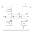
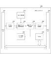
- FIG. 1 is a diagram illustrating a configuration example of an information processing system according to an embodiment of the present technology.
- This information processing system includes a host computer 100, a memory controller 200, and a memory 300.
- the memory controller 200 and the memory 300 form a memory module 400.
- the host computer 100 issues a command for instructing the memory 300 to read and write data.
- the host computer 100 includes a processor that executes processing as the host computer 100, and a controller interface for communicating with the memory controller 200.
- the memory controller 200 controls requests to the memory 300 according to commands from the host computer 100.
- the memory controller 200 is an example of the memory control device described in the claims.
- the memory 300 includes a control unit and a memory cell array.
- the control unit of the memory 300 accesses the memory cell according to the request from the memory controller 200.
- the memory cell array of the memory 300 is a memory cell array including a plurality of memory cells, and stores a binary value for each bit or a multi-valued value for each bit. A large number of memory cells are arranged in a two-dimensional form (matrix form).
- This memory cell array is assumed to be a non-volatile memory (NVM: Non-Volatile Memory) capable of overwriting data without erasing, using a page having a plurality of byte sizes (512B, for example) as an access unit for reading or writing.
- NVM Non-Volatile Memory
- FIG. 2 is a diagram illustrating a configuration example of the memory controller 200 according to the first embodiment of the present technology.
- the memory controller 200 includes a copy control unit 210, a logical address collision determination unit 230, a logical address replacement unit 240, a write request buffer 250, an address conversion unit 260, and a RAM 270.
- the memory controller 200 also includes a host interface 201 for exchanging with the host computer 100 and a memory interface 203 for exchanging with the memory 300.
- the copy control unit 210 controls copying and deletion between areas for wear leveling and the like.
- the copy control unit 210 controls read and write access in the background in addition to the processing by the command from the host computer 100. Like the access from the host computer 100, the access from the copy control unit 210 is instructed by the logical address.
- the copy operation by the copy control unit 210 is instructed in units of blocks of the memory 300.
- a block consists of multiple pages. During the copy operation, each page is processed as a copy unit. Therefore, in a block that is a copy target, there can be three types of states, that is, a page that has been copied, a page that is being copied, and a page before copying.
- the page is an example of the first storage area described in the claims.
- the block is an example of the second storage area described in the claims.
- the logical address collision determination unit 230 determines a collision between the logical address space of the area targeted for the copy operation by the copy control unit 210 and the logical address designated by the command issued from the host computer 100. is there.
- the logical address collision determination unit 230 determines the presence/absence of a collision and the state of a page when a collision occurs based on the logical addresses of both parties and the type (read or write) of a command issued from the host computer 100. (One of the above three types) is determined.
- the determination result is supplied to the logical address replacement unit 240.
- the logical address collision determination unit 230 is an example of the address collision determination unit described in the claims.
- the logical address replacement unit 240 replaces the logical address specified by the command issued from the host computer 100 with another logical address according to the determination result by the logical address collision determination unit 230. The specific content of this address replacement will be described later.
- the logical address replacement unit 240 is an example of the address replacement unit described in the claims.
- the write request buffer 250 is a buffer that holds the content of a page being copied when the write request is issued from the host computer 100 so as to wait the write request.
- the logical address conflict determination unit 230 determines that the write request is for the page being copied
- the logical address replacement unit 240 outputs the write request to the write request buffer 250.
- the address conversion unit 260 converts the logical address output from the logical address replacement unit 240 into a physical address of the memory 300.
- the address translation unit 260 holds, for example, a table that associates a logical address with a physical address, and refers to the table to translate a logical address into a physical address.
- a RAM (Random Access Memory) 270 is an internal memory that stores a work area required for the operation of the memory controller 200.
- the RAM 270 is used as a buffer area for temporarily storing the data read from the memory 300 during the copy operation for wear leveling.
- FIG. 3 is a diagram illustrating a correspondence example of the address space of the memory 300 according to the embodiment of the present technology.
- Commands issued from the host computer 100 and control of copy operations by the copy control unit 210 are instructed by logical addresses.
- the logical address space is mapped to the physical address space of the memory 300.
- the address conversion unit 260 converts the logical address into a physical address of the memory 300 in block units.
- the physical address space has a space larger than the logical address space accessible from the host computer 100. Therefore, a part of the physical address space is mapped as a logical address space inaccessible from the host computer 100.
- an area having an address lower than page #1000 in the logical address space is mapped as a “logical address space accessible from the host computer 100” (hereinafter referred to as “accessible space”).
- the area of addresses from page #1000 onward in the logical address space is mapped as a “logical address space inaccessible from the host computer 100” (hereinafter referred to as “inaccessible space”).
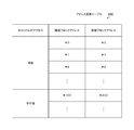
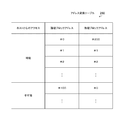
- FIG. 4 is a diagram showing a state example of a table of the address conversion unit 260 according to the embodiment of the present technology.
- FIG. 5 is a diagram showing an example of a mode of data copying in the embodiment of the present technology. This data copy is executed at the time of wear leveling and the like.
- the logical address space is copied from the accessible space to the inaccessible space.
- the data of each page of the logical block #0 is read to the RAM 270, and the read data is copied to the logical block #100. That is, the storage content of each page of the physical block #0 is copied to the physical block #200.
- the table of the address conversion unit 260 is updated so that the block copied to the inaccessible space becomes the accessible space.
- the following figure shows an example of the state.
- FIG. 6 is a diagram showing an example of the state of the table of the address conversion unit 260 after data copy according to the embodiment of the present technology.
- the physical block address corresponding to the logical block address #0 of the accessible space is updated from #0 to #200.
- the physical block address corresponding to the logical block address #100 in the inaccessible space is updated from #200 to #0. That is, the physical block addresses #0 and #200 are exchanged between the accessible space and the inaccessible space.
- the block of the copy source is once written in the inaccessible space and updated to the accessible space after the copy is completed so that it can be seen from the host computer 100. To do.
- the memory controller 200 can manage the control so that the host computer 100 does not directly see it.
- FIG. 7 is a diagram showing a state example of each page in a block when data is copied in the embodiment of the present technology.
- the copy operation by the copy control unit 210 is instructed in blocks of the memory 300.
- page-by-page copy page copy
- each page is sequentially copied from the beginning according to the copy offset indicating the copy position.
- the copy offset is incremented each time one page is copied.
- the page indicated by the copy offset is being copied, the pages before the page indicated by the copy offset have been copied, and the pages after the page indicated by the copy offset are before copying.
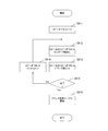
- FIG. 8 is a flowchart showing an example of a data copy processing procedure of the memory controller 200 according to the embodiment of the present technology.
- the copy offset is cleared to "0" (step S911). Then, the data is read from the page indicated by the copy offset of the copy source to the RAM 270 (step S912). The data read to the RAM 270 is written to the page indicated by the copy offset of the copy destination (step S913).
- step S914 If copying has not been completed for all pages in the block (step S914: No), the copy offset is incremented by 1 (step S915), and the processing from step S912 is repeated.
- step S914 When copying is completed for all pages in the block (step S914: Yes), the table of the address conversion unit 260 is updated (step S916), and the copy destination area is set as the accessible space.
- FIG. 9 is a diagram showing an example of a relationship between an address collision state and an operation in the embodiment of the present technology.
- the logical address collision determination unit 230 determines the state in which the access from the host computer 100 collides with the logical address space being copied. In the following, according to the figure, the case is divided into seven cases and described.
- Cases #1 to 3 are cases in which the logical address specified by the read command from the host computer 100 and the logical address space of the area targeted for the copy operation collide.
- Cases #4 to 6 are cases where the logical address specified by the write command from the host computer 100 and the logical address space of the area targeted for the copy operation collide.
- Case #7 is a case where the logical address specified by the command from the host computer 100 does not conflict with the logical address space of the area targeted for the copy operation.
- FIG. 10 is a diagram showing an operation example in cases #1 and #4 in the embodiment of the present technology.
- Case #1 is a case where the logical address designated as the read address by the host computer 100 is a copied page.
- the logical address designated as the write address by the host computer 100 is the copied page. That is, in these cases #1 and #4, the page to be accessed from the host computer 100 has already been copied. Therefore, the command from the host computer 100 can be processed by accessing the copy destination page.
- the logical address replacement unit 240 replaces the logical address specified by the command issued from the host computer 100 with the logical address of the copy destination.
- the replaced logical address is converted into a physical address by the address conversion unit 260.
- FIG. 11 is a diagram showing an operation example in the case of case #2 in the embodiment of the present technology.
- Case #2 is a case where the logical address designated as the read address by the host computer 100 is the page being copied. In this case, if the data is read from the copy source page, the read command from the host computer 100 can be processed.
- the logical address replacement unit 240 outputs the logical address specified by the command issued from the host computer 100 to the address conversion unit 260 as it is without replacement.
- the logical address that has not been replaced is translated into a physical address by the address translation unit 260.
- FIG. 12 is a diagram showing an operation example in cases #3 and #6 in the embodiment of the present technology.
- Case #3 is a case where the logical address designated as the read address by the host computer 100 is the page before copying.
- the logical address designated as the write address by the host computer 100 is the page before copying. That is, in these cases #3 and #6, the page to be accessed from the host computer 100 is not yet copied. Therefore, by accessing the copy source page, the command from the host computer 100 can be processed.
- the logical address replacement unit 240 outputs the logical address specified by the command issued from the host computer 100 to the address conversion unit 260 as it is without replacement.
- the logical address that has not been replaced is translated into a physical address by the address translation unit 260.
- FIG. 13 is a diagram showing an operation example in case #5 in the embodiment of the present technology.
- Case #5 is the case where the logical address specified as the write address by the host computer 100 is the page being copied. In this case, writing to the page being copied cannot be performed because it destroys the data.
- the logical address replacement unit 240 causes the write request buffer 250 to hold the content. Therefore, the write request is suspended until the page is in the copied state.
- the state of case #4 is reached, and the logical address replacement unit 240 replaces the logical address specified by the command issued from the host computer 100 with the logical address of the copy destination, and performs the address conversion. Output to the section 260.
- FIG. 14 is a diagram showing an operation example in case #7 in the embodiment of the present technology.
- Case #7 is a case where the logical address specified by the command from the host computer 100 does not conflict with the logical address space of the area targeted for the copy operation. Therefore, it is not necessary to perform replacement regardless of whether the command from the host computer 100 is read or write.
- the logical address replacement unit 240 outputs the logical address specified by the command issued from the host computer 100 to the address conversion unit 260 as it is without replacement.
- the logical address that has not been replaced is translated into a physical address by the address translation unit 260.
- FIG. 15 is a flowchart showing an example of a processing procedure regarding address collision determination of the memory controller 200 according to the embodiment of the present technology.
- the logical address collision determination unit 230 determines a collision between the logical address space of the copy operation area and the logical address designated by the host computer 100 ( Step S921). Then, according to the determination result, each processing is performed as follows.
- the logical address replacement unit 240 outputs the logical address specified by the command issued from the host computer 100 to the address conversion unit 260 as it is without replacement (step S935).
- the logical address that has not been replaced is translated into a physical address by the address translation unit 260 (step S939).
- the logical address replacement unit 240 replaces the logical address designated by the command issued from the host computer 100 with the logical address of the copy destination (step S936).
- the replaced logical address is converted into a physical address by the address conversion unit 260 (step S939).
- the logical address replacement unit 240 outputs the logical address specified by the command issued from the host computer 100 to the address conversion unit 260 as it is without replacement (step S935).
- the logical address that has not been replaced is translated into a physical address by the address translation unit 260 (step S939).
- step S933 If it is determined that the page to be accessed from the host computer 100 has not been copied (step S933: No), the page is being copied. At this time, if the access from the host computer 100 is a read access (step S934: Yes), it corresponds to case #2. Therefore, the logical address replacement unit 240 outputs the logical address specified by the command issued from the host computer 100 to the address conversion unit 260 as it is without replacement (step S935). The logical address that has not been replaced is translated into a physical address by the address translation unit 260 (step S939).
- step S933: No If the page to be accessed from the host computer 100 is being copied (step S933: No) and the access is not read access (step S934: No), case #5 is applicable. Therefore, the logical address replacement unit 240 causes the write request buffer 250 to hold the content and waits for the write request until the page is in the copied state (step S938). That is, the process returns to step S932 to determine that copying has been completed.
- Second Embodiment> In the above-described first embodiment, it is assumed that the access by the command from the host computer 100 is within the page. On the other hand, in the second embodiment, the case where the access by the command from the host computer 100 is not within the page is also allowed.
- the overall configuration of the information processing system is similar to that of the first embodiment described above, and detailed description thereof will be omitted.
- FIG. 16 is a diagram showing a configuration example of the memory controller 200 according to the second embodiment of the present technology.
- the memory controller 200 according to the second embodiment is different from the above-described first embodiment in that an access dividing unit 220 is further provided, and is otherwise the same.
- the access dividing unit 220 divides each area into areas that do not exceed one page if the access by the command from the host computer 100 is related to an area larger than one page. For example, if the size of one page is 512B and the access by the command from the host computer 100 is related to the data capacity of 128KB, the access is divided into 512B and supplied to the logical address collision determination unit 230. As a result, the processes after the logical address collision determination unit 230 are the same as those in the above-described first embodiment.
- the access by the command from the host computer 100 is divided into pages by the access dividing unit 220, so that even a large-sized access can be accessed page by page. Can be controlled.
- the processing procedure described in the above-described embodiment may be regarded as a method having these series of procedures, or as a program for causing a computer to execute these series of procedures or a recording medium storing the program. You can catch it.
- this recording medium for example, a CD (Compact Disc), an MD (MiniDisc), a DVD (Digital Versatile Disc), a memory card, a Blu-ray disc (Blu-ray (registered trademark) Disc), or the like can be used.
- the present technology may have the following configurations. (1) Access to the second storage area when a copy operation is being executed from a second storage area, which is a collection of a plurality of first storage areas, which is a memory copy unit, to another storage area of the memory A memory control device that controls the access in units of the first storage area when is issued. (2) An address collision determination unit that determines the address collision between the copy operation and the access in the copy unit, When it is determined in the address collision determination that the area of the copy unit to be accessed has been copied to the other storage area, the address of the area to be accessed is set to the copy destination address.
- the memory control device further comprising: (3) The address replacement unit determines that the address collision determination determines that the access is a read access and the target area of the copy unit is being copied to the other storage area. Is the memory control device according to (2), wherein the access is continued without performing the replacement. (4) The address replacement unit, when it is determined in the address collision determination that the access is a write access and the target area of the copy unit is being copied to the other storage area. Is the memory control device according to (2) or (3), in which the write access is made to wait until the area of the copy unit is already copied. (5) The memory control device according to (4), further including a write request buffer that holds the write access request while the write access is on standby.
- the address replacement unit performs the replacement when it is determined in the address collision determination that the area of the copy unit to be accessed is not copied to the other storage area. 6.
- the memory control device according to any one of (2) to (5), wherein the access is continued without being performed.
- the address replacement unit does not perform the replacement when it is determined in the address collision determination that the area of the copy unit to be accessed does not collide with the other storage area. 7.
- the memory control device according to any one of (2) to (6), wherein the access is continued.
- An address conversion unit for converting the logical address of the access target address into a physical address of the memory in units of the second storage area,
- the memory control device according to any one of (2) to (7), wherein the address conversion unit is updated to indicate a physical address after copying after the copy operation is performed.
- the other storage area is an area of a logical address space that is inaccessible before the copy operation is performed, and a logical address that is accessible in the address conversion unit after the copy operation is performed.
- the memory control device according to (8) which is updated to a space area.
- each is divided into areas not exceeding the copy unit and supplied to the address collision determination unit.
- the memory control device according to any one of (2) to (9), further comprising: (11) Memory, Access is issued to the second storage area when a copy operation is being executed from a second storage area that is a collection of a plurality of first storage areas that are copy units of the memory to another storage area of the memory. And a memory control device that controls the access in units of the first storage area. (12) The memory module according to (11), wherein the memory is a non-volatile memory.
- a host computer Memory and In the case where a copy operation is being executed from a second storage area that is a collection of a plurality of first storage areas, which is a copy unit of the memory, to another storage area of the memory, the second storage area from the host computer
- An information processing system comprising: a memory control device that controls the access in units of the first storage area when an access to the is issued.
- host computer 100 host computer 200 memory controller 201 host interface 203 memory interface 210 copy control unit 220 access division unit 230 logical address collision determination unit 240 logical address replacement unit 250 write request buffer 260 address conversion unit 300 memory 400 memory module
Landscapes
- Engineering & Computer Science (AREA)
- Theoretical Computer Science (AREA)
- Physics & Mathematics (AREA)
- General Engineering & Computer Science (AREA)
- General Physics & Mathematics (AREA)
- Human Computer Interaction (AREA)
- Techniques For Improving Reliability Of Storages (AREA)
- Memory System (AREA)
Abstract
Description
1.第1の実施の形態(ホストからのページ単位のアクセスを処理する例)
2.第2の実施の形態(ホストからのアクセスをページ単位に分割して処理する例)
[情報処理システムの構成]
図1は、本技術の実施の形態における情報処理システムの一構成例を示す図である。
図2は、本技術の第1の実施の形態におけるメモリコントローラ200の一構成例を示す図である。このメモリコントローラ200は、コピー制御部210と、論理アドレス衝突判定部230と、論理アドレス置換部240と、ライト要求バッファ250と、アドレス変換部260と、RAM270とを備える。また、このメモリコントローラ200は、ホストコンピュータ100との間のやりとりを行うためのホストインターフェース201と、メモリ300との間のやりとりを行うためのメモリインターフェース203とを備える。
図3は、本技術の実施の形態におけるメモリ300のアドレス空間の対応例を示す図である。
図5は、本技術の実施の形態におけるデータコピーの態様例を示す図である。このデータコピーは、ウェアレベリング等に際して実行されるものである。
図9は、本技術の実施の形態におけるアドレス衝突の状態と動作との関係例を示す図である。
上述の第1の実施の形態では、ホストコンピュータ100からのコマンドによるアクセスがページ内に収まっていることを前提としていた。これに対し、この第2の実施の形態では、ホストコンピュータ100からのコマンドによるアクセスがページ内に収まっていない場合も許容する。なお、情報処理システムとしての全体構成については、上述の第1の実施の形態と同様であるため、詳細な説明は省略する。
図16は、本技術の第2の実施の形態におけるメモリコントローラ200の一構成例を示す図である。この第2の実施の形態におけるメモリコントローラ200は、上述の第1の実施の形態と比べて、アクセス分割部220をさらに備える点において異なり、それ以外については同様である。
(1)メモリのコピー単位である第1の記憶領域を複数まとめた第2の記憶領域から前記メモリの他の記憶領域にコピー動作が実行されている場合において、前記第2の記憶領域に対するアクセスが発行された際に前記第1の記憶領域を単位として前記アクセスを制御するメモリ制御装置。
(2)前記コピー動作と前記アクセスとのアドレス衝突を前記コピー単位で判定するアドレス衝突判定部と、
前記アクセスの対象となる前記コピー単位の領域が前記他の記憶領域にコピー済である旨の判定が前記アドレス衝突判定においてされた場合には前記アクセスの対象となる領域のアドレスをコピー先のアドレスに置換して前記アクセスを続行させるアドレス置換部と
を具備する前記(1)に記載のメモリ制御装置。
(3)前記アドレス置換部は、前記アクセスがリードアクセスであってその対象となる前記コピー単位の領域が前記他の記憶領域にコピー中である旨の判定が前記アドレス衝突判定においてされた場合には前記置換を行わずに前記アクセスを続行させる
前記(2)に記載のメモリ制御装置。
(4)前記アドレス置換部は、前記アクセスがライトアクセスであってその対象となる前記コピー単位の領域が前記他の記憶領域にコピー中である旨の判定が前記アドレス衝突判定においてされた場合には前記コピー単位の領域がコピー済になるまで前記ライトアクセスを待機させる
前記(2)または(3)に記載のメモリ制御装置。
(5)前記ライトアクセスが待機されている間にそのライトアクセス要求を保持するライト要求バッファをさらに具備する前記(4)に記載のメモリ制御装置。
(6)前記アドレス置換部は、前記アクセスの対象となる前記コピー単位の領域が前記他の記憶領域へのコピー前である旨の判定が前記アドレス衝突判定においてされた場合には前記置換を行わずに前記アクセスを続行させる
前記(2)から(5)のいずれかに記載のメモリ制御装置。
(7)前記アドレス置換部は、前記アクセスの対象となる前記コピー単位の領域が前記他の記憶領域とは衝突しない旨の判定が前記アドレス衝突判定においてされた場合には前記置換を行わずに前記アクセスを続行させる
前記(2)から(6)のいずれかに記載のメモリ制御装置。
(8)前記第2の記憶領域を単位として前記アクセスの対象アドレスについて論理アドレスから前記メモリの物理アドレスに変換するアドレス変換部を具備し、
前記アドレス変換部は、前記コピー動作が行われた後にはコピー後の物理アドレスを示すように更新される
前記(2)から(7)のいずれかに記載のメモリ制御装置。
(9)前記他の記憶領域は、前記コピー動作が行われる前にはアクセス不可能な論理アドレス空間の領域であり、前記コピー動作が行われた後には前記アドレス変換部においてアクセス可能な論理アドレス空間の領域に更新される
前記(8)に記載のメモリ制御装置。
(10)前記第2の記憶領域に対するアクセスが前記コピー単位よりも大きい領域に関するアクセスである場合にはそれぞれが前記コピー単位を超えない領域に分割して前記アドレス衝突判定部に供給するアクセス分割部をさらに具備する前記(2)から(9)のいずれかに記載のメモリ制御装置。
(11)メモリと、
前記メモリのコピー単位である第1の記憶領域を複数まとめた第2の記憶領域から前記メモリの他の記憶領域にコピー動作が実行されている場合において、前記第2の記憶領域に対するアクセスが発行された際に前記第1の記憶領域を単位として前記アクセスを制御するメモリ制御装置と
を具備するメモリモジュール。
(12)前記メモリは、不揮発メモリである
前記(11)に記載のメモリモジュール。
(13)ホストコンピュータと、
メモリと、
前記メモリのコピー単位である第1の記憶領域を複数まとめた第2の記憶領域から前記メモリの他の記憶領域にコピー動作が実行されている場合において、前記ホストコンピュータから前記第2の記憶領域に対するアクセスが発行された際に前記第1の記憶領域を単位として前記アクセスを制御するメモリ制御装置と
を具備する情報処理システム。
200 メモリコントローラ
201 ホストインターフェース
203 メモリインターフェース
210 コピー制御部
220 アクセス分割部
230 論理アドレス衝突判定部
240 論理アドレス置換部
250 ライト要求バッファ
260 アドレス変換部
300 メモリ
400 メモリモジュール
Claims (13)
- メモリのコピー単位である第1の記憶領域を複数まとめた第2の記憶領域から前記メモリの他の記憶領域にコピー動作が実行されている場合において、前記第2の記憶領域に対するアクセスが発行された際に前記第1の記憶領域を単位として前記アクセスを制御するメモリ制御装置。
- 前記コピー動作と前記アクセスとのアドレス衝突を前記コピー単位で判定するアドレス衝突判定部と、
前記アクセスの対象となる前記コピー単位の領域が前記他の記憶領域にコピー済である旨の判定が前記アドレス衝突判定においてされた場合には前記アクセスの対象となる領域のアドレスをコピー先のアドレスに置換して前記アクセスを続行させるアドレス置換部と
を具備する請求項1記載のメモリ制御装置。 - 前記アドレス置換部は、前記アクセスがリードアクセスであってその対象となる前記コピー単位の領域が前記他の記憶領域にコピー中である旨の判定が前記アドレス衝突判定においてされた場合には前記置換を行わずに前記アクセスを続行させる
請求項2記載のメモリ制御装置。 - 前記アドレス置換部は、前記アクセスがライトアクセスであってその対象となる前記コピー単位の領域が前記他の記憶領域にコピー中である旨の判定が前記アドレス衝突判定においてされた場合には前記コピー単位の領域がコピー済になるまで前記ライトアクセスを待機させる
請求項2記載のメモリ制御装置。 - 前記ライトアクセスが待機されている間にそのライトアクセス要求を保持するライト要求バッファをさらに具備する請求項4記載のメモリ制御装置。
- 前記アドレス置換部は、前記アクセスの対象となる前記コピー単位の領域が前記他の記憶領域へのコピー前である旨の判定が前記アドレス衝突判定においてされた場合には前記置換を行わずに前記アクセスを続行させる
請求項2記載のメモリ制御装置。 - 前記アドレス置換部は、前記アクセスの対象となる前記コピー単位の領域が前記他の記憶領域とは衝突しない旨の判定が前記アドレス衝突判定においてされた場合には前記置換を行わずに前記アクセスを続行させる
請求項2記載のメモリ制御装置。 - 前記第2の記憶領域を単位として前記アクセスの対象アドレスについて論理アドレスから前記メモリの物理アドレスに変換するアドレス変換部を具備し、
前記アドレス変換部は、前記コピー動作が行われた後にはコピー後の物理アドレスを示すように更新される
請求項2記載のメモリ制御装置。 - 前記他の記憶領域は、前記コピー動作が行われる前にはアクセス不可能な論理アドレス空間の領域であり、前記コピー動作が行われた後には前記アドレス変換部においてアクセス可能な論理アドレス空間の領域に更新される
請求項8記載のメモリ制御装置。 - 前記第2の記憶領域に対するアクセスが前記コピー単位よりも大きい領域に関するアクセスである場合にはそれぞれが前記コピー単位を超えない領域に分割して前記アドレス衝突判定部に供給するアクセス分割部をさらに具備する請求項2記載のメモリ制御装置。
- メモリと、
前記メモリのコピー単位である第1の記憶領域を複数まとめた第2の記憶領域から前記メモリの他の記憶領域にコピー動作が実行されている場合において、前記第2の記憶領域に対するアクセスが発行された際に前記第1の記憶領域を単位として前記アクセスを制御するメモリ制御装置と
を具備するメモリモジュール。 - 前記メモリは、不揮発メモリである
請求項11記載のメモリモジュール。 - ホストコンピュータと、
メモリと、
前記メモリのコピー単位である第1の記憶領域を複数まとめた第2の記憶領域から前記メモリの他の記憶領域にコピー動作が実行されている場合において、前記ホストコンピュータから前記第2の記憶領域に対するアクセスが発行された際に前記第1の記憶領域を単位として前記アクセスを制御するメモリ制御装置と
を具備する情報処理システム。
Priority Applications (2)
| Application Number | Priority Date | Filing Date | Title |
|---|---|---|---|
| JP2020569368A JPWO2020158059A1 (ja) | 2019-01-31 | 2019-10-16 | メモリ制御装置、メモリモジュールおよび情報処理システム |
| KR1020217023149A KR20210118086A (ko) | 2019-01-31 | 2019-10-16 | 메모리 제어 장치, 메모리 모듈 및 정보 처리 시스템 |
Applications Claiming Priority (2)
| Application Number | Priority Date | Filing Date | Title |
|---|---|---|---|
| JP2019015647 | 2019-01-31 | ||
| JP2019-015647 | 2019-01-31 |
Publications (1)
| Publication Number | Publication Date |
|---|---|
| WO2020158059A1 true WO2020158059A1 (ja) | 2020-08-06 |
Family
ID=71839952
Family Applications (1)
| Application Number | Title | Priority Date | Filing Date |
|---|---|---|---|
| PCT/JP2019/040553 Ceased WO2020158059A1 (ja) | 2019-01-31 | 2019-10-16 | メモリ制御装置、メモリモジュールおよび情報処理システム |
Country Status (3)
| Country | Link |
|---|---|
| JP (1) | JPWO2020158059A1 (ja) |
| KR (1) | KR20210118086A (ja) |
| WO (1) | WO2020158059A1 (ja) |
Citations (2)
| Publication number | Priority date | Publication date | Assignee | Title |
|---|---|---|---|---|
| JP2008225608A (ja) * | 2007-03-09 | 2008-09-25 | Seiko Epson Corp | メモリを制御するメモリコントローラ、メモリモジュール、メモリの制御方法 |
| WO2019017017A1 (ja) * | 2017-07-18 | 2019-01-24 | ソニーセミコンダクタソリューションズ株式会社 | ウェアレベリング処理を行うメモリコントローラ |
Family Cites Families (1)
| Publication number | Priority date | Publication date | Assignee | Title |
|---|---|---|---|---|
| JP2017174387A (ja) | 2016-03-17 | 2017-09-28 | パナソニックIpマネジメント株式会社 | メモリコントローラ、不揮発性記憶装置、不揮発性記憶システム、及びメモリ制御方法 |
-
2019
- 2019-10-16 KR KR1020217023149A patent/KR20210118086A/ko not_active Abandoned
- 2019-10-16 WO PCT/JP2019/040553 patent/WO2020158059A1/ja not_active Ceased
- 2019-10-16 JP JP2020569368A patent/JPWO2020158059A1/ja not_active Abandoned
Patent Citations (2)
| Publication number | Priority date | Publication date | Assignee | Title |
|---|---|---|---|---|
| JP2008225608A (ja) * | 2007-03-09 | 2008-09-25 | Seiko Epson Corp | メモリを制御するメモリコントローラ、メモリモジュール、メモリの制御方法 |
| WO2019017017A1 (ja) * | 2017-07-18 | 2019-01-24 | ソニーセミコンダクタソリューションズ株式会社 | ウェアレベリング処理を行うメモリコントローラ |
Also Published As
| Publication number | Publication date |
|---|---|
| KR20210118086A (ko) | 2021-09-29 |
| JPWO2020158059A1 (ja) | 2021-12-02 |
Similar Documents
| Publication | Publication Date | Title |
|---|---|---|
| KR101086857B1 (ko) | 데이터 머지를 수행하는 반도체 스토리지 시스템의 제어 방법 | |
| JP5612514B2 (ja) | 不揮発性メモリコントローラ及び不揮発性記憶装置 | |
| US8055873B2 (en) | Data writing method for flash memory, and controller and system using the same | |
| JP4004468B2 (ja) | 大きなページをサポートするようにさせるための方法およびシステム | |
| US11354236B2 (en) | Garbage collection method for data storage device | |
| TWI385519B (zh) | 資料寫入方法及使用此方法的快閃儲存系統與其控制器 | |
| US7529879B2 (en) | Incremental merge methods and memory systems using the same | |
| JP5480913B2 (ja) | 記憶装置、およびメモリコントローラ | |
| US20100011154A1 (en) | Data accessing method for flash memory and storage system and controller using the same | |
| US10360155B1 (en) | Multi-tier memory management | |
| TWI579689B (zh) | 資料備份系統 | |
| JP2006216036A (ja) | フラッシュメモリを含んだデータ貯蔵装置及びそれのマージ方法 | |
| JP2008016003A (ja) | メモリー格納装置及びその読み書き方法 | |
| CN101630233B (zh) | 用于闪存的数据存取方法、储存系统与控制器 | |
| CN105718530A (zh) | 文件存储系统及其文件存储控制方法 | |
| TWI403897B (zh) | 記憶裝置及其資料管理方法 | |
| JP2010287049A (ja) | メモリシステムおよびメモリシステムの管理方法 | |
| CN113111011A (zh) | 数据存储装置及其垃圾收集方法 | |
| JP4829202B2 (ja) | 記憶装置及びメモリ制御方法 | |
| CN101996137A (zh) | 存储装置与其资料处理方法 | |
| TWI724550B (zh) | 資料儲存裝置以及非揮發式記憶體控制方法 | |
| WO2020158059A1 (ja) | メモリ制御装置、メモリモジュールおよび情報処理システム | |
| WO2016056290A1 (ja) | メモリコントローラ、メモリシステム、記憶装置、情報処理システムおよび記憶制御方法 | |
| TWI420528B (zh) | 用來增進一快閃記憶體的效能之方法以及相關之可攜式記憶裝置及其控制器 | |
| US20230019878A1 (en) | Systems, methods, and devices for page relocation for garbage collection |
Legal Events
| Date | Code | Title | Description |
|---|---|---|---|
| 121 | Ep: the epo has been informed by wipo that ep was designated in this application |
Ref document number: 19912968 Country of ref document: EP Kind code of ref document: A1 |
|
| ENP | Entry into the national phase |
Ref document number: 2020569368 Country of ref document: JP Kind code of ref document: A |
|
| ENP | Entry into the national phase |
Ref document number: 20217023149 Country of ref document: KR Kind code of ref document: A |
|
| NENP | Non-entry into the national phase |
Ref country code: DE |
|
| 122 | Ep: pct application non-entry in european phase |
Ref document number: 19912968 Country of ref document: EP Kind code of ref document: A1 |