WO2020148798A1 - 位置検出装置を備えた電子装置およびタッチ位置検出方法 - Google Patents
位置検出装置を備えた電子装置およびタッチ位置検出方法 Download PDFInfo
- Publication number
- WO2020148798A1 WO2020148798A1 PCT/JP2019/000878 JP2019000878W WO2020148798A1 WO 2020148798 A1 WO2020148798 A1 WO 2020148798A1 JP 2019000878 W JP2019000878 W JP 2019000878W WO 2020148798 A1 WO2020148798 A1 WO 2020148798A1
- Authority
- WO
- WIPO (PCT)
- Prior art keywords
- data
- value
- mutual capacitance
- self
- capacitance detection
- Prior art date
- Legal status (The legal status is an assumption and is not a legal conclusion. Google has not performed a legal analysis and makes no representation as to the accuracy of the status listed.)
- Ceased
Links
Images












Classifications
-
- G—PHYSICS
- G06—COMPUTING OR CALCULATING; COUNTING
- G06F—ELECTRIC DIGITAL DATA PROCESSING
- G06F3/00—Input arrangements for transferring data to be processed into a form capable of being handled by the computer; Output arrangements for transferring data from processing unit to output unit, e.g. interface arrangements
- G06F3/01—Input arrangements or combined input and output arrangements for interaction between user and computer
- G06F3/03—Arrangements for converting the position or the displacement of a member into a coded form
- G06F3/041—Digitisers, e.g. for touch screens or touch pads, characterised by the transducing means
- G06F3/0416—Control or interface arrangements specially adapted for digitisers
- G06F3/04166—Details of scanning methods, e.g. sampling time, grouping of sub areas or time sharing with display driving
- G06F3/041662—Details of scanning methods, e.g. sampling time, grouping of sub areas or time sharing with display driving using alternate mutual and self-capacitive scanning
-
- G—PHYSICS
- G06—COMPUTING OR CALCULATING; COUNTING
- G06F—ELECTRIC DIGITAL DATA PROCESSING
- G06F1/00—Details not covered by groups G06F3/00 - G06F13/00 and G06F21/00
- G06F1/16—Constructional details or arrangements
- G06F1/1613—Constructional details or arrangements for portable computers
- G06F1/1633—Constructional details or arrangements of portable computers not specific to the type of enclosures covered by groups G06F1/1615 - G06F1/1626
- G06F1/1637—Details related to the display arrangement, including those related to the mounting of the display in the housing
- G06F1/1652—Details related to the display arrangement, including those related to the mounting of the display in the housing the display being flexible, e.g. mimicking a sheet of paper, or rollable
-
- G—PHYSICS
- G06—COMPUTING OR CALCULATING; COUNTING
- G06F—ELECTRIC DIGITAL DATA PROCESSING
- G06F3/00—Input arrangements for transferring data to be processed into a form capable of being handled by the computer; Output arrangements for transferring data from processing unit to output unit, e.g. interface arrangements
- G06F3/01—Input arrangements or combined input and output arrangements for interaction between user and computer
- G06F3/03—Arrangements for converting the position or the displacement of a member into a coded form
- G06F3/041—Digitisers, e.g. for touch screens or touch pads, characterised by the transducing means
- G06F3/0412—Digitisers structurally integrated in a display
-
- G—PHYSICS
- G06—COMPUTING OR CALCULATING; COUNTING
- G06F—ELECTRIC DIGITAL DATA PROCESSING
- G06F3/00—Input arrangements for transferring data to be processed into a form capable of being handled by the computer; Output arrangements for transferring data from processing unit to output unit, e.g. interface arrangements
- G06F3/01—Input arrangements or combined input and output arrangements for interaction between user and computer
- G06F3/03—Arrangements for converting the position or the displacement of a member into a coded form
- G06F3/041—Digitisers, e.g. for touch screens or touch pads, characterised by the transducing means
- G06F3/0416—Control or interface arrangements specially adapted for digitisers
- G06F3/0418—Control or interface arrangements specially adapted for digitisers for error correction or compensation, e.g. based on parallax, calibration or alignment
-
- G—PHYSICS
- G06—COMPUTING OR CALCULATING; COUNTING
- G06F—ELECTRIC DIGITAL DATA PROCESSING
- G06F3/00—Input arrangements for transferring data to be processed into a form capable of being handled by the computer; Output arrangements for transferring data from processing unit to output unit, e.g. interface arrangements
- G06F3/01—Input arrangements or combined input and output arrangements for interaction between user and computer
- G06F3/03—Arrangements for converting the position or the displacement of a member into a coded form
- G06F3/041—Digitisers, e.g. for touch screens or touch pads, characterised by the transducing means
- G06F3/044—Digitisers, e.g. for touch screens or touch pads, characterised by the transducing means by capacitive means
- G06F3/0446—Digitisers, e.g. for touch screens or touch pads, characterised by the transducing means by capacitive means using a grid-like structure of electrodes in at least two directions, e.g. using row and column electrodes
Definitions
- the following disclosure relates to an electronic device (for example, an organic EL display device) including a position detection device and a touch position detection method.
- an electronic device for example, an organic EL display device
- a position detection device for example, a touch position detection method
- organic EL display devices equipped with pixel circuits including organic EL elements have been put into practical use.
- the organic EL element is also called an OLED (Organic Light-Emitting Diode), and is a self-luminous display element that emits light with brightness according to the current flowing through it. Since the organic EL element is a self-luminous display element as described above, the organic EL display device can easily be made thinner than a liquid crystal display device that requires a backlight, a color filter, and the like.
- a technique of providing a touch panel on the surface of a panel has been put into practical use. Examples of organic EL display devices with a touch panel include smartphones and tablet terminals.
- touch position detection accuracy is improved.
- Both the self-capacitance method and the mutual capacitance method are position detection methods by the electrostatic capacity method.
- the self-capacitance method is a method of measuring the position of the recognition target object by detecting that the capacitance increases due to contact or approach of the recognition target object to the touch panel.
- the mutual capacitance method is a method of measuring the position of the recognition target object based on a difference in capacitance between adjacent sensors caused by contact or approach of the recognition target object to the touch panel.
- Japanese Unexamined Patent Publication No. 2017-187946 also discloses a touch panel that detects a touch position by combining self-capacitance sensing and mutual capacitance sensing.
- the sensor sensitivity is determined according to the distance between the recognition target and the sensor electrode.
- the distance between the recognition target and the sensor electrode is determined by the thickness of a member such as a cover material arranged on the sensor electrode.
- a detection result (appropriate detection result) as shown in, for example, FIG. 25 is obtained for a certain row.
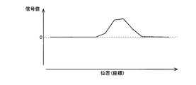
- the contact surface of the finger and the sensor electrode are located at an extremely short distance (for example, a distance of 0.1 mm or less). Further, since the cover film has flexibility, the member may be deformed when touched. Furthermore, the coupling (capacitive coupling) between the sensor electrode adjacent to the sensor electrode corresponding to the touch position (hereinafter referred to as "adjacent sensor electrode") and the finger may occur. From the above, when mutual capacitance sensing is performed, a detection result as shown in FIG. 26 may be obtained for a certain row. In FIG. 26, the signal value as the detection result is a negative value in the range of the arrow with the reference numeral 91.
- such a signal having a negative value (negative value data) generated during sensing is hereinafter referred to as a “negative signal”. Since the conventional configuration does not assume the occurrence of such a negative signal, the touch position cannot be correctly specified when the negative signal occurs.
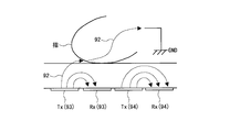
- FIG. 27 is a diagram for explaining the flow of electricity when there is a sufficient gap between the finger and the sensor electrode.
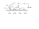
- FIG. 28 is a diagram for explaining the flow of electricity when the distance between the finger and the sensor electrode is extremely short.
- the sensor electrode includes a transmitting electrode Tx and a receiving electrode Rx. 27 and 28, the transmitter electrode Tx (93) and the receiver electrode Rx (93) are sensor electrodes corresponding to the touch position, and the transmitter electrode Tx (94) and the receiver electrode Rx (94) are adjacent to each other. It is a sensor electrode.
- the transmission side electrode Tx (93) corresponding to the touch position passes through the finger and the human body. Electricity flows to the ground GND. As a result, there is a difference between the amount of electricity flowing from the transmitting side electrode Tx (93) to the receiving side electrode Rx (93) and the amount of electricity flowing from the transmitting side electrode Tx (94) to the receiving side electrode Rx (94). Occurs. This difference appears as a positive value in the detection signal.
- a negative signal may occur during mutual capacitance sensing.
- the in-plane distribution of signal values (signal values as detection results) is disturbed. Since the touch position is typically obtained by calculating the center of gravity based on the in-plane distribution of signal values, the touch position cannot be correctly obtained if the in-plane distribution of signal values is disturbed. As a result, the touch position detection accuracy deteriorates.
- the following disclosure aims to realize an electronic device equipped with a position detection device that can detect a touch position with high accuracy even if the device becomes thinner.
- An electronic device is an electronic device including a display panel that displays an image and a position detection device that detects a touch position, The position detection device, A touch panel provided on the surface of the display panel, A touch panel drive circuit that drives the touch panel so that the touch position is detected by both a self-capacitance method and a mutual capacitance method; A touch position, including a self-capacitance detection data that is the data detected by the self-capacitance method, and a position detection circuit that specifies based on the mutual capacitance detection data that is the data detected by the mutual capacitance method, The position detection circuit, When the mutual capacitance detection data includes negative value data, Mutual capacitance detection area including a negative value data area in which negative value data is detected by the mutual capacitance method and a positive value data area adjacent to the negative value data area and in which positive value data is detected by the mutual capacitance method, and a self-capacity method If there is an area where the self-capacity detection area where significant
- a touch position detection method is a touch position detection method by a position detection device capable of detecting a touch position by both a self-capacitance method and a mutual capacitance method, A first determination step of determining whether or not negative value data is included in the mutual capacitance detection data, which is the data detected by the mutual capacitance method, When it is determined in the first determination step that the mutual capacitance detection data includes negative value data, the negative value data region in which the negative value data is detected by the mutual capacitance method is adjacent to the negative value data region.
- an electronic device such as an organic EL display device or a liquid crystal display device
- a position detection device that can detect a touch position with high accuracy can be realized even if the device becomes thinner.
- FIG. 4 is a diagram for explaining a self-capacity detection area in the above embodiment.
- FIG. 6 is a diagram showing an example of how the self-capacity detection area, the negative value data area, and the positive value data area overlap in the above embodiment. 6 is a flowchart showing a schematic procedure of processing for position detection in the embodiment.
- it is a figure showing an example of a three-dimensional map based on mutual capacitance sensing when signal collapse has occurred. It is a graph which shows the difference with the target size of the signal level (signal level about the X-axis direction) obtained by self-capacitance sensing. It is a graph showing "the relationship between a target size and a signal level" based on FIG.
- FIG. 15 It is a graph which shows the difference with the target size of the signal level (signal level about the Y-axis direction) obtained by self-capacity sensing.
- 16 is a graph showing the “relationship between target size and signal level” based on FIG. 15.
- 6 is a flowchart showing a detailed procedure of a correction process in the above embodiment.
- it is a figure showing an example of a three-dimensional map based on mutual capacitance detection data before execution of the 1st amendment processing.
- FIG. 9 is a diagram showing an example of data obtained by normalizing the data shown in FIG. 7 in the embodiment. It is a figure for demonstrating the 2nd correction process in the said embodiment. In the above-mentioned embodiment, it is a figure showing an example of a three-dimensional map based on mutual capacitance detection data after execution of the 2nd amendment processing.
- FIG. 14 is a diagram showing an example of a three-dimensional map based on mutual capacitance detection data after execution of second correction processing in the modification of the embodiment. It is a perspective view of a foldable ultra-thin display. It is a figure which shows an example of the detection result when mutual capacitance sensing is performed when there is an appropriate space between the contact surface of the finger and the sensor electrode.
- an organic EL display device will be described as an example of an electronic device including a touch panel.
- m, n, M, and N are integers of 2 or more
- i is an integer of 1 or more and n or less
- j is an integer of 1 or more and m or less.
- the detection data obtained by self-capacity sensing is called “self-capacity detection data”
- the detection data obtained by mutual capacitance sensing is called “mutual capacitance detection data”.
- FIG. 2 is a block diagram showing the configuration of the organic EL display device 10 according to the embodiment.
- the organic EL display device 10 includes an organic EL panel (display panel) 11, a display control circuit 12, a scanning line drive circuit 13, a data line drive circuit 14, a power supply circuit 15, a touch panel 20, and a touch panel controller 30.
- the touch panel 20 is provided on the surface of the organic EL panel 11.
- the surface of the touch panel 20 is formed of a film-shaped cover material called “cover film”, “window film”, or the like. Further, the organic EL panel 11 and the touch panel 20 have flexibility. That is, the organic EL display device 10 according to the present embodiment is a foldable, ultra-thin display with a touch panel.
- the organic EL panel 11 includes n scanning lines G1 to Gn, m data lines D1 to Dm, and (m ⁇ n) pixel circuits 17.
- the scanning lines G1 to Gn are arranged in parallel with each other.
- the data lines D1 to Dm are arranged in parallel with each other.
- the scanning lines G1 to Gn and the data lines D1 to Dm are orthogonal to each other.
- the (m ⁇ n) pixel circuits 17 are arranged corresponding to the intersections of the scanning lines G1 to Gn and the data lines D1 to Dm.
- the display control circuit 12 outputs control signals CS1, CS2, CS3, and CS4 to the scanning line drive circuit 13, the data line drive circuit 14, the power supply circuit 15, and the touch panel controller 30, respectively.
- the display control circuit 12 also outputs the video signal DV input from the outside of the organic EL display device 10 to the data line drive circuit 14. At that time, the video signal DV may be appropriately corrected.
- the scanning line driving circuit 13 drives the scanning lines G1 to Gn based on the control signal CS1.
- the data line driving circuit 14 drives the data lines D1 to Dm based on the control signal CS2 and the video signal DV. More specifically, in each line period, the scanning line driving circuit 13 selects one scanning line from the n scanning lines G1 to Gn and selects the selected voltage (selection voltage (in the pixel circuit 17)). The voltage at which the write control transistor turns on is applied. As a result, m pixel circuits 17 connected to the selected scanning line are collectively selected.
- the data line drive circuit 14 applies m data voltages corresponding to the video signal DV to the data lines D1 to Dm, respectively. As a result, m data voltages are respectively written in the selected m pixel circuits.
- the scanning line drive circuit 13 is formed in the organic EL panel 11 together with the pixel circuit 17.
- a common electrode (not shown in FIG. 2) which is an electrode for supplying a low level power supply voltage ELVSS common to the (m ⁇ n) pixel circuits 17, and the (m ⁇ n).
- a power supply line 18 for supplying the high level power supply voltage ELVDD is formed to each pixel circuit 17.
- the power supply circuit 15 applies the low-level power supply voltage ELVSS to the common electrode and the high-level power supply voltage ELVDD to the power supply wiring 18 based on the control signal CS3.
- the touch panel controller 30 includes a touch panel drive circuit 31 and a position detection circuit 32.
- the touch panel controller 30 controls the operation of the touch panel 20.
- the touch panel drive circuit 31 provides the touch panel 20 with a drive signal SD for detecting the touch position based on the control signal CS4 provided from the display control circuit 12.
- a configuration is adopted in which the touch position can be detected by both the self-capacitance method and the mutual capacitance method. That is, the touch panel drive circuit 31 drives the touch panel 20 so that the touch position is detected by both the self-capacitance method and the mutual capacitance method.
- the position detection circuit 32 identifies the position where the touch panel 20 is touched based on the detection signal SX. More specifically, the mutual capacitance detection data and the self capacitance detection data are obtained from the detection signal SX, and the position detection circuit 32 specifies the touch position based on the self capacitance detection data and the mutual capacitance detection data (however, as will be described later). Finally, the final identification of the touch position is based on mutual capacitance detection data only). Then, the touch panel controller 30 gives a control signal (position signal) PS to the display control circuit 12 so that processing corresponding to the touch position is performed.
- the touch panel 20 and the touch panel controller 30 implement a position detection device.
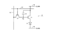
- FIG. 3 is a circuit diagram of the pixel circuit 17 on the i-th row and the j-th column.
- the pixel circuit 17 includes a transistor (driving transistor) T1, a transistor (writing control transistor) T2, a capacitor C1, and an organic EL element L1.
- the organic EL element L1 is an electro-optical element that emits any color of red, green, and blue.
- the transistors T1 and T2 are N-channel thin film transistors (TFTs).
- TFTs thin film transistor using an oxide semiconductor for a channel layer
- an amorphous silicon TFT, or the like can be used.
- the oxide TFT include a TFT containing InGaZnO (indium gallium zinc oxide).
- the oxide TFT By adopting the oxide TFT, for example, high definition and low power consumption can be achieved.
- the transistor T2 the level relationship of the potentials of the two terminals other than the gate terminal (control terminal) is switched depending on the state. Therefore, regarding the transistor T2, one of the two terminals other than the gate terminal is referred to as a "first conduction terminal”, and the other is referred to as a "second conduction terminal”.
- the gate terminal of the transistor T1, the second conduction terminal of the transistor T2, and one end of the capacitor C1 are connected to each other.
- An area (wiring) where these are connected to each other is called a "control node".
- the control node is denoted by Na.
- the gate terminal is connected to the control node Na
- the drain terminal is connected to the power supply wiring 18 to which the high-level power supply voltage ELVDD is applied
- the source terminal is connected to the anode terminal of the organic EL element L1.
- the gate terminal is connected to the scanning line Gi
- the first conduction terminal is connected to the data line Dj
- the second conduction terminal is connected to the control node Na.
- the capacitor C1 one end is connected to the control node Na and the other end is connected to the drain terminal of the transistor T1.
- the organic EL element L1 the anode terminal is connected to the source terminal of the transistor T1, and the cathode terminal is connected to the common electrode 19 to which the low level power supply voltage ELVSS is applied.
- the transistor T2 When the voltage of the scanning line Gi becomes high level, the transistor T2 is turned on and the voltage of the data line Dj is applied to the control node Na. When the voltage of the scanning line Gi becomes low level, the transistor T2 is turned off. When the transistor T2 is turned off, the control node Na is in a floating state, and the capacitor C1 holds the gate-drain voltage of the transistor T1.
- the drive current flowing through the transistor T1 and the organic EL element L1 changes according to the gate-source voltage of the transistor T1.
- the organic EL element L1 emits light with a brightness according to the magnitude of the drive current. In this way, the organic EL element L1 in each pixel circuit 17 emits light to display an image on the organic EL panel 11.
- the configuration of the pixel circuit 17 shown in FIG. 3 is an example, and pixel circuits having various configurations can be adopted.
- FIG. 4 is an example of a plan view of the touch panel 20.
- the touch panel 20 shown in FIG. 4 includes N drive lines (transmission side electrodes) Tx1 to TxN and M sense lines (reception side electrodes) Rx1 to RxM as sensor electrodes.
- the drive lines Tx1 to TxN are arranged in parallel with each other.
- the sense lines Rx1 to RxM are arranged in parallel with each other.
- the drive lines Tx1 to TxN and the sense lines Rx1 to RxM are orthogonal to each other.
- the self-capacitance sensing all drive lines Tx1 to TxN and all sense lines Rx1 to RxM are driven simultaneously.
- N drive lines Tx1 to TxN are driven one by one with all sense lines Rx1 to RxM turned on.
- the touch panel 20 may be composed of sensor electrodes called a diamond pattern as shown in FIG.
- a configuration in which the transmission side electrode Tx and the reception side electrode Rx are formed in different layers a configuration in which the transmission side electrode Tx and the reception side electrode Rx are formed in the same layer, and a configuration called a metal mesh type (as in the conventional case) It is possible to adopt a configuration in which silver or copper is used instead of the ITO film).
- the touch position can be detected by both the self-capacitance method and the mutual capacitance method.
- a negative signal negative value data
- a negative signal does not occur during self-capacity sensing. Therefore, when a negative signal is generated by the mutual capacitance sensing, the mutual capacitance detection data is corrected using the self capacitance detection data. Then, the center of gravity is calculated based on the corrected mutual capacitance detection data (original mutual capacitance detection data when correction is unnecessary) to finally specify the touch position. Note that noise and the like are included in the detection data for both mutual capacitance sensing and self-capacitance sensing.
- a threshold value for removing noise or the like is set in advance, and the processing is performed by ignoring data less than the threshold value. That is, the detection data whose value is equal to or more than the threshold value (self-capacity detection data, mutual capacitance detection data) is treated as significant data (data used to identify the touch position), and the detection data whose value is less than the threshold value. Is treated as insignificant data (data that is not used to identify the touch position). Regarding the detection data, values above the threshold are treated as significant values, and values below the threshold are treated as insignificant values.
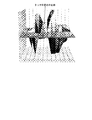
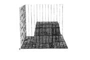
- FIG. 6 is a diagram showing the detection result of the mutual capacitance sensing in a three-dimensional form (hereinafter, such a diagram is referred to as a “three-dimensional map”).
- the part denoted by reference numeral 51 represents that a negative signal is generated.
- a region in which such a negative signal is generated is called a “negative value data region”.
- An area in which a positive value (positive value data) is obtained as the detection result of the mutual capacitance sensing is referred to as a “positive value data area”.
- An area including a negative value data area and a positive value data area is referred to as a "mutual capacitance detection area”.
- the detection result of self-capacitance sensing is obtained for each drive line and each sense line. That is, the signal value as the detection result is obtained for each coordinate in the X-axis direction and also for each coordinate in the Y-axis direction.
- the signal value of each coordinate in the X-axis direction is normalized so that the sum of the signal values of all coordinates in the X-axis direction is set to 1. Normalization is performed by setting the sum of the signal values of all coordinates of 1 to 1. By multiplying the normalized signal value of each coordinate in the X-axis direction by the normalized signal value of each coordinate in the Y-axis direction, three-dimensional data based on self-capacity sensing is generated.
- FIG. 9 An example of a part of this three-dimensional data is shown in FIG. Further, an example of a three-dimensional map based on the three-dimensional data is shown in FIG.
- the value of the three-dimensional data obtained as described above is compared with a threshold value, and data having a value equal to or greater than the threshold value is determined to be significant data.
- the area where such significant data is obtained by the self-capacity sensing is referred to as "self-capacity detection area".
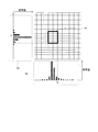
- a signal value such as a portion denoted by reference numeral 52 in the X-axis direction is obtained, and a signal value such as a portion denoted by reference numeral 53 in the Y-axis direction is obtained.
- the area within the thick line with reference numeral 54 becomes the self-capacity detection area.
- the self-capacity detection area as described above is determined by the position detection circuit 32. Further, for example, the X axis direction corresponds to the first axis direction, and the Y axis direction corresponds to the second axis direction. Further, the threshold value to be compared with the value of the three-dimensional data corresponds to the fourth threshold value.
- FIG. 10 is a diagram showing an example of how the self-capacity detection area, the negative value data area, and the positive value data area overlap.
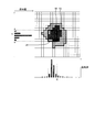
- the area inside the thick line with reference numeral 56 is the positive value data area.
- the area excluding the positive value data area (the area within the thick line with the reference numeral 56) in the area within the thick line with the reference numeral 55 is the negative value data area. Since the mutual capacitance detection region is a region composed of a negative value data region and a positive value data region, the region within the thick line with the reference numeral 55 is the mutual capacitance detection region.
- the touch panel drive circuit 31 gives a drive signal SD for mutual capacitance sensing to the touch panel 20 (step S10). Then, the position detection circuit 32 receives the detection signal SX (step S20). Next, the touch panel drive circuit 31 gives the drive signal SD for mutual capacitance sensing to the touch panel 20 again (step S30). Then, the position detection circuit 32 receives the detection signal SX (step S40).
- the phase of the drive signal SD is different between step S10 and step S30.
- the touch panel drive circuit 31 gives a drive signal SD for self-capacity sensing to the touch panel 20 (step S50).
- the position detection circuit 32 receives the detection signal SX (step S60).
- the position detection circuit 32 determines the position based on the detection signal SX acquired in step S20, step S40, and step S60 (determines the presence/absence of a touch to determine the touch position. (Identifying process) is performed (step S70).
- Position identification processing> ⁇ 2.3.1 Procedure> Next, the position specifying process (the process of step S70 of FIG. 11) will be described in detail with reference to the flowchart shown in FIG. This position identification processing is performed by the position detection circuit 32 in the touch panel controller 30.
- step S700 After starting the position specifying process, first, it is determined whether or not a touch signal is detected (step S700).
- the touch signal here means a significant change in the detection signal SX.
- step S700 if the touch signal is detected, the process proceeds to step S710, and if the touch signal is not detected, the position specifying process ends.
- step S710 it is determined whether or not the mutual capacitance detection data includes a negative signal (negative value data). As a result, if it is determined that the mutual capacitance detection data does not include a negative signal, the process proceeds to step S715, and if it is determined that the mutual capacitance detection data includes a negative signal, the process proceeds. It proceeds to step S720.
- step S715 the touch position is calculated (specified) by calculating the center of gravity using the value of the mutual capacitance detection data as it is.
- step S720 it is determined whether or not there is a region where the mutual capacitance detection region and the self capacitance detection region overlap. In other words, it is determined whether or not there is a region in which significant data as self-capacity detection data is detected in the mutual capacitance detection region. As a result, if it is determined that there is a region where the mutual capacitance detection region and the self capacitance detection region overlap, the process proceeds to step S730. On the other hand, if it is determined that there is no area where the mutual capacitance detection area and the self-capacity detection area overlap, it is considered that the touch signal is detected due to the water droplets, and this position is determined without specifying the touch position. The specific process ends.
- step S730 it is determined whether correction processing is necessary. Specifically, it is determined whether the maximum absolute value of the negative signal and the size (area) of the negative value data area are each equal to or greater than a predetermined threshold, and the maximum absolute value of the negative signal is determined. If both the value and the size (area) of the negative value data area are equal to or larger than the predetermined threshold value, it is determined that the correction process is necessary. If the result of determination in step S730 is that correction processing is required, the processing proceeds to step S740, and if it is determined that correction processing is not required, processing proceeds to step S735.
- the threshold value to be compared with the maximum absolute value of the negative signal corresponds to the second threshold value
- the threshold value to be compared with the size (area) of the negative value data area corresponds to the third threshold value. To do.
- step S735 the touch position is calculated (specified) by calculating the center of gravity using the value of the mutual capacitance detection data as it is. That is, the touch position is calculated using the value of the mutual capacitance detection data for the positive value data region and the value of the mutual capacitance detection data for the negative value data region as they are. Note that the touch position may be calculated using the corrected mutual capacitance detection data by performing the same correction process as the later-described first correction process on the mutual capacitance detection data.
- step S740 a correction process is performed to correct the mutual capacitance detection data based on the self capacitance detection data so that the influence of the negative signal is removed. A detailed description of the correction process will be given later.
- step S750 the touch position is calculated (specified) by performing the center of gravity calculation using the corrected mutual capacitance detection data obtained by the correction processing in step S740.
- step S760 output of the touch position specified in any of steps S715, S735, and S750 (output of control signal PS indicating the specified touch position) is performed. As a result, the position specifying process ends.
- the position detection circuit 32 detects the negative signal (negative value data) in the mutual capacitance sensing when the negative signal (negative value data) is included in the mutual capacitance detection data.
- the mutual capacitance detection area consisting of the positive value data area adjacent to the negative value data area where the positive value data is detected by the mutual capacity sensing and the self capacitance detection area where the significant data is detected by the self capacity sensing overlap. If there is an area (however, the maximum value of the absolute value of the negative signal and the size of the negative value data area are equal to or greater than the threshold value), a correction process is performed to correct the mutual capacitance detection data based on the self capacitance detection data.
- the touch position is specified based on the mutual capacitance detection data after the correction process.
- the position detection circuit 32 specifies the touch position based on only the mutual capacitance detection data without using the self capacitance detection data.
- step S710 implements the first determination step
- step S720 implements the second determination step
- step S730 implements the third determination step
- step S740 implements the correction step.
- the touch position specifying step is realized by step S750.
- the detection signal obtained with a capacitive touch panel changes depending on whether the ground potential when the human body is regarded as a conductor and the ground potential of the touch panel are common.
- the detection signal also changes depending on the target size (touch area of the recognition target).
- the ground potential when the human body is regarded as a conductor and the ground potential of the touch panel are not common (floating state) (for example, when an electronic device with a touch panel is not connected to an AC power source such as a smartphone) ), it is difficult for static electricity to flow from the touch panel to the human body, and when a large finger is touched in such a floating state, an electric current different from the original flow occurs.
- the mutual capacitance sensing provides mutual capacitance detection data whose three-dimensional map is represented as shown in FIG. 12, for example.
- the data at the center of the touch position is data that is inappropriate for specifying the touch position (hereinafter, simply referred to as “improper data”). Such a state is called "signal collapse”.
- the negative signal When the negative signal is generated but the signal collapse is not generated as in the example shown in FIG. 6, the negative signal is ignored because the data at the center of the touch position is not inappropriate data. It is considered that the influence of the negative signal can be removed by correcting the value of the mutual capacitance detection data for the value data area to 0, for example.
- the negative signal when the negative signal is generated and the signal collapse is also generated as in the example shown in FIG. 12, the data in the central portion of the touch position is improper data, and thus the negative value data area is set.
- the touch position cannot be accurately obtained only by correcting the value of the mutual capacitance detection data of 0 to 0. Therefore, two correction methods are prepared as described above.
- signal decay occurs when the target size is large, so it is preferable to determine the correction method based on the size of the target size.
- the size of the target size can be determined from the detection result of the self-capacitance sensing. This will be described below.
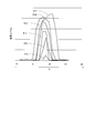
- FIG. 13 is a graph showing the difference in signal level (signal level in the X-axis direction) obtained by self-capacitance sensing depending on the target size.
- the polygonal lines denoted by reference numerals 61a, 61b, 61c, 61d, 61e, and 61f represent data having target sizes (diameters) of 4 mm, 8 mm, 12 mm, 16 mm, 20 mm, and 30 mm, respectively.
- FIG. 14 is a graph showing the “relationship between target size and signal level” based on FIG.
- FIG. 15 is a graph showing the difference in signal level (signal level in the Y-axis direction) obtained by self-capacitance sensing depending on the target size.
- the polygonal lines with reference numerals 62a, 62b, 62c, 62d, 62e, and 62f represent data with target sizes (diameters) of 4 mm, 8 mm, 12 mm, 16 mm, 20 mm, and 30 mm, respectively.
- FIG. 16 is a graph showing the “relationship between target size and signal level” based on FIG. It is understood from FIGS. 13 to 16 that the signal level increases as the target size increases. That is, the size of the target size can be determined based on the signal level. As described above, the size of the target size can be determined from the detection result of the self-capacitance sensing.
- a correction process for correcting the value of the mutual capacitance detection data is performed while switching between the two correction methods according to the detection result of the self-capacity sensing.
- the detailed procedure of the correction process will be described with reference to the flowchart shown in FIG.
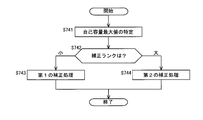
- the maximum value of the self-capacity detection data in the mutual capacitance detection area (hereinafter referred to as “self-capacity maximum value”) is specified (step S741). Since the detection signal SX is obtained for each drive line and each sense line during the self-capacitance sensing, the maximum value for the drive line (hereinafter referred to as the “first axis maximum value”) is set as the maximum value of the self-capacitance in step S741. ) And the maximum value for the sense line (hereinafter referred to as the “second axis maximum value”).
- the correction rank for determining the correction method is determined based on the maximum value of the self capacity (step S742).
- two correction ranks “large” and “small” are prepared.
- the correction rank "large” is associated with the correction method when the target size is large
- the correction rank "small” is associated with the correction method when the target size is small.
- the maximum value of the first axis and the maximum value of the second axis are compared with a threshold value prepared in advance. If the first axis maximum value is less than or equal to the threshold value and the second axis maximum value is less than or equal to the threshold value, the target size is considered to be small, and thus the correction rank is determined as “small”.
- the target size is considered to be large, and thus the correction rank is determined as “large”. If it is determined that the correction rank is “small”, the process proceeds to step S743, and if it is determined that the correction rank is “large”, the process proceeds to step S744.
- the correction rank may be determined by comparing the area of the self-capacity detection area with a threshold value. Further, the correction rank may be determined based on the value at the position of the center of gravity obtained based on the self-capacity detection data and the area of the self-capacity detection region. Furthermore, although an example in which two correction methods are prepared is shown here, three or more correction methods are prepared, a multi-step threshold value is provided, and correction is performed by an appropriate correction method according to the target size. You may want to be told.
- the first correction process which is the correction process corresponding to the correction rank "small" is performed.
- the first correction process is a process associated with the case where the target size is small, and typically, the range is extremely narrow even when no signal decay occurs or even if signal decay occurs. If done.
- the value of the mutual capacitance detection data for the negative value data area is corrected to a predetermined value (fixed value) of 0 or more.
- the predetermined value is set to a value equal to or smaller than a predetermined threshold value (for example, “0”) so that it is processed as if a significant detection signal was not obtained. That is, it is preferable to set an insignificant value as the value of the mutual capacitance detection data to the above predetermined value.
- the three-dimensional map based on the mutual capacitance detection data changes from, for example, that shown in FIG. 18 to that shown in FIG.
- a second correction process which is a correction process corresponding to the correction rank "large" is performed.
- the second correction process is a process associated with a large target size, and is typically performed when the signal collapse occurs in a wide range.
- the self-capacitance detection data is used to correct the mutual capacitance detection data so that the corrected three-dimensional map has a mountain shape. Specifically, first, all the values of the mutual capacitance detection data are rewritten to "0". Then, the self-capacity detection data is set so that the maximum value of the self-capacity detection data becomes equal to the maximum value that the mutual capacitance detection data can take (for example, “1024” if the mutual capacitance detection data is 10-bit data).
- Normalization is applied to all values.
- the data shown in FIG. 7 becomes the data shown in FIG. 20 by normalization.
- each value of the mutual capacitance detection data is rewritten with the value of the corresponding position in the normalized self capacitance detection data.
- the mutual capacitance detection area and the self capacitance detection area become equal.
- the second correction processing causes “ The value of the mutual capacitance detection data is corrected so as to satisfy the relationship of “signal value of the area with reference numeral 71>signal value of the area with reference numeral 72>signal value of the area with reference numeral 73”.
- the three-dimensional map based on the mutual capacitance detection data is changed from, for example, that shown in FIG. 12 to that shown in FIG.
- a method of correcting the value of the mutual capacitance detection data in the negative value data area to a predetermined value of 0 or more (first correction processing)
- First correction processing Normalize the self-capacitance detection data so that the maximum value of the self-capacitance detection data for the mutual capacitance detection area including the negative value data area is equal to the maximum possible value of the mutual capacitance detection data
- second correction processing A combination with a method of correcting each value of the capacitance detection data to a value at a corresponding position in the normalized self-capacity detection data.
- the self-capacity detection data is used to correct the mutual capacitance detection data so that the corrected three-dimensional map has a shape close to a truncated pyramid.
- the value of the mutual capacitance detection data for the area other than the self-capacity detection area is rewritten to a value equal to or less than a predetermined threshold value (this threshold value corresponds to the first threshold value).
- this threshold value corresponds to the first threshold value.
- the value of the mutual capacitance detection data for the region other than the self-capacity detection region is rewritten to, for example, “0” so that it is processed as if a significant detection signal was not obtained.
- the value of the mutual capacitance detection data for the self-capacity detection region is corrected to a predetermined value (fixed value) equal to or more than the threshold value.
- the threshold value be set to a value that is a boundary between a significant value and an insignificant value with respect to the value of the mutual capacitance detection data.
- the predetermined value is set to a value equal to the maximum value that the mutual capacitance detection data can take (for example, “1024” if the mutual capacitance detection data is 10-bit data).
- the reason why the shape of the corrected three-dimensional map is not a rectangular parallelepiped but a shape close to a quadrangular pyramid is that the value of the area on one side of the boundary is represented in the boundary portion where the value (value of the three-dimensional data) changes.
- the line connecting the coordinate (coordinate in the three-dimensional space) and the coordinate representing the value of the area on the other side of the boundary (the coordinate in the three-dimensional space) is not perpendicular to the plane having the value 0. Because.
- the second correction is performed.
- the value becomes a predetermined value (fixed value) equal to or more than the threshold value for the area within the thick line denoted by reference numeral 54 in FIG. 9, and the value becomes “0” for the other areas, for example.
- the value of the mutual capacitance detection data is corrected. Therefore, in this modification, the three-dimensional map based on the mutual capacitance detection data changes from that shown in FIG. 12 to that shown in FIG. 23, for example.
- a method of correcting the value of the mutual capacitance detection data for the negative value data area to a predetermined value of 0 or more (first correction processing), and a negative value data area A negative value after rewriting the value of the mutual capacitance detection data for a region that does not overlap with the self-capacitance detection region in the mutual capacitance detection region that includes the value to a value equal to or less than a predetermined threshold value (first threshold value).
- a method of correcting the value of the mutual capacitance detection data for the region overlapping the self-capacitance detection region in the mutual capacitance detection region including the data region to a predetermined value equal to or more than the threshold value (first threshold value) (second Correction process) is used.
- the mutual capacitance detection data is corrected based on the self capacitance detection data, and the corrected mutual capacitance detection data is corrected.
- the touch position is specified based on.
- a stable detection result can be obtained by self-capacitance sensing regardless of the distance between the recognition target such as a finger and the sensor electrode.
- the value of the mutual capacitance detection data can be set to a suitable value with the influence of the negative signal removed. This makes it possible to specify the touch position with high accuracy even if a negative signal is generated.
- the organic EL display device is described as an example of the electronic device including the position detection device in the above-described embodiment, the electronic device is not limited thereto.
- the present invention can be applied to a liquid crystal display device, an inorganic EL display device, a QLED display device, a flexible display device and the like as long as it has a position detection device including a touch panel.
- Organic EL display device 17 Pixel circuit 20
- Touch panel 30 Touch panel controller 31
- Touch panel drive circuit 32
- Position detection circuit L1 Organic EL element
Landscapes
- Engineering & Computer Science (AREA)
- Theoretical Computer Science (AREA)
- General Engineering & Computer Science (AREA)
- Human Computer Interaction (AREA)
- Physics & Mathematics (AREA)
- General Physics & Mathematics (AREA)
- Computer Hardware Design (AREA)
- Position Input By Displaying (AREA)
Abstract
薄型化が進んでもタッチ位置を精度良く検出することのできる位置検出装置を備えた電子装置を実現する。 タッチ位置検出方法は、相互容量検出データに負値データが含まれているか否かを判定する第1判定ステップ(S710)と、相互容量検出領域と自己容量検出領域とが重なっているか否かを判定する第2判定ステップ(S720)と、負値データの絶対値の最大値および負値データ領域の面積が閾値以上であるか否かを判定する第3判定ステップ(S730)と、自己容量検出データに基づき相互容量検出データを補正する補正ステップ(S740)と、補正後の相互容量検出データに基づきタッチ位置を特定するタッチ位置特定ステップ(S750)とを含む。
Description
以下の開示は、位置検出装置を備えた電子装置(例えば、有機EL表示装置)およびタッチ位置検出方法に関する。
近年、有機EL素子を含む画素回路を備えた有機EL表示装置が実用化されている。有機EL素子は、OLED(Organic Light-Emitting Diode)とも呼ばれており、それに流れる電流に応じた輝度で発光する自発光型の表示素子である。このように有機EL素子は自発光型の表示素子であるので、有機EL表示装置は、バックライトおよびカラーフィルタなどを要する液晶表示装置に比べて、容易に薄型化を図ることができる。このような有機EL表示装置に関し、パネル(有機ELパネル)の表面にタッチパネルを設ける技術も実用化されている。タッチパネル付き有機EL表示装置の例としては、スマートフォンやタブレット端末が挙げられる。
タッチパネルに関しては、従来からタッチ位置の検出精度の向上が課題となっている。国際公開2016/129483号パンフレットに開示されたタッチパネルでは、自己容量センシング(自己容量方式による位置検出)と相互容量センシング(相互容量方式による位置検出)とを組み合わせることによって、タッチ位置の検出精度が高められている。なお、自己容量方式および相互容量方式はいずれも静電容量方式による位置検出の方式である。自己容量方式は、タッチパネルへの認識対象物の接触あるいは接近に起因して静電容量が増加したことを検知することによって当該認識対象物の位置を測定する方式である。相互容量方式は、タッチパネルへの認識対象物の接触あるいは接近に起因して生じる隣接センサ間の静電容量の差分に基づいて当該認識対象物の位置を測定する方式である。日本の特開2017-187946号公報にも、自己容量センシングと相互容量センシングとを組み合わせてタッチ位置の検出を行うタッチパネルが開示されている。
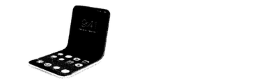
ところで、近年、図24に示すような折り曲げ可能な超薄型ディスプレイ(例えば、有機EL表示装置、液晶表示装置)の開発が進んでいる。超薄型ディスプレイでは、薄型化の実現のために、例えば、カバー材料として従来のカバーガラスに代えて「カバーフィルム」,「ウィンドウフィルム」などと呼ばれる新素材が用いられている。また、円偏光板をカバーフィルムの内部に塗布形式で形成する構成が採用されることもある。
しかしながら、薄型化の進展に伴いタッチ位置の検出精度が低下するという問題が生じている。これについて、以下に説明する。静電容量方式のタッチパネルでは、認識対象物-センサ電極間の距離に応じてセンサ感度が決まる。認識対象物-センサ電極間の距離は、センサ電極上に配置されるカバー材料などの部材の厚みで決まる。カバー材料としてカバーガラスが用いられている構成においては、認識対象物としての指の接触面とセンサ電極との間に適当な間隔がある。このため、相互容量センシングが行われると、或る行に関して例えば図25に示すような検出結果(適切な検出結果)が得られる。これに対して、カバー材料としてカバーフィルムが用いられている構成においては、指の接触面とセンサ電極とが極めて近い距離(例えば0.1mm以下の距離)に位置する。また、カバーフィルムは可撓性を有するため、タッチ時に部材の変形が生じることがある。さらに、タッチ位置に対応するセンサ電極に隣接するセンサ電極(以下「隣接センサ電極」という。)と指とのカップリング(容量結合)の影響が生じることもある。以上のようなことから、相互容量センシングが行われたときに或る行に関して図26に示すような検出結果が得られることがある。図26において、符号91を付した矢印の範囲では、検出結果としての信号値が負の値となっている。本明細書においては、以下、センシングの際に生じるこのような負の値の信号(負値データ)のことを「ネガティブシグナル」という。従来の構成ではこのようなネガティブシグナルの発生を想定していないため、ネガティブシグナルが生じるとタッチ位置を正しく特定することができなくなる。
ここで、隣接センサ電極と指とのカップリングの影響について説明する。図27は、指とセンサ電極との間に充分な間隔がある場合の電気の流れについて説明するための図である。図28は、指とセンサ電極との間の距離が極めて短い場合の電気の流れについて説明するための図である。相互容量センシングに関し、センサ電極は、送信側電極Txと受信側電極Rxとからなる。図27および図28において、送信側電極Tx(93)および受信側電極Rx(93)はタッチ位置に対応するセンサ電極であり、送信側電極Tx(94)および受信側電極Rx(94)は隣接センサ電極である。指とセンサ電極との間に充分な間隔がある場合には、図27で符号92を付した矢印で示すように、タッチ位置に対応する送信側電極Tx(93)から指を介して人体のグラウンドGNDへと電気が流れる。これにより、送信側電極Tx(93)から受信側電極Rx(93)へと流れる電気量と送信側電極Tx(94)から受信側電極Rx(94)へと流れる電気量との間に差が生じる。この差が、検出信号の正の値として現れる。これに対して、指とセンサ電極との間の距離が極めて短い場合には、図28で符号95を付した矢印で示すように、隣接センサ電極としての送信側電極Tx(94)から指を介してタッチ位置に対応する受信側電極Rx(93)にも電気が流れる。これにより、受信側電極Rx(93)へと流れる電気量が大きくなり、上述したネガティブシグナルが現れる。
以上のように、超薄型ディスプレイでは、相互容量センシングの際にネガティブシグナルが生じることがある。ネガティブシグナルが生じると、信号値(検出結果としての信号値)の面内分布が乱れる。タッチ位置は典型的には信号値の面内分布に基づき重心を計算することによって求められるので、信号値の面内分布の乱れがあるとタッチ位置を正しく求めることができない。その結果、タッチ位置の検出精度が悪化する。
そこで、以下の開示は、薄型化が進んでもタッチ位置を精度良く検出することのできる位置検出装置を備えた電子装置を実現することを目的とする。
本開示のいくつかの実施形態に係る電子装置は、画像を表示する表示パネルとタッチ位置の検出を行う位置検出装置とを備えた電子装置であって、
前記位置検出装置は、
前記表示パネルの表面に設けられたタッチパネルと、
タッチ位置の検出が自己容量方式および相互容量方式の双方で行われるよう前記タッチパネルを駆動するタッチパネル駆動回路と、
タッチ位置を、自己容量方式で検出されたデータである自己容量検出データと、相互容量方式で検出されたデータである相互容量検出データとに基づいて特定する位置検出回路と
を含み、
前記位置検出回路は、
前記相互容量検出データに負値データが含まれている場合に、
相互容量方式で負値データが検出された負値データ領域および前記負値データ領域に隣接し相互容量方式で正値データが検出された正値データ領域からなる相互容量検出領域と、自己容量方式で有意なデータが検出された自己容量検出領域とが重なっている領域があれば、
前記自己容量検出データに基づいて前記相互容量検出データを補正する補正処理を実行し、当該補正処理後の相互容量検出データに基づいてタッチ位置を特定する。
前記位置検出装置は、
前記表示パネルの表面に設けられたタッチパネルと、
タッチ位置の検出が自己容量方式および相互容量方式の双方で行われるよう前記タッチパネルを駆動するタッチパネル駆動回路と、
タッチ位置を、自己容量方式で検出されたデータである自己容量検出データと、相互容量方式で検出されたデータである相互容量検出データとに基づいて特定する位置検出回路と
を含み、
前記位置検出回路は、
前記相互容量検出データに負値データが含まれている場合に、
相互容量方式で負値データが検出された負値データ領域および前記負値データ領域に隣接し相互容量方式で正値データが検出された正値データ領域からなる相互容量検出領域と、自己容量方式で有意なデータが検出された自己容量検出領域とが重なっている領域があれば、
前記自己容量検出データに基づいて前記相互容量検出データを補正する補正処理を実行し、当該補正処理後の相互容量検出データに基づいてタッチ位置を特定する。
本開示のいくつかの実施形態に係るタッチ位置検出方法は、タッチ位置の検出を自己容量方式および相互容量方式の双方で行うことができる位置検出装置によるタッチ位置検出方法であって、
相互容量方式で検出されたデータである相互容量検出データに負値データが含まれているか否かを判定する第1判定ステップと、
前記第1判定ステップで前記相互容量検出データに負値データが含まれていると判定された場合に、相互容量方式で負値データが検出された負値データ領域および前記負値データ領域に隣接し相互容量方式で正値データが検出された正値データ領域からなる相互容量検出領域と、自己容量方式で有意なデータが検出された自己容量検出領域とが重なっている領域があるか否かを判定する第2判定ステップと、
前記第2判定ステップで前記相互容量検出領域と前記自己容量検出領域とが重なっている領域があると判定された場合に、前記負値データの絶対値の最大値および前記負値データ領域の面積がそれぞれ予め定められた閾値以上であるか否かを判定する第3判定ステップと、
前記第3判定ステップで前記負値データの絶対値の最大値および前記負値データ領域の面積の双方がそれぞれ予め定められた閾値以上であると判定された場合に、自己容量方式で検出された有意なデータに基づいて前記相互容量検出データを補正する補正ステップと、
前記補正ステップによる補正後の相互容量検出データに基づいてタッチ位置を特定するタッチ位置特定ステップと
を含む。
相互容量方式で検出されたデータである相互容量検出データに負値データが含まれているか否かを判定する第1判定ステップと、
前記第1判定ステップで前記相互容量検出データに負値データが含まれていると判定された場合に、相互容量方式で負値データが検出された負値データ領域および前記負値データ領域に隣接し相互容量方式で正値データが検出された正値データ領域からなる相互容量検出領域と、自己容量方式で有意なデータが検出された自己容量検出領域とが重なっている領域があるか否かを判定する第2判定ステップと、
前記第2判定ステップで前記相互容量検出領域と前記自己容量検出領域とが重なっている領域があると判定された場合に、前記負値データの絶対値の最大値および前記負値データ領域の面積がそれぞれ予め定められた閾値以上であるか否かを判定する第3判定ステップと、
前記第3判定ステップで前記負値データの絶対値の最大値および前記負値データ領域の面積の双方がそれぞれ予め定められた閾値以上であると判定された場合に、自己容量方式で検出された有意なデータに基づいて前記相互容量検出データを補正する補正ステップと、
前記補正ステップによる補正後の相互容量検出データに基づいてタッチ位置を特定するタッチ位置特定ステップと
を含む。
本開示のいくつかの実施形態によれば、相互容量センシング(相互容量方式による位置検出)によって負値データが生じた場合に、所定の条件を満たしていると、自己容量検出データに基づいて相互容量検出データが補正される。そして、補正後の相互容量検出データに基づいてタッチ位置が特定される。指などの認識対象物からタッチパネルまでの距離に関わらず自己容量センシング(自己容量方式による位置検出)によれば安定した検出結果が得られるので、自己容量検出データに基づいて相互容量検出データを補正することによって、補正後の相互容量検出データの値を負値データの影響が除去された好適な値にすることができる。これにより、負値データが生じても精度良くタッチ位置を特定することが可能となる。以上より、薄型化が進んでもタッチ位置を精度良く検出することのできる位置検出装置を備えた電子装置(有機EL表示装置や液晶表示装置など)が実現される。
以下、添付図面を参照しつつ、一実施形態について説明する。なお、以下では、タッチパネルを備えた電子装置として有機EL表示装置を例に挙げて説明する。また、以下において、m、n、M、およびNは2以上の整数であり、iは1以上n以下の整数であり、jは1以上m以下の整数である。また、自己容量センシングによって得られる検出データを「自己容量検出データ」といい、相互容量センシングによって得られる検出データを「相互容量検出データ」という。
<1.有機EL表示装置の構成および動作の概略>
図2は、一実施形態に係る有機EL表示装置10の構成を示すブロック図である。この有機EL表示装置10は、有機ELパネル(表示パネル)11、表示制御回路12、走査線駆動回路13、データ線駆動回路14、電源回路15、タッチパネル20、およびタッチパネルコントローラ30を備えている。
図2は、一実施形態に係る有機EL表示装置10の構成を示すブロック図である。この有機EL表示装置10は、有機ELパネル(表示パネル)11、表示制御回路12、走査線駆動回路13、データ線駆動回路14、電源回路15、タッチパネル20、およびタッチパネルコントローラ30を備えている。
タッチパネル20は、有機ELパネル11の表面に設けられている。タッチパネル20の表面は、「カバーフィルム」,「ウィンドウフィルム」などと呼ばれるフィルム状のカバー素材によって形成されている。また、有機ELパネル11およびタッチパネル20は可撓性を有する。すなわち、本実施形態に係る有機EL表示装置10は、折り曲げることが可能な、タッチパネル付きの超薄型ディスプレイである。
有機ELパネル11は、n本の走査線G1~Gn、m本のデータ線D1~Dm、および(m×n)個の画素回路17を含んでいる。走査線G1~Gnは、互いに平行に配置されている。データ線D1~Dmは、互いに平行に配置されている。走査線G1~Gnとデータ線D1~Dmとは直交している。(m×n)個の画素回路17は、走査線G1~Gnとデータ線D1~Dmとの交点に対応して配置されている。
表示制御回路12は、走査線駆動回路13、データ線駆動回路14、電源回路15、およびタッチパネルコントローラ30に、それぞれ、制御信号CS1、CS2、CS3、およびCS4を出力する。表示制御回路12は、また、この有機EL表示装置10の外部から入力された映像信号DVをデータ線駆動回路14へと出力する。その際、映像信号DVに対して適宜の補正が施されることもある。
走査線駆動回路13は、制御信号CS1に基づき走査線G1~Gnを駆動する。データ線駆動回路14は、制御信号CS2と映像信号DVとに基づきデータ線D1~Dmを駆動する。より詳細には、各ライン期間において、走査線駆動回路13は、n本の走査線G1~Gnの中から1本の走査線を選択し、選択した走査線に選択電圧(画素回路17内の書き込み制御トランジスタがオンする電圧)を印加する。これにより、選択された走査線に接続されたm個の画素回路17が一括して選択される。データ線駆動回路14は、映像信号DVに応じたm個のデータ電圧をデータ線D1~Dmにそれぞれ印加する。これにより、選択されたm個の画素回路にm個のデータ電圧がそれぞれ書き込まれる。なお、走査線駆動回路13は、画素回路17と共に有機ELパネル11内に形成されている。
有機ELパネル11には、(m×n)個の画素回路17に共通のローレベル電源電圧ELVSSを供給するための電極である共通電極(図2では不図示)と、当該(m×n)個の画素回路17にハイレベル電源電圧ELVDDを供給するための電源配線18とが形成されている。電源回路15は、制御信号CS3に基づき、共通電極にローレベル電源電圧ELVSSを印加し、電源配線18にハイレベル電源電圧ELVDDを印加する。
タッチパネルコントローラ30は、タッチパネル駆動回路31と位置検出回路32とを含んでいる。タッチパネルコントローラ30は、タッチパネル20の動作を制御する。その際、タッチパネル駆動回路31は、表示制御回路12から与えられる制御信号CS4に基づき、タッチ位置の検出を行うための駆動信号SDをタッチパネル20に与える。ところで、本実施形態においては、タッチ位置の検出を自己容量方式および相互容量方式の双方で行うことのできる構成が採用されている。すなわち、タッチパネル駆動回路31は、タッチ位置の検出が自己容量方式および相互容量方式の双方で行われるようタッチパネル20を駆動する。タッチパネル20からタッチパネルコントローラ30に検出信号SXが与えられると、当該検出信号SXに基づき、タッチパネル20に対するタッチが行われた位置を位置検出回路32が特定する。詳しくは、検出信号SXから相互容量検出データおよび自己容量検出データが得られ、位置検出回路32は、自己容量検出データと相互容量検出データとに基づいてタッチ位置を特定する(但し、後述するように、タッチ位置の最終的な特定は相互容量検出データのみに基づいて行われる)。そして、タッチパネルコントローラ30は、タッチ位置に応じた処理が行われるよう、表示制御回路12に制御信号(位置信号)PSを与える。
なお、本実施形態においては、タッチパネル20とタッチパネルコントローラ30(タッチパネル駆動回路31および位置検出回路32)とによって位置検出装置が実現されている。
図3は、i行j列目の画素回路17の回路図である。画素回路17は、トランジスタ(駆動トランジスタ)T1、トランジスタ(書き込み制御トランジスタ)T2、容量C1、および有機EL素子L1を含んでいる。有機EL素子L1は、赤、緑、および青のいずれかの色に発光する電気光学素子である。トランジスタT1、T2は、Nチャネル型の薄膜トランジスタ(TFT)である。トランジスタT1、T2としては、酸化物TFT(酸化物半導体をチャネル層に用いた薄膜トランジスタ)やアモルファスシリコンTFTなどを採用することができる。酸化物TFTとしては、例えば、InGaZnO(酸化インジウムガリウム亜鉛)を含むTFTが挙げられる。酸化物TFTを採用することによって、例えば、高精細化や低消費電力化を図ることが可能となる。なお、トランジスタT2については、ゲート端子(制御端子)以外の2つの端子の電位の高低関係が状態によって入れ替わる。従って、トランジスタT2については、ゲート端子以外の2つの端子のうちの一方を「第1導通端子」といい、他方を「第2導通端子」という。
トランジスタT1のゲート端子、トランジスタT2の第2導通端子、および容量C1の一端は互いに接続されている。なお、これらが互いに接続されている領域(配線)のことを「制御ノード」という。制御ノードには符号Naを付す。トランジスタT1については、ゲート端子は制御ノードNaに接続され、ドレイン端子はハイレベル電源電圧ELVDDが印加された電源配線18に接続され、ソース端子は有機EL素子L1のアノード端子に接続されている。トランジスタT2については、ゲート端子は走査線Giに接続され、第1導通端子はデータ線Djに接続され、第2導通端子は制御ノードNaに接続されている。容量C1については、一端は制御ノードNaに接続され、他端はトランジスタT1のドレイン端子に接続されている。有機EL素子L1については、アノード端子はトランジスタT1のソース端子に接続され、カソード端子はローレベル電源電圧ELVSSが印加された共通電極19に接続されている。
走査線Giの電圧がハイレベルになると、トランジスタT2はオン状態となり、制御ノードNaにはデータ線Djの電圧が印加される。走査線Giの電圧がローレベルになると、トランジスタT2はオフ状態となる。トランジスタT2がオフ状態になると、制御ノードNaはフローティング状態になり、容量C1にはトランジスタT1のゲート-ドレイン間電圧が保持される。トランジスタT1と有機EL素子L1とを流れる駆動電流は、トランジスタT1のゲート-ソース間電圧に応じて変化する。有機EL素子L1は、駆動電流の大きさに応じた輝度で発光する。このようにして各画素回路17内の有機EL素子L1が発光することによって、有機ELパネル11に画像が表示される。
なお、図3に示した画素回路17の構成は一例であって、様々な構成の画素回路を採用することができる。
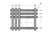
図4は、タッチパネル20の平面図の一例である。図4に示すタッチパネル20は、センサ電極として、N本のドライブ線(送信側電極)Tx1~TxNとM本のセンス線(受信側電極)Rx1~RxMとを含んでいる。ドライブ線Tx1~TxNは、互いに平行に配置されている。センス線Rx1~RxMは、互いに平行に配置されている。ドライブ線Tx1~TxNとセンス線Rx1~RxMとは直交している。自己容量センシングが行われる際には、全てのドライブ線Tx1~TxNおよび全てのセンス線Rx1~RxMが一斉に駆動される。相互容量センシングが行われる際には、全てのセンス線Rx1~RxMがオンにされた状態でN本のドライブ線Tx1~TxNが1本ずつ駆動される。
なお、タッチパネル20は図5に示すようなダイヤモンドパターンと呼ばれるセンサ電極によって構成されていても良い。この場合、送信側電極Txと受信側電極Rxとを異なる層に形成する構成、送信側電極Txと受信側電極Rxとを同じ層に形成する構成、メタルメッシュタイプと呼ばれる構成(従来のようなITO膜を用いるのではなく銀や銅を用いる構成)などを採用することができる。
<2.タッチ位置の検出方法>
<2.1 概要>
本実施形態においては、タッチ位置の検出が自己容量方式および相互容量方式の双方で行うことが可能となっている。上述したように、相互容量センシングの際にはネガティブシグナル(負値データ)が生じ得る。これに対して、自己容量センシングの際には、ネガティブシグナルは発生しない。そこで、相互容量センシングによってネガティブシグナルが発生した場合には自己容量検出データを用いて相互容量検出データを補正する。そして、補正後の相互容量検出データ(補正が不要な場合は元の相互容量検出データ)に基づいて重心計算を行うことによってタッチ位置の最終的な特定を行う。なお、相互容量センシングについても自己容量センシングについても検出データにはノイズ等が含まれる。そこで、一般に、ノイズ等を除去するための閾値が予め設定されており、当該閾値未満のデータを無視して処理が行われる。すなわち、値が当該閾値以上である検出データ(自己容量検出データ、相互容量検出データ)は有意なデータ(タッチ位置の特定に利用されるデータ)として扱われ、値が当該閾値未満である検出データは非有意なデータ(タッチ位置の特定に利用されないデータ)として扱われる。また、検出データに関して、当該閾値以上の値が有意な値として扱われ、当該閾値未満の値は非有意な値として扱われる。
<2.1 概要>
本実施形態においては、タッチ位置の検出が自己容量方式および相互容量方式の双方で行うことが可能となっている。上述したように、相互容量センシングの際にはネガティブシグナル(負値データ)が生じ得る。これに対して、自己容量センシングの際には、ネガティブシグナルは発生しない。そこで、相互容量センシングによってネガティブシグナルが発生した場合には自己容量検出データを用いて相互容量検出データを補正する。そして、補正後の相互容量検出データ(補正が不要な場合は元の相互容量検出データ)に基づいて重心計算を行うことによってタッチ位置の最終的な特定を行う。なお、相互容量センシングについても自己容量センシングについても検出データにはノイズ等が含まれる。そこで、一般に、ノイズ等を除去するための閾値が予め設定されており、当該閾値未満のデータを無視して処理が行われる。すなわち、値が当該閾値以上である検出データ(自己容量検出データ、相互容量検出データ)は有意なデータ(タッチ位置の特定に利用されるデータ)として扱われ、値が当該閾値未満である検出データは非有意なデータ(タッチ位置の特定に利用されないデータ)として扱われる。また、検出データに関して、当該閾値以上の値が有意な値として扱われ、当該閾値未満の値は非有意な値として扱われる。
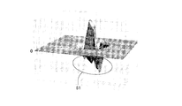
ここで、以下の説明で用いる用語について説明する。図6は、相互容量センシングの検出結果を3次元状に表した図(以下、このような図を「3次元マップ」という。)である。図6において符号51を付した部分は、ネガティブシグナルが生じていることを表している。このようなネガティブシグナルが生じている領域のことを「負値データ領域」という。また、相互容量センシングの検出結果として正の値(正値データ)が得られている領域のことを「正値データ領域」という。負値データ領域と正値データ領域とからなる領域を「相互容量検出領域」という。
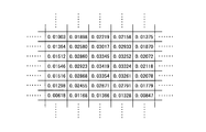
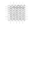
自己容量センシングの検出結果は、ドライブ線毎およびセンス線毎に得られる。すなわち、検出結果としての信号値は、X軸方向の座標毎に得られるとともにY軸方向の座標毎に得られる。ここで、X軸方向の各座標の信号値に対してX軸方向の全座標の信号値の合計を1とする正規化を施し、Y軸方向の各座標の信号値に対してY軸方向の全座標の信号値の合計を1とする正規化を施す。X軸方向の各座標の正規化後の信号値とY軸方向の各座標の正規化後の信号値とを乗ずることによって、自己容量センシングに基づく3次元データが生成される。この3次元データの一部の一例を図7に示している。また、3次元データに基づく3次元マップの一例を図8に示している。上記のようにして得られた3次元データの値を閾値と比較して、閾値以上の値のデータを有意なデータと判断する。自己容量センシングによってこのような有意なデータが得られた領域を「自己容量検出領域」という。図9に示すように、X軸方向に関して符号52を付した部分のような信号値が得られていて、かつ、Y軸方向に関して符号53を付した部分のような信号値が得られている場合に、例えば符号54を付した極太線内の領域が自己容量検出領域となる。
なお、上述のような自己容量検出領域は位置検出回路32によって定められる。また、例えば、X軸方向が第1軸方向に相当し、Y軸方向が第2軸方向に相当する。また、3次元データの値との比較対象となる閾値が第4の閾値に相当する。
図10は、自己容量検出領域と負値データ領域と正値データ領域との重なり方の一例を示す図である。符号56を付した太線内の領域が正値データ領域である。符号55を付した太線内の領域のうち正値データ領域(符号56を付した太線内の領域)を除いた領域が負値データ領域である。相互容量検出領域は負値データ領域と正値データ領域とからなる領域であるので、符号55を付した太線内の領域が相互容量検出領域である。
<2.2 位置検出のための処理の概略手順>
図11に示すフローチャートを参照しつつ、位置検出のための処理の概略手順について説明する。なお、有機EL表示装置10の動作中、図11に示すステップS10~S70の処理が繰り返し行われる。
図11に示すフローチャートを参照しつつ、位置検出のための処理の概略手順について説明する。なお、有機EL表示装置10の動作中、図11に示すステップS10~S70の処理が繰り返し行われる。
まず、タッチパネル駆動回路31が相互容量センシング用の駆動信号SDをタッチパネル20に与える(ステップS10)。そして、位置検出回路32が検出信号SXを受け取る(ステップS20)。次に、タッチパネル駆動回路31が再び相互容量センシング用の駆動信号SDをタッチパネル20に与える(ステップS30)。そして、位置検出回路32が検出信号SXを受け取る(ステップS40)。なお、ステップS10とステップS30とで駆動信号SDの位相は異なる。これにより、ペアとなる2つの列に着目したときに、ステップS20では一方の列についての検出データが得られ、ステップS40では他方の列についての検出データが得られる。その後、タッチパネル駆動回路31が自己容量センシング用の駆動信号SDをタッチパネル20に与える(ステップS50)。そして、位置検出回路32が検出信号SXを受け取る(ステップS60)。最後に、位置検出回路32が、ステップS20、ステップS40、およびステップS60で取得した検出信号SXに基づいて、位置特定処理(タッチの有無を判定してタッチがされている場合にはタッチ位置を特定する処理)を行う(ステップS70)。
<2.3 位置特定処理>
<2.3.1 処理手順>
次に、図1に示すフローチャートを参照しつつ、位置特定処理(図11のステップS70の処理)について詳しく説明する。この位置特定処理は、タッチパネルコントローラ30内の位置検出回路32で行われる。
<2.3.1 処理手順>
次に、図1に示すフローチャートを参照しつつ、位置特定処理(図11のステップS70の処理)について詳しく説明する。この位置特定処理は、タッチパネルコントローラ30内の位置検出回路32で行われる。
位置特定処理の開始後、まず、タッチ信号が検出されたか否かの判定が行われる(ステップS700)。なお、ここでのタッチ信号は、検出信号SXについての有意な変化を意味する。ステップS700での判定の結果、タッチ信号が検出された場合には処理はステップS710に進み、タッチ信号が検出されなかった場合にはこの位置特定処理は終了する。
ステップS710では、相互容量検出データにネガティブシグナル(負値データ)が含まれているか否かの判定が行われる。その結果、相互容量検出データにネガティブシグナルは含まれていないと判定された場合には処理はステップS715に進み、相互容量検出データにネガティブシグナルが含まれていると判定された場合には処理はステップS720に進む。
ステップS715では、相互容量検出データの値をそのまま用いて重心計算を行うことによってタッチ位置が算出(特定)される。
ステップS720では、相互容量検出領域と自己容量検出領域とが重なっている領域があるか否かの判定が行われる。換言すれば、相互容量検出領域内に自己容量検出データとして有意なデータが検出された領域があるか否かの判定が行われる。その結果、相互容量検出領域と自己容量検出領域とが重なっている領域があると判定された場合には、処理はステップS730に進む。一方、相互容量検出領域と自己容量検出領域とが重なっている領域がないと判定された場合には、タッチ信号は水滴に起因して検出されたとみなして、タッチ位置を特定することなくこの位置特定処理は終了する。
ステップS730では、補正処理が必要であるか否かの判定が行われる。具体的には、ネガティブシグナルの絶対値の最大値および負値データ領域の大きさ(面積)がそれぞれ予め定められた閾値以上であるか否かの判定が行われ、ネガティブシグナルの絶対値の最大値および負値データ領域の大きさ(面積)の双方がそれぞれ予め定められた閾値以上であれば補正処理が必要であると判定される。ステップS730での判定の結果、補正処理が必要であると判定された場合には処理はステップS740に進み、補正処理が必要ではないと判定された場合には処理はステップS735に進む。なお、ネガティブシグナルの絶対値の最大値との比較対象となる閾値が第2の閾値に相当し、負値データ領域の大きさ(面積)との比較対象となる閾値が第3の閾値に相当する。
ステップS735では、相互容量検出データの値をそのまま用いて重心計算を行うことによってタッチ位置が算出(特定)される。すなわち、正値データ領域についての相互容量検出データの値および負値データ領域についての相互容量検出データの値をそのまま用いてタッチ位置が算出される。なお、相互容量検出データに対して後述する第1の補正処理と同様の補正処理を施して補正後の相互容量検出データを用いてタッチ位置を算出するようにしても良い。
ステップS740では、ネガティブシグナルによる影響が除去されるよう、自己容量検出データに基づき相互容量検出データを補正する補正処理が行われる。なお、補正処理の詳しい説明については後述する。ステップS750では、ステップS740での補正処理で得られた補正後の相互容量検出データを用いて重心計算を行うことによってタッチ位置が算出(特定)される。
ステップS760では、ステップS715、ステップS735、およびステップS750のいずれかで特定されたタッチ位置の出力(特定されたタッチ位置を示す制御信号PSの出力)が行われる。これにより、位置特定処理は終了する。
以上のように、位置検出回路32は、相互容量検出データにネガティブシグナル(負値データ)が含まれている場合に、相互容量センシングでネガティブシグナル(負値データ)が検出された負値データ領域および当該負値データ領域に隣接し相互容量センシングで正値データが検出された正値データ領域からなる相互容量検出領域と、自己容量センシングで有意なデータが検出された自己容量検出領域とが重なっている領域があれば(但し、ネガティブシグナルの絶対値の最大値および負値データ領域の大きさが閾値以上の場合)、自己容量検出データに基づいて相互容量検出データを補正する補正処理を実行し、当該補正処理後の相互容量検出データに基づいてタッチ位置を特定する。相互容量検出データに正値データのみが含まれている場合には、位置検出回路32は、自己容量検出データを用いずに、相互容量検出データのみに基づいてタッチ位置を特定する。
なお、本実施形態においては、ステップS710によって第1判定ステップが実現され、ステップS720によって第2判定ステップが実現され、ステップS730によって第3判定ステップが実現され、ステップS740によって補正ステップが実現され、ステップS750によってタッチ位置特定ステップが実現されている。
<2.3.2 補正処理>
次に、補正処理について詳しく説明する。本実施形態においては、図1のステップS740の補正処理に関して2つの補正手法が用意される。このように2つの補正手法が用意される理由は、ネガティブシグナルが生じたときに後述するシグナル崩壊が起こった場合とシグナル崩壊が起こらなかった場合とでは補正前の相互容量検出データがかなり異なり、両者を一律に扱うことができないからである。
次に、補正処理について詳しく説明する。本実施形態においては、図1のステップS740の補正処理に関して2つの補正手法が用意される。このように2つの補正手法が用意される理由は、ネガティブシグナルが生じたときに後述するシグナル崩壊が起こった場合とシグナル崩壊が起こらなかった場合とでは補正前の相互容量検出データがかなり異なり、両者を一律に扱うことができないからである。
静電容量方式のタッチパネルで得られる検出信号は、人体を導体とみなしたときのグラウンド電位とタッチパネルのグラウンド電位とが共通するか否かによって変化する。また、当該検出信号は、ターゲットサイズ(認識対象物のタッチ面積)によっても変化する。これに関し、人体を導体とみなしたときのグラウンド電位とタッチパネルのグラウンド電位とが共通ではない状態(フローティング状態)のとき(例えば、スマートフォンのようにタッチパネル付き電子装置がAC電源に接続されていないとき)にはタッチパネルから人体へと静電気は流れにくく、このようなフローティング状態のときに大きな指でタッチがなされると、本来とは異なる電気の流れが生じる。その結果、相互容量センシングによって、その3次元マップが例えば図12のように表される相互容量検出データが得られる。図12に示す例では、タッチ位置の中心部のデータが、タッチ位置の特定に不適切なデータ(以下、単に「不適切データ」という。)となっている。このような状態のことを「シグナル崩壊」という。
図6に示した例のようにネガティブシグナルは生じているがシグナル崩壊は生じていない場合には、タッチ位置の中心部のデータが不適切データではないため、ネガティブシグナルを無視する、すなわち、負値データ領域についての相互容量検出データの値を例えば0に補正することによって、ネガティブシグナルの影響を除去することができると考えられる。これに対して、図12に示した例のようにネガティブシグナルが生じていてシグナル崩壊も生じている場合には、タッチ位置の中心部のデータが不適切データであるため、負値データ領域についての相互容量検出データの値を0に補正するだけではタッチ位置を精度良く求めることはできない。従って、上述したように2つの補正手法が用意される。これに関し、シグナル崩壊はターゲットサイズが大きいときに生じるので、ターゲットサイズの大小に基づいて補正手法を決定するのが好ましい。ところで、ターゲットサイズの大小は、自己容量センシングの検出結果から判断することができる。これについて、以下に説明する。
自己容量センシングでは、1つのセンサ電極における容量値の差分の検出が行われるので、隣接センサ電極の状態が検出信号の値(信号レベル)に影響を及ぼすことはない。従って、認識対象物としての指の接触面とセンサ電極との距離に関わらず、ネガティブシグナルは生じない。また、フローティング状態であることが検出信号の値に及ぼす影響は小さい。このように、自己容量センシングによれば、安定した検出結果が得られる。図13は、自己容量センシングで得られた信号レベル(X軸方向についての信号レベル)のターゲットサイズによる違いを示すグラフである。符号61a、61b、61c、61d、61e、および61fを付した折れ線は、それぞれ、ターゲットサイズ(直径)が4mm、8mm、12mm、16mm、20mm、および30mmのデータを表している。図14は、図13に基づく「ターゲットサイズと信号レベルとの関係」を表すグラフである。図15は、自己容量センシングで得られた信号レベル(Y軸方向についての信号レベル)のターゲットサイズによる違いを示すグラフである。符号62a、62b、62c、62d、62e、および62fを付した折れ線は、それぞれ、ターゲットサイズ(直径)が4mm、8mm、12mm、16mm、20mm、および30mmのデータを表している。図16は、図15に基づく「ターゲットサイズと信号レベルとの関係」を表すグラフである。図13~図16より、ターゲットサイズが大きくなるについて信号レベルも大きくなることが把握される。すなわち、信号レベルに基づいてターゲットサイズの大小を判断することができる。以上のように、自己容量センシングの検出結果からターゲットサイズの大小を判断することができる。
そこで、本実施形態においては、自己容量センシングの検出結果に応じて2つの補正手法を切り替えつつ、相互容量検出データの値を補正する補正処理が行われる。以下、図17に示すフローチャートを参照しつつ、補正処理の詳細な手順について説明する。
補正処理の開始後、まず、相互容量検出領域における自己容量検出データの最大値(以下「自己容量最大値」という。)の特定が行われる(ステップS741)。自己容量センシングの際にはドライブ線毎およびセンス線毎に検出信号SXが得られるので、ステップS741では、自己容量最大値として、ドライブ線についての最大値(以下「第1軸最大値」という。)とセンス線についての最大値(以下「第2軸最大値」という。)とが得られる。
次に、補正手法を決定するための補正ランクが自己容量最大値に基づいて判定される(ステップS742)。本実施形態においては、「大」および「小」という2つの補正ランクが用意されている。補正ランク「大」はターゲットサイズが大きい場合の補正手法に対応付けられ、補正ランク「小」はターゲットサイズが小さい場合の補正手法に対応付けられる。ステップS742では、第1軸最大値および第2軸最大値が予め用意された閾値と比較される。第1軸最大値が閾値以下であって、かつ、第2軸最大値が閾値以下である場合には、ターゲットサイズは小さいと考えられるので、補正ランクは「小」と判定される。第1軸最大値が閾値よりも大きい又は第2軸最大値が閾値よりも大きい場合には、ターゲットサイズは大きいと考えられるので、補正ランクは「大」と判定される。補正ランクは「小」であると判定された場合には処理はステップS743に進み、補正ランクは「大」であると判定された場合には処理はステップS744に進む。
なお、自己容量検出領域の面積を閾値と比較することによって補正ランクを決定するようにしても良い。また、自己容量検出データに基づいて求められる重心位置における値と自己容量検出領域の面積とに基づいて補正ランクを決定するようにしても良い。さらに、ここでは2つの補正手法を用意する例を示しているが、3つ以上の補正手法を用意しておいて多段階の閾値を設けてターゲットサイズに応じて適宜の補正手法により補正が行われるようにしても良い。
ステップS743では、補正ランク「小」に対応する補正処理である第1の補正処理が行われる。第1の補正処理は、ターゲットサイズが小さい場合に対応付けられた処理であって、典型的には、シグナル崩壊が生じていない場合や仮にシグナル崩壊が生じていてもその範囲が極めて狭いような場合に行われる。第1の補正処理では、負値データ領域についての相互容量検出データの値が0以上の所定値(固定値)に補正される。好ましくは、その所定値は、有意な検出信号が得られなかったものとして処理されるよう、所定の閾値以下の値(例えば「0」)とされる。すなわち、相互容量検出データの値として非有意な値を上記所定値に定めることが好ましい。第1の補正処理によって、相互容量検出データに基づく3次元マップは、例えば、図18に示すようなものから図19に示すようなものへと変化する。
ステップS744では、補正ランク「大」に対応する補正処理である第2の補正処理が行われる。第2の補正処理は、ターゲットサイズが大きい場合に対応付けられた処理であって、典型的には、シグナル崩壊が広い範囲で生じている場合に行われる。第2の補正処理では、自己容量検出データを用いて、相互容量検出データに対して補正後の3次元マップが山型の形状となるように補正が施される。具体的には、まず、相互容量検出データの全ての値が「0」に書き換えられる。そして、自己容量検出データの最大値が相互容量検出データの取り得る最大値(例えば、相互容量検出データが10ビットのデータであれば“1024”)に等しい値となるよう、自己容量検出データの全ての値に対して正規化が施される。例えば、図7に示したデータが正規化によって図20に示すようなデータとなる。さらに、相互容量検出データの各値が、正規化後の自己容量検出データのうちの対応する位置の値に書き換えられる。これにより、相互容量検出領域と自己容量検出領域とは等しくなる。
第2の補正処理の実行前に自己容量検出領域と負値データ領域と正値データ領域との重なり方が図10に示すようなものである場合、第2の補正処理によって、図21に関し「符号71を付した領域の信号値>符号72を付した領域の信号値>符号73を付した領域の信号値」という関係を満たすように相互容量検出データの値が補正される。第2の補正処理によって、相互容量検出データに基づく3次元マップは、例えば、図12に示すようなものから図22に示すようなものへと変化する。
以上のように、本実施形態では、2つの補正手法の組み合わせとして、負値データ領域についての相互容量検出データの値を0以上の所定値に補正するという手法(第1の補正処理)と、負値データ領域を含んでいる相互容量検出領域についての自己容量検出データの最大値が相互容量検出データの取り得る最大値に等しい値となるよう自己容量検出データに正規化を施した上で相互容量検出データの各値を正規化後の自己容量検出データのうちの対応する位置の値に補正するという手法(第2の補正処理)との組み合わせが採用されている。
<2.3.3 第2の補正処理の変形例>
ここで、第2の補正処理の変形例について説明する。本変形例では、自己容量検出データを用いて、相互容量検出データに対して補正後の3次元マップが四角錐台に近い形状となるように補正が施される。具体的には、まず、自己容量検出領域以外の領域についての相互容量検出データの値が予め定められた閾値(この閾値が第1の閾値に相当する)以下の値に書き換えられる。好ましくは、自己容量検出領域以外の領域についての相互容量検出データの値は、有意な検出信号が得られなかったものとして処理されるよう例えば「0」に書き換えられる。そして、自己容量検出領域についての相互容量検出データの値が上記閾値値以上の所定値(固定値)に補正される。なお、相互容量検出データの値に関して有意な値と非有意な値との境界となる値が上記閾値に定められるのが好ましい。また、例えば、上記所定値は、相互容量検出データの取り得る最大値(例えば、相互容量検出データが10ビットのデータであれば“1024”)に等しい値に定められる。なお、補正後の3次元マップの形状が直方体ではなく四角錐台に近い形状となる理由は、値(3次元データの値)が変化する境界部分において境界の一方の側の領域の値を表す座標(3次元空間上の座標)と境界の他方の側の領域の値を表す座標(3次元空間上の座標)とを結ぶ線が値を0とする平面に対して垂直になるのではないからである。
ここで、第2の補正処理の変形例について説明する。本変形例では、自己容量検出データを用いて、相互容量検出データに対して補正後の3次元マップが四角錐台に近い形状となるように補正が施される。具体的には、まず、自己容量検出領域以外の領域についての相互容量検出データの値が予め定められた閾値(この閾値が第1の閾値に相当する)以下の値に書き換えられる。好ましくは、自己容量検出領域以外の領域についての相互容量検出データの値は、有意な検出信号が得られなかったものとして処理されるよう例えば「0」に書き換えられる。そして、自己容量検出領域についての相互容量検出データの値が上記閾値値以上の所定値(固定値)に補正される。なお、相互容量検出データの値に関して有意な値と非有意な値との境界となる値が上記閾値に定められるのが好ましい。また、例えば、上記所定値は、相互容量検出データの取り得る最大値(例えば、相互容量検出データが10ビットのデータであれば“1024”)に等しい値に定められる。なお、補正後の3次元マップの形状が直方体ではなく四角錐台に近い形状となる理由は、値(3次元データの値)が変化する境界部分において境界の一方の側の領域の値を表す座標(3次元空間上の座標)と境界の他方の側の領域の値を表す座標(3次元空間上の座標)とを結ぶ線が値を0とする平面に対して垂直になるのではないからである。
本変形例によれば、第2の補正処理の実行前に自己容量検出領域と負値データ領域と正値データ領域との重なり方が図10に示すようなものである場合、第2の補正処理によって、図9で符号54を付した極太線内の領域については値が閾値以上の所定値(固定値)となり、かつ、それ以外の領域については値が例えば「0」となるように、相互容量検出データの値が補正される。従って、本変形例においては、相互容量検出データに基づく3次元マップは、例えば、図12に示すようなものから図23に示すようなものへと変化する。
本変形例においては、2つの補正手法の組み合わせとして、負値データ領域についての相互容量検出データの値を0以上の所定値に補正するという手法(第1の補正処理)と、負値データ領域を含んでいる相互容量検出領域のうち自己容量検出領域とは重なっていない領域についての相互容量検出データの値を予め定められた閾値(第1の閾値)以下の値に書き換えた上で負値データ領域を含んでいる相互容量検出領域のうち自己容量検出領域と重なっている領域についての相互容量検出データの値を上記閾値(第1の閾値)以上の所定値に補正するという手法(第2の補正処理)との組み合わせが採用されている。
<3.効果>
本実施形態によれば、相互容量センシングによってネガティブシグナルが生じた場合に、所定の条件を満たしていると、自己容量検出データに基づいて相互容量検出データが補正され、補正後の相互容量検出データに基づいてタッチ位置が特定される。指などの認識対象物とセンサ電極間の距離に関わらず自己容量センシングによれば安定した検出結果が得られるので、自己容量検出データに基づいて相互容量検出データを補正することによって、補正後の相互容量検出データの値をネガティブシグナルの影響が除去された好適な値にすることができる。これにより、ネガティブシグナルが生じても精度良くタッチ位置を特定することが可能となる。以上より、本実施形態によれば、薄型化が進んでもタッチ位置を精度良く検出することのできる位置検出装置を備えた有機EL表示装置10が実現される。
本実施形態によれば、相互容量センシングによってネガティブシグナルが生じた場合に、所定の条件を満たしていると、自己容量検出データに基づいて相互容量検出データが補正され、補正後の相互容量検出データに基づいてタッチ位置が特定される。指などの認識対象物とセンサ電極間の距離に関わらず自己容量センシングによれば安定した検出結果が得られるので、自己容量検出データに基づいて相互容量検出データを補正することによって、補正後の相互容量検出データの値をネガティブシグナルの影響が除去された好適な値にすることができる。これにより、ネガティブシグナルが生じても精度良くタッチ位置を特定することが可能となる。以上より、本実施形態によれば、薄型化が進んでもタッチ位置を精度良く検出することのできる位置検出装置を備えた有機EL表示装置10が実現される。
<4.その他>
上記実施形態では位置検出装置を備えた電子装置として有機EL表示装置を例に挙げて説明したが、これには限定されない。タッチパネルを含む位置検出装置を備えたものであれば、液晶表示装置、無機EL表示装置、QLED表示装置、フレキシブル表示装置などにも本発明を適用することができる。
上記実施形態では位置検出装置を備えた電子装置として有機EL表示装置を例に挙げて説明したが、これには限定されない。タッチパネルを含む位置検出装置を備えたものであれば、液晶表示装置、無機EL表示装置、QLED表示装置、フレキシブル表示装置などにも本発明を適用することができる。
10…有機EL表示装置
17…画素回路
20…タッチパネル
30…タッチパネルコントローラ
31…タッチパネル駆動回路
32…位置検出回路
L1…有機EL素子
17…画素回路
20…タッチパネル
30…タッチパネルコントローラ
31…タッチパネル駆動回路
32…位置検出回路
L1…有機EL素子
Claims (16)
- 画像を表示する表示パネルとタッチ位置の検出を行う位置検出装置とを備えた電子装置であって、
前記位置検出装置は、
前記表示パネルの表面に設けられたタッチパネルと、
タッチ位置の検出が自己容量方式および相互容量方式の双方で行われるよう前記タッチパネルを駆動するタッチパネル駆動回路と、
タッチ位置を、自己容量方式で検出されたデータである自己容量検出データと、相互容量方式で検出されたデータである相互容量検出データとに基づいて特定する位置検出回路と
を含み、
前記位置検出回路は、
前記相互容量検出データに負値データが含まれている場合に、
相互容量方式で負値データが検出された負値データ領域および前記負値データ領域に隣接し相互容量方式で正値データが検出された正値データ領域からなる相互容量検出領域と、自己容量方式で有意なデータが検出された自己容量検出領域とが重なっている領域があれば、
前記自己容量検出データに基づいて前記相互容量検出データを補正する補正処理を実行し、当該補正処理後の相互容量検出データに基づいてタッチ位置を特定することを特徴とする、電子装置。 - 前記位置検出回路は、前記補正処理の手法として、前記負値データ領域を含んでいる相互容量検出領域についての前記自己容量検出データの最大値が前記相互容量検出データの取り得る最大値に等しい値となるよう前記自己容量検出データに正規化を施し、前記相互容量検出データの各値を正規化後の自己容量検出データのうちの対応する位置の値に補正することを特徴とする、請求項1に記載の電子装置。
- 前記位置検出回路は、前記補正処理の手法として、前記負値データ領域を含んでいる相互容量検出領域のうち前記自己容量検出領域とは重なっていない領域についての前記相互容量検出データの値を予め定められた第1の閾値以下の値に補正し、前記負値データ領域を含んでいる相互容量検出領域のうち前記自己容量検出領域と重なっている領域についての前記相互容量検出データの値を前記第1の閾値以上の所定値に補正することを特徴とする、請求項1に記載の電子装置。
- 前記第1の閾値は、前記相互容量検出データの値に関して有意な値と非有意な値との境界となる値であることを特徴とする、請求項3に記載の電子装置。
- 前記所定値は、前記相互容量検出データの取り得る最大値に等しい値であることを特徴とする、請求項3に記載の電子装置。
- 前記位置検出回路は、前記補正処理の手法として、前記負値データ領域についての前記相互容量検出データの値を0以上の所定値に補正することを特徴とする、請求項1に記載の電子装置。
- 前記所定値は、前記相互容量検出データの値として非有意な値であることを特徴とする、請求項6に記載の電子装置。
- 前記位置検出回路は、前記相互容量検出データに含まれる負値データの絶対値の最大値が予め定められた第2の閾値以上であって、かつ、前記負値データ領域の面積が予め定められた第3の閾値以上である場合に、前記補正処理を実行することを特徴とする、請求項1に記載の電子装置。
- 前記補正処理の手法として2つ以上の手法が予め用意され、
前記位置検出回路は、前記相互容量検出領域と前記自己容量検出領域とが重なっている領域についての前記自己容量検出データの最大値に基づいて、実行する補正処理の手法を決定する方法を決定することを特徴とする、請求項1に記載の電子装置。 - 前記補正処理の手法として2つ以上の手法が予め用意され、
前記位置検出回路は、前記自己容量検出領域の面積に基づいて、実行する補正処理の手法を決定する方法を決定することを特徴とする、請求項1に記載の電子装置。 - 前記補正処理の手法として2つ以上の手法が予め用意され、
前記位置検出回路は、前記自己容量検出データに基づいて求められる重心位置における値と前記自己容量検出領域の面積とに基づいて、実行する補正処理の手法を決定する方法を決定することを特徴とする、請求項1に記載の電子装置。 - 前記位置検出回路は、前記相互容量検出データに負値データが含まれていて、かつ、前記相互容量検出領域と前記自己容量検出領域とが重なっている領域がなければ、タッチが行われていないと判断してタッチ位置の特定を行わないことを特徴とする、請求項1に記載の電子装置。
- 前記位置検出回路は、自己容量方式によって第1軸方向の座標毎に得られる値であって前記第1軸方向の全ての座標についての値の総和に基づく正規化によって得られる値と自己容量方式によって第2軸方向の座標毎に得られる値であって前記第2軸方向の全ての座標についての値の総和に基づく正規化によって得られる値とを乗ずることによって得られる値が予め定められた第4の閾値以上の値である領域を前記自己容量検出領域に定めることを特徴とする、請求項1に記載の電子装置。
- 前記タッチパネルの表面は、フィルム状のカバー素材によって形成されていることを特徴とする、請求項1に記載の電子装置。
- 前記表示パネルおよび前記タッチパネルは、可撓性を有することを特徴とする、請求項1に記載の電子装置。
- タッチ位置の検出を自己容量方式および相互容量方式の双方で行うことができる位置検出装置によるタッチ位置検出方法であって、
相互容量方式で検出されたデータである相互容量検出データに負値データが含まれているか否かを判定する第1判定ステップと、
前記第1判定ステップで前記相互容量検出データに負値データが含まれていると判定された場合に、相互容量方式で負値データが検出された負値データ領域および前記負値データ領域に隣接し相互容量方式で正値データが検出された正値データ領域からなる相互容量検出領域と、自己容量方式で有意なデータが検出された自己容量検出領域とが重なっている領域があるか否かを判定する第2判定ステップと、
前記第2判定ステップで前記相互容量検出領域と前記自己容量検出領域とが重なっている領域があると判定された場合に、前記負値データの絶対値の最大値および前記負値データ領域の面積がそれぞれ予め定められた閾値以上であるか否かを判定する第3判定ステップと、
前記第3判定ステップで前記負値データの絶対値の最大値および前記負値データ領域の面積の双方がそれぞれ予め定められた閾値以上であると判定された場合に、自己容量方式で検出された有意なデータに基づいて前記相互容量検出データを補正する補正ステップと、
前記補正ステップによる補正後の相互容量検出データに基づいてタッチ位置を特定するタッチ位置特定ステップと
を含むことを特徴とする、タッチ位置検出方法。
Priority Applications (2)
| Application Number | Priority Date | Filing Date | Title |
|---|---|---|---|
| PCT/JP2019/000878 WO2020148798A1 (ja) | 2019-01-15 | 2019-01-15 | 位置検出装置を備えた電子装置およびタッチ位置検出方法 |
| US17/298,753 US11429227B2 (en) | 2019-01-15 | 2019-01-15 | Electronic device provided with position detector and touch position detection method |
Applications Claiming Priority (1)
| Application Number | Priority Date | Filing Date | Title |
|---|---|---|---|
| PCT/JP2019/000878 WO2020148798A1 (ja) | 2019-01-15 | 2019-01-15 | 位置検出装置を備えた電子装置およびタッチ位置検出方法 |
Publications (1)
| Publication Number | Publication Date |
|---|---|
| WO2020148798A1 true WO2020148798A1 (ja) | 2020-07-23 |
Family
ID=71613721
Family Applications (1)
| Application Number | Title | Priority Date | Filing Date |
|---|---|---|---|
| PCT/JP2019/000878 Ceased WO2020148798A1 (ja) | 2019-01-15 | 2019-01-15 | 位置検出装置を備えた電子装置およびタッチ位置検出方法 |
Country Status (2)
| Country | Link |
|---|---|
| US (1) | US11429227B2 (ja) |
| WO (1) | WO2020148798A1 (ja) |
Citations (5)
| Publication number | Priority date | Publication date | Assignee | Title |
|---|---|---|---|---|
| JP2015191550A (ja) * | 2014-03-28 | 2015-11-02 | 株式会社アスコ | 誤検出防止方法、制御プログラム、記録媒体およびタッチパネル装置 |
| JP2017174352A (ja) * | 2016-03-25 | 2017-09-28 | 株式会社ジャパンディスプレイ | 検出装置及びタッチ検出機能付き表示装置 |
| JP2017187946A (ja) * | 2016-04-06 | 2017-10-12 | 富士通株式会社 | 電子機器及び接触検知プログラム |
| US20180011596A1 (en) * | 2016-07-11 | 2018-01-11 | Stmicroelectronics Asia Pacific Pte Ltd | Water rejection for capacitive touch screen |
| US10146390B1 (en) * | 2017-07-21 | 2018-12-04 | Cypress Semiconductor Corporation | Method of combining self and mutual capacitance sensing |
Family Cites Families (3)
| Publication number | Priority date | Publication date | Assignee | Title |
|---|---|---|---|---|
| WO2016129483A1 (ja) | 2015-02-09 | 2016-08-18 | シャープ株式会社 | タッチパネル |
| US10963098B1 (en) * | 2017-09-29 | 2021-03-30 | Apple Inc. | Methods and apparatus for object profile estimation |
| JP7300304B2 (ja) * | 2019-04-22 | 2023-06-29 | 株式会社ワコム | ペン状態検出回路及びペン状態検出方法 |
-
2019
- 2019-01-15 US US17/298,753 patent/US11429227B2/en active Active
- 2019-01-15 WO PCT/JP2019/000878 patent/WO2020148798A1/ja not_active Ceased
Patent Citations (5)
| Publication number | Priority date | Publication date | Assignee | Title |
|---|---|---|---|---|
| JP2015191550A (ja) * | 2014-03-28 | 2015-11-02 | 株式会社アスコ | 誤検出防止方法、制御プログラム、記録媒体およびタッチパネル装置 |
| JP2017174352A (ja) * | 2016-03-25 | 2017-09-28 | 株式会社ジャパンディスプレイ | 検出装置及びタッチ検出機能付き表示装置 |
| JP2017187946A (ja) * | 2016-04-06 | 2017-10-12 | 富士通株式会社 | 電子機器及び接触検知プログラム |
| US20180011596A1 (en) * | 2016-07-11 | 2018-01-11 | Stmicroelectronics Asia Pacific Pte Ltd | Water rejection for capacitive touch screen |
| US10146390B1 (en) * | 2017-07-21 | 2018-12-04 | Cypress Semiconductor Corporation | Method of combining self and mutual capacitance sensing |
Also Published As
| Publication number | Publication date |
|---|---|
| US11429227B2 (en) | 2022-08-30 |
| US20220057933A1 (en) | 2022-02-24 |
Similar Documents
| Publication | Publication Date | Title |
|---|---|---|
| CN110808265B (zh) | 有机发光显示设备 | |
| CN109696986B (zh) | 显示装置 | |
| US10303294B2 (en) | Display device | |
| US20200174609A1 (en) | Touch-Type Display Panel and Short-Repair Method Thereof | |
| US9218085B2 (en) | Display device with integrated self-capacitive and in-cell type touch screen | |
| US9013415B2 (en) | Information input device including a detection electrode with an aperture | |
| CN105786274B (zh) | 包括触摸传感器的显示装置和检测其中的触摸的方法 | |
| US8269740B2 (en) | Liquid crystal display | |
| EP3627295B1 (en) | Pixel and display device including the same | |
| US9871082B2 (en) | Organic light emitting display integrated with touch screen panel | |
| CN108089741B (zh) | 显示面板和触摸显示装置 | |
| CN102738198B (zh) | 显示面板、显示装置和电子设备 | |
| KR102601818B1 (ko) | 터치 센서를 구비하는 표시장치 | |
| US9268440B2 (en) | Hybrid touch panel, hybrid touch screen apparatus, and method of driving the hybrid touch panel | |
| US8411059B2 (en) | Integrated electromagnetic type input flat panel display apparatus | |
| US20130033455A1 (en) | Light sensing panel and display apparatus having the same | |
| CN101655644A (zh) | 具触控功能的基板、液晶显示器及驱动该基板的操作方法 | |
| CN221465991U (zh) | 显示装置 | |
| CN118034517A (zh) | 显示装置 | |
| US12039904B2 (en) | Noise measuring device and noise measuring method using the same | |
| US20190088195A1 (en) | Mura correction for an led display | |
| CN114625269A (zh) | 显示装置 | |
| US10795500B2 (en) | Display device and display method thereof | |
| WO2020148798A1 (ja) | 位置検出装置を備えた電子装置およびタッチ位置検出方法 | |
| CN109491534B (zh) | 触摸显示装置 |
Legal Events
| Date | Code | Title | Description |
|---|---|---|---|
| 121 | Ep: the epo has been informed by wipo that ep was designated in this application |
Ref document number: 19910814 Country of ref document: EP Kind code of ref document: A1 |
|
| NENP | Non-entry into the national phase |
Ref country code: DE |
|
| 122 | Ep: pct application non-entry in european phase |
Ref document number: 19910814 Country of ref document: EP Kind code of ref document: A1 |
|
| NENP | Non-entry into the national phase |
Ref country code: JP |