WO2020145266A1 - 光照射装置、イメージング装置、及びレーザー加工装置 - Google Patents
光照射装置、イメージング装置、及びレーザー加工装置 Download PDFInfo
- Publication number
- WO2020145266A1 WO2020145266A1 PCT/JP2020/000162 JP2020000162W WO2020145266A1 WO 2020145266 A1 WO2020145266 A1 WO 2020145266A1 JP 2020000162 W JP2020000162 W JP 2020000162W WO 2020145266 A1 WO2020145266 A1 WO 2020145266A1
- Authority
- WO
- WIPO (PCT)
- Prior art keywords
- light
- irradiation device
- light irradiation
- ports
- interval
- Prior art date
- Legal status (The legal status is an assumption and is not a legal conclusion. Google has not performed a legal analysis and makes no representation as to the accuracy of the status listed.)
- Ceased
Links
Images






Classifications
-
- B—PERFORMING OPERATIONS; TRANSPORTING
- B23—MACHINE TOOLS; METAL-WORKING NOT OTHERWISE PROVIDED FOR
- B23K—SOLDERING OR UNSOLDERING; WELDING; CLADDING OR PLATING BY SOLDERING OR WELDING; CUTTING BY APPLYING HEAT LOCALLY, e.g. FLAME CUTTING; WORKING BY LASER BEAM
- B23K26/00—Working by laser beam, e.g. welding, cutting or boring
- B23K26/02—Positioning or observing the workpiece, e.g. with respect to the point of impact; Aligning, aiming or focusing the laser beam
- B23K26/06—Shaping the laser beam, e.g. by masks or multi-focusing
- B23K26/064—Shaping the laser beam, e.g. by masks or multi-focusing by means of optical elements, e.g. lenses, mirrors or prisms
-
- B—PERFORMING OPERATIONS; TRANSPORTING
- B23—MACHINE TOOLS; METAL-WORKING NOT OTHERWISE PROVIDED FOR
- B23K—SOLDERING OR UNSOLDERING; WELDING; CLADDING OR PLATING BY SOLDERING OR WELDING; CUTTING BY APPLYING HEAT LOCALLY, e.g. FLAME CUTTING; WORKING BY LASER BEAM
- B23K26/00—Working by laser beam, e.g. welding, cutting or boring
- B23K26/02—Positioning or observing the workpiece, e.g. with respect to the point of impact; Aligning, aiming or focusing the laser beam
- B23K26/06—Shaping the laser beam, e.g. by masks or multi-focusing
- B23K26/067—Dividing the beam into multiple beams, e.g. multi-focusing
-
- G—PHYSICS
- G02—OPTICS
- G02F—OPTICAL DEVICES OR ARRANGEMENTS FOR THE CONTROL OF LIGHT BY MODIFICATION OF THE OPTICAL PROPERTIES OF THE MEDIA OF THE ELEMENTS INVOLVED THEREIN; NON-LINEAR OPTICS; FREQUENCY-CHANGING OF LIGHT; OPTICAL LOGIC ELEMENTS; OPTICAL ANALOGUE/DIGITAL CONVERTERS
- G02F1/00—Devices or arrangements for the control of the intensity, colour, phase, polarisation or direction of light arriving from an independent light source, e.g. switching, gating or modulating; Non-linear optics
- G02F1/01—Devices or arrangements for the control of the intensity, colour, phase, polarisation or direction of light arriving from an independent light source, e.g. switching, gating or modulating; Non-linear optics for the control of the intensity, phase, polarisation or colour
- G02F1/03—Devices or arrangements for the control of the intensity, colour, phase, polarisation or direction of light arriving from an independent light source, e.g. switching, gating or modulating; Non-linear optics for the control of the intensity, phase, polarisation or colour based on ceramics or electro-optical crystals, e.g. exhibiting Pockels effect or Kerr effect
- G02F1/035—Devices or arrangements for the control of the intensity, colour, phase, polarisation or direction of light arriving from an independent light source, e.g. switching, gating or modulating; Non-linear optics for the control of the intensity, phase, polarisation or colour based on ceramics or electro-optical crystals, e.g. exhibiting Pockels effect or Kerr effect in an optical waveguide structure
-
- G—PHYSICS
- G02—OPTICS
- G02F—OPTICAL DEVICES OR ARRANGEMENTS FOR THE CONTROL OF LIGHT BY MODIFICATION OF THE OPTICAL PROPERTIES OF THE MEDIA OF THE ELEMENTS INVOLVED THEREIN; NON-LINEAR OPTICS; FREQUENCY-CHANGING OF LIGHT; OPTICAL LOGIC ELEMENTS; OPTICAL ANALOGUE/DIGITAL CONVERTERS
- G02F1/00—Devices or arrangements for the control of the intensity, colour, phase, polarisation or direction of light arriving from an independent light source, e.g. switching, gating or modulating; Non-linear optics
- G02F1/29—Devices or arrangements for the control of the intensity, colour, phase, polarisation or direction of light arriving from an independent light source, e.g. switching, gating or modulating; Non-linear optics for the control of the position or the direction of light beams, i.e. deflection
- G02F1/295—Analog deflection from or in an optical waveguide structure]
Definitions
- the present invention relates to a light irradiation device that emits light whose phase is controlled from a plurality of light guide paths, and an imaging device and a laser processing device that incorporate the light irradiation device.
- OPA optical phased array
- the spatial frequency component originating between the light emitting points with a short distance becomes dominant in the light beam pattern, and the light emitting points are compared with the number of light emitting points.
- the beam pattern resolution cannot be increased.
- Non-Patent Document 2 Regarding antennas for receiving radio waves, as an array of linear arrays, an array is being considered to reduce redundancy and uniformize sensitivity by spatial frequency (Non-Patent Document 2).
- An object of the present invention is to provide a light irradiation device capable of increasing the resolution of a light beam pattern according to the number of light emitting points, and an imaging device and a laser processing device incorporating the light irradiation device.
- the light irradiation device includes a plurality of light guide portions that respectively pass light, and a phase that adjusts the phase of light emitted from a plurality of emission ports provided in the plurality of light guide portions. And a plurality of injection ports are arranged at a minimum redundant interval.
- the plurality of emission ports provided in the plurality of light guide portions are arranged at the minimum redundant interval, the light emitted from the plurality of emission ports can be suppressed while suppressing an increase in the number of emission ports.
- the resolution of the combined light beam pattern can be increased.
- light is emitted from a plurality of emission ports simultaneously in parallel.
- light beam components corresponding to a plurality of combinations selected from a plurality of emission ports can be formed in parallel, and light beams having various patterns can be formed.
- the interval or the set of interval vectors of the pair of injection ports obtained by extracting all the combinations of the pair of injection ports selectable from the plurality of injection ports has a substantially uniform overlap. Is set in degrees. In this case, it is possible to achieve a substantially uniform spatial frequency distribution with respect to the light beams emitted from the plurality of emission ports, so that it is possible to effectively increase the resolution while suppressing an increase in the number of emission ports.
- the arrangement of the plurality of injection ports maximizes the spatial autocorrelation with a substantially uniform density when the number of the plurality of injection ports is fixed.
- the light beam pattern can be formed with the maximum number of resolvable points that can be achieved while minimizing the number of emission ports.
- the plurality of injection ports are arranged one-dimensionally so as to form a Golomb ruler.
- the Golomb ruler array is designed to minimize spacing redundancy.
- the plurality of injection ports are arranged two-dimensionally so as to form a Costas arrangement.
- the Costas array minimizes the redundancy of the interval vector.
- the plurality of light guide sections are a plurality of waveguides.
- the integrated circuit type light irradiation device can be easily manufactured, and the size of the light irradiation device can be reduced and the structure can be simplified.
- a light source unit and a light branching unit that splits light from the light source unit and makes the light incident on a plurality of light guide units are further provided.
- the light irradiation device can be operated by a single light source.
- a control device which outputs a control signal to the phase adjustment unit to control a combined state of lights emitted from the plurality of emission ports.
- the intensity pattern of the light beam output from the light irradiation device can be brought into a desired state under the control of the control device.
- the light source unit has a continuous wave laser or a pulse laser.
- the light beam pattern output from the light irradiation device can be switched at high speed to perform illumination, display, processing, etc. as a series of processing.
- an imaging device includes a light irradiation device described above, a measurement sensor that detects the intensity of measurement light from a target illuminated by light emitted from the light irradiation device, and a measurement sensor. And an information processing unit that performs a process of extracting an image relating to the state of the target from the detection information obtained by.
- the above-mentioned imaging device uses a simple but high-resolution light irradiation device, and it is possible to perform highly accurate measurement and the like by means of simplified processing.
- an illumination image sensor that detects an irradiation intensity distribution of light emitted from the light irradiation device is further provided, and the light irradiation device is an illumination light having a random phase distribution. Inject.
- a laser processing apparatus controls a combined state of light emitted from a plurality of emission ports by outputting a control signal to the light irradiation apparatus and the phase adjusting unit described above. And a control device.
- the laser processing device uses a simple but high-resolution light irradiation device, and can perform high-precision processing with simplified processing.
- the laser processing apparatus further includes a light source unit and a light branching unit that splits the light from the light source unit and causes the light to enter the plurality of light guide units.
- FIG. 1A is a conceptual block diagram for explaining the light irradiation device of the first embodiment
- FIG. 1B is a conceptual plan view for explaining an optical phased array incorporated in the light irradiation device shown in FIG. 1A
- .. 2A is a conceptual diagram illustrating an array of emission ports of the optical phased array illustrated in FIG. 1B
- FIG. 2B is a diagram illustrating autocorrelation of the array illustrated in FIG. 2A
- FIG. 2C is a diagram illustrating an array of injection ports of a comparative example
- FIG. 2D is a diagram illustrating autocorrelation of an array of injection ports of a comparative example.
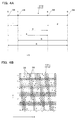
- FIG. 4A is a diagram illustrating an injection port that is one-dimensionally arranged so as to form an array of Golomb rulers that realize a minimum redundant interval
- FIG. 4B is two-dimensionally arranged so as to form a Costas array. It is a figure explaining the injection port which exists. It is a mounting example of a phased array, and is a plan view explaining a specific one-dimensional array of injection ports. It is a mounting example of a phased array, and is a plan view explaining a specific two-dimensional array of injection ports.
- FIG. 4A is a diagram illustrating an injection port that is one-dimensionally arranged so as to form an array of Golomb rulers that realize a minimum redundant interval
- FIG. 4B is two-dimensionally arranged so as to form a Costas array. It is a figure explaining the injection port which exists. It is a mounting example of a phased array, and is a plan view explaining a specific one-dimensional array of injection ports. It is a mounting example of a phased
- FIG. 7C shows an autocorrelation function in the case of an array
- FIG. 7C shows an autocorrelation function in the case of a random array.
- FIG. 8B is a diagram for explaining achievement of the number of resolution points according to the concrete example.
- FIG. 9C shows a comparison in which the emission ports are two-dimensionally arranged at equal intervals.
- FIG. It is a figure explaining formation of the light beam of (case).
- It is a conceptual block diagram explaining the phased array etc. incorporated in the light irradiation apparatus of 2nd Embodiment.
- It is a conceptual block diagram explaining the phased array etc. incorporated in the light irradiation apparatus of 3rd Embodiment.
- FIG. 15B is a one-dimensional image reconstruction by ghost imaging. It is a figure explaining a structure.
- FIG. 9 is a diagram illustrating formation of a random pattern in the case of. It is a conceptual block diagram explaining the light irradiation apparatus of 6th Embodiment.
- the light irradiation device 100 of the first embodiment shown in FIG. 1A receives a laser light B1 from the light source unit 20 that generates a laser light B1, and forms and emits irradiation light B2 having a desired wavefront state by receiving the laser light B1 from the light source unit 20.
- the light beam forming unit 30 and the control device 70 that comprehensively controls the operations of the light source unit 20 and the light beam forming unit 30 are provided.
- the light irradiation device 100 shown in FIG. 1A can be used as, for example, a projector that projects a desired light pattern, and can also be used as a laser processing device that processes an object using the irradiation light pattern.
- the light source unit 20 is composed of a coherent light source 21 such as a semiconductor laser, and is accompanied by a light source drive unit 22 which is a light source drive circuit. From the light source unit 20, laser light B1 set in various wavelength regions such as an infrared region and a visible region is emitted as a pulse wave or a continuous wave, for example.
- the coherent light source 21 is a pulsed laser
- the pulsed laser light B1 can be emitted from the light source unit 20 at precise timing.
- the light beam forming unit 30 has an optical phased array (OPA) 31 and an OPA driving unit 32.
- OPA optical phased array
- the optical phased array 31 is an optical waveguide type integrated circuit, includes a light branching section 31a and a phase adjusting section 31b on a substrate 31s, and receives the laser beam B1 from the light source section 20.
- An input unit 31c and a light output unit 31d that outputs the irradiation light B2 are provided.
- the output of the optical phased array 31 can be switched in a short time of, for example, several tens of ⁇ s or less, and illumination and processing that operate at high speed can be performed.
- the optical branching unit 31a branches the laser light B1 into M channels and guides the laser beams B1 to M waveguides 36 that are M light guiding units.
- M 8 as an example, but the value M can be set to an arbitrary natural number of 3 or more.
- the waveguides (light guide portions) 36 extend in one Z direction parallel to the XZ plane in which the substrate 31s extends and are arranged in the X direction orthogonal to the Z direction.
- a star coupler having a slab waveguide, a combination of multi-stage directional couplers, or the like can be used.
- the phase adjustment unit 31b includes M electrodes 37a that apply, for example, an electric field to the waveguides (light guide units) 36 of M channels, and a wiring 37b that enables voltage supply to each electrode 37a. ..
- the electrode 37a is formed over a predetermined width along the M waveguides 36. That is, M electrodes 37a are arranged in the X direction.
- the voltage supplied to the wiring 37b is adjusted by the OPA driving unit 32 shown in FIG. 1A so that it can be switched at high speed. By adjusting the voltage applied to each wiring 37b, the phase state of the laser beam B1 passing through each waveguide 36 can be individually controlled.
- the element lights whose phase states have been adjusted are simultaneously emitted in parallel from the respective emission ports 38 of the optical phased array 31 that have passed through the phase adjustment unit 31b, and the light output unit 31d illuminates the individual element lights combined.
- the light B2 is emitted. That is, the illumination light B2 is a light beam having a desired phase distribution or wavefront distribution in the ⁇ X directions.
- the illumination light B2 becomes a light beam that travels in a direction that forms a desired angle with respect to the Z axis, and the illumination beam B2 is a light beam with respect to the Z axis. Scanning in the XZ plane is also possible by increasing or decreasing the angle.
- the phase adjuster 31b is not limited to the electro-optic effect type modulation that adjusts the phase by the electric field strength applied to the waveguide 36, but also the carrier effect type modulation and the waveguide that adjusts the phase by injecting current into the waveguide section.
- Thermo-optical effect type modulation or the like in which the phase is adjusted by heating can be used.
- the phase adjusting unit 31b can be made small and inexpensive, the reliability can be improved, and the phase switching can be speeded up.
- the lens 100c is arranged so as to face the light output unit 31d of the optical phased array 31.
- the lens 100c has a predetermined focal length. For example, if the light output unit 31d is arranged at the front focal position of the lens 100c, the rear focal position of the lens 100c becomes a Fourier transform surface, and the rear focal point is With the position as the irradiation surface, a far-field illumination pattern corresponding to the far wavefront pattern of the illumination light B2 emitted from the light output unit 31d can be formed on the irradiation surface.
- the control device 70 has an information processing unit 71, an interface unit 72, and a storage unit 73.
- the information processing unit 71 operates the optical phased array 31 and the like via the interface unit 72, the OPA driving unit 32, and the light source driving unit 22 based on data including drive information, control information, and the like stored in the storage unit 73. Then, the illumination light B2 having a predetermined phase distribution is emitted as a predetermined pattern.
- the input/output unit 91 presents various kinds of information regarding the operating conditions and operating states of the light irradiation device 100 to the operator. The operator inputs an instruction to the control device 70 via the input/output unit 91.
- the controller 70 cooperates with the OPA driver 32 to output a control signal to the phase adjuster 31b of the optical phased array 31 to control the combined state of the lights emitted from the plurality of emission ports 38. At the same time, the composite pattern can be changed at high speed.
- the surface of the target can be laser-processed by irradiating the target with laser light in a desired irradiation pattern. Further, by operating the light irradiation device 100 under the control of the control device 70, it is possible to illuminate the surface or the like of the target with a desired irradiation pattern.
- the light output unit 31d shown in FIG. 2A is a partial extraction of the light output unit 31d shown in FIG. 1B.
- the horizontal axis represents the distance ⁇ x corresponding to the amount of parallel displacement
- the vertical axis represents the value of autocorrelation.
- FIG. 2C is a diagram illustrating an optical output unit 31d of the optical phased array 231 of the comparative example.
- Waveguides are aligned and arranged.
- the places where the waveguides are aligned and arranged gradually decrease.
- the autocorrelation has a narrow band non-flat characteristic with respect to the positional deviation, and the autocorrelation is narrowly biased. It can be said that it has become.
- FIG. 3 is a diagram for explaining the arrangement of the minimum redundant intervals realized in the light output section 31d of the optical phased array 31 shown in FIG. 1B from another aspect.
- the intensity distribution P1 of the near-field output I NFP (x) corresponding to the pattern of the illumination light B2 emitted from the plurality of emission ports 38 provided in the light output unit 31d reflects the arrangement of the emission ports 38 and has the minimum redundancy interval. It corresponds to the array of.
- the intensity distribution P2 of the hyperopic output IFFP (x') on the irradiation surface at the rear focal position by the lens 100c reflects the emission angle of the illumination light B2 from the emission port 38.
- the distribution shape P3 of the spatial spectrum S FFP (k) obtained by Fourier transforming the intensity distribution P2 of the hyperopic output I FFP (x′) corresponds to the autocorrelation in FIG. 2C. That is, by arranging the injection ports 38 at the minimum redundant interval, the distribution shape P3 of the spatial spectrum can be spread to the maximum wide band with uniform density. As a result, the light beam pattern can be formed so as to maximize the number of resolution points that can be achieved under the condition that the number of the emission ports 38 is limited. For example, under a situation where the number of injection ports 38 and the irradiation possible range (FSR: free spectral range) are fixed, finer patterns can be imaged and the spatial resolution can be efficiently improved.
- FSR free spectral range
- Arranging the plurality of emission ports 38 constituting the light output unit 31d one-dimensionally at the minimum redundant interval is to extract all combinations of the pair of emission ports 38, 38 that can be selected from the plurality of emission ports 38.
- the obtained set of intervals between the pair of injection ports 38, 38 (corresponding to a combination that realizes the discrete distance ⁇ x forming the horizontal axis in FIG. 2B) is set to have a substantially uniform degree of overlap.
- a spatially uniform spatial frequency distribution can be achieved one-dimensionally with respect to the light beam formed by the illumination light B2 emitted from the plurality of emission ports 38, so that the resolution is improved while suppressing the increase in the number of emission ports 38. Can be increased.
- the light output unit 31d forming the optical phased array 31 is one-dimensional in the X direction, and the illumination light B2 having a desired one-dimensional array phase distribution or pattern is emitted from the light output unit 31d.
- an optical phased array having the same structure as the optical phased array 31 shown in FIG. 1B can be stacked in the Y direction. With such a laminated type optical phased array, it is possible to form and emit the illumination light B2 having a two-dimensional phase distribution in the XY directions.
- the light output unit 31d includes a plurality of emission ports 38 that are two-dimensionally arranged in the XY direction (or the XZ direction when taken out in the direction perpendicular to the main surface of the substrate 38), the light output unit 31d is also included. Of the plurality of injection ports 38 are arranged two-dimensionally with a minimum redundancy interval.
- the light output section 31d or the port array 131d is arranged within the full width of the array and the distance ⁇ x in the ⁇ X direction or ⁇ Y direction which is the arrangement direction.
- the positional autocorrelations of the port array 131d before and after the translation are arranged so as to have a uniform density and a wide band as much as possible.
- Strictly two-dimensionally arranging the plurality of emission ports 38 configuring the light output unit 31d at the minimum redundant interval extracts all combinations of the pair of emission ports 38, 38 selectable from the plurality of emission ports 38.
- a spatially uniform spatial frequency distribution can be achieved two-dimensionally with respect to the light beam formed by the illumination light B2 emitted from the plurality of emission ports 38, so that the resolution can be effectively reduced while suppressing the increase in the number of emission ports 38. Can be increased.
- FIG. 4A is a diagram illustrating a specific method of arranging a plurality of emission ports 38 forming the light output unit 31d one-dimensionally with a minimum redundancy interval.
- the set of intervals of the pair of ejection ports 38, 38 obtained by extracting all the combinations of the pair of ejection ports 38, 38 that can be selected from the plurality of ejection ports 38 arranged one-dimensionally is the shortest interval.
- the reference number is 1, 2, 3, 4, 5, and 6, and includes a sequence of gradually increasing elements, and an array with a minimum redundancy interval is realized.
- the sequence shown in FIG. 4A corresponds to the sequence of the Golomb ruler.
- the plurality of emission ports 38 forming the light output section 31d are arranged one-dimensionally so as to form a Golomb ruler with the minimum redundancy of intervals.
- the array at the minimum redundant interval is not limited to the array of the strict Golomb ruler, and may be an array in which the interval between the pair of injection ports 38 is slightly overlapped or missing.
- the set of intervals of the injection ports 38 is not basically based on a single sequence of numbers, but may be a sequence of two or more sequences in which the same value is evenly repeated. Things are also included in the array with the minimum redundancy interval.
- the injection port 38 is not limited to a position that is an exact multiple of an integer with respect to the shortest interval, and a structure in which the injection port 38 is slightly shifted with respect to an integer multiple is an array with the minimum redundancy interval. include.
- FIG. 4B is a diagram for explaining a specific example in which the plurality of emission ports 38 forming the light output unit 31d are two-dimensionally arranged at the minimum redundancy interval.
- the array of the ejection ports 38 providing such a set of interval vectors realizes the array with the minimum redundant interval.
- the sequence shown in FIG. 4B corresponds to the Costas sequence. That is, the plurality of emission ports 38 forming the light output unit 31d are two-dimensionally arranged so as to form a Costas array in which the redundancy of the interval vector is minimized.
- the array at the minimum redundant interval is not limited to the array of the strict Costas ruler, but may be an array in which the interval vectors of the pair of injection ports 38 have some overlap, and the same interval vector is repeated twice. It may be composed of the above several sequences.
- FIG. 5 is a plan view illustrating a specific implementation example of the optical phased array 31 including a plurality of emission ports 38 which are one-dimensionally arranged at the minimum redundant interval.
- illustration of the optical branching unit 31a and the phase adjusting unit 31b is omitted.
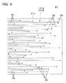
- FIG. 6 is a plan view illustrating a specific mounting example of the optical phased array 31 including a plurality of emission ports 38 that are two-dimensionally arranged at the minimum redundancy interval.
- the density ⁇ x corresponding to the positional deviation amount is substantially uniform except the position where it is zero, or the density that is as uniform as possible (that is, a substantially uniform density that is recognized as conforming to the uniform density. It can be seen that the autocorrelation distribution over a wide range is achieved by ).
- the distance ⁇ x is randomly arranged in the range of 0.5 to 1.5.
- a non-uniform and narrow autocorrelation distribution is formed around the position where the distance ⁇ x corresponding to the positional deviation amount is zero.
- FIG. 8A shows a result of performing a simulation for forming a light beam as the illumination light B2 emitted from the light irradiation device 100 shown in FIG. 1A.
- the phase adjusting unit 31b is linearly driven to form the light beam.
- the horizontal axis indicates the pixel position, and the vertical axis indicates the intensity.
- 2 shows a combined beam when one-dimensionally arranged at equal intervals equal to the minimum interval of.
- the beam width can be made extremely narrow and the resolution can be improved by arranging the injection ports 38 at the minimum redundant interval as shown by the solid line.
- the noise level becomes high when they are arranged at the minimum redundancy interval shown by the solid line.
- FIG. 8B is a diagram for explaining the relationship between the number of ejection ports and the number of resolution points.
- the solid line indicates the number of resolution points that can be formed when the ejection ports are one-dimensionally arranged at the minimum redundancy interval corresponding to the Golomb ruler, and the broken line can be formed when the ejection ports are one-dimensionally arranged at equal intervals. Indicates the number of resolution points.
- the number of resolution points indicated by the solid line increases in proportion to M 2
- the number of resolution points indicated by the broken line increases in proportion to M.
- the spot-shaped light beam having a small diameter is formed repeatedly at the FSR interval, and the beam scanning with high resolution is possible.
- the spot-shaped light beam having a small diameter is formed repeatedly at the FSR interval, and the beam scanning with high resolution is possible.
- the plurality of emission ports 38 provided in the plurality of waveguides (light guide portions) 36 are arranged at the minimum redundant interval, so that the number of emission ports 38 is reduced. While suppressing the increase, it is possible to improve the resolution of the light beam pattern that combines the lights emitted from the plurality of emission ports 38, and it is possible to increase the number of resolution points of the light beam pattern.
- the light irradiation apparatus according to the second embodiment is a modification of the first embodiment, and parts that are not particularly described are the same as those in the first embodiment.
- the light beam forming unit 30 or the optical phased array 231 incorporated in the light irradiation apparatus of the second embodiment includes a main body portion 230a having a structure similar to that of the optical phased array 31 shown in FIG. 1B, and a main body.
- the optical coupling section 230b is disposed near the optical output section 31d of the portion 230a, and the multi-core bundle fiber 230c is disposed near the optical output section of the optical coupling section 230b.
- the optical coupling part 230b is a three-dimensional optical circuit, and for example, a photonic lantern can be used.
- the optical coupling section 230b receives the illumination light B21, which is a one-dimensional optical signal emitted from the optical output section 31d of the main body section 230a, at the light incident section, and receives the one-dimensional optical signal as a two-dimensional optical signal.
- the light is converted to B22 and emitted from the light output unit.
- the multi-core bundle fiber 230c receives the illumination light B22, which is a two-dimensional optical signal emitted from the emission part of the optical coupling part 230b, at the incident end 3a and extends from a plurality of incident ports formed at the incident end 3a.
- the illumination light B2 which is a two-dimensional optical signal, is emitted from the emission end 3c.
- the plurality of injection ports 238 formed in the ejection end 3c are two-dimensionally arranged with a minimum redundant interval, for example, with a second type minimum redundant interval in which a Golomb ruler is repeated vertically and horizontally. There is. In the case of the present embodiment, it is not necessary to arrange the emission ports 38 at the minimum redundant interval in the light output section 31d of the main body portion 230a, and they are arranged at equal intervals.
- the light irradiation device according to the third embodiment is a modification of the first embodiment, and parts that are not particularly described are the same as those in the first embodiment.
- the illumination light B2 having a two-dimensional phase distribution is formed using a one-dimensional optical phased array (OPA).
- OPA optical phased array
- the light beam forming unit 30 or the optical phased array 331 incorporated in the light irradiation device of the third embodiment has a main body portion 330a having a structure similar to that of the optical phased array 31 shown in FIG. 1B, and a main body.
- the prism 330b which is a branching portion disposed on the light output portion 31d side of the portion 330a and extending along the arrangement direction of the light output portion 31d, is provided.
- the illumination light B2 emitted from the light output unit 31d via the waveguide 36 has a phase distribution in the arrangement direction of the light output unit 31d.
- the illumination light B2 is deflected through the prism 330b in the direction orthogonal to the arrangement direction of the light output units 31d, but at this time, the deflection angle differs depending on the wavelength component of the illumination light B2. Therefore, by sweeping the wavelength of the light source light B12, while scanning the beam in the direction orthogonal to the arrangement direction of the light emitting unit 31d, a desired beam is generated by the optical phased array 331 in the arrangement direction of the light emitting unit 31d. Can be formed. Alternatively, it is possible to form the illumination light B2 having a two-dimensional phase distribution divided into wavelength components by using a broadband light source.
- a diffraction grating may be used instead of the prism 330b. Further, the same effect can be obtained by integrating a diffraction grating type coupler at the light output portion 31d and extracting light in a direction perpendicular to the substrate 31s. Further, instead of using a broadband light source as the light source unit 20, a wavelength variable light source may be used to sweep the wavelength over time.
- the imaging device according to the fourth embodiment incorporates the light irradiation device of the first embodiment, and parts that are not particularly described are the same as those of the first embodiment.
- the imaging apparatus 200 of the fourth embodiment is illuminated by the illumination optical system 40 for illumination and measurement and the illumination light B2 in addition to the light irradiation apparatus 100 having the structure shown in FIG. And a light receiving element 60 that detects the intensity of the measurement light B3 from the target OB.
- the observation optical system 40 includes a branch mirror 43 and a plurality of lenses L1 and L2.
- the branch mirror 43 is a half mirror having a uniform transmittance or reflectance.
- the branch mirror 43 partially transmits the illumination light B2 from the optical phased array 31 to enter the object OB, and also reflects the measurement light B3 that is the return light reflected by the scattering on the surface OBa of the object OB. Lead to the light receiving element 60.
- the lens L1 enables illumination in the far-field state while preventing divergence of the illumination light B2 emitted from the optical phased array 31.
- the lens L2 forms an image of the measurement light B3 reflected by the target OB on the photosensitive portion 61 of the light receiving element 60.
- the light receiving element 60 is a measurement sensor that detects the intensity of the measurement light from the illuminated target.
- the light receiving element 60 has sensitivity to the wavelength of the light source unit 20 and can be provided with a wavelength selection filter.
- the light receiving element 60 is driven by the light receiving element driving unit 82 to operate, and outputs the intensity signal of the measurement light B3 incident on the photosensitive unit 61. Note that, although FIG. 13 shows an example of a system that measures the reflected light from the target OB, imaging can be similarly performed by measuring the light that has transmitted through the target OB.
- the light irradiation device 100 can operate the light beam forming unit 30 under the control of the control device 70 to two-dimensionally scan, for example, a spot-shaped light beam on the surface OBa of the target OB.
- the light-receiving element 60 is driven by the light-receiving element driving unit 82 under the control of the control device 70, and measures the change with time of the pattern signal of the measurement light B3.
- the light irradiation device 100 can measure the three-dimensional shape of the target OB from the scanning position and scanning timing of the spot-shaped light beam.
- the imaging device according to the fifth embodiment incorporates the light irradiation device according to the first embodiment, and is a partial modification of the imaging device according to the fourth embodiment. Is the same as in the first or fourth embodiment.
- an observation optical system 40 for illumination and measurement, and an irradiation state of the illumination light B2. Is included as a distribution, and a light receiving element 560 that detects the intensity of the measurement light B3 from the target OB illuminated by the illumination light B2.
- the illumination light B2 controlled in the phase state having a random phase distribution is emitted from the light output unit 31d of the optical phased array 31 of the light irradiation device 100. Further, the illumination light B2 changes at high speed in time series, and the illumination light B2, which itself has a random phase distribution, is emitted as N different patterns. That is, each of these N patterns or N types of illumination light B2 has a random phase distribution and changes randomly in time series. In each pattern, the distribution range of the random phase is ⁇ 180°, and there is no bias.
- the phase adjusting unit 31b forming the optical phased array 31 When the phase adjusting unit 31b forming the optical phased array 31 is one-dimensional in the X direction, the light output unit 31d emits the illumination light B2 having a one-dimensional random phase distribution or pattern. When the phase adjuster 31b is two-dimensional in the XY directions, the light output unit 31d can emit the illumination light B2 having a two-dimensional array of random phase distributions or patterns.
- the observation optical system 40 includes a branch mirror 43 and a plurality of lenses L1, L22, L3.
- the branch mirror 43 splits the illumination light B2 from the optical phased array 31 so that a part thereof is incident on the target OB and the rest is incident on the illumination image sensor 50.
- the branch mirror 43 also reflects the measurement light B3, which is the return light reflected by the scattering on the surface OBa of the target OB, and guides it to the light receiving element 560.
- the lens L1 enables illumination in the far-field state while preventing divergence of the illumination light B2 emitted from the optical phased array 31.
- the lens L22 reduces the luminous flux diameter of the measurement light B3 reflected by the target OB and makes it incident on the photosensitive portion 561 of the light receiving element 560 at once.
- the lens L3 cooperates with the lens L1 to form a pattern of the illumination light B2 as a far-field image on the photosensitive surface 51 of the illumination image sensor 50.
- the light receiving element 560 collectively detects the intensity of the measurement light reflected by the target OB
- the illumination image sensor 50 detects the far-field image of the illumination light emitted from the optical phased array 31.
- FIG. 14 shows an example of a system that measures the reflected light from the target OB, imaging can be performed in the same manner by measuring the light that has passed through the target OB.
- the illumination image sensor 50 is a semiconductor image sensor such as CMOS or CCD.
- the illumination image sensor 50 has sensitivity to the wavelength of the light source unit 20 and can be provided with a wavelength selection filter.
- the illumination image sensor 50 detects the pattern of the illumination light B2 formed on the photosensitive surface 51 and captures it as a detection image. At this time, the intensity value of the illumination light B2 is detected for each pixel position. As described above, since the illumination light B2 is emitted in the N pattern by the optical phased array 31, N detection images of the illumination light B2 are also obtained.
- the control device 70 operates the optical phased array 31 and the like via the interface unit 72 and the OPA drive unit 32 to emit the illumination light B2 having a random phase distribution in a plurality of patterns.
- the information processing section 71 receives the detection image captured by the illumination image sensor 50 together with the timing information via the interface section 72.
- the control device 70 receives the intensity of the measurement light B3 detected by the light receiving element 560 together with the timing information via the interface unit 72.
- the information processing unit 71 temporarily stores the detection image of the illumination light B2 acquired from the illumination image sensor 50 and the intensity value of the measurement light B3 acquired from the light receiving element 560 in the storage unit 73, and also detects these detection image and intensity.
- the state of the target OB obtained from the value is stored as a measurement result or a reconstructed image.
- the information processing section 71 causes the position information on the illumination image sensor 50 (specifically, the coordinates corresponding to the X coordinate or the XY coordinate on the object OB shown in the figure and the coordinate corresponding to the Z axis on the illumination image sensor 50).
- a value such as X is premised, and a reconstructed image is calculated from the detection information of the illumination image sensor 50 and the detection information of the light receiving element 560.
- This reconstructed image represents the state of the target OB, such as the reflectance of the target OB.
- the information processing section 71 changes the phase distribution of the illumination light B2 of the one-dimensional array from the optical phased array 31 of the one-dimensional structure N times, and the total signal intensity detected by the light receiving element 560,
- the reconstructed image O(x) is calculated from the signal intensity at the target position on the illumination image sensor 50.
- the value x corresponds to the X axis on the target OB in the apparatus configuration of FIG. 1, but corresponds to the Z axis on the illumination image sensor 50.
- the value x on the illumination image sensor 50 is a discrete value corresponding to a pixel.
- the value N indicates the number (natural number) of random patterns formed and output by the optical phased array 31.
- the value S r represents the measurement value of the light receiving element 60, that is, the intensity value of the measurement light B3.
- the value ⁇ S> indicates the average value of N values S r obtained by N times of measurements with the random pattern changed.
- I r (x) represents the relationship between the coordinate value x on the illumination image sensor 50 and the intensity value at the pixel corresponding to this coordinate value x, that is, the detected brightness.
- ⁇ means adding (S r ⁇ S>) ⁇ I r (x) while changing the variable r of the values S r and I r (x) from 1 to N.
- This reconstructed image O(x) gives the brightness value of the reconstructed image to each coordinate value x.
- Equation (1) above determines the reconstructed image O(x) with respect to the one-dimensional pixel array in the illumination image sensor 50, but the optical phased array 31 has a two-dimensional structure and the illumination image sensor 50
- a process of determining the reconstructed image O(x, y) is performed on the two-dimensional pixel array.
- the value y corresponds to the Y axis on the target OB, and also corresponds to the Y axis on the illumination image sensor 50.
- the above formula (1) or formula (2) is an example of a method (ghost imaging) for obtaining a reconstructed image of the target OB from a random illumination pattern, and statistical processing, optimization processing, etc. may be added. Alternatively, another algorithm can obtain a reconstructed image of the target OB.
- FIG. 15A and 15B are charts showing simulation results using the imaging apparatus 200 of the embodiment.
- the horizontal axis represents the pixel position, and the vertical axis represents the irradiation intensity.
- the broken line shows a one-dimensional random illumination pattern achieved by the conventional uniform arrangement, and the waveform is dull. It can be seen that the optical phased array 31 of the embodiment can form a one-dimensional random illumination pattern with extremely high precision.
- the solid line corresponds to the solid line in FIG.
- a constituent image is shown.
- the dotted line shows the original waveform to be restored, and it can be seen that extremely precise image reconstruction is possible with the optical phased array 31 of the embodiment.
- the dashed line corresponds to the dashed line in FIG. 15B and shows the reconstructed image obtained using the random illumination achieved by the conventional uniform array.
- the imaging apparatus according to the sixth embodiment is a modification of the fifth embodiment, and parts that are not particularly described are the same as in the fifth embodiment.
- the electrodes for operating the optical phased array (OPA) are simple.
- the optical phased array 631 used in the imaging apparatus of the sixth embodiment operates M waveguides 36, which are a plurality of optical paths, with electrodes 33e to 33h smaller than this.
- the seven waveguides 36 are operated by the four electrodes 33e to 33h.
- the values of the voltages V1 to V4 applied to the electrodes 33e to 33h are randomly changed.
- the illumination light B2 having a random phase distribution can be emitted from the light output unit 31d.
- the optical phased array 631 is provided with a plurality of electrodes 33e to 33h for phase adjustment which are arranged over a plurality of waveguides 36 and have random shape patterns different from each other.
- the illumination light B2 having a random phase distribution is emitted depending on the combination of the electrodes 33e to 33h.
- the present invention has been described with reference to the above embodiments, the present invention is not limited to the above embodiments.
- the illustrated array of injection ports 38 is merely exemplary, and various arrays with minimum redundant spacing are possible.
- the waveguide 36 can be replaced with a light guide such as an optical fiber, and the phase adjuster 31b can be replaced with an optical phase modulator connected to the optical fiber.
- the imaging device 200 of the embodiment that acquires a three-dimensional image can be used, for example, in the field of LIDAR (Light Detection and Ranging), and can be used to discriminate an object existing in front. Furthermore, the imaging device 200 of the embodiment can be used in fields such as barcode readers, biological imaging, and microscopes.
- LIDAR Light Detection and Ranging
Landscapes
- Physics & Mathematics (AREA)
- Optics & Photonics (AREA)
- Engineering & Computer Science (AREA)
- Nonlinear Science (AREA)
- Plasma & Fusion (AREA)
- Mechanical Engineering (AREA)
- General Physics & Mathematics (AREA)
- Chemical & Material Sciences (AREA)
- Ceramic Engineering (AREA)
- Crystallography & Structural Chemistry (AREA)
- Optical Modulation, Optical Deflection, Nonlinear Optics, Optical Demodulation, Optical Logic Elements (AREA)
- Laser Beam Processing (AREA)
Abstract
光放射点の個数に合わせて光ビームパターンの分解能を高めることができる光照射装置、並びに、これを組み込んだイメージング装置及びレーザー加工装置を提供する。 光照射装置100は、光をそれぞれ通過させる複数の導波路(導光部)36と、複数の導波路36に設けた複数の射出ポート38から射出させる光の位相を調整する位相調整部31bとを備え、複数の射出ポート38は、最小冗長間隔で配列されている。
Description
本発明は、複数の導光路から位相を制御した光を射出させる光照射装置、並びに、これを組み込んだイメージング装置及びレーザー加工装置に関する。
光照射装置として、等間隔の格子点上に配列された光放射点から位相が制御された光を射出させることで所望の光ビームパターンを形成する光フェーズドアレイ(OPA:optical phased array)が存在する(例えば、非特許文献1)。
しかしながら、等間隔の格子点上に光放射点を配置する場合、光ビームパターンにおいて距離の短い光放射点間に由来する空間周波数成分が支配的となって、光放射点の個数の割に光ビームパターンの分解能を高めることができない。
ラジオ波を受信するためのアンテナについては、リニアアレイの配列として、冗長性を減らしつつ空間周波数による感度を一様にするための配列が考察されている(非特許文献2)。
"Large-scale nanophotonic phased array" J. Sun, et al., Nature, 493, 195 (2013).
"Minimum-Redundancy Linear Arrays" Alan T. Moffet, IEEE Transactions on Antennas and Propagation Vol. AP-16, No. 2, (Mar. 1968).
本発明は、光放射点の個数に合わせて光ビームパターンの分解能を高めることができる光照射装置、並びに、これを組み込んだイメージング装置及びレーザー加工装置を提供することを目的とする。
上記目的を達成するため、本発明に係る光照射装置は、光をそれぞれ通過させる複数の導光部と、複数の導光部に設けた複数の射出ポートから射出させる光の位相を調整する位相調整部とを備え、複数の射出ポートは、最小冗長間隔で配列されている。
上記光照射装置では、複数の導光部に設けた複数の射出ポートが最小冗長間隔で配列されているので、射出ポートの数が増大するのを抑えつつ、複数の射出ポートから射出させる光を合わせた光ビームパターンの分解能を高めることができる。
本発明の具体的な側面によれば、上記光照射装置において、複数の射出ポートから同時並列的に光を射出させる。この場合、複数の射出ポートから選択した複数の組合せに対応する光ビーム成分を並列的に形成でき、多様なパターンの光ビームを形成することができる。
本発明の別の側面によれば、複数の射出ポートから選択可能な一対の射出ポートの組合せを全て抽出することによって得られる一対の射出ポートの間隔又は間隔ベクトルの集合は、略一様な重複度に設定されている。この場合、複数の射出ポートから射出される光ビームに関して略均一な空間周波数分布を達成できるので、射出ポート数の増加を抑えつつ分解能を効果的に高めることができる。
本発明のさらに別の側面によれば、複数の射出ポートの配列は、複数の射出ポートの個数を固定した場合に空間的な自己相関を略均一な密度で最大限広域にする。この場合、射出ポート数を最小限としつつ達成可能な最も多い分解可能点数で光ビームパターンを形成することができる。
本発明のさらに別の側面によれば、複数の射出ポートは、ゴロム定規を構成するように1次元に配列されている。ゴロム定規の配列は、間隔の冗長性を最小としたものとなっている。
本発明のさらに別の側面によれば、複数の射出ポートは、コスタス配列を構成するように2次元に配列されている。コスタス配列は、間隔ベクトルの冗長性を最小としたものとなっている。
本発明のさらに別の側面によれば、複数の導光部は、複数の導波路である。この場合、集積回路型の光照射装置の作製が容易になり、光照射装置のサイズの小型化や構造の簡素化を図ることができる。
本発明のさらに別の側面によれば、光源部と、光源部からの光を分岐して複数の導光部に入射させる光分岐部とをさらに備える。この場合、単一の光源によって光照射装置を動作させることができる。
本発明のさらに別の側面によれば、位相調整部に対して制御信号を出力することによって複数の射出ポートから射出させる光の合成状態を制御する制御装置をさらに備える。この場合、制御装置の制御下で光照射装置から出力される光ビームの強度パターンを所望の状態とすることができる。
本発明のさらに別の側面によれば、光源部は、連続波レーザー、もしくは、パルスレーザーを有する。この場合、光照射装置から出力される光ビームパターンを高速で切り換えて、照明、表示、処理等を一連の処理として行うことができる。
上記目的を達成するため、本発明に係るイメージング装置は、上述した光照射装置と、光照射装置から射出された光によって照明された対象からの計測光の強度を検出する計測センサーと、計測センサーによって得た検出情報から対象の状態に関する像を抽出する処理を行う情報処理部とを備える。
上記イメージング装置では、簡素ながら高分解能の光照射装置を用いており、簡素化された処理によって高精度の計測等を行うことができる。
本発明の具体的な側面によれば、上記イメージング装置において、光照射装置から射出された光の照射強度分布を検出する照明像センサーをさらに備え、光照射装置は、ランダムな位相分布の照明光を射出する。
上記目的を達成するため、本発明に係るレーザー加工装置は、上述した光照射装置と、位相調整部に対して制御信号を出力することによって複数の射出ポートから射出させる光の合成状態を制御する制御装置とを備える。
上記レーザー加工装置では、簡素ながら高分解能の光照射装置を用いており、簡素化された処理によって高精度で加工を行うことができる。
本発明の具体的な側面によれば、上記レーザー加工装置において、光源部と、前記光源部からの光を分岐して前記複数の導光部に入射させる光分岐部とをさらに備える。
〔第1実施形態〕
以下、図面を参照して、本発明に係る第1実施形態の光照射装置等について詳細に説明する。
以下、図面を参照して、本発明に係る第1実施形態の光照射装置等について詳細に説明する。
図1Aに示す第1実施形態の光照射装置100は、レーザー光B1を発生する光源部20と、光源部20からのレーザー光B1を受けて所望の波面状態の照射光B2を形成し射出する光ビーム形成部30と、光源部20及び光ビーム形成部30の動作を統括的に制御する制御装置70とを備える。図1Aに示す光照射装置100は、例えば所期の光パターンを投影するプロジェクターとして用いることができ、照射光パターンによって対象を加工するレーザー加工装置として用いることもできる。
光源部20は、半導体レーザーその他のコヒーレント光源21で構成され、光源駆動回路である光源駆動部22を付随させたものとなっている。光源部20からは、赤外域、可視域等の各種波長域に設定されたレーザー光B1が、例えばパルス波又は連続波として射出される。コヒーレント光源21がパルスレーザーである場合、光源部20から精密なタイミングでパルス状のレーザー光B1を射出させることができる。
光ビーム形成部30は、光フェーズドアレイ(OPA)31と、OPA駆動部32とを有する。
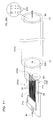
図1Bに示すように、光フェーズドアレイ31は、光導波路型の集積回路であり、基板31s上に光分岐部31aと位相調整部31bとを備え、光源部20からのレーザー光B1を受ける光入力部31cと、照射光B2を出力する光出力部31dとが設けられている。光フェーズドアレイ31は、例えば数10μs以下の短時間で出力の切り換えが可能であり、高速で動作する照明や加工が可能になる。
光フェーズドアレイ31において、光分岐部31aは、レーザー光B1をM個のチャンネルに分岐してM個の導光部であるM個の導波路36に導く。図1Bでは、一例としてM=8となっているが、値Mは、任意の3以上の自然数に設定できる。導波路(導光部)36は、基板31sが延びるXZ面に平行な一方であるZ方向に延び、Z方向に直交するX方向に配列されている。光分岐部31aとして、例えばスラブ導波路を有するスターカプラー、多段の方向性結合器を組み合わせたもの等を用いることができる。
位相調整部31bは、M個のチャンネルの導波路(導光部)36に対して例えば電界を付与するM個の電極37aと、各電極37aへの電圧供給を可能にする配線37bとからなる。電極37aは、M個の導波路36に沿った所定幅に亘って形成されている。つまり、電極37aは、X方向にM個配列されている。配線37bへの供給電圧は、図1Aに示すOPA駆動部32によって調整されて高速で切り換えが可能になっている。各配線37bに付与する電圧の調整により、各導波路36を通過するレーザー光B1の位相状態を個別に制御することができる。位相調整部31bを通過した光フェーズドアレイ31の各射出ポート38からは、位相状態が調整された要素光が同時並列的に射出され、光出力部31dからは、個々の要素光を合成した照明光B2が射出される。つまり、照明光B2は、±X方向に所望の位相分布又は波面分布を有する光ビームとされる。OPA駆動部32を介して位相調整部31bの動作を制御することにより、照明光B2は、例えばZ軸に対して所望の角度をなす方向に進行する光ビームとされ、Z軸に対する光ビームの角度を増減させることでXZ面内での走査も可能になる。
位相調整部31bについては、導波路36に与える電界強度によって位相を調整する電気光学効果型の変調に限らず、導波路部への電流注入によって位相を調整するキャリア効果型の変調、導波路を加熱することによって位相を調整する熱光学効果型の変調等を利用するものとできる。電気光学効果、キャリア効果、熱光学効果等を利用することで、位相調整部31bを小型かつ安価にでき、信頼性を高めることができ、位相の切り換えを高速化できる。
図示の例では、光フェーズドアレイ31の光出力部31dに対向してレンズ100cが配置されている。レンズ100cは、所定の焦点距離を有し、例えばレンズ100cの前側焦点位置に光出力部31dが配置されるようにすれば、レンズ100cの後側焦点位置がフーリエ変換面となり、この後側焦点位置を照射面として、この照射面上に光出力部31dから射出される照明光B2の遠方での波面パターンに対応する遠視野照明パターンを形成することができる。
制御装置70は、情報処理部71とインターフェース部72と記憶部73とを有する。情報処理部71は、記憶部73に保管された駆動情報、制御情報等を含むデータに基づいて、インターフェース部72、OPA駆動部32、及び光源駆動部22を介して光フェーズドアレイ31等を動作させ、所定の位相分布を有する照明光B2を所定のパターンとして射出させる。入出力部91には、制御装置70の制御下で、オペレーターに対して光照射装置100の動作条件や動作状態に関する種々の情報が提示される。制御装置70に対しては、入出力部91を介してオペレーターから指示が入力される。制御装置70は、OPA駆動部32と協働することにより、光フェーズドアレイ31の位相調整部31bに対して制御信号を出力することによって複数の射出ポート38から射出させる光の合成状態を制御するとともにその合成パターンを高速で変化させることができる。
制御装置70の制御下で光照射装置100を動作させることにより、対象に対して所望の照射パターンでレーザー光を照射して対象の表面をレーザー加工することができる。また、制御装置70の制御下で光照射装置100を動作させることにより、所望の照射パターンで対象の表面等を照明することができる。
図2Aに示す光出力部31dは、図1Bに示す光出力部31dを部分的に取り出したものである。光出力部31dは、例えばM=8個の射出ポート38からなるポートアレイ131dを有し、ポートアレイ131dのアレイ全幅Wは、図面上側(+X側)の一対の射出ポート38の間隔に相当する最小幅d1のM倍より大きいものとなっている。この場合、図面左側の元のポートアレイ131dと、配列方向に平行な-X方向に距離Δxだけ平行移動させた図面右側のポートアレイ131dとは、例えば距離Δx=d1の箇所で一対の導波路が一致して配列されるが、他の箇所で導波路が一致しない。距離Δxを徐々に変化させると、一対の導波路のみが一致して配列される状態がM(M-1)/2回だけ繰り返される。結果的に、図2Bに示すように、図2Aに示す最小冗長間隔のポートアレイ131dは、自己相関が位置ズレに関して均一な密度で最大限広域にし最大限広帯域に広がるものとなっている。つまり、横の位置ズレに関わらず縦の相関値が全体に亘って略一致している。より具体的にはΔx=0のピーク以外で自己相関値が等しくなっており、最も広がった状態となっている。図2Bのチャートにおいて、横軸は平行移動の位置ズレ量に対応する距離Δxを示し、縦軸は自己相関の値を示す。
図2Cは、比較例の光フェーズドアレイ231の光出力部31dを説明する図である。比較例の光出力部31dは、従来の均等配列型のものであり、例えばM=8個の射出ポート38からなり等間隔で配列されたポートアレイ231dを有する。ポートアレイ231dのアレイ全幅Wは、射出ポート38の間隔に相当する幅d2(=d1)のM倍に等しくなっている。この場合、図面左側の元のポートアレイ231dと、配列方向に平行な-X方向に距離Δxだけ平行移動させた図面右側のポートアレイ231dとは、例えば距離Δx=dの箇所でM-1個の導波路が一致して配列される。距離Δxを徐々に変化させると、導波路が一致して配列される箇所が徐々に減少する。結果的に、図2Dに示すように、図2Cに示す均等配列型のポートアレイ231dは、自己相関が位置ズレに関して狭帯域で非平坦な特性を有するものとなっており、自己相関が狭く偏ったものになっていると言える。
図3は、図1Bに示す光フェーズドアレイ31の光出力部31dにおいて実現されている最小冗長間隔の配列を別の面から説明する図である。光出力部31dに設けた複数の射出ポート38から射出される照明光B2のパターンに相当する近視野出力INFP(x)の強度分布P1は、射出ポート38の配置を反映して最小冗長間隔の配列に相当するものとなっている。レンズ100cによる後側焦点位置の照射面において、遠視出力IFFP(x')の強度分布P2は、射出ポート38からの照明光B2の射出角度を反映したものとなっている。遠視出力IFFP(x')の強度分布P2をフーリエ変換した空間スペクトルSFFP(k)の分布形状P3は、図2Cの自己相関に対応する。つまり、射出ポート38を最小冗長間隔で配置することで、空間スペクトルの分布形状P3が均一な密度で最大限広帯域に広がるようにすることができる。その結果、射出ポート38の個数に制限がある状況下で達成可能な解像点数を最大にするように光ビームパターンを形成することができる。例えば、射出ポート38の個数と照射可能範囲(FSR:free spectral range)を固定した状況下では、より細かいパターンのイメージングでき、空間分解能を効率的に向上させることができる。
光出力部31dを構成する複数の射出ポート38を1次元的に最小冗長間隔で配列することは、複数の射出ポート38から選択可能な一対の射出ポート38,38の組合せを全て抽出することによって得られる一対の射出ポート38,38の間隔の集合(図2(B)の横軸を構成する離散的な距離Δxを実現する組合せに相当)が、略一様な重複度に設定されていることに対応する。この場合、複数の射出ポート38から射出される照明光B2によって形成される光ビームに関して1次元的に略均一な空間周波数分布を達成できるので、射出ポート38の個数の増加を抑えつつ分解能を効果的に高めることができる。
以上では、光フェーズドアレイ31を構成する光出力部31dがX方向に1次元であり、光出力部31dから所望の1次元配列の位相分布又はパターンを有する照明光B2を射出させるとして説明したが、例えば図1Bに示す光フェーズドアレイ31と同様の構造の光フェーズドアレイをY方向に積層することができる。このような積層型の光フェーズドアレイによって、XY方向に2次元の位相分布を有する照明光B2を形成し射出させることができる。もしくは、導波路の構造を変更して射出ポートを基板31s上でXZ平面上に2次元配置することにより、基板31sの主面に対して垂直方向に位相を制御したレーザー光を射出させる構造とすることができる。なお、光出力部31dがXY方向に(基板38の主面に対して垂直方向に取り出す場合はXZ方向に)2次元的に配列された複数の射出ポート38を含む場合も、光出力部31dを構成する複数の射出ポート38は、最小冗長間隔で2次元配列される。2次元的に配列された複数の射出ポート38が最小冗長間隔で配列される場合、光出力部31d又はポートアレイ131dをアレイ全幅以下で配列方向である±X方向又は±Y方向に距離Δx,Δyだけ平行移動させたとき、移動前後のポートアレイ131dの位置的な自己相関が極力均一密度かつ広帯域になるように配置される。
光出力部31dを構成する複数の射出ポート38を厳密に2次元的に最小冗長間隔で配列することは、複数の射出ポート38から選択可能な一対の射出ポート38,38の組合せを全て抽出することによって得られる一対の射出ポート38,38の間隔ベクトルの集合が、略一様な重複度に設定されていることに対応する。この場合、複数の射出ポート38から射出される照明光B2によって形成される光ビームに関して2次元的に略均一な空間周波数分布を達成できるので、射出ポート38の個数の増加を抑えつつ分解能を効果的に高めることができる。
図4Aは、光出力部31dを構成する複数の射出ポート38を最小冗長間隔で1次元的に配列する具体的手法を説明する図である。この場合、1次元配列された複数の射出ポート38から選択可能な一対の射出ポート38,38の組合せを全て抽出することによって得られる一対の射出ポート38,38の間隔の集合は、最短の間隔を基準として1,2,3,4,5,及び6となっており次第に増加する要素からなる数列を含み、最小冗長間隔の配列が実現されている。射出ポート38の個数は、M=4となっているがこれに限るものではない。図4Aに示す配列は、ゴロム(Golomb)定規の配列に相当する。つまり、光出力部31dを構成する複数の射出ポート38は、間隔の冗長性を最小としたゴロム定規を構成するように1次元に配列されている。最小冗長間隔での配列は、厳密なゴロム定規の配列に限らず、一対の射出ポート38の間隔について若干の重複や欠落がある配列であってもよい。さらに、射出ポート38の間隔の集合は、単一の数列からなるものを基本とするのではなく、同じ値が均等に繰り返される2重以上の数列からなるものであってもよく、このようなものも最小冗長間隔での配列に含まれる。同様に、最短の間隔を基準として、正確に整数倍の位置に射出ポート38を配置したものに限らず、整数倍の位置に対して射出ポート38を若干ずらしたものも最小冗長間隔での配列に含まれる。
図4Bは、光出力部31dを構成する複数の射出ポート38を最小冗長間隔で2次元的に配列する具体例を説明する図である。この場合、2次元配列された複数の射出ポート38から選択可能な一対の射出ポート38,38の組合せを全て抽出することによって得られる一対の射出ポート38,38の間隔ベクトルの集合は、互いに異なるものとなっている。より具体的には、光出力部31dは、M×Mの2次元グリッド上にM個(図示の例ではM=63)の点を配置したものであり、いずれの行にも1点が配置されるとともに、いずれの列にも1点が配置され、点から点への間隔ベクトルの集合(合計M×(M-1)/2個)を考えて、すべての間隔ベクトルが互いに異なるものとなっている。このような間隔ベクトルの集合を与える射出ポート38の配列によって、最小冗長間隔の配列が実現されている。図4Bに示す配列は、コスタス(Costas)配列に相当する。つまり、光出力部31dを構成する複数の射出ポート38は、間隔ベクトルの冗長性を最小としたコスタス配列を構成するように2次元に配列されている。最小冗長間隔での配列は、厳密なコスタス定規の配列に限らず、一対の射出ポート38の間隔ベクトルについて若干の重複等がある配列であってもよく、同じ間隔ベクトルが均等に繰り返される2重以上の数列からなるものであってもよい。
図5は、最小冗長間隔で1次元配列された複数の射出ポート38を備える光フェーズドアレイ31の具体的な実装例を説明する平面図である。この場合、基板31s上にM=64個の導波路36が形成され、小冗長間隔で配列されたM個の射出ポート38からなる光出力部31dが形成されている。なお、光分岐部31aや位相調整部31bについては図示を省略してきる。図6は、最小冗長間隔で2次元配列された複数の射出ポート38を備える光フェーズドアレイ31の具体的な実装例を説明する平面図である。
図7Aは、M=12個の射出ポート38を最小冗長間隔で1次元的に配列した場合の自己相関関数を示すチャートである。この場合、位置ズレ量に対応する距離Δxがゼロの位置を除いて略均一な密度又は可能な限り均一な密度(つまり均一な密度に準じたものと認められる、実現可能な略一様な密度)で広範囲に亘る自己相関分布が達成されていることが分かる。図7Bは、M=12個の射出ポート38を等間隔で1次元的に配列した場合の自己相関関数を示すチャートである。この場合、位置ズレ量に対応する距離Δxがゼロの位置の周辺に集中した不均一で狭い自己相関分布が形成されていることが分かる。図7Cは、M=12個の射出ポート38をランダムに1次元的に配列した場合の自己相関関数を示すチャートである。ここで、距離Δxは、0.5~1.5の範囲でランダムな配置としている。この場合も、位置ズレ量に対応する距離Δxがゼロの位置の周辺に集中した不均一で狭い自己相関分布が形成されていることが分かる。
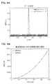
図8Aは、図1Aに示す光照射装置100から射出される照明光B2として光ビームを形成するシミュレーションを行った結果を示している。光ビームを形成するため、位相調整部31bを線形に駆動している。横軸は、画素位置を示し、縦軸は強度を示す。実線は、M=27個の射出ポート38をゴロム定規に相当する最小冗長間隔で1次元的に配列した場合の合成ビームを示し、破線は、M=27個の射出ポート38を実線のゴロム定規の最小間隔と等しい等間隔で1次元的に配列した場合の合成ビームを示す。実線で示すように射出ポート38を最小冗長間隔で配置する方が、ビーム幅を極めて細くすることができ、分解能を高め得ることが分かる。ただし、実線で示す最小冗長間隔で配置した場合、雑音レベルが高くなると認められる。
図8Bは、射出ポート数と解像点数との関係を説明する図である。実線は、射出ポートをゴロム定規に相当する最小冗長間隔で1次元的に配列した場合に形成できる解像点数を示し、破線は、射出ポートを等間隔で1次元的に配列した場合に形成できる解像点数を示す。実線で示す解像点数は、M2に比例して増加し、破線で示す解像点数は、Mに比例して増加する。つまり、射出ポートを最小冗長間隔で配列する方が射出ポートを等間隔で配列するよりも圧倒的に有利であると言える。例えばM=27個の導波路又は射出ポートを用いて最小冗長間隔で配置する場合、M=4096個の導波路又は射出ポートを用いて等間隔で配置する場合と同様の解像点数を達成できていることが分かる。
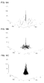
図9Aは、M=16個の射出ポート38を第1タイプの最小冗長間隔で2次元的に配列した場合の自己相関関数、具体的にはコスタス配列で2次元的に配列した場合の自己相関関数を、3D表示したチャートである。位置ズレ量に対応する距離Δx,Δyがゼロの位置を除いて略一様で広範囲に亘る自己相関分布が達成されていることが分かる。図9Bは、M=16個の射出ポート38を第2タイプの最小冗長間隔で2次元的に配列した場合の自己相関関数、具体的にはX方向にゴロム定規に従って射出ポート38を配列した1次元アレイを、Y方向にもゴロム定規の間隔で4×4(=16)のアレイ状に配列した場合の自己相関関数を、3D表示したチャートである。なお、図9Bのシミュレーションでは、図9Aと射出ポート38の最小配列間隔を一致させることで、照射パターンの範囲(FSR)が等しくなるようにしている。この場合、位置ズレ量に対応する距離Δx,Δyがゼロの位置を除いて比較的一様で広範囲に亘る自己相関分布が達成されていることが分かる。ただし、自己相関分布において規則性を持った領域が形成されていることも分かる。図9Cは、M=16個の射出ポート38を等間隔で4×4の2次元アレイ状に配列した場合の自己相関関数を、3D表示したチャートである。位置ズレ量に対応する距離Δx,Δyがゼロの位置及びその近傍に集中した不均一で狭い自己相関分布が形成されていることが分かる。
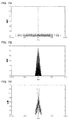
図10Aは、M=16個の射出ポート38をコスタス配列に相当する第1タイプの最小冗長間隔で2次元的に配列した場合における合成ビームの形成を示す。この場合、FSR間隔で繰り返されるスポット状で細径の光ビームが形成されており、高分解能でのビーム走査が可能であることが分かる。図10Bは、M=16個の射出ポート38をゴロム定規を縦横に繰り返した第2タイプの最小冗長間隔で4×4の2次元アレイ状に配列した場合における合成ビームの形成を示す。この場合、FSR間隔で繰り返されるスポット状で細径の光ビームが形成されており、高分解能でのビーム走査が可能であることが分かる。ただし、細径の光ビームから縦横に延びるサイドローブ状のノイズ分布が存在している。図10Cは、M=16個の射出ポート38を等間隔で4×4の2次元アレイ状に配列した場合における合成ビームの形成を示す。この場合、FSR間隔で繰り返される滲んだ状態の太い光ビームが形成されており、高分解能でビーム走査ができないことが分かる。
以上で説明した第1実施形態の光照射装置100では、複数の導波路(導光部)36に設けた複数の射出ポート38が最小冗長間隔で配列されているので、射出ポート38の数が増大するのを抑えつつ、複数の射出ポート38から射出させる光を合わせた光ビームパターンの分解能を高めることができ、かかる光ビームパターンの解像点数を高めることができる。
〔第2実施形態〕
以下、第2実施形態に係る光照射装置等について説明する。第2実施形態に係る光照射装置は、第1実施形態を変形したものであり、特に説明しない部分については、第1実施形態と同様である。
以下、第2実施形態に係る光照射装置等について説明する。第2実施形態に係る光照射装置は、第1実施形態を変形したものであり、特に説明しない部分については、第1実施形態と同様である。
図11に示すように、第2実施形態の光照射装置に組み込まれる光ビーム形成部30又は光フェーズドアレイ231は、図1Bに示す光フェーズドアレイ31と同様の構造を有する本体部分230aと、本体部分230aの光出力部31dに近接して配置される光結合部230bと、光結合部230bの光出力部に近接して配置される多芯バンドルファイバー230cとを備える。光結合部230bは、3次元光回路であり、例えばフォトニックランターンを用いることができる。光結合部230bは、本体部分230aの光出力部31dから射出された1次元の光信号である照明光B21を光入射部で受け、1次元の光信号を2次元の光信号である照明光B22に変換して光出力部から射出させる。多芯バンドルファイバー230cは、光結合部230bの射出部から射出された2次元の光信号である照明光B22を入射端3aで受け、入射端3aに形成された複数の入射ポートからそれぞれ延びる複数のファイバー(不図示)中に伝搬させ、2次元の光信号である照明光B2を射出端3cから射出させる。射出端3cに形成された複数の射出ポート238は、最小冗長間隔で2次元的に配列されており、例えばゴロム定規を縦横に繰り返した第2タイプの最小冗長間隔で2次元的に配列されている。なお、本実施形態の場合、本体部分230aの光出力部31dにおいて射出ポート38を最小冗長間隔で配置する必要はなく等間隔配列としている。
〔第3実施形態〕
以下、第3実施形態に係る光照射装置等について説明する。なお、第3実施形態に係る光照射装置は、第1実施形態を変形したものであり、特に説明しない部分については、第1実施形態と同様である。
以下、第3実施形態に係る光照射装置等について説明する。なお、第3実施形態に係る光照射装置は、第1実施形態を変形したものであり、特に説明しない部分については、第1実施形態と同様である。
第3実施形態の光照射装置では、1次元の光フェーズドアレイ(OPA)を用いて2次元の位相分布を有する照明光B2を形成する。
図12に示すように、第3実施形態の光照射装置に組み込まれる光ビーム形成部30又は光フェーズドアレイ331は、図1Bに示す光フェーズドアレイ31と同様の構造を有する本体部分330aと、本体部分330aの光出力部31d側に配置されて、光出力部31dの配列方向に沿って延びる分岐部であるプリズム330bとを備える。導波路36を経て光出力部31dから射出された照明光B2は、光出力部31dの配列方向に関して位相分布を有している。照明光B2は、プリズム330bを経て光出力部31dの配列方向に直交する方向に偏向されるが、この際、照明光B2の波長成分に応じて偏向角が異なる。従って、光源光B12の波長を掃引することで、光射出部31dの配列方向に直交する方向にビームを走査しながら、光射出部31dの配列方向には、光フェーズドアレイ331により所望のビームを形成することができる。あるいは、広帯域光源を用いることで、波長成分に分割された2次元の位相分布を有する照明光B2を形成することもできる。
プリズム330bを用いる代わりに、回折格子を用いることもできる。さらに、光出力部31dの箇所に回折格子型結合器を集積し、基板31sに対して垂直方向に光を取り出すようにしても同じ効果が得られる。また、光源部20として広帯域の光源を用いる代わりに、波長可変光源を用いて波長を経時的に掃引することもできる。
〔第4実施形態〕
以下、第4実施形態に係るイメージング装置等について説明する。なお、第4実施形態に係るイメージング装置は、第1実施形態の光照射装置を組み込んだものであり、特に説明しない部分については、第1実施形態と同様である。
以下、第4実施形態に係るイメージング装置等について説明する。なお、第4実施形態に係るイメージング装置は、第1実施形態の光照射装置を組み込んだものであり、特に説明しない部分については、第1実施形態と同様である。
図13に示すように、第4実施形態のイメージング装置200は、図1に示す構造を有する光照射装置100の他に、照明用及び計測用の観察光学系40と、照明光B2によって照明された対象OBからの計測光B3の強度を検出する受光素子60とを備える。
観察光学系40は、分岐ミラー43と、複数のレンズL1,L2とを備える。分岐ミラー43は、一様な透過率又は反射率を有するハーフミラーである。分岐ミラー43は、光フェーズドアレイ31からの照明光B2を部分的に透過させて対象OBに入射させるとともに、対象OBの表面OBaでの散乱によって反射された戻り光である計測光B3を反射して受光素子60に導く。ここで、レンズL1は、光フェーズドアレイ31から射出された照明光B2の発散を防止しつつ遠視野状態での照明を可能にする。また、レンズL2は、対象OBで反射された計測光B3を受光素子60の感光部61上に結像させる。受光素子60は、照明された対象からの計測光の強度を検出する計測センサーである。受光素子60は、光源部20の波長に感度を有しており、波長選択フィルターを付随させることができる。受光素子60は、受光素子駆動部82に駆動されて動作し、感光部61に入射した計測光B3の強度信号を出力する。なお、図13は、対象OBからの反射光を計測する系を一例として示しているが、対象OBを透過した光を計測することでも同様にイメージングを行うことができる。
光照射装置100は、制御装置70の制御下で光ビーム形成部30を動作させ、対象OBの表面OBa上で例えばスポット状の光ビームを2次元的に走査させることができる。受光素子60は、制御装置70の制御下で受光素子駆動部82に駆動されて計測光B3のパターン信号の経時的な変化を計測する。光照射装置100は、スポット状の光ビームの走査位置及び走査タイミングから、対象OBの立体的形状を計測することができる。
〔第5実施形態〕
以下、第5実施形態に係るイメージング装置等について説明する。なお、第5実施形態に係るイメージング装置は、第1実施形態の光照射装置を組み込んだものであって、第4実施形態に係るイメージング装置を部分的に変更したものであり、特に説明しない部分については、第1又は第4実施形態と同様である。
以下、第5実施形態に係るイメージング装置等について説明する。なお、第5実施形態に係るイメージング装置は、第1実施形態の光照射装置を組み込んだものであって、第4実施形態に係るイメージング装置を部分的に変更したものであり、特に説明しない部分については、第1又は第4実施形態と同様である。
図14に示すように、第5実施形態のイメージング装置200は、図1に示す構造を有する光照射装置100の他に、照明用及び計測用の観察光学系40と、照明光B2の照射状態を分布として検出する照明像センサー50と、照明光B2によって照明された対象OBからの計測光B3の強度を検出する受光素子560とを備える。
光照射装置100の光フェーズドアレイ31の光出力部31dからは、ランダムな位相分布を有する位相状態に制御された照明光B2が射出される。さらに、照明光B2は、時系列的に高速で変化し、光出力部31dからは、それ自体がランダムな位相分布を有する照明光B2が互いに異なるN個のパターンとして射出される。つまり、これらN個のパターン又はN種の照明光B2は、いずれもランダムな位相分布を有し、時系列的にもランダムに変化する。なお、各パターンにおいて、ランダムな位相の分布範囲は、±180°であり、偏りのないものとなっている。
光フェーズドアレイ31を構成する位相調整部31bがX方向に1次元の場合、光出力部31dから1次元配列のランダムな位相分布又はパターンを有する照明光B2を射出させる。位相調整部31bがXY方向に2次元の場合、光出力部31dから2次元配列のランダムな位相分布又はパターンを有する照明光B2を射出させることができる。
観察光学系40は、分岐ミラー43と、複数のレンズL1,L22,L3とを備える。分岐ミラー43は、光フェーズドアレイ31からの照明光B2を分割して、一部を対象OBに入射させるとともに、残りを照明像センサー50に入射させる。また、分岐ミラー43は、対象OBの表面OBaでの散乱によって反射された戻り光である計測光B3を反射して受光素子560に導く。ここで、レンズL1は、光フェーズドアレイ31から射出された照明光B2の発散を防止しつつ遠視野状態での照明を可能にする。また、レンズL22は、対象OBで反射された計測光B3の光束径を絞って受光素子560の感光部561に一括入射させる。レンズL3は、レンズL1と協働して照明像センサー50の感光面51に遠視野像として照明光B2のパターンを形成する。以上において、受光素子560は、対象OBで反射された計測光の強度を一括して検出し、照明像センサー50は、光フェーズドアレイ31から射出された照明光の遠視野像を検出する。なお、図14は、対象OBからの反射光を計測する系を一例として示しているが、対象OBを透過した光を計測することでも同様にイメージングを行うことができる。
照明像センサー50は、CMOS、CCD等の半導体イメージセンサーである。照明像センサー50は、光源部20の波長に感度を有しており、波長選択フィルターを付随させることができる。照明像センサー50は、感光面51に形成された照明光B2のパターンを検出し検出画像として取り込む。この際、画素位置ごとに照明光B2の強度値が検出される。上記のように、光フェーズドアレイ31によって照明光B2がNパターンで射出されるので、照明光B2の検出画像もN個得られる。
制御装置70は、インターフェース部72及びOPA駆動部32を介して光フェーズドアレイ31等を動作させ、ランダムな位相分布を有する照明光B2を複数個のパターンで射出させる。情報処理部71は、照明像センサー50によって撮影された検出画像を、タイミング情報とともにインターフェース部72を介して受け取る。制御装置70は、受光素子560によって検出された計測光B3の強度を、タイミング情報とともにインターフェース部72を介して受け取る。情報処理部71は、照明像センサー50から取得した照明光B2の検出画像や受光素子560から取得した計測光B3の強度値を一時的に記憶部73に保管するとともに、これらの検出画像や強度値から得た対象OBの状態を計測結果又は再構成画像として保管する。この際、情報処理部71は、照明像センサー50上の位置情報(具体的には、図示の対象OB上でX座標又はXY座標に対応し、照明像センサー50上でZ軸に対応する座標X等の値)を前提として、照明像センサー50の検出情報と受光素子560の検出情報から再構成画像を算出する。この再構成画像は、対象OBの反射率といった対象OBの状態を表す。
具体的には、情報処理部71は、例えば1次元構造の光フェーズドアレイ31からの1次元配列の照明光B2の位相分布をN回変化させつつ、受光素子560によって検出した総信号強度と、照明像センサー50上の対象位置における信号強度とから再構成画像O(x)を算出する。この再構成画像O(x)は、最も単純には、
O(x)
=(1/N)×Σ{(Sr-<S>)・Ir(x)} … (1)
で与えられる。ここで、値xは、図1の装置構成において対象OB上ではX軸に対応するが照明像センサー50上ではZ軸に対応する。照明像センサー50上での値xは、画素に相当するディスクリートな値となる。また、値Nは、光フェーズドアレイ31によって形成され出力されるランダムパターンの個数(自然数)を示す。値Srは、受光素子60の計測値すなわち計測光B3の強度値を示す。値<S>は、ランダムパターンを変更したN回の計測で得られたN個の値Srの平均値を示す。Ir(x)は、照明像センサー50上の座標値xと、この座標値xに対応する画素での強度値すなわち検出輝度との関係を表す。さらに、Σは、値Sr,Ir(x)の変数rを1~Nまで変化させつつ(Sr-<S>)・Ir(x)を加算することを意味する。この再構成画像O(x)は、各座標値xに対して再構成画像の輝度値を与える。
O(x)
=(1/N)×Σ{(Sr-<S>)・Ir(x)} … (1)
で与えられる。ここで、値xは、図1の装置構成において対象OB上ではX軸に対応するが照明像センサー50上ではZ軸に対応する。照明像センサー50上での値xは、画素に相当するディスクリートな値となる。また、値Nは、光フェーズドアレイ31によって形成され出力されるランダムパターンの個数(自然数)を示す。値Srは、受光素子60の計測値すなわち計測光B3の強度値を示す。値<S>は、ランダムパターンを変更したN回の計測で得られたN個の値Srの平均値を示す。Ir(x)は、照明像センサー50上の座標値xと、この座標値xに対応する画素での強度値すなわち検出輝度との関係を表す。さらに、Σは、値Sr,Ir(x)の変数rを1~Nまで変化させつつ(Sr-<S>)・Ir(x)を加算することを意味する。この再構成画像O(x)は、各座標値xに対して再構成画像の輝度値を与える。
以上の式(1)は、照明像センサー50における1次元の画素列に関して再構成画像O(x)を決定するものであるが、光フェーズドアレイ31が2次元構造を有し照明像センサー50が2次元画像を取得する場合、2次元の画素配列に関して再構成画像O(x,y)を決定する処理が行われる。この場合、再構成画像O(x,y)は、
O(x,y)
=(1/N)×Σ{(Sr-<S>)・Ir(x,y)} … (2)
で与えられる。ここで、値yは、対象OB上ではY軸に対応し、照明像センサー50上でもY軸に対応する。
O(x,y)
=(1/N)×Σ{(Sr-<S>)・Ir(x,y)} … (2)
で与えられる。ここで、値yは、対象OB上ではY軸に対応し、照明像センサー50上でもY軸に対応する。
なお、上記(1)式又は(2)式は、ランダムな照明パターンから対象OBの再構成画像を得る手法(ゴーストイメージング)の一例であり、統計的処理、適正化処理等を付加することができ、或いは別のアルゴリズムによって対象OBの再構成画像を得ることができる。
図15A及び15Bは、実施形態のイメージング装置200を用いたシミュレーション結果を示すチャートである。図15Aにおいて、実線は、M=16個の射出ポート38をゴロム定規に相当する最小冗長間隔で1次元に配列することによって得られる1次元のランダムな照明パターンを示している。横軸は、画素位置を示し、縦軸は照射強度を示す。なお、破線は、従来の均等配列によって達成される1次元のランダムな照明パターンを示しており、波形が鈍っている。実施例の光フェーズドアレイ31によって1次元のランダムな照明パターンを極めて精密に形成できることが分かる。図15Bにおいて、実線は、図15Aの実線に対応し、M=16個の射出ポート38をゴロム定規の最小冗長間隔で配列して得た1次元のランダムな照明パターンを利用して得られる再構成画像を示す。なお、点線は、復元対象である元の波形を示し、実施例の光フェーズドアレイ31によって極めて精密な画像再構成が可能であることが分かる。破線は、図15(B)の破線に対応し、従来の均等配列によって達成されるランダム照明を利用して得られる再構成画像を示す。
図16Aは、M=16個の射出ポート38をコスタス配列に相当する第1タイプの最小冗長間隔で2次元的に配列した場合におけるランダムパターンの生成を示す。この場合、細かなランダムパターンが形成されており、高分解能での画像再構成が可能であることが分かる。図16Bは、M=16個の射出ポート38をゴロム定規を縦横に繰り返した第2タイプの最小冗長間隔で4×4の2次元アレイ状に配列した場合におけるランダムパターンの形成を示す。この場合、図16Aよりも粗いが、細かなランダムパターンが形成されており、比較的高分解能での画像再構成が可能であることが分かる。図16Cは、M=16個の射出ポート38を等間隔で4×4の2次元アレイ状に配列した場合におけるランダムパターンの形成を示す。この場合、粗いパターンしか形成することができず、高分解能の画像再構成が容易でないことが分かる。
〔第6実施形態〕
以下、第6実施形態に係るイメージング装置等について説明する。なお、第6実施形態に係るイメージング装置は、第5実施形態を変形したものであり、特に説明しない部分については、第5実施形態と同様である。
以下、第6実施形態に係るイメージング装置等について説明する。なお、第6実施形態に係るイメージング装置は、第5実施形態を変形したものであり、特に説明しない部分については、第5実施形態と同様である。
第6実施形態のイメージング装置では、光フェーズドアレイ(OPA)を動作させるための電極を簡便なものとしている。
図17に示すように、第6実施形態のイメージング装置に用いる光フェーズドアレイ631は、複数の光路であるM個の導波路36をこれよりも少ない電極33e~33hで動作させる。図示の例では、7個の導波路36を4つの電極33e~33hで動作させる例となっている。この場合、各電極33e~33hに印可する電圧V1~V4の値をランダムに変化させる。これにより、光出力部31dからランダムな位相分布を有する照明光B2を射出させることができる。
第6実施形態のイメージング装置では、光フェーズドアレイ631において、複数の導波路36に亘って配置されるとともに互いに異なるランダムな形状パターンを有する位相調整用の複数の電極33e~33hを設け、これら複数の電極33e~33hの組み合わせ方によってランダムな位相分布の照明光B2を射出する。この結果、空間分解能を下げないで電極数を大幅に削減することができ、光フェーズドアレイ631の小型化が可能になり、光フェーズドアレイ631の駆動方法を簡素化することができる。
〔その他〕
以上実施形態に即して本発明を説明したが、本発明は、上記実施形態に限定されるものではない。例えば、図示した射出ポート38の配列は単なる例示であり、最小冗長間隔となる様々な配列が可能である。
以上実施形態に即して本発明を説明したが、本発明は、上記実施形態に限定されるものではない。例えば、図示した射出ポート38の配列は単なる例示であり、最小冗長間隔となる様々な配列が可能である。
導波路36については、光ファイバーのような導光路に置き換えることができ、位相調整部31bは、光ファイバーと接続した光位相変調器に置き換えるようなものとできる。
実施形態のイメージング装置200のうち、3次元画像を取得するものについては、例えばLIDAR(Light Detection and Ranging)の分野に用いることができ、前方に存在する物体を弁別するために用いることができる。さらに、実施形態のイメージング装置200は、バーコードリーダー、生体イメージング、顕微鏡等の分野に用いることもできる。
Claims (14)
- 光をそれぞれ通過させる複数の導光部と、
前記複数の導光部に設けた複数の射出ポートから射出させる光の位相を調整する位相調整部とを備え、
前記複数の射出ポートは、最小冗長間隔で配列されている、光照射装置。 - 前記複数の射出ポートから同時並列的に光を射出させる、請求項1に記載の光照射装置。
- 前記複数の射出ポートから選択可能な一対の射出ポートの組合せを全て抽出することによって得られる前記一対の射出ポートの間隔又は間隔ベクトルの集合は、略一様な重複度に設定されている、請求項1及び2のいずれか一項に記載の光照射装置。
- 前記複数の射出ポートの配列は、前記複数の射出ポートの個数を固定した場合に空間的な自己相関を略均一な密度で最大限広域にする、請求項1~3のいずれか一項に記載の光照射装置。
- 前記複数の射出ポートは、ゴロム定規を構成するように1次元に配列されている、請求項2及び3のいずれか一項に記載の光照射装置。
- 前記複数の射出ポートは、コスタス配列を構成するように2次元に配列されている、請求項2及び3のいずれか一項に記載の光照射装置。
- 前記複数の導光部は、複数の導波路である、請求項1~6のいずれか一項に記載の光照射装置。
- 光源部と、前記光源部からの光を分岐して前記複数の導光部に入射させる光分岐部とをさらに備える、請求項1~7のいずれか一項に記載の光照射装置。
- 前記位相調整部に対して制御信号を出力することによって前記複数の射出ポートから射出させる光の合成状態を制御する制御装置をさらに備える、請求項8に記載の光照射装置。
- 前記光源部は、連続波レーザー、もしくは、パルスレーザーを有する、請求項8及び9のいずれか一項に記載の光照射装置。
- 請求項1~10のいずれか一項に記載の光照射装置と、
前記光照射装置から射出された光によって照明された対象からの計測光の強度を検出する計測センサーと、
前記計測センサーによって得た検出情報から対象の状態に関する像を抽出する処理を行う情報処理部と
を備えるイメージング装置。 - 前記光照射装置から射出された光の照射強度分布を検出する照明像センサーをさらに備え、前記光照射装置は、ランダムな位相分布の照明光を射出する、請求項11に記載のイメージング装置。
- 請求項1~10のいずれか一項に記載の光照射装置と、
前記位相調整部に対して制御信号を出力することによって前記複数の射出ポートから射出させる光の合成状態を制御する制御装置と
を備えるレーザー加工装置。 - 光源部と、前記光源部からの光を分岐して前記複数の導光部に入射させる光分岐部とをさらに備える、請求項13に記載のレーザー加工装置。
Applications Claiming Priority (2)
| Application Number | Priority Date | Filing Date | Title |
|---|---|---|---|
| JP2019000901A JP7281064B2 (ja) | 2019-01-07 | 2019-01-07 | 光照射装置、イメージング装置、及びレーザー加工装置 |
| JP2019-000901 | 2019-01-07 |
Publications (1)
| Publication Number | Publication Date |
|---|---|
| WO2020145266A1 true WO2020145266A1 (ja) | 2020-07-16 |
Family
ID=71521625
Family Applications (1)
| Application Number | Title | Priority Date | Filing Date |
|---|---|---|---|
| PCT/JP2020/000162 Ceased WO2020145266A1 (ja) | 2019-01-07 | 2020-01-07 | 光照射装置、イメージング装置、及びレーザー加工装置 |
Country Status (2)
| Country | Link |
|---|---|
| JP (1) | JP7281064B2 (ja) |
| WO (1) | WO2020145266A1 (ja) |
Cited By (2)
| Publication number | Priority date | Publication date | Assignee | Title |
|---|---|---|---|---|
| US20210095957A1 (en) * | 2019-09-27 | 2021-04-01 | Asml Holding N.V. | Lithographic Apparatus, Metrology Systems, Phased Array Illumination Sources and Methods thereof |
| JP2022122284A (ja) * | 2021-02-09 | 2022-08-22 | 國立臺灣科技大學 | 調整可能な光学移相器アレイ |
Families Citing this family (3)
| Publication number | Priority date | Publication date | Assignee | Title |
|---|---|---|---|---|
| JP2023547768A (ja) * | 2020-11-11 | 2023-11-14 | アナログ フォトニクス エルエルシー | 光フェーズドアレイの光操舵 |
| WO2023027104A1 (ja) | 2021-08-25 | 2023-03-02 | 国立大学法人電気通信大学 | 波面制御装置及び補償光学装置 |
| JP7584705B1 (ja) | 2023-08-17 | 2024-11-15 | 三菱電機株式会社 | 位相調整器及び半導体光集積素子 |
Citations (3)
| Publication number | Priority date | Publication date | Assignee | Title |
|---|---|---|---|---|
| EP3106828A1 (en) * | 2015-06-16 | 2016-12-21 | Academisch Medisch Centrum | Common-path integrated low coherence interferometry system and method therefor |
| US9557585B1 (en) * | 2013-05-30 | 2017-01-31 | Hrl Laboratories, Llc | Stacked rows pseudo-randomly spaced two-dimensional phased array assembly |
| WO2018124285A1 (ja) * | 2016-12-29 | 2018-07-05 | 国立大学法人東京大学 | イメージング装置及び方法 |
-
2019
- 2019-01-07 JP JP2019000901A patent/JP7281064B2/ja active Active
-
2020
- 2020-01-07 WO PCT/JP2020/000162 patent/WO2020145266A1/ja not_active Ceased
Patent Citations (3)
| Publication number | Priority date | Publication date | Assignee | Title |
|---|---|---|---|---|
| US9557585B1 (en) * | 2013-05-30 | 2017-01-31 | Hrl Laboratories, Llc | Stacked rows pseudo-randomly spaced two-dimensional phased array assembly |
| EP3106828A1 (en) * | 2015-06-16 | 2016-12-21 | Academisch Medisch Centrum | Common-path integrated low coherence interferometry system and method therefor |
| WO2018124285A1 (ja) * | 2016-12-29 | 2018-07-05 | 国立大学法人東京大学 | イメージング装置及び方法 |
Non-Patent Citations (1)
| Title |
|---|
| DRAKAKIS ET AL.: "The Triple Autocorrelation of an m-Sequence is a Lampel Costas Array", IEEE TRANSACTIONS ON INFORMATION THEORY, vol. 58, no. 9, 13 June 2012 (2012-06-13), pages 6047 - 6053, XP011456455, DOI: 10.1109/TIT.2012.2204541 * |
Cited By (4)
| Publication number | Priority date | Publication date | Assignee | Title |
|---|---|---|---|---|
| US20210095957A1 (en) * | 2019-09-27 | 2021-04-01 | Asml Holding N.V. | Lithographic Apparatus, Metrology Systems, Phased Array Illumination Sources and Methods thereof |
| US11994808B2 (en) * | 2019-09-27 | 2024-05-28 | Asml Holding N.V. | Lithographic apparatus, metrology systems, phased array illumination sources and methods thereof |
| JP2022122284A (ja) * | 2021-02-09 | 2022-08-22 | 國立臺灣科技大學 | 調整可能な光学移相器アレイ |
| JP7292760B2 (ja) | 2021-02-09 | 2023-06-19 | 國立臺灣科技大學 | 調整可能な光学移相器アレイ |
Also Published As
| Publication number | Publication date |
|---|---|
| JP2020112582A (ja) | 2020-07-27 |
| JP7281064B2 (ja) | 2023-05-25 |
Similar Documents
| Publication | Publication Date | Title |
|---|---|---|
| JP7281064B2 (ja) | 光照射装置、イメージング装置、及びレーザー加工装置 | |
| JP6765687B2 (ja) | イメージング装置及び方法 | |
| US12429746B2 (en) | Optical beam scanning based on waveguide switching and position-to-angle conversion of a lens and applications | |
| US11448729B2 (en) | Optical deflection device and LIDAR apparatus | |
| CN114008474B (zh) | 具有多模波导光电检测器的lidar系统 | |
| CN108779905B (zh) | 多模式照明模块和相关方法 | |
| US9983395B2 (en) | Confocal microscope with a pinhole arrangement | |
| US11555926B2 (en) | Optical device, measurement device, robot, electronic apparatus, mobile object, and shaping device | |
| JP6828062B2 (ja) | ライダー装置 | |
| CN114981710B (zh) | 用于组合相干激光射束的设备、激光系统和方法 | |
| CN114114202B (zh) | 激光发射装置、包括其的激光雷达及探测方法 | |
| JP6942333B2 (ja) | 光偏向デバイス、及びライダー装置 | |
| US20160274439A1 (en) | Random access stimulated emission depletion (STED) microscopy | |
| US20150362714A1 (en) | Beam splitter apparatus, scanning observation apparatus, laser-scanning microscope, and laser-scanning endoscope | |
| KR20220116297A (ko) | 간섭성 레이저 빔을 결합하기 위한 장치, 레이저 시스템 및 방법 | |
| US20170264069A1 (en) | Laser radar system | |
| US20210191227A1 (en) | Device for deflecting laser beams | |
| US20160231575A1 (en) | Spatiotemporal focusing apparatus and method | |
| US11506839B2 (en) | Beam deflection device | |
| JP7021061B2 (ja) | 液晶可変リターダに光を分配する射出瞳拡張器 | |
| US11789250B2 (en) | Optical detection device and method for operating an optical detection device | |
| CN119845864B (zh) | 一种显微成像系统 | |
| CN117836705A (zh) | 波阵面控制装置以及补偿光学装置 | |
| RU2199729C1 (ru) | Лазерное устройство для исследования поля микрообъектов с лучевым воздействием (варианты) | |
| US20220146686A1 (en) | Laser emission apparatus and lidar-based surround sensor having a laser emission apparatus |
Legal Events
| Date | Code | Title | Description |
|---|---|---|---|
| 121 | Ep: the epo has been informed by wipo that ep was designated in this application |
Ref document number: 20738726 Country of ref document: EP Kind code of ref document: A1 |
|
| NENP | Non-entry into the national phase |
Ref country code: DE |
|
| 122 | Ep: pct application non-entry in european phase |
Ref document number: 20738726 Country of ref document: EP Kind code of ref document: A1 |