WO2020144761A1 - 積和演算器、論理演算デバイス、ニューロモーフィックデバイス及び積和演算方法 - Google Patents
積和演算器、論理演算デバイス、ニューロモーフィックデバイス及び積和演算方法 Download PDFInfo
- Publication number
- WO2020144761A1 WO2020144761A1 PCT/JP2019/000317 JP2019000317W WO2020144761A1 WO 2020144761 A1 WO2020144761 A1 WO 2020144761A1 JP 2019000317 W JP2019000317 W JP 2019000317W WO 2020144761 A1 WO2020144761 A1 WO 2020144761A1
- Authority
- WO
- WIPO (PCT)
- Prior art keywords
- product
- input
- sum
- current detection
- current
- Prior art date
- Legal status (The legal status is an assumption and is not a legal conclusion. Google has not performed a legal analysis and makes no representation as to the accuracy of the status listed.)
- Ceased
Links
Images



Classifications
-
- G—PHYSICS
- G06—COMPUTING OR CALCULATING; COUNTING
- G06F—ELECTRIC DIGITAL DATA PROCESSING
- G06F7/00—Methods or arrangements for processing data by operating upon the order or content of the data handled
- G06F7/38—Methods or arrangements for performing computations using exclusively denominational number representation, e.g. using binary, ternary, decimal representation
- G06F7/48—Methods or arrangements for performing computations using exclusively denominational number representation, e.g. using binary, ternary, decimal representation using non-contact-making devices, e.g. tube, solid state device; using unspecified devices
- G06F7/544—Methods or arrangements for performing computations using exclusively denominational number representation, e.g. using binary, ternary, decimal representation using non-contact-making devices, e.g. tube, solid state device; using unspecified devices for evaluating functions by calculation
- G06F7/5443—Sum of products
-
- G—PHYSICS
- G06—COMPUTING OR CALCULATING; COUNTING
- G06N—COMPUTING ARRANGEMENTS BASED ON SPECIFIC COMPUTATIONAL MODELS
- G06N3/00—Computing arrangements based on biological models
- G06N3/02—Neural networks
- G06N3/06—Physical realisation, i.e. hardware implementation of neural networks, neurons or parts of neurons
- G06N3/063—Physical realisation, i.e. hardware implementation of neural networks, neurons or parts of neurons using electronic means
-
- G—PHYSICS
- G06—COMPUTING OR CALCULATING; COUNTING
- G06F—ELECTRIC DIGITAL DATA PROCESSING
- G06F2207/00—Indexing scheme relating to methods or arrangements for processing data by operating upon the order or content of the data handled
- G06F2207/38—Indexing scheme relating to groups G06F7/38 - G06F7/575
- G06F2207/48—Indexing scheme relating to groups G06F7/48 - G06F7/575
- G06F2207/4802—Special implementations
Definitions
- the present invention relates to a product-sum calculator, a logical operation device, a neuromorphic device, and a product-sum calculation method.
- the weights are added to the input signal, and the sum of all of them is input to the activation function to obtain the output. Therefore, an attempt has been made to realize the product-sum calculation by an analog circuit by combining two or more memristors whose resistances change continuously and reading the total sum of the current values output from the memristors.
- the resistance value of the memristor assigned to each synapse changes so that it has a predetermined weight, and that value is retained even when the power is turned off.
- the pulse width modulation control Pulse Width Modulation: PWM
- PWM Pulse Width Modulation
- Patent Document 1 discloses a product-sum calculation device in which information written from a data line and a bit line to a variable resistance variable resistance element is stored in a capacitor as a charge amount.
- the memristor has a circuit configuration in which a parasitic capacitance and a parasitic resistance are connected in parallel as an equivalent circuit. Therefore, when an input signal, which is a voltage pulse, is input to the memristor, a transient response caused by charging the parasitic capacitance and a transient response caused by discharging from the parasitic capacitance occur. Therefore, in the above-described product-sum calculation device, in addition to the charges in the steady state in which these transient responses do not occur, the charges due to these transient responses are stored in the capacitor, so the capacitor is saturated and the product-sum Sometimes it becomes impossible to execute an operation.
- the present invention provides a product-sum calculator, a logical operation device, a neuromorphic device, and a product-sum calculation method capable of avoiding the situation where the product-sum calculation cannot be executed due to the saturation of a capacitor. To aim.
- a plurality of product calculation units that generate an output signal by multiplying an input signal corresponding to an input value by a weight and output the output signal, and a product calculation unit that receives the input signal, From the time when the first transient response resulting from the charging of the parasitic capacitance converges to a steady state, until the second transient response due to the discharge from the parasitic capacitance of the product computing unit due to the input of the input signal occurs.
- a current detection process of detecting a current output from the plurality of product calculation units with a predetermined time delay from the input signal and thereafter detecting a current output from the plurality of product calculation units at constant time intervals is executed.
- a sum calculator that calculates a value related to the sum of the output signals based on the current detected by the current detector at each constant time interval.
- each of the plurality of product operation units includes a magnetoresistive effect element that exhibits a magnetoresistive effect.
- the sum calculation unit relates a product of a total current, which is a total of currents detected by the current detection unit at each of the constant time intervals, and a coefficient time, to a total sum of the output signals. Calculate as a value.
- the coefficient time is a shortest possible length of the input signal
- the input signal has a length that is an integer multiple of the coefficient time
- the plurality of product operations are performed.
- the current detection unit executes the current detection processing at a cycle equal to the coefficient time.
- the current detection unit ends the current detection process when a time equal to a longest possible length of the input signal elapses after the current detection process is first executed.
- the current detection unit detects the current when the current detected by the current detection process is equal to the current when the input signal is not input to the plurality of product calculation units. The process is ended.
- one aspect of the present invention is a logical operation device including any one of the above-described product-sum operation units.
- one aspect of the present invention is a neuromorphic device including any one of the above-described product-sum calculators.
- a product-sum calculation method using any one of the product-sum calculators described above wherein a plurality of product calculators are used to weight an input signal corresponding to an input value.
- the product calculation step of multiplying to generate the output signal and outputting the output signal, and the first transient response resulting from the charging of the parasitic capacitance of the product calculation section due to the input of the input signal converges and becomes a steady state.
- a plurality of the product calculating units are delayed by a predetermined time from the input signal.
- the product-sum calculation unit the logical operation device, the neuromorphic device, and the product-sum calculation method described above, it is possible to avoid the situation where the product-sum calculation cannot be executed due to the saturation of the capacitor, A logical operation device, a neuromorphic device, and a product-sum operation method can be provided.
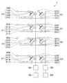
- FIG. 1 is a diagram showing an example of a part of the configuration of the product-sum calculator according to the embodiment.
- the product-sum calculator 1 includes product calculators 111, 121, 211, 221, 321, 321,..., K11, k21, input units 101E, 201E, 301E,..., K01E, and currents.
- the detection units 10D and 20D and the sum operation units 10S and 20S are provided.
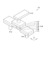
- FIG. 2 is a diagram showing an example of the resistance change element according to the embodiment.
- the product calculation unit 111 is a resistance change element, for example, the magnetoresistive effect element shown in FIG. As shown in FIGS. 1 and 2, the product calculation unit 111 includes a variable resistor 111R, a read terminal 111X, a common terminal 111Y, and a write terminal 111Z. Further, the product arithmetic units 121, 211, 221, 311, 321,..., K11, k21 shown in FIG. 1 are resistance change elements, for example, magnetoresistive effect elements similar to those shown in FIG.
- 121R, 211R, 221R, 321R, 321R,..., K11R, k21R, read terminals 121X, 211X, 221X, 311X, 321X,..., K11X, k21X and common terminals 121Y, 211Y, 221Y, 311Y, 321Y,. k11Y and k21Y and write terminals 121Z, 211Z, 221Z, 311Z, 321Z,..., K11Z, k21Z are provided.
- the product operation unit 111 will be described as an example as appropriate, but the same applies to the other product operation units 121, 211, 221, 311, 321,..., K11, k21.
- variable resistor 111R included in the product calculation unit 111 includes, for example, as illustrated in FIG. 2, a magnetization fixed layer 1111, a nonmagnetic layer 1112, a first region 1113, a domain wall 1114, and a second region 1115. , A first magnetization supply layer 1116 and a second magnetization supply layer 1117.
- the x axis, the y axis, and the z axis shown in FIG. 2 are used.
- the x-axis, y-axis, and z-axis form right-handed three-dimensional Cartesian coordinates.
- the magnetization fixed layer 1111, the nonmagnetic layer 1112, the first region 1113, the second region 1115, the first magnetization supply layer 1116, and the second magnetization supply layer 1117 are formed in a thin rectangular parallelepiped shape in the z-axis direction and have the largest area.
- the large surface is parallel to the xy plane and is electrically and magnetically connected to the first region 1113 and the second region 1115.
- the magnetization fixed layer 1111, the nonmagnetic layer 1112, the first region 1113 and the second region 1115, the first magnetization supply layer 1116, and the second magnetization supply layer 1117 are stacked in this order from the +z direction to the ⁇ z direction.
- the laminating directions may be reversed. When the stacking directions of these are reversed, the read terminal 111X is provided on the ⁇ z direction side, and the common terminal 111Y and the write terminal 111Z are provided on the +z direction side.
- the magnetization direction of the magnetization fixed layer 1111 is fixed in the +z direction or the ⁇ z direction.
- the magnetization being fixed means that the magnetization direction does not change at the time of initialization for introducing the domain wall 1114 and before and after writing using a write current.
- the magnetization fixed layer 1111 may be, for example, an in-plane magnetization film having in-plane magnetic anisotropy or a perpendicular magnetization film having perpendicular magnetic anisotropy.
- the surface facing the +z direction is in contact with the surface facing the ⁇ z direction of the magnetization fixed layer 1111, and the surfaces facing the ⁇ z direction are the first region 1113 and the second region. It is in contact with 1115.
- the surface of the magnetization fixed layer 1111 facing the ⁇ z direction side and the surface of the nonmagnetic layer 1112 facing the +z direction side have the same shape and area.
- the nonmagnetic layer 1112 may be spread so as to cover the surface of the first region 1113 facing the +z direction and the surface of the second region 1115 facing the +z direction more widely than in the case shown in FIG.
- the nonmagnetic layer 1112 is used by the product calculation unit 111 to read a change in the magnetization state of the magnetization free layer with respect to the magnetization fixed layer 1111 as a change in resistance value.
- the first region 1113, the domain wall 1114 and the second region 1115 form a magnetization free layer.
- the magnetization free layer is made of a ferromagnetic material.
- the magnetization directions of the first region 1113 and the second region 1115 are opposite to each other in the direction parallel to the z-axis.
- the domain wall 1114 is sandwiched between the first region 1113 and the second region 1115 in the direction parallel to the y axis.
- the first magnetization supply layer 1116 preferably does not overlap the magnetization fixed layer 1111 in the direction parallel to the z axis, and the surface facing the +z direction is in contact with the surface facing the ⁇ z direction of the first region 1113. ing. Further, the first magnetization supply layer 1116 has a function of fixing the magnetization direction in a range overlapping with the first magnetization supply layer 1116 in the direction parallel to the z axis in the first region 1113 to a desired direction. Further, the write terminal 111Z is connected to the surface of the first magnetization supply layer 1116 facing the ⁇ z direction.
- the first magnetization supply layer 1116 is, for example, the same material as the ferromagnetic material that can be used for the magnetization fixed layer 1111, an antiferromagnetic material such as IrMn, and a ferromagnetic material sandwiching a nonmagnetic intermediate layer such as Ru and Ir. , A material having a synthetic antiferromagnetic structure including a non-magnetic material and a ferromagnetic material.
- the second magnetization supply layer 1117 preferably does not overlap the magnetization fixed layer 1111 in the direction parallel to the z-axis, and the surface facing the +z direction is in contact with the surface facing the ⁇ z direction of the second region 1115. ing. Further, the second magnetization supply layer 1117 has a function of fixing the magnetization direction in a range overlapping with the second magnetization supply layer 1117 in the second region 1115 in the direction parallel to the z-axis to a desired direction. Further, the common terminal 111Y is connected to the surface of the second magnetization supply layer 1117 facing the ⁇ z direction.
- the first magnetization supply layer 1116 is, for example, the same material as the ferromagnetic material that can be used for the magnetization fixed layer 1111, an antiferromagnetic material such as IrMn, and a ferromagnetic material sandwiching a nonmagnetic intermediate layer such as Ru and Ir. , A material having a synthetic antiferromagnetic structure including a non-magnetic material and a ferromagnetic material.
- the magnetization fixed layer 1111, the first region 1113, the second region 1115, the first magnetization supply layer 1116, and the second magnetization supply layer 1117 are not only magnetized in the directions parallel to the z-axis but also in the x direction. It may be parallel to the axis or parallel to the y-axis. Even in this case, it is desirable that the magnetization direction of the magnetization fixed layer 1111 and the magnetization directions of the first region 1113, the second region 1115, the first magnetization supply layer 1116, and the second magnetization supply layer 1117 be parallel.
- the magnetization direction of the magnetization fixed layer 1111 is +y direction
- the magnetization direction of the first region is +y direction
- the magnetization direction of the second region is ⁇ y direction
- the magnetization direction of the first magnetization supply layer 1116 is +y direction
- the magnetization direction of the second magnetization supply layer 1117 is the ⁇ y direction.
- the product calculation unit 111 changes the position of the domain wall 1114 in the direction parallel to the y-axis by adjusting the magnitude and time of the write current flowing between the common terminal 111Y and the write terminal 111Z.
- the product calculation unit 111 can continuously change the ratio of the areas of the regions in which the magnetization directions are parallel and the regions in which the magnetization directions are anti-parallel, and can change the resistance value of the variable resistor 111R substantially linearly. .
- the region in which the magnetization directions are parallel is the area of the portion of the first region 1113 that overlaps with the magnetization fixed layer 1111 in the direction parallel to the z-axis.
- the region in which the magnetization direction is antiparallel is the area of the portion of the second region 1115 that overlaps with the magnetization fixed layer 1111 in the direction parallel to the z axis.
- the write current is input to the write terminal 111Z.
- the magnitude and time of the write current is adjusted by at least one of the number and time of current pulses.
- the product calculation units 111, 121, 211, 221, 311, 321,..., K11, k21 may be tunnel magnetoresistive elements.
- the tunnel magnetoresistive effect element includes a magnetization fixed layer, a magnetization free layer, and a tunnel barrier layer as a nonmagnetic layer.
- the magnetization fixed layer and the magnetization free layer are made of a ferromagnetic material and have magnetization.
- the tunnel barrier layer is sandwiched between the magnetization fixed layer and the magnetization free layer.
- the tunnel magnetoresistive effect element can change the resistance value by changing the relationship between the magnetization of the magnetization fixed layer and the magnetization of the magnetization free layer.
- the input unit 101E is connected to the read terminals 111X and 121X.
- the input unit 201E is connected to the read terminals 211X and 221X shown in FIG. 1
- the input unit 301E is connected to the read terminals 311X and 321X, and the read terminals k11X and k21X are connected to each other.
- the input unit k01E is connected.
- the input unit 101E inputs the input signal corresponding to the input value to the read terminals 111X and 121X.
- the input unit 201E inputs the input signal corresponding to the input value to the read terminals 211X and 221X.
- the input unit 301E inputs the input signal corresponding to the input value to the read terminals 311X and 321X.
- the input unit k01E inputs the input signal corresponding to the input value to the read terminals k11X and k21X.
- Each of these input signals is a voltage signal that has undergone pulse width modulation (PWM) according to the input value.
- PWM pulse width modulation
- the product calculation unit 111 multiplies an input signal corresponding to an input value by a weight to generate an output signal, and outputs the output signal. That is, the product calculation unit 111 reads the resistance value of the variable resistor 111R as a weight, performs a product calculation on the input signal input to the read terminal 111X to generate an output signal, and outputs the output signal from the common terminal 111Y. .. Similarly, the product operation units 121, 211, 221, 321, 321, 321,..., K11, k21 multiply the input signals corresponding to the input values by weights to generate output signals, and output the output signals.
- the current detection unit 10D From the time when the first transient response converges to a steady state until the time when the second transient response due to the discharge from the parasitic capacitance of the product calculation unit due to the input of the input signal occurs, the current detection unit 10D: A current detection process of detecting currents output by a plurality of product calculation units with a predetermined time delay from the input signal and detecting currents output by the product calculation units 111, 211, 311,... To do. Similarly, from the time when the first transient response converges to a steady state, the current detection unit 20D continues from the time when the second transient response due to the discharge from the parasitic capacitance of the product calculation unit due to the input of the input signal occurs.
- the currents output by the plurality of product computing units are detected with a predetermined time delay, and thereafter the currents are detected by the product computing units 121, 221, 321,..., K21 at a constant interval time. Execute the process. Details of the current detectors 10D and 20D will be described later.
- the sum calculator 10S calculates a value related to the sum of output signals based on the current detected by the current detector 10D at regular time intervals.
- the sum calculator 20S calculates a value related to the sum of output signals based on the current detected by the current detector 20D at regular time intervals. Details of the sum operation units 10S and 20S will be described later.
- FIG. 3 is a diagram showing an example of an equivalent circuit of a part of the configuration of the product-sum calculation unit according to the embodiment.
- the product calculation unit 111 includes a parasitic capacitance 111C and a parasitic resistance 111P as an equivalent circuit of the magnetoresistive effect element, the parasitic capacitance 111C is connected in parallel to the variable resistor 111R, and the parasitic resistance 111P is variable. It can be considered to be connected in series to the resistor 111R.
- the product calculators 121, 211, 221, 311, 321,..., K11, k21 respectively have parasitic capacitances 121C, 211C, 221C, 311C, 321C,..., K11C, k21C and parasitic resistances 121P, 211P, 221P. , 311P, 321P,..., K11P, k21P.
- wiring resistors 111W, 121W, 211W, 221W, 311W, 321W,..., K11W, k21W are connected in series to the product calculation units 111, 121, 211, 221, 321, 321, 321,..., K11, k21, respectively. Can be considered
- FIG. 4 is a diagram illustrating an example of an input signal input to the product calculation unit according to the embodiment.
- the input unit 101E outputs, for example, the input signal V1 shown in FIG.
- the input unit 201E outputs, for example, the input signal V2 shown in FIG.
- the input unit 301E outputs, for example, the input signal V3 shown in FIG.
- the input signal V1 is a voltage pulse having a pulse time of 0.1 mV and a coefficient time, for example, a length of 20 [ns]. This 20 [ns] is an example of the shortest possible length of the input signal.
- the input signal V2 is a voltage pulse having a pulse height of 0.1 mV and a length of 40 [ns] which is twice the coefficient time.
- the input signal V3 is a voltage pulse having a pulse height of 0.1 mV and a length of 80 [ns] which is four times the length of the coefficient time.
- the time when the input signal V1 is input to the product operation unit 111, the time when the input signal V2 is input to the product operation unit 211, and the time when the input signal V3 is input to the product operation unit 311 are as shown in FIG. In both cases, the time is t0. That is, the input signal V1, the input signal V2, and the input signal V3 are simultaneously input to the product calculation units 111, 211, and 321, respectively.
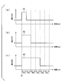
- FIG. 5 is a diagram showing an example of an output signal output from the product calculation unit according to the embodiment.
- the output signal A1 shown in FIG. 5A is input to the current detection unit 10D.
- the output signal A2 shown in FIG. 5B is input to the current detection unit 10D.
- the output signal A3 shown in FIG. 5C is input to the current detection unit 10D.
- the output signal A1 shown in FIG. 5(a) is a current signal including the first transient response T11, the steady portion S1, and the second transient response T12.
- the first transient response T11 is a transient response caused by charging the parasitic capacitance 111C of the product calculation unit 111 due to the input of the input signal V1.
- the steady-state part S1 outputs a steady-state current C[nA] from the time when the generation of the first transient response T11 of the output signal A1 ends to the time when the generation of the next second transient response T12 starts. It is the part that is.
- the second transient response T12 is a transient response caused by the discharge from the parasitic capacitance 111C of the product calculation unit 111 due to the input of the input signal V1.
- the length of the first transient response T11 and the length of the second transient response T12 are almost negligibly shorter than the length of the stationary portion S1. Further, the length of the output signal A1 is approximately the same as the time obtained by adding the transient response due to the discharge from the parasitic capacitance 111C to 20 [ns] which is the length of the input signal V1.
- the output signal A2 shown in FIG. 5(b) is a current signal including the first transient response T21, the steady portion S2, and the second transient response T22.
- the first transient response T21 is a transient response caused by charging the parasitic capacitance 211C of the product calculation unit 211 due to the input of the input signal V1.
- a steady current [nA] flows from the time when the generation of the first transient response T21 of the output signal A2 ends to the time when the generation of the next second transient response T22 starts. It is a part.
- the second transient response T22 is a transient response resulting from the discharge from the parasitic capacitance 211C of the product calculation unit 211 due to the input of the input signal V2.
- the length of the first transient response T21 and the length of the second transient response T22 are almost negligible compared to the length of the stationary portion S2. Further, the length of the output signal A2 is approximately the same as the time obtained by adding the transient response due to the discharge from the parasitic capacitance 211C to 40 [ns] which is the length of the input signal V2.
- the output signal A3 shown in FIG. 5(c) is a current signal including the first transient response T31, the steady portion S3, and the second transient response T32.
- the first transient response T31 is a transient response due to the charging of the parasitic capacitance 311C of the product calculation unit 311 due to the input of the input signal V3.
- the steady-state unit S3 outputs a steady-state current C[nA] from the time when the generation of the first transient response T31 of the output signal A3 ends to the time when the generation of the next second transient response T32 starts. It is the part that is.
- the second transient response T32 is a transient response resulting from the discharge from the parasitic capacitance 311C of the product calculation unit 311 due to the input of the input signal V3.
- the length of the first transient response T31 and the length of the second transient response T32 are almost negligible compared to the length of the stationary portion S3. Further, the length of the output signal A3 is approximately the same as the length of the input signal V3, which is 80 [ns] plus the transient response due to the discharge from the parasitic capacitance 311C.
- the first transient response T11, the first transient response T21, and the first transient response T31 have almost the same length and height. It becomes a transient response, and the second transient response T12, the second transient response T22, and the second transient response T32 are transient responses having almost the same length and height.
- FIG. 6 is a diagram showing an example of a current input to the current detection unit according to the embodiment.
- the current signal A is input to the current detection unit 10D.
- the current signal A has a first transient response T4, a steady portion S41, a second transient response T41, a steady portion S42, a second transient response T42, a steady portion S43, and a second transient response T42.
- a transient response T43 is a diagram showing an example of a current input to the current detection unit according to the embodiment.
- the first transient response T4 is a transient response generated by adding the first transient response T11, the first transient response T21, and the first transient response T31 shown in FIG.
- the steady part S41 is a part where a steady current 3C [nA] flows by adding the steady part S1, the steady part S2, and the steady part S3 shown in FIG.
- the second transient response T41 is a transient response generated by adding the steady part S2 and the steady part S3 to the second transient response T12 shown in FIG.
- the steady part S42 is a part in which a steady current 2C [nA] is flowing by adding the steady part S2 and the steady part S3 shown in FIG.
- the second transient response T42 is a transient response generated by adding the stationary portion S3 to the second transient response T22 shown in FIG.
- the steady part S43 is a part in which a steady current 1C [nA] is flowing, like the steady part S3.
- the second transient response T43 is the second transient response T32 shown in FIG.
- the current detection unit 10D is a product calculation unit for each coefficient time from the time when the generation of the first transient response or the second transient response described above ends to the time when the generation of the next first transient response or the second transient response starts.
- a current detection process for detecting the current output by 111, 211, 311 is executed.
- the coefficient time referred to here is, for example, a period corresponding to the stationary portion S41, the stationary portion S42, and the stationary portion S43 shown in FIG.
- the current detection unit 10D first detects the current 3C [nA] at a time point that is delayed from the time t0 by a fixed time, for example, 10 [ns]. Then, as indicated by points D2, D2, D3, D4, D5, and D6 in FIG. 6, the current detection unit 10D uses the current 2C[nA] at the above-described coefficient time, for example, 20 [ns] cycle. ], 1C[nA], 1[nA], 0[nA] and 0[nA] are detected.
- the current detection unit 10D ends the current detection process when the current detected by the current detection process is equal to the current when the input signal is not input to the product calculation units 111, 211, 311,..., K11. ..
- the current detection unit 10D detects the current 0 [nA] in the fifth cycle, as indicated by the point D5 in FIG. 6, the current detection process is stopped at the point D6 in the sixth cycle and the seventh and subsequent cycles. ..
- the current detection unit 10D ends the current detection process when the time equal to the longest possible length of the input signal has elapsed since the current detection process was first executed. For example, if the length of the input signal can be any one of 1, 2, 3,..., 254, 255, 256 times the shortest length of the input signal, the current detection unit 10D starts from the 257th cycle. Stops the current detection process.
- the current detection process is executed when 10 [ns] has elapsed from the start time of each cycle, but the current detection process is executed at another timing. It may be executed.
- FIG. 7 is a diagram for explaining the timing at which the current detection unit according to the embodiment executes the current detection process.
- the first transient response T4 occurs as described with reference to FIG. As shown in FIG. 7, the first transient response T4 reaches a current larger than the current 3C[nA] and then converges to the current 3C[nA].
- the state where the magnitude of the current is within the range of 3C- ⁇ [nA] to 3C+ ⁇ [nA] is the steady state where the steady current flows.
- the magnitude of ⁇ [nA] is, for example, preferably 10% pp of the current 3 [nA], and more preferably 5% pp of the current 3 [nA].
- the magnitude of the current falls within the range at time t1.
- the time from time t0 to time t1 is also called the convergence time.
- the resistance value R and the electrostatic capacitance C of the parasitic resistance are determined by inputting a plurality of rectangular voltage pulses having different pulse lengths to at least one of the product calculation units 111, 211, 311,... It can be calculated by evaluating.
- the convergence time of the first transient response described above is equal to the time required for discharging from the parasitic capacitance, and can be calculated using the following formula (1).
- the convergence time of the above-mentioned second transient response is equal to the time required for discharging from the parasitic capacitance, and can be calculated using the following formula (2).
- the second transient response T41 starts to occur at time 20 [ns]. Therefore, the stationary unit 41 described above occurs in the period from time t1 to time 20 [ns].
- the current detection unit 10D executes the current detection processing at the stationary unit 41, that is, at any timing in the period from time t1 to time 20 [ns]. Further, by determining the time so that the period from the time t1 to the time 20 [ns] is longer than the convergence time calculated by the above-mentioned time constant ⁇ , the current detection unit 10D can reliably operate in the steady unit 41. The current detection process can be executed.
- the current obtained by the current detection processing executed by the current detection unit 10D may be converted into digital data by analog-digital conversion and stored in a storage medium. Further, the current detection unit 10D may detect the current at a predetermined time in the time from the time when the first transient response converges to a steady state to the time before the second transient response occurs, or the current may be detected at a predetermined time. The current may be detected in the meantime. Further, when the current detection unit 10D detects a current during a predetermined period, the current detection process may use a statistical value of the detected current, for example, an average value or a median value.
- the sum calculator 10S calculates the product of the total current, which is the sum of the currents detected by the current detector 10D at regular time intervals, and the coefficient time as a value related to the sum of the output signals.
- the sum calculation unit 10S uses the currents 3C[nA] and 2C[nA] detected at the times indicated by points D1, D2, D2, D3, D4, D5, and D6 in FIG.
- the total current 7[nA] of C[nA], C[nA], 0[nA] and 0[nA] is calculated.
- the sum calculation unit 10S calculates the product of the total current 7 [nA] and 20 [ns], which is an example of the coefficient time, as a value related to the sum of the output signals.
- the sum operation unit 10S is an example of coefficient time of 20 [ns] for each of the currents 3C[nA], 2C[nA], C[nA], C[nA], 0[nA], and 0[nA].
- the value associated with the sum of the output signals is calculated by calculating the sum of the six products.
- the value related to the total sum of the output signals calculated by these two methods corresponds to the area of the region shown by the diagonal lines in FIG. 6, and is in a proportional relationship with the total sum of the output signals.
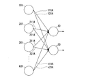
- FIG. 8 is a diagram for explaining an example of the neural network calculation executed by the product-sum calculation unit according to the embodiment.
- the nodes 101, 201, 301,..., K01 form an input layer.
- the perceptrons 10 and 20 form a hidden layer or an output layer.
- the node 101 corresponds to the input unit 101E shown in FIGS. 1 and 3, and outputs an input value corresponding to the input signal to the perceptrons 10 and 20.
- the nodes 201, 301,..., K01 correspond to the input units 201E, 301E,..., K01E, respectively, and output input values corresponding to the input signals to the perceptrons 10, 20.
- the arrow 111A corresponds to the product calculation unit 111, and indicates that the input value output from the node 101 is multiplied by the weight and the value corresponding to the output signal is input to the perceptron 10.
- an arrow 121A corresponds to the product calculation unit 121, and indicates that the input value output from the node 101 is multiplied by the weight and the value corresponding to the output signal is input to the perceptron 20.
- the perceptron 10 corresponds to the current detection unit 10D and the sum calculation unit 10S shown in FIGS. 1 and 3, and the output signals output from the arrows 111A, 211A, 311A,..., K11A are added to the added signal. Then, the current detection process described above is executed to calculate a value related to the total sum of the output signals. Then, the perceptron 10 performs activation function processing on the value and outputs the value.
- the product-sum calculator 1 has been described above. Since the product-sum calculator 1 calculates the value related to the sum of the output signals based on the current detected at regular time intervals, it is not necessary to include a capacitor for accumulating charges. Therefore, the product-sum calculation unit 1 can avoid that the capacitor is saturated and the product-sum calculation cannot be executed. Further, the sum-of-products calculator 1 can omit the capacitor, so that it is possible to realize space saving and cost saving by reducing the circuit scale.
- At least one of the product operation units 111, 121, 211, 221, 311, 321,..., K11, k21 included in the product-sum operation unit 1 includes a magnetoresistive effect element exhibiting a magnetoresistive effect. Since the magnetoresistive effect element has a larger parasitic capacitance than other variable resistance elements, it is more likely to cause saturation of the capacitor due to a transient response than other variable resistance elements. Therefore, when the magnetoresistive effect element is included as the product calculation unit described above, the above-described effects are particularly useful.
- the shortest possible length of the input signal is the coefficient time, which is an integral multiple of the coefficient time, and the product calculation units 111, 121, 211, 221, 311 and 321. ,..., k11 and k21 are simultaneously input. Then, the sum-of-products arithmetic unit 1 executes the current detection process in a cycle equal to the coefficient time. Therefore, the product-sum calculator 1 can surely detect the current when the first transient response and the second transient response have converged to be in a steady state, and execute the accurate product-sum calculation. ..
- the product-sum calculator 1 ends the current detection process when the time equal to the longest possible length of the input signal has elapsed since the current detection process was first executed. Therefore, the product-sum calculation unit 1 can keep the time for executing the current detection process constant and simplify the process.
- the product-sum calculation unit 1 operates when the current detected by the current detection process is not input to the plurality of product calculation units 111, 121, 211, 221, 311, 321,..., K11, k21. When it is equal to the current, the current detection process is ended. Therefore, the product-sum calculator 1 can end the current detection process early.
- the time when the input signal V1 is input to the product calculation unit 111, the time when the input signal V2 is input to the product calculation unit 211, and the time when the input signal V3 is input to the product calculation unit 311 are set.
- the time is t0, but the present invention is not limited to this. That is, the times at which these three input signals are input may be different from each other.
- the coefficient time may be a period from the time when the generation of the first transient response or the second transient response ends to the time when the generation of the next first transient response starts.
- the product-sum calculator 1 described above may be included in a logical operation device or a neuromorphic device.
- the logical operation device mentioned here is a logical circuit formed by combining a plurality of product-sum operation units 1, for example, an AND circuit and an OR circuit.
- the logical operation here is a concept including deep learning.
- the neuromorphic device referred to here is a device to which a structure of the brain and a mechanism of firing neurons called neurons are applied, and is used for machine learning and the like.
- a program for realizing the function of each device such as the product-sum calculator 1 according to the above-described embodiment is recorded in a computer-readable recording medium, and the program recorded in this recording medium is read by a computer system.
- the processing may be performed by executing the above.
- the computer system mentioned here may include an operating system (OS) or hardware such as peripheral devices.
- the computer-readable recording medium is, for example, a writable non-volatile memory such as a floppy disk, a magneto-optical disk, a ROM (Read Only Memory), a flash memory, a portable medium such as a DVD (Digital Versatile Disc),
- a storage device such as a hard disk built in the computer system, or a volatile memory inside the computer system that serves as a server or a client when the program is transmitted via a network or a communication line, and holds the program for a certain period of time. Also includes.
- the above-described program may be transmitted from a computer system that stores the program in a storage device or the like to another computer system via a transmission medium or by a transmission wave in the transmission medium.
- the transmission medium for transmitting the program refers to a medium having a function of transmitting information, such as a network such as the Internet or a communication line such as a telephone line.
- the above-mentioned program may be a program for realizing a part of the above-described functions, and a program that can realize the above-mentioned functions in combination with a program already recorded in the computer system, that is, a so-called difference program. It may be.
- the above-mentioned program is read and executed by a processor such as a CPU (Central Processing Unit) included in the computer.
- a processor such as a CPU (Central Processing Unit) included in the computer.
Landscapes
- Engineering & Computer Science (AREA)
- Physics & Mathematics (AREA)
- Theoretical Computer Science (AREA)
- General Physics & Mathematics (AREA)
- General Engineering & Computer Science (AREA)
- Computing Systems (AREA)
- Life Sciences & Earth Sciences (AREA)
- Health & Medical Sciences (AREA)
- Biomedical Technology (AREA)
- Biophysics (AREA)
- Pure & Applied Mathematics (AREA)
- Mathematical Analysis (AREA)
- Computational Mathematics (AREA)
- Mathematical Optimization (AREA)
- Neurology (AREA)
- Molecular Biology (AREA)
- Mathematical Physics (AREA)
- Software Systems (AREA)
- General Health & Medical Sciences (AREA)
- Evolutionary Computation (AREA)
- Data Mining & Analysis (AREA)
- Computational Linguistics (AREA)
- Artificial Intelligence (AREA)
- Amplifiers (AREA)
- Measurement Of Current Or Voltage (AREA)
Abstract
Description
図1及び図2を参照しながら、実施形態に係る積和演算器の構成の一例について説明する。


Claims (9)
- 入力値に対応する入力信号に重みを乗算して出力信号を生成し、前記出力信号を出力する複数の積演算部と、
前記入力信号の入力による前記積演算部の寄生容量への充電に起因する第一過渡応答が収束し定常状態になる時間から、前記入力信号の入力による前記積演算部の寄生容量からの放電に起因する第二過渡応答が発生する前までの時間において、前記入力信号から所定の時間遅れで複数の前記積演算部が出力する電流を検出し、以後一定時間間隔で複数の前記積演算部が出力する電流を検出する電流検出処理を実行する電流検出部と、
前記電流検出部が前記一定時間間隔ごとに検出した電流に基づいて前記出力信号の総和に関連する値を演算する和演算部と、
を備える積和演算器。 - 複数の前記積演算部各々は、磁気抵抗効果を示す磁気抵抗効果素子を含む、
請求項1に記載の積和演算器。 - 前記和演算部は、前記電流検出部が前記一定時間間隔ごとに検出した電流の合計である合計電流と係数時間との積を前記出力信号の総和に関連する値として演算する、
請求項1又は請求項2に記載の積和演算器。 - 前記係数時間は、前記入力信号がとり得る最短の長さであり、
前記入力信号は、前記係数時間の整数倍の長さを有し、複数の前記積演算部に同時に入力され、
前記電流検出部は、前記係数時間に等しい周期で前記電流検出処理を実行する、
請求項3に記載の積和演算器。 - 前記電流検出部は、最初に前記電流検出処理が実行されてから前記入力信号がとり得る最長の長さに等しい時間が経過した時点で前記電流検出処理を終了させる、
請求項1から請求項4のいずれか一つに記載の積和演算器。 - 前記電流検出部は、前記電流検出処理により検出された電流が複数の前記積演算部に前記入力信号が入力されていない場合における電流と等しい場合、前記電流検出処理を終了させる、
請求項1から請求項5のいずれか一つに記載の積和演算器。 - 請求項1から請求項6のいずれか一つに記載の積和演算器を備える論理演算デバイス。
- 請求項1から請求項6のいずれか一つに記載の積和演算器を備えるニューロモーフィックデバイス。
- 請求項1から請求項6のいずれか一つに記載の積和演算器による積和演算方法であって、
複数の積演算部を使用することにより、入力値に対応する入力信号に重みを乗算して出力信号を生成し、前記出力信号を出力する積演算工程と、
前記入力信号の入力による前記積演算部の寄生容量への充電に起因する第一過渡応答が収束し定常状態になる時間から、前記入力信号の入力による前記積演算部の寄生容量からの放電に起因する第二過渡応答が発生する前までの時間において、前記入力信号から所定の時間遅れで複数の前記積演算部が出力する電流を検出し、以後一定時間間隔で複数の前記積演算部が出力する電流を検出する電流検出処理を実行する電流検出工程と、
前記電流検出工程において前記一定時間間隔ごとに検出された電流に基づいて前記出力信号の総和に関連する値を演算する和演算工程と、
を含む積和演算方法。
Priority Applications (4)
| Application Number | Priority Date | Filing Date | Title |
|---|---|---|---|
| US17/420,915 US20220092396A1 (en) | 2019-01-09 | 2019-01-09 | Product-sum operation device, logical operation device, neuromorphic device, and product-sum operation method |
| PCT/JP2019/000317 WO2020144761A1 (ja) | 2019-01-09 | 2019-01-09 | 積和演算器、論理演算デバイス、ニューロモーフィックデバイス及び積和演算方法 |
| JP2020565066A JP6904491B2 (ja) | 2019-01-09 | 2019-01-09 | 積和演算器、論理演算デバイス、ニューロモーフィックデバイス及び積和演算方法 |
| CN201980079429.5A CN113261005B (zh) | 2019-01-09 | 2019-01-09 | 积和运算器、逻辑运算器件、神经形态器件及积和运算方法 |
Applications Claiming Priority (1)
| Application Number | Priority Date | Filing Date | Title |
|---|---|---|---|
| PCT/JP2019/000317 WO2020144761A1 (ja) | 2019-01-09 | 2019-01-09 | 積和演算器、論理演算デバイス、ニューロモーフィックデバイス及び積和演算方法 |
Publications (1)
| Publication Number | Publication Date |
|---|---|
| WO2020144761A1 true WO2020144761A1 (ja) | 2020-07-16 |
Family
ID=71521550
Family Applications (1)
| Application Number | Title | Priority Date | Filing Date |
|---|---|---|---|
| PCT/JP2019/000317 Ceased WO2020144761A1 (ja) | 2019-01-09 | 2019-01-09 | 積和演算器、論理演算デバイス、ニューロモーフィックデバイス及び積和演算方法 |
Country Status (4)
| Country | Link |
|---|---|
| US (1) | US20220092396A1 (ja) |
| JP (1) | JP6904491B2 (ja) |
| CN (1) | CN113261005B (ja) |
| WO (1) | WO2020144761A1 (ja) |
Cited By (1)
| Publication number | Priority date | Publication date | Assignee | Title |
|---|---|---|---|---|
| JP2023551622A (ja) * | 2021-11-04 | 2023-12-12 | ソウル大学校産学協力団 | 時間カーネル素子、時間カーネルコンピューティングシステム及びそれらの動作方法 |
Citations (2)
| Publication number | Priority date | Publication date | Assignee | Title |
|---|---|---|---|---|
| JPH11142489A (ja) * | 1997-11-12 | 1999-05-28 | Matsushita Electric Ind Co Ltd | Lsi検査方法 |
| JP2018501537A (ja) * | 2014-10-23 | 2018-01-18 | ヒューレット パッカード エンタープライズ デベロップメント エル ピーHewlett Packard Enterprise Development LP | ドット積を求めるためのメムリスティブクロスバーアレイ |
Family Cites Families (10)
| Publication number | Priority date | Publication date | Assignee | Title |
|---|---|---|---|---|
| JP4272967B2 (ja) * | 2003-10-16 | 2009-06-03 | キヤノン株式会社 | 演算回路およびその動作制御方法 |
| JP4908386B2 (ja) * | 2007-11-30 | 2012-04-04 | コーセル株式会社 | スイッチング電源装置及びその駆動方法 |
| JP2013031082A (ja) * | 2011-07-29 | 2013-02-07 | Denso Corp | V−f変換回路および電流検出装置 |
| EP3825925B1 (en) * | 2016-08-19 | 2023-11-08 | Sony Group Corporation | Multiply-accumulate operation device |
| US10840174B2 (en) * | 2017-04-12 | 2020-11-17 | Samsung Electronics Co., Ltd. | Metallic synapses for neuromorphic and evolvable hardware |
| JPWO2018234919A1 (ja) * | 2017-06-21 | 2020-07-16 | 株式会社半導体エネルギー研究所 | ニューラルネットワークを有する半導体装置 |
| US11062197B2 (en) * | 2017-11-06 | 2021-07-13 | Macronix International Co., Ltd. | Neuromorphic computing system and current estimation method using the same |
| US11061646B2 (en) * | 2018-09-28 | 2021-07-13 | Intel Corporation | Compute in memory circuits with multi-Vdd arrays and/or analog multipliers |
| KR102899213B1 (ko) * | 2020-03-25 | 2025-12-10 | 삼성전자주식회사 | 뉴로모픽 장치 및 그 구동 방법 |
| US12367385B2 (en) * | 2020-07-23 | 2025-07-22 | University Of Dayton | Unsupervised learning of memristor crossbar neuromorphic processing systems |
-
2019
- 2019-01-09 US US17/420,915 patent/US20220092396A1/en active Pending
- 2019-01-09 JP JP2020565066A patent/JP6904491B2/ja active Active
- 2019-01-09 CN CN201980079429.5A patent/CN113261005B/zh active Active
- 2019-01-09 WO PCT/JP2019/000317 patent/WO2020144761A1/ja not_active Ceased
Patent Citations (2)
| Publication number | Priority date | Publication date | Assignee | Title |
|---|---|---|---|---|
| JPH11142489A (ja) * | 1997-11-12 | 1999-05-28 | Matsushita Electric Ind Co Ltd | Lsi検査方法 |
| JP2018501537A (ja) * | 2014-10-23 | 2018-01-18 | ヒューレット パッカード エンタープライズ デベロップメント エル ピーHewlett Packard Enterprise Development LP | ドット積を求めるためのメムリスティブクロスバーアレイ |
Non-Patent Citations (1)
| Title |
|---|
| MORIE, TAKASHI: "Brain-like Analog Computing and Dedicated Integrated Circuits", ARTIFICIAL INTELLIGENCE, vol. 33, no. 1, 1 January 2018 (2018-01-01), pages 39 - 44, ISSN: 2188-2266 * |
Cited By (2)
| Publication number | Priority date | Publication date | Assignee | Title |
|---|---|---|---|---|
| JP2023551622A (ja) * | 2021-11-04 | 2023-12-12 | ソウル大学校産学協力団 | 時間カーネル素子、時間カーネルコンピューティングシステム及びそれらの動作方法 |
| JP7495992B2 (ja) | 2021-11-04 | 2024-06-05 | ソウル大学校産学協力団 | 時間カーネル素子、時間カーネルコンピューティングシステム及びそれらの動作方法 |
Also Published As
| Publication number | Publication date |
|---|---|
| US20220092396A1 (en) | 2022-03-24 |
| CN113261005B (zh) | 2025-01-14 |
| JP6904491B2 (ja) | 2021-07-14 |
| CN113261005A (zh) | 2021-08-13 |
| JPWO2020144761A1 (ja) | 2021-06-10 |
Similar Documents
| Publication | Publication Date | Title |
|---|---|---|
| JP6540931B1 (ja) | 積和演算器、論理演算デバイス、ニューロモーフィックデバイス及び積和演算方法 | |
| US10528643B1 (en) | Vector-matrix multiplication using non-volatile memory cells | |
| Liu et al. | Compensated ferrimagnet based artificial synapse and neuron for ultrafast neuromorphic computing | |
| US20200279012A1 (en) | Resistive Memory Device For Matrix-Vector Multiplications | |
| CN112445456A (zh) | 使用乘法器-累加器电路的系统、计算装置和方法 | |
| Lv et al. | A single magnetic-tunnel-junction stochastic computing unit | |
| US11816447B2 (en) | Method and apparatus performing operations using circuits | |
| US11556616B2 (en) | Methods to tolerate programming and retention errors of crossbar memory arrays | |
| US20200013462A1 (en) | Resistive memory device for matrix-vector multiplications | |
| JP6536765B1 (ja) | 積和演算器、ニューロモーフィックデバイス及び積和演算方法 | |
| JP6904491B2 (ja) | 積和演算器、論理演算デバイス、ニューロモーフィックデバイス及び積和演算方法 | |
| CN111130544A (zh) | 基于交叉开关的计算环境中的缺陷减轻 | |
| CN117321591A (zh) | 用于矩阵向量乘法的电阻式存储器件 | |
| US11430524B2 (en) | Method for designing an initialization function for programming a memory element | |
| Cubero-Cascante et al. | A calibratable model for fast energy estimation of MVM operations on RRAM crossbars | |
| JP2025018556A (ja) | ノード及びレザバー素子 | |
| Hsin et al. | All‐Electrical Control of Spin Synapses for Neuromorphic Computing: Bridging Multi‐State Memory with Quantization for Efficient Neural Networks | |
| TW202531235A (zh) | 用於類比計算的交叉開關電路 | |
| Dong et al. | Efficient memristive stochastic differential equation solver | |
| Dautovic et al. | Takacs Model of Hysteresis in Mathematical Modeling of Memristors. | |
| CN108469595A (zh) | 磁场感测装置及感测方法 | |
| Jeong et al. | A Modeling and Simulation of ReRAM with Nonidealities for System-Level PIM Validation in System Verilog | |
| US20220171603A1 (en) | Multiply-accumulate calculation device, logical calculation device, neuromorphic device, and multiply-accumulate calculation method | |
| US11935590B2 (en) | Device for matrix-vector multiplications | |
| Abdallah et al. | Yield optimization of spintronic memristor-based memory arrays |
Legal Events
| Date | Code | Title | Description |
|---|---|---|---|
| 121 | Ep: the epo has been informed by wipo that ep was designated in this application |
Ref document number: 19908177 Country of ref document: EP Kind code of ref document: A1 |
|
| ENP | Entry into the national phase |
Ref document number: 2020565066 Country of ref document: JP Kind code of ref document: A |
|
| NENP | Non-entry into the national phase |
Ref country code: DE |
|
| 122 | Ep: pct application non-entry in european phase |
Ref document number: 19908177 Country of ref document: EP Kind code of ref document: A1 |
|
| WWG | Wipo information: grant in national office |
Ref document number: 201980079429.5 Country of ref document: CN |