WO2020141597A1 - 機械学習デバイス、及びその制御方法 - Google Patents
機械学習デバイス、及びその制御方法 Download PDFInfo
- Publication number
- WO2020141597A1 WO2020141597A1 PCT/JP2019/050971 JP2019050971W WO2020141597A1 WO 2020141597 A1 WO2020141597 A1 WO 2020141597A1 JP 2019050971 W JP2019050971 W JP 2019050971W WO 2020141597 A1 WO2020141597 A1 WO 2020141597A1
- Authority
- WO
- WIPO (PCT)
- Prior art keywords
- value
- data
- machine learning
- layer
- resistance change
- Prior art date
- Legal status (The legal status is an assumption and is not a legal conclusion. Google has not performed a legal analysis and makes no representation as to the accuracy of the status listed.)
- Ceased
Links
Images






Classifications
-
- G—PHYSICS
- G06—COMPUTING OR CALCULATING; COUNTING
- G06N—COMPUTING ARRANGEMENTS BASED ON SPECIFIC COMPUTATIONAL MODELS
- G06N3/00—Computing arrangements based on biological models
- G06N3/02—Neural networks
- G06N3/06—Physical realisation, i.e. hardware implementation of neural networks, neurons or parts of neurons
- G06N3/063—Physical realisation, i.e. hardware implementation of neural networks, neurons or parts of neurons using electronic means
-
- G—PHYSICS
- G11—INFORMATION STORAGE
- G11C—STATIC STORES
- G11C13/00—Digital stores characterised by the use of storage elements not covered by groups G11C11/00, G11C23/00, or G11C25/00
Definitions
- the present invention relates to a machine learning device and its control method.
- Patent Document 1 discloses a solution search system using quantum dots that searches for a solution of an optimal solution search problem using a nanoscale circuit composed of quantum dots.
- Patent Document 2 discloses a solution search system capable of solving a satisfiability problem (Satisfiability Problem, SAT) at high speed and efficiently by performing feedback control.
- SAT satisfiability Problem
- the learning process of the connection weight of each layer of the neural network is performed by the so-called back-propagation process, so that the calculation becomes relatively complicated and the vector such as GPU (Graphics Processing Unit)
- the vector such as GPU (Graphics Processing Unit)
- hardware suitable for matrix calculation is used. Therefore, in reality, the field to which the neural network can be applied is limited, and it must be a place where hardware for learning processing can be installed or a place where communication with the hardware can be performed.
- the present invention has been made in view of the above circumstances, and provides a machine learning device that reduces the load of learning processing, enables learning by small-scale hardware, and can expand the usage scene of a neural network, and a control method thereof. Providing is one of the purposes.
- One aspect of the present invention that solves the problems of the above-described conventional example is a machine learning device that holds information of connection weights between layers of a neural network including an input layer, a hidden layer, and an output layer by a resistance change type memory element.
- the input data including a plurality of data elements, and using the information of the connection weight of the neural network, calculating means for calculating output data including a plurality of data elements;
- the learning process is basically performed by judging whether or not the target value is reached, the load can be reduced and learning can be performed by small-scale hardware. Can be expanded.
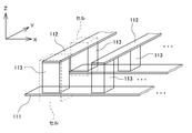
- FIG. 9 is an explanatory diagram illustrating a schematic example of a configuration of a resistance change type memory element used by the machine learning device according to the embodiment of the present invention.
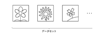
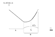
- FIG. 7 is an explanatory diagram illustrating an example of a change in conductance with time in a resistance change type memory element used by the machine learning device according to the embodiment of the present invention. It is explanatory drawing showing the example of the data set for learning input into the machine learning device which concerns on embodiment of this invention.
- the machine learning device includes a storage unit 11, an information input unit 12, a learning processing unit 13, and an output unit 14.
- the storage unit 11 is configured to include a resistance change type memory 11m, and holds the neural network connection weight information as neural network information.
- the neural network of the example of the present embodiment includes an input layer, one hidden layer, and an output layer, as shown in the outline of FIG.
- the input layer and the output layer each have N nodes (N is a natural number of 2 or more) I1, I2,... IN, O1, O2,... ON, and the hidden layer has a number of nodes H1, H2... , HM.
- the connection weight between the j-th node Ij of the input layer and the i-th node Hi of the hidden layer is Wi,j.
- the connection weight between the i-th node Hi of the hidden layer and the j-th node Oj of the output layer is Wj,i.
- the connection weight with the j-th node Oj in the output layer is the transposed matrix W T of the matrix W.
- the resistance change type memory 11m of the present embodiment which holds the information of the connection weight of the neural network, has a plurality of lower electrode lines 111 and a plurality of upper electrode lines as shown in the schematic configuration of FIG. 112 and a resistance change layer 113.
- the resistance change layer 113 is shown as a schematic outer shape thereof, and the inside is transparently shown.
- the plurality of lower electrode lines 111 are parallel to each other in the plane (the normal direction of this plane is the Z axis) and are parallel to each other (hereinafter, the longitudinal direction of the lower electrode lines 111 is the X axis direction). It is arranged with. Further, the plurality of upper electrode lines 112 are arranged in parallel with each other at a predetermined interval in a plane substantially parallel to (not intersecting with) the surface on which the lower electrode lines 111 are arranged.
- the longitudinal direction of the upper electrode line 112 is a direction intersecting with the X axis, and here, as an example, the longitudinal direction of the upper electrode line 112 is arranged in the Y axis direction orthogonal to the X axis, so-called crossbar structure. It is assumed that
- the distance between the surface on which the lower electrode line 111 is arranged and the surface on which the upper electrode line 112 is arranged is about 50 nm or less, preferably 10 nm or less.
- Each electrode line is made of a metal material, and Pt, Cu, Au, Ti, Ag, or the like is preferably used.
- the resistance change layer 113 is disposed between the lower electrode line 111 and the upper electrode line 112.
- the resistance change layer 113 includes a material whose resistance value changes according to an applied voltage (and therefore its conductance also changes).
- a material as a solid electrolyte, for example, a metal sulfide material (Ag 2 S, Cu 2 S, etc.) such as Ag, Cu, Li, Na, Mg, Fe, Ni, Ta, or Zr, or an oxide material.
- the location where the upper electrode line 112 and the lower electrode line 111 intersect in a plan view is a memory cell, and by controlling the voltage applied between the upper electrode line 112 and the lower electrode line 111 in this memory cell.
- the value held by the memory cell (hereinafter referred to as a holding value.
- This holding value is a real value.
- the maximum holding value that can be held is "1" and the minimum holding value is "0”.
- Change (described as normalized) (write data) or maintain the held value.
- the control is performed at time 0.
- the conductance corresponding to the retention value decays more quickly and approaches “0” as compared with the growth over time, and the initial retention value was “1”. Even at this time, when the time Tr elapses after the voltage becomes lower than the potential difference Vth, the stored holding value becomes "0".
- the hold value before applying the voltage V is maintained. Further, if the applied voltage V is controlled so as to exceed the above predetermined range from the predetermined potential difference Vth and become V0+ ⁇ V or more (V0+ ⁇ V>Vth′), as shown in FIG. Becomes exponentially close to the maximum value with the passage of time, and even if the initial holding value is "0", the holding value is "1" when the time Ts elapses after the voltage becomes the potential difference V0+ ⁇ V or more. Becomes
- the phenomenon in which the conductance changes according to the applied voltage in this way is that V0+ ⁇ V or more between the upper electrode line 112 and the lower electrode line 111 in the resistance change layer between the upper electrode line 112 and the lower electrode line 111.
- the metal is deposited from the lower electrode line 111 side and grows as a metal filament to reduce the resistance value of the resistance change layer (conductance increases), while the upper electrode line 112 and the lower electrode line
- the metal filament is ionized again and the resistance value of the resistance change layer increases (conductance decreases).
- the resistance change type memory 11m of the storage unit 11 may be separately provided with a selection line for selecting each memory cell. Since a method of writing/reading data to/from such a resistance change type memory 11m is widely known, its description is omitted here for simplicity.
- the voltage applied to the resistance-change memory 11m according to this example is about 1 mV to 1 V at most, and is generally about 10 to 500 mV, so that its power consumption is relatively low.
- the resistance change type memory having the so-called crossbar type structure as described above can be manufactured by using a well-known fine processing technique.
- the present embodiment is not limited to this example, and the first electrode line, the first resistance change layer, the second electrode line, the second resistance change layer, and the third electrode line are arranged in this order. You may use what laminated.
- a voltage is applied between the first electrode line and the second electrode line, or a voltage is applied between the second electrode line and the third electrode line.
- a new metal filament grows on one electrode line side of the first electrode line and the third electrode line, and the other metal filament contracts. It is an atomic switch that operates in a so-called tug of war type.
- connection weight Wi,j,+ and the negative connection weight Wi,j are respectively determined by the resistance value of the first resistance change layer and the resistance value of the second resistance change layer.
- the information input unit 12 generates input data to be input to the neural network.
- both the input data to the neural network and the output data of the neural network are vector data, and include a plurality of data elements corresponding to the respective nodes of the input layer and the output layer.
- the information input unit 12 arranges pixel values of pixels of the binary image data in a predetermined order (raster scan order may be used) as input data, and outputs a plurality of values.
- Vector data including the data elements of.
- the learning processing unit 13 is configured by a logic circuit or the like, and stores information using information input from the information input unit 12 at the time of learning (whether learning or inference is to be instructed from the outside).
- the information on the connection weight of the neural network stored in the unit 11 is updated.
- the voltage V0 is constantly applied to each memory cell of the resistance change type memory 11m.
- the voltage V0 is a voltage (Vth ⁇ V0 ⁇ Vth') sufficient to maintain the value held by the memory cell.
- the voltage V0 that is constantly applied does not have to be constant, and for each memory cell, the growth state of the metal filament at the time of applying the voltage to the memory cell (that is, the resistance value of the memory cell). ), it may be controlled to change. Specifically, when the resistance value of the memory cell is smaller (the more the metal filament is growing), the smaller the value of V0 is, the more the growth rate of the metal filament per unit time is changed to the growth state at that time. It can be made substantially uniform regardless of.
- the update of the connection weight information is performed as follows.
- the learning processing unit 13 initially initializes the information of the connection weight by a predetermined method. Since various widely known methods such as Xavier's method can be adopted as this initialization method, detailed description thereof is omitted here.
- the learning processing unit 13 sequentially receives a plurality of input data included in the data set prepared for learning from the information input unit 12, and inputs each input data to the neural network stored in the storage unit 11. The output data of the neural network at that time is calculated.
- both the input data and the output data are binary (binary) in which each data element is “0” or “1” (the values Ij, Oj of each node are Ij, Oj ⁇ 0, 1 ⁇ ).
- ⁇ j means summing about j
- b is a predetermined bias value (scalar value).
- the function f(X) is a binarization function that becomes “1” when X>0 and otherwise becomes “0” (same in the following description).
- ⁇ i means that i is summed.
- Other parts are the same as those used for the calculation of the hidden layer node (the bias value may be the same as or different from the value when calculating the hidden layer).
- the learning processing unit 13 is a resistance change type that holds information of the connection weight related to the calculation of the data element that does not reach the target value (the value of the corresponding data element of the teacher data) among the data elements of the output data. Control is performed so as to apply an electrical signal that causes the memory cell of the memory 11m to approach a target value, and the held value of the memory cell is updated.
- the neural network is an auto encoder, and in this case, since the input data is the teacher data, the target value of each data element of the output data is the same as the value of the corresponding data element of the input data. Become.
- the voltage applied to the memory cell of the resistance-change memory 11m is increased from the constantly applied voltage V0 by ⁇ V for a predetermined time ⁇ T (hereinafter, ⁇ T>Ts and ⁇ T>Tr). , So that a pulsed voltage having a potential of V0+ ⁇ V is applied to the memory cell. At this time, the voltage applied to the memory cell of the resistance change type memory 11m holding the value of Wi,j,- is controlled to fall below Vth for a predetermined time ⁇ T.
- the applied voltage is increased by ⁇ V from the constantly applied voltage V0 for a predetermined time ⁇ T, and a pulsed voltage having a potential of V0+ ⁇ V is applied to the memory cell.
- the voltage applied to the memory cell of the resistance change type memory 11m that holds the value of Wi,j,+ is controlled to fall below Vth for the time of ⁇ T.
- the calculation of the value of each node of the hidden layer and the output layer can be realized by using a logic circuit, an adder, and a comparator circuit (the function f can be realized by a comparator circuit that compares with the value “0”). Also in the learning process, the comparison of the values of each node can be performed by using an AND circuit or the like, the conditional branch can be realized by an AND circuit or an OR circuit, and the voltage control is performed by a general voltage control. It can be realized by a circuit. That is, the learning processing unit 13 can be realized by a relatively simple circuit that does not necessarily require a processor or the like that is a program execution module.
- the processing can be realized by comparatively simple comparison and conditional branching, so that the program is simple and has a low processing load.
- the output unit 14 is composed of a logic circuit or the like, and performs inference using information input from the information input unit 12 and information of the connection weight of the neural network stored in the storage unit 11 at the time of inference.
- the output unit 14 generates output data from the value of each node of the output layer obtained here and outputs it as a result of inference. For example, when image data is obtained as a result of inference, the value of each data element of output data is set as a predetermined pixel value of planar image data of a predetermined size (when input data is image data, the same size may be used). Image data is arranged in order (raster scan order is acceptable).
- the machine learning device basically has the above configuration and operates as follows. In the following example, an example of learning grayscale image data as illustrated in FIG. 5 will be described.
- the learning processing unit 13 of the machine learning device receives the instruction to start the learning process (the instruction to initialize and start), and starts the process illustrated in FIG. 6A.
- the learning processing unit 13 first initializes the connection weight of the neural network illustrated in FIG. 2 (S1).
- the initial value of each of the number of nodes in the layer and the output layer, M is the number of nodes in the hidden layer) is determined, and if the initial value is set to "0", the memory cell of the storage unit 11 that holds the determined connection weight ( Control is performed so that a voltage lower than the potential V0 is applied to the memory cells that retain the respective values of the coupling weights Wi,j,+, Wi,j,-) for a sufficient time so that the retained value becomes "0". To do. As a result, the metal filaments in the corresponding memory cells become ionized (or remain in that state), and the holding value of these memory cells is set to "0".
- the learning processing unit 13 exceeds V0+ ⁇ V in the memory cell of the storage unit 11 that holds the positive value Wi,j,+ of the connection weight determined to be “1” among the connection weights whose initial values are determined.
- a voltage is applied to the memory cell of the storage unit 11 that holds the negative value Wi,j,- so that a voltage lower than the potential V0 is applied.
- the application time of this voltage is set to be sufficient for at least the holding value of the memory cell holding the positive value Wi,j,+ to be "1". By doing so, the metal filament grows in the memory cell of the storage unit 11 that holds the positive value Wi,j,+, and the held value of the memory cell increases to “1”.
- the learning processing unit 13 further applies the potential V0 to the memory cell of the storage unit 11 that holds the positive value Wi,j,+ of the connection weight determined to be “ ⁇ 1” among the connection weights whose initial values are determined.
- a voltage lower than V0+ ⁇ V is applied to the memory cell of the storage unit 11 that holds the negative value Wi,j, ⁇ .
- the application time of this voltage is set to be sufficient for at least the holding value of the memory cell holding the negative value Wi,j,- to be "1". In this way, the metal filament in the memory cell of the storage unit 11 that holds the positive value Wi,j,+ is in the ionized state (or the state is maintained), and this memory cell is held. The value decreases to "0".
- the learning processing unit 13 starts the machine learning processing shown in FIG. 7 (S2).
- a plurality of gray scale image data as illustrated in FIG. 5 are prepared as a data set as input data to be input to the neural network.
- the learning processing unit 13 accepts the vector data generated by the information input unit 12 for each grayscale image data and sequentially selects the vector data (S11).
- the learning processing unit 13 inputs the selected vector data to the neural network and calculates output data of the neural network (S12).
- Wj,i is the element at the j-th row and the i-th column of the transposed matrix [Wi,j] T of the matrix [Wi,j] having Wi,j as an element.
- the control for increasing the value of Wi,j,+ or Wi,j,- is performed by previously changing the voltage applied to the memory cell holding the value to be increased as a holding value. This is performed by raising the voltage V0 which is constantly applied by ⁇ V for a predetermined time ⁇ Tp and controlling so as to apply a voltage having a potential of V0+ ⁇ V>Vth' to the memory cell.
- the value to be reduced is applied to the memory cell holding the value.
- the voltage is set to a voltage lower than the potential difference Vth for a predetermined time ⁇ Tm.
- time ⁇ Tp for increasing the hold value and the time ⁇ Tm for decreasing the hold value may be different from each other.
- These times ⁇ Tp and ⁇ Tm may be, for example, times sufficient to set the holding values to “1” and “0”, respectively. Further, these times ⁇ Tp and ⁇ Tm may be only times sufficient to increase the holding value from “0” by a predetermined value or decrease the holding value from “1” by a predetermined value, respectively.
- the learning processing unit 13 repeats the processing of the processing S17, S18, or S19 for the number of data elements Oj extracted in the processing S13, and further repeats the processing of the processing S15 and subsequent times for the number of hidden layer nodes. If the value of Hi is "0" in the process S15 (S15: No), the learning processing unit 13 continues the repetitive process without performing the processes of the processes S16 to S19 (next hidden layer). The processing of step S15 and the subsequent steps is executed for the node (1).
- the learning processing unit 13 returns to the processing S11, and if there is vector data to be input next, repeats the processing from the processing S12 onward for the vector data. If there is no vector data to be input next (if all the accepted vector data have been processed), the machine learning process of FIG. 7 ends.
- the processing of the learning processing unit 13 illustrated in FIGS. 6A and 7 can also be realized by using a microcomputer or the like. Also in this case, the processing performed by the microcomputer is only binary comparison processing, repetitive processing, and voltage control processing, so the processing load is higher than that in the case of performing general back propagation processing. Has been reduced.
- the learning processing unit 13 can also be realized as hardware using a logic circuit, as described above.
- various widely known methods such as a method using a circuit such as a multiplexer and a clock circuit can be adopted as a method for realizing the sequential selection operation as exemplified in the processes S14 and S16.
- the learning processing method the value of each node of the input layer and the output layer and the value of each node of the hidden layer are referred to, but the present embodiment is not limited to this, and it is simpler.
- the learning process may be performed by referring only to the value of each node of the input layer and the output layer without referring to the value of the node of the hidden layer.
- the learning processing unit 13 stores the memory of the resistance change type memory 11m that holds the information of the connection weight related to the calculation of the data element that does not reach the target value in the output data.
- the same operation as in the above-described example is performed in the point that control is performed so that an electric signal that brings the cell closer to the target value is applied, but the specific processing content is different.
- the voltage applied to the 11 m memory cell is increased by ⁇ V from the constantly applied voltage V0 for a predetermined time ⁇ Tp, and the voltage of V0+ ⁇ V is applied to the memory cell.
- the voltage applied to the memory cell of the resistance change type memory 11m holding the value of Wi,j,+ is controlled so as to fall below Vth for the time of ⁇ Tm.
- the comparison of the value of each node can be performed by using an AND circuit or the like
- the conditional branch can be realized by an AND circuit or an OR circuit
- the voltage control can be performed by a general method. It can be realized by a voltage control circuit. That is, the learning processing unit 13 can be realized by a relatively simple circuit that does not necessarily require a processor or the like that is a program execution module. Further, even when the program execution module is used, the processing can be realized by comparatively simple comparison and conditional branching, so that the program is simple and has a low processing load. As described above, according to the present embodiment, it is possible to perform learning with a small-scale hardware and expand the use cases of the neural network.
- the potential V0 that is constantly applied to the memory cell of the resistance change type memory 11m of the storage unit 11 is set to a value that is lower than the potential Vth by a predetermined potential Vm, and the filament is attenuated with time. You may let it be used. By doing so, it becomes possible to use the learning content as a memory that attenuates over time, and a natural forgetting process can be realized.
- the forgetting speed can also be controlled (decreasing Vm slows the forgetting speed because damping is less likely to occur, and increasing Vm speeds up the forgetting speed because the damping progresses quickly).
- the learning processing unit 13 may repeat the learning process using one data set a plurality of times. That is, in the example of the present embodiment, the learning processing unit 13 starts a loop after initializing (S1) the connection weights of the neural network illustrated in FIG. 2 as illustrated in FIG. 6B. (S3), the machine learning process shown in FIG. 7 is executed (S2). Then, every time the machine learning process of FIG. 7 is completed, it is checked whether or not the loop termination condition is satisfied (for example, the machine learning process is executed a predetermined number of times) (S4). When the machine learning process is not performed and the loop termination condition is not satisfied, the process returns to the process S2 to repeat the process.
- the machine learning process is performed a predetermined number of times, the process related to machine learning is terminated. In this case, in the machine learning process of the process S2, the machine learning process using the same data set is performed for each repetition.
- the time interval for updating the value held by each memory cell (controlling the voltage applied to the memory cell) is constantly applied to the memory cell.
- the potential Vm is set to be shorter than the time Tr required for the conductance of the memory cell to decay from the maximum state to the minimum state when the voltage V0 is applied, or the learning process is performed. May be.
- next learning is performed in a state where the metal filament of the memory cell is not attenuated and remains, so that, for example, as shown in FIG. 8, for example, a memory that initially retains a value of “1”.
- the cell memory cell in which the metal filament grows sufficiently and the conductance is sufficiently large
- the voltage V0 is When applied, the conductance gradually decreases (A).
- the voltage V0+ ⁇ V sufficient to grow the metal filament of this memory cell is increased so that the holding value increases.
- the metal filament grows again for a period of ⁇ Tp in the decaying state (state in which the conductance representing the holding value is not “0”), and the holding value increases (B). ..
- the state of the memory cell is stochastically controlled to update the information of the connection weight of the neural network, and the input data contains noise. It is possible to prevent over-learning etc.
- the holding value held by the resistance change type memory 11m of the storage unit 11 is assumed to be maintained at “0” or “1” when no voltage is applied.
- the resistance change memory that realizes the storage unit 11 used in the present embodiment is not limited to the resistance change memory of this example.
- the resistance change type memory 11m that realizes the storage unit 11 of the machine learning device according to another example of the present embodiment has a lower electrode line 111 and an upper electrode line 112 as illustrated in the structure of FIG.
- a plurality of resistance holding layers 114a, 114b arranged in parallel to the lower electrode line 111 and the upper electrode line 112 (and thus in parallel with each other) in the resistance change layer 113 between ...With n.
- the lower electrode line 111 and the upper electrode line 112 are arranged in parallel in different planes (the normal direction of this plane is the Z axis) in parallel, and the lower electrode line 111 and the upper electrode line 112 are arranged.
- the respective angles in the longitudinal direction of and are arranged so as to intersect each other in a plan view.
- the longitudinal direction of the lower electrode line 111 is arranged in the X-axis direction
- the longitudinal direction of the upper electrode line 112 is arranged in the Y-axis direction orthogonal to the X-axis direction (that is, also in the cross direction here). It has a bar structure).
- the resistance holding layer 114 is formed using the same material as the metal of the metal filament deposited in the resistance change layer 113.
- the resistance holding layer 114 corresponds to the pseudo electrode of the present invention. Further, it is assumed that the resistance holding layer 114 has such a size that it is included in the resistance change layer 113 included in one memory cell in a plan view (FIG. 10).
- the value held by the memory cell changes as follows.
- the resistance holding layer 114a closest to the lower electrode line 111 is referred to as a first resistance holding layer 114a
- the resistance holding layers 114b, c... n is referred to as a second resistance holding layer 114b, a third resistance holding layer 114c...
- the metal filament when the metal filament is initially grown from the end of the resistance change layer 113 on the lower electrode line 111 side (hereinafter referred to as the lower end) to the kth resistance holding layer 114k, the upper electrode line 112 is formed. If the voltage applied between the lower electrode line 111 and the lower electrode line 111 is controlled to fall below a predetermined potential difference Vth, the conductance is attenuated more quickly than growth over time, as in the example shown in FIG. After a lapse of a predetermined time (time Tr), the metal filament is grown from the lower end to the (k-1)th resistance holding layer 114(k-1).
- the voltage applied between the upper electrode line 112 and the lower electrode line 111 is controlled to be within a predetermined range from the predetermined potential Vth (exceeding Vth to Vth+Vth′). Then, the metal filament does not grow or decay, and at that time, the metal filament has grown from the end of the resistance change layer 113 on the lower electrode line 111 side (hereinafter, referred to as the lower end) to the kth resistance holding layer 114k. If that happens, that condition is maintained.
- the control of the applied voltage is referred to as "maintenance control”.
- the potential difference between the upper electrode line 112 and the lower electrode line 111 is controlled to be lower than Vth. Also, the growth state from the lower end to the resistance holding layer 114 (the resistance holding layer on the side close to the nearest lower electrode line 111) which is in contact with the metal filament at that time is maintained. That is, the resistance holding layer 114 controls the attenuation of the metal filament.
- the applied voltage may be controlled to be temporarily the reset voltage (for example, -(V0+ ⁇ V)) before performing the attenuation control. Good. The reset voltage may not be applied during the learning process.
- the upper electrode line 112 and the lower electrode line 111 are connected to each other.
- the voltage V applied during the period exceeds a predetermined potential difference Vth and becomes V0+ ⁇ V or more (V0+ ⁇ V>Vth′)
- the conductance exponentially increases with time as illustrated in FIG. 4B.
- the conductance further increases exponentially with time, and a predetermined time ( After the lapse of time Ts, the metal filament is grown from the lower end to the (k+2)th resistance holding layer 114(k+2).
- the control of the applied voltage is referred to as “growth control”.
- the memory cell including the resistance change layer 113 can hold multi-valued information by itself without applying a voltage.
- the holding value representing the maximum conductance value is normalized to "1" and the holding value representing the minimum conductance value is standardized to "0".
- the learning processing unit 13 When using the resistance change type memory 11m capable of holding such multi-valued information, the learning processing unit 13 operates as follows.
- the learning processing unit 13 in this example sequentially receives a plurality of input data prepared for learning from the information input unit 12, and inputs the respective input data to the neural network stored in the storage unit 11. , The output data of the neural network is calculated.
- both the input data and the output data are binary (binary) in which each data element is “0” or “1” (the values Ij, Oj of each node are Ij, Oj ⁇ . ⁇ 0,1 ⁇ ).
- ⁇ j means summing about j
- b is a predetermined bias value (scalar value).
- the function f(X) is a binarization function that becomes “1” when X>0 and becomes “0” otherwise, as described above.
- multivalued information any value of 0, G, 2G,..., nG, where n is a positive integer
- nG is held in each memory cell of the resistance change type memory. Therefore, it is possible to represent multi-valued values from ⁇ nG to +nG (where ⁇ 1 ⁇ nG ⁇ 0 ⁇ nG ⁇ 1).
- ⁇ i means that i is summed.
- the other parts are the same as those used for the calculation of the hidden layer node (the bias value may be the same as or different from the value when calculating the hidden layer).
- the learning processing unit 13 approaches the target value with respect to the memory cell of the resistance change type memory 11m that holds the information of the coupling weight related to the calculation of the data element that does not reach the target value in the output data.
- the control is performed so as to apply an electric signal. If the neural network is an auto encoder, the target value of each data element of the output data will be the value of the corresponding data element of the input data.
- the voltage applied to the memory cell of the resistance-change memory 11m is increased from the constantly applied voltage V0 by ⁇ V for a predetermined time ⁇ Tp (hereinafter, ⁇ T>Ts and ⁇ T>Tr). , So that a voltage having a potential of V0+ ⁇ V is applied to the memory cell (growth control).
- the learning processing unit 13 controls the voltage applied to the memory cell of the resistance change type memory 11m holding the value of Wi,j,- so as to fall below Vth for a predetermined time ⁇ Tm (attenuation control).
- ⁇ Tp and ⁇ Tm are determined in the same manner as in the example already described (the same applies below).
- the voltage to be applied is increased by ⁇ V from the voltage V0 which is constantly applied for a predetermined time ⁇ Tp, and the voltage of V0+ ⁇ V is applied to the memory cell (growth control).
- the learning processing unit 13 controls the voltage applied to the memory cell of the resistance change type memory 11m that holds the value of Wi,j,+ so as to fall below Vth for a time of ⁇ Tm (attenuation control).
- the voltage applied to the memory cell of the resistance-change memory 11m that holds is maintained at V0 (maintenance control).
- the learning processing unit 13 instead of the learning processing unit 13 referring to the values of the nodes in the input layer and the output layer and the values of the nodes in the hidden layer, the values of the nodes in the hidden layer are more simply referred to. Instead, the learning process may be performed by referring to only the values of the nodes in the input layer and the output layer.
- the learning processing unit 13 using a memory cell that holds information on multi-valued connection weights, when inputting each input data to the neural network stored in the storage unit 11, The same operation as described above is performed until the process of calculating the output data of the network.
- the learning processing unit 13 determines that the value of the j-th data element of the output data (the value of the node Oj) is not equal to the value of the corresponding j-th data element of the input data (the value of the node Ij) (Oj ⁇ ).
- the voltage applied to the 11 m memory cell is increased by ⁇ V from the constantly applied voltage V0 for a predetermined time ⁇ Tp, and the voltage of V0+ ⁇ V is applied to the memory cell (growth control ).
- the voltage applied to the memory cell of the resistance change type memory 11m that holds the value of Wi,j,+ is controlled to fall below Vth for the time of ⁇ Tm (attenuation control).
- the voltage applied to the memory cell of the resistance-change memory 11m that holds the voltage is maintained at V0 (maintenance control).
- the comparison of the values of each node can be performed by using an AND circuit or the like
- the conditional branch can be realized by an AND circuit or an OR circuit
- the voltage control is generally performed.
- the potential V0 during the maintenance control is set to a value lower than Vth by a predetermined potential Vm, and the filament is temporally changed. It may be used after being attenuated. In this way, the learning content is attenuated over time, and a natural forgetting process can be realized.
- the time interval for updating the value held by each memory cell is The potential Vm is set so that it becomes shorter than the time Tr required for the conductance of the memory cell to decay from the maximum state to the minimum state when a voltage V0 that is constantly applied is applied. , Learning processing may be performed.
- the number of memory cells whose values have been changed is counted, and when the count value falls below a predetermined threshold, the content of learning The machine learning process may be repeated as if the values have converged.
- the machine learning device may be one in which the storage unit 11, the information input unit 12, the learning processing unit 13, and the output unit 14 are packaged as one chip. Since the learning processing unit 13 is composed of a relatively simple circuit such as a logic circuit as already described, the circuit does not become large even if these are packaged as one chip.
- the output unit 14 performs the inference process in the same manner as the learning processing unit 13 generates the value of each node in the output layer. Then, the output unit 14 outputs the vector data in which the values of the respective nodes of the output layer are arranged as the result of the inference.
Landscapes
- Engineering & Computer Science (AREA)
- Physics & Mathematics (AREA)
- Health & Medical Sciences (AREA)
- Life Sciences & Earth Sciences (AREA)
- Biomedical Technology (AREA)
- Biophysics (AREA)
- Theoretical Computer Science (AREA)
- Evolutionary Computation (AREA)
- Computational Linguistics (AREA)
- Data Mining & Analysis (AREA)
- Artificial Intelligence (AREA)
- General Health & Medical Sciences (AREA)
- Molecular Biology (AREA)
- Computing Systems (AREA)
- General Engineering & Computer Science (AREA)
- General Physics & Mathematics (AREA)
- Mathematical Physics (AREA)
- Software Systems (AREA)
- Neurology (AREA)
- Semiconductor Memories (AREA)
Abstract
入力層と隠れ層と出力層とを含むニューラルネットワークの層間の結合重みの情報を抵抗変化型メモリ素子により保持する機械学習デバイスであって、複数のデータ要素を含む入力データを受け入れ、ニューラルネットワークの結合重みの情報を用いて、複数のデータ要素を含む出力データを演算し、学習中は、当該出力データのうち、目的の値に達していないデータ要素の演算に係る結合重みの情報を保持する抵抗変化型メモリ素子に対し、目的の値に近接させる電気的信号を印加する学習処理を実行する。
Description
本発明は、機械学習デバイス及びその制御方法に関する。
近年、ニューラルネットワーク等の機械学習装置が広く開発され、組合せ最適化問題および意思決定問題等の最適化問題の解の探索をはじめ、機械制御等の分野に至るまで、種々の応用研究も行われている。
一例として特許文献1には、最適解探索問題の解を量子ドットからなるナノスケールの回路を利用して探索する量子ドットによる解探索システムが開示されている。また、特許文献2には、フィードバック制御を行って高速かつ効率的に充足可能性問題(Satisfiability Problem, SAT)を解くことが可能な解探索システムが開示されている。
また一方、ニューラルネットワークに対する応用を念頭に、抵抗変化型メモリ素子の研究を行っている例もある。
しかしながら、上記従来例の技術では、ニューラルネットワークの各層の結合重みの学習過程は、いわゆるバックプロパゲーションの処理により行われるため、演算が比較的複雑なものとなり、GPU(Graphics Processing Unit)等、ベクトルや行列演算に適したハードウェアを用いているのが現状である。このために現実には、ニューラルネットワークの応用可能な現場は制限されており、学習処理のためのハードウェアを設置できる場所か、当該ハードウェアとの間で通信が可能な場所でなければならない。
本発明は上記実情に鑑みて為されたもので、学習処理の負荷を軽減して小規模なハードウェアによる学習を可能とし、ニューラルネットワークの利用場面を拡大できる機械学習デバイス、及びその制御方法を提供することを、その目的の一つとする。
上記従来例の問題点を解決する本発明の一態様は、入力層と隠れ層と出力層とを含むニューラルネットワークの層間の結合重みの情報を抵抗変化型メモリ素子により保持する機械学習デバイスであって、複数のデータ要素を含む入力データを受け入れ、前記ニューラルネットワークの前記結合重みの情報を用いて、複数のデータ要素を含む出力データを演算する演算手段と、学習中は、前記出力データのうち、目的の値に達していないデータ要素の演算に係る前記結合重みの情報を保持する抵抗変化型メモリ素子に対し、目的の値に近接させる電気的信号を印加する学習処理を実行する学習手段と、を含むこととしたものである。
本発明によれば、基本的に、目的の値に達しているか否かという判断で学習処理を行うため、その負荷を軽減して小規模なハードウェアによる学習を可能とし、ニューラルネットワークの利用場面を拡大できる。
以下、本発明の実施の形態に係る機械学習デバイスについて、図面を参照しながら説明する。本実施の形態の機械学習デバイスは、図1に例示するように、記憶部11と、情報入力部12と、学習処理部13と、出力部14とを含んで構成されている。
記憶部11は、抵抗変化型メモリ11mを含んで構成され、ニューラルネットワークの情報として、ニューラルネットワークの結合重みの情報を保持する。
本実施の形態の例のニューラルネットワークは、図2にその概要を例示するように、入力層と、1層の隠れ層と、出力層とを含む。入力層と出力層とはいずれもN個(Nは2以上の自然数)のノードI1,I2,…IN、O1,O2,…ONを備え、隠れ層はNより少ない数のノードH1,H2…,HMを備えている。また、入力層のj番目のノードIjと隠れ層のi番目のノードHiとの間の結合重みをWi,jとする。また隠れ層のi番目のノードHiと、出力層のj番目のノードOjとの間の結合重みを、Wj,iとする。
つまり、入力層のj番目のノードIjと隠れ層のi番目のノードHiとの間の結合重みWをW=[Wi,j]と行列で表現すると、隠れ層のi番目のノードHiと、出力層のj番目のノードOjとの間の結合重みは行列Wの転置行列WTとなっている。
また、このニューラルネットワークの結合重みの情報を保持する、本実施の形態の抵抗変化型メモリ11mは、図3にその概略構成を示すように、複数の下部電極ライン111と、複数の上部電極ライン112と、抵抗変化層113とを含んで構成される。なお、図3では、図示の都合上、抵抗変化層113をその概略の外形として示し、内部を透過して示している。
ここで複数の下部電極ライン111は、平面内(この平面の法線方向をZ軸とする)に互いに平行に(以下、この下部電極ライン111の長手方向をX軸方向とする)所定の間隔をおいて配されている。また複数の上部電極ライン112は、下部電極ライン111が配されている面と実質的に平行な(交わらない)面内に、互いに平行に、所定の間隔をおいて配される。この上部電極ライン112の長手方向はX軸に対して交わる方向となっており、ここでは一例としてX軸に直交するY軸方向に上部電極ライン112の長手方向が配されて、いわゆるクロスバー構造をなしているものとする。
ここで下部電極ライン111が配される面と、上部電極ライン112が配される面との間隔は50nm程度以下、好ましくは10nm以下となっている。また各電極ラインは金属材料で構成され、例えば、Pt、Cu,Au,Ti、Ag等が好適に使用される。
また少なくとも、上部電極ライン112と下部電極ライン111とが平面視で交差している箇所(個々の抵抗変化型メモリ素子を構成し、メモリセルとなる箇所、図3中では破線で示す)においては下部電極ライン111と上部電極ライン112との間に、抵抗変化層113が配される。この抵抗変化層113は、印加電圧によって抵抗値を変化させる(従ってそのコンダクタンスも変化する)材料を含んでなる。このような材料としては固体電解質として、例えばAg,Cu,Li,Na,Mg,Fe,Ni,Ta,Zrなどといった金属の硫化物材料(Ag2S,Cu2S等)や、酸化物材料(Ta2O5,ZrO2)、あるいは上記金属のイオン(1価のAg,Cu,Li,Na,Mgの各イオンや、2価のFe,Niのイオン等)を含むポリエチレンオキシドなどの高分子系材料がある。
上部電極ライン112と下部電極ライン111とが平面視で交差している箇所は、メモリセルとなり、このメモリセルにおいて上部電極ライン112と下部電極ライン111との間に印加する電圧を制御することで、当該メモリセルが保持する値(以下、保持値と呼ぶ。この保持値は実数値となる。以下の説明では保持可能な最大の保持値を「1」、最小の保持値を「0」と規格化したものとして説明する)を変化させ(データの書き込みを行い)、あるいはその保持値を維持させる。
このため本実施の形態では、メモリセルにおいて上部電極ライン112と下部電極ライン111との間に印加する電圧が所定の電位差Vthを下回るように印加電圧を制御すると(図4では時刻0において制御を行うと)、図4(a)に示すように、保持値に相当するコンダクタンスは時間経過とともに成長に比べると迅速に減衰して「0」に近づき、当初の保持値が「1」であったときでも、上記電圧が上記電位差Vthを下回ることとなってから時刻Trが経過したときには記憶している保持値は「0」となる。
また印加する電圧Vが所定の電位差Vthを超えて、このVthから所定の範囲(Vth<V<Vth′)であるよう制御すると、電圧Vを印加する前の保持値が維持される。さらに印加する電圧Vを、この所定の電位差Vthから上記所定の範囲を超え、V0+ΔV以上となる(V0+ΔV>Vth′)よう制御すると、図4(b)に例示するように、保持値であるコンダクタンスは時間経過とともに指数関数的に最大値に近づき、当初の保持値が「0」であっても、上記電圧が上記電位差V0+ΔV以上となってから時間Tsが経過したときには、保持値は「1」となる。
このように印加電圧に応じてコンダクタンスが変化する現象は、上部電極ライン112と下部電極ライン111との間にある抵抗変化層において、上部電極ライン112と下部電極ライン111との間に上記V0+ΔV以上の電圧が印加されると、下部電極ライン111側から金属が析出して金属フィラメントとして成長して抵抗変化層の抵抗値が減少し(コンダクタンスは上昇し)、一方、上部電極ライン112と下部電極ライン111との間の電位差がVthを下回ると金属フィラメントが再度イオン化して抵抗変化層の抵抗値が上昇する(コンダクタンスは低下する)ことから生じると考えられる。
なお、抵抗変化層の材質によっては、金属フィラメントが抵抗変化層の下部電極ライン111側の端から上部電極ライン112側の端まで成長すると、上部電極ライン112と下部電極ライン111との間の電位差がVthを下回っても金属フィラメントの再イオン化が生じず、抵抗変化層の抵抗値が維持されるものがある。この場合は、再イオン化のために、保持値を「0」とするべく、一時的にリセット電圧(例えば-(V0+ΔV))を印加して再イオン化を促す。
この記憶部11の抵抗変化型メモリ11mには、各メモリセルを選択する選択ラインが別途設けられていてもよい。またこのような抵抗変化型メモリ11mに対してデータを書き込み・読み出しを行う方法は広く知られているので、ここでは簡単のために、その説明を省略する。
なお、この例に係る抵抗変化型メモリ11mに対する印加電圧は、1mVから高々1Vほどであり、一般的には10~500mV程度であるため、その消費電力は比較的低く抑えられている。また上述のような、いわゆるクロスバー型の構造を有する抵抗変化型メモリは、広く知られている微細加工技術を用いて製造できる。
また本実施の形態の一例では、一対のメモリセルにより、一つの結合重みの情報が保持されるものとする。すなわち、本実施の形態の例では、一つの結合重みの情報Wi,jは、正の結合重みWi,j,+と負の結合重みWi,j,-との2つの値の差Wi,j=(Wi,j,+)-(Wi,j,-)として表され、一つのメモリセルは、いずれかの結合重みの情報に係る、正の結合重みまたは負の結合重みの一方の値を保持値として保持する。これにより抵抗変化型メモリの各メモリセルにおいて保持値を二値化して用いる場合であっても、正の値と負の値とを含む多値の表現が可能となる。
もっとも、本実施の形態はこの例に限られるものではなく、第1の電極ライン、第1の抵抗変化層、第2の電極ライン、第2の抵抗変化層、第3の電極ラインをこの順に積層したものを用いてもよい。この例の抵抗変化型メモリ11mを用いると、第1の電極ラインと第2の電極ラインとの間に電圧を印加するか、あるいは第2の電極ラインと第3の電極ラインとの間に電圧を印加するかにより、第2の電極ラインを挟んで、第1の電極ラインと第3の電極ラインのうち一方の電極ライン側に新たな金属フィラメントが成長し、他方の金属フィラメントは収縮する、いわゆる綱引き型の動作をする原子スイッチとなる。この綱引き型の原子スイッチを用いる場合、第1の抵抗変化層の抵抗値と、第2の抵抗変化層の抵抗値とによりそれぞれ正の結合重みWi,j,+と負の結合重みWi,j,-との2つの値を表し、その差Wi,j=(Wi,j,+)-(Wi,j,-)として結合重みの情報Wi,jを表すこととしてもよい。
情報入力部12は、ニューラルネットワークに対して入力する入力データを生成する。具体的に本実施の形態では、ニューラルネットワークへの入力データ及びニューラルネットワークの出力データはいずれもベクトルデータであり、入力層及び出力層の各ノードに対応する、複数のデータ要素を含んでいる。
そこで情報入力部12は、例えば画像データを学習あるいは推論させる場合、入力データとしては、当該2値の画像データの画素の画素値を所定の順序(ラスタスキャン順でよい)で配列して、複数のデータ要素を含むベクトルデータとする。
学習処理部13は、論理回路等により構成され、学習時(学習を行うか推論を行うかは外部から指示されるものとする)に、情報入力部12から入力される情報を用いて、記憶部11に格納したニューラルネットの結合重みの情報を更新する。なお、本実施の形態のここでの例では、抵抗変化型メモリ11mの各メモリセルには、定常的に電圧V0が印加されているものとする。ここでの例では、この電圧V0は、メモリセルが保持している値を維持させるのに十分な電圧(Vth≦V0≦Vth′)であるものとする。
なお、この定常的に印加する電圧V0は、常に一定でなくてもよく、メモリセルごとに、当該メモリセルに電圧を印加する時点での金属フィラメントの成長の状態(すなわち当該メモリセルの抵抗値)に応じて変化するよう制御されてもよい。具体的には、メモリセルの抵抗値が小さいほど(金属フィラメントが成長しているほど)、V0の値を小さくすると、単位時間あたりの金属フィラメントの成長の度合いを、その時点での成長の状態によらず、実質的に均一にできる。
本実施の形態において、この結合重みの情報の更新は次のようにして行われる。学習処理部13は、当初、結合重みの情報を予め定めた方法で初期化する。この初期化の方法はXavierの方法など、広く知られた種々の方法を採用できるので、ここでの詳しい説明は省略する。
そして学習処理部13は、学習用に用意されたデータセットに含まれる、複数の入力データを逐次的に情報入力部12から受け入れ、それぞれの入力データを、記憶部11に格納したニューラルネットワークに入力したときの、当該ニューラルネットワークの出力データを演算する。
具体的に、ここでは入力データ及び出力データはいずれも、各データ要素が「0」または「1」となるバイナリ(2値)である(各ノードの値Ij,Ojが、Ij,Oj∈{0,1}である)とする。このとき学習処理部13は、隠れ層の各ノードHiの値を、記憶部11が保持する保持値に基づいて得られるWi,jを用いて、
Hi=f(Σj Wi,j・Ij+b)
として演算する。ここでΣjは、jについて総和することを意味し、bは予め定められたバイアス値(スカラー値)である。また、関数f(X)は、X>0のとき「1」となり、そうでない場合は「0」となる二値化の関数である(以下の説明において同じ)。
Hi=f(Σj Wi,j・Ij+b)
として演算する。ここでΣjは、jについて総和することを意味し、bは予め定められたバイアス値(スカラー値)である。また、関数f(X)は、X>0のとき「1」となり、そうでない場合は「0」となる二値化の関数である(以下の説明において同じ)。
学習処理部13は、さらに、出力層の各ノードOjの値を、記憶部11が保持する保持値に基づいて得られるWi,jを用いて、
Oj=f(Σi Wj,i・Hi+b)
として演算する。ここでΣiは、iについて総和することを意味する。その他の部分は隠れ層のノードの演算に用いたものと同様である(バイアスの値は隠れ層を演算する際の値と同じであっても、異なっていてもよい)。
Oj=f(Σi Wj,i・Hi+b)
として演算する。ここでΣiは、iについて総和することを意味する。その他の部分は隠れ層のノードの演算に用いたものと同様である(バイアスの値は隠れ層を演算する際の値と同じであっても、異なっていてもよい)。
次に学習処理部13は、出力データのデータ要素のうち、目的の値(教師データの対応するデータ要素の値)に達していないデータ要素の演算に係る結合重みの情報を保持する抵抗変化型メモリ11mのメモリセルに対して、目的の値に近接させる電気的信号を印加するよう制御して、メモリセルの保持値を更新する。本実施の形態の一例では、ニューラルネットワークはオートエンコーダであり、この場合、入力データが教師データとなるので、出力データの各データ要素の目的の値は、入力データの対応するデータ要素の値となる。
具体的にこの学習処理部13は、出力データのj番目のデータ要素の値(ノードOjの値)が、入力データにおいて対応するj番目のデータ要素の値(ノードIjの値)と等しくないとき(Oj≠Ijのとき)に、隠れ層の各ノードHi(i=1,2,…)を順次参照し、隠れ層のi番目のノードの値が「1」(Hi=1)であるときに、次の動作を行う。
学習処理部13は、Oj≠Ijであるとき、Hi=1であるならば、さらに、Ij=0であるか否かを調べ、Ij=0であれば、Wi,j,+の値を保持する抵抗変化型メモリ11mのメモリセルに印加する電圧を、予め定めた時間ΔT(以下、ΔT>Ts、かつΔT>Trとする)だけ、定常的に印加されている電圧V0からΔVだけ上昇させ、当該メモリセルにV0+ΔVの電位のパルス状の電圧を印加するよう制御する。このとき、Wi,j,-の値を保持する抵抗変化型メモリ11mのメモリセルに印加する電圧は、予め定めた時間ΔTだけVthを下回るよう制御する。
また、学習処理部13は、Oj≠Ijであるとき、Hi=1であり、さらに、Ij=1であるならば、Wi,j,-の値を保持する抵抗変化型メモリ11mのメモリセルに印加する電圧を、予め定めた時間ΔTだけ、定常的に印加されている電圧V0からΔVだけ上昇させ、当該メモリセルにV0+ΔVの電位のパルス状の電圧を印加するよう制御する。このとき、Wi,j,+の値を保持する抵抗変化型メモリ11mのメモリセルに印加する電圧は、ΔTの時間だけ、Vthを下回るよう制御する。
さらに学習処理部13は、Oj=Ijであるか、またはHi=0であるならば各メモリセルに印加する電圧を制御しない(Wi,j,+、及びWi,j,-の値を保持する抵抗変化型メモリ11mのメモリセルに印加する電圧をV0に維持する)。
ここで隠れ層、出力層の各ノードの値の演算は、論理回路と加算器、並びにコンパレータ回路を用いて実現できる(関数fは値「0」と比較するコンパレータ回路で実現できる)。また学習の処理についても、各ノードの値の比較は、いずれもAND回路等を用いて行うことができ、条件分岐はAND回路またはOR回路で実現でき、さらに電圧制御は、一般的な電圧制御回路によって実現できる。つまり、この学習処理部13は、必ずしもプログラム実行モジュールであるプロセッサ等を必要としない、比較的簡便な回路によって実現できる。また、プログラム実行モジュールを用いる場合も、比較的簡単な、比較及び条件分岐によって処理が実現できるため、そのプログラムも簡便で処理負荷の低いものとなっている。このように本実施の形態によれば、小規模なハードウェアによる学習を可能とし、ニューラルネットワークの利用場面を拡大できる。
出力部14は、論理回路等により構成され、推論時に、情報入力部12から入力される情報と、記憶部11に格納したニューラルネットワークの結合重みの情報とを用いて、推論を行う。
具体的に、この出力部14は、まず隠れ層の各ノードHiの値を、記憶部11が保持する保持値に基づいて得られるWi,jを用いて、
Hi=f(Σj Wi,j・Ij+b)
として演算する。そして出力部14は、さらに、出力層の各ノードOjの値を、記憶部11が保持する保持値に基づいて得られるWi,jを用いて、
Oj=f(Σi Wj,i・Hi+b)
として演算する。これらの演算は、学習処理部13において出力データを得る際の演算と同様であるので、繰り返しての説明を省略する。
Hi=f(Σj Wi,j・Ij+b)
として演算する。そして出力部14は、さらに、出力層の各ノードOjの値を、記憶部11が保持する保持値に基づいて得られるWi,jを用いて、
Oj=f(Σi Wj,i・Hi+b)
として演算する。これらの演算は、学習処理部13において出力データを得る際の演算と同様であるので、繰り返しての説明を省略する。
出力部14は、ここで得られた出力層の各ノードの値から、出力データを生成して推論の結果として出力する。例えば推論の結果として画像データを得る場合、出力データの各データ要素の値を所定のサイズ(入力データが画像データの場合、同じサイズでよい)の平面的画像データの各画素値として、所定の順序(ラスタスキャン順でよい)で配列して画像データとする。
[動作]
本発明の実施の形態に係る機械学習デバイスは、基本的に上記の構成を有し、次のように動作する。以下の例では、図5に例示するようなグレイスケール画像データを学習する例について述べる。
本発明の実施の形態に係る機械学習デバイスは、基本的に上記の構成を有し、次のように動作する。以下の例では、図5に例示するようなグレイスケール画像データを学習する例について述べる。
本実施の形態の機械学習デバイスの学習処理部13は、学習処理の開始指示(初期化して開始する指示)を受けて、図6(a)に例示する処理を開始する。学習処理部13は、まず図2に例示したニューラルネットワークの結合重みを初期化する(S1)。
具体的には、学習処理部13は、予め定めた方法で、結合重みの情報を表す、Wi,j(i=1,2,…N、j=1,2,…M、ただしNは入力層と出力層とのノードの数、Mは隠れ層のノードの数)のそれぞれの初期値を決定し、これらのうち「0」とすると決定した結合重みを保持する記憶部11のメモリセル(結合重みWi,j,+,Wi,j,-のそれぞれの値を保持するメモリセル)には保持値が「0」となるのに十分な時間だけ電位V0を下回る電圧が印加されるよう制御する。これにより対応するメモリセルにおいて金属フィラメントがイオン化した状態となって(あるいはその状態を維持することとなって)、これらのメモリセルの保持値が「0」に設定される。
また学習処理部13は、初期値を決定した結合重みのうち、「1」とすると決定した結合重みの、正の値Wi,j,+を保持する記憶部11のメモリセルにはV0+ΔVを超える電圧が印加され、負の値Wi,j,-を保持する記憶部11のメモリセルには電位V0を下回る電圧が印加されるよう制御する。なお、この電圧の印加時間は、少なくとも正の値Wi,j,+を保持するメモリセルの保持値が「1」となるのに十分な時間としておく。このようにすると、正の値Wi,j,+を保持する記憶部11のメモリセルでは金属フィラメントが成長し、当該メモリセルの保持値が「1」まで増大する。また、負の値Wi,j,-を保持する記憶部11のメモリセルでは金属フィラメントがイオン化した状態となって(あるいはその状態を維持することとなって)、このメモリセルの保持値が「0」まで減少する。これにより結合重みWi,jが、Wi,j=(Wi,j,+)-(Wi,j,-)=1と設定される。
さらに学習処理部13は、初期値を決定した結合重みのうち、「-1」とすると決定した結合重みの、正の値Wi,j,+を保持する記憶部11のメモリセルには電位V0を下回る電圧が印加され、負の値Wi,j,-を保持する記憶部11のメモリセルにはV0+ΔVを超える電圧が印加されるよう制御する。ここでも、この電圧の印加時間は、少なくとも負の値Wi,j,-を保持するメモリセルの保持値が「1」となるのに十分な時間としておく。このようにすると、正の値Wi,j,+を保持する記憶部11のメモリセルでは金属フィラメントがイオン化した状態となって(あるいはその状態を維持することとなって)、このメモリセルの保持値が「0」まで減少する。また負の値Wi,j,-を保持する記憶部11のメモリセルでは金属フィラメントが成長して、当該メモリセルの保持値が「1」まで増大する。これにより、Wi,jが、Wi,j=(Wi,j,+)-(Wi,j,-)=-1と設定される。
次に学習処理部13は、図7に示す機械学習処理を開始する(S2)。この機械学習処理により学習を行わせるときには、ニューラルネットワークに対して入力する入力データとして、図5に例示したようなグレイスケール画像データを複数用意してデータセットとする。情報入力部12は、用意されたデータセットに含まれるグレイスケール画像データの各々について、その各画素の画素値をラスタスキャン順に配列したベクトルデータIj(j=1,2,…N)を生成する。
学習処理部13は、図7に例示するように、情報入力部12が各グレイスケール画像データについて生成したベクトルデータを受け入れ、それを逐次的に選択する(S11)。学習処理部13は、選択したベクトルデータをニューラルネットワークに入力し、ニューラルネットワークの出力データを演算する(S12)。
具体的に学習処理部13は、記憶部11に含まれる各メモリセルの保持値である結合重みWi,j,+及びWi,j,-を参照し、結合重みの情報Wi,j=(Wi,j,+)-(Wi,j,-)を得る。そして、隠れ層の各ノードHiの値を、
Hi=f(Σj Wi,j・Ij+b)
として演算する。そして学習処理部13はさらに、出力層の各ノードOjの値を、
Oj=f(Σi Wj,i・Hi+b)
として演算する。ここでWj,iは、Wi,jを要素とする行列[Wi,j]の転置行列[Wi,j]Tのj行i列目の要素である。
Hi=f(Σj Wi,j・Ij+b)
として演算する。そして学習処理部13はさらに、出力層の各ノードOjの値を、
Oj=f(Σi Wj,i・Hi+b)
として演算する。ここでWj,iは、Wi,jを要素とする行列[Wi,j]の転置行列[Wi,j]Tのj行i列目の要素である。
この間、記憶部11に保持されている結合重みの情報はそのまま保持する。学習処理部13は、演算で求めた出力データの各データ要素Oj(j=1,2,…N)を参照し、対応する入力データのデータ要素Ijと異なる値となっている(Oj≠Ijである)出力データのデータ要素Ojを抽出する(S13)。
学習処理部13は、隠れ層の各ノードHi(i=1,2,…M)を順次参照し(S14)、隠れ層のi番目のノードHiの値が「1」であるか否かを調べる(S15)。ここで、Hiの値が「1」であれば(S15:Yes)、処理S13で抽出したデータ要素Ojのそれぞれについて(S16)、当該データ要素Ojに対応する入力データのデータ要素Ijが「0」であるか否かを調べ(S17)、Ij=0であれば(S17:Yes)、Wi,j,+の値を増大させるよう制御し、Wi,j,-の値を減少させるよう制御する。つまり、Oj≠Ijかつ、Hi=「1」、かつIj=「0」ならば、学習処理部13は、結合重みWi,jを増大させる(S18)。
また学習処理部13は、処理S17において、Ij=「1」であれば(S17:No)、Wi,j,-の値を増大させるよう制御し、Wi,j,+の値を減少させるよう制御する。つまり、Oj≠Ijかつ、Hi=「1」、かつIj=「1」ならば、学習処理部13は、結合重みWi,jを減少させる(S19)。
この処理S18,S19においてWi,j,+や、Wi,j,-の値を増大させる制御は、当該増大させようとする値を保持値として保持するメモリセルに対して印加する電圧を、予め定めた時間ΔTpだけ、定常的に印加されている電圧V0からΔVだけ上昇させ、当該メモリセルにV0+ΔV>Vth′の電位の電圧を印加するよう制御することによって行われる。
また処理S18,S19においてWi,j,+や、Wi,j,-の値を減少させるよう制御させる際には、当該減少させようとする値を保持値として保持するメモリセルに対して印加する電圧を、予め定めた時間ΔTmだけ、電位差Vthを下回る電圧とする。
ここで保持値を増大させるための時間ΔTpと保持値を減少させるための時間ΔTmは互いに異なっていてもよい。これらの時間ΔTp,ΔTmは、例えばそれぞれ、保持値を「1」,「0」とするのに十分な時間としてもよい。またこれらの時間ΔTp,ΔTmは、保持値をそれぞれ「0」から所定の値だけ増大または「1」から所定の値だけ減少させるのに十分な時間だけとしてもよい。
学習処理部13は、処理S17,S18またはS19の処理を、処理S13で抽出したデータ要素Ojの数だけ繰り返し、さらに処理S15以降の処理を、隠れ層のノードの数だけ繰り返す。なお、学習処理部13は、処理S15において、Hiの値が「0」であれば(S15:No)、処理S16からS19までの処理を行わずに、繰り返しの処理を続ける(次の隠れ層のノードについて処理S15以下の処理を実行する)。
学習処理部13は、処理S11に戻って、次に入力するべきベクトルデータがあれば、当該ベクトルデータについて処理S12以下の処理を繰り返して実行する。また、次に入力するべきベクトルデータがなければ(受け入れたすべてのベクトルデータについて処理を終了したならば)、図7の機械学習処理を終了する。
この図6(a),図7に例示した学習処理部13の処理は、マイクロコンピュータ等を用いても実現できる。この場合も、マイクロコンピュータが行う処理としては、バイナリの比較処理と繰り返しの処理、そして電圧制御の処理のみとなっているので、処理負荷は一般的なバックプロパゲーションの処理を行う場合に比べて軽減されている。
また、この学習処理部13は、既に述べたように、論理回路を用いたハードウェアとしても実現できる。この場合、処理S14,S16に例示するような逐次的な選択動作を実現する方法としては、例えばマルチプレクサ及びクロック回路等の回路を用いる方法など、種々の広く知られた方法を採用できる。
[学習処理の他の例]
なお、ここでは学習処理の方法として、入力層、出力層の各ノードの値と、隠れ層の各ノードの値とを参照することとしていたが、本実施の形態はこれに限られず、より簡便に、隠れ層のノードの値を参照することなく、入力層と出力層の各ノードの値のみを参照して学習処理を行ってもよい。
なお、ここでは学習処理の方法として、入力層、出力層の各ノードの値と、隠れ層の各ノードの値とを参照することとしていたが、本実施の形態はこれに限られず、より簡便に、隠れ層のノードの値を参照することなく、入力層と出力層の各ノードの値のみを参照して学習処理を行ってもよい。
すなわち本実施の形態のもう一つの例に係る学習処理部13は、出力データのうち、目的の値に達していないデータ要素の演算に係る結合重みの情報を保持する抵抗変化型メモリ11mのメモリセルに対して、目的の値に近接させる電気的信号を印加するよう制御する点で既に説明した例と同じ動作を行うが、具体的な処理の内容が異なる。
すなわち、この学習処理部13は、出力データのj番目のデータ要素の値(ノードOjの値)が、入力データにおいて対応するj番目のデータ要素の値(ノードIjの値)と等しくないとき(Oj≠Ijのとき)に、入力層の各ノードIi(i=1,2,…N、ただしi≠j)を順次参照し、隠れ層のi番目(iはjとは異なる)のノードの値が「1」(Ii=1)であるときに、次の動作を行う。
学習処理部13は、Oj≠Ijであるとき、Ii=1(j≠i)であるならば、さらに、Oj=0であるか否かを調べる。ここでOj=0であれば、Wi,j,+の値を保持する抵抗変化型メモリ11mのメモリセルに印加する電圧を、予め定めた時間ΔTpだけ、定常的に印加されている電圧V0からΔVだけ上昇させ、当該メモリセルにV0+ΔVの電位の電圧を印加するよう制御する。このとき、Wi,j,-の値を保持する抵抗変化型メモリ11mのメモリセルに印加する電圧は、予め定めた時間ΔTmに亘り、Vthを下回るよう制御する。
また、学習処理部13は、Oj≠Ijであるとき、Oi=1(j≠i)であり、さらに、Oj=1であるならば、Wi,j,-の値を保持する抵抗変化型メモリ11mのメモリセルに印加する電圧を、予め定めた時間ΔTpだけ、定常的に印加されている電圧V0からΔVだけ上昇させ、当該メモリセルにV0+ΔVの電位の電圧を印加するよう制御する。このとき、Wi,j,+の値を保持する抵抗変化型メモリ11mのメモリセルに印加する電圧は、ΔTmの時間だけVthを下回るよう制御する。
さらに学習処理部13は、Oj=Ijであるか、またはIi=0であるならば各メモリセルに印加する電圧を制御しない(Wi,j,+、及びWi,j,-の値を保持する抵抗変化型メモリ11mのメモリセルに印加する電圧をV0に維持する)。
この例の学習の処理においても、各ノードの値の比較は、いずれもAND回路等を用いて行うことができ、条件分岐はAND回路またはOR回路で実現でき、さらに電圧制御は、一般的な電圧制御回路によって実現できる。つまり、この学習処理部13は、必ずしもプログラム実行モジュールであるプロセッサ等を必要としない、比較的簡便な回路によって実現できる。また、プログラム実行モジュールを用いる場合も、比較的簡単な、比較及び条件分岐によって処理が実現できるため、そのプログラムも簡便で処理負荷の低いものとなっている。このように本実施の形態によれば、小規模なハードウェアによる学習を可能とし、ニューラルネットワークの利用場面を拡大できる。
[減衰を利用する例]
また、本実施の形態では、記憶部11の抵抗変化型メモリ11mのメモリセルに定常的に印加する電位V0を電位Vthから所定の電位Vmだけ下回る値に設定して、時間的にフィラメントを減衰させて用いてもよい。このようにすると、学習内容を時間経過とともに減衰させるメモリとして用いることが可能となり、自然な忘却処理が実現できる。ここで所定の電位Vmの値を制御することで、忘却の速度も制御できる(Vmを小さくすると減衰が起こりにくいため忘却速度は遅くなり、大きくすると減衰が迅速に進むため忘却速度が速まる)。
また、本実施の形態では、記憶部11の抵抗変化型メモリ11mのメモリセルに定常的に印加する電位V0を電位Vthから所定の電位Vmだけ下回る値に設定して、時間的にフィラメントを減衰させて用いてもよい。このようにすると、学習内容を時間経過とともに減衰させるメモリとして用いることが可能となり、自然な忘却処理が実現できる。ここで所定の電位Vmの値を制御することで、忘却の速度も制御できる(Vmを小さくすると減衰が起こりにくいため忘却速度は遅くなり、大きくすると減衰が迅速に進むため忘却速度が速まる)。
さらに、このように金属フィラメントの減衰による忘却処理を用いる場合は、学習処理部13は、一つのデータセットを用いた学習処理を複数回繰り返して行ってもよい。すなわち、本実施の形態の一例では、学習処理部13は、図6(b)に例示するように、図2に例示したニューラルネットワークの結合重みを初期化(S1)した後、ループを開始し(S3)、図7に示した機械学習処理を実行する(S2)。そして図7の機械学習処理が終了するごとに、ループの終了条件を満足したか(例えば予め定めた繰り返し回数だけ機械学習処理を実行したか)否かを調べ(S4)、予め定めた繰り返し回数の機械学習処理を行っていないなど、ループの終了条件を満足していない場合には、処理S2に戻って処理を繰り返す。また、予め定めた繰り返し回数の機械学習処理が行われたなど、ループの終了条件が満足されているならば、機械学習に係る処理を終了する。この場合に、処理S2の機械学習処理では、繰り返しの各回ごとに同じデータセットを利用した機械学習処理を行う。
また、この場合の機械学習処理(処理S2)では、各メモリセルが保持する値の更新(メモリセルに印加する電圧の制御)を行う時間の間隔が、メモリセルに対して定常的に印加する電圧V0を印加したときに当該メモリセルのコンダクタンスが最大の状態から最小の状態まで減衰するのに要する時間Trより短い時間となるように上記電位Vmを設定するか、学習の処理を行うようにしてもよい。
このようにすると、メモリセルの金属フィラメントが減衰しきらずに残存している状況で次の学習が行われるため、図8に例示するように、例えば当初「1」の値を保持しているメモリセル(金属フィラメントが十分成長して、コンダクタンスが十分大きいメモリセル)において、次の入力データに対する学習処理で、値の更新が行われたときに記憶内容が維持されることとなると、電圧V0が印加されて、徐々にコンダクタンスが減衰する(A)。
そしてさらに次の入力データに対する学習処理で、このメモリセルに対して保持値の更新が行われたときに、保持値が増大するように、このメモリセルの金属フィラメントを成長させるだけの電圧V0+ΔVがΔTpの時間だけ印加されると、減衰中の状態(保持値を表すコンダクタンスが「0」となっていない状態)で再度、ΔTpの時間だけ金属フィラメントが成長して保持値が増大する(B)。
このように本実施の形態のこの例(減衰を利用する例)では、確率的にメモリセルの状態が制御されてニューラルネットワークの結合重みの情報が更新されることとなり、入力データにノイズが含まれている場合に過学習してしまうことなどを防止できる。
[多値メモリの例]
また本実施の形態のここまでの説明では、記憶部11の抵抗変化型メモリ11mが保持する保持値は電圧を印加しない状態では、「0」または「1」に維持されるものとしたが、本実施の形態で用いる記憶部11を実現する抵抗変化型メモリは、この例の抵抗変化型メモリに限られない。
また本実施の形態のここまでの説明では、記憶部11の抵抗変化型メモリ11mが保持する保持値は電圧を印加しない状態では、「0」または「1」に維持されるものとしたが、本実施の形態で用いる記憶部11を実現する抵抗変化型メモリは、この例の抵抗変化型メモリに限られない。
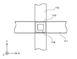
本実施の形態のもう一つの例に係る機械学習デバイスの記憶部11を実現する抵抗変化型メモリ11mは、図9にその構造を例示するように、下部電極ライン111と、上部電極ライン112との間にある抵抗変化層113内に、下部電極ライン111及び上部電極ライン112に対してそれぞれ平行に配された(従って互いに平行に配された状態にある)複数の抵抗保持層114a,b,…nを備える。なお、下部電極ライン111と上部電極ライン112とはそれぞれ複数本ずつ平行して互いに異なる面内(この面の法線方向をZ軸とする)に配され、下部電極ライン111と上部電極ライン112とのそれぞれの長手方向の角度は平面視では交差するように配される。具体的には下部電極ライン111の長手方向はX軸方向に配され、上部電極ライン112の長手方向はX軸方向に対して直交するY軸方向に配されるものとする(つまりここでもクロスバー構造を有する)。
本実施の形態の一例では、この抵抗保持層114は、抵抗変化層113内に析出する金属フィラメントの金属と同じ素材の金属を用いて形成するものとする。この抵抗保持層114が本発明の疑似電極に相当する。またこの抵抗保持層114は平面視では、ひとつのメモリセルに含まれる抵抗変化層113に内包される程度の大きさを有するものとする(図10)。
このように抵抗保持層114を備えたメモリセルにおいて上部電極ライン112と下部電極ライン111との間に印加する電圧を制御すると、当該メモリセルが保持する値が次のように変化する。なお、以下の例において、下部電極ライン111に最も近い側にある抵抗保持層114aを、第1の抵抗保持層114aと呼び、以下下部電極ライン111に近い順に、各抵抗保持層114b,c…nを、第2の抵抗保持層114b,第3の抵抗保持層114c…と呼ぶ。
このメモリセルにおいて当初、金属フィラメントが抵抗変化層113の下部電極ライン111側の端(以下、下端と呼ぶ)から第kの抵抗保持層114kまで成長した状態にあるとするとき、上部電極ライン112と下部電極ライン111との間に印加する電圧が所定の電位差Vthを下回るよう制御すると、図4(a)に示した例と同様、コンダクタンスは時間経過とともに成長に比べると迅速に減衰して、所定の時間(時間Tr)が経過した後、下端から金属フィラメントが第(k-1)番目の抵抗保持層114(k-1)まで成長した状態となる。この状態でさらに上部電極ライン112と下部電極ライン111との間に印加する電圧が所定の電位差Vthを下回るよう制御すると、コンダクタンスは時間経過とともにさらに減衰して、さらに所定の時間(時間Tr)が経過した後には、下端から金属フィラメントが第(k-2)番目の抵抗保持層114(k-2)まで成長した状態となる。以下、上記印加する電圧が所定の電位差Vthを下回るよう制御している間、次々とコンダクタンスが減少していく。このような印加電圧の制御を以下では「減衰制御」と呼ぶ。
また、このメモリセルにおいて、上部電極ライン112と下部電極ライン111との間に印加する電圧がこの所定の電位Vthから所定の範囲(Vthを超え、Vth+Vth′までの範囲とする)となるよう制御すると、金属フィラメントは成長も減衰もせず、その時点で金属フィラメントが抵抗変化層113の下部電極ライン111側の端(以下、下端と呼ぶ)から第kの抵抗保持層114kまで成長した状態にあったときには、その状態が維持される。この印加電圧の制御を、以下では「維持制御」と呼ぶ
なお、抵抗変化層の材質によっては、金属フィラメントがいずれかの抵抗保持層114まで成長した状態にあるときには、上部電極ライン112と下部電極ライン111との間の電位差がVthを下回るよう制御されても、下端からその時点で金属フィラメントが接触している抵抗保持層114(直近の下部電極ライン111に近い側の抵抗保持層)まで成長した状態が維持される。つまり、抵抗保持層114により、金属フィラメントの減衰が規制される。この場合に、記憶している値を「0」に近接させる際には、減衰制御を行う前に、印加電圧を、一時的にリセット電圧(例えば-(V0+ΔV))とするよう制御してもよい。なお、学習処理を行っている間は、リセット電圧の印加を行わないこととしてもよい。
また金属フィラメントが抵抗変化層113の下部電極ライン111側の端(以下、下端と呼ぶ)から第kの抵抗保持層114kまで成長した状態にあるときに、上部電極ライン112と下部電極ライン111との間に印加する電圧Vが所定の電位差Vthを超えて、V0+ΔV以上となる(V0+ΔV>Vth′)よう制御すると、図4(b)に例示したように、コンダクタンスは時間経過とともに指数関数的に増大して、所定の時間(時間Ts)が経過した後、金属フィラメントが、下端から次の(上部電極ライン112に近い側の)第(k+1)番目の抵抗保持層114(k+1)まで成長した状態となる。
この状態でさらに上部電極ライン112と下部電極ライン111との間に印加する電圧がV0+ΔV以上となるよう制御し続けると、コンダクタンスは時間経過とともにさらに指数関数的に増大して、また所定の時間(時間Ts)が経過した後には、下端から金属フィラメントが第(k+2)番目の抵抗保持層114(k+2)まで成長した状態となる。以下、上記印加する電圧がV0+ΔV以上であるよう制御されている間、次々とコンダクタンスが増大していく。この印加電圧の制御を、以下では「成長制御」と呼ぶ。
そしてこの例では、金属フィラメントが下端からどの抵抗保持層114a,b,…n(あるいは抵抗変化層113の上部電極ライン112側端部、以下「上端」という)まで成長しているかに対応する状態Gk(k=1,2,…)により、抵抗変化層113のコンダクタンスが、複数の状態Gkに対応する複数段階の保持値(コンダクタンス)のいずれかとなり、この段階のいずれかであれば、電圧を印加しない状態でも保持値であるコンダクタンスは維持される。
つまり、この抵抗変化層113を含むメモリセルは、電圧を印加しない状態で、単体で多値の情報を保持可能となる。なお、ここでの例でも最大のコンダクタンスの値を表す保持値を「1」、最小のコンダクタンスの値を表す保持値を「0」と規格化したものとして説明する。
このような多値の情報を保持可能な抵抗変化型メモリ11mを用いる場合、学習処理部13は次のように動作する。
この例における学習処理部13は、学習用に用意された複数の入力データを逐次的に情報入力部12から受け入れて、それぞれの入力データを、記憶部11に格納したニューラルネットワークに入力したときの、当該ニューラルネットワークの出力データを演算する。
この例においても入力データ及び出力データはいずれも、各データ要素が「0」または「1」となるバイナリ(2値)であるものとする(各ノードの値Ij,Ojが、Ij,Oj∈{0,1}である)とする。このとき学習処理部13は、隠れ層の各ノードHiの値を、
Hi=f(Σj Wi,j・Ij+b)
として演算する。ここでΣjは、jについて総和することを意味し、bは予め定められたバイアス値(スカラー値)である。また、関数f(X)は、既に述べた通り、X>0のとき「1」となり、そうでない場合は「0」となる二値化の関数である。
Hi=f(Σj Wi,j・Ij+b)
として演算する。ここでΣjは、jについて総和することを意味し、bは予め定められたバイアス値(スカラー値)である。また、関数f(X)は、既に述べた通り、X>0のとき「1」となり、そうでない場合は「0」となる二値化の関数である。
またこの例においても、一つの結合重みの情報Wi,jあたり一対のメモリセルを用い、各メモリセルがそれぞれ正の結合重みWi,j,+または負の結合重みWi,j,-の値を保持するものとする。そして結合重みの情報Wi,jは、これら2つの値の差Wi,j=(Wi,j,+)-(Wi,j,-)として表すものとする。本実施の形態のここでの例では、抵抗変化型メモリの各メモリセルにおいて多値の情報(0,G,2G,…nGのいずれかの値、ここでnは正の整数)が保持されているため、-nGから+nGまでの間の多値の表現が可能となる(ただし-1≦-nG<0<nG≦1)。
学習処理部13は、さらに、出力層の各ノードOjの値を、
Oj=f(Σi Wj,i・Hi+b)
として演算する。ここでΣiは、iについて総和することを意味する。その他の部分は隠れ層のノードの演算に用いたものと同様である(バイアスの値は隠れ層を演算する際の値と同じであっても、異なっていてもよい)。
Oj=f(Σi Wj,i・Hi+b)
として演算する。ここでΣiは、iについて総和することを意味する。その他の部分は隠れ層のノードの演算に用いたものと同様である(バイアスの値は隠れ層を演算する際の値と同じであっても、異なっていてもよい)。
次に学習処理部13は、出力データのうち、目的の値に達していないデータ要素の演算に係る結合重みの情報を保持する抵抗変化型メモリ11mのメモリセルに対して、目的の値に近接させる電気的信号を印加するよう制御する。ここでニューラルネットワークがオートエンコーダであるとすると、出力データの各データ要素の目的の値は、入力データの対応するデータ要素の値となる。
この学習処理部13は、出力データのj番目のデータ要素の値(ノードOjの値)が、入力データにおいて対応するj番目のデータ要素の値(ノードIjの値)と等しくないとき(Oj≠Ijのとき)に、隠れ層の各ノードHi(i=1,2,…)を順次参照し、隠れ層のi番目のノードの値が「1」(Hi=1)であるときに、次の動作を行う。
学習処理部13は、Oj≠Ijであるとき、Hi=1であるならば、さらに、Ij=0であるか否かを調べ、Ij=0であれば、Wi,j,+の値を保持する抵抗変化型メモリ11mのメモリセルに印加する電圧を、予め定めた時間ΔTp(以下、ΔT>Ts、かつΔT>Trとする)だけ、定常的に印加されている電圧V0からΔVだけ上昇させ、当該メモリセルにV0+ΔVの電位の電圧を印加するよう制御する(成長制御)。このとき学習処理部13は、Wi,j,-の値を保持する抵抗変化型メモリ11mのメモリセルに印加する電圧を、予め定めた時間ΔTmだけ、Vthを下回るよう制御する(減衰制御)。ここでΔTp,ΔTmは、既に説明した例と同様に定められる(以下同様)。
また学習処理部13は、Oj≠Ijであるとき、Hi=1であり、さらに、Ij=1であるならば、Wi,j,-の値を保持する抵抗変化型メモリ11mのメモリセルに印加する電圧を、予め定めた時間ΔTpだけ、定常的に印加されている電圧V0からΔVだけ上昇させ、当該メモリセルにV0+ΔVの電位の電圧を印加するよう制御する(成長制御)。このとき学習処理部13は、Wi,j,+の値を保持する抵抗変化型メモリ11mのメモリセルに印加する電圧を、ΔTmの時間だけ、Vthを下回るよう制御する(減衰制御)。
さらに学習処理部13は、Oj=Ijであるか、またはHi=0であるならば各メモリセルに印加する電圧を変化させないよう制御する(Wi,j,+、及びWi,j,-の値を保持する抵抗変化型メモリ11mのメモリセルに印加する電圧をV0に維持する:維持制御)。
またここでの例でも、学習処理部13が入力層、出力層の各ノードの値と、隠れ層の各ノードの値とを参照する代わりに、より簡便に、隠れ層のノードの値を参照することなく、入力層と出力層の各ノードの値のみを参照して学習処理を行ってもよい。
多値の結合重みの情報を保持するメモリセルを用いた場合の、この例に係る学習処理部13は、それぞれの入力データを、記憶部11に格納したニューラルネットワークに入力したときの、当該ニューラルネットワークの出力データを演算する処理までは上述と同様に動作する。
そして学習処理部13は、出力データのj番目のデータ要素の値(ノードOjの値)が、入力データにおいて対応するj番目のデータ要素の値(ノードIjの値)と等しくないとき(Oj≠Ijのとき)に、入力層の各ノードIi(i=1,2,…N、ただしi≠j)を順次参照し、隠れ層のi番目(iはjとは異なる)のノードの値が「1」(Ii=1)であるときに、次の動作を行う。
学習処理部13は、Oj≠Ijであるとき、Ii=1(j≠i)であるならば、さらに、Oj=0であるか否かを調べる。ここでOj=0であれば、Wi,j,+の値を保持する抵抗変化型メモリ11mのメモリセルに印加する電圧を、予め定めた時間ΔTpだけ、定常的に印加されている電圧V0からΔVだけ上昇させ、当該メモリセルにV0+ΔVの電位の電圧を印加するよう制御する(成長制御)。このとき、Wi,j,-の値を保持する抵抗変化型メモリ11mのメモリセルに印加する電圧は、予め定めた時間ΔTmに亘り、Vthを下回るよう制御する(減衰制御)。
また、学習処理部13は、Oj≠Ijであるとき、Oi=1(j≠i)であり、さらに、Oj=1であるならば、Wi,j,-の値を保持する抵抗変化型メモリ11mのメモリセルに印加する電圧を、予め定めた時間ΔTpだけ、定常的に印加されている電圧V0からΔVだけ上昇させ、当該メモリセルにV0+ΔVの電位の電圧を印加するよう制御する(成長制御)。このとき、Wi,j,+の値を保持する抵抗変化型メモリ11mのメモリセルに印加する電圧は、ΔTmの時間だけVthを下回るよう制御する(減衰制御)。
さらに学習処理部13は、Oj=Ijであるか、またはIi=0であるならば各メモリセルに印加する電圧を変化させないよう制御する(Wi,j,+、及びWi,j,-の値を保持する抵抗変化型メモリ11mのメモリセルに印加する電圧をV0に維持する:維持制御)。
これらの例の学習の処理においても、各ノードの値の比較は、いずれもAND回路等を用いて行うことができ、条件分岐はAND回路またはOR回路で実現でき、さらに電圧制御は、一般的な電圧制御回路によって実現できる。つまり、この学習処理部13は、必ずしもプログラム実行モジュールであるプロセッサ等を必要としない、比較的簡便な回路によって実現できる。また、プログラム実行モジュールを用いる場合も、比較的簡単な、比較及び条件分岐によって処理が実現できるため、そのプログラムも簡便で処理負荷の低いものとなっている。このように本実施の形態によれば、小規模なハードウェアによる学習を可能とし、ニューラルネットワークの利用場面を拡大できる。
[繰り返し学習]
さらに、このように多値の情報を保持可能な抵抗変化型メモリ11mを用いる場合も、維持制御の際の電位V0をVthから所定の電位Vmだけ下回る値に設定して、時間的にフィラメントを減衰させて用いてもよい。このようにすると、学習内容が時間経過とともに減衰して、自然な忘却処理が実現できる。
さらに、このように多値の情報を保持可能な抵抗変化型メモリ11mを用いる場合も、維持制御の際の電位V0をVthから所定の電位Vmだけ下回る値に設定して、時間的にフィラメントを減衰させて用いてもよい。このようにすると、学習内容が時間経過とともに減衰して、自然な忘却処理が実現できる。
さらに、このように金属フィラメントの減衰による忘却処理を用いる場合も、図6(b)に例示したように、学習処理部13が一つのデータセットを用いた学習処理を複数回繰り返して行ってもよい。
また、この場合の機械学習処理(図6の処理S2,図7の処理)でも、各メモリセルが保持する値の更新(メモリセルに印加する電圧の制御)を行う時間の間隔が、メモリセルに対して定常的に印加する電圧V0を印加したときに当該メモリセルのコンダクタンスが最大の状態から最小の状態まで減衰するのに要する時間Trより短い時間となるように上記電位Vmを設定するか、学習の処理を行うようにしてもよい。
[収束を学習の終了条件とする場合]
ここまでの説明において、同じデータセットを用いて繰り返して機械学習を行うときに、当該繰り返しを終了する条件は、繰り返し回数によって定めるものとしていたが、本実施の形態はこれに限られない。
ここまでの説明において、同じデータセットを用いて繰り返して機械学習を行うときに、当該繰り返しを終了する条件は、繰り返し回数によって定めるものとしていたが、本実施の形態はこれに限られない。
例えば機械学習処理(図6の処理S2,図7の処理)を行う際に、値を変更したメモリセルの数をカウントし、このカウント値が予め定めた閾値を下回ったときに、学習の内容が収束したものとして、機械学習処理の繰り返しを終了してもよい。
[チップ化]
また本実施の形態の機械学習デバイスは、記憶部11と、情報入力部12と、学習処理部13と、出力部14とを一つのチップとしてパッケージしたものとしてもよい。学習処理部13が既に述べたように、論理回路等、比較的簡易な回路で構成されるため、これらを一つのチップとしてパッケージしても回路が大規模化することがない。
また本実施の形態の機械学習デバイスは、記憶部11と、情報入力部12と、学習処理部13と、出力部14とを一つのチップとしてパッケージしたものとしてもよい。学習処理部13が既に述べたように、論理回路等、比較的簡易な回路で構成されるため、これらを一つのチップとしてパッケージしても回路が大規模化することがない。
[推論動作]
次に、以上のように機械学習を行った機械学習デバイスを用いて推論処理(例えば画像データの想起処理)を行う方法について説明する。この例では、推論のもととなる入力データを受け入れた機械学習デバイスの情報入力部12が、当該入力データに基づいて、記憶部11が結合重みの情報を保持するニューラルネットワークへ入力するためのベクトルデータを生成する。
次に、以上のように機械学習を行った機械学習デバイスを用いて推論処理(例えば画像データの想起処理)を行う方法について説明する。この例では、推論のもととなる入力データを受け入れた機械学習デバイスの情報入力部12が、当該入力データに基づいて、記憶部11が結合重みの情報を保持するニューラルネットワークへ入力するためのベクトルデータを生成する。
そして出力部14が記憶部11に保持されている結合重みWi,j,+及びWi,j,-とを用い、結合重みの情報Wi,j=(Wi,j,+)-(Wi,j,-)を得る。出力部14は、情報入力部12が生成したベクトルデータIj(j=1,2,…N)を用い、
隠れ層の各ノードHiの値を、
Hi=f(Σj Wi,j・Ij+b)
として演算する。そして出力部14はさらに、出力層の各ノードOjの値を、
Oj=f(Σi Wj,i・Hi+b)
として演算する。ここでWj,iは、入力層のj番目のノードIjと隠れ層のi番目のノードHiとの間の結合重みWをW=[Wi,j]と行列で表現したときの、隠れ層のi番目のノードHiと、出力層のj番目のノードOjとの間の結合重みである行列Wの転置行列WTのj行i列目の要素である。
隠れ層の各ノードHiの値を、
Hi=f(Σj Wi,j・Ij+b)
として演算する。そして出力部14はさらに、出力層の各ノードOjの値を、
Oj=f(Σi Wj,i・Hi+b)
として演算する。ここでWj,iは、入力層のj番目のノードIjと隠れ層のi番目のノードHiとの間の結合重みWをW=[Wi,j]と行列で表現したときの、隠れ層のi番目のノードHiと、出力層のj番目のノードOjとの間の結合重みである行列Wの転置行列WTのj行i列目の要素である。
すなわち、出力部14は、学習処理部13が出力層の各ノードの値を生成するのと同じ方法で推論処理を行う。そして出力部14は、当該出力層の各ノードの値を配列したベクトルデータを推論の結果として出力する。
Claims (10)
- 入力層と隠れ層と出力層とを含むニューラルネットワークの層間の結合重みの情報を抵抗変化型メモリ素子により保持する機械学習デバイスであって、
複数のデータ要素を含む入力データを受け入れ、前記ニューラルネットワークの前記結合重みの情報を用いて、複数のデータ要素を含む出力データを演算する演算手段と、
学習中は、前記出力データのうち、目的の値に達していないデータ要素の演算に係る前記結合重みの情報を保持する抵抗変化型メモリ素子に対し、目的の値に近接させる電気的信号を印加する学習処理を実行する学習手段と、
を含む機械学習デバイス。 - 請求項1記載の機械学習デバイスであって、
前記学習手段は、前記学習処理では、前記出力データのi番目(iは自然数)のデータ要素の値の目的の値を、前記入力データの、対応するi番目のデータ要素の値として、前記出力データのうち、当該目的の値に達していないデータ要素の演算に係る前記結合重みの情報を保持する抵抗変化型メモリ素子に対し、前記目的の値に近接させる電気的信号を印加する機械学習デバイス。 - 請求項1または2に記載の機械学習デバイスであって、
前記学習手段は、前記学習処理では、前記出力データのi番目のデータ要素の値の目的の値を、前記入力データの、対応するi番目のデータ要素の値として、
前記入力データのj番目(jは、i≠jなる自然数)の値が予め定めた条件を満足する値となっているときに、前記出力データのうち、当該目的の値に達していないデータ要素の演算に係る前記結合重みの情報を保持する抵抗変化型メモリ素子に対し、前記目的の値に近接させる電気的信号を印加する機械学習デバイス。 - 請求項1または2に記載の機械学習デバイスであって、
前記学習手段は、前記学習処理では、前記出力データのi番目のデータ要素の値の目的の値を、前記入力データの、対応するi番目のデータ要素の値として、
前記隠れ層のj(jは自然数)番目の要素が予め定めた値となっているときに、前記出力データのうち、当該目的の値に達していないデータ要素の演算に係り、前記j番目の隠れ層に関わる前記結合重みの情報を保持する抵抗変化型メモリ素子に対し、前記目的の値に近接させる電気的信号を印加する機械学習デバイス。 - 請求項1から4のいずれか一項に記載の機械学習デバイスであって、
前記入力層と隠れ層と出力層とにおける各データ要素の値はバイナリ値である機械学習デバイス。 - 請求項1から4のいずれか一項に記載の機械学習デバイスであって、
前記入力層と隠れ層と出力層とにおける各データ要素の値は離散的に定められたいずれかの値である機械学習デバイス。 - 請求項1から6のいずれか一項に記載の機械学習デバイスであって、
前記抵抗変化型メモリ素子の結合重みのそれぞれを保持する各セルは、定常状態では互いにコンダクタンスの異なる、Gk(k=0,1,…)の複数の状態のいずれかをとり、状態を変化させる電気的信号が印加されている間、変化状態となって、前記定常状態にて取り得る状態の間で変化し、当該所定の電気的信号の印加が終了した時点から前記定常状態のいずれかの状態に時間減衰して遷移する抵抗変化型メモリ素子であり、
前記学習手段は、複数の入力データを入力データセットとして受け入れて、当該入力データセットに含まれる入力データを順次用いて前記学習処理を実行し、当該学習処理の間に前記学習手段が目的の値に近接させる電気的信号を印加するときには、当該電気的信号の印加を予め定めた時間だけ続けて印加し、
前記学習手段は、一つの入力データセットに含まれる入力データを用いた学習処理を、予め定めた回数だけ繰り返し行う機械学習デバイス。 - 請求項7記載の機械学習デバイスであって、
前記抵抗変化型メモリ素子のセルの各々は、互いに実質的に平行に配された上部電極と下部電極との間に、抵抗変化層を配してなり、前記抵抗変化層内には、フィラメントの減衰を規制する平板状の疑似電極が少なくとも一つ、前記上部電極または下部電極に実質的に平行に配されてなる機械学習デバイス。 - 請求項8に記載の機械学習デバイスであって、
前記抵抗変化型メモリ素子のセルは二次元的な仮想的なXY平面に配列され、各セルの前記上部電極は前記XY平面を張るX軸またはY軸のいずれか一方の方向に隣接するセルの上部電極に互いに接続されてなり、
前記セルの前記下部電極は、前記XY平面を張るX軸またはY軸のいずれか他方の方向に隣接するセルの下部電極に互いに接続されてなる機械学習デバイス。 - 入力層と隠れ層と出力層とを含むニューラルネットワークの層間の結合重みの情報を抵抗変化型メモリ素子により保持する機械学習デバイスの制御方法であって、
演算手段が、複数のデータ要素を含む入力データを受け入れ、前記ニューラルネットワークの前記結合重みの情報を用いて、複数のデータ要素を含む出力データを演算する工程と、
学習手段が、学習中は、前記出力データのうち、目的の値に達していないデータ要素の演算に係る前記結合重みの情報を保持する抵抗変化型メモリ素子に対し、目的の値に近接させる電気的信号を印加する学習処理を実行する工程と、
を含む機械学習デバイスの制御方法。
Priority Applications (1)
| Application Number | Priority Date | Filing Date | Title |
|---|---|---|---|
| JP2020563869A JP7526484B2 (ja) | 2019-01-04 | 2019-12-25 | 機械学習デバイス、及びその制御方法 |
Applications Claiming Priority (2)
| Application Number | Priority Date | Filing Date | Title |
|---|---|---|---|
| JP2019-000307 | 2019-01-04 | ||
| JP2019000307 | 2019-01-04 |
Publications (1)
| Publication Number | Publication Date |
|---|---|
| WO2020141597A1 true WO2020141597A1 (ja) | 2020-07-09 |
Family
ID=71406865
Family Applications (1)
| Application Number | Title | Priority Date | Filing Date |
|---|---|---|---|
| PCT/JP2019/050971 Ceased WO2020141597A1 (ja) | 2019-01-04 | 2019-12-25 | 機械学習デバイス、及びその制御方法 |
Country Status (2)
| Country | Link |
|---|---|
| JP (1) | JP7526484B2 (ja) |
| WO (1) | WO2020141597A1 (ja) |
Citations (4)
| Publication number | Priority date | Publication date | Assignee | Title |
|---|---|---|---|---|
| JP2003163332A (ja) * | 2001-06-22 | 2003-06-06 | Matsushita Electric Ind Co Ltd | 半導体装置 |
| WO2018081600A1 (en) * | 2016-10-27 | 2018-05-03 | University Of Florida Research Foundation, Inc. | Learning algorithms for oscillatory memristive neuromorphic circuits |
| JP2018166194A (ja) * | 2017-03-28 | 2018-10-25 | 学校法人慶應義塾 | クロスバー構造および最適化問題解探索システム |
| WO2018235449A1 (ja) * | 2017-06-19 | 2018-12-27 | 株式会社デンソー | 人工ニューラルネットワーク回路の訓練方法、訓練プログラム、及び訓練装置 |
Family Cites Families (1)
| Publication number | Priority date | Publication date | Assignee | Title |
|---|---|---|---|---|
| US10332004B2 (en) * | 2015-07-13 | 2019-06-25 | Denso Corporation | Memristive neuromorphic circuit and method for training the memristive neuromorphic circuit |
-
2019
- 2019-12-25 WO PCT/JP2019/050971 patent/WO2020141597A1/ja not_active Ceased
- 2019-12-25 JP JP2020563869A patent/JP7526484B2/ja active Active
Patent Citations (4)
| Publication number | Priority date | Publication date | Assignee | Title |
|---|---|---|---|---|
| JP2003163332A (ja) * | 2001-06-22 | 2003-06-06 | Matsushita Electric Ind Co Ltd | 半導体装置 |
| WO2018081600A1 (en) * | 2016-10-27 | 2018-05-03 | University Of Florida Research Foundation, Inc. | Learning algorithms for oscillatory memristive neuromorphic circuits |
| JP2018166194A (ja) * | 2017-03-28 | 2018-10-25 | 学校法人慶應義塾 | クロスバー構造および最適化問題解探索システム |
| WO2018235449A1 (ja) * | 2017-06-19 | 2018-12-27 | 株式会社デンソー | 人工ニューラルネットワーク回路の訓練方法、訓練プログラム、及び訓練装置 |
Non-Patent Citations (2)
| Title |
|---|
| ISHIZAKA, MAMORU; SHINTANI, MICHIHIRO; INOUE, MICHIKO: "An Approach for Reliability Improvement of Memristor-based Neural Network through Weight Prediction", IEICE TECHNICAL REPORT, vol. 118, no. 334(VLD2018-50), 28 November 2018 (2018-11-28), pages 83 - 88, XP009522327, ISSN: 0913-5685 * |
| OKADA, MASARU; SUGITO, YASUMASA; HIKITA, WATARU; ASAI, TETSUYA; KUWAHARA, YUJI; AKAI-KASAYA, MEGUMI: "Autoencoder system fabricated with PEDOT:PSS wire", JAPAN SOCIETY OF APPLIED PHYSICS; EXTENDED ABSTRACTS OF THE 65TH JSAP SPRING MEETING, 2018, 5 March 2018 (2018-03-05), pages 11-240, XP009522326, ISBN: 978-4-86348-661-4 * |
Also Published As
| Publication number | Publication date |
|---|---|
| JP7526484B2 (ja) | 2024-08-01 |
| JPWO2020141597A1 (ja) | 2021-11-18 |
Similar Documents
| Publication | Publication Date | Title |
|---|---|---|
| Schuman et al. | Opportunities for neuromorphic computing algorithms and applications | |
| Lagoudakis et al. | Algorithm Selection using Reinforcement Learning. | |
| Lawrence et al. | Lessons in neural network training: Overfitting may be harder than expected | |
| CN110428042B (zh) | 往复地缩放神经元的连接权重和输入值来挫败硬件限制 | |
| Davis | Sensitivity analysis in neural net solutions | |
| Scellier | A deep learning theory for neural networks grounded in physics | |
| Kim et al. | Zero-shifting technique for deep neural network training on resistive cross-point arrays | |
| Xin et al. | Exploration entropy for reinforcement learning | |
| EP3859613A1 (en) | Information processing system, combinatorial optimization method, and combinatorial optimization program | |
| Baccetti et al. | Ergodicity, lack thereof, and the performance of reservoir computing with memristive networks | |
| JP6974955B2 (ja) | クロスバー構造および最適化問題解探索システム | |
| CN109697511A (zh) | 数据推理方法、装置及计算机设备 | |
| Wong et al. | Theory of associative memory in randomly connected Boolean neural networks | |
| JP7526484B2 (ja) | 機械学習デバイス、及びその制御方法 | |
| Li | Global optimization techniques based on swarm-intelligent and gradient-free algorithms | |
| Imada et al. | Evolution of Hop eld Model of Associative Memory by the Breeder Genetic Algorithm | |
| Katz et al. | Reinforcement-based program induction in a neural virtual machine | |
| Bengio et al. | An EM approach to learning sequential behavior | |
| Randall et al. | An extended extremal optimisation model for parallel architectures | |
| US20250217434A1 (en) | Performance of energy-based models using a hybrid thermodynamic-classical computing system | |
| Wu et al. | Finding quantum many-body ground states with artificial neural network | |
| Reers et al. | A new pattern for quantum evolutionary algorithms | |
| Evilevitch et al. | Avoiding Catastrophic Forgetting in Continual Learning through Elastic Weight Consolidation | |
| CN116976471B (zh) | 网络流量预测方法和装置 | |
| Yüzgülen | Neural Architecture Search with Zero-Cost Proxies |
Legal Events
| Date | Code | Title | Description |
|---|---|---|---|
| 121 | Ep: the epo has been informed by wipo that ep was designated in this application |
Ref document number: 19907822 Country of ref document: EP Kind code of ref document: A1 |
|
| ENP | Entry into the national phase |
Ref document number: 2020563869 Country of ref document: JP Kind code of ref document: A |
|
| NENP | Non-entry into the national phase |
Ref country code: DE |
|
| 122 | Ep: pct application non-entry in european phase |
Ref document number: 19907822 Country of ref document: EP Kind code of ref document: A1 |