WO2020133275A1 - 调光玻璃的驱动控制电路与调光玻璃 - Google Patents
调光玻璃的驱动控制电路与调光玻璃 Download PDFInfo
- Publication number
- WO2020133275A1 WO2020133275A1 PCT/CN2018/125065 CN2018125065W WO2020133275A1 WO 2020133275 A1 WO2020133275 A1 WO 2020133275A1 CN 2018125065 W CN2018125065 W CN 2018125065W WO 2020133275 A1 WO2020133275 A1 WO 2020133275A1
- Authority
- WO
- WIPO (PCT)
- Prior art keywords
- electrically connected
- branch
- inverter
- circuit
- dimming glass
- Prior art date
- Legal status (The legal status is an assumption and is not a legal conclusion. Google has not performed a legal analysis and makes no representation as to the accuracy of the status listed.)
- Ceased
Links
Images
Classifications
-
- H—ELECTRICITY
- H02—GENERATION; CONVERSION OR DISTRIBUTION OF ELECTRIC POWER
- H02M—APPARATUS FOR CONVERSION BETWEEN AC AND AC, BETWEEN AC AND DC, OR BETWEEN DC AND DC, AND FOR USE WITH MAINS OR SIMILAR POWER SUPPLY SYSTEMS; CONVERSION OF DC OR AC INPUT POWER INTO SURGE OUTPUT POWER; CONTROL OR REGULATION THEREOF
- H02M7/00—Conversion of AC power input into DC power output; Conversion of DC power input into AC power output
- H02M7/42—Conversion of DC power input into AC power output without possibility of reversal
- H02M7/44—Conversion of DC power input into AC power output without possibility of reversal by static converters
- H02M7/48—Conversion of DC power input into AC power output without possibility of reversal by static converters using discharge tubes with control electrode or semiconductor devices with control electrode
Definitions
- the invention relates to the field of dimming glass, in particular to the technology of controlling dimming glass to show different transparency.
- dimmable glass is also known as electronically controlled glass, photoelectric glass, electrically controlled intelligent glass, electro-induced liquid crystal atomized glass, etc. It is generally composed of outer glass, glass composite film, liquid crystal film, glass composite film, external A total of five layers of glass materials are compounded by a special process to form a whole; dimming glass has a blocking effect on infrared (heat energy) and ultraviolet light, and has good sound insulation and explosion-proof effects; when the dimming glass is powered off, the incident light Scattered when passing through disordered liquid crystal molecules, the glass is frosted, that is, opaque; when energized, the liquid crystal molecules are rearranged in a certain order, and the incident light can completely pass through the liquid crystal molecules at a certain angle to form a transparent state; As a capacitive load with AC characteristics, dimming glass has a maximum control voltage not exceeding the AC voltage of 75V.
- the control method of the dimming glass is mainly to directly control whether the driving voltage is provided in the dimming glass by turning on and off the switching element, that is, when the switch is turned on, the driving voltage is supplied to the dimming glass to drive it to full Transparent state; when the switch is turned off, the driving voltage stops being supplied to the dimming glass, and the dimming glass is opaque.
- this type of driving method can not freely control the transparency of the dimming glass, which limits the experience of using the dimming glass.
- a drive control circuit capable of accurately and conveniently adjusting the transparency of the dimming glass.
- a dimming glass including the aforementioned drive control circuit is also provided.
- An embodiment of the present invention discloses a drive control circuit for dimming glass, including:
- the input circuit is used to receive the first AC power
- a first conversion unit electrically connected to the input circuit, for converting the first AC power supply into a first DC power supply
- a second conversion unit electrically connected to the first conversion unit, for converting the first DC power supply into a second AC power supply, and the second AC power supply is used to drive the dimming glass body;
- a control unit electrically connected to the first conversion unit and the second conversion unit, for controlling the first conversion unit to convert the first AC power source into a first DC power source according to the control signal, the second The conversion unit provides corresponding second AC power to drive the dimming glass body according to the first DC power, different control signals correspond to different first DC power and second AC power, and different second AC power correspond to The dimming glass body has different transparency.
- An embodiment of the present invention discloses a dimming glass, including the aforementioned dimming glass drive control circuit and dimming glass body, wherein the dimming glass body is used for the second AC provided by the driving control circuit
- the power supply exhibits corresponding transparency; the input unit is disposed on the surface of the dimming glass body.
- the DC drive voltage corresponding to the required transparency is obtained through the DC conversion of the first conversion unit and the AC inverter conversion of the second conversion unit, because the voltage conversion control of the DC transformer is simpler and more accurate, which makes the final The obtained voltage in the second AC power source is more accurate.
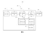
- 1 is a circuit block diagram of a dimming glass in an embodiment of the invention.
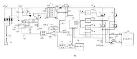
- FIG. 2 is a schematic diagram of the circuit structure of the drive control circuit shown in FIG. 1.
- the dimming glass 100 includes a driving control circuit 10 and a dimming glass body 20.
- the driving control circuit 10 is electrically connected to the dimming glass body 20, and is used to drive the dimming glass body 20 to present different transparency by providing driving voltages of different sizes to the dimming glass body 20.
- the drive control circuit 10 includes an input circuit 11, a filter rectifier circuit 12, a first conversion unit 13, a second conversion unit 14, a control unit 15, and an input unit 16.
- the input circuit 11 is configured to receive the first alternating current power supply AC1.
- the first AC power supply AC1 is 220V, 50HZ commercial power.
- the filtering and rectifying circuit 12 is electrically connected to the input circuit 11 and is used for performing a rectifying and filtering process on the first alternating current power supply AC1.
- the first conversion unit 13 is electrically connected to the input circuit 12 and is used to convert the rectified and filtered first AC power supply AC1 to the first DC power supply DC1.
- the voltage range of the first DC power supply is 0-90V.
- the second conversion unit 14 is electrically connected to the first conversion unit 13 for converting the first DC power supply DC1 into a second AC power supply AC2, wherein the second AC power supply AC2 is directly provided to the dimming glass
- the body 20 is used to drive the dimmable glass body 20 to have different transparency.
- the range of the voltage value of the second AC power source is 0-60V.
- the control unit 15 is electrically connected to the first conversion unit 13 and the second conversion unit 14, and is used to control the first conversion unit 13 to convert the first AC power source AC1 to the first DC power source DC1 according to the control signal.
- the second conversion unit 14 provides the corresponding second AC power AC2 to the dimming glass body 20 according to the first DC power DC1.
- different control signals correspond to different first DC power supplies DC1
- different first DC power supplies DC1 correspond to different second AC power supplies AC2
- different second AC power supplies AC2 correspond to different dimming glass bodies 20 Transparency, thereby causing the dimming glass body 20 to exhibit different transparency under different AC driving voltages in different second AC power sources AC2.
- the transparency of the dimming glass body 20 is proportional to the voltage value of the second AC power source.
- the input unit 16 is used to receive a user's touch operation and provide a corresponding control signal to the control unit 15 according to the touch operation, wherein different touch operations correspond to different control signals, that is, different touch operations
- the control signal is used to characterize the different transparency of the dimmable glass body 20.
- the different touch operations may be a combination of one or more factors in different operation positions, different operation times, different operation pressures, different operation durations, and different operation tracks. For example, the user inputs numbers representing different transparency through different touch operation traces, and the input unit 16 recognizes the touch operations to provide corresponding control signals to the control unit 15.
- the input unit 16 is disposed on the surface of the dimming glass body 20, and the input unit 16 is a flexible touch-sensitive panel.
- control unit 15 includes a microprocessor 151 and a digital potentiometer 153.
- the micro-processing unit 151 is electrically connected to the input unit 16 for receiving a control signal corresponding to the touch operation, and outputting a corresponding adjustment signal according to the control signal.
- the digital potentiometer 153 is electrically connected to the first conversion unit 13 and the micro-processing unit 151, and is used to adjust the output voltage according to the adjustment signal to the first conversion unit 13, and the first conversion unit 13 is based on The first direct current power supply DC1 corresponding to the adjusted voltage adjustment output.
- FIG. 2 is a schematic diagram of a specific circuit structure of the drive control circuit 10 shown in FIG. 1.
- the input circuit 11 may be a two-phase AC plug or a three-phase AC plug.
- one of the phases of the input circuit 11 is further provided with a fuse F1, which is used to cut off the flow of the first alternating current power supply AC1 to the drive control circuit 11 when an abnormal current flows.
- the filter rectifier circuit 12 is composed of a bridge rectifier circuit (not shown) composed of four rectifier diodes and a filter capacitor CE.
- the first conversion unit 13 includes an absorption circuit 131, a DC transformer 132, an output rectification filter circuit 133, a feedback sampling circuit 134, and a pulse width control circuit 135.
- the absorption circuit 131 is electrically connected between the filter rectifier circuit 12 and the DC transformer 132, and is used for absorbing surge and other abnormal current voltages for the filtered and rectified first AC power source AC1, including an absorption capacitor C1 and an absorption resistor R1 With absorption diode D1.
- the DC transformer 132 includes an AC input terminal 132A and a DC output terminal 132B, wherein the AC input terminal 132A is used to receive the first AC power source AC1, and the DC transformer 132 converts the first AC power source AC1 into a first DC power source DC1 Then, it is output from the DC output terminal 132B.
- the AC input terminal 132A includes a first winding input terminal W1 and a second winding input terminal W2, an absorption capacitor C1 and an absorption resistor R1 are connected in parallel between the first winding input terminal W1 and the second winding input terminal W2, and the absorption diode D1 is electrically connected Between the absorption resistor and the second winding input terminal W2.
- the DC transformer 132 further includes a first winding output terminal W3 and a second winding output terminal W4, the first winding output terminal W3 is electrically connected to the output filter rectifier circuit 133, and the second winding output terminal W4 is electrically connected to the protective ground terminal FGRD.
- the output rectifying and filtering circuit 133 is electrically connected to the first winding output end W3 of the DC transformer 132.
- the output rectification filter circuit 133 includes an output rectification diode DC1 and an output filter capacitor CC1.
- the output rectifier diode DC1 is electrically connected between the first winding output terminal W3 and the DC output terminal 132B, and the output filter capacitor CC1 is electrically connected between the DC output terminal 132B and the protective ground terminal FGND.
- the feedback sampling circuit 134 is used to detect the first DC power source DC1 and the adjustment voltage, and output a sampling adjustment signal to the pulse width control circuit 135 according to this.
- the feedback sampling circuit 134 includes a first sampling resistor RC1, a second sampling resistor RC2, a loop compensation circuit LC, a first operational amplifier circuit OP1, and a feedback photocoupler OCfb.
- the first sampling resistor RC1 and the second sampling resistor RC2 are connected in series between the DC output terminal 132B and the protective ground terminal FGND.
- the first operational amplifier circuit OP1 includes an in-phase input terminal N+, an inverting input terminal N-, and an operational output terminal O1, where the inverting input terminal N- is directly electrically connected between the first sampling resistor RC1 and the second sampling resistor RC2 Any one of the nodes, the non-inverting input terminal N+ is electrically connected to the digital potentiometer 153, and is used to receive the regulated voltage.
- the loop compensation circuit LC is electrically connected between the inverting input terminal N- and the operation output terminal O1.
- the operation output terminal O1 is electrically connected to the feedback optocoupler OCfb.
- the pulse width control circuit 135 is electrically connected to the DC transformer 132 and the feedback sampling circuit 134 for outputting a pulse width modulation signal to the DC transformer 132, and adjusting the pulse width modulation signal according to the sampling adjustment signal Duty cycle, the pulse width modulation signal is used to control the size of the first DC power supply DC1 converted and output by the DC transformer 132, and the pulse width modulation signals of different duty ratios correspond to different sizes of the first DC power supply DC1.
- the pulse width control circuit 135 includes a pulse width controller 1351, a first modulation resistor RP1, a second modulation resistor RP2, a modulation capacitor CR1, and a modulation transistor QR1.
- the pulse width controller 1351 is an integrated circuit including multiple pins.
- the feedback pin FB is electrically connected to the feedback optocoupler OCfb, and the power pin VDD is used to receive the driving power.
- the ground pin GND-P is electrically connected to the working ground GND, and the gate drive pin GATE is electrically connected to the gate of the modulation transistor Q1.
- the source of the modulation transistor Q1 is electrically connected to the input terminal W2 of the second winding, and the drain of the modulation transistor Q1 is electrically connected to the working ground GND through the second modulation resistor RP2. At the same time, it is also electrically connected to the modulation capacitor CR2 through the first modulation resistor RP1
- the working ground GND is connected to the ground, that is to say, the first modulation resistor RP1 and the modulation capacitor CR2 are connected in series between the drain of the modulation transistor Q1 and the working ground GND.
- the strobe pin CS is electrically connected to any node (not marked) between the first modulation resistor RP1 and the modulation capacitor CR2.
- the second conversion unit 14 includes an inverter controller 141, a full-bridge inverter circuit 143, a feedback resistor 145, an AC output filter circuit 147, an AC output terminal A+ and an AC output terminal A-.
- the AC output terminal A+ and the AC output terminal A- are electrically connected to the dimming glass body 20, and cooperate to output the second AC power source AC2.
- the AC output filter circuit 147 is electrically connected to the full-bridge inverter circuit 143 and the dimming glass body 20 for filtering the second AC power source AC2, including a first phase terminal 147a, a second phase terminal 147b, and an AC output Filter capacitor CO1 and AC output filter inductor LO1.
- the first phase terminal 147a is directly used as the AC output terminal A+, or the first phase terminal 147a is directly electrically connected to the AC output terminal A+, and the AC output filter capacitor CO1 is electrically connected to the first phase terminal 147a and the second phase terminal 147b In between, the AC output filter inductor LO1 is electrically connected between the second phase terminal 147b and the AC output terminal A-.
- the inverter controller 141 is an integrated circuit, including an enable pin EN, an inverter feedback pin IFB, a first gate control pin GATE1, a second gate control pin GATE2, a third gate control pin GATE3 and The fourth gate control pin GATE4.
- the enable pin EN is electrically connected to the micro-processing unit 151
- the inverter feedback pin IFB is electrically connected to the feedback resistor 145
- the four gate control pins GATE1 to GATE4 are electrically connected to the full-bridge inverter circuit 143 for The output gate control signal.
- the inverter controller 141 controls the corresponding four gate control pins GATE1 to GATE4 to output corresponding high and low potential switching signals when the enable pin EN receives the corresponding enable signal of the micro-processing unit 151, thereby starting the full-bridge inversion
- the transformer circuit 143 performs AC inverter conversion.
- the full-bridge inverter circuit 143 includes a first branch 143a, a second branch 143b, a third branch 143c, and a fourth branch 143d, wherein the first branch 143a and the third branch 143c are connected in series to the DC output Between the terminal and the protective ground terminal FGND, the second branch 143b and the fourth branch 143d are connected in series between the DC output terminal and the protective ground terminal FGND, and the first branch 143a and the third branch 143c The node between is electrically connected to the AC output terminal A-, and the node between the second branch 143b and the fourth branch 143d is electrically connected to the AC output terminal A+.
- the first branch 143a, the second branch 143b, the third branch 143c, and the fourth branch 143d are alternately turned on in two adjacent time periods in each cycle, thereby Form an AC power source. Specifically, in a cycle, during the first time period, the first branch 143a and the fourth branch 143 are turned on, and the second branch 143b and the third branch 143c are turned off, then the current direction is the direction of the first branch 143a The fourth branch 143d; in the second time period, the second branch 143b and the third branch 143d are on, the first branch 143a and the fourth branch 143d are off, then the current direction is the second branch 143b flowing to the first Three branches 143c.
- the first branch 143a includes a first inverter optocoupler OCi1 and a first inverter transistor Qi1.
- the first inverter optocoupler OCi1 is electrically connected between the first gate control pin GATE1 of the inverter controller 141 and the gate of the first inverter transistor Qi1, and the drain of the first inverter transistor Qi1 is electrically It is connected to the DC output terminal 132B, and the source of the first inverter transistor Qi1 is electrically connected to the second phase terminal 147b in the AC output filter circuit 147.
- the second branch 143b includes a second inverter optocoupler OCi2 and a second inverter transistor Qi2.
- the second inverter optocoupler OCi2 is electrically connected between the second gate control pin GATE2 of the inverter controller 141 and the gate of the second inverter transistor Qi2, and the drain of the second inverter transistor Qi2 is electrically It is connected to the DC output terminal 132B, and the source of the second inverter transistor Qi2 is electrically connected to the first phase terminal 147a in the AC output filter circuit 147.
- the third branch 143c includes a third inverter optocoupler OCi3 and a third inverter transistor Qi3.
- the third inverter optocoupler OCi3 is electrically connected between the third gate control pin GATE3 of the inverter controller 141 and the gate of the third inverter transistor Qi3, and the drain of the third inverter transistor Qi3 is electrically
- the second phase terminal 147b of the AC output filter circuit 147 is electrically connected, and the source of the third inverter transistor Qi3 is electrically connected to the protective ground terminal FGND through the feedback resistor 145.
- the fourth branch 143d includes a fourth inverter optocoupler OCi4 and a fourth inverter transistor Qi4.
- the fourth inverter optocoupler OCi4 is electrically connected between the fourth gate control pin GATE4 of the inverter controller 141 and the gate of the fourth inverter transistor Qi4, and the drain of the fourth inverter transistor Qi4 is electrically
- the first phase terminal 147a in the AC output filter circuit 147 is electrically connected, and the source of the fourth inverter transistor Qi4 is electrically connected to the protective ground terminal FGND through the feedback resistor 145.
- the inverter control circuit 141 controls the conduction time of the four branches in the full-bridge inverter circuit 143 through the four gate control pins to control the full-bridge inverter circuit 143 to invert the received first DC power source DC1 It is the second AC power source AC2, that is, the first DC power source DC is alternately circulated from two different phase directions to be converted into the second AC power source AC2.
- the inverter controller 141 obtains the voltage and current status of the second AC power supply AC2 through the voltage divided by the feedback resistor 145, and then adjusts the signals output by the four gate control pins to ensure the second AC power supply The voltage and current of AC2 are within the expected range.
- the filter rectifier circuit 12 After the input circuit 11 is connected to the AC power source, the first AC power source AC1 is transmitted to the filter rectifier circuit 12 through the input circuit 11, the filter rectifier circuit 12 performs rectifying and filtering processing on the first AC power source AC1, and absorbs the capacitance in the absorption circuit 131 C1, the absorption resistor R1 and the absorption diode D1 absorb the surge in the first AC power supply AC1, and ensure the normal input of the first AC power supply AC1.
- the DC transformer 132 performs DC conversion on the first AC power source AC1 and converts it into the first DC power source DC1.
- the first DC power source DC1 is output from the DC output terminal 132B after being subjected to the DC rectification and filtering process of the output rectification and filtering circuit 133.
- the input unit 16 receives the user's touch operation, for example, the user inputs a touch operation corresponding to 50% transparency, and the input unit 16 outputs a control signal corresponding to 50% transparency to the micro-processing unit 151, and the micro-processing unit 151 according to the processing signal
- the corresponding adjustment signal is output to the digital potentiometer 153.
- the digital potentiometer 153 adjusts its internal resistance according to the adjustment signal to output the adjustment voltage Vadj corresponding to the adjustment signal to the non-inverting input terminal N+ of the first operational amplifier circuit OP1 in the first conversion unit 13 .
- the voltage Vout of the first DC power source DC1 of the DC output terminal 132B is fed back to the inverting input terminal N- of the first operational amplifier circuit OP1 through the first sampling resistor RC1 and the second sampling resistor RC2.
- the voltage of the operational output terminal O1 of the first operational amplifier circuit OP1 controls the current and voltage of the feedback optocoupler OCfb according to the voltage applied to the non-inverting input terminal N+ and the inverting input terminal N-, and the pulse width control circuit 135 depends on the feedback optocoupler OCfb
- the second conversion unit 14 performs AC inversion according to the voltage Vout of the first DC power source DC1 adjusted according to the adjusted voltage Vadj.
- the first gate control pin GATE1 and the fourth gate control pin GATE4 of the inverter controller 141 output gate drive signals, and the first branch 143a and The fourth branch 143d is in a conducting state, and the first DC voltage Vout of the first DC power supply DC1 first passes through the first inverter transistor Qi1, the second phase terminal 147b, the AC output filter capacitor CO1, the first phase terminal 147a, the first Four inverter transistors Qi4, feedback resistor 145 and protective ground FGND.
- the second gate control pin GATE2 and the third gate control pin GATE3 of the inverter controller 141 output gate drive signals, and the second branch 143b and the third branch
- the path 143c is in an on state, and the first DC voltage Vout of the first DC power source DC1 passes through the second inverter transistor Qi2, the first phase terminal 147a, the AC output filter capacitor CO1, the second phase terminal 147b, and the third inverter transistor Qi3, feedback resistor 145 and protective ground FGND.
- the AC power obtained through the conduction directions of the four branches of the full-bridge inverter circuit 143 at different time points is output from the AC output terminal A+ and the AC output terminal A-, and passes through the AC output filter capacitor CO1 in the AC output filter circuit 147 And the AC output filter inductor LO1 is filtered and provided to the dimming glass body 20, thereby controlling the transparency of the dimming glass body 20 to correspond to the touch operation input.
- the voltage conversion control of the DC transformer 132 is simpler and more accurate. Therefore, the voltage in the second AC power supply AC2 finally obtained is more accurate.
- the DC transformer 132 in the first conversion unit 13 is now smaller in volume than the AC transformer, while the second conversion unit 14 directly uses a photocoupler and transistor to form a full-bridge inverter circuit 143.
- the AC inverter is also smaller, which makes the overall size of the drive control circuit 10 smaller, and the heat dissipation efficiency during operation increases, effectively improving the overall working stability of the control circuit 10.
Landscapes
- Engineering & Computer Science (AREA)
- Power Engineering (AREA)
- Inverter Devices (AREA)
Abstract
一种调光玻璃的驱动控制电路(10),包括输入电路(11)、第一转换单元(13)、第二转换单元(14)与控制单元(15)。输入电路(11)用于接收第一交流电源。第一转换单元(13)电连接输入电路(11)以用于将第一交流电源转换为第一直流电源。第二转换单元(14)电连接第一转换单元(13)以将第一直流电源转换为第二交流电源,第二交流电源用于驱动调光玻璃本体(20)。控制单元(15)电连接第一、二转换单元,用于依据控制信号控制第一转换单元(13)将第一交流电源转换为第一直流电源,第二转换单元(14)依据第一直流电源提供对应的第二交流电源驱动调光玻璃,不同的控制信号对应不同的第一直流电源与第二交流电源,不同的第二交流电源对应调光玻璃本体(20)不同的透明度。
Description
本发明涉及一种调光玻璃领域,具体涉及控制调光玻璃呈现不同透明度的技术。
调光玻璃作为建筑装饰特种玻璃又称为电控玻璃、光电玻璃、电控智能玻璃、电致液晶雾化玻璃等,一般是由外层玻璃、玻璃复合膜、液晶膜、玻璃复合膜、外层玻璃共五层材料经过特殊工艺复合而成形成一个整体;调光玻璃对红外线(热能)、紫外线具有阻隔作用,并具有良好的隔音、防爆效果;调光玻璃在断电情况下,入射光穿过无序排列的液晶分子时发生散射,玻璃外观呈磨砂状态,即不透明;当通电以后,液晶分子按一定顺序重新排列,入射光与液晶分子呈一定角度时可完全通过,形成透明状态;调光玻璃作为一种具有交流特性的容性负载,最高控制电压不超过交流电压AC 75V。
目前调光玻璃的控制方式主要是直接通过开关元件的接通和关断来控制调光玻璃中驱动电压是否提供,也即是当开关接通以后,驱动电压提供至调光玻璃驱动其为全透明状态;而当开关关断以后,驱动电压停止提供至调光玻璃,调光玻璃呈不透明状态。
明显可见,此类驱动方式完全不能自由控制调光玻璃的透明度,因而限制了调光玻璃的使用体验性。
发明内容
为解决前述问题,提供一种能够准确、方便地调整调光玻璃的透明度的驱动控制电路。
进一步,还提供一种包括前述驱动控制电路的调光玻璃。
本发明实施例公开了一种调光玻璃的驱动控制电路,包括:
输入电路,用于接收第一交流电源;
第一转换单元,电性连接所述输入电路,用于将所述第一交流电源转换为 第一直流电源;
第二转换单元,电性连接所第一转换单元,用于将所述第一直流电源转换为第二交流电源,所述第二交流电源用于驱动调光玻璃本体;
控制单元,电性连接所第一转换单元与所述第二转换单元,用于依据控制信号控制所述第一转换单元将所述第一交流电源转换为第一直流电源,所述第二转换单元依据所述第一直流电源提供相应的第二交流电源驱动所述调光玻璃本体,不同的控制信号对应不同的第一直流电源与第二交流电源,不同的第二交流电源对应所述调光玻璃本体不同的透明度。
本发明实施例公开了一种调光玻璃,包括前述调光玻璃的驱动控制电路与调光玻璃本体,其中,所述调光玻璃本体用于依据所述驱动控制电路提供的所述第二交流电源呈现对应的透明度;所述输入单元设置于所述调光玻璃本体表面。
相较于现有技术,经过第一转换单元的直流转换以及第二转换单元的交流逆变转换而获得对应需求透明度的交流驱动电压,由于直流变压器的电压转换控制更加简单与准确,从而使得最后获得的第二交流电源中的电压更加准确。
为了更清楚地说明本发明实施例中的技术方案,下面将对实施例中所需要使用的附图作简单地介绍,显而易见地,下面描述中的附图仅仅是本发明的一些实施例,对于本领域普通技术人员来讲,在不付出创造性劳动性的前提下,还可以根据这些附图获得其他的附图。
图1为本发明一实施例中调光玻璃的电路框图;
图2为如图1所示驱动控制电路的电路结构示意图。
下面将结合本发明实施例中的附图,对本发明实施例中的技术方案进行清楚、完整地描述,显然,所描述的实施例仅是本发明一部分实施例,而不是全部的实施例。基于本发明中的实施例,本领域普通技术人员在没有做出创造性劳动前提下所获得的所有其他实施例,都属于本发明保护的范围。
下面结合附图,具体说明调光玻璃的驱动电路及其工作原理。
如图1所示,其为本发明一实施例中调光玻璃的电路框图,调光玻璃100包括驱动控制电路10与调光玻璃本体20。
驱动控制电路10电性连接调光玻璃本体20,并且用于通过提供不同大小的驱动电压给调光玻璃本体20,从而驱动调光玻璃本体20呈现不同的透明度。
其中,驱动控制电路10包括输入电路11、滤波整流电路12、第一转换单元13、第二转换单元14、控制单元15以及输入单元16。
输入电路11,用于接收第一交流电源AC1。本实施例中,第一交流电源AC1为220V、50HZ的市电。
滤波整流电路12电性连接输入电路11,用于针对第一交流电源AC1执行整流滤波处理。
第一转换单元13电性连接输入电路12,用于将经过整流滤波处理的第一交流电源AC1转换为第一直流电源DC1。本实施例中,第一直流电源的电压值范围为0-90V。
第二转换单元14,电性连接所第一转换单元13,用于将所述第一直流电源DC1转换为第二交流电源AC2,其中,所述第二交流电源AC2直接提供给调光玻璃本体20,用于驱动调光玻璃本体20处于不同透明度。本实施例中,第二交流电源的电压值的范围为0-60V。
控制单元15,电性连接第一转换单元13与第二转换单元14,用于依据控制信号控制所述第一转换单元13将所述第一交流电源AC1转换为第一直流电源DC1,所述第二转换单元14依据所述第一直流电源DC1提供对应的第二交流电源AC2至调光玻璃本体20。其中,不同的控制信号对应不同的第一直流电源DC1,不同的第一直流电源DC1对应不同的第二交流电源AC2,不同的第二交流电源AC2对应所述调光玻璃本体20不同的透明度,由此使得所述调光玻璃本体20在不同的第二交流电源AC2中交流驱动电压下呈现不同的透明度。
较佳地,调光玻璃本体20的透明度与所述第二交流电源的电压值成正比。
输入单元16用于接收用户的触摸操作,并且依据所述触摸操作提供对应的控制信号至所述控制单元15,其中,不同的触摸操作对应不同的控制信号,也即是不同的所述触摸操作与所述控制信号用于表征调光玻璃本体20的不同 透明度。所述不同的触摸操作可以为不同的操作位置、不同的操作时间、不同的操作压力、不同的操作时长、不同的操作轨迹中其中一个或者多个的因素的组合。举例而言,用户通过不同的触摸操作轨迹而输入表征不同透明度的数字,输入单元16识别该些触摸操作从而提供对应不同的控制信号至所述控制单元15。
较佳地,当触摸操作为连续操作时,调光玻璃本体20的透明度为连续变化。本实施例中,输入单元16设置于调光玻璃本体20表面,并且输入单元16为柔性触摸感应面板。
更为具体的,所述控制单元15包括微处理器151与数字电位器153。其中,微处理单元151电性连接所述输入单元16,用于接收与对应所述触摸操作的控制信号,并且依据所述控制信号输出对应的调整信号。数字电位器153电性连接所述第一转换单元13与所述微处理单元151,用于依据所述调整信号输出的调整电压至所述第一转换单元13,第一转换单元13则依据所述调整电压调整输出对应的第一直流电源DC1。
请参阅图2,其为如图1所示驱动控制电路10的具体电路结构示意图。
如图2所示,输入电路11可以为二相交流插头或者三相交流插头。较佳地,输入电路11中的其中一相上还设置有保险丝F1,以用于对流过异常电流是切断第一交流电源AC1流入驱动控制电路11。
滤波整流电路12为由4个整流二极管组合而成的桥式整流电路(未标示)以及的滤波电容CE构成。
第一转换单元13包括吸收电路131、直流变压器132、输出整流滤波电路133、反馈采样电路134以及脉宽控制电路135。
具体地,吸收电路131电性连接滤波整流电路12与直流变压器132之间,用于针对滤波整流后的第一交流电源AC1进行浪涌等异常电流电压进行吸收,包括吸收电容C1、吸收电阻R1与吸收二极管D1。
直流变压器132包括交流输入端132A与直流输出端132B,其中,所述交流输入端132A用于接收所述第一交流电源AC1,直流变压器132将第一交流电源AC1转换为第一直流电源DC1后,自直流输出端132B输出。
交流输入端132A包括第一绕组输入端W1与第二绕组输入端W2,吸收电容C1与吸收电阻R1并联于第一绕组输入端W1与第二绕组输入端W2之间,吸收二极管D1电性连接于吸收电阻与第二绕组输入端W2之间。
直流变压器132还包括第一绕组输出端W3与第二绕组输出端W4,第一绕组输出端W3电性连接输出滤波整流电路133,第二绕组输出端W4电性连接保护接地端FGRD。
输出整流滤波电路133电性连接于直流变压器132的第一绕组输出端W3。输出整流滤波电路133包括输出整流二极管DC1与输出滤波电容CC1。其中,输出整流二极管DC1电性连接于第一绕组输出端W3与直流输出端132B之间,输出滤波电容CC1电性连接于直流输出端132B与保护接地端FGND之间。
反馈采样电路134用于检测第一直流电源DC1与调整电压,并且据此输出采样调整信号至脉宽控制电路135。
具体地,反馈采样电路134包括第一采样电阻RC1、第二采样电阻RC2、环路补偿电路LC、第一运算放大电路OP1以及反馈光耦OCfb。
其中,第一采样电阻RC1与第二采样电阻RC2串联于直流输出端132B与保护接地端FGND之间。
第一运算放大电路OP1包括同相输入端N+、反相输入端N-以及运算输出端O1,其中,反相输入端N-直接电性连接于第一采样电阻RC1与第二采样电阻RC2之间的任意一个节点,同相输入端N+电性连接于数字电位器153,用于接收调节电压。环路补偿电路LC电性连接于反相输入端N-与运算输出端O1之间。运算输出端O1电性连接于反馈光耦OCfb。
脉宽控制电路135电性连接所述直流变压器132与所述反馈采样电路134,用于输出脉宽调制信号至所述直流变压器132,并且依据所述采样调整信号调整所述脉宽调制信号的占空比,所述脉宽调制信号用于控制所述直流变压器132转换输出的所述第一直流电源DC1的大小,且不同占空比的所述脉宽调制信号对应不同大小的第一直流电源DC1。
所述脉宽控制电路135包括脉宽控制器1351、第一调制电阻RP1、第二调制电阻RP2、调制电容CR1以及调制晶体管QR1。
本实施例中,脉宽控制器1351为包括多个引脚的集成电路,其中,脉宽 控制器1351中,反馈引脚FB电性连接反馈光耦OCfb,电源引脚VDD用于接收驱动电源,接地引脚GND-P电性连接工作接地端GND,栅极驱动引脚GATE电性连接调制晶体管Q1的栅极。
调制晶体管Q1的源极电性连接第二绕组输入端W2,调制晶体管Q1的漏极通过第二调制电阻RP2电性连接工作接地端GND,同时,还通过第一调制电阻RP1与调制电容CR2电性连接工作接地端GND而接地,也即是说,第一调制电阻RP1与调制电容CR2串联于调制晶体管Q1的漏极与工作接地端GND之间。
较佳地,选通引脚CS电性连于第一调制电阻RP1与调制电容CR2之间任意一个节点(未标示)。
所述第二转换单元14包括逆变控制器141、全桥逆变电路143、反馈电阻145、交流输出滤波电路147、交流输出端A+与交流输出端A-。
其中,交流输出端A+与交流输出端A-电性连接于调光玻璃本体20,并且相互配合输出第二交流电源AC2。
交流输出滤波电路147电性连接所述全桥逆变电路143以及调光玻璃本体20,用于针对第二交流电源AC2进行滤波处理,包括第一相位端147a、第二相位端147b,交流输出滤波电容CO1以及交流输出滤波电感LO1。其中,第一相位端147a直接作为交流输出端A+,或者说第一相位端147a直接电性连接交流输出端A+,交流输出滤波电容CO1电性连接于第一相位端147a与第二相位端147b之间,交流输出滤波电感LO1电性连接于第二相位端147b与交流输出端A-之间。
逆变控制器141为集成电路,包括使能引脚EN、逆变反馈引脚IFB、第一栅极控制引脚GATE1、第二栅极控制引脚GATE2、第三栅极控制引脚GATE3以及第四栅极控制引脚GATE4。
其中,使能引脚EN电性连接微处理单元151,逆变反馈引脚IFB电性连接于反馈电阻145,四个栅极控制引脚GATE1~GATE4电性连接全桥逆变电路143,用于输出栅极控制信号。逆变控制器141在使能引脚EN接收到微处理单元151相应的使能信号时控制对应的四个栅极控制引脚GATE1~GATE4输出对应高、低电位开关信号,从而启动全桥逆变电路143执行交流逆变转换。
全桥逆变电路143包括第一支路143a、第二支路143b、第三支路143c、第 四支路143d,其中,第一支路143a与第三支路143c串联于所述直流输出端与所述保护接地端FGND之间,第二支路143b与第四支路143d串联于所述直流输出端与所述保护接地端FGND之间,第一支路143a与第三支路143c之间的节点电性连接于交流输出端A-,第二支路143b与第四支路143d之间的节点电性连接于交流输出端A+。
第一支路143a、第二支路143b、第三支路143c、第四支路143d在逆变控制器141控制下在每个周期中的2个相邻时间段两两交替导通,从而形成交流电源。具体的,在一个周期中,第一时间段,第一支路143a与第四支路143导通,第二支路143b与第三支路143c截止,则电流方向为第一支路143a流向第四支路143d;在第二时间段,第二支路143b与第三支路143d导通,第一支路143a与第四支路143d截止,则电流方向为第二支路143b流向第三支路143c。
具体地,第一支路143a包括第一逆变光耦OCi1与第一逆变晶体管Qi1。其中,第一逆变光耦OCi1电性连接于逆变控制器141的第一栅极控制引脚GATE1与第一逆变晶体管Qi1的栅极之间,第一逆变晶体管Qi1的漏极电性连接直流输出端132B,第一逆变晶体管Qi1的源极电性连接交流输出滤波电路147中的第二相位端147b。
第二支路143b包括第二逆变光耦OCi2与第二逆变晶体管Qi2。其中,第二逆变光耦OCi2电性连接于逆变控制器141的第二栅极控制引脚GATE2与第二逆变晶体管Qi2的栅极之间,第二逆变晶体管Qi2的漏极电性连接直流输出端132B,第二逆变晶体管Qi2的源极电性连接交流输出滤波电路147中的第一相位端147a。
第三支路143c包括第三逆变光耦OCi3与第三逆变晶体管Qi3。其中,第三逆变光耦OCi3电性连接于逆变控制器141的第三栅极控制引脚GATE3与第三逆变晶体管Qi3的栅极之间,第三逆变晶体管Qi3的漏极电性连接交流输出滤波电路147中的第二相位端147b,第三逆变晶体管Qi3的源极通过反馈电阻145电性连接保护接地端FGND。
第四支路143d包括第四逆变光耦OCi4与第四逆变晶体管Qi4。其中,第四逆变光耦OCi4电性连接于逆变控制器141的第四栅极控制引脚GATE4与第四逆变晶体管Qi4的栅极之间,第四逆变晶体管Qi4的漏极电性连接交流输出滤波 电路147中的第一相位端147a,第四逆变晶体管Qi4的源极通过反馈电阻145电性连接保护接地端FGND。
逆变控制电路141通过四个栅极控制引脚控制全桥逆变电路143中四个支路的导通时间,以控制全桥逆变电路143将接收的第一直流电源DC1逆变转换为第二交流电源AC2,也即是说将所述第一直流电源DC从两个不同相位方向交替流通而转换为第二交流电源AC2。
较佳地,逆变控制器141通过反馈电阻145分取的电压获知第二交流电源AC2的电压、电流状态,进而针对四个栅极控制引脚输出的信号进行调整,以保证第二交流电源AC2的电压、电流处于期望值范围内。
现在结合图2,具体说明驱动控制电路10对调光玻璃本体20的驱动过程。
当输入电路11接通到交流电源以后,第一交流电源AC1通过输入电路11传输至滤波整流电路12,滤波整流电路12针对第一交流电源AC1进行整流滤波处理,同时吸收电路131中的吸收电容C1、吸收电阻R1与吸收二极管D1针对第一交流电源AC1中的浪涌进行吸收,保证第一交流电源AC1的正常输入。
直流变压器132针对第一交流电源AC1进行直流转换,并且转换为第一直流电源DC1,第一直流电源DC1经过输出整流滤波电路133的直流整流滤波处理后自直流输出端132B输出。
与此同时,输入单元16接收用户的触摸操作,例如用户输入对应透明度50%的触摸操作,输入单元16则输出对应透明度50%的控制信号至微处理单元151,微处理单元151依据该处理信号输出对应的调整信号至数字电位器153,数字电位器153依据调整信号调整其内部电阻从而输出与调整信号对应的调整电压Vadj至第一转换单元13中第一运算放大电路OP1的同相输入端N+。
直流输出端132B的第一直流电源DC1的电压Vout通过第一采样电阻RC1与第二采样电阻RC2反馈至第一运算放大电路OP1的反相输入端N-。
第一运算放大电路OP1的运算输出端O1的电压则依据同相输入端N+与反相输入端N-加载的电压控制反馈光耦OCfb的电流、电压,脉宽控制电路135则依据反馈光耦OCfb的电流、电压输出对应占空比的脉宽调制信号至调制晶体管QR1的栅极,进而控制调制晶体管QR1的通断时间,由于调制晶体管QR1的 通断时间直接决定直流变压器132输入的交流电压的时间,进而针对直流变压器132输出的第一直流电源DC1的第一直流电压Vout与调整电压Vadj相近。
第二转换单元14依据对应调整电压Vadj调整后的第一直流电源DC1的电压Vout进行交流逆变。
具体地,对于第一相位,例如0-180°相位,逆变控制器141的第一栅极控制引脚GATE1与第四栅极控制引脚GATE4输出栅极驱动信号,第一支路143a与第四支路143d处于导通状态,第一直流电源DC1的第一直流电压Vout首先经由第一逆变晶体管Qi1、第二相位端147b、交流输出滤波电容CO1、第一相位端147a、第四逆变晶体管Qi4、反馈电阻145以及保护接地端FGND。
对于第二相位,例如180-360°相位,逆变控制器141的第二栅极控制引脚GATE2与第三栅极控制引脚GATE3输出栅极驱动信号,第二支路143b与第三支路143c处于导通状态,第一直流电源DC1的第一直流电压Vout经由第二逆变晶体管Qi2、第一相位端147a、交流输出滤波电容CO1、第二相位端147b、第三逆变晶体管Qi3、反馈电阻145以及保护接地端FGND。
经过全桥逆变电路143中四个支路的不同时间点的导通方向获得的交流电源自交流输出端A+与交流输出端A-输出,并且经过交流输出滤波电路147中交流输出滤波电容CO1以及交流输出滤波电感LO1滤波处理后提供到调光玻璃本体20中,从而控制调光玻璃本体20处于对应触摸操作输入的透明度。
相较于现有技术,经过第一转换单元13的直流转换以及第二转换单元14的交流逆变转换而获得对应需求透明度的交流驱动电压,由于直流变压器132的电压转换控制更加简单与准确,从而使得最后获得的第二交流电源AC2中的电压更加准确。与此同时,第一转换单元13中的直流变压器132现对于交流变压器体积较小,而第二转换单元14直接采用光耦与晶体管的方式构成全桥逆变电路143的体积相较于绕组形式的交流逆变器也更小,进而使得驱动控制电路10整体的体积较小,并且工作时散热效率增加,有效提高了控制电路10整体工作稳定性。
本文中应用了具体个例对本发明的原理及实施方式进行了阐述,以上实施例的说明只是用于帮助理解本发明的核心思想;同时,对于本领域的一般技术人员,依据本发明的思想,在具体实施方式及应用范围上均会有改变之处, 综上所述,本说明书内容不应理解为对本发明的限制。
Claims (15)
- 一种调光玻璃的驱动控制电路,其特征在于,包括:输入电路,用于接收第一交流电源;第一转换单元,电性连接所述输入电路,用于将所述第一交流电源转换为第一直流电源;第二转换单元,电性连接所第一转换单元,用于将所述第一直流电源转换为第二交流电源,所述第二交流电源用于驱动调光玻璃本体;控制单元,电性连接所第一转换单元与所述第二转换单元,用于依据控制信号控制所述第一转换单元将所述第一交流电源转换为第一直流电源,所述第二转换单元依据所述第一直流电源提供相应的第二交流电源驱动所述调光玻璃本体,不同的控制信号对应不同的第一直流电源与第二交流电源,不同的第二交流电源对应所述调光玻璃本体不同的透明度。
- 根据权利要求1所述的调光玻璃的驱动控制电路,其特征在于,所述调光玻璃本体的透明度与所述第二交流电源的电压值成正比。
- 根据权利要求2所述的调光玻璃的驱动控制电路,其特征在于,所述调光玻璃本体的透明度为连续变化。
- 根据权利要求2所述的调光玻璃的驱动控制电路,其特征在于,所述驱动控制电路还包括:输入单元,用于接收用户的触摸操作,并且依据所述触摸操作提供对应的控制信号至所述控制单元,所述控制单元根据控制信号调节调光玻璃本体的透明度,其中,不同的触摸操作对应不同的控制信号。
- 根据权利要求4所述的调光玻璃的驱动控制电路,其特征在于,所述控制单元包括:微处理单元,电性连接所述输入单元,用于接收与对应所述触摸操作的控制信号,并且依据所述控制信号输出对应的调整信号;数字电位器,电性连接所述第一转换单元与所述微处理单元,用于依据所述调整信号输出调整电压至所述第一转换单元,所述第一转换单元依据所述调整电压输出对应的第一直流电源。
- 根据权利要求5所述的调光玻璃的驱动控制电路,其特征在于,所述第一转换单元包括:直流变压器,包括交流输入端与直流输出端,所述交流输入端用于接收所述第一交流电源,所述直流变压器将所述第一交流电源转换为所述第一直流电源且自所述直流输出端输出;反馈采样电路,用于检测所述第一直流电源与所述调整电压,并且据此输出采样调整信号;脉宽驱动控制电路,电性连接所述直流变压器与所述反馈采样电路,用于输出脉宽调制信号至所述直流变压器,并且依据所述采样调整信号调整所述脉宽调制信号的占空比,所述脉宽调制信号用于控制所述直流变压器转换输出的所述第一直流电源的大小,且不同占空比的所述脉宽调制信号对应不同大小的第一直流电源。
- 根据权利要求6所述的调光玻璃的驱动控制电路,其特征在于,所述反馈采样电路包括第一采样电阻、第二采样电阻、环路补偿电路、第一运算放大电路以及反馈光耦,其中,所述第一采样电阻与所述第二采样电阻串联于所述直流输出端与保护接地端之间,所述第一运算放大电路包括同相输入端、反相输入端以及运算输出端,所述反相输入端电性连接于所述第一采样电阻与所述第二采样电阻之间的任意一个节点,所述同相输入端电性连接于所述数字电位器以用于接收所述调节电压,所述环路补偿电路电性连接于所述反相输入端与所述运算输出端之间,所述运算输出端电性连接于所述反馈光耦。
- 根据权利要求7所述的调光玻璃的驱动控制电路,其特征在于,所述脉宽驱动控制电路包括脉宽控制器、第一调制电阻、第二调制电阻、调制电容以及调制晶体管,脉宽控制器包括反馈引脚与栅极驱动引脚,其中,所述反馈引脚电性连接所述反馈光耦,所述栅极驱动引脚电性连接所述调制晶体管的栅极;所述调制晶体管的源极电性连接所述直流变压器的交流输入端,所述调制晶体管的漏极通过所述第二调制电阻电性连接工作接地端,并且通过所述第一调制电阻与所述调制电容电性连接工作接地端。
- 根据权利要求7所述的调光玻璃的驱动控制电路,其特征在于,所述交流输入端包括第一绕组输入端与第二绕组输入端;所述第一转换单元还包括吸收电路,所述吸收电路用于对经过所述第一交流电源的浪涌吸收,所述吸收电路包括吸收电容、吸收电阻与吸收二极管,其中,所述吸收电容与所述吸收电阻并联于所述第一绕组输入端与所述第二绕组输入端之间,所述吸收二极管电性连接于所述吸收电阻与所述第二绕组输入端之间。
- 根据权利要求1所述的调光玻璃的驱动控制电路,其特征在于,所述第二转换单元包括交流输出滤波电路、相互电性连接的逆变控制器与全桥逆变电路,所述全桥逆变电路接收所述第一直流电源,所述逆变控制电路控制所述全桥逆变电路接收的第一直流电源逆变转换为所述第二交流电源;所述交流输出滤波电路电性连接所述全桥逆变电路以及所述调光玻璃本体,用于对所述第二交流电源进行滤波处理,所述交流输出滤波电路包括第一相位端、第二相位端,交流输出滤波电容以及交流输出滤波电感,所述第一相位端作为所述用于输出第二交流电源其中一个交流输出端,所述交流输出滤波电容电性连接于第一相位端与所述第二相位端之间,所述交流输出滤波电感电性连接于第二相位端与所述用于输出第二交流电源的另外一个交流输出端之间。
- 根据权利要求10所述的调光玻璃的驱动控制电路,其特征在于,全桥逆变电路包括第一支路、第二支路、第三支路、第四支路,所述第一支路与所述第三支路串联于所述直流输出端与所述保护接地端之间,所述第二支路与所 述第四支路串联于所述直流输出端与所述保护接地端之间,所述第一支路与所述第三支路之间的节点、以及所述第二支路与所述第四支路之间的节点分别电性连接所述用于输出第二交流电源的两个交流输出端,其中,所述第一支路、所述第二支路、所述第三支路以及所述第四支路在所述逆变控制器控制下在每个周期中的两个相邻时间段两两交替导通以形成所述第二交流电源。
- 根据权利要求11所述的调光玻璃的驱动控制电路,其特征在于,在一个周期中的第一时间段,所述第一支路与所述第四支路导通,所述第二支路与所述第三支路截止,电流方向为所述自第一支路流向第四支路;在第二时间段,所述第二支路与所述第三支路导通,所述第一支路与所述第四支路截止,电流方向为自所述第二支路流向所述第三支路。
- 根据权利要求11所述的调光玻璃的驱动控制电路,其特征在于,所述第一支路包括第一逆变光耦与第一逆变晶体管,所述第一逆变光耦电性连接于所述逆变控制器的第一栅极控制引脚与所述第一逆变晶体管的栅极之间,所述第一逆变晶体管的漏极电性连接所述直流输出端,所述第一逆变晶体管的源极电性连接所述交流输出滤波电路中的第二相位端;所述第二支路包括第二逆变光耦与第二逆变晶体管,所述第二逆变光耦电性连接于所述逆变控制器的第二栅极控制引脚与所述第二逆变晶体管的栅极之间,所述第二逆变晶体管的漏极电性连接所述直流输出端,所述第二逆变晶体管的源极电性连接所述交流输出滤波电路中的第一相位端;所述第三支路包括第三逆变光耦与第三逆变晶体管,所述第三逆变光耦电性连接于所述逆变控制器的所述第三栅极控制引脚与所述第三逆变晶体管的栅极之间,所述第三逆变晶体管的漏极电性连接所述交流输出滤波电路中的第二相位端,所述第三逆变晶体管的源极通过反馈电阻电性连接所述保护接地端;所述第四支路包括第四逆变光耦与第四逆变晶体管,所述第四逆变光耦电性连接于所述逆变控制器的第四栅极控制引脚与所述第四逆变晶体管的栅极之间,所述第四逆变晶体管的漏极电性连接所述交流输出滤波电路的第一相位端,所述第四逆变晶体管的源极通过所述反馈电阻电性连接所述保护接地端。
- 一种调光玻璃,其特征在于,包括如权利要求1-13任意一项所述的调光玻璃的驱动控制电路与调光玻璃本体,其中,所述调光玻璃本体用于依据所述驱动控制电路提供的所述第二交流电源呈现对应的透明度;所述输入单元设置于所述调光玻璃本体表面。
- 根据权利要求14所述的调光玻璃,其特征在于,所述输入单元设置于所述调光玻璃本体表面。
Priority Applications (2)
| Application Number | Priority Date | Filing Date | Title |
|---|---|---|---|
| CN201880097636.9A CN113169674A (zh) | 2018-12-28 | 2018-12-28 | 调光玻璃的驱动控制电路与调光玻璃 |
| PCT/CN2018/125065 WO2020133275A1 (zh) | 2018-12-28 | 2018-12-28 | 调光玻璃的驱动控制电路与调光玻璃 |
Applications Claiming Priority (1)
| Application Number | Priority Date | Filing Date | Title |
|---|---|---|---|
| PCT/CN2018/125065 WO2020133275A1 (zh) | 2018-12-28 | 2018-12-28 | 调光玻璃的驱动控制电路与调光玻璃 |
Publications (1)
| Publication Number | Publication Date |
|---|---|
| WO2020133275A1 true WO2020133275A1 (zh) | 2020-07-02 |
Family
ID=71126772
Family Applications (1)
| Application Number | Title | Priority Date | Filing Date |
|---|---|---|---|
| PCT/CN2018/125065 Ceased WO2020133275A1 (zh) | 2018-12-28 | 2018-12-28 | 调光玻璃的驱动控制电路与调光玻璃 |
Country Status (2)
| Country | Link |
|---|---|
| CN (1) | CN113169674A (zh) |
| WO (1) | WO2020133275A1 (zh) |
Families Citing this family (2)
| Publication number | Priority date | Publication date | Assignee | Title |
|---|---|---|---|---|
| CN114325501B (zh) * | 2021-12-31 | 2024-04-02 | 科博达技术股份有限公司 | Pdlc玻璃开路检测方法及其电路 |
| CN119274505A (zh) * | 2024-11-15 | 2025-01-07 | 上海信耀电子有限公司 | 用于驱动电控玻璃的驱动电路 |
Citations (5)
| Publication number | Priority date | Publication date | Assignee | Title |
|---|---|---|---|---|
| CN102778774A (zh) * | 2012-04-27 | 2012-11-14 | 深圳市玛蒂瑞尔科技有限公司 | 低电压智能调光玻璃 |
| CN103171409A (zh) * | 2012-12-20 | 2013-06-26 | 浙江吉利汽车研究院有限公司杭州分公司 | 一种防炫目玻璃通透调节系统 |
| CN203301391U (zh) * | 2013-04-28 | 2013-11-20 | 史济云 | 可连续调整调光玻璃或膜透明度的智慧型电源 |
| US20150138850A1 (en) * | 2013-11-15 | 2015-05-21 | Huawei Technologies Co., Ltd. | Power conversion circuit and method for controlling direct current-alternating current circuit |
| CN105022182A (zh) * | 2014-04-16 | 2015-11-04 | 李轲 | 调光玻璃控制器、调光玻璃控制系统以及控制方法 |
Family Cites Families (3)
| Publication number | Priority date | Publication date | Assignee | Title |
|---|---|---|---|---|
| CN201042100Y (zh) * | 2007-05-14 | 2008-03-26 | 张波 | 电子调光镇流器的调光控制信号传输电路 |
| CN103683204A (zh) * | 2012-09-26 | 2014-03-26 | 深圳市海洋王照明工程有限公司 | 开关电源过流保护电路 |
| CN205377703U (zh) * | 2015-12-17 | 2016-07-06 | 浙江树人大学 | 带保护的隔离型数字全桥逆变装置 |
-
2018
- 2018-12-28 CN CN201880097636.9A patent/CN113169674A/zh active Pending
- 2018-12-28 WO PCT/CN2018/125065 patent/WO2020133275A1/zh not_active Ceased
Patent Citations (5)
| Publication number | Priority date | Publication date | Assignee | Title |
|---|---|---|---|---|
| CN102778774A (zh) * | 2012-04-27 | 2012-11-14 | 深圳市玛蒂瑞尔科技有限公司 | 低电压智能调光玻璃 |
| CN103171409A (zh) * | 2012-12-20 | 2013-06-26 | 浙江吉利汽车研究院有限公司杭州分公司 | 一种防炫目玻璃通透调节系统 |
| CN203301391U (zh) * | 2013-04-28 | 2013-11-20 | 史济云 | 可连续调整调光玻璃或膜透明度的智慧型电源 |
| US20150138850A1 (en) * | 2013-11-15 | 2015-05-21 | Huawei Technologies Co., Ltd. | Power conversion circuit and method for controlling direct current-alternating current circuit |
| CN105022182A (zh) * | 2014-04-16 | 2015-11-04 | 李轲 | 调光玻璃控制器、调光玻璃控制系统以及控制方法 |
Also Published As
| Publication number | Publication date |
|---|---|
| CN113169674A (zh) | 2021-07-23 |
Similar Documents
| Publication | Publication Date | Title |
|---|---|---|
| US9554431B2 (en) | LED driver | |
| CN105322801B (zh) | 使用电流崩塌的后沿检测器 | |
| CN103221879B (zh) | 适于驱动电容性或复杂电容电阻性负载的调光器和开关 | |
| CN103281823A (zh) | 具有恒流和恒压输出的多路电源系统 | |
| CN203301391U (zh) | 可连续调整调光玻璃或膜透明度的智慧型电源 | |
| CN106358342B (zh) | 调光驱动电路 | |
| CN109152156A (zh) | 一种恒流源驱动电路 | |
| WO2020133275A1 (zh) | 调光玻璃的驱动控制电路与调光玻璃 | |
| CN104503529A (zh) | 一种可控硅单相调压电路及其控制方法 | |
| CN103280988A (zh) | 基于fpga的多功能压电泵驱动电源及驱动方法 | |
| CN104837258A (zh) | 一种单火线控制吊扇灯的电路 | |
| CN105101539B (zh) | Led恒流驱动电路 | |
| Asim et al. | Performance evaluation of PFC boost converters | |
| CN203301805U (zh) | 具有恒流和恒压输出的多路电源系统 | |
| CN204190642U (zh) | 基于电流跟踪控制的负载相位调节器 | |
| JP6752437B2 (ja) | 正弦波インテリジェント降圧変換装置 | |
| CN203608104U (zh) | 一种双闭环控制式单相逆变电源 | |
| CN104393750A (zh) | 无桥pfc电路 | |
| TWI416853B (zh) | A New Type of Curved Winding Transformer in a Multi-Stage Voltage Source Converter System and Using a Special Harmonic Elimination Strategy | |
| CN105246226A (zh) | 一种用于led驱动器的阻抗补偿电路及led驱动器 | |
| CN112202355B (zh) | 逆变器控制方法、控制装置、逆变器装置以及存储介质 | |
| CN104362921B (zh) | 一种有载调压变压器控制电路 | |
| CN207677638U (zh) | 一种调光膜逆变电源 | |
| CN106771530A (zh) | 一种电源过零检测电路、装置和风机 | |
| CN104837256B (zh) | 一种单火线控制吊扇灯的方法 |
Legal Events
| Date | Code | Title | Description |
|---|---|---|---|
| 121 | Ep: the epo has been informed by wipo that ep was designated in this application |
Ref document number: 18944683 Country of ref document: EP Kind code of ref document: A1 |
|
| NENP | Non-entry into the national phase |
Ref country code: DE |
|
| 122 | Ep: pct application non-entry in european phase |
Ref document number: 18944683 Country of ref document: EP Kind code of ref document: A1 |