WO2020090890A1 - 磁化プラズモイド射出装置 - Google Patents
磁化プラズモイド射出装置 Download PDFInfo
- Publication number
- WO2020090890A1 WO2020090890A1 PCT/JP2019/042585 JP2019042585W WO2020090890A1 WO 2020090890 A1 WO2020090890 A1 WO 2020090890A1 JP 2019042585 W JP2019042585 W JP 2019042585W WO 2020090890 A1 WO2020090890 A1 WO 2020090890A1
- Authority
- WO
- WIPO (PCT)
- Prior art keywords
- electrode
- plasmoid
- magnetized
- plasma
- external electrode
- Prior art date
- Legal status (The legal status is an assumption and is not a legal conclusion. Google has not performed a legal analysis and makes no representation as to the accuracy of the status listed.)
- Ceased
Links
Images



Classifications
-
- H—ELECTRICITY
- H01—ELECTRIC ELEMENTS
- H01J—ELECTRIC DISCHARGE TUBES OR DISCHARGE LAMPS
- H01J37/00—Discharge tubes with provision for introducing objects or material to be exposed to the discharge, e.g. for the purpose of examination or processing thereof
- H01J37/32—Gas-filled discharge tubes
- H01J37/32009—Arrangements for generation of plasma specially adapted for examination or treatment of objects, e.g. plasma sources
- H01J37/32348—Dielectric barrier discharge
-
- C—CHEMISTRY; METALLURGY
- C23—COATING METALLIC MATERIAL; COATING MATERIAL WITH METALLIC MATERIAL; CHEMICAL SURFACE TREATMENT; DIFFUSION TREATMENT OF METALLIC MATERIAL; COATING BY VACUUM EVAPORATION, BY SPUTTERING, BY ION IMPLANTATION OR BY CHEMICAL VAPOUR DEPOSITION, IN GENERAL; INHIBITING CORROSION OF METALLIC MATERIAL OR INCRUSTATION IN GENERAL
- C23C—COATING METALLIC MATERIAL; COATING MATERIAL WITH METALLIC MATERIAL; SURFACE TREATMENT OF METALLIC MATERIAL BY DIFFUSION INTO THE SURFACE, BY CHEMICAL CONVERSION OR SUBSTITUTION; COATING BY VACUUM EVAPORATION, BY SPUTTERING, BY ION IMPLANTATION OR BY CHEMICAL VAPOUR DEPOSITION, IN GENERAL
- C23C14/00—Coating by vacuum evaporation, by sputtering or by ion implantation of the coating forming material
- C23C14/22—Coating by vacuum evaporation, by sputtering or by ion implantation of the coating forming material characterised by the process of coating
- C23C14/221—Ion beam deposition
-
- C—CHEMISTRY; METALLURGY
- C23—COATING METALLIC MATERIAL; COATING MATERIAL WITH METALLIC MATERIAL; CHEMICAL SURFACE TREATMENT; DIFFUSION TREATMENT OF METALLIC MATERIAL; COATING BY VACUUM EVAPORATION, BY SPUTTERING, BY ION IMPLANTATION OR BY CHEMICAL VAPOUR DEPOSITION, IN GENERAL; INHIBITING CORROSION OF METALLIC MATERIAL OR INCRUSTATION IN GENERAL
- C23C—COATING METALLIC MATERIAL; COATING MATERIAL WITH METALLIC MATERIAL; SURFACE TREATMENT OF METALLIC MATERIAL BY DIFFUSION INTO THE SURFACE, BY CHEMICAL CONVERSION OR SUBSTITUTION; COATING BY VACUUM EVAPORATION, BY SPUTTERING, BY ION IMPLANTATION OR BY CHEMICAL VAPOUR DEPOSITION, IN GENERAL
- C23C14/00—Coating by vacuum evaporation, by sputtering or by ion implantation of the coating forming material
- C23C14/22—Coating by vacuum evaporation, by sputtering or by ion implantation of the coating forming material characterised by the process of coating
- C23C14/24—Vacuum evaporation
- C23C14/32—Vacuum evaporation by explosion; by evaporation and subsequent ionisation of the vapours, e.g. ion-plating
- C23C14/325—Electric arc evaporation
-
- C—CHEMISTRY; METALLURGY
- C23—COATING METALLIC MATERIAL; COATING MATERIAL WITH METALLIC MATERIAL; CHEMICAL SURFACE TREATMENT; DIFFUSION TREATMENT OF METALLIC MATERIAL; COATING BY VACUUM EVAPORATION, BY SPUTTERING, BY ION IMPLANTATION OR BY CHEMICAL VAPOUR DEPOSITION, IN GENERAL; INHIBITING CORROSION OF METALLIC MATERIAL OR INCRUSTATION IN GENERAL
- C23C—COATING METALLIC MATERIAL; COATING MATERIAL WITH METALLIC MATERIAL; SURFACE TREATMENT OF METALLIC MATERIAL BY DIFFUSION INTO THE SURFACE, BY CHEMICAL CONVERSION OR SUBSTITUTION; COATING BY VACUUM EVAPORATION, BY SPUTTERING, BY ION IMPLANTATION OR BY CHEMICAL VAPOUR DEPOSITION, IN GENERAL
- C23C14/00—Coating by vacuum evaporation, by sputtering or by ion implantation of the coating forming material
- C23C14/22—Coating by vacuum evaporation, by sputtering or by ion implantation of the coating forming material characterised by the process of coating
- C23C14/34—Sputtering
- C23C14/35—Sputtering by application of a magnetic field, e.g. magnetron sputtering
-
- G—PHYSICS
- G21—NUCLEAR PHYSICS; NUCLEAR ENGINEERING
- G21B—FUSION REACTORS
- G21B1/00—Thermonuclear fusion reactors
- G21B1/05—Thermonuclear fusion reactors with magnetic or electric plasma confinement
-
- G—PHYSICS
- G21—NUCLEAR PHYSICS; NUCLEAR ENGINEERING
- G21B—FUSION REACTORS
- G21B1/00—Thermonuclear fusion reactors
- G21B1/11—Details
-
- H—ELECTRICITY
- H01—ELECTRIC ELEMENTS
- H01J—ELECTRIC DISCHARGE TUBES OR DISCHARGE LAMPS
- H01J37/00—Discharge tubes with provision for introducing objects or material to be exposed to the discharge, e.g. for the purpose of examination or processing thereof
- H01J37/32—Gas-filled discharge tubes
- H01J37/32009—Arrangements for generation of plasma specially adapted for examination or treatment of objects, e.g. plasma sources
- H01J37/32357—Generation remote from the workpiece, e.g. down-stream
-
- H—ELECTRICITY
- H05—ELECTRIC TECHNIQUES NOT OTHERWISE PROVIDED FOR
- H05H—PLASMA TECHNIQUE; PRODUCTION OF ACCELERATED ELECTRICALLY-CHARGED PARTICLES OR OF NEUTRONS; PRODUCTION OR ACCELERATION OF NEUTRAL MOLECULAR OR ATOMIC BEAMS
- H05H1/00—Generating plasma; Handling plasma
- H05H1/02—Arrangements for confining plasma by electric or magnetic fields; Arrangements for heating plasma
- H05H1/16—Arrangements for confining plasma by electric or magnetic fields; Arrangements for heating plasma using externally-applied electric and magnetic fields
-
- H—ELECTRICITY
- H05—ELECTRIC TECHNIQUES NOT OTHERWISE PROVIDED FOR
- H05H—PLASMA TECHNIQUE; PRODUCTION OF ACCELERATED ELECTRICALLY-CHARGED PARTICLES OR OF NEUTRONS; PRODUCTION OR ACCELERATION OF NEUTRAL MOLECULAR OR ATOMIC BEAMS
- H05H1/00—Generating plasma; Handling plasma
- H05H1/24—Generating plasma
- H05H1/26—Plasma torches
-
- H—ELECTRICITY
- H05—ELECTRIC TECHNIQUES NOT OTHERWISE PROVIDED FOR
- H05H—PLASMA TECHNIQUE; PRODUCTION OF ACCELERATED ELECTRICALLY-CHARGED PARTICLES OR OF NEUTRONS; PRODUCTION OR ACCELERATION OF NEUTRAL MOLECULAR OR ATOMIC BEAMS
- H05H1/00—Generating plasma; Handling plasma
- H05H1/24—Generating plasma
- H05H1/26—Plasma torches
- H05H1/32—Plasma torches using an arc
- H05H1/34—Details, e.g. electrodes, nozzles
- H05H1/3425—Melting or consuming electrodes
-
- Y—GENERAL TAGGING OF NEW TECHNOLOGICAL DEVELOPMENTS; GENERAL TAGGING OF CROSS-SECTIONAL TECHNOLOGIES SPANNING OVER SEVERAL SECTIONS OF THE IPC; TECHNICAL SUBJECTS COVERED BY FORMER USPC CROSS-REFERENCE ART COLLECTIONS [XRACs] AND DIGESTS
- Y02—TECHNOLOGIES OR APPLICATIONS FOR MITIGATION OR ADAPTATION AGAINST CLIMATE CHANGE
- Y02E—REDUCTION OF GREENHOUSE GAS [GHG] EMISSIONS, RELATED TO ENERGY GENERATION, TRANSMISSION OR DISTRIBUTION
- Y02E30/00—Energy generation of nuclear origin
- Y02E30/10—Nuclear fusion reactors
Definitions
- the present invention relates to a magnetized plasmoid injection device, and particularly to a technique suitable for injecting magnetized plasmoid containing impurities at high speed.
- the present application claims priority to Japanese Patent Application No. 2018-207684 filed on November 02, 2018, the content of which is incorporated herein by reference.
- a magnetized coaxial plasma generator is known as a device that generates spheromak plasma.
- the magnetized coaxial plasma generator is a device that generates a plasma by applying a voltage between an external electrode and an internal electrode that are coaxially arranged and causing a discharge between both electrodes.
- a bias magnetic field is applied to this plasma, it is discharged together with the magnetic field due to the discharge current in a state including the bias magnetic field, and becomes spheromak plasma.
- the spheromak plasma is a structure in which both poloidal and toroidal confinement magnetic fields are generated by the current flowing through itself, and the coordination is self-organized so as to preserve the magnetic helicity of the magnetic field structure.
- Such a device can easily emit a magnetized plasmoid at a speed of several tens to several hundreds km per second, it is used as a magnetized plasmoid high-speed ejector for supplying fuel particles to a magnetic field confined plasma.
- the present inventors have filed an application as shown in Patent Document 1.
- the magnetized plasmoid high-speed injection device has an effect that the electrodes are sputtered by the electric current at the time of plasma generation.
- the magnetized plasmoid high-speed injection device can form a film by emphasizing this sputtering effect and mixing and injecting impurities such as a metal element into the plasmoid.
- the present inventors have filed applications as shown in Patent Documents 2 and 3 for an alloy thin film generating apparatus that can inexpensively generate even an alloy thin film containing a refractory metal. ing.
- Japanese Patent No. 6278414 Japanese Unexamined Patent Publication No. 2014-51699 Japanese Patent Laid-Open No. 2017-057454
- impurities serving as tracers may be injected into the magnetic field confining plasma using the internal electrodes for generating plasma as impurity sources.
- impurities serving as tracers may be injected into the magnetic field confining plasma using the internal electrodes for generating plasma as impurity sources.
- film formation is required that requires more precise control of the amount of impurities, using the internal electrode for generating plasma as the impurity source.
- there is a demand for more precise control of the amount of impurities mixed in the plasma compared to the degree that can be realized by the device described in the above-mentioned patent document.
- the present invention has been made in view of the above circumstances, and aims to achieve the following objects. 1. To improve the accuracy of the impurity concentration contained in the magnetized plasmoid. 2. To provide a method of injecting a tracer element-containing compact toroid (TCCT).
- TCCT tracer element-containing compact toroid
- the present invention is a magnetized plasmoid ejection device, A cylindrical external electrode, A cylindrical inner electrode arranged coaxially inside the outer electrode, A plasma generation gas supply unit that supplies a plasma generation gas in a pulse shape between the external electrode and the internal electrode, A magnetic field generating unit that applies a magnetic field that generates a magnetization plasmoid between the external electrode and the internal electrode, A plasma power supply for applying a discharge voltage between the external electrode and the internal electrode, An impurity generation unit for containing impurities in the magnetized plasmoid, Equipped with, The impurity generation unit, a cover electrode opening to the external electrode, a needle electrode made of impurities and located in the cover electrode, an impurity generation power supply for applying a voltage to the cover electrode and the needle electrode, The above problem is solved by having In the magnetized plasmoid injection device of the present invention, a plurality of the impurity generation units can be provided.
- the needle-shaped electrode of the impurity generating portion is arranged outside a tangential direction of a ring formed by the outer electrode and the inner electrode.
- the magnetized plasmoid injection device of the present invention can apply a voltage between the external electrode and the internal electrode after applying the voltage to the impurity generating portion.
- a means is adopted in which the cover electrode of the impurity generating portion is formed into a cylindrical shape having an inner diameter dimension smaller than the annular radial interval formed by the outer electrode and the inner electrode.
- the plasma generating gas supply unit has a nozzle that opens to the external electrode, and the nozzle is along a tangential direction of an annular shape formed by the external electrode and the internal electrode. Can be arranged.
- the nozzle of the plasma generation gas supply unit and the needle electrode of the impurity generation unit are along the same plane intersecting the axis of the external electrode and the internal electrode. Can be placed.
- the present invention is a magnetized plasmoid ejection device, A cylindrical external electrode, A cylindrical inner electrode arranged coaxially inside the outer electrode, A plasma generation gas supply unit that supplies a plasma generation gas in a pulse shape between the external electrode and the internal electrode, A magnetic field generating unit that applies a magnetic field that generates a magnetization plasmoid between the external electrode and the internal electrode, A plasma power supply for applying a discharge voltage between the external electrode and the internal electrode, Equipped with,
- the plasma generating gas supply unit may have a nozzle opening to the external electrode, and the nozzle may be arranged along a tangential direction of an annular shape formed by the external electrode and the internal electrode.
- a magnetic confinement plasma device of the present invention includes any one of the above-described magnetized plasmoid emitting devices, and can emit magnetized plasmoids from the magnetized plasmoid emitting device.
- a plasma processing apparatus of the present invention includes the magnetized plasmoid injection device according to any one of the above, and a substrate holder to be processed. The magnetized plasmoid is injected from the magnetized plasmoid injector to the substrate to be processed held by the substrate holder to be processed. Can be injected.
- the plasma processing apparatus of the present invention can perform plasma film formation and plasma etching.
- the present invention is a magnetized plasmoid ejection device, A cylindrical external electrode, A cylindrical inner electrode arranged coaxially inside the outer electrode, A plasma generation gas supply unit that supplies a plasma generation gas in a pulse shape between the external electrode and the internal electrode, A magnetic field generating unit that applies a magnetic field that generates a magnetization plasmoid between the external electrode and the internal electrode, A plasma power supply for applying a discharge voltage between the external electrode and the internal electrode, An impurity generation unit for containing impurities in the magnetized plasmoid, Equipped with, The impurity generation unit, a cover electrode opening to the external electrode, a needle electrode made of impurities and located in the cover electrode, an impurity generation power supply for applying a voltage to the cover electrode and the needle electrode, Have.
- the impurity generation power source applies a voltage to the cover electrode and the needle electrode.
- This device scatters the impurities forming the needle-shaped electrode from the needle-shaped electrode in an ionized or particle state. Then, this device diffuses impurities into the magnetized plasmoid generation space formed between the external electrode and the internal electrode.
- the apparatus supplies the plasma generation gas from the plasma generation gas supply unit to the magnetized plasmoid generation space.
- the magnetic field generator applies a magnetic field between the external electrode and the internal electrode.
- a plasma power source applies a discharge voltage between an external electrode and the internal electrode.
- the device produces and ejects a magnetized plasmoid containing impurities.
- the magnetized plasmoid injection device of the present invention does not depend on the kind of impurities contained in the magnetized plasmoid to be generated and injected and does not depend on the kind of impurities forming the internal electrode. Different types can be obtained by setting the types of impurities constituting the. Furthermore, this apparatus enables precise control of the amount of impurities contained in the generated and injected magnetized plasmoid.
- the magnetized plasmoid injection device of the present invention By setting the impurity diffusion state in the magnetization plasmoid generation space and the time (timing) between the impurity diffusion and the magnetization plasmoid generation, the amount of impurities contained in the generated and injected magnetization plasmoid can be precisely controlled.
- the magnetized plasmoid injection device of the present invention a plurality of the impurity generation units can be provided.
- the device can generate and emit a magnetization plasmoid containing a plurality of types of impurities. It will be possible.
- this apparatus can precisely control the amount of impurities contained in each impurity generation unit.
- this device generates and injects the magnetization plasmoid containing the impurities of the plurality of compositions as an accurate content. It becomes possible to do.
- the needle-shaped electrode of the impurity generation unit is arranged outside a tangential direction of a ring formed by the external electrode and the internal electrode.
- this device easily replaces only the needle-shaped electrode and replaces only the needle-shaped electrode without opening the magnetized plasmoid generation space formed between the external electrode and the internal electrode directly to the external space. Can be easily installed. Therefore, this device can shorten the working time when exchanging the impurities contained in the generated and injected magnetized plasmoid. As a result, the handleability of the magnetized plasmoid injection device can be improved, and the maintenance time of the magnetized plasmoid injection device can be shortened.
- the magnetized plasmoid injection device of the present invention can efficiently contain impurities in the magnetized plasmoid generated in the magnetized plasmoid generating space formed between the external electrode and the internal electrode. Therefore, this device can easily contain impurities that could not be contained in the magnetization plasmoid in the conventional device.
- the magnetized plasmoid injection device of the present invention can apply a voltage between the external electrode and the internal electrode at the same time as or after applying the voltage to the impurity generating portion. That is, the magnetized plasmoid injection device of the present invention can apply the voltage from the plasma power supply before and after the voltage application by the impurity generation power supply of the impurity generation unit. As a result, the magnetized plasmoid injection device of the present invention can easily contain impurities that could not be contained in the magnetized plasmoid in the conventional device. At the same time, the magnetized plasmoid injection device of the present invention can accurately control the concentration of impurities contained in the magnetized plasmoid.
- the magnetized plasmoid injection device of the present invention supplies the plasma generation gas from the plasma generation gas supply unit, then applies a voltage by the impurity generation power source of the impurity generation unit, and then from the plasma power source. It is possible to apply the voltage.
- the cover electrode of the impurity generating portion is formed into a cylindrical shape having an inner diameter smaller than an annular radial interval formed by the outer electrode and the inner electrode. It is also possible to adopt a means for Accordingly, in the magnetized plasmoid ejection device of the present invention, only the needle-shaped electrode can be easily exchange-mounted without directly opening the magnetized plasmoid generating space formed between the external electrode and the internal electrode to the external space. It becomes possible. Further, according to the present invention, it is possible to easily attach the impurity generation unit to the existing magnetized plasmoid injection device.
- the plasma generating gas supply unit has a nozzle that opens to the external electrode, and the nozzle is along a tangential direction of an annular shape formed by the external electrode and the internal electrode. Can be arranged. As a result, this device can efficiently supply the plasma-generating gas to the magnetized plasmoid formed in a donut shape.
- the nozzle of the plasma generation gas supply unit and the needle electrode of the impurity generation unit are along the same plane intersecting the axis of the external electrode and the internal electrode. Can be placed. This makes it possible for this apparatus to supply the plasma generating gas and efficiently contain the impurities in the magnetized plasmoid formed in a donut shape.
- the present invention is a magnetized plasmoid ejection device, A cylindrical external electrode, A cylindrical inner electrode arranged coaxially inside the outer electrode, A plasma generation gas supply unit that supplies a plasma generation gas in a pulse shape between the external electrode and the internal electrode, A magnetic field generating unit that applies a magnetic field that generates a magnetization plasmoid between the external electrode and the internal electrode, A plasma power supply for applying a discharge voltage between the external electrode and the internal electrode, Equipped with,
- the plasma generating gas supply unit may have a nozzle opening to the external electrode, and the nozzle may be arranged along a tangential direction of an annular shape formed by the external electrode and the internal electrode.
- the magnetic confinement plasma device of the present invention includes any one of the above-described magnetized plasmoid emitting devices, and magnetized plasmoids can be emitted from the magnetized plasmoid emitting device.
- the magnetic confinement plasma device of the present invention can generate and inject a magnetization plasmoid containing impurities that do not depend on the internal electrodes, and supply the magnetization plasmoid containing a tracer element useful in the magnetic confinement plasma device. Becomes
- a plasma processing apparatus of the present invention includes the magnetized plasmoid injection device according to any one of the above, and a substrate holder to be processed.
- the magnetized plasmoid is injected from the magnetized plasmoid injector to the substrate to be processed held by the substrate holder to be processed. Can be injected.
- the plasma processing apparatus of the present invention can perform plasma film formation and plasma etching.
- the magnetization plasmoid it is possible to make the magnetization plasmoid contain impurities of the type that were difficult to be contained in the past, and to easily generate and inject the magnetization plasmoid in which the amount of the impurities is accurately controlled. It is possible to achieve the effect of being able to.
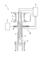
- FIG. 1 is a vertical cross-sectional view showing a magnetized plasmoid injection device according to this embodiment.
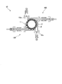
- FIG. 2 is a cross-sectional view showing the magnetized plasmoid injection device in this embodiment.
- reference numeral 10 is a magnetized plasmoid ejection device.
- the magnetized plasmoid injection device 10 has an external electrode 11, an internal electrode 12, a plasma generation gas supply unit 13, a power supply control unit 14, and a bias coil (magnetic field generation unit). 15, an impurity generation unit 100, and a magnetic flux holding unit (not shown).
- the external electrode 11 is made of, for example, a cylindrical conductor. Further, the internal electrode 12 is arranged coaxially with the external electrode 11. An annular magnetized plasmoid generating space is formed between the outer electrode 11 and the inner electrode 12.
- the space inside the cylindrical outer electrode 11 in the radial direction and outside the cylindrical inner electrode 12 in the radial direction is the annular magnetized plasmoid generation space.
- the cylindrical surface of the external electrode 11 and the cylindrical surface of the internal electrode 12 form an annular magnetized plasmoid generating space so that they have the same radial separation distance from each other in the entire circumferential direction.
- one end of the external electrode 11 is connected to the flange 11a.
- One end of the internal electrode 12 extends to the outside of one end of the external electrode 11.
- One end of the internal electrode 12 is connected to the flange 12a.
- the flange 11a and the flange 12a are arranged coaxially.
- the flange 11a and the flange 12a are arranged apart from each other in the axial direction.
- the positions of the outer electrode 11 and the inner electrode 12 are fixed by a flange 11a and a flange 12a.
- the inner diameter of the flange 11a is the same as that of one end of the cylindrical outer electrode 11.
- the flange 11a is an annular plate body extending outside the external electrode 11.
- the inner diameter of the flange 12a is the same as one end of the cylindrical inner electrode 12.
- the flange 12 a is an annular plate body extending outside the internal electrode 12.
- the flange 11a and the flange 12a are separated from each other so that their facing surfaces are parallel to each other.
- the flange 11a and the flange 12a are connected to each other by a cylindrical member 17.
- the cylindrical member 17 has an annular insulating member 18 arranged at an intermediate position between the flange 11a and the flange 12a.
- the insulating member 18 insulates both ends of the cylindrical member 17.
- the flange 11a and the flange 12a are insulated by the insulating member 18.
- a space between the flange 11a and the flange 12a is surrounded by a cylindrical member 17 and an insulating member 18, which are circumferential surfaces.
- the space between the flange 11a and the flange 12a can be sealed in a vacuum state through the cylindrical member 17 and the insulating member 18.
- a space that is inside of the cylindrical member 17 and the insulating member 18 in the radial direction and outside of the internal electrode 12 in the radial direction communicates with an annular magnetized plasmoid generating space formed between the external electrode 11 and the internal electrode 12. ing.
- the external electrode 11 has an open end so that plasma is emitted from the other end.
- the outer electrode 11 and the inner electrode 12 are preferably formed of a material that is not magnetized, has a high melting point, and is easily processed. For example, it may be made of stainless steel or the like.
- the other end of the internal electrode 12 is closed in a closed state.
- a bias coil 15 is arranged inside the internal electrode 12.
- the nozzle 13 a of the plasma generation gas supply unit 13 is connected to the outer peripheral position of the external electrode 11.
- the plasma generation gas supply unit 13 is connected to the nozzle 13 a so as to supply the plasma generation gas to the annular magnetized plasmoid generation space formed between the outer electrode 11 and the inner electrode 12.
- the plasma generation gas supply unit 13 can supply a plasma generation gas, such as hydrogen gas, helium gas, or argon gas, to the nozzle 13a.
- a plasma generation gas such as hydrogen gas, helium gas, or argon gas
- the nozzle 13a is provided with respect to an annular magnetized plasmoid generating space formed by the external electrode 11 and the internal electrode 12 in a plane orthogonal to the axes of the external electrode 11 and the internal electrode 12. It is arranged so that the tangential direction is the gas ejection direction. That is, the nozzle 13 a opens in the annular magnetized plasmoid generating space so as to penetrate the external electrode 11 from the outside, and in the annular magnetized plasmoid generating space, the outer periphery of the internal electrode 12 is in the circumferential direction of the internal electrode 12. The plasma generation gas is jetted so as to flow to the.
- the nozzle 13a opens toward the inside of the external electrode 11 so as to penetrate the external electrode 11 from the outside.
- the nozzle 13 a ejects the plasma generation gas into the external electrode 11.
- the outer electrode 11 and the inner electrode 12 form an annular magnetized plasmoid generating space between the outer electrode 11 and the inner electrode 12 on an axis orthogonal plane orthogonal to the axes of the outer electrode 11 and the inner electrode 12.
- the magnetization plasmoid generation space has substantially the same cross-sectional shape in the axial direction of the external electrode 11 and the internal electrode 12.
- the nozzle 13a ejects a plasma generating gas in a tangential direction to an annular magnetized plasmoid generating space in the plane orthogonal to the axis.
- the nozzle 13a ejects the plasma generating gas to the outside of the periphery of the internal electrode 12 in the plane orthogonal to the axis.
- the nozzle 13a ejects the plasma generating gas in the tangential direction of the internal electrode 12 on the plane orthogonal to the axis.
- the nozzle 13a ejects the plasma-producing gas along the plane orthogonal to the axis.
- the nozzle 13a is provided on the plane orthogonal to the axes of the external electrode 11 and the internal electrode 12 with respect to the annular magnetized plasmoid generating space formed by the external electrode 11 and the internal electrode 12. It is installed at two places so as to be at both ends in the radial direction of 11.
- the two nozzles 13a are set to be in parallel with each other, and the ejection directions of the plasma generating gas are opposite to each other.
- the two nozzles 13a are set such that the distance between them in the plane orthogonal to the axis is substantially equal to the diameter dimension of the annular magnetized plasmoid generating space.
- the distance between the two nozzles 13 a in the plane orthogonal to the axis is set to be smaller than the diameter dimension of the external electrode 11.
- the distance between the two nozzles 13 a in the plane orthogonal to the axis is set to be larger than the diameter dimension of the internal electrode 12.
- the distance between the two nozzles 13a on the axis-orthogonal plane is defined as the distance along the axis-orthogonal plane and in the direction orthogonal to the axis of the two nozzles 13a.
- the two nozzles 13a can have the same opening size.
- the opening size of the nozzle 13a may be set to be substantially equal to or smaller than the radial distance between the cylindrical surface of the external electrode 11 and the cylindrical surface of the internal electrode 12.
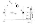
- FIG. 3 is a cross-sectional view showing an impurity generation unit in the magnetized plasmoid injection device in this embodiment.
- the impurity generation unit 100 has a needle electrode 101 made of an impurity contained in the magnetization plasmoid.
- the needle-shaped electrode 101 is located inside the cylindrical cover electrode 102.
- the cover electrode 102 is connected so that one end thereof opens to the external electrode 11.
- the needle electrode 101 is made of a conductive material such as a heavy metal such as tungsten, molybdenum, or gold contained as an impurity in the magnetized plasmoid, or a single substance such as carbon, chromium, niobium, or fluorine contained in the magnetized plasmoid as a film-forming material. It can consist of these compounds.
- Table 1 shows examples of the types of impurities (impurity elements) contained in the needle-shaped electrode 101, the formation state as the needle-shaped electrode 101 (needle-shaped electrode state), and its use.
- the cover electrode base 104 is connected to the other end of the cover electrode 102.
- the base end of the needle electrode 101 is connected and fixed to the cover electrode base 104.
- the cover electrode 102 has a cylindrical insulating member 103 between one end and the other end. ing.
- the insulating member 103 connects one end of the cover electrode 102 opening to the external electrode 11 and the cover electrode base 104 in an insulated state.
- the needle electrode 101 is arranged in the center with respect to the cover electrode 102, the insulating member 103, and the cover electrode base 104 so as to coincide with the axes thereof.
- the cover electrode 102, the insulating member 103, and the cover electrode base 104 are all separated from the needle electrode 101, and the insides thereof are hermetically sealed so that the pressure can be reduced in vacuum.
- the separation portion 105 to which the base end of the needle electrode 101 is connected and fixed is separable from the cover electrode 102.
- the proximal end of the needle-shaped electrode 101 may be connected to the separated portion 105 using a crimp terminal.
- the base end of the needle-shaped electrode 101 can be connected to the separation portion 105 by adopting crimping using a crimping terminal or a set screw.
- the impurity generation part 100 separates the separation part 105 and the needle electrode 101 from the cover electrode base 104 side by separating the separation part 105 from the cover electrode 102, the insulating member 103, and the cover electrode base 104. Is possible.
- the cover electrode base portion 104 and the separation portion 105 can be hermetically sealed when they are connected to each other.
- the inner diameter dimension of the cover electrode 102 opening to the outer electrode 11 is set to be substantially equal to or smaller than the radial distance (spacing) between the outer electrode 11 and the inner electrode 12. That is, the opening size in the cover electrode 102 may be set to be substantially equal to or smaller than the radial distance between the cylindrical surface of the external electrode 11 and the cylindrical surface of the internal electrode 12.
- the impurity generation unit 100 has a ring-shaped magnetized plasmoid generation space formed by the external electrode 11 and the internal electrode 12 in a plane orthogonal to the axes of the external electrode 11 and the internal electrode 12,
- the external electrodes 11 are installed at two positions so as to be at both ends in the radial direction.
- the two impurity generating portions 100 are set in parallel with each other and the tips of the needle electrodes 101 are opposite to each other.
- a plurality of the impurity generation units 100 are arranged so as to be orthogonal to the nozzles 13a on the surface orthogonal (intersecting) to the axes of the external electrode 11 and the internal electrode 12.
- the arrangement of the cover electrode 102 and the arrangement of the nozzles 13a can be made point-symmetrical in the plane orthogonal to the axis. That is, the cover electrode 102 and the nozzle 13 a can be arranged symmetrically with respect to the axes of the external electrode 11 and the internal electrode 12.
- the cover electrode 102 is opened toward the inside of the external electrode 11 so as to penetrate the external electrode 11 from the outside.
- the axial directions of the cover electrode 102 and the needle electrode 101 are arranged along the tangential direction of the annular magnetized plasmoid generating space in the plane orthogonal to the axis.
- the needle-shaped electrode 101 is located radially outside around the internal electrode 12 in the plane orthogonal to the axis.
- the needle electrode 101 is located in the tangential direction of the internal electrode 12 in the plane orthogonal to the axis.
- the tip of the needle-shaped electrode 101 does not protrude to the inner electrode 12 side outside the magnetized plasmoid generation space, that is, to the inner electrode 12 side beyond the cylindrical surface that extends the surface of the outer electrode 11 that has a cylindrical shape at the opening of the cover electrode 102. Can be position.
- the needle electrode 101 is arranged so as to project inside the magnetized plasmoid generation space from the external electrode 11 or at a position outside the magnetized plasmoid generation space from the external electrode 11, that is, the cover electrode base 104 side. It is also possible to set the position to be the position.
- An impurity generation power supply is connected to the impurity generation unit 100.
- the impurity generation power source is connected to the cover electrode 102 and the cover electrode base 104 and sputters only the needle electrode 101, so that a crowbar circuit using a diode can be formed.
- the function of the impurity generation power supply is contained in the power supply control unit 14.
- the crowbar circuit connects a circuit having a power source V1 and a circuit having a capacitor C02 in parallel, and these circuits are connected via an ignitron IT (switch element).
- the circuit of the bypass diode D03 and the cover electrode 102 and the cover electrode base 104 which are loads are connected in parallel.
- the circuit of the capacitor C02 is a crowbar circuit, and the capacitor C02 is a crowbar capacitor.
- the capacitor C02 is a charging capacitor.
- the crowbar circuit shown in FIG. 3 is an example, and it is not limited to this configuration as long as a sputter voltage capable of diffusing impurities from the needle electrode 101 can be applied to the pulse drive of the bias coil 15 described later. ..
- the power supply control unit 14 has a plasma power supply (power supply circuit), a bias coil pulse power supply, an impurity generation power supply, and a control unit for controlling these.
- the plasma power supply (power supply circuit) in the power supply control unit 14 applies a load signal between the external electrode 11 and the internal electrode 12.
- the plasma power supply (power supply circuit) may be, for example, one that applies a load signal in the form of direct current, or one that applies a continuous pulse signal.
- the load signal means a load voltage applied between the outer electrode 11 and the inner electrode 12, or a load current flowing at that time.
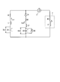
- FIG. 4 is a circuit diagram showing an example of a plasma power supply (power supply circuit) in the magnetized plasmoid injection device according to the present embodiment.
- the plasma power supply (power supply circuit) has a circuit of a capacitor C1, an inductance L1, and a resistor R1 connected in parallel with a circuit of a capacitor C2 having a bypass diode D2 connected in parallel, an inductor L2, a resistor R2, and a diode D1.
- the circuit of is connected to the load F via an ignitron IT (switch element).
- Circuits such as the diode D1 and the capacitor C2 are power crowbar circuits, the diode D1 is a crowbar switch, and the capacitor C2 is a power crowbar capacitor.
- the capacitors C1 and C2 are charging capacitors.
- the capacitors C1 and C2 are used so that their capacities are C1 ⁇ C2, that is, the capacitor C2 has a larger capacity than the capacitor C1.
- the voltages Vc1 and Vc2 of the capacitors C1 and C2 are charged with the same polarity so that Vc1> Vc2, that is, the voltage Vc1 of the capacitor C1 becomes higher than the voltage Vc2 of the capacitor C2.
- the diode D1 becomes non-conductive with respect to the voltage Vc1 of the capacitor C1, so the capacitor C2 is not discharged.
- the diode D1 conducts, the capacitor C2 starts discharging, and the discharge current Ic2 of the capacitor C2 flows into the load F.
- the load current IL flows through the diode D2 and returns. Therefore, the load current IL becomes a non-oscillating unipolar damping current.
- the power crowbar circuit shown in FIG. 4 can supply a load current having a steep rise and a gradual attenuation, and can continuously generate a plasma lump by one charge.
- the power crowbar circuit shown in FIG. 4 uses a capacitor C1 having a small capacity and a capacitor C2 for a power crowbar having a large capacity, and makes the charging voltage of the capacitor C1 higher than the charging voltage of the capacitor C2.
- the discharge current of the capacitor C1 contributes, and thereafter the discharge current of the capacitor C2 mainly contributes, so that the load current has a steep rise and a gradual attenuation.
- a diode D1 is used for the crowbar switch, and when the discharge voltage of the capacitor C1 becomes lower than the charge voltage of the capacitor C2, the diode D1 automatically conducts and starts discharging the capacitor C2.
- the Ignitron IT can use other semiconductor switches that can switch between conducting and non-conducting under the control of the control unit instead of the Ignitron.
- the ignitron IT may be connected in series with the resistor R1 and closer to the resistor R1 than the connection point of the diode D1. The smaller the resistances R1 and R2, the smaller the loss, and the smaller the inductances L1 and L2, the smaller the pulsation of the load current IL.
- the inductance L1 is made larger than the inductance L2, the return of the load current IL to the capacitor C1 becomes small, and most of the load current IL flows through the power crowbar circuit.
- the pulse coil pulse power supply in the power supply control unit 14 drives the bias coil 15 in a pulsed manner.
- the bias coil pulse power supply is configured to be able to apply, for example, a sine wave current having a predetermined frequency to the bias coil 15.
- a transistor may be used to control the power source (capacitor) by an inverter, and a rectangular pulse continuous pulse signal may be applied to the bias coil 15.
- control unit in the power supply control unit 14 controls the bias coil pulse power supply so as to pulse-drive the bias coil 15, and outputs between the external electrode 11 and the internal electrode 12 from the plasma power supply (power supply circuit). It controls the additional signal and the impurity generation power supply.
- the bias coil 15 is arranged inside the internal electrode 12. As a result, baking of the vacuum container, which is essential for obtaining an ultrahigh vacuum, is possible without being affected by the bias coil. Therefore, the adsorbed gas can be removed.
- the bias coil 15 applies a bias magnetic field to the plasma generated between the external electrode 11 and the internal electrode 12. As a result, the plasma is emitted in a state in which the magnetic field due to the discharge current and the bias magnetic field are included, so that spheromak plasma is generated.
- the control unit in the power supply control unit 14 has a sufficient time for the bias magnetic field required for generating the spheromak plasma to be applied between the external electrode 11 and the internal electrode 12, and for the bias magnetic field to the magnetic flux holding unit.
- the bias coil pulse power supply is controlled so that the bias coil 15 is pulse-driven in a time shorter than the magnetic flux soak time. That is, the spatial distribution of the magnetic flux of the bias magnetic field is controlled at a time interval that does not allow the magnetic flux to soak into the magnetic flux holding portion, and control is performed so that the necessary bias magnetic field is efficiently generated between the external electrode 11 and the internal electrode 12. ..
- the magnetic flux holding unit is used to prevent the magnetic flux of the bias magnetic field applied by the bias coil 15 from leaking to the outside.
- the magnetic flux holding portion is formed integrally with the external electrode 11. That is, the external electrode 11 is made of a material having high conductivity and low magnetic permeability, such as copper, and the thickness of the external electrode 11 is longer than the time required for the bias magnetic field and the time for the magnetic flux to soak into the magnetic flux holding portion. It is designed to be thick enough for shorter time.
- the magnetic flux holder may be configured to be attachable to and detachable from the external electrode 11. With this, it is possible to change the thickness of the magnetic flux holding portion according to plasma generation conditions and the like.
- the magnetic flux holding portion is formed in conformity with the outer shape of the external electrode 11. For example, if the external electrode 11 has a cylindrical shape, the magnetic flux holding portion also has a cylindrical shape accordingly. Then, the magnetic flux holding portion is configured to cover the outer electrode 11 in a jacket shape or a shell shape.
- the magnetic flux holding portion is made of a material having high conductivity and low magnetic permeability. For example, copper or a copper alloy may be used. If the length of the magnetic flux holding portion is equal to or longer than the length of the bias coil 15, the magnetic flux of the bias magnetic field generated from the bias coil 15 can be efficiently confined.
- the thickness of the magnetic flux holding portion even if the bias coil 15 is driven for a sufficient time so that the bias magnetic field required for generating the spheromak plasma is applied between the external electrode 11 and the internal electrode 12, It has a thickness that prevents magnetic flux from penetrating the holding part and passing through it.
- the magnetic flux When the magnetic flux is applied to the magnetic flux holding section for a long time, it penetrates into the magnetic flux holding section and passes through it.Therefore, it is longer than the time required for the bias magnetic field, and considering the time for the magnetic flux to soak and the thickness of the magnetic flux holding section, Set the drive time.
- the control unit in the power supply control unit 14 controls the impurity generation power supply to apply a voltage to the needle electrode 101 of the impurity generation unit 100 to diffuse the impurities into the magnetization plasmoid generation space and control the bias coil pulse power supply. Then, the plasma power supply (power supply circuit) is controlled in a state where the bias magnetic field necessary for generating the spheromak plasma is applied between the external electrode 11 and the internal electrode 12, and the external electrode 11 and the internal electrode 12 are controlled. And a discharge voltage is applied between and.
- the control unit in the power supply control unit 14 applies a bias magnetic field at the same time as or before or after applying a voltage to the needle electrode 101, and then applies a discharge voltage between the external electrode 11 and the internal electrode 12. By doing so, impurities are contained in the generated plasma.
- the timing of voltage application or bias magnetic field application to the needle-shaped electrode 101 is set according to each pulse discharge and the time scale of diffusion of the impurity element, so that the generated plasma contains impurities.
- FIG. 5 is a horizontal cross-sectional view showing an impurity diffusion state in the magnetized plasmoid injection device in the present embodiment
- FIG. 6 is a vertical cross-sectional view showing a plasma generation state in the magnetized plasmoid injection device in the present embodiment
- FIG. 4 is a transverse cross-sectional view showing a plasma generation state in the magnetized plasmoid injection device in the present embodiment.
- the plasma generation gas is supplied from the plasma generation gas supply unit 13.
- the plasma generating gas is ejected from the nozzle 13a in the tangential direction of the magnetized plasmoid generating space between the outer electrode 11 and the inner electrode 12 which are annular. This stabilizes the flow of the plasma generation gas in the magnetized plasmoid generation space, and also makes the introduced gas density spatially uniform.
- control unit in the power supply control unit 14 controls the impurity generation power supply to apply a voltage to the needle-shaped electrode 101 of the impurity generation unit 100 to diffuse the impurities into the magnetization plasmoid generation space as shown in FIG. ..
- the range in which the impurities diffuse in the magnetized plasmoid generation space is equal to or more than the range in which plasma is generated in the region around the nozzle 13a in the axial direction of the external electrode 11 and the internal electrode 12, for example. It is preferably set to be small.
- the impurity diffusion range can be controlled by, for example, setting the gas introduction time, the discharge in the impurity generation unit 100, the discharge timing in the magnetization plasmoid generation unit, and the like.
- the timing of the discharge of the magnetization plasmoid generator is set by the pulse coil pulse power supply and the plasma power supply (power supply circuit).
- the control unit in the power supply control unit 14 controls the bias coil pulse power supply to generate a bias magnetic field required for generating spheromak plasma between the external electrode 11 and the internal electrode 12.
- the plasma power supply (power supply circuit) is controlled to apply a discharge voltage between the external electrode 11 and the internal electrode 12 while being applied between the electrodes.
- the plasma power supply power supply circuit
- FIG. 7 a discharge current flows and plasma P is generated.
- the bias magnetic field generated by the bias coil 15 is spatially distributed controlled by the bias coil pulse power supply, the magnetic flux holding unit, and the control unit, and the magnetic flux is dispersed in the plasma generation region.
- the generated plasma P generates magnetic fields in the poloidal direction and the toroidal direction due to the magnetic field generated by the discharge current and the bias magnetic field generated by the bias coil 15, and is emitted from the open ends of the external electrode 11 and the internal electrode 12 as spheromak plasma.
- the released spheromak plasma does not immediately diffuse and is released at a high speed in the state of a plasma lump.
- the generated plasma P may contain the diffused impurities at a predetermined concentration and concentration distribution. it can.
- the needle electrode 101 is installed in the vicinity of the nozzle 13a serving as the gas introduction point, and the impurities are diffused at the same time when the bias magnetic field is formed. Therefore, it is preferable that the ionized impurity element is set to be trapped in the plasma P.
- the plasma generating gas is supplied from the nozzle 13a in the tangential direction of the magnetized plasmoid generating space.
- the magnetized plasmoid emitting device 10 can generate stable plasma in a neutral state.
- the impurity generation unit 100 is provided in the tangential direction of the magnetized plasmoid generation space on the same plane as the nozzle 13a.
- the magnetized plasmoid injection device 10 of the present embodiment can easily remove the ionized impurities. It becomes possible to make it contain in plasma.
- the magnetized plasmoid injection device 10 of the present embodiment can improve the stability of the generated plasma.
- the magnetized plasmoid injection device 10 of the present embodiment supplies impurities to the magnetized plasmoid generating space by sputtering the needle electrode 101. Therefore, the magnetized plasmoid injection device 10 according to the present embodiment facilitates precise control of the amount of impurities generated by sputtering. Therefore, the magnetization plasmoid injection device 10 according to the present embodiment can set the impurity concentration contained in the magnetization plasmoid extremely accurately.
- the needle-like electrode 101 can be replaced or a predetermined needle-like electrode 101 can be attached in advance to make impurities into desired types.
- the magnetization plasmoid injection device 10 of the present embodiment can control the amount and composition ratio of the impurities contained in the plasma for a very short time, that is, for each magnetization plasmoid unit generated in a pulse shape. ..
- the magnetized plasmoid generator 10 of the present embodiment can easily set temporal changes in the amount of impurities contained and the composition ratio in the plasma to be emitted.
- the magnetization plasmoid injection device 10 of the present embodiment supplies impurities from the impurity generation unit 100, and the generated magnetization plasmoid advances in the magnetization plasmoid generation space formed by the external electrode 11 and the internal electrode 12 and is emitted. During the heating, the impurities are uniformly contained in the magnetized plasmoid. As a result, the magnetization plasmoid emitting device 10 of the present embodiment can generate and emit a magnetization plasmoid having a uniform impurity concentration according to the axial length of the magnetization plasmoid generation space.
- the magnetized plasmoid injection device 10 of this embodiment can switch between a state in which the needle electrode 101 is not sputtered and a state in which the needle electrode 101 is sputtered.
- the magnetized plasmoid injection device 10 of the present embodiment can switch between the plasma containing no impurities and the plasma containing impurities to generate the plasma for a predetermined time.
- the impurity generation unit 100 is provided in the tangential direction of the magnetized plasmoid generation space, so that the impurities generated from the needle-shaped electrode 101 adhere to the surface of the internal electrode 12 extremely. It becomes possible to reduce.
- the magnetized plasmoid injection device 10 of the present embodiment can reduce the occurrence of defects such as deposits on the surface of the internal electrode 12 due to the plasma generation gas supplied from the nozzle 13a.
- the type of impurities can be changed only by exchanging the needle-shaped electrode 101 in the impurity generation unit 100, so that the entire magnetization plasmoid generation space is opened and exchanged. There is no need, and it is possible to reduce adverse effects such as external contamination on the inside of the device. As a result, the magnetized plasmoid injection device 10 according to the present embodiment can reduce the work steps in the maintenance of the device and reduce the maintenance time.
- the magnetized plasmoid injection device 10 immediately after the impurities are generated from the impurity generator 100 in the magnetized plasmoid generation space, the bias magnetic field is formed and the plasma discharge is generated between the external electrode 11 and the internal electrode 12.
- the present invention is not limited to this. If the plasma generating gas can be supplied between the outer electrode 11 and the inner electrode 12, for example, a plasma generating gas supply unit may be provided inside the inner electrode 12 in the radial direction.
- the nozzle 13a of the plasma generation gas supply unit 13 and the impurity generation unit 100 are opened in the external electrode 11 at different positions.
- the impurity generation portion 100 and the nozzle can be used together. In this case, it is possible to increase the amount of impurities supplied to the magnetization plasmoid generation space to generate magnetization plasmoids having an increased impurity concentration.
- the magnetized plasmoid injection device 10 of the present embodiment supplies the plasma-producing gas near the center of the bias coil 15, but in this case, the efficiency for increasing the magnetic flux contained in the magnetized plasmoid becomes the best.
- the nozzle 13a of the plasma generating gas supply unit 13 is provided so as to penetrate a part of the magnetic flux holding unit that covers the outside of the external electrode 11 as in the present embodiment.
- the magnetized plasmoid injection device 10 of the present embodiment two nozzles 13a of the plasma generation gas supply unit 13 and two impurity generation units 100 are opened in the external electrode 11, but the present invention is not limited to this. .. It is also possible to provide a plurality of three or more. In this case, the nozzle 13a and the impurity generation unit 100 can be provided in the tangential direction of the cylindrical magnetized plasmoid generation space.
- the nozzles 13a of the plurality of plasma generation gas supply units 13 and the impurity generation unit 100 are arranged in the same plane intersecting the axis of the magnetized plasmoid generation space. Can also be arranged so that they are located in parallel planes in which the axial positions of the magnetization plasmoid generation space are different.
- the nozzles 13a of the plurality of plasma generation gas supply units 13 and the impurity generation unit 100 may be arranged in a direction different from the direction along the plane orthogonal to the axis. Even in this case, the impurity generation unit 100 and the nozzle 13a can be provided in the tangential direction of the cylindrical magnetized plasmoid generation space.
- any one of the plurality of impurity generators 100 and the nozzles 13a provided respectively, or a plurality of appropriately selected ones, is provided in a direction other than a plane orthogonal to the axes of the external electrode 11 and the internal electrode 12. As a state of being along, it can be arranged in a plane intersecting at an angle. Even in this case, the impurity generation unit 100 and the nozzle 13a can be provided in the tangential direction of the cylindrical magnetized plasmoid generation space. Note that the impurity generation unit 100 may not be provided.
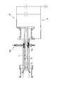
- FIG. 8 is a schematic diagram showing the magnetic confinement plasma device according to this embodiment.
- the present embodiment is different from the above-described first embodiment in that it relates to a portion that emits a magnetization plasmoid, and other configurations corresponding to those in the above-described first embodiment are denoted by the same reference numerals. The description is omitted.
- the magnetic confinement plasma device 20 has a magnetized plasmoid emission device 10 and a magnetic confined plasma part 21 as a portion from which the magnetized plasmoid emission device 10 emits plasma.
- the magnetic confinement plasma unit 21 is, for example, a core of a nuclear fusion reactor, and a magnetized plasmoid including an element serving as a tracer is incident by the magnetized plasmoid injection device 10.
- the magnetic confinement plasma part 21 can analyze the behavior of the plasma in the furnace by a spectroscope or the like, for example, by using a magnetized plasmoid containing the ejected element.
- the magnetically confined plasma unit 21 is composed of a port required for plasmoid injection, a coil for forming a confined magnetic field, a power supply required for generating target plasma, a vacuum pump, and the like.
- the needle electrode 101 at one location may be made of a conductive material, and a compound or alloy may be used.
- the needle-shaped electrode 101 is composed of one or more elements selected from W, Sn, Nd, Sm, Gd, Tb, Dy, Er, Yb, Au, Pb, Bi, Ti, Cu, C, Al and Mo.
- a plurality of impurity generation units 100 having these needle-shaped electrodes 101 can be provided.
- the magnetic confinement plasma device 20 of the present embodiment it is possible to supply impurities, which were difficult to be contained conventionally, to the magnetic confinement plasma portion 21 in the furnace, and observe and measure the behavior thereof by a spectroscope or the like. It will be possible.
- the magnetic confinement plasma device 20 of the present embodiment is capable of supplying the magnetized plasmoid containing the element serving as the tracer, so that the plasma energy of the plasma energy in the magnetic confinement plasma portion 21 generated by supplying the solid is reduced. It becomes possible to supply the tracer element while preventing decrease (local cooling of plasma). This makes it possible to minimize changes in the behavior of the plasma in the magnetically confined plasma portion 21 and supply the tracer element.
- the magnetic confinement plasma device 20 of the present embodiment can supply the magnetized plasmoid containing the tracer element without causing this problem.
- the magnetic confinement plasma device 20 of this embodiment includes the impurity generation unit 100, it becomes easy to precisely control the amount of the tracer element contained in the ejected magnetized plasmoid. As a result, in the magnetic confinement plasma device 20 of this embodiment, it is possible to set the amount of the element serving as the tracer to be supplied to the plasma of the magnetic confinement plasma unit 21 extremely accurately.
- the magnetic confinement plasma device 20 of the present embodiment supplies the plasma of the magnetic confinement plasma unit 21 by exchanging the needle electrode 101 of the impurity generation unit 100 or by attaching a predetermined needle electrode 101 in advance.
- the tracer element can be of a desired type, or a plurality of types of tracer elements can be supplied at the same time.
- the magnetic confinement plasma device 20 according to the present embodiment is configured to generate an amount and composition ratio of elements serving as a tracer to be supplied to the plasma of the magnetic confinement plasma unit 21 in a very short time, that is, in a pulsed form and emit the magnetization. It becomes possible to control for each plasmoid unit.
- the magnetic confinement plasma device 20 of the present embodiment can also set the temporal changes in the amount of elements and the composition ratio that serve as a tracer to supply the plasma of the magnetic confinement plasma unit 21.
- the magnetized plasmoid ejecting device 10 can supply the magnetized plasmoid containing an element which becomes a uniform tracer in advance to the plasma of the magnetic confined plasma part 21.
- the magnetic confinement plasma device 20 of the present embodiment can improve the homogenization of the tracer element in the magnetic confinement plasma part 21.
- the magnetic confinement plasma device 20 of the present embodiment switches between the state in which the needle electrode 101 of the impurity generation unit 100 is not sputtered and the state in which the needle electrode 101 is sputtered, and the presence or absence of the tracer element is selected to magnetize. It is also possible to supply the plasmoid to the plasma of the magnetically confined plasma part 21.
- the magnetic confinement plasma device 20 of this embodiment since the impurity generation unit 100 is provided in the tangential direction of the magnetized plasmoid generation space, it is extremely difficult for impurities generated from the needle-shaped electrode 101 to adhere to the surface of the internal electrode 12. It becomes possible to reduce. At the same time, the magnetic confinement plasma device 20 of the present embodiment can reduce the occurrence of defects such as deposits on the surface of the internal electrode 12 due to the plasma generation gas supplied from the nozzle 13a. Further, in the magnetic confinement plasma device 20 of the present embodiment, the type of tracer element can be changed only by replacing the needle electrode 101 in the impurity generation unit 100.
- the magnetic confinement plasma device 20 of the present embodiment it is not necessary to open and replace the entire region of the magnetized plasmoid generating space of the magnetized plasmoid ejecting device 10 and the magnetic confined plasma part 21 that communicates with the magnetized plasmoid generator space, and to the outside of the device. It is possible to reduce adverse effects such as pollution from the. As a result, the magnetic confinement plasma device 20 of the present embodiment can reduce the work steps for maintenance of the device and shorten the maintenance time.
- the nozzle 13 a of the plasma generation gas supply unit 13 and the impurity generation unit 100 in the magnetized plasmoid injection device 10 are opened in the external electrode 11, respectively. It is also possible to supply the plasma generating gas from the base side of the above and also serve as the nozzle. In this case, the magnetic confinement plasma device 20 of this embodiment can increase the amount of the tracer element contained in the magnetization plasmoid supplied to the magnetic confinement plasma unit 21. As a result, in the magnetic confinement plasma device 20 of the present embodiment, when a tracer element such as tungsten is mixed, gas is also supplied from the impurity generation unit 100 serving as a tracer introduction electrode unit, and the needle electrode 101 is not charged. By discharging at a high pressure, it is possible to increase the sputtering efficiency by ion bombing and increase the tracer element amount.
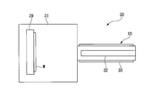
- FIG. 9 is a schematic diagram showing the plasma processing apparatus in this embodiment.
- the present embodiment is different from the above-described first and second embodiments in that the film is formed by the emitted magnetized plasmoid, and other corresponding components are denoted by the same reference numerals. The description is omitted.
- the plasma processing apparatus 30 of the present embodiment is configured to perform plasma processing, for example, film formation processing, on the substrate W to be processed using plasma emitted from the magnetization plasmoid emitting apparatus 10.
- the plasma processing apparatus 30 of the present embodiment is connected to the internal electrode 32 made of a film forming material, the bias coil 35 located outside the external electrode 11, and the magnetization plasmoid injection device 10 to be magnetized. It has a processing chamber 31 into which a plasmoid is emitted, and a stage (processing substrate holding unit) 39 that is arranged in the processing chamber 31 and holds a substrate to be processed.
- the internal electrode 32 corresponds to the internal electrode 12 in the above-described embodiment and is formed in a columnar shape made of a film forming material.
- the film forming material for the internal electrodes 32 may be metal, carbon, or a conductive compound or mixture containing them.
- the substrate W to be film-formed includes various substrates such as a silicon substrate, an aluminum substrate, PET (polyethylene terephthalate), and the like.
- the carbon ions are accelerated by the Lorentz force due to the discharge current and are incident on the substrate W to be processed, so that the potential control of the substrate W to be processed is not necessarily required. Therefore, it is possible to form a film on a dielectric material or the like for which the potential control is difficult. Further, the plasma processing apparatus 30 of the present embodiment does not require potential control for the substrate to be processed W, and is therefore advantageous when it is difficult to apply a potential to the substrate to be processed W individually in line production, for example.
- the plasma processing apparatus 30 of the present embodiment since the emitted spheromak plasma has a low heat load, a DLC (Diamond-Like Carbon) thin film or the like can be formed even if the substrate W to be processed is weak to heat. Is. Further, the hardness of the produced DLC thin film becomes higher by increasing the collision energy. Therefore, the plasma processing apparatus 30 of the present embodiment can positively apply the potential to the substrate W to be processed if the potential can be applied to increase the collision energy and increase the hardness.
- a DLC Diamond-Like Carbon
- the processing chamber 31 is sealed by satisfying predetermined film forming conditions.
- the structure of the processing chamber 31 is not particularly limited as long as plasma processing can be performed inside.
- the processing chamber 31 is a vacuum chamber.
- the processing chamber 31 is connected to the magnetized plasmoid injection device 10.
- the processing chamber 31 is configured to receive plasma emitted from the open ends of the outer electrode 11 and the inner electrode 32. Specifically, the processing chamber 31 is connected to the open end of the external electrode 11 via an insulator, and the released plasma is introduced inside.
- the bias coil 35 can be wound so as to surround the outer circumference of the external electrode 11.
- the bias coil 35 applies a vertical magnetic field between the external electrode 11 and the internal electrode 32 to extend an effective inter-electrode distance in order to promote dielectric breakdown.
- the bias coil 35 applies a bias magnetic field to the plasma generated between the outer electrode 11 and the inner electrode 32. Due to the function of these bias coils 35, plasma is emitted in a state including a magnetic field due to a discharge current and a bias magnetic field. Therefore, due to the function of the bias coil 35, an isolated magnetization plasmoid having a spheromak-like magnetic field structure is generated and filtered by the magnetic field.
- the stage 39 is fixed in the processing chamber 31.
- the stage 39 holds the surface of the substrate W to be processed on which the film is to be formed so as to face it in a direction perpendicular to the axial direction of the internal electrode 32.
- the stage 39 may be configured so that the distance between the magnetized plasmoid emitting device 10 and the substrate W to be processed can be continuously changed. Further, the stage 39 may be grounded or set to a negative voltage so as to draw plasma ions to the stage 39 side. In this case, the processing chamber 31 and the stage 39 may be insulated.
- the stage 39 can be arranged so that the center of the magnetized plasmoid emitting device 10 and the center of the substrate W to be processed coincide with each other.
- plasma generation gas for example, argon gas is supplied from the plasma generation gas supply unit 13 to the magnetization plasmoid generation space.
- the impurity generation unit 100 also supplies impurities to the magnetization plasmoid generation space.
- a bias coil 35 applies a vertical magnetic field between the external electrode 11 and the internal electrode 32.
- the effective distance between the electrodes is increased, the dielectric breakdown is promoted, and the plasma is discharged.
- a discharge voltage between the external electrode 11 and the internal electrode 32 discharge is generated between the external electrode 11 and the internal electrode 32 to generate plasma.
- a radial current flows in the plasma.
- a toroidal magnetic field is generated in the plasma by the current of the internal electrode 32.
- the surface of the internal electrode 32 made of the film-forming material is scraped off and mixed into the plasma.
- the Lorentz force due to the radial current in the plasma and the magnetic field in the toroidal direction accelerates the axial direction of the internal electrode 32 while dragging the bias magnetic field.
- the bias magnetic field on the tip side of the magnetized plasmoid injection apparatus 10 becomes a poloidal magnetic field, and spheromak plasma is emitted from the open ends of the external electrode 11 and the internal electrode 32. ..
- the spheromak plasma is not diffused immediately, but is released at high speed in the state of plasma lumps. Since the spheromak plasma contains particles (ions) of the film forming material from which the surface of the internal electrode 32 has been scraped off, the spheromak plasma is made to collide with the target substrate W to form a film on the target substrate W. Material particles are deposited.
- the macroparticles ablated from the internal electrodes 32 do not have an electric charge, so they are not subjected to electromagnetic acceleration and do not contribute to film formation as they are.
- the plasma processing apparatus 30 deposits the film-forming material particles containing impurities on the substrate W to be processed until a desired film thickness is obtained, and forms a desired film to be processed. It becomes possible to obtain.
- the plasma processing apparatus 30 of the present embodiment can control the impurity concentration to a predetermined state in the film thickness direction of the film to be formed during film formation on the substrate W to be processed.
- the plasma processing apparatus 30 controls the impurity concentration contained in the generated magnetization plasmoid by the impurity generation unit 100 to a predetermined state, so that the film to be processed on the substrate W to be processed is
- the impurity concentration can be changed in the thickness direction.
- the needle electrodes 101 of the two impurity generation portions 100 are made of different types, and the impurity supply amounts from the two impurity generation portions 100 are individually controlled, so that the film is formed. It is possible to form a film to be processed having different concentration gradients in the thickness direction.
- the plasma processing apparatus 30 does not supply the impurities from the two impurity generation units 100 during the film formation processing time, so that the impurity-free region is formed at the treatment position in the film thickness direction. It can also be formed. In addition, the plasma processing apparatus 30 can also perform film formation containing impurities of a type that could not be conventionally achieved by appropriately selecting the impurities that form the needle-shaped electrode 101.
- the plasma processing apparatus 30 has a predetermined composition regardless of the difficulty of manufacturing the target. It becomes possible to form a film. Further, in the film formation using the target, even when it is difficult to form the composition ratio inclined in the film thickness direction, the plasma processing apparatus 30 can easily realize this.
- the plasma processing apparatus 30 is not affected by defects that occur in the erosion region of the target, particularly cracks of the target, non-uniformity of composition ratio in the target alloy, non-uniformity of ionization / plasmaization, and the like. It is possible to form a film having a predetermined composition.
- the plasma processing apparatus 30 of the present embodiment is provided with the impurity generation unit 100 in addition to the internal electrode 32 made of a film forming material, it is easy to precisely control the amount of impurities contained in the ejected magnetization plasmoid. Become. Accordingly, the plasma processing apparatus 30 can set the amount of impurities contained in the film to be processed formed on the substrate to be processed in the processing chamber 31 extremely accurately.
- the plasma processing apparatus 30 replaces the needle-shaped electrode 101 of the impurity generation unit 100 or attaches a predetermined needle-shaped electrode 101 in advance to form a film to be processed on the substrate to be processed in the processing chamber 31.
- the impurities contained can be of a desired type.
- the plasma processing apparatus 30 can supply a plurality of types of impurities at the same time by replacing the needle-shaped electrode 101 of the impurity generation unit 100 or by attaching a predetermined needle-shaped electrode 101 in advance.
- the plasma processing apparatus 30 causes the amount of impurities contained in the film to be processed formed on the substrate to be processed in the processing chamber 31 and the composition ratio thereof to be generated in a pulsed manner for a very short time, that is, a magnetization plasmoid that is emitted. It becomes possible to control for each unit. Therefore, the plasma processing apparatus 30 can easily set changes in the amount of impurities contained and the composition ratio in the film thickness direction of the film to be processed formed on the substrate to be processed in the processing chamber 31.
- the magnetized plasmoid injecting apparatus 10 allows the magnetized plasmoid containing the impurities that have been homogenized in advance to be contained in the film to be processed formed on the substrate to be processed in the processing chamber 31. it can. As a result, the plasma processing apparatus 30 can improve the uniformity of impurities contained in the target film formed on the target substrate in the processing chamber 31.
- the plasma processing apparatus 30 switches between a state in which the needle electrode 101 of the impurity generation unit 100 is not sputtered and a state in which the needle electrode 101 is sputtered. As a result, the plasma processing apparatus 30 can select the presence or absence of impurities in the film thickness direction and contain the impurities in the film to be processed formed on the substrate to be processed in the processing chamber 31.
- the plasma processing apparatus 30 since the impurity generation unit 100 is provided in the tangential direction of the magnetized plasmoid generation space, it is possible to extremely reduce the adhesion of impurities generated from the needle electrode 101 to the surface of the internal electrode 12. Becomes At the same time, the plasma processing apparatus 30 can reduce the occurrence of defects such as deposits on the surface of the internal electrode 12 due to the plasma generation gas supplied from the nozzle 13a.
- the plasma processing apparatus 30 can change the type of the tracer element only by replacing the needle electrode 101 in the impurity generation unit 100. Therefore, it is not necessary for the plasma processing apparatus 30 to open and replace the entire area of the magnetized plasmoid generating space of the magnetized plasmoid ejecting apparatus 10 and the processing chamber 31 communicating therewith. Therefore, the plasma processing apparatus 30 can reduce adverse effects such as external contamination on the inside of the apparatus. As a result, the plasma processing apparatus 30 can reduce work steps in maintenance of the apparatus and shorten maintenance time.
- the nozzle 13 a of the plasma generation gas supply unit 13 and the impurity generation unit 100 in the magnetized plasmoid injection device 10 are opened in the external electrode 11, respectively. It is also possible to supply the plasma generating gas from the base side and also serve as the nozzle. In this case, the plasma processing apparatus 30 can increase the amount of impurities contained in the target film formed on the target substrate in the processing chamber 31.
- the substrate W to be processed is arranged so as to face the magnetized plasmoid injection device 10, but the substrate W to be processed is inclined with respect to the axial direction of the magnetized plasmoid injection device 10. It can also be Further, in the plasma processing apparatus 30 of the present embodiment, the center of the magnetized plasmoid injecting apparatus 10 and the center of the substrate W to be processed are aligned with each other, but they may be arranged so as not to be aligned with each other.
- the film processing is performed as the plasma processing in the plasma processing apparatus 30, but the plasma processing apparatus 30 may perform other processing using plasma.
- the plasma processing apparatus 30 may perform plasma etching, plasma cleaning, surface modification, or ion implantation, or may be an apparatus capable of performing these switching operations.
- the device of the present invention is not limited to each of the above-described embodiments, and it goes without saying that various changes can be made without departing from the scope of the present invention.
- the configurations of the respective embodiments can be configured partially or in combination.
- the pulse length and voltage of the applied current can control from an operating region in which sputtering (pushing out by ions) is dominant to a region in which evaporation (evaporation by heat) significantly works.
- carbon which has a low sputtering efficiency, is expected to improve the film forming efficiency by emphasizing the evaporation.
- Examples of utilization of the present invention include production of functional diamond-like carbon, production of alloy thin film, production of functionally graded thin film, and injection of tracer element into a fusion device.
Landscapes
- Engineering & Computer Science (AREA)
- Physics & Mathematics (AREA)
- Chemical & Material Sciences (AREA)
- Plasma & Fusion (AREA)
- Analytical Chemistry (AREA)
- Spectroscopy & Molecular Physics (AREA)
- Chemical Kinetics & Catalysis (AREA)
- Materials Engineering (AREA)
- Mechanical Engineering (AREA)
- Metallurgy (AREA)
- Organic Chemistry (AREA)
- Optics & Photonics (AREA)
- General Engineering & Computer Science (AREA)
- High Energy & Nuclear Physics (AREA)
- Plasma Technology (AREA)
- Physical Vapour Deposition (AREA)
Abstract
不純物量の精密な制御を可能とする磁化プラズモイド射出装置(10)であって、円筒状の外部電極(11)と、外部電極の内部に同軸状に配置される内部電極(12)と、外部電極と内部電極との間にプラズマ生成ガスをパルス状に供給するプラズマ生成ガス供給部(13)と、外部電極と内部電極との間に磁化プラズモイドを生成する磁界を印加する磁界発生部(15)と、外部電極と内部電極との間に放電電圧を印加する電源制御部(14)と、磁化プラズモイドに不純物を含有させる不純物生成部(100)と、を具備し、不純物生成部が、外部電極に開口するカバー電極(102)と、カバー電極内に位置し不純物からなる針状電極(101)と、カバー電極と針状電極とに電圧を印加する不純物生成電源と、を有する。
Description
本発明は磁化プラズモイド射出装置に関し、特に不純物を含有する磁化プラズモイドを高速で射出する際に用いて好適な技術に関する。本願は、2018年11月02日に出願された日本国特許出願第2018-207684号について優先権を主張し、その内容をここに援用する。
スフェロマックプラズマを生成する装置として、磁化同軸プラズマ生成装置が知られている。磁化同軸プラズマ生成装置とは、同軸状に配置された外部電極と内部電極との間に電圧を印加し、両電極間に放電を起こさせることでプラズマを生成させるものである。この際、このプラズマにバイアス磁場を印加すると、放電電流による磁場と共に、バイアス磁場を含んだ状態で放出され、スフェロマックプラズマとなる。ここで、スフェロマックプラズマとは、自分自身に流れる電流によってポロイダルとトロイダルの両閉じ込め磁場が発生し、その磁場構造の持つ磁気ヘリシティを保存するように配位を自己組織化するものである。
このような装置は、磁化プラズモイドを容易に秒速数十から数百km程度で射出できることから、磁化プラズモイド高速射出装置として磁場閉じ込めプラズマヘの燃料粒子供給などに利用されている。
このような装置の例として、本発明者らは特許文献1に示すような出願をおこなっている。
このような装置の例として、本発明者らは特許文献1に示すような出願をおこなっている。
また、磁化プラズモイド高速射出装置は、プラズマ生成時の電流によって電極がスパッタリングされる効果を有する。磁化プラズモイド高速射出装置は、このスパッタリング効果を強調して、金属元素などの不純物をプラズモイドヘ混入および射出することで成膜をおこなうこともできる。
このような装置の例として、本発明者らは、高融点金属を含む合金薄膜であっても安価に生成可能な合金薄膜生成装置に関して、特許文献2および特許文献3に示すような出願をおこなっている。
このような装置の例として、本発明者らは、高融点金属を含む合金薄膜であっても安価に生成可能な合金薄膜生成装置に関して、特許文献2および特許文献3に示すような出願をおこなっている。
しかし、特許文献1および特許文献2に記載された装置では、磁化プラズモイド中に不純物を含有させる際、プラズマを発生させるための内部電極を不純物源としている。したがって、特許文献1および特許文献2に記載された装置では、混入させる元素の変更や電極損耗に応じて、内部電極の換装が必要となる。このため、これを改善したいという要求があった。
特に、磁化プラズモイドを磁場閉じ込めプラズマヘ入射する場合には、精密に管理された超高真空容器に取り付けられた大型の磁化プラズモイド高速射出装置を使用することになる。このため、電極の換装はコストや作業面でも現実的ではないという問題があった。
さらに、これらの特許文献の装置では、プラズマを発生させるための内部電極を不純物源として、トレーサーとなる不純物を磁場閉じ込めプラズマヘ注入する場合がある。さらに、これらの特許文献の装置では、プラズマを発生させるための内部電極を不純物源として、より精密な不純物量制御の必要がある成膜をおこなう場合がある。これらのような場合には、プラズマに混入させる不純物量を、上記の特許文献に記載された装置で実現できる程度に比べて、より精密に制御したいという要求がある。
本発明は、上記の事情に鑑みてなされたもので、以下の目的を達成しようとするものである。
1.磁化プラズモイドに含有させる不純物濃度の正確性を向上すること。
2.トレーサー元素含有コンパクトトロイド(Tracer contained Conpact Toroid : TCCT)を射出する手法を提供可能とすること。
1.磁化プラズモイドに含有させる不純物濃度の正確性を向上すること。
2.トレーサー元素含有コンパクトトロイド(Tracer contained Conpact Toroid : TCCT)を射出する手法を提供可能とすること。
本発明は、磁化プラズモイド射出装置であって、
円筒状の外部電極と、
前記外部電極の内部に同軸状に配置される円筒状の内部電極と、
前記外部電極と前記内部電極との間にプラズマ生成ガスをパルス状に供給するプラズマ生成ガス供給部と、
前記外部電極と前記内部電極との間に磁化プラズモイドを生成する磁界を印加する磁界発生部と、
前記外部電極と前記内部電極との間に放電電圧を印加するプラズマ電源と、
前記磁化プラズモイドに不純物を含有させる不純物生成部と、
を具備し、
前記不純物生成部が、前記外部電極に開口するカバー電極と、前記カバー電極内に位置し不純物からなる針状電極と、前記カバー電極と前記針状電極とに電圧を印加する不純物生成電源と、を有することにより上記課題を解決した。
本発明の磁化プラズモイド射出装置は、前記不純物生成部が、複数設けられることができる。
本発明において、前記不純物生成部の前記針状電極が、前記外部電極と前記内部電極とで形成される円環状の接線方向外側に配置されることが好ましい。
本発明の磁化プラズモイド射出装置は、前記不純物生成部への電圧印加後に、前記外部電極と前記内部電極との間に電圧印加をおこなうことが可能である。
また、本発明において、前記不純物生成部の前記カバー電極が、前記外部電極と前記内部電極とで形成される円環状の径方向間隔よりも小さな内径寸法を有する円筒状とされる手段を採用することもできる。
本発明の磁化プラズモイド射出装置は、前記プラズマ生成ガス供給部が、前記外部電極に開口するノズルを有し、前記ノズルが前記外部電極と前記内部電極とで形成される円環状の接線方向に沿って配置されることができる。
本発明の磁化プラズモイド射出装置は、前記プラズマ生成ガス供給部の前記ノズルと、前記不純物生成部の前記針状電極とが、前記外部電極と前記内部電極との軸線に交差する同一平面に沿って配置されることができる。
本発明は、磁化プラズモイド射出装置であって、
円筒状の外部電極と、
前記外部電極の内部に同軸状に配置される円筒状の内部電極と、
前記外部電極と前記内部電極との間にプラズマ生成ガスをパルス状に供給するプラズマ生成ガス供給部と、
前記外部電極と前記内部電極との間に磁化プラズモイドを生成する磁界を印加する磁界発生部と、
前記外部電極と前記内部電極との間に放電電圧を印加するプラズマ電源と、
を具備し、
前記プラズマ生成ガス供給部が、前記外部電極に開口するノズルを有し、前記ノズルが前記外部電極と前記内部電極とで形成される円環状の接線方向に沿って配置されることができる。
本発明の磁気閉じ込めプラズマ装置は、上記のいずれか記載の磁化プラズモイド射出装置を備え、前記磁化プラズモイド射出装置から磁化プラズモイドを射出することができる。
本発明のプラズマ処理装置は、上記のいずれか記載の磁化プラズモイド射出装置と、被処理基板保持部とを備え、前記磁化プラズモイド射出装置から前記被処理基板保持部で保持した被処理基板に磁化プラズモイドを射出することができる。
また、本発明のプラズマ処理装置は、プラズマ成膜、プラズマエッチング、をおこなうことができる。
円筒状の外部電極と、
前記外部電極の内部に同軸状に配置される円筒状の内部電極と、
前記外部電極と前記内部電極との間にプラズマ生成ガスをパルス状に供給するプラズマ生成ガス供給部と、
前記外部電極と前記内部電極との間に磁化プラズモイドを生成する磁界を印加する磁界発生部と、
前記外部電極と前記内部電極との間に放電電圧を印加するプラズマ電源と、
前記磁化プラズモイドに不純物を含有させる不純物生成部と、
を具備し、
前記不純物生成部が、前記外部電極に開口するカバー電極と、前記カバー電極内に位置し不純物からなる針状電極と、前記カバー電極と前記針状電極とに電圧を印加する不純物生成電源と、を有することにより上記課題を解決した。
本発明の磁化プラズモイド射出装置は、前記不純物生成部が、複数設けられることができる。
本発明において、前記不純物生成部の前記針状電極が、前記外部電極と前記内部電極とで形成される円環状の接線方向外側に配置されることが好ましい。
本発明の磁化プラズモイド射出装置は、前記不純物生成部への電圧印加後に、前記外部電極と前記内部電極との間に電圧印加をおこなうことが可能である。
また、本発明において、前記不純物生成部の前記カバー電極が、前記外部電極と前記内部電極とで形成される円環状の径方向間隔よりも小さな内径寸法を有する円筒状とされる手段を採用することもできる。
本発明の磁化プラズモイド射出装置は、前記プラズマ生成ガス供給部が、前記外部電極に開口するノズルを有し、前記ノズルが前記外部電極と前記内部電極とで形成される円環状の接線方向に沿って配置されることができる。
本発明の磁化プラズモイド射出装置は、前記プラズマ生成ガス供給部の前記ノズルと、前記不純物生成部の前記針状電極とが、前記外部電極と前記内部電極との軸線に交差する同一平面に沿って配置されることができる。
本発明は、磁化プラズモイド射出装置であって、
円筒状の外部電極と、
前記外部電極の内部に同軸状に配置される円筒状の内部電極と、
前記外部電極と前記内部電極との間にプラズマ生成ガスをパルス状に供給するプラズマ生成ガス供給部と、
前記外部電極と前記内部電極との間に磁化プラズモイドを生成する磁界を印加する磁界発生部と、
前記外部電極と前記内部電極との間に放電電圧を印加するプラズマ電源と、
を具備し、
前記プラズマ生成ガス供給部が、前記外部電極に開口するノズルを有し、前記ノズルが前記外部電極と前記内部電極とで形成される円環状の接線方向に沿って配置されることができる。
本発明の磁気閉じ込めプラズマ装置は、上記のいずれか記載の磁化プラズモイド射出装置を備え、前記磁化プラズモイド射出装置から磁化プラズモイドを射出することができる。
本発明のプラズマ処理装置は、上記のいずれか記載の磁化プラズモイド射出装置と、被処理基板保持部とを備え、前記磁化プラズモイド射出装置から前記被処理基板保持部で保持した被処理基板に磁化プラズモイドを射出することができる。
また、本発明のプラズマ処理装置は、プラズマ成膜、プラズマエッチング、をおこなうことができる。
本発明は、磁化プラズモイド射出装置であって、
円筒状の外部電極と、
前記外部電極の内部に同軸状に配置される円筒状の内部電極と、
前記外部電極と前記内部電極との間にプラズマ生成ガスをパルス状に供給するプラズマ生成ガス供給部と、
前記外部電極と前記内部電極との間に磁化プラズモイドを生成する磁界を印加する磁界発生部と、
前記外部電極と前記内部電極との間に放電電圧を印加するプラズマ電源と、
前記磁化プラズモイドに不純物を含有させる不純物生成部と、
を具備し、
前記不純物生成部が、前記外部電極に開口するカバー電極と、前記カバー電極内に位置し不純物からなる針状電極と、前記カバー電極と前記針状電極とに電圧を印加する不純物生成電源と、を有する。
れにより、本発明の磁化プラズモイド射出装置では、不純物生成電源がカバー電極と針状電極とに電圧を印加する。この装置は、針状電極を構成している不純物をイオン化あるいは粒子状態として、針状電極から飛散させる。そして、この装置は、不純物を外部電極と内部電極との間に形成される磁化プラズモイド生成空間に拡散させる。その後、この装置は、プラズマ生成ガス供給部からプラズマ生成ガスを磁化プラズモイド生成空間に供給する。この装置は、磁界発生部が外部電極と前記内部電極との間に磁界を印加する。この装置は、プラズマ電源が、外部電極と前記内部電極との間に放電電圧を印加する。これにより、この装置は、不純物を含有する磁化プラズモイドを生成して射出する。
これにより、本発明の磁化プラズモイド射出装置は、従来とは異なり、生成・射出する磁化プラズモイドが含有する不純物の種類を、内部電極を構成している不純物の種類に依存することなく、針状電極を構成している不純物の種類を設定することによって、異なる種類とすることができる。さらに、この装置は、生成・射出する磁化プラズモイドが含有する不純物の量を精密に制御することが可能となる。
円筒状の外部電極と、
前記外部電極の内部に同軸状に配置される円筒状の内部電極と、
前記外部電極と前記内部電極との間にプラズマ生成ガスをパルス状に供給するプラズマ生成ガス供給部と、
前記外部電極と前記内部電極との間に磁化プラズモイドを生成する磁界を印加する磁界発生部と、
前記外部電極と前記内部電極との間に放電電圧を印加するプラズマ電源と、
前記磁化プラズモイドに不純物を含有させる不純物生成部と、
を具備し、
前記不純物生成部が、前記外部電極に開口するカバー電極と、前記カバー電極内に位置し不純物からなる針状電極と、前記カバー電極と前記針状電極とに電圧を印加する不純物生成電源と、を有する。
れにより、本発明の磁化プラズモイド射出装置では、不純物生成電源がカバー電極と針状電極とに電圧を印加する。この装置は、針状電極を構成している不純物をイオン化あるいは粒子状態として、針状電極から飛散させる。そして、この装置は、不純物を外部電極と内部電極との間に形成される磁化プラズモイド生成空間に拡散させる。その後、この装置は、プラズマ生成ガス供給部からプラズマ生成ガスを磁化プラズモイド生成空間に供給する。この装置は、磁界発生部が外部電極と前記内部電極との間に磁界を印加する。この装置は、プラズマ電源が、外部電極と前記内部電極との間に放電電圧を印加する。これにより、この装置は、不純物を含有する磁化プラズモイドを生成して射出する。
これにより、本発明の磁化プラズモイド射出装置は、従来とは異なり、生成・射出する磁化プラズモイドが含有する不純物の種類を、内部電極を構成している不純物の種類に依存することなく、針状電極を構成している不純物の種類を設定することによって、異なる種類とすることができる。さらに、この装置は、生成・射出する磁化プラズモイドが含有する不純物の量を精密に制御することが可能となる。
ここで、本発明の磁化プラズモイド射出装置は、針状電極の径寸法、および、外部電極と内部電極との間に形成される磁化プラズモイド生成空間に対する配置、および、不純物生成電源によって印加する電圧、磁化プラズモイド生成空間における不純物拡散状態、不純物拡散と磁化プラズモイド生成との時間(タイミング)を設定することによって、生成・射出する磁化プラズモイドが含有する不純物の量を精密に制御することが可能となる。
本発明の磁化プラズモイド射出装置は、前記不純物生成部が、複数設けられることができる。これにより、複数の不純物生成部における針状電極を形成する不純物を、それぞれ異なる種類(元素)とすることで、この装置は、複数種類の不純物を含有する磁化プラズモイドを生成して射出することが可能となる。しかも、この装置は、それぞれの不純物生成部において、含有する不純物量を精密に制御することができる。このため、例えば、スパッタリングなどではターゲットを製造できないような組成、特に複数組成の不純物であっても、この装置は、これらの複数組成の不純物を正確な含有量として含有した磁化プラズモイドを生成・射出することが可能となる。
本発明の磁化プラズモイド射出装置において、前記不純物生成部の前記針状電極が、前記外部電極と前記内部電極とで形成される円環状の接線方向外側に配置されることが好ましい。
これにより、この装置は、外部電極と内部電極との間に形成される磁化プラズモイド生成空間を直接外部空間に対して開放することなく、針状電極のみを容易に交換し、針状電極のみを容易に装着することができる。したがって、この装置は、生成・射出する磁化プラズモイドに含有する不純物を交換する際の作業時間を短縮できる。これにより、磁化プラズモイド射出装置のハンドリング性を向上し、磁化プラズモイド射出装置のメンテナンス時間を短縮することができる。
さらに、本発明の磁化プラズモイド射出装置は、外部電極と内部電極との間に形成される磁化プラズモイド生成空間において、生成される磁化プラズモイドに対して、効率的に不純物を含有させることができる。したがって、この装置は、従来の装置において磁化プラズモイドに対して含有させることができなかった不純物を、容易に含有させることが可能となる。
これにより、この装置は、外部電極と内部電極との間に形成される磁化プラズモイド生成空間を直接外部空間に対して開放することなく、針状電極のみを容易に交換し、針状電極のみを容易に装着することができる。したがって、この装置は、生成・射出する磁化プラズモイドに含有する不純物を交換する際の作業時間を短縮できる。これにより、磁化プラズモイド射出装置のハンドリング性を向上し、磁化プラズモイド射出装置のメンテナンス時間を短縮することができる。
さらに、本発明の磁化プラズモイド射出装置は、外部電極と内部電極との間に形成される磁化プラズモイド生成空間において、生成される磁化プラズモイドに対して、効率的に不純物を含有させることができる。したがって、この装置は、従来の装置において磁化プラズモイドに対して含有させることができなかった不純物を、容易に含有させることが可能となる。
本発明の磁化プラズモイド射出装置は、前記不純物生成部への電圧印加と同時か、または、前記電圧印加後に、前記外部電極と前記内部電極との間に電圧印加をおこなうことが可能である。つまり、本発明の磁化プラズモイド射出装置は、前記不純物生成部の前記不純物生成電源による電圧印加前後に、前記プラズマ電源からの電圧印加をおこなうことが可能である。
これにより、本発明の磁化プラズモイド射出装置は、従来の装置において、磁化プラズモイドに対して含有できなかった不純物を、容易に含有させることが可能となる。同時に、本発明の磁化プラズモイド射出装置は、磁化プラズモイドに対して含有させる不純物濃度を正確に制御することが可能となる。なお、本発明の磁化プラズモイド射出装置は、前記プラズマ生成ガス供給部から前記プラズマ生成ガスの供給をおこない、その後、前記不純物生成部の前記不純物生成電源による電圧印加し、その後に、前記プラズマ電源からの電圧印加をおこなうことが可能である。
これにより、本発明の磁化プラズモイド射出装置は、従来の装置において、磁化プラズモイドに対して含有できなかった不純物を、容易に含有させることが可能となる。同時に、本発明の磁化プラズモイド射出装置は、磁化プラズモイドに対して含有させる不純物濃度を正確に制御することが可能となる。なお、本発明の磁化プラズモイド射出装置は、前記プラズマ生成ガス供給部から前記プラズマ生成ガスの供給をおこない、その後、前記不純物生成部の前記不純物生成電源による電圧印加し、その後に、前記プラズマ電源からの電圧印加をおこなうことが可能である。
また、本発明の磁化プラズモイド射出装置は、前記不純物生成部の前記カバー電極が、前記外部電極と前記内部電極とで形成される円環状の径方向間隔よりも小さな内径寸法を有する円筒状とされる手段を採用することもできる。
これにより、本発明の磁化プラズモイド射出装置は、外部電極と内部電極との間に形成される磁化プラズモイド生成空間を直接外部空間に対して開放することなく、針状電極のみを容易に交換装着することが可能となる。さらに、本発明は、不純物生成部を、既存の磁化プラズモイド射出装置に装着することが容易に可能となる。
これにより、本発明の磁化プラズモイド射出装置は、外部電極と内部電極との間に形成される磁化プラズモイド生成空間を直接外部空間に対して開放することなく、針状電極のみを容易に交換装着することが可能となる。さらに、本発明は、不純物生成部を、既存の磁化プラズモイド射出装置に装着することが容易に可能となる。
本発明の磁化プラズモイド射出装置は、前記プラズマ生成ガス供給部が、前記外部電極に開口するノズルを有し、前記ノズルが前記外部電極と前記内部電極とで形成される円環状の接線方向に沿って配置されることができる。これにより、この装置は、ドーナツ状に形成される磁化プラズモイドに対して、効率的にプラズマ生成ガスを供給することが可能となる。
本発明の磁化プラズモイド射出装置は、前記プラズマ生成ガス供給部の前記ノズルと、前記不純物生成部の前記針状電極とが、前記外部電極と前記内部電極との軸線に交差する同一平面に沿って配置されることができる。これにより、この装置は、プラズマ生成ガスを供給して、ドーナツ状に形成される磁化プラズモイドに対して、効率的に不純物を含有させることが可能となる。
本発明は、磁化プラズモイド射出装置であって、
円筒状の外部電極と、
前記外部電極の内部に同軸状に配置される円筒状の内部電極と、
前記外部電極と前記内部電極との間にプラズマ生成ガスをパルス状に供給するプラズマ生成ガス供給部と、
前記外部電極と前記内部電極との間に磁化プラズモイドを生成する磁界を印加する磁界発生部と、
前記外部電極と前記内部電極との間に放電電圧を印加するプラズマ電源と、
を具備し、
前記プラズマ生成ガス供給部が、前記外部電極に開口するノズルを有し、前記ノズルが前記外部電極と前記内部電極とで形成される円環状の接線方向に沿って配置されることができる。これにより、本発明の磁化プラズモイド射出装置は、ドーナツ状に形成される磁化プラズモイドに対して、効率的にプラズマ生成ガスを供給することが可能となる。
円筒状の外部電極と、
前記外部電極の内部に同軸状に配置される円筒状の内部電極と、
前記外部電極と前記内部電極との間にプラズマ生成ガスをパルス状に供給するプラズマ生成ガス供給部と、
前記外部電極と前記内部電極との間に磁化プラズモイドを生成する磁界を印加する磁界発生部と、
前記外部電極と前記内部電極との間に放電電圧を印加するプラズマ電源と、
を具備し、
前記プラズマ生成ガス供給部が、前記外部電極に開口するノズルを有し、前記ノズルが前記外部電極と前記内部電極とで形成される円環状の接線方向に沿って配置されることができる。これにより、本発明の磁化プラズモイド射出装置は、ドーナツ状に形成される磁化プラズモイドに対して、効率的にプラズマ生成ガスを供給することが可能となる。
本発明の磁気閉じ込めプラズマ装置は、上記のいずれか記載の磁化プラズモイド射出装置を備え、前記磁化プラズモイド射出装置から磁化プラズモイドを射出することができる。これにより、本発明の磁気閉じ込めプラズマ装置は、内部電極に依存しない不純物を含有した磁化プラズモイドを生成・射出して、磁気閉じ込めプラズマ装置において有用なトレーサー元素を含有した磁化プラズモイドを供給することが可能となる。
本発明のプラズマ処理装置は、上記のいずれか記載の磁化プラズモイド射出装置と、被処理基板保持部とを備え、前記磁化プラズモイド射出装置から前記被処理基板保持部で保持した被処理基板に磁化プラズモイドを射出することができる。これにより、本発明のプラズマ処理装置によって薄膜などを形成することで、従来成膜できなかった合金薄膜の生成を容易におこないながら、被処理基板に対する成膜等のプラズマ処理をおこなうことが可能となる。また、本発明のプラズマ処理装置によって薄膜などを形成することで、実現が難しかった不純物組成比の制御を容易におこないながら、被処理基板に対する成膜等のプラズマ処理をおこなうことが可能となる。
また、本発明のプラズマ処理装置は、プラズマ成膜、プラズマエッチング、をおこなうことができる。
本発明によれば、従来は含有させることが困難であった種類の不純物を磁化プラズモイドに含有させることができるとともに、この不純物量を正確に制御した磁化プラズモイドの生成・射出を容易に可能とすることができるという効果を奏することが可能となる。
以下、本発明に係る磁化プラズモイド射出装置の第1実施形態を、図面に基づいて説明する。
図1は、本実施形態における磁化プラズモイド射出装置を示す縦断面図である。図2は、本実施形態における磁化プラズモイド射出装置を示す横断面図である。これらの図において、符号10は、磁化プラズモイド射出装置である。
図1は、本実施形態における磁化プラズモイド射出装置を示す縦断面図である。図2は、本実施形態における磁化プラズモイド射出装置を示す横断面図である。これらの図において、符号10は、磁化プラズモイド射出装置である。
本実施形態に係る磁化プラズモイド射出装置10は、図1に示すように、外部電極11と、内部電極12と、プラズマ生成ガス供給部13と、電源制御部14と、バイアスコイル(磁界発生部)15と、不純物生成部100と、図示しない磁束保持部と、を有する。
外部電極11は、例えば円筒形状の導体からなるものである。また、内部電極12は、外部電極11と同軸状に配置されている。外部電極11と内部電極12との間には、円環状の磁化プラズモイド生成空間が形成される。
円筒状の外部電極11の径方向内側で、かつ、円筒状の内部電極12の径方向外側となる空間が、円環状の磁化プラズモイド生成空間とされている。外部電極11の円筒面と、内部電極12の円筒面とは、周方向の全周で互いに同じ径方向離間距離を有するように円環状の磁化プラズモイド生成空間を形成している。
磁化プラズモイド射出装置10では、外部電極11の一端がフランジ11aと接続される。内部電極12の一端は、外部電極11の一端よりも外側まで延在する。内部電極12の一端は、内部電極12の一端がフランジ12aと接続されている。フランジ11aおよびフランジ12aは、同軸状に配置される。かつ、フランジ11aおよびフランジ12aは、軸方向に離間して配置される。
外部電極11と内部電極12とは、フランジ11aおよびフランジ12aによって位置が固定されている。
フランジ11aは、円筒状の外部電極11の一端とその内径が一致する。フランジ11aは、外部電極11の外側に延在する円環状の板体とされる。
フランジ12aは、円筒状の内部電極12の一端とその内径が一致する。フランジ12aは、内部電極12の外側に延在する円環状の板体とされる。
フランジ11aは、円筒状の外部電極11の一端とその内径が一致する。フランジ11aは、外部電極11の外側に延在する円環状の板体とされる。
フランジ12aは、円筒状の内部電極12の一端とその内径が一致する。フランジ12aは、内部電極12の外側に延在する円環状の板体とされる。
フランジ11aおよびフランジ12aは、互いの対向面が平行状態に離間している。これらフランジ11aおよびフランジ12aは、互いの間が円筒部材17によって接続されている。
円筒部材17は、フランジ11aとフランジ12aとの間の中間位置に円環状の絶縁部材18が配置される。絶縁部材18は、円筒部材17の両端を絶縁状態としている。フランジ11aおよびフランジ12aは、この絶縁部材18により絶縁される。
円筒部材17は、フランジ11aとフランジ12aとの間の中間位置に円環状の絶縁部材18が配置される。絶縁部材18は、円筒部材17の両端を絶縁状態としている。フランジ11aおよびフランジ12aは、この絶縁部材18により絶縁される。
フランジ11aおよびフランジ12aの間の空間は、円周面である円筒部材17、絶縁部材18によって囲まれている。フランジ11aおよびフランジ12aの間の空間は、円筒部材17、絶縁部材18を介して真空状に密閉可能とされる。
円筒部材17および絶縁部材18の径方向内側、かつ、内部電極12の径方向外側である空間は、外部電極11と内部電極12との間に形成された円環状の磁化プラズモイド生成空間と連通している。
円筒部材17および絶縁部材18の径方向内側、かつ、内部電極12の径方向外側である空間は、外部電極11と内部電極12との間に形成された円環状の磁化プラズモイド生成空間と連通している。
外部電極11は、他端からプラズマが放出されるように開放端となっている。外部電極11および内部電極12は、磁化せず融点が高く、加工が容易な材質で形成されることが好ましい。例えば、ステンレス等で構成されればよい。
内部電極12の他端は、密閉状態に閉塞されている。内部電極12の内側には、バイアスコイル15が配置される。
内部電極12の他端は、密閉状態に閉塞されている。内部電極12の内側には、バイアスコイル15が配置される。
外部電極11の外周位置には、プラズマ生成ガス供給部13のノズル13aが接続されている。
プラズマ生成ガス供給部13は、外部電極11と内部電極12との間に形成された円環状の磁化プラズモイド生成空間にプラズマ生成ガスを供給するようにノズル13aに接続されている。
プラズマ生成ガス供給部13は、外部電極11と内部電極12との間に形成された円環状の磁化プラズモイド生成空間にプラズマ生成ガスを供給するようにノズル13aに接続されている。
プラズマ生成ガス供給部13は、プラズマ生成ガス、例えば、水素ガス、ヘリウムガスやアルゴンガス等をノズル13aに供給可能とされる。
ノズル13aは、図2に示すように、外部電極11および内部電極12の軸と直交する面において、これら外部電極11および内部電極12で形成される円環状の磁化プラズモイド生成空間に対して、その接線方向がガス噴出方向となるように配置されている。つまり、ノズル13aは、外部電極11を外部から貫通するように円環状の磁化プラズモイド生成空間に開口し、この円環状の磁化プラズモイド生成空間において、内部電極12の周囲外側を内部電極12の周方向に流れるようにプラズマ生成ガスを噴出する。
ノズル13aは、外部電極11を外部から貫通するように外部電極11の内部に向けて開口する。ノズル13aは、外部電極11の内部にプラズマ生成ガスを噴出する。外部電極11および内部電極12は、外部電極11および内部電極12の軸と直交する軸直交面において、外部電極11および内部電極12の間に円環状の磁化プラズモイド生成空間を形成する。磁化プラズモイド生成空間は、外部電極11および内部電極12の軸方向に、ほぼ同じ断面形状を有する。ノズル13aは、軸直交面において、円環状の磁化プラズモイド生成空間に対して、その接線方向にプラズマ生成ガスを噴出する。ノズル13aは、軸直交面において、内部電極12の周囲外側にプラズマ生成ガスを噴出する。ノズル13aは、軸直交面において、内部電極12の接線方向にプラズマ生成ガスを噴出する。ノズル13aは、軸直交面に沿って、プラズマ生成ガスを噴出する。
ノズル13aは、図2に示すように、外部電極11および内部電極12の軸と直交する面において、外部電極11および内部電極12で形成される円環状の磁化プラズモイド生成空間に対して、外部電極11の径方向の両端位置となるように2箇所設置される。2本のノズル13aは、互いに平行状態、かつ、プラズマ生成ガスの噴出方向が互いに逆向きとなるように設定されている。
2本のノズル13aは、軸直交面における互いの離間距離が、円環状の磁化プラズモイド生成空間の径寸法とほぼ等しく設定される。2本のノズル13aは、軸直交面における互いの離間距離が、外部電極11の径寸法より小さく設定される。2本のノズル13aは、軸直交面における互いの離間距離が、内部電極12の径寸法より大きく設定される。ここで、軸直交面における2本のノズル13aの互いの離間距離とは、軸直交面に沿うとともに、2本のノズル13aの軸線と直交する方向における距離として定義される。
2本のノズル13aは、互いに等しい開口寸法を有することができる。
ノズル13aにおける開口寸法は、外部電極11の円筒面と内部電極12の円筒面との径方向距離とほぼ同等か、これより小さく設定してもよい。
2本のノズル13aは、互いに等しい開口寸法を有することができる。
ノズル13aにおける開口寸法は、外部電極11の円筒面と内部電極12の円筒面との径方向距離とほぼ同等か、これより小さく設定してもよい。
外部電極11の外側には、不純物生成部100が接続されている。
図3は、本実施形態における磁化プラズモイド射出装置における不純物生成部を示す断面図である。
図3は、本実施形態における磁化プラズモイド射出装置における不純物生成部を示す断面図である。
不純物生成部100は、図1,図3に示すように、磁化プラズモイドに含有させる不純物からなる針状電極101を有する。針状電極101は、円筒状のカバー電極102内に位置している。カバー電極102は、その一端が外部電極11に開口するように接続される。
針状電極101は、不純物として磁化プラズモイドに含有させる導体材料、例えば、タングステン、モリブデン、金などの重金属、あるいは、成膜材料として磁化プラズモイドに含有させる、炭素、クロム、ニオブ、フッ素などの単体もしくはこれらの化合物からなるものとすることができる。
針状電極101は、不純物として磁化プラズモイドに含有させる導体材料、例えば、タングステン、モリブデン、金などの重金属、あるいは、成膜材料として磁化プラズモイドに含有させる、炭素、クロム、ニオブ、フッ素などの単体もしくはこれらの化合物からなるものとすることができる。
さらに、針状電極101に含有させる不純物種類(不純物元素)と、針状電極101としての形成状態(針状電極状態)と、その用途との例を表1に示す。
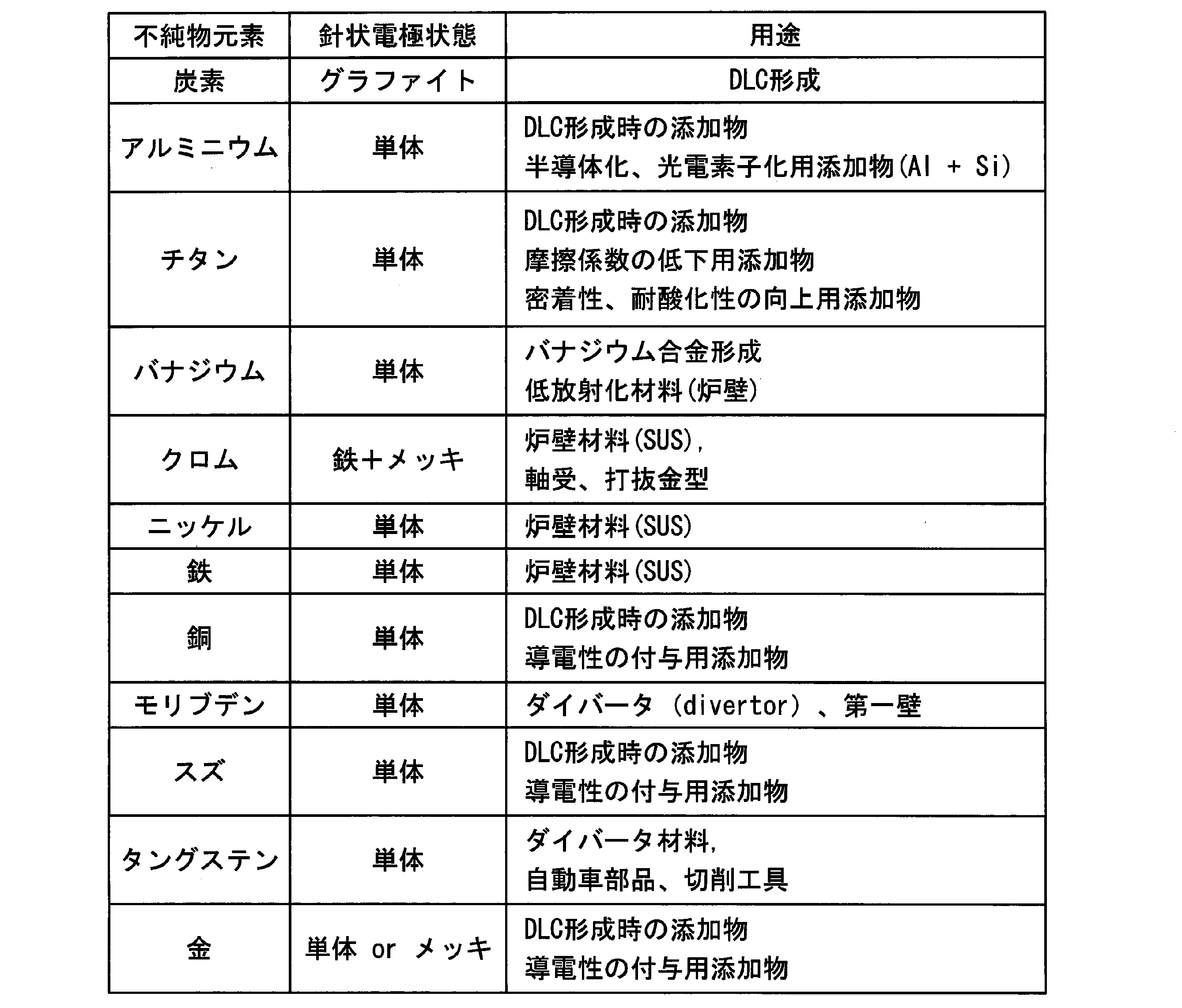
カバー電極102の他端側には、カバー電極基部104が接続される。カバー電極基部104には、針状電極101の基端が接続固定されている。カバー電極102は、一端と他端との間に円筒状の絶縁部材103を有する。ている。絶縁部材103は、外部電極11に開口するカバー電極102の一端と、カバー電極基部104と、を絶縁状態に接続する。
針状電極101は、カバー電極102、絶縁部材103、カバー電極基部104に対して、これらの軸線と一致するように中心に配置されている。
カバー電極102、絶縁部材103、カバー電極基部104は、いずれも針状電極101と離間するように、かつ、これらの内部が真空減圧可能に密閉されている。
針状電極101は、カバー電極102、絶縁部材103、カバー電極基部104に対して、これらの軸線と一致するように中心に配置されている。
カバー電極102、絶縁部材103、カバー電極基部104は、いずれも針状電極101と離間するように、かつ、これらの内部が真空減圧可能に密閉されている。
カバー電極基部104は、針状電極101の基端が接続固定された分離部分105が、カバー電極102に対して分離可能とされる。針状電極101の基端は、圧着端子を用いて分離部分105に接続されていてもよい。
具体的には、針状電極101の基端は、圧着端子や止めネジを用いた圧着などを採用して分離部分105に接続することができる。
具体的には、針状電極101の基端は、圧着端子や止めネジを用いた圧着などを採用して分離部分105に接続することができる。
不純物生成部100は、分離部分105をカバー電極基部104側から分離することで、分離部分105および針状電極101を、カバー電極102、絶縁部材103、カバー電極基部104に対して、分離することが可能となっている。なお、カバー電極基部104と分離部分105とは、互いに接続した状態では密閉可能とされる。
カバー電極102が外部電極11に開口する内径寸法は、外部電極11と内部電極12との径方向距離(間隔)とほぼ同等か、これより小さく設定される。つまり、カバー電極102における開口寸法は、外部電極11の円筒面と内部電極12の円筒面との径方向距離とほぼ同等か、これより小さく設定してもよい。
カバー電極102が外部電極11に開口する内径寸法は、外部電極11と内部電極12との径方向距離(間隔)とほぼ同等か、これより小さく設定される。つまり、カバー電極102における開口寸法は、外部電極11の円筒面と内部電極12の円筒面との径方向距離とほぼ同等か、これより小さく設定してもよい。
不純物生成部100は、図3に示すように、外部電極11および内部電極12の軸と直交する面において、外部電極11および内部電極12で形成される円環状の磁化プラズモイド生成空間に対して、外部電極11の径方向の両端位置となるように2箇所設置される。2本の不純物生成部100は、互いに平行状態、かつ、針状電極101の先端が互いに逆向きとなるように設定されている。
不純物生成部100は、外部電極11および内部電極12の軸と直交(交差)する面において、ノズル13aと直交するように複数配置される。
カバー電極102の配置とノズル13aの配置とは、軸直交面において点対称とすることができる。つまり、カバー電極102とノズル13aとは、外部電極11および内部電極12の軸に対して対称に配置することができる。
カバー電極102の配置とノズル13aの配置とは、軸直交面において点対称とすることができる。つまり、カバー電極102とノズル13aとは、外部電極11および内部電極12の軸に対して対称に配置することができる。
カバー電極102は、外部電極11を外部から貫通するように外部電極11の内部に向けて開口する。カバー電極102および針状電極101の軸線方向は、軸直交面において、円環状の磁化プラズモイド生成空間に対して、その接線方向に沿って配置される。カバー電極102は、軸直交面において、内部電極12の周囲で径方向外側に針状電極101を位置する。カバー電極102は、軸直交面において、内部電極12の接線方向に針状電極101を位置する。
針状電極101の先端の配置としては、磁化プラズモイド生成空間の外側、つまり、円筒状となる外部電極11の表面をカバー電極102の開口部分で延長した円筒面よりも内部電極12側に突出しない位置とすることができる。
さらに、針状電極101の先端の配置として、外部電極11よりも磁化プラズモイド生成空間の内部に突出した状態、あるいは、外部電極11よりも磁化プラズモイド生成空間の外側位置、つまり、カバー電極基部104側となる位置である状態とすることもできる。
不純物生成部100には不純物生成電源が接続される。
不純物生成電源は、カバー電極102とカバー電極基部104とに接続され、針状電極101のみをスパッタするため、ダイオードを用いたクローバ回路とすることができる。不純物生成電源は、その機能が電源制御部14に含有される。
不純物生成電源は、カバー電極102とカバー電極基部104とに接続され、針状電極101のみをスパッタするため、ダイオードを用いたクローバ回路とすることができる。不純物生成電源は、その機能が電源制御部14に含有される。
具体的には、クローバ回路は、図3に示すように、電源V1を有する回路と、コンデンサC02を有する回路とを並列に接続し、それらの回路は、イグナイトロンIT(スイッチ素子)を介して、バイパス用ダイオードD03の回路と負荷であるカバー電極102とカバー電極基部104とに並列に接続してある。コンデンサC02の回路は、クローバ回路であり、コンデンサC02は、クローバ用コンデンサである。コンデンサC02は、充電用コンデンサである。
図3に示すクローバ回路は一例であり、後述するバイアスコイル15のパルス駆動に対して、針状電極101から不純物を拡散可能なスパッタ電圧を印加できるものであれば、この構成に限ることはない。
図3に示すクローバ回路は一例であり、後述するバイアスコイル15のパルス駆動に対して、針状電極101から不純物を拡散可能なスパッタ電圧を印加できるものであれば、この構成に限ることはない。
電源制御部14は、プラズマ電源(電源回路)と、バイアスコイル用パルス電源と、不純物生成電源と、これらを制御する制御部と、を有する。
電源制御部14におけるプラズマ電源(電源回路)は、外部電極11と内部電極12との間に負荷信号を印加するものである。プラズマ電源(電源回路)は、例えば直流的に負荷信号を印加するものであってもよいし、連続パルス信号を印加するものであってもよい。なお、負荷信号とは、外部電極11と内部電極12間に印加した負荷電圧、またはそのとき流れた負荷電流を意味する。
図4は、本実施形態における磁化プラズモイド射出装置におけるプラズマ電源(電源回路)の一例を示す回路図である。
プラズマ電源(電源回路)は、コンデンサC1、インダクタンスL1、抵抗R1の回路と、バイパス用ダイオードD2を並列に接続したコンデンサC2、インダクタンスL2、抵抗R2、ダイオードD1の回路とを並列に接続し、それらの回路は、イグナイトロンIT(スイッチ素子)を介して負荷Fに接続してある。前記ダイオードD1、コンデンサC2等の回路は、パワークローバ回路であり、ダイオードD1は、クローバスイッチ、コンデンサC2は、パワークローバ用コンデンサである。コンデンサC1,C2は、充電用コンデンサである。
プラズマ電源(電源回路)は、コンデンサC1、インダクタンスL1、抵抗R1の回路と、バイパス用ダイオードD2を並列に接続したコンデンサC2、インダクタンスL2、抵抗R2、ダイオードD1の回路とを並列に接続し、それらの回路は、イグナイトロンIT(スイッチ素子)を介して負荷Fに接続してある。前記ダイオードD1、コンデンサC2等の回路は、パワークローバ回路であり、ダイオードD1は、クローバスイッチ、コンデンサC2は、パワークローバ用コンデンサである。コンデンサC1,C2は、充電用コンデンサである。
コンデンサC1,C2は、それらの容量がC1<C2となるように、即ちコンデンサC2は、コンデンサC1よりも容量の大きいものを用いる。コンデンサC1,C2の電圧Vc1,Vc2は、同じ極性で、Vc1>Vc2となるように、即ちコンデンサC1の電圧Vc1がコンデンサC2の電圧Vc2よりも高くなるように充電する。
この状態で制御部(図示せず)の制御によりイグナイトロンITを導通すると、コンデンサC1は、放電を開始して放電電流Ic1が流れ、負荷Fに負荷電流IL(=Ic1)が流れる。この際、ダイオードD1は、コンデンサC1の電圧Vc1に対して非導通になるから、コンデンサC2は放電しない。コンデンサC1の放電が進み、コンデンサC1の電圧Vc1がコンデンサC2の電圧Vc2よりも低くなると、ダイオードD1が導通してコンデンサC2が放電を開始し、コンデンサC2の放電電流Ic2が負荷Fに流れる。
以後、負荷Fには、放電電流Ic1,Ic2(IL=Ic1+Ic2)が流れる。負荷電流ILは、ダイオードD2を流れて還流する。したがって負荷電流ILは、非振動の単極減衰電流となる。
以後、負荷Fには、放電電流Ic1,Ic2(IL=Ic1+Ic2)が流れる。負荷電流ILは、ダイオードD2を流れて還流する。したがって負荷電流ILは、非振動の単極減衰電流となる。
コンデンサC1のみの場合には、負荷電流は、短時間で減衰してしまうが、容量の大きいコンデンサC2の放電が加わることにより、負荷電流ILは緩やかに減衰する。そして負荷電流ILの立ち上がりは、コンデンサC1によって決まるから急峻になる。即ち、図4に示すパワークローバ回路は、立ち上りが急峻で減衰の緩やかな負荷電流を供給することができ、1回の充電で連続的にプラズマ塊を生成することができる。
図4に示すパワークローバ回路は、容量が小さいコンデンサC1と容量が大きいパワークローバ用のコンデンサC2を用い、コンデンサC1の充電電圧をコンデンサC2の充電電圧よりも高くする。これにより、負荷電流の立ち上り時は、コンデンサC1の放電電流が寄与し、その後は主としてコンデンサC2の放電電流が寄与するから、負荷電流は、立ち上りが急峻になり、減衰は緩やかになる。またクローバスイッチには、ダイオードD1を用い、コンデンサC1の放電電圧がコンデンサC2の充電電圧よりも低くなると、ダイオードD1が自動的に導通してコンデンサC2の放電を開始する。
イグナイトロンITは、イグナイトロンに代えて制御部の制御により導通、非導通の切換えが可能な他の半導体スイッチを用いることもできる。またイグナイトロンITは、抵抗R1と直列に、ダイオードD1の接続点よりも抵抗R1側に接続してもよい。また抵抗R1,R2は、小さいほどロスが小さくなり、インダクタンスL1,L2は、小さいほど負荷電流ILの脈動が小さくなる。そしてインダクタンスL1をインダクタンスL2よりも大きくすると、負荷電流ILのコンデンサC1への戻りが小さくなり、負荷電流ILの大部分は、前記パワークローバ回路を経由して流れる。
電源制御部14におけるバイアスコイル用パルス電源は、バイアスコイル15をパルス駆動するものである。バイアスコイル用パルス電源は、例えば所定の周波数のサイン波電流をバイアスコイル15に印加可能に構成されている。また、例えばトランジスタを用いて電源(コンデンサ)をインバータ制御して、矩形波の連続パルス信号をバイアスコイル15に印加するようにしてもよい。
また、電源制御部14における制御部は、バイアスコイル15をパルス駆動するようにバイアスコイル用パルス電源を制御するとともに、プラズマ電源(電源回路)から外部電極11と内部電極12との間に出力する付加信号を制御するとともに、不純物生成電源を制御するものである。
バイアスコイル15は、内部電極12の内部に配置される。これにより、超高真空を得るために必須である真空容器のベーキングが、バイアスコイルの影響を受けることなく可能となる。このため、吸着ガスの除去が可能となる。バイアスコイル15は、外部電極11と内部電極12間に発生したプラズマに対して、バイアス磁場を印加するものである。これにより、プラズマが放電電流による磁場とバイアス磁場を含んだ状態で放出されるので、スフェロマックプラズマが生成されることになる。
電源制御部14における制御部は、スフェロマックプラズマが生成されるのに必要なバイアス磁場が外部電極11と内部電極12との間に与えられるのに十分な時間、かつ、磁束保持部へのバイアス磁場の磁束の染み込み時間よりも短い時間でバイアスコイル15をパルス駆動するように、バイアスコイル用パルス電源を制御する。即ち、磁束保持部に磁束が染み込まないような時間間隔でバイアス磁場の磁束の空間分布を制御し、外部電極11と内部電極12の間に効率よく、必要なバイアス磁場を発生させるように制御する。
磁束保持部は、バイアスコイル15により印加されるバイアス磁場の磁束を外部に漏らさないようにするために用いられる。
例えば、図1に示す例では、磁束保持部は外部電極11と一体として形成されている。即ち、外部電極11を銅等、高導電率かつ低透磁率の材料で構成するとともに、その外部電極11の厚みを、バイアス磁場に必要な時間よりも長く、かつ磁束が磁束保持部に染み込む時間よりも短い時間となるのに足りる厚みとなるように設計する。
例えば、図1に示す例では、磁束保持部は外部電極11と一体として形成されている。即ち、外部電極11を銅等、高導電率かつ低透磁率の材料で構成するとともに、その外部電極11の厚みを、バイアス磁場に必要な時間よりも長く、かつ磁束が磁束保持部に染み込む時間よりも短い時間となるのに足りる厚みとなるように設計する。
あるいは、磁束保持部は、外部電極11に対して着脱可能に構成されてもよい。これにより、プラズマ生成条件等に応じて磁束保持部の厚みを変えることも可能である。
この場合、磁束保持部は、外部電極11の外形状に合わせ形成される。例えば外部電極11が円筒形状であれば、それに合わせて磁束保持部も円筒形状となる。そして、磁束保持部は、ジャケット状、またはシェル状に、おおむね外部電極11を覆うように構成される。
この場合、磁束保持部は、外部電極11の外形状に合わせ形成される。例えば外部電極11が円筒形状であれば、それに合わせて磁束保持部も円筒形状となる。そして、磁束保持部は、ジャケット状、またはシェル状に、おおむね外部電極11を覆うように構成される。
同時に、着脱可能な磁束保持部は、外部電極11の外側に配置される。磁束保持部は、高導電率かつ低透磁率の材料からなるものである。例えば、銅や銅合金等であればよい。磁束保持部の長さについては、バイアスコイル15の長さと同等以上の長さを有していれば、バイアスコイル15から発生するバイアス磁場の磁束を効率よく閉じ込めることが可能となる。
磁束保持部の厚みについては、スフェロマックプラズマが生成されるのに必要なバイアス磁場が外部電極11と内部電極12との間に与えられるのに十分な時間だけバイアスコイル15を駆動しても、磁束保持部に磁束が染み込んで通り抜けないような厚みを有する。磁束保持部に磁束が長い時間加わると、磁束保持部に染み込んで通り抜けてしまうため、バイアス磁場に必要な時間よりも長く、かつ磁束が染み込む時間と磁束保持部の厚みとを考慮して、パルス駆動時間を設定する。
電源制御部14における制御部は、不純物生成電源を制御して、不純物生成部100の針状電極101に電圧を印加し、磁化プラズモイド生成空間に不純物を拡散するとともに、バイアスコイル用パルス電源を制御して、スフェロマックプラズマが生成されるのに必要なバイアス磁場を外部電極11と内部電極12との間に印加した状態で、プラズマ電源(電源回路)を制御して、外部電極11と内部電極12との間に放電電圧を印加する。
このとき、電源制御部14における制御部が、針状電極101に電圧を印加すると同時もしくはその前後に、バイアス磁場を印加し、その後に外部電極11と内部電極12との間に放電電圧を印加することで、生成されるプラズマ中に不純物が含有される。
この際、例えば、針状電極101に電圧を印加した後、数マイクロ秒から、数100マイクロ秒後に、バイアス磁場を形成し、プラズマ生成用に放電させる制御をおこなうことが好ましい。
あるいは、各パルス放電および不純物元素の拡散の時間スケールに応じて針状電極101への電圧印加やバイアス磁場の印加のタイミングを設定することで、生成されるプラズマ中に不純物を含有させる。
この際、例えば、針状電極101に電圧を印加した後、数マイクロ秒から、数100マイクロ秒後に、バイアス磁場を形成し、プラズマ生成用に放電させる制御をおこなうことが好ましい。
あるいは、各パルス放電および不純物元素の拡散の時間スケールに応じて針状電極101への電圧印加やバイアス磁場の印加のタイミングを設定することで、生成されるプラズマ中に不純物を含有させる。
次に、本実施形態における磁化プラズモイド射出装置10における不純物を含有する磁化プラズモイド生成について説明する。
図5は、本実施形態における磁化プラズモイド射出装置における不純物拡散状態を示す横断面図であり、図6は、本実施形態における磁化プラズモイド射出装置におけるプラズマ生成状態を示す縦断面図であり、図7は、本実施形態における磁化プラズモイド射出装置におけるプラズマ生成状態を示す横断面図である。
本実施形態における磁化プラズモイド射出装置10では、まず、プラズマ生成ガス供給部13からプラズマ生成ガスを供給する。
本実施形態における磁化プラズモイド射出装置10では、まず、プラズマ生成ガス供給部13からプラズマ生成ガスを供給する。
プラズマ生成ガスは、ノズル13aから円環状となる外部電極11と内部電極12との間の磁化プラズモイド生成空間の接線方向に噴出される。これにより磁化プラズモイド生成空間におけるプラズマ生成ガスの流れを安定させ、また、導入されたガス密度を空間的に一様にする。
次いで、電源制御部14における制御部は、不純物生成電源を制御して、不純物生成部100の針状電極101に電圧を印加し、図5に示すように、磁化プラズモイド生成空間に不純物を拡散する。
この際、不純物が磁化プラズモイド生成空間において拡散する範囲は、例えば、外部電極11と内部電極12との軸方向において、ノズル13aを中心とした領域でプラズマの生成される範囲よりと同等かそれより小さくなるように設定されることが好ましい。不純物の拡散範囲の制御は、例えば、ガス導入時刻と、不純物生成部100での放電、および、磁化プラズモイド生成部の放電のタイミングなどとを設定することによっておこなうことができる。磁化プラズモイド生成部の放電は、バイアスコイル用パルス電源、プラズマ電源(電源回路)によりタイミングを設定する。
次いで、電源制御部14における制御部は、図6に示すように、バイアスコイル用パルス電源を制御して、スフェロマックプラズマが生成されるのに必要なバイアス磁場を外部電極11と内部電極12との間に印加した状態で、プラズマ電源(電源回路)を制御して、外部電極11と内部電極12との間に放電電圧を印加する。
具体的には、外部電極11と内部電極12との間の空間に電源制御部14におけるプラズマ電源(電源回路)により負荷信号を印加すると、外部電極11と内部電極12との間に放電が発生し、図7に示すように、放電電流が流れてプラズマPが生成される。そして、バイアスコイル15によるバイアス磁場が、バイアスコイル用パルス電源、磁束保持部、制御部により空間分布制御され、磁束がプラズマ生成領域に分散する。
生成されたプラズマPは、放電電流による磁場とともに、バイアスコイル15によるバイアス磁場により、ポロイダル方向とトロイダル方向の磁場が生じ、スフェロマックプラズマとして外部電極11と内部電極12の開放端から放出される。放出されたスフェロマックプラズマは、すぐには拡散することなく、プラズマ塊の状態のまま高速で放出される。
このとき、プラズマが生成される前に、磁化プラズモイド生成空間においては、不純物が拡散されているため、生成されたプラズマPには、拡散された不純物を所定の濃度及び濃度分布で含有させることができる。
このように、生成されたプラズマPに拡散された不純物を含有するためには、例えば、針状電極101がガス導入箇所となるノズル13aの近傍に設置され、またバイアス磁場形成と同時に不純物を拡散することで、イオン化された不純物元素をプラズマP内に捕捉できるように設定されることが好ましい。
このように、生成されたプラズマPに拡散された不純物を含有するためには、例えば、針状電極101がガス導入箇所となるノズル13aの近傍に設置され、またバイアス磁場形成と同時に不純物を拡散することで、イオン化された不純物元素をプラズマP内に捕捉できるように設定されることが好ましい。
本実施形態における磁化プラズモイド射出装置10においては、磁化プラズモイド生成空間の接線方向にノズル13aからプラズマ生成ガスを供給する。これにより、磁化プラズモイド射出装置10は、ニュートラルな状態として、安定したプラズマを発生させることが可能となる。
また、本実施形態における磁化プラズモイド射出装置10では、ノズル13aと同一平面として磁化プラズモイド生成空間の接線方向に不純物生成部100を設けた。これにより、従来の装置においてはイオン化した不純物をバイアス磁界により弾かれてしまうためプラズマに含有させることが難しかったのに対して、本実施形態の磁化プラズモイド射出装置10は、イオン化した不純物を容易にプラズマに含有させることが可能となる。同時に、本実施形態の磁化プラズモイド射出装置10は、生成したプラズマの安定度を向上することができる。
さらに、本実施形態の磁化プラズモイド射出装置10は、針状電極101をスパッタすることで不純物を磁化プラズモイド生成空間に供給する。このため、本実施形態の磁化プラズモイド射出装置10は、スパッタにより発生する不純物の量を精密に制御することが容易となる。したがって、本実施形態の磁化プラズモイド射出装置10は、磁化プラズモイドに含有させる不純物濃度を極めて正確に設定することが可能となる。
同時に、本実施形態の磁化プラズモイド射出装置10は、針状電極101を交換する、あるいは、予め所定の針状電極101を取り付けることで、不純物を所望の種類とすることができる。これにより、本実施形態の磁化プラズモイド射出装置10は、プラズマに含有させる不純物の量および組成比を、極めて短い時間、すなわち、パルス状に発生する磁化プラズモイド単位ごとに、制御することが可能となる。これによって、本実施形態の磁化プラズモイド生成装置10は、発射するプラズマにおいて、含有される不純物量および組成比の時間的変化を容易に設定することが可能となる。
さらに、本実施形態の磁化プラズモイド射出装置10は、不純物生成部100から不純物を供給し、生成された磁化プラズモイドが外部電極11と内部電極12とで形成された磁化プラズモイド生成空間を進行して発射される間に、不純物を磁化プラズモイドに均一化して含有させる。これにより、本実施形態の磁化プラズモイド射出装置10は、磁化プラズモイド生成空間の軸方向長さに応じて、不純物濃度が均一化した磁化プラズモイドを生成・射出することができる。
また、本実施形態の磁化プラズモイド射出装置10は、針状電極101をスパッタしない状態と、針状電極101をスパッタする状態とを切り替えることができる。これにより本実施形態の磁化プラズモイド射出装置10は、不純物を含まないプラズマと不純物を含むプラズマとを切り替えて、それぞれ所定の時間だけ生成することも可能となる。
本実施形態の磁化プラズモイド射出装置10は、不純物生成部100が磁化プラズモイド生成空間の接線方向に設けられていることにより、内部電極12表面に針状電極101から発生した不純物が付着することを極めて低減することが可能となる。
同時に、本実施形態の磁化プラズモイド射出装置10は、ノズル13aから供給されたプラズマ生成ガスにより、内部電極12表面に付着物等の不具合が発生することを低減可能である。
同時に、本実施形態の磁化プラズモイド射出装置10は、ノズル13aから供給されたプラズマ生成ガスにより、内部電極12表面に付着物等の不具合が発生することを低減可能である。
また、本実施形態の磁化プラズモイド射出装置10は、不純物生成部100における針状電極101の交換のみで、不純物の種類を変更することができるため、磁化プラズモイド生成空間の全域を開放して交換する必要がなく、装置内部に対する外部からの汚染等悪影響を低減することができる。
これらにより、本実施形態の磁化プラズモイド射出装置10は、装置のメンテナンスにおける作業工程を削減し、メンテナンス時間を低減することが可能となる。
これらにより、本実施形態の磁化プラズモイド射出装置10は、装置のメンテナンスにおける作業工程を削減し、メンテナンス時間を低減することが可能となる。
さらに、本実施形態における磁化プラズモイド射出装置10においては、不純物生成部100から不純物を磁化プラズモイド生成空間に生成した直後に、バイアス磁場を形成するとともに外部電極11と内部電極12との間にプラズマ放電をおこなうことで、従来は、バイアス磁場に弾かれてしまったイオン化された不純物をプラズマ中に含有することが可能となる。
なお、本実施形態では、プラズマ生成ガス供給部13のノズル13aが外部電極11の径方向外側に設けられる例を示したが、本発明はこれに限定されない。外部電極11と内部電極12の間にプラズマ生成ガスが供給可能であれば、例えば内部電極12の径方向内側にプラズマ生成ガス供給部が設けられてもよい。
なお、本実施形態の磁化プラズモイド射出装置10では、プラズマ生成ガス供給部13のノズル13aと不純物生成部100とを、それぞれ異なる位置として外部電極11に開口させたが、これに対して、不純物生成部100の基部側からプラズマ生成ガスを供給することで、不純物生成部100とノズルとを兼用させることもできる。この場合、磁化プラズモイド生成空間に供給する不純物量を増大させて、不純物濃度を増加した磁化プラズモイドを生成することが可能となる。
また、本実施形態の磁化プラズモイド射出装置10は、バイアスコイル15の中央付近にプラズマ生成ガスを供給したが、この場合に、磁化プラズモイドに含まれる磁束を増やすための効率が最もよくなる。これは、本実施形態のようにプラズマ生成ガス供給部13のノズル13aが、外部電極11の外側を覆う磁束保持部の一部を貫通するように設けられることで可能になる。
さらに、本実施形態の磁化プラズモイド射出装置10では、プラズマ生成ガス供給部13のノズル13aと不純物生成部100とをそれぞれ、2本ずつ外部電極11に開口させたが、本発明はこれに限定されない。3本以上の複数本を設けることもできる。この場合、ノズル13aと不純物生成部100とが円筒状の磁化プラズモイド生成空間の接線方向に設けられることができる。
また、本実施形態の磁化プラズモイド射出装置10では、複数のプラズマ生成ガス供給部13のノズル13aと不純物生成部100とが磁化プラズモイド生成空間の軸と交差する同一面内に配置されたが、これらを磁化プラズモイド生成空間の軸方向の位置が異なる平行面内にそれぞれ位置するように配置することもできる。あるいは、複数のプラズマ生成ガス供給部13のノズル13aと不純物生成部100とが軸直交面に沿った方向とは異なる方向に配置されてもよい。この場合でも、不純物生成部100とノズル13aとは、円筒状の磁化プラズモイド生成空間の接線方向に設けられることができる。
さらに、それぞれ複数本設けられる不純物生成部100とノズル13aとのうち、いずれか一本、または、適宜選択された複数本が、外部電極11および内部電極12の軸と直交する面以外の方向に沿った状態として、傾斜して交差する面内に配置されることができる。この場合でも、不純物生成部100とノズル13aとは、円筒状の磁化プラズモイド生成空間の接線方向に設けられることができる。
なお、不純物生成部100を設けないこともできる。
なお、不純物生成部100を設けないこともできる。
以下、本発明に係る磁気閉じ込めプラズマ装置の第2実施形態を、図面に基づいて説明する。
図8は、本実施形態における磁気閉じ込めプラズマ装置を示す模式図である。本実施形態において、上述した第1実施形態と異なるのは、磁化プラズモイドを射出する部分に関する点であり、これ以外の上述した第1実施形態と対応する構成には同一の符号を付してその説明を省略する。
図8は、本実施形態における磁気閉じ込めプラズマ装置を示す模式図である。本実施形態において、上述した第1実施形態と異なるのは、磁化プラズモイドを射出する部分に関する点であり、これ以外の上述した第1実施形態と対応する構成には同一の符号を付してその説明を省略する。
本実施形態における磁気閉じ込めプラズマ装置20は、図8に示すように、磁化プラズモイド射出装置10と、磁化プラズモイド射出装置10がプラズマを射出する部分として磁気閉じ込めプラズマ部21を有する。
磁気閉じ込めプラズマ部21は、例えば、核融合炉の炉心とされ、磁化プラズモイド射出装置10によって、トレーサーとなる元素を含む磁化プラズモイドが入射される。
磁気閉じ込めプラズマ部21は、例えば、射出された元素を含む磁化プラズモイドにより、炉内におけるプラズマの挙動を分光器等によって分析可能なものとされる。
磁気閉じ込めプラズマ部21は、プラズモイド入射に必要なポート、閉じ込め磁界を形成するコイル、その他対象となるプラズマの生成に必要な電源、真空ポンプなどから構成される。
本実施形態における磁化プラズモイド射出装置10において、一箇所の針状電極101は導電性の材料で構成されればよく、化合物や合金を用いてもよい。例えば、針状電極101は、W,Sn,Nd,Sm,Gd,Tb,Dy,Er,Yb,Au,Pb,Bi,Ti,Cu,C,Al,Moから選択される1以上の元素からなるものとすることができる。また、これらの針状電極101を有する不純物生成部100を複数設けることができる。
磁気閉じ込めプラズマ部21は、例えば、射出された元素を含む磁化プラズモイドにより、炉内におけるプラズマの挙動を分光器等によって分析可能なものとされる。
磁気閉じ込めプラズマ部21は、プラズモイド入射に必要なポート、閉じ込め磁界を形成するコイル、その他対象となるプラズマの生成に必要な電源、真空ポンプなどから構成される。
本実施形態における磁化プラズモイド射出装置10において、一箇所の針状電極101は導電性の材料で構成されればよく、化合物や合金を用いてもよい。例えば、針状電極101は、W,Sn,Nd,Sm,Gd,Tb,Dy,Er,Yb,Au,Pb,Bi,Ti,Cu,C,Al,Moから選択される1以上の元素からなるものとすることができる。また、これらの針状電極101を有する不純物生成部100を複数設けることができる。
本実施形態の磁気閉じ込めプラズマ装置20によれば、従来は含有することの難しかった不純物を炉内である磁気閉じ込めプラズマ部21に供給して、分光器等によってその挙動を観察・測定することが可能となる。
ここで、従来の磁気閉じ込めプラズマ装置では、パフと呼ばれる微小な固体状のトレーサー元素、あるいは、不純物を含有したペレットをイオン化あるいは蒸発させて、磁気閉じ込めプラズマ部21に供給していた。これに対して、本実施形態の磁気閉じ込めプラズマ装置20は、トレーサーとなる元素を含む磁化プラズモイドを供給可能とすることで、固体を供給することで生じていた磁気閉じ込めプラズマ部21におけるプラズマエネルギーの減少(プラズマの局所的な冷却)を防止しつつ、トレーサー元素を供給することが可能となる。これにより、磁気閉じ込めプラズマ部21におけるプラズマの挙動に与える変化を最小にして、かつ、トレーサー元素を供給することが可能となる。
また、本実施形態によれば、従来は難しかった、トレーサーとなる元素を含む磁化プラズモイドを供給できるため、あらかじめイオン化した不純物を容易に磁気閉じ込めプラズマ部21のプラズマに供給することが可能となる。同時に、生成したプラズマの安定度を向上することができる。
また、従来の固体ペレットを使った手法では、入射速度が遅いためコアプラズマへ到達する前に電離してしまうため、閉じ込め磁場に遮られてトレーサーを中心部へ運搬できないといった不具合を生じていたが、本実施形態の磁気閉じ込めプラズマ装置20は、この不具合を生じることなく、トレーサーとなる元素を含む磁化プラズモイドを供給できる。
また、従来の固体ペレットを使った手法では、入射速度が遅いためコアプラズマへ到達する前に電離してしまうため、閉じ込め磁場に遮られてトレーサーを中心部へ運搬できないといった不具合を生じていたが、本実施形態の磁気閉じ込めプラズマ装置20は、この不具合を生じることなく、トレーサーとなる元素を含む磁化プラズモイドを供給できる。
さらに、本実施形態の磁気閉じ込めプラズマ装置20は、不純物生成部100を備えているため、射出する磁化プラズモイドが含むトレーサーとなる元素の量を精密に制御することが容易となる。これにより、本実施形態の磁気閉じ込めプラズマ装置20は、磁気閉じ込めプラズマ部21のプラズマに供給するトレーサーとなる元素の量を極めて正確に設定することが可能となる。
同時に、本実施形態の磁気閉じ込めプラズマ装置20は、不純物生成部100の針状電極101を交換する、あるいは、予め所定の針状電極101を取り付けることで、磁気閉じ込めプラズマ部21のプラズマに供給するトレーサーとなる元素を所望の種類とする、あるいは、複数種類のトレーサー元素を同時に供給することができる。これにより、本実施形態の磁気閉じ込めプラズマ装置20は、磁気閉じ込めプラズマ部21のプラズマに供給するトレーサーとなる元素の量および組成比を、極めて短い時間、すなわち、パルス状に発生して射出する磁化プラズモイド単位ごとに制御することが可能となる。これによって、本実施形態の磁気閉じ込めプラズマ装置20は、磁気閉じ込めプラズマ部21のプラズマに供給するトレーサーとなる元素量および組成比の時間的変化をも設定することが可能となる。
さらに、本実施形態の磁気閉じ込めプラズマ装置20は、磁化プラズモイド射出装置10によって、あらかじめ均一化されたトレーサーとなる元素を含有する磁化プラズモイドを磁気閉じ込めプラズマ部21のプラズマに供給することができる。これにより、本実施形態の磁気閉じ込めプラズマ装置20は、磁気閉じ込めプラズマ部21におけるトレーサー元素の均一化を向上することができる。
また、本実施形態の磁気閉じ込めプラズマ装置20は、不純物生成部100の針状電極101をスパッタしない状態と、針状電極101をスパッタする状態とを切り替えて、トレーサー元素の有無を選択して磁化プラズモイドを磁気閉じ込めプラズマ部21のプラズマに供給することも可能となる。
本実施形態の磁気閉じ込めプラズマ装置20は、不純物生成部100が磁化プラズモイド生成空間の接線方向に設けられていることにより、内部電極12表面に針状電極101から発生した不純物が付着することを極めて低減することが可能となる。
同時に、本実施形態の磁気閉じ込めプラズマ装置20は、ノズル13aから供給されたプラズマ生成ガスにより内部電極12表面に付着物等の不具合が発生することを低減可能である。
また、本実施形態の磁気閉じ込めプラズマ装置20は、不純物生成部100における針状電極101の交換のみで、トレーサー元素の種類を変更することができる。このため、本実施形態の磁気閉じ込めプラズマ装置20は、磁化プラズモイド射出装置10の磁化プラズモイド生成空間およびこれに連通する磁気閉じ込めプラズマ部21の全域を開放して交換する必要がなく、装置内部に対する外部からの汚染等悪影響を低減することができる。
これらにより、本実施形態の磁気閉じ込めプラズマ装置20は、装置のメンテナンスにおける作業工程を削減し、メンテナンス時間を低減することが可能となる。
同時に、本実施形態の磁気閉じ込めプラズマ装置20は、ノズル13aから供給されたプラズマ生成ガスにより内部電極12表面に付着物等の不具合が発生することを低減可能である。
また、本実施形態の磁気閉じ込めプラズマ装置20は、不純物生成部100における針状電極101の交換のみで、トレーサー元素の種類を変更することができる。このため、本実施形態の磁気閉じ込めプラズマ装置20は、磁化プラズモイド射出装置10の磁化プラズモイド生成空間およびこれに連通する磁気閉じ込めプラズマ部21の全域を開放して交換する必要がなく、装置内部に対する外部からの汚染等悪影響を低減することができる。
これらにより、本実施形態の磁気閉じ込めプラズマ装置20は、装置のメンテナンスにおける作業工程を削減し、メンテナンス時間を低減することが可能となる。
なお、本実施形態の磁気閉じ込めプラズマ装置20では、磁化プラズモイド射出装置10におけるプラズマ生成ガス供給部13のノズル13aと不純物生成部100とをそれぞれ、外部電極11に開口させたが、不純物生成部100の基部側からプラズマ生成ガスを供給させて、ノズルと兼用させることもできる。この場合、本実施形態の磁気閉じ込めプラズマ装置20は、磁気閉じ込めプラズマ部21に供給する磁化プラズモイドが含有するトレーサー元素量を増大させることが可能となる。
これにより、本実施形態の磁気閉じ込めプラズマ装置20は、タングステン等とされるトレーサー元素を混入させる場合に、トレーサー導入電極部となる不純物生成部100からもガス供給をおこない、針状電極101を負高圧で放電することでイオンボンビングによりスパッタ効率を上げて、トレーサー元素量を増加することができる。
これにより、本実施形態の磁気閉じ込めプラズマ装置20は、タングステン等とされるトレーサー元素を混入させる場合に、トレーサー導入電極部となる不純物生成部100からもガス供給をおこない、針状電極101を負高圧で放電することでイオンボンビングによりスパッタ効率を上げて、トレーサー元素量を増加することができる。
以下、本発明に係るプラズマ処理装置の第3実施形態を、図面に基づいて説明する。
図9は、本実施形態におけるプラズマ処理装置を示す模式図である。
本実施形態において上述した第1および第2実施形態と異なるのは射出した磁化プラズモイドによって成膜をおこなう部分に関する点であり、これ以外の対応する構成要素に関しては、同一の符号を付してその説明を省略する。
図9は、本実施形態におけるプラズマ処理装置を示す模式図である。
本実施形態において上述した第1および第2実施形態と異なるのは射出した磁化プラズモイドによって成膜をおこなう部分に関する点であり、これ以外の対応する構成要素に関しては、同一の符号を付してその説明を省略する。
本実施形態のプラズマ処理装置30は、磁化プラズモイド射出装置10から射出されるプラズマを用いて被処理基板Wにプラズマ処理、例えば、成膜処理をおこなうものとされる。
本実施形態のプラズマ処理装置30は、図9に示すように、成膜材料からなる内部電極32と、外部電極11の外側に位置するバイアスコイル35と、磁化プラズモイド射出装置10に接続されて磁化プラズモイドが射出される処理室31と、処理室31に配置されて被処理基板を保持するステージ(被処理基板保持部)39と、を有する。
本実施形態のプラズマ処理装置30は、図9に示すように、成膜材料からなる内部電極32と、外部電極11の外側に位置するバイアスコイル35と、磁化プラズモイド射出装置10に接続されて磁化プラズモイドが射出される処理室31と、処理室31に配置されて被処理基板を保持するステージ(被処理基板保持部)39と、を有する。
内部電極32は、上述した実施形態における内部電極12に対応し、成膜材料からなる円柱状に形成される。内部電極32とされる成膜材料としては、金属、カーボンまたはそれらを含む導電性の化合物または混合物を挙げることができる。
成膜対象である被処理基板Wとしては、例えばシリコン基板やアルミニウム基板、PET(ポリエチレンテレフタラート)等、種々のものが含まれる。本実施形態のプラズマ処理装置30では、放電電流によるローレンツ力によって炭素イオンを加速し被処理基板Wに入射させるため、被処理基板Wの電位制御は必ずしも必要がない。したがって、電位制御の困難な誘電体材料等にも成膜可能である。
また、本実施形態のプラズマ処理装置30は、被処理基板Wに対する電位制御が不要であるため、例えばライン生産において個々に被処理基板Wに電位印加が困難な場合にも有利である。また、本実施形態のプラズマ処理装置30は、放出されるスフェロマックプラズマは低熱負荷であるため、被処理基板Wが熱に弱いものであってもDLC(Diamond-Like Carbon)薄膜等を成膜可能である。さらに、生成されるDLC薄膜は、衝突エネルギを上げることでより硬度が高くなる。このため、本実施形態のプラズマ処理装置30は、電位印加が可能であれば積極的に被処理基板Wに電位を印加し、衝突エネルギを大きくして硬度を高めることも可能である。
また、本実施形態のプラズマ処理装置30は、被処理基板Wに対する電位制御が不要であるため、例えばライン生産において個々に被処理基板Wに電位印加が困難な場合にも有利である。また、本実施形態のプラズマ処理装置30は、放出されるスフェロマックプラズマは低熱負荷であるため、被処理基板Wが熱に弱いものであってもDLC(Diamond-Like Carbon)薄膜等を成膜可能である。さらに、生成されるDLC薄膜は、衝突エネルギを上げることでより硬度が高くなる。このため、本実施形態のプラズマ処理装置30は、電位印加が可能であれば積極的に被処理基板Wに電位を印加し、衝突エネルギを大きくして硬度を高めることも可能である。
処理室31は、所定の成膜条件を満たして密閉される。処理室31の構造は、内部でプラズマ処理が可能であれば、特に限定はされない。処理室31は真空チャンバとされる。処理室31は、磁化プラズモイド射出装置10に接続される。処理室31は、外部電極11と内部電極32の開放端から放出されたプラズマを受ける構成である。具体的には、処理室31は、絶縁体を介して外部電極11の開放端に接続されており、放出されたプラズマが内部に導入される。
バイアスコイル35は、外部電極11の外周を囲むように巻回されることができる。バイアスコイル35は、外部電極11と内部電極32との間に、絶縁破壊を促進するために実効的な電極間距離を伸ばすための垂直磁界を与える。同時に、バイアスコイル35は、外部電極11と内部電極32の間に発生したプラズマに対してバイアス磁場を印加する。これらのバイアスコイル35の機能により、プラズマが放電電流による磁場とバイアス磁場を含んだ状態で放出される。したがって、バイアスコイル35の機能により、スフェロマック様の磁場構造を持った、孤立した磁化プラズモイドが生成され、磁界によりフィルタされる。
ステージ39は、処理室31内に固定される。ステージ39は、内部電極32の軸方向に対して垂直に被処理基板Wの成膜する被処理面を対向させるように保持する。ステージ39は、磁化プラズモイド射出装置10から被処理基板Wまでの間の距離を連続的に変化可能なように構成されていてもよい。また、ステージ39は、プラズマイオンをステージ39側に引き込むように、接地または負電圧とされてもよい。この場合、処理室31とステージ39は絶縁されればよい。
ステージ39は、磁化プラズモイド射出装置10の中心と被処理基板Wの中心とが一致するように配置されることができる。
ステージ39は、磁化プラズモイド射出装置10の中心と被処理基板Wの中心とが一致するように配置されることができる。
本実施形態のプラズマ処理装置30における成膜時には、まず、磁化プラズモイド射出装置10において、プラズマ生成ガス供給部13からプラズマ生成ガスである、例えばアルゴンガスを磁化プラズモイド生成空間に供給する。プラズマ処理装置30における成膜時には、また、不純物生成部100によって磁化プラズモイド生成空間に不純物を供給する。
また、プラズマ処理装置30における成膜時には、バイアスコイル35により外部電極11と内部電極32との間に垂直磁界を与える。これにより磁化プラズモイド生成空間で、電子が内部電極32の外周を回りながら外部電極11に到達することになる。したがって、実効的な電極間距離が伸びて絶縁破壊が促進され、プラズマが放電される。そして、外部電極11と内部電極32との間に放電電圧を印加することで、外部電極11と内部電極32との間で放電させてプラズマを生成する。この放電に伴い、プラズマ中には径方向の電流が流れる。また、プラズマには、内部電極32の電流によりトロイダル磁場が生ずる。この放電の際に、成膜材料からなる内部電極32の表面が削り取られ、プラズマに混入する。
そして、プラズマ処理装置30における成膜時には、プラズマ中の径方向の電流とトロイダル方向の磁場によるローレンツ力により、バイアス磁場を引きずりながら内部電極32の軸方向に加速される。さらに、プラズマ処理装置30における成膜時には、磁気再結合により、磁化プラズモイド射出装置10の先端側でのバイアス磁場がポロイダル磁場となり、スフェロマックプラズマが外部電極11と内部電極32の開放端から放出される。
スフェロマックプラズマは、すぐには拡散することなく、プラズマ塊の状態のまま高速で放出される。スフェロマックプラズマには、内部電極32の表面が削り取られた成膜材料の粒子(イオン)が含まれているため、スフェロマックプラズマを被処理基板Wに衝突させることで、被処理基板W上に成膜材料粒子が堆積する。
なお、内部電極32から溶発したマクロ粒子は、電荷をもたないため電磁加速を受けず、そのままでは成膜には寄与しない。このプラズマ放電を複数回繰り返し行うことで、プラズマ処理装置30は、所望の膜厚になるまで被処理基板W上に不純物の含有した成膜材料粒子を堆積させていき、所望の被処理膜を得ることが可能となる。
本実施形態のプラズマ処理装置30は、被処理基板Wへの成膜時に、形成される膜の膜厚方向に不純物濃度を所定の状態に制御することが可能である。特に、プラズマ処理装置30は、不純物生成部100によって、生成される磁化プラズモイドに含有される不純物濃度を所定の状態に制御することで、被処理基板Wへ成膜される被処理膜において、膜厚方向に不純物濃度を変化させるができる。あるいは、プラズマ処理装置30は、2箇所の不純物生成部100の針状電極101をそれぞれ異なる種類からなるものとして、2箇所の不純物生成部100からの不純物供給量を個別に制御することで、膜厚方向に異なる濃度傾斜を有する被処理膜を成膜することができる。
さらに、プラズマ処理装置30は、成膜処理時間中に、2箇所の不純物生成部100からの不純物供給をおこなわない状態とすることで、膜厚方向の処置の場所で、不純物を含まない領域を形成することもできる。また、プラズマ処理装置30は、針状電極101を形成する不純物を適切に選択することで、従来はできなかった種類の不純物を含む成膜をおこなうことも可能である。
特に、グロー放電によるプラズマを用いるプラズマ成膜においては、スパッタリングターゲットを所定の組成比として製造することが極めて難しい場合でも、ターゲット製造の困難性とは関係なく、プラズマ処理装置30は、所定組成の成膜をおこなうことが可能となる。さらに、ターゲットを用いる成膜では、膜厚方向に傾斜した組成比を形成することが難しい場合でも、プラズマ処理装置30は、これを容易に実現することが可能となる。
また、プラズマ処理装置30は、ターゲットのエロージョン領域で発生する不具合、特にターゲットのひび割れ、あるいは、ターゲット合金中における組成比の不均一性や、イオン化・プラズマ化の不均一性などに影響されずに所定組成の成膜をおこなうことが可能となる。
本実施形態のプラズマ処理装置30は、成膜材料からなる内部電極32に加えて、不純物生成部100を備えているため、射出する磁化プラズモイドが含む不純物の量を精密に制御することが容易となる。これにより、プラズマ処理装置30は、処理室31の被処理基板に成膜する被処理膜に含有する不純物量を極めて正確に設定することが可能となる。
同時に、プラズマ処理装置30は、不純物生成部100の針状電極101を交換する、あるいは、予め所定の針状電極101を取り付けることで、処理室31の被処理基板に成膜する被処理膜に含有する不純物を所望の種類とすることができる。あるいは、プラズマ処理装置30は、不純物生成部100の針状電極101を交換する、あるいは、予め所定の針状電極101を取り付けることで、複数種類の不純物を同時に供給することができる。これにより、プラズマ処理装置30は、処理室31の被処理基板に成膜する被処理膜に含有する不純物の量および組成比を、極めて短い時間、すなわち、パルス状に発生して射出する磁化プラズモイド単位ごとに制御することが可能となる。したがって、プラズマ処理装置30は、処理室31の被処理基板に成膜する被処理膜における膜厚方向で含有する不純物量および組成比の変化を容易に設定することが可能となる。
さらに、本実施形態のプラズマ処理装置30は、磁化プラズモイド射出装置10によって、あらかじめ均一化された不純物を含有する磁化プラズモイドを処理室31の被処理基板に成膜する被処理膜に含有させることができる。これにより、プラズマ処理装置30は、処理室31の被処理基板に成膜する被処理膜に含有される不純物の均一性を向上することができる。
また、プラズマ処理装置30は、不純物生成部100の針状電極101をスパッタしない状態と、針状電極101をスパッタする状態とを切り替える。これにより、プラズマ処理装置30は、膜厚方向における不純物の有無を選択して、処理室31の被処理基板に成膜する被処理膜に含有させることが可能となる。
プラズマ処理装置30は、不純物生成部100が磁化プラズモイド生成空間の接線方向に設けられていることにより、内部電極12表面に針状電極101から発生した不純物が付着することを極めて低減することが可能となる。
同時に、プラズマ処理装置30は、ノズル13aから供給されたプラズマ生成ガスにより内部電極12表面に付着物等の不具合が発生することを低減可能である。
同時に、プラズマ処理装置30は、ノズル13aから供給されたプラズマ生成ガスにより内部電極12表面に付着物等の不具合が発生することを低減可能である。
また、プラズマ処理装置30は、不純物生成部100における針状電極101の交換のみで、トレーサー元素の種類を変更することができる。このため、プラズマ処理装置30は、磁化プラズモイド射出装置10の磁化プラズモイド生成空間およびこれに連通する処理室31の全域を開放して交換する必要がない。したがって、プラズマ処理装置30は、装置内部に対する外部からの汚染等悪影響を低減することができる。
これらにより、プラズマ処理装置30は、装置のメンテナンスにおける作業工程を削減し、メンテナンス時間を低減することが可能となる。
これらにより、プラズマ処理装置30は、装置のメンテナンスにおける作業工程を削減し、メンテナンス時間を低減することが可能となる。
なお、本実施形態のプラズマ処理装置30では、磁化プラズモイド射出装置10におけるプラズマ生成ガス供給部13のノズル13aと不純物生成部100とをそれぞれ、外部電極11に開口させたが、不純物生成部100の基部側からプラズマ生成ガスを供給させて、ノズルと兼用させることもできる。この場合、プラズマ処理装置30は、処理室31の被処理基板に成膜する被処理膜に含有する不純物量を増大させることが可能となる。
さらに、本実施形態のプラズマ処理装置30では、被処理基板Wを磁化プラズモイド射出装置10に正対するように配置したが、磁化プラズモイド射出装置10の軸方向に対して被処理基板Wを傾斜した配置とすることもできる。また、本実施形態のプラズマ処理装置30では、磁化プラズモイド射出装置10の中心と被処理基板Wの中心を一致させたが、これらが一致していない配置とすることもできる。
なお、本実施形態のプラズマ処理装置30では、プラズマ処理装置30におけるプラズマ処理として、成膜処理をおこなうものとしたが、プラズマ処理装置30では、プラズマを用いる他の処理をおこなうこともできる。例えば、プラズマ処理装置30は、プラズマエッチング、プラズマ洗浄、表面改質、イオン注入をおこなうこと、あるいは、これらを切り替えておこなうことが可能な装置とすることもできる。
なお、本発明の装置は、上述した各実施形態にのみ限定されるものではなく、本発明の要旨を逸脱しない範囲内において種々変更を加え得ることは勿論である。特に、各実施形態の構成を部分的に、あるいは、複数組み合わせて構成することもできる。
また、上述した各実施形態において、印加電流のパルス長および電圧により、スパッタリング(イオンによる叩き出し)が支配的な運転領域から、エバポレーション(熱による蒸発)が有意にはたらく領域まで制御できる可能性があり、特にスパッタ効率が悪い炭素などでは、エバポレーションを強調することで成膜効率の向上が期待される。
本発明の活用例として、機能性ダイアモンドライクカーボン生成、合金薄膜生成、傾斜機能性薄膜生成、核融合装置へのトレーサー元素注入を挙げることができる。
10…磁化プラズモイド射出装置
11…外部電極
11a…フランジ
12…内部電極
12a…フランジ
13…プラズマ生成ガス供給部
13a…ノズル
14…電源制御部
15…バイアスコイル(磁界発生部)
17…円筒部材
18…絶縁部材
20…磁気閉じ込めプラズマ装置
21…プラズマ部
30…プラズマ処理装置
31…処理室
32…内部電極
35…バイアスコイル(磁界発生部)
39…ステージ(被処理基板保持部)
100…不純物生成部
101…針状電極
102…カバー電極
103…絶縁部材
104…カバー電極基部
105…分離部分
P…プラズマ
W…被処理基板
11…外部電極
11a…フランジ
12…内部電極
12a…フランジ
13…プラズマ生成ガス供給部
13a…ノズル
14…電源制御部
15…バイアスコイル(磁界発生部)
17…円筒部材
18…絶縁部材
20…磁気閉じ込めプラズマ装置
21…プラズマ部
30…プラズマ処理装置
31…処理室
32…内部電極
35…バイアスコイル(磁界発生部)
39…ステージ(被処理基板保持部)
100…不純物生成部
101…針状電極
102…カバー電極
103…絶縁部材
104…カバー電極基部
105…分離部分
P…プラズマ
W…被処理基板
Claims (11)
- 磁化プラズモイド射出装置であって、
円筒状の外部電極と、
前記外部電極の内部に同軸状に配置される円筒状の内部電極と、
前記外部電極と前記内部電極との間にプラズマ生成ガスをパルス状に供給するプラズマ生成ガス供給部と、
前記外部電極と前記内部電極との間に磁化プラズモイドを生成する磁界を印加する磁界発生部と、
前記外部電極と前記内部電極との間に放電電圧を印加するプラズマ電源と、
前記磁化プラズモイドに不純物を含有させる不純物生成部と、
を具備し、
前記不純物生成部が、前記外部電極に開口するカバー電極と、前記カバー電極内に位置し不純物からなる針状電極と、前記カバー電極と前記針状電極とに電圧を印加する不純物生成電源と、を有することを特徴とする磁化プラズモイド射出装置。 - 前記不純物生成部が、複数設けられることを特徴とする請求項1記載の磁化プラズモイド射出装置。
- 前記不純物生成部の前記針状電極が、前記外部電極と前記内部電極とで形成される円環状の接線方向外側に配置されることを特徴とする請求項1記載の磁化プラズモイド射出装置。
- 前記不純物生成部への電圧印加と同時か、または、前記電圧印加後に、前記外部電極と前記内部電極との間に電圧印加をおこなうことを特徴とする請求項1記載の磁化プラズモイド射出装置。
- 前記不純物生成部の前記カバー電極が、前記外部電極と前記内部電極とで形成される円環状の径方向間隔よりも小さな内径寸法を有する円筒状とされることを特徴とする請求項1記載の磁化プラズモイド射出装置。
- 前記プラズマ生成ガス供給部が、前記外部電極に開口するノズルを有し、前記ノズルが前記外部電極と前記内部電極とで形成される円環状の接線方向に沿って配置されることを特徴とする請求項1記載の磁化プラズモイド射出装置。
- 前記プラズマ生成ガス供給部の前記ノズルと、前記不純物生成部の前記針状電極とが、前記外部電極と前記内部電極との軸線に交差する同一平面に沿って配置されることを特徴とする請求項6記載の磁化プラズモイド射出装置。
- 磁化プラズモイド射出装置であって、
円筒状の外部電極と、
前記外部電極の内部に同軸状に配置される円筒状の内部電極と、
前記外部電極と前記内部電極との間にプラズマ生成ガスをパルス状に供給するプラズマ生成ガス供給部と、
前記外部電極と前記内部電極との間に磁化プラズモイドを生成する磁界を印加する磁界発生部と、
前記外部電極と前記内部電極との間に放電電圧を印加するプラズマ電源と、
を具備し、
前記プラズマ生成ガス供給部が、前記外部電極に開口するノズルを有し、前記ノズルが前記外部電極と前記内部電極とで形成される円環状の接線方向に沿って配置されることを特徴とする磁化プラズモイド射出装置。 - 請求項1から8のいずれか記載の磁化プラズモイド射出装置を備え、前記磁化プラズモイド射出装置から前記磁化プラズモイドを射出することを特徴とする磁気閉じ込めプラズマ装置。
- 請求項1から8のいずれか記載の磁化プラズモイド射出装置と、被処理基板保持部とを備え、前記磁化プラズモイド射出装置から前記被処理基板保持部で保持した被処理基板に前記磁化プラズモイドを射出することを特徴とするプラズマ処理装置。
- 請求項10記載のプラズマ処理装置が、プラズマ成膜、プラズマエッチング、をおこなうことを特徴とするプラズマ処理装置。
Priority Applications (2)
| Application Number | Priority Date | Filing Date | Title |
|---|---|---|---|
| US17/289,218 US12198899B2 (en) | 2018-11-02 | 2019-10-30 | Magnetized plasmoid injection device |
| JP2020553979A JP7332169B2 (ja) | 2018-11-02 | 2019-10-30 | 磁化プラズモイド射出装置 |
Applications Claiming Priority (2)
| Application Number | Priority Date | Filing Date | Title |
|---|---|---|---|
| JP2018-207684 | 2018-11-02 | ||
| JP2018207684 | 2018-11-02 |
Publications (1)
| Publication Number | Publication Date |
|---|---|
| WO2020090890A1 true WO2020090890A1 (ja) | 2020-05-07 |
Family
ID=70462078
Family Applications (1)
| Application Number | Title | Priority Date | Filing Date |
|---|---|---|---|
| PCT/JP2019/042585 Ceased WO2020090890A1 (ja) | 2018-11-02 | 2019-10-30 | 磁化プラズモイド射出装置 |
Country Status (3)
| Country | Link |
|---|---|
| US (1) | US12198899B2 (ja) |
| JP (1) | JP7332169B2 (ja) |
| WO (1) | WO2020090890A1 (ja) |
Cited By (1)
| Publication number | Priority date | Publication date | Assignee | Title |
|---|---|---|---|---|
| WO2024157397A1 (ja) * | 2023-01-25 | 2024-08-02 | 株式会社Fuji | プラズマ噴出装置、およびプラズマ処理方法 |
Families Citing this family (3)
| Publication number | Priority date | Publication date | Assignee | Title |
|---|---|---|---|---|
| CN115842460B (zh) * | 2022-12-12 | 2025-06-24 | 北京建筑大学 | 一种电磁动力驱动装置及应用该装置的脉动热管传热系统 |
| KR102916775B1 (ko) * | 2023-10-27 | 2026-01-26 | 주식회사 다원시스 | 진공 챔버용 유도 가열 전력 인가 장치 및 진공 유도 가열 시스템 |
| CN118921828B (zh) * | 2024-08-13 | 2025-11-14 | 上海科技大学 | 一种磁化等离子体射流发生装置及方法 |
Citations (4)
| Publication number | Priority date | Publication date | Assignee | Title |
|---|---|---|---|---|
| JP2006310101A (ja) * | 2005-04-28 | 2006-11-09 | Univ Nihon | 同軸磁化プラズマ生成装置と同軸磁化プラズマ生成装置を用いた膜形成装置 |
| JP2014051699A (ja) * | 2012-09-06 | 2014-03-20 | Nihon Univ | 合金薄膜生成装置 |
| WO2015002131A1 (ja) * | 2013-07-02 | 2015-01-08 | 学校法人日本大学 | 磁化同軸プラズマ生成装置 |
| JP2017057454A (ja) * | 2015-09-16 | 2017-03-23 | 学校法人日本大学 | 磁化同軸プラズマ生成装置を用いる薄膜生成装置 |
Family Cites Families (12)
| Publication number | Priority date | Publication date | Assignee | Title |
|---|---|---|---|---|
| US2806124A (en) * | 1955-07-26 | 1957-09-10 | Union Carbide Corp | Arc torch and process |
| FR91221E (ja) * | 1963-03-08 | 1968-08-28 | ||
| US3770935A (en) * | 1970-12-25 | 1973-11-06 | Rikagaku Kenkyusho | Plasma jet generator |
| GB1493394A (en) * | 1974-06-07 | 1977-11-30 | Nat Res Dev | Plasma heater assembly |
| GB1525394A (en) * | 1974-10-02 | 1978-09-20 | Daido Steel Co Ltd | Heat treating apparatus and method |
| US4290875A (en) * | 1980-03-18 | 1981-09-22 | Ultra Electronic Controls Limited | Sputtering apparatus |
| US4801435A (en) * | 1986-09-08 | 1989-01-31 | Plasma Holdings N.V. | Hybrid plasma reactor |
| US6916398B2 (en) * | 2001-10-26 | 2005-07-12 | Applied Materials, Inc. | Gas delivery apparatus and method for atomic layer deposition |
| KR100714898B1 (ko) * | 2005-01-21 | 2007-05-04 | 삼성전자주식회사 | 중성빔을 이용한 기판 처리장치 및 처리방법 |
| JP2009522199A (ja) * | 2005-12-29 | 2009-06-11 | シリカ テック リミテッド ライアビリティ カンパニー | 合成シリカを作製するための、改善されたプラズマトーチ |
| EP2979767A4 (en) * | 2013-03-28 | 2016-12-07 | Chugoku Electric Power | plasma spraying |
| EP3760012B8 (en) * | 2018-02-28 | 2023-10-18 | General Fusion Inc. | System for generating plasma and sustaining plasma magnetic field |
-
2019
- 2019-10-30 JP JP2020553979A patent/JP7332169B2/ja active Active
- 2019-10-30 WO PCT/JP2019/042585 patent/WO2020090890A1/ja not_active Ceased
- 2019-10-30 US US17/289,218 patent/US12198899B2/en active Active
Patent Citations (4)
| Publication number | Priority date | Publication date | Assignee | Title |
|---|---|---|---|---|
| JP2006310101A (ja) * | 2005-04-28 | 2006-11-09 | Univ Nihon | 同軸磁化プラズマ生成装置と同軸磁化プラズマ生成装置を用いた膜形成装置 |
| JP2014051699A (ja) * | 2012-09-06 | 2014-03-20 | Nihon Univ | 合金薄膜生成装置 |
| WO2015002131A1 (ja) * | 2013-07-02 | 2015-01-08 | 学校法人日本大学 | 磁化同軸プラズマ生成装置 |
| JP2017057454A (ja) * | 2015-09-16 | 2017-03-23 | 学校法人日本大学 | 磁化同軸プラズマ生成装置を用いる薄膜生成装置 |
Non-Patent Citations (2)
| Title |
|---|
| ISHIKAWA, YUSAI ET AL.: "Dependence of film hardness on applied electric field in a Carbon thin-film deposition by coaxial ion acceleration Method", PREPRINTS OF ACADEMIC LECTURE CONFERENCE OF COLLEGE OF SCIENCE AND TECHNOLOGY NIHON UNIVERSITY 2016, 3 December 2016 (2016-12-03), pages 1186 - 1187 * |
| TAKATSU, MIKIO ET AL.: "Development of a novel film generation technique by utilizing a magnetized coaxial plasma gun", PROCEEDINGS OF ACADEMIC LECTURE CONFERENCE OF COLLEGE OF SCIENCE AND TECHNOLOGY NIHON UNIVERSITY 2013, 7 December 2013 (2013-12-07), pages 1187 - 1188 * |
Cited By (1)
| Publication number | Priority date | Publication date | Assignee | Title |
|---|---|---|---|---|
| WO2024157397A1 (ja) * | 2023-01-25 | 2024-08-02 | 株式会社Fuji | プラズマ噴出装置、およびプラズマ処理方法 |
Also Published As
| Publication number | Publication date |
|---|---|
| JP7332169B2 (ja) | 2023-08-23 |
| US12198899B2 (en) | 2025-01-14 |
| JPWO2020090890A1 (ja) | 2021-09-24 |
| US20220013332A1 (en) | 2022-01-13 |
Similar Documents
| Publication | Publication Date | Title |
|---|---|---|
| JP7332169B2 (ja) | 磁化プラズモイド射出装置 | |
| Anders et al. | Measurements of the total ion flux from vacuum arc cathode spots | |
| Anderson | Ion Source for the Production of Multiply Charged Heavy Ions | |
| SE430293B (sv) | Plasmabaggenerator, innefattande en forbrukbar katod, en cylindrisk anod och en fokuserande solenoid | |
| EP2809468B1 (en) | Spark ablation device and method for generating nanoparticles | |
| Kiziridi et al. | Production of low-energy, high-current electron beams in a gun with a controlled explosive emission cathode | |
| Gushenets et al. | Electrostatic plasma lens focusing of an intense electron beam in an electron source with a vacuum arc plasma cathode | |
| Bugaev et al. | Current status of plasma emission electronics: II. Hardware | |
| EP2482303A2 (en) | Deposition apparatus and methods | |
| CN100557756C (zh) | 电子喷射装置及离子注入装置 | |
| SE431473B (sv) | Anordning for paforande av beleggningar i vakuum | |
| JP2015529932A (ja) | プラズマを生成してターゲットの方へ電子ビームを向けるための装置 | |
| Petrov et al. | Current characteristics of a high-current electron gun with multi-gap initiation of explosive emission by dielectric surface flashover | |
| Lu et al. | Design and experimental study of high-voltage pulsed penning discharge source with grid electrode | |
| EP3012856B1 (de) | Verfahren und vorrichtung zur erzeugung einer elektrischen entladung | |
| RU2607398C2 (ru) | Способ нанесения покрытий путем плазменного напыления и устройство для его осуществления | |
| Ryabchikov et al. | Sources and methods of repetitively pulsed ion/plasma material treatment | |
| Metel et al. | Distinctive features of the high-current glow discharge with the hollow cathode at low gas pressures | |
| Frolova et al. | Supersonic flow of vacuum arc plasma in a magnetic field | |
| Wang et al. | Behaviors of suspended powder in powder mixed EDM | |
| Raevskiy et al. | Electrode material influence on emission properties of a low inductance vacuum spark | |
| Liu et al. | Experimental study of the rotation characteristics of magnetically driven vacuum-arc cathode spots | |
| Ibuka et al. | Generation of atmospheric pressure transient glow discharge in microgap electrode with nanosecond pulsed voltage | |
| JP2013008471A (ja) | ガスイオン源 | |
| Heo et al. | Experiments with a radial multichannel pseudospark switch for extremely high Coulomb transfer |
Legal Events
| Date | Code | Title | Description |
|---|---|---|---|
| 121 | Ep: the epo has been informed by wipo that ep was designated in this application |
Ref document number: 19880795 Country of ref document: EP Kind code of ref document: A1 |
|
| ENP | Entry into the national phase |
Ref document number: 2020553979 Country of ref document: JP Kind code of ref document: A |
|
| NENP | Non-entry into the national phase |
Ref country code: DE |
|
| 122 | Ep: pct application non-entry in european phase |
Ref document number: 19880795 Country of ref document: EP Kind code of ref document: A1 |