WO2020090432A1 - 撮像素子および撮像素子の製造方法 - Google Patents
撮像素子および撮像素子の製造方法 Download PDFInfo
- Publication number
- WO2020090432A1 WO2020090432A1 PCT/JP2019/040414 JP2019040414W WO2020090432A1 WO 2020090432 A1 WO2020090432 A1 WO 2020090432A1 JP 2019040414 W JP2019040414 W JP 2019040414W WO 2020090432 A1 WO2020090432 A1 WO 2020090432A1
- Authority
- WO
- WIPO (PCT)
- Prior art keywords
- semiconductor substrate
- protective film
- region
- image
- convex portion
- Prior art date
- Legal status (The legal status is an assumption and is not a legal conclusion. Google has not performed a legal analysis and makes no representation as to the accuracy of the status listed.)
- Ceased
Links
Images












Classifications
-
- H—ELECTRICITY
- H10—SEMICONDUCTOR DEVICES; ELECTRIC SOLID-STATE DEVICES NOT OTHERWISE PROVIDED FOR
- H10F—INORGANIC SEMICONDUCTOR DEVICES SENSITIVE TO INFRARED RADIATION, LIGHT, ELECTROMAGNETIC RADIATION OF SHORTER WAVELENGTH OR CORPUSCULAR RADIATION
- H10F39/00—Integrated devices, or assemblies of multiple devices, comprising at least one element covered by group H10F30/00, e.g. radiation detectors comprising photodiode arrays
- H10F39/80—Constructional details of image sensors
- H10F39/811—Interconnections
-
- H—ELECTRICITY
- H10—SEMICONDUCTOR DEVICES; ELECTRIC SOLID-STATE DEVICES NOT OTHERWISE PROVIDED FOR
- H10F—INORGANIC SEMICONDUCTOR DEVICES SENSITIVE TO INFRARED RADIATION, LIGHT, ELECTROMAGNETIC RADIATION OF SHORTER WAVELENGTH OR CORPUSCULAR RADIATION
- H10F39/00—Integrated devices, or assemblies of multiple devices, comprising at least one element covered by group H10F30/00, e.g. radiation detectors comprising photodiode arrays
- H10F39/011—Manufacture or treatment of image sensors covered by group H10F39/12
- H10F39/024—Manufacture or treatment of image sensors covered by group H10F39/12 of coatings or optical elements
-
- H—ELECTRICITY
- H10—SEMICONDUCTOR DEVICES; ELECTRIC SOLID-STATE DEVICES NOT OTHERWISE PROVIDED FOR
- H10F—INORGANIC SEMICONDUCTOR DEVICES SENSITIVE TO INFRARED RADIATION, LIGHT, ELECTROMAGNETIC RADIATION OF SHORTER WAVELENGTH OR CORPUSCULAR RADIATION
- H10F39/00—Integrated devices, or assemblies of multiple devices, comprising at least one element covered by group H10F30/00, e.g. radiation detectors comprising photodiode arrays
- H10F39/10—Integrated devices
- H10F39/12—Image sensors
- H10F39/199—Back-illuminated image sensors
-
- H—ELECTRICITY
- H10—SEMICONDUCTOR DEVICES; ELECTRIC SOLID-STATE DEVICES NOT OTHERWISE PROVIDED FOR
- H10F—INORGANIC SEMICONDUCTOR DEVICES SENSITIVE TO INFRARED RADIATION, LIGHT, ELECTROMAGNETIC RADIATION OF SHORTER WAVELENGTH OR CORPUSCULAR RADIATION
- H10F39/00—Integrated devices, or assemblies of multiple devices, comprising at least one element covered by group H10F30/00, e.g. radiation detectors comprising photodiode arrays
- H10F39/80—Constructional details of image sensors
- H10F39/805—Coatings
- H10F39/8053—Colour filters
-
- H—ELECTRICITY
- H10—SEMICONDUCTOR DEVICES; ELECTRIC SOLID-STATE DEVICES NOT OTHERWISE PROVIDED FOR
- H10F—INORGANIC SEMICONDUCTOR DEVICES SENSITIVE TO INFRARED RADIATION, LIGHT, ELECTROMAGNETIC RADIATION OF SHORTER WAVELENGTH OR CORPUSCULAR RADIATION
- H10F39/00—Integrated devices, or assemblies of multiple devices, comprising at least one element covered by group H10F30/00, e.g. radiation detectors comprising photodiode arrays
- H10F39/80—Constructional details of image sensors
- H10F39/805—Coatings
- H10F39/8057—Optical shielding
-
- H—ELECTRICITY
- H10—SEMICONDUCTOR DEVICES; ELECTRIC SOLID-STATE DEVICES NOT OTHERWISE PROVIDED FOR
- H10F—INORGANIC SEMICONDUCTOR DEVICES SENSITIVE TO INFRARED RADIATION, LIGHT, ELECTROMAGNETIC RADIATION OF SHORTER WAVELENGTH OR CORPUSCULAR RADIATION
- H10F39/00—Integrated devices, or assemblies of multiple devices, comprising at least one element covered by group H10F30/00, e.g. radiation detectors comprising photodiode arrays
- H10F39/80—Constructional details of image sensors
- H10F39/806—Optical elements or arrangements associated with the image sensors
- H10F39/8067—Reflectors
Definitions
- the present disclosure relates to an image sensor and a method for manufacturing the image sensor. More specifically, the present invention relates to an image sensor having an opening formed in the vicinity of a bonding wire or in a scribe region, and a method for manufacturing the image sensor.
- an imaging device that reduces the reflection of incident light on the device surface has been used. This is to reduce the occurrence of flare due to reflected light and prevent deterioration of image quality.
- an image sensor has been proposed in which moth-eye-shaped irregularities are formed on a light-receiving surface of a semiconductor substrate that constitutes the image sensor to prevent reflection of incident light (see, for example, Patent Document 1).
- this image sensor unevenness is formed in a pixel region in which a plurality of pixels including a light receiving portion having a photoelectric conversion function are arranged, and reflection of incident light is prevented.
- the unevenness can be formed by wet-etching 100 surfaces on the surface of the semiconductor substrate to deposit 111 surfaces to form quadrangular pyramidal projections.
- the above-mentioned conventional technique has a problem in that it is not possible to form unevenness in the peripheral portion, which is a region other than the pixel region, and it is not possible to reduce reflection of incident light in the region.
- a bonding wire for connecting the image pickup device and an external substrate or the like is connected to a pad arranged deep in the image pickup device. An opening is formed near the pad, and the bonding wire is connected through this opening.
- an opening portion having a depth substantially equal to that of the pad is formed adjacent to the connection portion.
- the image pickup device is manufactured by singulating a plurality of image pickup devices formed on a semiconductor wafer. This singulation can be performed by cutting the semiconductor wafer along the openings (grooves) formed at the boundaries of the plurality of image pickup devices. Reflection of incident light occurs also in this opening.
- the above-described conventional technique has a problem in that it is not possible to prevent reflection of incident light at the peripheral portion of the image sensor, and thus it is not possible to prevent deterioration in image quality.
- the present disclosure has been made in view of the above-mentioned problems, and an object thereof is to reduce reflection of incident light at a peripheral portion of an image sensor and prevent deterioration of image quality.
- the present disclosure has been made to solve the above problems, and a first aspect thereof is an imaging region in which a photoelectric conversion unit that is formed on a semiconductor substrate and performs photoelectric conversion of incident light is arranged, A wiring region having a wiring for transmitting a signal of the photoelectric conversion unit and arranged adjacent to the front surface of the semiconductor substrate and a rear surface different from the front surface of the semiconductor substrate are arranged to transmit the incident light. And a protective film that protects the back surface of the semiconductor, an opening that is arranged in an outer peripheral region of the imaging region and that opens from the protective film to any one of the semiconductor substrate and the wiring region, and the opening.
- the image pickup device is provided with a convex portion arranged at the bottom of the.
- the opening may be arranged in the vicinity of a connection part which is arranged in the wiring region and used for connection with the outside.
- the opening may be a scribe region when the image pickup device of itself formed on the semiconductor wafer is singulated.
- the convex portion may be configured by at least one of the semiconductor substrate, the wiring region, and the protective film.
- the convex portion may be formed by transferring the patterned shape of the protective film to either the semiconductor substrate or the wiring region.
- the convex portion may be formed by being transferred by performing etching using the patterned protective film as a mask.
- the convex portion is formed on the back surface of the semiconductor substrate before the protection film is arranged, and the opening is formed by opening the arranged protection film to the semiconductor substrate. May be located at the bottom of the.
- the protrusion may be formed by etching the protective film and the semiconductor substrate using the resist formed on the protective film as a mask.
- the convex portion may be formed by the wiring region arranged in the concave portion formed on the surface of the semiconductor substrate before the wiring region is arranged.
- an on-chip lens that is disposed adjacent to the protective film and focuses the incident light on the photoelectric conversion unit is further included, and the convex portion has a shape of the on-chip lens. May be transferred and formed on either the semiconductor substrate or the wiring region.
- the convex portion may be formed of the protective film arranged in the concave portion formed on the back surface of the semiconductor substrate before the protective film is arranged.
- a second aspect of the present disclosure includes an imaging region forming step of forming an imaging region in which a photoelectric conversion unit that performs photoelectric conversion of incident light is formed on a semiconductor substrate, and a wiring that transmits a signal of the photoelectric conversion unit.
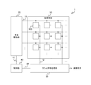
- FIG. 3 is a plan view showing a configuration example of an image sensor according to an embodiment of the present disclosure.
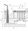
- FIG. 3 is a cross-sectional view showing a configuration example of the image sensor according to the first embodiment of the present disclosure.
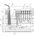
- FIG. 6 is a cross-sectional view showing another configuration example of the image sensor according to the first embodiment of the present disclosure.
- FIG. 1 is a diagram illustrating a configuration example of an imaging device according to an embodiment of the present disclosure.
- the image pickup device 9 in the figure includes an image pickup element 1, a bonding wire 7, adhesives 2, 4 and 6, a circuit board 3, a frame 5, and a cover glass 8.
- the image sensor 1 is a semiconductor element that converts incident light from a subject into an image signal.
- the image pickup device 1 is composed of a semiconductor chip. As will be described later, the image pickup device 1 is connected to the circuit board 3 by wire bonding.
- the circuit board 3 is a board on which the image pickup device 1 is mounted. On this circuit board 3, an electronic circuit that processes an image signal generated by the image sensor 1 and controls the image sensor 1 can be arranged. The image pickup device 1 is adhered to the circuit board 3 with an adhesive 2.
- the bonding wire 7 electrically connects the image pickup device 1 and the circuit board 3.
- the bonding wire 7 is made of, for example, a metal wire such as gold (Au), and is welded and connected to bonding pads (not shown) arranged on the image sensor 1 and the circuit board 3, respectively. This connection can be performed, for example, by the following procedure.
- the bonding wire 7 is passed through an instrument called a capillary, and the tip of the bonding wire 7 is made spherical by discharge heating. Next, the tip of the bonding wire 7 is heated and pressure-bonded to the bonding pad using a capillary. Thereby, wire bonding can be performed.
- connection strength by wire bonding can be evaluated by the ball shear strength.
- the ball shear strength is the shear strength of the bonding portion after connection, and can be measured by breaking (shearing) the connection portion with a dedicated inspection tool.
- the frame 5 is a housing that surrounds the image sensor 1.
- the frame 5 is bonded to the circuit board 3 with an adhesive 4.
- the cover glass 8 encloses the image sensor 1 and transmits incident light.
- the cover glass 8 is adhered to the frame 5 with an adhesive 6.
- FIG. 2 is a diagram illustrating a configuration example of the image sensor according to the embodiment of the present disclosure.
- the image sensor 1 of FIG. 1 includes an image capturing area 10, a vertical drive unit 20, a column signal processing unit 30, and a control unit 40.
- the imaging area 10 is an area in which the pixels 100 are arranged in a two-dimensional lattice.
- the pixel 100 produces
- the pixel 100 has a photoelectric conversion unit that generates electric charges according to the applied light.
- the pixel 100 further includes a pixel circuit. This pixel circuit generates an image signal based on the charges generated by the photoelectric conversion unit. Generation of the image signal is controlled by a control signal generated by the vertical drive unit 20 described later.
- the signal lines 11 and 12 are arranged in an XY matrix.
- the signal line 11 is a signal line that transmits a control signal of a pixel circuit in the pixel 100, is arranged for each row of the imaging region 10, and is commonly wired to the pixels 100 arranged in each row.
- the signal line 12 is a signal line for transmitting an image signal generated by the pixel circuit of the pixel 100, is arranged in each column of the imaging region 10, and is commonly wired to the pixels 100 arranged in each column. ..
- These photoelectric conversion units and pixel circuits are formed on a semiconductor substrate.
- the vertical drive unit 20 generates a control signal for the pixel circuit of the pixel 100.
- the vertical drive unit 20 transmits the generated control signal to the pixel 100 via the signal line 11 in the figure.
- the column signal processing unit 30 processes the image signal generated by the pixel 100.
- the column signal processing unit 30 processes the image signal transmitted from the pixel 100 via the signal line 12 in FIG.
- the processing in the column signal processing unit 30 corresponds to, for example, analog-digital conversion for converting an analog image signal generated in the pixel 100 into a digital image signal.
- the image signal processed by the column signal processing unit 30 is output as an image signal of the image sensor 1.
- the control unit 40 controls the entire image sensor 1.
- the control unit 40 controls the image sensor 1 by generating and outputting a control signal for controlling the vertical drive unit 20 and the column signal processing unit 30.
- the control signal generated by the control unit 40 is transmitted to the vertical drive unit 20 and the column signal processing unit 30 via the signal lines 41 and 42, respectively.
- FIG. 3 is a plan view showing a configuration example of the image sensor according to the embodiment of the present disclosure.
- This figure is a diagram showing a configuration of a light-receiving surface of the image sensor 1 to which incident light is irradiated.
- the image capturing area 10 described in FIG. 2 is arranged in the center.
- a peripheral pad region 60 where a bonding pad to which the bonding wire 7 is connected is arranged is arranged.
- the connection portion 71 which is a portion where the bonding wire 7 is connected to the bonding pad by wire bonding, is described.
- the bonding pad is arranged in the deep portion of the image sensor 1.
- An opening 161 reaching the bonding pad is formed on the light receiving surface of the image sensor 1. Wire bonding is performed through the opening 161 to form the connecting portion 71.
- an opening 171 is arranged adjacent to the opening 161.
- the opening 171 is an opening into which the inspection tool for ball shear strength described above is inserted.
- a scribe area 181 is arranged around the peripheral pad area 60.
- the scribe region 181 is a groove-shaped opening that is arranged around the semiconductor chip that constitutes the image sensor 1.
- the image pickup device 1 is formed by adjoining a plurality of image pickup devices on a semiconductor wafer and cutting the wafer into individual pieces.
- the scribe area 181 is an area where a blade for cutting is applied. By forming such an opening, the resin layer arranged in the image pickup device 1 can be deleted, and the cutting for individualization can be easily performed.
- peripheral pad region 60 and the scribe region 181 are arranged in the peripheral portion of the image sensor 1.
- FIG. 4 is a cross-sectional view showing a configuration example of the image sensor according to the first embodiment of the present disclosure.
- the figure shows a cross-sectional configuration of the image sensor 1 in the image capturing area 10, the peripheral pad area 60, and the scribe area 181.
- the configuration of the pixel 100 in the imaging region 10 will be described.
- the image pickup device 1 of FIG. 1 includes a semiconductor substrate 120, a wiring region 130, a support substrate 140, protective films 122, 124 and 126, a color filter 151, a light shielding film 152, a flattening film 153, and an on-chip. And a lens 154.
- the semiconductor substrate 120 is a semiconductor substrate on which the semiconductor element portions such as the photoelectric conversion unit of the pixel 100, the pixel circuit, and the vertical drive unit 20 described in FIG. 2 are arranged.
- the semiconductor substrate 120 can be made of, for example, silicon (Si).
- a semiconductor element such as a photoelectric conversion unit is formed in a well region formed on the semiconductor substrate 120.
- the semiconductor substrate 120 in the figure constitutes a p-type well region.
- the photoelectric conversion unit is described as an example of the semiconductor element.
- the photoelectric conversion section is composed of an n-type semiconductor region 121 in the figure and a pn junction formed between the p-type well regions around the n-type semiconductor region 121.
- This pn junction constitutes a photodiode and performs photoelectric conversion when irradiated with incident light.
- the n-type semiconductor region 121 is arranged for each pixel 100.
- the semiconductor substrate 120 can be configured to have a thickness of, for example, several ⁇ m to several tens of ⁇ m.
- the protective film 122 is a film that is disposed on the surface of the semiconductor substrate 120 and protects the semiconductor substrate 120.
- the protective film 122 can be made of, for example, silicon oxide (SiO 2 ).
- the protective film 124 is a film disposed on the back surface of the semiconductor substrate 120 and protecting the semiconductor substrate 120.
- the protective film 124 can be made of an inorganic material such as SiO 2 or silicon nitride (SiN) that transmits incident light.
- a separation region 125 is arranged between the pixels 100. The separation region 125 separates adjacent pixels 100 from each other.
- the isolation region 125 is arranged in a trench formed from the back surface side of the semiconductor substrate 120, can be made of the same material as the protective film 124, and can be formed at the same time as the protective film 124.
- the protective film 126 is a film that is disposed on the back surface of the semiconductor substrate 120 adjacent to the protective film 124 and protects the semiconductor substrate 120. Further, the protective film 126 further planarizes the back surface of the semiconductor substrate 120 on which the color filter 151 described later is formed.
- the protective film 126 for example, a film made of an organic material or an inorganic material that transmits incident light can be used.
- the protective films 122, 124, and 126 are examples of the protective film described in the claims.
- the wiring region 130 is a region where wiring for transmitting a signal of an element of the pixel 100 such as a photoelectric conversion unit is formed.
- the wiring region 130 is arranged on the front surface side of the semiconductor substrate 120. Specifically, it is arranged adjacent to the protective film 122.
- the wiring region 130 is configured by laminating a wiring layer in which the wiring 131 is formed and an insulating layer 132 that insulates the wiring 131. In the same figure, an example of a wiring region laminated in four layers is shown.
- the wirings 131 arranged in different layers are connected by the via plug 133.
- the wiring 131 can be made of, for example, a metal such as copper (Cu) or tungsten (W).
- the insulating layer 132 can be made of, for example, SiO 2 . Further, bonding pads 134, which will be described later, are arranged in the wiring region 130.
- the support substrate 140 is a substrate that is adhered to the wiring region 130 to support the image pickup device 1.
- the support substrate 140 is a substrate that improves the strength of the image sensor 1 in the manufacturing process of the image sensor 1.
- the color filter 151 is an optical filter that transmits light having a predetermined wavelength of incident light.
- the color filter 151 is arranged for each pixel 100.
- a color filter 151 that transmits any of red light, green light, and blue light can be used.
- the light shielding film 152 is a film that shields incident light.
- the light shielding film 152 is arranged at the boundary between the pixels 100 and blocks light transmitted through the color filters 151 of the adjacent pixels 100. Thereby, color mixture can be prevented.
- the flattening film 153 is a film for flattening the back surface of the semiconductor substrate 120 on which an on-chip lens 154 described later is formed.
- the flattening film 153 can be made of the same material as the on-chip lens 154.
- the on-chip lens 154 is a lens that is arranged for each pixel 100 and focuses incident light on the photoelectric conversion unit.
- the image pickup device 1 of the same figure corresponds to a backside illumination type image pickup device in which incident light is emitted from the backside which is a surface different from the surface on which the wiring region 130 of the semiconductor substrate 120 is arranged. ..
- Bonding pads 134 are arranged in the wiring region 130 of the peripheral pad region 60. Further, an opening 161 reaching the bonding pad 134 from the back surface of the image sensor 1 is formed. The bonding wire 7 is connected to the bonding pad 134 through the opening 161 to form the connecting portion 71.
- An opening 171 is arranged adjacent to this opening 161.
- the opening 171 opens from the flattening film 153 and the protective films 124 and 126 to the region of the semiconductor substrate 120.
- An inspection tool is inserted into the opening 171 to provide ball shear strength.
- the ball shear strength is measured by shearing the connecting portion 71 with an inspection tool.
- the shearing of the connecting portion 71 can be performed at a position which is 1 ⁇ 4 or less of the height of the connecting portion 71 from the head of the connecting portion 71. Therefore, the opening depth of the opening 171 can be made shallower than that of the opening 161.
- a convex portion 172 is arranged at the bottom of the opening 171.
- the convex portion 172 scatters the reflected light when the incident light is reflected at the bottom of the opening 171. Thereby, the influence of the reflected light on the opening 171 can be reduced. Details of the configuration of the convex portion 172 will be described later.
- the isolation region 125 is arranged similarly to the pixel region 10.
- the isolation region 125 in the peripheral pad region 60 is formed in the shape of a groove near the region where the bonding pad 134 is arranged, and insulates the semiconductor substrate 120 in the peripheral pad region 60. Further, the separation region 125 can eliminate the influence of the chipping of the semiconductor substrate 120 that has occurred in the scribe region 181.
- a scribe area 181 is arranged outside the peripheral pad area 60.
- the opening that forms the scribe region 181 can be formed simultaneously with the opening 171.
- FIG. 5 is a plan view showing a configuration example of the convex portion according to the first embodiment of the present disclosure.
- This figure is a diagram showing an arrangement example of the convex portions 172.
- the bonding pad 134 is arranged at the bottom and the connecting portion 71 of the bonding wire 7 is arranged.
- the semiconductor substrate 120 is arranged at the bottom of the adjacent openings 171, and the plurality of protrusions 172 are arranged at equal pitches.
- the convex portion 172 can be formed in a circular shape.
- the height of the convex portion 172 may be, for example, 0.2 to 4 ⁇ m.
- the convex portions 172 can be arranged at a pitch of 1 to 6 ⁇ m, for example.
- FIG. 6 is a diagram illustrating an example of reflection of incident light on the convex portion according to the first embodiment of the present disclosure.
- “a” represents the scattering of the reflected light by the convex portion 172.
- the white arrow indicates the incident light
- the solid arrow indicates the incident light reflected by the convex portion 172.
- the reflected light is scattered by the convex portion 172. Thereby, the reflectance in a specific direction can be reduced.
- the dotted line arrow represents the reflected light when the convex portion 172 is not arranged.
- the convex portion 172 When the convex portion 172 is not arranged, the incident light is not scattered but reflected at the bottom of the opening 171 and further reflected by the bonding wire 7 to become stray light. This stray light is incident on the imaging region 10 to generate flare. In this way, when the convex portion 172 is not arranged, for example, the reflectance in the direction toward the bonding wire 7 becomes high and the influence of the reflected light in that direction becomes large. Specifically, strong flare is generated near the bonding wire 7, and the image quality is degraded.
- b is a diagram showing the relationship between the wavelength of incident light and the reflectance when the convex portion 172 is arranged at the bottom of the opening 171.
- the horizontal axis of b in the figure represents the wavelength of the incident light.
- the unit is nm.
- the vertical axis of b in the figure represents the reflectance.
- the unit is%.
- the reflectance represents a ratio of reflected light having a reflection angle equal to the incident angle with respect to the incident light in the reflection at the bottom of the opening 171.
- the solid line graph of b in the figure represents the case where the incident angle is 60 degrees, and the dotted line graph represents the case where the incident angle is 30 degrees. It can be seen that the reflectance is less than 5% in both cases.
- FIG. 7 is a cross-sectional view showing another configuration example of the image sensor according to the first embodiment of the present disclosure.
- a substrate 200 is arranged instead of the support substrate 140.
- the substrate 200 is a substrate including a semiconductor substrate 220 and a wiring region 230.
- circuits other than the image pickup area 10 described in FIG. 2 can be arranged.
- only the imaging region 10 is arranged on the semiconductor substrate 120.
- the wiring region 230 is composed of the wiring 231 and the insulating layer 232, and is bonded to the wiring region 130.
- Protective films 136 and 236 are arranged in the wiring regions 130 and 230 on the bonding surface, respectively.
- the protective films 136 and 236 can be made of, for example, SiN.
- a protective film 253 is arranged on the surface of the semiconductor substrate 220.
- the signal transmission between the wiring region 130 and the wiring region 230 can be performed by the via plugs 165 and 166 and the wiring 167.
- the via plug 165 is a via plug formed to penetrate the semiconductor substrate 120 and the wiring region 130
- the via plug 166 is a via plug formed to penetrate the semiconductor substrate 120.
- the wiring 167 is a wiring formed on the protective film 126 on the back surface side of the semiconductor substrate 120 to electrically connect the via plugs 165 and 166.
- the bonding wire 7 is connected to the bonding pad 234 arranged in the wiring area 230.
- An opening 162 reaching the bonding pad 234 from the back surface of the image sensor 1 is formed.
- the bonding wire 7 is connected to the bonding pad 234 through the opening 162, and the connection portion 72 is formed.
- the opening 171 is arranged adjacent to the opening 162, and the protrusion 172 is arranged at the bottom of the opening 171.
- the image pickup device 1 in the figure further includes an intralayer lens 155 and a flattening film 156.
- the in-layer lens 155 is a lens that is arranged in the inner layer of the image sensor 1 and collects incident light.
- the in-layer lens 155 can be made of, for example, SiN.
- the flattening film 156 is a film that flattens the surface of the intralayer lens 155.
- the flattening film 156 can be made of resin, for example.
- the light shielding film 152 in the figure is formed so as to penetrate the flattening film 153, the in-layer lens 155 and the protective film 126.
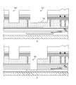
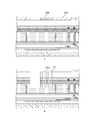
- FIG. 8 to 11 are diagrams showing an example of the method for manufacturing the image sensor according to the first embodiment of the present disclosure. 8 to 11 are diagrams showing a manufacturing process of the image pickup device 1 described in FIG.
- the well region and the n-type semiconductor region 121 are formed on the semiconductor substrate 120.
- the process corresponds to the imaging region forming process.
- a protective film 122 is formed on the surface of the semiconductor substrate 120, and the wiring regions 130 are arranged adjacent to each other. This step corresponds to the wiring area placement step.
- the protective film 124 is arranged. This step corresponds to the protective film disposing step (a in FIG. 8).
- a resist 301 is arranged on the surface of the protective film 124 and patterned (b in FIG. 8).
- the protective film 124 is etched using the resist 301 as a mask to form a patterned protective film 124a (c in FIG. 8).
- the protective film 126 is arranged on the surface of the protective film 124 (d in FIG. 9), and the light shielding film 152, the color filter 151, and the flattening film 153 are sequentially stacked.
- an on-chip lens 154 is formed on the surface of the flattening film 153 (e in FIG. 9).
- the resist 305 is placed on the surface of the on-chip lens 154.
- the opening 306 corresponding to the openings 161 and 171 described in FIG. 4 and the opening 307 corresponding to the scribe region 181 are formed (f in FIG. 9).
- the image sensor 1 is etched using the resist 305 as a mask. This etching is performed up to the region of the semiconductor substrate 120.
- the etching can be performed by dry etching.
- the opening 171 and the scribe region 181 are formed.
- a part of the opening 161 adjacent to the opening 171 is also formed.
- This step corresponds to the opening forming step.
- the shape of the patterned protective film 124a described in FIG. 9F is transferred to the semiconductor substrate 120 at the bottom of the opening 171, and the protrusion 172 is formed (g in FIG. 10).
- This step corresponds to the convex portion arranging step.
- the opening 161 is formed (h in FIG. 10). This can be formed by the same process as the opening 171.
- the semiconductor wafer is cut in the scribe region 181 to be separated into individual pieces (i in FIG. 11).
- the image pickup device 1 is bonded to the circuit board 3 (not shown), the bonding wires 7 are connected, and wire bonding is performed (j in FIG. 11).
- the image sensor 1 can be manufactured through the above steps.
- the convex portion 172 is arranged in the opening near the connecting portion 71 of the bonding wire 7, and the reflected light is scattered. As a result, reflection of incident light on the peripheral portion of the image sensor 1 is reduced, and deterioration of image quality can be prevented.
- FIG. 12 is a plan view showing a configuration example of a convex portion according to the second embodiment of the present disclosure.
- This figure shows variations in the planar shape of the convex portion 172.
- a represents an example of the rectangular convex portion 172a.
- b in the figure represents an example of the triangular convex portion 172b.
- the shape of the convex portion 172 may be another shape such as an octagon.
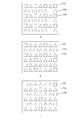
- FIG. 13 is a plan view showing another configuration example of the convex portion according to the second embodiment of the present disclosure.
- the figure shows an example in which the convex portion 172a and the convex portion 172b are arranged.
- a represents an example in which the convex portions 172a and the convex portions 172b are alternately arranged and arranged at equal pitches.
- b and c in the same figure represent an example in which the periodicity of the arrangement of the convex portions 172a and 172b is changed by making the arrangement of the convex portions 172a and 172b asymmetric. is there.
- the periodicity By changing the periodicity, it is possible to prevent the occurrence of interference fringes due to reflected light and prevent deterioration of image quality.
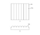
- FIG. 14 is a diagram showing another configuration example of the convex portion according to the second embodiment of the present disclosure.
- a is a plan view showing a configuration example of the convex portion
- b in the figure is a sectional view showing a configuration example of the convex portion.
- the figure shows an example in which a plurality of convex portions 172c configured in a kamaboko shape are arranged adjacent to each other.
- the kamaboko shape is a shape obtained by cutting a cylinder in half vertically.
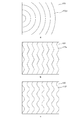
- FIG. 15 is a plan view showing another configuration example of the convex portion according to the second embodiment of the present disclosure.
- a represents an example of a kamaboko-shaped convex portion 172d arranged concentrically.
- b represents an example of a convex portion 172e having a zigzag shape and having a kamaboko-shaped cross section.
- c represents an example of a convex portion 172f having a kamaboko-shaped cross section and configured in a wave shape.
- FIG. 16 is a cross-sectional view showing another configuration example of the convex portion according to the second embodiment of the present disclosure.
- a represents an example of the convex portion 172g having a rectangular cross section.
- b represents an example of the convex portion 172h formed in a triangular pyramid.
- c represents an example of the convex portion 172i formed of the semiconductor substrate 120 and the protective film 124 and having a hemispherical shape.
- d represents an example of the convex portion 172j formed of the semiconductor substrate 120 and the protective film 124 and having a rectangular cross section.
- e represents an example of the convex portion 172k which is similarly formed in a triangular pyramid shape.
- the configuration of the image sensor 1 other than this is the same as the configuration of the image sensor 1 described in the first embodiment of the present disclosure, and thus the description thereof is omitted.
- the imaging device 1 can reduce the reflected light by using the convex portions 172a to 172k having a shape different from the convex portion 172.
- FIG. 17 is a diagram illustrating an example of the method for manufacturing the image sensor according to the third embodiment of the present disclosure. This figure is a diagram corresponding to the manufacturing process of the image pickup device 1 described with reference to f in FIG. 9 and g in FIG. 10.
- the back surface of the semiconductor substrate 120 is formed in a moth-eye shape with triangular pyramidal protrusions.
- the convex portion can be formed by depositing 111 planes by wet-etching 100 planes on the surface of the semiconductor substrate 120.
- the shape of this convex portion is transferred to the protective film 124 laminated on the semiconductor substrate 120 and is planarized by the protective film 126.
- FIG. 18 is a diagram showing another method for manufacturing the image sensor according to the third embodiment of the present disclosure.
- the resist 309 is arranged at the position where the convex portion 172 is arranged.
- etching is performed to form the convex portion 172m (g in the figure).
- FIG. 19 is a diagram showing another method for manufacturing the image pickup device according to the third embodiment of the present disclosure.
- a concave portion 308 is formed on the surface of the semiconductor substrate 120 at a position where the convex portion 172 is arranged, and the protective film 122 is embedded in the concave portion 308.
- etching is performed using the resist 305 as a mask to form a convex portion 137 formed of the protective film 122 (g in the figure).
- FIG. 20 is a diagram showing another method for manufacturing the image sensor according to the third embodiment of the present disclosure.
- the on-chip lens 157 is formed at a position where the convex portion 172 is arranged.
- etching is performed using the resist 305 as a mask to form a convex portion 172n in which the shape of the on-chip lens 157 is transferred to the semiconductor substrate 120 (g in the figure).
- the shape of the on-chip lens 157 may be transferred to the protective film 122 to form a convex portion.
- FIG. 21 is a diagram showing another method for manufacturing the image sensor according to the third embodiment of the present disclosure.
- a concave portion 310 is formed on the back surface of the semiconductor substrate 120 at a position where the convex portion 172 is arranged, and the protective film 124 is embedded in the concave portion 310.
- etching is performed using the resist 305 as a mask to form a convex portion 172o formed of the protective film 122 (g in the figure).
- the configuration of the image sensor 1 other than this is the same as the configuration of the image sensor 1 described in the first embodiment of the present disclosure, and thus the description thereof is omitted.
- the convex portion 172 can be formed by a manufacturing method different from that of the convex portion 172 described in FIG.
- the convex portion 172 is arranged in the opening near the connecting portion 71 of the bonding wire 7.
- the image sensor 1 according to the fourth embodiment of the present disclosure is different from the above-described first embodiment in that the convex portion is arranged in the scribe region 181.
- FIG. 22 is a cross-sectional view showing a configuration example of the image sensor according to the fourth embodiment of the present disclosure.
- the image pickup device 1 of the same drawing is different from the image pickup device 1 described in FIG. 4 in that a convex portion 182 is further arranged at the bottom of the scribe region 181.
- the convex portion 182 is a convex portion formed on the semiconductor substrate 120 similarly to the convex portion 172.
- the convex portion 182 is arranged in the scribe region 181, it is possible to scatter reflected light when the scribe region 181 is irradiated with incident light. Since the scribe region 181 is also arranged in the vicinity of the bonding wire 7, when the reflected light of the scribe region 181 is further reflected by the bonding wire 7, stray light increases. When this stray light enters the imaging region 10, the image quality deteriorates. However, by forming the convex portion 182 in the scribe region 181, it is possible to reduce the increase in stray light due to scattered reflected light.
- the configuration of the image sensor 1 is not limited to this example.
- the convex portion 172 may be omitted.
- a front-illuminated image pickup device can be used as the image pickup device 1.
- the configuration of the image sensor 1 other than this is the same as the configuration of the image sensor 1 described in the first embodiment of the present disclosure, and thus the description thereof is omitted.
- the reflected light in the scribe area 181 is scattered by disposing the convex portion 182. As a result, reflection of incident light on the peripheral portion of the image sensor 1 is reduced, and deterioration of image quality can be prevented.
- the technology according to the present disclosure (this technology) can be applied to various products.
- the present technology may be realized as an image pickup device mounted in an image pickup apparatus such as a camera.
- FIG. 23 is a block diagram showing a schematic configuration example of a camera which is an example of an imaging device to which the present technology can be applied.
- the camera 1000 in the figure includes a lens 1001, an image sensor 1002, an imaging control unit 1003, a lens driving unit 1004, an image processing unit 1005, an operation input unit 1006, a frame memory 1007, and a display unit 1008. And a recording unit 1009.
- the lens 1001 is a taking lens of the camera 1000.
- the lens 1001 collects light from a subject and makes it incident on an image sensor 1002 described later to form an image of the subject.
- the image pickup element 1002 is a semiconductor element that picks up light from a subject condensed by the lens 1001.
- the image sensor 1002 generates an analog image signal according to the emitted light, converts it into a digital image signal, and outputs it.
- the image capturing control unit 1003 controls image capturing by the image sensor 1002.
- the imaging control unit 1003 controls the imaging element 1002 by generating a control signal and outputting the control signal to the imaging element 1002.
- the imaging control unit 1003 can also perform autofocus in the camera 1000 based on the image signal output from the image sensor 1002.
- the auto focus is a system that detects the focal position of the lens 1001 and automatically adjusts it.
- a method (image plane phase difference autofocus) of detecting a focus position by detecting an image plane phase difference by a phase difference pixel arranged in the image sensor 1002 can be used. It is also possible to apply a method (contrast autofocus) of detecting the position where the contrast of the image is the highest as the focus position.
- the imaging control unit 1003 adjusts the position of the lens 1001 via the lens driving unit 1004 based on the detected focus position, and performs autofocus.
- the imaging control unit 1003 can be configured by, for example, a DSP (Digital Signal Processor) equipped with firmware.
- DSP Digital Signal Processor
- the lens driving unit 1004 drives the lens 1001 under the control of the imaging control unit 1003.
- the lens driving unit 1004 can drive the lens 1001 by changing the position of the lens 1001 using a built-in motor. ..
- the image processing unit 1005 processes the image signal generated by the image sensor 1002. This processing includes, for example, demosaic for generating image signals of insufficient colors among the image signals corresponding to red, green and blue for each pixel, noise reduction for removing noise of the image signals and encoding of the image signals. Applicable
- the image processing unit 1005 can be configured by, for example, a microcomputer equipped with firmware.
- the operation input unit 1006 receives an operation input from the user of the camera 1000.
- this operation input unit 1006 for example, a push button or a touch panel can be used.
- the operation input received by the operation input unit 1006 is transmitted to the imaging control unit 1003 and the image processing unit 1005. After that, a process according to the operation input, for example, a process of capturing an image of a subject is started.
- the frame memory 1007 is a memory that stores a frame that is an image signal for one screen.
- the frame memory 1007 is controlled by the image processing unit 1005 and holds frames in the process of image processing.
- the display unit 1008 displays the image processed by the image processing unit 1005.
- a liquid crystal panel can be used for the display unit 1008.
- the recording unit 1009 records the image processed by the image processing unit 1005.
- a memory card or a hard disk can be used.
- the present technology can be applied to the image sensor 1002 among the configurations described above.
- the imaging device 9 described in FIG. 1 can be applied to the imaging element 1002.
- the image pickup device 9 By applying the image pickup device 9 to the image pickup element 1002, it is possible to reduce the occurrence of flare and the like, and it is possible to prevent deterioration of the image quality of the image generated by the camera 1000.
- the camera has been described as an example, but the technique according to the present invention may be applied to other devices such as a monitoring device.
- FIG. 24 is a diagram showing an example of a schematic configuration of an endoscopic surgery system to which the technology according to the present disclosure can be applied.
- FIG. 24 illustrates a situation in which an operator (doctor) 11131 is performing an operation on a patient 11132 on a patient bed 11133 using the endoscopic operation system 11000.
- the endoscopic surgery system 11000 includes an endoscope 11100, other surgical tools 11110 such as a pneumoperitoneum tube 11111 and an energy treatment tool 11112, and a support arm device 11120 that supports the endoscope 11100.
- a cart 11200 on which various devices for endoscopic surgery are mounted.
- the endoscope 11100 includes a lens barrel 11101 into which a region of a predetermined length from the distal end is inserted into the body cavity of the patient 11132, and a camera head 11102 connected to the base end of the lens barrel 11101.
- the endoscope 11100 configured as a so-called rigid endoscope having the rigid barrel 11101 is illustrated, but the endoscope 11100 may be configured as a so-called flexible mirror having a flexible barrel. Good.
- An opening in which an objective lens is fitted is provided at the tip of the lens barrel 11101.
- a light source device 11203 is connected to the endoscope 11100, and the light generated by the light source device 11203 is guided to the tip of the lens barrel by a light guide extending inside the lens barrel 11101. It is irradiated toward the observation target in the body cavity of the patient 11132 via the lens.
- the endoscope 11100 may be a direct-viewing endoscope, or may be a perspective or side-viewing endoscope.
- An optical system and an image pickup device are provided inside the camera head 11102, and the reflected light (observation light) from the observation target is condensed on the image pickup device by the optical system.
- the observation light is photoelectrically converted by the imaging element, and an electric signal corresponding to the observation light, that is, an image signal corresponding to the observation image is generated.
- the image signal is transmitted as RAW data to a camera control unit (CCU: Camera Control Unit) 11201.
- CCU Camera Control Unit
- the CCU 11201 is composed of a CPU (Central Processing Unit), a GPU (Graphics Processing Unit), and the like, and centrally controls the operations of the endoscope 11100 and the display device 11202. Further, the CCU 11201 receives the image signal from the camera head 11102, and performs various image processing such as development processing (demosaic processing) on the image signal for displaying an image based on the image signal.
- image processing such as development processing (demosaic processing)
- the display device 11202 displays an image based on the image signal subjected to the image processing by the CCU 11201 under the control of the CCU 11201.
- the light source device 11203 is composed of a light source such as an LED (Light Emitting Diode), and supplies the endoscope 11100 with irradiation light when imaging a surgical site or the like.
- a light source such as an LED (Light Emitting Diode)
- LED Light Emitting Diode
- the input device 11204 is an input interface for the endoscopic surgery system 11000.
- the user can input various kinds of information and instructions to the endoscopic surgery system 11000 via the input device 11204.
- the user inputs an instruction to change the imaging conditions (type of irradiation light, magnification, focal length, etc.) by the endoscope 11100.
- the treatment instrument control device 11205 controls driving of the energy treatment instrument 11112 for cauterization of tissue, incision, sealing of blood vessel, or the like.
- the pneumoperitoneum device 11206 is used to inflate the body cavity of the patient 11132 through the pneumoperitoneum tube 11111 in order to inflate the body cavity of the patient 11132 for the purpose of securing the visual field by the endoscope 11100 and the working space of the operator.
- the recorder 11207 is a device capable of recording various information regarding surgery.
- the printer 11208 is a device capable of printing various information regarding surgery in various formats such as text, images, and graphs.
- the light source device 11203 that supplies irradiation light to the endoscope 11100 when imaging a surgical site can be configured by, for example, an LED, a laser light source, or a white light source configured by a combination thereof.
- a white light source is formed by a combination of RGB laser light sources
- the output intensity and output timing of each color (each wavelength) can be controlled with high accuracy, so that the light source device 11203 adjusts the white balance of the captured image. It can be carried out.
- the laser light from each of the RGB laser light sources is time-divided to the observation target, and the drive of the image pickup device of the camera head 11102 is controlled in synchronization with the irradiation timing, so that each of the RGB colors can be handled. It is also possible to take the captured image in time division. According to this method, a color image can be obtained without providing a color filter on the image sensor.
- the drive of the light source device 11203 may be controlled so as to change the intensity of the output light at predetermined time intervals.
- the driving of the image sensor of the camera head 11102 in synchronization with the timing of changing the intensity of the light to acquire images in a time-division manner and synthesizing the images, a high dynamic image without so-called blackout and overexposure is obtained. An image of the range can be generated.
- the light source device 11203 may be configured to be able to supply light in a predetermined wavelength band corresponding to special light observation.
- the special light observation for example, the wavelength dependence of the absorption of light in body tissues is used to irradiate a narrow band of light as compared with the irradiation light (that is, white light) at the time of normal observation, so that the mucosal surface layer
- the so-called narrow band imaging is performed in which a predetermined tissue such as blood vessels is imaged with high contrast.
- fluorescence observation in which an image is obtained by fluorescence generated by irradiating the excitation light may be performed.
- the body tissue is irradiated with excitation light to observe the fluorescence from the body tissue (autofluorescence observation), or a reagent such as indocyanine green (ICG) is locally injected into the body tissue and the body tissue is also injected.
- the excitation light corresponding to the fluorescence wavelength of the reagent can be irradiated to obtain a fluorescence image and the like.
- the light source device 11203 can be configured to be capable of supplying narrowband light and / or excitation light compatible with such special light observation.
- FIG. 25 is a block diagram showing an example of the functional configuration of the camera head 11102 and the CCU 11201 shown in FIG.
- the camera head 11102 includes a lens unit 11401, an imaging unit 11402, a driving unit 11403, a communication unit 11404, and a camera head control unit 11405.
- the CCU 11201 has a communication unit 11411, an image processing unit 11412, and a control unit 11413.
- the camera head 11102 and the CCU 11201 are communicably connected to each other via a transmission cable 11400.
- the lens unit 11401 is an optical system provided at the connecting portion with the lens barrel 11101.
- the observation light taken in from the tip of the lens barrel 11101 is guided to the camera head 11102 and enters the lens unit 11401.
- the lens unit 11401 is configured by combining a plurality of lenses including a zoom lens and a focus lens.
- the image pickup unit 11402 is composed of an image pickup element.
- the number of image pickup elements forming the image pickup section 11402 may be one (so-called single-plate type) or plural (so-called multi-plate type).
- image signals corresponding to RGB are generated by each image pickup element, and a color image may be obtained by combining them.
- the image capturing unit 11402 may be configured to have a pair of image capturing elements for respectively acquiring image signals for the right eye and the image for the left eye corresponding to 3D (Dimensional) display.
- the 3D display enables the operator 11131 to more accurately understand the depth of the living tissue in the operation site.
- a plurality of lens units 11401 may be provided corresponding to each image pickup element.
- the image pickup unit 11402 does not necessarily have to be provided in the camera head 11102.
- the imaging unit 11402 may be provided inside the lens barrel 11101 immediately after the objective lens.
- the drive unit 11403 is composed of an actuator, and moves the zoom lens and the focus lens of the lens unit 11401 by a predetermined distance along the optical axis under the control of the camera head control unit 11405. As a result, the magnification and focus of the image captured by the image capturing unit 11402 can be adjusted appropriately.
- the communication unit 11404 is composed of a communication device for transmitting and receiving various information to and from the CCU11201.
- the communication unit 11404 transmits the image signal obtained from the imaging unit 11402 as RAW data to the CCU 11201 via the transmission cable 11400.
- the communication unit 11404 receives a control signal for controlling the driving of the camera head 11102 from the CCU 11201 and supplies it to the camera head control unit 11405.
- the control signal includes, for example, information that specifies the frame rate of the captured image, information that specifies the exposure value at the time of capturing, and / or information that specifies the magnification and focus of the captured image. Contains information about the condition.
- the image capturing conditions such as the frame rate, the exposure value, the magnification, and the focus may be appropriately designated by the user, or may be automatically set by the control unit 11413 of the CCU 11201 based on the acquired image signal. Good. In the latter case, the so-called AE (Auto Exposure) function, AF (Auto Focus) function, and AWB (Auto White Balance) function are mounted on the endoscope 11100.
- the camera head control unit 11405 controls driving of the camera head 11102 based on a control signal from the CCU 11201 received via the communication unit 11404.
- the communication unit 11411 is composed of a communication device for transmitting and receiving various information to and from the camera head 11102.
- the communication unit 11411 receives the image signal transmitted from the camera head 11102 via the transmission cable 11400.
- the communication unit 11411 transmits a control signal for controlling the driving of the camera head 11102 to the camera head 11102.
- the image signal and the control signal can be transmitted by electric communication, optical communication, or the like.
- the image processing unit 11412 performs various types of image processing on the image signal that is the RAW data transmitted from the camera head 11102.
- the control unit 11413 performs various controls regarding imaging of a surgical site or the like by the endoscope 11100 and display of a captured image obtained by imaging the surgical site or the like. For example, the control unit 11413 generates a control signal for controlling the driving of the camera head 11102.
- control unit 11413 causes the display device 11202 to display a captured image of the surgical site or the like based on the image signal subjected to the image processing by the image processing unit 11412.
- the control unit 11413 may recognize various objects in the captured image using various image recognition techniques.
- the control unit 11413 detects a surgical instrument such as forceps, a specific body part, bleeding, and a mist when the energy treatment instrument 11112 is used by detecting the shape and color of the edge of the object included in the captured image. Can be recognized.
- the control unit 11413 may superimpose and display various types of surgery support information on the image of the operation unit using the recognition result. By displaying the surgery support information in a superimposed manner and presenting it to the operator 11131, the burden on the operator 11131 can be reduced, and the operator 11131 can proceed with the operation reliably.
- a transmission cable 11400 that connects the camera head 11102 and the CCU 11201 is an electric signal cable compatible with electric signal communication, an optical fiber compatible with optical communication, or a composite cable of these.
- wired communication is performed using the transmission cable 11400, but communication between the camera head 11102 and the CCU 11201 may be performed wirelessly.
- the technology according to the present disclosure can be applied to the imaging unit 11402 among the configurations described above.
- the imaging device 9 described in FIG. 1 can be applied to the imaging unit 10402.
- the technology according to the present disclosure can be applied to various products.
- the technology according to the present disclosure is realized as a device mounted on any type of moving body such as an automobile, an electric vehicle, a hybrid electric vehicle, a motorcycle, a bicycle, a personal mobility, an airplane, a drone, a ship, and a robot. May be.
- FIG. 26 is a block diagram showing a schematic configuration example of a vehicle control system which is an example of a mobile body control system to which the technology according to the present disclosure can be applied.
- the vehicle control system 12000 includes a plurality of electronic control units connected via a communication network 12001.
- the vehicle control system 12000 includes a drive system control unit 12010, a body system control unit 12020, a vehicle exterior information detection unit 12030, a vehicle interior information detection unit 12040, and an integrated control unit 12050.
- a microcomputer 12051, an audio / video output unit 12052, and an in-vehicle network I / F (interface) 12053 are shown as the functional configuration of the integrated control unit 12050.
- the drive system control unit 12010 controls the operation of devices related to the drive system of the vehicle according to various programs.
- the drive system control unit 12010 includes a drive force generation device for generating a drive force of a vehicle such as an internal combustion engine or a drive motor, a drive force transmission mechanism for transmitting the drive force to wheels, and a steering angle of the vehicle. It functions as a steering mechanism for adjusting and a control device such as a braking device for generating a braking force of the vehicle.
- the body system control unit 12020 controls the operation of various devices mounted on the vehicle body according to various programs.
- the body system control unit 12020 functions as a keyless entry system, a smart key system, a power window device, or a control device for various lamps such as a head lamp, a back lamp, a brake lamp, a winker, or a fog lamp.
- the body system control unit 12020 can be input with radio waves or signals of various switches transmitted from a portable device that substitutes for a key.
- the body system control unit 12020 receives input of these radio waves or signals and controls the vehicle door lock device, power window device, lamp, and the like.
- the vehicle exterior information detection unit 12030 detects information outside the vehicle equipped with the vehicle control system 12000.
- the image pickup unit 12031 is connected to the vehicle exterior information detection unit 12030.
- the vehicle exterior information detection unit 12030 causes the image capturing unit 12031 to capture an image of the vehicle exterior and receives the captured image.
- the vehicle exterior information detection unit 12030 may perform object detection processing or distance detection processing such as people, vehicles, obstacles, signs, or characters on the road surface based on the received image.
- the image pickup unit 12031 is an optical sensor that receives light and outputs an electric signal according to the amount of received light.
- the image pickup unit 12031 can output the electric signal as an image or as distance measurement information.
- the light received by the imaging unit 12031 may be visible light or invisible light such as infrared light.
- the in-vehicle information detection unit 12040 detects in-vehicle information.
- a driver state detection unit 12041 that detects the state of the driver is connected.
- the driver state detection unit 12041 includes, for example, a camera that images the driver, and the in-vehicle information detection unit 12040 determines the degree of fatigue or concentration of the driver based on the detection information input from the driver state detection unit 12041. It may be calculated or it may be determined whether or not the driver is asleep.
- the microcomputer 12051 calculates the control target value of the driving force generation device, the steering mechanism or the braking device based on the information on the inside and outside of the vehicle acquired by the outside information detection unit 12030 or the inside information detection unit 12040, and the drive system control unit.
- a control command can be output to 12010.
- the microcomputer 12051 realizes functions of ADAS (Advanced Driver Assistance System) including collision avoidance or impact mitigation of a vehicle, follow-up traveling based on an inter-vehicle distance, vehicle speed maintenance traveling, a vehicle collision warning, or a vehicle lane departure warning. It is possible to perform cooperative control for the purpose.
- ADAS Advanced Driver Assistance System
- the microcomputer 12051 controls the driving force generation device, the steering mechanism, the braking device, or the like on the basis of the information around the vehicle acquired by the vehicle exterior information detection unit 12030 or the vehicle interior information detection unit 12040, so that the driver's It is possible to perform cooperative control for the purpose of autonomous driving or the like that autonomously travels without depending on the operation.
- the microcomputer 12051 can output a control command to the body system control unit 12020 based on the information outside the vehicle acquired by the outside information detection unit 12030.
- the microcomputer 12051 controls the headlamp according to the position of the preceding vehicle or the oncoming vehicle detected by the vehicle exterior information detection unit 12030, and performs cooperative control for the purpose of antiglare such as switching the high beam to the low beam. It can be carried out.
- the voice image output unit 12052 transmits an output signal of at least one of a voice and an image to an output device capable of visually or audibly notifying information to an occupant of the vehicle or the outside of the vehicle.
- an audio speaker 12061, a display unit 12062, and an instrument panel 12063 are illustrated as output devices.
- the display unit 12062 may include at least one of an on-board display and a head-up display, for example.
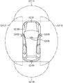
- FIG. 27 is a diagram showing an example of the installation position of the imaging unit 12031.
- the vehicle 12100 has imaging units 12101, 12102, 12103, 12104, 12105 as the imaging unit 12031.
- the image capturing units 12101, 12102, 12103, 12104, and 12105 are provided, for example, at positions such as the front nose of the vehicle 12100, the side mirrors, the rear bumper, the back door, and the upper portion of the windshield inside the vehicle.
- the image capturing unit 12101 provided on the front nose and the image capturing unit 12105 provided on the upper part of the windshield in the vehicle interior mainly acquire images in front of the vehicle 12100.
- the image capturing units 12102 and 12103 provided in the side mirrors mainly acquire images of the side of the vehicle 12100.
- the image capturing unit 12104 provided in the rear bumper or the back door mainly acquires an image behind the vehicle 12100.
- the front images acquired by the image capturing units 12101 and 12105 are mainly used for detecting a preceding vehicle, a pedestrian, an obstacle, a traffic signal, a traffic sign, a lane, or the like.
- FIG. 27 shows an example of the shooting range of the imaging units 12101 to 12104.
- the imaging range 12111 indicates the imaging range of the imaging unit 12101 provided on the front nose
- the imaging ranges 12112 and 12113 indicate the imaging ranges of the imaging units 12102 and 12103 provided on the side mirrors
- the imaging range 12114 indicates The imaging range of the imaging part 12104 provided in a rear bumper or a back door is shown. For example, by overlaying the image data captured by the image capturing units 12101 to 12104, a bird's-eye view image of the vehicle 12100 viewed from above can be obtained.
- At least one of the imaging units 12101 to 12104 may have a function of acquiring distance information.
- at least one of the image capturing units 12101 to 12104 may be a stereo camera including a plurality of image capturing elements or may be an image capturing element having pixels for phase difference detection.
- the microcomputer 12051 based on the distance information obtained from the imaging units 12101 to 12104, the distance to each three-dimensional object within the imaging range 12111 to 12114 and the temporal change of this distance (relative speed with respect to the vehicle 12100).
- the closest three-dimensional object on the traveling path of the vehicle 12100 which travels in the substantially same direction as the vehicle 12100 at a predetermined speed (for example, 0 km / h or more), can be extracted as a preceding vehicle. it can.
- the microcomputer 12051 can set an inter-vehicle distance to be secured in advance before the preceding vehicle, and can perform automatic brake control (including follow-up stop control), automatic acceleration control (including follow-up start control), and the like. In this way, it is possible to perform cooperative control for the purpose of autonomous driving, which autonomously travels without depending on the operation of the driver.
- the microcomputer 12051 uses the distance information obtained from the image capturing units 12101 to 12104 to convert three-dimensional object data regarding a three-dimensional object to other three-dimensional objects such as two-wheeled vehicles, ordinary vehicles, large vehicles, pedestrians, telephone poles, and the like. It can be classified, extracted, and used for automatic avoidance of obstacles. For example, the microcomputer 12051 distinguishes obstacles around the vehicle 12100 into obstacles visible to the driver of the vehicle 12100 and obstacles difficult to see. Then, the microcomputer 12051 determines the collision risk indicating the risk of collision with each obstacle, and when the collision risk is equal to or more than the set value and there is a possibility of collision, the microcomputer 12051 outputs the audio through the audio speaker 12061 and the display unit 12062. A driver can be assisted for avoiding a collision by outputting an alarm to the driver and performing forced deceleration or avoidance steering through the drive system control unit 12010.
- At least one of the image capturing units 12101 to 12104 may be an infrared camera that detects infrared rays.
- the microcomputer 12051 can recognize a pedestrian by determining whether or not the pedestrian is present in the images captured by the imaging units 12101 to 12104. To recognize such a pedestrian, for example, a procedure for extracting a feature point in an image captured by the image capturing units 12101 to 12104 as an infrared camera and pattern matching processing on a series of feature points indicating the contour of an object are performed to determine whether or not the pedestrian is a pedestrian.
- the audio image output unit 12052 causes the recognized pedestrian to have a rectangular contour line for emphasis.
- the display unit 12062 is controlled so as to superimpose. Further, the audio image output unit 12052 may control the display unit 12062 to display an icon indicating a pedestrian or the like at a desired position.
- the technology according to the present disclosure can be applied to the image capturing unit 12031 and the like among the configurations described above.
- the imaging device 9 described in FIG. 1 can be applied to the imaging unit 12031.
- drawings in the above-described embodiments are schematic, and the dimensional ratios of the respective parts and the like do not necessarily match the actual ones. Moreover, it is needless to say that the drawings may include portions having different dimensional relationships and ratios.
- the present technology may have the following configurations.
- An imaging region in which a photoelectric conversion unit that is formed on a semiconductor substrate and photoelectrically converts incident light is arranged;
- a wiring region having a wiring for transmitting a signal of the photoelectric conversion unit and arranged adjacent to the surface of the semiconductor substrate;
- a protective film which is arranged on a back surface which is a surface different from the front surface of the semiconductor substrate and which transmits the incident light and protects the back surface of the semiconductor,
- An opening that is arranged in an outer peripheral region of the imaging region and opens from the protective film to any region of the semiconductor substrate and the wiring region,
- An image pickup device comprising: a convex portion arranged at the bottom of the opening.
- the image pickup device wherein the opening is arranged in the wiring region and is arranged in the vicinity of a connection part used for connection to the outside.
- the image pickup device wherein the opening is a scribe region when the own image pickup device formed on a semiconductor wafer is singulated.
- the image sensor according to any one of (1) to (3), wherein the convex portion is configured by at least one of the semiconductor substrate, the wiring region, and the protective film.
- the convex portion is formed by the wiring region arranged in a concave portion formed on the surface of the semiconductor substrate before the wiring region is arranged.
- An on-chip lens that is disposed adjacent to the protective film and focuses the incident light on the photoelectric conversion unit is further included.
- the convex portion is formed by the protective film arranged in a concave portion formed on the back surface of the semiconductor substrate before the protective film is arranged. The image sensor described.
Landscapes
- Solid State Image Pick-Up Elements (AREA)
Abstract
撮像素子の周縁部における入射光の反射を軽減し、画質の低下を防止する。 撮像素子は、半導体基板に配置される撮像領域、配線領域、保護膜および半導体基板に形成される開口部の底部に配置される凸部を具備する。撮像領域は、半導体基板に形成されて入射光の光電変換を行う光電変換部が配置される。配線領域は、光電変換部の信号を伝達する配線を有するとともに半導体基板の表面に隣接して配置される。保護膜は、半導体基板の表面とは異なる面である裏面に配置されて入射光を透過させるとともに半導体の裏面を保護する。開口部は、撮像領域の外周領域に配置されて保護膜から半導体基板および配線領域の何れかの領域までに開口する。凸部は、開口部の底部に配置される。
Description
本開示は、撮像素子および撮像素子の製造方法に関する。詳しくは、ボンディングワイヤ近傍またはスクライブ領域において開口部が形成された撮像素子および当該撮像素子の製造方法に関する。
従来、素子表面における入射光の反射を軽減する撮像素子が使用されている。反射光によるフレアの発生を軽減し、画質の低下を防止するためである。例えば、撮像素子を構成する半導体基板の受光面にモスアイ形状の凹凸を形成し、入射光の反射を防止する撮像素子が提案されている(例えば、特許文献1参照。)。この撮像素子は、光電変換機能を有する受光部を含む画素が複数配置される画素領域に凹凸が形成され、入射光の反射を防止する。この凹凸の形成は、半導体基板の表面における100面をウェットエッチングすることにより111面を析出させ、四角錐形状の凸部を形成することにより行うことができる。
上述の従来技術では、画素領域以外の領域である周縁部に凹凸を形成することができず、当該領域における入射光の反射を軽減することができないという問題がある。半導体基板の裏面側に入射光が照射される裏面照射型の撮像素子においては、撮像素子および外部の基板等との接続を行うボンディングワイヤが撮像素子の深部に配置されたパッドに接続される。パッドの近傍には開口部が形成され、この開口部を介してボンディングワイヤが接続される。通常、パッドに接続されたボンディングワイヤの接着強度を測定する試験装置を挿入するため、パッドと略同等の深度の開口部が接続部に隣接して形成される。この試験用の開口部において、入射光の反射を生じると、反射光がボンディングワイヤによりさらに反射されて撮像素子に入射し、フレアを生じる。
また、撮像素子は、半導体ウェハに形成された複数の撮像素子が個片化されて製造される。この個片化は、複数の撮像素子の境界に形成された開口部(溝)に沿って半導体ウェハを切断することにより行うことができる。この開口部においても入射光の反射を生じる。このように、上述の従来技術では、撮像素子の周縁部における入射光の反射を防ぐことができず、画質の低下を防止することができないという問題がある。
本開示は、上述した問題点に鑑みてなされたものであり、撮像素子の周縁部における入射光の反射を軽減し、画質の低下を防止することを目的としている。
本開示は、上述の問題点を解消するためになされたものであり、その第1の態様は、半導体基板に形成されて入射光の光電変換を行う光電変換部が配置される撮像領域と、上記光電変換部の信号を伝達する配線を有するとともに上記半導体基板の表面に隣接して配置される配線領域と、上記半導体基板の表面とは異なる面である裏面に配置されて上記入射光を透過させるとともに上記半導体の裏面を保護する保護膜と、上記撮像領域の外周領域に配置されて上記保護膜から上記半導体基板および上記配線領域の何れかの領域までに開口する開口部と、上記開口部の底部に配置される凸部とを具備する撮像素子である。
また、この第1の態様において、上記開口部は、上記配線領域に配置されて外部との接続に使用される接続部の近傍に配置されてもよい。
また、この第1の態様において、上記開口部は、半導体ウェハに形成された自身の撮像素子を個片化する際のスクライブ領域であってもよい。
また、この第1の態様において、上記凸部は、上記半導体基板、上記配線領域および上記保護膜の少なくとも1つにより構成されてもよい。
また、この第1の態様において、上記凸部は、パターニングされた上記保護膜の形状が上記半導体基板および上記配線領域の何れかに転写されて形成されてもよい。
また、この第1の態様において、上記凸部は、上記パターニングされた保護膜をマスクとしてエッチングを行うことにより上記転写されて形成されてもよい。
また、この第1の態様において、上記凸部は、上記保護膜が配置される前の上記半導体基板の裏面に形成され、上記配置された保護膜を上記半導体基板まで開口することにより上記開口部の底部に配置されてもよい。
また、この第1の態様において、上記凸部は、上記保護膜に形成されたレジストをマスクとして上記保護膜および上記半導体基板をエッチングすることにより形成されてもよい。
また、この第1の態様において、上記凸部は、上記配線領域が配置される前の上記半導体基板の表面に形成された凹部に配置される上記配線領域により構成されてもよい。
また、この第1の態様において、上記保護膜に隣接して配置されて上記光電変換部に上記入射光を集光するオンチップレンズをさらに具備し、上記凸部は、上記オンチップレンズの形状が上記半導体基板および上記配線領域の何れかに転写されて形成されてもよい。
また、この第1の態様において、上記凸部は、上記保護膜が配置される前の上記半導体基板の裏面に形成された凹部に配置される上記保護膜により構成されてもよい。
また、本開示の第2の態様は、入射光の光電変換を行う光電変換部が配置される撮像領域を半導体基板に形成する撮像領域形成工程と、上記光電変換部の信号を伝達する配線を有する配線領域を上記半導体基板の表面に隣接して配置する配線領域配置工程と、上記半導体基板の表面とは異なる面である裏面に配置されて上記入射光を透過させるとともに上記半導体の裏面を保護する保護膜を配置する保護膜配置工程と、上記撮像領域の外周領域に配置されて上記保護膜から上記半導体基板および上記配線領域の何れかの領域までに開口する開口部を形成する開口部形成工程と、上記開口部の底部に凸部を配置する凸部配置工程とを具備する撮像素子の製造方法である。
上述の態様を採ることにより、開口部の底部に凸部が配置されるという作用をもたらす。凸部による入射光の散乱が想定される。
本開示によれば、撮像素子の周縁部における入射光の反射を軽減し、画質の低下を防止するという優れた効果を奏する。
次に、図面を参照して、本開示を実施するための形態(以下、実施の形態と称する)を説明する。以下の図面において、同一または類似の部分には同一または類似の符号を付している。また、以下の順序で実施の形態の説明を行う。
1.第1の実施の形態
2.第2の実施の形態
3.第3の実施の形態
4.第4の実施の形態
5.カメラへの応用例
6.内視鏡手術システムへの応用例
7.移動体への応用例
1.第1の実施の形態
2.第2の実施の形態
3.第3の実施の形態
4.第4の実施の形態
5.カメラへの応用例
6.内視鏡手術システムへの応用例
7.移動体への応用例
<1.第1の実施の形態>
[撮像素子の構成]
図1は、本開示の実施の形態に係る撮像装置の構成例を示す図である。同図の撮像装置9は、撮像素子1と、ボンディングワイヤ7と、接着剤2、4および6と、回路基板3と、フレーム5と、カバーガラス8とを備える。
[撮像素子の構成]
図1は、本開示の実施の形態に係る撮像装置の構成例を示す図である。同図の撮像装置9は、撮像素子1と、ボンディングワイヤ7と、接着剤2、4および6と、回路基板3と、フレーム5と、カバーガラス8とを備える。
撮像素子1は、被写体からの入射光を画像信号に変換する半導体素子である。この撮像素子1は、半導体チップにより構成される。後述するように、撮像素子1は、ワイヤボンディングにより回路基板3に接続される。
回路基板3は、撮像素子1が実装される基板である。この回路基板3には、撮像素子1により生成された画像信号の処理や撮像素子1の制御を行う電子回路を配置することができる。撮像素子1は、接着剤2により回路基板3に接着される。
ボンディングワイヤ7は、撮像素子1および回路基板3の間を電気的に接続するものである。このボンディングワイヤ7は、例えば、金(Au)等の金属の線により構成され、撮像素子1および回路基板3のそれぞれに配置されたボンディングパッド(不図示)に溶着されて接続される。この接続は、例えば、次の手順により行うことができる。キャピラリーと称される器具にボンディングワイヤ7を通し、放電加熱によりボンディングワイヤ7の先端部を球状にする。次に、キャピラリーを使用してボンディングワイヤ7の先端部をボンディングパッドに加熱圧接する。これにより、ワイヤボンディングを行うことができる。
なお、ワイヤボンディングによる接続強度は、ボールシェア強度により評価することができる。ここで、ボールシェア強度とは、接続後のボンディング部分のせん断強度であり、専用の検査器具により接続部を破壊(せん断)することにより測定することができる。
フレーム5は、撮像素子1を囲繞する筐体である。このフレーム5は、接着剤4により回路基板3に接着される。カバーガラス8は、撮像素子1を封入するとともに入射光を透過させるものである。このカバーガラス8は、接着剤6によりフレーム5に接着される。
[撮像素子の構成]
図2は、本開示の実施の形態に係る撮像素子の構成例を示す図である。同図の撮像素子1は、撮像領域10と、垂直駆動部20と、カラム信号処理部30と、制御部40とを備える。
図2は、本開示の実施の形態に係る撮像素子の構成例を示す図である。同図の撮像素子1は、撮像領域10と、垂直駆動部20と、カラム信号処理部30と、制御部40とを備える。
撮像領域10は、画素100が2次元格子状に配置される領域である。ここで、画素100は、照射された光に応じた画像信号を生成するものである。この画素100は、照射された光に応じた電荷を生成する光電変換部を有する。また画素100は、画素回路をさらに有する。この画素回路は、光電変換部により生成された電荷に基づく画像信号を生成する。画像信号の生成は、後述する垂直駆動部20により生成された制御信号により制御される。撮像領域10には、信号線11および12がXYマトリクス状に配置される。信号線11は、画素100における画素回路の制御信号を伝達する信号線であり、撮像領域10の行毎に配置され、各行に配置される画素100に対して共通に配線される。信号線12は、画素100の画素回路により生成された画像信号を伝達する信号線であり、撮像領域10の列毎に配置され、各列に配置される画素100に対して共通に配線される。これら光電変換部および画素回路は、半導体基板に形成される。
垂直駆動部20は、画素100の画素回路の制御信号を生成するものである。この垂直駆動部20は、生成した制御信号を同図の信号線11を介して画素100に伝達する。カラム信号処理部30は、画素100により生成された画像信号を処理するものである。このカラム信号処理部30は、同図の信号線12を介して画素100から伝達された画像信号の処理を行う。カラム信号処理部30における処理には、例えば、画素100において生成されたアナログの画像信号をデジタルの画像信号に変換するアナログデジタル変換が該当する。カラム信号処理部30により処理された画像信号は、撮像素子1の画像信号として出力される。制御部40は、撮像素子1の全体を制御するものである。この制御部40は、垂直駆動部20およびカラム信号処理部30を制御する制御信号を生成して出力することにより、撮像素子1の制御を行う。制御部40により生成された制御信号は、信号線41および42により垂直駆動部20およびカラム信号処理部30に対してそれぞれ伝達される。
図3は、本開示の実施の形態に係る撮像素子の構成例を示す平面図である。同図は、撮像素子1における入射光が照射される受光面の構成を表す図である。同図の撮像素子1の受光面には、図2において説明した撮像領域10が中央部に配置される。撮像領域10の周囲には、ボンディングワイヤ7が接続されるボンディングパッドが配置される周辺パッド領域60が配置される。同図においては、ワイヤボンディングによりボンディングワイヤ7がボンディングパッドに接続される部分である接続部71を記載した。後述するように、ボンディングパッドは、撮像素子1の深部に配置される。撮像素子1の受光面には、ボンディングパッドに達する開口部161が形成される。この開口部161を介してワイヤボンディングが行われ、接続部71が形成される。なお、同図の撮像素子1には、開口部161に隣接して開口部171が配置される。この開口部171は、前述したボールシェア強度のための検査器具を挿入する開口部である。
周辺パッド領域60の周囲にはスクライブ領域181が配置される。このスクライブ領域181は、撮像素子1を構成する半導体チップの周辺に配置される溝状の開口部である。撮像素子1は、半導体ウェハに複数の撮像素子が隣接して形成され、切断されて個片化される。スクライブ領域181は、切断のためのブレードが当てられる領域である。このような開口部を形成することにより、撮像素子1に配置される樹脂層を削除することができ、個片化のための切断を容易に行うことができる。
このように、撮像素子1の周縁部には、周辺パッド領域60およびスクライブ領域181が配置される。
[撮像素子の断面の構成]
図4は、本開示の第1の実施の形態に係る撮像素子の構成例を示す断面図である。同図は、撮像領域10、周辺パッド領域60およびスクライブ領域181における撮像素子1の断面の構成を表す図である。まず、撮像領域10における画素100の構成について説明する。
図4は、本開示の第1の実施の形態に係る撮像素子の構成例を示す断面図である。同図は、撮像領域10、周辺パッド領域60およびスクライブ領域181における撮像素子1の断面の構成を表す図である。まず、撮像領域10における画素100の構成について説明する。
同図の撮像素子1は、半導体基板120と、配線領域130と、支持基板140と、保護膜122、124および126と、カラーフィルタ151と、遮光膜152と、平坦化膜153と、オンチップレンズ154とを備える。
半導体基板120は、図2において説明した画素100の光電変換部、画素回路および垂直駆動部20等の半導体素子部分が配置される半導体の基板である。この半導体基板120は、例えば、シリコン(Si)により構成することができる。光電変換部等の半導体素子は、半導体基板120に形成されたウェル領域に形成される。便宜上、同図の半導体基板120は、p型のウェル領域を構成するものと想定する。また、同図においては、光電変換部を半導体素子の例として記載した。この光電変換部は、同図のn型半導体領域121およびn型半導体領域121の周囲のp型のウェル領域の間に形成されるpn接合により構成される。このpn接合は、フォトダイオードを構成し、入射光が照射されると光電変換を行う。n型半導体領域121は、画素100毎に配置される。半導体基板120は、例えば、数μm乃至数十μmの厚さに構成することができる。
保護膜122は、半導体基板120の表面に配置されて、半導体基板120を保護する膜である。この保護膜122は、例えば、酸化シリコン(SiO2)により構成することができる。
保護膜124は、半導体基板120の裏面に配置されて、半導体基板120を保護する膜である。この保護膜124は、入射光を透過させるSiO2や窒化シリコン(SiN)等の無機材料により構成することができる。また、画素100の間には、分離領域125が配置される。この分離領域125は、隣接する画素100同士を分離するものである。分離領域125は、半導体基板120の裏面側から形成されたトレンチに配置され、保護膜124と同じ材料により構成することができ、保護膜124と同時に形成することができる。
保護膜126は、半導体基板120の裏面において保護膜124に隣接して配置され、半導体基板120を保護する膜である。また、保護膜126は、後述するカラーフィルタ151が形成される半導体基板120の裏面の平坦化をさらに行う。この保護膜126は、例えば、入射光を透過させる有機材料や無機材料により構成される膜を使用することができる。なお、保護膜122、124および126は、請求の範囲に記載の保護膜の一例である。
配線領域130は、光電変換部等の画素100の素子の信号を伝達する配線が形成される領域である。この配線領域130は、半導体基板120の表面側に配置される。具体的には、保護膜122に隣接して配置される。配線領域130は、配線131が形成される配線層および配線131を絶縁する絶縁層132が積層されて構成される。同図には、4層に積層された配線領域の例を表した。異なる層に配置された配線131は、ビアプラグ133により接続される。配線131は、例えば、銅(Cu)やタングステン(W)等の金属により構成することができる。絶縁層132は、例えば、SiO2により構成することができる。また、配線領域130には、後述するボンディングパッド134が配置される。
支持基板140は、配線領域130に接着されて撮像素子1を支持する基板である。この支持基板140は、撮像素子1の製造工程において撮像素子1の強度を向上させる基板である。
カラーフィルタ151は、入射光のうち所定の波長の光を透過させる光学的なフィルタである。このカラーフィルタ151は、画素100毎に配置される。カラーフィルタ151として、例えば、赤色光、緑色光および青色光の何れかを透過させるカラーフィルタ151を使用することができる。遮光膜152は、入射光を遮光する膜である。この遮光膜152は、画素100の境界に配置され、隣接する画素100のカラーフィルタ151を透過した光を遮光する。これにより、混色を防止することができる。
平坦化膜153は、後述するオンチップレンズ154が形成される半導体基板120の裏面の平坦化を行う膜である。この平坦化膜153は、オンチップレンズ154と同じ材料により構成することができる。
オンチップレンズ154は、画素100毎に配置されて入射光を光電変換部に集光するレンズである。
このように、同図の撮像素子1は、半導体基板120の配線領域130が配置される面である表面とは異なる面である裏面から入射光が照射される裏面照射型の撮像素子に該当する。
次に周辺パッド領域60について説明する。周辺パッド領域60の配線領域130には、ボンディングパッド134が配置される。また、撮像素子1の裏面からボンディングパッド134に到達する開口部161が形成される。この開口部161を介してボンディングワイヤ7がボンディングパッド134に接続され、接続部71が形成される。
この開口部161に隣接して開口部171が配置される。この開口部171は、平坦化膜153や保護膜124および126から半導体基板120の領域までに開口する。この開口部171に検査器具が挿入され、ボールシェア強度が行われる。ボールシェア強度は、検査器具により接続部71をせん断することにより行われる。接続部71のせん断は、接続部71の頭部から接続部71の高さの1/4以下の位置において行うことができる。このため、開口部171の開口深さを開口部161より浅くすることができる。
また、開口部171の底部には凸部172が配置される。この凸部172は、入射光が開口部171の底部において反射される際に、反射光を散乱させるものである。これにより、開口部171における反射光の影響を軽減することができる。凸部172の構成の詳細については後述する。
周辺パッド領域60の近傍の半導体基板120においても、画素領域10と同様に分離領域125が配置される。周辺パッド領域60における分離領域125は、ボンディングパッド134が配置される領域の近傍に溝状に形成されて周辺パッド領域60の半導体基板120を絶縁する。また、分離領域125により、スクライブ領域181に発生した半導体基板120の欠けの影響を除去することもできる。
周辺パッド領域60の外側にはスクライブ領域181が配置される。スクライブ領域181を構成する開口部は、開口部171と同時に形成することができる。
[凸部の配置]
図5は、本開示の第1の実施の形態に係る凸部の構成例を示す平面図である。同図は、凸部172の配置例を表す図である。同図の開口部161には、底部にボンディングパッド134が配置され、ボンディングワイヤ7の接続部71が配置される。隣接する開口部171には、底部に半導体基板120が配置され、複数の凸部172が等ピッチに配置される。同図に表したように、凸部172は、円形状に構成することができる。凸部172の高さは、例えば、0.2乃至4μmにすることができる。また、凸部172は、例えば、1乃至6μmのピッチに配置することができる。
図5は、本開示の第1の実施の形態に係る凸部の構成例を示す平面図である。同図は、凸部172の配置例を表す図である。同図の開口部161には、底部にボンディングパッド134が配置され、ボンディングワイヤ7の接続部71が配置される。隣接する開口部171には、底部に半導体基板120が配置され、複数の凸部172が等ピッチに配置される。同図に表したように、凸部172は、円形状に構成することができる。凸部172の高さは、例えば、0.2乃至4μmにすることができる。また、凸部172は、例えば、1乃至6μmのピッチに配置することができる。
[凸部の効果]
図6は、本開示の第1の実施の形態に係る凸部における入射光の反射の一例を示す図である。同図におけるaは、凸部172による反射光の散乱を表す図である。同図において白抜きの矢印は入射光を表し、実線の矢印は凸部172により反射された入射光を表す。同図に表したように、反射光は、凸部172により散乱される。これにより、特定の方向への反射率を低下させることができる。なお、点線の矢印は、凸部172が配置されない場合の反射光を表している。凸部172が配置されない場合、入射光は、散乱されずに開口部171の底部において反射され、ボンディングワイヤ7によりさらに反射されて迷光となる。この迷光が撮像領域10に入射してフレアを発生する。このように、凸部172が配置されない場合には、例えば、ボンディングワイヤ7に向かう方向の反射率が高くなり当該方向への反射光の影響が大きくなる。具体的には、ボンディングワイヤ7の近傍に強いフレアを生じ、画質が低下する。
図6は、本開示の第1の実施の形態に係る凸部における入射光の反射の一例を示す図である。同図におけるaは、凸部172による反射光の散乱を表す図である。同図において白抜きの矢印は入射光を表し、実線の矢印は凸部172により反射された入射光を表す。同図に表したように、反射光は、凸部172により散乱される。これにより、特定の方向への反射率を低下させることができる。なお、点線の矢印は、凸部172が配置されない場合の反射光を表している。凸部172が配置されない場合、入射光は、散乱されずに開口部171の底部において反射され、ボンディングワイヤ7によりさらに反射されて迷光となる。この迷光が撮像領域10に入射してフレアを発生する。このように、凸部172が配置されない場合には、例えば、ボンディングワイヤ7に向かう方向の反射率が高くなり当該方向への反射光の影響が大きくなる。具体的には、ボンディングワイヤ7の近傍に強いフレアを生じ、画質が低下する。
同図におけるbは、開口部171の底部に凸部172が配置される場合の入射光の波長と反射率との関係を表した図である。同図におけるbの横軸は、入射光の波長を表す。単位は、nmである。また、同図におけるbの縦軸は、反射率を表す。単位は%である。ここで、反射率は、開口部171の底部の反射において、入射光に対する入射角度と等しい反射角度の反射光の割合を表したものである。同図におけるbの実線のグラフは入射角度が60度の場合を表し、点線のグラフは入射角度が30度の場合を表す。何れも反射率は、5%未満になることが分かる。このように、凸部172を配置することにより、開口部171の底部における反射光の影響を軽減することができる。
[撮像素子の他の構成]
図7は、本開示の第1の実施の形態に係る撮像素子の他の構成例を示す断面図である。同図の撮像素子1は、支持基板140の代わりに基板200が配置される。基板200は、半導体基板220および配線領域230により構成される基板である。この基板200には、例えば、図2において説明した撮像領域10以外の回路を配置することができる。この場合、半導体基板120には撮像領域10のみが配置される。配線領域230は、配線231および絶縁層232により構成され、配線領域130と貼り合わされる。この貼り合わせ面における配線領域130および230には、それぞれ保護膜136および236が配置される。この保護膜136および236は、例えば、SiNにより構成することができる。また、半導体基板220の表面には、保護膜253が配置される。
図7は、本開示の第1の実施の形態に係る撮像素子の他の構成例を示す断面図である。同図の撮像素子1は、支持基板140の代わりに基板200が配置される。基板200は、半導体基板220および配線領域230により構成される基板である。この基板200には、例えば、図2において説明した撮像領域10以外の回路を配置することができる。この場合、半導体基板120には撮像領域10のみが配置される。配線領域230は、配線231および絶縁層232により構成され、配線領域130と貼り合わされる。この貼り合わせ面における配線領域130および230には、それぞれ保護膜136および236が配置される。この保護膜136および236は、例えば、SiNにより構成することができる。また、半導体基板220の表面には、保護膜253が配置される。
配線領域130および配線領域230の間の信号の伝達は、ビアプラグ165および166ならびに配線167により行うことができる。ビアプラグ165は半導体基板120および配線領域130を貫通して形成されるビアプラグであり、ビアプラグ166は半導体基板120を貫通して形成されるビアプラグである。また、配線167は、半導体基板120の裏面側の保護膜126に形成されてビアプラグ165および166を電気的に接続する配線である。
ボンディングワイヤ7は、配線領域230に配置されるボンディングパッド234に接続される。撮像素子1の裏面からボンディングパッド234に到達する開口部162が形成される。この開口部162を介してボンディングワイヤ7がボンディングパッド234に接続され、接続部72が形成される。開口部171は開口部162に隣接して配置され、開口部171の底部には凸部172が配置される。
なお、同図の撮像素子1は、層内レンズ155および平坦化膜156をさらに備える。層内レンズ155は、撮像素子1の内層に配置されて入射光を集光するレンズである。この層内レンズ155は、例えば、SiNにより構成することができる。平坦化膜156は、層内レンズ155の表面を平坦化する膜である。この平坦化膜156は、例えば、樹脂により構成することができる。また、同図の遮光膜152は、平坦化膜153、層内レンズ155および保護膜126を貫通して形成される。
[撮像素子の製造方法]
図8乃至11は、本開示の第1の実施の形態に係る撮像素子の製造方法の一例を示す図である。図8乃至11は、図4において説明した撮像素子1の製造工程を表す図である。
図8乃至11は、本開示の第1の実施の形態に係る撮像素子の製造方法の一例を示す図である。図8乃至11は、図4において説明した撮像素子1の製造工程を表す図である。
まず、半導体基板120にウェル領域およびn型半導体領域121を形成する。当該工程は、撮像領域形成工程に該当する。次に半導体基板120の表面に保護膜122を形成し、配線領域130を隣接して配置する。当該工程は、配線領域配置工程に該当する。次に支持基板140を接着した後、半導体基板120を研削して薄肉化する。次に保護膜124を配置する。当該工程は、保護膜配置工程に該当する(図8におけるa)。
次に保護膜124の表面にレジスト301を配置してパターニングする(図8におけるb)。次に、レジスト301をマスクとして保護膜124をエッチングし、パターニングされた保護膜124aを形成する(図8におけるc)。次に、保護膜124の表面に保護膜126を配置し(図9におけるd)、遮光膜152、カラーフィルタ151、平坦化膜153を順に積層する。次に平坦化膜153の表面にオンチップレンズ154を形成する(図9におけるe)。
次に、オンチップレンズ154の表面にレジスト305を配置する。このレジスト305には、図4において説明した開口部161および171に対応する開口部306とスクライブ領域181に対応する開口部307とがそれぞれ形成される(図9におけるf)。
次にレジスト305をマスクとして撮像素子1のエッチングを行う。このエッチングは、半導体基板120の領域まで行う。また、エッチングは、ドライエッチングにより行うことができる。これにより、開口部171およびスクライブ領域181が形成される。このエッチングの際、開口部171に隣接する開口部161の一部も形成される。当該工程は、開口部形成工程に該当する。また、このエッチングの際、図9におけるfにおいて説明したパターニングされた保護膜124aの形状が開口部171の底部における半導体基板120に転写され、凸部172が形成される(図10におけるg)。これは、保護膜124aおよび保護膜126のエッチングレートの差により保護膜124aがマスクとして作用し、保護膜124aの下層の半導体基板120のエッチング量が減少するためである。当該工程は、凸部配置工程に該当する。
次に、開口部161を形成する(図10におけるh)する。これは、開口部171と同様の工程により形成することができる。次に、スクライブ領域181において半導体ウェハを切断し、個片化する(図11におけるi)。次に、撮像素子1を回路基板3(不図示)に接着し、ボンディングワイヤ7を接続してワイヤボンディングを行う(図11におけるj)。以上の工程により、撮像素子1を製造することができる。
以上説明したように、本開示の第1の実施の形態の撮像素子1は、ボンディングワイヤ7の接続部71の近傍の開口部に凸部172が配置され、反射光が散乱される。これにより、撮像素子1の周縁部における入射光の反射が軽減され、画質の低下を防止することができる。
<2.第2の実施の形態>
上述の第1の実施の形態の撮像素子1は、半球形状の凸部172を使用していたが、異なる形状の凸部を使用することもできる。
上述の第1の実施の形態の撮像素子1は、半球形状の凸部172を使用していたが、異なる形状の凸部を使用することもできる。
[凸部の構成]
図12は、本開示の第2の実施の形態に係る凸部の構成例を示す平面図である。同図は、凸部172の平面的な形状のバリエーションを表す。同図におけるaは、矩形形状の凸部172aの例を表したものである。また、同図におけるbは、三角形状の凸部172bの例を表したものである。なお、凸部172の形状は、八角形等他の形状にすることもできる。
図12は、本開示の第2の実施の形態に係る凸部の構成例を示す平面図である。同図は、凸部172の平面的な形状のバリエーションを表す。同図におけるaは、矩形形状の凸部172aの例を表したものである。また、同図におけるbは、三角形状の凸部172bの例を表したものである。なお、凸部172の形状は、八角形等他の形状にすることもできる。
図13は、本開示の第2の実施の形態に係る凸部の他の構成例を示す平面図である。同図は、凸部172aおよび凸部172bが配置される例を表したものである。同図におけるaは、凸部172aおよび凸部172bが交互に配置され、等ピッチに配列される例を表したものである。
これに対し、同図におけるbおよびcは、凸部172aおよび凸部172bの配置を非対称にすることにより、凸部172aおよび凸部172bの配置の周期性を変化させた例を表したものである。周期性を変化させることにより、反射光による干渉縞の発生を防止し、画質の低下を防止することができる。
図14は、本開示の第2の実施の形態に係る凸部の他の構成例を示す図である。同図におけるaは凸部の構成例を表す平面図であり、同図におけるbは凸部の構成例を表す断面図である。同図は、蒲鉾形状に構成される複数の凸部172cが隣接して配列される例を表したものである。ここで、蒲鉾形状とは、円筒を縦半分に切断した形状である。
図15は、本開示の第2の実施の形態に係る凸部の他の構成例を示す平面図である。同図におけるaは、同心円状に配列される蒲鉾形状の凸部172dの例を表したものである。同図におけるbは、蒲鉾形状の断面を有し、ジグザグ形状に構成された凸部172eの例を表したものである。同図におけるcは、蒲鉾形状の断面を有し、波形状に構成された凸部172fの例を表したものである。
図16は、本開示の第2の実施の形態に係る凸部の他の構成例を示す断面図である。同図におけるaは、矩形形状の断面を有する凸部172gの例を表したものである。同図におけるbは、三角錐に構成される凸部172hの例を表したものである。同図におけるcは、半導体基板120および保護膜124により構成され、半球形状に構成される凸部172iの例を表したものである。屈折率が異なる半導体基板120および保護膜124を積層することにより反射光同士が干渉して減衰し、反射率を低減することができる。同図におけるdは、半導体基板120および保護膜124により構成されるとともに矩形形状の断面に構成される凸部172jの例を表したものである。同図におけるeは、同様に三角錐形状に構成される凸部172kの例を表したものである。
これ以外の撮像素子1の構成は本開示の第1の実施の形態において説明した撮像素子1の構成と同様であるため、説明を省略する。
以上説明したように、本開示の第2の実施の形態の撮像素子1は、凸部172とは異なる形状の凸部172a乃至172kを使用して反射光を軽減することができる。
<3.第3の実施の形態>
上述の第1の実施の形態の撮像素子1は、パターニングされた保護膜124aの形状が開口部171の底部における半導体基板120に転写されて凸部172が形成されていた。これに対し、本開示の第3の実施の形態では、凸部172の他の製造方法について提案する。
上述の第1の実施の形態の撮像素子1は、パターニングされた保護膜124aの形状が開口部171の底部における半導体基板120に転写されて凸部172が形成されていた。これに対し、本開示の第3の実施の形態では、凸部172の他の製造方法について提案する。
[撮像素子の製造方法]
図17は、本開示の第3の実施の形態に係る撮像素子の製造方法の一例を示す図である。同図は、図9におけるfおよび図10におけるgにおいて説明した撮像素子1の製造工程に相当する図である。
図17は、本開示の第3の実施の形態に係る撮像素子の製造方法の一例を示す図である。同図は、図9におけるfおよび図10におけるgにおいて説明した撮像素子1の製造工程に相当する図である。
同図におけるfにおいて、半導体基板120の裏面は、三角錐形状の凸部によるモスアイ形状に構成される。この凸部は、半導体基板120の表面における100面をウェットエッチングすることにより、111面を析出させて形成することができる。この凸部の形状が半導体基板120に積層された保護膜124に転写され、保護膜126により平坦化される。次に、開口部171のエッチングを行うことにより、上述の凸部の形状が転写された凸部172lを形成することができる(同図におけるg)。
図18は、本開示の第3の実施の形態に係る撮像素子の他の製造方法を示す図である。同図におけるfにおいて、撮像素子1の裏面にレジスト305を配置する際、凸部172を配置する位置にレジスト309を配置する。次に、レジスト305および309をマスクとしてエッチングを行うことにより、凸部172mを形成することができる(同図におけるg)。
図19は、本開示の第3の実施の形態に係る撮像素子の他の製造方法を示す図である。同図におけるfにおいて、凸部172を配置する位置における半導体基板120の表面に凹部308が形成され、この凹部308に保護膜122が埋め込まれる。次に、レジスト305をマスクとしてエッチングを行うことにより、保護膜122により構成された凸部137を形成することができる(同図におけるg)。
図20は、本開示の第3の実施の形態に係る撮像素子の他の製造方法を示す図である。同図におけるfにおいて、凸部172を配置する位置にオンチップレンズ157が形成される。次に、レジスト305をマスクとしてエッチングを行うことにより、オンチップレンズ157の形状が半導体基板120に転写された凸部172nを形成することができる(同図におけるg)。なお、オンチップレンズ157の形状が保護膜122に転写されることにより、凸部が形成される構成にすることもできる。
図21は、本開示の第3の実施の形態に係る撮像素子の他の製造方法を示す図である。同図におけるfにおいて、凸部172を配置する位置における半導体基板120の裏面に凹部310が形成され、この凹部310に保護膜124が埋め込まれる。次に、レジスト305をマスクとしてエッチングを行うことにより、保護膜122により構成された凸部172oを形成することができる(同図におけるg)。
これ以外の撮像素子1の構成は本開示の第1の実施の形態において説明した撮像素子1の構成と同様であるため、説明を省略する。
以上説明したように、本開示の第3の実施の形態の撮像素子1は、図3において説明した凸部172とは異なる製造方法により凸部172を形成することができる。
<4.第4の実施の形態>
上述の第1の実施の形態の撮像素子1は、ボンディングワイヤ7の接続部71の近傍の開口部に凸部172が配置されていた。これに対し、本開示の第4の実施の形態の撮像素子1は、スクライブ領域181に凸部を配置する点で、上述の第1の実施の形態と異なる。
上述の第1の実施の形態の撮像素子1は、ボンディングワイヤ7の接続部71の近傍の開口部に凸部172が配置されていた。これに対し、本開示の第4の実施の形態の撮像素子1は、スクライブ領域181に凸部を配置する点で、上述の第1の実施の形態と異なる。
[撮像素子の構成]
図22は、本開示の第4の実施の形態に係る撮像素子の構成例を示す断面図である。同図の撮像素子1は、スクライブ領域181の底部に凸部182がさらに配置される点で、図4において説明した撮像素子1と異なる。
図22は、本開示の第4の実施の形態に係る撮像素子の構成例を示す断面図である。同図の撮像素子1は、スクライブ領域181の底部に凸部182がさらに配置される点で、図4において説明した撮像素子1と異なる。
凸部182は、凸部172と同様に半導体基板120に形成される凸部である。この凸部182をスクライブ領域181に配置することにより、スクライブ領域181に入射光が照射された際に、反射光を散乱させることができる。スクライブ領域181もボンディングワイヤ7の近傍に配置されるため、スクライブ領域181の反射光がボンディングワイヤ7によりさらに反射されると迷光が増加する。この迷光が撮像領域10に入射することにより、画質が低下する。しかし、凸部182をスクライブ領域181に形成することにより、反射光が散乱されて迷光の増加を軽減することができる。
なお、撮像素子1の構成は、この例に限定されない。例えば、凸部172を省略する構成にすることもできる。又、撮像素子1には、表面照射型の撮像素子を使用することもできる。
これ以外の撮像素子1の構成は本開示の第1の実施の形態において説明した撮像素子1の構成と同様であるため、説明を省略する。
以上説明したように、本開示の第4の実施の形態の撮像素子1は、凸部182を配置することにより、スクライブ領域181における反射光が散乱される。これにより、撮像素子1の周縁部における入射光の反射が軽減され、画質の低下を防止することができる。
<5.カメラへの応用例>
本開示に係る技術(本技術)は、様々な製品に応用することができる。例えば、本技術は、カメラ等の撮像装置に搭載される撮像素子として実現されてもよい。
本開示に係る技術(本技術)は、様々な製品に応用することができる。例えば、本技術は、カメラ等の撮像装置に搭載される撮像素子として実現されてもよい。
図23は、本技術が適用され得る撮像装置の一例であるカメラの概略的な構成例を示すブロック図である。同図のカメラ1000は、レンズ1001と、撮像素子1002と、撮像制御部1003と、レンズ駆動部1004と、画像処理部1005と、操作入力部1006と、フレームメモリ1007と、表示部1008と、記録部1009とを備える。
レンズ1001は、カメラ1000の撮影レンズである。このレンズ1001は、被写体からの光を集光し、後述する撮像素子1002に入射させて被写体を結像させる。
撮像素子1002は、レンズ1001により集光された被写体からの光を撮像する半導体素子である。この撮像素子1002は、照射された光に応じたアナログの画像信号を生成し、デジタルの画像信号に変換して出力する。
撮像制御部1003は、撮像素子1002における撮像を制御するものである。この撮像制御部1003は、制御信号を生成して撮像素子1002に対して出力することにより、撮像素子1002の制御を行う。また、撮像制御部1003は、撮像素子1002から出力された画像信号に基づいてカメラ1000におけるオートフォーカスを行うことができる。ここでオートフォーカスとは、レンズ1001の焦点位置を検出して、自動的に調整するシステムである。このオートフォーカスとして、撮像素子1002に配置された位相差画素により像面位相差を検出して焦点位置を検出する方式(像面位相差オートフォーカス)を使用することができる。また、画像のコントラストが最も高くなる位置を焦点位置として検出する方式(コントラストオートフォーカス)を適用することもできる。撮像制御部1003は、検出した焦点位置に基づいてレンズ駆動部1004を介してレンズ1001の位置を調整し、オートフォーカスを行う。なお、撮像制御部1003は、例えば、ファームウェアを搭載したDSP(Digital Signal Processor)により構成することができる。
レンズ駆動部1004は、撮像制御部1003の制御に基づいて、レンズ1001を駆動するものである。このレンズ駆動部1004は、内蔵するモータを使用してレンズ1001の位置を変更することによりレンズ1001を駆動することができる。
画像処理部1005は、撮像素子1002により生成された画像信号を処理するものである。この処理には、例えば、画素毎の赤色、緑色および青色に対応する画像信号のうち不足する色の画像信号を生成するデモザイク、画像信号のノイズを除去するノイズリダクションおよび画像信号の符号化等が該当する。画像処理部1005は、例えば、ファームウェアを搭載したマイコンにより構成することができる。
操作入力部1006は、カメラ1000の使用者からの操作入力を受け付けるものである。この操作入力部1006には、例えば、押しボタンやタッチパネルを使用することができる。操作入力部1006により受け付けられた操作入力は、撮像制御部1003や画像処理部1005に伝達される。その後、操作入力に応じた処理、例えば、被写体の撮像等の処理が起動される。
フレームメモリ1007は、1画面分の画像信号であるフレームを記憶するメモリである。このフレームメモリ1007は、画像処理部1005により制御され、画像処理の過程におけるフレームの保持を行う。
表示部1008は、画像処理部1005により処理された画像を表示するものである。この表示部1008には、例えば、液晶パネルを使用することができる。
記録部1009は、画像処理部1005により処理された画像を記録するものである。この記録部1009には、例えば、メモリカードやハードディスクを使用することができる。
以上、本発明が適用され得るカメラについて説明した。本技術は以上において説明した構成のうち、撮像素子1002に適用され得る。具体的には、図1において説明した撮像装置9は、撮像素子1002に適用することができる。撮像素子1002に撮像装置9を適用することによりフレア等の発生を軽減することができ、カメラ1000により生成される画像の画質の低下を防止することができる。
なお、ここでは、一例としてカメラについて説明したが、本発明に係る技術は、その他、例えば監視装置等に適用されてもよい。
<6.内視鏡手術システムへの応用例>
本開示に係る技術は、様々な製品へ応用することができる。例えば、本開示に係る技術は、内視鏡手術システムに適用されてもよい。
本開示に係る技術は、様々な製品へ応用することができる。例えば、本開示に係る技術は、内視鏡手術システムに適用されてもよい。
図24は、本開示に係る技術が適用され得る内視鏡手術システムの概略的な構成の一例を示す図である。
図24では、術者(医師)11131が、内視鏡手術システム11000を用いて、患者ベッド11133上の患者11132に手術を行っている様子が図示されている。図示するように、内視鏡手術システム11000は、内視鏡11100と、気腹チューブ11111やエネルギー処置具11112等の、その他の術具11110と、内視鏡11100を支持する支持アーム装置11120と、内視鏡下手術のための各種の装置が搭載されたカート11200と、から構成される。
内視鏡11100は、先端から所定の長さの領域が患者11132の体腔内に挿入される鏡筒11101と、鏡筒11101の基端に接続されるカメラヘッド11102と、から構成される。図示する例では、硬性の鏡筒11101を有するいわゆる硬性鏡として構成される内視鏡11100を図示しているが、内視鏡11100は、軟性の鏡筒を有するいわゆる軟性鏡として構成されてもよい。
鏡筒11101の先端には、対物レンズが嵌め込まれた開口部が設けられている。内視鏡11100には光源装置11203が接続されており、当該光源装置11203によって生成された光が、鏡筒11101の内部に延設されるライトガイドによって当該鏡筒の先端まで導光され、対物レンズを介して患者11132の体腔内の観察対象に向かって照射される。なお、内視鏡11100は、直視鏡であってもよいし、斜視鏡又は側視鏡であってもよい。
カメラヘッド11102の内部には光学系及び撮像素子が設けられており、観察対象からの反射光(観察光)は当該光学系によって当該撮像素子に集光される。当該撮像素子によって観察光が光電変換され、観察光に対応する電気信号、すなわち観察像に対応する画像信号が生成される。当該画像信号は、RAWデータとしてカメラコントロールユニット(CCU:Camera Control Unit)11201に送信される。
CCU11201は、CPU(Central Processing Unit)やGPU(Graphics Processing Unit)等によって構成され、内視鏡11100及び表示装置11202の動作を統括的に制御する。さらに、CCU11201は、カメラヘッド11102から画像信号を受け取り、その画像信号に対して、例えば現像処理(デモザイク処理)等の、当該画像信号に基づく画像を表示するための各種の画像処理を施す。
表示装置11202は、CCU11201からの制御により、当該CCU11201によって画像処理が施された画像信号に基づく画像を表示する。
光源装置11203は、例えばLED(Light Emitting Diode)等の光源から構成され、術部等を撮影する際の照射光を内視鏡11100に供給する。
入力装置11204は、内視鏡手術システム11000に対する入力インタフェースである。ユーザは、入力装置11204を介して、内視鏡手術システム11000に対して各種の情報の入力や指示入力を行うことができる。例えば、ユーザは、内視鏡11100による撮像条件(照射光の種類、倍率及び焦点距離等)を変更する旨の指示等を入力する。
処置具制御装置11205は、組織の焼灼、切開又は血管の封止等のためのエネルギー処置具11112の駆動を制御する。気腹装置11206は、内視鏡11100による視野の確保及び術者の作業空間の確保の目的で、患者11132の体腔を膨らめるために、気腹チューブ11111を介して当該体腔内にガスを送り込む。レコーダ11207は、手術に関する各種の情報を記録可能な装置である。プリンタ11208は、手術に関する各種の情報を、テキスト、画像又はグラフ等各種の形式で印刷可能な装置である。
なお、内視鏡11100に術部を撮影する際の照射光を供給する光源装置11203は、例えばLED、レーザ光源又はこれらの組み合わせによって構成される白色光源から構成することができる。RGBレーザ光源の組み合わせにより白色光源が構成される場合には、各色(各波長)の出力強度及び出力タイミングを高精度に制御することができるため、光源装置11203において撮像画像のホワイトバランスの調整を行うことができる。また、この場合には、RGBレーザ光源それぞれからのレーザ光を時分割で観察対象に照射し、その照射タイミングに同期してカメラヘッド11102の撮像素子の駆動を制御することにより、RGBそれぞれに対応した画像を時分割で撮像することも可能である。当該方法によれば、当該撮像素子にカラーフィルタを設けなくても、カラー画像を得ることができる。
また、光源装置11203は、出力する光の強度を所定の時間ごとに変更するようにその駆動が制御されてもよい。その光の強度の変更のタイミングに同期してカメラヘッド11102の撮像素子の駆動を制御して時分割で画像を取得し、その画像を合成することにより、いわゆる黒つぶれ及び白とびのない高ダイナミックレンジの画像を生成することができる。
また、光源装置11203は、特殊光観察に対応した所定の波長帯域の光を供給可能に構成されてもよい。特殊光観察では、例えば、体組織における光の吸収の波長依存性を利用して、通常の観察時における照射光(すなわち、白色光)に比べて狭帯域の光を照射することにより、粘膜表層の血管等の所定の組織を高コントラストで撮影する、いわゆる狭帯域光観察(Narrow Band Imaging)が行われる。あるいは、特殊光観察では、励起光を照射することにより発生する蛍光により画像を得る蛍光観察が行われてもよい。蛍光観察では、体組織に励起光を照射し当該体組織からの蛍光を観察すること(自家蛍光観察)、又はインドシアニングリーン(ICG)等の試薬を体組織に局注するとともに当該体組織にその試薬の蛍光波長に対応した励起光を照射し蛍光像を得ること等を行うことができる。光源装置11203は、このような特殊光観察に対応した狭帯域光及び/又は励起光を供給可能に構成され得る。
図25は、図24に示すカメラヘッド11102及びCCU11201の機能構成の一例を示すブロック図である。
カメラヘッド11102は、レンズユニット11401と、撮像部11402と、駆動部11403と、通信部11404と、カメラヘッド制御部11405と、を有する。CCU11201は、通信部11411と、画像処理部11412と、制御部11413と、を有する。カメラヘッド11102とCCU11201とは、伝送ケーブル11400によって互いに通信可能に接続されている。
レンズユニット11401は、鏡筒11101との接続部に設けられる光学系である。鏡筒11101の先端から取り込まれた観察光は、カメラヘッド11102まで導光され、当該レンズユニット11401に入射する。レンズユニット11401は、ズームレンズ及びフォーカスレンズを含む複数のレンズが組み合わされて構成される。
撮像部11402は、撮像素子で構成される。撮像部11402を構成する撮像素子は、1つ(いわゆる単板式)であってもよいし、複数(いわゆる多板式)であってもよい。撮像部11402が多板式で構成される場合には、例えば各撮像素子によってRGBそれぞれに対応する画像信号が生成され、それらが合成されることによりカラー画像が得られてもよい。あるいは、撮像部11402は、3D(Dimensional)表示に対応する右目用及び左目用の画像信号をそれぞれ取得するための1対の撮像素子を有するように構成されてもよい。3D表示が行われることにより、術者11131は術部における生体組織の奥行きをより正確に把握することが可能になる。なお、撮像部11402が多板式で構成される場合には、各撮像素子に対応して、レンズユニット11401も複数系統設けられ得る。
また、撮像部11402は、必ずしもカメラヘッド11102に設けられなくてもよい。例えば、撮像部11402は、鏡筒11101の内部に、対物レンズの直後に設けられてもよい。
駆動部11403は、アクチュエータによって構成され、カメラヘッド制御部11405からの制御により、レンズユニット11401のズームレンズ及びフォーカスレンズを光軸に沿って所定の距離だけ移動させる。これにより、撮像部11402による撮像画像の倍率及び焦点が適宜調整され得る。
通信部11404は、CCU11201との間で各種の情報を送受信するための通信装置によって構成される。通信部11404は、撮像部11402から得た画像信号をRAWデータとして伝送ケーブル11400を介してCCU11201に送信する。
また、通信部11404は、CCU11201から、カメラヘッド11102の駆動を制御するための制御信号を受信し、カメラヘッド制御部11405に供給する。当該制御信号には、例えば、撮像画像のフレームレートを指定する旨の情報、撮像時の露出値を指定する旨の情報、並びに/又は撮像画像の倍率及び焦点を指定する旨の情報等、撮像条件に関する情報が含まれる。
なお、上記のフレームレートや露出値、倍率、焦点等の撮像条件は、ユーザによって適宜指定されてもよいし、取得された画像信号に基づいてCCU11201の制御部11413によって自動的に設定されてもよい。後者の場合には、いわゆるAE(Auto Exposure)機能、AF(Auto Focus)機能及びAWB(Auto White Balance)機能が内視鏡11100に搭載されていることになる。
カメラヘッド制御部11405は、通信部11404を介して受信したCCU11201からの制御信号に基づいて、カメラヘッド11102の駆動を制御する。
通信部11411は、カメラヘッド11102との間で各種の情報を送受信するための通信装置によって構成される。通信部11411は、カメラヘッド11102から、伝送ケーブル11400を介して送信される画像信号を受信する。
また、通信部11411は、カメラヘッド11102に対して、カメラヘッド11102の駆動を制御するための制御信号を送信する。画像信号や制御信号は、電気通信や光通信等によって送信することができる。
画像処理部11412は、カメラヘッド11102から送信されたRAWデータである画像信号に対して各種の画像処理を施す。
制御部11413は、内視鏡11100による術部等の撮像、及び、術部等の撮像により得られる撮像画像の表示に関する各種の制御を行う。例えば、制御部11413は、カメラヘッド11102の駆動を制御するための制御信号を生成する。
また、制御部11413は、画像処理部11412によって画像処理が施された画像信号に基づいて、術部等が映った撮像画像を表示装置11202に表示させる。この際、制御部11413は、各種の画像認識技術を用いて撮像画像内における各種の物体を認識してもよい。例えば、制御部11413は、撮像画像に含まれる物体のエッジの形状や色等を検出することにより、鉗子等の術具、特定の生体部位、出血、エネルギー処置具11112の使用時のミスト等を認識することができる。制御部11413は、表示装置11202に撮像画像を表示させる際に、その認識結果を用いて、各種の手術支援情報を当該術部の画像に重畳表示させてもよい。手術支援情報が重畳表示され、術者11131に提示されることにより、術者11131の負担を軽減することや、術者11131が確実に手術を進めることが可能になる。
カメラヘッド11102及びCCU11201を接続する伝送ケーブル11400は、電気信号の通信に対応した電気信号ケーブル、光通信に対応した光ファイバ、又はこれらの複合ケーブルである。
ここで、図示する例では、伝送ケーブル11400を用いて有線で通信が行われていたが、カメラヘッド11102とCCU11201との間の通信は無線で行われてもよい。
以上、本開示に係る技術が適用され得る内視鏡手術システムの一例について説明した。本開示に係る技術は、以上説明した構成のうち、撮像部11402に適用され得る。具体的には、図1において説明した撮像装置9は、撮像部10402に適用することができる。撮像部10402に本開示に係る技術を適用することにより、より鮮明な術部画像を得ることができるため、術者が術部を確実に確認することが可能になる。
なお、ここでは、一例として内視鏡手術システムについて説明したが、本開示に係る技術は、その他、例えば、顕微鏡手術システム等に適用されてもよい。
<7.移動体への応用例>
本開示に係る技術は、様々な製品へ応用することができる。例えば、本開示に係る技術は、自動車、電気自動車、ハイブリッド電気自動車、自動二輪車、自転車、パーソナルモビリティ、飛行機、ドローン、船舶、ロボット等のいずれかの種類の移動体に搭載される装置として実現されてもよい。
本開示に係る技術は、様々な製品へ応用することができる。例えば、本開示に係る技術は、自動車、電気自動車、ハイブリッド電気自動車、自動二輪車、自転車、パーソナルモビリティ、飛行機、ドローン、船舶、ロボット等のいずれかの種類の移動体に搭載される装置として実現されてもよい。
図26は、本開示に係る技術が適用され得る移動体制御システムの一例である車両制御システムの概略的な構成例を示すブロック図である。
車両制御システム12000は、通信ネットワーク12001を介して接続された複数の電子制御ユニットを備える。図26に示した例では、車両制御システム12000は、駆動系制御ユニット12010、ボディ系制御ユニット12020、車外情報検出ユニット12030、車内情報検出ユニット12040、及び統合制御ユニット12050を備える。また、統合制御ユニット12050の機能構成として、マイクロコンピュータ12051、音声画像出力部12052、及び車載ネットワークI/F(interface)12053が図示されている。
駆動系制御ユニット12010は、各種プログラムにしたがって車両の駆動系に関連する装置の動作を制御する。例えば、駆動系制御ユニット12010は、内燃機関又は駆動用モータ等の車両の駆動力を発生させるための駆動力発生装置、駆動力を車輪に伝達するための駆動力伝達機構、車両の舵角を調節するステアリング機構、及び、車両の制動力を発生させる制動装置等の制御装置として機能する。
ボディ系制御ユニット12020は、各種プログラムにしたがって車体に装備された各種装置の動作を制御する。例えば、ボディ系制御ユニット12020は、キーレスエントリシステム、スマートキーシステム、パワーウィンドウ装置、あるいは、ヘッドランプ、バックランプ、ブレーキランプ、ウィンカー又はフォグランプ等の各種ランプの制御装置として機能する。この場合、ボディ系制御ユニット12020には、鍵を代替する携帯機から発信される電波又は各種スイッチの信号が入力され得る。ボディ系制御ユニット12020は、これらの電波又は信号の入力を受け付け、車両のドアロック装置、パワーウィンドウ装置、ランプ等を制御する。
車外情報検出ユニット12030は、車両制御システム12000を搭載した車両の外部の情報を検出する。例えば、車外情報検出ユニット12030には、撮像部12031が接続される。車外情報検出ユニット12030は、撮像部12031に車外の画像を撮像させるとともに、撮像された画像を受信する。車外情報検出ユニット12030は、受信した画像に基づいて、人、車、障害物、標識又は路面上の文字等の物体検出処理又は距離検出処理を行ってもよい。
撮像部12031は、光を受光し、その光の受光量に応じた電気信号を出力する光センサである。撮像部12031は、電気信号を画像として出力することもできるし、測距の情報として出力することもできる。また、撮像部12031が受光する光は、可視光であっても良いし、赤外線等の非可視光であっても良い。
車内情報検出ユニット12040は、車内の情報を検出する。車内情報検出ユニット12040には、例えば、運転者の状態を検出する運転者状態検出部12041が接続される。運転者状態検出部12041は、例えば運転者を撮像するカメラを含み、車内情報検出ユニット12040は、運転者状態検出部12041から入力される検出情報に基づいて、運転者の疲労度合い又は集中度合いを算出してもよいし、運転者が居眠りをしていないかを判別してもよい。
マイクロコンピュータ12051は、車外情報検出ユニット12030又は車内情報検出ユニット12040で取得される車内外の情報に基づいて、駆動力発生装置、ステアリング機構又は制動装置の制御目標値を演算し、駆動系制御ユニット12010に対して制御指令を出力することができる。例えば、マイクロコンピュータ12051は、車両の衝突回避あるいは衝撃緩和、車間距離に基づく追従走行、車速維持走行、車両の衝突警告、又は車両のレーン逸脱警告等を含むADAS(Advanced Driver Assistance System)の機能実現を目的とした協調制御を行うことができる。
また、マイクロコンピュータ12051は、車外情報検出ユニット12030又は車内情報検出ユニット12040で取得される車両の周囲の情報に基づいて駆動力発生装置、ステアリング機構又は制動装置等を制御することにより、運転者の操作に拠らずに自律的に走行する自動運転等を目的とした協調制御を行うことができる。
また、マイクロコンピュータ12051は、車外情報検出ユニット12030で取得される車外の情報に基づいて、ボディ系制御ユニット12020に対して制御指令を出力することができる。例えば、マイクロコンピュータ12051は、車外情報検出ユニット12030で検知した先行車又は対向車の位置に応じてヘッドランプを制御し、ハイビームをロービームに切り替える等の防眩を図ることを目的とした協調制御を行うことができる。
音声画像出力部12052は、車両の搭乗者又は車外に対して、視覚的又は聴覚的に情報を通知することが可能な出力装置へ音声及び画像のうちの少なくとも一方の出力信号を送信する。図26の例では、出力装置として、オーディオスピーカ12061、表示部12062及びインストルメントパネル12063が例示されている。表示部12062は、例えば、オンボードディスプレイ及びヘッドアップディスプレイの少なくとも一つを含んでいてもよい。
図27は、撮像部12031の設置位置の例を示す図である。
図27では、車両12100は、撮像部12031として、撮像部12101、12102、12103、12104、12105を有する。
撮像部12101、12102、12103、12104、12105は、例えば、車両12100のフロントノーズ、サイドミラー、リアバンパ、バックドア及び車室内のフロントガラスの上部等の位置に設けられる。フロントノーズに備えられる撮像部12101及び車室内のフロントガラスの上部に備えられる撮像部12105は、主として車両12100の前方の画像を取得する。サイドミラーに備えられる撮像部12102、12103は、主として車両12100の側方の画像を取得する。リアバンパ又はバックドアに備えられる撮像部12104は、主として車両12100の後方の画像を取得する。撮像部12101及び12105で取得される前方の画像は、主として先行車両又は、歩行者、障害物、信号機、交通標識又は車線等の検出に用いられる。
なお、図27には、撮像部12101ないし12104の撮影範囲の一例が示されている。撮像範囲12111は、フロントノーズに設けられた撮像部12101の撮像範囲を示し、撮像範囲12112、12113は、それぞれサイドミラーに設けられた撮像部12102、12103の撮像範囲を示し、撮像範囲12114は、リアバンパ又はバックドアに設けられた撮像部12104の撮像範囲を示す。例えば、撮像部12101ないし12104で撮像された画像データが重ね合わせられることにより、車両12100を上方から見た俯瞰画像が得られる。
撮像部12101ないし12104の少なくとも1つは、距離情報を取得する機能を有していてもよい。例えば、撮像部12101ないし12104の少なくとも1つは、複数の撮像素子からなるステレオカメラであってもよいし、位相差検出用の画素を有する撮像素子であってもよい。
例えば、マイクロコンピュータ12051は、撮像部12101ないし12104から得られた距離情報を基に、撮像範囲12111ないし12114内における各立体物までの距離と、この距離の時間的変化(車両12100に対する相対速度)を求めることにより、特に車両12100の進行路上にある最も近い立体物で、車両12100と略同じ方向に所定の速度(例えば、0km/h以上)で走行する立体物を先行車として抽出することができる。さらに、マイクロコンピュータ12051は、先行車の手前に予め確保すべき車間距離を設定し、自動ブレーキ制御(追従停止制御も含む)や自動加速制御(追従発進制御も含む)等を行うことができる。このように運転者の操作に拠らずに自律的に走行する自動運転等を目的とした協調制御を行うことができる。
例えば、マイクロコンピュータ12051は、撮像部12101ないし12104から得られた距離情報を元に、立体物に関する立体物データを、2輪車、普通車両、大型車両、歩行者、電柱等その他の立体物に分類して抽出し、障害物の自動回避に用いることができる。例えば、マイクロコンピュータ12051は、車両12100の周辺の障害物を、車両12100のドライバが視認可能な障害物と視認困難な障害物とに識別する。そして、マイクロコンピュータ12051は、各障害物との衝突の危険度を示す衝突リスクを判断し、衝突リスクが設定値以上で衝突可能性がある状況であるときには、オーディオスピーカ12061や表示部12062を介してドライバに警報を出力することや、駆動系制御ユニット12010を介して強制減速や回避操舵を行うことで、衝突回避のための運転支援を行うことができる。
撮像部12101ないし12104の少なくとも1つは、赤外線を検出する赤外線カメラであってもよい。例えば、マイクロコンピュータ12051は、撮像部12101ないし12104の撮像画像中に歩行者が存在するか否かを判定することで歩行者を認識することができる。かかる歩行者の認識は、例えば赤外線カメラとしての撮像部12101ないし12104の撮像画像における特徴点を抽出する手順と、物体の輪郭を示す一連の特徴点にパターンマッチング処理を行って歩行者か否かを判別する手順によって行われる。マイクロコンピュータ12051が、撮像部12101ないし12104の撮像画像中に歩行者が存在すると判定し、歩行者を認識すると、音声画像出力部12052は、当該認識された歩行者に強調のための方形輪郭線を重畳表示するように、表示部12062を制御する。また、音声画像出力部12052は、歩行者を示すアイコン等を所望の位置に表示するように表示部12062を制御してもよい。
以上、本開示に係る技術が適用され得る車両制御システムの一例について説明した。本開示に係る技術は、以上説明した構成のうち、撮像部12031等に適用され得る。具体的には、図1において説明した撮像装置9は、撮像部12031に適用することができる。撮像部12031に本開示に係る技術を適用することにより、より見やすい撮影画像を得ることができるため、ドライバの疲労を軽減することが可能になる。
最後に、上述した各実施の形態の説明は本開示の一例であり、本開示は上述の実施の形態に限定されることはない。このため、上述した各実施の形態以外であっても、本開示に係る技術的思想を逸脱しない範囲であれば、設計等に応じて種々の変更が可能であることは勿論である。
また、上述の実施の形態における図面は、模式的なものであり、各部の寸法の比率等は現実のものとは必ずしも一致しない。また、図面相互間においても互いの寸法の関係や比率が異なる部分が含まれることは勿論である。
なお、本技術は以下のような構成もとることができる。
(1)半導体基板に形成されて入射光の光電変換を行う光電変換部が配置される撮像領域と、
前記光電変換部の信号を伝達する配線を有するとともに前記半導体基板の表面に隣接して配置される配線領域と、
前記半導体基板の表面とは異なる面である裏面に配置されて前記入射光を透過させるとともに前記半導体の裏面を保護する保護膜と、
前記撮像領域の外周領域に配置されて前記保護膜から前記半導体基板および前記配線領域の何れかの領域までに開口する開口部と、
前記開口部の底部に配置される凸部と
を具備する撮像素子。
(2)前記開口部は、前記配線領域に配置されて外部との接続に使用される接続部の近傍に配置される前記(1)に記載の撮像素子。
(3)前記開口部は、半導体ウェハに形成された自身の撮像素子を個片化する際のスクライブ領域である前記(1)に記載の撮像素子。
(4)前記凸部は、前記半導体基板、前記配線領域および前記保護膜の少なくとも1つにより構成される前記(1)から(3)の何れかに記載の撮像素子。
(5)前記凸部は、パターニングされた前記保護膜の形状が前記半導体基板および前記配線領域の何れかに転写されて形成される前記(1)から(4)の何れかに記載の撮像素子。
(6)前記凸部は、前記パターニングされた保護膜をマスクとしてエッチングを行うことにより前記転写されて形成される前記(5)に記載の撮像素子。
(7)前記凸部は、前記保護膜が配置される前の前記半導体基板の裏面に形成され、前記配置された保護膜を前記半導体基板まで開口することにより前記開口部の底部に配置される前記(1)から(4)の何れかに記載の撮像素子。
(8)前記凸部は、前記保護膜に形成されたレジストをマスクとして前記保護膜および前記半導体基板をエッチングすることにより形成される前記(1)から(4)の何れかに記載の撮像素子。
(9)前記凸部は、前記配線領域が配置される前の前記半導体基板の表面に形成された凹部に配置される前記配線領域により構成される前記(1)から(4)の何れかに記載の撮像素子。
(10)前記保護膜に隣接して配置されて前記光電変換部に前記入射光を集光するオンチップレンズをさらに具備し、
前記凸部は、前記オンチップレンズの形状が前記半導体基板および前記配線領域の何れかに転写されて形成される
前記(1)から(4)の何れかに記載の撮像素子。
(11)前記凸部は、前記保護膜が配置される前の前記半導体基板の裏面に形成された凹部に配置される前記保護膜により構成される前記(1)から(4)の何れかに記載の撮像素子。
(12)入射光の光電変換を行う光電変換部が配置される撮像領域を半導体基板に形成する撮像領域形成工程と、
前記光電変換部の信号を伝達する配線を有する配線領域を前記半導体基板の表面に隣接して配置する配線領域配置工程と、
前記半導体基板の表面とは異なる面である裏面に配置されて前記入射光を透過させるとともに前記半導体の裏面を保護する保護膜を配置する保護膜配置工程と、
前記撮像領域の外周領域に配置されて前記保護膜から前記半導体基板および前記配線領域の何れかの領域までに開口する開口部を形成する開口部形成工程と、
前記開口部の底部に凸部を配置する凸部配置工程と
を具備する撮像素子の製造方法。
(1)半導体基板に形成されて入射光の光電変換を行う光電変換部が配置される撮像領域と、
前記光電変換部の信号を伝達する配線を有するとともに前記半導体基板の表面に隣接して配置される配線領域と、
前記半導体基板の表面とは異なる面である裏面に配置されて前記入射光を透過させるとともに前記半導体の裏面を保護する保護膜と、
前記撮像領域の外周領域に配置されて前記保護膜から前記半導体基板および前記配線領域の何れかの領域までに開口する開口部と、
前記開口部の底部に配置される凸部と
を具備する撮像素子。
(2)前記開口部は、前記配線領域に配置されて外部との接続に使用される接続部の近傍に配置される前記(1)に記載の撮像素子。
(3)前記開口部は、半導体ウェハに形成された自身の撮像素子を個片化する際のスクライブ領域である前記(1)に記載の撮像素子。
(4)前記凸部は、前記半導体基板、前記配線領域および前記保護膜の少なくとも1つにより構成される前記(1)から(3)の何れかに記載の撮像素子。
(5)前記凸部は、パターニングされた前記保護膜の形状が前記半導体基板および前記配線領域の何れかに転写されて形成される前記(1)から(4)の何れかに記載の撮像素子。
(6)前記凸部は、前記パターニングされた保護膜をマスクとしてエッチングを行うことにより前記転写されて形成される前記(5)に記載の撮像素子。
(7)前記凸部は、前記保護膜が配置される前の前記半導体基板の裏面に形成され、前記配置された保護膜を前記半導体基板まで開口することにより前記開口部の底部に配置される前記(1)から(4)の何れかに記載の撮像素子。
(8)前記凸部は、前記保護膜に形成されたレジストをマスクとして前記保護膜および前記半導体基板をエッチングすることにより形成される前記(1)から(4)の何れかに記載の撮像素子。
(9)前記凸部は、前記配線領域が配置される前の前記半導体基板の表面に形成された凹部に配置される前記配線領域により構成される前記(1)から(4)の何れかに記載の撮像素子。
(10)前記保護膜に隣接して配置されて前記光電変換部に前記入射光を集光するオンチップレンズをさらに具備し、
前記凸部は、前記オンチップレンズの形状が前記半導体基板および前記配線領域の何れかに転写されて形成される
前記(1)から(4)の何れかに記載の撮像素子。
(11)前記凸部は、前記保護膜が配置される前の前記半導体基板の裏面に形成された凹部に配置される前記保護膜により構成される前記(1)から(4)の何れかに記載の撮像素子。
(12)入射光の光電変換を行う光電変換部が配置される撮像領域を半導体基板に形成する撮像領域形成工程と、
前記光電変換部の信号を伝達する配線を有する配線領域を前記半導体基板の表面に隣接して配置する配線領域配置工程と、
前記半導体基板の表面とは異なる面である裏面に配置されて前記入射光を透過させるとともに前記半導体の裏面を保護する保護膜を配置する保護膜配置工程と、
前記撮像領域の外周領域に配置されて前記保護膜から前記半導体基板および前記配線領域の何れかの領域までに開口する開口部を形成する開口部形成工程と、
前記開口部の底部に凸部を配置する凸部配置工程と
を具備する撮像素子の製造方法。
1 撮像素子
3 回路基板
7 ボンディングワイヤ
9 撮像装置
10 撮像領域
60 周辺パッド領域
71、72 接続部
100 画素
120 半導体基板
122、124、124a、126、136 保護膜
130 配線領域
131 配線
134 ボンディングパッド
137 凸部
154、157 オンチップレンズ
155 層内レンズ
161、162、171 開口部
172、172a、172c、172d、172e、172f、172g、172h、172i、172j、172k、172l、172m、182 凸部
181 スクライブ領域
1002 撮像素子
11402、12031、12101~12105 撮像部
3 回路基板
7 ボンディングワイヤ
9 撮像装置
10 撮像領域
60 周辺パッド領域
71、72 接続部
100 画素
120 半導体基板
122、124、124a、126、136 保護膜
130 配線領域
131 配線
134 ボンディングパッド
137 凸部
154、157 オンチップレンズ
155 層内レンズ
161、162、171 開口部
172、172a、172c、172d、172e、172f、172g、172h、172i、172j、172k、172l、172m、182 凸部
181 スクライブ領域
1002 撮像素子
11402、12031、12101~12105 撮像部
Claims (12)
- 半導体基板に形成されて入射光の光電変換を行う光電変換部が配置される撮像領域と、
前記光電変換部の信号を伝達する配線を有するとともに前記半導体基板の表面に隣接して配置される配線領域と、
前記半導体基板の表面とは異なる面である裏面に配置されて前記入射光を透過させるとともに前記半導体の裏面を保護する保護膜と、
前記撮像領域の外周領域に配置されて前記保護膜から前記半導体基板および前記配線領域の何れかの領域までに開口する開口部と、
前記開口部の底部に配置される凸部と
を具備する撮像素子。 - 前記開口部は、前記配線領域に配置されて外部との接続に使用される接続部の近傍に配置される請求項1記載の撮像素子。
- 前記開口部は、半導体ウェハに形成された自身の撮像素子を個片化する際のスクライブ領域である請求項1記載の撮像素子。
- 前記凸部は、前記半導体基板、前記配線領域および前記保護膜の少なくとも1つにより構成される請求項1記載の撮像素子。
- 前記凸部は、パターニングされた前記保護膜の形状が前記半導体基板および前記配線領域の何れかに転写されて形成される請求項1記載の撮像素子。
- 前記凸部は、前記パターニングされた保護膜をマスクとしてエッチングを行うことにより前記転写されて形成される請求項5記載の撮像素子。
- 前記凸部は、前記保護膜が配置される前の前記半導体基板の裏面に形成され、前記配置された保護膜を前記半導体基板まで開口することにより前記開口部の底部に配置される請求項1記載の撮像素子。
- 前記凸部は、前記保護膜に形成されたレジストをマスクとして前記保護膜および前記半導体基板をエッチングすることにより形成される請求項1記載の撮像素子。
- 前記凸部は、前記配線領域が配置される前の前記半導体基板の表面に形成された凹部に配置される前記配線領域により構成される請求項1記載の撮像素子。
- 前記保護膜に隣接して配置されて前記光電変換部に前記入射光を集光するオンチップレンズをさらに具備し、
前記凸部は、前記オンチップレンズの形状が前記半導体基板および前記配線領域の何れかに転写されて形成される
請求項1記載の撮像素子。 - 前記凸部は、前記保護膜が配置される前の前記半導体基板の裏面に形成された凹部に配置される前記保護膜により構成される請求項1記載の撮像素子。
- 入射光の光電変換を行う光電変換部が配置される撮像領域を半導体基板に形成する撮像領域形成工程と、
前記光電変換部の信号を伝達する配線を有する配線領域を前記半導体基板の表面に隣接して配置する配線領域配置工程と、
前記半導体基板の表面とは異なる面である裏面に配置されて前記入射光を透過させるとともに前記半導体の裏面を保護する保護膜を配置する保護膜配置工程と、
前記撮像領域の外周領域に配置されて前記保護膜から前記半導体基板および前記配線領域の何れかの領域までに開口する開口部を形成する開口部形成工程と、
前記開口部の底部に凸部を配置する凸部配置工程と
を具備する撮像素子の製造方法。
Priority Applications (1)
| Application Number | Priority Date | Filing Date | Title |
|---|---|---|---|
| US17/284,978 US20210384248A1 (en) | 2018-10-29 | 2019-10-15 | Image sensor and method for manufacturing image sensor |
Applications Claiming Priority (2)
| Application Number | Priority Date | Filing Date | Title |
|---|---|---|---|
| JP2018-202985 | 2018-10-29 | ||
| JP2018202985 | 2018-10-29 |
Publications (1)
| Publication Number | Publication Date |
|---|---|
| WO2020090432A1 true WO2020090432A1 (ja) | 2020-05-07 |
Family
ID=70463975
Family Applications (1)
| Application Number | Title | Priority Date | Filing Date |
|---|---|---|---|
| PCT/JP2019/040414 Ceased WO2020090432A1 (ja) | 2018-10-29 | 2019-10-15 | 撮像素子および撮像素子の製造方法 |
Country Status (3)
| Country | Link |
|---|---|
| US (1) | US20210384248A1 (ja) |
| TW (1) | TWI826558B (ja) |
| WO (1) | WO2020090432A1 (ja) |
Citations (5)
| Publication number | Priority date | Publication date | Assignee | Title |
|---|---|---|---|---|
| JP2007053337A (ja) * | 2005-07-21 | 2007-03-01 | Matsushita Electric Ind Co Ltd | 光学デバイス、光学デバイス装置、カメラモジュールおよび光学デバイスの製造方法 |
| JP2017168566A (ja) * | 2016-03-15 | 2017-09-21 | ソニー株式会社 | 固体撮像素子、および電子機器 |
| JP2018011018A (ja) * | 2016-07-15 | 2018-01-18 | ソニー株式会社 | 固体撮像素子および製造方法、並びに電子機器 |
| JP2018046145A (ja) * | 2016-09-14 | 2018-03-22 | ソニーセミコンダクタソリューションズ株式会社 | 固体撮像素子、撮像装置、及び固体撮像素子の製造方法 |
| WO2018131509A1 (ja) * | 2017-01-13 | 2018-07-19 | ソニーセミコンダクタソリューションズ株式会社 | 撮像素子、製造方法、および電子機器 |
Family Cites Families (1)
| Publication number | Priority date | Publication date | Assignee | Title |
|---|---|---|---|---|
| KR102558828B1 (ko) * | 2018-10-10 | 2023-07-24 | 삼성전자주식회사 | 차광 패턴을 포함하는 이미지 센서 |
-
2019
- 2019-10-15 WO PCT/JP2019/040414 patent/WO2020090432A1/ja not_active Ceased
- 2019-10-15 US US17/284,978 patent/US20210384248A1/en not_active Abandoned
- 2019-10-22 TW TW108138042A patent/TWI826558B/zh active
Patent Citations (5)
| Publication number | Priority date | Publication date | Assignee | Title |
|---|---|---|---|---|
| JP2007053337A (ja) * | 2005-07-21 | 2007-03-01 | Matsushita Electric Ind Co Ltd | 光学デバイス、光学デバイス装置、カメラモジュールおよび光学デバイスの製造方法 |
| JP2017168566A (ja) * | 2016-03-15 | 2017-09-21 | ソニー株式会社 | 固体撮像素子、および電子機器 |
| JP2018011018A (ja) * | 2016-07-15 | 2018-01-18 | ソニー株式会社 | 固体撮像素子および製造方法、並びに電子機器 |
| JP2018046145A (ja) * | 2016-09-14 | 2018-03-22 | ソニーセミコンダクタソリューションズ株式会社 | 固体撮像素子、撮像装置、及び固体撮像素子の製造方法 |
| WO2018131509A1 (ja) * | 2017-01-13 | 2018-07-19 | ソニーセミコンダクタソリューションズ株式会社 | 撮像素子、製造方法、および電子機器 |
Also Published As
| Publication number | Publication date |
|---|---|
| US20210384248A1 (en) | 2021-12-09 |
| TW202105700A (zh) | 2021-02-01 |
| TWI826558B (zh) | 2023-12-21 |
Similar Documents
| Publication | Publication Date | Title |
|---|---|---|
| KR102765294B1 (ko) | 반도체 소자 및 그 제조 방법 및 전자 기기 | |
| TWI843777B (zh) | 攝像元件及攝像元件之製造方法 | |
| JP6951866B2 (ja) | 撮像素子 | |
| US20250351602A1 (en) | Imaging element and imaging apparatus | |
| TWI821431B (zh) | 半導體元件及其製造方法 | |
| JP7227235B2 (ja) | 撮像素子および撮像装置 | |
| US11784147B2 (en) | Semiconductor device and manufacturing method of semiconductor device | |
| US12317621B2 (en) | Imaging device and electronic device | |
| WO2020246323A1 (ja) | 撮像装置 | |
| JP7562250B2 (ja) | 半導体素子および電子機器 | |
| WO2021186907A1 (ja) | 固体撮像装置及びその製造方法、並びに電子機器 | |
| US20230411430A1 (en) | Solid-state imaging device and electronic apparatus | |
| WO2022118670A1 (ja) | 撮像装置、電子機器、製造方法 | |
| WO2020080154A1 (ja) | センサモジュールおよび電子機器 | |
| WO2019176302A1 (ja) | 撮像素子および撮像素子の製造方法 | |
| WO2020090432A1 (ja) | 撮像素子および撮像素子の製造方法 | |
| US12356752B2 (en) | Light-receiving device | |
| US20240213290A1 (en) | Semiconductor chip, method for manufacturing the same, and electronic device | |
| CN117581375A (zh) | 光检测装置及其制造方法 | |
| WO2020116088A1 (ja) | 半導体装置および撮像装置 |
Legal Events
| Date | Code | Title | Description |
|---|---|---|---|
| 121 | Ep: the epo has been informed by wipo that ep was designated in this application |
Ref document number: 19878660 Country of ref document: EP Kind code of ref document: A1 |
|
| NENP | Non-entry into the national phase |
Ref country code: DE |
|
| 122 | Ep: pct application non-entry in european phase |
Ref document number: 19878660 Country of ref document: EP Kind code of ref document: A1 |
|
| NENP | Non-entry into the national phase |
Ref country code: JP |