WO2020071053A1 - Optical element, display device, display system, and mobile object - Google Patents
Optical element, display device, display system, and mobile objectInfo
- Publication number
- WO2020071053A1 WO2020071053A1 PCT/JP2019/035120 JP2019035120W WO2020071053A1 WO 2020071053 A1 WO2020071053 A1 WO 2020071053A1 JP 2019035120 W JP2019035120 W JP 2019035120W WO 2020071053 A1 WO2020071053 A1 WO 2020071053A1
- Authority
- WO
- WIPO (PCT)
- Prior art keywords
- microlens
- microlenses
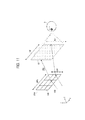
- curved portions
- optical element
- light
- Prior art date
- Legal status (The legal status is an assumption and is not a legal conclusion. Google has not performed a legal analysis and makes no representation as to the accuracy of the status listed.)
- Ceased
Links
Images

















Classifications
-
- G—PHYSICS
- G02—OPTICS
- G02B—OPTICAL ELEMENTS, SYSTEMS OR APPARATUS
- G02B5/00—Optical elements other than lenses
- G02B5/02—Diffusing elements; Afocal elements
- G02B5/0205—Diffusing elements; Afocal elements characterised by the diffusing properties
- G02B5/021—Diffusing elements; Afocal elements characterised by the diffusing properties the diffusion taking place at the element's surface, e.g. by means of surface roughening or microprismatic structures
- G02B5/0221—Diffusing elements; Afocal elements characterised by the diffusing properties the diffusion taking place at the element's surface, e.g. by means of surface roughening or microprismatic structures the surface having an irregular structure
-
- G—PHYSICS
- G02—OPTICS
- G02B—OPTICAL ELEMENTS, SYSTEMS OR APPARATUS
- G02B5/00—Optical elements other than lenses
- G02B5/02—Diffusing elements; Afocal elements
- G02B5/0205—Diffusing elements; Afocal elements characterised by the diffusing properties
- G02B5/0263—Diffusing elements; Afocal elements characterised by the diffusing properties with positional variation of the diffusing properties, e.g. gradient or patterned diffuser
-
- G—PHYSICS
- G02—OPTICS
- G02B—OPTICAL ELEMENTS, SYSTEMS OR APPARATUS
- G02B5/00—Optical elements other than lenses
- G02B5/02—Diffusing elements; Afocal elements
- G02B5/0273—Diffusing elements; Afocal elements characterized by the use
- G02B5/0278—Diffusing elements; Afocal elements characterized by the use used in transmission
Definitions
- Embodiments of the present disclosure relate to an optical element, a display device, a display system, and a mobile object.
- Display devices such as a heads-up display (HUD) are used as an application in a mobile object such as a vehicle that allows a driver (viewer) to recognize various kinds of information (for example, vehicle information, navigation information, and warning information) with a reduced amount of movement in line of vision.
- HUD heads-up display
- PTL 1 relates to a screen onto which image light is to be projected, and the screen is provided with a plurality of aperiodic lens array units in which multiple lenses are regularly and two-dimensionally arrayed. Moreover, these lenses are tightly arrayed with no gap at least within range of an image display area.
- PTL 2 relates to a screen 2 that is provided with a microlens array (MLA) 20 including an upper microlens 21H and a lower microlens 21L. Moreover, each of the microlenses has the same effective diameter (pitch diameter) and causes a difference in optical-path length ⁇ for the transmitted light.
- MVA microlens array
- An object of the present disclosure is to reduce optical noise in an optical element, a display device, a display system, and a mobile object.
- An optical element, a display device, a display system, and a mobile object is an optical element including a plurality of curved portions through which light diverges, a first irregular area including an area where a direction in which a vertex of each one of the plurality of curved portions is displaced from a virtual point of each one of the plurality of curved portions varies between a pair of the plurality of curved portions that are adjacent to each other, the virtual point being determined based on an assumption that all of the plurality of curved portions are disposed at regular intervals, and a second irregular area in which relative positions of vertices of the plurality of curved portions are equivalent to relative positions of vertices of the plurality of curved portions included in the first irregular area.
- an optical element a display device, a display system, and a mobile object that reduce optical noise can be provided.
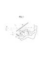
- Fig. 1 is a diagram illustrating a system configuration of a display system according to an embodiment of the present disclosure.
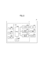
- Fig. 2 is a diagram illustrating a hardware configuration of a display device according to an embodiment of the present disclosure.
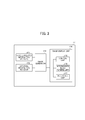
- Fig. 3 is a diagram illustrating a functional configuration of a display device according to an embodiment of the present disclosure.
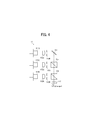
- Fig. 4 is a diagram illustrating a specific configuration of a light-source device according to an embodiment of the present disclosure.
- Fig. 1 is a diagram illustrating a system configuration of a display system according to an embodiment of the present disclosure.
- Fig. 2 is a diagram illustrating a hardware configuration of a display device according to an embodiment of the present disclosure.
- Fig. 3 is a diagram illustrating a functional configuration of a display device according to an embodiment of the present disclosure.
- Fig. 4 is a diagram illustrating a specific configuration of a light-source device according to an embodiment of the present disclosure.
- Fig. 1 is a diagram illustrating
- Fig. 5 is a diagram illustrating a specific configuration of a light deflector according to an embodiment of the present disclosure
- Fig. 6 is a diagram illustrating a specific configuration of a screen according to an embodiment of the present disclosure.
- Fig. 7A and Fig. 7B are diagrams illustrating a difference in operation due to differences in sizes of the diameter of incident light flux and the lens diameter in the microlens array, according to an embodiment of the present disclosure.
- Fig. 8 is a diagram illustrating the relation between a mirror of a light deflector and the scanning range, according to an embodiment of the present disclosure.
- Fig. 9 is a diagram illustrating the trajectory of a scanning line when two-dimensional scanning is performed, according to an embodiment of the present disclosure.
- FIG. 10 is a schematic diagram illustrating the relative positions of the elements in a display system according to an embodiment of the present disclosure.
- Fig. 11 is a diagram illustrating the relation between a microlens array and an eye box, according to an embodiment of the present disclosure.
- Fig. 12 is a diagram illustrating the relation between an intermediate image and a virtual image, according to an embodiment of the present disclosure.
- Fig. 13A and Fig. 13B are schematic diagrams each illustrating the relation between the shape of microlenses and the shape of an eye box, according to a control sample.
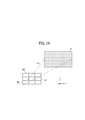
- Fig. 14 is a diagram illustrating the relation between the shape of microlenses and the shape of an eye box, according to an embodiment of the present disclosure.
- FIG. 15C are diagrams each illustrating the arrangement of microlenses in a microlens array, according to an embodiment of the present disclosure.
- Fig. 16 is a diagram illustrating the vertices of a plurality of microlenses in a random lens array, according to an embodiment of the present disclosure.
- Fig. 17 is an alternative diagram illustrating the vertices of a plurality of microlenses in a random lens array, according to an embodiment of the present disclosure.
- Fig. 18A to Fig. 18G are diagrams each illustrating an arrangement of a plurality of microlenses in a random lens array, according to an embodiment of the present disclosure.
- FIG. 19G are alternative diagrams each illustrating an arrangement of a plurality of microlenses in a random lens array, according to an embodiment of the present disclosure.
- Fig. 20A and Fig. 20B are third diagrams each illustrating an arrangement of a plurality of microlenses in a random lens array, according to an embodiment of the present disclosure.
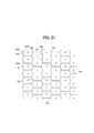
- Fig. 21 is a fourth diagram illustrating an arrangement of a plurality of microlenses in a random lens array, according to an embodiment of the present disclosure.
- Fig. 22 is a fifth diagram illustrating an arrangement of a plurality of microlenses in a random lens array, according to an embodiment of the present disclosure.
- FIG. 23C are diagrams each illustrating a concrete example of a horizontally-oriented random lens array, according to an embodiment of the present disclosure.
- Fig. 24 is a diagram illustrating the vertex of a microlens according to a control sample and the vertex of a horizontally-oriented microlens according to an embodiment of the present disclosure.
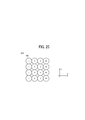
- Fig. 25 is a diagram illustrating an arrangement of a plurality of microlenses in a periodic lens array, according to an embodiment of the present disclosure.
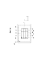
- Fig. 26 is a diagram illustrating an arrangement of a plurality of microlenses in a random lens array and a plurality of microlenses in a periodic lens array, according to an embodiment of the present disclosure.
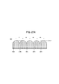
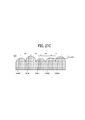
- FIG. 27C, and Fig. 27D are sectional views of periodic lens arrays and random lens arrays according to an embodiment of the present disclosure.
- Fig. 28A and Fig. 28B are diagrams each illustrating an arrangement of a plurality of microlenses in the periodic lens array 651 as illustrated in Fig. 27C.
- Fig. 29 is a diagram illustrating the images formed by the lens arrays as illustrated in Fig. 27A, Fig. 27B, and Fig. 27C.
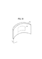
- Fig. 30 is a diagram illustrating a structure of a microlens array according to an embodiment of the present disclosure.
- Fig. 31 is a diagram illustrating a micromirror array according to an embodiment of the present disclosure.
- Fig. 1 is a diagram illustrating a system configuration of a display system according to an embodiment of the present disclosure.
- the display system 1 as illustrated in Fig. 1 can prevent the brightness of a display image from decreasing without reducing the resolution of the display image that is visually recognized by a viewer 3.
- the viewer 3 can visually identify a display image as the projection light that is projected from a display device 10 is projected onto a transmissive reflector.
- the display image is image superimposed on the viewing field of the viewer 3 as a virtual image 45.
- the display system 1 is provided for a mobile object such as a vehicle, an aircraft, and a ship, or an immobile object such as a maneuvering simulation system, and a home-theater system.
- a mobile object such as a vehicle, an aircraft, and a ship
- an immobile object such as a maneuvering simulation system
- a home-theater system cases in which the display system 1 is provided for a vehicle as an example of the mobile object is described.
- no limitation is intended thereby, and the type of usage of the display system 1 is not limited to the present embodiment.
- the display system 1 is mounted in a vehicle, and makes navigation information visible to the viewer 3 (i.e., the driver) through a front windshield 50 of the vehicle.
- the navigation information includes, for example, the information about the speed of the vehicle, the course information, the distance to a destination, the name of the current place, the presence or position of an object ahead of the vehicle, a traffic sign indicating, for example, speed limit, and traffic congestion, and aids the driving of the vehicle.
- the front windshield 50 serves as a transmissive reflector that transmits a portion of the incident light and reflects at least some of the remaining incident light.
- the distance between the location of the eyepoint of the viewer 3 and the front windshield 50 is about several tens of centimeters (cm) to one meter (m).
- the display system 1 includes a display device 10, a free-form surface mirror 30, and a front windshield 50.
- the display device 10 is a heads-up display (HUD) provided for a vehicle as an example of the mobile object.
- the display device 10 may be arranged at any desired position in conformity with the interior design of the vehicle.
- the display device 10 according to the present embodiment may be disposed under the dashboard of the vehicle or built into the dashboard of the vehicle.
- the display device 10 includes a light-source device 11, a light deflector 13, and a screen 15.
- the light-source device 11 is a device that emits the laser beams emitted from a light source outside the device.
- the light-source device 11 may emit laser beams in which three-color laser beams of red, green, and blue (RGB) are combined.
- the laser beams emitted from the light-source device 11 are guided to the reflection plane of the light deflector 13.
- the light-source device 11 has a semiconductor light-emitting element such as a laser diode (LD) that serves as a light source.
- LD laser diode
- the light source may be a semiconductor light-emitting element such as a light-emitting diode (LED).
- the light deflector 13 uses, for example, a micro-electromechanical systems (MEMS) to change the directions of travel of the laser beams.
- MEMS micro-electromechanical systems
- the light deflector 13 is configured by a scanner such as a mirror system composed of one minute MEMS mirror that pivots around two axes orthogonal to each other or two MEMS mirrors that pivot or rotates around one axis.
- the laser beams emitted from the light deflector 13 scans the screen 15.
- the light deflector 13 is not limited to a MEMS mirror, but may be configured by a polygon mirror or the like.
- the screen 15 serves as a divergent part that diverges the laser beams at a predetermined divergence angle.
- the screen 15 may consist of an exit pupil expander (EPE), and may be configured by a transmissive optical element such as a microlens array (MLA) or diffuser panel that diffuses light.
- the screen 15 may be configured by a reflective optical element such as a micromirror array that diffuses light.
- the screen 15 forms a two-dimensional intermediate image 40 on the screen 15 as the laser beams emitted from the light deflector 13 scan the surface of the screen 15.
- a method of projecting an image using the display device 10 may be implemented by a panel system or a laser scanning system.
- the intermediate image 40 is formed by an imaging device such as a liquid crystal panel, a digital micromirror device (DMD) panel (digital mirror device panel), or a vacuum fluorescent display (VFD).
- the intermediate image 40 is formed by scanning the laser beams emitted from the light-source device 11, using an optical scanner.
- the display device 10 adopts the laser scanning system.
- the laser scanning system since emitting/non-emitting can be assigned to each pixel, in general, a high-contrast image can be formed.
- the panel system may be adopted as the projection system in the display device 10.
- the virtual image 45 is projected onto the free-form surface mirror 30 and the front windshield 50 as the intermediate image 40 that is formed by the laser beams (bundle of laser beams) emitted from the screen 15 is magnified for view.
- the free-form surface mirror 30 is designed and arranged so as to cancel, for example, the inclination of the image, the distortion of the image, and the displacements of the image, which are caused by the bent shape of the front windshield 50.
- the free-form surface mirror 30 may be arranged in a pivotable manner around the rotation axis. Due to such a configuration, the free-form surface mirror 30 can adjust the reflection direction of the laser beams (bundle of laser beams) emitted from the screen 15 to change the position at which the virtual image 45 is displayed.
- the free-form surface mirror 30 is designed using a commercially available optical design simulation software such that the free-form surface mirror 30 has a certain level of light-gathering power to achieve a desired image-forming position of the virtual image 45.
- the light-gathering power of the free-form surface mirror 30 is designed such that the virtual image 45 is displayed at a position away from the location of the eyepoint of the viewer 3 in the depth direction by, for example, at least 1 m and equal to or shorter than 30 m (preferably, equal to or shorter than 10 m).
- the free-form surface mirror 30 may be a concave mirror or an element with a light-gathering power.
- the free-form surface mirror 30 is an example of an image forming optical system.
- the front windshield 50 serves as a transmissive reflector that transmits some of the laser beams (bundle of laser beams) and reflects at least some of the remaining laser beams (partial reflection).
- the front windshield 50 may serve as a semitransparent mirror through which the viewer 3 visually recognizes the virtual image 45 and the scenery ahead of the mobile object (vehicle).
- the virtual image 45 is an image that is visually recognized by the viewer 3, including vehicle-related information (e.g., speed and travel distance), navigation information (e.g., route guidance and traffic information), and warning information (e.g., collision warning).
- the transmissive reflector may be another front windshield arranged in addition to the front windshield 50.
- the front windshield 50 is an example of a reflector.
- the virtual image 45 may be displayed so as to be superimposed on the scenery ahead of the front windshield 50.
- the front windshield 50 is not flat but is curved. For this reason, the position at which the virtual image 45 is formed is determined by the curved surface of the free-form surface mirror 30 and the front windshield 50.
- the front windshield 50 may be a semitransparent mirror (combiner) that serves as a separate transmissive having a reflector partial reflection function.
- the laser beams (bundle of laser beams) emitted from the screen 15 are projected towards the free-form surface mirror 30, and are reflected by the front windshield 50. Accordingly, the viewer 3 can visually recognize the virtual image 45, i.e., the magnified image of the intermediate image 40 formed on the screen 15, due to the light reflected by the front windshield 50.
- Fig. 2 is a diagram illustrating a hardware configuration of the display device 10 according to the present embodiment. When necessary, some components or elements may be added to or deleted from the hardware configuration illustrated in Fig. 2.
- the display device 10 includes a controller 17 that controls the operation of the display device 10.
- the controller 17 is a circuit board or integrated circuit (IC) chip mounted inside the display device 10.
- the controller 17 includes a field-programmable gate array (FPGA) 1001, a central processing unit (CPU) 1002, a read only memory (ROM) 1003, a random access memory (RAM) 1004, an interface (I/F) 1005, a data bus line 1006, a laser diode (LD) driver 1008, a micro-electromechanical systems (MEMS) controller 1010, and a motor driver 1012.
- FPGA field-programmable gate array
- CPU central processing unit
- ROM read only memory
- RAM random access memory
- I/F interface
- data bus line 1006 a laser diode (LD) driver 1008, a micro-electromechanical systems (MEMS) controller 1010
- MEMS micro-electromechanical systems
- the FPGA 1001 is an integrated circuit that is configurable by the designer of the display device 10.
- the LD driver 1008, the MEMS controller 1010, and the motor driver 1012 generate a driving signal according to the control signal output from the FPGA 1001.
- the CPU 1002 is an integrated circuit that controls the entirety of the display device 10.
- the ROM 1003 is a storage device that stores a program for controlling the CPU 1002.
- the RAM 1004 is a storage device that serves as a work area of the CPU 1002.
- the interface 1005 communicates with an external device. For example, the interface 1005 is coupled to the controller area network (CAN) of a vehicle.
- CAN controller area network
- the LD 1007 is a semiconductor light-emitting element that configures a part of the light-source device 11.
- the LD driver 1008 is a circuit that generates a driving signal for driving the LD 1007.
- the MEMS 1009 configures a part of the light deflector 13 and moves the scanning mirror.
- the MEMS controller 1010 is a circuit that generates a driving signal for driving the MEMS 1009.
- the motor 1011 is an electric motor that rotates the rotation axis of the free-form surface mirror 30.
- the motor driver 1012 is a circuit that generates a driving signal for driving the motor 1011.
- Fig. 3 is a diagram illustrating a functional configuration of the display device 10 according to the present embodiment.
- the functions that are implemented by the display device 10 include a vehicle-related information receiver 171, an external information receiver 172, an image generator 173, and an image display unit 174.
- the vehicle-related information receiver 171 is a function to receive vehicle-related information (e.g., speed and travel distance) from a controller area network (CAN) or the like.
- vehicle-related information e.g., speed and travel distance
- CAN controller area network
- the vehicle-related information receiver 171 is implemented by some of the elements illustrated in Fig. 2.
- the vehicle-related information receiver 171 may be implemented by the interface 1005, the processing performed by the CPU 1002, and a program stored in the ROM 1003.
- the external information receiver 172 receives external information (for example, position information from the global positioning system (GPS), routing information from a navigation system, and traffic information) of the vehicle from an external network.
- external information for example, position information from the global positioning system (GPS), routing information from a navigation system, and traffic information
- the external information receiver 172 is implemented by some of the elements illustrated in Fig. 2.
- the external information receiver 172 may be implemented by the interface 1005, the processing performed by the CPU 1002, and a program stored in the ROM 1003.
- the image generator 173 is a function to generate image data, which is used to display the intermediate image 40 and the virtual image 45, based on the data input from the vehicle-related information receiver 171 and the external information receiver 172.
- the image generator 173 is implemented by some of the elements illustrated in Fig. 2.
- the image generator 173 may be implemented by the processing performed by the CPU 1002, and a program stored in the ROM 1003.
- the image display unit 174 is a function to form the intermediate image 40 on the screen 15 based on the image data generated by the image generator 173, and to project the laser beams (bundle of laser beams) that form the intermediate image 40 towards the front windshield 50 to display the virtual image 45.
- the image display unit 174 is implemented by some of the elements illustrated in Fig. 2.
- the image display unit 174 may be implemented by the processing performed by the CPU 1002, the FPGA 1001, the LD driver 1008, the MEMS controller 1010, and the motor driver 1012, as well as a program stored in the ROM 1003.
- the image display unit 174 includes a control unit 175, an intermediate image forming unit 176, and a projection unit 177.
- the control unit 175 In order to form the intermediate image 40, the control unit 175 generates a control signal used to control the operation of the light-source device 11 and the light deflector 13. Moreover, the control unit 175 generates a control signal that controls the operation of the free-form surface mirror 30 to display the virtual image 45 at a desired position.
- the intermediate image forming unit 176 forms the intermediate image 40 on the screen 15 based on the control signal generated by the control unit 175.
- the projection unit 177 projects the laser beams that form the intermediate image 40 towards the transmissive reflector (e.g., the front windshield 50) in order to form the virtual image 45 to be visually recognized by the viewer 3.
- Fig. 4 is a diagram illustrating a specific configuration of the light-source device 11 according to the present embodiment.
- the light-source device 11 includes light-source elements 111R, 111G, and 111B (these light-source elements may be referred to simply as a light-source element 111 in the following description when it is not necessary to distinguish each of the light-source elements), coupling lenses 112R, 112G, and 112B, apertures 113R, 113G, and 113B, combiners 114, 115, and 116, and a lens 117.
- the light-source device 11 is an example of a light source.
- each of the light-source elements 111 R, 111 G, and 111B of three colors (R, G, B) of three colors (red, green, and blue (RGB)) is a laser diode (LD) having a single or a plurality of light-emitting points.
- the light-source elements 111R, 111G, and 111B emit bundles of laser beams (light flux) having different wavelengths ⁇ R, ⁇ G, and ⁇ B, respectively.
- ⁇ R 640 nanometers (nm)
- ⁇ G 530 nm
- ⁇ B 445 nm.
- the emitted bundles of laser beams (light flux) are coupled by the coupling lenses 112R, 112G, and 112B, respectively.
- the coupled bundles of laser beams (light flux) are shaped by the apertures 113R, 113G, and 113B, respectively.
- the shape of the apertures 113R, 113G, and 113B may be various kinds of shape such as a circle, an ellipse, a rectangle, and a square depending on, for example, certain predetermined conditions such as the divergence angle of the bundles of laser beams (light flux).
- the laser beams (light flux) that are shaped by the apertures 113R, 113G, and 113B are combined by the three combiners 114, 115, and 116, respectively.
- the combiners 114, 115, and 116 are plate-like or prismatic dichroic mirrors, and reflect or transmit the laser beams (light flux) therethrough according to the wavelength of the laser beams to combine the laser beams into one bundle of laser beams (light flux) that travels along one optical path.
- the combined bundle of laser beams passes through the lens 117 and is guided to the light deflector 13.
- Fig. 5 is a diagram illustrating a specific configuration of the light deflector 13 according to the present embodiment.
- the light deflector 13 is a MEMS mirror produced by semiconductor processing, and includes a mirror 130, a serpentine beam 132, a frame 134, and a piezoelectric member 136.
- the light deflector 13 is an example of a scanner.
- the mirror 130 has a reflection plane that reflects the laser beams emitted from the light-source device 11 towards the screen 15 side.
- a pair of serpentine beams 132 are formed across the mirror 130.
- Each of the pair of serpentine beams 132 has a plurality of turning portions. Each of these turning portions is configured by a first beam 132a and a second beam 132b that are arranged alternately.
- Each of the pair of serpentine beams 132 is supported by the frame 134.
- the piezoelectric member 136 is disposed such that the first beam 132a and the second beam 132b, which are adjacent to each other, are coupled to each other.
- the piezoelectric member 136 applies different levels of voltage to the first beam 132a and the second beam 132b to bend each of the first beam 132a and the second beam 132b differently.
- the first beam 132a and the second beam 132b which are adjacent to each other, bend in different directions.
- the mirror 130 rotates in the vertical direction around the horizontal axis. Due to such a configuration as above, the light deflector 13 can perform optical scanning in the vertical direction at a low voltage.
- An optical scanning in the horizontal direction around the axis in the vertical direction is implemented by the resonance produced by a torsion bar or the like coupled to the mirror 130.
- Fig. 6 is a diagram illustrating a specific configuration of the screen 15 according to the present embodiment.
- the screen 15 serves as a divergent part that diverges the laser beams at a predetermined divergence angle.
- the screen 15 as illustrated in Fig. 6 has a microlens-array structure in which a plurality of hexagonal-shaped microlenses 150 are arranged with no gap therebetween.
- the microlenses 150 are an example of the curved portion.
- the lens diameter of each one of the microlenses 150 (the distance between two sides that are opposed to each other) is about 200 micrometers ( ⁇ m).
- the multiple microlenses 150 can be arrayed with high density.
- the microlens array 200 and the microlenses 150 according to the present embodiment will be described later in detail.
- Fig. 7A and Fig. 7B are diagrams illustrating a difference in operation due to differences in sizes of the diameter of incident light flux and the lens diameter in the microlens array 200, according to the present embodiment.
- the screen 15 is configured by an optical plate 151 in which the multiple microlenses 150 are neatly arranged.
- the incident light 152 diverges as passing through the microlenses 150, and the incident light 152 becomes a diverging light 153.
- the screen 15 can disperse the incident light 152 at a desired divergence angle 154.
- the Lens diameter 155 at which the microlenses 150 are arranged is designed to be wider than the diameter 156a of the incident light 152. Accordingly, the screen 15 does not cause interference among the lenses, and interfering noise can be prevented from occurring.
- Fig. 7B is a diagram illustrating the optical paths of diverging lights when the diameter 156b of the incident light 152 is twice wider than the lens diameter 155 at which the microlenses 150 are arranged.
- the incident light 152 is incident on two microlenses 150a and 150b, and these two microlenses 150a and 150b produce two diverging lights 157 and 158, respectively.
- lights may interfere with each other as two diverging lights exist in an area 159.
- Such an interference between two diverging lights (coherent light) is visually recognized as an interfering noise by an observer.
- the lens diameter 155 at which the microlenses 150 are arranged is designed to be wider than the diameter 156 of the incident light 152 in order to reduce the interfering noise.
- a configuration with convex lenses are described as above with reference to Fig. 7A and Fig. 7B. However, no limitation is indicated thereby, and a similar situation is expected in a configuration with concave lenses.
- Fig. 8 is a diagram illustrating the relation between the mirror 130 of the light deflector 13 and the scanning range, according to the present embodiment.
- the FPGA 1001 controls the light-emission intensity, the timing of light emission, and the light waveform of the multiple light-source elements in the light-source device 11.
- the LD driver 1008 drives the multiple light-source elements of the light-source device 11 to emit laser beams. As illustrated in Fig.
- the laser beams that are emitted from the multiple light-source elements and whose optical paths are combined are two-dimensionally deflected about the ⁇ axis and the ⁇ axis by the mirror 130 of the light deflector 13, and the screen 15 is irradiated with the laser beams deflected by the mirror 130, which serve as scanning beams.
- the screen 15 is two-dimensionally scanned by main scanning and sub-scanning by the light deflector 13.
- the entire area to be scanned by the light deflector 13 may be referred to as a scanning range.
- the scanning beams scan (two-way scans) the scanning range of the screen 15 in an oscillating manner in the main scanning direction (X-axis direction) at a high frequency of about 20,000 to 40,000 hertz (Hz), and one-way scan the scanning range of the screen 15 in the sub-scanning direction (Y-axis direction) at a low frequency of about a few tens of Hz.
- the light deflector 13 performs raster scanning on the screen 15.
- the display device 10 controls the light emission of the multiple light-source elements according to the scanning position (the position of the scanning beam). Accordingly, an image can be drawn on a pixel-by-pixel basis and a virtual image can be displayed.
- the sub-scanning cycle is about a few tens of Hz. Accordingly, the length of time to draw an image of one frame, i.e., the length of time to scan one frame (one cycle of two-dimensional scanning) is a few tens of millisecond (msec). For example, assuming that the main-scanning cycle and the sub-scanning cycle are 20,000 Hz and 50 Hz, respectively, the length of time to scan one frame is 20 msec.
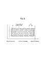
- Fig. 9 is a diagram illustrating the trajectory of a scanning line when two-dimensional scanning is performed, according to the present embodiment.
- the screen 15 includes an image area 61 (i.e., an effective scanning area) and a frame area 62 that surrounds the image area 61.
- the image area 61 is irradiated with the light that is modulated according to the image data, and the intermediate image 40 is drawn on the image area 61.
- the scanning range includes the image area 61 and a part of the frame area 62 (i.e., a portion around the periphery of the image area 61) on the screen 15.
- the trajectory of the scanning line in the scanning range is indicated by a zigzag line.
- the number of scanning lines in Fig. 9 is less than the actual number of scanning lines.
- the screen 15 may be configured by a transmissive optical element such as the microlens array 200 that diffuses light.
- the shape of the image area 61 is rectangular or planar. However, no limitation is intended thereby, and the shape of the image area 61 may be polygonal or curved.
- the screen 15 may be a reflective optical element such as a micromirror array that diffuses light, depending on the design or layout of the display device 10. In the following description of the present embodiment, it is assumed that the screen 15 is configured by the microlens array 200.
- the screen 15 is provided with a synchronous detection system 60 that includes a light receiver disposed at the edges of the image area 61 (a part of the frame area 62) in the scanning range.
- the synchronous detection system 60 is disposed on the -X and +Y side of the image area 61. More specifically, the synchronous detection system 60 is disposed at a corner on the +Y side.
- the synchronous detection system 60 detects the operation of the light deflector 13 and outputs, to the FPGA 1001, a synchronizing signal that determines the start timing of scanning or the end timing of scanning.
- a configuration of the display device 10 according to the present embodiment is described below in detail with reference to Fig. 10 to Fig. 24. Firstly, the relation between the microlenses 150 and an eye box 47 are described with reference to Fig. 10 to Fig. 14.
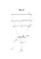
- Fig. 10 is a schematic diagram illustrating the relative positions of the elements in a display system according to the present embodiment.
- the elements of the system are arranged in parallel on the XZ plane.
- no limitation is indicated thereby, and in actuality, it is not necessary for the elements of the system to be arranged parallel to the XZ plane as illustrated in Fig. 1.
- the bundles of laser beams generated by the light-source device 11 are incident on the point a1 of the light deflector 13, and are two-dimensionally scanned on the screen 15 as deflected by the light deflector 13.
- the screen 15 forms the intermediate image 40 with a width R in the X-axis direction (main scanning direction).
- the bundles of laser beams emitted from the light-source device 11 are deflected by the light deflector 13 in the +X-direction, and a portion of the intermediate image 40 is drawn at a point b1.
- the bundles of laser beams emitted from the light-source device 11 are deflected by the light deflector 13 in the -X-direction, and a portion of the intermediate image 40 is drawn at a point c1.
- the image that is drawn on the screen 15 is configured by the image generator 173 of the controller 17.
- the screen 15 is configured by the microlens array 200.
- the bundles of laser beams that scan the screen 15 diverge at a predetermined divergence angle as passing through the microlens array 200.
- each of the laser beams that are emitted from the microlens array 200 indicates the central light beam of the diverging light.
- the bundles of laser beams that are emitted from the microlens array 200 are incident on the free-form surface mirror 30.
- Q denotes the band pass of the bundles of laser beams on the free-form surface mirror 30.
- the central light beam of the diverging light is incident on a point d1 of the free-form surface mirror 30.
- the central light beam of the diverging light is incident on a point e1 of the free-form surface mirror 30.
- the plane of the free-form surface mirror 30 is designed and shaped so as to reduce the optical strain that occurs on the front windshield 50 as.
- the bundles of laser beams that have passed through the free-form surface mirror 30 are then incident on the front windshield 50, and reach at least one point of the location of the eyepoint within an eye-lip area including the reference eyepoint of the viewer 3.
- the bundles of laser beams that are incident on the front windshield 50 are reflected according to the shape of the surface of the front windshield 50.
- the viewer 3 visually recognizes the virtual image 45 in an eye box (i.e., an area near the eyes of the viewer 3) in the optical path of the light that is reflected by the front windshield 50.
- eye box indicates the area in which the viewer 3 can visually recognize the virtual image 45 without adjusting the location of the eyepoint.
- the range of the eye box 47 is equal to or less than “the eye range of a car driver” (Japanese Industrial Standards (JIS) D 0021).
- the eye box 47 is set as the area through which the driver can visually recognize the virtual image 45, based on the eye-lip that is a region of space in which the eyepoint of the driver seated on a seat can exist.
- Fig. 11 is a diagram illustrating the relation between the microlens array 200 and the eye box 47, according to the present embodiment.
- the elements that are arranged in the optical path after the microlens array 200 are omitted in Fig. 11, and the space between the microlens array 200 and the viewer 3 is linearly expressed.
- the microlens array 200 as illustrated in Fig. 11 includes the multiple microlenses 150 that are arrayed in a two-dimensional region.
- the incident light 152 that contains the image data is incident on the multiple microlenses 150 that make up the microlens array 200.
- the viewer 3 can visually recognize a display image that includes prescribed items of information, on a region (i.e., the eye box 47) where the diverging light 153 that diverges as passing through each of the microlenses 150 can visually be recognized.
- the eye box 47 is determined by the diverging light 153 that diverges as passing through the microlens 150. Accordingly, the X-axis direction and the Y-axis direction of each of the microlenses 150 on a two-dimensional region (XY region) matches the X-axis direction and the Y-axis direction of the eye box 47.
- the aspect ratio (MX/MY) of the X-axis direction (horizontal direction) to the Y-axis direction (vertical direction) of each of the microlenses 150 is equal to the aspect ratio (AX/AY) of the X-axis direction (horizontal direction) to the Y-axis direction (vertical direction) of the eye box 47.
- the Y-axis direction (i.e., the vertical direction) of the eye box 47 is perpendicular to the line of sight of the viewer 3 such as the driver of a car.
- the X-axis direction (i.e., the horizontal direction) of the eye box 47 is in a horizontal direction perpendicular to a direction orthogonal to the line of sight of the viewer 3.
- the shape of the diverging light 153 from one of the microlenses 150 corresponds to the shape of the corresponding microlens 150.
- the shape of the microlenses 150 is to be designed according to a desired shape of the eye box 47 (visually-recognizable area).
- Fig. 12 is a diagram illustrating the relation between the intermediate image 40 and the virtual image 45, according to the present embodiment.
- the intermediate image 40 is formed as the laser beams emitted from the light deflector 13 the surface of the screen 15.
- the virtual image 45 is an image that the viewer 3 can visually identify as the projection light projected from the display device 10 is reflected by the front windshield 50.
- the intermediate image 40 that is formed on the screen 15 is magnified and projected towards the front windshield 50.
- the shape of the intermediate image 40 is similar to the shape of the virtual image 45.
- the width W and the height H of the virtual image 45 is a magnified image of the width w and the height h of the intermediate image 40.
- Fig. 13A and Fig. 13B are schematic diagrams each illustrating the relation between the shape of microlenses and the shape of an eye box, according to a control sample.
- Fig. 13A is a diagram illustrating how the incident light 152 incident on the microlenses 160a each of which is in a square shape in a planar view diverges as passing through the microlenses 160a and an eye box 46a is formed by the diverging light 153.
- the eye box 46a is square-shaped as the shape of the eye box 46a matches the shape of the microlens 160a.
- Fig. 13B is a diagram illustrating how the incident light 152 incident on the microlenses 160b each of which is a vertically-elongated rectangle in a planar view diverges as passing through the microlenses 160b and is a diagram illustrating how an eye box 46a is formed by the diverging light 153.
- the shape of the eye box 46a is a vertically oriented rectangle as the shape of the eye box 46a matches the shape of the microlens 160b.
- the display system 1 as illustrated in Fig. 1 when used as a mobile object such as a car, the X-axis direction indicates the horizontal direction and the Y-axis direction indicates the vertical direction when viewed from the driver's seat.
- the display device 10 displays, for example, a navigation image ahead of the front windshield 50 as the virtual image 45. Accordingly, the viewer 3 who is the driver can observe such a navigation image without moving his/her line of vision away from the ahead of the front windshield 50 while staying in the driver's seat.
- the front windshield 50 is horizontally oriented, and thus it is desired that the virtual image 45 be horizontally oriented when viewed from the driver.
- each of the intermediate image 40 formed on the microlenses and the virtual image 45 has a larger angle of view in the X-axis direction.
- the viewing angle be wider in the horizontal direction (X-axis direction) than in the vertical direction (Y-axis direction) such that the driver (i.e., the viewer 3) can recognize the displayed image even in a slanting direction from the right and left sides. Accordingly, a greater divergence angle (anisotropic diffusion) is required for the X-axis direction (i.e., the horizontal direction) of the virtual image 45 compared with the divergence angle (anisotropic diffusion) in the Y-axis direction (vertical direction).
- the range in the X-axis direction (i.e., the horizontal direction) of the eye box 47 needs to be configured wider than the range in the Y-axis direction (vertical direction).
- the length in the X-axis direction (i.e., the horizontal direction) of the eye boxes 46a and 46b according to the control sample as illustrated in Fig. 13A and Fig. 13B is equal to or shorter than the length in the Y-axis direction (i.e., the vertical direction) of the eye boxes 46a and 46b. Accordingly, the brightness of the image that is to be visually recognized by the viewer 3 deteriorates as the visually-recognizable area in the vertical direction needs to be expanded to secure the visually-recognizable area in the horizontal direction where the viewpoint of the driver (i.e., the viewer 3) can easily be moved.
- the microlens array 200 is arranged such that the major (longer) axis direction of the microlenses 150 matches the major (longer) axis direction of the eye box 47.
- Fig. 14 is a diagram illustrating the relation between the shape of the microlenses 150 and the shape of the eye box 47, according to the present embodiment.
- the microlenses 150 according to the present embodiment are in a horizontally-oriented shape that corresponds to the shape of the horizontally-oriented eye box 47. As illustrated in Fig.
- each of the microlenses 150 has a horizontally-oriented rectangular shape in which the sides in the X-axis direction (horizontal direction) are long and the sides in the Y-axis direction (vertical direction) are short.
- the range in the X-axis direction of the eye box 47 that is formed by the diverging light 153 that diverges as passing through the microlens 150 can be made wider than the range in the Y-axis direction to achieve a horizontally-oriented shape.
- the X-axis direction (i.e., the horizontal direction) of the microlens 150 and the eye box 47 is in the major (longer) axis direction
- the Y-axis direction (i.e., the vertical direction) is in the minor (shorter) axis direction.
- the major (longer) axis direction of the eye box 47 is in a direction orthogonal to the line of sight of the viewer 3.
- the minor (shorter) axis direction of the eye box 47 is in a horizontal direction perpendicular to a direction orthogonal to the line of sight of the viewer 3.
- the major (longer) axis direction of the microlenses 150 is the direction in which the diverging light 153 is emitted, which correspond to the range in the major (longer) axis direction of the eye box 47.
- the major (longer) axis direction of the microlenses 150 matches the major (longer) axis direction of the eye box 47 as described above, those two major (longer) axis direction (axial direction) are not necessarily parallel with each other in a strict sense. Instead, a predetermined level of utilization efficiency of light is maintained, and the range or shape of the diverging light 153 that diverges as passing through of the microlenses 150 is matched with the range or shape of the eye box 47. In other words, there may be a predetermined level of displacements in angle ranging from several degrees to several tens of degrees between the major (longer) axis direction of the microlenses 150 and the major (longer) axis of the eye box 47.
- the light diverges to a minimum area that satisfies the desired angle of view to improve the utilization efficiency of light. Due to this configuration, the brightness of the image that is to be visually recognized by the viewer 3 improves.
- the microlenses 150 are an example of a plurality of microlenses, and the microlens array 200 is an example of an optical element.
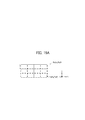
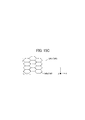
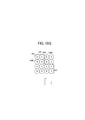
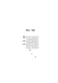
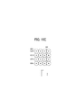
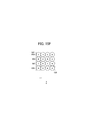
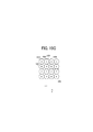
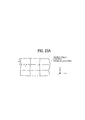
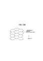
- Fig. 15A, Fig. 15B, and Fig. 15C are diagrams each illustrating the arrangement of microlenses in a microlens array, according to an embodiment of the present disclosure.
- the microlens array 200 as illustrated in Fig. 15A, Fig. 15B, and Fig. 15C is configured by the arrayed multiple microlenses 150 where the length in the X-axis direction (horizontal direction) is longer than the length in the Y-axis direction (vertical direction).
- the microlens array 200 as illustrated in Fig. 15A, Fig. 15B, and Fig. 15C is used to form the horizontally-oriented eye box 47.
- the microlens array 200a as illustrated in Fig. 15A in which the horizontally-oriented rectangular microlens 150a are arranged in a planar view is described by way of example.
- the configurations according to the present embodiment may be applied to the microlens arrays 200b and 200c as illustrated in Fig. 15B and Fig. 15C where the hexagonal microlenses 150b and 150c, which are horizontally-oriented in a planar view, are arranged, respectively.
- a horizontally-oriented hexagonal microlens 150b are densely arranged.
- the microlenses 150b do not have any side parallel to the X-axis direction (i.e., the horizontal direction).
- the upper sides and lower sides of the microlenses 150b arranged in the X-axis direction (horizontal direction) draw zigzag lines.
- the arrangement of the microlens array 200b is referred to as a zigzag-type array.
- a horizontally-oriented hexagonal microlens 152c are densely arranged.
- the microlens 150c as illustrated in Fig. 15C has a side parallel to the X-axis direction (i.e., the horizontal direction).
- the arrangement of the microlens array 200c is referred to as an armchair-type array.
- the zigzag-type array and the armchair-type array may collectively be referred to as a honeycomb-type array.
- the resolution of the image increases. Due to this configuration, preferably, the microlens array 200b or 200c in honeycomb arrangement, as illustrated in Fig. 15B or Fig. 15C, is used in the display device 10.
- the length of the microlens 150 in the X-axis direction is shorter than the pitches of lighting dots of the high-power plotted dots.
- the distance between each pair of the neighboring high-power plotted dots is shorter than the length of the microlenses 150 in the major (longer) axis direction. Due to this configuration, at least one high-power plotted dot can be formed by the multiple microlenses 150. Accordingly, in the display device 10, the variations in light intensity can be reduced on each one of the multiple microlenses 150, and the variations in brightness on the entire image can also be reduced.
- the lens diameter of the microlens 150 in the main scanning direction needs to be lengthened.
- the resolution of the image that is to be visually recognized by the viewer 3 depends on the total number of lenses of the microlens 150, and the resolution increases as the total number of microlenses is larger. Due to this configuration, in addition to the configuration in which the intensity of the light emitted from the light source is changed while the multiple microlenses 150 are being scanned, it is desired that the lens diameter in the sub-scanning direction be shorter than the lens diameter in the main scanning direction.
- the intensity of the light that is emitted from the light source can easily be changed while the multiple microlenses 150 are being scanned.
- at least one high-power plotted dot and at least one low-power plotted dot (or zero-power dots) can easily be formed on the multiple microlenses 150. Accordingly, in the display device 10, the fading rate can be increased while preventing the variations in brightness and the reduction in resolution from occurring.
- the microlens array 200 be arranged such that the main scanning direction of the light deflector 13 is matched with the major (longer) axis direction of the microlenses 150 in order to improve the utilization efficiency of light in the horizontally-oriented eye box 47.
- the pitch of the two scanning lines in the sub-scanning direction is shorter than both the lens diameter of the microlens 150 in the Y-axis direction (i.e., the minor (shorter) axis direction) and the beam diameter in the sub-scanning direction. Due to this configuration, in the display device 10, moire on the image that is to be visually recognized by the viewer 3 can be reduced to improve the image quality.
- the microlens array 200b in armchair arrangement as illustrated in Fig. 15B be used in the display device 10 in order to enhance the effect of decreasing moire.
- the shape of moire significantly changes due to a slight variation between the scanning line and the direction of the lens array. This is because, for example, the shape of moire changes from the center to periphery of the image and the viewability of the image deteriorates when the shape of the scanning line changes on the surface of the image.
- the direction of the scanning line and the vertices of lenses matches the direction of the lens array in which the vertices of lenses are connected. For this reason, the cycle of moire significantly changes due to a slight angular variation between the direction of the scanning line and the direction of the lens array, and moire easily occurs.
- the direction of the scanning line does not match the direction of the lens array in the armchair-type microlenses 150b as illustrated in Fig. 15B. In such a configuration, the shape of moire does not significantly change even if an angular variation is caused between the direction of the scanning line and the direction of the lens array, and moire does not occur.
- the lens pitch of the microlenses 150 and the randomization of the directions of the boundaries of lenses are described below with reference to Fig. 16 to Fig. 24.
- the microlens array 200 according to the present embodiment is different from known diffuser panels used to reduce the number of speckle patterns.
- a large number of bumps and dips with varying sizes are formed on the surface of a diffusing board.
- the beam spot diameter i.e., the diameter of incident light flux
- the interference between the reflected laser beams increases at such bumps and dips, and moire tends to occur.
- a random lens array where the lens diameter of each lens is equal to or greater than a prescribed value on its entirety is suggested.
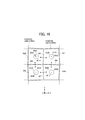
- Fig. 16 is a diagram illustrating the vertices of a plurality of microlenses in a random lens array, according to the present embodiment.
- a random lens array has structure based on a periodic lens array in which a plurality of square-shaped lenses in Fig. 16 indicated by broken lines in a grid pattern are arranged with a constant lens pitch.
- a periodic lens array is a microlens array in which the pitch (lens pitch) of the vertices of a plurality of microlenses, i.e., the spacing between the vertices of two microlenses that are adjacent to each other, is periodic (for example, constant).
- the center of each microlens is a grid point 601 (virtual point) of each tetragonal lattice when all of the multiple microlenses is disposed at regular intervals.
- the vertex of each microlens is supposed to match the grid point 601 that is the center of each microlens.
- a periodic lens array is a regular area in which a plurality of microlenses are disposed at regular intervals.
- the lens diameter of each microlens of such periodic lens arrays is set greater than the beam spot diameter (i.e., the diameter of incident light flux). In other words, the lens diameter is set to a lens diameter equal to or greater than the above prescribed value.
- a random lens array has a structure in which the vertex of each microlens of a periodic lens array is displaced (decentered) from the center within the virtual region 603 that includes the center (i.e., the grid point 601) of the microlens.
- the vertex 602 of each microlens in a random lens array is decentered.
- the vertex 602 of each microlens in a random lens array is displaced from the grid point 601 at which the microlens is arranged.
- a plurality of microlenses of a periodic lens array are individually arranged on a plurality of grid points where the lens pitch is constant, and the vertex of each microlens matches the grid point at which the microlens is arranged.
- the center of each microlens in a random lens array may be the center of the circumscribed circle (circumcircle) of the microlens, or may be the center of the inscribed circle (incircle) of the microlens.
- a random lens array is a microlens array in which the lens pitch is randomized.
- Such a random lens array has a structure in which the optical axis (Z-axis) of each microlens of a periodic lens array, where the vertex 602 of each microlens matches the center of the microlens, is randomly shifted (offset) in a direction perpendicular to the optical axis (X-axis direction, Y-axis direction).
- the lens pitch has an irregular structure in a random lens array.
- the light incident on the microlenses of the random lens array passes through the vertex 602 of each microlens, but does not pass through the center of each microlens.
- the displacement of the vertex of each one of the multiple microlenses from the center of the microlens is irregular in a random lens array, and thus the lens pitch is irregular.
- the random lens array is an irregular area in which a plurality of microlenses are disposed at irregular intervals.
- the direction in which the vertex of a microlens is displaced from the virtual point varies between a pair of neighboring microlenses.
- the line segments that connect the vertices of the arrayed microlenses 150 that are adjacent to each other in the scanning direction of the light deflector 13 are not parallel to each other in the random lens array.
- a vertex 602A in a microlens 150A is displaced within a virtual region 603A in the top-left direction with reference to a virtual point 601A as illustrated in Fig. 16, and a vertex 602B in a microlens 150B is displaced within a virtual region 603B in the bottom-left direction with reference to a virtual point 601B as illustrated in Fig. 16.
- a vertex 602C in a microlens 150C is displaced within a virtual region 603C in the bottom-right direction with reference to a virtual point 601C as illustrated in Fig. 16, and a vertex 602D in a microlens 150D is displaced within a virtual region 603D in the top-right direction with reference to a virtual point 601D as illustrated in Fig. 16.
- the directions of the boundaries of lenses of a random lens array are randomly (irregularly) displaced from the directions of the boundaries of lenses of a periodic lens array.
- the directions in which moire occurs in the multiple microlenses are different from each other.
- the directions of moire are not in line with each other macroscopically, and thus the visibility of the interfering noise decreases.
- a random lens array is not adopted, a highly coherent beam that are incident on two or more neighboring lenses is visually recognized as an interfering noise with regular cycles by an observer.
- the microlens array 200 is configured by a random lens array. Although the vertices of the lenses slightly shift in the microlens array 200, the lens diameter is approximately kept constant. Accordingly, the incident light can be prevented from sticking out from the lenses, and the interference caused by the light diverging through two of the microlenses 150 that are adjacent to each other can be reduced.
- the lens pitch is randomized in the microlens array 200, and the line segments that connect the vertices of the arrayed microlenses 150 that are adjacent to each other in the scanning direction of the light deflector 13 are not parallel to each other. Accordingly, the cycles of the interfering noise are uneven, and the interfering noise are wave-optically randomized. Due to such a configuration, the degree of interference is spread out, and the wave-optical interference-fringe noise with regular cycles is reduced. Accordingly, the visibility improves. Further, as the directions of the boundaries of lenses are randomized in the microlens array 200, the directions of the occurring interfering noise are randomized. Accordingly, the visibility of the interfering noise can significantly be reduced. Moreover, the visibility of the image (optical image) that is configured by a random lens array can be improved in the display device 10.
- the effective sectional area of the thee laser beams that are emitted from the light-source device 11 is not circular but is elliptic. Due to this configuration, as illustrated in Fig. 7A and Fig. 7B, when it is determined that the beam diameter of incident light is smaller than the lens diameter of each one of the microlenses 150, it is desired that the aspect ratio (for example, horizontally-oriented aspect ratio) be selected according to the shape (elliptical shape) of the effective sectional area of the laser beams. Accordingly, in the microlens array 200 that includes the horizontally-oriented microlenses 150, the interfering noise can be prevented from occurring with the minimum necessary lens diameter. Note that the effective sectional area indicates a portion of the cross-sectional area of the laser beams where the relative strength is between 20% and 80%.
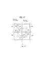
- Fig. 17 is an alternative diagram illustrating the vertices of a plurality of microlenses in a random lens array, according to the present embodiment.
- the random lens array as illustrated in Fig. 17 includes the microlenses 150A to 150C as illustrated in Fig. 16, and includes a microlens 150N in place of microlens 150D as illustrated in Fig. 16.
- a vertex 602N matches a virtual point 601N.
- the displacement between the vertex and the virtual point is directionless. Even in such a configuration, the direction in which the vertex of a microlens is displaced from the virtual point varies between a pair of neighboring microlenses.
- the distance between each pair of the vertices of neighboring microlenses does not vary to an excessive degree, and the geometrical-optical noise that is caused by the variations in the distance between each pair of the vertices of the microlenses can be reduced.
- the proportion of the microlenses 150N increases to an excessive degree, the wave-optical interference-fringe noise with regular cycles increases. For this reason, the proportion of the microlenses 150N is determined in view of the balance of the geometrical-optical noise due to a structural factor and the wave-optical interference-fringe noise with regular cycles.
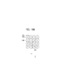
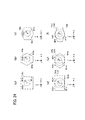
- Fig. 18A to Fig. 18G are diagrams each illustrating an arrangement of a plurality of microlenses in a random lens array, according to the present embodiment.
- the multiple microlenses 150A, 150B, 150C, and 150D as illustrated in Fig. 16 are denoted by reference signs “A,” “B,” “C,” and “D” in Fig. 18A to Fig. 18G.
- Each of the random lens arrays as illustrated in Fig. 18A and Fig. 18B includes a first irregular area 620 in which the microlens 150A and the microlens 150B are arrayed in the Y-direction and a second irregular area 630 in which the microlens 150A and the microlens 150B are similarly arrayed in the Y-direction.
- a plurality of second irregular areas 630 may be provided at different areas other than the area illustrated in the drawings.
- the direction in which each of the positions of the vertices 602A and 602B is displaced from each of the virtual points 601A and 601B is different between the adjacent microlenses 150A and 150B.
- the relative positions of the microlens 150A and the microlens 150B in the second irregular area 630 are equivalent to the relative positions of the microlens 150A and the microlens 150B in the first irregular area 620.
- the relative positions of the vertices 602A and 602B of the microlens 150A and the microlens 150B in the second irregular area 630 are equivalent to the relative positions of the vertices 602A and 602B of the microlens 150A and the microlens 150B in the first irregular area 620.
- the first irregular area 620 includes the two microlenses 150A and 150B that are arrayed in the Y-direction.
- the first irregular area 620 may include any number of microlenses and any combination of microlenses.
- the wave-optical interference-fringe noise with regular cycles is reduced as described above.
- the distance between each pair of the vertices of neighboring microlenses is remarkably long in some areas and remarkably short in other areas in a mixed manner, the geometrical-optical noise is caused by the variations in the distance between each pair of the vertices of the microlenses.
- the microlenses may be arrayed with regularity to a certain degree even in a random lens array.
- the first irregular area 620 is provided in which the direction in which each of the positions of the vertices 602A and 602B is displaced from each of the virtual points 601A and 601B is different between the adjacent microlenses 150A and 150B as illustrated in Fig. 16. Due to such a configuration, the wave-optical interference-fringe noise with regular cycles is reduced.
- the wave-optical interference-fringe noise with regular cycles is reduced in the second irregular area 630, and the distance between each pair of the vertices of microlenses does not vary to an excessive degree between the first irregular area 620 and the second irregular area 630. Due to such a configuration, in an entire area including the first irregular area 620 and the second irregular area 630, the wave-optical interference-fringe noise with regular cycles is reduced, and the geometrical-optical noise due to a structural factor is also reduced.
- Each of the random lens arrays as illustrated in Fig. 18C and Fig. 18D includes the first irregular area 620 in which the microlens 150A, the microlens 150B, and a microlens 150C are arrayed in the Y-direction and the second irregular area 630 in which the microlens 150A, the microlens 150B, and the microlens 150C are similarly arrayed in the Y-direction.
- a plurality of second irregular areas 630 may be provided at different areas other than the area illustrated in the drawings.
- the direction in which each of the positions of the vertices 602A, 602B, and 602C is displaced from each of the virtual points 601A, 601B, and 601C is different between the adjacent microlenses 150A, 150B, and 150C.
- the relative positions of the microlens 150A, the microlens 150B, and the microlens 150C in the second irregular area 630 are equivalent to the relative positions of the microlens 150A, the microlens 150B, and the microlens 150C in the first irregular area 620.
- the relative positions of the vertices 602A, 602B, and 602C of the microlens 150A, the microlens 150B, and the microlens 150C in the second irregular area 630 are equivalent to the relative positions of the vertices 602A, 602B, and 602C of the microlens 150A, the microlens 150B, and the microlens 150C in the first irregular area 620.
- the first irregular area 620 includes the three 150A, 150B, and 150C that are arrayed in the Y-direction.
- the first irregular area 620 may include any number of microlenses and any combination of microlenses.
- Each of the random lens arrays as illustrated in Fig. 18E, Fig. 18F, and Fig. 18G includes the first irregular area 620 in which the microlens 150A, the microlens 150B, the microlens 150C, and the microlens 150D are arrayed and the second irregular area 630 in which the microlens 150A, the microlens 150B, the microlens 150C, and the microlens 150D are similarly arrayed.
- a plurality of second irregular areas 630 may be provided at different areas other than the area illustrated in the drawings.
- the direction in which each of the positions of the vertices 602A, 602B, 602C, and 602D is displaced from each of the virtual points 601A, 601B, 601C, and 601D is different between the adjacent microlenses 150A, 150B, 150C, and 150D.
- the relative positions of the microlens 150A, the microlens 150B, the microlens 150C, and the microlens 150D in the second irregular area 630 are equivalent to the relative positions of the microlens 150A, the microlens 150B, the microlens 150C, and the microlens 150D in the first irregular area 620.
- the relative positions of the vertices 602A, 602B, 602C, and 602D of the microlens 150A, the microlens 150B, the microlens 150C, and the microlens 150D in the second irregular area 630 are equivalent to the relative positions of the vertices 602A, 602B, 602C, and 602D of the microlens 150A, the microlens 150B, the microlens 150C, and the microlens 150D in the first irregular area 620.
- the first irregular area 620 includes the four microlenses 150A, 150B, 150C, and 150D.
- the first irregular area 620 may include any number of microlenses and any combination of microlenses.
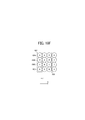
- Fig. 19A to Fig. 19G are alternative diagrams each illustrating an arrangement of a plurality of microlenses in a random lens array, according to the present embodiment.
- the multiple microlenses 150A, 150B, 150C, and 150N as illustrated in Fig. 16 are denoted by reference signs “A,” “B,” “C,” and “N” in Fig. 19A to Fig. 19G.
- Each of the random lens arrays as illustrated in Fig. 19A and Fig. 19B includes the first irregular area 620 in which the microlens 150A and the microlens 150N are arrayed in the Y-direction and the second irregular area 630 in which the microlens 150A and the microlens 150N are similarly arrayed in the Y-direction.
- a plurality of second irregular areas 630 may be provided at different areas other than the area illustrated in the drawings.
- the vertex 602N of the microlenses 150N matches the virtual point 601N.
- the displacement between the vertex and the virtual point is directionless.
- the direction in which each of the positions of the vertices 602A and 602N is displaced from each of the virtual points 601A and 601N is different between the adjacent microlenses 150A and 150N.
- the relative positions of the microlens 150A and the microlens 150N in the second irregular area 630 are equivalent to the relative positions of the microlens 150A and the microlens 150N in the first irregular area 620.
- the relative positions of the vertices 602A and 602N of the microlens 150A and the microlens 150N in the second irregular area 630 are equivalent to the relative positions of the vertices 602A and 602N of the microlens 150A and the microlens 150N in the first irregular area 620.
- the first irregular area 620 includes the two microlenses 150A and 150N that are arrayed in the Y-direction.
- the first irregular area 620 may include any number of microlenses and any combination of microlenses.
- Each of the random lens arrays as illustrated in Fig. 19C and Fig. 19D includes the first irregular area 620 in which the microlens 150A, the microlens 150B, and the microlens 150N are arrayed in the Y-direction and the second irregular area 630 in which the microlens 150A, the microlens 150B, and the microlens 150N are similarly arrayed in the Y-direction.
- a plurality of second irregular areas 630 may be provided at different areas other than the area illustrated in the drawings.
- the vertex 602N of the microlenses 150N matches the virtual point 601N.
- the displacement between the vertex and the virtual point is directionless.
- the direction in which each of the positions of the vertices 602A, 602B, and 602N is displaced from each of the virtual points 601A, 601B, and 601N is different between the adjacent microlenses 150A, 150B, and 150N.
- the relative positions of the microlens 150A, the microlens 150B, and the microlens 150N in the second irregular area 630 are equivalent to the relative positions of the microlens 150A, the microlens 150B, and the microlens 150N in the first irregular area 620.
- the relative positions of the vertices 602A, 602B, and 602N of the microlens 150A, the microlens 150B, and the microlens 150N in the second irregular area 630 are equivalent to the relative positions of the vertices 602A, 602B, and 602N of the microlens 150A, the microlens 150B, and the microlens 150N in the first irregular area 620.
- the first irregular area 620 includes the three microlenses 150A, 150B, and 150N that are arrayed in the Y-direction.
- the first irregular area 620 may include any number of microlenses and any combination of microlenses.
- Each of the random lens arrays as illustrated in Fig. 19E, Fig. 19F, and Fig. 19G includes the first irregular area 620 in which the microlens 150A, the microlens 150B, the microlens 150C, and the microlens 150N are arrayed and the second irregular area 630 in which the microlens 150A, the microlens 150B, the microlens 150C, and the microlens 150N are similarly arrayed.
- a plurality of second irregular areas 630 may be provided at different areas other than the area illustrated in the drawings.
- the vertex 602N of the microlenses 150N matches the virtual point 601N.
- the displacement between the vertex and the virtual point is directionless.
- the direction in which each of the positions of the vertices 602A, 602B, 602C and 602N is displaced from each of the virtual points 601A, 601B, 601C, and 601N is different between the adjacent microlenses 150A, 150B, 150C, and 150N.
- the relative positions of the microlens 150A, the microlens 150B, the microlens 150C, and the microlens 150N in the second irregular area 630 are equivalent to the relative positions of the microlens 150A, the microlens 150B, the microlens 150C, and the microlens 150N in the first irregular area 620.
- the relative positions of the vertices 602A, 602B, 602C, and 602N of the microlens 150A, the microlens 150B, the microlens 150C, and the microlens 150N in the second irregular area 630 are equivalent to the relative positions of the vertices 602A, 602B, 602C, and 602N of the microlens 150A, the microlens 150B, the microlens 150C, and the microlens 150N in the first irregular area 620.
- the first irregular area 620 includes the four microlenses 150A, 150B, 150C, and 150N. However, the first irregular area 620 may include any number of microlenses and any combination of microlenses.
- microlens 150N in which the vertex 602N matches the virtual point 601N is included in the random lens arrays as illustrated in Fig. 19A to Fig. 19G. Due to such a configuration, the distance between each pair of the vertices of neighboring microlenses does not vary to an excessive degree, and the geometrical-optical noise that is caused by the variations in the distance between each pair of the vertices of the microlenses can be reduced with reliability.
- the proportion of the microlenses 150N increases to an excessive degree, the wave-optical interference-fringe noise with regular cycles increases. For this reason, the proportion of the microlenses 150N is determined in view of the balance of the geometrical-optical noise due to a structural factor and the wave-optical interference-fringe noise with regular cycles.
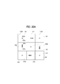
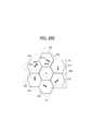
- Fig. 20A and Fig. 20B are third diagrams each illustrating an arrangement of a plurality of microlenses in a random lens array, according to the present embodiment.
- the random lens array as illustrated in Fig. 20A includes a first irregular area 620 in which a microlens 150E and the microlens 150N are arrayed, a second irregular area 631 in which a microlens 151E and the microlens 150N are arrayed, a second irregular area 632 in which a microlens 152E and the microlens 150N are arrayed, and a second irregular area 633 in which a microlens 153E and the microlens 150N are arrayed.
- a vertex 602E of the microlens 150E is displaced in the upward direction with reference to a virtual point 601E as illustrated in Fig. 20A, and the vertex 602N of the microlenses 150N matches the virtual point 601N.
- the displacement between the vertex and the virtual point is directionless. In other words, the direction in which each of the positions of the vertices 602E and 602N is displaced from each of the virtual points 601E and 601N is different between the adjacent microlenses 150E and 150N.
- the shape of the microlens 151E is equivalent to the shape of the microlenses 150E in the first irregular area 620 that is rotated in the right direction by 90 degrees
- the relative positions of the microlens 151E and the microlens 151N are equivalent to the relative positions of the microlens 150E and the microlens 150N in the first irregular area 620.
- the relative positions of the vertices of the microlens 151E and the microlens 151N in the second irregular area 631 are equivalent to the relative positions of the vertices 602E and 602N of the microlens 150E and the microlens 150N in the first irregular area 620.
- the shape of the microlens 152E is equivalent to the shape of the microlenses 150E in the first irregular area 620 that is rotated by 180 degrees, and the relative positions of the microlens 152E and the microlens 152N are equivalent to the relative positions of the microlens 150E and the microlens 150N in the first irregular area 620.
- the relative positions of the vertices of the microlens 152E and the microlens 152N in the second irregular area 632 are equivalent to the relative positions of the vertices 602E and 602N of the microlens 150E and the microlens 150N in the first irregular area 620.
- the shape of the microlens 153E is equivalent to the shape of the microlenses 150E in the first irregular area 620 that is rotated in the left direction by 90 degrees
- the relative positions of the microlens 153E and the microlens 153N are equivalent to the relative positions of the microlens 150E and the microlens 150N in the first irregular area 620.
- the relative positions of the vertices of the microlens 153E and the microlens 153N in the second irregular area 631 are equivalent to the relative positions of the vertices 602E and 602N of the microlens 150E and the microlens 150N in the first irregular area 620.
- the second irregular areas 631, 632, and 633 are rotationally symmetrical about the microlens 150N, and the vertex point matches the virtual point in the microlenses 150N that serves as the center of the rotational symmetry.
- the random lens array as illustrated in Fig. 20B includes the first irregular area 620 in which a microlens 150F and a microlens 150G are arrayed, the second irregular area 631 in which a microlens 151F and a microlens 151G are arrayed, and the second irregular area 632 in which a microlens 152F and a microlens 152G are arrayed.
- a vertex 602F of the microlens 150F is displaced in the top-right direction with reference to a virtual point 601F as illustrated in Fig. 20B
- a vertex 602G of the microlens 150G is displaced in the bottom-right direction with reference to a virtual point 601G as illustrated in Fig. 20B.
- the direction in which each of the positions of the vertices 602F and 602G is displaced from each of the virtual points 601F and 601G is different between the adjacent microlenses 150F and 150G.
- the shape of the microlens 151F is equivalent to the shape of the microlenses 150F in the first irregular area 620 that is rotated in the right direction by 120 degrees
- the shape of the microlens 151G is equivalent to the shape of the microlenses 150G in the first irregular area 620 that is rotated in the right direction by 120 degrees.
- the relative positions of the microlens 151F and the microlens 151G are equivalent to the relative positions of the microlens 150F and the microlens 150G in the first irregular area 620.
- the relative positions of the vertices of the microlens 151F and the microlens 151G in the second irregular area 631 are equivalent to the relative positions of the vertices 602F and 602G of the microlens 150F and the microlens 150G in the first irregular area 620.
- the shape of the microlens 152F is equivalent to the shape of the microlenses 150F in the first irregular area 620 that is rotated in the left direction by 120 degrees
- the shape of the microlens 152G is equivalent to the shape of the microlenses 150G in the first irregular area 620 that is rotated in the left direction by 120 degrees.
- the relative positions of the microlens 152F and the microlens 152G are equivalent to the relative positions of the microlens 150F and the microlens 150G in the first irregular area 620.
- the relative positions of the vertices of the microlens 152F and the microlens 152G in the second irregular area 632 are equivalent to the relative positions of the vertices 602F and 602G of the microlens 150F and the microlens 150G in the first irregular area 620.
- the second irregular areas 631 and 632 are rotationally symmetrical about the microlens 150N, and the vertex point matches the virtual point in the microlenses 150N that serves as the center of the rotational symmetry.
- first irregular area 620 and the second irregular areas 631 and 632 (and 633) are rotationally symmetrical about the microlens 150N in which the vertex matches the virtual point. Due to such a configuration, the distance between the vertex of the microlens 150N that serves as the rotation center and the vertex of each of the microlenses included in the first irregular area 620 and the second irregular areas 631 and 632 (and 633) does not vary to an excessive degree, and the geometrical-optical noise that is caused by the variations in the distance between each pair of the vertices of the microlenses can be reduced with reliability.
- Fig. 21 is a fourth diagram illustrating an arrangement of a plurality of microlenses in a random lens array, according to the present embodiment.
- the random lens array as illustrated in Fig. 21 includes the first irregular area 620 in which a single microlens 150H and three microlenses 150N are arrayed and second irregular areas 631 to 635 in which the single microlens 150H and the three microlenses 150N are similarly arrayed.
- a vertex 602H of the microlens 150H is displaced in the downward direction with reference to a virtual point 601H as illustrated in Fig. 21, and the vertex 602N of the three microlenses 150N matches the virtual point 601N.
- the displacement between the vertices and the virtual point is directionless.
- the direction in which each of the positions of the vertices (602H and 602N) is displaced from each of the virtual points (601H and 601N) is different between each pair of the adjacent microlenses 150H and 150N, and the first irregular area 620 includes such areas of the microlenses 150H and 150N.
- the single microlens 150H and the three microlenses 150N included in the first irregular area 620 are arrayed in a similar manner to the first irregular area 620.
- the relative positions of the microlenses included in the second irregular areas 631 to 635 are equivalent to the relative positions of the microlens 150H and the three microlenses 150N in the first irregular area 620.
- the relative positions of the vertices of the microlenses in the second irregular areas 631 to 635 are equivalent to the relative positions of the vertices of the microlens 150H and the three microlenses 150N in the first irregular area 620.
- the wave-optical interference-fringe noise with regular cycles is reduced, and the geometrical-optical noise due to a structural factor is also reduced.
- microlens 150N in which the vertex matches the virtual point is included in a similar manner to the random lens arrays as illustrated in Fig. 19A to Fig. 19G. Due to such a configuration, the distance between each pair of the vertices of neighboring microlenses does not vary to an excessive degree, and the geometrical-optical noise that is caused by the variations in the distance between each pair of the vertices of the microlenses can be reduced with reliability.
- the proportion of the microlenses 150N is determined in view of the balance of the geometrical-optical noise due to a structural factor and the wave-optical interference-fringe noise with regular cycles.
- Fig. 22 is a fifth diagram illustrating an arrangement of a plurality of microlenses in a random lens array, according to the present embodiment.
- the random lens array as illustrated in Fig. 22 includes the first irregular area 620 in which the microlenses 150J, 151J, 152J, 153J, 154J, and 155J are arrayed and second irregular areas 631 to 635.
- the vertex 602J of the microlens 150J is displaced in the left direction with reference to a virtual point 601J as illustrated in Fig. 22.
- the shape of the microlenses 151J, 152J, 153J, 154J, and 155J is equivalent to the shape of the microlenses 150J that is rotated in the right direction by 60, 120, 180, 240, and 300 degrees, respectively.
- the direction in which each of the positions of the vertices is displaced from each of the virtual points is different between each pair of the adjacent microlenses 150J, 151J, 152J, 153J, 154J, and 155J, and the first irregular area 620 includes such areas of the microlenses 150J, 151J, 152J, 153J, 154J, and 155J.
- microlenses 150J, 151J, 152J, 153J, 154J, and 155J are rotationally symmetrical about the microlens 150N, and the vertex point matches the virtual point in the microlenses 150N that serves as the center of the rotational symmetry.
- the single microlens 150N, 150J, 151J, 152J, 153J, 154J, and 155J included in the first irregular area 620 are arrayed in a similar manner to the first irregular area 620.
- the relative positions of the microlenses included in the second irregular areas 631 to 635 are equivalent to the relative positions of the microlenses 150N, 150J, 151J, 152J, 153J, 154J, and 155J in the first irregular area 620.
- the relative positions of the vertices of the microlenses in the second irregular areas 631 to 635 are equivalent to the relative positions of the vertices of the microlens 150N, 150J, 151J, 152J, 153J, 154J, and 155J in the first irregular area 620.
- each one of the first irregular area 620 and the second irregular areas 631 to 635 has a configuration similar to that of the random lens array as illustrated in Fig. 20B. Accordingly, the wave-optical interference-fringe noise with regular cycles is reduced, and the geometrical-optical noise due to a structural factor is also reduced with reliability.
- the random lens arrays as illustrated in Fig. 22 include the first irregular area 620 and the second irregular areas 631 to 635 as described above. Due to such a configuration, in the entirety of the lens arrays, the wave-optical interference-fringe noise with regular cycles is reduced, and the geometrical-optical noise due to a structural factor is reduced with reliability.
- the entirety of the microlens array 200 may be configured by the first irregular areas and the second irregular areas.
- a part of the microlens array 200 may be configured by the first irregular areas and the second irregular areas.
- the ratio of the number of the microlenses 150 included in the first irregular areas and the second irregular areas to the total number of the microlenses 150 in the entirety of the microlens array 200 is determined in view of the balance of the geometrical-optical noise due to a structural factor and the wave-optical interference-fringe noise with regular cycles. Preferably, it is desired that the ratio be equal to or greater than 50%.
- the area in the microlens array 200 from which the first irregular areas and the second irregular areas are excluded may consist of random lens arrays or periodic lens arrays.
- each one of the first irregular area 620 and the second irregular areas 631 to 635 includes the microlens 150N and the multiple microlenses 150J, 151J, 152J, 153J, 154J, and 155J that are rotationally symmetrical about the microlens 150N.
- each one of the first irregular area 620 and the second irregular areas 631 to 635 is configured by seven microlenses in total, including one microlens disposed in the center and six microlenses that are rotationally symmetrical about the microlens disposed in the center. Due to such a configuration, the wave-optical noise due to a laser beam incident on a neighboring lens can be reduced, and at the same time, the unit of repetition that is determined by the irregular areas can be minimized. Accordingly, high resolution is achieved.
- each irregular area when the irregular area increases in size, the number of intervals at which the vertices of microlenses are arranged increases, and the array has a lot of repetition including a plurality of frequency distributions. In such a configuration, the fringe noise caused by such repetition of the irregular areas is visually recognizable. In order to handle such a situation, it is desired that the size of each irregular area be smaller as much as possible. In view of such circumstances, if each irregular area includes only seven microlenses in total, including one microlens disposed in the center and six microlenses that are rotationally symmetrical about the microlens disposed in the center, the size of the irregular areas is minimized, and the loss in viewability that is caused by repetition of the irregular areas can be reduced. Furthermore, the interfering noise can be reduced.
- first irregular area 620 and the second irregular areas 631 to 635 may be configured by seven rectangular microlenses as illustrated in Fig. 15A in place of seven hexagonal microlenses in honeycomb arrangement as illustrated in Fig. 22.
- Fig. 23A, Fig. 23B, and Fig. 23C are diagrams each illustrating a concrete example of a random lens array that includes a plurality of horizontally-oriented microlenses (such a random lens array may be referred to as a horizontally-oriented random lens array in the following description), according to the present embodiment.
- the microlens array 200 according to the present embodiment that includes the horizontally-oriented microlenses 150 will be referred to as a horizontally-oriented random lens array.
- the horizontally-oriented random lens arrays as illustrated in Fig. 23A has structure based on a periodic lens array, in which a plurality of rectangular microlenses are arranged in a matrix. Each microlens of such periodic lens arrays has a horizontally oriented aspect ratio, and the relation “x>y” holds true.
- the horizontally-oriented random lens array as illustrated in Fig. 23B has structure based on a periodic lens array, in which a plurality of horizontally-oriented hexagonal microlenses are arranged in a zigzag-type array.
- the horizontally-oriented random lens array as illustrated in Fig. 23C has structure based on a periodic lens array, in which a plurality of horizontally-oriented hexagonal microlenses are arranged in an armchair-type array.
- the lens pitches and the directions of the boundaries of lenses are randomized, and thus the interfering noise with regular pitches can be prevented from occurring.
- Fig. 24 is a diagram including sub-diagrams (a) to (f), and each one of the sub-diagrams (a) to (c) illustrates the vertex of a microlens according to a control sample.
- broken lines indicate a virtual boundary, and each black-colored small square indicates the center of each microlens.
- the plus sign “+” indicates the vertex of each microlens.
- the vertex 602a of a horizontally-oriented rectangular microlens 160a is set to a random point that is selected with equal probability inside a circular virtual boundary 603a that is drawn with equal distance from the center 601a of the microlens 160a.
- the vertex 602a of the microlens 160a is randomly decentered inside the virtual boundary 603a.
- the vertex 602a of the microlens 160a can be decentralized while the maximum value for the amount of displacement from the center 601a is determined.
- the area within a virtual boundary is referred to as a decentering region.
- the microlens 160a as illustrated in Fig. 24A is horizontally oriented is not taken into consideration.
- the relative amount of random decentering in the Y-axis direction i.e., the vertical direction
- the X-direction horizontal direction
- the effects of random decentering may vary between the Y-direction (vertical direction) and the X-direction (horizontal direction).
- the effect of reduction in interfering noise increases as the random eccentricity ratio is higher.
- compressions and rarefactions occur on the lens-array surface, and structural stripes or granularity tend to increase.
- the images may appear grainy.
- the random eccentricity ratio in the Y-direction (vertical direction) and the X-direction (horizontal direction) is appropriately controlled to control the granularity.
- the random eccentricity ratio in the X-direction becomes higher than the random eccentricity ratio in the Y-direction (vertical direction).
- Fig. 24A the horizontally-oriented rectangular microlens 160a is illustrated by way of example. However, no limitation is indicated thereby, and for example, a similar configuration may be applied to the horizontally-oriented hexagonal microlens 160b and 160c illustrated in Fig. 24B and Fig. 24C, respectively.
- Fig. 24D to Fig. 24F are diagrams each illustrating the vertex of a horizontally-oriented microlens, according to the present embodiment.
- Horizontally-oriented microlenses 150a, 150b, and 150c, as illustrated in Fig. 24D, Fig. 24E, and Fig. 24F, respectively, are provided with horizontally-oriented virtual boundaries 603d, 603e, and 603f, respectively, where each of these horizontally-oriented virtual boundaries serves as a horizontally-oriented decentering region.
- the amount of random decentering in the Y-axis direction (vertical direction) and the X-axis direction (horizontal direction) can be controlled in an independent manner.
- the vertex of each microlens 150 is selected with equal probability (randomly decentered) within a horizontally-oriented decentering region. Accordingly, the sum of the amounts of decentering (i.e., the amounts of displacement from the center) in the X-axis direction at the vertices of the multiple microlenses 150 included in the horizontally-oriented random lens array is greater than the sum of the amounts of decentering (i.e., the amounts of displacement from the center) in the Y-axis direction at the vertices of the multiple microlenses 150.
- the vertex 602 (602d, 602e, and 603f) of each one of the multiple microlenses 150 are displaced from the grid points 601 (601d, 601e, 601f), and the direction in which the sum of the amounts of displacement of the vertices from the grid points is large is the major (longer) axis direction of the microlenses 150.
- the term “sum” may be replaced with “average.”
- the term “average” may be an “arithmetic mean” or “geometric mean.”
- the number of microlenses when the amount of decentering in the X-axis direction at the vertex is greater than the amount of decentering in the Y-axis direction is greater than the number of microlenses (including zero) when the amount of decentering in the Y-axis direction at the vertex is greater than the amount of decentering in the X-axis direction.
- the maximum value for the amount of decentering in the X-axis direction be less than half the value for the length of each one of the microlenses 150 in the X-axis direction, and it is desired that the maximum value for the amount of decentering in the Y-axis direction be less than half the value for the length of each one of the microlenses 150 in the X-axis direction.
- the length of a horizontally-oriented decentering region in the X-axis direction be set to, for example, a value equal to or less than four-fifth of the length of each one of the microlenses 150 in the X-axis direction
- the length of a horizontally-oriented decentering region in the Y-axis direction be set to, for example, a value equal to or less than four-fifth of the length of each one of the microlenses 150 in the Y-axis direction.
- the dimension of a horizontally-oriented decentering region may be set according to the curvature of the microlens 150 (i.e., the divergence angle). More specifically, the dimension of a horizontally-oriented decentering region may be increased as the curvature (divergence angle) of the microlenses 150 is greater.
- a horizontally-oriented decentering region does not stick out from each of the microlenses 150.
- the length of the horizontally-oriented decentering region in the X-axis direction be less than the length of each one of the microlenses 150 in the X-axis direction
- the length of the horizontally-oriented decentering region in the Y-axis direction be less than the length of that microlens 150 in the Y-axis direction.
- the dimension of a horizontally-oriented decentering region be equal to or smaller than the dimension of a regular polygon circumscribing a circle (see 604d, 604e, and 604f in Fig. 24D, Fig. 24E, and Fig. 24F, respectively) whose diameter is equal to the maximum length of the lengths of the horizontally-oriented microlenses 150 in the Y-axis direction, where the number of sides of such a regular polygon is n (where n denotes an integer equal to or greater than 3).
- the dimension of a horizontally-oriented decentering region be equal to or smaller than the dimension of the decentering region of the maximum regular polygon that can be set to the horizontally-oriented microlenses 150, where the number of sides of that regular polygon is n (where n denotes an integer equal to or greater than 3).
- the above regular polygon may be, for example, a square and a regular hexagon.
- the amount of random decentering in the vertical direction of the dimension of a horizontally-oriented decentering region can efficiently be controlled compared with the decentering region of a regular polygon whose dimension is equal to that of the horizontally-oriented decentering region, where the number of sides of that regular polygon is n (where n denotes an integer equal to or greater than 3), and thus the granularity can be prevented from increasing.
- the dimension of a horizontally-oriented decentering region be equal to or smaller than the dimension of a circle whose diameter is equal to the maximum length of the lengths of the horizontally-oriented microlenses 150 in the Y-axis direction.
- the dimension of a horizontally-oriented decentering region be equal to or smaller than the dimension of the maximum circular decentering region that can be set to a horizontally-oriented microlens.
- the dimension of a horizontally-oriented decentering region is equal to or smaller than the dimension of the decentering region of the maximum regular polygon that can be set to the horizontally-oriented microlenses 150, where the number of sides of that regular polygon is n (where n denotes an integer equal to or greater than 3).
- the aspect ratio of a horizontally-oriented decentering region is set based on the aspect ratio of the microlenses 150.
- the ratio (lx/ly) of the length lx of the horizontally-oriented decentering region in the X-axis direction to the length ly of the horizontally-oriented decentering region in the Y-axis direction is set based on the ratio (Lx/Ly) of the length Lx of the microlenses 150 in the X-axis direction to the length Ly of the microlenses 150 in the Y-axis direction.
- lx/ly is set so as to be equal to Lx/Ly.
- lx/ly may be set to be slightly greater than Lx/Ly, or may be set to be slightly less than Lx/Ly.
- the amount of random decentering in the Y-axis direction can be controlled more than the amount of random decentering in the X-axis direction, and the granularity or roughness of the surface when the surface of the microlens array 200 is visually recognized can efficiently be controlled.
- the shape of a virtual boundary may be a horizontally-oriented elliptic shape, as illustrated in Fig. 24D, Fig. 24E, and Fig. 24F.
- the shape of a virtual boundary may be a horizontally-oriented rectangular shape.
- the amount of random decentering or the degree of interference can be adjusted according to the degree of interference between diverging beams that are adjacent to each other.
- the probability distribution within a vertically-oriented decentering region may be changed or differentiated. For example, the distribution density of vertices may locally be increased or decreased within a vertically-oriented decentering region.
- Fig. 25 is a diagram illustrating an arrangement of a plurality of microlenses in a periodic lens array, according to the present embodiment.
- the microlens 150N as illustrated in Fig. 17 are denoted by the reference sign “N” in Fig. 25.
- the microlenses 150N are two-dimensionally arrayed in the XY-directions.
- the center of each one of the multiple microlenses 150 N is the grid point (virtual point) of each tetragonal lattice when all of the multiple microlenses 150N is disposed at regular intervals.
- the vertex of each of the microlenses 150N is supposed to match the grid point that is the center of each one of the microlenses 150N.
- a periodic lens array is a regular area in which a plurality of microlenses 150N are disposed at regular intervals, and the spacing between each pair of the multiple microlenses 150N can be measured with precision. Accordingly, the geometrical-optical noise that is caused by the variations in the spacing between each pair of the vertices of the multiple microlenses 150N can be reduced.
- Fig. 26 is a diagram illustrating an arrangement of a plurality of microlenses in a random lens array and a plurality of microlenses in a periodic lens array, according to the present embodiment.
- the microlens array 200 includes the random lens array (irregular areas) 640 and the periodic lens array (regular areas) 650.
- the random lens array 640 may include microlens 150A as illustrated in Fig. 16.
- the random lens array 640 may include a plurality of microlenses arrayed as illustrated in Fig. 18A to Fig. 18G or Fig. 19A to Fig. 19G, or may include a plurality of microlenses arrayed as illustrated in Fig. 20A to Fig. 22.
- the random lens array 640 may include one of or both the first irregular area 620 and the second irregular area 630.
- the periodic lens array 650 includes the microlenses 150N. More specifically, the periodic lens array 650 includes a plurality of microlenses 150N arrayed as illustrated in Fig. 25, and is disposed around the random lens array 640.
- the wave-optical interference-fringe noise with regular cycles is reduced, and the spacing between each pair of the multiple microlenses can be measured with a high degree of precision.
- the geometrical-optical noise due to a structural factor can be reduced, and the spacing between each pair of the multiple microlenses can be measured with a high degree of precision in an area around the random lens array 640.
- the image area 61 as illustrated in Fig. 9 is arranged in an area narrower than the area occupied by the random lens arrays 640, and the periodic lens array 650 is arranged outside the image area 61. Due to such a configuration, the wave-optical interference-fringe noise with regular cycles, which is caused by the periodic lens array 650, does not affect the image.
- Fig. 27A, Fig. 27B, Fig. 27C, and Fig. 27D are sectional views of periodic lens arrays and random lens arrays according to the present embodiment.
- Fig. 27A is a sectional view of the periodic lens array 650 according to the present embodiment.
- the periodic lens array 650 includes the microlenses 150N. More specifically, the periodic lens array 650 includes a plurality of microlenses 150N arrayed as illustrated in Fig. 25, and those multiple microlenses 150N are arrayed at regular intervals P1.
- Fig. 27B is a sectional view of the random lens array 620 according to the present embodiment.
- the random lens array 620 includes the microlens 150A, the microlens 150B, the microlenses 150C, and microlenses 150N as illustrated in Fig. 16, and those multiple microlenses 150N are arrayed at irregular intervals P1, P2, P3, and P4.
- the random lens array 620 may include a plurality of microlenses arrayed as illustrated in Fig. 18A to Fig. 18G or Fig. 19A to Fig. 19G, or may include a plurality of microlenses arrayed as illustrated in Fig. 20A to Fig. 22.
- Fig. 27C is a sectional view of the periodic lens array 651 according to the present embodiment.
- the periodic lens array 651 includes microlenses 150N1, 150N2, 150N3, and 150N4 that are arrayed at regular intervals P1.
- the height of the microlenses 150N1, 150N2, 150N3, and 150N4 increases in the order listed, and the height of these microlenses varies in an irregular manner.
- the microlenses 150N1, 150N2, 150N3, and 150N4 has the same curvature. In order to achieve such same curvature, the permissible range in manufacturing error needs to be small. In particular, it is desired that the difference in radius of curvature be a few micrometers ( ⁇ m). Preferably, it is desired that the difference in radius of curvature be equal to or shorter than 20 ⁇ m.
- both a microlens 150N that is reached by a light beam and another microlens 150N that is not reached by a light beam exist in a mixed manner at an edge of the image area 61. Due to such a configuration, the variations in tone tend to occur for each of the microlenses 150N. In the present embodiment, such variations in tone can be reduced.
- the height of the boundary between each pair of the microlenses 150N1, 150N2, 150N3, and 150N4 varies. In other words, the height of these boundaries varies in an irregular manner.
- Fig. 27D is a sectional view of the random lens array 621 according to the present embodiment.
- the random lens array 621 includes the microlenses 150N2 and 150N4, a microlens 150A1, a microlens 150B2, and a microlens 150C3 that are arrayed at irregular intervals P1, P2, P3, and P4.
- the height of the microlenses 150A1, 150B2, 150N2, 150C3, and 150N4 increases in the order listed, and the height of these microlenses varies in an irregular manner.
- the height of the boundary between each pair of the microlenses 150A1, 150B2, 150N2, 150C3, and 150N4 varies. In other words, the height of these boundaries varies in an irregular manner.
- Fig. 28A and Fig. 28B are diagrams each illustrating an arrangement of a plurality of microlenses in the periodic lens array 651 as illustrated in Fig. 27C, according to the present embodiment.
- a microlens 150N1 is disposed on the upper side and a microlens 150N2 is disposed on the top-right side around a central microlens 150N1 (i.e., an example of the first curved portion).
- a microlens 150N4 is disposed on the bottom-right side and the microlens 150N2 is disposed on the bottom side around the central microlens 150N1.
- the microlens 150N2 is disposed on the bottom-left side and a microlens 150N3 is disposed on the top-left side around the central microlens 150N1. Note also that these microlenses 150N1, 150N2, 150N3, and 150N4 are disposed adjacent to each other.
- the above difference in optical-path length is determined by the difference in height between the height of the microlens 150N1 and each one the microlens 150N2, and the microlens 150N3, and the microlens 150N4, and the refractive index of those microlenses for each wavelength of light.
- the difference in optical-path length with respect to the central microlens 150N1 does not match an integral multiple of the wavelengths of the light emitted from the light-source device 11 in the five microlenses including the microlens 150N2 disposed on the top-right side, the microlens 150N4 disposed on the bottom-right-right side, the microlens 150N2 disposed on the bottom side, the microlens 150N2 disposed on the bottom-left side, and the microlens 150N3 disposed on the top-left side.
- Such microlenses in which the difference in optical-path length does not match the integral multiple are an example of the first curved portion.
- the difference in optical-path length with respect to the central microlens 150N1 matches an integral multiple of the wavelength of light included in the irradiation light emitted from the light-source device 11 in one microlens that is the microlens 150N1 disposed on the upper side.
- Such microlenses in which the difference in optical-path length matches the integral multiple are an example of the second curved portion.
- the microlens 150N2 disposed on the top-right side, the microlens 150N4 disposed on the bottom-right-right side, the microlens 150N2 disposed on the bottom side, the microlens 150N2 disposed on the bottom-left side, and the microlens 150N3 disposed on the top-left side have no line symmetry and have no point symmetry around the microlens 150N1. Moreover, the optical-path lengths of the microlenses 150N2, the microlens 150N3, and the microlens 150N4 are different from each other.
- the microlens 150N2 is disposed on the upper side and the microlens 150N4 is disposed on the top-right side around the central microlens 150N1. Moreover, the microlens 150N4 is disposed on the bottom-right side and the microlens 150N4 is disposed on the bottom side around the central microlens 150N1. Further, the microlens 150N1 is disposed on the bottom-left side and the microlens 150N3 is disposed on the top-left side around the central microlens 150N1. Note also that these microlenses 150N1, 150N2, 150N3, and 150N4 are disposed adjacent to each other.
- the difference in optical-path length with respect to the central microlens 150N1 does not match an integral multiple of the wavelengths of the light emitted from the light-source device 11 in the five microlenses including the microlens 150N2 disposed on the upper side, the microlens 150N4 disposed on the top-right-side, the microlens 150N4 disposed on the bottom-right side, the microlens 150N4 disposed on the bottom side, and the microlens 150N3 disposed on the top-left side.
- Such microlenses in which the difference in optical-path length does not match the integral multiple are an example of the third curved portion.
- the difference in optical-path length with respect to the central microlens 150N1 matches an integral multiple of the wavelengths of the light emitted from the light-source device 11 in one microlens that is the microlens 150N1 disposed on the bottom-left side.
- Such microlenses in which the difference in optical-path length matches the integral multiple are an example of the fourth curved portion.
- the microlens 150N2 disposed on the top-right side, the microlens 150N4 disposed on the bottom-right-right side, the microlens 150N2 disposed on the bottom side, the microlens 150N2 disposed on the bottom-left side, and the microlens 150N3 disposed on the top-left side have no line symmetry and have no point symmetry around the microlens 150N1. Moreover, the optical-path lengths of the microlenses 150N2, the microlens 150N3, and the microlens 150N4 are different from each other.
- the relative positions of the microlenses 150N2, the microlens 150N3, and the microlens 150N4 with respect to the central microlens 150N1 in the periodic lens array 651 as illustrated in Fig. 28B are different from the relative positions of the microlenses 150N2, the microlens 150N3, and the microlens 150N4 with respect to the central microlens 150N1 in the periodic lens array 651 as illustrated in Fig. 28A.
- Fig. 29 is a diagram illustrating the images formed by the lens arrays as illustrated in Fig. 27A, Fig. 27B, and Fig. 27C, respectively, according to the present embodiment.
- Fig. 29 includes a sub-diagram (a) that illustrates an image formed by the periodic lens array 650 as illustrated in Fig. 27A.
- Fig. 29 includes a sub-diagram (b) that illustrates an image formed by the random lens array 620 as illustrated in Fig. 27B.
- Fig. 29 includes a sub-diagram (c) that illustrates an image formed by the periodic lens array 651 as illustrated in Fig. 27C.
- the lens pitch of the microlenses 150N is randomized, and the interfering noise are wave-optically randomized. Accordingly, the wave-optical interference-fringe noise with regular cycles is reduced.
- the geometrical-optical noise is caused by the variations in the distance between each pair of the vertices of the microlenses.
- the height of each one of the microlenses 150N is randomized, and the interfering noise are wave-optically randomized. Accordingly, the wave-optical interference-fringe noise with regular cycles is reduced. Further, the geometrical-optical noise is not caused by the variations in the distance between each pair of the vertices of the microlenses.
- the interference-fringe noise with regular cycles due to the difference in height of the multiple microlenses 150N and wavelength matching in the light included in the laser beams can be reduced.
- the illustration of the image that is formed by the random lens array 621 as illustrated in Fig. 27D is omitted, but such an image combines the photographic characteristics illustrated in the sub-diagram (b) of Fig. 29 with the photographic characteristics illustrated in the sub-diagram (c) of Fig. 29. More specifically, the lens pitch and height of each one of the microlenses 150N is randomized, and the interfering noise are wave-optically randomized. Accordingly, the wave-optical interference-fringe noise with regular cycles is reduced. On the other hand, the geometrical-optical noise is caused by the variations in the distance between each pair of the vertices of the microlenses. In other words, the same goes for the image as illustrated in the sub-diagram (b) of Fig. 29.
- the micro-lens array is manufactured by producing a mold having a transfer surface of a lens surface array of the micro-lens array and transferring a mold surface to a resin material by using the mold.
- the transfer surface of the mold may be formed using, for example, cutting or photolithography processes.
- the transferring of the transfer surface to the resin material can be performed, for example, by injection molding.
- the microlenses according to the present embodiment may be injection-molded with a resin material, using a mold having a transfer surface for the lens surface of a horizontally-oriented microlens.
- the wave-optical interference-fringe noise with regular cycles is reduced, and the spacing between each pair of the multiple microlenses can be measured with a high degree of precision. Moreover, the geometrical-optical noise due to variations in production can be reduced.
- the reduction of the radius of curvature of the boundary portion between the adjacent micro-lenses can be implemented by reducing the boundary width.
- the small boundary width can be implemented by "sharpening" the boundary portion formed between the adjacent micro-lens surfaces.
- the mold for micro-lens array as a method of reducing the size of the "boundary width between the adjacent micro-lenses" down to the order of wavelength, a method of increasing the radius of curvature of each micro-lens by anisotropic etching and ion processing to remove non-lens portions of the boundary portion, and a method of removing a flat surface between adjacent micro-lenses by using isotropic dry etching are known in the art.
- the above-described well-known methods it is possible to manufacture a micro-lens array where the radius of curvature of the surface constituting the boundary portion between the adjacent micro-lenses is sufficiently small.
- the above-described to-be-scanned surface can be configured as a micro-lens array having a structure where a plurality of micro-lenses are arranged to be in close contact with each other.
- the coherent noise due to the R component beam can be prevented.
- the micro-lens array where the radius of curvature r is smaller than 510 nm the coherent noise due to the R component beam and the G component beam can be prevented.
- the micro-lens array where the radius of curvature r of the surface constituting the boundary portion between the adjacent micro-lenses is smaller than 445 nm, the coherent noise due to the R, G, and B component beams can be prevented.
- the microlens array 200 may be curved in the entire array structure.
- the direction of curvature (X-axis direction) of the microlens array 200 is matched with the major (longer) axis direction (X-axis direction) of the microlenses 150. Due to this configuration, in the display device 10, the divergence angle of the diverging light 153 that diverges as passing through the microlenses 150 can be adjusted to a desired angle of view without being affected by the size of the microlens array 200, and the utilization efficiency of light improves.
- the difference in optical-path length between the optical scanning element (i.e., a MEMS mirror) and lens-array surface can be Kept constant in the display device 10.
- the beam diameter formed on the lens-array surface is determined by the optical-path length, the beam diameter can be kept constant in the display device 10 when the lens-array surface is curved.
- the beam diameter can be kept constant in the display device 10. As a result, the interfering noise can be reduced, and high resolution is achieved.
- a micromirror array (a micro convex mirror structure as an example of a curved portion, in other words, an optical element having a plurality of projections arranged in an array) may be employed as the to-be-scanned surface.
- the embodiments as described above can be practiced with a micromirror array instead of a microlens array.
- a micromirror may be a concave portion. In such a configuration, the vertex of such a concave portion corresponds to the vertex of a convex portion that has a similar figure to that concave portion.
- Fig. 31 is a diagram illustrating a micromirror array (MMA) 3000 as an optical element having a micro-convex mirror arrangement, according to the present embodiment.
- MMA micromirror array
- the micromirror array 3000 is provided with a plurality of micro convex mirrors (micromirrors) 3001 arranged in an array.
- the size 3001a of the micro convex mirror 3001 is larger than the diameter 156a of the incident light 152.
- the incident light 152 according to the present embodiment is light flux and has a light intensity distribution of a Gaussian distribution around the center of the light flux. Accordingly, the diameter 156a indicates the distance in the radial direction of light flux, where the light intensity in the light intensity distribution is decreased to “1/e2.”
- the diameter 156a is illustrated to have a size equal to the size 3001a of the micro convex mirror 3001. However, the diameter 156a does not need to be equal to the size 3001a of the micro convex mirror 3001. The point is that the incident light beam to the micro convex mirror 3001 only has to be within the micro convex mirror 3001.
- the entire incident light 152 is incident on a single micro convex mirror 3001, and is converted into diffused light flux 3004 with a divergence angle 3005.
- the “divergence angle” may be referred to as a “diffusion angle” in some cases.
- Fig. 31 no coherent noise (speckle noise) occurs as the diffused light flux 3004 does not interfere with any light flux.
- the size of the divergence angle 3005 may be set by adjusting the shape of the micro convex mirror 3001 as appropriate.
- the optical element is the optical element 200 or the optical element 15 provided with a plurality of microlenses 150 or micro convex mirrors (micromirrors) 3001, which is an example of a curved portion through which the light diverges.
- microlenses 150 or micro convex mirrors (micromirrors) 3001 which is an example of a curved portion through which the light diverges.
- the optical element includes the first irregular area 620 that includes an area in which the direction in which the vertex 602 of a curved portion is displaced from the virtual point 601 varies between a pair of neighboring curved portions, and the second irregular area 630 in which the relative positions of the vertices of a plurality of curved portions are equivalent to the relative positions of the vertices of a plurality of curved portions included in the first irregular area 620.
- the wave-optical interference-fringe noise with regular cycles is reduced in the first irregular area 620, and the wave-optical interference-fringe noise with regular cycles is also reduced in the second irregular area 630 in which the relative positions of the vertices of the curved portions are equivalent to the relative positions of the vertices of the curved portions included in the first irregular area 620.
- the distance between each pair of the vertices of curved portions does not vary to an excessive degree between the first irregular area 620 and the second irregular area 630. Due to such a configuration, in an entire area including the first irregular area 620 and the second irregular area 630, the wave-optical interference-fringe noise with regular cycles is reduced, and the geometrical-optical noise due to a structural factor is also reduced.
- the first irregular area 620 includes a curved portion in which the vertex 602N matches the virtual point 601N. Due to such a configuration, the distance between each pair of the vertices of neighboring curved portions does not vary to an excessive degree, and the geometrical-optical noise that is caused by the variations in the distance between each pair of the vertices of the curved portions can be reduced with reliability.
- the second irregular area 631 is disposed in a rotationally symmetrical manner.
- a curved portion in which the vertex 602N matches the virtual point 601N is arranged in the center of rotational symmetry between the first irregular area 620 and the second irregular area 631.
- the distance between the vertex of the curved portion that serves as the center of rotational symmetry and the vertex of each of the curved portions included in the first irregular area 620 and the second irregular area 631 does not vary to an excessive degree, and the geometrical-optical noise that is caused by the variations in the distance between each pair of the vertices of the curved portions can be reduced with reliability.
- the optical element is the optical element 200 or the optical element 15 provided with a plurality of microlenses 150 or micro convex mirrors (micromirrors) 3001, which is an example of a curved portion through which the light diverges, and includes the irregular area 640 in which a plurality of curved portions are disposed at irregular intervals and the regular area 650 in which a plurality of curved portions are disposed at regular intervals.
- the irregular area 640 includes an area in which the direction in which the vertex 602 of a curved portion is displaced from the virtual point 601 varies between a pair of neighboring curved portions, and the vertex of the curved portion matches the virtual point in the regular area 650.
- the wave-optical interference-fringe noise with regular cycles is reduced, and the spacing between each pair of the multiple curved portions can be measured with a high degree of precision.
- the geometrical-optical noise due to a structural factor can be reduced, and
- the regular area 650 is arranged outside the image area 61 on which an image is formed. Due to such a configuration, the wave-optical interference-fringe noise with regular cycles due to the regular area 650 does not affect the image.
- the regular area 650 is disposed around the irregular area 640 (the first irregular area 620 and the second irregular area 630). Due to such a configuration, in an area around the irregular area 640, the spacing between each pair of the multiple microlenses can be measured with a high degree of precision, and the geometrical-optical noise due to a structural factor can be reduced.
- the optical element is the optical element 200 or the optical element 15 provided with a plurality of microlenses 150 or micro convex mirrors (micromirrors) 3001, which is an example of a curved portion through which the light emitted from light-source device 11 diverges.
- the wave-optical interference-fringe noise with regular cycles which is caused by phenomenon in which the difference in optical-path length between the one particular curved portion and its neighboring curved portions matches an integral multiple of the wavelength of light included in the irradiation light, can be reduced.
- the first curved portions are not symmetrical about the one particular curved portion.
- the number of third curved portions in which the difference in optical-path length with that another particular curved portion does not match an integral multiple of the wavelengths of the irradiation light is greater than the number of fourth curved portions in which the difference in optical-path length with that another particular curved portion matches an integral multiple of the wavelengths of the irradiation light, and the position of the third curved portion with respect to that another particular curved portion is different from the position of the first curved portion with respect to that one particular curved portion. Due to such a configuration, the wave-optical interference-fringe noise with regular cycles can further be reduced.
- the first curved portion may include a plurality of curved portions whose optical-path lengths are different from each other.
- those multiple curved portions each of which has different height are arrayed at regular intervals. Due to such a configuration, the geometrical-optical noise that is caused by the variations in the distance between each pair of the vertices of the curved portions be reduced.
- a display device is the display device 10 that includes the optical element 200 or the optical element 15 provided with a plurality of microlenses 150 or micro convex mirrors (micromirrors) 3001, which is an example of a curved portion through which the light diverges, and forms an image by projecting the laser beam diverging through the optical element 200 or the optical element 15.
- microlenses 150 or micro convex mirrors 3001 which is an example of a curved portion through which the light diverges, and forms an image by projecting the laser beam diverging through the optical element 200 or the optical element 15.
- the optical element 200 or the optical element 15 includes the first irregular area 620 that includes an area in which the direction in which the vertex 602 of a curved portion is displaced from the virtual point 601 varies between a pair of curved portions, and the second irregular area 630 in which the relative positions of the vertices of a plurality of curved portions are equivalent to the relative positions of the vertices of a plurality of curved portions included in the first irregular area 620.
- the display device 10 can be provided in which Due to such a configuration, the wave-optical interference-fringe noise with regular cycles is reduced, the geometrical-optical noise due to a structural factor is reduced, and the viewability improves.
- a display device is the display device 10 that includes the optical element 200 or the optical element 15 provided with a plurality of microlenses 150 or micro convex mirrors (micromirrors) 3001, which is an example of a curved portion through which the light diverges, and forms an image by projecting the laser beam diverging through the optical element 200 or the optical element 15.
- the optical element 200 or the optical element 15 includes the irregular area 640 in which a plurality of curved portions are disposed at irregular intervals and the regular area 650 in which a plurality of curved portions are disposed at regular intervals.
- the display device 10 can be provided in which the wave-optical interference-fringe noise with regular cycles is reduced, the spacing between each pair of the multiple curved portions can be measured with a high degree of precision, and the geometrical-optical noise due to a structural factor can be reduced.
- a display device is the display device 10 that includes the optical element 200 or the optical element 15 provided with a plurality of microlenses 150 or micro convex mirrors (micromirrors) 3001, which is an example of a curved portion through which the light emitted from the light-source device 11 diverges, and forms an image by projecting the laser beam diverging through the optical element 200 or the optical element 15.
- microlenses 150 or micro convex mirrors 3001 micro convex mirrors
- the wave-optical interference-fringe noise with regular cycles which is caused by phenomenon in which the difference in optical-path length between the one particular curved portion and its neighboring curved portions matches an integral multiple of the wavelength of light included in the irradiation light, can be reduced.
- each one of the microlenses 150 or micro convex mirrors (micromirrors) 3001 which is an example of a curved portions through which the light diverges, is two-dimensionally scanned by main scanning and sub-scanning by the light deflector 13 (an example of a scanner), and is arranged such that the main-scanning direction matches the major (longer) axis direction of the curved portion. Due to this configuration, in the display device 10, the longer axis direction of the curved portion matches the main scanning direction of the light deflector 13, and the extinction ratio in the image that is to be visually recognized by the viewer 3 can be improved.
- the display system 1 is provided with the display device 10, the front windshield 50 (an example of a reflector) that reflects the diverging light 153 diverging through the optical element 200 or the optical element 15, and the free-form surface mirror 30 (an example of an imaging optical system) that projects the diverging light diverging 153 from the optical element 200 or the optical element 15 towards the front windshield 50 to form the virtual image 45. Due to such a configuration, in the display system 1, the viewability of the image that is to be visually recognized by the viewer 3 can be improved.
- the display device is applicable not only to a heads-up display (HUD) but also to, for example, a head-mounted display, a prompter, and a projector.
- a display device when a display device according to an embodiment of the present disclosure is applied to a projection device, such a projection device can be configured in a similar manner to the display device 10.
- the display device 10 may project the image light onto, for example, a projection screen or a wall through the free-form surface mirror 30.
- the display device 10 may project the image light that has passed through the screen 15 onto, for example, a projection screen or a wall, without involving the free-form surface mirror 30.
- Display system 10 Display device 11
- Light-source device an example of a light source
- Light deflector 15
- Screen 30
- Free-form surface mirror 45
- Eye box (an example of a visually-recognizable area)
- Front windshield an example of a reflector)
- Microlens an example of a curved portion or a curved surface
- Microlens array an example of an optical element
- 620 621
- First irregular area 630
- Second irregular area 640 Irregular area (random lens array) 650, 651 Regular area (periodic lens array)
- Micromirror array an example of an optical element
Landscapes
- Physics & Mathematics (AREA)
- General Physics & Mathematics (AREA)
- Optics & Photonics (AREA)
- Instrument Panels (AREA)
Abstract
An optical element includes a plurality of curved portions through which light diverges, a first irregular area including an area where a direction in which a vertex of each one of the plurality of curved portions is displaced from a virtual point of each one of the plurality of curved portions varies between a pair of the plurality of curved portions that are adjacent to each other, the virtual point being determined based on an assumption that all of the plurality of curved portions are disposed at regular intervals, and a second irregular area in which relative positions of vertices of the plurality of curved portions are equivalent to relative positions of vertices of the plurality of curved portions included in the first irregular area.
Description
Embodiments of the present disclosure relate to an optical element, a display device, a display system, and a mobile object.
Display devices such as a heads-up display (HUD) are used as an application in a mobile object such as a vehicle that allows a driver (viewer) to recognize various kinds of information (for example, vehicle information, navigation information, and warning information) with a reduced amount of movement in line of vision.
An object of the present disclosure is to reduce optical noise in an optical element, a display device, a display system, and a mobile object.
An optical element, a display device, a display system, and a mobile object according to the present disclosure is an optical element including a plurality of curved portions through which light diverges, a first irregular area including an area where a direction in which a vertex of each one of the plurality of curved portions is displaced from a virtual point of each one of the plurality of curved portions varies between a pair of the plurality of curved portions that are adjacent to each other, the virtual point being determined based on an assumption that all of the plurality of curved portions are disposed at regular intervals, and a second irregular area in which relative positions of vertices of the plurality of curved portions are equivalent to relative positions of vertices of the plurality of curved portions included in the first irregular area.
According to one aspect of the present disclosure, an optical element, a display device, a display system, and a mobile object that reduce optical noise can be provided.
The accompanying drawings are intended to depict example embodiments of the present invention and should not be interpreted to limit the scope thereof. The accompanying drawings are not to be considered as drawn to scale unless explicitly noted. Also, identical or similar reference numerals designate identical or similar components throughout the several views.
Fig. 1 is a diagram illustrating a system configuration of a display system according to an embodiment of the present disclosure.
Fig. 2 is a diagram illustrating a hardware configuration of a display device according to an embodiment of the present disclosure.
Fig. 3 is a diagram illustrating a functional configuration of a display device according to an embodiment of the present disclosure.
Fig. 4 is a diagram illustrating a specific configuration of a light-source device according to an embodiment of the present disclosure.
Fig. 5 is a diagram illustrating a specific configuration of a light deflector according to an embodiment of the present disclosure
Fig. 6 is a diagram illustrating a specific configuration of a screen according to an embodiment of the present disclosure.
Fig. 7A and Fig. 7B are diagrams illustrating a difference in operation due to differences in sizes of the diameter of incident light flux and the lens diameter in the microlens array, according to an embodiment of the present disclosure.
Fig. 8 is a diagram illustrating the relation between a mirror of a light deflector and the scanning range, according to an embodiment of the present disclosure.
Fig. 9 is a diagram illustrating the trajectory of a scanning line when two-dimensional scanning is performed, according to an embodiment of the present disclosure.
Fig. 10 is a schematic diagram illustrating the relative positions of the elements in a display system according to an embodiment of the present disclosure.
Fig. 11 is a diagram illustrating the relation between a microlens array and an eye box, according to an embodiment of the present disclosure.
Fig. 12 is a diagram illustrating the relation between an intermediate image and a virtual image, according to an embodiment of the present disclosure.
Fig. 13A and Fig. 13B are schematic diagrams each illustrating the relation between the shape of microlenses and the shape of an eye box, according to a control sample.
Fig. 14 is a diagram illustrating the relation between the shape of microlenses and the shape of an eye box, according to an embodiment of the present disclosure.
Fig. 15A, Fig. 15B, and Fig. 15C are diagrams each illustrating the arrangement of microlenses in a microlens array, according to an embodiment of the present disclosure.
Fig. 16 is a diagram illustrating the vertices of a plurality of microlenses in a random lens array, according to an embodiment of the present disclosure.
Fig. 17 is an alternative diagram illustrating the vertices of a plurality of microlenses in a random lens array, according to an embodiment of the present disclosure.
Fig. 18A to Fig. 18G are diagrams each illustrating an arrangement of a plurality of microlenses in a random lens array, according to an embodiment of the present disclosure.
Fig. 19A to Fig. 19G are alternative diagrams each illustrating an arrangement of a plurality of microlenses in a random lens array, according to an embodiment of the present disclosure.
Fig. 20A and Fig. 20B are third diagrams each illustrating an arrangement of a plurality of microlenses in a random lens array, according to an embodiment of the present disclosure.
Fig. 21 is a fourth diagram illustrating an arrangement of a plurality of microlenses in a random lens array, according to an embodiment of the present disclosure.
Fig. 22 is a fifth diagram illustrating an arrangement of a plurality of microlenses in a random lens array, according to an embodiment of the present disclosure.
Fig. 23A, Fig. 23B, and Fig. 23C are diagrams each illustrating a concrete example of a horizontally-oriented random lens array, according to an embodiment of the present disclosure.
Fig. 24 is a diagram illustrating the vertex of a microlens according to a control sample and the vertex of a horizontally-oriented microlens according to an embodiment of the present disclosure.
Fig. 25 is a diagram illustrating an arrangement of a plurality of microlenses in a periodic lens array, according to an embodiment of the present disclosure.
Fig. 26 is a diagram illustrating an arrangement of a plurality of microlenses in a random lens array and a plurality of microlenses in a periodic lens array, according to an embodiment of the present disclosure.
Fig. 27A, Fig. 27B, Fig. 27C, and Fig. 27D are sectional views of periodic lens arrays and random lens arrays according to an embodiment of the present disclosure.
Fig. 28A and Fig. 28B are diagrams each illustrating an arrangement of a plurality of microlenses in the periodic lens array 651 as illustrated in Fig. 27C.
Fig. 29 is a diagram illustrating the images formed by the lens arrays as illustrated in Fig. 27A, Fig. 27B, and Fig. 27C.
Fig. 30 is a diagram illustrating a structure of a microlens array according to an embodiment of the present disclosure.
Fig. 31 is a diagram illustrating a micromirror array according to an embodiment of the present disclosure.
Embodiments of the present disclosure are described below with reference to the accompanying drawings. In the description of the drawings, like reference signs denote like elements, and overlapping descriptions are omitted.
Embodiments
Fig. 1 is a diagram illustrating a system configuration of a display system according to an embodiment of the present disclosure. The display system 1 as illustrated in Fig. 1 can prevent the brightness of a display image from decreasing without reducing the resolution of the display image that is visually recognized by a viewer 3.
In the display system 1, the viewer 3 can visually identify a display image as the projection light that is projected from a display device 10 is projected onto a transmissive reflector. The display image is image superimposed on the viewing field of the viewer 3 as a virtual image 45. For example, the display system 1 is provided for a mobile object such as a vehicle, an aircraft, and a ship, or an immobile object such as a maneuvering simulation system, and a home-theater system. In the present embodiment, cases in which the display system 1 is provided for a vehicle as an example of the mobile object is described. However, no limitation is intended thereby, and the type of usage of the display system 1 is not limited to the present embodiment.
For example, the display system 1 is mounted in a vehicle, and makes navigation information visible to the viewer 3 (i.e., the driver) through a front windshield 50 of the vehicle. The navigation information includes, for example, the information about the speed of the vehicle, the course information, the distance to a destination, the name of the current place, the presence or position of an object ahead of the vehicle, a traffic sign indicating, for example, speed limit, and traffic congestion, and aids the driving of the vehicle. In such cases, the front windshield 50 serves as a transmissive reflector that transmits a portion of the incident light and reflects at least some of the remaining incident light. The distance between the location of the eyepoint of the viewer 3 and the front windshield 50 is about several tens of centimeters (cm) to one meter (m).
The display system 1 includes a display device 10, a free-form surface mirror 30, and a front windshield 50. For example, the display device 10, is a heads-up display (HUD) provided for a vehicle as an example of the mobile object. The display device 10 may be arranged at any desired position in conformity with the interior design of the vehicle. For example, the display device 10 according to the present embodiment may be disposed under the dashboard of the vehicle or built into the dashboard of the vehicle.
The display device 10 includes a light-source device 11, a light deflector 13, and a screen 15. The light-source device 11 is a device that emits the laser beams emitted from a light source outside the device. For example, the light-source device 11 may emit laser beams in which three-color laser beams of red, green, and blue (RGB) are combined. The laser beams emitted from the light-source device 11 are guided to the reflection plane of the light deflector 13. For example, the light-source device 11 has a semiconductor light-emitting element such as a laser diode (LD) that serves as a light source. However, no limitation is intended thereby, and the light source may be a semiconductor light-emitting element such as a light-emitting diode (LED).
The light deflector 13 uses, for example, a micro-electromechanical systems (MEMS) to change the directions of travel of the laser beams. For example, the light deflector 13 is configured by a scanner such as a mirror system composed of one minute MEMS mirror that pivots around two axes orthogonal to each other or two MEMS mirrors that pivot or rotates around one axis. The laser beams emitted from the light deflector 13 scans the screen 15. The light deflector 13 is not limited to a MEMS mirror, but may be configured by a polygon mirror or the like.
The screen 15 serves as a divergent part that diverges the laser beams at a predetermined divergence angle. For example, the screen 15 may consist of an exit pupil expander (EPE), and may be configured by a transmissive optical element such as a microlens array (MLA) or diffuser panel that diffuses light. Alternatively, the screen 15 may be configured by a reflective optical element such as a micromirror array that diffuses light. The screen 15 forms a two-dimensional intermediate image 40 on the screen 15 as the laser beams emitted from the light deflector 13 scan the surface of the screen 15.
A method of projecting an image using the display device 10 may be implemented by a panel system or a laser scanning system. In the panel system, the intermediate image 40 is formed by an imaging device such as a liquid crystal panel, a digital micromirror device (DMD) panel (digital mirror device panel), or a vacuum fluorescent display (VFD). In the laser scanning system, the intermediate image 40 is formed by scanning the laser beams emitted from the light-source device 11, using an optical scanner.
The display device 10 according to the present embodiment adopts the laser scanning system. In particular, in the laser scanning system, since emitting/non-emitting can be assigned to each pixel, in general, a high-contrast image can be formed. In some alternative embodiments, the panel system may be adopted as the projection system in the display device 10.
The virtual image 45 is projected onto the free-form surface mirror 30 and the front windshield 50 as the intermediate image 40 that is formed by the laser beams (bundle of laser beams) emitted from the screen 15 is magnified for view. The free-form surface mirror 30 is designed and arranged so as to cancel, for example, the inclination of the image, the distortion of the image, and the displacements of the image, which are caused by the bent shape of the front windshield 50. The free-form surface mirror 30 may be arranged in a pivotable manner around the rotation axis. Due to such a configuration, the free-form surface mirror 30 can adjust the reflection direction of the laser beams (bundle of laser beams) emitted from the screen 15 to change the position at which the virtual image 45 is displayed.
In the present embodiment, the free-form surface mirror 30 is designed using a commercially available optical design simulation software such that the free-form surface mirror 30 has a certain level of light-gathering power to achieve a desired image-forming position of the virtual image 45. In the display device 10, the light-gathering power of the free-form surface mirror 30 is designed such that the virtual image 45 is displayed at a position away from the location of the eyepoint of the viewer 3 in the depth direction by, for example, at least 1 m and equal to or shorter than 30 m (preferably, equal to or shorter than 10 m). The free-form surface mirror 30 may be a concave mirror or an element with a light-gathering power. The free-form surface mirror 30 is an example of an image forming optical system.
The front windshield 50 serves as a transmissive reflector that transmits some of the laser beams (bundle of laser beams) and reflects at least some of the remaining laser beams (partial reflection). The front windshield 50 may serve as a semitransparent mirror through which the viewer 3 visually recognizes the virtual image 45 and the scenery ahead of the mobile object (vehicle). The virtual image 45 is an image that is visually recognized by the viewer 3, including vehicle-related information (e.g., speed and travel distance), navigation information (e.g., route guidance and traffic information), and warning information (e.g., collision warning). For example, the transmissive reflector may be another front windshield arranged in addition to the front windshield 50.
Thefront windshield 50 is an example of a reflector.
The
The virtual image 45 may be displayed so as to be superimposed on the scenery ahead of the front windshield 50. The front windshield 50 is not flat but is curved. For this reason, the position at which the virtual image 45 is formed is determined by the curved surface of the free-form surface mirror 30 and the front windshield 50. In some embodiments, the front windshield 50 may be a semitransparent mirror (combiner) that serves as a separate transmissive having a reflector partial reflection function.
Due to such a configuration as above, the laser beams (bundle of laser beams) emitted from the screen 15 are projected towards the free-form surface mirror 30, and are reflected by the front windshield 50. Accordingly, the viewer 3 can visually recognize the virtual image 45, i.e., the magnified image of the intermediate image 40 formed on the screen 15, due to the light reflected by the front windshield 50.
Fig. 2 is a diagram illustrating a hardware configuration of the display device 10 according to the present embodiment. When necessary, some components or elements may be added to or deleted from the hardware configuration illustrated in Fig. 2.
The display device 10 includes a controller 17 that controls the operation of the display device 10. For example, the controller 17 is a circuit board or integrated circuit (IC) chip mounted inside the display device 10. The controller 17 includes a field-programmable gate array (FPGA) 1001, a central processing unit (CPU) 1002, a read only memory (ROM) 1003, a random access memory (RAM) 1004, an interface (I/F) 1005, a data bus line 1006, a laser diode (LD) driver 1008, a micro-electromechanical systems (MEMS) controller 1010, and a motor driver 1012.
The FPGA 1001 is an integrated circuit that is configurable by the designer of the display device 10. The LD driver 1008, the MEMS controller 1010, and the motor driver 1012 generate a driving signal according to the control signal output from the FPGA 1001. The CPU 1002 is an integrated circuit that controls the entirety of the display device 10. The ROM 1003 is a storage device that stores a program for controlling the CPU 1002. The RAM 1004 is a storage device that serves as a work area of the CPU 1002. The interface 1005 communicates with an external device. For example, the interface 1005 is coupled to the controller area network (CAN) of a vehicle.
For example, the LD 1007 is a semiconductor light-emitting element that configures a part of the light-source device 11. The LD driver 1008 is a circuit that generates a driving signal for driving the LD 1007. The MEMS 1009 configures a part of the light deflector 13 and moves the scanning mirror. The MEMS controller 1010 is a circuit that generates a driving signal for driving the MEMS 1009. The motor 1011 is an electric motor that rotates the rotation axis of the free-form surface mirror 30. The motor driver 1012 is a circuit that generates a driving signal for driving the motor 1011.
Fig. 3 is a diagram illustrating a functional configuration of the display device 10 according to the present embodiment. The functions that are implemented by the display device 10 include a vehicle-related information receiver 171, an external information receiver 172, an image generator 173, and an image display unit 174.
The vehicle-related information receiver 171 is a function to receive vehicle-related information (e.g., speed and travel distance) from a controller area network (CAN) or the like. For example, the vehicle-related information receiver 171 is implemented by some of the elements illustrated in Fig. 2. In particular, the vehicle-related information receiver 171 may be implemented by the interface 1005, the processing performed by the CPU 1002, and a program stored in the ROM 1003.
The external information receiver 172 receives external information (for example, position information from the global positioning system (GPS), routing information from a navigation system, and traffic information) of the vehicle from an external network. For example, the external information receiver 172 is implemented by some of the elements illustrated in Fig. 2. In particular, the external information receiver 172 may be implemented by the interface 1005, the processing performed by the CPU 1002, and a program stored in the ROM 1003.
The image generator 173 is a function to generate image data, which is used to display the intermediate image 40 and the virtual image 45, based on the data input from the vehicle-related information receiver 171 and the external information receiver 172. For example, the image generator 173 is implemented by some of the elements illustrated in Fig. 2. In particular, the image generator 173 may be implemented by the processing performed by the CPU 1002, and a program stored in the ROM 1003.
The image display unit 174 is a function to form the intermediate image 40 on the screen 15 based on the image data generated by the image generator 173, and to project the laser beams (bundle of laser beams) that form the intermediate image 40 towards the front windshield 50 to display the virtual image 45. For example, the image display unit 174 is implemented by some of the elements illustrated in Fig. 2. In particular, the image display unit 174 may be implemented by the processing performed by the CPU 1002, the FPGA 1001, the LD driver 1008, the MEMS controller 1010, and the motor driver 1012, as well as a program stored in the ROM 1003.
The image display unit 174 includes a control unit 175, an intermediate image forming unit 176, and a projection unit 177. In order to form the intermediate image 40, the control unit 175 generates a control signal used to control the operation of the light-source device 11 and the light deflector 13. Moreover, the control unit 175 generates a control signal that controls the operation of the free-form surface mirror 30 to display the virtual image 45 at a desired position.
The intermediate image forming unit 176 forms the intermediate image 40 on the screen 15 based on the control signal generated by the control unit 175. The projection unit 177 projects the laser beams that form the intermediate image 40 towards the transmissive reflector (e.g., the front windshield 50) in order to form the virtual image 45 to be visually recognized by the viewer 3.
Fig. 4 is a diagram illustrating a specific configuration of the light-source device 11 according to the present embodiment. The light-source device 11 includes light- source elements 111R, 111G, and 111B (these light-source elements may be referred to simply as a light-source element 111 in the following description when it is not necessary to distinguish each of the light-source elements), coupling lenses 112R, 112G, and 112B, apertures 113R, 113G, and 113B, combiners 114, 115, and 116, and a lens 117. The light-source device 11 is an example of a light source.
For example, each of the light- source elements 111 R, 111 G, and 111B of three colors (R, G, B) of three colors (red, green, and blue (RGB)) is a laser diode (LD) having a single or a plurality of light-emitting points. The light- source elements 111R, 111G, and 111B emit bundles of laser beams (light flux) having different wavelengths λR, λG, and λB, respectively. For example, λR=640 nanometers (nm), λG=530 nm, and λB=445 nm.
The emitted bundles of laser beams (light flux) are coupled by the coupling lenses 112R, 112G, and 112B, respectively. The coupled bundles of laser beams (light flux) are shaped by the apertures 113R, 113G, and 113B, respectively. The shape of the apertures 113R, 113G, and 113B may be various kinds of shape such as a circle, an ellipse, a rectangle, and a square depending on, for example, certain predetermined conditions such as the divergence angle of the bundles of laser beams (light flux).
The laser beams (light flux) that are shaped by the apertures 113R, 113G, and 113B are combined by the three combiners 114, 115, and 116, respectively. The combiners 114, 115, and 116 are plate-like or prismatic dichroic mirrors, and reflect or transmit the laser beams (light flux) therethrough according to the wavelength of the laser beams to combine the laser beams into one bundle of laser beams (light flux) that travels along one optical path. The combined bundle of laser beams passes through the lens 117 and is guided to the light deflector 13.
Fig. 5 is a diagram illustrating a specific configuration of the light deflector 13 according to the present embodiment. The light deflector 13 is a MEMS mirror produced by semiconductor processing, and includes a mirror 130, a serpentine beam 132, a frame 134, and a piezoelectric member 136. The light deflector 13 is an example of a scanner.
The mirror 130 has a reflection plane that reflects the laser beams emitted from the light-source device 11 towards the screen 15 side. In the light deflector 13, a pair of serpentine beams 132 are formed across the mirror 130. Each of the pair of serpentine beams 132 has a plurality of turning portions. Each of these turning portions is configured by a first beam 132a and a second beam 132b that are arranged alternately. Each of the pair of serpentine beams 132 is supported by the frame 134. The piezoelectric member 136 is disposed such that the first beam 132a and the second beam 132b, which are adjacent to each other, are coupled to each other. The piezoelectric member 136 applies different levels of voltage to the first beam 132a and the second beam 132b to bend each of the first beam 132a and the second beam 132b differently.
As a result, the first beam 132a and the second beam 132b, which are adjacent to each other, bend in different directions. As the bending force is accumulated, the mirror 130 rotates in the vertical direction around the horizontal axis. Due to such a configuration as above, the light deflector 13 can perform optical scanning in the vertical direction at a low voltage. An optical scanning in the horizontal direction around the axis in the vertical direction is implemented by the resonance produced by a torsion bar or the like coupled to the mirror 130.
Fig. 6 is a diagram illustrating a specific configuration of the screen 15 according to the present embodiment. The laser beams emitted from the LD 1007 that configures a part of the light-source device 11 on the screen 15. The screen 15 serves as a divergent part that diverges the laser beams at a predetermined divergence angle. As an example configuration in which a plurality of curved portions through which the light diverges are provided, the screen 15 as illustrated in Fig. 6 has a microlens-array structure in which a plurality of hexagonal-shaped microlenses 150 are arranged with no gap therebetween. The microlenses 150 are an example of the curved portion. The lens diameter of each one of the microlenses 150 (the distance between two sides that are opposed to each other) is about 200 micrometers (μm). As the microlenses 150 of the screen 15 have a hexagonal shape, the multiple microlenses 150 can be arrayed with high density. The microlens array 200 and the microlenses 150 according to the present embodiment will be described later in detail.
Fig. 7A and Fig. 7B are diagrams illustrating a difference in operation due to differences in sizes of the diameter of incident light flux and the lens diameter in the microlens array 200, according to the present embodiment. As illustrated in Fig. 7A, the screen 15 is configured by an optical plate 151 in which the multiple microlenses 150 are neatly arranged. When an incident light 152 is scanned on the optical plate 151, the incident light 152 diverges as passing through the microlenses 150, and the incident light 152 becomes a diverging light 153. Due to the structure of the microlenses 150, the screen 15 can disperse the incident light 152 at a desired divergence angle 154. The Lens diameter 155 at which the microlenses 150 are arranged is designed to be wider than the diameter 156a of the incident light 152. Accordingly, the screen 15 does not cause interference among the lenses, and interfering noise can be prevented from occurring.
Fig. 7B is a diagram illustrating the optical paths of diverging lights when the diameter 156b of the incident light 152 is twice wider than the lens diameter 155 at which the microlenses 150 are arranged. The incident light 152 is incident on two microlenses 150a and 150b, and these two microlenses 150a and 150b produce two diverging lights 157 and 158, respectively. In such cases, lights may interfere with each other as two diverging lights exist in an area 159. Such an interference between two diverging lights (coherent light) is visually recognized as an interfering noise by an observer.
In view of the above circumstances, the lens diameter 155 at which the microlenses 150 are arranged is designed to be wider than the diameter 156 of the incident light 152 in order to reduce the interfering noise. A configuration with convex lenses are described as above with reference to Fig. 7A and Fig. 7B. However, no limitation is indicated thereby, and a similar situation is expected in a configuration with concave lenses.
Fig. 8 is a diagram illustrating the relation between the mirror 130 of the light deflector 13 and the scanning range, according to the present embodiment. The FPGA 1001 controls the light-emission intensity, the timing of light emission, and the light waveform of the multiple light-source elements in the light-source device 11. The LD driver 1008 drives the multiple light-source elements of the light-source device 11 to emit laser beams. As illustrated in Fig. 8, the laser beams that are emitted from the multiple light-source elements and whose optical paths are combined are two-dimensionally deflected about the α axis and the β axis by the mirror 130 of the light deflector 13, and the screen 15 is irradiated with the laser beams deflected by the mirror 130, which serve as scanning beams. In other words, the screen 15 is two-dimensionally scanned by main scanning and sub-scanning by the light deflector 13.
In the present embodiment, the entire area to be scanned by the light deflector 13 may be referred to as a scanning range. The scanning beams scan (two-way scans) the scanning range of the screen 15 in an oscillating manner in the main scanning direction (X-axis direction) at a high frequency of about 20,000 to 40,000 hertz (Hz), and one-way scan the scanning range of the screen 15 in the sub-scanning direction (Y-axis direction) at a low frequency of about a few tens of Hz. In other words, the light deflector 13 performs raster scanning on the screen 15. In this configuration, the display device 10 controls the light emission of the multiple light-source elements according to the scanning position (the position of the scanning beam). Accordingly, an image can be drawn on a pixel-by-pixel basis and a virtual image can be displayed.
As described above, the sub-scanning cycle is about a few tens of Hz. Accordingly, the length of time to draw an image of one frame, i.e., the length of time to scan one frame (one cycle of two-dimensional scanning) is a few tens of millisecond (msec). For example, assuming that the main-scanning cycle and the sub-scanning cycle are 20,000 Hz and 50 Hz, respectively, the length of time to scan one frame is 20 msec.
Fig. 9 is a diagram illustrating the trajectory of a scanning line when two-dimensional scanning is performed, according to the present embodiment. As illustrated in Fig. 9, the screen 15 includes an image area 61 (i.e., an effective scanning area) and a frame area 62 that surrounds the image area 61. The image area 61 is irradiated with the light that is modulated according to the image data, and the intermediate image 40 is drawn on the image area 61.
In the present embodiment, the scanning range includes the image area 61 and a part of the frame area 62 (i.e., a portion around the periphery of the image area 61) on the screen 15. In Fig. 9, the trajectory of the scanning line in the scanning range is indicated by a zigzag line. For the sake of explanatory convenience, the number of scanning lines in Fig. 9 is less than the actual number of scanning lines.
For example, the screen 15 may be configured by a transmissive optical element such as the microlens array 200 that diffuses light. In the present embodiment, the shape of the image area 61 is rectangular or planar. However, no limitation is intended thereby, and the shape of the image area 61 may be polygonal or curved. Further, in some embodiments, the screen 15 may be a reflective optical element such as a micromirror array that diffuses light, depending on the design or layout of the display device 10. In the following description of the present embodiment, it is assumed that the screen 15 is configured by the microlens array 200.
The screen 15 is provided with a synchronous detection system 60 that includes a light receiver disposed at the edges of the image area 61 (a part of the frame area 62) in the scanning range. In Fig. 9, the synchronous detection system 60 is disposed on the -X and +Y side of the image area 61. More specifically, the synchronous detection system 60 is disposed at a corner on the +Y side. The synchronous detection system 60 detects the operation of the light deflector 13 and outputs, to the FPGA 1001, a synchronizing signal that determines the start timing of scanning or the end timing of scanning.
A configuration of the display device 10 according to the present embodiment is described below in detail with reference to Fig. 10 to Fig. 24. Firstly, the relation between the microlenses 150 and an eye box 47 are described with reference to Fig. 10 to Fig. 14.
Fig. 10 is a schematic diagram illustrating the relative positions of the elements in a display system according to the present embodiment. For the sake of explanatory convenience, it is assumed in Fig. 10 that the elements of the system are arranged in parallel on the XZ plane. However, no limitation is indicated thereby, and in actuality, it is not necessary for the elements of the system to be arranged parallel to the XZ plane as illustrated in Fig. 1.
The bundles of laser beams generated by the light-source device 11 are incident on the point a1 of the light deflector 13, and are two-dimensionally scanned on the screen 15 as deflected by the light deflector 13. The screen 15 forms the intermediate image 40 with a width R in the X-axis direction (main scanning direction).
When the intermediate image 40 at an edge in the +X-direction is to be formed, the bundles of laser beams emitted from the light-source device 11 are deflected by the light deflector 13 in the +X-direction, and a portion of the intermediate image 40 is drawn at a point b1. When the intermediate image 40 at an edge in the -X-direction is to be formed, the bundles of laser beams emitted from the light-source device 11 are deflected by the light deflector 13 in the -X-direction, and a portion of the intermediate image 40 is drawn at a point c1. The image that is drawn on the screen 15 is configured by the image generator 173 of the controller 17.
The screen 15 is configured by the microlens array 200. The bundles of laser beams that scan the screen 15 diverge at a predetermined divergence angle as passing through the microlens array 200. In Fig. 10, each of the laser beams that are emitted from the microlens array 200 indicates the central light beam of the diverging light. The bundles of laser beams that are emitted from the microlens array 200 are incident on the free-form surface mirror 30. Q denotes the band pass of the bundles of laser beams on the free-form surface mirror 30.
When an image at an edge in the +X-direction is to be formed in such a configuration as above, the central light beam of the diverging light is incident on a point d1 of the free-form surface mirror 30. When an image at an edge in the -X-direction is to be formed in such a configuration as above, the central light beam of the diverging light is incident on a point e1 of the free-form surface mirror 30.
The plane of the free-form surface mirror 30 is designed and shaped so as to reduce the optical strain that occurs on the front windshield 50 as. The bundles of laser beams that have passed through the free-form surface mirror 30 are then incident on the front windshield 50, and reach at least one point of the location of the eyepoint within an eye-lip area including the reference eyepoint of the viewer 3. The bundles of laser beams that are incident on the front windshield 50 are reflected according to the shape of the surface of the front windshield 50.
For example, in the display system 1 as illustrated in Fig. 1, the viewer 3 (for example, the driver who drives a car) visually recognizes the virtual image 45 in an eye box (i.e., an area near the eyes of the viewer 3) in the optical path of the light that is reflected by the front windshield 50. Here, the term “eye box” indicates the area in which the viewer 3 can visually recognize the virtual image 45 without adjusting the location of the eyepoint. In particular, the range of the eye box 47 is equal to or less than “the eye range of a car driver” (Japanese Industrial Standards (JIS) D 0021). The eye box 47 is set as the area through which the driver can visually recognize the virtual image 45, based on the eye-lip that is a region of space in which the eyepoint of the driver seated on a seat can exist.
The relation between the microlens array 200 that configures the screen 15 and an eye box is described below with reference to Fig. 11. Fig. 11 is a diagram illustrating the relation between the microlens array 200 and the eye box 47, according to the present embodiment. For the sake of explanatory convenience, the elements that are arranged in the optical path after the microlens array 200 are omitted in Fig. 11, and the space between the microlens array 200 and the viewer 3 is linearly expressed.
As illustrated in Fig. 8, the microlens array 200 as illustrated in Fig. 11 includes the multiple microlenses 150 that are arrayed in a two-dimensional region. The incident light 152 that contains the image data is incident on the multiple microlenses 150 that make up the microlens array 200. The viewer 3 can visually recognize a display image that includes prescribed items of information, on a region (i.e., the eye box 47) where the diverging light 153 that diverges as passing through each of the microlenses 150 can visually be recognized.
The eye box 47 is determined by the diverging light 153 that diverges as passing through the microlens 150. Accordingly, the X-axis direction and the Y-axis direction of each of the microlenses 150 on a two-dimensional region (XY region) matches the X-axis direction and the Y-axis direction of the eye box 47. The aspect ratio (MX/MY) of the X-axis direction (horizontal direction) to the Y-axis direction (vertical direction) of each of the microlenses 150 is equal to the aspect ratio (AX/AY) of the X-axis direction (horizontal direction) to the Y-axis direction (vertical direction) of the eye box 47.
In the present embodiment, the Y-axis direction (i.e., the vertical direction) of the eye box 47 is perpendicular to the line of sight of the viewer 3 such as the driver of a car. On the other hand, the X-axis direction (i.e., the horizontal direction) of the eye box 47 is in a horizontal direction perpendicular to a direction orthogonal to the line of sight of the viewer 3.
Further, when the radius of curvature of the microlens 150 is constant in both the X-axis direction and the Y-axis direction, the shape of the diverging light 153 from one of the microlenses 150, i.e., the shape of the eye box 47, corresponds to the shape of the corresponding microlens 150. In other words, the shape of the microlenses 150 is to be designed according to a desired shape of the eye box 47 (visually-recognizable area).
Fig. 12 is a diagram illustrating the relation between the intermediate image 40 and the virtual image 45, according to the present embodiment. The intermediate image 40 is formed as the laser beams emitted from the light deflector 13 the surface of the screen 15. The virtual image 45 is an image that the viewer 3 can visually identify as the projection light projected from the display device 10 is reflected by the front windshield 50.
The intermediate image 40 that is formed on the screen 15 is magnified and projected towards the front windshield 50. In other words, the shape of the intermediate image 40 is similar to the shape of the virtual image 45. For example, in the case of Fig. 12, the width W and the height H of the virtual image 45 is a magnified image of the width w and the height h of the intermediate image 40.
The relation between the shape of microlenses and the shape of an eye box is described below with reference to Fig. 13A, Fig. 13B, and Fig. 14. In the following description, it is assumed that the radius of curvature of the microlens 150 is constant in both the X-axis direction and the Y-axis direction. Fig. 13A and Fig. 13B are schematic diagrams each illustrating the relation between the shape of microlenses and the shape of an eye box, according to a control sample.
Fig. 13A is a diagram illustrating how the incident light 152 incident on the microlenses 160a each of which is in a square shape in a planar view diverges as passing through the microlenses 160a and an eye box 46a is formed by the diverging light 153. As described above with reference to Fig. 11, the eye box 46a is square-shaped as the shape of the eye box 46a matches the shape of the microlens 160a.
Fig. 13B is a diagram illustrating how the incident light 152 incident on the microlenses 160b each of which is a vertically-elongated rectangle in a planar view diverges as passing through the microlenses 160b and is a diagram illustrating how an eye box 46a is formed by the diverging light 153. In a similar manner to Fig. 13A, the shape of the eye box 46a is a vertically oriented rectangle as the shape of the eye box 46a matches the shape of the microlens 160b.
For example, when the display system 1 as illustrated in Fig. 1 is used as a mobile object such as a car, the X-axis direction indicates the horizontal direction and the Y-axis direction indicates the vertical direction when viewed from the driver's seat. In this configuration, the display device 10 displays, for example, a navigation image ahead of the front windshield 50 as the virtual image 45. Accordingly, the viewer 3 who is the driver can observe such a navigation image without moving his/her line of vision away from the ahead of the front windshield 50 while staying in the driver's seat. In such a configuration, the front windshield 50 is horizontally oriented, and thus it is desired that the virtual image 45 be horizontally oriented when viewed from the driver. In other words, preferably, each of the intermediate image 40 formed on the microlenses and the virtual image 45 has a larger angle of view in the X-axis direction.
It is also desired that the viewing angle be wider in the horizontal direction (X-axis direction) than in the vertical direction (Y-axis direction) such that the driver (i.e., the viewer 3) can recognize the displayed image even in a slanting direction from the right and left sides. Accordingly, a greater divergence angle (anisotropic diffusion) is required for the X-axis direction (i.e., the horizontal direction) of the virtual image 45 compared with the divergence angle (anisotropic diffusion) in the Y-axis direction (vertical direction). In other words, in the display device 10, the range in the X-axis direction (i.e., the horizontal direction) of the eye box 47 needs to be configured wider than the range in the Y-axis direction (vertical direction).
However, the length in the X-axis direction (i.e., the horizontal direction) of the eye boxes 46a and 46b according to the control sample as illustrated in Fig. 13A and Fig. 13B is equal to or shorter than the length in the Y-axis direction (i.e., the vertical direction) of the eye boxes 46a and 46b. Accordingly, the brightness of the image that is to be visually recognized by the viewer 3 deteriorates as the visually-recognizable area in the vertical direction needs to be expanded to secure the visually-recognizable area in the horizontal direction where the viewpoint of the driver (i.e., the viewer 3) can easily be moved.
In order to handle such a situation, in the display device 10 according to the present embodiment, the microlens array 200 is arranged such that the major (longer) axis direction of the microlenses 150 matches the major (longer) axis direction of the eye box 47. Fig. 14 is a diagram illustrating the relation between the shape of the microlenses 150 and the shape of the eye box 47, according to the present embodiment. The microlenses 150 according to the present embodiment are in a horizontally-oriented shape that corresponds to the shape of the horizontally-oriented eye box 47. As illustrated in Fig. 14, each of the microlenses 150 has a horizontally-oriented rectangular shape in which the sides in the X-axis direction (horizontal direction) are long and the sides in the Y-axis direction (vertical direction) are short. As the microlenses 150 of such a shape as above is adopted in the display device 10, the range in the X-axis direction of the eye box 47 that is formed by the diverging light 153 that diverges as passing through the microlens 150 can be made wider than the range in the Y-axis direction to achieve a horizontally-oriented shape.
In the present embodiment, the X-axis direction (i.e., the horizontal direction) of the microlens 150 and the eye box 47 is in the major (longer) axis direction, and the Y-axis direction (i.e., the vertical direction) is in the minor (shorter) axis direction. The major (longer) axis direction of the eye box 47 is in a direction orthogonal to the line of sight of the viewer 3. On the other hand, the minor (shorter) axis direction of the eye box 47 is in a horizontal direction perpendicular to a direction orthogonal to the line of sight of the viewer 3. The major (longer) axis direction of the microlenses 150 is the direction in which the diverging light 153 is emitted, which correspond to the range in the major (longer) axis direction of the eye box 47.
When the major (longer) axis direction of the microlenses 150 matches the major (longer) axis direction of the eye box 47 as described above, those two major (longer) axis direction (axial direction) are not necessarily parallel with each other in a strict sense. Instead, a predetermined level of utilization efficiency of light is maintained, and the range or shape of the diverging light 153 that diverges as passing through of the microlenses 150 is matched with the range or shape of the eye box 47. In other words, there may be a predetermined level of displacements in angle ranging from several degrees to several tens of degrees between the major (longer) axis direction of the microlenses 150 and the major (longer) axis of the eye box 47.
As described above, in the display device 10, the light diverges to a minimum area that satisfies the desired angle of view to improve the utilization efficiency of light. Due to this configuration, the brightness of the image that is to be visually recognized by the viewer 3 improves. The microlenses 150 are an example of a plurality of microlenses, and the microlens array 200 is an example of an optical element.
The lens array of the microlens array 200 are described below with reference to Fig. 15A, Fig. 15B, and Fig. 15C. Fig. 15A, Fig. 15B, and Fig. 15C are diagrams each illustrating the arrangement of microlenses in a microlens array, according to an embodiment of the present disclosure.
As illustrated in Fig. 14, the microlens array 200 as illustrated in Fig. 15A, Fig. 15B, and Fig. 15C is configured by the arrayed multiple microlenses 150 where the length in the X-axis direction (horizontal direction) is longer than the length in the Y-axis direction (vertical direction). In the display device 10, the microlens array 200 as illustrated in Fig. 15A, Fig. 15B, and Fig. 15C is used to form the horizontally-oriented eye box 47.
In Fig. 14, the microlens array 200a as illustrated in Fig. 15A in which the horizontally-oriented rectangular microlens 150a are arranged in a planar view is described by way of example. However, no limitation is indicated thereby, and a similar configuration may be applied to other kinds of microlens array with different lens patterns or lens arrays. For example, the configurations according to the present embodiment may be applied to the microlens arrays 200b and 200c as illustrated in Fig. 15B and Fig. 15C where the hexagonal microlenses 150b and 150c, which are horizontally-oriented in a planar view, are arranged, respectively.
In the microlens array 200b as illustrated in Fig. 15B, a horizontally-oriented hexagonal microlens 150b are densely arranged. The microlenses 150b do not have any side parallel to the X-axis direction (i.e., the horizontal direction). In other words, the upper sides and lower sides of the microlenses 150b arranged in the X-axis direction (horizontal direction) draw zigzag lines. The arrangement of the microlens array 200b is referred to as a zigzag-type array.
In the microlens array 200c as illustrated in Fig. 15C, a horizontally-oriented hexagonal microlens 152c are densely arranged. The microlens 150c as illustrated in Fig. 15C has a side parallel to the X-axis direction (i.e., the horizontal direction). The arrangement of the microlens array 200c is referred to as an armchair-type array. Moreover, the zigzag-type array and the armchair-type array may collectively be referred to as a honeycomb-type array.
When the lens pitch of the microlenses is shortened in the present embodiment, the resolution of the image increases. Due to this configuration, preferably, the microlens array 200b or 200c in honeycomb arrangement, as illustrated in Fig. 15B or Fig. 15C, is used in the display device 10.
As illustrated in Fig. 13A, Fig. 13B, and some other drawings, preferably, the length of the microlens 150 in the X-axis direction (i.e., the horizontal direction) is shorter than the pitches of lighting dots of the high-power plotted dots. In other words, the distance between each pair of the neighboring high-power plotted dots is shorter than the length of the microlenses 150 in the major (longer) axis direction. Due to this configuration, at least one high-power plotted dot can be formed by the multiple microlenses 150. Accordingly, in the display device 10, the variations in light intensity can be reduced on each one of the multiple microlenses 150, and the variations in brightness on the entire image can also be reduced.
Further, when the length of lights-out time (i.e., the width of a zero-power dot) is to be increased in order to increase the fading rate, the lens diameter of the microlens 150 in the main scanning direction needs to be lengthened. The resolution of the image that is to be visually recognized by the viewer 3 depends on the total number of lenses of the microlens 150, and the resolution increases as the total number of microlenses is larger. Due to this configuration, in addition to the configuration in which the intensity of the light emitted from the light source is changed while the multiple microlenses 150 are being scanned, it is desired that the lens diameter in the sub-scanning direction be shorter than the lens diameter in the main scanning direction.
As illustrated in Fig. 15A, Fig. 15B, and Fig. 15C, in the microlens array 200 with the multiple microlenses 150 in which the lens diameter in the main scanning direction is wider than the lens diameter in the sub-scanning direction, the intensity of the light that is emitted from the light source can easily be changed while the multiple microlenses 150 are being scanned. In other words, at least one high-power plotted dot and at least one low-power plotted dot (or zero-power dots) can easily be formed on the multiple microlenses 150. Accordingly, in the display device 10, the fading rate can be increased while preventing the variations in brightness and the reduction in resolution from occurring.
In the display device 10, it is desired that the microlens array 200 be arranged such that the main scanning direction of the light deflector 13 is matched with the major (longer) axis direction of the microlenses 150 in order to improve the utilization efficiency of light in the horizontally-oriented eye box 47. Moreover, as described above, preferably, the pitch of the two scanning lines in the sub-scanning direction is shorter than both the lens diameter of the microlens 150 in the Y-axis direction (i.e., the minor (shorter) axis direction) and the beam diameter in the sub-scanning direction. Due to this configuration, in the display device 10, moire on the image that is to be visually recognized by the viewer 3 can be reduced to improve the image quality.
Further, it is desired that the microlens array 200b in armchair arrangement as illustrated in Fig. 15B be used in the display device 10 in order to enhance the effect of decreasing moire. Theoretically, when the direction of the scanning line is close to the direction in which the vertices of lenses are arranged, the shape of moire significantly changes due to a slight variation between the scanning line and the direction of the lens array. This is because, for example, the shape of moire changes from the center to periphery of the image and the viewability of the image deteriorates when the shape of the scanning line changes on the surface of the image. When the moire caused by the direction of the scanning line and the direction of the lens array is taken in consideration, in the microlens 150c of zigzag type as illustrated in Fig. 15C, the direction of the scanning line and the vertices of lenses matches the direction of the lens array in which the vertices of lenses are connected. For this reason, the cycle of moire significantly changes due to a slight angular variation between the direction of the scanning line and the direction of the lens array, and moire easily occurs. By contrast, the direction of the scanning line does not match the direction of the lens array in the armchair-type microlenses 150b as illustrated in Fig. 15B. In such a configuration, the shape of moire does not significantly change even if an angular variation is caused between the direction of the scanning line and the direction of the lens array, and moire does not occur.
The lens pitch of the microlenses 150 and the randomization of the directions of the boundaries of lenses are described below with reference to Fig. 16 to Fig. 24. Firstly, the fact that the microlens array 200 according to the present embodiment is different from known diffuser panels used to reduce the number of speckle patterns is described. As known in the art, a large number of bumps and dips with varying sizes are formed on the surface of a diffusing board. For example, when there are bumps and dips whose sizes are very much smaller than the beam spot diameter (i.e., the diameter of incident light flux), the interference between the reflected laser beams increases at such bumps and dips, and moire tends to occur. In order to handle such a situation, in the present embodiment, a random lens array where the lens diameter of each lens is equal to or greater than a prescribed value on its entirety is suggested.
Fig. 16 is a diagram illustrating the vertices of a plurality of microlenses in a random lens array, according to the present embodiment. For example, a random lens array has structure based on a periodic lens array in which a plurality of square-shaped lenses in Fig. 16 indicated by broken lines in a grid pattern are arranged with a constant lens pitch. A periodic lens array is a microlens array in which the pitch (lens pitch) of the vertices of a plurality of microlenses, i.e., the spacing between the vertices of two microlenses that are adjacent to each other, is periodic (for example, constant).
In such periodic lens arrays, the center of each microlens is a grid point 601 (virtual point) of each tetragonal lattice when all of the multiple microlenses is disposed at regular intervals. In such periodic lens arrays, the vertex of each microlens is supposed to match the grid point 601 that is the center of each microlens. In other words, a periodic lens array is a regular area in which a plurality of microlenses are disposed at regular intervals.
In order to prevent interference of light diverging from two microlenses that are adjacent to each other (such diverging light may be referred to as contiguous diverging light or the like), the lens diameter of each microlens of such periodic lens arrays is set greater than the beam spot diameter (i.e., the diameter of incident light flux). In other words, the lens diameter is set to a lens diameter equal to or greater than the above prescribed value.
A random lens array has a structure in which the vertex of each microlens of a periodic lens array is displaced (decentered) from the center within the virtual region 603 that includes the center (i.e., the grid point 601) of the microlens. In other words, the vertex 602 of each microlens in a random lens array is decentered. The vertex 602 of each microlens in a random lens array is displaced from the grid point 601 at which the microlens is arranged.
On the other hand, a plurality of microlenses of a periodic lens array are individually arranged on a plurality of grid points where the lens pitch is constant, and the vertex of each microlens matches the grid point at which the microlens is arranged. For example, the center of each microlens in a random lens array may be the center of the circumscribed circle (circumcircle) of the microlens, or may be the center of the inscribed circle (incircle) of the microlens.
A random lens array is a microlens array in which the lens pitch is randomized. Such a random lens array has a structure in which the optical axis (Z-axis) of each microlens of a periodic lens array, where the vertex 602 of each microlens matches the center of the microlens, is randomly shifted (offset) in a direction perpendicular to the optical axis (X-axis direction, Y-axis direction). In other words, the lens pitch has an irregular structure in a random lens array. In such a configuration, the light incident on the microlenses of the random lens array passes through the vertex 602 of each microlens, but does not pass through the center of each microlens.
Moreover, the displacement of the vertex of each one of the multiple microlenses from the center of the microlens is irregular in a random lens array, and thus the lens pitch is irregular. The random lens array is an irregular area in which a plurality of microlenses are disposed at irregular intervals. In other words, the direction in which the vertex of a microlens is displaced from the virtual point varies between a pair of neighboring microlenses. As a result, the line segments that connect the vertices of the arrayed microlenses 150 that are adjacent to each other in the scanning direction of the light deflector 13 are not parallel to each other in the random lens array.
More specifically, a vertex 602A in a microlens 150A is displaced within a virtual region 603A in the top-left direction with reference to a virtual point 601A as illustrated in Fig. 16, and a vertex 602B in a microlens 150B is displaced within a virtual region 603B in the bottom-left direction with reference to a virtual point 601B as illustrated in Fig. 16. Moreover, a vertex 602C in a microlens 150C is displaced within a virtual region 603C in the bottom-right direction with reference to a virtual point 601C as illustrated in Fig. 16, and a vertex 602D in a microlens 150D is displaced within a virtual region 603D in the top-right direction with reference to a virtual point 601D as illustrated in Fig. 16.
Further, the directions of the boundaries of lenses of a random lens array are randomly (irregularly) displaced from the directions of the boundaries of lenses of a periodic lens array. In such a configuration, the directions in which moire occurs in the multiple microlenses are different from each other. As a result, the directions of moire are not in line with each other macroscopically, and thus the visibility of the interfering noise decreases. When a random lens array is not adopted, a highly coherent beam that are incident on two or more neighboring lenses is visually recognized as an interfering noise with regular cycles by an observer. When a microlens array is replaced with a random lens array, interfering noise with regular cycles that is caused by a beam that is incident on two or more neighboring lenses can be randomized, and the visibility of the image improves as the degree of interference is dispersed.
In view of the above-described characteristics, the microlens array 200 according to the present embodiment is configured by a random lens array. Although the vertices of the lenses slightly shift in the microlens array 200, the lens diameter is approximately kept constant. Accordingly, the incident light can be prevented from sticking out from the lenses, and the interference caused by the light diverging through two of the microlenses 150 that are adjacent to each other can be reduced.
The lens pitch is randomized in the microlens array 200, and the line segments that connect the vertices of the arrayed microlenses 150 that are adjacent to each other in the scanning direction of the light deflector 13 are not parallel to each other. Accordingly, the cycles of the interfering noise are uneven, and the interfering noise are wave-optically randomized. Due to such a configuration, the degree of interference is spread out, and the wave-optical interference-fringe noise with regular cycles is reduced. Accordingly, the visibility improves. Further, as the directions of the boundaries of lenses are randomized in the microlens array 200, the directions of the occurring interfering noise are randomized. Accordingly, the visibility of the interfering noise can significantly be reduced. Moreover, the visibility of the image (optical image) that is configured by a random lens array can be improved in the display device 10.
In the present embodiment, the effective sectional area of the thee laser beams that are emitted from the light-source device 11 is not circular but is elliptic. Due to this configuration, as illustrated in Fig. 7A and Fig. 7B, when it is determined that the beam diameter of incident light is smaller than the lens diameter of each one of the microlenses 150, it is desired that the aspect ratio (for example, horizontally-oriented aspect ratio) be selected according to the shape (elliptical shape) of the effective sectional area of the laser beams. Accordingly, in the microlens array 200 that includes the horizontally-oriented microlenses 150, the interfering noise can be prevented from occurring with the minimum necessary lens diameter. Note that the effective sectional area indicates a portion of the cross-sectional area of the laser beams where the relative strength is between 20% and 80%.
Fig. 17 is an alternative diagram illustrating the vertices of a plurality of microlenses in a random lens array, according to the present embodiment. The random lens array as illustrated in Fig. 17 includes the microlenses 150A to 150C as illustrated in Fig. 16, and includes a microlens 150N in place of microlens 150D as illustrated in Fig. 16. In the microlens 150N, a vertex 602N matches a virtual point 601N. However, it can be said that the displacement between the vertex and the virtual point is directionless. Even in such a configuration, the direction in which the vertex of a microlens is displaced from the virtual point varies between a pair of neighboring microlenses.
As such a microlens 150N is included, the distance between each pair of the vertices of neighboring microlenses does not vary to an excessive degree, and the geometrical-optical noise that is caused by the variations in the distance between each pair of the vertices of the microlenses can be reduced. However, if the proportion of the microlenses 150N increases to an excessive degree, the wave-optical interference-fringe noise with regular cycles increases. For this reason, the proportion of the microlenses 150N is determined in view of the balance of the geometrical-optical noise due to a structural factor and the wave-optical interference-fringe noise with regular cycles.
Fig. 18A to Fig. 18G are diagrams each illustrating an arrangement of a plurality of microlenses in a random lens array, according to the present embodiment. For the sake of explanatory convenience, the multiple microlenses 150A, 150B, 150C, and 150D as illustrated in Fig. 16 are denoted by reference signs “A,” “B,” “C,” and “D” in Fig. 18A to Fig. 18G.
Each of the random lens arrays as illustrated in Fig. 18A and Fig. 18B includes a first irregular area 620 in which the microlens 150A and the microlens 150B are arrayed in the Y-direction and a second irregular area 630 in which the microlens 150A and the microlens 150B are similarly arrayed in the Y-direction. As long as the microlens 150A and the microlens 150B are arrayed in the area in the Y-direction, a plurality of second irregular areas 630 may be provided at different areas other than the area illustrated in the drawings.
As illustrated in Fig. 16, in the first irregular area 620, the direction in which each of the positions of the vertices 602A and 602B is displaced from each of the virtual points 601A and 601B is different between the adjacent microlenses 150A and 150B.
The relative positions of the microlens 150A and the microlens 150B in the second irregular area 630 are equivalent to the relative positions of the microlens 150A and the microlens 150B in the first irregular area 620. In other words, the relative positions of the vertices 602A and 602B of the microlens 150A and the microlens 150B in the second irregular area 630 are equivalent to the relative positions of the vertices 602A and 602B of the microlens 150A and the microlens 150B in the first irregular area 620.
In Fig. 18A to Fig. 18G, the first irregular area 620 includes the two microlenses 150A and 150B that are arrayed in the Y-direction. However, the first irregular area 620 may include any number of microlenses and any combination of microlenses.
In a random lens array, the wave-optical interference-fringe noise with regular cycles is reduced as described above. However, if the distance between each pair of the vertices of neighboring microlenses is remarkably long in some areas and remarkably short in other areas in a mixed manner, the geometrical-optical noise is caused by the variations in the distance between each pair of the vertices of the microlenses. In order to handle such a technical problem, the microlenses may be arrayed with regularity to a certain degree even in a random lens array. However, it is difficult to control, over an entire lens array, the balance of the geometrical-optical noise due to a structural factor and the wave-optical interference-fringe noise with regular cycles.
In order to handle such a situation, firstly, in the random lens array as illustrated in Fig. 18A and Fig. 18B, the first irregular area 620 is provided in which the direction in which each of the positions of the vertices 602A and 602B is displaced from each of the virtual points 601A and 601B is different between the adjacent microlenses 150A and 150B as illustrated in Fig. 16. Due to such a configuration, the wave-optical interference-fringe noise with regular cycles is reduced.
Moreover, as a second irregular area 630 is provided in which the relative positions of the vertices 602A and 602B of the microlens 150A and the microlens 150B are equivalent to the relative positions of the vertices 602A and 602B of the microlens 150A and the microlens 150B in the first irregular area 620, the wave-optical interference-fringe noise with regular cycles is reduced in the second irregular area 630, and the distance between each pair of the vertices of microlenses does not vary to an excessive degree between the first irregular area 620 and the second irregular area 630. Due to such a configuration, in an entire area including the first irregular area 620 and the second irregular area 630, the wave-optical interference-fringe noise with regular cycles is reduced, and the geometrical-optical noise due to a structural factor is also reduced.
Each of the random lens arrays as illustrated in Fig. 18C and Fig. 18D includes the first irregular area 620 in which the microlens 150A, the microlens 150B, and a microlens 150C are arrayed in the Y-direction and the second irregular area 630 in which the microlens 150A, the microlens 150B, and the microlens 150C are similarly arrayed in the Y-direction. As long as the microlens 150A, the microlens 150B, and the microlens 150C are arrayed in the area in the Y-direction, a plurality of second irregular areas 630 may be provided at different areas other than the area illustrated in the drawings.
As illustrated in Fig. 16, in the first irregular area 620, the direction in which each of the positions of the vertices 602A, 602B, and 602C is displaced from each of the virtual points 601A, 601B, and 601C is different between the adjacent microlenses 150A, 150B, and 150C.
The relative positions of the microlens 150A, the microlens 150B, and the microlens 150C in the second irregular area 630 are equivalent to the relative positions of the microlens 150A, the microlens 150B, and the microlens 150C in the first irregular area 620. In other words, the relative positions of the vertices 602A, 602B, and 602C of the microlens 150A, the microlens 150B, and the microlens 150C in the second irregular area 630 are equivalent to the relative positions of the vertices 602A, 602B, and 602C of the microlens 150A, the microlens 150B, and the microlens 150C in the first irregular area 620.
In Fig. 18A to Fig. 18G, the first irregular area 620 includes the three 150A, 150B, and 150C that are arrayed in the Y-direction. However, the first irregular area 620 may include any number of microlenses and any combination of microlenses.
In a similar manner to the random lens arrays as illustrated in Fig. 18A and Fig. 18B, in an entire area including the first irregular area 620 and the second irregular area 630 in the random lens arrays as illustrated in Fig. 18C and Fig. 18D, the wave-optical interference-fringe noise with regular cycles is reduced, and the geometrical-optical noise due to a structural factor is also reduced.
Each of the random lens arrays as illustrated in Fig. 18E, Fig. 18F, and Fig. 18G includes the first irregular area 620 in which the microlens 150A, the microlens 150B, the microlens 150C, and the microlens 150D are arrayed and the second irregular area 630 in which the microlens 150A, the microlens 150B, the microlens 150C, and the microlens 150D are similarly arrayed. As long as the microlens 150A, the microlens 150B, the microlens 150C, and the microlens 150D are arrayed in the area, a plurality of second irregular areas 630 may be provided at different areas other than the area illustrated in the drawings.
As illustrated in Fig. 16, in the first irregular area 620, the direction in which each of the positions of the vertices 602A, 602B, 602C, and 602D is displaced from each of the virtual points 601A, 601B, 601C, and 601D is different between the adjacent microlenses 150A, 150B, 150C, and 150D.
The relative positions of the microlens 150A, the microlens 150B, the microlens 150C, and the microlens 150D in the second irregular area 630 are equivalent to the relative positions of the microlens 150A, the microlens 150B, the microlens 150C, and the microlens 150D in the first irregular area 620. In other words, the relative positions of the vertices 602A, 602B, 602C, and 602D of the microlens 150A, the microlens 150B, the microlens 150C, and the microlens 150D in the second irregular area 630 are equivalent to the relative positions of the vertices 602A, 602B, 602C, and 602D of the microlens 150A, the microlens 150B, the microlens 150C, and the microlens 150D in the first irregular area 620.
In Fig. 18A to Fig. 18G, the first irregular area 620 includes the four microlenses 150A, 150B, 150C, and 150D. However, the first irregular area 620 may include any number of microlenses and any combination of microlenses.
In a similar manner to the random lens arrays as illustrated in Fig. 18A, Fig. 18B, Fig. 18C, and Fig. 18D, in an entire area including the first irregular area 620 and the second irregular area 630 in the random lens arrays as illustrated in Fig. 18E, Fig. 18F, and Fig. 18G, the wave-optical interference-fringe noise with regular cycles is reduced, and the geometrical-optical noise due to a structural factor is also reduced.
Fig. 19A to Fig. 19G are alternative diagrams each illustrating an arrangement of a plurality of microlenses in a random lens array, according to the present embodiment. For the sake of explanatory convenience, the multiple microlenses 150A, 150B, 150C, and 150N as illustrated in Fig. 16 are denoted by reference signs “A,” “B,” “C,” and “N” in Fig. 19A to Fig. 19G.
Each of the random lens arrays as illustrated in Fig. 19A and Fig. 19B includes the first irregular area 620 in which the microlens 150A and the microlens 150N are arrayed in the Y-direction and the second irregular area 630 in which the microlens 150A and the microlens 150N are similarly arrayed in the Y-direction. As long as the microlens 150A and the microlens 150N are arrayed in the area in the Y-direction, a plurality of second irregular areas 630 may be provided at different areas other than the area illustrated in the drawings.
In the first irregular area 620, the vertex 602N of the microlenses 150N matches the virtual point 601N. However, it can be said that the displacement between the vertex and the virtual point is directionless. In other words, as illustrated in Fig. 17, the direction in which each of the positions of the vertices 602A and 602N is displaced from each of the virtual points 601A and 601N is different between the adjacent microlenses 150A and 150N.
The relative positions of the microlens 150A and the microlens 150N in the second irregular area 630 are equivalent to the relative positions of the microlens 150A and the microlens 150N in the first irregular area 620. In other words, the relative positions of the vertices 602A and 602N of the microlens 150A and the microlens 150N in the second irregular area 630 are equivalent to the relative positions of the vertices 602A and 602N of the microlens 150A and the microlens 150N in the first irregular area 620.
In Fig. 19A to Fig. 19G, the first irregular area 620 includes the two microlenses 150A and 150N that are arrayed in the Y-direction. However, the first irregular area 620 may include any number of microlenses and any combination of microlenses.
Each of the random lens arrays as illustrated in Fig. 19C and Fig. 19D includes the first irregular area 620 in which the microlens 150A, the microlens 150B, and the microlens 150N are arrayed in the Y-direction and the second irregular area 630 in which the microlens 150A, the microlens 150B, and the microlens 150N are similarly arrayed in the Y-direction. As long as the microlens 150A, the microlens 150B, and the microlens 150N are arrayed in the area in the Y-direction, a plurality of second irregular areas 630 may be provided at different areas other than the area illustrated in the drawings.
In the first irregular area 620, the vertex 602N of the microlenses 150N matches the virtual point 601N. However, it can be said that the displacement between the vertex and the virtual point is directionless. In other words, as illustrated in Fig. 17, the direction in which each of the positions of the vertices 602A, 602B, and 602N is displaced from each of the virtual points 601A, 601B, and 601N is different between the adjacent microlenses 150A, 150B, and 150N.
The relative positions of the microlens 150A, the microlens 150B, and the microlens 150N in the second irregular area 630 are equivalent to the relative positions of the microlens 150A, the microlens 150B, and the microlens 150N in the first irregular area 620. In other words, the relative positions of the vertices 602A, 602B, and 602N of the microlens 150A, the microlens 150B, and the microlens 150N in the second irregular area 630 are equivalent to the relative positions of the vertices 602A, 602B, and 602N of the microlens 150A, the microlens 150B, and the microlens 150N in the first irregular area 620.
In Fig. 19A to Fig. 19G, the first irregular area 620 includes the three microlenses 150A, 150B, and 150N that are arrayed in the Y-direction. However, the first irregular area 620 may include any number of microlenses and any combination of microlenses.
Each of the random lens arrays as illustrated in Fig. 19E, Fig. 19F, and Fig. 19G includes the first irregular area 620 in which the microlens 150A, the microlens 150B, the microlens 150C, and the microlens 150N are arrayed and the second irregular area 630 in which the microlens 150A, the microlens 150B, the microlens 150C, and the microlens 150N are similarly arrayed. As long as the microlens 150A, the microlens 150B, the microlens 150C, and the microlens 150N are arrayed in the area, a plurality of second irregular areas 630 may be provided at different areas other than the area illustrated in the drawings.
In the first irregular area 620, the vertex 602N of the microlenses 150N matches the virtual point 601N. However, it can be said that the displacement between the vertex and the virtual point is directionless. In other words, as illustrated in Fig. 16, the direction in which each of the positions of the vertices 602A, 602B, 602C and 602N is displaced from each of the virtual points 601A, 601B, 601C, and 601N is different between the adjacent microlenses 150A, 150B, 150C, and 150N.
The relative positions of the microlens 150A, the microlens 150B, the microlens 150C, and the microlens 150N in the second irregular area 630 are equivalent to the relative positions of the microlens 150A, the microlens 150B, the microlens 150C, and the microlens 150N in the first irregular area 620. In other words, the relative positions of the vertices 602A, 602B, 602C, and 602N of the microlens 150A, the microlens 150B, the microlens 150C, and the microlens 150N in the second irregular area 630 are equivalent to the relative positions of the vertices 602A, 602B, 602C, and 602N of the microlens 150A, the microlens 150B, the microlens 150C, and the microlens 150N in the first irregular area 620.
In Fig. 19A to Fig. 19G, the first irregular area 620 includes the four microlenses 150A, 150B, 150C, and 150N. However, the first irregular area 620 may include any number of microlenses and any combination of microlenses.
In a similar manner to the random lens arrays as illustrated in Fig. 18A to Fig. 18G, in an entire area including the first irregular area 620 and the second irregular area 630 in the random lens arrays as illustrated in Fig. 19A to Fig. 19G, the wave-optical interference-fringe noise with regular cycles is reduced, and the geometrical-optical noise due to a structural factor is also reduced.
Further, the microlens 150N in which the vertex 602N matches the virtual point 601N is included in the random lens arrays as illustrated in Fig. 19A to Fig. 19G. Due to such a configuration, the distance between each pair of the vertices of neighboring microlenses does not vary to an excessive degree, and the geometrical-optical noise that is caused by the variations in the distance between each pair of the vertices of the microlenses can be reduced with reliability.
However, if the proportion of the microlenses 150N increases to an excessive degree, the wave-optical interference-fringe noise with regular cycles increases. For this reason, the proportion of the microlenses 150N is determined in view of the balance of the geometrical-optical noise due to a structural factor and the wave-optical interference-fringe noise with regular cycles.
Fig. 20A and Fig. 20B are third diagrams each illustrating an arrangement of a plurality of microlenses in a random lens array, according to the present embodiment.
The random lens array as illustrated in Fig. 20A includes a first irregular area 620 in which a microlens 150E and the microlens 150N are arrayed, a second irregular area 631 in which a microlens 151E and the microlens 150N are arrayed, a second irregular area 632 in which a microlens 152E and the microlens 150N are arrayed, and a second irregular area 633 in which a microlens 153E and the microlens 150N are arrayed.
In the first irregular area 620, a vertex 602E of the microlens 150E is displaced in the upward direction with reference to a virtual point 601E as illustrated in Fig. 20A, and the vertex 602N of the microlenses 150N matches the virtual point 601N. However, it can be said that the displacement between the vertex and the virtual point is directionless. In other words, the direction in which each of the positions of the vertices 602E and 602N is displaced from each of the virtual points 601E and 601N is different between the adjacent microlenses 150E and 150N.
In the second irregular area 631, the shape of the microlens 151E is equivalent to the shape of the microlenses 150E in the first irregular area 620 that is rotated in the right direction by 90 degrees, and the relative positions of the microlens 151E and the microlens 151N are equivalent to the relative positions of the microlens 150E and the microlens 150N in the first irregular area 620. In other words, the relative positions of the vertices of the microlens 151E and the microlens 151N in the second irregular area 631 are equivalent to the relative positions of the vertices 602E and 602N of the microlens 150E and the microlens 150N in the first irregular area 620.
In the second irregular area 632, the shape of the microlens 152E is equivalent to the shape of the microlenses 150E in the first irregular area 620 that is rotated by 180 degrees, and the relative positions of the microlens 152E and the microlens 152N are equivalent to the relative positions of the microlens 150E and the microlens 150N in the first irregular area 620. In other words, the relative positions of the vertices of the microlens 152E and the microlens 152N in the second irregular area 632 are equivalent to the relative positions of the vertices 602E and 602N of the microlens 150E and the microlens 150N in the first irregular area 620.
In the second irregular area 633, the shape of the microlens 153E is equivalent to the shape of the microlenses 150E in the first irregular area 620 that is rotated in the left direction by 90 degrees, and the relative positions of the microlens 153E and the microlens 153N are equivalent to the relative positions of the microlens 150E and the microlens 150N in the first irregular area 620. In other words, the relative positions of the vertices of the microlens 153E and the microlens 153N in the second irregular area 631 are equivalent to the relative positions of the vertices 602E and 602N of the microlens 150E and the microlens 150N in the first irregular area 620.
With respect to the first irregular area 620, the second irregular areas 631, 632, and 633 are rotationally symmetrical about the microlens 150N, and the vertex point matches the virtual point in the microlenses 150N that serves as the center of the rotational symmetry.
The random lens array as illustrated in Fig. 20B includes the first irregular area 620 in which a microlens 150F and a microlens 150G are arrayed, the second irregular area 631 in which a microlens 151F and a microlens 151G are arrayed, and the second irregular area 632 in which a microlens 152F and a microlens 152G are arrayed.
In the first irregular area 620, a vertex 602F of the microlens 150F is displaced in the top-right direction with reference to a virtual point 601F as illustrated in Fig. 20B, and a vertex 602G of the microlens 150G is displaced in the bottom-right direction with reference to a virtual point 601G as illustrated in Fig. 20B. In other words, the direction in which each of the positions of the vertices 602F and 602G is displaced from each of the virtual points 601F and 601G is different between the adjacent microlenses 150F and 150G.
In the second irregular area 631, the shape of the microlens 151F is equivalent to the shape of the microlenses 150F in the first irregular area 620 that is rotated in the right direction by 120 degrees, and the shape of the microlens 151G is equivalent to the shape of the microlenses 150G in the first irregular area 620 that is rotated in the right direction by 120 degrees.
Accordingly, the relative positions of the microlens 151F and the microlens 151G are equivalent to the relative positions of the microlens 150F and the microlens 150G in the first irregular area 620. In other words, the relative positions of the vertices of the microlens 151F and the microlens 151G in the second irregular area 631 are equivalent to the relative positions of the vertices 602F and 602G of the microlens 150F and the microlens 150G in the first irregular area 620.
In the second irregular area 632, the shape of the microlens 152F is equivalent to the shape of the microlenses 150F in the first irregular area 620 that is rotated in the left direction by 120 degrees, and the shape of the microlens 152G is equivalent to the shape of the microlenses 150G in the first irregular area 620 that is rotated in the left direction by 120 degrees.
Accordingly, the relative positions of the microlens 152F and the microlens 152G are equivalent to the relative positions of the microlens 150F and the microlens 150G in the first irregular area 620. In other words, the relative positions of the vertices of the microlens 152F and the microlens 152G in the second irregular area 632 are equivalent to the relative positions of the vertices 602F and 602G of the microlens 150F and the microlens 150G in the first irregular area 620.
With respect to the first irregular area 620, the second irregular areas 631 and 632 are rotationally symmetrical about the microlens 150N, and the vertex point matches the virtual point in the microlenses 150N that serves as the center of the rotational symmetry.
In a similar manner to the random lens arrays as illustrated in Fig. 18A to Fig. 18G and Fig. 19A to Fig. 19G, in an entire area including the first irregular area 620 and the second irregular areas 631, 632, and 633 in the random lens arrays as illustrated in Fig. 20A and Fig. 20B, the wave-optical interference-fringe noise with regular cycles is reduced, and the geometrical-optical noise due to a structural factor is also reduced.
Further, the first irregular area 620 and the second irregular areas 631 and 632 (and 633) are rotationally symmetrical about the microlens 150N in which the vertex matches the virtual point. Due to such a configuration, the distance between the vertex of the microlens 150N that serves as the rotation center and the vertex of each of the microlenses included in the first irregular area 620 and the second irregular areas 631 and 632 (and 633) does not vary to an excessive degree, and the geometrical-optical noise that is caused by the variations in the distance between each pair of the vertices of the microlenses can be reduced with reliability.
Fig. 21 is a fourth diagram illustrating an arrangement of a plurality of microlenses in a random lens array, according to the present embodiment.
The random lens array as illustrated in Fig. 21 includes the first irregular area 620 in which a single microlens 150H and three microlenses 150N are arrayed and second irregular areas 631 to 635 in which the single microlens 150H and the three microlenses 150N are similarly arrayed.
In the first irregular area 620, a vertex 602H of the microlens 150H is displaced in the downward direction with reference to a virtual point 601H as illustrated in Fig. 21, and the vertex 602N of the three microlenses 150N matches the virtual point 601N. However, it can be said that the displacement between the vertices and the virtual point is directionless.
In other words, the direction in which each of the positions of the vertices (602H and 602N) is displaced from each of the virtual points (601H and 601N) is different between each pair of the adjacent microlenses 150H and 150N, and the first irregular area 620 includes such areas of the microlenses 150H and 150N.
In the second irregular areas 631 to 635, the single microlens 150H and the three microlenses 150N included in the first irregular area 620 are arrayed in a similar manner to the first irregular area 620.
Accordingly, the relative positions of the microlenses included in the second irregular areas 631 to 635 are equivalent to the relative positions of the microlens 150H and the three microlenses 150N in the first irregular area 620. In other words, the relative positions of the vertices of the microlenses in the second irregular areas 631 to 635 are equivalent to the relative positions of the vertices of the microlens 150H and the three microlenses 150N in the first irregular area 620.
Also in the random lens arrays as illustrated in Fig. 21, in an entire area including the first irregular area 620 and the second irregular areas 631 to 635, the wave-optical interference-fringe noise with regular cycles is reduced, and the geometrical-optical noise due to a structural factor is also reduced.
Further, the microlens 150N in which the vertex matches the virtual point is included in a similar manner to the random lens arrays as illustrated in Fig. 19A to Fig. 19G. Due to such a configuration, the distance between each pair of the vertices of neighboring microlenses does not vary to an excessive degree, and the geometrical-optical noise that is caused by the variations in the distance between each pair of the vertices of the microlenses can be reduced with reliability. The proportion of the microlenses 150N is determined in view of the balance of the geometrical-optical noise due to a structural factor and the wave-optical interference-fringe noise with regular cycles.
Fig. 22 is a fifth diagram illustrating an arrangement of a plurality of microlenses in a random lens array, according to the present embodiment.
The random lens array as illustrated in Fig. 22 includes the first irregular area 620 in which the microlenses 150J, 151J, 152J, 153J, 154J, and 155J are arrayed and second irregular areas 631 to 635.
In the first irregular area 620, the vertex 602J of the microlens 150J is displaced in the left direction with reference to a virtual point 601J as illustrated in Fig. 22. The shape of the microlenses 151J, 152J, 153J, 154J, and 155J is equivalent to the shape of the microlenses 150J that is rotated in the right direction by 60, 120, 180, 240, and 300 degrees, respectively.
In other words, the direction in which each of the positions of the vertices is displaced from each of the virtual points is different between each pair of the adjacent microlenses 150J, 151J, 152J, 153J, 154J, and 155J, and the first irregular area 620 includes such areas of the microlenses 150J, 151J, 152J, 153J, 154J, and 155J.
The microlenses 150J, 151J, 152J, 153J, 154J, and 155J are rotationally symmetrical about the microlens 150N, and the vertex point matches the virtual point in the microlenses 150N that serves as the center of the rotational symmetry.
In the second irregular areas 631 to 635, the single microlens 150N, 150J, 151J, 152J, 153J, 154J, and 155J included in the first irregular area 620 are arrayed in a similar manner to the first irregular area 620.
Accordingly, the relative positions of the microlenses included in the second irregular areas 631 to 635 are equivalent to the relative positions of the microlenses 150N, 150J, 151J, 152J, 153J, 154J, and 155J in the first irregular area 620. In other words, the relative positions of the vertices of the microlenses in the second irregular areas 631 to 635 are equivalent to the relative positions of the vertices of the microlens 150N, 150J, 151J, 152J, 153J, 154J, and 155J in the first irregular area 620.
In the random lens arrays as illustrated in Fig. 22, each one of the first irregular area 620 and the second irregular areas 631 to 635 has a configuration similar to that of the random lens array as illustrated in Fig. 20B. Accordingly, the wave-optical interference-fringe noise with regular cycles is reduced, and the geometrical-optical noise due to a structural factor is also reduced with reliability.
The random lens arrays as illustrated in Fig. 22 include the first irregular area 620 and the second irregular areas 631 to 635 as described above. Due to such a configuration, in the entirety of the lens arrays, the wave-optical interference-fringe noise with regular cycles is reduced, and the geometrical-optical noise due to a structural factor is reduced with reliability.
Note also that the entirety of the microlens array 200 may be configured by the first irregular areas and the second irregular areas. Alternatively, a part of the microlens array 200 may be configured by the first irregular areas and the second irregular areas.
The ratio of the number of the microlenses 150 included in the first irregular areas and the second irregular areas to the total number of the microlenses 150 in the entirety of the microlens array 200 is determined in view of the balance of the geometrical-optical noise due to a structural factor and the wave-optical interference-fringe noise with regular cycles. Preferably, it is desired that the ratio be equal to or greater than 50%.
The area in the microlens array 200 from which the first irregular areas and the second irregular areas are excluded may consist of random lens arrays or periodic lens arrays.
In the random lens arrays as illustrated in Fig. 22, each one of the first irregular area 620 and the second irregular areas 631 to 635 includes the microlens 150N and the multiple microlenses 150J, 151J, 152J, 153J, 154J, and 155J that are rotationally symmetrical about the microlens 150N.
As described above, each one of the first irregular area 620 and the second irregular areas 631 to 635 is configured by seven microlenses in total, including one microlens disposed in the center and six microlenses that are rotationally symmetrical about the microlens disposed in the center. Due to such a configuration, the wave-optical noise due to a laser beam incident on a neighboring lens can be reduced, and at the same time, the unit of repetition that is determined by the irregular areas can be minimized. Accordingly, high resolution is achieved.
In other words, when the irregular area increases in size, the number of intervals at which the vertices of microlenses are arranged increases, and the array has a lot of repetition including a plurality of frequency distributions. In such a configuration, the fringe noise caused by such repetition of the irregular areas is visually recognizable. In order to handle such a situation, it is desired that the size of each irregular area be smaller as much as possible. In view of such circumstances, if each irregular area includes only seven microlenses in total, including one microlens disposed in the center and six microlenses that are rotationally symmetrical about the microlens disposed in the center, the size of the irregular areas is minimized, and the loss in viewability that is caused by repetition of the irregular areas can be reduced. Furthermore, the interfering noise can be reduced.
Alternatively, the first irregular area 620 and the second irregular areas 631 to 635 may be configured by seven rectangular microlenses as illustrated in Fig. 15A in place of seven hexagonal microlenses in honeycomb arrangement as illustrated in Fig. 22.
Fig. 23A, Fig. 23B, and Fig. 23C are diagrams each illustrating a concrete example of a random lens array that includes a plurality of horizontally-oriented microlenses (such a random lens array may be referred to as a horizontally-oriented random lens array in the following description), according to the present embodiment. In the following description, the microlens array 200 according to the present embodiment that includes the horizontally-oriented microlenses 150 will be referred to as a horizontally-oriented random lens array. The horizontally-oriented random lens arrays as illustrated in Fig. 23A has structure based on a periodic lens array, in which a plurality of rectangular microlenses are arranged in a matrix. Each microlens of such periodic lens arrays has a horizontally oriented aspect ratio, and the relation “x>y” holds true.
The horizontally-oriented random lens array as illustrated in Fig. 23B has structure based on a periodic lens array, in which a plurality of horizontally-oriented hexagonal microlenses are arranged in a zigzag-type array. The horizontally-oriented random lens array as illustrated in Fig. 23C has structure based on a periodic lens array, in which a plurality of horizontally-oriented hexagonal microlenses are arranged in an armchair-type array. In the horizontally-oriented random lens arrays as illustrated in Fig. 23A to Fig. 23C, the lens pitches and the directions of the boundaries of lenses are randomized, and thus the interfering noise with regular pitches can be prevented from occurring.
Fig. 24 is a diagram including sub-diagrams (a) to (f), and each one of the sub-diagrams (a) to (c) illustrates the vertex of a microlens according to a control sample. In the sub-diagrams of Fig. 24, broken lines indicate a virtual boundary, and each black-colored small square indicates the center of each microlens. Moreover, the plus sign “+” indicates the vertex of each microlens.
The vertex 602a of a horizontally-oriented rectangular microlens 160a, as illustrated in the sub-diagram (a) of Fig. 24, is set to a random point that is selected with equal probability inside a circular virtual boundary 603a that is drawn with equal distance from the center 601a of the microlens 160a. In other words, the vertex 602a of the microlens 160a is randomly decentered inside the virtual boundary 603a. In such a configuration, the vertex 602a of the microlens 160a can be decentralized while the maximum value for the amount of displacement from the center 601a is determined. In the following description, the area within a virtual boundary (virtual region) is referred to as a decentering region.
However, the fact that the microlens 160a as illustrated in Fig. 24A is horizontally oriented is not taken into consideration. There is high probability that the relative amount of random decentering in the Y-axis direction (i.e., the vertical direction) with reference to the length of the microlens in the Y-axis direction (vertical direction) (such a relative amount of random decentering is referred to as a random eccentricity ratio in the vertical direction in the following description) is greater than the amount of random decentering in the X-direction (horizontal direction) (such a relative amount of random decentering is referred to as a random eccentricity ratio in the horizontal direction in the following description) with reference to the length of the microlens in the X-direction (horizontal direction). In such a configuration, the effects of random decentering may vary between the Y-direction (vertical direction) and the X-direction (horizontal direction).
In the present control sample,
the effect of reduction in interfering noise increases as the random eccentricity ratio is higher. However, compressions and rarefactions occur on the lens-array surface, and structural stripes or granularity tend to increase. As a result, the images may appear grainy. For this reason, preferably, the random eccentricity ratio in the Y-direction (vertical direction) and the X-direction (horizontal direction) is appropriately controlled to control the granularity. For example, when the amount of random decentering in the Y-direction (vertical direction) is equal to the amount of random decentering in the X-direction (horizontal direction), the random eccentricity ratio in the X-direction (horizontal direction) becomes higher than the random eccentricity ratio in the Y-direction (vertical direction).
the effect of reduction in interfering noise increases as the random eccentricity ratio is higher. However, compressions and rarefactions occur on the lens-array surface, and structural stripes or granularity tend to increase. As a result, the images may appear grainy. For this reason, preferably, the random eccentricity ratio in the Y-direction (vertical direction) and the X-direction (horizontal direction) is appropriately controlled to control the granularity. For example, when the amount of random decentering in the Y-direction (vertical direction) is equal to the amount of random decentering in the X-direction (horizontal direction), the random eccentricity ratio in the X-direction (horizontal direction) becomes higher than the random eccentricity ratio in the Y-direction (vertical direction).
In Fig. 24A, the horizontally-oriented rectangular microlens 160a is illustrated by way of example. However, no limitation is indicated thereby, and for example, a similar configuration may be applied to the horizontally-oriented hexagonal microlens 160b and 160c illustrated in Fig. 24B and Fig. 24C, respectively.
Fig. 24D to Fig. 24F are diagrams each illustrating the vertex of a horizontally-oriented microlens, according to the present embodiment. Horizontally-oriented microlenses 150a, 150b, and 150c, as illustrated in Fig. 24D, Fig. 24E, and Fig. 24F, respectively, are provided with horizontally-oriented virtual boundaries 603d, 603e, and 603f, respectively, where each of these horizontally-oriented virtual boundaries serves as a horizontally-oriented decentering region. In such configurations, the amount of random decentering in the Y-axis direction (vertical direction) and the X-axis direction (horizontal direction) can be controlled in an independent manner.
In the horizontally-oriented random lens arrays, the vertex of each microlens 150 is selected with equal probability (randomly decentered) within a horizontally-oriented decentering region. Accordingly, the sum of the amounts of decentering (i.e., the amounts of displacement from the center) in the X-axis direction at the vertices of the multiple microlenses 150 included in the horizontally-oriented random lens array is greater than the sum of the amounts of decentering (i.e., the amounts of displacement from the center) in the Y-axis direction at the vertices of the multiple microlenses 150. In other words, in the horizontally-oriented random lens arrays, the vertex 602 (602d, 602e, and 603f) of each one of the multiple microlenses 150 are displaced from the grid points 601 (601d, 601e, 601f), and the direction in which the sum of the amounts of displacement of the vertices from the grid points is large is the major (longer) axis direction of the microlenses 150.
In such a configuration, the term “sum” may be replaced with “average.” The term “average” may be an “arithmetic mean” or “geometric mean.” In other words, in the horizontally-oriented random lens arrays, the number of microlenses when the amount of decentering in the X-axis direction at the vertex is greater than the amount of decentering in the Y-axis direction is greater than the number of microlenses (including zero) when the amount of decentering in the Y-axis direction at the vertex is greater than the amount of decentering in the X-axis direction.
In the horizontally-oriented random lens arrays, it is desired that the maximum value for the amount of decentering in the X-axis direction be less than half the value for the length of each one of the microlenses 150 in the X-axis direction, and it is desired that the maximum value for the amount of decentering in the Y-axis direction be less than half the value for the length of each one of the microlenses 150 in the X-axis direction.
Further, it is desired that the length of a horizontally-oriented decentering region in the X-axis direction (horizontal direction) be set to, for example, a value equal to or less than four-fifth of the length of each one of the microlenses 150 in the X-axis direction, and it is desired that the length of a horizontally-oriented decentering region in the Y-axis direction (vertical direction) be set to, for example, a value equal to or less than four-fifth of the length of each one of the microlenses 150 in the Y-axis direction. This is because the granularity tends to increase when the horizontally-oriented decentering region expands to an excessive degree with reference to the microlens 150.
The dimension of a horizontally-oriented decentering region may be set according to the curvature of the microlens 150 (i.e., the divergence angle). More specifically, the dimension of a horizontally-oriented decentering region may be increased as the curvature (divergence angle) of the microlenses 150 is greater.
Further, preferably, a horizontally-oriented decentering region does not stick out from each of the microlenses 150. In other words, it is desired that the length of the horizontally-oriented decentering region in the X-axis direction be less than the length of each one of the microlenses 150 in the X-axis direction, and it is desired that the length of the horizontally-oriented decentering region in the Y-axis direction be less than the length of that microlens 150 in the Y-axis direction.
Moreover, it is desired that the dimension of a horizontally-oriented decentering region be equal to or smaller than the dimension of a regular polygon circumscribing a circle (see 604d, 604e, and 604f in Fig. 24D, Fig. 24E, and Fig. 24F, respectively) whose diameter is equal to the maximum length of the lengths of the horizontally-oriented microlenses 150 in the Y-axis direction, where the number of sides of such a regular polygon is n (where n denotes an integer equal to or greater than 3). In other words, it is desired that the dimension of a horizontally-oriented decentering region be equal to or smaller than the dimension of the decentering region of the maximum regular polygon that can be set to the horizontally-oriented microlenses 150, where the number of sides of that regular polygon is n (where n denotes an integer equal to or greater than 3). The above regular polygon may be, for example, a square and a regular hexagon. In such a configuration, the amount of random decentering in the vertical direction of the dimension of a horizontally-oriented decentering region can efficiently be controlled compared with the decentering region of a regular polygon whose dimension is equal to that of the horizontally-oriented decentering region, where the number of sides of that regular polygon is n (where n denotes an integer equal to or greater than 3), and thus the granularity can be prevented from increasing.
Further, it is desired that the dimension of a horizontally-oriented decentering region be equal to or smaller than the dimension of a circle whose diameter is equal to the maximum length of the lengths of the horizontally-oriented microlenses 150 in the Y-axis direction. In other words, it is desired that the dimension of a horizontally-oriented decentering region be equal to or smaller than the dimension of the maximum circular decentering region that can be set to a horizontally-oriented microlens. In such a configuration, the amount of random decentering in the Y-axis direction (vertical direction) can efficiently be controlled compared with a circular decentering region whose dimension is equal to that of the horizontally-oriented decentering region, and thus the granularity can be prevented from increasing. In such a configuration, the dimension of a horizontally-oriented decentering region is equal to or smaller than the dimension of the decentering region of the maximum regular polygon that can be set to the horizontally-oriented microlenses 150, where the number of sides of that regular polygon is n (where n denotes an integer equal to or greater than 3).
In order to adjust the random eccentricity ratio in the X-axis direction (horizontal direction) and the Y-axis direction (vertical direction) to have an appropriate value, preferably, the aspect ratio of a horizontally-oriented decentering region is set based on the aspect ratio of the microlenses 150. In other words, preferably, the ratio (lx/ly) of the length lx of the horizontally-oriented decentering region in the X-axis direction to the length ly of the horizontally-oriented decentering region in the Y-axis direction is set based on the ratio (Lx/Ly) of the length Lx of the microlenses 150 in the X-axis direction to the length Ly of the microlenses 150 in the Y-axis direction. More specifically, lx/ly is set so as to be equal to Lx/Ly. Alternatively, lx/ly may be set to be slightly greater than Lx/Ly, or may be set to be slightly less than Lx/Ly. In such a configuration, the amount of random decentering in the Y-axis direction can be controlled more than the amount of random decentering in the X-axis direction, and the granularity or roughness of the surface when the surface of the microlens array 200 is visually recognized can efficiently be controlled.
For example, the shape of a virtual boundary (decentering region) may be a horizontally-oriented elliptic shape, as illustrated in Fig. 24D, Fig. 24E, and Fig. 24F. However, as long as the shape of a virtual boundary (decentering region) is horizontally oriented, similar advantageous effects can be achieved. For example, the shape of a virtual boundary (decentering region) may be a horizontally-oriented rectangular shape. In all the cases, the amount of random decentering or the degree of interference can be adjusted according to the degree of interference between diverging beams that are adjacent to each other. Alternatively, the probability distribution within a vertically-oriented decentering region may be changed or differentiated. For example, the distribution density of vertices may locally be increased or decreased within a vertically-oriented decentering region.
Fig. 25 is a diagram illustrating an arrangement of a plurality of microlenses in a periodic lens array, according to the present embodiment. For the sake of explanatory convenience, the microlens 150N as illustrated in Fig. 17 are denoted by the reference sign “N” in Fig. 25.
In the periodic lens array 650 as illustrated in Fig. 25, the microlenses 150N are two-dimensionally arrayed in the XY-directions. In such periodic lens arrays, the center of each one of the multiple microlenses 150 N is the grid point (virtual point) of each tetragonal lattice when all of the multiple microlenses 150N is disposed at regular intervals. In such periodic lens arrays, the vertex of each of the microlenses 150N is supposed to match the grid point that is the center of each one of the microlenses 150N.
In other words, a periodic lens array is a regular area in which a plurality of microlenses 150N are disposed at regular intervals, and the spacing between each pair of the multiple microlenses 150N can be measured with precision. Accordingly, the geometrical-optical noise that is caused by the variations in the spacing between each pair of the vertices of the multiple microlenses 150N can be reduced.
Fig. 26 is a diagram illustrating an arrangement of a plurality of microlenses in a random lens array and a plurality of microlenses in a periodic lens array, according to the present embodiment.
The microlens array 200 includes the random lens array (irregular areas) 640 and the periodic lens array (regular areas) 650.
For example, the random lens array 640 may include microlens 150A as illustrated in Fig. 16. Alternatively, the random lens array 640 may include a plurality of microlenses arrayed as illustrated in Fig. 18A to Fig. 18G or Fig. 19A to Fig. 19G, or may include a plurality of microlenses arrayed as illustrated in Fig. 20A to Fig. 22. The random lens array 640 may include one of or both the first irregular area 620 and the second irregular area 630.
The periodic lens array 650 includes the microlenses 150N. More specifically, the periodic lens array 650 includes a plurality of microlenses 150N arrayed as illustrated in Fig. 25, and is disposed around the random lens array 640.
Due to the above configurations, in an entire area of the microlens array 200 including the random lens array 640 and the periodic lens array 650, the wave-optical interference-fringe noise with regular cycles is reduced, and the spacing between each pair of the multiple microlenses can be measured with a high degree of precision. Moreover, the geometrical-optical noise due to a structural factor can be reduced, and the spacing between each pair of the multiple microlenses can be measured with a high degree of precision in an area around the random lens array 640.
In Fig. 26, the image area 61 as illustrated in Fig. 9 is arranged in an area narrower than the area occupied by the random lens arrays 640, and the periodic lens array 650 is arranged outside the image area 61. Due to such a configuration, the wave-optical interference-fringe noise with regular cycles, which is caused by the periodic lens array 650, does not affect the image.
Fig. 27A, Fig. 27B, Fig. 27C, and Fig. 27D are sectional views of periodic lens arrays and random lens arrays according to the present embodiment.
Fig. 27A is a sectional view of the periodic lens array 650 according to the present embodiment. The periodic lens array 650 includes the microlenses 150N. More specifically, the periodic lens array 650 includes a plurality of microlenses 150N arrayed as illustrated in Fig. 25, and those multiple microlenses 150N are arrayed at regular intervals P1.
Fig. 27B is a sectional view of the random lens array 620 according to the present embodiment. For example, the random lens array 620 includes the microlens 150A, the microlens 150B, the microlenses 150C, and microlenses 150N as illustrated in Fig. 16, and those multiple microlenses 150N are arrayed at irregular intervals P1, P2, P3, and P4. Alternatively, the random lens array 620 may include a plurality of microlenses arrayed as illustrated in Fig. 18A to Fig. 18G or Fig. 19A to Fig. 19G, or may include a plurality of microlenses arrayed as illustrated in Fig. 20A to Fig. 22.
Fig. 27C is a sectional view of the periodic lens array 651 according to the present embodiment. In a similar manner to the periodic lens array 650 as described above with reference to Fig. 27A, the periodic lens array 651 includes microlenses 150N1, 150N2, 150N3, and 150N4 that are arrayed at regular intervals P1.
The height of the microlenses 150N1, 150N2, 150N3, and 150N4 increases in the order listed, and the height of these microlenses varies in an irregular manner.
The microlenses 150N1, 150N2, 150N3, and 150N4 has the same curvature. In order to achieve such same curvature, the permissible range in manufacturing error needs to be small. In particular, it is desired that the difference in radius of curvature be a few micrometers (μm). Preferably, it is desired that the difference in radius of curvature be equal to or shorter than 20 μm.
When the radius of curvature of the multiple microlenses 150N varies, both a microlens 150N that is reached by a light beam and another microlens 150N that is not reached by a light beam exist in a mixed manner at an edge of the image area 61. Due to such a configuration, the variations in tone tend to occur for each of the microlenses 150N. In the present embodiment, such variations in tone can be reduced.
Moreover, the height of the boundary between each pair of the microlenses 150N1, 150N2, 150N3, and 150N4 varies. In other words, the height of these boundaries varies in an irregular manner.
Fig. 27D is a sectional view of the random lens array 621 according to the present embodiment. In a similar manner to the random lens array 620 as described above with reference to Fig. 27B, the random lens array 621 includes the microlenses 150N2 and 150N4, a microlens 150A1, a microlens 150B2, and a microlens 150C3 that are arrayed at irregular intervals P1, P2, P3, and P4.
The height of the microlenses 150A1, 150B2, 150N2, 150C3, and 150N4 increases in the order listed, and the height of these microlenses varies in an irregular manner.
Moreover, the height of the boundary between each pair of the microlenses 150A1, 150B2, 150N2, 150C3, and 150N4 varies. In other words, the height of these boundaries varies in an irregular manner.
Fig. 28A and Fig. 28B are diagrams each illustrating an arrangement of a plurality of microlenses in the periodic lens array 651 as illustrated in Fig. 27C, according to the present embodiment.
In the periodic lens array 651 as illustrated in Fig. 28A, a microlens 150N1 is disposed on the upper side and a microlens 150N2 is disposed on the top-right side around a central microlens 150N1 (i.e., an example of the first curved portion). Moreover, a microlens 150N4 is disposed on the bottom-right side and the microlens 150N2 is disposed on the bottom side around the central microlens 150N1. Further, the microlens 150N2 is disposed on the bottom-left side and a microlens 150N3 is disposed on the top-left side around the central microlens 150N1. Note also that these microlenses 150N1, 150N2, 150N3, and 150N4 are disposed adjacent to each other.
In the present embodiment, the difference in optical-path length between the optical-path length of the light diverging through the microlenses 150N2, the microlens 150N3, and the microlens 150N4 and the optical-path length of the light diverging through the microlens 150N1 do not match an integral multiple of the wavelengths λR=640 nm, λG=530 nm, and λB=445 nm of the light emitted from the light-source device 11, respectively.
The above difference in optical-path length is determined by the difference in height between the height of the microlens 150N1 and each one the microlens 150N2, and the microlens 150N3, and the microlens 150N4, and the refractive index of those microlenses for each wavelength of light.
In the periodic lens array 651 as illustrated in Fig. 28A, the difference in optical-path length with respect to the central microlens 150N1 does not match an integral multiple of the wavelengths of the light emitted from the light-source device 11 in the five microlenses including the microlens 150N2 disposed on the top-right side, the microlens 150N4 disposed on the bottom-right-right side, the microlens 150N2 disposed on the bottom side, the microlens 150N2 disposed on the bottom-left side, and the microlens 150N3 disposed on the top-left side. Such microlenses in which the difference in optical-path length does not match the integral multiple are an example of the first curved portion.
On the other hand, the difference in optical-path length with respect to the central microlens 150N1 matches an integral multiple of the wavelength of light included in the irradiation light emitted from the light-source device 11 in one microlens that is the microlens 150N1 disposed on the upper side. Such microlenses in which the difference in optical-path length matches the integral multiple are an example of the second curved portion.
The microlens 150N2 disposed on the top-right side, the microlens 150N4 disposed on the bottom-right-right side, the microlens 150N2 disposed on the bottom side, the microlens 150N2 disposed on the bottom-left side, and the microlens 150N3 disposed on the top-left side have no line symmetry and have no point symmetry around the microlens 150N1. Moreover, the optical-path lengths of the microlenses 150N2, the microlens 150N3, and the microlens 150N4 are different from each other.
Next, in the periodic lens array 651 as illustrated in Fig. 28B, the microlens 150N2 is disposed on the upper side and the microlens 150N4 is disposed on the top-right side around the central microlens 150N1. Moreover, the microlens 150N4 is disposed on the bottom-right side and the microlens 150N4 is disposed on the bottom side around the central microlens 150N1. Further, the microlens 150N1 is disposed on the bottom-left side and the microlens 150N3 is disposed on the top-left side around the central microlens 150N1. Note also that these microlenses 150N1, 150N2, 150N3, and 150N4 are disposed adjacent to each other.
In the periodic lens array 651 as illustrated in Fig. 28B, the difference in optical-path length with respect to the central microlens 150N1 does not match an integral multiple of the wavelengths of the light emitted from the light-source device 11 in the five microlenses including the microlens 150N2 disposed on the upper side, the microlens 150N4 disposed on the top-right-side, the microlens 150N4 disposed on the bottom-right side, the microlens 150N4 disposed on the bottom side, and the microlens 150N3 disposed on the top-left side. Such microlenses in which the difference in optical-path length does not match the integral multiple are an example of the third curved portion.
On the other hand, the difference in optical-path length with respect to the central microlens 150N1 matches an integral multiple of the wavelengths of the light emitted from the light-source device 11 in one microlens that is the microlens 150N1 disposed on the bottom-left side. Such microlenses in which the difference in optical-path length matches the integral multiple are an example of the fourth curved portion.
The microlens 150N2 disposed on the top-right side, the microlens 150N4 disposed on the bottom-right-right side, the microlens 150N2 disposed on the bottom side, the microlens 150N2 disposed on the bottom-left side, and the microlens 150N3 disposed on the top-left side have no line symmetry and have no point symmetry around the microlens 150N1. Moreover, the optical-path lengths of the microlenses 150N2, the microlens 150N3, and the microlens 150N4 are different from each other.
Note also that the relative positions of the microlenses 150N2, the microlens 150N3, and the microlens 150N4 with respect to the central microlens 150N1 in the periodic lens array 651 as illustrated in Fig. 28B are different from the relative positions of the microlenses 150N2, the microlens 150N3, and the microlens 150N4 with respect to the central microlens 150N1 in the periodic lens array 651 as illustrated in Fig. 28A.
Fig. 29 is a diagram illustrating the images formed by the lens arrays as illustrated in Fig. 27A, Fig. 27B, and Fig. 27C, respectively, according to the present embodiment.
Fig. 29 includes a sub-diagram (a) that illustrates an image formed by the periodic lens array 650 as illustrated in Fig. 27A. Fig. 29 includes a sub-diagram (b) that illustrates an image formed by the random lens array 620 as illustrated in Fig. 27B. Fig. 29 includes a sub-diagram (c) that illustrates an image formed by the periodic lens array 651 as illustrated in Fig. 27C.
On the image as illustrated in the sub-diagram (a) of Fig. 29, wave-optical interference-fringe noise with regular cycles appears due to the even spacing among the microlenses 150N. On the other hand, no geometrical-optical noise is caused by the variations in the distance between each pair of the vertices of the microlenses.
On the image as illustrated in the sub-diagram (b) of Fig. 29, the lens pitch of the microlenses 150N is randomized, and the interfering noise are wave-optically randomized. Accordingly, the wave-optical interference-fringe noise with regular cycles is reduced. On the other hand, the geometrical-optical noise is caused by the variations in the distance between each pair of the vertices of the microlenses.
On the image as illustrated in the sub-diagram (c) of Fig. 29, the height of each one of the microlenses 150N is randomized, and the interfering noise are wave-optically randomized. Accordingly, the wave-optical interference-fringe noise with regular cycles is reduced. Further, the geometrical-optical noise is not caused by the variations in the distance between each pair of the vertices of the microlenses.
In the present embodiment, the difference in height between the highest microlens 150N1 and the lowest microlens 150N4 is smaller than the longest wavelength λR=640 nanometers (nm) of the light included in the laser beams emitted from the light-source device 11. Moreover, the difference in height between the microlens 150N1 and the microlens 150N2, the microlens 150N3, and the microlens 150N4, and the difference in height between the microlens 150N2, and the microlens 150N3 and the microlens 150N4 are different from the wavelengths λG=530 nm and λB=445 nm of the light included in the laser beams emitted from the light-source device 11, respectively.
Due to such a configuration, the interference-fringe noise with regular cycles due to the difference in height of the multiple microlenses 150N and wavelength matching in the light included in the laser beams can be reduced.
The illustration of the image that is formed by the random lens array 621 as illustrated in Fig. 27D is omitted, but such an image combines the photographic characteristics illustrated in the sub-diagram (b) of Fig. 29 with the photographic characteristics illustrated in the sub-diagram (c) of Fig. 29. More specifically, the lens pitch and height of each one of the microlenses 150N is randomized, and the interfering noise are wave-optically randomized. Accordingly, the wave-optical interference-fringe noise with regular cycles is reduced. On the other hand, the geometrical-optical noise is caused by the variations in the distance between each pair of the vertices of the microlenses. In other words, the same goes for the image as illustrated in the sub-diagram (b) of Fig. 29.
A method of manufacturing a microlens array according to the present embodiment is described below. As known in the art, the micro-lens array is manufactured by producing a mold having a transfer surface of a lens surface array of the micro-lens array and transferring a mold surface to a resin material by using the mold. The transfer surface of the mold may be formed using, for example, cutting or photolithography processes. In addition, the transferring of the transfer surface to the resin material can be performed, for example, by injection molding. As described above, for example, the microlenses according to the present embodiment may be injection-molded with a resin material, using a mold having a transfer surface for the lens surface of a horizontally-oriented microlens. As described above, when the microlens arrays formed with resin is adopted, as described above with reference to Fig. 26, the wave-optical interference-fringe noise with regular cycles is reduced, and the spacing between each pair of the multiple microlenses can be measured with a high degree of precision. Moreover, the geometrical-optical noise due to variations in production can be reduced.
The reduction of the radius of curvature of the boundary portion between the adjacent micro-lenses can be implemented by reducing the boundary width. The small boundary width can be implemented by "sharpening" the boundary portion formed between the adjacent micro-lens surfaces.
In the mold for micro-lens array, as a method of reducing the size of the "boundary width between the adjacent micro-lenses" down to the order of wavelength, a method of increasing the radius of curvature of each micro-lens by anisotropic etching and ion processing to remove non-lens portions of the boundary portion, and a method of removing a flat surface between adjacent micro-lenses by using isotropic dry etching are known in the art. For example, by using the above-described well-known methods, it is possible to manufacture a micro-lens array where the radius of curvature of the surface constituting the boundary portion between the adjacent micro-lenses is sufficiently small. In other words, the above-described to-be-scanned surface can be configured as a micro-lens array having a structure where a plurality of micro-lenses are arranged to be in close contact with each other.
By forming the micro-lens array where the radius of curvature r of the surface constituting the boundary portion between the adjacent micro-lenses is smaller than 640 nm, the coherent noise due to the R component beam can be prevented. In addition, by forming the micro-lens array where the radius of curvature r is smaller than 510 nm, the coherent noise due to the R component beam and the G component beam can be prevented. By forming the micro-lens array where the radius of curvature r of the surface constituting the boundary portion between the adjacent micro-lenses is smaller than 445 nm, the coherent noise due to the R, G, and B component beams can be prevented.
As illustrated in Fig. 30, the microlens array 200 may be curved in the entire array structure. In such a configuration, preferably, the direction of curvature (X-axis direction) of the microlens array 200 is matched with the major (longer) axis direction (X-axis direction) of the microlenses 150. Due to this configuration, in the display device 10, the divergence angle of the diverging light 153 that diverges as passing through the microlenses 150 can be adjusted to a desired angle of view without being affected by the size of the microlens array 200, and the utilization efficiency of light improves.
As the lens-array surface of the microlens array 200 is curved, the difference in optical-path length between the optical scanning element (i.e., a MEMS mirror) and lens-array surface can be Kept constant in the display device 10. As the beam diameter formed on the lens-array surface is determined by the optical-path length, the beam diameter can be kept constant in the display device 10 when the lens-array surface is curved. Further, as interfering noise is caused as a beam sticks out from the lens, the beam diameter can be kept constant in the display device 10. As a result, the interfering noise can be reduced, and high resolution is achieved.
Further, in the above embodiments, instead of the microlens array (an optical element having micro-convex lens arrangement), a micromirror array (a micro convex mirror structure as an example of a curved portion, in other words, an optical element having a plurality of projections arranged in an array) may be employed as the to-be-scanned surface. In other words, the embodiments as described above can be practiced with a micromirror array instead of a microlens array. As an alternative embodiment of the curved portion, a micromirror may be a concave portion. In such a configuration, the vertex of such a concave portion corresponds to the vertex of a convex portion that has a similar figure to that concave portion.
Fig. 31 is a diagram illustrating a micromirror array (MMA) 3000 as an optical element having a micro-convex mirror arrangement, according to the present embodiment. As an example configuration in which a plurality of curved portions through which the light diverges are provided, as illustrated in Fig. 31, the micromirror array 3000 is provided with a plurality of micro convex mirrors (micromirrors) 3001 arranged in an array.
The size 3001a of the micro convex mirror 3001 is larger than the diameter 156a of the incident light 152. Note that the incident light 152 according to the present embodiment is light flux and has a light intensity distribution of a Gaussian distribution around the center of the light flux. Accordingly, the diameter 156a indicates the distance in the radial direction of light flux, where the light intensity in the light intensity distribution is decreased to “1/e2.”
In Fig. 31, the diameter 156a is illustrated to have a size equal to the size 3001a of the micro convex mirror 3001. However, the diameter 156a does not need to be equal to the size 3001a of the micro convex mirror 3001. The point is that the incident light beam to the micro convex mirror 3001 only has to be within the micro convex mirror 3001.
As illustrated in Fig. 31, the entire incident light 152 is incident on a single micro convex mirror 3001, and is converted into diffused light flux 3004 with a divergence angle 3005. Note that the “divergence angle” may be referred to as a “diffusion angle” in some cases.
In Fig. 31, no coherent noise (speckle noise) occurs as the diffused light flux 3004 does not interfere with any light flux. The size of the divergence angle 3005 may be set by adjusting the shape of the micro convex mirror 3001 as appropriate.
As described above, the optical element according to an embodiment of the present disclosure is the optical element 200 or the optical element 15 provided with a plurality of microlenses 150 or micro convex mirrors (micromirrors) 3001, which is an example of a curved portion through which the light diverges. Moreover, assuming that the center of each one of the multiple curved portions when all of the multiple curved portions is disposed at regular intervals is the virtual point 601, the optical element according to an embodiment of the present disclosure includes the first irregular area 620 that includes an area in which the direction in which the vertex 602 of a curved portion is displaced from the virtual point 601 varies between a pair of neighboring curved portions, and the second irregular area 630 in which the relative positions of the vertices of a plurality of curved portions are equivalent to the relative positions of the vertices of a plurality of curved portions included in the first irregular area 620.
Due to such a configuration, the wave-optical interference-fringe noise with regular cycles is reduced in the first irregular area 620, and the wave-optical interference-fringe noise with regular cycles is also reduced in the second irregular area 630 in which the relative positions of the vertices of the curved portions are equivalent to the relative positions of the vertices of the curved portions included in the first irregular area 620.
Moreover, the distance between each pair of the vertices of curved portions does not vary to an excessive degree between the first irregular area 620 and the second irregular area 630. Due to such a configuration, in an entire area including the first irregular area 620 and the second irregular area 630, the wave-optical interference-fringe noise with regular cycles is reduced, and the geometrical-optical noise due to a structural factor is also reduced.
The first irregular area 620 includes a curved portion in which the vertex 602N matches the virtual point 601N. Due to such a configuration, the distance between each pair of the vertices of neighboring curved portions does not vary to an excessive degree, and the geometrical-optical noise that is caused by the variations in the distance between each pair of the vertices of the curved portions can be reduced with reliability.
With respect to the first irregular area 620, the second irregular area 631 is disposed in a rotationally symmetrical manner. A curved portion in which the vertex 602N matches the virtual point 601N is arranged in the center of rotational symmetry between the first irregular area 620 and the second irregular area 631.
Due to such a configuration, the distance between the vertex of the curved portion that serves as the center of rotational symmetry and the vertex of each of the curved portions included in the first irregular area 620 and the second irregular area 631 does not vary to an excessive degree, and the geometrical-optical noise that is caused by the variations in the distance between each pair of the vertices of the curved portions can be reduced with reliability.
The optical element is the optical element 200 or the optical element 15 provided with a plurality of microlenses 150 or micro convex mirrors (micromirrors) 3001, which is an example of a curved portion through which the light diverges, and includes the irregular area 640 in which a plurality of curved portions are disposed at irregular intervals and the regular area 650 in which a plurality of curved portions are disposed at regular intervals.
Assuming that the center of each one of the multiple curved portions when all of the multiple curved portions is disposed at regular intervals is the virtual point 601, the irregular area 640 includes an area in which the direction in which the vertex 602 of a curved portion is displaced from the virtual point 601 varies between a pair of neighboring curved portions, and the vertex of the curved portion matches the virtual point in the regular area 650.
Due to such a configuration, in an entire area including the irregular area 640 and the regular area 650, the wave-optical interference-fringe noise with regular cycles is reduced, and the spacing between each pair of the multiple curved portions can be measured with a high degree of precision. Moreover, the geometrical-optical noise due to a structural factor can be reduced, and
The regular area 650 is arranged outside the image area 61 on which an image is formed. Due to such a configuration, the wave-optical interference-fringe noise with regular cycles due to the regular area 650 does not affect the image.
The regular area 650 is disposed around the irregular area 640 (the first irregular area 620 and the second irregular area 630). Due to such a configuration, in an area around the irregular area 640, the spacing between each pair of the multiple microlenses can be measured with a high degree of precision, and the geometrical-optical noise due to a structural factor can be reduced.
The optical element is the optical element 200 or the optical element 15 provided with a plurality of microlenses 150 or micro convex mirrors (micromirrors) 3001, which is an example of a curved portion through which the light emitted from light-source device 11 diverges. Among a plurality of curved portions adjacent to one particular curved portion, the number of first curved portions in which the difference in optical-path length with that one particular curved portion does not match an integral multiple of the wavelengths λR=640 nm, λG=530 nm, and λB=445 nm of the irradiation light is greater than the number of second curved portions in which the difference in optical-path length with that one particular curved portion matches an integral multiple of the wavelengths of the irradiation light.
Due to such a configuration, the wave-optical interference-fringe noise with regular cycles, which is caused by phenomenon in which the difference in optical-path length between the one particular curved portion and its neighboring curved portions matches an integral multiple of the wavelength of light included in the irradiation light, can be reduced.
The first curved portions are not symmetrical about the one particular curved portion.
Among a plurality of curved portions adjacent to another particular curved portion other than the above one particular curved portion, the number of third curved portions in which the difference in optical-path length with that another particular curved portion does not match an integral multiple of the wavelengths of the irradiation light is greater than the number of fourth curved portions in which the difference in optical-path length with that another particular curved portion matches an integral multiple of the wavelengths of the irradiation light, and the position of the third curved portion with respect to that another particular curved portion is different from the position of the first curved portion with respect to that one particular curved portion. Due to such a configuration, the wave-optical interference-fringe noise with regular cycles can further be reduced.
Note also that the first curved portion may include a plurality of curved portions whose optical-path lengths are different from each other.
Due to such a configuration, the wave-optical interference-fringe noise with regular cycles is reduced.
Further, as those multiple curved portions each of which has different height have the same curvature, the variations in tone are reduced at an edge of the image area 61.
Further, those multiple curved portions each of which has different height are arrayed at regular intervals. Due to such a configuration, the geometrical-optical noise that is caused by the variations in the distance between each pair of the vertices of the curved portions be reduced.
A display device according to an embodiment of the present disclosure is the display device 10 that includes the optical element 200 or the optical element 15 provided with a plurality of microlenses 150 or micro convex mirrors (micromirrors) 3001, which is an example of a curved portion through which the light diverges, and forms an image by projecting the laser beam diverging through the optical element 200 or the optical element 15. Assuming that the center of each one of the multiple curved portions is the virtual point 601 when all of the multiple curved portions is disposed at regular intervals, the optical element 200 or the optical element 15 includes the first irregular area 620 that includes an area in which the direction in which the vertex 602 of a curved portion is displaced from the virtual point 601 varies between a pair of curved portions, and the second irregular area 630 in which the relative positions of the vertices of a plurality of curved portions are equivalent to the relative positions of the vertices of a plurality of curved portions included in the first irregular area 620.
Due to such a configuration, the display device 10 can be provided in which Due to such a configuration, the wave-optical interference-fringe noise with regular cycles is reduced, the geometrical-optical noise due to a structural factor is reduced, and the viewability improves.
A display device according to an embodiment of the present disclosure is the display device 10 that includes the optical element 200 or the optical element 15 provided with a plurality of microlenses 150 or micro convex mirrors (micromirrors) 3001, which is an example of a curved portion through which the light diverges, and forms an image by projecting the laser beam diverging through the optical element 200 or the optical element 15. The optical element 200 or the optical element 15 includes the irregular area 640 in which a plurality of curved portions are disposed at irregular intervals and the regular area 650 in which a plurality of curved portions are disposed at regular intervals.
Due to such a configuration, the display device 10 can be provided in which the wave-optical interference-fringe noise with regular cycles is reduced, the spacing between each pair of the multiple curved portions can be measured with a high degree of precision, and the geometrical-optical noise due to a structural factor can be reduced.
A display device according to an embodiment of the present disclosure is the display device 10 that includes the optical element 200 or the optical element 15 provided with a plurality of microlenses 150 or micro convex mirrors (micromirrors) 3001, which is an example of a curved portion through which the light emitted from the light-source device 11 diverges, and forms an image by projecting the laser beam diverging through the optical element 200 or the optical element 15. Among a plurality of curved portions adjacent to one particular curved portion, the number of first curved portions in which the difference in optical-path length with that one particular curved portion does not match an integral multiple of the wavelengths λR=640 nm, λG=530 nm, and λB=445 nm of the irradiation light is greater than the number of second curved portions in which the difference in optical-path length with that one particular curved portion matches an integral multiple of the wavelengths of the irradiation light.
Due to such a configuration, the wave-optical interference-fringe noise with regular cycles, which is caused by phenomenon in which the difference in optical-path length between the one particular curved portion and its neighboring curved portions matches an integral multiple of the wavelength of light included in the irradiation light, can be reduced.
In the display device 10 according to an embodiment of the present disclosure, each one of the microlenses 150 or micro convex mirrors (micromirrors) 3001, which is an example of a curved portions through which the light diverges, is two-dimensionally scanned by main scanning and sub-scanning by the light deflector 13 (an example of a scanner), and is arranged such that the main-scanning direction matches the major (longer) axis direction of the curved portion. Due to this configuration, in the display device 10, the longer axis direction of the curved portion matches the main scanning direction of the light deflector 13, and the extinction ratio in the image that is to be visually recognized by the viewer 3 can be improved.
The display system 1 according to an embodiment of the present disclosure is provided with the display device 10, the front windshield 50 (an example of a reflector) that reflects the diverging light 153 diverging through the optical element 200 or the optical element 15, and the free-form surface mirror 30 (an example of an imaging optical system) that projects the diverging light diverging 153 from the optical element 200 or the optical element 15 towards the front windshield 50 to form the virtual image 45. Due to such a configuration, in the display system 1, the viewability of the image that is to be visually recognized by the viewer 3 can be improved.
Numerous additional modifications and variations are possible in light of the above teachings. It is therefore to be understood that within the scope of the appended claims, the disclosure of the present disclosure may be practiced otherwise than as specifically described herein. For example, elements and/or features of different illustrative embodiments may be combined with each other and/or substituted for each other within the scope of this disclosure and appended claims.
The display device according to an embodiment of the present disclosure is applicable not only to a heads-up display (HUD) but also to, for example, a head-mounted display, a prompter, and a projector. For example, when a display device according to an embodiment of the present disclosure is applied to a projection device, such a projection device can be configured in a similar manner to the display device 10. In other words, the display device 10 may project the image light onto, for example, a projection screen or a wall through the free-form surface mirror 30. The display device 10 may project the image light that has passed through the screen 15 onto, for example, a projection screen or a wall, without involving the free-form surface mirror 30.
This patent application is based on and claims priority pursuant to 35 U.S.C. §119(a) to Japanese Patent Application Nos. 2018-189742, 2018-189833, 2019-043487, and 2018-189742, filed on October 5, 2018, October 5, 2018, March 11, 2019, and June 27, 2019, respectively, in the Japan Patent Office, the entire disclosures of which are hereby incorporated by reference herein.
1 Display system
10 Display device
11 Light-source device (an example of a light source)
13 Light deflector
15 Screen
30 Free-form surface mirror
45 Virtual image
47 Eye box (an example of a visually-recognizable area)
50 Front windshield (an example of a reflector)
150 Microlens (an example of a curved portion or a curved surface)
200 Microlens array (an example of an optical element)
620, 621 First irregular area
630 Second irregular area
640 Irregular area (random lens array)
650, 651 Regular area (periodic lens array)
3000 Micromirror array (an example of an optical element)
10 Display device
11 Light-source device (an example of a light source)
13 Light deflector
15 Screen
30 Free-form surface mirror
45 Virtual image
47 Eye box (an example of a visually-recognizable area)
50 Front windshield (an example of a reflector)
150 Microlens (an example of a curved portion or a curved surface)
200 Microlens array (an example of an optical element)
620, 621 First irregular area
630 Second irregular area
640 Irregular area (random lens array)
650, 651 Regular area (periodic lens array)
3000 Micromirror array (an example of an optical element)
Claims (21)
- An optical element comprising:
a plurality of curved portions through which light diverges;
a first irregular area including an area where a direction in which a vertex of each one of the plurality of curved portions is displaced from a virtual point that is a center of each one of the plurality of curved portions varies between a pair of the plurality of curved portions that are adjacent to each other, the virtual point being determined based on an assumption that all of the plurality of curved portions are disposed at regular intervals; and
a second irregular area in which relative positions of vertices of the plurality of curved portions are equivalent to relative positions of vertices of the plurality of curved portions included in the first irregular area. - The optical element according to claim 1, wherein the first irregular area includes at least one of the plurality of curved portions in which a vertex matches the virtual point.
- The optical element according to claim 1 or 2, wherein the second irregular area is disposed in a rotationally symmetrical manner with respect to the first irregular area.
- The optical element according to claim 3, wherein at least one of the plurality of curved portions in which a vertex matches the virtual point serves as a center of rotational symmetry of the first irregular area and the second irregular area.
- The optical element according to any one of claims 1 to 4, further comprising a regular area where the plurality of curved portions in which a vertex matches the virtual point are disposed at regular intervals.
- The optical element according to claim 5, wherein the regular area is disposed outside an image area on which an image is formed.
- The optical element according to claim 5 or 6, wherein the regular area is disposed around the first irregular area and the second irregular area.
- The optical element according to any one of claims 5 to 7, wherein the optical element is formed by resin.
- The optical element according to any one of claims 1 to 8, wherein, among the plurality of curved portions adjacent to one particular curved portion, a number of first curved portions in which a difference in optical-path length with the one particular curved portion does not match an integral multiple of a wavelength of irradiation light is greater than a number of second curved portions in which the difference in optical-path length with the one particular curved portion matches the integral multiple of the wavelength of the irradiation light.
- The optical element according to claim 9, wherein the first curved portions are not symmetrical about the one particular curved portion.
- The optical element according to claim 9 or 10, wherein
among a plurality of curved portions adjacent to another particular curved portion different from the one particular curved portion, a number of third curved portions in which the difference in optical-path length with the another particular curved portion does not match an integral multiple of the wavelength of the irradiation light is greater than a number of fourth curved portions in which the difference in optical-path length with that another particular curved portion matches an integral multiple of the wavelength of the irradiation light, and
a position of the third curved portion with respect to the another particular curved portion is different from a position of the first curved portion with respect to the one particular curved portion. - The optical element according to any one of claims 9 to 11, wherein the first curved portion includes a plurality of curved portions whose optical-path lengths are different from each other.
- The optical element according to any one of claims 9 to 12, wherein the plurality of curved portions have a same curvature.
- The optical element according to any one of claims 9 to 13, wherein the plurality of curved portions are disposed at regular intervals.
- The optical element according to any one of claims 9 to 13, wherein the plurality of curved portions are disposed at irregular intervals.
- The optical element according to any one of claims 1 to 15, wherein
each one of the curved portions is in a hexagonal shape, and
the plurality of curved portions are arrayed in a honeycomb shape. - The optical element according to any one of claims 1 to 16, wherein the plurality of curved portions are microlens arrays.
- A display device comprising
the optical element according to any one of claims 1 to 17,
wherein an image is formed by projecting light diverging through the optical element. - The display device according to claim 18, further comprising
a scanner configured to scan the optical element two-dimensionally using light emitted from a light source,
wherein a longer axis direction of a visually-recognizable area, where a virtual image formed by light diverging through the plurality of curved portions is visually recognizable as a prescribed image, matches a longer axis direction of the plurality of curved portions. - A display system comprising:
the display device according to claim 19;
a reflector configured to reflect light from the optical element; and
an imaging optical system configured to project the light from the optical element towards the reflector to form the virtual image. - A mobile object comprising:
the display system according to claim 20,
wherein the reflector is a front windshield.
Applications Claiming Priority (8)
| Application Number | Priority Date | Filing Date | Title |
|---|---|---|---|
| JP2018-189833 | 2018-10-05 | ||
| JP2018189833 | 2018-10-05 | ||
| JP2018189742 | 2018-10-05 | ||
| JP2018-189742 | 2018-10-05 | ||
| JP2019-043487 | 2019-03-11 | ||
| JP2019043487 | 2019-03-11 | ||
| JP2019119859A JP2020149032A (en) | 2018-10-05 | 2019-06-27 | Optics, display devices, display systems and moving objects |
| JP2019-119859 | 2019-06-27 |
Publications (1)
| Publication Number | Publication Date |
|---|---|
| WO2020071053A1 true WO2020071053A1 (en) | 2020-04-09 |
Family
ID=68000011
Family Applications (1)
| Application Number | Title | Priority Date | Filing Date |
|---|---|---|---|
| PCT/JP2019/035120 Ceased WO2020071053A1 (en) | 2018-10-05 | 2019-09-06 | Optical element, display device, display system, and mobile object |
Country Status (1)
| Country | Link |
|---|---|
| WO (1) | WO2020071053A1 (en) |
Citations (10)
| Publication number | Priority date | Publication date | Assignee | Title |
|---|---|---|---|---|
| US6219111B1 (en) * | 1997-09-30 | 2001-04-17 | Sony Corporation | Projection-type liquid crystal display apparatus |
| EP1605283A2 (en) * | 2004-06-08 | 2005-12-14 | Sony Corporation | Light diffusing film and method of producing the same as well as screen |
| EP2860758A2 (en) * | 2013-10-09 | 2015-04-15 | Canon Kabushiki Kaisha | Optical element array, photoelectric conversion apparatus, and image pickup system |
| WO2016052359A1 (en) | 2014-09-30 | 2016-04-07 | 旭硝子株式会社 | Screen for image light projection and display system |
| US20160170099A1 (en) * | 2013-07-24 | 2016-06-16 | Denso Corporation | Head-up display device |
| WO2016139769A1 (en) | 2015-03-04 | 2016-09-09 | パイオニア株式会社 | Lens array and image projection device |
| EP3104212A2 (en) * | 2015-06-11 | 2016-12-14 | Ricoh Company, Ltd. | Microlens array, image display apparatus, and optical scanner |
| JP2018189833A (en) | 2017-05-09 | 2018-11-29 | 京セラドキュメントソリューションズ株式会社 | Electrostatic latent image developing carrier and manufacturing method thereof |
| JP2018189742A (en) | 2017-04-28 | 2018-11-29 | 大日本印刷株式会社 | Display device |
| JP2019043487A (en) | 2017-09-07 | 2019-03-22 | 本田技研工業株式会社 | Seat structure and vehicle |
-
2019
- 2019-09-06 WO PCT/JP2019/035120 patent/WO2020071053A1/en not_active Ceased
Patent Citations (10)
| Publication number | Priority date | Publication date | Assignee | Title |
|---|---|---|---|---|
| US6219111B1 (en) * | 1997-09-30 | 2001-04-17 | Sony Corporation | Projection-type liquid crystal display apparatus |
| EP1605283A2 (en) * | 2004-06-08 | 2005-12-14 | Sony Corporation | Light diffusing film and method of producing the same as well as screen |
| US20160170099A1 (en) * | 2013-07-24 | 2016-06-16 | Denso Corporation | Head-up display device |
| EP2860758A2 (en) * | 2013-10-09 | 2015-04-15 | Canon Kabushiki Kaisha | Optical element array, photoelectric conversion apparatus, and image pickup system |
| WO2016052359A1 (en) | 2014-09-30 | 2016-04-07 | 旭硝子株式会社 | Screen for image light projection and display system |
| WO2016139769A1 (en) | 2015-03-04 | 2016-09-09 | パイオニア株式会社 | Lens array and image projection device |
| EP3104212A2 (en) * | 2015-06-11 | 2016-12-14 | Ricoh Company, Ltd. | Microlens array, image display apparatus, and optical scanner |
| JP2018189742A (en) | 2017-04-28 | 2018-11-29 | 大日本印刷株式会社 | Display device |
| JP2018189833A (en) | 2017-05-09 | 2018-11-29 | 京セラドキュメントソリューションズ株式会社 | Electrostatic latent image developing carrier and manufacturing method thereof |
| JP2019043487A (en) | 2017-09-07 | 2019-03-22 | 本田技研工業株式会社 | Seat structure and vehicle |
Similar Documents
| Publication | Publication Date | Title |
|---|---|---|
| WO2019181519A1 (en) | Display device, display system, and mobile object | |
| US10502972B2 (en) | Image display device and mobile object | |
| JP5682692B2 (en) | Image display device | |
| US9247221B2 (en) | Scanning type projector | |
| JP6645567B2 (en) | Image display device, moving body, and scanned surface element | |
| JP6606998B2 (en) | Screen, image display device and object device | |
| JP2015169804A (en) | Lens array, image display device, and moving body | |
| JP2014139656A (en) | Two-dimensional image display device, optical scanning device for two-dimensional image display device, scanned surface element and movable body | |
| JP2014139657A (en) | Two-dimensional image display device, optical scanning device for two-dimensional image display device, scanned surface element and movable body | |
| JP2020149032A (en) | Optics, display devices, display systems and moving objects | |
| JP2019191313A (en) | Head-up display device | |
| US20180374407A1 (en) | Image display device | |
| JP2021135472A (en) | Display device and moving object | |
| US10976548B2 (en) | Display system, mobile object, and optical element | |
| US10598830B2 (en) | Screen member, image display apparatus, and object apparatus | |
| US11231582B2 (en) | Display device, display system, and mobile object | |
| WO2020071053A1 (en) | Optical element, display device, display system, and mobile object | |
| WO2020189191A1 (en) | Projector, display system, and mobile object | |
| EP3745184A1 (en) | Optical scanner, display system, and mobile object | |
| JP2021081568A (en) | Optical element, display unit, display system, and movable body | |
| US11635618B2 (en) | Optical element, display system, and mobile object | |
| JP2020154280A (en) | Display systems, moving objects and optics | |
| JP2018200489A (en) | Lens array, image display device, and moving body | |
| JP2020071475A (en) | Display unit, display system, and movable body | |
| JP2020042290A (en) | Image display device |
Legal Events
| Date | Code | Title | Description |
|---|---|---|---|
| 121 | Ep: the epo has been informed by wipo that ep was designated in this application |
Ref document number: 19773197 Country of ref document: EP Kind code of ref document: A1 |
|
| NENP | Non-entry into the national phase |
Ref country code: DE |
|
| 122 | Ep: pct application non-entry in european phase |
Ref document number: 19773197 Country of ref document: EP Kind code of ref document: A1 |