WO2020053314A1 - Electroluminescent devices - Google Patents
Electroluminescent devices Download PDFInfo
- Publication number
- WO2020053314A1 WO2020053314A1 PCT/EP2019/074290 EP2019074290W WO2020053314A1 WO 2020053314 A1 WO2020053314 A1 WO 2020053314A1 EP 2019074290 W EP2019074290 W EP 2019074290W WO 2020053314 A1 WO2020053314 A1 WO 2020053314A1
- Authority
- WO
- WIPO (PCT)
- Prior art keywords
- sensitizer
- fluorescent
- fluorescent emitter
- materials
- emitter
- Prior art date
Links
Classifications
-
- H—ELECTRICITY
- H10—SEMICONDUCTOR DEVICES; ELECTRIC SOLID-STATE DEVICES NOT OTHERWISE PROVIDED FOR
- H10K—ORGANIC ELECTRIC SOLID-STATE DEVICES
- H10K50/00—Organic light-emitting devices
- H10K50/10—OLEDs or polymer light-emitting diodes [PLED]
- H10K50/11—OLEDs or polymer light-emitting diodes [PLED] characterised by the electroluminescent [EL] layers
- H10K50/12—OLEDs or polymer light-emitting diodes [PLED] characterised by the electroluminescent [EL] layers comprising dopants
- H10K50/121—OLEDs or polymer light-emitting diodes [PLED] characterised by the electroluminescent [EL] layers comprising dopants for assisting energy transfer, e.g. sensitization
-
- H—ELECTRICITY
- H10—SEMICONDUCTOR DEVICES; ELECTRIC SOLID-STATE DEVICES NOT OTHERWISE PROVIDED FOR
- H10K—ORGANIC ELECTRIC SOLID-STATE DEVICES
- H10K85/00—Organic materials used in the body or electrodes of devices covered by this subclass
- H10K85/30—Coordination compounds
- H10K85/341—Transition metal complexes, e.g. Ru(II)polypyridine complexes
- H10K85/342—Transition metal complexes, e.g. Ru(II)polypyridine complexes comprising iridium
-
- H—ELECTRICITY
- H10—SEMICONDUCTOR DEVICES; ELECTRIC SOLID-STATE DEVICES NOT OTHERWISE PROVIDED FOR
- H10K—ORGANIC ELECTRIC SOLID-STATE DEVICES
- H10K85/00—Organic materials used in the body or electrodes of devices covered by this subclass
- H10K85/30—Coordination compounds
- H10K85/341—Transition metal complexes, e.g. Ru(II)polypyridine complexes
- H10K85/346—Transition metal complexes, e.g. Ru(II)polypyridine complexes comprising platinum
-
- H—ELECTRICITY
- H10—SEMICONDUCTOR DEVICES; ELECTRIC SOLID-STATE DEVICES NOT OTHERWISE PROVIDED FOR
- H10K—ORGANIC ELECTRIC SOLID-STATE DEVICES
- H10K85/00—Organic materials used in the body or electrodes of devices covered by this subclass
- H10K85/30—Coordination compounds
- H10K85/371—Metal complexes comprising a group IB metal element, e.g. comprising copper, gold or silver
-
- H—ELECTRICITY
- H10—SEMICONDUCTOR DEVICES; ELECTRIC SOLID-STATE DEVICES NOT OTHERWISE PROVIDED FOR
- H10K—ORGANIC ELECTRIC SOLID-STATE DEVICES
- H10K85/00—Organic materials used in the body or electrodes of devices covered by this subclass
- H10K85/60—Organic compounds having low molecular weight
- H10K85/615—Polycyclic condensed aromatic hydrocarbons, e.g. anthracene
- H10K85/622—Polycyclic condensed aromatic hydrocarbons, e.g. anthracene containing four rings, e.g. pyrene
-
- H—ELECTRICITY
- H10—SEMICONDUCTOR DEVICES; ELECTRIC SOLID-STATE DEVICES NOT OTHERWISE PROVIDED FOR
- H10K—ORGANIC ELECTRIC SOLID-STATE DEVICES
- H10K85/00—Organic materials used in the body or electrodes of devices covered by this subclass
- H10K85/60—Organic compounds having low molecular weight
- H10K85/615—Polycyclic condensed aromatic hydrocarbons, e.g. anthracene
- H10K85/623—Polycyclic condensed aromatic hydrocarbons, e.g. anthracene containing five rings, e.g. pentacene
-
- H—ELECTRICITY
- H10—SEMICONDUCTOR DEVICES; ELECTRIC SOLID-STATE DEVICES NOT OTHERWISE PROVIDED FOR
- H10K—ORGANIC ELECTRIC SOLID-STATE DEVICES
- H10K85/00—Organic materials used in the body or electrodes of devices covered by this subclass
- H10K85/60—Organic compounds having low molecular weight
- H10K85/615—Polycyclic condensed aromatic hydrocarbons, e.g. anthracene
- H10K85/624—Polycyclic condensed aromatic hydrocarbons, e.g. anthracene containing six or more rings
-
- H—ELECTRICITY
- H10—SEMICONDUCTOR DEVICES; ELECTRIC SOLID-STATE DEVICES NOT OTHERWISE PROVIDED FOR
- H10K—ORGANIC ELECTRIC SOLID-STATE DEVICES
- H10K85/00—Organic materials used in the body or electrodes of devices covered by this subclass
- H10K85/60—Organic compounds having low molecular weight
- H10K85/631—Amine compounds having at least two aryl rest on at least one amine-nitrogen atom, e.g. triphenylamine
-
- H—ELECTRICITY
- H10—SEMICONDUCTOR DEVICES; ELECTRIC SOLID-STATE DEVICES NOT OTHERWISE PROVIDED FOR
- H10K—ORGANIC ELECTRIC SOLID-STATE DEVICES
- H10K2101/00—Properties of the organic materials covered by group H10K85/00
- H10K2101/10—Triplet emission
-
- H—ELECTRICITY
- H10—SEMICONDUCTOR DEVICES; ELECTRIC SOLID-STATE DEVICES NOT OTHERWISE PROVIDED FOR
- H10K—ORGANIC ELECTRIC SOLID-STATE DEVICES
- H10K2101/00—Properties of the organic materials covered by group H10K85/00
- H10K2101/30—Highest occupied molecular orbital [HOMO], lowest unoccupied molecular orbital [LUMO] or Fermi energy values
-
- H—ELECTRICITY
- H10—SEMICONDUCTOR DEVICES; ELECTRIC SOLID-STATE DEVICES NOT OTHERWISE PROVIDED FOR
- H10K—ORGANIC ELECTRIC SOLID-STATE DEVICES
- H10K2101/00—Properties of the organic materials covered by group H10K85/00
- H10K2101/40—Interrelation of parameters between multiple constituent active layers or sublayers, e.g. HOMO values in adjacent layers
-
- H—ELECTRICITY
- H10—SEMICONDUCTOR DEVICES; ELECTRIC SOLID-STATE DEVICES NOT OTHERWISE PROVIDED FOR
- H10K—ORGANIC ELECTRIC SOLID-STATE DEVICES
- H10K50/00—Organic light-emitting devices
- H10K50/10—OLEDs or polymer light-emitting diodes [PLED]
- H10K50/11—OLEDs or polymer light-emitting diodes [PLED] characterised by the electroluminescent [EL] layers
-
- H—ELECTRICITY
- H10—SEMICONDUCTOR DEVICES; ELECTRIC SOLID-STATE DEVICES NOT OTHERWISE PROVIDED FOR
- H10K—ORGANIC ELECTRIC SOLID-STATE DEVICES
- H10K85/00—Organic materials used in the body or electrodes of devices covered by this subclass
- H10K85/60—Organic compounds having low molecular weight
- H10K85/615—Polycyclic condensed aromatic hydrocarbons, e.g. anthracene
Definitions
- the present invention relates to organic electroluminescent devices and compositions containing different organic functional materials.
- organic electroluminescent devices in particular OLEDs (organic light-emitting diodes), in which organic semiconductors are used as functional materials, is described for example in US 4539507, US 5151629, EP 0676461 and WO 98/27136.
- Organometallic complexes that show phosphorescence and fluorescent emitters are frequently used as emitting materials. For quantum mechanical reasons, using organometallic compounds as phosphorescence emitters up to four times the energy and power efficiency is possible. In general, there is still a need for improvement with OLEDs, in particular also with OLEDs that show phosphorescence, for example with regard to efficiency, operating voltage and service life.
- organic electroluminescent devices are known which comprise fluorescent emitters or emitters which show TADF (thermally activated delayed fluorescence).
- organic electroluminescent devices are not only determined by the emitters used.
- the other materials used such as host / matrix materials, hole blocking materials, electron transport materials, hole transport materials and electron or exciton blocking materials are of particular importance. Improvements in these materials can lead to significant improvements in electroluminescence
- WO 2015/091716 A1 and WO 2016/193243 A1 disclose OLEDs which contain both a phosphorescent compound and a fluorescent emitter in the emission layer, the energy being transferred from the phosphorescent compound to the fluorescent emitter is transmitted.
- connection behaves like a host material.
- host materials have higher singlet and triplet energies compared to the emitter, so that the energy of the host material is also transferred to the emitter as optimally as possible.
- the systems disclosed in the prior art have exactly such an energy relation.
- the present invention relates to fluorescent electronic devices comprising a sensitizer and a fluorescent emitter, the sensitizer being a phosphorescent compound and wherein at least one of the two following conditions (I) or (II) must be met, with preference being given if condition (I) is satisfied: the following applies to the parameters used:
- X, Y, are each -0.5 eV
- Si K (FE) is the energy of the first excited singlet state of the fluorescent emitter, which emerges from the edge on the side of the short wavelength of the normalized photoluminescence spectrum of the
- Si K (S) is the energy of the first excited state of the sensitizer, which normalized from the edge on the side of the short wavelength
- Si max (FE) is the energy of the first excited singlet state of the fluorescent emitter, which results from the position of the first maximum at short wavelengths of the photoluminescence spectrum of the
- Si max (S) is the energy of the first excited state of the sensitizer, which is determined from the position of the first maximum at short wavelengths of the photoluminescence spectrum of the sensitizer; the photoluminescence spectra of the sensitizer and
- fluorescent emitters at a concentration of 1 mg in 100 ml of toluene at room temperature can be determined from solution.
- wavelengths are always in nm.
- standardized photoluminescence spectrum “means that one moves from small wavelengths in nm (e.g. from 300nm) to longer wavelengths in nm (e.g. 700nm). Shorter wavelengths always mean higher energy. For the conditions specified here, the wavelengths are converted from the unit nm to the unit eV.
- the fluorescent emitter is a sterically shielded fluorescent emitter.
- the steric shielding is determined via the "Shielding Factor (SF)" parameter.
- the shielding factor (SF) also called shielding parameter, is determined using the following method.
- a triplet single point calculation with B3PW91 / 6-31 G (d) (multiplicity 3; UDFT) is carried out, from which the triplet electron density is obtained.
- the singlet ground state electron density is also obtained from a single point calculation with B3PW91 / 631 -G (d) for the optimized geometry.
- the absolute value of the difference between the triplet and the singlet electron density is a location-dependent quantity and is referred to as the triplet density.
- the triplet area is determined from the triplet density. This is the area for which the triplet density is 2 * 10 ⁇ , ie it is the iso-area of the triplet density with iso value 2 * 10 -4 .
- the standard convergence criteria of Gaussian09 are used for all calculations.
- the “solvent-excluded surface” (also referred to as the Connolly surface) is also calculated from the fluorescent compound. This is the surface of the “solvent-excluded volume” (Micheal L. Connolly,
- the solvent-excluded volume in the sense of the present invention is the part of the space that cannot be occupied by a hard sphere with a radius of 0.4 nm.
- the "solvent-excluded surface” can e.g. according to the one in Xu D, Zhang Y (2009), “Generating
- the algorithm is implemented, for example, in the freely accessible EDTSurf program package.
- the Van der Waals radii rVDW used for the calculation are summarized in the following table: The next step is to use the solvent-excluded surface
- the sign is positive, otherwise negative.
- the surface integral I of the scalar function e-d / 0.2nm is then formed over the solvent-excluded surface.
- the total area A of the solvent-excluded surface is also determined.
- the factor SF is preferably greater than or equal to 0.45, preferably greater than or equal to 0.5, very preferably greater than or equal to 0.6 and particularly preferably greater than or equal to 0.65.
- X and / or Y are -0.4 eV, preferably -0.3 eV, very preferably -0.2 eV, very particularly preferably -0.1 eV, particularly preferably 0.0 eV and most preferably 0.1 eV.
- X is greater than or equal to -0.2 eV, very preferably greater than or equal to -0.15 eV, particularly preferably greater than or equal to -0.1 eV, very particularly preferably greater than or equal to -0.05 eV and most preferably greater than or equal to O. OOeV.
- Y is greater than or equal to O.OOeV, very preferably greater than O.OOeV, very particularly preferably greater than or equal to 0.01 eV, particularly preferably greater than or equal to 0.02eV, extremely preferably greater than or equal to 0.03 eV, very particularly preferably greater than or equal to 0.05 eV, even more preferably greater than or equal to 0.07 and most preferably greater than or equal to 0.1 OeV
- X is greater than or equal to -0.2 eV and
- Y is greater than or equal to O.OOeV, very preferably greater than O.OOeV, very particularly preferably greater than or equal to 0.01 eV, particularly preferably greater than or equal to 0.02eV, extremely preferably greater than or equal to 0.03eV, very particularly preferably greater than or equal to 0.05eV , more preferably greater than or equal to 0.07 and most preferably greater than or equal to 0.1 OeV.
- X is greater than or equal to -0.1 eV and
- Y is greater than or equal to O.OOeV, very preferably greater than O.OOeV, very particularly preferably greater than or equal to 0.01 eV, particularly preferably greater than or equal to 0.02eV, extremely preferably greater than or equal to 0.03eV, very particularly preferably greater than or equal to 0.05eV , more preferably greater than or equal to 0.07 and most preferably greater than or equal to 0.1 OeV.
- X is greater than or equal to -0.05eV and
- Y is greater than or equal to O.OOeV, very preferably greater than O.OOeV, very particularly preferably greater than or equal to 0.01 eV, particularly preferably greater than or equal to 0.02eV, extremely preferably greater than or equal to 0.03eV, very particularly preferably greater than or equal to 0.05eV , more preferably greater than or equal to 0.07 and most preferably greater than or equal to 0.1 OeV.
- X is greater than or equal to O.OeV and Y is greater than or equal to O.OOeV, very preferably greater than O.OOeV, very particularly preferably greater than or equal to 0.01 eV, particularly preferably greater than or equal to 0.02eV, extremely preferably greater or equal to 0.03eV, very particularly preferably greater than or equal to 0.05eV, even more preferably greater than or equal to 0.07 and most preferably greater than or equal to 0.1 OeV. It is further preferred if condition (I) is fulfilled. It is further preferred if condition (II) is fulfilled. Finally, it is preferred if both condition (I) and condition (II) are met.
- Sensitizer uses its energy in the
- excitation energy received is emitted by fluorescence.
- the energy transfer from the sensitizer to the fluorescent emitter can take place via various mechanisms.
- the Förster Resonance Energy Transfer (FRET or FET) seems to be an important way to transfer the energy.
- the absorption spectrum of the fluorescent emitter overlaps with the photoluminescence (emission) spectrum of the sensitizer.
- Sensitizers overlap and the amount of the distance of the triplet Mefa / fo ligand charge transfer ( 3 MLCT) band of the photoluminescence spectrum of the sensitizer and the absorption maximum of the fluorescent emitter meets the following condition (III)
- V is 0.5 eV
- a V of 0.4 eV is preferred
- a V of 0.3 eV is very preferred
- a V of 0.2 eV is particularly preferred
- whole a V of 0.15 eV is particularly preferred
- a V of 0.1 eV is particularly preferred.
- Wavelengths of the fluorescent emitter are calculated in electron volts.
- condition (IV) is fulfilled where W is 0.5, preferably W is 0.4 eV, very preferably W is 0.3 eV, particularly preferably W is 0.2 eV, very particularly preferably W is 0.15 eV and particularly preferably W is 0.1 eV.
- the Förster resonance energy transfer between the sensitizer and the fluorescent emitter can be described using the Förster radius, R 6 FRET, which is given by the following equation: where k is the dipole orientation factor, f d is the quantum yield of
- n is the refractive index of the medium
- NA is the Avogadro constant
- ⁇ (l) is the spectral overlap integral.
- Overlap integral is defined by the following equation: where l is the wavelength, Fs (k) the normalized radiation intensity of the pholotuminescence spectrum of the sensitizer and FE the molar
- a small forester radius is preferred. It is preferred if the forester radius is less than 3 nm, very preferably it is less than or equal to 2.5 nm, very particularly preferably it is less than or equal to 2.3 nm and particularly preferably it is less than or equal to 2.1 nm. It has been shown that the lifespan of electronic devices improves significantly as the forester radius becomes smaller.
- a larger forester radius is preferred. This leads to greater efficiency of the electronic device. It is preferred if the forester radius is greater than or equal to 2.5 nm, very preferably greater than or equal to 2.7 nm, very particularly preferably greater than or equal to 2.8 nm and particularly preferably greater than or equal to 3.0 nm.
- the Sensitizer can basically be any phosphorescent
- organic electroluminescent device is present to emit light at room temperature, the emission from a spin-forbidden
- Transition takes place, for example a transition from an excited triplet state or a mixed singlet / triplet state.
- Suitable phosphorescent compounds are, in particular, compounds which, when suitably excited, emit light, preferably in the visible range, and also at least one atom of atomic number greater than 20, preferably greater than 38 and less than 84, particularly preferably greater 56 and less than 80 contain, in particular a metal with this atomic number.
- the sensitizer is preferably a phosphorescent compound from the group of organometallic complexes, in particular from the group of transition metal complexes.
- Preferred phosphorescent compounds organometallic complexes which contain copper, molybdenum, tungsten, rhenium, ruthenium, osmium, rhodium, iridium, palladium, platinum, silver, gold or europium, in particular compounds which contain copper, iridium or platinum, and most preferably contain iridium and platinum.
- all luminescent compounds which contain the above-mentioned metals are regarded as phosphorescent compounds.
- Phosphorescent orange metal complexes which are described in patent application WO2015 / 091716 are particularly preferred.
- phosphorescent organometallic complexes which are described in WO00 / 70655, W02001 / 41512, W02002 / 02714, WO2002 / 15645, EP1191612, W02005 / 033244, W02005 / 019373, US2005 / 0258742, W02006 / 056418 / W20020002007 / W2002007 / 200, / 000727, W02009 / 050281, W02009 / 050290, WO2011 / 051404, WO2011 / 073149, WO2012 / 121936, US2012 / 0305894, WO2012 / 170571, WO2012 / 170461, WO2012 / 170463, W02006 / 121811, W02007 / 095118 , W02008 / 156879, WO2010 / 068876, WO2011 / 106344, WO2012 / 172482, EP3126371,
- organometallic complexes with polypodal ligands as described in W02004081017, W02005042550, US20050170206, W02009 / 146770, WO2010 / 102709, WO2011 / 066898, WO2016124304, WO2017032439, WO2018019688, EP3184534,
- this also includes copper complexes as described in WO2010 / 031485, US2013 / 150581, WO2013 / 017675,
- the phosphorescent compound when the emitting layer is produced by vapor deposition, is present in the emitting layer in a concentration of 5 to 99.9% by volume, preferably 5 to 60% by volume, particularly preferably 10 up to 50 vol.%, very particularly preferably 20 to 40 vol.%, the stated volume% (vol.%) relating to the total volume of the emitting layer.
- the emitting layer is produced by vapor deposition phosphorescent compound in a concentration of 5 to 99.9% by volume in the emitting layer before, preferably from 5 to 60% by volume, particularly preferably from 5 to 45% by volume, very particularly preferably 5 to 30% by volume. -%, with the stated volume% (vol .-%) referring to the
- the emitting layer is produced by vapor deposition
- phosphorescent compound in a concentration of 1 to 50% by volume in the emitting layer before, preferably from 2 to 40% by volume, particularly preferably from 3 to 30% by volume, very particularly preferably 4 to 25% by volume , wherein the stated volume% (vol .-%) refer to the total volume of the emitting layer.
- the phosphorescent compound when the emitting layer is produced from solution, is present in the emitting layer in a concentration of 5 to 99.9% by weight, preferably 5 to 60% by weight, particularly preferably 10 to 50 % By weight, very particularly preferably 20 to 40% by weight, the stated% by mass (% by weight) being based on the total mass of the
- the phosphorescent compound when the emitting layer is produced from solution, is present in a concentration of 5 to 99.9% by weight
- emitting layer before preferably from 5 to 60% by weight, particularly preferably from 5 to 45% by weight, very particularly preferably 5 to 30% by weight, the mass% (% by weight) stated being based on one another refer to the total mass of the emitting layer.
- phosphorescent compound in a concentration of 1 to 50% by weight in the emitting layer before, preferably from 2 to 40% by weight, particularly preferably from 3 to 30% by weight, very particularly preferably 4 to 25% by weight, the stated% by mass (% by weight) relating to the total mass of the emitting layer.
- phosphorescent sensitizers are lr (ppy) 3 and its derivatives as well as the structures listed in the following overview.
- phosphorescent sensitizers are iridium and platinum complexes containing carbene ligands and the structures listed in the following overview, where homoleptic and
- heteroleptic complexes and meridonal and facial isomers are suitable:
- the fluorescent emitter of the present invention can in principle be any fluorescent compound.
- the specialist has none
- the fluorescent emitters are preferably purely organic
- fluorescent emitters are fluorescent metal complexes, those which are aluminum or copper complexes are particularly preferred.
- the fluorescent emitters are a fluorescent copper or aluminum complex, which is sterically shielded in a further preferred embodiment.
- the fluorescent emitters are very preferably purely organic compounds without metals or metal ions, which is sterically shielded in a further preferred embodiment.
- the fluorescent emitter is preferably an organic compound.
- An organic compound in the sense of the present invention is a carbon-containing compound that does not
- the organic compound is composed of the elements C, H, D, B, Si, N, P, O, S, F, CI, Br and I.
- the fluorescent emitter can also be a fluorescent metal complex, for example a
- a fluorescent compound in the sense of the present invention is a compound which is capable of emitting light at room temperature under optical excitation in an environment such as is present in the organic electroluminescent device, the emission taking place from an excited singlet state.
- the compound preferably has a luminescence quantum efficiency of at least 60%, particularly preferably of at least 80%, very particularly preferably of
- the luminescence quantum efficiency is determined in a solution in toluene. How to determine the luminescence quantum yield in the sense of present invention is carried out in the part "General
- the peak emission wavelength of the fluorescent compound is between 430 and 650 nm. How the determination of the peak emission wavelength in the sense of the present invention is carried out is in the examples of the present
- the doping concentration of the fluorescent compound is in vol.% When the emitting layer is produced by vapor deposition and in solution when the emitting layer is produced
- the fluorescent compound when the emitting layer is produced by vapor deposition, is present in the emitting layer in a doping concentration of 0.1 to 25% by volume, preferably 1 to 20% by volume, particularly preferably 3 up to 10% by volume.
- the fluorescent compound when the emitting layer is produced from solution, is present in the emitting layer in a doping concentration of 0.1 to 25% by weight, preferably from 1 to 20% by weight, particularly preferably from 3 to 10 % By weight.
- the OLED has a mixed emission of the fluorescent compound and a residual emission of the
- the fluorescent emitter is preferably selected from the following group of fluorescent compounds: styrylamines, indenofluorene, ppolyaromatic compounds, anthracenes, tetracenes,
- Dibenzoindenofluorenamines dibenzoindenofluorodiamines, substituted or unsubstituted tristilbenamines, distyrylbenzenes and distyrylbiphenyls, triarylamines, triazolo compounds, naphthalenes, phenanthrenes, pyrenes, triazines, chrysenes, decacyclene, coronenes, tetraphenyladiene benzophenodiene, benzophenodiene, benzophenylbenzene, benzophenone Pyrazines, cinnamic acid esters, diketo-pyrrolopyrroles and acridones.
- the degree of steric shielding can be determined by a shielding parameter SF.
- a shielding parameter SF As described above, all basic structures can be used as the fluorescent core of the fluorescent compound, as they are
- fluorescent compounds are usually used as fluorescent emitters in organic electroluminescent devices.
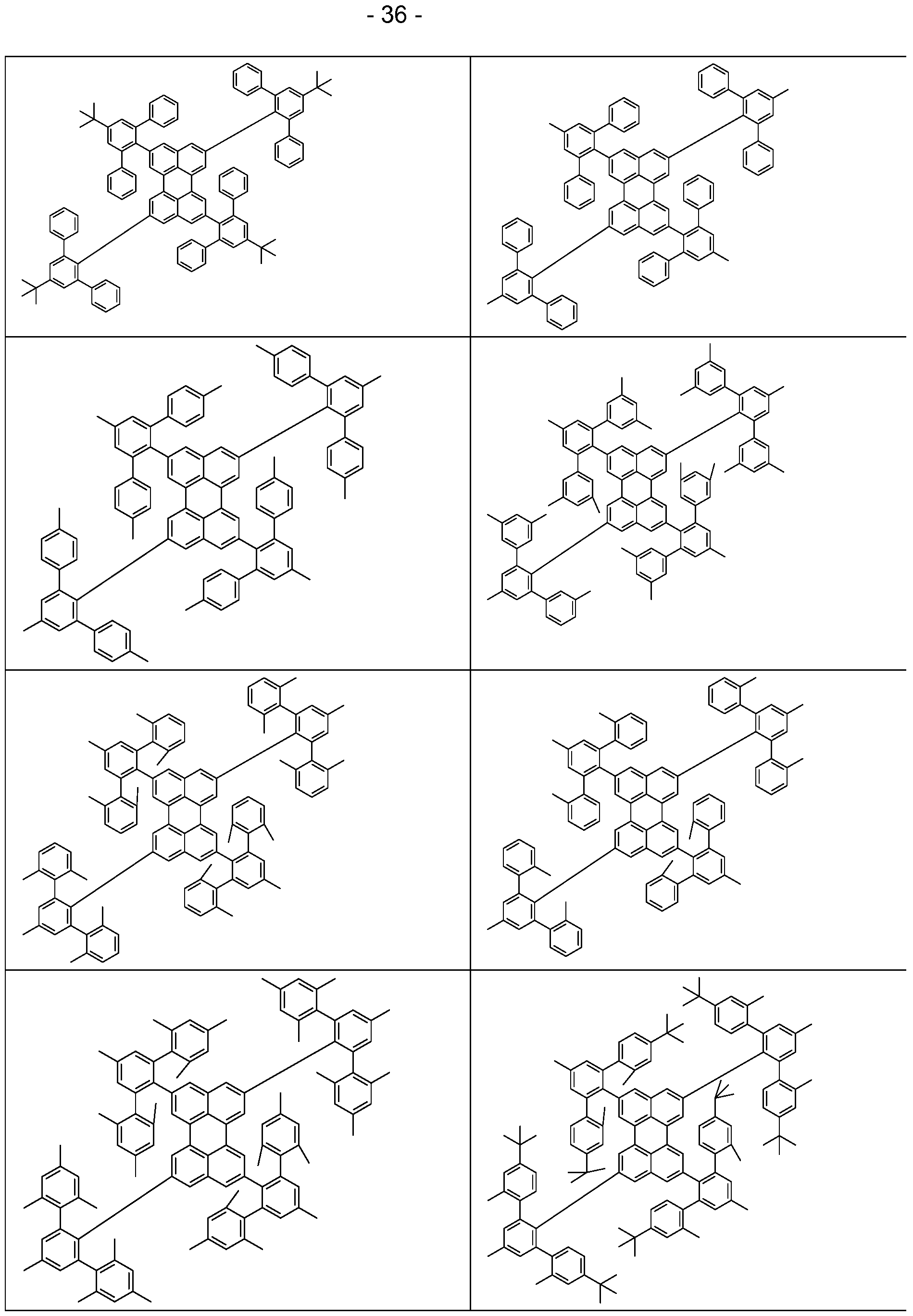
- Preferred fluorescent compounds are rigid tt systems which are substituted with large aliphatic or cycloaliphatic radicals.
- aromatic substituents which can be substituted by aliphatic or cycloaliphatic radicals, are also suitable if these are arranged sterically in such a way that they are not active groups in the sense of the present invention, that is to say their proportion in the relevant molecular orbitals is below a limit as described below.
- aryl amino substituents or heteroaryl groups for example, are too strongly involved in HOMO (highest occupied molecular orbital) or LUMO (lowest unoccupied molecular orbital) and are therefore not suitable as shielding groups.
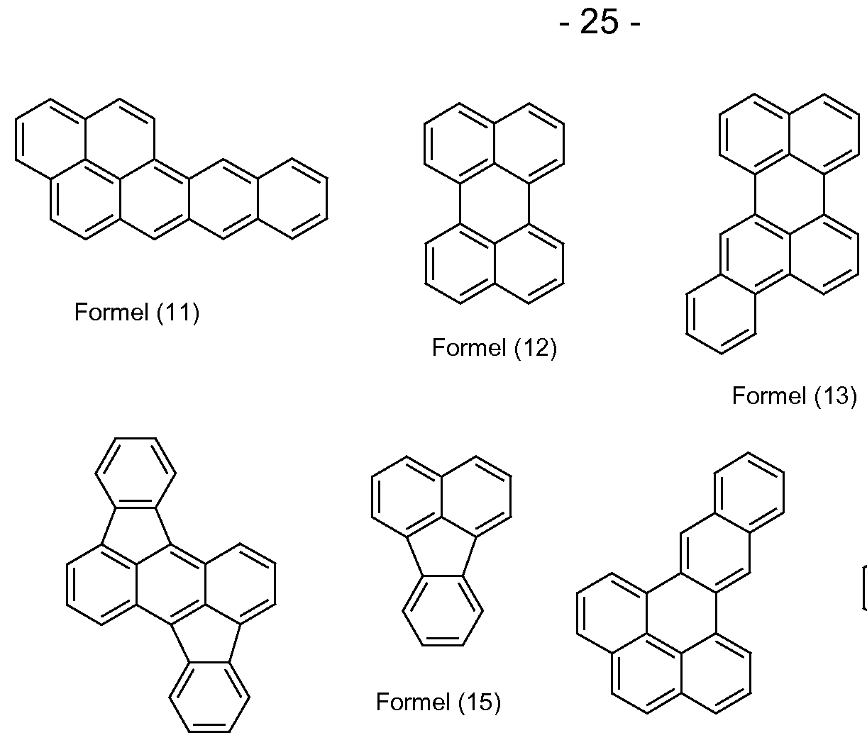
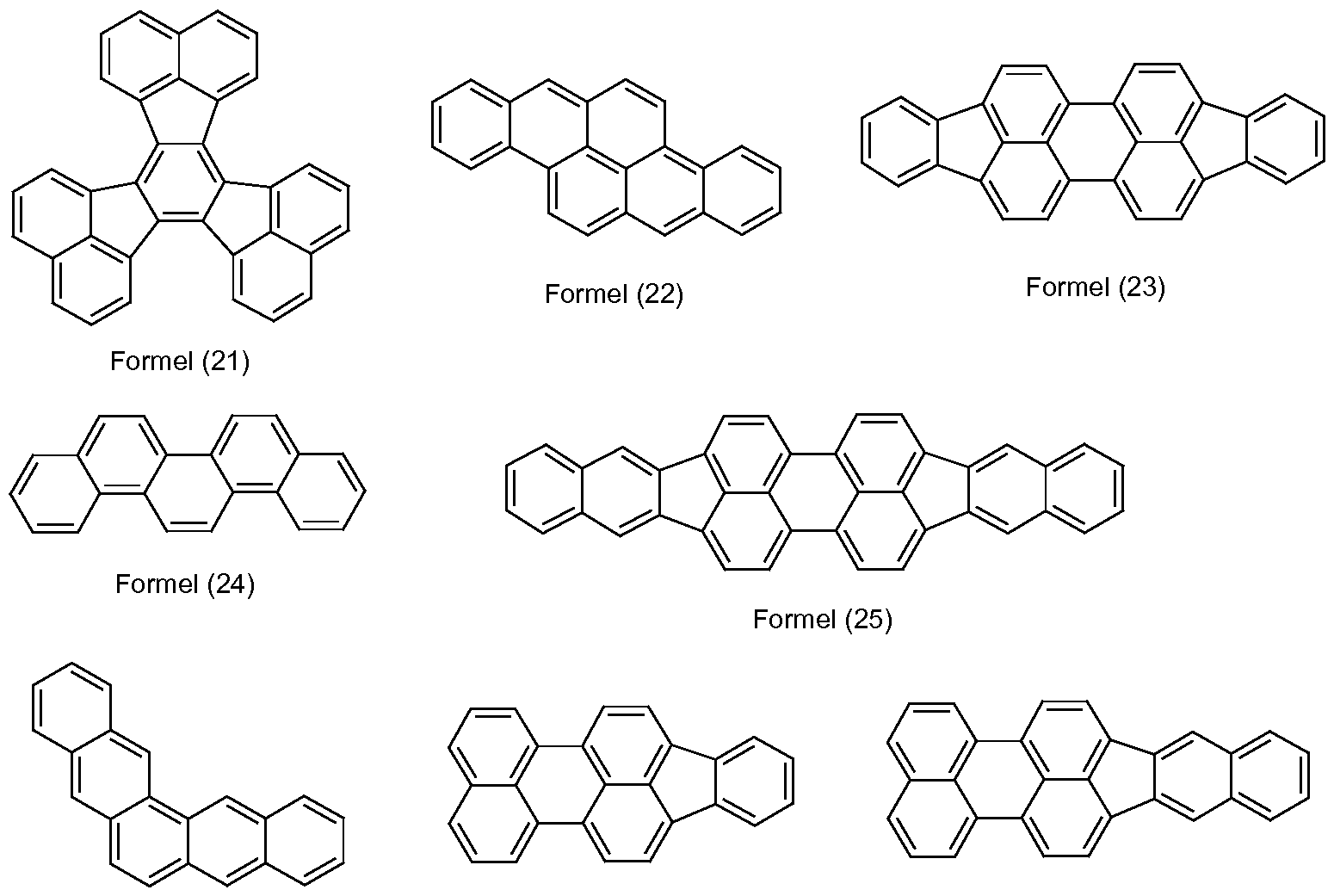
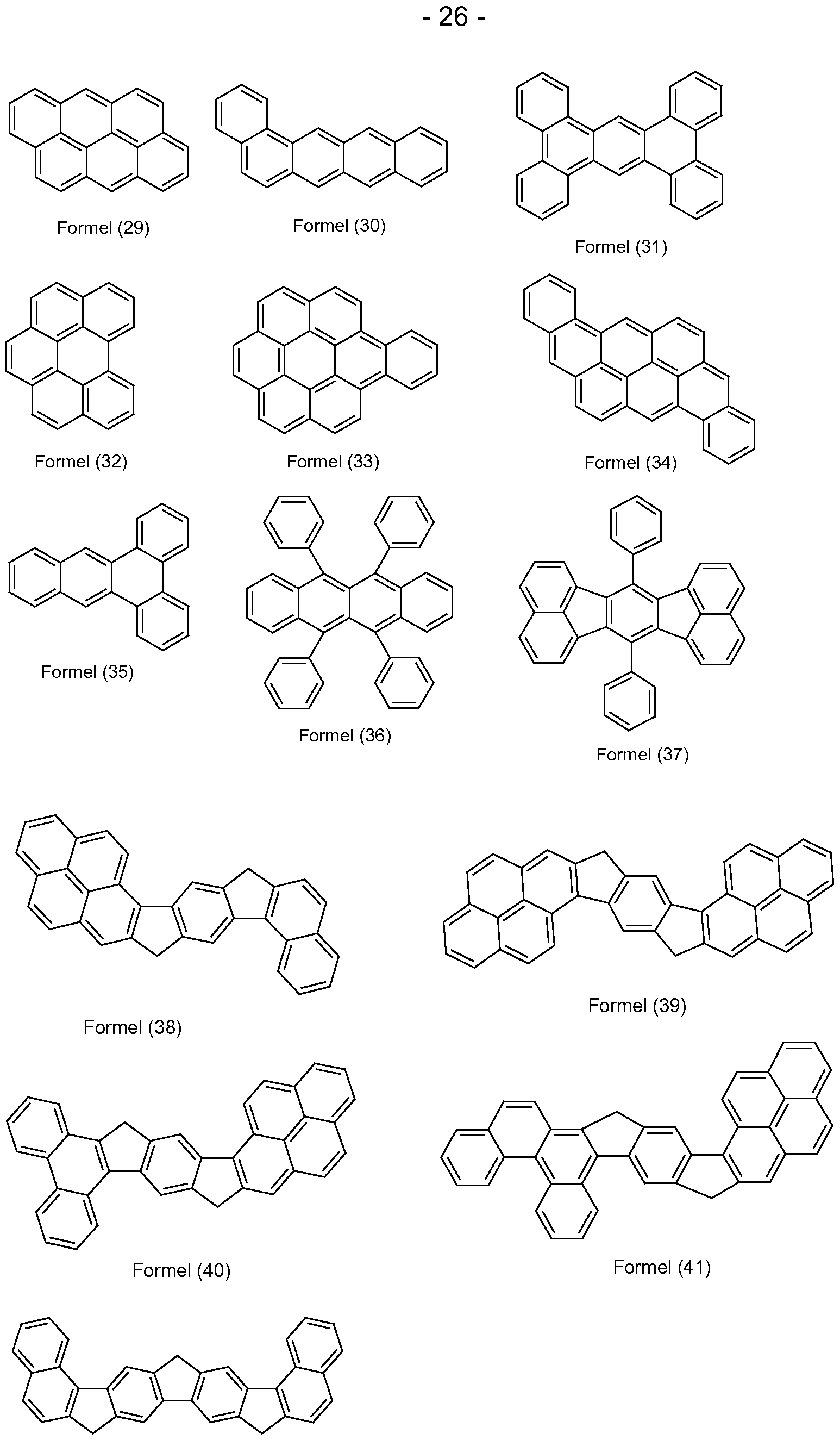
- aromatic bases of fluorescent compounds are the groups of the formulas (1) to (50) listed below,
- suitable heteroaromatic bases of fluorescent compounds are the above-mentioned groups of formulas (1) to (50), in which one, two, three or four carbon atoms of the condensed aromatic nucleus are replaced by nitrogen.
- One, two or three carbon atoms are preferably replaced by nitrogen, oxygen or boron, particularly preferably one or two carbon atoms and very particularly preferably exactly one carbon atom.
- suitable heteroaromatic base bodies of fluorescent compounds are furthermore the groups of the formulas (51) to (73) listed below,
- these structures are substituted by sterically demanding substituents and can also be substituted by further substituents which cannot be regarded as sterically demanding, provided that these substituents are not electronically active or are in turn substituted by sterically shielded substituents are.
- Suitable sterically demanding substituents are, for example, alkyl groups, in particular with 3 to 20 C atoms, preferably with 4 to 10 C atoms, in which H atoms can also be replaced by F, alkoxy groups, in particular with 3 to 20 C atoms Atoms, preferably with 4 to 10 carbon atoms, aralkyl groups, in particular with 7 to 30 carbon atoms, and aromatic ring systems, in particular with 6 to 30 carbon atoms, the aryl groups in the aralkyl groups and aromatic ring systems also being represented by one or several alkyl groups with 1 to 10 carbon atoms can be substituted.
- Several adjacent substituents can also form a ring system with one another.
- the substituent is an aralkyl group or an aromatic ring system
- these have no condensed aryl groups with more than 10 carbon atoms in which aryl groups are directly fused to one another via a common edge. It particularly preferably has no condensed aryl groups in which aryl groups are directly fused to one another via a common edge. So it is preferred if the aromatic ring system, for example, no anthracene or
- Has pyrene groups and particularly preferred if the aromatic ring system also has no naphthalene groups.
- it can have, for example, biphenyl or terphenyl groups, since these have no condensed aryl groups.
- it can also have, for example, fluorene or spirobifluorene groups, since in these groups no aryl groups are directly fused to one another via a common edge.
- this alkyl group preferably has 4 to 10 C atoms. It is preferably a secondary, tertiary or cyclic alkyl group in which the secondary or tertiary carbon atom is either bound directly to the fluorescent base or is bonded to the fluorescent base via a CFh group.
- This alkyl group is particularly preferably selected from the structures of the following formulas (R-1) to (R-33):
- this alkoxy group preferably has 3 to 10 C atoms and is preferably branched or cyclic.
- This alkoxy group is preferably selected from the structures of the following formulas (R-34) to (R-47):
- the dashed bond indicates the attachment of these groups to the fluorescent base.
- this aralkyl group is preferably selected from the structures of the following formulas (R-48) to (R-61):
- R a is selected identically or differently from the group consisting of H, D, F, a straight-chain alkyl group with 1 to 40 C atoms or a branched or cyclic alkyl group with 3 to 40 C atoms, each with one or a plurality of radicals R b can be substituted, an aromatic ring system with 5 to 60 aromatic ring atoms, which can each be substituted with one or more radicals R b , or an aralkyl group with 5 to 60 aromatic ring atoms, which can be substituted with one or more radicals R b can be, optionally two or more adjacent substituents R a can form a ring system which can be substituted with one or more radicals R b ;
- R b is selected from the group consisting of H, D, F, an aliphatic hydrocarbon radical with 1 to 20 C atoms, an aromatic ring system with 5 to 30 aromatic ring atoms, two or more adjacent substituents R b being a ring system
- an aromatic ring system Connection with an aromatic ring system is sterically shielded. If the sterically demanding substituent stands for an aromatic ring system, then this aromatic ring system has 6 to 60 and preferably 6 to 30 aromatic ring atoms, particularly preferably 6 to 24 aromatic ring atoms. This also contains aromatic
- Ring system prefers only phenyl groups.
- the aromatic ring system is preferably selected from the structures of the following formulas (R-62) to (R-76):
- the dashed bond indicates the attachment of these groups to the fluorescent base and the phenyl groups can each be substituted by one or more radicals R a , where R a is defined as indicated above.
- the fluorescent emitter is a purely organic compound without metals or metal ions, which is selected from the group of polycyclic, condensed aromatics with 6 to 60 aromatic ring atoms.
- condensed aromatics pyrenes, perylenes, rubrenes, anthracenes, tetracenes, phenanthrenes, fluorenes and indenofluorenes are particularly preferred, the aromatics preferably being able to be substituted with aromatic ring systems, as already explained in detail elsewhere.
- Perylenes and rubrenes are most preferred for the purposes of the present invention.
- fluorescent emitters are suitable:
- the teaching according to the invention covers the entire range of emissions, both with regard to the fluorescent emitters (in the photoluminescence spectrum) and the emission of the electronic device according to the invention (in the electroluminescence spectrum).
- the fluorescent emitters have a blue emission, with blue emission of the fluorescent emitter preferably being understood as an emission in which the global
- Emission maximum in the phololuminescence spectrum of the fluorescent emitters is in the range from 380 to 500 nm. It is also preferred if the electronic according to the invention
- blue emission from the electronic device preferably being understood to mean an emission in which the global emission maximum in the electroluminescence spectrum of the electronic device according to the invention is in the range from 380 to 500 nm.
- the fluorescent emitters have a green emission, wherein green emission of the fluorescent emitter is preferably understood to mean an emission in which the global emission maximum in the phospholuminescence spectrum of the fluorescent emitters is in the range from 501 to 570 nm.
- the green emission of the electronic device preferably being understood as an emission in which the global emission maximum in the electroluminescence spectrum of the electronic device according to the invention is in the range from 501 to 570 nm.
- the fluorescent emitters have a yellow emission, wherein yellow emission of the fluorescent emitter is preferably understood to mean an emission in which the global emission maximum in the phospholuminescence spectrum of the fluorescent emitters is in the range from 571 to 590 nm.
- the yellow emission of the electronic device preferably being understood to mean an emission in which the global emission maximum in the electroluminescence spectrum of the electronic device according to the invention is in the range from 571 to 590 nm.
- the fluorescent emitters have a red emission, the red emission of the fluorescent emitter preferably being understood as an emission in which the global Emission maximum in the phololuminescence spectrum of the fluorescent emitters is in the range from 591 to 750 nm.
- the red emission of the electronic device preferably being understood as an emission in which the global emission maximum in the electroluminescence spectrum of the electronic device according to the invention is in the range from 591 to 750 nm.
- the sensitizer and the fluorescent emitter can be in the same layer of an electronic device or in different ones
- Sensitizer and fluorescent emitter in the same layer which layer is preferably the emission layer of an electroluminescent device.
- the layer or the composition according to the invention mentioned below containing the sensitizer and the fluorescent emitter preferably contains at least one further material from the group of electron transport materials, hole conductor materials, quantum materials (preferably quantum dots), bipolar hosts, host materials with a wide band gap (wide band gap materials), phosphorescent compounds, fluorescent compounds and materials that exhibit delayed fluorescence.
- Wide band gap materials mean materials that have a large band gap between the HOMO and the LUMO
- Delayed fluorescence materials are preferably those that have thermally induced time-delayed fluorescence (TADF).
- TADF materials have a small distance between the Si and Ti energy level which is preferably 0.3 eV or less, very preferably 0.2 eV or less and very particularly preferably 0.1 eV or less.
- the Si and Ti energies are to be calculated using the quantum chemical method specified below. Examples of common TADF materials can be found in the prior art (e.g. Y. Liu et al., Nature Reviews Materials, Vol. 3, 18020, 2018; Z. Yang et al., Chem. Soc. Rev., 2017, 46 , 915).
- the lowest triplet state Ti is defined as the energy of the triplet state with the lowest energy, which results from the quantum chemical calculation described.
- the lowest excited singlet state Si is defined as the energy of the excited singlet state with the lowest energy, which results from the quantum chemical calculation described.
- Suitable, preferred matrix materials which can be used in combination with the sensitizer and the fluorescent emitter in the emission layer of the electronic device or the compositions according to the invention mentioned below are aromatic ketones, aromatic phosphine oxides or aromatic sulfoxides or sulfones, e.g. B. according to WO 2004/013080, WO 2004/093207, WO 2006/005627 or WO 2010/006680, triarylamines, in particular monoamines, e.g. B. according to WO 2014/015935, carbazole derivatives, e.g. B.
- CBP N, N-biscarbazolylbiphenyl
- carbazole derivatives for example those disclosed in WO 2005/039246, US 2005/0069729, JP 2004/288381, EP 1205527 or WO 2008/086851.
- azacarbazole derivatives e.g. B. according to EP 1617710, EP 1617711, EP 1731584, JP 2005/347160, bipolar matrix materials, e.g. B. according to WO 2007/137725, silanes, e.g. B. according to WO 005/111172, Azaborole or Boronester, z. B. according to WO 2006/117052, triazine derivatives, for. B. according to WO 2010/015306, WO 2007/063754 or WO 2008/056746, zinc complexes, e.g. B.
- diazasilol or tetraazasilol derivatives for. B. according to WO 2010/054729, diazaphosphole derivatives, for. B. according to WO 2010/054730, bridged carbazole derivatives, for. B. according to US 2009/0136779, WO 2010/050778, WO 2011/042107, WO 2011/088877 or WO 2012/143080, triphenylene derivatives, e.g. B. according to WO
- lactams e.g. B. according to WO 2011/116865, WO 2011/137951 or WO 2013/064206, 4-spirocarbazole derivatives, e.g. B. according to WO
- Emission layer or the composition may be present.
- the further material is preferably selected from the group of electron transport materials and from this in particular from the group of pyridines, pyrimidines, pyrazines, pyridazines, triazines, quinazolines, quinoxalines, quinolines, isoquinolines, imidazoles, lactams, dibenzofurans, dibenzothiophenes and / or benzimidazoles , in which
- the further material is selected from the group of the hole transport materials, the carbazoles, biscarbazoles, arlyamines, triarylamines, indenocarbazoles and
- Indolocarbazoles are very particularly preferred.
- the layer containing the sensitizer and the fluorescent emitter and the further material contains at least a fourth material, which can be selected again from the group of the preferred further materials already mentioned above.
- the layer which contains the sensitizer and the fluorescent emitter consists exclusively of the sensitizer and the fluorescent emitter, the layer preferably being the emission layer.
- the sensitizer and the fluorescent emitter are located in different layers, the two layers directly adjoining one another.
- a plurality of layers, each containing a sensitizer and a fluorescent emitter in alternating form, can also adjoin one another.
- the present invention therefore also relates to an electronic device which has an area with the layer sequence
- [SL / FEL] contains n-SL, where n is an integer from 1 to 5, SL is a layer containing the sensitizer and FEL is a layer containing the fluorescent emitters, and wherein the sensitizers in the different layers SL can be different from one another and wherein the fluorescent emitters in different layers FEL can be different from one another.
- the electronic device according to the invention is preferably an organic electronic device and very preferably an organic electronic device from the group of organic electroluminescent devices, organic integrated circuits, organic field-effect transistors, organic
- Thin film transistors organic light-emitting transistors, organic solar cells, organic optical detectors, organic photoreceptors, organic field quench devices, light-emitting electrochemical cells or organic laser diodes.
- the electronic device is very particularly preferably one
- organic electroluminescent device It is even more preferred if the electronic device is an organic electroluminescent device from the group of OLEDs or OLECs, the OLEDs being most preferred.
- Organic electroluminescent devices are a preferred embodiment of the invention.
- the organic electroluminescent device contains cathode, anode and at least one emitting layer. In addition to these layers, it can also contain further layers, for example one or more hole injection layers, hole transport layers, hole blocking layers, electron transport layers, electron injection layers, exciton blocking layers, electron blocking layers, charge generation layers and / or organic or inorganic p / n transitions. It is possible that one or more hole transport layers are p-doped, for example with metal oxides such as M0O3 or WO3 or with (per) fluorinated electron-poor aromatics, and / or that one or more electron transport layers are n-doped.
- interlayers can be introduced between two emitting layers which, for example, have an exciton-blocking function and / or the charge balance in the electroluminescent layer. control the control device.
- each of these layers need not necessarily be present.
- the organic electroluminescent device can be a
- Tandem OLEDs are also preferred. It can also be a hybrid system, where one or more layers fluoresce and one or more other layers phosphoresce.
- Metals with low work function, metal alloys or multi-layer structures made of different metals are preferred as cathode, such as, for example, alkaline earth metals, alkali metals, main group metals or lanthanoids (e.g. Ca, Ba, Mg, Al, In, Mg, Yb, Sm, etc.) . Alloys made of an alkali or alkaline earth metal and silver are also suitable, for example an alloy of magnesium and silver.
- other metals can also be used in addition to the metals mentioned, which have a relatively high work function, such as, for example, B. Ag, in which case combinations of the metals, such as Mg / Ag, Ca / Ag or Ba / Ag are usually used.
- a thin intermediate layer of a material with a high dielectric constant between a metallic cathode and the organic semiconductor for example, alkali metal or alkaline earth metal fluorides, but also the corresponding oxides or carbonates are possible (e.g. LiF, L12O, BaF2, MgO, NaF, CsF, CS2CO3, etc.). Organic alkali metal complexes are also possible, e.g. B. Liq (lithium quinolinate).
- the layer thickness of this layer is preferably between 0.5 and 5 nm. Materials with a high work function are preferred as the anode.
- the anode preferably has a work function greater than 4.5 eV vs. Vacuum on.
- metals with a high redox potential are suitable for this, such as Ag, Pt or Au.
- metal / metal oxide electrodes eg Al / Ni / NiOx, Al / PtOx
- at least one of the electrodes must be transparent or partially transparent in order to enable either the irradiation of the organic material (O-SC) or the coupling out of light (OLED / PLED, O-LASER).
- Preferred anode materials here are conductive mixed metal oxides. Indium tin oxide (ITO) or indium zinc oxide (IZO) are particularly preferred.
- conductive, doped organic materials in particular conductive doped polymers, e.g. B.
- PEDOT, PANI or derivatives of these polymers It is further preferred if a p-doped hole transport material is applied as a hole injection layer to the anode, metal oxides, for example M0O3 or WO3, or (per) fluorinated electron-deficient aromatics being suitable as p-dopants.
- metal oxides for example M0O3 or WO3, or (per) fluorinated electron-deficient aromatics being suitable as p-dopants.
- Other suitable p-dopants are HAT-CN (hexacyano-hexaazatriphenylene) or the compound NPD9 from Novaled. Such a layer simplifies hole injection in materials with a deep HOMO, i.e. one
- the present invention further relates to a composition
- a composition comprising at least one sensitizer and at least one
- the sensitizer and the fluorescent emitter are the compounds mentioned in the present invention. Furthermore, the preferred embodiments of the two components of the composition, that is to say for the sensitizer and the fluorescent emitter, in the sense of the present invention already apply here disclosed preferences described in connection with the electronic device.
- the fluorescent emitter and the sensitizer of the composition at least one of the above-mentioned conditions (I) or (II) has to be fulfilled, whereby it is preferred if condition (I) is fulfilled, and also here the above-mentioned preferences , for example, with respect to X and Y apply.
- the fluorescent emitter of the composition is a sterically shielded compound which has a shielding factor (SF) of greater than or equal to 0.45, preferably greater than or equal to 0.5, very preferably greater than or equal to 0.6 and particularly preferably greater than or equal to 0.65 having.
- SF shielding factor
- Composition containing at least one sensitizer which contains a phosphorescent organometallic complex containing Ir or Pt and a sterically shielded fluorescent emitter with one of the shielding factors listed above.
- composition containing at least one sensitizer which contains a phosphorescent organometallic complex containing Ir or Pt and a fluorescent emitter is very preferred, at least one of the two conditions (I) or (II) having to be fulfilled.
- compositions mentioned preferably contain at least one further material, which is preferably selected from the group of electron transport materials, electron injection materials,
- Electron blocking materials hole transport materials, hole injection materials, hole blocking materials, n-dopants, p-dopants ,,
- Quantum materials preferably quantum dots
- host or quantum dots preferably quantum dots
- Emitters fluorescent emitters or emitters that are delayed Fluorescence, the materials being related to the
- the composition according to the invention preferably contains the sensitizer in a concentration of 5 to 99.9% by weight, very preferably 5 to 60% by weight, particularly preferably 10 to 50% by weight, very particularly preferably 20 to 40% by weight. %, where the information relates to the entire composition.
- the composition according to the invention preferably contains the fluorescent emitter in a concentration of 0.1 to 25% by weight, very preferably 1 to 20% by weight, particularly preferably 3 to 10% by weight, the information relating to the entire composition Respectively.
- the present invention also relates to a formulation comprising the composition mentioned and at least one
- Suitable solvents are preferably organic solvents, such as, for example, alcohols, aldehydes, ketones, ethers, esters, amides, Di C1-C-2-alkylformamides, sulfur compounds, nitrogen compounds,
- Hydrocarbons halogenated hydrocarbons (e.g. chlorinated hydrocarbons), aromatic or heteroaromatic hydrocarbons, halogenated hydrocarbons (e.g. chlorinated hydrocarbons), aromatic or heteroaromatics
- Hydrocarbons and halogenated aromatic or heteroaromatic hydrocarbons Hydrocarbons and halogenated aromatic or heteroaromatic hydrocarbons.
- Preferred solvents can be selected from the following group: substituted and unsubstituted aromatic or linear esters, for example ethyl benzoate, butyl benzoate, octyl octanoate, diethyl sebacate; substituted and unsubstituted aromatic or linear esters, for example 3-phenoxytoluene, 3,4-dimethylanisole, phenetol or anisole; substituted and unsubstituted arenes such as toluene, xylene, pentylbenzene, hexylbenzene, Cyclohexylbenzene, 2-methylbiphenyl, 2,2'-dimethylbiphenyl; Indanes, for example hexamethylindane; substituted and unsubstituted aromatic or linear ketones; substituted and unsubstituted heterocycles, e.g.
- Pyrrolidinones cyclic or non-cyclic siloxanes, pyridines, pyrazines; or other fluorinated or chlorinated aromatic hydrocarbons.
- Particularly preferred solvents are, for example, 1, 2,3,4-tetramethylbenzene, 1, 2,3,5-tetramethylbenzene, 1, 2,3-trimethylbenzene, 1, 2,4,5-tetramethylbenzene, 1, 2.4 -Trichlorobenzen, 1, 2,4-trimethyl-benzene, 1,2-dihydronaphthalene, 1,2-dimethylnaphthalene, 1,3-benzo-dioxolane, 1,3-diisopropylbenzen, 1,3-dimethylnaphthalene, 1,4-benzo -dioxane, 1, 4-diisopropylbenzene, 1, 4-dimethylnaphthalene, 1, 5-dimethyl-tetralin, 1
- Benzonitrile benzothiazole, benzyl acetate, bromobenzen, butyl benzoate, butylphenyl ether, cyclohexyl benzene, decahydronaphthol, dimethoxy toluene, 3-phenoxy toluene, diphenyl ether, propiophenone, ethyl benzene,
- the present invention also relates to an electronic one
- composition especially in the emission layer of a
- the present invention also relates to a method for
- the present invention also relates to a method for producing an electronic device, the composition according to the invention being used to evaporate at least one layer of the electronic device from the vacuum.
- the device is structured accordingly (depending on the application), contacted and finally hermetically sealed, since the life of such devices is drastically shortened in the presence of water and / or air.
- an electronic device in particular an organic electroluminescent device, which is characterized in that one or more layers are coated using a sublimation process.
- the materials are evaporated in vacuum sublimation systems at an initial pressure of typically less than 10 5 mbar, preferably less than 10 6 mbar. It is also possible that the initial pressure is still lower or even higher, for example less than 10 7 mbar.
- an electronic device in particular an organic electroluminescent device, which is characterized in that one or more layers are coated with the OVPD (Organic Vapor Phase Deposition) process or with the aid of a carrier gas sublimation.
- the materials are applied at a pressure between 10 5 mbar and 1 bar.
- the process is the OVJP (Organic Vapor Jet Printing) process, in which the materials are applied directly through a nozzle and structured in this way (for example BMS Arnold et al., Appl. Phys. Lett. 2008, 92, 053301).
- OVJP Organic Vapor Jet Printing
- an electronic device in particular an organic electroluminescent device, which is characterized in that one or more layers of solution, such as. B. by
- the electronic device especially the organic one
- Electroluminescent device can also be manufactured as a hybrid system by applying one or more layers of solution and evaporating one or more other layers. For example, it is possible to apply an emitting layer containing a composition according to the invention from solution and to evaporate a hole blocking layer and / or an electron transport layer thereon in vacuo.
- Figure 1 shows the photoluminescence spectra of the compounds FE-03 and PS-01.
- Figure 2 shows the electroluminescence spectrum from experiment 6.
- compositions according to the invention have improved performance data, in particular efficiency, service life and operating voltage compared to compounds and compositions from the prior art.
- compositions according to the invention allow a practicable or somewhat increased concentration of
- compositions and formulations according to the invention allow simple, inexpensive processing of electronic devices, for example also simple processing from solution. They are therefore suitable for commercial use and mass production.
- compositions and formulations according to the invention have improved stability, which facilitates the storage of the compositions and formulations.
- the respective material is dissolved in toluene.
- a concentration of 1 mg / 100 ml is used.
- the solution is excited in a Hitachi F-4500 fluorescence spectrometer with a wavelength adapted to the material to be examined. The measurement is carried out at room temperature.
- the peak emission wavelength max is the wavelength at which the resulting emission spectrum reaches its first maximum, starting from small wavelengths ( Figure 1).
- the first maximum is typically also the global maximum of the spectrum. If the first maximum of the
- Emission spectrum does not correspond to the global maximum, however, the first maximum has a high intensity in the normalized
- the intensity of the first maximum then being at least 0.5 or more.
- Sensitizers and fluorescent emitters in Table 1.
- the shielding factor (SF) is also listed for the fluorescent emitters.
- perylenes used herein can be made according to the principle outlined below.
- 2,5,8,1 1-tetra- (4,4,5,5-tetramethyl-1, 3,2-dioxaborolan-2-yl) is -Perylene (38.0 g, 50.3 mmol, 1.0 equiv.), 3-phenyl- [1, 1 biphenyl] -2-yl-trifluoromethanesulfonate (95.1 g, 251 .3 mmol, 5.0 equiv.), Tetrakis (triphenylphosphine ) -Palladium (5.81 g, 5.0 mmol, 0.1 equiv.) And Natirum-Metaborate-tetrahydrate (69.3 g, 502.5 mmol, 10.0 equiv.) submitted.
- Tetrakis (triphenylphoshin) palladium (6.11 g, 5.3 mmol, 0.1 equiv.) Is then added and the reaction mixture is degassed for a further 20 min. The reaction is then stirred under reflux for 72 h. The reaction mixture is filtered off. The mother liquor is concentrated, the resulting suspension is filtered and methanol (1000 ml) is added to the mother liquor resulting therefrom. A solid precipitates out. All solids are combined and extracted hot three times over AlOx with toluene. Yet another hot extraction is carried out over AlOx with a mixture of toluene and heptane (1: 1).
- the resulting solid is recrystallized twice from toluene and once from 1 -4-dioxane.
- the desired product is isolated as a yellow solid (5.0 g, 7.47 mmol, 14.1%).
- the solid is then sublimed (4.5 g, 6.73 mmol, 12.7%).
- the OLEDs are encapsulated to protect them against oxygen and water vapor.
- the exact layer structure of the electroluminescent OLEDs can be found in the examples.
- the materials required to manufacture the OLEDs are shown in Table 4.
- the emission layer or layers always consist of at least one matrix material (host material), one
- Sensitizer and fluorescent emitter (FE) are added to the host material (H) by cover vaporization in a certain volume fraction.
- An indication like H-01 S-01 (5%) PE-01 (3%) means that the material H-01 in a volume fraction of 92%, PS-01 in a fraction of 5% and FE-01 in there is a 3% share in the layer.
- the electron transport layer can also consist of a mixture of two
- the OLEDs are characterized by default. For this, the electroluminescence spectra (EL) and voltage-current luminance (UIL) characteristics are measured, which results in the assumption of a
- Lambertian radiation characteristic allows the external quantum efficiency (EQE, measured in percent) to be determined.
- the specification U100 denotes the voltage required for a luminance of 100 cd / m 2 .
- EQE100 denotes the external quantum efficiency at an operating luminance of 100 cd / m 2 .
- the service life LD is defined as the time after which the luminance drops from the starting luminance to a certain proportion L1 during operation with constant current.
- the compounds PS-01, PS-02, PS-03, PS-04 and PS-05 are used as phosphorescent sensitizers.
- the materials FE-01, FE-02, FE-03, FE-04, FE-05, FE-06 and FE-07 are used as fluorescent emitters.
- the OLEDs consist of the following layer sequence, which follows the
- PEDOT PSS treatment is applied to the substrate:
- Table 2 shows the results for various combinations of host, sensitizer and fluorescent emitter.
- the EQE and tension at 100 cd / m 2 are given for the corresponding experiments.
- X stands for Si K (FE) -Si K (S) and Y for Si max (FE) -Si max (S).
- the lifetime of the OLED increases significantly (e.g. Exp. 8 vs. Exp. 6)
- the OLEDs consist of the following layer sequence, which is applied to the substrate: 20 nm HTM: p-D (95%: 5%), 30 nm HTM, 10 nm H-02,
Abstract
Description


Claims
Priority Applications (6)
| Application Number | Priority Date | Filing Date | Title |
|---|---|---|---|
| KR1020217010393A KR20210055756A (en) | 2018-09-12 | 2019-09-12 | Electroluminescent device |
| JP2021514109A JP2022500871A (en) | 2018-09-12 | 2019-09-12 | Electroluminescent device |
| US17/276,060 US20220045276A1 (en) | 2018-09-12 | 2019-09-12 | Electroluminescent devices |
| EP19768792.4A EP3850679A1 (en) | 2018-09-12 | 2019-09-12 | Electroluminescent devices |
| DE112019004560.1T DE112019004560A5 (en) | 2018-09-12 | 2019-09-12 | ELECTROLUMINESCENT DEVICES |
| CN201980059822.8A CN112640147A (en) | 2018-09-12 | 2019-09-12 | Electroluminescent device |
Applications Claiming Priority (2)
| Application Number | Priority Date | Filing Date | Title |
|---|---|---|---|
| EP18194110 | 2018-09-12 | ||
| EP18194110.5 | 2018-09-12 |
Publications (1)
| Publication Number | Publication Date |
|---|---|
| WO2020053314A1 true WO2020053314A1 (en) | 2020-03-19 |
Family
ID=63579103
Family Applications (1)
| Application Number | Title | Priority Date | Filing Date |
|---|---|---|---|
| PCT/EP2019/074290 WO2020053314A1 (en) | 2018-09-12 | 2019-09-12 | Electroluminescent devices |
Country Status (8)
| Country | Link |
|---|---|
| US (1) | US20220045276A1 (en) |
| EP (1) | EP3850679A1 (en) |
| JP (1) | JP2022500871A (en) |
| KR (1) | KR20210055756A (en) |
| CN (1) | CN112640147A (en) |
| DE (2) | DE112019004560A5 (en) |
| TW (1) | TW202030902A (en) |
| WO (1) | WO2020053314A1 (en) |
Cited By (9)
| Publication number | Priority date | Publication date | Assignee | Title |
|---|---|---|---|---|
| WO2022129114A1 (en) | 2020-12-18 | 2022-06-23 | Merck Patent Gmbh | Nitrogenous compounds for organic electroluminescent devices |
| WO2022129116A1 (en) | 2020-12-18 | 2022-06-23 | Merck Patent Gmbh | Indolo[3.2.1-jk]carbazole-6-carbonitrile derivatives as blue fluorescent emitters for use in oleds |
| WO2022129113A1 (en) | 2020-12-18 | 2022-06-23 | Merck Patent Gmbh | Nitrogenous heteroaromatic compounds for organic electroluminescent devices |
| WO2022156313A1 (en) * | 2021-01-25 | 2022-07-28 | 京东方科技集团股份有限公司 | Material for forming blue light-emitting layer, light-emitting device, light-emitting substrate, and light-emitting apparatus |
| WO2022229234A1 (en) | 2021-04-30 | 2022-11-03 | Merck Patent Gmbh | Nitrogenous heterocyclic compounds for organic electroluminescent devices |
| WO2023041454A1 (en) | 2021-09-14 | 2023-03-23 | Merck Patent Gmbh | Boronic heterocyclic compounds for organic electroluminescent devices |
| WO2023072799A1 (en) | 2021-10-27 | 2023-05-04 | Merck Patent Gmbh | Boronic and nitrogenous heterocyclic compounds for organic electroluminescent devices |
| WO2023161168A1 (en) | 2022-02-23 | 2023-08-31 | Merck Patent Gmbh | Aromatic hetreocycles for organic electroluminescent devices |
| WO2023161167A1 (en) | 2022-02-23 | 2023-08-31 | Merck Patent Gmbh | Nitrogenous heterocycles for organic electroluminescent devices |
Families Citing this family (1)
| Publication number | Priority date | Publication date | Assignee | Title |
|---|---|---|---|---|
| TWI826522B (en) * | 2018-09-12 | 2023-12-21 | 德商麥克專利有限公司 | Electroluminescent devices |
Citations (126)
| Publication number | Priority date | Publication date | Assignee | Title |
|---|---|---|---|---|
| US4539507A (en) | 1983-03-25 | 1985-09-03 | Eastman Kodak Company | Organic electroluminescent devices having improved power conversion efficiencies |
| US5151629A (en) | 1991-08-01 | 1992-09-29 | Eastman Kodak Company | Blue emitting internal junction organic electroluminescent device (I) |
| EP0652273A1 (en) | 1993-11-09 | 1995-05-10 | Shinko Electric Industries Co. Ltd. | Organic material for electroluminescent device and electroluminescent device |
| EP0676461A2 (en) | 1994-04-07 | 1995-10-11 | Hoechst Aktiengesellschaft | Spiro compounds and their application as electroluminescence materials |
| WO1998027136A1 (en) | 1996-12-16 | 1998-06-25 | Aventis Research & Technologies Gmbh & Co Kg | ARYL-SUBSTITUTED POLY(p-ARYLENE VINYLENES), METHOD FOR THE PRODUCTION AND USE THEREOF IN ELECTROLUMINESCENT COMPONENTS |
| WO2000070655A2 (en) | 1999-05-13 | 2000-11-23 | The Trustees Of Princeton University | Very high efficiency organic light emitting devices based on electrophosphorescence |
| WO2001041512A1 (en) | 1999-12-01 | 2001-06-07 | The Trustees Of Princeton University | Complexes of form l2mx as phosphorescent dopants for organic leds |
| WO2002002714A2 (en) | 2000-06-30 | 2002-01-10 | E.I. Du Pont De Nemours And Company | Electroluminescent iridium compounds with fluorinated phenylpyridines, phenylpyrimidines, and phenylquinolines and devices made with such compounds |
| WO2002015645A1 (en) | 2000-08-11 | 2002-02-21 | The Trustees Of Princeton University | Organometallic compounds and emission-shifting organic electrophosphorescence |
| EP1191612A2 (en) | 2000-09-26 | 2002-03-27 | Canon Kabushiki Kaisha | Luminescence device, display apparatus and metal coordination compound |
| EP1205527A1 (en) | 2000-03-27 | 2002-05-15 | Idemitsu Kosan Co., Ltd. | Organic electroluminescence device |
| WO2004013080A1 (en) | 2002-08-01 | 2004-02-12 | Covion Organic Semiconductors Gmbh | Spirobifluorene derivatives, their preparation and uses thereof |
| WO2004081017A1 (en) | 2003-03-11 | 2004-09-23 | Covion Organic Semiconductors Gmbh | Metal complexes |
| JP2004288381A (en) | 2003-03-19 | 2004-10-14 | Konica Minolta Holdings Inc | Organic electroluminescent element |
| WO2004093207A2 (en) | 2003-04-15 | 2004-10-28 | Covion Organic Semiconductors Gmbh | Mixtures of matrix materials and organic semiconductors capable of emission, use of the same and electronic components containing said mixtures |
| WO2005011013A1 (en) | 2003-07-21 | 2005-02-03 | Covion Organic Semiconductors Gmbh | Organic electroluminescent element |
| WO2005019373A2 (en) | 2003-08-19 | 2005-03-03 | Basf Aktiengesellschaft | Transition metal complexes comprising carbene ligands serving as emitters for organic light-emitting diodes (oled's) |
| US20050069729A1 (en) | 2003-09-30 | 2005-03-31 | Konica Minolta Holdings, Inc. | Organic electroluminescent element, illuminator, display and compound |
| WO2005033244A1 (en) | 2003-09-29 | 2005-04-14 | Covion Organic Semiconductors Gmbh | Metal complexes |
| WO2005042550A1 (en) | 2003-10-30 | 2005-05-12 | Merck Patent Gmbh | Metal complexes with bipodal ligands |
| US20050170206A1 (en) | 2004-02-03 | 2005-08-04 | Bin Ma | OLEDs utilizing multidentate ligand systems |
| WO2005111172A2 (en) | 2004-05-11 | 2005-11-24 | Merck Patent Gmbh | Novel material mixtures for use in electroluminescence |
| US20050258742A1 (en) | 2004-05-18 | 2005-11-24 | Yui-Yi Tsai | Carbene containing metal complexes as OLEDs |
| JP2005347160A (en) | 2004-06-04 | 2005-12-15 | Konica Minolta Holdings Inc | Organic electroluminescent element, lighting device, and display device |
| EP1617710A1 (en) | 2003-04-23 | 2006-01-18 | Konica Minolta Holdings, Inc. | Material for organic electroluminescent device, organic electroluminescent device, illuminating device and display |
| WO2006005627A1 (en) | 2004-07-15 | 2006-01-19 | Merck Patent Gmbh | Oligomeric derivatives of spirobifluorene, their preparation and use |
| WO2006056418A2 (en) | 2004-11-25 | 2006-06-01 | Basf Aktiengesellschaft | Use of transition metal carbene complexes in organic light-emitting diodes (oleds) |
| WO2006117052A1 (en) | 2005-05-03 | 2006-11-09 | Merck Patent Gmbh | Organic electroluminescent device and boric acid and borinic acid derivatives used therein |
| WO2006121811A1 (en) | 2005-05-06 | 2006-11-16 | Universal Display Corporation | Stability oled materials and devices with improved stability |
| EP1731584A1 (en) | 2004-03-31 | 2006-12-13 | Konica Minolta Holdings, Inc. | Organic electroluminescent device material, organic electroluminescent device, display and illuminating device |
| WO2007063754A1 (en) | 2005-12-01 | 2007-06-07 | Nippon Steel Chemical Co., Ltd. | Compound for organic electroluminescent element and organic electroluminescent element |
| WO2007095118A2 (en) | 2006-02-10 | 2007-08-23 | Universal Display Corporation | METAL COMPLEXES OF CYCLOMETALLATED IMIDAZO[1,2-f]PHENANTHRIDINE AND DIIMIDAZO[1,2-A:1',2'-C]QUINAZOLINE LIGANDS AND ISOELECTRONIC AND BENZANNULATED ANALOGS THEREOF |
| WO2007115981A1 (en) | 2006-04-04 | 2007-10-18 | Basf Se | Transition metal complexes comprising one noncarbene ligand and one or two carbene ligands and their use in oleds |
| WO2007115970A1 (en) | 2006-04-05 | 2007-10-18 | Basf Se | Heteroleptic transition metal-carbene complexes and their use in organic light-emitting diodes (oleds) |
| WO2007137725A1 (en) | 2006-05-31 | 2007-12-06 | Merck Patent Gmbh | New materials for organic electroluminescent devices |
| WO2008000726A1 (en) | 2006-06-26 | 2008-01-03 | Basf Se | Use of pt- and pd-bis- and tetra-carbon complexes with bridged carbon ligands in oleds |
| WO2008000727A1 (en) | 2006-06-26 | 2008-01-03 | Basf Se | Use in oleds of transition metal carbene complexes that contain no cyclometallation via non-carbenes |
| WO2008056746A1 (en) | 2006-11-09 | 2008-05-15 | Nippon Steel Chemical Co., Ltd. | Compound for organic electroluminescent device and organic electroluminescent device |
| WO2008086851A1 (en) | 2007-01-18 | 2008-07-24 | Merck Patent Gmbh | Carbazole derivatives for organc electroluminescent devices |
| WO2008156879A1 (en) | 2007-06-20 | 2008-12-24 | Universal Display Corporation | Blue phosphorescent imidazophenanthridine materials |
| WO2009050290A1 (en) | 2007-10-17 | 2009-04-23 | Basf Se | Transition metal complexes having bridged carbene ligands and the use thereof in oleds |
| WO2009050281A1 (en) | 2007-10-17 | 2009-04-23 | Basf Se | Transition metal complexes with bridged carbene ligands and use thereof in oleds |
| WO2009062578A1 (en) | 2007-11-12 | 2009-05-22 | Merck Patent Gmbh | Organic electroluminescent devices comprising azomethine-metal complexes |
| US20090136779A1 (en) | 2007-11-26 | 2009-05-28 | Chien-Hong Cheng | Conjugated compounds containing hydroindoloacridine structural elements, and their use |
| WO2009146770A2 (en) | 2008-06-05 | 2009-12-10 | Merck Patent Gmbh | Electronic device comprising metal complexes |
| WO2010006680A1 (en) | 2008-07-18 | 2010-01-21 | Merck Patent Gmbh | Materials for organic electroluminescence devices |
| WO2010015306A1 (en) | 2008-08-08 | 2010-02-11 | Merck Patent Gmbh, | Organic electroluminescence device |
| WO2010015307A1 (en) | 2008-08-04 | 2010-02-11 | Merck Patent Gmbh | Electronic devices comprising metal complexes having isonitrile ligands |
| WO2010031485A1 (en) | 2008-09-22 | 2010-03-25 | Merck Patent Gmbh | Materials for organic electroluminescence devices |
| WO2010050778A1 (en) | 2008-10-31 | 2010-05-06 | Gracel Display Inc. | Novel compounds for organic electronic material and organic electronic device using the same |
| WO2010054729A2 (en) | 2008-11-11 | 2010-05-20 | Merck Patent Gmbh | Materials for organic electroluminescence devices |
| WO2010054730A1 (en) | 2008-11-11 | 2010-05-20 | Merck Patent Gmbh | Organic electroluminescent devices |
| WO2010054728A1 (en) | 2008-11-13 | 2010-05-20 | Merck Patent Gmbh | Materials for organic electroluminescent devices |
| WO2010054731A1 (en) | 2008-11-13 | 2010-05-20 | Merck Patent Gmbh | Materials for organic electroluminescent devices |
| WO2010068876A1 (en) | 2008-12-12 | 2010-06-17 | Universal Display Corporation | BLUE EMITTER WITH HIGH EFFICIENCY BASED ON IMIDAZO [1,2-f] PHENANTHRIDINE IRIDIUM COMPLEXES |
| WO2010069442A1 (en) | 2008-12-17 | 2010-06-24 | Merck Patent Gmbh | Organic electroluminescence device |
| WO2010086089A1 (en) | 2009-02-02 | 2010-08-05 | Merck Patent Gmbh | Metal complexes |
| WO2010099852A1 (en) | 2009-03-02 | 2010-09-10 | Merck Patent Gmbh | Metal complexes having azaborol ligands and electronic device having the same |
| WO2010102709A1 (en) | 2009-03-13 | 2010-09-16 | Merck Patent Gmbh | Materials for organic electroluminescence devices |
| WO2010136109A1 (en) | 2009-05-29 | 2010-12-02 | Merck Patent Gmbh | Materials for organic electroluminescent devices |
| WO2011000455A1 (en) | 2009-06-30 | 2011-01-06 | Merck Patent Gmbh | Materials for organic electroluminescence devices |
| WO2011032626A1 (en) | 2009-09-16 | 2011-03-24 | Merck Patent Gmbh | Metal complexes |
| WO2011042107A2 (en) | 2009-10-08 | 2011-04-14 | Merck Patent Gmbh | Materials for organic electroluminescent devices |
| WO2011045337A1 (en) | 2009-10-14 | 2011-04-21 | Basf Se | Dinuclear platinum-carbene complexes and the use thereof in oleds |
| WO2011044988A1 (en) | 2009-10-16 | 2011-04-21 | Merck Patent Gmbh | Metal complexes |
| WO2011051404A1 (en) | 2009-10-28 | 2011-05-05 | Basf Se | Heteroleptic carbene complexes and use thereof in organic electronics |
| WO2011066898A1 (en) | 2009-12-05 | 2011-06-09 | Merck Patent Gmbh | Electronic device containing metal complexes |
| WO2011073149A1 (en) | 2009-12-14 | 2011-06-23 | Basf Se | Metal complexes comprising diazabenzimidazol carbene-ligands and the use thereof in oleds |
| WO2011088877A1 (en) | 2010-01-25 | 2011-07-28 | Merck Patent Gmbh | Compounds for electronic devices |
| WO2011106344A1 (en) | 2010-02-25 | 2011-09-01 | Universal Display Corporation | Phosphorescent emitters |
| WO2011116865A1 (en) | 2010-03-25 | 2011-09-29 | Merck Patent Gmbh | Materials for organic electroluminescence devices |
| WO2011137951A1 (en) | 2010-05-04 | 2011-11-10 | Merck Patent Gmbh | Organic electroluminescence devices |
| US20110303903A1 (en) * | 2008-08-05 | 2011-12-15 | Sony Corporation | Organic electroluminescence element and display device |
| WO2011157339A1 (en) | 2010-06-15 | 2011-12-22 | Merck Patent Gmbh | Metal complexes |
| WO2012007086A1 (en) | 2010-07-16 | 2012-01-19 | Merck Patent Gmbh | Metal complexes |
| WO2012048781A1 (en) | 2010-10-15 | 2012-04-19 | Merck Patent Gmbh | Triphenylene-based materials for organic electroluminescent devices |
| WO2012121936A2 (en) | 2011-03-08 | 2012-09-13 | Universal Display Corporation | Pyridyl carbene phosphorescent emitters |
| WO2012143080A2 (en) | 2011-04-18 | 2012-10-26 | Merck Patent Gmbh | Materials for organic electroluminescent devices |
| WO2012156378A1 (en) | 2011-05-13 | 2012-11-22 | Cynora Gmbh | Copper(i) complexes, in particular for optoelectronic components |
| US20120305894A1 (en) | 2011-06-01 | 2012-12-06 | Do-Han Kim | Blue phosphorescent compound and organic electroluminescent device using the same |
| WO2012163471A1 (en) | 2011-06-03 | 2012-12-06 | Merck Patent Gmbh | Metal complexes |
| WO2012170571A1 (en) | 2011-06-08 | 2012-12-13 | Universal Display Corporation | Heteroleptic iridium carbene complexes and light emitting device using them |
| WO2012172482A1 (en) | 2011-06-14 | 2012-12-20 | Basf Se | Metal complexes comprising azabenzimidazole carbene ligands and the use thereof in oleds |
| WO2013001086A1 (en) | 2011-06-29 | 2013-01-03 | Cynora Gmbh | Copper(i) complexes, in particular for optoelectronic components |
| EP2543672A1 (en) | 2011-07-08 | 2013-01-09 | cynora GmbH | Copper(I) complexes, in particular for optoelectronic components |
| WO2013007707A1 (en) | 2011-07-08 | 2013-01-17 | Cynora Gmbh | Copper(i) complexes for optoelectronic devices |
| WO2013017675A1 (en) | 2011-08-02 | 2013-02-07 | Cynora Gmbh | Singlet harvesting with dual-core copper (i) complexes for optoelectronic devices |
| WO2013020631A1 (en) | 2011-08-10 | 2013-02-14 | Merck Patent Gmbh | Metal complexes |
| WO2013064206A1 (en) | 2011-11-01 | 2013-05-10 | Merck Patent Gmbh | Organic electroluminescent device |
| WO2013072508A1 (en) | 2011-11-16 | 2013-05-23 | Cynora Gmbh | Heteroleptic copper complexes for optoelectronic uses |
| US20130150581A1 (en) | 2010-07-20 | 2013-06-13 | Cynora Gmbh | Copper (i) complexes for optoelectronic devices |
| WO2014008982A1 (en) | 2012-07-13 | 2014-01-16 | Merck Patent Gmbh | Metal complexes |
| WO2014015935A2 (en) | 2012-07-23 | 2014-01-30 | Merck Patent Gmbh | Compounds and organic electronic devices |
| WO2014023377A2 (en) | 2012-08-07 | 2014-02-13 | Merck Patent Gmbh | Metal complexes |
| WO2014094961A1 (en) | 2012-12-21 | 2014-06-26 | Merck Patent Gmbh | Metal complexes |
| WO2014094963A1 (en) | 2012-12-21 | 2014-06-26 | Merck Patent Gmbh | Materials for organic electroluminescent devices |
| WO2014109814A2 (en) | 2012-10-26 | 2014-07-17 | Arizona Board Of Regents Acting For And On Behalf Of Arizona State University | Metal complexes, methods, and uses thereof |
| WO2015014944A1 (en) | 2013-07-31 | 2015-02-05 | Basf Se | Luminescent diaza- monoaza- and benzimidazole metal carbene complexes for use in electronic devices such as oleds |
| WO2015036074A1 (en) | 2013-09-11 | 2015-03-19 | Merck Patent Gmbh | Metal complexes |
| US20150171350A1 (en) | 2012-07-19 | 2015-06-18 | Basf Se | Dinuclear metal complexes comprising carbene ligands and the use thereof in oleds |
| WO2015091716A1 (en) | 2013-12-20 | 2015-06-25 | Basf Se | Highly efficient oled devices with very short decay times |
| WO2015104045A1 (en) | 2014-01-13 | 2015-07-16 | Merck Patent Gmbh | Metal complexes |
| WO2015117718A1 (en) | 2014-02-05 | 2015-08-13 | Merck Patent Gmbh | Metal complexes |
| US20150243912A1 (en) | 2012-08-09 | 2015-08-27 | Basf Se | Transition metal complexes with carbene ligands and the use thereof in oleds |
| WO2015135624A1 (en) | 2014-03-13 | 2015-09-17 | Merck Patent Gmbh | Organic electroluminescent device |
| WO2015169412A1 (en) | 2014-05-05 | 2015-11-12 | Merck Patent Gmbh | Materials for organic light emitting devices |
| WO2015192939A1 (en) | 2014-06-18 | 2015-12-23 | Merck Patent Gmbh | Materials for organic electroluminescent devices |
| WO2016015810A1 (en) | 2014-07-29 | 2016-02-04 | Merck Patent Gmbh | Materials for organic electroluminescent devices |
| WO2016015815A1 (en) | 2014-07-28 | 2016-02-04 | Merck Patent Gmbh | Metal complexes |
| WO2016020516A1 (en) | 2014-08-08 | 2016-02-11 | Basf Se | Electroluminescent imidazo-quinoxaline carbene metal complexes |
| WO2016023608A1 (en) | 2014-08-13 | 2016-02-18 | Merck Patent Gmbh | Materials for organic electroluminescent devices |
| US20160072081A1 (en) | 2013-04-29 | 2016-03-10 | Basf Se | Transition metal complexes with carbene ligands and the use thereof in OLEDs |
| WO2016079169A1 (en) | 2014-11-18 | 2016-05-26 | Basf Se | Pt- or pd-carbene complexes for use in organic light emitting diodes |
| WO2016124304A1 (en) | 2015-02-03 | 2016-08-11 | Merck Patent Gmbh | Metal complexes |
| WO2016193243A1 (en) | 2015-06-03 | 2016-12-08 | Udc Ireland Limited | Highly efficient oled devices with very short decay times |
| EP3126371A1 (en) | 2014-03-31 | 2017-02-08 | UDC Ireland Limited | Metal complexes, comprising carbene ligands having an o-substituted non-cyclometalated aryl group and their use in organic light emitting diodes |
| WO2017032439A1 (en) | 2015-08-25 | 2017-03-02 | Merck Patent Gmbh | Metal complexes |
| EP3184534A1 (en) | 2015-12-21 | 2017-06-28 | UDC Ireland Limited | Transition metal complexes with tripodal ligands and the use thereof in oleds |
| WO2018011186A1 (en) | 2016-07-14 | 2018-01-18 | Merck Patent Gmbh | Metal complexes |
| WO2018019687A1 (en) | 2016-07-25 | 2018-02-01 | Merck Patent Gmbh | Dinuclear and oligonuclear metal complexes containing tripodal bidentate part ligands and their use in electronic devices |
| WO2018019688A1 (en) | 2016-07-25 | 2018-02-01 | Merck Patent Gmbh | Metal complexes for use as emitters in organic electroluminescence devices |
| WO2018041769A1 (en) | 2016-08-30 | 2018-03-08 | Merck Patent Gmbh | Binuclear and trinuclear metal complexes composed of two inter-linked tripodal hexadentate ligands for use in electroluminescent devices |
| WO2018054798A1 (en) | 2016-09-21 | 2018-03-29 | Merck Patent Gmbh | Binuclear metal complexes for use as emitters in organic electroluminescent devices |
| WO2018069196A1 (en) | 2016-10-12 | 2018-04-19 | Merck Patent Gmbh | Binuclear metal complexes and electronic devices, in particular organic electroluminescent devices containing said metal complexes |
| WO2018069273A1 (en) | 2016-10-13 | 2018-04-19 | Merck Patent Gmbh | Metal complexes |
| WO2018069197A1 (en) | 2016-10-12 | 2018-04-19 | Merck Patent Gmbh | Metal complexes |
Family Cites Families (4)
| Publication number | Priority date | Publication date | Assignee | Title |
|---|---|---|---|---|
| JP4039023B2 (en) * | 2000-10-04 | 2008-01-30 | 三菱化学株式会社 | Organic electroluminescence device |
| JP2005310766A (en) * | 2004-03-26 | 2005-11-04 | Fuji Photo Film Co Ltd | Organic electroluminescent element |
| JP4214482B2 (en) * | 2004-08-26 | 2009-01-28 | 独立行政法人科学技術振興機構 | Organic electroluminescence device |
| KR20170038681A (en) * | 2015-09-30 | 2017-04-07 | 가부시키가이샤 한도오따이 에네루기 켄큐쇼 | Light-emitting element, display device, electronic device, and lighting device |
-
2019
- 2019-09-11 TW TW108132760A patent/TW202030902A/en unknown
- 2019-09-12 KR KR1020217010393A patent/KR20210055756A/en not_active Application Discontinuation
- 2019-09-12 DE DE112019004560.1T patent/DE112019004560A5/en active Pending
- 2019-09-12 CN CN201980059822.8A patent/CN112640147A/en active Pending
- 2019-09-12 DE DE202019005923.7U patent/DE202019005923U1/en active Active
- 2019-09-12 US US17/276,060 patent/US20220045276A1/en active Pending
- 2019-09-12 EP EP19768792.4A patent/EP3850679A1/en active Pending
- 2019-09-12 JP JP2021514109A patent/JP2022500871A/en active Pending
- 2019-09-12 WO PCT/EP2019/074290 patent/WO2020053314A1/en unknown
Patent Citations (131)
| Publication number | Priority date | Publication date | Assignee | Title |
|---|---|---|---|---|
| US4539507A (en) | 1983-03-25 | 1985-09-03 | Eastman Kodak Company | Organic electroluminescent devices having improved power conversion efficiencies |
| US5151629A (en) | 1991-08-01 | 1992-09-29 | Eastman Kodak Company | Blue emitting internal junction organic electroluminescent device (I) |
| EP0652273A1 (en) | 1993-11-09 | 1995-05-10 | Shinko Electric Industries Co. Ltd. | Organic material for electroluminescent device and electroluminescent device |
| EP0676461A2 (en) | 1994-04-07 | 1995-10-11 | Hoechst Aktiengesellschaft | Spiro compounds and their application as electroluminescence materials |
| WO1998027136A1 (en) | 1996-12-16 | 1998-06-25 | Aventis Research & Technologies Gmbh & Co Kg | ARYL-SUBSTITUTED POLY(p-ARYLENE VINYLENES), METHOD FOR THE PRODUCTION AND USE THEREOF IN ELECTROLUMINESCENT COMPONENTS |
| WO2000070655A2 (en) | 1999-05-13 | 2000-11-23 | The Trustees Of Princeton University | Very high efficiency organic light emitting devices based on electrophosphorescence |
| WO2001041512A1 (en) | 1999-12-01 | 2001-06-07 | The Trustees Of Princeton University | Complexes of form l2mx as phosphorescent dopants for organic leds |
| EP1205527A1 (en) | 2000-03-27 | 2002-05-15 | Idemitsu Kosan Co., Ltd. | Organic electroluminescence device |
| WO2002002714A2 (en) | 2000-06-30 | 2002-01-10 | E.I. Du Pont De Nemours And Company | Electroluminescent iridium compounds with fluorinated phenylpyridines, phenylpyrimidines, and phenylquinolines and devices made with such compounds |
| WO2002015645A1 (en) | 2000-08-11 | 2002-02-21 | The Trustees Of Princeton University | Organometallic compounds and emission-shifting organic electrophosphorescence |
| EP1191612A2 (en) | 2000-09-26 | 2002-03-27 | Canon Kabushiki Kaisha | Luminescence device, display apparatus and metal coordination compound |
| WO2004013080A1 (en) | 2002-08-01 | 2004-02-12 | Covion Organic Semiconductors Gmbh | Spirobifluorene derivatives, their preparation and uses thereof |
| WO2004081017A1 (en) | 2003-03-11 | 2004-09-23 | Covion Organic Semiconductors Gmbh | Metal complexes |
| JP2004288381A (en) | 2003-03-19 | 2004-10-14 | Konica Minolta Holdings Inc | Organic electroluminescent element |
| WO2004093207A2 (en) | 2003-04-15 | 2004-10-28 | Covion Organic Semiconductors Gmbh | Mixtures of matrix materials and organic semiconductors capable of emission, use of the same and electronic components containing said mixtures |
| EP1617710A1 (en) | 2003-04-23 | 2006-01-18 | Konica Minolta Holdings, Inc. | Material for organic electroluminescent device, organic electroluminescent device, illuminating device and display |
| EP1617711A1 (en) | 2003-04-23 | 2006-01-18 | Konica Minolta Holdings, Inc. | Organic electroluminescent device and display |
| WO2005011013A1 (en) | 2003-07-21 | 2005-02-03 | Covion Organic Semiconductors Gmbh | Organic electroluminescent element |
| WO2005019373A2 (en) | 2003-08-19 | 2005-03-03 | Basf Aktiengesellschaft | Transition metal complexes comprising carbene ligands serving as emitters for organic light-emitting diodes (oled's) |
| WO2005033244A1 (en) | 2003-09-29 | 2005-04-14 | Covion Organic Semiconductors Gmbh | Metal complexes |
| US20050069729A1 (en) | 2003-09-30 | 2005-03-31 | Konica Minolta Holdings, Inc. | Organic electroluminescent element, illuminator, display and compound |
| WO2005039246A1 (en) | 2003-09-30 | 2005-04-28 | Konica Minolta Holdings, Inc. | Organic electroluminescent device, illuminating device, and display |
| WO2005042550A1 (en) | 2003-10-30 | 2005-05-12 | Merck Patent Gmbh | Metal complexes with bipodal ligands |
| US20050170206A1 (en) | 2004-02-03 | 2005-08-04 | Bin Ma | OLEDs utilizing multidentate ligand systems |
| EP1731584A1 (en) | 2004-03-31 | 2006-12-13 | Konica Minolta Holdings, Inc. | Organic electroluminescent device material, organic electroluminescent device, display and illuminating device |
| WO2005111172A2 (en) | 2004-05-11 | 2005-11-24 | Merck Patent Gmbh | Novel material mixtures for use in electroluminescence |
| US20050258742A1 (en) | 2004-05-18 | 2005-11-24 | Yui-Yi Tsai | Carbene containing metal complexes as OLEDs |
| JP2005347160A (en) | 2004-06-04 | 2005-12-15 | Konica Minolta Holdings Inc | Organic electroluminescent element, lighting device, and display device |
| WO2006005627A1 (en) | 2004-07-15 | 2006-01-19 | Merck Patent Gmbh | Oligomeric derivatives of spirobifluorene, their preparation and use |
| WO2006056418A2 (en) | 2004-11-25 | 2006-06-01 | Basf Aktiengesellschaft | Use of transition metal carbene complexes in organic light-emitting diodes (oleds) |
| WO2006117052A1 (en) | 2005-05-03 | 2006-11-09 | Merck Patent Gmbh | Organic electroluminescent device and boric acid and borinic acid derivatives used therein |
| WO2006121811A1 (en) | 2005-05-06 | 2006-11-16 | Universal Display Corporation | Stability oled materials and devices with improved stability |
| WO2007063754A1 (en) | 2005-12-01 | 2007-06-07 | Nippon Steel Chemical Co., Ltd. | Compound for organic electroluminescent element and organic electroluminescent element |
| WO2007095118A2 (en) | 2006-02-10 | 2007-08-23 | Universal Display Corporation | METAL COMPLEXES OF CYCLOMETALLATED IMIDAZO[1,2-f]PHENANTHRIDINE AND DIIMIDAZO[1,2-A:1',2'-C]QUINAZOLINE LIGANDS AND ISOELECTRONIC AND BENZANNULATED ANALOGS THEREOF |
| WO2007115981A1 (en) | 2006-04-04 | 2007-10-18 | Basf Se | Transition metal complexes comprising one noncarbene ligand and one or two carbene ligands and their use in oleds |
| WO2007115970A1 (en) | 2006-04-05 | 2007-10-18 | Basf Se | Heteroleptic transition metal-carbene complexes and their use in organic light-emitting diodes (oleds) |
| WO2007137725A1 (en) | 2006-05-31 | 2007-12-06 | Merck Patent Gmbh | New materials for organic electroluminescent devices |
| WO2008000726A1 (en) | 2006-06-26 | 2008-01-03 | Basf Se | Use of pt- and pd-bis- and tetra-carbon complexes with bridged carbon ligands in oleds |
| WO2008000727A1 (en) | 2006-06-26 | 2008-01-03 | Basf Se | Use in oleds of transition metal carbene complexes that contain no cyclometallation via non-carbenes |
| WO2008056746A1 (en) | 2006-11-09 | 2008-05-15 | Nippon Steel Chemical Co., Ltd. | Compound for organic electroluminescent device and organic electroluminescent device |
| WO2008086851A1 (en) | 2007-01-18 | 2008-07-24 | Merck Patent Gmbh | Carbazole derivatives for organc electroluminescent devices |
| WO2008156879A1 (en) | 2007-06-20 | 2008-12-24 | Universal Display Corporation | Blue phosphorescent imidazophenanthridine materials |
| WO2009050290A1 (en) | 2007-10-17 | 2009-04-23 | Basf Se | Transition metal complexes having bridged carbene ligands and the use thereof in oleds |
| WO2009050281A1 (en) | 2007-10-17 | 2009-04-23 | Basf Se | Transition metal complexes with bridged carbene ligands and use thereof in oleds |
| WO2009062578A1 (en) | 2007-11-12 | 2009-05-22 | Merck Patent Gmbh | Organic electroluminescent devices comprising azomethine-metal complexes |
| US20090136779A1 (en) | 2007-11-26 | 2009-05-28 | Chien-Hong Cheng | Conjugated compounds containing hydroindoloacridine structural elements, and their use |
| WO2009146770A2 (en) | 2008-06-05 | 2009-12-10 | Merck Patent Gmbh | Electronic device comprising metal complexes |
| WO2010006680A1 (en) | 2008-07-18 | 2010-01-21 | Merck Patent Gmbh | Materials for organic electroluminescence devices |
| WO2010015307A1 (en) | 2008-08-04 | 2010-02-11 | Merck Patent Gmbh | Electronic devices comprising metal complexes having isonitrile ligands |
| US20110303903A1 (en) * | 2008-08-05 | 2011-12-15 | Sony Corporation | Organic electroluminescence element and display device |
| WO2010015306A1 (en) | 2008-08-08 | 2010-02-11 | Merck Patent Gmbh, | Organic electroluminescence device |
| WO2010031485A1 (en) | 2008-09-22 | 2010-03-25 | Merck Patent Gmbh | Materials for organic electroluminescence devices |
| WO2010050778A1 (en) | 2008-10-31 | 2010-05-06 | Gracel Display Inc. | Novel compounds for organic electronic material and organic electronic device using the same |
| WO2010054729A2 (en) | 2008-11-11 | 2010-05-20 | Merck Patent Gmbh | Materials for organic electroluminescence devices |
| WO2010054730A1 (en) | 2008-11-11 | 2010-05-20 | Merck Patent Gmbh | Organic electroluminescent devices |
| WO2010054728A1 (en) | 2008-11-13 | 2010-05-20 | Merck Patent Gmbh | Materials for organic electroluminescent devices |
| WO2010054731A1 (en) | 2008-11-13 | 2010-05-20 | Merck Patent Gmbh | Materials for organic electroluminescent devices |
| WO2010068876A1 (en) | 2008-12-12 | 2010-06-17 | Universal Display Corporation | BLUE EMITTER WITH HIGH EFFICIENCY BASED ON IMIDAZO [1,2-f] PHENANTHRIDINE IRIDIUM COMPLEXES |
| WO2010069442A1 (en) | 2008-12-17 | 2010-06-24 | Merck Patent Gmbh | Organic electroluminescence device |
| WO2010086089A1 (en) | 2009-02-02 | 2010-08-05 | Merck Patent Gmbh | Metal complexes |
| WO2010099852A1 (en) | 2009-03-02 | 2010-09-10 | Merck Patent Gmbh | Metal complexes having azaborol ligands and electronic device having the same |
| WO2010102709A1 (en) | 2009-03-13 | 2010-09-16 | Merck Patent Gmbh | Materials for organic electroluminescence devices |
| WO2010136109A1 (en) | 2009-05-29 | 2010-12-02 | Merck Patent Gmbh | Materials for organic electroluminescent devices |
| WO2011000455A1 (en) | 2009-06-30 | 2011-01-06 | Merck Patent Gmbh | Materials for organic electroluminescence devices |
| WO2011032626A1 (en) | 2009-09-16 | 2011-03-24 | Merck Patent Gmbh | Metal complexes |
| WO2011042107A2 (en) | 2009-10-08 | 2011-04-14 | Merck Patent Gmbh | Materials for organic electroluminescent devices |
| WO2011045337A1 (en) | 2009-10-14 | 2011-04-21 | Basf Se | Dinuclear platinum-carbene complexes and the use thereof in oleds |
| WO2011044988A1 (en) | 2009-10-16 | 2011-04-21 | Merck Patent Gmbh | Metal complexes |
| WO2011051404A1 (en) | 2009-10-28 | 2011-05-05 | Basf Se | Heteroleptic carbene complexes and use thereof in organic electronics |
| WO2011066898A1 (en) | 2009-12-05 | 2011-06-09 | Merck Patent Gmbh | Electronic device containing metal complexes |
| WO2011073149A1 (en) | 2009-12-14 | 2011-06-23 | Basf Se | Metal complexes comprising diazabenzimidazol carbene-ligands and the use thereof in oleds |
| WO2011088877A1 (en) | 2010-01-25 | 2011-07-28 | Merck Patent Gmbh | Compounds for electronic devices |
| WO2011106344A1 (en) | 2010-02-25 | 2011-09-01 | Universal Display Corporation | Phosphorescent emitters |
| WO2011116865A1 (en) | 2010-03-25 | 2011-09-29 | Merck Patent Gmbh | Materials for organic electroluminescence devices |
| WO2011137951A1 (en) | 2010-05-04 | 2011-11-10 | Merck Patent Gmbh | Organic electroluminescence devices |
| WO2011157339A1 (en) | 2010-06-15 | 2011-12-22 | Merck Patent Gmbh | Metal complexes |
| WO2012007086A1 (en) | 2010-07-16 | 2012-01-19 | Merck Patent Gmbh | Metal complexes |
| US20130150581A1 (en) | 2010-07-20 | 2013-06-13 | Cynora Gmbh | Copper (i) complexes for optoelectronic devices |
| WO2012048781A1 (en) | 2010-10-15 | 2012-04-19 | Merck Patent Gmbh | Triphenylene-based materials for organic electroluminescent devices |
| WO2012121936A2 (en) | 2011-03-08 | 2012-09-13 | Universal Display Corporation | Pyridyl carbene phosphorescent emitters |
| WO2012143080A2 (en) | 2011-04-18 | 2012-10-26 | Merck Patent Gmbh | Materials for organic electroluminescent devices |
| WO2012156378A1 (en) | 2011-05-13 | 2012-11-22 | Cynora Gmbh | Copper(i) complexes, in particular for optoelectronic components |
| US20120305894A1 (en) | 2011-06-01 | 2012-12-06 | Do-Han Kim | Blue phosphorescent compound and organic electroluminescent device using the same |
| WO2012163471A1 (en) | 2011-06-03 | 2012-12-06 | Merck Patent Gmbh | Metal complexes |
| WO2012170571A1 (en) | 2011-06-08 | 2012-12-13 | Universal Display Corporation | Heteroleptic iridium carbene complexes and light emitting device using them |
| WO2012170463A1 (en) | 2011-06-08 | 2012-12-13 | Universal Display Corporation | Heteroleptic iridium carbene complexes and light emitting device using them |
| WO2012170461A1 (en) | 2011-06-08 | 2012-12-13 | Universal Display Corporation | Heteroleptic iridium carbene complexes and light emitting device using them |
| WO2012172482A1 (en) | 2011-06-14 | 2012-12-20 | Basf Se | Metal complexes comprising azabenzimidazole carbene ligands and the use thereof in oleds |
| WO2013001086A1 (en) | 2011-06-29 | 2013-01-03 | Cynora Gmbh | Copper(i) complexes, in particular for optoelectronic components |
| EP2543672A1 (en) | 2011-07-08 | 2013-01-09 | cynora GmbH | Copper(I) complexes, in particular for optoelectronic components |
| WO2013007707A1 (en) | 2011-07-08 | 2013-01-17 | Cynora Gmbh | Copper(i) complexes for optoelectronic devices |
| WO2013017675A1 (en) | 2011-08-02 | 2013-02-07 | Cynora Gmbh | Singlet harvesting with dual-core copper (i) complexes for optoelectronic devices |
| WO2013020631A1 (en) | 2011-08-10 | 2013-02-14 | Merck Patent Gmbh | Metal complexes |
| WO2013064206A1 (en) | 2011-11-01 | 2013-05-10 | Merck Patent Gmbh | Organic electroluminescent device |
| WO2013072508A1 (en) | 2011-11-16 | 2013-05-23 | Cynora Gmbh | Heteroleptic copper complexes for optoelectronic uses |
| WO2014008982A1 (en) | 2012-07-13 | 2014-01-16 | Merck Patent Gmbh | Metal complexes |
| US20150171350A1 (en) | 2012-07-19 | 2015-06-18 | Basf Se | Dinuclear metal complexes comprising carbene ligands and the use thereof in oleds |
| WO2014015935A2 (en) | 2012-07-23 | 2014-01-30 | Merck Patent Gmbh | Compounds and organic electronic devices |
| WO2014023377A2 (en) | 2012-08-07 | 2014-02-13 | Merck Patent Gmbh | Metal complexes |
| US20150243912A1 (en) | 2012-08-09 | 2015-08-27 | Basf Se | Transition metal complexes with carbene ligands and the use thereof in oleds |
| WO2014109814A2 (en) | 2012-10-26 | 2014-07-17 | Arizona Board Of Regents Acting For And On Behalf Of Arizona State University | Metal complexes, methods, and uses thereof |
| WO2014094961A1 (en) | 2012-12-21 | 2014-06-26 | Merck Patent Gmbh | Metal complexes |
| WO2014094963A1 (en) | 2012-12-21 | 2014-06-26 | Merck Patent Gmbh | Materials for organic electroluminescent devices |
| US20160072081A1 (en) | 2013-04-29 | 2016-03-10 | Basf Se | Transition metal complexes with carbene ligands and the use thereof in OLEDs |
| WO2015014944A1 (en) | 2013-07-31 | 2015-02-05 | Basf Se | Luminescent diaza- monoaza- and benzimidazole metal carbene complexes for use in electronic devices such as oleds |
| WO2015014835A1 (en) | 2013-07-31 | 2015-02-05 | Basf Se | Luminescent diazabenzimidazole carbene metal complexes |
| WO2015036074A1 (en) | 2013-09-11 | 2015-03-19 | Merck Patent Gmbh | Metal complexes |
| WO2015091716A1 (en) | 2013-12-20 | 2015-06-25 | Basf Se | Highly efficient oled devices with very short decay times |
| WO2015104045A1 (en) | 2014-01-13 | 2015-07-16 | Merck Patent Gmbh | Metal complexes |
| WO2015117718A1 (en) | 2014-02-05 | 2015-08-13 | Merck Patent Gmbh | Metal complexes |
| WO2015135624A1 (en) | 2014-03-13 | 2015-09-17 | Merck Patent Gmbh | Organic electroluminescent device |
| EP3126371A1 (en) | 2014-03-31 | 2017-02-08 | UDC Ireland Limited | Metal complexes, comprising carbene ligands having an o-substituted non-cyclometalated aryl group and their use in organic light emitting diodes |
| WO2015169412A1 (en) | 2014-05-05 | 2015-11-12 | Merck Patent Gmbh | Materials for organic light emitting devices |
| WO2015192939A1 (en) | 2014-06-18 | 2015-12-23 | Merck Patent Gmbh | Materials for organic electroluminescent devices |
| WO2016015815A1 (en) | 2014-07-28 | 2016-02-04 | Merck Patent Gmbh | Metal complexes |
| WO2016015810A1 (en) | 2014-07-29 | 2016-02-04 | Merck Patent Gmbh | Materials for organic electroluminescent devices |
| WO2016020516A1 (en) | 2014-08-08 | 2016-02-11 | Basf Se | Electroluminescent imidazo-quinoxaline carbene metal complexes |
| WO2016023608A1 (en) | 2014-08-13 | 2016-02-18 | Merck Patent Gmbh | Materials for organic electroluminescent devices |
| WO2016079169A1 (en) | 2014-11-18 | 2016-05-26 | Basf Se | Pt- or pd-carbene complexes for use in organic light emitting diodes |
| WO2016124304A1 (en) | 2015-02-03 | 2016-08-11 | Merck Patent Gmbh | Metal complexes |
| WO2016193243A1 (en) | 2015-06-03 | 2016-12-08 | Udc Ireland Limited | Highly efficient oled devices with very short decay times |
| WO2017032439A1 (en) | 2015-08-25 | 2017-03-02 | Merck Patent Gmbh | Metal complexes |
| EP3184534A1 (en) | 2015-12-21 | 2017-06-28 | UDC Ireland Limited | Transition metal complexes with tripodal ligands and the use thereof in oleds |
| WO2018011186A1 (en) | 2016-07-14 | 2018-01-18 | Merck Patent Gmbh | Metal complexes |
| WO2018019687A1 (en) | 2016-07-25 | 2018-02-01 | Merck Patent Gmbh | Dinuclear and oligonuclear metal complexes containing tripodal bidentate part ligands and their use in electronic devices |
| WO2018019688A1 (en) | 2016-07-25 | 2018-02-01 | Merck Patent Gmbh | Metal complexes for use as emitters in organic electroluminescence devices |
| WO2018041769A1 (en) | 2016-08-30 | 2018-03-08 | Merck Patent Gmbh | Binuclear and trinuclear metal complexes composed of two inter-linked tripodal hexadentate ligands for use in electroluminescent devices |
| WO2018054798A1 (en) | 2016-09-21 | 2018-03-29 | Merck Patent Gmbh | Binuclear metal complexes for use as emitters in organic electroluminescent devices |
| WO2018069196A1 (en) | 2016-10-12 | 2018-04-19 | Merck Patent Gmbh | Binuclear metal complexes and electronic devices, in particular organic electroluminescent devices containing said metal complexes |
| WO2018069197A1 (en) | 2016-10-12 | 2018-04-19 | Merck Patent Gmbh | Metal complexes |
| WO2018069273A1 (en) | 2016-10-13 | 2018-04-19 | Merck Patent Gmbh | Metal complexes |
Non-Patent Citations (9)
| Title |
|---|
| "Recent progress of molecular organic electroluminescent materials and devices", MAT. SCI. AND ENG. R, vol. 39, 2002, pages 143 - 222 |
| C. H. CHEN ET AL.: "Recent developments in organic electroluminescent materials", MACROMOL. SYMP., vol. 125, 1997, pages 1 - 48, XP000891579 |
| CHENG G ET AL: "Highly efficient white organic light-emitting devices based on a multiple-emissive-layer structure", THIN SOLID FILMS, ELSEVIER, AMSTERDAM, NL, vol. 516, no. 15, 2 June 2008 (2008-06-02), pages 5133 - 5136, XP022622360, ISSN: 0040-6090, [retrieved on 20071203], DOI: 10.1016/J.TSF.2007.10.115 * |
| FREITAG P ET AL: "Lambertian white top-emitting organic light emitting device with carbon nanotube cathode", JOURNAL OF APPLIED PHYSICS, AMERICAN INSTITUTE OF PHYSICS, US, vol. 112, no. 11, 1 December 2012 (2012-12-01), pages 114505 - 114505, XP012167226, ISSN: 0021-8979, [retrieved on 20121204], DOI: 10.1063/1.4767439 * |
| M. S. ARNOLD ET AL., APPL. PHYS. LETT., vol. 92, 2008, pages 053301 |
| MICHEAL L. CONNOLLY: "Computation of Molecular Volume", J. AM. CHEM. SOC., vol. 107, 1985, pages 1118 - 1124 |
| XU DZHANG Y: "Generating Triangulated Macromolecular Surfaces by Euclidean Distance Transform", PLOS ONE, vol. 4, no. 12, 2009, pages e8140 |
| Y. LIU ET AL., NATURE REVIEWS MATERIALS, vol. 3, 2018, pages 18020 |
| Z. YANG ET AL., CHEM. SOC. REV., vol. 46, 2017, pages 915 |
Cited By (9)
| Publication number | Priority date | Publication date | Assignee | Title |
|---|---|---|---|---|
| WO2022129114A1 (en) | 2020-12-18 | 2022-06-23 | Merck Patent Gmbh | Nitrogenous compounds for organic electroluminescent devices |
| WO2022129116A1 (en) | 2020-12-18 | 2022-06-23 | Merck Patent Gmbh | Indolo[3.2.1-jk]carbazole-6-carbonitrile derivatives as blue fluorescent emitters for use in oleds |
| WO2022129113A1 (en) | 2020-12-18 | 2022-06-23 | Merck Patent Gmbh | Nitrogenous heteroaromatic compounds for organic electroluminescent devices |
| WO2022156313A1 (en) * | 2021-01-25 | 2022-07-28 | 京东方科技集团股份有限公司 | Material for forming blue light-emitting layer, light-emitting device, light-emitting substrate, and light-emitting apparatus |
| WO2022229234A1 (en) | 2021-04-30 | 2022-11-03 | Merck Patent Gmbh | Nitrogenous heterocyclic compounds for organic electroluminescent devices |
| WO2023041454A1 (en) | 2021-09-14 | 2023-03-23 | Merck Patent Gmbh | Boronic heterocyclic compounds for organic electroluminescent devices |
| WO2023072799A1 (en) | 2021-10-27 | 2023-05-04 | Merck Patent Gmbh | Boronic and nitrogenous heterocyclic compounds for organic electroluminescent devices |
| WO2023161168A1 (en) | 2022-02-23 | 2023-08-31 | Merck Patent Gmbh | Aromatic hetreocycles for organic electroluminescent devices |
| WO2023161167A1 (en) | 2022-02-23 | 2023-08-31 | Merck Patent Gmbh | Nitrogenous heterocycles for organic electroluminescent devices |
Also Published As
| Publication number | Publication date |
|---|---|
| US20220045276A1 (en) | 2022-02-10 |
| JP2022500871A (en) | 2022-01-04 |
| EP3850679A1 (en) | 2021-07-21 |
| DE112019004560A5 (en) | 2021-05-27 |
| CN112640147A (en) | 2021-04-09 |
| TW202030902A (en) | 2020-08-16 |
| KR20210055756A (en) | 2021-05-17 |
| DE202019005923U1 (en) | 2023-06-27 |
Similar Documents
| Publication | Publication Date | Title |
|---|---|---|
| WO2020053314A1 (en) | Electroluminescent devices | |
| WO2020053315A1 (en) | Electroluminescent devices | |
| DE202019005189U1 (en) | Electroluminescent device | |
| EP3055303B1 (en) | Materials for electronic devices | |
| EP3027708B1 (en) | Materials for electronic devices | |
| DE112011101604B4 (en) | Organic electroluminescent device | |
| DE102009009277B4 (en) | Organic electronic device, process for its production and use of compounds | |
| DE102009012346B4 (en) | Organic electroluminescent device and method for producing the same | |
| WO2017148564A1 (en) | Materials for organic electroluminescent devices | |
| EP3210248B2 (en) | Materials for electronic devices | |
| EP3538623B1 (en) | Compounds with an acceptor and a donor group | |
| EP3371274B1 (en) | Materials for organic electroluminescent devices | |
| DE102014008722A1 (en) | Compositions for electronic devices | |
| EP3016959A1 (en) | Polycyclic compounds | |
| WO2011032624A1 (en) | Organic electroluminescent device | |
| WO2010115498A1 (en) | Organic electroluminescence device | |
| WO2013050101A1 (en) | Organic electroluminescent device | |
| EP4066289A1 (en) | Compounds for electronic devices | |
| EP3928360A1 (en) | Composition for organic electronic devices | |
| EP3036241B1 (en) | Metal complexes | |
| EP3548481B1 (en) | Heterocyclic compounds for use in electronic devices | |
| EP4315444A1 (en) | Organic electroluminescent device |
Legal Events
| Date | Code | Title | Description |
|---|---|---|---|
| 121 | Ep: the epo has been informed by wipo that ep was designated in this application |
Ref document number: 19768792 Country of ref document: EP Kind code of ref document: A1 |
|
| ENP | Entry into the national phase |
Ref document number: 2021514109 Country of ref document: JP Kind code of ref document: A |
|
| ENP | Entry into the national phase |
Ref document number: 20217010393 Country of ref document: KR Kind code of ref document: A |
|
| ENP | Entry into the national phase |
Ref document number: 2019768792 Country of ref document: EP Effective date: 20210412 |
|
| REG | Reference to national code |
Ref country code: DE Ref legal event code: R225 Ref document number: 112019004560 Country of ref document: DE |