WO2020050195A1 - 固体撮像素子および電子装置 - Google Patents
固体撮像素子および電子装置 Download PDFInfo
- Publication number
- WO2020050195A1 WO2020050195A1 PCT/JP2019/034348 JP2019034348W WO2020050195A1 WO 2020050195 A1 WO2020050195 A1 WO 2020050195A1 JP 2019034348 W JP2019034348 W JP 2019034348W WO 2020050195 A1 WO2020050195 A1 WO 2020050195A1
- Authority
- WO
- WIPO (PCT)
- Prior art keywords
- photoelectric conversion
- solid
- state imaging
- conversion element
- imaging device
- Prior art date
- Legal status (The legal status is an assumption and is not a legal conclusion. Google has not performed a legal analysis and makes no representation as to the accuracy of the status listed.)
- Ceased
Links
Images





Classifications
-
- H—ELECTRICITY
- H10—SEMICONDUCTOR DEVICES; ELECTRIC SOLID-STATE DEVICES NOT OTHERWISE PROVIDED FOR
- H10F—INORGANIC SEMICONDUCTOR DEVICES SENSITIVE TO INFRARED RADIATION, LIGHT, ELECTROMAGNETIC RADIATION OF SHORTER WAVELENGTH OR CORPUSCULAR RADIATION
- H10F39/00—Integrated devices, or assemblies of multiple devices, comprising at least one element covered by group H10F30/00, e.g. radiation detectors comprising photodiode arrays
- H10F39/10—Integrated devices
- H10F39/12—Image sensors
- H10F39/199—Back-illuminated image sensors
-
- H—ELECTRICITY
- H04—ELECTRIC COMMUNICATION TECHNIQUE
- H04N—PICTORIAL COMMUNICATION, e.g. TELEVISION
- H04N25/00—Circuitry of solid-state image sensors [SSIS]; Control thereof
- H04N25/70—SSIS architectures; Circuits associated therewith
-
- H—ELECTRICITY
- H04—ELECTRIC COMMUNICATION TECHNIQUE
- H04N—PICTORIAL COMMUNICATION, e.g. TELEVISION
- H04N25/00—Circuitry of solid-state image sensors [SSIS]; Control thereof
- H04N25/70—SSIS architectures; Circuits associated therewith
- H04N25/76—Addressed sensors, e.g. MOS or CMOS sensors
- H04N25/77—Pixel circuitry, e.g. memories, A/D converters, pixel amplifiers, shared circuits or shared components
-
- H—ELECTRICITY
- H10—SEMICONDUCTOR DEVICES; ELECTRIC SOLID-STATE DEVICES NOT OTHERWISE PROVIDED FOR
- H10F—INORGANIC SEMICONDUCTOR DEVICES SENSITIVE TO INFRARED RADIATION, LIGHT, ELECTROMAGNETIC RADIATION OF SHORTER WAVELENGTH OR CORPUSCULAR RADIATION
- H10F39/00—Integrated devices, or assemblies of multiple devices, comprising at least one element covered by group H10F30/00, e.g. radiation detectors comprising photodiode arrays
- H10F39/10—Integrated devices
- H10F39/12—Image sensors
- H10F39/18—Complementary metal-oxide-semiconductor [CMOS] image sensors; Photodiode array image sensors
-
- H—ELECTRICITY
- H10—SEMICONDUCTOR DEVICES; ELECTRIC SOLID-STATE DEVICES NOT OTHERWISE PROVIDED FOR
- H10F—INORGANIC SEMICONDUCTOR DEVICES SENSITIVE TO INFRARED RADIATION, LIGHT, ELECTROMAGNETIC RADIATION OF SHORTER WAVELENGTH OR CORPUSCULAR RADIATION
- H10F39/00—Integrated devices, or assemblies of multiple devices, comprising at least one element covered by group H10F30/00, e.g. radiation detectors comprising photodiode arrays
- H10F39/80—Constructional details of image sensors
- H10F39/803—Pixels having integrated switching, control, storage or amplification elements
- H10F39/8033—Photosensitive area
-
- H—ELECTRICITY
- H10—SEMICONDUCTOR DEVICES; ELECTRIC SOLID-STATE DEVICES NOT OTHERWISE PROVIDED FOR
- H10F—INORGANIC SEMICONDUCTOR DEVICES SENSITIVE TO INFRARED RADIATION, LIGHT, ELECTROMAGNETIC RADIATION OF SHORTER WAVELENGTH OR CORPUSCULAR RADIATION
- H10F39/00—Integrated devices, or assemblies of multiple devices, comprising at least one element covered by group H10F30/00, e.g. radiation detectors comprising photodiode arrays
- H10F39/80—Constructional details of image sensors
- H10F39/803—Pixels having integrated switching, control, storage or amplification elements
- H10F39/8037—Pixels having integrated switching, control, storage or amplification elements the integrated elements comprising a transistor
-
- H—ELECTRICITY
- H10—SEMICONDUCTOR DEVICES; ELECTRIC SOLID-STATE DEVICES NOT OTHERWISE PROVIDED FOR
- H10F—INORGANIC SEMICONDUCTOR DEVICES SENSITIVE TO INFRARED RADIATION, LIGHT, ELECTROMAGNETIC RADIATION OF SHORTER WAVELENGTH OR CORPUSCULAR RADIATION
- H10F39/00—Integrated devices, or assemblies of multiple devices, comprising at least one element covered by group H10F30/00, e.g. radiation detectors comprising photodiode arrays
- H10F39/80—Constructional details of image sensors
- H10F39/807—Pixel isolation structures
-
- H—ELECTRICITY
- H10—SEMICONDUCTOR DEVICES; ELECTRIC SOLID-STATE DEVICES NOT OTHERWISE PROVIDED FOR
- H10F—INORGANIC SEMICONDUCTOR DEVICES SENSITIVE TO INFRARED RADIATION, LIGHT, ELECTROMAGNETIC RADIATION OF SHORTER WAVELENGTH OR CORPUSCULAR RADIATION
- H10F39/00—Integrated devices, or assemblies of multiple devices, comprising at least one element covered by group H10F30/00, e.g. radiation detectors comprising photodiode arrays
- H10F39/80—Constructional details of image sensors
- H10F39/811—Interconnections
-
- H—ELECTRICITY
- H10—SEMICONDUCTOR DEVICES; ELECTRIC SOLID-STATE DEVICES NOT OTHERWISE PROVIDED FOR
- H10F—INORGANIC SEMICONDUCTOR DEVICES SENSITIVE TO INFRARED RADIATION, LIGHT, ELECTROMAGNETIC RADIATION OF SHORTER WAVELENGTH OR CORPUSCULAR RADIATION
- H10F39/00—Integrated devices, or assemblies of multiple devices, comprising at least one element covered by group H10F30/00, e.g. radiation detectors comprising photodiode arrays
- H10F39/80—Constructional details of image sensors
- H10F39/812—Arrangements for transferring the charges in the image sensor perpendicular to the imaging plane, e.g. buried regions used to transfer generated charges to circuitry under the photosensitive region
-
- H—ELECTRICITY
- H10—SEMICONDUCTOR DEVICES; ELECTRIC SOLID-STATE DEVICES NOT OTHERWISE PROVIDED FOR
- H10F—INORGANIC SEMICONDUCTOR DEVICES SENSITIVE TO INFRARED RADIATION, LIGHT, ELECTROMAGNETIC RADIATION OF SHORTER WAVELENGTH OR CORPUSCULAR RADIATION
- H10F39/00—Integrated devices, or assemblies of multiple devices, comprising at least one element covered by group H10F30/00, e.g. radiation detectors comprising photodiode arrays
- H10F39/80—Constructional details of image sensors
- H10F39/813—Electronic components shared by multiple pixels, e.g. one amplifier shared by two pixels
-
- H—ELECTRICITY
- H10—SEMICONDUCTOR DEVICES; ELECTRIC SOLID-STATE DEVICES NOT OTHERWISE PROVIDED FOR
- H10F—INORGANIC SEMICONDUCTOR DEVICES SENSITIVE TO INFRARED RADIATION, LIGHT, ELECTROMAGNETIC RADIATION OF SHORTER WAVELENGTH OR CORPUSCULAR RADIATION
- H10F39/00—Integrated devices, or assemblies of multiple devices, comprising at least one element covered by group H10F30/00, e.g. radiation detectors comprising photodiode arrays
- H10F39/011—Manufacture or treatment of image sensors covered by group H10F39/12
- H10F39/014—Manufacture or treatment of image sensors covered by group H10F39/12 of CMOS image sensors
Definitions
- the present technology relates to a solid-state imaging device. More specifically, the present invention relates to a solid-state imaging device that photoelectrically converts light from a subject and an electronic device.
- a known solid-state image sensor has a function of detecting not only visible light but also ultraviolet light.
- a technique has been proposed in which an ultraviolet light sensitive element and a visible light sensitive element are formed on a semiconductor substrate having an SOI (Silicon On Insulator) structure to be integrated into one chip (for example, see Patent Document 1).
- SOI Silicon On Insulator
- both the visible light sensitive element and the ultraviolet light sensitive element are formed on the silicon substrate.
- this conventional technique has a problem in that resolution is reduced because each light detection area is separately allocated in a plane in order to detect each of ultraviolet light and visible light. Further, since the Bayer arrangement is impossible, there is a problem that the color interpolation processing becomes difficult in addition to the reduction in the resolution.
- the present technology has been created in view of such a situation, and has an object to improve the resolution of a solid-state imaging device that detects visible light and ultraviolet light.
- the present technology has been made to solve the above-described problem, and a first aspect of the present technology is to accumulate a first photoelectric conversion element and a charge photoelectrically converted by the first photoelectric conversion element.
- an electronic device comprising: a connection portion connected to the storage portion for transferring the electric charge stored in the second storage portion to the other surface of the substrate. This brings about an effect of individually performing photoelectric conversion on both surfaces of the substrate.
- the first photoelectric conversion element photoelectrically converts light in a visible light region
- the second photoelectric conversion element is an ultraviolet light.
- the light in the light region may be photoelectrically converted. This brings about an effect that the visible light and the ultraviolet light are photoelectrically converted in one pixel.
- the substrate is a silicon substrate
- the second photoelectric conversion element is formed in a region having a depth of up to 40 nanometers from the surface of one surface of the substrate. You may.
- the first photoelectric conversion element is formed in a surface region of the other surface of the substrate.
- connection portion may be a conductor penetrating the substrate. This brings about an effect that the electric charge accumulated in the second accumulation part is transferred to the other surface through the substrate.
- this conductor may be formed to include at least tungsten.
- a hafnium film may be further provided on the surface of the second storage section. This has the effect of preventing reflection and suppressing dark current.
- a potential barrier may be further provided between the first accumulation unit and the second accumulation unit. This brings about an effect of separating charges of light having different wavelengths.
- the first photoelectric conversion element photoelectrically converts light of a plurality of colors different from each other
- the first storage unit stores the photoelectrically converted charge in a penetrating direction of the substrate. May be stored for each color. This brings about an effect that the color filter for each color becomes unnecessary.
- the second photoelectric conversion element is divided into left and right to perform photoelectric conversion, respectively, and the second storage unit is provided with the left and right divided second photoelectric conversion elements.
- the charge may be divided and stored in accordance with each of them. This brings about an effect that the autofocus is performed by detecting the phase difference based on the charge of the second photoelectric conversion element divided into right and left.
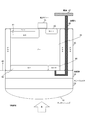
- FIG. 3 is a diagram illustrating a schematic example of a cross section of one pixel of the solid-state imaging device according to the first embodiment of the present technology.
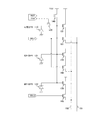
- FIG. 3 is a diagram illustrating an example of an equivalent circuit of one pixel of the solid-state imaging device according to the first embodiment of the present technology.
- FIG. 6 is a diagram illustrating an example of operation timing of the solid-state imaging device according to the first embodiment of the present technology.
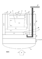
- FIG. 11 is a diagram illustrating a schematic example of a cross section of one pixel of a solid-state imaging device according to a second embodiment of the present technology.
- FIG. 13 is a diagram illustrating a schematic example of a cross section of one pixel of a solid-state imaging device according to a third embodiment of the present technology.
- FIG. 3 is a diagram illustrating a schematic example of a cross section of one pixel of the solid-state imaging device according to the first embodiment of the present technology.
- FIG. 3 is a diagram illustrating an example of an equivalent circuit
- FIG. 13 is a diagram illustrating a schematic example of a cross section of one pixel of a solid-state imaging device according to a fourth embodiment of the present technology.
- FIG. 15 is a diagram illustrating an example of an equivalent circuit of one pixel of a solid-state imaging device according to a fourth embodiment of the present technology.
- FIG. 21 is a diagram illustrating a schematic example of a cross section of one pixel of a solid-state imaging device according to a fifth embodiment of the present technology.
- FIG. 15 is a diagram illustrating an example of an equivalent circuit of one pixel of a solid-state imaging device according to a fifth embodiment of the present technology. It is the first half of the figure showing the example of the manufacturing process of the solid-state image sensing device in an embodiment of the present technology. It is the latter half of the figure showing the example of the manufacturing process of the solid-state image sensing device in an embodiment of the present technology.
- First embodiment (example in which an ultraviolet light detecting photodiode is provided on the back surface side) 2.
- Second embodiment an example in which a hafnium film is deposited on the back surface) 3.
- Third embodiment (example in which a potential barrier is provided immediately below a photodiode for detecting ultraviolet light) 4.
- Fourth embodiment (example in which a photodiode for visible light detection has a vertical spectral structure in silicon) 5.
- Fifth embodiment (example of detecting a phase difference using an ultraviolet light signal) 6.
- FIG. 1 is a diagram illustrating a schematic example of a cross section of one pixel of the solid-state imaging device according to the first embodiment of the present technology.
- a back-illuminated solid-state imaging device is assumed. That is, light from the subject enters from the back side (the lower side in the figure).
- an on-chip lens 10 a color filter 20, and an insulating film 30 are formed on a semiconductor substrate 40 from the back side.
- the color of the color filter 20 may be any color that transmits ultraviolet light and visible light. For example, it may be a clear (white) filter, or may be a green, red, blue, complementary color, or the like.
- the incident light incident from the back surface of the semiconductor substrate 40 through these is received by a photodiode (Photo Diode: PD) in the semiconductor substrate 40.
- the photodiode generates a charge according to incident light.
- the semiconductor substrate 40 has a photodiode 41 for photoelectrically converting visible light on the front side, and a photodiode 42 for photoelectrically converting ultraviolet light on the back side.
- the photodiodes 41 and 42 are loosely separated by a P-type well 49. In particular, photocharges having a wavelength of 400 nm (blue) or later move to the photodiode 41 due to this potential gradient.
- the photodiode 41 is an example of a first photoelectric conversion element described in the appended claims
- the photodiode 42 is an example of a second photoelectric conversion element described in the appended claims.
- the semiconductor substrate 40 is, for example, a P-type silicon substrate.
- the photodiode 41 includes an N + region formed on a P-type silicon substrate, and a P ++ region formed by diffusion or embedding in the N + region.
- the charge photoelectrically converted by the photodiode 41 is transferred to the storage unit 43 by the transfer gate 13 and stored.
- This accumulation section 43 is formed as an N ++ region.
- the storage unit 43 is an example of a first storage unit described in the claims.
- the photodiode 42 has an N- region formed on a P-type silicon substrate.
- the charge photoelectrically converted by the photodiode 42 is stored in the storage unit 44.
- This accumulation section 44 is formed as an N ++ region.
- the storage unit 44 is an example of a second storage unit described in the claims.
- the absorptivity of ultraviolet light having a wavelength of up to 400 nm with respect to silicon is approximately 100% in a region of silicon having a depth of 0 to 40 nm. Therefore, it is preferable that the photodiode 42 for ultraviolet light detection disposed on the rear surface side has a depletion region in a region from the rear surface side of the semiconductor substrate 40 to a depth of about 40 nm.
- the electric charge accumulated in the accumulation unit 44 is transferred to the wiring 47 on the front surface via the conductor 46.
- the conductor 46 is a conductive member that is connected to the storage unit 44 and penetrates the semiconductor substrate 40.
- the conductor 46 is formed at the center of the through electrode surrounded by the pinning region 45 (P ++) for preventing dark current.
- a metal material such as tungsten (W) can be adopted.
- the conductor 46 is an example of a connecting portion described in the claims.
- ultraviolet light can be detected by the photodiode 42 disposed on the back side of the semiconductor substrate 40 and visible light can be detected by the photodiode 41 disposed on the front side. Then, the photoelectrically converted charge is transferred to a circuit on the front surface side of the semiconductor substrate 40 via the transfer gate 13 and the conductor 46.
- FIG. 2 is a diagram illustrating an example of an equivalent circuit of one pixel of the solid-state imaging device according to the first embodiment of the present technology.
- This pixel includes a visible light photodiode 110, an ultraviolet light photodiode 120, a transfer transistor 130, a reset transistor 140, amplification transistors 151 and 152, and selection transistors 161 and 162.
- a transfer signal line TRX three signal lines of a transfer signal line TRX, a reset signal line RST, and a selection signal line SEL are provided in the row direction, and a visible light vertical signal line 191 and an ultraviolet light vertical signal are provided in the column direction.
- a line 192 is provided.
- the power supply voltage Vdd is supplied to the drain side of the reset transistor 140 and the amplification transistors 151 and 152.
- the visible light photodiode 110 corresponds to the above-described photodiode 41
- the ultraviolet light photodiode 120 corresponds to the above-described photodiode 42.
- the anodes of these photodiodes 110 and 120 are grounded.
- the transfer transistor 130 is a transistor that transfers the charge photoelectrically converted in the visible light photodiode 110.
- the transfer transistor 130 is provided between the cathode of the visible light photodiode 110 and the floating diffusion region FD (Floating @ Diffusion).
- the transfer transistor 130 is turned on when a high-level signal is input to the gate of the transfer transistor 130 from the vertical drive circuit via a transfer signal line, and transfers the charges photoelectrically converted by the visible light photodiode 110 to the floating diffusion region FD. Forward.
- the floating diffusion region FD is a diffusion layer region that converts the photoelectrically converted charge into a voltage signal.
- the voltage signal of floating diffusion region FD is connected to the drain of reset transistor 140 and the gates of amplification transistors 151 and 152.
- the floating diffusion region FD corresponds to the storage units 43 and 44 described above.
- the reset transistor 140 is a transistor for resetting the voltage of the floating diffusion region FD. This reset transistor 140 is provided between the power supply voltage Vdd and the floating diffusion region FD. The reset transistor 140 is turned on when a high-level signal is input to the reset signal line from the vertical drive circuit to the gate, and resets the potential of the floating diffusion region FD to the power supply voltage Vdd.
- the amplification transistors 151 and 152 are transistors that amplify the voltage signal of the floating diffusion region FD.
- the amplification transistors 151 and 152 amplify the voltage signal of the floating diffusion region FD, and output the amplified signal to the selection transistors 161 and 162 as a pixel signal, respectively.
- the selection transistors 161 and 162 are transistors for selecting this pixel.
- the selection transistors 161 and 162 are provided between the amplification transistors 151 and 152 and the vertical signal lines 191 and 192.
- the selection transistors 161 and 162 are turned on when a high-level signal is input to the selection signal line from the vertical drive circuit to the gates thereof, and the voltage signals amplified by the amplification transistors 151 and 152 are converted to the corresponding vertical signal. Output to lines 191 and 192.
- FIG. 3 is a diagram illustrating an example of operation timing of the solid-state imaging device according to the first embodiment of the present technology.
- the reset signal line RST and the transfer signal line TRX are asserted, whereby the charges of the visible light photodiode 110 and the ultraviolet light photodiode 120 are reset.
- the charges photoelectrically converted during the exposure are accumulated in the visible light photodiode 110 and the ultraviolet light photodiode 120, respectively.
- the visible light photodiode 110 accumulates light in the visible light region according to the silicon absorption rate
- the ultraviolet light photodiode 120 accumulates light in the ultraviolet light region.
- the selection signal line SEL is asserted, and the pixel is selected.
- the charge of the ultraviolet light initially stored in the ultraviolet light photodiode 120 is supplied to the amplification transistor 152, and the ultraviolet light signal is output to the vertical signal line 192.
- the reset signal line RST is asserted, thereby resetting the visible light and the ultraviolet light, and subsequently, the visible light photodiode 110 detects the visible light.
- the transfer signal line TRX is asserted, visible light charges are supplied to the amplification transistor 151, and a visible light signal is output to the vertical signal line 191.
- the ultraviolet light is detected by the photodiode 42 disposed on the back surface side of the semiconductor substrate 40, and the photodiode disposed on the front surface side is detected. With 41, visible light can be detected. The electric charge of the ultraviolet light photoelectrically converted by the photodiode 42 disposed on the rear surface side is efficiently transferred to the circuit on the front surface side of the semiconductor substrate 40 via the conductor 46.
- one pixel can detect both lights. Thereby, signals from ultraviolet light to visible light can be detected without lowering the resolution.
- the visible light signal detection employs an HAD (Hole-Accumulation Diode) structure in which the surface is covered with a P-type and has an embedded structure, and a transfer-type structure.
- HAD Hole-Accumulation Diode
- the ultraviolet light signal considering the main application of the ultraviolet light signal, a high SN ratio is not necessarily required, so that it is not necessary to use the HAD structure and the transfer type. Furthermore, if the silicon surface has an HAD structure, the charges generated on the outermost surface may diffuse to other nodes and may not be able to contribute as signal charges. On the other hand, in this embodiment, the HAD structure is not adopted for the ultraviolet light, and the accumulating portion is provided from the outermost surface. Therefore, it is possible to detect the ultraviolet light signal without losing the signal charge. .
- VFG Vertical Transfer Gate
- FIG. 4 is a diagram illustrating a schematic example of a cross section of one pixel of a solid-state imaging device according to the second embodiment of the present technology.
- a photodiode 41 for detecting visible light is disposed on the front surface side of the semiconductor substrate 40 and an ultraviolet light is disposed on the back surface side, similarly to the first embodiment.
- a photodiode 42 for detecting light is provided.
- a hafnium film 35 is deposited on the back surface of the semiconductor substrate 40.
- the hafnium film 35 is negatively charged and suppresses surface defects. Thereby, reflection can be prevented and dark current can be suppressed.
- the structure other than the hafnium film 35 is the same as that of the first embodiment. Also, the equivalent circuit is the same as in the first embodiment.
- the hafnium film 35 on the surface on the back side of the semiconductor substrate 40, it is possible to prevent reflection on the back side and suppress dark current. it can.
- FIG. 5 is a diagram illustrating a schematic example of a cross section of one pixel of a solid-state imaging device according to a third embodiment of the present technology.
- a photodiode 41 for detecting visible light is disposed on the front side of the semiconductor substrate 40, and an ultraviolet ray is disposed on the back side, as in the first embodiment.
- a photodiode 42 for detecting light is provided.
- a high-concentration P-type layer 48 is provided directly below the photodiode 42. This high-concentration P-type layer 48 functions as a potential barrier (potential barrier) for preventing the depletion layer from spreading. This makes it possible to easily separate the charges of the ultraviolet light and the blue light.
- the structure other than the high-concentration P-type layer 48 is the same as that of the above-described first embodiment. Also, the equivalent circuit is the same as in the first embodiment.
- the high-concentration P-type layer 48 serving as a potential barrier directly below the photodiode 42 charges of ultraviolet light and blue light are easily separated. be able to.
- FIG. 6 is a diagram illustrating a schematic example of a cross section of one pixel of a solid-state imaging device according to a fourth embodiment of the present technology.
- the solid-state imaging device is provided with a photodiode 42 for detecting ultraviolet light on the rear surface side, similarly to the above-described first embodiment.
- the photodiode 41 for detecting visible light is divided into three for each color. That is, the semiconductor device 40 has a longitudinal spectral structure in silicon in which red, green, and blue photodiodes 41 are arranged coaxially in the depth direction in order from the front surface side of the semiconductor substrate 40.
- a vertical transfer transistor is used to transfer the signal charges of each color.
- the white filter 21 is used to capture all colors. This makes it possible to further improve the ultraviolet light detection rate without regard to the effect of the ultraviolet light transmittance due to the arrangement of the color filters for each color.
- FIG. 7 is a diagram illustrating an example of an equivalent circuit of one pixel of the solid-state imaging device according to the fourth embodiment of the present technology.
- the solid-state imaging device includes photodiodes 111 to 113 and transfer transistors 131 to 133 for each color, different from the first embodiment.
- the photodiode 41 for detecting visible light is divided for each color, so that the ultraviolet light transmittance can be reduced by disposing the color filters for each color.
- the ultraviolet light detection rate can be further improved without considering the influence.
- FIG. 8 is a diagram illustrating a schematic example of a cross section of one pixel of a solid-state imaging device according to a fifth embodiment of the present technology.
- a photodiode 42 for detecting ultraviolet light is divided into two right and left parts, and a phase difference for autofocus phase difference detection is provided. Configure the pixel.
- the conventional phase difference detection pixel divides the visible light region into two, which causes a decrease in the sensitivity of visible light.
- the SN ratio of a visible light signal is most important in imaging or sensing applications.
- the ultraviolet light signal is used for the phase difference detection, it is possible to prevent a decrease in the sensitivity of the visible light signal.
- a conductor 46 is connected to each of the storage sections 44 of the photodiode 42 divided into right and left, and the electric charge stored in the storage section 44 is transferred to the wiring 47 on the front surface via the conductor 46. .
- FIG. 9 is a diagram illustrating an example of an equivalent circuit of one pixel of a solid-state imaging device according to a fifth embodiment of the present technology.
- a photodiode that detects ultraviolet light is divided into two photodiodes 121 and 122 in accordance with a phase difference between right and left. .
- Outputs of the photodiodes 121 and 122 are connected to gates of the amplification transistors 158 and 159.
- the pixel signals amplified by the amplification transistors 158 and 159 are output to the selection transistors 168 and 169, respectively.
- the selection signal line SEL1 is shared by the selection transistors 161 and 168, and one of the ultraviolet light signals and the visible light signal are commonly controlled.
- the selection signal line SEL2 is connected to the selection transistor 169, and the other of the ultraviolet light signals is controlled independently of one of the ultraviolet light signals.
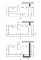
- Manufacturing method> 10 and 11 are diagrams illustrating an example of a manufacturing process of the solid-state imaging device according to the embodiment of the present technology.
- a photodiode 42 for detecting ultraviolet light and a storage section 44 thereof are formed on the back surface side of the semiconductor substrate 40 as shown in FIG. Further, a pinning region 45 penetrating the semiconductor substrate 40 is formed.
- a photodiode 41 for detecting visible light and a storage part 43 thereof are formed on the back side of the semiconductor substrate 40. Then, the transfer gate 13 that transfers the electric charge from the photodiode 41 to the storage unit 43 is formed.
- a conductor 46 is formed on the front side of the semiconductor substrate 40 and connected to the wiring 47. Further, a through hole 38 is formed at the position of the conductor 46 from the back surface side of the semiconductor substrate 40 by dry etching or the like.
- a fixed charge film 39 is formed on the back surface side of the semiconductor substrate 40 including the through hole 38.
- the insulating film 30 is stacked on the fixed charge film 39 to fill the through hole 38.
- a through-hole is formed in the central portion of the insulating film 30 filled in the through-hole 38 until reaching the conductor 46 on the front side, and the conductor 46 is formed in this through-hole. Embed. Then, the conductor 46 is connected to the storage unit 44.
- the storage section 44 on the back side and the wiring 47 on the front side are connected via the conductor 46. Thereby, the electric charge of the ultraviolet light accumulated in the accumulation section 44 on the back side is transferred to the circuit on the front side and output as an ultraviolet light signal.
- the solid-state imaging device has been described in detail. However, this embodiment may be applied to an electronic device equipped with the solid-state imaging device.
- the processing procedure described in the above-described embodiment may be regarded as a method having these series of procedures, or a program for causing a computer to execute these series of procedures or a recording medium storing the program. May be caught.
- a recording medium for example, a CD (Compact Disc), an MD (MiniDisc), a DVD (Digital Versatile Disc), a memory card, a Blu-ray Disc (Blu-ray (registered trademark) Disc), or the like can be used.
- the present technology may have the following configurations.
- the substrate is a silicon substrate
- the first photoelectric conversion element is formed in a surface region of the other surface of the substrate.
- the connection unit is a conductor penetrating the substrate.
- the solid-state imaging device according to any one of (1) to (7), further including a potential barrier between the first storage unit and the second storage unit.
- the first photoelectric conversion element photoelectrically converts light of a plurality of colors different from each other;
- the solid-state imaging device according to any one of (1) to (8), wherein the first accumulation unit accumulates the photoelectrically converted charges for each color in a penetrating direction of the substrate.
- the second photoelectric conversion element is divided into left and right and performs photoelectric conversion respectively,
- the solid-state imaging device according to any one of (1) to (9), wherein the second storage unit is configured to store charge by being divided corresponding to each of the left and right second photoelectric conversion elements. element.
- the solid-state imaging device A first photoelectric conversion element; A first accumulation unit that accumulates charges photoelectrically converted by the first photoelectric conversion element; A second photoelectric conversion element; A second storage unit that is disposed on one surface of the substrate and stores the charge photoelectrically converted by the second photoelectric conversion element; A connection unit connected to the second storage unit and transferring the charge stored in the second storage unit to the other surface of the substrate.
Landscapes
- Engineering & Computer Science (AREA)
- Multimedia (AREA)
- Signal Processing (AREA)
- Solid State Image Pick-Up Elements (AREA)
- Transforming Light Signals Into Electric Signals (AREA)
Abstract
可視光および紫外光を1つの画素内で検出する固体撮像素子において解像度を向上させる。 第1および第2の光電変換素子は、入射された光についてそれぞれ光電変換を行う。第1の蓄積部は、第1の光電変換素子により光電変換された電荷を蓄積する。第2の蓄積部は、基板の一方の面に配されて、第2の光電変換素子により光電変換された電荷を蓄積する。接続部は、第2の蓄積部に接続して、第2の蓄積部に蓄積された電荷を基板の他方の面に転送する。
Description
本技術は、固体撮像素子に関する。詳しくは、被写体からの光を光電変換する固体撮像素子、および、電子装置に関する。
固体撮像素子において、可視光だけでなく紫外光についても検出する機能を備えるものが知られている。例えば、SOI(Silicon On Insulator)構造の半導体基板に、紫外線感光素子と可視光感光素子とを形成して、1チップ化する技術が提案されている(例えば、特許文献1参照。)。
上述の従来技術では、シリコン基板上に可視光感光素子および紫外線感光素子の両者を形成している。しかしながら、この従来技術では、紫外光と可視光のそれぞれを検出するために、それぞれの光検出領域を平面的に別々に割り当てる構造であるため、解像度の低下を招くという問題がある。また、ベイヤ配列が不可能な構成となるため、解像感の低下に加えて、色補間処理が困難になるという問題がある。
本技術はこのような状況に鑑みて生み出されたものであり、可視光および紫外光を検出する固体撮像素子において解像度を向上させることを目的とする。
本技術は、上述の問題点を解消するためになされたものであり、その第1の側面は、第1の光電変換素子と、上記第1の光電変換素子により光電変換された電荷を蓄積する第1の蓄積部と、第2の光電変換素子と、基板の一方の面に配されて上記第2の光電変換素子により光電変換された電荷を蓄積する第2の蓄積部と、上記第2の蓄積部に接続して上記第2の蓄積部に蓄積された電荷を上記基板の他方の面に転送する接続部とを具備する固体撮像素子および電子装置である。これにより、基板の両面において個別に光電変換を行うという作用をもたらす。
また、この第1の側面において、上記基板の一方の面から光が入射され、上記第1の光電変換素子は、可視光領域の光を光電変換し、上記第2の光電変換素子は、紫外光領域の光を光電変換するようにしてもよい。これにより、可視光と紫外光とを1つの画素において光電変換するという作用をもたらす。
また、この第1の側面において、上記基板はシリコン基板であり、上記第2の光電変換素子は、上記基板の一方の面の表面から40ナノメートルまでの深さの領域に形成されるようにしてもよい。この場合において、上記第1の光電変換素子は、上記基板の他方の面の表面の領域に形成される。
また、この第1の側面において、上記接続部は、上記基板を貫通する導電体であってもよい。これにより、第2の蓄積部に蓄積された電荷を、基板を貫通して他方の面に転送するという作用をもたらす。なお、この導電体は、少なくともタングステンを含んで形成されてもよい。
また、この第1の側面において、上記第2の蓄積部の表面にハフニウム膜をさらに具備してもよい。これにより、反射を防止し、暗電流を抑制するという作用をもたらす。
また、この第1の側面において、上記第1の蓄積部と上記第2の蓄積部との間にポテンシャル障壁をさらに具備してもよい。これにより、異なる波長の光の電荷を切り分けるという作用をもたらす。
また、この第1の側面において、上記第1の光電変換素子は、互いに異なる複数の色の光を光電変換し、上記第1の蓄積部は、上記光電変換された電荷を上記基板の貫通方向において色毎に蓄積するようにしてもよい。これにより、色別カラーフィルタを不要にするという作用をもたらす。
また、この第1の側面において、上記第2の光電変換素子は、左右に分割されてそれぞれ光電変換を行い、上記第2の蓄積部は、左右に分割された上記第2の光電変換素子の各々に対応して分割されて電荷を蓄積するようにしてもよい。これにより、左右に分割された第2の光電変換素子による電荷に基づいて位相差を検出してオートフォーカスを行うという作用をもたらす。
以下、本技術を実施するための形態(以下、実施の形態と称する)について説明する。説明は以下の順序により行う。
1.第1の実施の形態(裏面側に紫外光検出用フォトダイオードを設けた例)
2.第2の実施の形態(裏面側の表面にハフニウム膜を堆積させた例)
3.第3の実施の形態(紫外光検出用フォトダイオードの直下にポテンシャル障壁を設けた例)
4.第4の実施の形態(可視光検出用フォトダイオードをシリコン内縦分光構造とした例)
5.第5の実施の形態(紫外光信号を利用して位相差検出を行う例)
6.製造方法
1.第1の実施の形態(裏面側に紫外光検出用フォトダイオードを設けた例)
2.第2の実施の形態(裏面側の表面にハフニウム膜を堆積させた例)
3.第3の実施の形態(紫外光検出用フォトダイオードの直下にポテンシャル障壁を設けた例)
4.第4の実施の形態(可視光検出用フォトダイオードをシリコン内縦分光構造とした例)
5.第5の実施の形態(紫外光信号を利用して位相差検出を行う例)
6.製造方法
<1.第1の実施の形態>
[固体撮像素子]
図1は、本技術の第1の実施の形態における固体撮像素子の1つの画素の断面の概要例を示す図である。
[固体撮像素子]
図1は、本技術の第1の実施の形態における固体撮像素子の1つの画素の断面の概要例を示す図である。
ここでは、一例として、裏面照射型の固体撮像素子を想定する。すなわち、被写体からの光は裏面側(図における下側)から入射する。この固体撮像素子には、半導体基板40上に裏面側から、オンチップレンズ10、カラーフィルタ20、および、絶縁膜30が形成される。カラーフィルタ20の色は、紫外光および可視光領域を透過するものであればよい。例えば、クリア(白色)フィルタであってもよく、また、緑色、赤色、青色、補色などであってもよい。
これらを介して半導体基板40の裏面から入射した入射光は、半導体基板40内のフォトダイオード(Photo Diode:PD)によって受光される。フォトダイオードは入射光に応じた電荷を発生する。半導体基板40は、表面側に可視光を光電変換するフォトダイオード41を備え、裏面側に紫外光を光電変換するフォトダイオード42を備える。フォトダイオード41および42は、P-型のウェル49により緩やかに分離される。特に波長400nm(青色)以降の光電荷は、このポテンシャル勾配によりフォトダイオード41へと移動する。なお、フォトダイオード41は、特許請求の範囲に記載の第1の光電変換素子の一例であり、フォトダイオード42は、特許請求の範囲に記載の第2の光電変換素子の一例である。
半導体基板40は、例えば、P型シリコン基板である。フォトダイオード41は、P型シリコン基板に形成されたN+領域と、そのN+領域に拡散または埋込みにより形成されたP++領域とを備える。フォトダイオード41によって光電変換された電荷は、転送ゲート13によって蓄積部43に転送され、蓄積される。この蓄積部43は、N++領域として形成される。なお、蓄積部43は、特許請求の範囲に記載の第1の蓄積部の一例である。
また、フォトダイオード42は、P型シリコン基板に形成されたN-領域を備える。フォトダイオード42によって光電変換された電荷は、蓄積部44に蓄積される。この蓄積部44は、N++領域として形成される。なお、蓄積部44は、特許請求の範囲に記載の第2の蓄積部の一例である。
ここで、波長400nmまでの紫外光のシリコンに対する吸収率は、シリコンの深さ0乃至40nmの領域で略100%となる。したがって、裏面側に配される紫外光検出用のフォトダイオード42は、空乏化する領域が半導体基板40の裏面側から深さ40nm程度までの領域にあることが好ましい。
蓄積部44に蓄積された電荷は、導電体46を介して表面側の配線47に転送される。導電体46は、蓄積部44に接続して半導体基板40を貫通する導電性の部材である。この導電体46は、暗電流防止のためのピニング領域45(P++)に囲まれた貫通電極の中心部分に形成される。この導電体46としては、例えば、タングステン(W)などの金属材料を採用することができる。なお、導電体46は、特許請求の範囲に記載の接続部の一例である。
このような構造により、1つの画素において、半導体基板40の裏面側に配されるフォトダイオード42により紫外光を検出し、表面側に配されるフォトダイオード41により可視光を検出することができる。そして、光電変換された電荷は、転送ゲート13および導電体46を介して、半導体基板40の表面側の回路に転送される。
[等価回路]
図2は、本技術の第1の実施の形態における固体撮像素子の1つの画素の等価回路の例を示す図である。
図2は、本技術の第1の実施の形態における固体撮像素子の1つの画素の等価回路の例を示す図である。
この画素は、可視光フォトダイオード110と、紫外光フォトダイオード120と、転送トランジスタ130と、リセットトランジスタ140と、増幅トランジスタ151および152と、選択トランジスタ161および162とを備える。
また、画素に対して、行方向に転送信号線TRX、リセット信号線RSTおよび選択信号線SELの3本の信号線が設けられ、列方向に可視光の垂直信号線191および紫外光の垂直信号線192が設けられる。また、リセットトランジスタ140および増幅トランジスタ151および152のドレイン側には電源電圧Vddが供給される。
可視光フォトダイオード110は上述のフォトダイオード41に対応するものであり、紫外光フォトダイオード120は上述のフォトダイオード42に対応するものである。これらフォトダイオード110および120のアノードは接地される。
転送トランジスタ130は、可視光フォトダイオード110において光電変換された電荷を転送するトランジスタである。この転送トランジスタ130は、可視光フォトダイオード110のカソードと、フローティングディフュージョン領域FD(Floating Diffusion)との間に設けられる。この転送トランジスタ130は、そのゲートに垂直駆動回路から転送信号線を介してハイレベルの信号が入力された際にオン状態となり、可視光フォトダイオード110において光電変換された電荷をフローティングディフュージョン領域FDに転送する。
フローティングディフュージョン領域FDは、光電変換された電荷を電圧信号に変換する拡散層領域である。このフローティングディフュージョン領域FDの電圧信号は、リセットトランジスタ140のドレインおよび増幅トランジスタ151および152のゲートに接続される。フローティングディフュージョン領域FDは、上述の蓄積部43および44に対応するものである。
リセットトランジスタ140は、フローティングディフュージョン領域FDの電圧をリセットするためのトランジスタである。このリセットトランジスタ140は、電源電圧Vddとフローティングディフュージョン領域FDとの間に設けられる。このリセットトランジスタ140は、そのゲートに垂直駆動回路からリセット信号線にハイレベルの信号が入力された際にオン状態となり、フローティングディフュージョン領域FDの電位を電源電圧Vddにリセットする。
増幅トランジスタ151および152は、フローティングディフュージョン領域FDの電圧信号を増幅するトランジスタである。この増幅トランジスタ151および152は、フローティングディフュージョン領域FDの電圧信号を増幅し、その増幅信号を画素信号として、それぞれ選択トランジスタ161および162に出力する。
選択トランジスタ161および162は、この画素を選択するためのトランジスタである。この選択トランジスタ161および162は、増幅トランジスタ151および152と垂直信号線191および192との間に設けられる。この選択トランジスタ161および162は、そのゲートに垂直駆動回路から選択信号線にハイレベルの信号が入力された際にオン状態となり、増幅トランジスタ151および152で増幅された電圧信号を、対応する垂直信号線191および192に出力する。
[動作]
図3は、本技術の第1の実施の形態における固体撮像素子の動作タイミングの一例を示す図である。
図3は、本技術の第1の実施の形態における固体撮像素子の動作タイミングの一例を示す図である。
まず、リセット信号線RSTおよび転送信号線TRXがアサートされ、これにより可視光フォトダイオード110および紫外光フォトダイオード120の電荷がリセットされる。
露光中に光電変換された電荷は、可視光フォトダイオード110および紫外光フォトダイオード120にそれぞれ蓄積される。可視光フォトダイオード110にはシリコン吸収率に従って可視光領域の光が蓄積され、紫外光フォトダイオード120には紫外光領域の光が蓄積される。
そして、露光期間が経過すると、選択信号線SELがアサートされ、画素が選択される。これにより、最初に紫外光フォトダイオード120に蓄積された紫外光の電荷が増幅トランジスタ152に供給され、紫外光信号が垂直信号線192に出力される。
その後、リセット信号線RSTがアサートされ、これにより可視光および紫外光がリセットされ、続いて可視光フォトダイオード110によって可視光が検出される。そして、転送信号線TRXがアサートされると、可視光の電荷が増幅トランジスタ151に供給され、可視光信号が垂直信号線191に出力される。
このように、本技術の第1の実施の形態によれば、1つの画素において、半導体基板40の裏面側に配されるフォトダイオード42により紫外光を検出し、表面側に配されるフォトダイオード41により可視光を検出することができる。裏面側に配されるフォトダイオード42により光電変換された紫外光の電荷は、導電体46を介して半導体基板40の表面側の回路に効率良く転送される。
すなわち、従来技術のように、可視光と紫外光のそれぞれの光検出領域を平面的に別々に割り当てる構成ではなく、1つの画素で両方の光を検出することができる。これにより解像度を低下させることなく、紫外光から可視光までの信号の検出が可能になる。
また、一般に、撮像用またはセンシング用途において可視光信号は信号対雑音性能(SN比)が最重要視される。この点、この実施の形態では、可視光の信号検出は、表面をP型で覆って埋込み構造としたHAD(Hole-Accumulation Diode)構造を採用するとともに、転送型構造を採用した。これにより、高いSN比を維持することができる。
一方、紫外光信号の主な用途を鑑みると、必ずしも高いSN比を必要としないため、HAD構造および転送型とする必要がない。さらに、シリコン表面をHAD構造にしてしまうと、最表面で生成された電荷が他のノードへ拡散し、信号電荷として寄与できないおそれがある。これに対し、この実施の形態では、紫外光についてはHAD構造を採用せず、最表面から蓄積部を設けているため、信号電荷を逃すことがなく紫外光信号を検出することが可能となる。
なお、縦型転送ゲート(VTG:Vertical Transfer Gate)により深部の蓄積層の電荷を転送するのは、一般に困難であると考えられる。したがって、この実施の形態のように、裏面の蓄積層を裏面側から直結して信号検出することが好適である。
<2.第2の実施の形態>
図4は、本技術の第2の実施の形態における固体撮像素子の1つの画素の断面の概要例を示す図である。
図4は、本技術の第2の実施の形態における固体撮像素子の1つの画素の断面の概要例を示す図である。
この第2の実施の形態における固体撮像素子は、上述の第1の実施の形態と同様に、半導体基板40の表面側に可視光を検出するためのフォトダイオード41が配され、裏面側に紫外光を検出するためのフォトダイオード42が配される。そして、半導体基板40の裏面側の表面においてハフニウム膜35が堆積される。このハフニウム膜35は、マイナスに帯電しており、表面の欠陥を抑えるものである。これにより、反射を防止し、暗電流を抑制することができる。
なお、ハフニウム膜35以外の構造は、上述の第1の実施の形態と同様である。また、等価回路についても上述の第1の実施の形態と同様である。
このように、本技術の第2の実施の形態によれば、半導体基板40の裏面側の表面にハフニウム膜35を堆積することにより、裏面側における反射を防止し、暗電流を抑制することができる。
<3.第3の実施の形態>
図5は、本技術の第3の実施の形態における固体撮像素子の1つの画素の断面の概要例を示す図である。
図5は、本技術の第3の実施の形態における固体撮像素子の1つの画素の断面の概要例を示す図である。
この第3の実施の形態における固体撮像素子は、上述の第1の実施の形態と同様に、半導体基板40の表面側に可視光を検出するためのフォトダイオード41が配され、裏面側に紫外光を検出するためのフォトダイオード42が配される。そして、フォトダイオード42の直下に高濃度P型層48が配される。この高濃度P型層48は、空乏層が広がらないようにするポテンシャル障壁(電位障壁)として機能する。これにより、紫外光と青色光の電荷を容易に切り分けることができる。
なお、高濃度P型層48以外の構造は、上述の第1の実施の形態と同様である。また、等価回路についても上述の第1の実施の形態と同様である。
このように、本技術の第3の実施の形態によれば、フォトダイオード42の直下にポテンシャル障壁となる高濃度P型層48を配することにより、紫外光と青色光の電荷を容易に切り分けることができる。
<4.第4の実施の形態>
[固体撮像素子]
図6は、本技術の第4の実施の形態における固体撮像素子の1つの画素の断面の概要例を示す図である。
[固体撮像素子]
図6は、本技術の第4の実施の形態における固体撮像素子の1つの画素の断面の概要例を示す図である。
この第4の実施の形態における固体撮像素子は、上述の第1の実施の形態と同様に、裏面側に紫外光を検出するためのフォトダイオード42が配される。一方、可視光を検出するためのフォトダイオード41は、色毎に3分割されている。すなわち、半導体基板40の表面側から順に、赤色、緑色および青色のフォトダイオード41が深さ方向に同軸上に並んで配される、シリコン内縦分光構造を備える。そして、各色の信号電荷の転送のために、縦型転送トランジスタが用いられる。
この場合、全ての色を取り込むために、ホワイトフィルタ21が用いられる。これにより、色別カラーフィルタを配することによる紫外光透過率の影響を気にすることなく、紫外光検出率をより向上させることができる。
[等価回路]
図7は、本技術の第4の実施の形態における固体撮像素子の1つの画素の等価回路の例を示す図である。
図7は、本技術の第4の実施の形態における固体撮像素子の1つの画素の等価回路の例を示す図である。
この第4の実施の形態における固体撮像素子は、上述の第1の実施の形態と異なり、色毎にフォトダイオード111乃至113および転送トランジスタ131乃至133を備える。
転送信号線TRX1乃至TRX3を順次アサートすることにより、赤色、緑色および青色の電荷を増幅トランジスタ151に供給させて、赤色信号、緑色信号および青色信号を得ることができる。
このように、本技術の第4の実施の形態によれば、可視光を検出するためのフォトダイオード41を色毎に分割することにより、色別カラーフィルタを配することによる紫外光透過率の影響を気にすることなく、紫外光検出率をより向上させることができる。
<5.第5の実施の形態>
[固体撮像素子]
図8は、本技術の第5の実施の形態における固体撮像素子の1つの画素の断面の概要例を示す図である。
[固体撮像素子]
図8は、本技術の第5の実施の形態における固体撮像素子の1つの画素の断面の概要例を示す図である。
この第5の実施の形態における固体撮像素子は、上述の第1の実施の形態と異なり、紫外光を検出するためのフォトダイオード42が左右2つに分割され、オートフォーカスの位相差検出用の画素を構成する。
従来の位相差検出画素は、可視光領域を2つに分割するため、可視光の感度を低下させる原因となっていた。上述のように、可視光信号は撮像用またはセンシング用途においてSN比が最重要視される。この点、この第5の実施の形態では、位相差検出に紫外光信号を利用するため、可視光信号における感度低下を防ぐことができる。
左右に分割されたフォトダイオード42の蓄積部44には、それぞれ導電体46が接続されており、蓄積部44に蓄積される電荷は導電体46を介して表面側の配線47にそれぞれ転送される。
[等価回路]
図9は、本技術の第5の実施の形態における固体撮像素子の1つの画素の等価回路の例を示す図である。
図9は、本技術の第5の実施の形態における固体撮像素子の1つの画素の等価回路の例を示す図である。
この第5の実施の形態における固体撮像素子は、上述の第1の実施の形態と異なり、紫外光を検出するフォトダイオードは左右の位相差に合わせて2つのフォトダイオード121および122に分割される。フォトダイオード121および122の出力は、増幅トランジスタ158および159のゲートに接続される。増幅トランジスタ158および159によって増幅された画素信号は、それぞれ選択トランジスタ168および169に出力される。
選択信号線SEL1は選択トランジスタ161および168に共有され、紫外光信号の一方および可視光信号は、共通して制御される。これに対し、選択信号線SEL2は選択トランジスタ169に接続され、紫外光信号の他方は紫外光信号の一方とは独立して制御される。
このように、本技術の第5の実施の形態によれば、紫外光信号を利用して位相差検出を行うことにより、可視光信号における感度低下を防ぐことができる。
<6.製造方法>
図10および図11は、本技術の実施の形態における固体撮像素子の製造工程の例を示す図である。
図10および図11は、本技術の実施の形態における固体撮像素子の製造工程の例を示す図である。
まず、同図におけるaに示されるように、半導体基板40の裏面側に紫外光検出用のフォトダイオード42およびその蓄積部44を形成する。また、半導体基板40を貫通するピニング領域45を形成する。
次に、同図におけるbに示されるように、半導体基板40の裏面側に可視光検出用のフォトダイオード41およびその蓄積部43を形成する。そして、フォトダイオード41から蓄積部43に電荷を転送する転送ゲート13を形成する。
次に、同図におけるcに示されるように、半導体基板40の表面側に導電体46を形成して配線47に接続する。また、導電体46の位置に、半導体基板40の裏面側から貫通孔38をドライエッチング等により形成する。
次に、同図におけるdに示されるように、貫通孔38を含む半導体基板40の裏面側に固定電荷膜39を形成する。
次に、同図におけるeに示されるように、固定電荷膜39の上に絶縁膜30を積層して貫通孔38を充填する。
次に、同図におけるfに示されるように、貫通孔38に充填した絶縁膜30の中心部分に表面側の導電体46に到達するまで貫通孔を形成し、この貫通孔に導電体46を埋め込む。そして、この導電体46を蓄積部44に接続する。
このような製造工程により、導電体46を介して裏面側の蓄積部44と表面側の配線47とが接続される。これにより、裏面側の蓄積部44に蓄積された紫外光の電荷が表面側の回路に転送されて、紫外光信号として出力される。
なお、上述の実施の形態では固体撮像素子について詳細に説明したが、この実施の形態は固体撮像素子が搭載された電子装置に適用してもよい。
なお、上述の実施の形態は本技術を具現化するための一例を示したものであり、実施の形態における事項と、特許請求の範囲における発明特定事項とはそれぞれ対応関係を有する。同様に、特許請求の範囲における発明特定事項と、これと同一名称を付した本技術の実施の形態における事項とはそれぞれ対応関係を有する。ただし、本技術は実施の形態に限定されるものではなく、その要旨を逸脱しない範囲において実施の形態に種々の変形を施すことにより具現化することができる。
また、上述の実施の形態において説明した処理手順は、これら一連の手順を有する方法として捉えてもよく、また、これら一連の手順をコンピュータに実行させるためのプログラム乃至そのプログラムを記憶する記録媒体として捉えてもよい。この記録媒体として、例えば、CD(Compact Disc)、MD(MiniDisc)、DVD(Digital Versatile Disc)、メモリカード、ブルーレイディスク(Blu-ray(登録商標)Disc)等を用いることができる。
なお、本明細書に記載された効果はあくまで例示であって、限定されるものではなく、また、他の効果があってもよい。
なお、本技術は以下のような構成もとることができる。
(1)第1の光電変換素子と、
前記第1の光電変換素子により光電変換された電荷を蓄積する第1の蓄積部と、
第2の光電変換素子と、
基板の一方の面に配されて前記第2の光電変換素子により光電変換された電荷を蓄積する第2の蓄積部と、
前記第2の蓄積部に接続して前記第2の蓄積部に蓄積された電荷を前記基板の他方の面に転送する接続部と
を具備する固体撮像素子。
(2)前記基板の前記一方の面から光が入射され、
前記第1の光電変換素子は、可視光領域の光を光電変換し、
前記第2の光電変換素子は、紫外光領域の光を光電変換する
前記(1)に記載の固体撮像素子。
(3)前記基板はシリコン基板であり、
前記第2の光電変換素子は、前記基板の前記一方の面の表面から40ナノメートルまでの深さの領域に形成される
前記(1)または(2)に記載の固体撮像素子。
(4)前記第1の光電変換素子は、前記基板の前記他方の面の表面の領域に形成される
前記(3)に記載の固体撮像素子。
(5)前記接続部は、前記基板を貫通する導電体である
前記(1)から(4)のいずれかに記載の固体撮像素子。
(6)前記導電体は、少なくともタングステンを含んで形成される
前記(5)に記載の固体撮像素子。
(7)前記第2の蓄積部の表面にハフニウム膜をさらに具備する前記(1)から(6)のいずれかに記載の固体撮像素子。
(8)前記第1の蓄積部と前記第2の蓄積部との間にポテンシャル障壁をさらに具備する前記(1)から(7)のいずれかに記載の固体撮像素子。
(9)前記第1の光電変換素子は、互いに異なる複数の色の光を光電変換し、
前記第1の蓄積部は、前記光電変換された電荷を前記基板の貫通方向において色毎に蓄積する
前記(1)から(8)のいずれかに記載の固体撮像素子。
(10)前記第2の光電変換素子は、左右に分割されてそれぞれ光電変換を行い、
前記第2の蓄積部は、前記左右に分割された前記第2の光電変換素子の各々に対応して分割されて電荷を蓄積する
前記(1)から(9)のいずれかに記載の固体撮像素子。
(11)固体撮像素子が搭載された電子装置において、
前記固体撮像素子は、
第1の光電変換素子と、
前記第1の光電変換素子により光電変換された電荷を蓄積する第1の蓄積部と、
第2の光電変換素子と、
基板の一方の面に配されて前記第2の光電変換素子により光電変換された電荷を蓄積する第2の蓄積部と、
前記第2の蓄積部に接続して前記第2の蓄積部に蓄積された電荷を前記基板の他方の面に転送する接続部と
を備える
電子装置。
(1)第1の光電変換素子と、
前記第1の光電変換素子により光電変換された電荷を蓄積する第1の蓄積部と、
第2の光電変換素子と、
基板の一方の面に配されて前記第2の光電変換素子により光電変換された電荷を蓄積する第2の蓄積部と、
前記第2の蓄積部に接続して前記第2の蓄積部に蓄積された電荷を前記基板の他方の面に転送する接続部と
を具備する固体撮像素子。
(2)前記基板の前記一方の面から光が入射され、
前記第1の光電変換素子は、可視光領域の光を光電変換し、
前記第2の光電変換素子は、紫外光領域の光を光電変換する
前記(1)に記載の固体撮像素子。
(3)前記基板はシリコン基板であり、
前記第2の光電変換素子は、前記基板の前記一方の面の表面から40ナノメートルまでの深さの領域に形成される
前記(1)または(2)に記載の固体撮像素子。
(4)前記第1の光電変換素子は、前記基板の前記他方の面の表面の領域に形成される
前記(3)に記載の固体撮像素子。
(5)前記接続部は、前記基板を貫通する導電体である
前記(1)から(4)のいずれかに記載の固体撮像素子。
(6)前記導電体は、少なくともタングステンを含んで形成される
前記(5)に記載の固体撮像素子。
(7)前記第2の蓄積部の表面にハフニウム膜をさらに具備する前記(1)から(6)のいずれかに記載の固体撮像素子。
(8)前記第1の蓄積部と前記第2の蓄積部との間にポテンシャル障壁をさらに具備する前記(1)から(7)のいずれかに記載の固体撮像素子。
(9)前記第1の光電変換素子は、互いに異なる複数の色の光を光電変換し、
前記第1の蓄積部は、前記光電変換された電荷を前記基板の貫通方向において色毎に蓄積する
前記(1)から(8)のいずれかに記載の固体撮像素子。
(10)前記第2の光電変換素子は、左右に分割されてそれぞれ光電変換を行い、
前記第2の蓄積部は、前記左右に分割された前記第2の光電変換素子の各々に対応して分割されて電荷を蓄積する
前記(1)から(9)のいずれかに記載の固体撮像素子。
(11)固体撮像素子が搭載された電子装置において、
前記固体撮像素子は、
第1の光電変換素子と、
前記第1の光電変換素子により光電変換された電荷を蓄積する第1の蓄積部と、
第2の光電変換素子と、
基板の一方の面に配されて前記第2の光電変換素子により光電変換された電荷を蓄積する第2の蓄積部と、
前記第2の蓄積部に接続して前記第2の蓄積部に蓄積された電荷を前記基板の他方の面に転送する接続部と
を備える
電子装置。
10 オンチップレンズ
13 転送ゲート
20 カラーフィルタ
21 ホワイトフィルタ
30 絶縁膜
35 ハフニウム膜
38 貫通孔
39 固定電荷膜
40 半導体基板
41、42 フォトダイオード
43、44 蓄積部
45 ピニング領域
46 導電体
47 配線
48 高濃度P型層
49 ウェル
110、120、121、122 フォトダイオード
130 転送トランジスタ
140 リセットトランジスタ
151、152、158、159 増幅トランジスタ
161、162、168、169 選択トランジスタ
191、192 垂直信号線
13 転送ゲート
20 カラーフィルタ
21 ホワイトフィルタ
30 絶縁膜
35 ハフニウム膜
38 貫通孔
39 固定電荷膜
40 半導体基板
41、42 フォトダイオード
43、44 蓄積部
45 ピニング領域
46 導電体
47 配線
48 高濃度P型層
49 ウェル
110、120、121、122 フォトダイオード
130 転送トランジスタ
140 リセットトランジスタ
151、152、158、159 増幅トランジスタ
161、162、168、169 選択トランジスタ
191、192 垂直信号線
Claims (11)
- 第1の光電変換素子と、
前記第1の光電変換素子により光電変換された電荷を蓄積する第1の蓄積部と、
第2の光電変換素子と、
基板の一方の面に配されて前記第2の光電変換素子により光電変換された電荷を蓄積する第2の蓄積部と、
前記第2の蓄積部に接続して前記第2の蓄積部に蓄積された電荷を前記基板の他方の面に転送する接続部と
を具備する固体撮像素子。 - 前記基板の前記一方の面から光が入射され、
前記第1の光電変換素子は、可視光領域の光を光電変換し、
前記第2の光電変換素子は、紫外光領域の光を光電変換する
請求項1記載の固体撮像素子。 - 前記基板はシリコン基板であり、
前記第2の光電変換素子は、前記基板の前記一方の面の表面から40ナノメートルまでの深さの領域に形成される
請求項1記載の固体撮像素子。 - 前記第1の光電変換素子は、前記基板の前記他方の面の表面の領域に形成される
請求項3記載の固体撮像素子。 - 前記接続部は、前記基板を貫通する導電体である
請求項1記載の固体撮像素子。 - 前記導電体は、少なくともタングステンを含んで形成される
請求項5記載の固体撮像素子。 - 前記第2の蓄積部の表面にハフニウム膜をさらに具備する請求項1記載の固体撮像素子。
- 前記第1の蓄積部と前記第2の蓄積部との間にポテンシャル障壁をさらに具備する請求項1記載の固体撮像素子。
- 前記第1の光電変換素子は、互いに異なる複数の色の光を光電変換し、
前記第1の蓄積部は、前記光電変換された電荷を前記基板の貫通方向において色毎に蓄積する
請求項1記載の固体撮像素子。 - 前記第2の光電変換素子は、左右に分割されてそれぞれ光電変換を行い、
前記第2の蓄積部は、前記左右に分割された前記第2の光電変換素子の各々に対応して分割されて電荷を蓄積する
請求項1記載の固体撮像素子。 - 固体撮像素子が搭載された電子装置において、
前記固体撮像素子は、
第1の光電変換素子と、
前記第1の光電変換素子により光電変換された電荷を蓄積する第1の蓄積部と、
第2の光電変換素子と、
基板の一方の面に配されて前記第2の光電変換素子により光電変換された電荷を蓄積する第2の蓄積部と、
前記第2の蓄積部に接続して前記第2の蓄積部に蓄積された電荷を前記基板の他方の面に転送する接続部と
を備える
電子装置。
Priority Applications (1)
| Application Number | Priority Date | Filing Date | Title |
|---|---|---|---|
| US17/250,708 US11855108B2 (en) | 2018-09-04 | 2019-09-02 | Solid-state imaging element and electronic device |
Applications Claiming Priority (2)
| Application Number | Priority Date | Filing Date | Title |
|---|---|---|---|
| JP2018165458A JP2020038910A (ja) | 2018-09-04 | 2018-09-04 | 固体撮像素子および電子装置 |
| JP2018-165458 | 2018-09-04 |
Publications (1)
| Publication Number | Publication Date |
|---|---|
| WO2020050195A1 true WO2020050195A1 (ja) | 2020-03-12 |
Family
ID=69721643
Family Applications (1)
| Application Number | Title | Priority Date | Filing Date |
|---|---|---|---|
| PCT/JP2019/034348 Ceased WO2020050195A1 (ja) | 2018-09-04 | 2019-09-02 | 固体撮像素子および電子装置 |
Country Status (3)
| Country | Link |
|---|---|
| US (1) | US11855108B2 (ja) |
| JP (1) | JP2020038910A (ja) |
| WO (1) | WO2020050195A1 (ja) |
Cited By (1)
| Publication number | Priority date | Publication date | Assignee | Title |
|---|---|---|---|---|
| WO2026074912A1 (ja) * | 2024-10-01 | 2026-04-09 | ソニーセミコンダクタソリューションズ株式会社 | 光検出装置および電子機器 |
Families Citing this family (1)
| Publication number | Priority date | Publication date | Assignee | Title |
|---|---|---|---|---|
| JP2023174229A (ja) * | 2022-05-27 | 2023-12-07 | キヤノン株式会社 | 光電変換装置 |
Citations (5)
| Publication number | Priority date | Publication date | Assignee | Title |
|---|---|---|---|---|
| JP2009135314A (ja) * | 2007-11-30 | 2009-06-18 | Oki Semiconductor Co Ltd | フォトダイオードの製造方法およびそれを用いて形成されたフォトダイオード |
| JP2015038931A (ja) * | 2013-08-19 | 2015-02-26 | ソニー株式会社 | 固体撮像素子および電子機器 |
| WO2015151651A1 (ja) * | 2014-04-04 | 2015-10-08 | シャープ株式会社 | 受光器及び携帯型電子機器 |
| WO2016147837A1 (ja) * | 2015-03-13 | 2016-09-22 | ソニー株式会社 | 固体撮像素子、駆動方法、および電子機器 |
| WO2017138197A1 (ja) * | 2016-02-09 | 2017-08-17 | ソニー株式会社 | 半導体装置及び半導体装置の製造方法、並びに、固体撮像素子及び電子機器 |
Family Cites Families (2)
| Publication number | Priority date | Publication date | Assignee | Title |
|---|---|---|---|---|
| JP2009170615A (ja) | 2008-01-15 | 2009-07-30 | Oki Semiconductor Co Ltd | 光センサおよびそれを備えたフォトic |
| US10805567B2 (en) * | 2018-09-13 | 2020-10-13 | Semiconductor Components Industries, Llc | Imaging pixels with non-destructive readout capabilities |
-
2018
- 2018-09-04 JP JP2018165458A patent/JP2020038910A/ja active Pending
-
2019
- 2019-09-02 US US17/250,708 patent/US11855108B2/en active Active
- 2019-09-02 WO PCT/JP2019/034348 patent/WO2020050195A1/ja not_active Ceased
Patent Citations (5)
| Publication number | Priority date | Publication date | Assignee | Title |
|---|---|---|---|---|
| JP2009135314A (ja) * | 2007-11-30 | 2009-06-18 | Oki Semiconductor Co Ltd | フォトダイオードの製造方法およびそれを用いて形成されたフォトダイオード |
| JP2015038931A (ja) * | 2013-08-19 | 2015-02-26 | ソニー株式会社 | 固体撮像素子および電子機器 |
| WO2015151651A1 (ja) * | 2014-04-04 | 2015-10-08 | シャープ株式会社 | 受光器及び携帯型電子機器 |
| WO2016147837A1 (ja) * | 2015-03-13 | 2016-09-22 | ソニー株式会社 | 固体撮像素子、駆動方法、および電子機器 |
| WO2017138197A1 (ja) * | 2016-02-09 | 2017-08-17 | ソニー株式会社 | 半導体装置及び半導体装置の製造方法、並びに、固体撮像素子及び電子機器 |
Cited By (1)
| Publication number | Priority date | Publication date | Assignee | Title |
|---|---|---|---|---|
| WO2026074912A1 (ja) * | 2024-10-01 | 2026-04-09 | ソニーセミコンダクタソリューションズ株式会社 | 光検出装置および電子機器 |
Also Published As
| Publication number | Publication date |
|---|---|
| US11855108B2 (en) | 2023-12-26 |
| JP2020038910A (ja) | 2020-03-12 |
| US20210202545A1 (en) | 2021-07-01 |
Similar Documents
| Publication | Publication Date | Title |
|---|---|---|
| JP6190392B2 (ja) | 固体撮像素子および電子機器 | |
| CN108111787B (zh) | 摄像器件 | |
| TWI742573B (zh) | 固體攝像元件及其製造方法以及電子機器 | |
| CN106449677B (zh) | 具有混合型异质结构的图像传感器 | |
| EP2980852B1 (en) | Solid-state image sensing element and imaging system | |
| US8101978B2 (en) | Circuit and photo sensor overlap for backside illumination image sensor | |
| US9490282B2 (en) | Photosensitive capacitor pixel for image sensor | |
| JP5269425B2 (ja) | 固体撮像素子および固体撮像装置 | |
| CN102082155B (zh) | 固体摄像器件、相机、半导体器件及其制造方法 | |
| JP2012033583A (ja) | 固体撮像素子及びその製造方法、並びに撮像装置 | |
| JP2008543061A (ja) | グローバルシャッターを有するピン光ダイオード画素 | |
| JP2008294175A (ja) | 固体撮像装置およびカメラ | |
| US20150295007A1 (en) | Image sensor with dielectric charge trapping device | |
| TWI709235B (zh) | 固體攝像元件、其製造方法及電子機器 | |
| WO2018105334A1 (ja) | 固体撮像素子及び電子機器 | |
| CN210168124U (zh) | 图像传感器 | |
| JP5167693B2 (ja) | 固体撮像装置およびカメラ | |
| US11855108B2 (en) | Solid-state imaging element and electronic device | |
| HK1212818B (en) | Image sensor pixel and image sensor |
Legal Events
| Date | Code | Title | Description |
|---|---|---|---|
| 121 | Ep: the epo has been informed by wipo that ep was designated in this application |
Ref document number: 19858263 Country of ref document: EP Kind code of ref document: A1 |
|
| NENP | Non-entry into the national phase |
Ref country code: DE |
|
| 122 | Ep: pct application non-entry in european phase |
Ref document number: 19858263 Country of ref document: EP Kind code of ref document: A1 |