WO2020050131A1 - Conductive roll - Google Patents
Conductive roll Download PDFInfo
- Publication number
- WO2020050131A1 WO2020050131A1 PCT/JP2019/033941 JP2019033941W WO2020050131A1 WO 2020050131 A1 WO2020050131 A1 WO 2020050131A1 JP 2019033941 W JP2019033941 W JP 2019033941W WO 2020050131 A1 WO2020050131 A1 WO 2020050131A1
- Authority
- WO
- WIPO (PCT)
- Prior art keywords
- particles
- rubber
- conductive
- image
- surface layer
- Prior art date
Links
Images

Classifications
-
- G—PHYSICS
- G03—PHOTOGRAPHY; CINEMATOGRAPHY; ANALOGOUS TECHNIQUES USING WAVES OTHER THAN OPTICAL WAVES; ELECTROGRAPHY; HOLOGRAPHY
- G03G—ELECTROGRAPHY; ELECTROPHOTOGRAPHY; MAGNETOGRAPHY
- G03G15/00—Apparatus for electrographic processes using a charge pattern
- G03G15/02—Apparatus for electrographic processes using a charge pattern for laying down a uniform charge, e.g. for sensitising; Corona discharge devices
- G03G15/0208—Apparatus for electrographic processes using a charge pattern for laying down a uniform charge, e.g. for sensitising; Corona discharge devices by contact, friction or induction, e.g. liquid charging apparatus
- G03G15/0216—Apparatus for electrographic processes using a charge pattern for laying down a uniform charge, e.g. for sensitising; Corona discharge devices by contact, friction or induction, e.g. liquid charging apparatus by bringing a charging member into contact with the member to be charged, e.g. roller, brush chargers
- G03G15/0233—Structure, details of the charging member, e.g. chemical composition, surface properties
-
- G—PHYSICS
- G03—PHOTOGRAPHY; CINEMATOGRAPHY; ANALOGOUS TECHNIQUES USING WAVES OTHER THAN OPTICAL WAVES; ELECTROGRAPHY; HOLOGRAPHY
- G03G—ELECTROGRAPHY; ELECTROPHOTOGRAPHY; MAGNETOGRAPHY
- G03G5/00—Recording members for original recording by exposure, e.g. to light, to heat, to electrons; Manufacture thereof; Selection of materials therefor
- G03G5/02—Charge-receiving layers
- G03G5/04—Photoconductive layers; Charge-generation layers or charge-transporting layers; Additives therefor; Binders therefor
-
- B—PERFORMING OPERATIONS; TRANSPORTING
- B32—LAYERED PRODUCTS
- B32B—LAYERED PRODUCTS, i.e. PRODUCTS BUILT-UP OF STRATA OF FLAT OR NON-FLAT, e.g. CELLULAR OR HONEYCOMB, FORM
- B32B1/00—Layered products having a general shape other than plane
-
- B—PERFORMING OPERATIONS; TRANSPORTING
- B32—LAYERED PRODUCTS
- B32B—LAYERED PRODUCTS, i.e. PRODUCTS BUILT-UP OF STRATA OF FLAT OR NON-FLAT, e.g. CELLULAR OR HONEYCOMB, FORM
- B32B1/00—Layered products having a general shape other than plane
- B32B1/08—Tubular products
-
- B—PERFORMING OPERATIONS; TRANSPORTING
- B32—LAYERED PRODUCTS
- B32B—LAYERED PRODUCTS, i.e. PRODUCTS BUILT-UP OF STRATA OF FLAT OR NON-FLAT, e.g. CELLULAR OR HONEYCOMB, FORM
- B32B15/00—Layered products comprising a layer of metal
- B32B15/04—Layered products comprising a layer of metal comprising metal as the main or only constituent of a layer, which is next to another layer of the same or of a different material
- B32B15/06—Layered products comprising a layer of metal comprising metal as the main or only constituent of a layer, which is next to another layer of the same or of a different material of natural rubber or synthetic rubber
-
- B—PERFORMING OPERATIONS; TRANSPORTING
- B32—LAYERED PRODUCTS
- B32B—LAYERED PRODUCTS, i.e. PRODUCTS BUILT-UP OF STRATA OF FLAT OR NON-FLAT, e.g. CELLULAR OR HONEYCOMB, FORM
- B32B15/00—Layered products comprising a layer of metal
- B32B15/18—Layered products comprising a layer of metal comprising iron or steel
-
- B—PERFORMING OPERATIONS; TRANSPORTING
- B32—LAYERED PRODUCTS
- B32B—LAYERED PRODUCTS, i.e. PRODUCTS BUILT-UP OF STRATA OF FLAT OR NON-FLAT, e.g. CELLULAR OR HONEYCOMB, FORM
- B32B25/00—Layered products comprising a layer of natural or synthetic rubber
- B32B25/04—Layered products comprising a layer of natural or synthetic rubber comprising rubber as the main or only constituent of a layer, which is next to another layer of the same or of a different material
- B32B25/042—Layered products comprising a layer of natural or synthetic rubber comprising rubber as the main or only constituent of a layer, which is next to another layer of the same or of a different material of natural rubber or synthetic rubber
-
- B—PERFORMING OPERATIONS; TRANSPORTING
- B32—LAYERED PRODUCTS
- B32B—LAYERED PRODUCTS, i.e. PRODUCTS BUILT-UP OF STRATA OF FLAT OR NON-FLAT, e.g. CELLULAR OR HONEYCOMB, FORM
- B32B25/00—Layered products comprising a layer of natural or synthetic rubber
- B32B25/04—Layered products comprising a layer of natural or synthetic rubber comprising rubber as the main or only constituent of a layer, which is next to another layer of the same or of a different material
- B32B25/08—Layered products comprising a layer of natural or synthetic rubber comprising rubber as the main or only constituent of a layer, which is next to another layer of the same or of a different material of synthetic resin
-
- B—PERFORMING OPERATIONS; TRANSPORTING
- B32—LAYERED PRODUCTS
- B32B—LAYERED PRODUCTS, i.e. PRODUCTS BUILT-UP OF STRATA OF FLAT OR NON-FLAT, e.g. CELLULAR OR HONEYCOMB, FORM
- B32B25/00—Layered products comprising a layer of natural or synthetic rubber
- B32B25/14—Layered products comprising a layer of natural or synthetic rubber comprising synthetic rubber copolymers
-
- B—PERFORMING OPERATIONS; TRANSPORTING
- B32—LAYERED PRODUCTS
- B32B—LAYERED PRODUCTS, i.e. PRODUCTS BUILT-UP OF STRATA OF FLAT OR NON-FLAT, e.g. CELLULAR OR HONEYCOMB, FORM
- B32B27/00—Layered products comprising a layer of synthetic resin
- B32B27/28—Layered products comprising a layer of synthetic resin comprising synthetic resins not wholly covered by any one of the sub-groups B32B27/30 - B32B27/42
- B32B27/281—Layered products comprising a layer of synthetic resin comprising synthetic resins not wholly covered by any one of the sub-groups B32B27/30 - B32B27/42 comprising polyimides
-
- B—PERFORMING OPERATIONS; TRANSPORTING
- B32—LAYERED PRODUCTS
- B32B—LAYERED PRODUCTS, i.e. PRODUCTS BUILT-UP OF STRATA OF FLAT OR NON-FLAT, e.g. CELLULAR OR HONEYCOMB, FORM
- B32B7/00—Layered products characterised by the relation between layers; Layered products characterised by the relative orientation of features between layers, or by the relative values of a measurable parameter between layers, i.e. products comprising layers having different physical, chemical or physicochemical properties; Layered products characterised by the interconnection of layers
- B32B7/04—Interconnection of layers
- B32B7/12—Interconnection of layers using interposed adhesives or interposed materials with bonding properties
-
- B—PERFORMING OPERATIONS; TRANSPORTING
- B32—LAYERED PRODUCTS
- B32B—LAYERED PRODUCTS, i.e. PRODUCTS BUILT-UP OF STRATA OF FLAT OR NON-FLAT, e.g. CELLULAR OR HONEYCOMB, FORM
- B32B2250/00—Layers arrangement
- B32B2250/02—2 layers
-
- B—PERFORMING OPERATIONS; TRANSPORTING
- B32—LAYERED PRODUCTS
- B32B—LAYERED PRODUCTS, i.e. PRODUCTS BUILT-UP OF STRATA OF FLAT OR NON-FLAT, e.g. CELLULAR OR HONEYCOMB, FORM
- B32B2255/00—Coating on the layer surface
- B32B2255/10—Coating on the layer surface on synthetic resin layer or on natural or synthetic rubber layer
-
- B—PERFORMING OPERATIONS; TRANSPORTING
- B32—LAYERED PRODUCTS
- B32B—LAYERED PRODUCTS, i.e. PRODUCTS BUILT-UP OF STRATA OF FLAT OR NON-FLAT, e.g. CELLULAR OR HONEYCOMB, FORM
- B32B2255/00—Coating on the layer surface
- B32B2255/20—Inorganic coating
-
- B—PERFORMING OPERATIONS; TRANSPORTING
- B32—LAYERED PRODUCTS
- B32B—LAYERED PRODUCTS, i.e. PRODUCTS BUILT-UP OF STRATA OF FLAT OR NON-FLAT, e.g. CELLULAR OR HONEYCOMB, FORM
- B32B2255/00—Coating on the layer surface
- B32B2255/26—Polymeric coating
-
- B—PERFORMING OPERATIONS; TRANSPORTING
- B32—LAYERED PRODUCTS
- B32B—LAYERED PRODUCTS, i.e. PRODUCTS BUILT-UP OF STRATA OF FLAT OR NON-FLAT, e.g. CELLULAR OR HONEYCOMB, FORM
- B32B2264/00—Composition or properties of particles which form a particulate layer or are present as additives
- B32B2264/10—Inorganic particles
- B32B2264/105—Metal
-
- B—PERFORMING OPERATIONS; TRANSPORTING
- B32—LAYERED PRODUCTS
- B32B—LAYERED PRODUCTS, i.e. PRODUCTS BUILT-UP OF STRATA OF FLAT OR NON-FLAT, e.g. CELLULAR OR HONEYCOMB, FORM
- B32B2264/00—Composition or properties of particles which form a particulate layer or are present as additives
- B32B2264/10—Inorganic particles
- B32B2264/107—Ceramic
- B32B2264/108—Carbon, e.g. graphite particles
-
- B—PERFORMING OPERATIONS; TRANSPORTING
- B32—LAYERED PRODUCTS
- B32B—LAYERED PRODUCTS, i.e. PRODUCTS BUILT-UP OF STRATA OF FLAT OR NON-FLAT, e.g. CELLULAR OR HONEYCOMB, FORM
- B32B2307/00—Properties of the layers or laminate
- B32B2307/20—Properties of the layers or laminate having particular electrical or magnetic properties, e.g. piezoelectric
- B32B2307/202—Conductive
-
- B—PERFORMING OPERATIONS; TRANSPORTING
- B32—LAYERED PRODUCTS
- B32B—LAYERED PRODUCTS, i.e. PRODUCTS BUILT-UP OF STRATA OF FLAT OR NON-FLAT, e.g. CELLULAR OR HONEYCOMB, FORM
- B32B2307/00—Properties of the layers or laminate
- B32B2307/30—Properties of the layers or laminate having particular thermal properties
- B32B2307/302—Conductive
-
- B—PERFORMING OPERATIONS; TRANSPORTING
- B32—LAYERED PRODUCTS
- B32B—LAYERED PRODUCTS, i.e. PRODUCTS BUILT-UP OF STRATA OF FLAT OR NON-FLAT, e.g. CELLULAR OR HONEYCOMB, FORM
- B32B2307/00—Properties of the layers or laminate
- B32B2307/50—Properties of the layers or laminate having particular mechanical properties
- B32B2307/536—Hardness
-
- B—PERFORMING OPERATIONS; TRANSPORTING
- B32—LAYERED PRODUCTS
- B32B—LAYERED PRODUCTS, i.e. PRODUCTS BUILT-UP OF STRATA OF FLAT OR NON-FLAT, e.g. CELLULAR OR HONEYCOMB, FORM
- B32B2307/00—Properties of the layers or laminate
- B32B2307/50—Properties of the layers or laminate having particular mechanical properties
- B32B2307/538—Roughness
-
- B—PERFORMING OPERATIONS; TRANSPORTING
- B32—LAYERED PRODUCTS
- B32B—LAYERED PRODUCTS, i.e. PRODUCTS BUILT-UP OF STRATA OF FLAT OR NON-FLAT, e.g. CELLULAR OR HONEYCOMB, FORM
- B32B2457/00—Electrical equipment
-
- G—PHYSICS
- G03—PHOTOGRAPHY; CINEMATOGRAPHY; ANALOGOUS TECHNIQUES USING WAVES OTHER THAN OPTICAL WAVES; ELECTROGRAPHY; HOLOGRAPHY
- G03G—ELECTROGRAPHY; ELECTROPHOTOGRAPHY; MAGNETOGRAPHY
- G03G15/00—Apparatus for electrographic processes using a charge pattern
- G03G15/06—Apparatus for electrographic processes using a charge pattern for developing
- G03G15/08—Apparatus for electrographic processes using a charge pattern for developing using a solid developer, e.g. powder developer
- G03G15/0806—Apparatus for electrographic processes using a charge pattern for developing using a solid developer, e.g. powder developer on a donor element, e.g. belt, roller
- G03G15/0818—Apparatus for electrographic processes using a charge pattern for developing using a solid developer, e.g. powder developer on a donor element, e.g. belt, roller characterised by the structure of the donor member, e.g. surface properties
-
- G—PHYSICS
- G03—PHOTOGRAPHY; CINEMATOGRAPHY; ANALOGOUS TECHNIQUES USING WAVES OTHER THAN OPTICAL WAVES; ELECTROGRAPHY; HOLOGRAPHY
- G03G—ELECTROGRAPHY; ELECTROPHOTOGRAPHY; MAGNETOGRAPHY
- G03G15/00—Apparatus for electrographic processes using a charge pattern
- G03G15/14—Apparatus for electrographic processes using a charge pattern for transferring a pattern to a second base
- G03G15/16—Apparatus for electrographic processes using a charge pattern for transferring a pattern to a second base of a toner pattern, e.g. a powder pattern, e.g. magnetic transfer
- G03G15/1605—Apparatus for electrographic processes using a charge pattern for transferring a pattern to a second base of a toner pattern, e.g. a powder pattern, e.g. magnetic transfer using at least one intermediate support
- G03G15/162—Apparatus for electrographic processes using a charge pattern for transferring a pattern to a second base of a toner pattern, e.g. a powder pattern, e.g. magnetic transfer using at least one intermediate support details of the the intermediate support, e.g. chemical composition
-
- G—PHYSICS
- G03—PHOTOGRAPHY; CINEMATOGRAPHY; ANALOGOUS TECHNIQUES USING WAVES OTHER THAN OPTICAL WAVES; ELECTROGRAPHY; HOLOGRAPHY
- G03G—ELECTROGRAPHY; ELECTROPHOTOGRAPHY; MAGNETOGRAPHY
- G03G15/00—Apparatus for electrographic processes using a charge pattern
- G03G15/14—Apparatus for electrographic processes using a charge pattern for transferring a pattern to a second base
- G03G15/16—Apparatus for electrographic processes using a charge pattern for transferring a pattern to a second base of a toner pattern, e.g. a powder pattern, e.g. magnetic transfer
- G03G15/1665—Apparatus for electrographic processes using a charge pattern for transferring a pattern to a second base of a toner pattern, e.g. a powder pattern, e.g. magnetic transfer by introducing the second base in the nip formed by the recording member and at least one transfer member, e.g. in combination with bias or heat
- G03G15/167—Apparatus for electrographic processes using a charge pattern for transferring a pattern to a second base of a toner pattern, e.g. a powder pattern, e.g. magnetic transfer by introducing the second base in the nip formed by the recording member and at least one transfer member, e.g. in combination with bias or heat at least one of the recording member or the transfer member being rotatable during the transfer
- G03G15/1685—Structure, details of the transfer member, e.g. chemical composition
-
- G—PHYSICS
- G03—PHOTOGRAPHY; CINEMATOGRAPHY; ANALOGOUS TECHNIQUES USING WAVES OTHER THAN OPTICAL WAVES; ELECTROGRAPHY; HOLOGRAPHY
- G03G—ELECTROGRAPHY; ELECTROPHOTOGRAPHY; MAGNETOGRAPHY
- G03G21/00—Arrangements not provided for by groups G03G13/00 - G03G19/00, e.g. cleaning, elimination of residual charge
- G03G21/06—Eliminating residual charges from a reusable imaging member
Definitions
- the present invention relates to a conductive roll used for a charging roll of an image forming apparatus.
- Patent Literatures 1 to 3 are known as techniques that refer to the surface roughness of a charging roll.
- Patent Document 1 discloses a charging member including a conductive support, a conductive elastic layer laminated on the conductive support, and a conductive resin layer laminated as an outermost layer on the conductive elastic layer. (Charging roll) is described.
- the conductive resin layer contains a matrix material and at least one kind of particles selected from the group consisting of resin particles and inorganic particles, the particles contain the first particles, and the matrix material alone in the conductive resin layer is formed.
- Patent Document 2 discloses a positively charged single-layer type electrophotographic photoreceptor, a charging device having a contact charging member for charging the surface of the photoreceptor, and a method for exposing the surface of a charged image carrier to an image carrier.
- An exposure device for forming an electrostatic latent image on the surface of a body, a developing device for developing the electrostatic latent image as a toner image, and a transfer device for transferring a toner image from an image carrier to a transfer target There is described a technology relating to an image forming apparatus having the following.
- the contact charging member is a charging roller made of a conductive rubber having a rubber hardness of 62 ° to 81 ° in Asker-C hardness.
- the roller surface roughness of the charging roller of the contact charging member has an average spacing S m of unevenness. in a 55 .mu.m ⁇ 130 .mu.m, and a ten-point mean roughness R Z is 9 .mu.m ⁇ 19 .mu.m.
- Patent Document 3 discloses a charging roller including a conductive support, a semiconductive elastic layer formed in a roll shape on the conductive support, and a protective layer formed on the surface of the semiconductive elastic layer.
- the protective layer is formed by applying a protective layer-forming coating solution containing fine particles exhibiting a function of preventing external substances from adhering to the protective layer, and the volume average particle diameter of the fine particles is determined by the surface of the protective layer. It is miniaturized so that the roughness is 1 ⁇ m or less.
- the surface roughness of the outermost surface of the charging roll is adjusted by the fine particles contained in the surface layer, thereby making the discharge between the charging roll and the photoreceptor as uniform as possible and improving the image quality. Try to let it.
- An object of the present invention is to provide a conductive roll capable of reducing image unevenness.
- the conductive roll according to the present invention includes a core material, a rubber base material arranged around the core material, and a surface layer arranged around the rubber base material.
- the arithmetic mean peak curvature S pc is not less than 1,880 (1 / mm) and not more than 14,024 (1 / mm). According to this aspect, image unevenness can be reduced.
- the surface layer has a base material formed of an insulator, a conductive matrix including a conductive material dispersed in the base material, and particles of a surface roughness imparting material dispersed in the conductive matrix.
- the particles of the surface roughness imparting material are formed of an insulator.
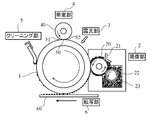
- FIG. 1 is a schematic diagram illustrating an example of an image forming apparatus using a charging roll according to an embodiment of the present disclosure.
- FIG. 2 is a cross-sectional view illustrating an example of a charging roll according to the embodiment of the present invention. It is sectional drawing of the rubber base material and surface layer cut
- the image forming apparatus includes a photoconductor 1.
- a developing unit 2 Around the photoconductor 1, a developing unit 2, an exposing unit 3, a charging unit 4, a transfer unit 6, and a cleaning unit 5 are arranged.
- the developing unit 2 is provided with a developing roll 20, a regulating blade 21, and a supply roll 22, and is filled with toner 23.
- the charging unit 4 is provided with a charging roll 40.
- the transfer unit 6 transfers the toner image to a paper sheet 60 as a recording medium.
- the toner image transferred by the transfer unit 6 is fixed by a fixing unit (not shown).
- the cylindrical and rotating photoreceptor 1 and the cylindrical and rotating charging roll 40 come into contact at the nip 50.
- the area between the photoconductor 1 and the charging roll 40 is changed. Discharge occurs, and the surface of the photoconductor 1 is charged.
- the charged state of the surface of the photoconductor 1 is preferably uniform over the circumferential direction and the axial direction of the photoconductor 1.
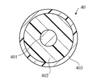
- FIG. 2 is a sectional view showing an example of the charging roll according to the embodiment of the present invention.
- the charging roll 40 has a core 401, a rubber base 402 formed on the outer peripheral surface of the core 401, and a surface layer 403 coated on the outer peripheral surface of the rubber base 402.
- a surface layer 403 on the outer peripheral surface of the rubber base material 402 with a coating component and making the surface state of the surface layer 403 appropriate, discharge unevenness between the photoreceptor 1 and the charging roll 40 is eliminated.
- the developing unit 2 can cause the developing unit 2 to adhere the amount of toner exactly corresponding to the latent image formed by the exposure unit 3 to the surface of the photoconductor 1.
- the core material 401 can be formed of, but not limited to, a metal or a resin material having excellent thermal conductivity and mechanical strength, such as stainless steel, nickel (Ni), a nickel alloy, and iron (Fe). ), Magnetic stainless steel, metal materials such as cobalt-nickel (Co-Ni) alloy, and resin materials such as PI (polyimide resin).
- the structure of the core material 401 is not particularly limited, and may be hollow or not hollow.
- the rubber base 402 is disposed on the outer peripheral surface of the core 401 and is made of conductive rubber having conductivity.
- the rubber base 402 may have one layer or two or more layers. Further, an adhesive layer, an adjustment layer, and the like may be provided between the core material 401 and the rubber substrate 402 as necessary.
- the rubber substrate 402 can be formed by molding a rubber composition obtained by adding a conductivity-imparting material, a crosslinking agent, and the like to a conductive rubber, around the core material 401.
- the conductive rubber include polyurethane rubber (PUR), epichlorohydrin rubber (ECO), nitrile rubber (NBR), styrene rubber (SBR), and chloroprene rubber (CR).
- an electronic conductivity imparting material such as carbon black and metal powder, an ionic conductivity imparting material, or a mixture thereof can be used.
- Examples of the ionic conductivity-imparting material include organic salts, inorganic salts, metal complexes, and ionic liquids.
- Examples of the organic salts include sodium trifluoride acetate, and examples of the inorganic salts include lithium perchlorate and quaternary ammonium salts.
- examples of the metal complex include ferric halide-ethylene glycol and the like, and specific examples thereof include those described in Japanese Patent No. 36555364.
- the ionic liquid is a molten salt that is liquid at room temperature and is also called a room temperature molten salt, and particularly has a melting point of 70 ° C. or less, preferably 30 ° C. or less. Specifically, those described in JP-A-2003-202722 can be exemplified.
- the crosslinking agent is not particularly limited, and includes, for example, sulfur and a peroxide vulcanizing agent.
- a crosslinking aid or the like which promotes the function of the crosslinking agent may be added to the rubber composition, if necessary.
- the crosslinking aid include inorganic zinc oxide and magnesium oxide, and organic stearic acid and amines.
- a thiazole-based or other crosslinking accelerator may be used.
- Other additives may be added to the rubber composition as needed.
- the surface of the rubber substrate 402 formed on the outer peripheral surface of the core material 401 is polished by a grinder, adjusted to a predetermined thickness, and then subjected to dry polishing with a polishing grindstone.
- a surface layer 403 is formed on the outer peripheral surface of the layer 402. The polishing is performed in this manner in order to appropriately adjust the surface roughness of the rubber base material 402 and to adjust the surface condition of the outer surface layer 403 outside the rubber base material 402.
- the surface roughness of the rubber substrate 402 (JIS B 0601: ten-point average roughness conforming to 1994 (ten point height of irregularities) ) R Z is 8. Preferably it is 5 ⁇ m or less. In this case, the surface roughness RZ is a value measured by a contact type surface roughness meter.
- Dry polishing is performed, for example, by moving a rotary grindstone in the axial direction while contacting the rubber base 402 with the rubber base 402 being rotated (traverse polishing).
- the number of revolutions of the grindstone of the polishing machine may be sequentially increased, for example, to 1000 rpm, 2000 rpm, and 3000 rpm during rotation.
- the type of the polishing grindstone may be changed.
- the polishing may be performed by sequentially increasing the number of a GC (green @ carborundum) grindstone like GC60, GC120, and GC220.
- the surface of the rubber substrate 402 may be further polished by wet polishing with a wet polisher using a waterproof abrasive paper or the like.
- polishing is performed by using a water-resistant polishing paper, for example, a water-resistant sandpaper, and abutting the rubber base 402 in a rotating state while supplying a polishing liquid thereto.
- the hardness of the rubber substrate 402 measured using a durometer (“Type A” based on “JIS K 6253” and “ISO 7619”) is preferably in the range of 50 ° to 64 °.
- the hardness of the surface of the charging roll 40 is affected by the rubber base 402. If the hardness of the rubber substrate 402 is less than 50 °, the convex portions on the surface of the charging roll 40 will be crushed, and the photoreceptor 1 will be easily stained, and image defects will occur. On the other hand, if the hardness of the rubber base 402 is greater than 64 °, the projections on the surface of the charging roll 40 may be reflected on the image.
- the surface layer 403 can be formed by applying a coating liquid to the outer peripheral surface of the rubber base material 402 and drying and curing the coating liquid.
- a coating liquid As a method of applying the coating liquid, a dip coating method, a roll coating method, a spray coating method, or the like can be used.
- the cured surface layer 403 has a conductive matrix 404 and particles 405 of, for example, an insulating surface roughness imparting material (also referred to as a roughness imparting material) dispersed in the conductive matrix 404. .
- the particles 405 of the roughness imparting material give the surface layer 403 an appropriate surface roughness.
- the conductive matrix 404 has a role of holding the particles 405 of the roughness-imparting material at a fixed position and a role of discharging the photoconductor 1.
- the conductive matrix 404 has a base material and a conductive agent dispersed in the base material. As described above, a discharge occurs between the charging roll 40 and the photoconductor 1 in the region 51 (and in some cases, the region 52).
- the particles 405 of the roughness imparting material are not completely buried in the conductive matrix 404, but may be completely buried.
- the conductive matrix 404 has an appropriate thickness for the diameter of the roughness-imparting material particles 405 because the ability to retain the roughness-imparting material particles 405 is low. It is preferred to have
- the roughness imparting material particles 405 are insulators, the thickness of the conductive matrix 404 is large, and the electric resistance of the conductive matrix 404 is large, discharge tends to be difficult to occur. By increasing the proportion of the conductive agent contained in the matrix 404, the electric resistance of the conductive matrix 404 can be reduced and discharge can be easily generated.
- the surface state of the surface layer 403 is adjusted by dispersing the particles 405 of the roughness-imparting material on the surface layer 403 formed on the rubber substrate 402 having the adjusted surface roughness. I have.
- the thickness of the conductive matrix 404 of the surface layer 403 is preferably within an appropriate numerical range. If the thickness is too large, it is considered that the surface roughness of the surface layer 403 becomes too small and causes image unevenness.
- the content of the particles 405 of the roughness-imparting material in the surface layer 403 is preferably in an appropriate numerical range.
- the particle content is high, the particles overlap each other, so that the surface of the surface layer 403 becomes rough, which is considered to cause image unevenness.
- the components of the coating liquid as the material of the surface layer 403 include at least particles 405 of the base material, the conductive agent, and the surface roughness imparting material. After the curing of the coating liquid, the base material and the conductive agent become components of the conductive matrix 404.
- the coating liquid is obtained, for example, by dissolving components of the following composition in a diluting solvent.
- -Base material 10 to 80 parts by weight.
- -Conductive agent 1 to 50 parts by weight.
- -Surface roughness imparting material 70% by weight or less of the total amount of the coating liquid.
- the discharge between the charging roll 40 and the photoconductor 1 is substantially uniform in the gap before the nip where the charging roll 40 and the photoconductor 1 come into contact, and uneven discharge occurs during image formation. It is considered that an image having a desired density is formed without causing the image formation, and the image quality is improved.
- the surface state of the surface layer 403 can be appropriately adjusted by appropriately adjusting the particle size and the amount of the particles 405 of the surface roughness imparting material.
- the base material contained in the coating liquid is an insulator.
- As the base material urethane resin, acrylic resin, acrylic urethane resin, amino resin, silicone resin, fluorine resin, polyamide resin, epoxy resin, polyester resin, polyether resin, phenol resin, urea resin, polyvinyl butyral resin, melamine resin, Nylon resin and the like can be mentioned. These base materials can be used alone or in any combination.
- conductive agent contained in the coating liquid examples include carbon black such as acetylene black, Ketjen black, and talka black, carbon nanotubes, ions such as lithium perchlorate, and ions such as 1-butyl-3-methylimidazolium hexafluorophosphate. Ionic liquids, metal oxides such as tin oxide, and conductive polymers. These conductive agents can be used alone or in any combination.
- ⁇ Surface roughness imparting material> As the particles 405 of the surface roughness imparting material contained in the coating liquid, acrylic particles, urethane particles, polyamide resin particles, silicone resin particles, fluororesin particles, styrene resin particles, phenol resin particles, polyester resin particles, olefin resin particles, Epoxy resin particles, nylon resin particles, carbon, graphite, balun, silica, alumina, titanium oxide, zinc oxide, magnesium oxide, zirconium oxide, calcium sulfate, calcium carbonate, magnesium carbonate, calcium silicate, aluminum nitride, boron nitride, Examples include talc, kaolin clay, diatomaceous earth, glass beads, hollow glass spheres, and the like. These particles can be used alone or in any combination.
- the diluting solvent contained in the coating liquid is not particularly limited, but may be aqueous, or methyl acetate, ethyl acetate, butyl acetate, methyl ethyl ketone (MEK), methyl isobutyl ketone (MIBK), methanol, ethanol, butanol, 2-propanol ( Solvent systems such as IPA), acetone, toluene, xylene, hexane, heptane, chloroform and the like.
- the kneaded rubber composition was made into a sheet-like material, wound around a surface of a core material 401 (core metal) having a diameter of 6 mm, pressed, and pressed to obtain a rubber substrate 402 made of crosslinked epichlorohydrin rubber.
- the measured value was 50 ° to 64 °. .
- the surface of the rubber substrate 402 was polished by a polishing machine. Specifically, the surface of the obtained rubber base material 402 is polished by a grinder to adjust to a predetermined thickness (1.25 mm), and then the grindstone rotation speed of the grinder is set to 1000 rpm, 2000 rpm, 3000 rpm, or the like. And polished by dry polishing. That is, in Experiment 1, the surface roughness of the rubber substrate 402 was reduced as much as possible.
- a coating liquid for forming the surface layer 403 on the outer peripheral surface of the rubber substrate 402 was prepared.
- composition of the coating liquid is as shown in Table 1.
- samples having different surface states of the surface layer 403 were manufactured by applying a coating solution containing particles 405 of different sizes and different amounts of the surface roughness imparting material.
- the particle size and amount of the particles 405 in these samples are as shown in Table 2.
- Samples 1 to 11 are the samples of Experiment 1.
- the surface layer 403 does not include the particles 405 of the roughness imparting material.
- the coating liquid having the above composition was dispersed and mixed in a ball mill for 3 hours.
- ⁇ Preparation of charging roll> The coating solution was applied to the polished outer peripheral surface of the rubber substrate 402 to form a surface layer 403, and the charging roll 40 was produced. Specifically, the coating solution is stirred, the solution is spray-coated on the surface of the rubber substrate 402, and dried at 120 ° C. for 60 minutes in an electric furnace to form the surface layer 403 on the outer peripheral surface of the rubber substrate 402. Then, a charging roll was prepared.
- the surface of the central portion of the charging roll 40 in the axial direction was photographed using a non-contact laser microscope.
- the laser microscope used was “VK-X200” manufactured by Keyence Corporation (Osaka, Japan).
- the magnification was 400 times, and the field of view was 528.7 ⁇ m in the circumferential direction of the charging roll 40 and 705.1 ⁇ m in the axial direction of the charging roll 40.
- quadratic surface correction of the geometric data obtained by the photographing was performed using Version 1.2.0.116 of the multi-file analysis application “VK-H1XM” manufactured by Keyence Corporation.
- the quadratic surface correction is a process of removing a data component corresponding to the cylindrical surface of the cylindrical surface of the charging roll 40 from the geometric data obtained by photographing. In other words, this is a process of converting the geometric data of the cylindrical surface obtained by imaging into the geometric data for the plane.
- the arithmetic mean tune S pc at the peak was calculated by this application.
- the value of Wolf pruning in the calculation of the arithmetic mean tune S pc at the peak was 5%. That is, the arithmetic mean tune S pc at the peak is calculated from a region having an amplitude larger than 5% of the maximum amplitude (the difference between the maximum height and the minimum height) of the contour curve.
- the arithmetic mean tune S pc at the peak obtained in this way is as shown in Table 2.
- the charging roll was applied to a copying machine, and the images printed under the following printing conditions (halftone image and solid white image) were evaluated for image unevenness. Table 2 shows the results.
- local discharge was determined for a halftone image, and brightness was determined for a solid white image.
- the occurrence of the local discharge can be confirmed by visually detecting the occurrence of white spots, black spots, white streaks, and black streaks in the halftone image.
- L * values L * value, lightness
- the reason for measuring the lightness is to determine the presence or absence of background stain, that is, fog (printed in a place that should not be printed).
- the kneaded rubber composition was made into a sheet-like material, wound around the surface of a core material 401 (core metal) having a diameter of 8 mm, press-molded, and a rubber substrate 402 made of crosslinked epichlorohydrin rubber was obtained.
- the measured value was 50 ° to 64 °. .
- the surface of the rubber substrate 402 was polished by a polishing machine. Specifically, the surface of the obtained rubber base material 402 was polished with a polishing machine to a predetermined thickness (2 mm), and then polished by dry polishing. In Experiment 2, the wheel rotation speed was not changed.
- a coating liquid for forming the surface layer 403 on the outer peripheral surface of the rubber substrate 402 was prepared.
- composition of the coating liquid is as shown in Table 1.
- the relationship between the average particle size of the urethane beads and the product name is as follows. However, in practice, one product contains particles having a particle size different from the average particle size. 6 ⁇ m: urethane beads “C-800” 10 ⁇ m: urethane beads “C-600” 15 ⁇ m: urethane beads “C-400” 22 ⁇ m: Urethane beads “C-300” 32 ⁇ m: urethane beads “C-200”
- samples having different surface states of the surface layer 403 were produced by applying a coating liquid containing particles 405 of different sizes and different amounts of the surface roughness imparting material.
- the particle size and amount of the particles 405 in these samples are as shown in Table 2.
- Samples 21 to 35 are the samples of Experiment 2.
- the coating liquid having the above composition was dispersed and mixed in a ball mill for 3 hours.
- ⁇ Preparation of charging roll> The coating solution was applied to the polished outer peripheral surface of the rubber substrate 402 to form a surface layer 403, and the charging roll 40 was produced. Specifically, the coating solution is stirred, the solution is spray-coated on the surface of the rubber substrate 402, and dried at 120 ° C. for 60 minutes in an electric furnace to form the surface layer 403 on the outer peripheral surface of the rubber substrate 402. Then, a charging roll was prepared.
- the DC voltage was a normal voltage (REF), and the AC voltage Vpp was dependent on the copier control.
- the charging roll was applied to a copying machine, and image unevenness was evaluated for images (halftone images and solid white images) printed under the following printing conditions. Table 3 shows the results.
- image unevenness local discharge was determined for a halftone image. The occurrence of the local discharge can be confirmed by visually detecting the occurrence of white spots, black spots, white streaks, and black streaks in the halftone image. With respect to the white solid image, the background stain, that is, fog was visually determined.
- the arithmetic mean tune S pc at the peak of the surface of the surface layer 403 is not less than 1,880 (1 / mm) and not more than 14,024 (1 / mm).
- the charging roll has been described as an embodiment, but the conductive roll according to the present invention is, in addition to a charging roll of an image forming apparatus such as an electrophotographic copying machine or a printer, a developing roll, a transfer roll, a charge removing roll,
- the present invention is also applicable to a toner supply roll and the like.
- photoconductor 2 developing unit 20: developing roll 21: regulating blade 22: supply roll 23: toner 3: exposure unit 4: charging unit 40: charging roll 401: core material 402: rubber substrate 403: surface layer 5: cleaning Unit 6: transfer unit 60: sheet
Abstract
This conductive roll is provided with a core material, a rubber base material that is arranged around the core material, and a surface layer that is arranged around the rubber base material. The surface of the surface layer has an arithmetic mean peak curvature Spc of from 1,880 (1/mm) to 14,024 (1/mm) (inclusive).
Description
本発明は、画像形成装置の帯電ロールなどに用いられる導電性ロールに関する。
The present invention relates to a conductive roll used for a charging roll of an image forming apparatus.
電子写真式複写機等の画像形成装置における画質は、感光体の帯電状態の均一性に依存しており、帯電ロールの表面粗さが、帯電状態の均一性に影響する。従来、帯電ロールの表面粗さに言及した技術としては、特許文献1~3が知られている。
画質 The image quality of an image forming apparatus such as an electrophotographic copying machine depends on the uniformity of the charged state of the photoconductor, and the surface roughness of the charging roll affects the uniformity of the charged state. Conventionally, Patent Literatures 1 to 3 are known as techniques that refer to the surface roughness of a charging roll.
特許文献1には、導電性支持体と、導電性支持体上に積層された導電性弾性体層と、導電性弾性体層上に最外層として積層された導電性樹脂層とからなる帯電部材(帯電ロール)に関する技術が記載されている。導電性樹脂層はマトリックス材料と、樹脂粒子及び無機粒子からなる群より選択される少なくとも一種の粒子を含有し、粒子は第一の粒子を含有し、導電性樹脂層におけるマトリックス材料単独で形成される部分の層厚をA[μm]、粒子の平均粒子径をB1[μm]、及び粒子の粒子間距離をSm[μm]としたとき、Aが10μm~7.0μmであり、B1/Aが5.0~30.0であり、Smが50μm~400μmである。
Patent Document 1 discloses a charging member including a conductive support, a conductive elastic layer laminated on the conductive support, and a conductive resin layer laminated as an outermost layer on the conductive elastic layer. (Charging roll) is described. The conductive resin layer contains a matrix material and at least one kind of particles selected from the group consisting of resin particles and inorganic particles, the particles contain the first particles, and the matrix material alone in the conductive resin layer is formed. that the layer thickness of the portions a [μm], an average particle diameter of the particles B1 [μm], and when the distance between particles of the particles was S m [μm], a is 10μm ~ 7.0μm, B1 / a is 5.0 ~ 30.0, S m is 50 [mu] m ~ 400 [mu] m.
特許文献2には、正帯電単層型電子写真感光体と、感光体の表面を帯電するための接触帯電部材を有する帯電装置と、帯電された像担持体の表面を露光して、像担持体の表面に静電潜像を形成するための露光装置と、静電潜像をトナー像として現像するための現像装置と、トナー像を像担持体から被転写体へ転写するための転写装置とを備える画像形成装置に関する技術が記載されている。接触帯電部材は、ゴム硬度がAsker-C硬度で62°~81°である導電性のゴムからなる帯電ローラであり、接触帯電部材の帯電ローラのローラ表面粗度が、凹凸の平均間隔Smで55μm~130μmであり、かつ十点平均粗さRZで9μm~19μmである。
Patent Document 2 discloses a positively charged single-layer type electrophotographic photoreceptor, a charging device having a contact charging member for charging the surface of the photoreceptor, and a method for exposing the surface of a charged image carrier to an image carrier. An exposure device for forming an electrostatic latent image on the surface of a body, a developing device for developing the electrostatic latent image as a toner image, and a transfer device for transferring a toner image from an image carrier to a transfer target There is described a technology relating to an image forming apparatus having the following. The contact charging member is a charging roller made of a conductive rubber having a rubber hardness of 62 ° to 81 ° in Asker-C hardness. The roller surface roughness of the charging roller of the contact charging member has an average spacing S m of unevenness. in a 55 .mu.m ~ 130 .mu.m, and a ten-point mean roughness R Z is 9 .mu.m ~ 19 .mu.m.
特許文献3には、導電性支持体と、導電性支持体上にロール状に形成された半導電性弾性層と、半導電性弾性層の表面に形成された保護層とを具備する帯電ローラに関する技術が記載されている。保護層は、保護層への外部物質の付着を防止する機能を発現する微粒子を含有した保護層形成用塗工液を塗工することにより形成され、微粒子の体積平均粒径は保護層の表面粗さが1μm以下となるように微細化されている。
Patent Document 3 discloses a charging roller including a conductive support, a semiconductive elastic layer formed in a roll shape on the conductive support, and a protective layer formed on the surface of the semiconductive elastic layer. Technology is described. The protective layer is formed by applying a protective layer-forming coating solution containing fine particles exhibiting a function of preventing external substances from adhering to the protective layer, and the volume average particle diameter of the fine particles is determined by the surface of the protective layer. It is miniaturized so that the roughness is 1 μm or less.
特許文献1~3によれば、帯電ロールの最表面の表面粗さを、表層に含有させた微粒子により調整することで、帯電ロールと感光体間の放電をできるだけ均一化して、画像品質を向上させようとする。
According to Patent Documents 1 to 3, the surface roughness of the outermost surface of the charging roll is adjusted by the fine particles contained in the surface layer, thereby making the discharge between the charging roll and the photoreceptor as uniform as possible and improving the image quality. Try to let it.
画像形成装置に対して、高い画像品質の要求が高まっている。
高 い There is an increasing demand for high image quality for image forming apparatuses.
本発明は、画像ムラを低減することが可能な導電性ロールを提供することを目的とする。
は An object of the present invention is to provide a conductive roll capable of reducing image unevenness.
本発明に係る導電性ロールは、芯材と、前記芯材の周囲に配置されたゴム基材と、前記ゴム基材の周囲に配置された表層とを備え、前記表層の表面の山頂点の算術平均曲(arithmetic mean peak curvature)Spcが、1,880(1/mm)以上、14,024(1/mm)以下である。この態様によれば、画像ムラを低減することができる。
The conductive roll according to the present invention includes a core material, a rubber base material arranged around the core material, and a surface layer arranged around the rubber base material. The arithmetic mean peak curvature S pc is not less than 1,880 (1 / mm) and not more than 14,024 (1 / mm). According to this aspect, image unevenness can be reduced.
好ましくは、前記表層は、絶縁体から形成されたベース材と前記ベース材に分散された導電材を含む導電性マトリックスと、前記導電性マトリックスに分散された表面粗さ付与材の粒子を有する。
Preferably, the surface layer has a base material formed of an insulator, a conductive matrix including a conductive material dispersed in the base material, and particles of a surface roughness imparting material dispersed in the conductive matrix.
好ましくは、前記表面粗さ付与材の粒子は、絶縁体から形成されている。
Preferably, the particles of the surface roughness imparting material are formed of an insulator.
以下に、本発明を実施するための形態を詳細に説明する。以下、導電性ロールの例として、帯電ロールを説明する。図面において縮尺は、必ずしも実施形態の製品またはサンプルを正確に表してはおらず、一部の寸法を誇張して表現している場合もある。
Hereinafter, embodiments for carrying out the present invention will be described in detail. Hereinafter, a charging roll will be described as an example of the conductive roll. In the drawings, the scale does not necessarily accurately represent the product or the sample of the embodiment, and some dimensions may be exaggerated in some cases.
図1に示すように、本発明の実施形態に係る画像形成装置は、感光体1を備える。感光体1の周囲には、現像部2、露光部3、帯電部4、転写部6及びクリーニング部5が配置されている。現像部2には、現像ロール20、規制ブレード21及び供給ロール22が設けられ、トナー23が充填されている。帯電部4には、帯電ロール40が設けられている。転写部6は、記録媒体である紙のシート60にトナー画像を転写する。転写部6で転写されたトナー画像は、図示しない定着部で定着される。
As shown in FIG. 1, the image forming apparatus according to the embodiment of the present invention includes a photoconductor 1. Around the photoconductor 1, a developing unit 2, an exposing unit 3, a charging unit 4, a transfer unit 6, and a cleaning unit 5 are arranged. The developing unit 2 is provided with a developing roll 20, a regulating blade 21, and a supply roll 22, and is filled with toner 23. The charging unit 4 is provided with a charging roll 40. The transfer unit 6 transfers the toner image to a paper sheet 60 as a recording medium. The toner image transferred by the transfer unit 6 is fixed by a fixing unit (not shown).
円柱状であり回転する感光体1と円柱状であり回転する帯電ロール40は、ニップ50で接触する。感光体1と帯電ロール40の回転方向におけるニップ50の手前の領域51(場合によっては、手前の領域51に加えてニップ50の後の領域52)において、感光体1と帯電ロール40の間で放電が起こり、感光体1の表面が帯電される。感光体1の表面の帯電状態は、感光体1の周方向および軸線方向にわたって一様であることが好ましい。
感光 The cylindrical and rotating photoreceptor 1 and the cylindrical and rotating charging roll 40 come into contact at the nip 50. In the region 51 before the nip 50 in the rotation direction of the photoconductor 1 and the charging roll 40 (in some cases, the region 52 after the nip 50 in addition to the front region 51), the area between the photoconductor 1 and the charging roll 40 is changed. Discharge occurs, and the surface of the photoconductor 1 is charged. The charged state of the surface of the photoconductor 1 is preferably uniform over the circumferential direction and the axial direction of the photoconductor 1.
図2は、本発明の実施形態に係る帯電ロールの一例を示す断面図である。図2に示すように、帯電ロール40は、芯材401と、芯材401の外周面に形成されたゴム基材402と、ゴム基材402の外周面にコーティングされた表層403とを有する。ゴム基材402の外周面にコーティング成分によって表層403を形成し、その表層403の表面状態を適切にすることにより、感光体1と帯電ロール40の間の放電ムラが解消されて、感光体1に均一に放電することが可能となり、露光部3で形成された潜像に正確に対応する量のトナーを現像部2は感光体1の表面に付着させることができる。
FIG. 2 is a sectional view showing an example of the charging roll according to the embodiment of the present invention. As shown in FIG. 2, the charging roll 40 has a core 401, a rubber base 402 formed on the outer peripheral surface of the core 401, and a surface layer 403 coated on the outer peripheral surface of the rubber base 402. By forming a surface layer 403 on the outer peripheral surface of the rubber base material 402 with a coating component and making the surface state of the surface layer 403 appropriate, discharge unevenness between the photoreceptor 1 and the charging roll 40 is eliminated. Thus, the developing unit 2 can cause the developing unit 2 to adhere the amount of toner exactly corresponding to the latent image formed by the exposure unit 3 to the surface of the photoconductor 1.
<芯材>
芯材401は、限定されるわけではないが、熱伝導性及び機械的強度に優れた金属又は樹脂材料から形成することができ、例えば、ステンレス鋼、ニッケル(Ni)、ニッケル合金、鉄(Fe)、磁性ステンレス、コバルト-ニッケル(Co-Ni)合金等の金属材料や、PI(ポリイミド樹脂)等の樹脂材料から形成することができる。また、芯材401の構造についても特に制限はなく、中空であっても、中空でなくてもよい。 <Core material>
Thecore material 401 can be formed of, but not limited to, a metal or a resin material having excellent thermal conductivity and mechanical strength, such as stainless steel, nickel (Ni), a nickel alloy, and iron (Fe). ), Magnetic stainless steel, metal materials such as cobalt-nickel (Co-Ni) alloy, and resin materials such as PI (polyimide resin). The structure of the core material 401 is not particularly limited, and may be hollow or not hollow.
芯材401は、限定されるわけではないが、熱伝導性及び機械的強度に優れた金属又は樹脂材料から形成することができ、例えば、ステンレス鋼、ニッケル(Ni)、ニッケル合金、鉄(Fe)、磁性ステンレス、コバルト-ニッケル(Co-Ni)合金等の金属材料や、PI(ポリイミド樹脂)等の樹脂材料から形成することができる。また、芯材401の構造についても特に制限はなく、中空であっても、中空でなくてもよい。 <Core material>
The
<ゴム基材>
ゴム基材402は、芯材401の外周面に配置されており、導電性を有する導電性ゴムによって形成されている。ゴム基材402は、1層であっても、2層以上であってもよい。また、芯材401とゴム基材402の間に、必要に応じて密着層や調整層等を設けてもよい。 <Rubber substrate>
Therubber base 402 is disposed on the outer peripheral surface of the core 401 and is made of conductive rubber having conductivity. The rubber base 402 may have one layer or two or more layers. Further, an adhesive layer, an adjustment layer, and the like may be provided between the core material 401 and the rubber substrate 402 as necessary.
ゴム基材402は、芯材401の外周面に配置されており、導電性を有する導電性ゴムによって形成されている。ゴム基材402は、1層であっても、2層以上であってもよい。また、芯材401とゴム基材402の間に、必要に応じて密着層や調整層等を設けてもよい。 <Rubber substrate>
The
ゴム基材402は、導電性ゴムに導電性付与材や架橋剤等を添加して得られたゴム組成物を、芯材401の周囲に、成形することによって形成できる。導電性ゴムとしては、ポリウレタンゴム(PUR)、エピクロルヒドリンゴム(ECO)、ニトリルゴム(NBR)、スチレンゴム(SBR)、クロロプレンゴム(CR)等を挙げることができる。
(4) The rubber substrate 402 can be formed by molding a rubber composition obtained by adding a conductivity-imparting material, a crosslinking agent, and the like to a conductive rubber, around the core material 401. Examples of the conductive rubber include polyurethane rubber (PUR), epichlorohydrin rubber (ECO), nitrile rubber (NBR), styrene rubber (SBR), and chloroprene rubber (CR).
導電性付与材としては、カーボンブラック、金属粉等の電子導電性付与材、イオン導電付与材、又はこれらを混合して用いることができる。
電子 As the conductivity imparting material, an electronic conductivity imparting material such as carbon black and metal powder, an ionic conductivity imparting material, or a mixture thereof can be used.
イオン導電付与材としては、有機塩類、無機塩類、金属錯体、イオン性液体等が挙げられる。有機塩類としては、三フッ化酢酸ナトリウム等が挙げられ、無機塩類としては、過塩素酸リチウム、4級アンモニウム塩等が挙げられる。また、金属錯体としては、ハロゲン化第二鉄-エチレングリコール等が挙げられ、具体的には、特許第3655364号公報に記載されたものを挙げることができる。イオン性液体は、室温で液体である溶融塩であり、常温溶融塩とも呼ばれるものであり、特に、融点が70℃以下、好ましくは30℃以下のものをいう。具体的には、特開2003-202722号公報に記載されたものを挙げることができる。
Examples of the ionic conductivity-imparting material include organic salts, inorganic salts, metal complexes, and ionic liquids. Examples of the organic salts include sodium trifluoride acetate, and examples of the inorganic salts include lithium perchlorate and quaternary ammonium salts. Further, examples of the metal complex include ferric halide-ethylene glycol and the like, and specific examples thereof include those described in Japanese Patent No. 36555364. The ionic liquid is a molten salt that is liquid at room temperature and is also called a room temperature molten salt, and particularly has a melting point of 70 ° C. or less, preferably 30 ° C. or less. Specifically, those described in JP-A-2003-202722 can be exemplified.
また、架橋剤としては、特に限定されず、例えば、硫黄や過酸化物加硫剤等が挙げられる。
The crosslinking agent is not particularly limited, and includes, for example, sulfur and a peroxide vulcanizing agent.
さらに、ゴム組成物には、必要に応じて架橋剤の働きを促進させる架橋助剤等を加えてもよい。架橋助剤としては、無機系の酸化亜鉛や酸化マグネシウム、有機系のステアリン酸やアミン類等が挙げられる。また、架橋時間の短縮等の目的で、チアゾール系、またはその他の架橋促進剤を用いてもよい。ゴム組成物には、必要に応じて他の添加剤を加えてもよい。
架橋 Furthermore, a crosslinking aid or the like which promotes the function of the crosslinking agent may be added to the rubber composition, if necessary. Examples of the crosslinking aid include inorganic zinc oxide and magnesium oxide, and organic stearic acid and amines. For the purpose of shortening the crosslinking time, a thiazole-based or other crosslinking accelerator may be used. Other additives may be added to the rubber composition as needed.
本実施形態において、芯材401の外周面に形成されたゴム基材402の表面を研磨機で研磨し、所定の厚さに合わせた後、研磨砥石による乾式研磨を行った後に、ゴム基材402の外周面に表層403を形成する。このように研磨を行うのは、ゴム基材402の表面粗さを適切に調整し、その外側の表層403の表面状態を調整するためである。
In the present embodiment, the surface of the rubber substrate 402 formed on the outer peripheral surface of the core material 401 is polished by a grinder, adjusted to a predetermined thickness, and then subjected to dry polishing with a polishing grindstone. A surface layer 403 is formed on the outer peripheral surface of the layer 402. The polishing is performed in this manner in order to appropriately adjust the surface roughness of the rubber base material 402 and to adjust the surface condition of the outer surface layer 403 outside the rubber base material 402.
ゴム基材402の表面粗さを極力小さくする場合、ゴム基材402の表面粗さ(JIS B 0601:1994に準拠する十点平均粗さ(ten point height of irregularities))RZは、8.5μm以下であることが好ましい。この場合、表面粗さRZは、接触式の表面粗さ計により測定された値である。
When to minimize the surface roughness of the rubber base material 402, the surface roughness of the rubber substrate 402 (JIS B 0601: ten-point average roughness conforming to 1994 (ten point height of irregularities) ) R Z is 8. Preferably it is 5 μm or less. In this case, the surface roughness RZ is a value measured by a contact type surface roughness meter.
乾式研磨は、例えば、ゴム基材402を回転させた状態で、回転砥石をゴム基材402に接触させながら軸方向に移動させることにより行う(トラバース研磨)。ゴム基材402の表面粗さを極力小さくする場合には、回転の際に、例えば、研磨機の砥石回転数を1000rpm、2000rpm、3000rpmのように順次上げてもよい。或いは、研磨砥石の種類を変更してもよく、例えば、GC(green carborundum)砥石番手をGC60、GC120、GC220のように順次上げて研磨してもよい。
Dry polishing is performed, for example, by moving a rotary grindstone in the axial direction while contacting the rubber base 402 with the rubber base 402 being rotated (traverse polishing). When the surface roughness of the rubber substrate 402 is to be minimized, the number of revolutions of the grindstone of the polishing machine may be sequentially increased, for example, to 1000 rpm, 2000 rpm, and 3000 rpm during rotation. Alternatively, the type of the polishing grindstone may be changed. For example, the polishing may be performed by sequentially increasing the number of a GC (green @ carborundum) grindstone like GC60, GC120, and GC220.
また、ゴム基材402の表面を乾式研磨した後に、更に耐水研磨ペーパー等を用いて湿式研磨機で湿式研磨を施して研磨してもよい。ここで、湿式研磨は、耐水研磨ペーパー、例えば、耐水性のサンドペーパーを用い、これに研磨液を供給しながらゴム基材402を回転させた状態で当接させることにより研磨する。
Alternatively, after the surface of the rubber substrate 402 is dry polished, the surface may be further polished by wet polishing with a wet polisher using a waterproof abrasive paper or the like. Here, in the wet polishing, polishing is performed by using a water-resistant polishing paper, for example, a water-resistant sandpaper, and abutting the rubber base 402 in a rotating state while supplying a polishing liquid thereto.
<ゴム基材のゴム硬度>
ゴム基材402について、デュロメータ(「JIS K 6253」および「ISO 7619」に準拠した「タイプA」)を用いて測定した硬度は、50°~64°の範囲が好ましい。 <Rubber hardness of rubber substrate>
The hardness of therubber substrate 402 measured using a durometer (“Type A” based on “JIS K 6253” and “ISO 7619”) is preferably in the range of 50 ° to 64 °.
ゴム基材402について、デュロメータ(「JIS K 6253」および「ISO 7619」に準拠した「タイプA」)を用いて測定した硬度は、50°~64°の範囲が好ましい。 <Rubber hardness of rubber substrate>
The hardness of the
ゴム基材402の外側の表層403は薄いため、帯電ロール40の表面の硬度は、ゴム基材402に影響される。ゴム基材402の硬度が50°未満であると、帯電ロール40の表面の凸部が潰れて、感光体1が汚れやすく、画像不良が発生する。一方、ゴム基材402の硬度が64°より大きいと、帯電ロール40の表面の凸部が画像に反映されるおそれがある。
た め Since the outer layer 403 outside the rubber base 402 is thin, the hardness of the surface of the charging roll 40 is affected by the rubber base 402. If the hardness of the rubber substrate 402 is less than 50 °, the convex portions on the surface of the charging roll 40 will be crushed, and the photoreceptor 1 will be easily stained, and image defects will occur. On the other hand, if the hardness of the rubber base 402 is greater than 64 °, the projections on the surface of the charging roll 40 may be reflected on the image.
<表層>
本実施形態では、ゴム基材402の外周面に、コーティング液を塗布し、乾燥硬化させることにより、表層403を形成することができる。コーティング液を塗布する方法としては、ディップコート法、ロールコート法、スプレーコート法等を用いることができる。 <Surface>
In the present embodiment, thesurface layer 403 can be formed by applying a coating liquid to the outer peripheral surface of the rubber base material 402 and drying and curing the coating liquid. As a method of applying the coating liquid, a dip coating method, a roll coating method, a spray coating method, or the like can be used.
本実施形態では、ゴム基材402の外周面に、コーティング液を塗布し、乾燥硬化させることにより、表層403を形成することができる。コーティング液を塗布する方法としては、ディップコート法、ロールコート法、スプレーコート法等を用いることができる。 <Surface>
In the present embodiment, the
図3に示すように、硬化した表層403は、導電性マトリックス404と、導電性マトリックス404に分散された例えば絶縁性の表面粗さ付与材(粗さ付与材ともいう。)の粒子405を有する。粗さ付与材の粒子405は、表層403に適切な表面粗さを与える。導電性マトリックス404は、粗さ付与材の粒子405を固定位置に保持する役割と、感光体1に対する放電を行う役割を果たす。導電性マトリックス404は、ベース材とベース材に分散された導電剤を有する。上記の通り、領域51(および場合により領域52)において、帯電ロール40と感光体1の間で放電が起こる。
As shown in FIG. 3, the cured surface layer 403 has a conductive matrix 404 and particles 405 of, for example, an insulating surface roughness imparting material (also referred to as a roughness imparting material) dispersed in the conductive matrix 404. . The particles 405 of the roughness imparting material give the surface layer 403 an appropriate surface roughness. The conductive matrix 404 has a role of holding the particles 405 of the roughness-imparting material at a fixed position and a role of discharging the photoconductor 1. The conductive matrix 404 has a base material and a conductive agent dispersed in the base material. As described above, a discharge occurs between the charging roll 40 and the photoconductor 1 in the region 51 (and in some cases, the region 52).
図3に示す例では、粗さ付与材の粒子405は導電性マトリックス404内に完全に埋没していないが、完全に埋没していてもよい。導電性マトリックス404の厚さが小さい場合には、粗さ付与材の粒子405を保持する能力が低いため、粗さ付与材の粒子405の直径に対して、導電性マトリックス404は適切な厚さを有するのが好ましい。粗さ付与材の粒子405が絶縁体であって、導電性マトリックス404の厚さが大きく、導電性マトリックス404の電気抵抗が大きい場合には、放電が発生しにくくなりがちであるが、導電性マトリックス404に含まれる導電剤の割合を向上させることにより、導電性マトリックス404の電気抵抗を低減して、放電を発生させやすくすることができる。
で は In the example shown in FIG. 3, the particles 405 of the roughness imparting material are not completely buried in the conductive matrix 404, but may be completely buried. When the thickness of the conductive matrix 404 is small, the conductive matrix 404 has an appropriate thickness for the diameter of the roughness-imparting material particles 405 because the ability to retain the roughness-imparting material particles 405 is low. It is preferred to have When the roughness imparting material particles 405 are insulators, the thickness of the conductive matrix 404 is large, and the electric resistance of the conductive matrix 404 is large, discharge tends to be difficult to occur. By increasing the proportion of the conductive agent contained in the matrix 404, the electric resistance of the conductive matrix 404 can be reduced and discharge can be easily generated.
本実施形態においては、表面粗さが調整されたゴム基材402の上に形成された表層403に粗さ付与材の粒子405が分散されていることにより、表層403の表面状態が調整されている。
In the present embodiment, the surface state of the surface layer 403 is adjusted by dispersing the particles 405 of the roughness-imparting material on the surface layer 403 formed on the rubber substrate 402 having the adjusted surface roughness. I have.
本実施形態において、表層403の導電性マトリックス404の膜厚は、適切な数値範囲内にあることが好ましいと考えられる。この厚さが大きすぎる場合には、表層403の表面粗さが小さくなりすぎて、画像ムラの原因となると考えられる。
に お い て In the present embodiment, it is considered that the thickness of the conductive matrix 404 of the surface layer 403 is preferably within an appropriate numerical range. If the thickness is too large, it is considered that the surface roughness of the surface layer 403 becomes too small and causes image unevenness.
また、本実施形態において、表層403の粗さ付与材の粒子405の含有率は、適切な数値範囲内にあることが好ましいと考えられる。粒子含有量が多い場合、粒子同士が重なり合うため、表層403の表面が粗くなり、画像ムラの原因となると考えられる。
In addition, in the present embodiment, it is considered that the content of the particles 405 of the roughness-imparting material in the surface layer 403 is preferably in an appropriate numerical range. When the particle content is high, the particles overlap each other, so that the surface of the surface layer 403 becomes rough, which is considered to cause image unevenness.
本実施形態において、表層403の材料であるコーティング液の成分は、ベース材、導電剤及び表面粗さ付与材の粒子405を少なくとも含有する。コーティング液の硬化後に、ベース材と導電剤は、導電性マトリックス404の成分となる。
In the present embodiment, the components of the coating liquid as the material of the surface layer 403 include at least particles 405 of the base material, the conductive agent, and the surface roughness imparting material. After the curing of the coating liquid, the base material and the conductive agent become components of the conductive matrix 404.
コーティング液は、たとえば、下記組成の成分を希釈溶剤に溶解させて得られる。
・ベース材 :10重量部~80重量部。
・導電剤:1重量部~50重量部。
・表面粗さ付与材:コーティング液全量の70重量%以下。 The coating liquid is obtained, for example, by dissolving components of the following composition in a diluting solvent.
-Base material: 10 to 80 parts by weight.
-Conductive agent: 1 to 50 parts by weight.
-Surface roughness imparting material: 70% by weight or less of the total amount of the coating liquid.
表層403の表面状態が適切である場合に、帯電ロール40と感光体1が接触するニップの手前のギャップにおいて、帯電ロール40と感光体1間の放電がほぼ均一化され、画像形成時に放電ムラが生じることなく、所望の濃度の画像が形成され、画像品質が向上すると考えられる。
When the surface state of the surface layer 403 is appropriate, the discharge between the charging roll 40 and the photoconductor 1 is substantially uniform in the gap before the nip where the charging roll 40 and the photoconductor 1 come into contact, and uneven discharge occurs during image formation. It is considered that an image having a desired density is formed without causing the image formation, and the image quality is improved.
表面粗さ付与材の粒子405の粒径および添加量を適切に調整することにより、表層403の表面状態を適切に調整することができると考えられる。
It is considered that the surface state of the surface layer 403 can be appropriately adjusted by appropriately adjusting the particle size and the amount of the particles 405 of the surface roughness imparting material.
<ベース材>
コーティング液に含まれるベース材は絶縁体である。ベース材としては、ウレタン樹脂、アクリル樹脂、アクリルウレタン樹脂、アミノ樹脂、シリコーン樹脂、フッ素樹脂、ポリアミド樹脂、エポキシ樹脂、ポリエステル樹脂、ポリエーテル樹脂、フェノール樹脂、尿素樹脂、ポリビニルブチラール樹脂、メラミン樹脂、ナイロン樹脂等が挙げられる。これらのベース材は、単独で又は任意の組み合わせで用いることができる。 <Base material>
The base material contained in the coating liquid is an insulator. As the base material, urethane resin, acrylic resin, acrylic urethane resin, amino resin, silicone resin, fluorine resin, polyamide resin, epoxy resin, polyester resin, polyether resin, phenol resin, urea resin, polyvinyl butyral resin, melamine resin, Nylon resin and the like can be mentioned. These base materials can be used alone or in any combination.
<導電剤>
コーティング液に含まれる導電剤としては、アセチレンブラック、ケッチェンブラック、トーカブラック等のカーボンブラック、カーボンナノチューブ、過塩素リチウム等のイオン、ヘキサフルオロリン酸1-ブチル-3-メチルイミダゾリウム等のイオン性液体、酸化スズ等の金属酸化物、導電性ポリマーが挙げられる。これらの導電剤は、単独で又は任意の組み合わせで用いることができる。 <Conductive agent>
Examples of the conductive agent contained in the coating liquid include carbon black such as acetylene black, Ketjen black, and talka black, carbon nanotubes, ions such as lithium perchlorate, and ions such as 1-butyl-3-methylimidazolium hexafluorophosphate. Ionic liquids, metal oxides such as tin oxide, and conductive polymers. These conductive agents can be used alone or in any combination.
<表面粗さ付与材>
コーティング液に含まれる表面粗さ付与材の粒子405としては、アクリル粒子、ウレタン粒子、ポリアミド樹脂粒子、シリコーン樹脂粒子、フッ素樹脂粒子、スチレン樹脂粒子、フェノール樹脂粒子、ポリエステル樹脂粒子、オレフィン樹脂粒子、エポキシ樹脂粒子、ナイロン樹脂粒子、カーボン、グラファイト、炭化バルン、シリカ、アルミナ、酸化チタン、酸化亜鉛、酸化マグネシウム、酸化ジルコニウム、硫酸カルシウム、炭酸カルシウム、炭酸マグネシウム、ケイ酸カルシウム、窒化アルミニウム、窒化ホウ素、タルク、カオリンクレー、珪藻土、ガラスビーズ、中空ガラス球等が挙げられる。これらの粒子は、単独で又は任意の組み合わせで用いることができる。 <Surface roughness imparting material>
As theparticles 405 of the surface roughness imparting material contained in the coating liquid, acrylic particles, urethane particles, polyamide resin particles, silicone resin particles, fluororesin particles, styrene resin particles, phenol resin particles, polyester resin particles, olefin resin particles, Epoxy resin particles, nylon resin particles, carbon, graphite, balun, silica, alumina, titanium oxide, zinc oxide, magnesium oxide, zirconium oxide, calcium sulfate, calcium carbonate, magnesium carbonate, calcium silicate, aluminum nitride, boron nitride, Examples include talc, kaolin clay, diatomaceous earth, glass beads, hollow glass spheres, and the like. These particles can be used alone or in any combination.
コーティング液に含まれる表面粗さ付与材の粒子405としては、アクリル粒子、ウレタン粒子、ポリアミド樹脂粒子、シリコーン樹脂粒子、フッ素樹脂粒子、スチレン樹脂粒子、フェノール樹脂粒子、ポリエステル樹脂粒子、オレフィン樹脂粒子、エポキシ樹脂粒子、ナイロン樹脂粒子、カーボン、グラファイト、炭化バルン、シリカ、アルミナ、酸化チタン、酸化亜鉛、酸化マグネシウム、酸化ジルコニウム、硫酸カルシウム、炭酸カルシウム、炭酸マグネシウム、ケイ酸カルシウム、窒化アルミニウム、窒化ホウ素、タルク、カオリンクレー、珪藻土、ガラスビーズ、中空ガラス球等が挙げられる。これらの粒子は、単独で又は任意の組み合わせで用いることができる。 <Surface roughness imparting material>
As the
画像品質を向上するために、コーティング液中の表面粗さ付与材の粒子405の粒径と粒子含有率との関係については、好ましい範囲があると考えられる。
In order to improve the image quality, it is considered that there is a preferable range of the relationship between the particle size and the particle content of the particles 405 of the surface roughness imparting material in the coating liquid.
<希釈溶剤>
コーティング液に含まれる希釈溶剤としては、特に限定されないが、水系、又は、酢酸メチル、酢酸エチル、酢酸ブチル、メチルエチルケトン(MEK)、メチルイソブチルケトン(MIBK)、メタノール、エタノール、ブタノール、2-プロパノール(IPA)、アセトン、トルエン、キシレン、ヘキサン、ヘプタン、クロロホルム等の溶剤系等が挙げられる。 <Diluent solvent>
The diluting solvent contained in the coating liquid is not particularly limited, but may be aqueous, or methyl acetate, ethyl acetate, butyl acetate, methyl ethyl ketone (MEK), methyl isobutyl ketone (MIBK), methanol, ethanol, butanol, 2-propanol ( Solvent systems such as IPA), acetone, toluene, xylene, hexane, heptane, chloroform and the like.
以下、本実施形態の実施例を更に具体的に説明する。
Hereinafter, Examples of the present embodiment will be described more specifically.
実験1
<ゴム基材の準備>
エピクロルヒドリンゴム(エピクロマーCG-102;株式会社大阪ソーダ(日本国大阪府)製)100重量部に、導電性付与材としてトリフルオロ酢酸ナトリウム0.5重量部、亜鉛華3重量部、ステアリン酸2重量部、架橋剤1.5重量部を添加したゴム組成物をロールミキサーで混練りした。Experiment 1
<Preparation of rubber substrate>
100 parts by weight of epichlorohydrin rubber (Epichromer CG-102; manufactured by Osaka Soda Co., Ltd., Osaka, Japan), 0.5 parts by weight of sodium trifluoroacetate, 3 parts by weight of zinc white, 2 parts by weight of stearic acid as a conductivity-imparting material Parts, and 1.5 parts by weight of a crosslinking agent, were kneaded with a roll mixer.
<ゴム基材の準備>
エピクロルヒドリンゴム(エピクロマーCG-102;株式会社大阪ソーダ(日本国大阪府)製)100重量部に、導電性付与材としてトリフルオロ酢酸ナトリウム0.5重量部、亜鉛華3重量部、ステアリン酸2重量部、架橋剤1.5重量部を添加したゴム組成物をロールミキサーで混練りした。
<Preparation of rubber substrate>
100 parts by weight of epichlorohydrin rubber (Epichromer CG-102; manufactured by Osaka Soda Co., Ltd., Osaka, Japan), 0.5 parts by weight of sodium trifluoroacetate, 3 parts by weight of zinc white, 2 parts by weight of stearic acid as a conductivity-imparting material Parts, and 1.5 parts by weight of a crosslinking agent, were kneaded with a roll mixer.
混練りしたゴム組成物をシート状の生地にして、直径6mmの芯材401(芯金)の表面に巻いて、プレス成形し、架橋したエピクロルヒドリンゴムからなるゴム基材402を得た。
(4) The kneaded rubber composition was made into a sheet-like material, wound around a surface of a core material 401 (core metal) having a diameter of 6 mm, pressed, and pressed to obtain a rubber substrate 402 made of crosslinked epichlorohydrin rubber.
デュロメータ(「JIS K 6253」および「ISO 7619」に準拠した「タイプA」)を用いて、得られたゴム基材402の硬度を測定した結果、測定値は、50°~64°であった。
As a result of measuring the hardness of the obtained rubber base material 402 using a durometer (“Type A” based on “JIS K6253” and “ISO 7619”), the measured value was 50 ° to 64 °. .
<ゴム基材表面の研磨>
ゴム基材402の表面を研磨機で研磨した。具体的には、得られたゴム基材402の表面を研磨機で研磨して、所定の厚さ(1.25mm)に合わせた後、研磨機の砥石回転数を1000rpm、2000rpm、3000rpmのように順次上げて乾式研磨で研磨した。すなわち、実験1では、ゴム基材402の表面粗さを極力小さくした。 <Polishing of rubber substrate surface>
The surface of therubber substrate 402 was polished by a polishing machine. Specifically, the surface of the obtained rubber base material 402 is polished by a grinder to adjust to a predetermined thickness (1.25 mm), and then the grindstone rotation speed of the grinder is set to 1000 rpm, 2000 rpm, 3000 rpm, or the like. And polished by dry polishing. That is, in Experiment 1, the surface roughness of the rubber substrate 402 was reduced as much as possible.
ゴム基材402の表面を研磨機で研磨した。具体的には、得られたゴム基材402の表面を研磨機で研磨して、所定の厚さ(1.25mm)に合わせた後、研磨機の砥石回転数を1000rpm、2000rpm、3000rpmのように順次上げて乾式研磨で研磨した。すなわち、実験1では、ゴム基材402の表面粗さを極力小さくした。 <Polishing of rubber substrate surface>
The surface of the
<コーティング液の調製>
上記のゴム基材402の外周面に表層403を形成するためのコーティング液を作製した。 <Preparation of coating liquid>
A coating liquid for forming thesurface layer 403 on the outer peripheral surface of the rubber substrate 402 was prepared.
上記のゴム基材402の外周面に表層403を形成するためのコーティング液を作製した。 <Preparation of coating liquid>
A coating liquid for forming the
コーティング液の組成は、表1に示す通りである。

The composition of the coating liquid is as shown in Table 1.
ウレタン粒子としては、根上工業株式会社(日本国東京都)製のウレタンビーズを用いた。
(4) Urethane beads manufactured by Negami Industry Co., Ltd. (Tokyo, Japan) were used as the urethane particles.
ウレタンビーズの平均粒径と製品名との関係は以下の通りである。但し、実際には、一つの製品は、平均粒径と異なる粒径の粒子を含む。
6μm:ウレタンビーズ「C-800」
10μm:ウレタンビーズ「C-600」
15μm:ウレタンビーズ「C-400」
22μm:ウレタンビーズ「C-300」 The relationship between the average particle size of the urethane beads and the product name is as follows. However, in practice, one product contains particles having a particle size different from the average particle size.
6 μm: urethane beads “C-800”
10 μm: urethane beads “C-600”
15 μm: urethane beads “C-400”
22 μm: Urethane beads “C-300”
実験1では、異なる粒径と異なる量の表面粗さ付与材の粒子405を含むコーティング液の塗布によって、表層403の表面状態が異なるサンプルを製造した。これらのサンプルでの粒子405の粒径と量は、表2に示す通りである。表2において、サンプル1~サンプル11が実験1のサンプルである。但し、サンプル5では、粗さ付与材の粒子405が表層403に含まれていない。
In Experiment 1, samples having different surface states of the surface layer 403 were manufactured by applying a coating solution containing particles 405 of different sizes and different amounts of the surface roughness imparting material. The particle size and amount of the particles 405 in these samples are as shown in Table 2. In Table 2, Samples 1 to 11 are the samples of Experiment 1. However, in Sample 5, the surface layer 403 does not include the particles 405 of the roughness imparting material.
上記組成のコーティング液を、ボールミルで3時間分散混合した。
(4) The coating liquid having the above composition was dispersed and mixed in a ball mill for 3 hours.

<帯電ロールの作製>
研磨したゴム基材402の外周面に、上記コーティング液を塗布して表層403を形成し、帯電ロール40を作製した。具体的には、コーティング液を撹拌し、その液をゴム基材402の表面にスプレーコートして、電気炉にて120℃で60分間乾燥し、ゴム基材402の外周面に表層403を形成し、帯電ロールを作製した。 <Preparation of charging roll>
The coating solution was applied to the polished outer peripheral surface of therubber substrate 402 to form a surface layer 403, and the charging roll 40 was produced. Specifically, the coating solution is stirred, the solution is spray-coated on the surface of the rubber substrate 402, and dried at 120 ° C. for 60 minutes in an electric furnace to form the surface layer 403 on the outer peripheral surface of the rubber substrate 402. Then, a charging roll was prepared.
研磨したゴム基材402の外周面に、上記コーティング液を塗布して表層403を形成し、帯電ロール40を作製した。具体的には、コーティング液を撹拌し、その液をゴム基材402の表面にスプレーコートして、電気炉にて120℃で60分間乾燥し、ゴム基材402の外周面に表層403を形成し、帯電ロールを作製した。 <Preparation of charging roll>
The coating solution was applied to the polished outer peripheral surface of the
<山頂点の算術平均曲Spcの測定>
表層403の表面の山頂点の算術平均曲(arithmetic mean peak curvature)Spc(ISO 25178に準拠)を測定した。 <Measurement of arithmetic mean tune S pc at peak>
The arithmetic mean peak curvature S pc (according to ISO 25178) at the peak of the surface of thesurface layer 403 was measured.
表層403の表面の山頂点の算術平均曲(arithmetic mean peak curvature)Spc(ISO 25178に準拠)を測定した。 <Measurement of arithmetic mean tune S pc at peak>
The arithmetic mean peak curvature S pc (according to ISO 25178) at the peak of the surface of the
まず、帯電ロール40の軸線方向の中央部の表面を非接触式のレーザー顕微鏡を用いて撮影した。使用したレーザー顕微鏡は、株式会社キーエンス(日本国大阪府)製の「VK-X200」であった。倍率は400倍であり、撮影した視野は、帯電ロール40の周方向に528.7μm、帯電ロール40の軸線方向に705.1μmであった。
First, the surface of the central portion of the charging roll 40 in the axial direction was photographed using a non-contact laser microscope. The laser microscope used was “VK-X200” manufactured by Keyence Corporation (Osaka, Japan). The magnification was 400 times, and the field of view was 528.7 μm in the circumferential direction of the charging roll 40 and 705.1 μm in the axial direction of the charging roll 40.
次に、株式会社キーエンス製のマルチファイル解析アプリケーション「VK-H1XM」のVersion1.2.0.116で、撮影で得られた幾何学データの2次曲面補正を行った。2次曲面補正は、撮影で得られた幾何学データから、帯電ロール40の円筒状の表面の円筒面に相当するデータ成分を除去する処理である。換言すれば、撮影で得られた円筒表面の幾何学データを平面に対する幾何学データに変換する処理である。
Next, quadratic surface correction of the geometric data obtained by the photographing was performed using Version 1.2.0.116 of the multi-file analysis application “VK-H1XM” manufactured by Keyence Corporation. The quadratic surface correction is a process of removing a data component corresponding to the cylindrical surface of the cylindrical surface of the charging roll 40 from the geometric data obtained by photographing. In other words, this is a process of converting the geometric data of the cylindrical surface obtained by imaging into the geometric data for the plane.
この後、このアプリケーションで、山頂点の算術平均曲Spcを計算した。山頂点の算術平均曲Spcの計算でのWolfプルーニング(Wolf pruning)の値は5%であった。すなわち、輪郭曲線の最大振幅(最大高さと最低高さの差)の5%より大きい振幅を持つ領域から、山頂点の算術平均曲Spcを計算した。このようにして得られた山頂点の算術平均曲Spcは、表2に示す通りである。
After that, the arithmetic mean tune S pc at the peak was calculated by this application. The value of Wolf pruning in the calculation of the arithmetic mean tune S pc at the peak was 5%. That is, the arithmetic mean tune S pc at the peak is calculated from a region having an amplitude larger than 5% of the maximum amplitude (the difference between the maximum height and the minimum height) of the contour curve. The arithmetic mean tune S pc at the peak obtained in this way is as shown in Table 2.
<画像ムラ及び放電ムラの評価>
複写機を用いて帯電ロールの画像評価試験を行った。複写機は、コニカミノルタ株式会社(日本国東京都)製のカラー複合機(MFP)「bizhub C3850」(直流電圧印加式)であった。 <Evaluation of image unevenness and discharge unevenness>
An image evaluation test was performed on the charging roll using a copying machine. The copying machine was a color multifunction peripheral (MFP) “bizhub C3850” (DC voltage application type) manufactured by Konica Minolta, Inc. (Tokyo, Japan).
テスターにより、帯電印加電圧を計測した。実験1では、通常電圧(REF)より100V下げた電圧(REF-100V)を、外部電源を用いて印加した。
帯 電 The charging applied voltage was measured by a tester. In Experiment 1, a voltage (REF-100V) lower than the normal voltage (REF) by 100V was applied using an external power supply.
帯電ロールを複写機に適用し、下記印刷条件で印刷した画像(ハーフトーン画像および白ベタ画像)について、画像ムラを評価した。結果を表2に示す。
The charging roll was applied to a copying machine, and the images printed under the following printing conditions (halftone image and solid white image) were evaluated for image unevenness. Table 2 shows the results.
画像ムラの評価は、ハーフトーン画像について局所放電の判定を行い、白ベタ画像について明度判定を行った。局所放電があったことは、ハーフトーン画像において、白点、黒点、白スジ、黒スジの発生を目視で発見することで確認することができる。
For evaluation of image unevenness, local discharge was determined for a halftone image, and brightness was determined for a solid white image. The occurrence of the local discharge can be confirmed by visually detecting the occurrence of white spots, black spots, white streaks, and black streaks in the halftone image.
[印刷条件]
印加電圧:REF-100V
速度 :38枚/分
印刷環境:温度23℃、湿度55% [Print Condition]
Applied voltage: REF-100V
Speed: 38 sheets / min Printing environment:temperature 23 ° C, humidity 55%
印加電圧:REF-100V
速度 :38枚/分
印刷環境:温度23℃、湿度55% [Print Condition]
Applied voltage: REF-100V
Speed: 38 sheets / min Printing environment:
(局所放電評価) ハーフトーン画像について、目視によって局所放電に起因する画像ムラを以下の基準で判定した。
良:局所放電に起因する画像ムラがなかった
不良:局所放電に起因する画像ムラがあった (Evaluation of Local Discharge) Regarding the halftone image, image unevenness caused by local discharge was visually determined based on the following criteria.
Good: No image unevenness caused by local discharge. Bad: Image unevenness caused by local discharge.
(明度判定)
色彩色差計(chroma meter、コニカミノルタ株式会社製「CR-400」)を用いて、画像内7箇所についてL*値(L* value、明度)を測定した。明度の判定は以下の評価基準で評価した。明度を測定する理由は、地汚れ、すなわちカブリ(印刷されるべきでない箇所に印刷されること)の有無を判断するためである。 (Lightness judgment)
Using a colorimeter (chroma meter, “CR-400” manufactured by Konica Minolta Co., Ltd.), L * values (L * value, lightness) were measured at seven places in the image. The lightness was evaluated according to the following evaluation criteria. The reason for measuring the lightness is to determine the presence or absence of background stain, that is, fog (printed in a place that should not be printed).
[評価基準]
良:地汚れなし(L*95.5以上)
不良:地汚れあり(L*95.5より低い) [Evaluation criteria]
Good: No dirt (L * 95.5 or more)
Bad: soiling (lower than L * 95.5)
良:地汚れなし(L*95.5以上)
不良:地汚れあり(L*95.5より低い) [Evaluation criteria]
Good: No dirt (L * 95.5 or more)
Bad: soiling (lower than L * 95.5)
局所放電に起因する画像ムラまたは地汚れが発生したサンプルについては、画像総合判定で不良と判定し、表2にこれらを記載した。
サ ン プ ル Samples in which image unevenness or background contamination due to local discharge occurred were determined to be defective by the overall image determination, and these are described in Table 2.
実験2
<ゴム基材の準備>
エピクロルヒドリンゴム(エピクロマーCG-102;株式会社大阪ソーダ製)100重量部に、導電性付与材としてトリフルオロ酢酸ナトリウム0.5重量部、亜鉛華3重量部、ステアリン酸2重量部、架橋剤1.5重量部を添加したゴム組成物をロールミキサーで混練りした。Experiment 2
<Preparation of rubber substrate>
100 parts by weight of epichlorohydrin rubber (Epichromer CG-102; manufactured by Osaka Soda Co., Ltd.), 0.5 parts by weight of sodium trifluoroacetate, 3 parts by weight of zinc white, 2 parts by weight of stearic acid, and acrosslinking agent 1. The rubber composition to which 5 parts by weight was added was kneaded with a roll mixer.
<ゴム基材の準備>
エピクロルヒドリンゴム(エピクロマーCG-102;株式会社大阪ソーダ製)100重量部に、導電性付与材としてトリフルオロ酢酸ナトリウム0.5重量部、亜鉛華3重量部、ステアリン酸2重量部、架橋剤1.5重量部を添加したゴム組成物をロールミキサーで混練りした。
<Preparation of rubber substrate>
100 parts by weight of epichlorohydrin rubber (Epichromer CG-102; manufactured by Osaka Soda Co., Ltd.), 0.5 parts by weight of sodium trifluoroacetate, 3 parts by weight of zinc white, 2 parts by weight of stearic acid, and a
混練りしたゴム組成物をシート状の生地にして、直径8mmの芯材401(芯金)の表面に巻いて、プレス成形し、架橋したエピクロルヒドリンゴムからなるゴム基材402を得た。
(4) The kneaded rubber composition was made into a sheet-like material, wound around the surface of a core material 401 (core metal) having a diameter of 8 mm, press-molded, and a rubber substrate 402 made of crosslinked epichlorohydrin rubber was obtained.
デュロメータ(「JIS K 6253」および「ISO 7619」に準拠した「タイプA」)を用いて、得られたゴム基材402の硬度を測定した結果、測定値は、50°~64°であった。
As a result of measuring the hardness of the obtained rubber base material 402 using a durometer (“Type A” based on “JIS K6253” and “ISO 7619”), the measured value was 50 ° to 64 °. .
<ゴム基材表面の研磨>
上記ゴム基材402の表面を研磨機で研磨した。具体的には、得られたゴム基材402の表面を研磨機で研磨して、所定の厚さ(2mm)に合わせた後、さらに乾式研磨で研磨した。実験2では、砥石回転数を変化させなかった。 <Polishing of rubber substrate surface>
The surface of therubber substrate 402 was polished by a polishing machine. Specifically, the surface of the obtained rubber base material 402 was polished with a polishing machine to a predetermined thickness (2 mm), and then polished by dry polishing. In Experiment 2, the wheel rotation speed was not changed.
上記ゴム基材402の表面を研磨機で研磨した。具体的には、得られたゴム基材402の表面を研磨機で研磨して、所定の厚さ(2mm)に合わせた後、さらに乾式研磨で研磨した。実験2では、砥石回転数を変化させなかった。 <Polishing of rubber substrate surface>
The surface of the
<コーティング液の調製>
上記のゴム基材402の外周面に表層403を形成するためのコーティング液を作製した。 <Preparation of coating liquid>
A coating liquid for forming thesurface layer 403 on the outer peripheral surface of the rubber substrate 402 was prepared.
上記のゴム基材402の外周面に表層403を形成するためのコーティング液を作製した。 <Preparation of coating liquid>
A coating liquid for forming the
コーティング液の組成は、表1に示す通りである。
組成 The composition of the coating liquid is as shown in Table 1.
ウレタン粒子としては、根上工業株式会社製のウレタンビーズを用いた。
(4) Urethane beads manufactured by Negami Kogyo Co., Ltd. were used as the urethane particles.
ウレタンビーズの平均粒径と製品名との関係は以下の通りである。但し、実際には、一つの製品は、平均粒径と異なる粒径の粒子を含む。
6μm:ウレタンビーズ「C-800」
10μm:ウレタンビーズ「C-600」
15μm:ウレタンビーズ「C-400」
22μm:ウレタンビーズ「C-300」
32μm:ウレタンビーズ「C-200」 The relationship between the average particle size of the urethane beads and the product name is as follows. However, in practice, one product contains particles having a particle size different from the average particle size.
6 μm: urethane beads “C-800”
10 μm: urethane beads “C-600”
15 μm: urethane beads “C-400”
22 μm: Urethane beads “C-300”
32 μm: urethane beads “C-200”
実験2では、異なる粒径と異なる量の表面粗さ付与材の粒子405を含むコーティング液の塗布によって、表層403の表面状態が異なるサンプルを製造した。これらのサンプルでの粒子405の粒径と量は、表2に示す通りである。表2において、サンプル21~サンプル35が実験2のサンプルである。
In Experiment 2, samples having different surface states of the surface layer 403 were produced by applying a coating liquid containing particles 405 of different sizes and different amounts of the surface roughness imparting material. The particle size and amount of the particles 405 in these samples are as shown in Table 2. In Table 2, Samples 21 to 35 are the samples of Experiment 2.
上記組成のコーティング液を、ボールミルで3時間分散混合した。
(4) The coating liquid having the above composition was dispersed and mixed in a ball mill for 3 hours.
<帯電ロールの作製>
研磨したゴム基材402の外周面に、上記コーティング液を塗布して表層403を形成し、帯電ロール40を作製した。具体的には、コーティング液を撹拌し、その液をゴム基材402の表面にスプレーコートして、電気炉にて120℃で60分間乾燥し、ゴム基材402の外周面に表層403を形成し、帯電ロールを作製した。 <Preparation of charging roll>
The coating solution was applied to the polished outer peripheral surface of therubber substrate 402 to form a surface layer 403, and the charging roll 40 was produced. Specifically, the coating solution is stirred, the solution is spray-coated on the surface of the rubber substrate 402, and dried at 120 ° C. for 60 minutes in an electric furnace to form the surface layer 403 on the outer peripheral surface of the rubber substrate 402. Then, a charging roll was prepared.
研磨したゴム基材402の外周面に、上記コーティング液を塗布して表層403を形成し、帯電ロール40を作製した。具体的には、コーティング液を撹拌し、その液をゴム基材402の表面にスプレーコートして、電気炉にて120℃で60分間乾燥し、ゴム基材402の外周面に表層403を形成し、帯電ロールを作製した。 <Preparation of charging roll>
The coating solution was applied to the polished outer peripheral surface of the
<山頂点の算術平均曲Spcの測定>
実験1と同じ手法で、表層403の表面の山頂点の算術平均曲Spcを測定した。得られた山頂点の算術平均曲Spcは、表2に示す通りである。 <Measurement of arithmetic mean tune S pc at peak>
The arithmetic mean tune S pc at the peak of the surface of thesurface layer 403 was measured in the same manner as in Experiment 1. The obtained arithmetic mean tune S pc of the mountain peak is as shown in Table 2.
実験1と同じ手法で、表層403の表面の山頂点の算術平均曲Spcを測定した。得られた山頂点の算術平均曲Spcは、表2に示す通りである。 <Measurement of arithmetic mean tune S pc at peak>
The arithmetic mean tune S pc at the peak of the surface of the
<画像ムラ及び放電ムラの評価>
複写機を用いて帯電ロールの画像評価試験を行った。複写機は、株式会社リコー(日本国東京都)製のカラー複合機(MFP)「MP C5503」(交流直流電圧重畳印加式)であった。 <Evaluation of image unevenness and discharge unevenness>
An image evaluation test was performed on the charging roll using a copying machine. The copying machine was a color multifunction peripheral (MFP) “MP C5503” (AC / DC voltage superimposed type) manufactured by Ricoh Co., Ltd. (Tokyo, Japan).
直流電圧は通常電圧(REF)であり、交流電圧Vppは、複写機の制御に依存した。
The DC voltage was a normal voltage (REF), and the AC voltage Vpp was dependent on the copier control.
実験2では、複写機の通常交流電流(REF)よりも低い交流電流(1.45mA)に設定した。
In Experiment 2, the alternating current (1.45 mA) was set lower than the normal alternating current (REF) of the copying machine.
帯電ロールを複写機に適用し、下記印刷条件で印刷した画像(ハーフトーン画像および白ベタ画像)について、画像ムラを評価した。結果を表3に示す。
画像ムラの評価は、ハーフトーン画像について局所放電の判定を行った。局所放電があったことは、ハーフトーン画像において、白点、黒点、白スジ、黒スジの発生を目視で発見することで確認することができる。白ベタ画像について、目視によって、地汚れ、すなわちカブリの判定を行った。 The charging roll was applied to a copying machine, and image unevenness was evaluated for images (halftone images and solid white images) printed under the following printing conditions. Table 3 shows the results.
For evaluation of image unevenness, local discharge was determined for a halftone image. The occurrence of the local discharge can be confirmed by visually detecting the occurrence of white spots, black spots, white streaks, and black streaks in the halftone image. With respect to the white solid image, the background stain, that is, fog was visually determined.
[印刷条件]
速度 :30枚/分
印刷環境:温度23℃、湿度55% [Print Condition]
Speed: 30 sheets / min Printing environment:temperature 23 ° C, humidity 55%
速度 :30枚/分
印刷環境:温度23℃、湿度55% [Print Condition]
Speed: 30 sheets / min Printing environment:
(局所放電評価) ハーフトーン画像について、目視によって局所放電に起因する画像ムラを以下の基準で判定した。
良:局所放電に起因する画像ムラがなかった
不良:局所放電に起因する画像ムラがあった (Evaluation of Local Discharge) Regarding the halftone image, image unevenness caused by local discharge was visually determined based on the following criteria.
Good: No image unevenness caused by local discharge. Bad: Image unevenness caused by local discharge.
良:局所放電に起因する画像ムラがなかった
不良:局所放電に起因する画像ムラがあった (Evaluation of Local Discharge) Regarding the halftone image, image unevenness caused by local discharge was visually determined based on the following criteria.
Good: No image unevenness caused by local discharge. Bad: Image unevenness caused by local discharge.
(地汚れ判定)
白ベタ画像について、目視によって、地汚れ、すなわちカブリ(印刷されるべきでない箇所に印刷されること)の有無を判定した。
[評価基準]
良:地汚れなし
不良:地汚れあり (Judgement of background dirt)
With respect to the white solid image, the presence or absence of background stain, that is, fog (printing in a place where printing should not be performed) was visually determined.
[Evaluation criteria]
Good: No background dirt Bad: There is ground dirt
局所放電に起因する画像ムラまたは地汚れが発生したサンプルについては、画像総合判定で不良と判定し、表2にこれらを記載した。
サ ン プ ル Samples in which image unevenness or background contamination due to local discharge occurred were determined to be defective by the overall image determination, and these are described in Table 2.
表2から明らかな通り、サンプル1とサンプル11で画像ムラが発生し、他のサンプルで良好な画像が作成された。
通 り As is clear from Table 2, image unevenness occurred in Samples 1 and 11, and good images were created in other samples.
したがって、表層403の表面の山頂点の算術平均曲Spcが、1,880(1/mm)以上、14,024(1/mm)以下であることが好ましい。
Therefore, it is preferable that the arithmetic mean tune S pc at the peak of the surface of the surface layer 403 is not less than 1,880 (1 / mm) and not more than 14,024 (1 / mm).
以上、実施形態として帯電ロールを説明したが、本発明に係る導電性ロールは、特に電子写真方式の複写機やプリンタ等の画像形成装置の帯電ロールの他、現像ロール、転写ロール、除電ロール、トナー供給ロール等にも適用可能である。
As described above, the charging roll has been described as an embodiment, but the conductive roll according to the present invention is, in addition to a charging roll of an image forming apparatus such as an electrophotographic copying machine or a printer, a developing roll, a transfer roll, a charge removing roll, The present invention is also applicable to a toner supply roll and the like.
1:感光体
2:現像部
20:現像ロール
21:規制ブレード
22:供給ロール
23:トナー
3:露光部
4:帯電部
40:帯電ロール
401:芯材
402:ゴム基材
403:表層
5:クリーニング部
6:転写部
60:シート 1: photoconductor 2: developing unit 20: developing roll 21: regulating blade 22: supply roll 23: toner 3: exposure unit 4: charging unit 40: charging roll 401: core material 402: rubber substrate 403: surface layer 5: cleaning Unit 6: transfer unit 60: sheet
Claims (3)
- 芯材と、前記芯材の周囲に配置されたゴム基材と、前記ゴム基材の周囲に配置された表層とを備え、
前記表層の表面の山頂点の算術平均曲Spcが、1,880(1/mm)以上、14,024(1/mm)以下である
ことを特徴とする導電性ロール。 Core material, comprising a rubber substrate disposed around the core material, and a surface layer disposed around the rubber substrate,
An electrically conductive roll, wherein an arithmetic mean tune S pc at the peak of the surface of the surface layer is not less than 1,880 (1 / mm) and not more than 14,024 (1 / mm). - 前記表層は、絶縁体から形成されたベース材と前記ベース材に分散された導電材を含む導電性マトリックスと、前記導電性マトリックスに分散された表面粗さ付与材の粒子を有する
ことを特徴とする請求項1に記載の導電性ロール。 The surface layer has a base material formed from an insulator, a conductive matrix including a conductive material dispersed in the base material, and particles of a surface roughness imparting material dispersed in the conductive matrix, The conductive roll according to claim 1, - 前記表面粗さ付与材の粒子は、絶縁体から形成されている
ことを特徴とする請求項2に記載の導電性ロール。 The conductive roll according to claim 2, wherein the particles of the surface roughness imparting material are formed of an insulator.
Priority Applications (5)
| Application Number | Priority Date | Filing Date | Title |
|---|---|---|---|
| CN201980048252.2A CN112437903B (en) | 2018-09-05 | 2019-08-29 | Conductive roller |
| US17/258,583 US11762306B2 (en) | 2018-09-05 | 2019-08-29 | Electroconductive roll |
| JP2020541163A JPWO2020050131A1 (en) | 2018-09-05 | 2019-08-29 | Conductive roll |
| EP19858089.6A EP3848760B1 (en) | 2018-09-05 | 2019-08-29 | Conductive roll |
| JP2022102555A JP2022126823A (en) | 2018-09-05 | 2022-06-27 | charging roll |
Applications Claiming Priority (2)
| Application Number | Priority Date | Filing Date | Title |
|---|---|---|---|
| JP2018165845 | 2018-09-05 | ||
| JP2018-165845 | 2018-09-05 |
Publications (1)
| Publication Number | Publication Date |
|---|---|
| WO2020050131A1 true WO2020050131A1 (en) | 2020-03-12 |
Family
ID=69721633
Family Applications (1)
| Application Number | Title | Priority Date | Filing Date |
|---|---|---|---|
| PCT/JP2019/033941 WO2020050131A1 (en) | 2018-09-05 | 2019-08-29 | Conductive roll |
Country Status (5)
| Country | Link |
|---|---|
| US (1) | US11762306B2 (en) |
| EP (1) | EP3848760B1 (en) |
| JP (2) | JPWO2020050131A1 (en) |
| CN (1) | CN112437903B (en) |
| WO (1) | WO2020050131A1 (en) |
Cited By (1)
| Publication number | Priority date | Publication date | Assignee | Title |
|---|---|---|---|---|
| JP2022126823A (en) * | 2018-09-05 | 2022-08-30 | Nok株式会社 | charging roll |
Families Citing this family (2)
| Publication number | Priority date | Publication date | Assignee | Title |
|---|---|---|---|---|
| EP3933220B1 (en) * | 2019-02-27 | 2022-12-28 | NOK Corporation | Charged roller |
| WO2021038799A1 (en) * | 2019-08-29 | 2021-03-04 | Nok株式会社 | Electroconductive roll |
Citations (7)
| Publication number | Priority date | Publication date | Assignee | Title |
|---|---|---|---|---|
| JPH1048916A (en) * | 1996-04-30 | 1998-02-20 | Hokushin Ind Inc | Inclined resistance member and manufacture thereof |
| JP2003202722A (en) | 2001-10-16 | 2003-07-18 | Hokushin Ind Inc | Conductive roll |
| JP2005091414A (en) | 2003-09-12 | 2005-04-07 | Ricoh Co Ltd | Electrifying roller, method for manufacturing electrifying roller, process cartridge, and image forming apparatus |
| JP3655364B2 (en) | 1994-08-31 | 2005-06-02 | イーストマン コダック カンパニー | Biasable transfer member with long electrical life |
| JP2008112150A (en) * | 2006-10-06 | 2008-05-15 | Canon Inc | Development roller, development device using the same, and image-forming device |
| JP2012014141A (en) | 2010-06-04 | 2012-01-19 | Kyocera Mita Corp | Image forming apparatus |
| JP2015121769A (en) | 2013-11-21 | 2015-07-02 | 三星電子株式会社Samsung Electronics Co.,Ltd. | Charge member |
Family Cites Families (13)
| Publication number | Priority date | Publication date | Assignee | Title |
|---|---|---|---|---|
| JPS5615383A (en) | 1979-07-16 | 1981-02-14 | Ricoh Co Ltd | Carriage supporting device in printer |
| JPS60129315A (en) | 1983-12-14 | 1985-07-10 | Yamamizu Sangyo Kk | Method of laying cover sheet over weir body |
| JP3559665B2 (en) * | 1996-12-27 | 2004-09-02 | キヤノン株式会社 | Image forming device |
| EP2071412B1 (en) * | 2006-10-06 | 2018-06-27 | Canon Kabushiki Kaisha | Developing roller, developing apparatus using the same and image forming apparatus |
| JP2010096267A (en) | 2008-10-16 | 2010-04-30 | Fuji Xerox Co Ltd | Elastic roll, charged roll, image forming device, and process cartridge |
| JP4423345B2 (en) * | 2009-09-10 | 2010-03-03 | キヤノン株式会社 | Developing device and cartridge |
| CN108027577A (en) * | 2015-09-25 | 2018-05-11 | 住友理工株式会社 | Electrified Roller Used For Electric Camera Device |
| JP6252717B1 (en) | 2016-04-15 | 2017-12-27 | 三菱日立ツール株式会社 | Small diameter drill |
| US10495788B2 (en) | 2016-05-17 | 2019-12-03 | Canon Kabushiki Kaisha | Resin molded product, interchangeable lens for camera, and method of manufacturing resin molded product |
| JP6303095B1 (en) * | 2016-08-04 | 2018-04-04 | Nok株式会社 | Conductive roll |
| JP7179438B2 (en) * | 2016-08-25 | 2022-11-29 | キヤノン株式会社 | Mold manufacturing method and resin molded product manufacturing method |
| JP2018132658A (en) | 2017-02-15 | 2018-08-23 | 富士ゼロックス株式会社 | Charging member, charging device, process cartridge, and image forming apparatus |
| US11762306B2 (en) | 2018-09-05 | 2023-09-19 | Nok Corporation | Electroconductive roll |
-
2019
- 2019-08-29 US US17/258,583 patent/US11762306B2/en active Active
- 2019-08-29 JP JP2020541163A patent/JPWO2020050131A1/en active Pending
- 2019-08-29 CN CN201980048252.2A patent/CN112437903B/en active Active
- 2019-08-29 WO PCT/JP2019/033941 patent/WO2020050131A1/en unknown
- 2019-08-29 EP EP19858089.6A patent/EP3848760B1/en active Active
-
2022
- 2022-06-27 JP JP2022102555A patent/JP2022126823A/en active Pending
Patent Citations (7)
| Publication number | Priority date | Publication date | Assignee | Title |
|---|---|---|---|---|
| JP3655364B2 (en) | 1994-08-31 | 2005-06-02 | イーストマン コダック カンパニー | Biasable transfer member with long electrical life |
| JPH1048916A (en) * | 1996-04-30 | 1998-02-20 | Hokushin Ind Inc | Inclined resistance member and manufacture thereof |
| JP2003202722A (en) | 2001-10-16 | 2003-07-18 | Hokushin Ind Inc | Conductive roll |
| JP2005091414A (en) | 2003-09-12 | 2005-04-07 | Ricoh Co Ltd | Electrifying roller, method for manufacturing electrifying roller, process cartridge, and image forming apparatus |
| JP2008112150A (en) * | 2006-10-06 | 2008-05-15 | Canon Inc | Development roller, development device using the same, and image-forming device |
| JP2012014141A (en) | 2010-06-04 | 2012-01-19 | Kyocera Mita Corp | Image forming apparatus |
| JP2015121769A (en) | 2013-11-21 | 2015-07-02 | 三星電子株式会社Samsung Electronics Co.,Ltd. | Charge member |
Cited By (2)
| Publication number | Priority date | Publication date | Assignee | Title |
|---|---|---|---|---|
| JP2022126823A (en) * | 2018-09-05 | 2022-08-30 | Nok株式会社 | charging roll |
| US11762306B2 (en) | 2018-09-05 | 2023-09-19 | Nok Corporation | Electroconductive roll |
Also Published As
| Publication number | Publication date |
|---|---|
| EP3848760A1 (en) | 2021-07-14 |
| JP2022126823A (en) | 2022-08-30 |
| CN112437903B (en) | 2023-05-05 |
| US11762306B2 (en) | 2023-09-19 |
| EP3848760A4 (en) | 2021-10-13 |
| CN112437903A (en) | 2021-03-02 |
| US20210255556A1 (en) | 2021-08-19 |
| JPWO2020050131A1 (en) | 2021-08-26 |
| EP3848760B1 (en) | 2022-07-13 |
Similar Documents
| Publication | Publication Date | Title |
|---|---|---|
| JP7394928B2 (en) | charging roll | |
| JP7342209B2 (en) | charging roll | |
| JP2022126823A (en) | charging roll | |
| JP2019191519A (en) | Conductive roller | |
| WO2019044829A1 (en) | Electroconductive roll | |
| JP7337176B2 (en) | charging roll | |
| JP7337177B2 (en) | charging roll | |
| US20220026824A1 (en) | Charging roll | |
| WO2020175437A1 (en) | Charging roller | |
| WO2020175436A1 (en) | Charging roller | |
| WO2020175434A1 (en) | Charging roller | |
| WO2020175433A1 (en) | Charging roll | |
| WO2020175432A1 (en) | Charging roll | |
| CN113242939B (en) | Charging roller | |
| CN114286968B (en) | Charging roller | |
| WO2020175435A1 (en) | Charging roller |
Legal Events
| Date | Code | Title | Description |
|---|---|---|---|
| 121 | Ep: the epo has been informed by wipo that ep was designated in this application |
Ref document number: 19858089 Country of ref document: EP Kind code of ref document: A1 |
|
| ENP | Entry into the national phase |
Ref document number: 2020541163 Country of ref document: JP Kind code of ref document: A |
|
| NENP | Non-entry into the national phase |
Ref country code: DE |
|
| ENP | Entry into the national phase |
Ref document number: 2019858089 Country of ref document: EP Effective date: 20210406 |