WO2020049966A1 - 表示装置 - Google Patents
表示装置 Download PDFInfo
- Publication number
- WO2020049966A1 WO2020049966A1 PCT/JP2019/031867 JP2019031867W WO2020049966A1 WO 2020049966 A1 WO2020049966 A1 WO 2020049966A1 JP 2019031867 W JP2019031867 W JP 2019031867W WO 2020049966 A1 WO2020049966 A1 WO 2020049966A1
- Authority
- WO
- WIPO (PCT)
- Prior art keywords
- color
- light
- period
- light emitting
- input signal
- Prior art date
- Legal status (The legal status is an assumption and is not a legal conclusion. Google has not performed a legal analysis and makes no representation as to the accuracy of the status listed.)
- Ceased
Links
Images















Classifications
-
- G—PHYSICS
- G09—EDUCATION; CRYPTOGRAPHY; DISPLAY; ADVERTISING; SEALS
- G09G—ARRANGEMENTS OR CIRCUITS FOR CONTROL OF INDICATING DEVICES USING STATIC MEANS TO PRESENT VARIABLE INFORMATION
- G09G3/00—Control arrangements or circuits, of interest only in connection with visual indicators other than cathode-ray tubes
- G09G3/20—Control arrangements or circuits, of interest only in connection with visual indicators other than cathode-ray tubes for presentation of an assembly of a number of characters, e.g. a page, by composing the assembly by combination of individual elements arranged in a matrix no fixed position being assigned to or needed to be assigned to the individual characters or partial characters
- G09G3/34—Control arrangements or circuits, of interest only in connection with visual indicators other than cathode-ray tubes for presentation of an assembly of a number of characters, e.g. a page, by composing the assembly by combination of individual elements arranged in a matrix no fixed position being assigned to or needed to be assigned to the individual characters or partial characters by control of light from an independent source
- G09G3/36—Control arrangements or circuits, of interest only in connection with visual indicators other than cathode-ray tubes for presentation of an assembly of a number of characters, e.g. a page, by composing the assembly by combination of individual elements arranged in a matrix no fixed position being assigned to or needed to be assigned to the individual characters or partial characters by control of light from an independent source using liquid crystals
- G09G3/3607—Control arrangements or circuits, of interest only in connection with visual indicators other than cathode-ray tubes for presentation of an assembly of a number of characters, e.g. a page, by composing the assembly by combination of individual elements arranged in a matrix no fixed position being assigned to or needed to be assigned to the individual characters or partial characters by control of light from an independent source using liquid crystals for displaying colours or for displaying grey scales with a specific pixel layout, e.g. using sub-pixels
-
- G—PHYSICS
- G02—OPTICS
- G02F—OPTICAL DEVICES OR ARRANGEMENTS FOR THE CONTROL OF LIGHT BY MODIFICATION OF THE OPTICAL PROPERTIES OF THE MEDIA OF THE ELEMENTS INVOLVED THEREIN; NON-LINEAR OPTICS; FREQUENCY-CHANGING OF LIGHT; OPTICAL LOGIC ELEMENTS; OPTICAL ANALOGUE/DIGITAL CONVERTERS
- G02F1/00—Devices or arrangements for the control of the intensity, colour, phase, polarisation or direction of light arriving from an independent light source, e.g. switching, gating or modulating; Non-linear optics
- G02F1/01—Devices or arrangements for the control of the intensity, colour, phase, polarisation or direction of light arriving from an independent light source, e.g. switching, gating or modulating; Non-linear optics for the control of the intensity, phase, polarisation or colour
- G02F1/13—Devices or arrangements for the control of the intensity, colour, phase, polarisation or direction of light arriving from an independent light source, e.g. switching, gating or modulating; Non-linear optics for the control of the intensity, phase, polarisation or colour based on liquid crystals, e.g. single liquid crystal display cells
- G02F1/133—Constructional arrangements; Operation of liquid crystal cells; Circuit arrangements
- G02F1/1333—Constructional arrangements; Manufacturing methods
- G02F1/1335—Structural association of cells with optical devices, e.g. polarisers or reflectors
- G02F1/1336—Illuminating devices
- G02F1/133615—Edge-illuminating devices, i.e. illuminating from the side
-
- G—PHYSICS
- G02—OPTICS
- G02F—OPTICAL DEVICES OR ARRANGEMENTS FOR THE CONTROL OF LIGHT BY MODIFICATION OF THE OPTICAL PROPERTIES OF THE MEDIA OF THE ELEMENTS INVOLVED THEREIN; NON-LINEAR OPTICS; FREQUENCY-CHANGING OF LIGHT; OPTICAL LOGIC ELEMENTS; OPTICAL ANALOGUE/DIGITAL CONVERTERS
- G02F1/00—Devices or arrangements for the control of the intensity, colour, phase, polarisation or direction of light arriving from an independent light source, e.g. switching, gating or modulating; Non-linear optics
- G02F1/01—Devices or arrangements for the control of the intensity, colour, phase, polarisation or direction of light arriving from an independent light source, e.g. switching, gating or modulating; Non-linear optics for the control of the intensity, phase, polarisation or colour
- G02F1/13—Devices or arrangements for the control of the intensity, colour, phase, polarisation or direction of light arriving from an independent light source, e.g. switching, gating or modulating; Non-linear optics for the control of the intensity, phase, polarisation or colour based on liquid crystals, e.g. single liquid crystal display cells
- G02F1/133—Constructional arrangements; Operation of liquid crystal cells; Circuit arrangements
- G02F1/1333—Constructional arrangements; Manufacturing methods
- G02F1/1334—Constructional arrangements; Manufacturing methods based on polymer dispersed liquid crystals, e.g. microencapsulated liquid crystals
-
- G—PHYSICS
- G02—OPTICS
- G02F—OPTICAL DEVICES OR ARRANGEMENTS FOR THE CONTROL OF LIGHT BY MODIFICATION OF THE OPTICAL PROPERTIES OF THE MEDIA OF THE ELEMENTS INVOLVED THEREIN; NON-LINEAR OPTICS; FREQUENCY-CHANGING OF LIGHT; OPTICAL LOGIC ELEMENTS; OPTICAL ANALOGUE/DIGITAL CONVERTERS
- G02F1/00—Devices or arrangements for the control of the intensity, colour, phase, polarisation or direction of light arriving from an independent light source, e.g. switching, gating or modulating; Non-linear optics
- G02F1/01—Devices or arrangements for the control of the intensity, colour, phase, polarisation or direction of light arriving from an independent light source, e.g. switching, gating or modulating; Non-linear optics for the control of the intensity, phase, polarisation or colour
- G02F1/13—Devices or arrangements for the control of the intensity, colour, phase, polarisation or direction of light arriving from an independent light source, e.g. switching, gating or modulating; Non-linear optics for the control of the intensity, phase, polarisation or colour based on liquid crystals, e.g. single liquid crystal display cells
- G02F1/133—Constructional arrangements; Operation of liquid crystal cells; Circuit arrangements
- G02F1/1333—Constructional arrangements; Manufacturing methods
- G02F1/1335—Structural association of cells with optical devices, e.g. polarisers or reflectors
- G02F1/1336—Illuminating devices
- G02F1/133621—Illuminating devices providing coloured light
- G02F1/133622—Colour sequential illumination
-
- G—PHYSICS
- G09—EDUCATION; CRYPTOGRAPHY; DISPLAY; ADVERTISING; SEALS
- G09G—ARRANGEMENTS OR CIRCUITS FOR CONTROL OF INDICATING DEVICES USING STATIC MEANS TO PRESENT VARIABLE INFORMATION
- G09G3/00—Control arrangements or circuits, of interest only in connection with visual indicators other than cathode-ray tubes
- G09G3/20—Control arrangements or circuits, of interest only in connection with visual indicators other than cathode-ray tubes for presentation of an assembly of a number of characters, e.g. a page, by composing the assembly by combination of individual elements arranged in a matrix no fixed position being assigned to or needed to be assigned to the individual characters or partial characters
- G09G3/34—Control arrangements or circuits, of interest only in connection with visual indicators other than cathode-ray tubes for presentation of an assembly of a number of characters, e.g. a page, by composing the assembly by combination of individual elements arranged in a matrix no fixed position being assigned to or needed to be assigned to the individual characters or partial characters by control of light from an independent source
- G09G3/3406—Control of illumination source
- G09G3/3413—Details of control of colour illumination sources
-
- G—PHYSICS
- G09—EDUCATION; CRYPTOGRAPHY; DISPLAY; ADVERTISING; SEALS
- G09G—ARRANGEMENTS OR CIRCUITS FOR CONTROL OF INDICATING DEVICES USING STATIC MEANS TO PRESENT VARIABLE INFORMATION
- G09G3/00—Control arrangements or circuits, of interest only in connection with visual indicators other than cathode-ray tubes
- G09G3/20—Control arrangements or circuits, of interest only in connection with visual indicators other than cathode-ray tubes for presentation of an assembly of a number of characters, e.g. a page, by composing the assembly by combination of individual elements arranged in a matrix no fixed position being assigned to or needed to be assigned to the individual characters or partial characters
- G09G3/34—Control arrangements or circuits, of interest only in connection with visual indicators other than cathode-ray tubes for presentation of an assembly of a number of characters, e.g. a page, by composing the assembly by combination of individual elements arranged in a matrix no fixed position being assigned to or needed to be assigned to the individual characters or partial characters by control of light from an independent source
- G09G3/36—Control arrangements or circuits, of interest only in connection with visual indicators other than cathode-ray tubes for presentation of an assembly of a number of characters, e.g. a page, by composing the assembly by combination of individual elements arranged in a matrix no fixed position being assigned to or needed to be assigned to the individual characters or partial characters by control of light from an independent source using liquid crystals
- G09G3/3611—Control of matrices with row and column drivers
- G09G3/3648—Control of matrices with row and column drivers using an active matrix
-
- G—PHYSICS
- G09—EDUCATION; CRYPTOGRAPHY; DISPLAY; ADVERTISING; SEALS
- G09G—ARRANGEMENTS OR CIRCUITS FOR CONTROL OF INDICATING DEVICES USING STATIC MEANS TO PRESENT VARIABLE INFORMATION
- G09G2310/00—Command of the display device
- G09G2310/02—Addressing, scanning or driving the display screen or processing steps related thereto
- G09G2310/0235—Field-sequential colour display
-
- G—PHYSICS
- G09—EDUCATION; CRYPTOGRAPHY; DISPLAY; ADVERTISING; SEALS
- G09G—ARRANGEMENTS OR CIRCUITS FOR CONTROL OF INDICATING DEVICES USING STATIC MEANS TO PRESENT VARIABLE INFORMATION
- G09G2320/00—Control of display operating conditions
- G09G2320/06—Adjustment of display parameters
- G09G2320/0666—Adjustment of display parameters for control of colour parameters, e.g. colour temperature
Definitions
- the present disclosure relates to a display device.
- Patent Document 1 describes a display device having a light modulation layer and a light source.
- the light modulating layer includes a plurality of light modulating elements that are arranged between the pair of transparent substrates, have a predetermined refractive index anisotropy, and have different responsiveness to an electric field generated by an electrode provided on the transparent substrate.
- the light source makes light of a predetermined color incident on the light modulation layer from a side surface of the light modulation layer.
- the light modulating layer transmits incident light from a light source when no electric field is generated, and scatters and emits the incident light to the transparent substrate when an electric field is generated.
- An object of the present invention is to provide a display device in which the background on the other side of the display panel can be viewed from one side of the display panel, and the visibility of an image displayed on the display panel can be improved. .
- the display device includes a first light-transmitting substrate, a second light-transmitting substrate facing the first light-transmitting substrate, the first light-transmitting substrate, and the second light-transmitting substrate.
- a first electrode and a second electrode are provided so as to sandwich the liquid crystal layer, and any of the first, second, third, and fourth colors emits light in the light emitting unit by a field sequential method.
- the first color, the second color, and the third color based on the RGB signals of the first color, the second color, and the third color included in the first input signal to be displayed on each pixel.
- a drive circuit for converting the input signal into a second input signal including the respective gradation values of the fourth color.
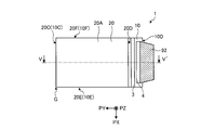
- FIG. 1 is a perspective view illustrating an example of the display device according to the present embodiment.
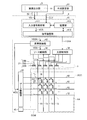
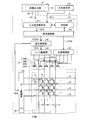
- FIG. 2 is a block diagram illustrating the display device according to the first embodiment.
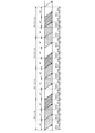
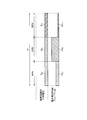
- FIG. 3 is a timing chart for explaining the timing at which the light source emits light in the field sequential system according to the first embodiment.
- FIG. 4 is an explanatory diagram showing the relationship between the voltage applied to the pixel electrode and the scattering state of the pixel.
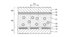
- FIG. 5 is a cross-sectional view illustrating an example of a cross section of the display device of FIG.
- FIG. 6 is a plan view showing a plane of the display device of FIG.
- FIG. 7 is an enlarged sectional view in which the liquid crystal layer portion of FIG. 5 is enlarged.
- FIG. 8 is a cross-sectional view for explaining a non-scattering state in the liquid crystal layer.
- FIG. 9 is a cross-sectional view for explaining a scattering state in the liquid crystal layer.
- FIG. 10 is a plan view showing a pixel.
- FIG. 11 is a sectional view taken along line B1-B2 of FIG.
- FIG. 12 is a conceptual diagram of a reproduction HSV color space that can be reproduced by the display device of the present embodiment.
- FIG. 13 is a conceptual diagram showing the relationship between hue and saturation in the reproduction HSV color space.
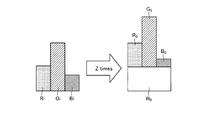
- FIG. 14 is a diagram illustrating an increase in luminance due to signal processing from an input signal value to an output signal value.
- FIG. 15 is a diagram illustrating an example in which the expansion coefficient is always constant and does not change in response to a change in saturation.
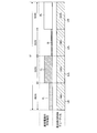
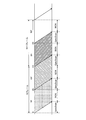
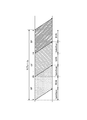
- FIG. 16 is an example of the voltage applied to the pixel electrode and the PWM duty ratio of the light emitting unit during one frame period in one pixel of the first embodiment.
- FIG. 17 is a diagram illustrating an example in which the expansion coefficient changes with a change in saturation.
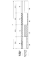
- FIG. 18 is an example of the voltage applied to the pixel electrode and the PWM duty ratio of the light emitting unit during one frame period in one pixel of the second embodiment.
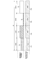
- FIG. 19 is an example of the voltage applied to the pixel electrode and the PWM duty ratio of the light emitting unit during one frame period in one pixel of the third embodiment.
- FIG. 16 is an example of the voltage applied to the pixel electrode and the PWM duty ratio of the light emitting unit during one frame period in one pixel of the first embodiment.
- FIG. 17 is a diagram illustrating an example in which the expansion coefficient changes with a change in saturation.
- FIG. 20 is an example of the voltage applied to the pixel electrode and the PWM duty ratio of the light emitting unit during one frame period in one pixel of the fourth embodiment.
- FIG. 21 is an example of the voltage applied to the pixel electrode and the light emission intensity of the light emitting unit during one frame in one pixel of the fifth embodiment.
- FIG. 22 is an example of the temperature characteristics of the light emitting body in the sixth embodiment.
- FIG. 23 is an example of the voltage applied to the pixel electrode and the PWM duty ratio of the light emitting unit during one frame period in one pixel of the sixth embodiment.
- FIG. 24 is a block diagram illustrating a display device according to the seventh embodiment.
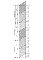
- FIG. 25 is a timing chart illustrating the timing at which the light source emits light in the field sequential system according to the eighth embodiment.
- FIG. 26 is a timing chart illustrating the timing at which the light source emits light in the field sequential method according to the first modification of the eighth embodiment.
- FIG. 27 is a timing chart for explaining the timing at which the light source emits light in the field sequential method according to the second modification of the eighth embodiment.
- FIG. 28 is a timing chart illustrating timings at which the light sources emit light in the field sequential system according to the third modification of the eighth embodiment.
- FIG. 29 is a block diagram illustrating a display device according to the ninth embodiment.
- FIG. 30 is a timing chart illustrating the timing at which the light source emits light in the field sequential system according to the tenth embodiment.
- FIG. 31 is a diagram illustrating an increase in luminance due to signal processing from an input signal value to an output signal value in the tenth embodiment.
- FIG. 32 is an example of the voltage applied to the pixel electrode and the PWM duty ratio of the light emitting unit during one frame in one pixel of the tenth embodiment.
- FIG. 33 is an example of the voltage applied to the pixel electrode and the PWM duty ratio of the light emitting unit during one frame period in one pixel of the first modification of the tenth embodiment.
- FIG. 34 is an example of the applied voltage of the pixel electrode and the PWM duty ratio of the light emitting unit during one frame period in one pixel of Modification 2 of Embodiment 10.
- FIG. 35 is an example of the voltage applied to the pixel electrode and the PWM duty ratio of the light emitting unit during one frame period in one pixel of the third modification of the tenth embodiment.
- FIG. 36 is an example of the voltage applied to the pixel electrode and the PWM duty ratio of the light emitting unit during one frame period in one pixel of Modification Example 4 of Embodiment 10.
- FIG. 1 is a perspective view illustrating an example of the display device according to the present embodiment.
- FIG. 2 is a block diagram illustrating the display device of FIG.
- FIG. 3 is a timing chart illustrating the timing at which the light source emits light in the field sequential method.
- the display device 1 includes a display panel 2, a side light source device 3, a drive circuit 4, and an external light setting unit 61.
- one direction of the plane of the display panel 2 is defined as a PX direction
- a direction orthogonal to the PX direction is defined as a PY direction
- a direction orthogonal to the PX-PY plane is defined as a PZ direction.
- the display panel 2 includes a first light-transmitting substrate 10, a second light-transmitting substrate 20, and a liquid crystal layer 50 (see FIG. 5).
- the second light-transmitting substrate 20 faces in a direction perpendicular to the surface of the first light-transmitting substrate 10 (PZ direction shown in FIG. 1).
- the first light-transmitting substrate 10, the second light-transmitting substrate 20, and the sealing portion 19 seal a polymer-dispersed liquid crystal described later.
- a display area AA In the display area AA, a plurality of pixels Pix are arranged in a matrix.
- a row refers to a pixel row having m pixels Pix arranged in one direction.
- a column refers to a pixel column having n pixels Pix arranged in a direction orthogonal to the direction in which the rows are arranged. The values of m and n are determined according to the vertical display resolution and the horizontal display resolution.
- a plurality of scanning lines 12 are wired for each row, and a plurality of signal lines 13 are wired for each column.
- the side light source device 3 includes a plurality of light emitting units 31. As shown in FIG. 2, the light source control unit 32 is included in the drive circuit 4. The light source control unit 32 may be a circuit different from the circuit of the drive circuit 4. The light emitting unit 31 and the light source control unit 32 are electrically connected by wiring in the first translucent substrate 10.
- the external light setting unit 61 is a visible light sensor, and the visible light sensor detects, for example, the external light 69 of the external light source Q, and outputs information on tristimulus values obtained by spectrally separating the external light 69 according to the wavelength. It is generated as an information signal ELV.
- the external light setting unit 61 transmits the generated external light information signal ELV to the drive circuit 4.
- the external light setting section 61 is fixed to the surface of the first light transmitting substrate 10.
- the external light setting unit 61 is not limited as long as it can detect the external light 69 around the display panel 2.
- the external light setting unit 61 is not limited to the visible light sensor, and may be a setting switch for external light.
- the external light setting switch generates a signal ELV of the external light information based on a set value of the external light information preset by the observer according to the visible light of the external light 69.
- the setting switch of the outside light includes a sunny daylight mode (first environment mode), a cloudy daylight mode (second environment mode), an indoor use mode (third environment mode), and a night use mode (fourth environment mode).
- set values of external light tristimulus values are defined.
- the external light setting unit 61 transmits the generated external light information signal ELV to the drive circuit 4.
- the external light setting unit 61 is an external light setting switch
- the position to which the external light setting switch is fixed is not limited as long as the signal ELV of the external light information can be transmitted to the drive circuit 4.
- the drive circuit 4 is fixed to the surface of the first light-transmitting substrate 10.
- the drive circuit 4 includes an analysis unit 41, a pixel control unit 42, a gate drive unit 43, a source drive unit 44, and a common potential drive unit 45.
- the first light-transmitting substrate 10 has an area in the XY plane larger than that of the second light-transmitting substrate 20, and the driving circuit 4 is provided on the projecting portion of the first light-transmitting substrate 10 exposed from the second light-transmitting substrate 20. Is provided.
- An input signal (such as an RGB signal) VS is input to the analysis unit 41 from the image output unit 91 of the external higher-level control unit 9 via the flexible board 92.
- the analysis unit 41 includes an input signal analysis unit 411, a storage unit 412, and a signal adjustment unit 413.
- the input signal analyzer 411 generates a second input signal VCS based on a first input signal VS input from outside.
- the second input signal VCS is a signal that determines what gradation value is given to each pixel Pix of the display panel 2 based on the first input signal VS.
- the second input signal VCS is a signal including gradation information on the gradation value of each pixel Pix.
- the signal ELV of the external light information from the external light setting unit 61 described above is input to the input signal analyzing unit 411.
- the input signal analyzer 411 generates a second input signal VCS corresponding to the signal ELV of the external light information, as described later.
- the signal adjustment unit 413 generates the third input signal VCSA from the second input signal VCS.
- the signal adjustment unit 413 sends the third input signal VCSA to the pixel control unit 42, and sends the light source control signal LCSA to the light source control unit 32.
- the light source control signal LCSA is, for example, a signal including information on the light amount of the light emitting unit 31 set according to the input gradation value to the pixel Pix. For example, when a dark image is displayed, the light amount of the light emitting unit 31 is set to be small. When a bright image is displayed, the light amount of the light emitting unit 31 is set to be large.
- the pixel control unit 42 generates the horizontal drive signal HDS and the vertical drive signal VDS based on the third input signal VCSA.
- the horizontal driving signal HDS and the vertical driving signal VDS are generated for each color in which the light emitting unit 31 can emit light.
- the gate driving unit 43 sequentially selects the scanning lines 12 of the display panel 2 within one vertical scanning period based on the horizontal driving signal HDS.
- the order of selecting the scanning lines 12 is arbitrary.
- the source driver 44 supplies a gradation signal corresponding to the output gradation value of each pixel Pix to each signal line 13 of the display panel 2 within one horizontal scanning period based on the vertical drive signal VDS.
- the display panel 2 is an active matrix type panel. Therefore, it has a signal (source) line 13 extending in the PY direction and a scanning (gate) line 12 extending in the PX direction in a plan view, and the switching element Tr is provided at the intersection of the signal line 13 and the scanning line 12. Having.
- a thin film transistor is used as the switching element Tr.
- a bottom-gate transistor or a top-gate transistor may be used.
- a single gate thin film transistor is illustrated as the switching element Tr, a double gate transistor may be used.
- One of the source electrode and the drain electrode of the switching element Tr is connected to the signal line 13, the gate electrode is connected to the scanning line 12, and the other of the source electrode and the drain electrode is connected to one end of the liquid crystal capacitor LC. .
- One end of the liquid crystal capacitor LC is connected to the switching element Tr via the pixel electrode 16, and the other end is connected to the common potential COM via the common electrode 22.
- the common potential COM is supplied from the common potential driving unit 45.
- the light emitting unit 31 includes a first color (for example, red) light emitter 33R, a second color (for example, green) light emitter 33G, and a third color (for example, blue) light emitter 33B.
- the light source control unit 32 controls the first color light emitter 33R, the second color light emitter 33G, and the third color light emitter 33B to emit light in a time sharing manner based on the light source control signal LCSA.
- the first color luminous body 33R, the second color luminous body 33G, and the third color luminous body 33B are driven by the field sequential method.
- the first color light-emitting body 33R emits light in the first color light-emitting period RON, and is selected within one vertical scanning period GateScan.
- the pixel Pix scatters light for display.
- the entire display panel 2 if a gradation signal corresponding to the output gradation value of each pixel Pix is supplied to each signal line 13 to the pixel Pix selected within one vertical scan period GateScan, the first pixel is selected. In the color light emission period RON, only the first color is lit.
- the light emitter 33G of the second color emits light in the light emission period GON of the second color
- the pixel Pix selected within one vertical scanning period GateScan emits light. Is scattered and displayed.
- the entire display panel 2 if a gradation signal corresponding to the output gradation value of each pixel Pix is supplied to each signal line 13 to the pixel Pix selected within one vertical scan period GateScan, the second During the color light emission period GON, only the second color is lit.
- the third color light emitting body 33B emits light in the third color light emission period BON, and the pixel Pix selected within one vertical scanning period GateScan emits light. Display by scattering.
- the third In the color light emission period BON only the third color is lit.
- the first color light emitting body 33R, the second color light emitting body 33G, and the third color light emitting body 33B simultaneously emit light in the fourth color light emitting period WON.
- the pixel Pix selected during one vertical scan period GateScan scatters light to display.
- the fourth In the color light emission period WON only the fourth color is lit.
- the light emission period RON of the first color, the light emission period GON of the second color, the light emission period BON of the third color, and the period WON of the fourth color are sequentially processed in one frame period. .
- the human eye has a temporal resolution limitation, and an afterimage is generated. Therefore, a combined image of four colors is recognized during one frame (1F).
- a color filter can be dispensed with and the absorption loss in the color filter is reduced, so that a high transmittance can be realized.
- one pixel is formed by subpixels obtained by dividing the pixel Pix for each of the first color, the second color, and the third color, whereas in the field sequential method, such subpixel division is not required. Since it is good, it is easy to increase the resolution.
- FIG. 4 is an explanatory diagram showing the relationship between the voltage applied to the pixel electrode and the scattering state of the pixel.
- FIG. 5 is a cross-sectional view illustrating an example of a cross section of the display device of FIG.
- FIG. 6 is a plan view showing a plane of the display device of FIG.
- FIG. 5 is a sectional view taken along the line V-V 'of FIG.
- FIG. 7 is an enlarged sectional view in which the liquid crystal layer portion of FIG. 5 is enlarged.
- FIG. 8 is a cross-sectional view for explaining a non-scattering state in the liquid crystal layer.
- FIG. 9 is a cross-sectional view for explaining a scattering state in the liquid crystal layer.
- a gradation signal corresponding to the output gradation value of each pixel Pix is supplied to the signal line 13 to the pixel Pix selected within one vertical scanning period GateScan, the pixel electrode is selected according to the gradation signal.
- the applied voltage to 16 changes.
- the voltage applied to the pixel electrode 16 changes, the voltage between the pixel electrode 16 and the common electrode 22 changes.
- the scattering state of the liquid crystal layer 50 for each pixel Pix is controlled according to the voltage applied to the pixel electrode 16, and the scattering ratio in the pixel Pix changes.
- the drive circuit 4 changes the voltage applied to the pixel electrode 16 according to the vertical drive signal VDS in the voltage range Vdr lower than the saturation voltage Vsat.
- the first light-transmitting substrate 10 includes a first main surface 10A, a second main surface 10B, a first side surface 10C, a second side surface 10D, a third side surface 10E, and a fourth side surface 10F. Is provided.
- the first main surface 10A and the second main surface 10B are parallel planes.
- the first side surface 10C and the second side surface 10D are parallel planes.
- the third side face 10E and the fourth side face 10F are parallel planes.
- the second translucent substrate 20 includes a first main surface 20A, a second main surface 20B, a first side surface 20C, a second side surface 20D, a third side surface 20E, and a fourth side surface 20F. Is provided.
- the first main surface 20A and the second main surface 20B are parallel planes.
- the first side surface 20C and the second side surface 20D are parallel planes.
- the third side surface 20E and the fourth side surface 20F are parallel planes.
- the light emitting unit 31 faces the second side surface 20 ⁇ / b> D of the second translucent substrate 20. As illustrated in FIG. 5, the light emitting unit 31 irradiates the second side surface 20D of the second translucent substrate 20 with the light source light L.
- the second side surface 20D of the second light-transmitting substrate 20 facing the light emitting unit 31 is a light incident surface.
- the light source light L emitted from the light emitting unit 31 is reflected by the first main surface 10A of the first light-transmitting substrate 10 and the first main surface 20A of the second light-transmitting substrate 20. , Propagating away from the second side surface 20D.
- the light source light L travels from the first principal surface 10A of the first translucent substrate 10 or the first principal surface 20A of the second translucent substrate 20 to the outside, it proceeds from a medium having a large refractive index to a medium having a small refractive index.
- the incident angle at which the light source light L enters the first principal surface 10A of the first translucent substrate 10 or the first principal surface 20A of the second translucent substrate 20 is larger than the critical angle, the light source The light L is totally reflected by the first main surface 10A of the first light-transmitting substrate 10 or the first main surface 20A of the second light-transmitting substrate 20.
- the light source light L that has propagated inside the first light-transmitting substrate 10 and the second light-transmitting substrate 20 is scattered by a pixel Pix having a scattered liquid crystal, and the scattered light
- the incident angle becomes an angle smaller than the critical angle
- the radiated lights 68 and 68A are respectively transmitted from the first main surface 20A of the second light-transmitting substrate 20 and the first main surface 10A of the first light-transmitting substrate 10 to the outside.
- the emitted light 68, 68A radiated to the outside from the first main surface 20A of the second light-transmitting substrate 20 and the first main surface 10A of the first light-transmitting substrate 10, respectively, is observed by an observer.
- the polymer-dispersed liquid crystal in a scattering state and the polymer-dispersed liquid crystal in a non-scattered state will be described with reference to FIGS.
- the first translucent substrate 10 is provided with a first alignment film 55.
- a second alignment film 56 is provided on the second translucent substrate 20.
- the first alignment film 55 and the second alignment film 56 are, for example, vertical alignment films.
- the solution containing the liquid crystal and the monomer is sealed between the first light-transmitting substrate 10 and the second light-transmitting substrate 20.
- the monomer is polymerized by ultraviolet light or heat to form the bulk 51.
- the liquid crystal layer 50 having the reverse mode polymer dispersed liquid crystal in which the liquid crystal is dispersed in the gaps of the polymer network formed in a network is formed.
- the liquid crystal layer 50 has the bulk 51 formed of the polymer and the plurality of fine particles 52 dispersed in the bulk 51.
- the fine particles 52 are formed of liquid crystal.
- the bulk 51 and the fine particles 52 each have optical anisotropy.
- the orientation of the liquid crystal contained in the fine particles 52 is controlled by the voltage difference between the pixel electrode 16 and the common electrode 22.
- the orientation of the liquid crystal changes depending on the voltage applied to the pixel electrode 16.
- the degree of scattering of light passing through the pixel Pix changes.
- the directions of the optical axis Ax1 of the bulk 51 and the optical axis Ax2 of the fine particles 52 are equal to each other.
- the optical axis Ax2 of the fine particles 52 is parallel to the PZ direction of the liquid crystal layer 50.
- the optical axis Ax1 of the bulk 51 is parallel to the PZ direction of the liquid crystal layer 50 regardless of the presence or absence of a voltage.
- the ordinary light refractive index of the bulk 51 and the fine particles 52 are equal to each other.
- the refractive index difference between the bulk 51 and the fine particles 52 becomes zero in all directions.
- the liquid crystal layer 50 is in a non-scattering state in which the light source light L is not scattered.
- the light source light L propagates in a direction away from the light emitting unit 31 while being reflected by the first main surface 10A of the first light-transmitting substrate 10 and the first main surface 20A of the second light-transmitting substrate 20.
- the background from the first main surface 10A of the first light-transmitting substrate 10 to the first main surface 20A of the second light-transmitting substrate 20 is visually recognized.
- the background on the first main surface 10A side of the first light transmissive substrate 10 is visible from the first main surface 20A of the second light transmissive substrate 20.
- the optical axis Ax2 of the fine particles 52 is inclined by the electric field generated between the pixel electrode 16 and the common electrode 22. Become. Since the optical axis Ax1 of the bulk 51 does not change due to the electric field, the directions of the optical axis Ax1 of the bulk 51 and the optical axis Ax2 of the fine particles 52 are different from each other. In the pixel Pix having the pixel electrode 16 to which the voltage is applied, the light source light L is scattered.
- a part of the scattered light source light L is emitted to the outside from the first main surface 10A of the first light-transmitting substrate 10 or the first main surface 20A of the second light-transmitting substrate 20. Observed by the observer.
- the background from the first main surface 10A of the first light-transmitting substrate 10 to the first main surface 20A of the second light-transmitting substrate 20 is visually recognized. 2.
- the background on the first main surface 10A side of the first light transmissive substrate 10 from the first main surface 20A of the light transmissive substrate 20 is visible.
- the display device 1 of the present embodiment applies a voltage to the pixel electrode 16 of the pixel Pix on which an image is displayed, and outputs the voltage to the third input signal VCSA. Based images are viewed with the background.
- the display device 1 of the present embodiment displays an image by superimposing the image on the background by combining the emitted light 68 or the emitted light 68A with the background.
- FIG. 10 is a plan view showing a pixel.
- FIG. 11 is a sectional view taken along the line XI-XI 'of FIG.
- a plurality of signal lines 13 and a plurality of scanning lines 12 are provided on the first light-transmitting substrate 10 in a lattice shape in plan view.
- a region surrounded by adjacent scanning lines 12 and adjacent signal lines 13 is a pixel Pix.
- the pixel Pix is provided with a pixel electrode 16 and a switching element Tr.
- the switching element Tr is a bottom-gate thin film transistor.
- the switching element Tr has a semiconductor layer 15 that overlaps with the gate electrode 12G electrically connected to the scanning line 12 in plan view.
- the scanning line 12 is a wiring made of a metal such as molybdenum (Mo) or aluminum (Al), a laminate thereof, or an alloy thereof, and the signal line 13 is a wiring made of a metal or an alloy such as aluminum.
- the semiconductor layer 15 is provided so as not to protrude from the gate electrode 12G in plan view. Thereby, the light source light L traveling from the gate electrode 12G side toward the semiconductor layer 15 is reflected, and light leakage hardly occurs in the semiconductor layer 15.
- the source electrode 13S electrically connected to the signal line 13 overlaps with one end of the semiconductor layer 15 in plan view.
- a drain electrode 14D is provided at a position adjacent to the source electrode 13S with the central portion of the semiconductor layer 15 interposed therebetween in a plan view.
- the drain electrode 14D overlaps with the other end of the semiconductor layer 15 in a plan view.
- a portion that does not overlap with the source electrode 13S and the drain electrode 14D functions as a channel of the switching element Tr.
- the conductive wiring 14 connected to the drain electrode 14D is electrically connected to the pixel electrode 16 through a through hole SH.
- the first light-transmitting substrate 10 has a first base material 11 formed of, for example, glass.
- the first base material 11 may be a resin such as polyethylene terephthalate, as long as it has translucency.
- the first insulating layer 17a is provided on the first base material 11, and the scanning lines 12 and the gate electrodes 12G are provided on the first insulating layer 17a. Further, a second insulating layer 17b is provided so as to cover the scanning lines 12.
- the first insulating layer 17a and the second insulating layer 17b are formed of, for example, a transparent inorganic insulating member such as silicon nitride.
- the semiconductor layer 15 is stacked on the second insulating layer 17b.
- the semiconductor layer 15 is formed of, for example, amorphous silicon, but may be formed of polysilicon or an oxide semiconductor.
- a source electrode 13S and a signal line 13 covering a part of the semiconductor layer 15, a drain electrode 14D covering a part of the semiconductor layer 15, and a conductive wiring 14 are provided.
- the drain electrode 14D is formed of the same material as the signal line 13.
- a third insulating layer 17c is provided on the semiconductor layer 15, the signal line 13, and the drain electrode 14D.
- the third insulating layer 17c is formed of, for example, a transparent inorganic insulating member such as silicon nitride.
- the pixel electrode 16 is provided on the third insulating layer 17c.
- the pixel electrode 16 is formed of a light-transmitting conductive member such as ITO (Indium Tin Oxide).
- the pixel electrode 16 is electrically connected to the conductive wiring 14 and the drain electrode 14D via a contact hole provided in the third insulating layer 17c.
- a first alignment film 55 is provided on the pixel electrode 16.
- the second translucent substrate 20 has a second base member 21 made of, for example, glass.
- the second base material 21 may be a resin such as polyethylene terephthalate, as long as it has translucency.
- the common electrode 22 is provided on the second base 21.
- the common electrode 22 is formed of a translucent conductive member such as ITO.
- a second alignment film 56 is provided on the surface of the common electrode 22, a second alignment film 56 is provided.
- FIG. 12 is a conceptual diagram of a reproduction HSV color space that can be reproduced by the display device of the present embodiment.
- FIG. 13 is a conceptual diagram showing the relationship between hue and saturation in the reproduction HSV color space.
- the input signal analyzer 411 receives a first input signal VS, which is information on an image to be displayed from the outside.
- the first input signal VS includes information on an image (color) to be displayed at that position for each pixel in the first input signal VS.
- the input signal analysis unit 411 shown in FIG. 2 generates the RGBW signal by processing the first input signal VS, and outputs the RGBW signal to the signal adjustment unit 413.
- the display device 1 can extend the dynamic range of lightness in the HSV color space (reproduced HSV color space) shown in FIG. 12 by including the light emission period WON of the fourth color.
- the signal adjustment unit 413 reads the expansion coefficient Z corresponding to the signal ELV of the external light information from the storage unit 412.
- the expansion coefficient Z is one or more coefficients as described later.
- the input signal analysis unit 411 performs the HSV conversion on the RGB signals [R i , G i , B i ] of each pixel Pix included in the first input signal VS illustrated in FIG.
- An RGBW signal [R 0 , G 0 , B 0 , W 0 ] of each pixel is calculated based on S and the expansion coefficient Z.
- the saturation S can take a value from 0 to 1
- the brightness V (S) can take a value from 0 to (2 n -1)
- n is the number of display gradation bits.
- Max is included in the first input signal VS, and the first color gradation value R i , the second color gradation value G i, and the third color gradation value to be displayed on one pixel Pix. of B i, is the maximum value.
- the gradation value G i of the second color is Max.
- Min is included in the first input signal VS and is displayed on one pixel Pix.
- the first color tone value R i , the second color tone value G i, and the third color tone value B are displayed.
- i is the minimum value.
- the tone value B i of the third color is Min.
- Hue H is represented by 0 ° to 360 ° as shown in FIG. From 0 ° to 360 °, red (Red), yellow (Yellow), green (Green), cyan (Cyan), blue (Blue), magenta (Magenta), and red.
- the expansion coefficient Z is stored in the storage unit 412. As described above, when the signal ELV of the external light information is equal to or larger than the threshold, or in the sunlight clear mode (first environment mode), the cloudy daylight mode (second environment mode), and the indoor use mode (third environment mode) ), The expansion coefficient Z is larger than 1 and is a constant value regardless of the magnitude of the saturation S. For example, as shown in FIG. 15, the expansion coefficient Z is 2 regardless of the magnitude of the saturation S.
- the expansion coefficient Z is 1.
- the extension coefficient Z becomes larger than 1.
- the storage unit 412 stores the luminance increase ratio of the fourth color in the light emitting unit 31.
- the luminance increase ratio ⁇ is the luminance obtained by simultaneously driving the first color luminous body 33R, the second color luminous body 33G, and the third color luminous body 33B at a predetermined PWM duty ratio. This is a value obtained by dividing the average of the brightness of each of the light emitters 33R of one color, the light emitter 33G of the second color, and the light emitter 33B of the third color independently driven.
- the input signal analysis unit 411 calculates the RGBW signal [R 0 , G 0 , B 0 , W 0 ] of each pixel by the following equations (1) to (4). ).
- R 0 Z ⁇ R i - ⁇ ⁇ W 0 (1)
- G 0 Z ⁇ G i - ⁇ ⁇ W 0 (2)
- B 0 Z ⁇ B i - ⁇ ⁇ W 0 (3)
- W 0 Min ⁇ Z / ⁇ (4)
- the first color tone value R 0 , the second color tone value G 0 , and the third color tone value B 0 included in the second input signal VCS are one or more expansion coefficients.
- Z, contained in the first input signal VS, the first color tone value R i, is determined based on a function of the second color gradation values G i, and the third color gradation values B i of the.
- tone value W 0 of the fourth color included in the second input signal VCS is determined by the expansion coefficient Z, the luminance increase ratio ⁇ of the fourth color in the light emitting unit 31, and the first color of the first color included in the first input signal VS.
- tone value R i is determined based on a function of the minimum value Min of the second color gradation values G i, and the third color gradation values B i of the.
- the gradation value R 0 of the first color, the gradation value G 0 of the second color, and the gradation value B 0 of the third color have the gradation value W 0 of the fourth color by the expansion coefficient Z,
- the first color gradation value R i , the second color gradation value G i , and the third color gradation value Bi are more easily recognized than displayed as they are.
- the input signal analysis unit 411 converts the RGB signals [R i , G i , B i ] of each pixel included in the first input signal VS shown in FIG.
- the RGBW signal [R 0 , G 0 , B 0 , W 0 ] may be calculated.
- the signal adjustment unit 413 generates the third input signal VCSA from the second input signal VCS.
- the third input signal VCSA includes gray scale values [R 1 , G 1 , B 1 , W 1 ] proportional to the gray scale values [R 0 , G 0 , B 0 , W 0 ] of the second input signal VCS. I do.
- this is an example of the voltage applied to the pixel electrode and the PWM duty ratio of the light emitting unit during one frame.
- the PWM duty ratios of the light emitting units 31 in the first color light emitting period RON, the second color light emitting period GON, the third color light emitting period BON, and the fourth color light emitting period WON are the same. .
- the first color to be displayed in one pixel Pix, the second color, the maximum gradation of the third color is a gray scale value G 1.
- Voltage applied to the pixel electrode 16 by the gradation value G 1 is smaller than the saturation voltage Vsat of change in the scattering ratio of the pixel Pix is reduced according to the increase of the applied voltage. For this reason, the driving circuit 4 is not restricted by the output range, and the driving circuit 4 can apply a voltage to the pixel electrode 16 below the upper limit.
- the signal adjustment unit 413 generates a light source control signal LCSA. Based on the tone values [LR 1 , LG 1 , LB 1 , LW 1 ] of the light source control signal LCSA, the first color luminous body 33 R, the second color luminous body 33 G, and the third color luminous body 33 B are formed. It is driven at a PWM duty ratio of 100%.
- the voltages applied to the pixel electrodes in the first color light emission period RON, the second color light emission period GON, the third color light emission period BON, and the fourth color light emission period WON are the first color gradation value R 0 , tone values of two colors G 0, is proportional to the third-color gradation values B 0 and the fourth color gradation values W of.
- the drive circuit 4 includes, based on the RGB signals [R i , G i , B i ] of the first, second, and third colors included in the input first input signal VS and displayed on each pixel. Convert to the second input signal VCS.
- the gradation values [R 0 , G 0 , B 0 , W 0 ] of the second input signal VCS are the gradation values of the first color, the second color, the third color, and the fourth color, respectively.
- the fourth color having a higher luminance than the first color, the second color, and the third color emits light, so that the visibility of the display device 1 is improved.
- FIG. 17 is a diagram illustrating an example in which the expansion coefficient changes with a change in saturation.
- the expansion coefficient Z is set to be small for a signal value having a large saturation S, and the expansion coefficient Z is set to be large for a signal value having a small saturation S. That is, as the saturation S increases, the extension coefficient Z decreases.
- V (S) Vmax (S) / V (S) (5)
- the input signal analysis unit 411 stores the value of the maximum value Vmax (S) of lightness at the coordinates (value) of saturation and hue shown in FIG. 13 in the storage unit 412.
- the saturation S is calculated by the following equation (6).
- V (S) (Max / 255) 2.2 (7)
- the display device 1 and the driving method thereof use the expansion coefficient Z as a function of Max and Min of the input signal as shown in the following equation (5), thereby suppressing the image quality deterioration. Brightness can be improved.
- FIG. 18 is an example of the voltage applied to the pixel electrode and the PWM duty ratio of the light emitting unit during one frame period in one pixel of the second embodiment.
- the same components as those described in the above-described embodiment are denoted by the same reference numerals, and redundant description will be omitted.
- the storage unit 412 stores the luminance increase ratio of the fourth color in the light emitting unit 31.
- the brightness increase ratio ⁇ is obtained by changing the brightness of the fourth color light emitting body 33W at the predetermined PWM duty ratio to the first color light emitting body 33R and the second color light emitting body 33G at the same PWM duty ratio. And a value obtained by dividing the average of the luminances of the light emitting bodies 33B of the third color independently driven.
- the maximum value Vmax (S) of the lightness using the saturation S as a variable in the HSV color space expanded by adding the fourth color is stored in the storage unit 412, for example, as a kind of lookup. • Stored as a table.
- the maximum value Vmax (S) of lightness using the saturation S in the enlarged HSV color space as a variable is obtained by the input signal analysis unit 411 each time.
- the input signal analysis unit 411 calculates the saturation S and the brightness V (S) of the pixel Pix. The input signal analysis unit 411 performs this processing for all the pixels Pix.
- the input signal analysis unit 411 calculates the expansion coefficient ⁇ (S) based on Vmax (S) / V (S) calculated for each pixel Pix based on the following equation (8).
- the storage unit 412 stores a limit value ⁇ (Limit value) in advance.
- the percentage of all pixels whose expanded lightness value obtained from the product of the lightness V (S) and the expansion coefficient ⁇ (S) exceeds the maximum value Vmax (S) is equal to or less than the limit value ⁇ (Limit value).
- Such an expansion coefficient ⁇ (S) is determined as the expansion coefficient Z.
- the input signal analyzing unit 411 determines the tone value W 0.
- the input signal analysis unit 411 calculates the tone value W 0 in all the pixels Pix.
- the input signal analysis unit 411 calculates the gradation values R 0, G 0, and B 0 for each pixel Pix based on the above-described equations (1), (2), and (3).
- the PWM duty ratio of the light emitting section 31 in the first color light emitting period RON, the second color light emitting period GON, the third color light emitting period BON, and the fourth color light emitting period WON is (1 / Z) times. I do.
- the signal adjustment unit 413 generates the light source control signal LCSA so that (1 / Z) times becomes the PWM duty ratio 70%.
- the drive circuit 4 Based on the signal values [LR 2 , LG 2 , LB 2 , LW 2 ] of the light source control signal LCSA, the drive circuit 4 generates the first color luminous body 33 R, the second color luminous body 33 G, and the third color luminous body 33 G.
- the light emitter 33B is driven at a PWM duty ratio of 70%.
- the signal adjustment unit 413 generates the third input signal VCSA from the second input signal VCS.
- the gradation value [R 0 , G 0 , B 0 , W 0 ] of the second input signal VCS is equal to the gradation value [R 2 , G 2 , B 2 , W 2 ].
- the light emitting unit 31 is driven at a PWM duty ratio proportional to the reciprocal of the expansion coefficient Z.
- the driving circuit 4 drives the first color luminous body 33R, the second color luminous body 33G, and the third color luminous body 33B uniformly lower, so that the power consumption is low.
- FIG. 19 is an example of the voltage applied to the pixel electrode and the PWM duty ratio of the light emitting unit during one frame period in one pixel of the third embodiment.
- the same components as those described in the above-described embodiment are denoted by the same reference numerals, and redundant description will be omitted.
- the PWM duty ratios of the light emitting units 31 in the light emitting period RON of the first color, the light emitting period GON of the second color, the light emitting period BON of the third color, and the light emitting period WON of the fourth color are different.
- the signal adjusting unit 413 specifies a non-zero and minimum gradation value among the gradation values [R 0 , G 0 , B 0 ] and sets the specified gradation value as a reference value.
- the gradation value B0 is the reference value.
- the signal adjustment unit 413 calculates the gradation value [R 3 , G 3 , B 3 , W 3 ] of the third input signal VCSA to be the following value, as shown in the following equation (9). I do.
- the signal adjustment unit 413 generates the light source control signal LCSA based on the gradation value [R 0 , G 0 , B 0 , W 0 ] of the second input signal VCS.
- the signal values [LR 3 , LG 3 , LB 3 , LW 3 ] of the light source control signal LCSA are signal values [LS ⁇ R 0 / B 0 , LS ⁇ G 0 / B 0 , LS ⁇ B 0 / B 0 , LS ⁇ W 0 / B 0 ].
- the drive circuit 4 or the analysis unit 41 generates one gradation value of the first color, the second color, and the third color included in the second input signal VCS and displayed on one pixel Pix. Is selected as the reference value.
- the gradation value R 0 of the first color to be displayed on one pixel Pix included in the second input signal VCS is proportional to a coefficient obtained by dividing by the gradation value B 0 of the reference value.
- the light emitting unit 31 is controlled by the duty ratio of the pulse width modulation to be performed.
- the second-color light emission period GON included in the second input signal VCS, proportional to the coefficient divided by the tone value B 0 of the second color gradation value G 0 is a reference value that is displayed on one pixel Pix
- the light emitting unit 31 is controlled by the duty ratio of the pulse width modulation to be performed.
- the third-color light emission period BON included in the second input signal VCS, proportional to the coefficient divided by the tone value B 0 of the third color gradation value B 0 is a reference value that is displayed on one pixel Pix
- the light emitting unit 31 is controlled by the duty ratio of the pulse width modulation to be performed.
- the gradation value W 0 of the fourth color to be displayed on one pixel Pix included in the second input signal VCS is proportional to a coefficient obtained by dividing by the gradation value B 0 of the reference value.
- the light emitting unit 31 is controlled by the duty ratio of the pulse width modulation to be performed.
- FIG. 20 is an example of the voltage applied to the pixel electrode and the PWM duty ratio of the light emitting unit during one frame period in one pixel of the fourth embodiment.
- the same components as those described in the above-described embodiment are denoted by the same reference numerals, and redundant description will be omitted.
- the PWM duty ratios of the light emitting units 31 in the first color light emitting period RON, the second color light emitting period GON, the third color light emitting period BON, and the fourth color light emitting period WON are different.
- the signal adjustment unit 413 specifies the second gradation value (intermediate gradation value) that is not 0 and is the reference value among the gradation values [R 0 , G 0 , B 0 ].
- the gradation value R0 is the reference value.
- the signal adjustment unit 413 calculates the gradation value [R 4 , G 4 , B 4 , W 4 ] of the third input signal VCSA to be the following value as shown in the following equation (10). I do.
- the signal adjustment unit 413 generates the light source control signal LCSA based on the gradation value [R 0 , G 0 , B 0 , W 0 ] of the second input signal VCS.
- the signal values [LR 4 , LG 4 , LB 4 , LW 4 ] of the light source control signal LCSA are the signal values [LS ⁇ R 0 / R 0 , LS ⁇ G 0 / R 0 , LS ⁇ B 0 / R 0 , LS ⁇ W 0 / R 0 ].
- the drive circuit 4 or the analysis unit 41 generates one gradation value of the first color, the second color, and the third color included in the second input signal VCS and displayed on one pixel Pix. Is selected as the reference value.
- the light emitting period RON of the first color the light emitting period GON of the second color, the light emitting period BON of the third color, and the light emitting period WON of the fourth color
- the light emitting period is constant based on the gradation value R0 of the reference value. Is applied to the pixel electrode 16 which is the first electrode.
- the light emitting unit 31 is controlled by the duty ratio of the pulse width modulation to be performed.
- the second-color light emission period GON included in the second input signal VCS, proportional to the coefficient divided by the tone value R 0 of the second color gradation value G 0 is a reference value that is displayed on one pixel Pix
- the light emitting unit 31 is controlled by the duty ratio of the pulse width modulation to be performed.
- the gradation value B 0 of the third color to be displayed on one pixel Pix included in the second input signal VCS is proportional to a coefficient obtained by dividing by the gradation value R 0 of the reference value.
- the light emitting unit 31 is controlled by the duty ratio of the pulse width modulation to be performed.
- the fourth color light emission period WON included in the second input signal VCS, proportional to the coefficient divided by the tone value R 0 of the 4-color gray scale value W 0 is a reference value that is displayed on one pixel Pix
- the light emitting unit 31 is controlled by the duty ratio of the pulse width modulation to be performed.
- FIG. 21 is an example of the voltage applied to the pixel electrode and the light emission intensity of the light emitting unit during one frame in one pixel of the fifth embodiment.
- the same components as those described in the above-described embodiment are denoted by the same reference numerals, and redundant description will be omitted.
- the PWM duty ratio of the light emitting unit 31 in the first color light emitting period RON, the second color light emitting period GON, the third color light emitting period BON, and the fourth color light emitting period WON is 100%. In each case, the emission intensity is the same at 70%.
- the first color to be displayed in one pixel Pix, the second color, the maximum gradation of the third color is a gray scale value G 1.
- Voltage applied to the pixel electrode 16 by the gradation value G 1 is smaller than the saturation voltage Vsat of change in the scattering ratio of the pixel Pix is reduced according to the increase of the applied voltage. For this reason, the driving circuit 4 is not restricted by the output range, and the driving circuit 4 can apply a voltage to the pixel electrode 16 below the upper limit.
- the signal adjustment unit 413 generates a light source control signal LCSA. Based on the signal values [LR 2 , LG 2 , LB 2 , LW 2 ] of the light source control signal LCSA, the drive circuit 4 generates the first color luminous body 33 R, the second color luminous body 33 G, and the third color luminous body 33 G.
- the light emitter 33B is driven at a PWM duty ratio of 70%.
- the signal adjustment unit 413 generates the third input signal VCSA from the second input signal VCS.
- the third input signal VCSA includes gray scale values [R 5 , G 5 , B 5 , W 5 ] proportional to the gray scale values [R 0 , G 0 , B 0 , W 0 ] of the second input signal VCS. I do.
- the gradation value [R 5 , G 5 , B 5 , W 5 ] is 100/70 times the gradation value [R 0 , G 0 , B 0 , W 0 ].
- the voltages applied to the pixel electrodes in the first color light emission period RON, the second color light emission period GON, the third color light emission period BON, and the fourth color light emission period WON are the first color gradation value R 0 , 2-color gradation value G 0 of proportional to the third-color gradation values B 0 and the fourth color gradation value Wo of.
- FIG. 22 is an example of the temperature characteristics of the light emitting body in the sixth embodiment.
- FIG. 23 is an example of the voltage applied to the pixel electrode and the PWM duty ratio of the light emitting unit during one frame period in one pixel of the sixth embodiment.
- the same components as those described in the above-described embodiment are denoted by the same reference numerals, and redundant description will be omitted.
- the first color luminous body 33R has a different temperature characteristic from the second color luminous body 33G and the third color luminous body 33B.
- the main material of the first color light emitting body 33R is aluminum indium gallium phosphide (AlInGaP), while the main material of the second color light emitting body 33G and the third color light emitting body 33B is gallium nitride ( GaN).
- the signal adjustment unit 413 generates a light source control signal LCSA. Based on the signal value [LR 6 , LG 6 , LB 6 , LW 6 ] of the light source control signal LCSA, the drive circuit 4 switches the first color light emitting body 33 R to the second color light emitting body 33 G and the third color light emitting body 33 G. Is driven with a value having a smaller PWM duty ratio than the light emitting body 33B. For example, the drive circuit 4 drives the light emitter 33R of the first color at a PWM duty ratio of 70%, and drives the light emitter 33G of the second color and the light emitter 33B of the third color at a PWM duty ratio of 100%.
- the signal adjustment unit 413 generates the third input signal VCSA from the second input signal VCS.
- the third input signal VCSA has a gradation value having a relationship represented by the following equations (11) to (14) with respect to the gradation value [R 0 , G 0 , B 0 , W 0 ] of the second input signal VCS. [R 6 , G 6 , B 6 , W 6 ].
- R 6 100/70 ⁇ R 0 (11)
- G 6 G 0 (12)
- B 6 B 0 (13)
- W 6 W 0 (14)
- Tone value R 6 of the first color becomes larger than the gradation value R 0 of the first color
- PWM duty ratio of the first color light emitter 33R is smaller.
- the first color luminous body 33R has a temperature characteristic in which the relative luminous intensity decreases as the heat generation temperature Ta increases, compared to the second color luminous body 33G and the third color luminous body 33B.
- the light emitter 33R of the first color is driven in a state where the PWM duty ratio is multiplied by a smaller coefficient than the light emitter 33G of the second color and the light emitter 33B of the third color. Thereby, the heat generation of the first color light emitting body 33R is suppressed, and a decrease in relative luminous intensity due to a rise in temperature is suppressed.
- FIG. 24 is a block diagram illustrating a display device according to the seventh embodiment.
- the light emitting unit 31 includes a first color light emitter 33R, a second color light emitter 33G, a third color light emitter 33B, and a fourth (for example, white) light emitter 33W.
- a first color light emitter 33R a second color light emitter 33G
- a third color light emitter 33B a third color light emitter 33B
- a fourth (for example, white) light emitter 33W for example, white
- the fourth color light emitting body 33W emits light in the fourth color light emission period WON, and is selected within one vertical scanning period GateScan.
- the pixel Pix scatters light for display.
- the entire display panel 2 if a gradation signal corresponding to the output gradation value of each pixel Pix is supplied to each signal line 13 to the pixel Pix selected within one vertical scan period GateScan, the fourth In the color light emission period WON, only the fourth color is lit.
- the light source control unit 32 time-divides each of the first color light emitter 33R, the second color light emitter 33G, the third color light emitter 33B, and the fourth color light emitter 33W. Is controlled to emit light.
- the first color luminous body 33R, the second color luminous body 33G, the third color luminous body 33B, and the fourth color luminous body 33W are driven by a field sequential method.
- the display device of the seventh embodiment can be applied to the first to sixth embodiments. Further, the display device according to the seventh embodiment can be applied to other embodiments described later.
- FIG. 25 is a timing chart illustrating the timing at which the light source emits light in the field sequential system according to the eighth embodiment.
- the same components as those described in the above-described embodiment are denoted by the same reference numerals, and redundant description will be omitted.
- a period of N frames (first frame period) and a period of N + 1 frames (second frame period) next to the period of N frames are alternately repeated.
- the first subframe RF, the second subframe GF, and the third subframe BF are sequentially processed.
- processing is performed based on the average value of the gradation values B 0 in the period of the N frame and the period of the N + 1 frame.
- the first sub-frame RF, the second sub-frame GF, and the fourth sub-frame WF are sequentially processed.
- the number of the fourth sub-frame WF becomes one in the period of two frames, and the luminance is improved.
- the ratio of the first sub-frame RF, the second sub-frame GF, or the third sub-frame BF in one frame is increased.
- the color development of the first, second, and third colors is improved, and the visibility is improved.
- FIG. 26 is a timing chart illustrating the timing at which the light source emits light in the field sequential method according to the first modification of the eighth embodiment.
- the same components as those described in the above-described embodiment are denoted by the same reference numerals, and redundant description will be omitted.
- the period of N frames and the period of N + 1 frames are alternately and repeatedly processed.
- the first subframe RF, the second subframe GF, and the third subframe BF are sequentially processed.
- FIG. 27 is a timing chart for explaining the timing at which the light source emits light in the field sequential method according to the second modification of the eighth embodiment.
- the same components as those described in the above-described embodiment are denoted by the same reference numerals, and redundant description will be omitted.
- a period of N frames (first frame period), a period of N + 1 frame (second frame period), a period of N + 2 frame (third frame period), and a period of N + 3 frame ( The fourth frame period) is processed, and is repeatedly processed.
- the first subframe RF, the second subframe GF, and the third subframe BF are sequentially processed.
- the fourth subframe WF, the first subframe RF, and the second subframe GF are sequentially processed.
- the same components as those described in the above-described embodiment are denoted by the same reference numerals, and redundant description will be omitted.
- the third sub-frame BF, the fourth sub-frame WF, and the first sub-frame RF are sequentially processed.
- the third subframe BF, the fourth subframe WF, and the first subframe RF are sequentially processed.
- the number of the fourth sub-frames WF becomes three in the period of four frames, and the luminance of the display device 1 is improved.
- the ratio of the first sub-frame RF, the second sub-frame GF, or the third sub-frame BF in one frame increases. As a result, the color development of the first, second, and third colors is improved, and the visibility is improved.
- FIG. 28 is a timing chart illustrating timings at which the light sources emit light in the field sequential system according to the third modification of the eighth embodiment.
- the same components as those described in the above-described embodiment are denoted by the same reference numerals, and redundant description will be omitted.
- a period of N frames (first frame period) and a period of N + 1 frames (second frame) next to the period of N frames are alternately and repeatedly processed.
- the first sub-frame RF and the second sub-frame GF are sequentially processed.
- the third sub-frame BF and the fourth sub-frame WF are sequentially processed.
- the number of the fourth sub-frame WF becomes one in the period of two frames, and the luminance is improved.
- the ratio of the first sub-frame RF, the second sub-frame GF, or the third sub-frame BF in one frame can be increased as compared with the processing shown in FIG. As a result, the color development of the first, second, and third colors is improved, and the visibility is improved.
- FIG. 29 is a block diagram illustrating a display device according to the ninth embodiment. As shown in FIG. 29, the light emitting units 31 and the light emitting units 31A are alternately arranged. The same components as those described in the above-described embodiment are denoted by the same reference numerals, and redundant description will be omitted.
- the light emitting unit 31 includes a light emitter 33R of the first color, a light emitter 33G of the second color, and a light emitter 33B of the third color.
- the light emitting unit 31A includes a first color light emitter 33R, a second color light emitter 33G, and a fourth color light emitter 33W.
- the display device according to the ninth embodiment can be applied to the above-described first to eighth embodiments.
- FIG. 30 is a timing chart illustrating the timing at which the light source emits light in the field sequential system according to the tenth embodiment.
- the display device of the tenth embodiment is the same as the display device of the first embodiment.
- FIG. 31 is a diagram illustrating an increase in luminance due to signal processing from an input signal value to an output signal value in the tenth embodiment.
- FIG. 32 is an example of the voltage applied to the pixel electrode and the PWM duty ratio of the light emitting unit during one frame in one pixel of the tenth embodiment.
- the same components as those described in the above-described embodiment are denoted by the same reference numerals, and redundant description will be omitted.
- the display device 1 repeatedly performs the period of N frames.
- the first sub-frame RF, the second sub-frame GF, and the third sub-frame BF are sequentially processed and repeatedly processed.
- the signal adjustment unit 413 shown in FIG. 3 reads out the expansion coefficient Z corresponding to the signal ELV of the external light information from the storage unit 412 as shown in FIG.
- the expansion coefficient Z is one or more coefficients.
- the expansion coefficient Z is stored in the storage unit 412.
- the expansion coefficient Z is larger than 1 and is a constant value regardless of the magnitude of the saturation S. For example, as shown in FIG. 15, the expansion coefficient Z is 2 regardless of the magnitude of the saturation S.
- the input signal analyzer 411 obtains the RGB signals [R 0 , G 0 , B 0 ] of each pixel in the second input signal VCS from the following equations (15) to (17).
- R 0 Z ⁇ R i
- G 0 Z ⁇ G i
- B 0 Z ⁇ B i (17)
- the signal adjustment unit 413 generates the third input signal VCSA from the second input signal VCS.
- the third input signal VCSA has the same gradation value [R 11 , G 11 , B 11 ] as the gradation value [R 0 , G 0 , B 0 ] of the second input signal VCS.
- the signal adjustment unit 413 generates a light source control signal LCSA. Based on the gradation value [LR 11 , LG 11 , LB 11 ] of the light source control signal LCSA, the first color luminous body 33 R, the second color luminous body 33 G, and the third color luminous body 33 B are subjected to the PWM duty ratio. Drive at 100%.
- the drive circuit 4 includes, based on the RGB signals [R i , G i , B i ] of the first, second, and third colors included in the input first input signal VS and displayed on each pixel. Convert to the second input signal VCS.
- the gradation value [R 0 , G 0 , B 0 , W 0 ] of the second input signal VCS is 1 in the RGB signals [R i , G i , B i ] of the first, second, and third colors.
- FIG. 33 is an example of the voltage applied to the pixel electrode and the PWM duty ratio of the light emitting unit during one frame period in one pixel of the first modification of the tenth embodiment.
- the same components as those described in the above-described embodiment are denoted by the same reference numerals, and redundant description will be omitted.
- the input signal analyzer 411 calculates the expansion coefficient Z as described in the second embodiment.
- the RGB signals [R 0 , G 0 , B 0 ] of each pixel in the second input signal VCS are obtained from the obtained expansion coefficient Z and the above-described equations (8) to (10).
- the signal adjustment unit 413 generates the light source control signal LCSA so that (1 / Z) times becomes the PWM duty ratio 70%. Based on the signal value [LR 12 , LG 12 , LB 12 ] of the light source control signal LCSA, the driving circuit 4 generates the first color light emitter 33R, the second color light emitter 33G, and the third color light emitter 33B. Are driven at a PWM duty ratio of 70%.
- the signal adjustment unit 413 generates the third input signal VCSA from the second input signal VCS.
- the gradation value [R 0 , G 0 , B 0 ] of the second input signal VCS is equal to the gradation value [R 12 , G 12 , B 12 ].
- the light emitting unit 31 is driven at a PWM duty ratio proportional to the reciprocal of the expansion coefficient Z.
- the driving circuit 4 drives the first color luminous body 33R, the second color luminous body 33G, and the third color luminous body 33B uniformly lower, so that the power consumption is low.
- FIG. 34 is an example of the applied voltage of the pixel electrode and the PWM duty ratio of the light emitting unit during one frame period in one pixel of Modification 2 of Embodiment 10.
- the same components as those described in the above-described embodiment are denoted by the same reference numerals, and redundant description will be omitted.
- the signal adjusting unit 413 specifies a non-zero and minimum gradation value among the gradation values [R 0 , G 0 , B 0 ] and sets the specified gradation value as a reference value.
- the gradation value B0 is the reference value.
- the signal adjustment unit 413 calculates the gradation value [R 3 , G 3 , B 3 ] of the third input signal VCSA so as to have the following value.
- the signal adjustment unit 413 generates the light source control signal LCSA based on the gradation value [R 0 , G 0 , B 0 ] of the second input signal VCS. Assuming that the reference PWM duty ratio is LS, the signal values [LR 13 , LG 13 , LB 13 , LW 13 ] of the light source control signal LCSA are the signal values [LS ⁇ R 0 / B 0 , LS ⁇ G 0 / B 0 , LS ⁇ B 0 / B 0 ].
- the drive circuit 4 or the analysis unit 41 generates one gradation value of the first color, the second color, and the third color included in the second input signal VCS and displayed on one pixel Pix. Is selected as the reference value.
- the second-color light emission period GON included in the second input signal VCS, proportional to the coefficient divided by the tone value B 0 of the second color gradation value G 0 is a reference value that is displayed on one pixel Pix
- the light emitting unit 31 is controlled by the duty ratio of the pulse width modulation to be performed.
- the third-color light emission period BON included in the second input signal VCS, proportional to the coefficient divided by the tone value B 0 of the third color gradation value B 0 is a reference value that is displayed on one pixel Pix
- the light emitting unit 31 is controlled by the duty ratio of the pulse width modulation to be performed.
- FIG. 35 is an example of the voltage applied to the pixel electrode and the PWM duty ratio of the light emitting unit during one frame period in one pixel of the third modification of the tenth embodiment.
- the same components as those described in the above-described embodiment are denoted by the same reference numerals, and redundant description will be omitted.
- the signal adjustment unit 413 specifies a second gradation value that is not 0 and is the second gradation value among the gradation values [R 0 , G 0 , B 0 ] and uses the second gradation value as a reference value.
- the gradation value R0 is the reference value.
- the signal adjustment unit 413 calculates the gradation value [R 14 , G 14 , B 14 ] of the third input signal VCSA so as to have the following value.
- the signal adjustment unit 413 generates the light source control signal LCSA based on the gradation value [R 0 , G 0 , B 0 ] of the second input signal VCS.
- the signal values [LR 14 , LG 14 , LB 14 , LW 14 ] of the light source control signal LCSA are signal values [LS ⁇ R 0 / R 0 , LS ⁇ G 0 / R 0 , LS ⁇ B 0 / R 0 , LS ⁇ W 0 / R 0 ].
- the drive circuit 4 or the analysis unit 41 generates one gradation value of the first color, the second color, and the third color included in the second input signal VCS and displayed on one pixel Pix. Is selected as the reference value. Then, in the first color light emission period RON, the second color light emission period GON, and the third color light emission period BON, the pixel electrode which is a constant first electrode based on the above-described reference value gradation value R0. Sixteen applied voltages are applied.
- the light emitting unit 31 is controlled by the duty ratio of the pulse width modulation to be performed.
- the second-color light emission period GON included in the second input signal VCS, proportional to the coefficient divided by the tone value R 0 of the second color gradation value G 0 is a reference value that is displayed on one pixel Pix
- the light emitting unit 31 is controlled by the duty ratio of the pulse width modulation to be performed.
- the gradation value B 0 of the third color to be displayed on one pixel Pix included in the second input signal VCS is proportional to a coefficient obtained by dividing by the gradation value R 0 of the reference value.
- the light emitting unit 31 is controlled by the duty ratio of the pulse width modulation to be performed.
- FIG. 36 is an example of the voltage applied to the pixel electrode and the PWM duty ratio of the light emitting unit during one frame period in one pixel of Modification Example 4 of Embodiment 10.
- the same components as those described in the above-described embodiment are denoted by the same reference numerals, and redundant description will be omitted.
- the period of N frames, the period of N + 1 frames, and the period of N + 2 frames are sequentially processed and repeatedly performed.
- the first sub-frame RF and the second sub-frame GF are sequentially processed.
- the third sub-frame BF and the first sub-frame RF are sequentially processed.
- the second sub-frame GF and the third sub-frame BF are sequentially processed. Compared with the processing shown in FIG. 32, the ratio of the first sub-frame RF, the second sub-frame GF, or the third sub-frame BF in one frame is increased. As a result, the color development of the first, second, and third colors is improved, and the visibility is improved.
- the display panel 2 may be a passive matrix type panel having no switching element.
- the passive matrix panel type panel has a first electrode extending in the PX direction in plan view, a second electrode extending in the PY direction, and wiring electrically connected to the first electrode or the second electrode.
- the first electrode, the second electrode, and the wiring are formed of, for example, ITO.
- the above-described first light-transmitting substrate 10 having the first electrode and the second light-transmitting substrate 20 having the second electrode face each other with the liquid crystal layer 50 interposed therebetween.
- the first alignment film 55 and the second alignment film 56 may each be a horizontal alignment film.
- the first alignment film 55 and the second alignment film 56 may have a function of orienting the monomer in a predetermined direction when polymerizing the monomer. As a result, the monomer becomes a polymer that has been polymerized in a state oriented in a predetermined direction.
- the optical axis Ax1 of the bulk 51 and the light are equal to each other and are orthogonal to the PZ direction.
- the direction perpendicular to the PZ direction corresponds to the PX direction or the PY direction along the side of the first light-transmitting substrate 10 in plan view.
- the first light-transmitting substrate includes a first main surface and a second main surface that is a plane parallel to the first main surface
- the second light-transmitting substrate includes a first main surface and a second main surface that is a plane parallel to the first main surface.
- the light emitting unit is controlled in proportion to the reciprocal of the expansion coefficient, and the first color, the second color, and the third color have the same duty ratio of pulse width modulation, (1) or (1) or (2), wherein an application voltage of the first electrode according to each gradation value of the first color, the second color, and the third color included in the second input signal is applied.
- (4) The light emitting unit is controlled in proportion to the reciprocal of the expansion coefficient, and the first color, the second color, and the third color have the same light emission intensity, (1) or (1) or (2), wherein an application voltage of the first electrode according to each gradation value of the first color, the second color, and the third color included in the second input signal is applied.
- the voltage applied to the first electrode based on the maximum gradation among the first color, the second color, and the third color to be displayed on one pixel included in the second input signal is the first voltage.
- the display device according to (1) or (2). (7) In the emission period of the first color, the duty of pulse width modulation in which the gradation value of the first color to be displayed on one of the pixels included in the second input signal is proportional to a coefficient divided by the reference value
- the light emitting unit is controlled by the ratio
- the duty of pulse width modulation in which the gradation value of the second color to be displayed on one of the pixels included in the second input signal is proportional to a coefficient divided by the reference value
- the light emitting unit is controlled by the ratio
- the duty of pulse width modulation which is included in the second input signal and is proportional to a coefficient obtained by dividing the gradation value of the third color to be displayed on one pixel by the reference value.
- the display device wherein the light emitting unit is controlled by a ratio.
- the reference value is a minimum gradation value of the first color, the second color, and the third color included in the second input signal and displayed on one of the pixels.
- the display device according to (7).
- the display device according to (7). (10) In one of the above (1) to (9), the light emission period of the first color, the light emission period of the second color, and the light emission period of the third color are sequentially processed in one frame period.
- the display device according to the above.
Landscapes
- Physics & Mathematics (AREA)
- Chemical & Material Sciences (AREA)
- Nonlinear Science (AREA)
- General Physics & Mathematics (AREA)
- Crystallography & Structural Chemistry (AREA)
- Engineering & Computer Science (AREA)
- Mathematical Physics (AREA)
- Optics & Photonics (AREA)
- Theoretical Computer Science (AREA)
- Computer Hardware Design (AREA)
- Dispersion Chemistry (AREA)
- Liquid Crystal (AREA)
- Control Of Indicators Other Than Cathode Ray Tubes (AREA)
- Liquid Crystal Display Device Control (AREA)
Abstract
本発明は、表示パネルの一方の面から、反対側の他方の面側の背景を視認可能であって、表示画像の視認性を向上できる表示装置を提供することを目的とする。 本発明の表示装置は、第1透光性基板と第2透光性基板との間に封入される高分子分散型液晶を有する液晶層と、第1透光性基板の側面及び第2透光性基板の側面の少なくとも1つに対向し、フィールドシーケンシャル方式で、第1~4色(R,G,B,W)のいずれかで発光する発光部(31,31A)と、入力される第1入力信号(VS)に含まれ、各画素に表示させる第1~3色(R,G,B)のRGB信号に基づいて、前記第1~3色(R,G,B)及び第4色(W)のそれぞれの階調値を含む第2入力信号(VCS)に変換する駆動部(4)とを含む。
Description
本開示は、表示装置に関する。
特許文献1には、光変調層と光源とを有している表示装置が記載されている。光変調層は、一対の透明基板の間に配置され、所定の屈折率異方性を有するとともに、透明基板に設けられた電極によって生じる電場に対する応答性が異なる複数の光変調素子を備える。光源は、光変調層の側面から光変調層に所定の色の光を入射する。この光変調層は、電場が生じていないときは光源から入射した入射光を透過し、電場が生じているときは入射光を散乱して透明基板に射出する。
特許文献1に記載されている表示装置では、表示の視認性を向上させようとすると、光の散乱割合を大きくする必要がある。このため、光の散乱割合を大きくするには、画素電極へ印加する電圧を高める必要がある。しかしながら、駆動回路の出力範囲の制約により、画素電極へ印加する電圧には上限がある。
本発明の目的は、表示パネルの一方の面から、反対側の他方の面側の背景を視認可能であって、表示パネルに表示する画像の視認性を向上できる表示装置を提供することにある。
一態様に係る表示装置は、第1透光性基板と、前記第1透光性基板と対向する第2透光性基板と、前記第1透光性基板と前記第2透光性基板との間に封入される高分子分散型液晶を有する液晶層と、前記第1透光性基板の側面及び前記第2透光性基板の側面の少なくとも1つに対向する少なくとも1つの発光部と、前記液晶層を挟むように第1電極及び第2電極を備え、フィールドシーケンシャル方式により、前記発光部において、第1色、第2色、第3色及び第4色のいずれかが発光し、入力される第1入力信号に含まれ、各画素に表示させる前記第1色、前記第2色及び前記第3色のRGB信号に基づいて、前記第1色、前記第2色、前記第3色及び前記第4色のそれぞれの階調値を含む第2入力信号に変換する駆動回路と、を含む。
本開示を実施するための形態(実施形態)につき、図面を参照しつつ詳細に説明する。以下の実施形態に記載した内容により本開示が限定されるものではない。また、以下に記載した構成要素には、当業者が容易に想定できるもの、実質的に同一のものが含まれる。さらに、以下に記載した構成要素は適宜組み合わせることが可能である。なお、開示はあくまで一例にすぎず、当業者において、開示の主旨を保っての適宜変更について容易に想到し得るものについては、当然に本開示の範囲に含有されるものである。また、図面は説明をより明確にするため、実際の態様に比べ、各部の幅、厚さ、形状等について模式的に表される場合があるが、あくまで一例であって、本開示の解釈を限定するものではない。また、本明細書と各図において、既出の図に関して前述したものと同様の要素には、同一の符号を付して、詳細な説明を適宜省略することがある。
(実施形態1)
図1は、本実施形態に係る表示装置の一例を表す斜視図である。図2は、図1の表示装置を表すブロック図である。図3は、フィールドシーケンシャル方式において、光源が発光するタイミングを説明するタイミングチャートである。
図1は、本実施形態に係る表示装置の一例を表す斜視図である。図2は、図1の表示装置を表すブロック図である。図3は、フィールドシーケンシャル方式において、光源が発光するタイミングを説明するタイミングチャートである。
図1に示すように、表示装置1は、表示パネル2と、サイド光源装置3と、駆動回路4と、外光設定部61とを有する。ここで、表示パネル2の平面の一方向がPX方向とされ、PX方向と直交する方向がPY方向とされ、PX-PY平面に直交する方向がPZ方向とされている。
表示パネル2は、第1透光性基板10と、第2透光性基板20と、液晶層50(図5参照)とを備えている。第2透光性基板20は、第1透光性基板10の表面に垂直な方向(図1に示すPZ方向)に対向する。液晶層50(図5参照)は、第1透光性基板10と、第2透光性基板20と、封止部19とで、後述する高分子分散型液晶が封止されている。
図1に示すように、表示パネル2において、封止部19の内側が、表示領域AAとなる。表示領域AAには、複数の画素Pixがマトリクス状に配置されている。なお、本開示において、行とは、一方向に配列されるm個の画素Pixを有する画素行をいう。また、列とは、行が配列される方向と直交する方向に配列されるn個の画素Pixを有する画素列をいう。そして、mとnとの値は、垂直方向の表示解像度と水平方向の表示解像度に応じて定まる。また、複数の走査線12が行毎に配線され、複数の信号線13が列毎に配線されている。
サイド光源装置3は、複数の発光部31を備えている。図2に示すように、光源制御部32は、駆動回路4に含まれる。なお、光源制御部32は、駆動回路4の回路とは別の回路にしてもよい。発光部31と、光源制御部32とは、第1透光性基板10内の配線で電気的に接続されている。
例えば、外光設定部61は可視光センサであり、可視光センサが例えば、外部光源Qの外光69を検出し、外光69を波長に従って分光して得た三刺激値の情報を外光情報の信号ELVとして生成する。外光設定部61は生成した外光情報の信号ELVを駆動回路4へ伝送する。外光設定部61は、第1透光性基板10の表面に固定されている。外光設定部61は、表示パネル2の周囲の外光69を検出できれば、固定される位置は問わない。
例えば、外光設定部61は、可視光センサに限られず、外光の設定スイッチであってもよい。外光の設定スイッチは、観察者により外光69の可視光に応じて予め設定された外光情報の設定値に基づいて、外光情報の信号ELVを生成する。例えば、外光の設定スイッチは、太陽光晴天モード(第1環境モード)、太陽光曇天モード(第2環境モード)、屋内使用モード(第3環境モード)、夜間使用モード(第4環境モード)などの複数の環境モード毎に、外光情報である外光三刺激値の設定値が定められている。外光設定部61は生成した外光情報の信号ELVを駆動回路4へ伝送する。外光設定部61が外光の設定スイッチである場合は、外光の設定スイッチの固定される位置は、外光情報の信号ELVが駆動回路4に伝送可能な位置であれば、制限されない。
図1に示すように、駆動回路4は、第1透光性基板10の表面に固定されている。図2に示すように、駆動回路4は、解析部41、画素制御部42、ゲート駆動部43、ソース駆動部44及び共通電位駆動部45を備えている。第1透光性基板10は、第2透光性基板20よりもXY平面の面積が大きく、第2透光性基板20から露出した第1透光性基板10の張り出し部分に、駆動回路4が設けられる。
解析部41には、外部の上位制御部9の画像出力部91から、フレキシブル基板92を介して、入力信号(RGB信号など)VSが入力される。
解析部41は、入力信号解析部411と、記憶部412と、信号調整部413とを備える。入力信号解析部411は、外部から入力された第1入力信号VSに基づいて第2入力信号VCSを生成する。
第2入力信号VCSは、第1入力信号VSに基づいて、表示パネル2の各画素Pixにどのような階調値を与えるかを定める信号である。言い換えると、第2入力信号VCSは、各画素Pixの階調値に関する階調情報を含む信号である。
入力信号解析部411には、上述した外光設定部61からの外光情報の信号ELVが入力される。入力信号解析部411は、後述するように外光情報の信号ELVに応じた第2入力信号VCSを生成する。
信号調整部413は、第2入力信号VCSから第3入力信号VCSAを生成する。信号調整部413は、第3入力信号VCSAを画素制御部42へ送出し、光源制御信号LCSAを光源制御部32へ送出する。光源制御信号LCSAは、例えば、画素Pixへの入力階調値に応じて設定される発光部31の光量の情報を含む信号である。例えば、暗い画像が表示される場合、発光部31の光量は小さく設定される。明るい画像が表示される場合、発光部31の光量は大きく設定される。
そして、画素制御部42は、第3入力信号VCSAに基づいて水平駆動信号HDSと垂直駆動信号VDSとを生成する。本実施形態では、フィールドシーケンシャル方式で駆動されるので、水平駆動信号HDSと垂直駆動信号VDSとが発光部31が発光可能な色毎に生成される。
ゲート駆動部43は水平駆動信号HDSに基づいて1垂直走査期間内に表示パネル2の走査線12を順次選択する。走査線12の選択の順番は任意である。
ソース駆動部44は垂直駆動信号VDSに基づいて1水平走査期間内に表示パネル2の各信号線13に各画素Pixの出力階調値に応じた階調信号を供給する。
本実施形態において、表示パネル2はアクティブマトリクス型パネルである。このため、平面視でPY方向に延在する信号(ソース)線13及びPX方向に延在する走査(ゲート)線12を有し、信号線13と走査線12との交差部にスイッチング素子Trを有する。
スイッチング素子Trとして薄膜トランジスタが用いられる。薄膜トランジスタの例としては、ボトムゲート型トランジスタ又はトップゲート型トランジスタを用いてもよい。スイッチング素子Trとして、シングルゲート薄膜トランジスタを例示するが、ダブルゲートトランジスタでもよい。スイッチング素子Trのソース電極及びドレイン電極のうち一方は信号線13に接続され、ゲート電極は走査線12に接続され、ソース電極及びドレイン電極のうち他方は液晶の容量LCの一端に接続されている。液晶の容量LCは、一端がスイッチング素子Trに画素電極16を介して接続され、他端が共通電極22を介してコモン電位COMに接続されている。コモン電位COMは、共通電位駆動部45より供給される。
発光部31は、第1色(例えば、赤色)の発光体33Rと、第2色(例えば、緑色)の発光体33Gと、第3色(例えば、青色)の発光体33Bを備えている。光源制御部32は、光源制御信号LCSAに基づいて、第1色の発光体33R、第2色の発光体33G及び第3色の発光体33Bのそれぞれを時分割で発光するように制御する。このように、第1色の発光体33R、第2色の発光体33G及び第3色の発光体33Bは、フィールドシーケンシャル方式で駆動される。
図3に示すように、第1サブフレーム(第1所定時間)RFにおいて、第1色の発光期間RONで第1色の発光体33Rが発光するとともに、1垂直走査期間GateScan内に選択された画素Pixが光を散乱させて表示する。表示パネル2全体では、1垂直走査期間GateScan内に選択された画素Pixに、上述した各信号線13に各画素Pixの出力階調値に応じた階調信号が供給されていれば、第1色の発光期間RONにおいて第1色のみ点灯している。
次に、第2サブフレーム(第2所定時間)GFにおいて、第2色の発光期間GONで第2色の発光体33Gが発光するとともに、1垂直走査期間GateScan内に選択された画素Pixが光を散乱させて表示する。表示パネル2全体では、1垂直走査期間GateScan内に選択された画素Pixに、上述した各信号線13に各画素Pixの出力階調値に応じた階調信号が供給されていれば、第2色の発光期間GONにおいて第2色のみ点灯している。
さらに、第3サブフレーム(第3所定時間)BFにおいて、第3色の発光期間BONで第3色の発光体33Bが発光するとともに、1垂直走査期間GateScan内に選択された画素Pixが光を散乱させて表示する。表示パネル2全体では、1垂直走査期間GateScan内に選択された画素Pixに、上述した各信号線13に各画素Pixの出力階調値に応じた階調信号が供給されていれば、第3色の発光期間BONにおいて第3色のみ点灯している。
さらに、第4サブフレーム(第4所定時間)WFにおいて、第4色の発光期間WONで第1色の発光体33R、第2色の発光体33G及び第3色の発光体33Bが同時発光するとともに、1垂直走査期間GateScan内に選択された画素Pixが光を散乱させて表示する。表示パネル2全体では、1垂直走査期間GateScan内に選択された画素Pixに、上述した各信号線13に各画素Pixの出力階調値に応じた階調信号が供給されていれば、第4色の発光期間WONにおいて第4色のみ点灯している。このように、表示装置1において、1つのフレーム期間において、第1色の発光期間RON、第2色の発光期間GON、第3色の発光期間BON及び第4色の期間WONが順に処理される。
人間の眼には、時間的な分解能の制限があり、残像が発生するので、1フレーム(1F)の期間に4色の合成された画像が認識される。フィールドシーケンシャル方式では、カラーフィルタを不要とすることができ、カラーフィルタでの吸収ロスが低減するので、高い透過率が実現できる。カラーフィルタ方式では、第1色、第2色、第3色毎に画素Pixを分割したサブピクセルで一画素を作るのに対し、フィールドシーケンシャル方式では、このようなサブピクセル分割をしなくてもよいので、解像度を高めることが容易となる。
図4は、画素電極への印加電圧と画素の散乱状態との関係を示す説明図である。図5は、図1の表示装置の断面の一例を示す断面図である。図6は、図1の表示装置の平面を示す平面図である。図5は、図6のV-V’断面である。図7は、図5の液晶層部分を拡大した拡大断面図である。図8は、液晶層において非散乱状態を説明するための断面図である。図9は、液晶層において散乱状態を説明するための断面図である。
1垂直走査期間GateScan内に選択された画素Pixに、上述した各信号線13に各画素Pixの出力階調値に応じた階調信号が供給されていれば、階調信号に応じて画素電極16への印加電圧が変わる。画素電極16への印加電圧が変わると、画素電極16と、共通電極22との間の電圧が変化する。そして、図4に示すように、画素電極16への印加電圧に応じて、画素Pix毎の液晶層50の散乱状態が制御され、画素Pix内の散乱割合が変化する。
図4に示すように、画素電極16への印加電圧が飽和電圧Vsat以上となると、画素Pix内の散乱割合の変化が小さくなる。そこで、駆動回路4は、飽和電圧Vsatよりも低い電圧範囲Vdrにおいて、垂直駆動信号VDSに応じた画素電極16への印加電圧を変化させる。
図5及び図6に示すように、第1透光性基板10は、第1主面10A、第2主面10B、第1側面10C、第2側面10D、第3側面10E及び第4側面10Fを備える。第1主面10Aと第2主面10Bとは、平行な平面である。また、第1側面10Cと第2側面10Dとは、平行な平面である。第3側面10Eと第4側面10Fとは、平行な平面である。
図5及び図6に示すように、第2透光性基板20は、第1主面20A、第2主面20B、第1側面20C、第2側面20D、第3側面20E及び第4側面20Fを備える。第1主面20Aと第2主面20Bとは、平行な平面である。第1側面20Cと第2側面20Dとは、平行な平面である。第3側面20Eと第4側面20Fとは、平行な平面である。
図5及び図6に示すように、発光部31は、第2透光性基板20の第2側面20Dに対向する。図5に示すように、発光部31は、第2透光性基板20の第2側面20Dへ光源光Lを照射する。発光部31と対向する第2透光性基板20の第2側面20Dは、光入射面となる。
図5に示すように、発光部31から照射された光源光Lは、第1透光性基板10の第1主面10A及び第2透光性基板20の第1主面20Aで反射しながら、第2側面20Dから遠ざかる方向に伝播する。第1透光性基板10の第1主面10A又は第2透光性基板20の第1主面20Aから外部へ光源光Lが向かうと、屈折率の大きな媒質から屈折率の小さな媒質へ進むことになるので、光源光Lが第1透光性基板10の第1主面10A又は第2透光性基板20の第1主面20Aへ入射する入射角が臨界角よりも大きければ、光源光Lが第1透光性基板10の第1主面10A又は第2透光性基板20の第1主面20Aで全反射する。
図5に示すように、第1透光性基板10及び第2透光性基板20の内部を伝播した光源光Lは、散乱状態となっている液晶がある画素Pixで散乱され、散乱光の入射角が臨界角よりも小さな角度となって、放射光68、68Aがそれぞれ第2透光性基板20の第1主面20A、第1透光性基板10の第1主面10Aから外部に放射される。第2透光性基板20の第1主面20A、第1透光性基板10の第1主面10Aからそれぞれ外部に放射された放射光68、68Aは、観察者に観察される。以下、図7から図9を用いて、散乱状態となっている高分子分散型液晶と、非散乱状態の高分子分散型液晶とについて説明する。
図7に示すように、第1透光性基板10には、第1配向膜55が設けられている。第2透光性基板20には、第2配向膜56が設けられている。第1配向膜55及び第2配向膜56は、例えば、垂直配向膜である。
液晶とモノマーを含む溶液が第1透光性基板10と第2透光性基板20との間に封入されている。次に、モノマー及び液晶を第1配向膜55及び第2配向膜56によって配向させた状態で、紫外線又は熱によってモノマーを重合させ、バルク51を形成する。これにより、網目状に形成された高分子のネットワークの隙間に液晶が分散されたリバースモードの高分子分散型の液晶を有する液晶層50が形成される。
このように、液晶層50は、高分子によって形成されたバルク51と、バルク51内に分散された複数の微粒子52と、を有する。微粒子52は、液晶によって形成されている。バルク51及び微粒子52は、それぞれ光学異方性を有している。
微粒子52に含まれる液晶の配向は、画素電極16と共通電極22との間の電圧差によって制御される。画素電極16への印加電圧により、液晶の配向が変化する。液晶の配向が変化することにより、画素Pixを通過する光の散乱の度合いが変化する。
例えば、図8に示すように、画素電極16と共通電極22との間に電圧が印加されていない状態では、バルク51の光軸Ax1と微粒子52の光軸Ax2の向きは互いに等しい。微粒子52の光軸Ax2は、液晶層50のPZ方向と平行である。バルク51の光軸Ax1は、電圧の有無に関わらず、液晶層50のPZ方向と平行である。
バルク51と微粒子52の常光屈折率は互いに等しい。画素電極16と共通電極22との間に電圧が印加されていない状態では、あらゆる方向においてバルク51と微粒子52との間の屈折率差がゼロになる。液晶層50は、光源光Lを散乱しない非散乱状態となる。光源光Lは、第1透光性基板10の第1主面10A及び第2透光性基板20の第1主面20Aで反射しながら、発光部31から遠ざかる方向に伝播する。液晶層50が光源光Lを散乱しない非散乱状態であると、第1透光性基板10の第1主面10Aから第2透光性基板20の第1主面20A側の背景が視認され、第2透光性基板20の第1主面20Aから第1透光性基板10の第1主面10A側の背景が視認される。
図9に示すように、電圧が印加された画素電極16と共通電極22との間では、微粒子52の光軸Ax2は、画素電極16と共通電極22との間に発生する電界によって傾くことになる。バルク51の光軸Ax1は、電界によって変化しないため、バルク51の光軸Ax1と微粒子52の光軸Ax2の向きは互いに異なる。電圧が印加された画素電極16がある画素Pixにおいて、光源光Lが散乱される。上述したように散乱された光源光Lの一部が第1透光性基板10の第1主面10A又は第2透光性基板20の第1主面20Aから外部に放射された光は、観察者に観察される。
電圧が印加されていない画素電極16がある画素Pixでは、第1透光性基板10の第1主面10Aから第2透光性基板20の第1主面20A側の背景が視認され、第2透光性基板20の第1主面20Aから第1透光性基板10の第1主面10A側の背景が視認される。そして、本実施形態の表示装置1は、画像出力部91から第1入力信号VSが入力されると、画像が表示される画素Pixの画素電極16に電圧が印加され、第3入力信号VCSAに基づく画像が背景とともに視認される。
電圧が印加された画素電極16がある画素Pixにおいて光源光Lが散乱されて外部に放射された光によって表示された画像は、背景に重なり、表示されることになる。換言すると、本実施形態の表示装置1は、放射光68又は放射光68Aと、背景との組み合わせにより、画像を背景に重ね合わせて表示する。
図10は、画素を示す平面図である。図11は、図10のXI-XI’の断面図である。図1、図2及び図10に示すように、第1透光性基板10には、複数の信号線13と複数の走査線12とが平面視において格子状に設けられている。隣り合う走査線12と隣り合う信号線13とで囲まれる領域が、画素Pixである。画素Pixには、画素電極16とスイッチング素子Trとが設けられている。本実施形態において、スイッチング素子Trは、ボトムゲート型の薄膜トランジスタである。スイッチング素子Trは、走査線12と電気的に接続されているゲート電極12Gと平面視において重畳する半導体層15を有する。
走査線12は、モリブデン(Mo)、アルミニウム(Al)等の金属、これらの積層体又はこれらの合金の配線であり、信号線13は、アルミニウム等の金属又は合金の配線である。
半導体層15は、平面視において、ゲート電極12Gからはみ出さないように設けられている。これにより、ゲート電極12G側から半導体層15に向かう光源光Lが反射され、半導体層15に光リークが生じにくくなる。
図10に示すように、信号線13と電気的に接続するソース電極13Sは、平面視において、半導体層15の一端部と重畳している。
図10に示すように、平面視において、半導体層15の中央部を挟んでソース電極13Sと隣り合う位置には、ドレイン電極14Dが設けられている。ドレイン電極14Dは、平面視において、半導体層15の他端部と重畳している。ソース電極13S及びドレイン電極14Dと重畳しない部分は、スイッチング素子Trのチャネルとして機能する。図11に示すように、ドレイン電極14Dと接続される導電性配線14は、スルーホールSHで画素電極16と電気的に接続されている。
図11に示すように、第1透光性基板10は、例えばガラスで形成された第1基材11を有している。第1基材11は、透光性を有していれば、ポリエチレンテレフタレートなどの樹脂でもよい。第1基材11上には、第1絶縁層17aが設けられ、第1絶縁層17a上に走査線12及びゲート電極12Gが設けられる。また、走査線12を覆って第2絶縁層17bが設けられている。第1絶縁層17a、第2絶縁層17bは、例えば、窒化シリコンなどの透明な無機絶縁部材によって形成されている。
第2絶縁層17b上には、半導体層15が積層されている。半導体層15は、例えば、アモルファスシリコンによって形成されているが、ポリシリコン又は酸化物半導体によって形成されていてもよい。
第2絶縁層17b上には、半導体層15の一部を覆うソース電極13S及び信号線13と、半導体層15の一部を覆うドレイン電極14Dと、導電性配線14とが設けられている。ドレイン電極14Dは、信号線13と同じ材料で形成されている。半導体層15、信号線13及びドレイン電極14D上には、第3絶縁層17cが設けられている。第3絶縁層17cは、例えば、窒化シリコンなどの透明な無機絶縁部材によって形成されている。
第3絶縁層17c上には、画素電極16が設けられている。画素電極16は、ITO(Indium Tin Oxide)などの透光性導電部材によって形成されている。画素電極16は、第3絶縁層17cに設けられたコンタクトホールを介して導電性配線14及びドレイン電極14Dと電気的に接続されている。画素電極16の上には、第1配向膜55が設けられている。
第2透光性基板20は、例えばガラスで形成された第2基材21を有している。第2基材21は、透光性を有していれば、ポリエチレンテレフタレートなどの樹脂でもよい。第2基材21には、共通電極22が設けられている。共通電極22は、ITOなどの透光性導電部材によって形成されている。共通電極22の表面には、第2配向膜56が設けられている。
図12は、本実施形態の表示装置で再現可能な再現HSV色空間の概念図である。図13は、再現HSV色空間の色相と彩度との関係を示す概念図である。入力信号解析部411は、外部から表示する画像の情報である第1入力信号VSが入力される。第1入力信号VSは、各画素に対して、その位置で表示する画像(色)の情報を第1入力信号VSに含んでいる。
図2に示す入力信号解析部411は、第1入力信号VSを処理することで、RGBW信号を生成し、信号調整部413に出力する。
表示装置1は、第4色の発光期間WONを備えることで、図12に示すHSV色空間(再現HSV色空間)における明度のダイナミックレンジを広げることができる。信号調整部413は、外光情報の信号ELVに応じた伸長係数Zを記憶部412から読み出す。実施形態1において、伸長係数Zは、後述するように1以上の係数である。
図14に示すように、入力信号解析部411において、図2に示す第1入力信号VSが含む各画素PixのRGB信号[Ri,Gi,Bi]をHSV変換し、求めた彩度S及び伸長係数Zに基づいて、各画素のRGBW信号[R0,G0,B0,W0]を算出する。
具体的には、入力信号解析部411は、彩度S及び明度V(S)として、S=(Max-Min)/Max及びV(S)=Maxで演算する。彩度Sは0から1までの値をとることができ、明度V(S)は0から(2n-1)までの値をとることができ、nは表示階調ビット数である。
ここで、Maxは、第1入力信号VSに含まれ、1つの画素Pixに表示させる、第1色の階調値Ri、第2色の階調値Gi及び第3色の階調値Biのうち、最大値である。例えば、図14において、第2色の階調値GiがMaxとなる。
また、Minは、第1入力信号VSに含まれ、1つの画素Pixに表示させる、第1色の階調値Ri、第2色の階調値Gi及び第3色の階調値Biのうち、最小値である。例えば、図14において、第3色の階調値BiがMinとなる。
色相Hは、図13に示すように0°から360°で表される。0°から360°に向かって、赤(Red)、黄色(Yellow)、緑(Green)、シアン(Cyan)、青(Blue)、マゼンダ(Magenta)、赤となる。
実施形態1では、伸長係数Zは、記憶部412に記憶されている。上述したように、外光情報の信号ELVが閾値以上である場合、又は、太陽光晴天モード(第1環境モード)、太陽光曇天モード(第2環境モード)、屋内使用モード(第3環境モード)のいずれか1つである場合に、伸長係数Zは、1より大きく、彩度Sの大きさに関わらず一定の値である。例えば、図15に示すように、彩度Sの大きさに関わらず伸長係数Zは2となる。
外光情報の信号ELVが閾値より小さい場合、又は、夜間使用モード(第4環境モード)である場合に、伸長係数Zは、1である。
これにより、外光69の影響が大きい場合又は外光69の影響が大きいと設定されている場合、伸長係数Zは、1より大きくなる。
記憶部412には、発光部31における第4色の輝度増加比χが記憶されている。輝度増加比χは、所定のPWMデューティ比において、第1色の発光体33R、第2色の発光体33G及び第3色の発光体33Bを同時駆動した輝度を、同じPWMデューティ比において、第1色の発光体33R、第2色の発光体33G及び第3色の発光体33Bのそれぞれが単独駆動した各輝度の平均で割った値である。
入力信号解析部411は、χを表示装置に依存した定数としたとき、各画素のRGBW信号[R0,G0,B0,W0]を、次に示す式(1)~式(4)から求める。
R0=Z・Ri-χ・W0・・・(1)
G0=Z・Gi-χ・W0・・・(2)
B0=Z・Bi-χ・W0・・・(3)
W0=Min・Z/χ・・・(4)
R0=Z・Ri-χ・W0・・・(1)
G0=Z・Gi-χ・W0・・・(2)
B0=Z・Bi-χ・W0・・・(3)
W0=Min・Z/χ・・・(4)
このように、第2入力信号VCSに含まれる、第1色の階調値R0、第2色の階調値G0、及び第3色の階調値B0は、1以上の伸長係数Zと、第1入力信号VSに含まれる、第1色の階調値Ri、第2色の階調値Gi、及び第3色の階調値Biの関数に基づいて求められる。
第2入力信号VCSに含まれる第4色の階調値W0は、伸長係数Zと、発光部31における第4色の輝度増加比χと、第1入力信号VSに含まれる第1色の階調値Ri、第2色の階調値Gi、及び第3色の階調値Biのうちの最小値Minとの関数に基づいて求められる。
伸長係数Zにより、第1色の階調値R0、第2色の階調値G0、及び第3色の階調値B0は、第4色の階調値W0があるため、第1色の階調値Ri、第2色の階調値Gi、及び第3色の階調値Biをそのまま表示するよりも、視認しやすくなる。
なお、HSV変換せず、入力信号解析部411は、図2に示す第1入力信号VSが含む各画素のRGB信号[Ri,Gi,Bi]を伸長係数Zに基づいて、各画素のRGBW信号[R0,G0,B0,W0]を算出するようにしてもよい。
信号調整部413は、第2入力信号VCSから第3入力信号VCSAを生成する。第3入力信号VCSAは、第2入力信号VCSの階調値[R0,G0,B0,W0]にそれぞれ比例する階調値[R1,G1,B1,W1]とする。
図16に示すように、実施形態1の1画素において、1フレームの期間の画素電極の印加電圧及び発光部のPWMデューティ比の一例である。図16に示すように、第1色の発光期間RON、第2色の発光期間GON、第3色の発光期間BON及び第4色の発光期間WONの発光部31のPWMデューティ比は同じになる。
ここで、第2入力信号VCSに含まれる、1つの画素Pixに表示させる第1色、第2色、第3色のうちの最大階調は、階調値G1である。階調値G1による画素電極16の印加電圧は、印加電圧の増加に応じて当該画素Pixの散乱割合の変化が小さくなる飽和電圧Vsatよりも小さい。このため、駆動回路4は、出力範囲に制約されず、駆動回路4は、上限以下で、画素電極16に電圧を印加できる。
また、信号調整部413は、光源制御信号LCSAを生成する。この光源制御信号LCSAの階調値[LR1,LG1,LB1,LW1]に基づいて、第1色の発光体33R、第2色の発光体33G及び第3色の発光体33BをPWMデューティ比100%で駆動する。
第1色の発光期間RON、第2色の発光期間GON、第3色の発光期間BON及び第4色の発光期間WONの画素電極の印加電圧は、第1色の階調値R0、第2色の階調値G0、第3色の階調値B0及び第4色の階調値Wに比例している。
以上説明したように、フィールドシーケンシャル方式により、発光部31において、第1色、第2色、第3色及び第4色のいずれかが発光する。駆動回路4は、入力される第1入力信号VSに含まれ、各画素に表示させる第1色、第2色及び第3色のRGB信号[Ri,Gi,Bi]に基づいて、第2入力信号VCSに変換する。第2入力信号VCSの階調値[R0,G0,B0,W0]は、第1色、第2色、第3色及び第4色のそれぞれの階調値である。
これにより、第1色、第2色、及び第3色よりも輝度の高い第4色が発光するので、表示装置1は、視認性が向上する。
(実施形態1の変形例)
図17は、彩度の変化に対して伸長係数が変化する例を示す図である。図17に示すように、彩度Sが大きい信号値に対しては伸長係数Zを小さく、彩度Sの小さい信号値に対しては伸長係数Z大きくするようにした。すなわち、彩度Sの増加にしたがって、伸長係数Zは小さくなっている。
図17は、彩度の変化に対して伸長係数が変化する例を示す図である。図17に示すように、彩度Sが大きい信号値に対しては伸長係数Zを小さく、彩度Sの小さい信号値に対しては伸長係数Z大きくするようにした。すなわち、彩度Sの増加にしたがって、伸長係数Zは小さくなっている。
Z(S)=Vmax(S)/V(S)・・・(5)
ここで、入力信号解析部411は、図13に示す彩度及び色相の座標(値)における明度の最大値Vmax(S)の値を記憶部412に記憶している。彩度Sは、下記式(6)で演算される。明度V(S)は、下記式(7)で演算される。
S=255・(1-Min/Max)・・・(6)
V(S)=(Max/255)2.2・・・(7)
ここで、入力信号解析部411は、図13に示す彩度及び色相の座標(値)における明度の最大値Vmax(S)の値を記憶部412に記憶している。彩度Sは、下記式(6)で演算される。明度V(S)は、下記式(7)で演算される。
S=255・(1-Min/Max)・・・(6)
V(S)=(Max/255)2.2・・・(7)
実施形態1の変形例において、表示装置1及びその駆動方法は、下記式(5)に示すように、伸長係数Zを入力信号のMax、Minの関数とすることによって、画質劣化を抑えつつ、輝度の向上が可能となる。
(実施形態2)
図18は、実施形態2の1画素において、1フレームの期間の画素電極の印加電圧及び発光部のPWMデューティ比の一例である。上述した本実施形態で説明したものと同じ構成要素には同一の符号を付して重複する説明は省略する。
図18は、実施形態2の1画素において、1フレームの期間の画素電極の印加電圧及び発光部のPWMデューティ比の一例である。上述した本実施形態で説明したものと同じ構成要素には同一の符号を付して重複する説明は省略する。
記憶部412には、発光部31における第4色の輝度増加比χが記憶されている。実施形態2において、輝度増加比χは、所定のPWMデューティ比において、第4色の発光体33Wの輝度を、同じPWMデューティ比において、第1色の発光体33R、第2色の発光体33G及び第3色の発光体33Bのそれぞれが単独駆動した各輝度の平均で割った値である。
図12に示すような、第4の色を加えることによって拡大されたHSV色空間における彩度Sを変数とした明度の最大値Vmax(S)が、例えば、記憶部412に一種のルック・アップ・テ-ブルとして記憶されている。あるいは、拡大されたHSV色空間における彩度Sを変数とした明度の最大値Vmax(S)は、都度、入力信号解析部411において求められる。
(第1工程)
まず、入力信号解析部411は、画素Pixの第1入力信号VSに基づき、画素Pixにおける彩度S及び明度V(S)を求める。入力信号解析部411は、この処理を、全ての画素Pixに対して行う。
まず、入力信号解析部411は、画素Pixの第1入力信号VSに基づき、画素Pixにおける彩度S及び明度V(S)を求める。入力信号解析部411は、この処理を、全ての画素Pixに対して行う。
(第2工程)
次いで、入力信号解析部411は、下記式(8)に基づいて、各画素Pixにおいて求められたVmax(S)/V(S)に基づき伸長係数α(S)を求める。
次いで、入力信号解析部411は、下記式(8)に基づいて、各画素Pixにおいて求められたVmax(S)/V(S)に基づき伸長係数α(S)を求める。
α(S)=Vmax(S)/V(S)・・・(8)
記憶部412には、予め限界値β(Limit値)が記憶されている。明度V(S)と伸長係数α(S)の積から求められた伸長された明度の値が最大値Vmax(S)を超える画素の全画素に対する割合が限界値β(Limit値)以下となるような伸長係数α(S)を伸長係数Zとして決定する。
(第3工程)
次に、入力信号解析部411は、上述した式(4)に基づいて、階調値W0を求める。入力信号解析部411は、全ての画素Pixにおいて階調値W0を求める。
次に、入力信号解析部411は、上述した式(4)に基づいて、階調値W0を求める。入力信号解析部411は、全ての画素Pixにおいて階調値W0を求める。
(第4工程)
その後、入力信号解析部411は、各画素Pixにおける階調値R0、G0及びB0を、上述した式(1)、式(2)、式(3)に基づいて、求める。
その後、入力信号解析部411は、各画素Pixにおける階調値R0、G0及びB0を、上述した式(1)、式(2)、式(3)に基づいて、求める。
ここで、第1色の発光期間RON、第2色の発光期間GON、第3色の発光期間BON及び第4色の発光期間WONの発光部31のPWMデューティ比を(1/Z)倍とする。
実施形態2において、(1/Z)倍がPWMデューティ比70%となるように、信号調整部413は、光源制御信号LCSAを生成する。この光源制御信号LCSAの信号値[LR2,LG2,LB2,LW2]に基づいて、駆動回路4は、第1色の発光体33R、第2色の発光体33G及び第3色の発光体33BをPWMデューティ比70%で駆動する。
信号調整部413は、第2入力信号VCSから第3入力信号VCSAを生成する。第3入力信号VCSAにおいて、第2入力信号VCSの階調値[R0,G0,B0,W0]は、階調値[R2,G2,B2,W2]と等しい。
発光部31は、伸長係数Zの逆数に比例するPWMデューティ比で駆動される。このように、駆動回路4は、第1色の発光体33R、第2色の発光体33G及び第3色の発光体33Bを一律に下げて駆動するので、低消費電力となる。
(実施形態3)
図19は、実施形態3の1画素において、1フレームの期間の画素電極の印加電圧及び発光部のPWMデューティ比の一例である。上述した本実施形態で説明したものと同じ構成要素には同一の符号を付して重複する説明は省略する。図19に示すように、第1色の発光期間RON、第2色の発光期間GON、第3色の発光期間BON及び第4色の発光期間WONの発光部31のPWMデューティ比は異なる。
図19は、実施形態3の1画素において、1フレームの期間の画素電極の印加電圧及び発光部のPWMデューティ比の一例である。上述した本実施形態で説明したものと同じ構成要素には同一の符号を付して重複する説明は省略する。図19に示すように、第1色の発光期間RON、第2色の発光期間GON、第3色の発光期間BON及び第4色の発光期間WONの発光部31のPWMデューティ比は異なる。
信号調整部413は、階調値[R0,G0,B0]のうち、0でなく、かつ最小の階調値を特定して基準値とする。実施形態3では、階調値B0が基準値である。次に、信号調整部413は、下記式(9)に示すように、第3入力信号VCSAの階調値[R3,G3,B3,W3]を以下の値となるように演算する。
R3=G3=B3=W3=B0・・・(9)
R3=G3=B3=W3=B0・・・(9)
次に、信号調整部413は、第2入力信号VCSの階調値[R0,G0,B0,W0]に基づいて、光源制御信号LCSAを生成する。基準のPWMディーティ比LSとすると、光源制御信号LCSAの信号値[LR3,LG3,LB3,LW3]は、信号値[LS×R0/B0,LS×G0/B0,LS×B0/B0,LS×W0/B0]となる。
以上説明したように、駆動回路4又は解析部41は、第2入力信号VCSに含まれる、1つの画素Pixに表示させる第1色、第2色、第3色のうちの1つの階調値を基準値として選択する。そして、第1色の発光期間RON、第2色の発光期間GON、第3色の発光期間BON及び第4色の発光期間WONにおいて、上述した基準値の階調値B0に基づいて、一定の第1電極である画素電極16の印加電圧が印加される。
第1色の発光期間RONでは、第2入力信号VCSに含まれる、1つの画素Pixに表示させる第1色の階調値R0が基準値の階調値B0で除算された係数に比例するパルス幅変調のデューティ比で、発光部31が制御される。
第2色の発光期間GONでは、第2入力信号VCSに含まれる、1つの画素Pixに表示させる第2色の階調値G0が基準値の階調値B0で除算された係数に比例するパルス幅変調のデューティ比で、発光部31が制御される。
第3色の発光期間BONでは、第2入力信号VCSに含まれる、1つの画素Pixに表示させる第3色の階調値B0が基準値の階調値B0で除算された係数に比例するパルス幅変調のデューティ比で、発光部31が制御される。
第4色の発光期間WONでは、第2入力信号VCSに含まれる、1つの画素Pixに表示させる第4色の階調値W0が基準値の階調値B0で除算された係数に比例するパルス幅変調のデューティ比で、発光部31が制御される。
これにより、1フレームの間、画素電極16の印加電圧が一定となるので、画素電極16の印加電圧の駆動周波数を下げることができる。
(実施形態4)
図20は、実施形態4の1画素において、1フレームの期間の画素電極の印加電圧及び発光部のPWMデューティ比の一例である。上述した本実施形態で説明したものと同じ構成要素には同一の符号を付して重複する説明は省略する。図20に示すように、第1色の発光期間RON、第2色の発光期間GON、第3色の発光期間BON及び第4色の発光期間WONの発光部31のPWMデューティ比は異なる。
図20は、実施形態4の1画素において、1フレームの期間の画素電極の印加電圧及び発光部のPWMデューティ比の一例である。上述した本実施形態で説明したものと同じ構成要素には同一の符号を付して重複する説明は省略する。図20に示すように、第1色の発光期間RON、第2色の発光期間GON、第3色の発光期間BON及び第4色の発光期間WONの発光部31のPWMデューティ比は異なる。
信号調整部413は、階調値[R0,G0,B0]のうち、0でなく、かつ2番目の階調値(中間階調値)を特定して基準値とする。実施形態4では、階調値R0が基準値である。次に、信号調整部413は、下記式(10)に示すように、第3入力信号VCSAの階調値[R4,G4,B4,W4]を以下の値となるように演算する。
R4=G4=B4=W4=R0・・・(10)
R4=G4=B4=W4=R0・・・(10)
次に、信号調整部413は、第2入力信号VCSの階調値[R0,G0,B0,W0]に基づいて、光源制御信号LCSAを生成する。基準のPWMディーティ比LSとすると、光源制御信号LCSAの信号値[LR4,LG4,LB4,LW4]は、信号値[LS×R0/R0,LS×G0/R0,LS×B0/R0,LS×W0/R0]となる。
以上説明したように、駆動回路4又は解析部41は、第2入力信号VCSに含まれる、1つの画素Pixに表示させる第1色、第2色、第3色のうちの1つの階調値を基準値として選択する。そして、第1色の発光期間RON、第2色の発光期間GON、第3色の発光期間BON及び第4色の発光期間WONにおいて、上述した基準値の階調値R0に基づいて、一定の第1電極である画素電極16の印加電圧が印加される。
第1色の発光期間RONでは、第2入力信号VCSに含まれる、1つの画素Pixに表示させる第1色の階調値R0が基準値の階調値R0で除算された係数に比例するパルス幅変調のデューティ比で、発光部31が制御される。
第2色の発光期間GONでは、第2入力信号VCSに含まれる、1つの画素Pixに表示させる第2色の階調値G0が基準値の階調値R0で除算された係数に比例するパルス幅変調のデューティ比で、発光部31が制御される。
第3色の発光期間BONでは、第2入力信号VCSに含まれる、1つの画素Pixに表示させる第3色の階調値B0が基準値の階調値R0で除算された係数に比例するパルス幅変調のデューティ比で、発光部31が制御される。
第4色の発光期間WONでは、第2入力信号VCSに含まれる、1つの画素Pixに表示させる第4色の階調値W0が基準値の階調値R0で除算された係数に比例するパルス幅変調のデューティ比で、発光部31が制御される。
これにより、1フレームの間、画素電極16の印加電圧が一定となるので、画素電極16の印加電圧の駆動周波数を下げることができる。
(実施形態5)
図21は、実施形態5の1画素において、1フレームの期間の画素電極の印加電圧及び発光部の発光強度の一例である。上述した本実施形態で説明したものと同じ構成要素には同一の符号を付して重複する説明は省略する。図21に示すように、第1色の発光期間RON、第2色の発光期間GON、第3色の発光期間BON及び第4色の発光期間WONの発光部31のPWMデューティ比は100%であり、いずれの発光強度も70%で同じになる。
図21は、実施形態5の1画素において、1フレームの期間の画素電極の印加電圧及び発光部の発光強度の一例である。上述した本実施形態で説明したものと同じ構成要素には同一の符号を付して重複する説明は省略する。図21に示すように、第1色の発光期間RON、第2色の発光期間GON、第3色の発光期間BON及び第4色の発光期間WONの発光部31のPWMデューティ比は100%であり、いずれの発光強度も70%で同じになる。
ここで、第2入力信号VCSに含まれる、1つの画素Pixに表示させる第1色、第2色、第3色のうちの最大階調は、階調値G1である。階調値G1による画素電極16の印加電圧は、印加電圧の増加に応じて当該画素Pixの散乱割合の変化が小さくなる飽和電圧Vsatよりも小さい。このため、駆動回路4は、出力範囲に制約されず、駆動回路4は、上限以下で、画素電極16に電圧を印加できる。
信号調整部413は、光源制御信号LCSAを生成する。この光源制御信号LCSAの信号値[LR2,LG2,LB2,LW2]に基づいて、駆動回路4は、第1色の発光体33R、第2色の発光体33G及び第3色の発光体33BをPWMデューティ比70%で駆動する。
信号調整部413は、第2入力信号VCSから第3入力信号VCSAを生成する。第3入力信号VCSAは、第2入力信号VCSの階調値[R0,G0,B0,W0]にそれぞれ比例する階調値[R5,G5,B5,W5]とする。階調値[R5,G5,B5,W5]は、階調値[R0,G0,B0,W0]の100/70倍である。
第1色の発光期間RON、第2色の発光期間GON、第3色の発光期間BON及び第4色の発光期間WONの画素電極の印加電圧は、第1色の階調値R0、第2色の階調値G0、第3色の階調値B0及び第4色の階調値Woに比例している。
(実施形態6)
図22は、実施形態6において、発光体の温度特性の一例である。図23は、実施形態6の1画素において、1フレームの期間の画素電極の印加電圧及び発光部のPWMデューティ比の一例である。上述した本実施形態で説明したものと同じ構成要素には同一の符号を付して重複する説明は省略する。図22に示すように、第1色の発光体33Rは、第2色の発光体33G及び第3色の発光体33Bと温度特性が異なる。第1色の発光体33Rの主な材料は、アルミニウムインジウムガリウムリン(AlInGaP)であるのに対し、第2色の発光体33G及び第3色の発光体33Bの主な材料は、窒化ガリウム(GaN)であるからである。
図22は、実施形態6において、発光体の温度特性の一例である。図23は、実施形態6の1画素において、1フレームの期間の画素電極の印加電圧及び発光部のPWMデューティ比の一例である。上述した本実施形態で説明したものと同じ構成要素には同一の符号を付して重複する説明は省略する。図22に示すように、第1色の発光体33Rは、第2色の発光体33G及び第3色の発光体33Bと温度特性が異なる。第1色の発光体33Rの主な材料は、アルミニウムインジウムガリウムリン(AlInGaP)であるのに対し、第2色の発光体33G及び第3色の発光体33Bの主な材料は、窒化ガリウム(GaN)であるからである。
信号調整部413は、光源制御信号LCSAを生成する。この光源制御信号LCSAの信号値[LR6,LG6,LB6,LW6]に基づいて、駆動回路4は、第1色の発光体33Rを、第2色の発光体33G及び第3色の発光体33BよりもPWMデューティ比が小さい値で駆動する。例えば、駆動回路4は、第1色の発光体33RをPWMデューティ比70%で駆動し、第2色の発光体33G及び第3色の発光体33BをPWMデューティ比100%で駆動する。
信号調整部413は、第2入力信号VCSから第3入力信号VCSAを生成する。第3入力信号VCSAは、第2入力信号VCSの階調値[R0,G0,B0,W0]に対して、下記式(11)から式(14)の関係を有する階調値[R6,G6,B6,W6]とする。
R6=100/70×R0・・・(11)
G6=G0・・・(12)
B6=B0・・・(13)
W6=W0・・・(14)
R6=100/70×R0・・・(11)
G6=G0・・・(12)
B6=B0・・・(13)
W6=W0・・・(14)
第1色の階調値R6が、第1色の階調値R0よりも大きくなるので、第1色の発光体33RのPWMデューティ比が小さく設定される。第1色の発光体33Rは、第2色の発光体33G及び第3色の発光体33Bよりも発熱温度Taの増加に対して相対光度が低下する温度特性を有する。第1色の発光体33Rは、第2色の発光体33G及び第3色の発光体33Bよりも、PWMデューティ比に小さい係数が乗算された状態で、駆動される。これにより、第1色の発光体33Rの発熱が抑制され、温度上昇による相対光度の低下が抑制される。
(実施形態7)
図24は、実施形態7の表示装置を表すブロック図である。上述した本実施形態で説明したものと同じ構成要素には同一の符号を付して重複する説明は省略する。図24に示すように、発光部31は、第1色の発光体33Rと、第2色の発光体33Gと、第3色の発光体33Bと、第4(例えば、白色)の発光体33Wとを備えている。
図24は、実施形態7の表示装置を表すブロック図である。上述した本実施形態で説明したものと同じ構成要素には同一の符号を付して重複する説明は省略する。図24に示すように、発光部31は、第1色の発光体33Rと、第2色の発光体33Gと、第3色の発光体33Bと、第4(例えば、白色)の発光体33Wとを備えている。
図3に示すように、第4サブフレーム(第4所定時間)WFにおいて、第4色の発光期間WONで第4色の発光体33Wが発光するとともに、1垂直走査期間GateScan内に選択された画素Pixが光を散乱させて表示する。表示パネル2全体では、1垂直走査期間GateScan内に選択された画素Pixに、上述した各信号線13に各画素Pixの出力階調値に応じた階調信号が供給されていれば、第4色の発光期間WONにおいて第4色のみ点灯している。
光源制御部32は、光源制御信号LCSAに基づいて、第1色の発光体33R、第2色の発光体33G、第3色の発光体33B及び第4色の発光体33Wのそれぞれを時分割で発光するように制御する。このように、第1色の発光体33R、第2色の発光体33G、第3色の発光体33B及び第4色の発光体33Wは、フィールドシーケンシャル方式で駆動される。
実施形態7の表示装置は、上述した実施形態1から実施形態6にも適用できる。また、実施形態7の表示装置は、後述する他の実施形態にも適用できる。
(実施形態8)
図25は、実施形態8のフィールドシーケンシャル方式において、光源が発光するタイミングを説明するタイミングチャートである。上述した本実施形態で説明したものと同じ構成要素には同一の符号を付して重複する説明は省略する。
図25は、実施形態8のフィールドシーケンシャル方式において、光源が発光するタイミングを説明するタイミングチャートである。上述した本実施形態で説明したものと同じ構成要素には同一の符号を付して重複する説明は省略する。
図25に示すように、Nフレームの期間(第1のフレーム期間)と、Nフレームの期間の次のN+1フレームの期間(第2のフレーム期間)とが交互に繰り替えされる。Nフレームの期間では、第1サブフレームRF、第2サブフレームGF及び第3サブフレームBFが順に処理される。第3サブフレームBFでは、Nフレームの期間とN+1フレームの期間における階調値B0の平均値に基づいて、処理される。
N+1フレームの期間では、第1サブフレームRF、第2サブフレームGF及び第4サブフレームWFが順に処理される。これにより、第4サブフレームWFが2つのフレームの期間で1つとなり、輝度が向上する。また、図3に示す処理に比べて、1フレームにおける第1サブフレームRF、第2サブフレームGF又は第3サブフレームBFの割合を増える。その結果、第1色、第2色、第3色の発色がよくなり、視認性が向上する。
(実施形態8の変形例1)
図26は、実施形態8の変形例1のフィールドシーケンシャル方式において、光源が発光するタイミングを説明するタイミングチャートである。上述した本実施形態で説明したものと同じ構成要素には同一の符号を付して重複する説明は省略する。
図26は、実施形態8の変形例1のフィールドシーケンシャル方式において、光源が発光するタイミングを説明するタイミングチャートである。上述した本実施形態で説明したものと同じ構成要素には同一の符号を付して重複する説明は省略する。
図26に示すように、Nフレームの期間と、N+1フレームの期間とが交互に繰り返し処理される。Nフレームの期間では、第1サブフレームRF、第2サブフレームGF及び第3サブフレームBFが順に処理される。
N+1フレームの期間では、第4サブフレームWF、第1サブフレームRF及び第2サブフレームGFが順に処理される。これにより、第4サブフレームWFが2つのフレームの期間で1つとなり、輝度が向上する。また、図3に示す処理に比べて、1フレームにおける第1サブフレームRF、第2サブフレームGF又は第3サブフレームBFの割合を増える。その結果、第1色、第2色、第3色の発色がよくなり、視認性が向上する。
(実施形態8の変形例2)
図27は、実施形態8の変形例2のフィールドシーケンシャル方式において、光源が発光するタイミングを説明するタイミングチャートである。上述した本実施形態で説明したものと同じ構成要素には同一の符号を付して重複する説明は省略する。
図27は、実施形態8の変形例2のフィールドシーケンシャル方式において、光源が発光するタイミングを説明するタイミングチャートである。上述した本実施形態で説明したものと同じ構成要素には同一の符号を付して重複する説明は省略する。
図27に示すように、Nフレームの期間(第1のフレーム期間)と、N+1フレームの期間(第2のフレーム期間)、N+2フレームの期間(第3のフレーム期間)、及びN+3フレームの期間(第4のフレーム期間)が処理され、繰り返し処理される。Nフレームの期間では、第1サブフレームRF、第2サブフレームGF及び第3サブフレームBFが順に処理される。
N+1フレームの期間では、第4サブフレームWF、第1サブフレームRF及び第2サブフレームGFが順に処理される。上述した本実施形態で説明したものと同じ構成要素には同一の符号を付して重複する説明は省略する。
N+2フレームの期間では、第3サブフレームBF、第4サブフレームWF及び第1サブフレームRFが順に処理される。N+3フレームの期間では、第3サブフレームBF、第4サブフレームWF及び第1サブフレームRFが順に処理される。これにより、第4サブフレームWFが4つのフレームの期間で3つとなり、表示装置1の輝度が向上する。また、図3に示す処理に比べて、1フレームにおける第1サブフレームRF、第2サブフレームGF又は第3サブフレームBFの割合が増える。その結果、第1色、第2色、第3色の発色がよくなり、視認性が向上する。
(実施形態8の変形例3)
図28は、実施形態8の変形例3のフィールドシーケンシャル方式において、光源が発光するタイミングを説明するタイミングチャートである。上述した本実施形態で説明したものと同じ構成要素には同一の符号を付して重複する説明は省略する。
図28は、実施形態8の変形例3のフィールドシーケンシャル方式において、光源が発光するタイミングを説明するタイミングチャートである。上述した本実施形態で説明したものと同じ構成要素には同一の符号を付して重複する説明は省略する。
図26に示すように、Nフレームの期間(第1のフレーム期間)と、Nフレームの期間の次のN+1フレームの期間(第2のフレーム)とが交互に繰り返し処理される。Nフレームの期間では、第1サブフレームRF、及び第2サブフレームGFが順に処理される。
N+1フレームの期間では、第3サブフレームBF及び第4サブフレームWFが順に処理される。これにより、第4サブフレームWFが2つのフレームの期間で1つとなり、輝度が向上する。また、図3に示す処理に比べて、1フレームにおける第1サブフレームRF、第2サブフレームGF又は第3サブフレームBFの割合を増やすことができる。その結果、第1色、第2色、第3色の発色がよくなり、視認性が向上する。
(実施形態9)
図29は、実施形態9の表示装置を表すブロック図である。図29に示すように、発光部31と、発光部31Aとが交互に並べられている。上述した本実施形態で説明したものと同じ構成要素には同一の符号を付して重複する説明は省略する。
図29は、実施形態9の表示装置を表すブロック図である。図29に示すように、発光部31と、発光部31Aとが交互に並べられている。上述した本実施形態で説明したものと同じ構成要素には同一の符号を付して重複する説明は省略する。
発光部31は、第1色の発光体33Rと、第2色の発光体33Gと、第3色の発光体33Bと、を備えている。発光部31Aは、第1色の発光体33Rと、第2色の発光体33Gと、第4色の発光体33Wとを備えている。
実施形態9の表示装置は、上述した実施形態1から実施形態8にも適用できる。
(実施形態10)
図30は、実施形態10のフィールドシーケンシャル方式において、光源が発光するタイミングを説明するタイミングチャートである。実施形態10の表示装置は、実施形態1の表示装置と同じである。図31は、実施形態10において、入力信号値から出力信号値への信号処理による輝度増加を説明する図である。図32は、実施形態10の1画素において、1フレームの期間の画素電極の印加電圧及び発光部のPWMデューティ比の一例である。上述した本実施形態で説明したものと同じ構成要素には同一の符号を付して重複する説明は省略する。
図30は、実施形態10のフィールドシーケンシャル方式において、光源が発光するタイミングを説明するタイミングチャートである。実施形態10の表示装置は、実施形態1の表示装置と同じである。図31は、実施形態10において、入力信号値から出力信号値への信号処理による輝度増加を説明する図である。図32は、実施形態10の1画素において、1フレームの期間の画素電極の印加電圧及び発光部のPWMデューティ比の一例である。上述した本実施形態で説明したものと同じ構成要素には同一の符号を付して重複する説明は省略する。
図30に示すように、表示装置1は、Nフレームの期間を繰り返し処理する。Nフレームの期間では、第1サブフレームRF、第2サブフレームGF及び第3サブフレームBFが順に処理され、繰り返し処理される。
図3に示す信号調整部413は、図31に示すように、外光情報の信号ELVに応じた伸長係数Zを記憶部412から読み出す。実施形態10において、伸長係数Zは、1以上の係数である。
実施形態10では、伸長係数Zは、記憶部412に記憶されている。上述したように、外光情報の信号ELVが閾値以上である場合、又は、太陽光晴天モード(第1環境モード)、太陽光曇天モード(第2環境モード)、屋内使用モード(第3環境モード)のいずれか1つである場合に、伸長係数Zは、1より大きく、彩度Sの大きさに関わらず一定の値である。例えば、図15に示すように、彩度Sの大きさに関わらず伸長係数Zは2となる。
外光情報の信号ELVが閾値より小さい場合、又は、夜間使用モード(第4環境モード)である場合に、伸長係数Zは、1である。
これにより、外光69の影響が大きい場合又は外光69の影響が大きいと設定されている場合、伸長係数Zは、1より大きくなる。
入力信号解析部411は、第2入力信号VCSにおける各画素のRGB信号[R0,G0,B0]を、次に示す式(15)から式(17)から求める。
R0=Z・Ri・・・(15)
G0=Z・Gi・・・(16)
B0=Z・Bi・・・(17)
R0=Z・Ri・・・(15)
G0=Z・Gi・・・(16)
B0=Z・Bi・・・(17)
信号調整部413は、第2入力信号VCSから第3入力信号VCSAを生成する。第3入力信号VCSAは、第2入力信号VCSの階調値[R0,G0,B0]にと同じ階調値[R11,G11,B11]とする。
また、信号調整部413は、光源制御信号LCSAを生成する。この光源制御信号LCSAの階調値[LR11,LG11,LB11]に基づいて、第1色の発光体33R、第2色の発光体33G及び第3色の発光体33BをPWMデューティ比100%で駆動する。
以上説明したように、フィールドシーケンシャル方式により、発光部31において、第1色、第2色、第3色及び第4色のいずれかが発光する。駆動回路4は、入力される第1入力信号VSに含まれ、各画素に表示させる第1色、第2色及び第3色のRGB信号[Ri,Gi,Bi]に基づいて、第2入力信号VCSに変換する。第2入力信号VCSの階調値[R0,G0,B0,W0]は、第1色、第2色、第3色のRGB信号[Ri,Gi,Bi]に1以上の伸長係数を乗じており、表示装置1は、第2入力信号VCSに基づいた表示をすることで、視認性が向上する。
(実施形態10の変形例1)
図33は、実施形態10の変形例1の1画素において、1フレームの期間の画素電極の印加電圧及び発光部のPWMデューティ比の一例である。上述した本実施形態で説明したものと同じ構成要素には同一の符号を付して重複する説明は省略する。
図33は、実施形態10の変形例1の1画素において、1フレームの期間の画素電極の印加電圧及び発光部のPWMデューティ比の一例である。上述した本実施形態で説明したものと同じ構成要素には同一の符号を付して重複する説明は省略する。
実施形態10の変形例1において、入力信号解析部411は、実施形態2で説明したように、伸長係数Zを求める。求めた伸長係数Zと、上述した式(8)~式(10)から第2入力信号VCSにおける各画素のRGB信号[R0,G0,B0]を求める。
ここで、第1色の発光期間RON、第2色の発光期間GON、第3色の発光期間BON及び第4色の発光期間WONの発光部31のPWMデューティ比を(1/Z)倍とする。
実施形態10の変形例1において、(1/Z)倍がPWMデューティ比70%となるように、信号調整部413は、光源制御信号LCSAを生成する。この光源制御信号LCSAの信号値[LR12,LG12,LB12]に基づいて、駆動回路4は、第1色の発光体33R、第2色の発光体33G及び第3色の発光体33BをPWMデューティ比70%で駆動する。
信号調整部413は、第2入力信号VCSから第3入力信号VCSAを生成する。第3入力信号VCSAにおいて、第2入力信号VCSの階調値[R0,G0,B0]は、階調値[R12,G12,B12]と等しい。
発光部31は、伸長係数Zの逆数に比例するPWMデューティ比で駆動される。このように、駆動回路4は、第1色の発光体33R、第2色の発光体33G及び第3色の発光体33Bを一律に下げて駆動するので、低消費電力となる。
(実施形態10の変形例2)
図34は、実施形態10の変形例2の1画素において、1フレームの期間の画素電極の印加電圧及び発光部のPWMデューティ比の一例である。上述した本実施形態で説明したものと同じ構成要素には同一の符号を付して重複する説明は省略する。
図34は、実施形態10の変形例2の1画素において、1フレームの期間の画素電極の印加電圧及び発光部のPWMデューティ比の一例である。上述した本実施形態で説明したものと同じ構成要素には同一の符号を付して重複する説明は省略する。
信号調整部413は、階調値[R0,G0,B0]のうち、0でなく、かつ最小の階調値を特定して基準値とする。実施形態10の変形例2では、階調値B0が基準値である。次に、信号調整部413は、第3入力信号VCSAの階調値[R3,G3,B3]を以下の値となるように演算する。
R13=G13=B13=B0
R13=G13=B13=B0
次に、信号調整部413は、第2入力信号VCSの階調値[R0,G0,B0]に基づいて、光源制御信号LCSAを生成する。基準のPWMディーティ比LSとすると、光源制御信号LCSAの信号値[LR13,LG13,LB13,LW13]は、信号値[LS×R0/B0,LS×G0/B0,LS×B0/B0]となる。
以上説明したように、駆動回路4又は解析部41は、第2入力信号VCSに含まれる、1つの画素Pixに表示させる第1色、第2色、第3色のうちの1つの階調値を基準値として選択する。そして、第1色の発光期間RON、第2色の発光期間GON、第3色の発光期間BONにおいて、上述した基準値の階調値B0に基づいて、一定の第1電極である画素電極16の印加電圧が印加される。
第1色の発光期間RONでは、第2入力信号VCSに含まれる、1つの画素Pixに表示させる第1色の階調値R0が基準値の階調値B0で除算された係数に比例するパルス幅変調のデューティ比で、発光部31が制御される。
第2色の発光期間GONでは、第2入力信号VCSに含まれる、1つの画素Pixに表示させる第2色の階調値G0が基準値の階調値B0で除算された係数に比例するパルス幅変調のデューティ比で、発光部31が制御される。
第3色の発光期間BONでは、第2入力信号VCSに含まれる、1つの画素Pixに表示させる第3色の階調値B0が基準値の階調値B0で除算された係数に比例するパルス幅変調のデューティ比で、発光部31が制御される。
これにより、1フレームの間、画素電極16の印加電圧が一定となるので、画素電極16の印加電圧の駆動周波数を下げることができる。
(実施形態10の変形例3)
図35は、実施形態10の変形例3の1画素において、1フレームの期間の画素電極の印加電圧及び発光部のPWMデューティ比の一例である。上述した本実施形態で説明したものと同じ構成要素には同一の符号を付して重複する説明は省略する。
図35は、実施形態10の変形例3の1画素において、1フレームの期間の画素電極の印加電圧及び発光部のPWMデューティ比の一例である。上述した本実施形態で説明したものと同じ構成要素には同一の符号を付して重複する説明は省略する。
信号調整部413は、階調値[R0,G0,B0]のうち、0でなく、かつ2番目の階調値を特定して基準値とする。実施形態10の変形例3では、階調値R0が基準値である。次に、信号調整部413は、第3入力信号VCSAの階調値[R14,G14,B14]を以下の値となるように演算する。
R14=G14=B14=W14=R0
R14=G14=B14=W14=R0
次に、信号調整部413は、第2入力信号VCSの階調値[R0,G0,B0]に基づいて、光源制御信号LCSAを生成する。基準のPWMディーティ比LSとすると、光源制御信号LCSAの信号値[LR14,LG14,LB14,LW14]は、信号値[LS×R0/R0,LS×G0/R0,LS×B0/R0,LS×W0/R0]となる。
以上説明したように、駆動回路4又は解析部41は、第2入力信号VCSに含まれる、1つの画素Pixに表示させる第1色、第2色、第3色のうちの1つの階調値を基準値として選択する。そして、第1色の発光期間RON、第2色の発光期間GON、第3色の発光期間BONにおいて、上述した基準値の階調値R0に基づいて、一定の第1電極である画素電極16の印加電圧が印加される。
第1色の発光期間RONでは、第2入力信号VCSに含まれる、1つの画素Pixに表示させる第1色の階調値R0が基準値の階調値R0で除算された係数に比例するパルス幅変調のデューティ比で、発光部31が制御される。
第2色の発光期間GONでは、第2入力信号VCSに含まれる、1つの画素Pixに表示させる第2色の階調値G0が基準値の階調値R0で除算された係数に比例するパルス幅変調のデューティ比で、発光部31が制御される。
第3色の発光期間BONでは、第2入力信号VCSに含まれる、1つの画素Pixに表示させる第3色の階調値B0が基準値の階調値R0で除算された係数に比例するパルス幅変調のデューティ比で、発光部31が制御される。
これにより、1フレームの間、画素電極16の印加電圧が一定となるので、画素電極16の印加電圧の駆動周波数を下げることができる。
(実施形態10の変形例4)
図36は、実施形態10の変形例4の1画素において、1フレームの期間の画素電極の印加電圧及び発光部のPWMデューティ比の一例である。上述した本実施形態で説明したものと同じ構成要素には同一の符号を付して重複する説明は省略する。
図36は、実施形態10の変形例4の1画素において、1フレームの期間の画素電極の印加電圧及び発光部のPWMデューティ比の一例である。上述した本実施形態で説明したものと同じ構成要素には同一の符号を付して重複する説明は省略する。
図36に示すように、Nフレームの期間、N+1フレームの期間及びN+2フレームの期間が順に処理され、繰り返し処理される。Nフレームの期間では、第1サブフレームRF、及び第2サブフレームGFが順に処理される。
N+1フレームの期間では、第3サブフレームBF及び第1サブフレームRFが順に処理される。
N+2フレームの期間では、第2サブフレームGF及び第3サブフレームBFが順に処理される。図32に示す処理に比べて、1フレームにおける第1サブフレームRF、第2サブフレームGF又は第3サブフレームBFの割合を増える。その結果、第1色、第2色、第3色の発色がよくなり、視認性が向上する。
以上、本開示の好適な実施の形態を説明したが、本開示はこのような実施の形態に限定されるものではない。実施の形態で開示された内容はあくまで一例にすぎず、本開示の趣旨を逸脱しない範囲で種々の変更が可能である。本開示の趣旨を逸脱しない範囲で行われた適宜の変更についても、当然に本開示の技術的範囲に属する。上述した開示を基にして当業者が適宜設計変更して実施しうる全ての技術も、本開示の要旨を包含する限り、本開示の技術的範囲に属する。
例えば、表示パネル2は、スイッチング素子を有しないパッシブマトリクス型パネルであってもよい。パッシブマトリクスパネル型パネルには、平面視でPX方向に延在する第1電極及びPY方向に延在する第2電極及び第1電極又は第2電極に電気的に接続された配線を有する。第1電極、第2電極及び配線は、例えばITOなどで形成される。例えば、上述した第1電極を有した第1透光性基板10と、第2電極を有した第2透光性基板20とが液晶層50を挟んで、互いに対向する。
また、第1配向膜55及び第2配向膜56が垂直配向膜である例について述べたが、第1配向膜55及び第2配向膜56はそれぞれ水平配向膜であってもよい。第1配向膜55及び第2配向膜56は、モノマーを高分子化する際に、モノマーを所定の方向に配向させる機能を有していればよい。これにより、モノマーは、所定の方向に配向した状態で高分子化したポリマーとなる。第1配向膜55及び第2配向膜56が水平配向膜の場合は、画素電極16と共通電極22との間に電圧が印加されていない状態で、バルク51の光軸Ax1と微粒子52の光軸Ax2の向きは互いに等しく、PZ方向と直交する方向となる。当該PZ方向と垂直な方向とは、平面視で第1透光性基板10の辺に沿ったPX方向又はPY方向に該当する。
本開示は、以下の態様もとることができる。
(1)
第1透光性基板と、
前記第1透光性基板と対向する第2透光性基板と、
前記第1透光性基板と前記第2透光性基板との間に封入される高分子分散型液晶を有する液晶層と、
前記第1透光性基板の側面及び前記第2透光性基板の側面の少なくとも1つに対向する少なくとも1つの発光部と、
前記液晶層を挟むように第1電極及び第2電極を備え、
フィールドシーケンシャル方式により、前記発光部において、第1色、第2色、及び第3色のいずれかが発光し、
入力される第1入力信号に含まれ、各画素に表示させる前記第1色、前記第2色及び前記第3色のそれぞれの階調値に1以上の伸長係数を乗じた第2入力信号を求める駆動回路と、を含む表示装置。
(2)
前記第1透光性基板は、第1主面及び前記第1主面と平行な平面である第2主面を備え、
前記第2透光性基板は、第1主面及び前記第1主面と平行な平面である第2主面を備え、
前記高分子分散型液晶が非散乱状態である場合、前記第1透光性基板の第1主面から前記第2透光性基板の第1主面側の背景が視認され、又は前記第2透光性基板の第1主面から前記第1透光性基板の第1主面側の背景が視認される、上記(1)に記載の表示装置。
(3)
前記伸長係数の逆数に比例し、かつ前記第1色、前記第2色、及び前記第3色が同じパルス幅変調のデューティ比となるように前記発光部が制御され、
前記第2入力信号に含まれる、前記第1色、前記第2色、及び前記第3色のそれぞれの階調値に応じた前記第1電極の印加電圧を印加する、上記(1)又は(2)項に記載の表示装置。
(4)
前記伸長係数の逆数に比例し、かつ前記第1色、前記第2色、及び前記第3色が同じ発光強度となるように前記発光部が制御され、
前記第2入力信号に含まれる、前記第1色、前記第2色、及び前記第3色のそれぞれの階調値に応じた前記第1電極の印加電圧を印加する、上記(1)又は(2)に記載の表示装置。
(5)
前記第2入力信号に含まれる、1つの前記画素に表示させる前記第1色、前記第2色、前記第3色のうちの最大階調に基づく前記第1電極の印加電圧は、前記第1電極の印加電圧の増加に応じて当該画素の散乱割合の変化が小さくなる飽和電圧よりも小さい、上記(3)又は(4)に記載の表示装置。
(6)
前記第2入力信号に含まれる、1つの前記画素に表示させる前記第1色、前記第2色、前記第3色のうちの1つの階調値を基準値として選択し、
前記第1色の発光期間、前記第2色の発光期間、及び前記第3色の発光期間において、前記基準値の階調に基づいて、一定の前記第1電極の印加電圧が印加される、上記(1)又は(2)に記載の表示装置。
(7)
前記第1色の発光期間では、前記第2入力信号に含まれる、1つの前記画素に表示させる前記第1色の階調値が前記基準値で除算された係数に比例するパルス幅変調のデューティ比で前記発光部が制御され、
前記第2色の発光期間では、前記第2入力信号に含まれる、1つの前記画素に表示させる前記第2色の階調値が前記基準値で除算された係数に比例するパルス幅変調のデューティ比で前記発光部が制御され、
前記第3色の発光期間では、前記第2入力信号に含まれる、1つの前記画素に表示させる前記第3色の階調値が前記基準値で除算された係数に比例するパルス幅変調のデューティ比で前記発光部が制御される、上記(6)に記載の表示装置。
(8)
前記基準値は、前記第2入力信号に含まれる、1つの前記画素に表示させる前記第1色、前記第2色、前記第3色のうちの最小階調値である、上記(6)又は(7)に記載の表示装置。
(9)
前記基準値は、前記第2入力信号に含まれる、1つの前記画素に表示させる前記第1色、前記第2色、前記第3色のうちの中間階調値である、上記(6)又は(7)に記載の表示装置。
(10)
1つのフレーム期間において、前記第1色の発光期間、前記第2色の発光期間、及び前記第3色の発光期間が順に処理される、上記(1)から(9)のいずれか1つに記載の表示装置。
(11)
第1のフレーム期間において、前記第1色の発光期間、及び前記第2色の発光期間が順に処理され、
前記第1のフレーム期間の次の第2のフレーム期間において、前記第3色の発光期間及び前記第1色の期間が順に処理され、
前記第2のフレーム期間の次の第3のフレーム期間において、前記第2色の発光期間及び前記第3色の期間が順に処理される、上記(1)から(9)のいずれか1つに記載の表示装置。
(1)
第1透光性基板と、
前記第1透光性基板と対向する第2透光性基板と、
前記第1透光性基板と前記第2透光性基板との間に封入される高分子分散型液晶を有する液晶層と、
前記第1透光性基板の側面及び前記第2透光性基板の側面の少なくとも1つに対向する少なくとも1つの発光部と、
前記液晶層を挟むように第1電極及び第2電極を備え、
フィールドシーケンシャル方式により、前記発光部において、第1色、第2色、及び第3色のいずれかが発光し、
入力される第1入力信号に含まれ、各画素に表示させる前記第1色、前記第2色及び前記第3色のそれぞれの階調値に1以上の伸長係数を乗じた第2入力信号を求める駆動回路と、を含む表示装置。
(2)
前記第1透光性基板は、第1主面及び前記第1主面と平行な平面である第2主面を備え、
前記第2透光性基板は、第1主面及び前記第1主面と平行な平面である第2主面を備え、
前記高分子分散型液晶が非散乱状態である場合、前記第1透光性基板の第1主面から前記第2透光性基板の第1主面側の背景が視認され、又は前記第2透光性基板の第1主面から前記第1透光性基板の第1主面側の背景が視認される、上記(1)に記載の表示装置。
(3)
前記伸長係数の逆数に比例し、かつ前記第1色、前記第2色、及び前記第3色が同じパルス幅変調のデューティ比となるように前記発光部が制御され、
前記第2入力信号に含まれる、前記第1色、前記第2色、及び前記第3色のそれぞれの階調値に応じた前記第1電極の印加電圧を印加する、上記(1)又は(2)項に記載の表示装置。
(4)
前記伸長係数の逆数に比例し、かつ前記第1色、前記第2色、及び前記第3色が同じ発光強度となるように前記発光部が制御され、
前記第2入力信号に含まれる、前記第1色、前記第2色、及び前記第3色のそれぞれの階調値に応じた前記第1電極の印加電圧を印加する、上記(1)又は(2)に記載の表示装置。
(5)
前記第2入力信号に含まれる、1つの前記画素に表示させる前記第1色、前記第2色、前記第3色のうちの最大階調に基づく前記第1電極の印加電圧は、前記第1電極の印加電圧の増加に応じて当該画素の散乱割合の変化が小さくなる飽和電圧よりも小さい、上記(3)又は(4)に記載の表示装置。
(6)
前記第2入力信号に含まれる、1つの前記画素に表示させる前記第1色、前記第2色、前記第3色のうちの1つの階調値を基準値として選択し、
前記第1色の発光期間、前記第2色の発光期間、及び前記第3色の発光期間において、前記基準値の階調に基づいて、一定の前記第1電極の印加電圧が印加される、上記(1)又は(2)に記載の表示装置。
(7)
前記第1色の発光期間では、前記第2入力信号に含まれる、1つの前記画素に表示させる前記第1色の階調値が前記基準値で除算された係数に比例するパルス幅変調のデューティ比で前記発光部が制御され、
前記第2色の発光期間では、前記第2入力信号に含まれる、1つの前記画素に表示させる前記第2色の階調値が前記基準値で除算された係数に比例するパルス幅変調のデューティ比で前記発光部が制御され、
前記第3色の発光期間では、前記第2入力信号に含まれる、1つの前記画素に表示させる前記第3色の階調値が前記基準値で除算された係数に比例するパルス幅変調のデューティ比で前記発光部が制御される、上記(6)に記載の表示装置。
(8)
前記基準値は、前記第2入力信号に含まれる、1つの前記画素に表示させる前記第1色、前記第2色、前記第3色のうちの最小階調値である、上記(6)又は(7)に記載の表示装置。
(9)
前記基準値は、前記第2入力信号に含まれる、1つの前記画素に表示させる前記第1色、前記第2色、前記第3色のうちの中間階調値である、上記(6)又は(7)に記載の表示装置。
(10)
1つのフレーム期間において、前記第1色の発光期間、前記第2色の発光期間、及び前記第3色の発光期間が順に処理される、上記(1)から(9)のいずれか1つに記載の表示装置。
(11)
第1のフレーム期間において、前記第1色の発光期間、及び前記第2色の発光期間が順に処理され、
前記第1のフレーム期間の次の第2のフレーム期間において、前記第3色の発光期間及び前記第1色の期間が順に処理され、
前記第2のフレーム期間の次の第3のフレーム期間において、前記第2色の発光期間及び前記第3色の期間が順に処理される、上記(1)から(9)のいずれか1つに記載の表示装置。
1 表示装置
2 表示パネル
3 サイド光源装置
4 駆動回路
9 上位制御部
10A 第1主面
10B 第2主面
10C 第1側面
10D 第2側面
10E 第3側面
10F 第4側面
10 第1透光性基板
12 走査線
12G ゲート電極
13S ソース電極
13 信号線
14D ドレイン電極
14 導電性配線
15 半導体層
16 画素電極
19 封止部
20 第2透光性基板
20A 第1主面
20B 第2主面
20C 第1側面
20D 第2側面
20E 第3側面
20F 第4側面
22 共通電極
31 発光部
32 光源制御部
33R 発光体
33G 発光体
33B 発光体
41 解析部
42 画素制御部
43 ゲート駆動部
44 ソース駆動部
45 共通電位駆動部
50 液晶層
51 バルク
52 微粒子
55 第1配向膜
56 第2配向膜
61 外光設定部
91 画像出力部
92 フレキシブル基板
2 表示パネル
3 サイド光源装置
4 駆動回路
9 上位制御部
10A 第1主面
10B 第2主面
10C 第1側面
10D 第2側面
10E 第3側面
10F 第4側面
10 第1透光性基板
12 走査線
12G ゲート電極
13S ソース電極
13 信号線
14D ドレイン電極
14 導電性配線
15 半導体層
16 画素電極
19 封止部
20 第2透光性基板
20A 第1主面
20B 第2主面
20C 第1側面
20D 第2側面
20E 第3側面
20F 第4側面
22 共通電極
31 発光部
32 光源制御部
33R 発光体
33G 発光体
33B 発光体
41 解析部
42 画素制御部
43 ゲート駆動部
44 ソース駆動部
45 共通電位駆動部
50 液晶層
51 バルク
52 微粒子
55 第1配向膜
56 第2配向膜
61 外光設定部
91 画像出力部
92 フレキシブル基板
Claims (20)
- 第1透光性基板と、
前記第1透光性基板と対向する第2透光性基板と、
前記第1透光性基板と前記第2透光性基板との間に封入される高分子分散型液晶を有する液晶層と、
前記第1透光性基板の側面及び前記第2透光性基板の側面の少なくとも1つに対向する少なくとも1つの発光部と、
前記液晶層を挟むように第1電極及び第2電極を備え、
フィールドシーケンシャル方式により、前記発光部において、第1色、第2色、第3色及び第4色のいずれかが発光し、
入力される第1入力信号に含まれ、各画素に表示させる前記第1色、前記第2色及び前記第3色のRGB信号に基づいて、前記第1色、前記第2色、前記第3色及び前記第4色のそれぞれの階調値を含む第2入力信号に変換する駆動回路と、を含む表示装置。 - 前記第1透光性基板は、第1主面及び前記第1主面と平行な平面である第2主面を備え、
前記第2透光性基板は、第1主面及び前記第1主面と平行な平面である第2主面を備え、
前記高分子分散型液晶が非散乱状態である場合、前記第1透光性基板の第1主面から前記第2透光性基板の第1主面側の背景が視認され、又は前記第2透光性基板の第1主面から前記第1透光性基板の第1主面側の背景が視認される、請求項1に記載の表示装置。 - 前記発光部は、前記第1色を発光する第1発光体と、前記第2色を発光する第2発光体と、前記第3色を発光する第3発光体と、を備え、
前記第4色が発光する第4発光期間において、前記第1発光体、前記第2発光体及び前記第3発光体が同時発光する、請求項1又は2に記載の表示装置。 - 前記発光部は、前記第1色を発光する第1発光体と、前記第2色を発光する第2発光体と、前記第3色を発光する第3発光体と、前記第4色を発光する第4発光体と、を備える、請求項1又は2に記載の表示装置。
- 前記第1発光体は、前記第2発光体及び前記第3発光体よりも発熱温度の増加に対して相対光度が低下する温度特性を有し、
前記第1発光体は、前記第2発光体及び前記第3発光体よりも、パルス幅変調のデューティ比に小さい係数が乗算された状態で、駆動される請求項3又は4に記載の表示装置。 - 前記第1色、前記第2色、前記第3色及び前記第4色が同じパルス幅変調のデューティ比となるように前記発光部が制御され、
前記第2入力信号に含まれる、前記第1色、前記第2色、前記第3色及び前記第4色のそれぞれの階調値に応じた前記第1電極の印加電圧を印加する、請求項1から5のいずれか1項に記載の表示装置。 - 前記第1色、前記第2色、前記第3色及び前記第4色が同じ発光強度となるように前記発光部が制御され、
前記第2入力信号に含まれる、前記第1色、前記第2色、前記第3色及び前記第4色のそれぞれの階調値に応じた前記第1電極の印加電圧を印加する、請求項1から5のいずれか1項に記載の表示装置。 - 前記第2入力信号に含まれる、1つの前記画素に表示させる前記第1色、前記第2色、前記第3色のうちの最大階調に基づく前記第1電極の印加電圧は、前記第1電極の印加電圧の増加に応じて当該画素の散乱割合の変化が小さくなる飽和電圧よりも小さい、請求項6又は7に記載の表示装置。
- 前記第2入力信号に含まれる、1つの前記画素に表示させる前記第1色、前記第2色、前記第3色のうちの1つの階調値を基準値として選択し、
前記第1色の発光期間、前記第2色の発光期間、前記第3色の発光期間及び前記第4色の発光期間において、前記基準値の階調に基づいて、一定の前記第1電極の印加電圧が印加される、請求項1から5のいずれか1項に記載の表示装置。 - 前記第1色の発光期間では、前記第2入力信号に含まれる、1つの前記画素に表示させる前記第1色の階調値が前記基準値で除算された係数に比例するパルス幅変調のデューティ比で前記発光部が制御され、
前記第2色の発光期間では、前記第2入力信号に含まれる、1つの前記画素に表示させる前記第2色の階調値が前記基準値で除算された係数に比例するパルス幅変調のデューティ比で前記発光部が制御され、
前記第3色の発光期間では、前記第2入力信号に含まれる、1つの前記画素に表示させる前記第3色の階調値が前記基準値で除算された係数に比例するパルス幅変調のデューティ比で前記発光部が制御され、
前記第4色の発光期間では、前記第2入力信号に含まれる、1つの前記画素に表示させる前記第4色の階調値が前記基準値で除算された係数に比例するパルス幅変調のデューティ比で前記発光部が制御される、請求項9に記載の表示装置。 - 前記基準値は、前記第2入力信号に含まれる、1つの前記画素に表示させる前記第1色、前記第2色、前記第3色のうちの最小階調値である、請求項9又は10に記載の表示装置。
- 前記基準値は、前記第2入力信号に含まれる、1つの前記画素に表示させる前記第1色、前記第2色、前記第3色のうちの中間階調値である、請求項9又は10に記載の表示装置。
- 1つのフレーム期間において、前記第1色の発光期間、前記第2色の発光期間、前記第3色の発光期間及び前記第4色の期間が順に処理される、請求項1から12のいずれか1項に記載の表示装置。
- 第1のフレーム期間において、前記第1色の発光期間、前記第2色の発光期間及び前記第3色の発光期間が順に処理され、
前記第1のフレーム期間の次の第2のフレーム期間において、前記第1色の発光期間、前記第2色の発光期間及び前記第4色の期間が順に処理される、請求項1から12のいずれか1項に記載の表示装置。 - 第1のフレーム期間において、前記第1色の発光期間、前記第2色の発光期間及び前記第3色の発光期間が順に処理され、
前記第1のフレーム期間の次の第2のフレーム期間において、前記第4色の発光期間、前記第1色の発光期間及び前記第2色の期間が順に処理される、請求項1から12のいずれか1項に記載の表示装置。 - 第1のフレーム期間において、前記第1色の発光期間、前記第2色の発光期間及び前記第3色の発光期間が順に処理され、
前記第1のフレーム期間の次の第2のフレーム期間において、前記第4色の発光期間、前記第1色の発光期間及び前記第2色の期間が順に処理され、
前記第2のフレーム期間の次の第3のフレーム期間において、前記第3色の発光期間、前記第4色の発光期間及び前記第1色の期間が順に処理され、
前記第3のフレーム期間の次の第4のフレーム期間において、前記第2色の発光期間、前記第3色の発光期間及び前記第4色の期間が順に処理される、請求項1から12のいずれか1項に記載の表示装置。 - 第1のフレーム期間において、前記第1色の発光期間、及び前記第2色の発光期間が順に処理され、
前記第1のフレーム期間の次の第2のフレーム期間において、前記第3色の発光期間及び前記第4色の期間が順に処理される、請求項1から12のいずれか1項に記載の表示装置。 - 前記第2入力信号に含まれる、前記第1色、前記第2色、及び前記第3色のそれぞれの階調値は、1以上の伸長係数と、前記第1入力信号に含まれる、前記第1色、前記第2色、及び前記第3色のそれぞれの階調値の関数に基づいて求められる、請求項1から17のいずれか1項に記載の表示装置。
- 前記第2入力信号に含まれる前記第4色の階調値は、前記伸長係数と、前記発光部における前記第4色の輝度増加比と、前記第1入力信号に含まれる前記第1色の階調値、前記第2色の階調値及び前記第3色の階調値のうちの最小値との関数に基づいて求められる、請求項18に記載の表示装置。
- 前記発光部は、前記伸長係数の逆数に比例するパルス幅変調のデューティ比で駆動される、請求項18又は19に記載の表示装置。
Priority Applications (2)
| Application Number | Priority Date | Filing Date | Title |
|---|---|---|---|
| US17/191,332 US11657775B2 (en) | 2018-09-03 | 2021-03-03 | Display device |
| US18/198,531 US12094431B2 (en) | 2018-09-03 | 2023-05-17 | Display device |
Applications Claiming Priority (2)
| Application Number | Priority Date | Filing Date | Title |
|---|---|---|---|
| JP2018-164864 | 2018-09-03 | ||
| JP2018164864A JP7217601B2 (ja) | 2018-09-03 | 2018-09-03 | 表示装置 |
Related Child Applications (1)
| Application Number | Title | Priority Date | Filing Date |
|---|---|---|---|
| US17/191,332 Continuation US11657775B2 (en) | 2018-09-03 | 2021-03-03 | Display device |
Publications (1)
| Publication Number | Publication Date |
|---|---|
| WO2020049966A1 true WO2020049966A1 (ja) | 2020-03-12 |
Family
ID=69722867
Family Applications (1)
| Application Number | Title | Priority Date | Filing Date |
|---|---|---|---|
| PCT/JP2019/031867 Ceased WO2020049966A1 (ja) | 2018-09-03 | 2019-08-13 | 表示装置 |
Country Status (3)
| Country | Link |
|---|---|
| US (2) | US11657775B2 (ja) |
| JP (1) | JP7217601B2 (ja) |
| WO (1) | WO2020049966A1 (ja) |
Families Citing this family (4)
| Publication number | Priority date | Publication date | Assignee | Title |
|---|---|---|---|---|
| JP7217601B2 (ja) * | 2018-09-03 | 2023-02-03 | 株式会社ジャパンディスプレイ | 表示装置 |
| JP7526070B2 (ja) * | 2020-10-12 | 2024-07-31 | 株式会社ジャパンディスプレイ | 表示装置 |
| JP2024048127A (ja) * | 2022-09-27 | 2024-04-08 | 株式会社ジャパンディスプレイ | 表示装置 |
| JP2024087497A (ja) * | 2022-12-19 | 2024-07-01 | 株式会社ジャパンディスプレイ | 表示装置 |
Citations (5)
| Publication number | Priority date | Publication date | Assignee | Title |
|---|---|---|---|---|
| JP2002318564A (ja) * | 2001-04-20 | 2002-10-31 | Fujitsu Ltd | 表示装置 |
| JP2008089929A (ja) * | 2006-09-29 | 2008-04-17 | Brother Ind Ltd | 映像生成装置 |
| JP2010033009A (ja) * | 2008-06-23 | 2010-02-12 | Sony Corp | 画像表示装置及びその駆動方法、並びに、画像表示装置組立体及びその駆動方法 |
| WO2017051768A1 (ja) * | 2015-09-24 | 2017-03-30 | シャープ株式会社 | 表示装置および色空間の拡張方法 |
| JP2018120021A (ja) * | 2017-01-23 | 2018-08-02 | 株式会社ジャパンディスプレイ | 表示装置 |
Family Cites Families (6)
| Publication number | Priority date | Publication date | Assignee | Title |
|---|---|---|---|---|
| TWI535032B (zh) * | 2011-01-12 | 2016-05-21 | 半導體能源研究所股份有限公司 | 半導體裝置的製造方法 |
| US20170221407A1 (en) * | 2014-02-26 | 2017-08-03 | Sharp Kabushiki Kaisha | Field-sequential image display device and image display method |
| TWI599818B (zh) | 2014-10-22 | 2017-09-21 | 日本顯示器股份有限公司 | 顯示裝置 |
| WO2016140119A1 (ja) * | 2015-03-02 | 2016-09-09 | シャープ株式会社 | 液晶表示装置およびその駆動方法 |
| JP6928432B2 (ja) * | 2016-09-20 | 2021-09-01 | 株式会社ジャパンディスプレイ | 表示装置 |
| JP7217601B2 (ja) * | 2018-09-03 | 2023-02-03 | 株式会社ジャパンディスプレイ | 表示装置 |
-
2018
- 2018-09-03 JP JP2018164864A patent/JP7217601B2/ja active Active
-
2019
- 2019-08-13 WO PCT/JP2019/031867 patent/WO2020049966A1/ja not_active Ceased
-
2021
- 2021-03-03 US US17/191,332 patent/US11657775B2/en active Active
-
2023
- 2023-05-17 US US18/198,531 patent/US12094431B2/en active Active
Patent Citations (5)
| Publication number | Priority date | Publication date | Assignee | Title |
|---|---|---|---|---|
| JP2002318564A (ja) * | 2001-04-20 | 2002-10-31 | Fujitsu Ltd | 表示装置 |
| JP2008089929A (ja) * | 2006-09-29 | 2008-04-17 | Brother Ind Ltd | 映像生成装置 |
| JP2010033009A (ja) * | 2008-06-23 | 2010-02-12 | Sony Corp | 画像表示装置及びその駆動方法、並びに、画像表示装置組立体及びその駆動方法 |
| WO2017051768A1 (ja) * | 2015-09-24 | 2017-03-30 | シャープ株式会社 | 表示装置および色空間の拡張方法 |
| JP2018120021A (ja) * | 2017-01-23 | 2018-08-02 | 株式会社ジャパンディスプレイ | 表示装置 |
Also Published As
| Publication number | Publication date |
|---|---|
| US11657775B2 (en) | 2023-05-23 |
| JP7217601B2 (ja) | 2023-02-03 |
| US20210193062A1 (en) | 2021-06-24 |
| US20230306921A1 (en) | 2023-09-28 |
| US12094431B2 (en) | 2024-09-17 |
| JP2020038270A (ja) | 2020-03-12 |
Similar Documents
| Publication | Publication Date | Title |
|---|---|---|
| US10650757B2 (en) | Display device | |
| TWI597709B (zh) | 顯示裝置 | |
| US12094431B2 (en) | Display device | |
| US10488725B2 (en) | Display apparatus | |
| KR101604652B1 (ko) | 광원 로컬 디밍 구동 방법, 이를 수행하기 위한 광원 장치및 이 광원 장치를 갖는 표시 장치 | |
| US20180108307A1 (en) | Liquid crystal display device | |
| US7663596B2 (en) | Trans-reflective liquid crystal display device for improving color reproducibility and brightness and method for driving thereof | |
| US20110019262A1 (en) | Display device | |
| CN100432771C (zh) | 电光装置及电子设备 | |
| US11798505B2 (en) | Multilayered structure of display device | |
| US10522103B2 (en) | Display device | |
| US11391981B2 (en) | Display device with improved luminance and saturation | |
| US10665184B2 (en) | Liquid crystal display device reducing color shift | |
| US11847987B2 (en) | Display device | |
| US10545370B2 (en) | Display device | |
| US20190180703A1 (en) | Display device | |
| US10580370B2 (en) | Display device | |
| KR102186583B1 (ko) | 표시 장치 및 이의 구동 방법 |
Legal Events
| Date | Code | Title | Description |
|---|---|---|---|
| 121 | Ep: the epo has been informed by wipo that ep was designated in this application |
Ref document number: 19858361 Country of ref document: EP Kind code of ref document: A1 |
|
| NENP | Non-entry into the national phase |
Ref country code: DE |
|
| 122 | Ep: pct application non-entry in european phase |
Ref document number: 19858361 Country of ref document: EP Kind code of ref document: A1 |