WO2020045121A1 - 固体撮像装置およびその駆動方法、並びに電子機器 - Google Patents
固体撮像装置およびその駆動方法、並びに電子機器 Download PDFInfo
- Publication number
- WO2020045121A1 WO2020045121A1 PCT/JP2019/032121 JP2019032121W WO2020045121A1 WO 2020045121 A1 WO2020045121 A1 WO 2020045121A1 JP 2019032121 W JP2019032121 W JP 2019032121W WO 2020045121 A1 WO2020045121 A1 WO 2020045121A1
- Authority
- WO
- WIPO (PCT)
- Prior art keywords
- pixel
- signal
- imaging device
- semiconductor region
- transistor
- Prior art date
- Legal status (The legal status is an assumption and is not a legal conclusion. Google has not performed a legal analysis and makes no representation as to the accuracy of the status listed.)
- Ceased
Links
Images








Classifications
-
- H—ELECTRICITY
- H10—SEMICONDUCTOR DEVICES; ELECTRIC SOLID-STATE DEVICES NOT OTHERWISE PROVIDED FOR
- H10F—INORGANIC SEMICONDUCTOR DEVICES SENSITIVE TO INFRARED RADIATION, LIGHT, ELECTROMAGNETIC RADIATION OF SHORTER WAVELENGTH OR CORPUSCULAR RADIATION
- H10F39/00—Integrated devices, or assemblies of multiple devices, comprising at least one element covered by group H10F30/00, e.g. radiation detectors comprising photodiode arrays
- H10F39/10—Integrated devices
- H10F39/12—Image sensors
- H10F39/199—Back-illuminated image sensors
-
- H—ELECTRICITY
- H04—ELECTRIC COMMUNICATION TECHNIQUE
- H04N—PICTORIAL COMMUNICATION, e.g. TELEVISION
- H04N25/00—Circuitry of solid-state image sensors [SSIS]; Control thereof
- H04N25/50—Control of the SSIS exposure
- H04N25/57—Control of the dynamic range
- H04N25/58—Control of the dynamic range involving two or more exposures
- H04N25/587—Control of the dynamic range involving two or more exposures acquired sequentially, e.g. using the combination of odd and even image fields
-
- H—ELECTRICITY
- H04—ELECTRIC COMMUNICATION TECHNIQUE
- H04N—PICTORIAL COMMUNICATION, e.g. TELEVISION
- H04N25/00—Circuitry of solid-state image sensors [SSIS]; Control thereof
- H04N25/50—Control of the SSIS exposure
- H04N25/57—Control of the dynamic range
- H04N25/59—Control of the dynamic range by controlling the amount of charge storable in the pixel, e.g. modification of the charge conversion ratio of the floating node capacitance
-
- H—ELECTRICITY
- H04—ELECTRIC COMMUNICATION TECHNIQUE
- H04N—PICTORIAL COMMUNICATION, e.g. TELEVISION
- H04N25/00—Circuitry of solid-state image sensors [SSIS]; Control thereof
- H04N25/60—Noise processing, e.g. detecting, correcting, reducing or removing noise
- H04N25/63—Noise processing, e.g. detecting, correcting, reducing or removing noise applied to dark current
-
- H—ELECTRICITY
- H04—ELECTRIC COMMUNICATION TECHNIQUE
- H04N—PICTORIAL COMMUNICATION, e.g. TELEVISION
- H04N25/00—Circuitry of solid-state image sensors [SSIS]; Control thereof
- H04N25/60—Noise processing, e.g. detecting, correcting, reducing or removing noise
- H04N25/63—Noise processing, e.g. detecting, correcting, reducing or removing noise applied to dark current
- H04N25/633—Noise processing, e.g. detecting, correcting, reducing or removing noise applied to dark current by using optical black pixels
-
- H—ELECTRICITY
- H04—ELECTRIC COMMUNICATION TECHNIQUE
- H04N—PICTORIAL COMMUNICATION, e.g. TELEVISION
- H04N25/00—Circuitry of solid-state image sensors [SSIS]; Control thereof
- H04N25/70—SSIS architectures; Circuits associated therewith
- H04N25/709—Circuitry for control of the power supply
-
- H—ELECTRICITY
- H04—ELECTRIC COMMUNICATION TECHNIQUE
- H04N—PICTORIAL COMMUNICATION, e.g. TELEVISION
- H04N25/00—Circuitry of solid-state image sensors [SSIS]; Control thereof
- H04N25/70—SSIS architectures; Circuits associated therewith
- H04N25/76—Addressed sensors, e.g. MOS or CMOS sensors
-
- H—ELECTRICITY
- H04—ELECTRIC COMMUNICATION TECHNIQUE
- H04N—PICTORIAL COMMUNICATION, e.g. TELEVISION
- H04N25/00—Circuitry of solid-state image sensors [SSIS]; Control thereof
- H04N25/70—SSIS architectures; Circuits associated therewith
- H04N25/76—Addressed sensors, e.g. MOS or CMOS sensors
- H04N25/77—Pixel circuitry, e.g. memories, A/D converters, pixel amplifiers, shared circuits or shared components
- H04N25/771—Pixel circuitry, e.g. memories, A/D converters, pixel amplifiers, shared circuits or shared components comprising storage means other than floating diffusion
-
- H—ELECTRICITY
- H04—ELECTRIC COMMUNICATION TECHNIQUE
- H04N—PICTORIAL COMMUNICATION, e.g. TELEVISION
- H04N25/00—Circuitry of solid-state image sensors [SSIS]; Control thereof
- H04N25/70—SSIS architectures; Circuits associated therewith
- H04N25/76—Addressed sensors, e.g. MOS or CMOS sensors
- H04N25/78—Readout circuits for addressed sensors, e.g. output amplifiers or A/D converters
-
- H—ELECTRICITY
- H10—SEMICONDUCTOR DEVICES; ELECTRIC SOLID-STATE DEVICES NOT OTHERWISE PROVIDED FOR
- H10F—INORGANIC SEMICONDUCTOR DEVICES SENSITIVE TO INFRARED RADIATION, LIGHT, ELECTROMAGNETIC RADIATION OF SHORTER WAVELENGTH OR CORPUSCULAR RADIATION
- H10F39/00—Integrated devices, or assemblies of multiple devices, comprising at least one element covered by group H10F30/00, e.g. radiation detectors comprising photodiode arrays
- H10F39/80—Constructional details of image sensors
- H10F39/803—Pixels having integrated switching, control, storage or amplification elements
- H10F39/8037—Pixels having integrated switching, control, storage or amplification elements the integrated elements comprising a transistor
-
- H—ELECTRICITY
- H10—SEMICONDUCTOR DEVICES; ELECTRIC SOLID-STATE DEVICES NOT OTHERWISE PROVIDED FOR
- H10F—INORGANIC SEMICONDUCTOR DEVICES SENSITIVE TO INFRARED RADIATION, LIGHT, ELECTROMAGNETIC RADIATION OF SHORTER WAVELENGTH OR CORPUSCULAR RADIATION
- H10F39/00—Integrated devices, or assemblies of multiple devices, comprising at least one element covered by group H10F30/00, e.g. radiation detectors comprising photodiode arrays
- H10F39/80—Constructional details of image sensors
- H10F39/807—Pixel isolation structures
-
- H—ELECTRICITY
- H10—SEMICONDUCTOR DEVICES; ELECTRIC SOLID-STATE DEVICES NOT OTHERWISE PROVIDED FOR
- H10F—INORGANIC SEMICONDUCTOR DEVICES SENSITIVE TO INFRARED RADIATION, LIGHT, ELECTROMAGNETIC RADIATION OF SHORTER WAVELENGTH OR CORPUSCULAR RADIATION
- H10F39/00—Integrated devices, or assemblies of multiple devices, comprising at least one element covered by group H10F30/00, e.g. radiation detectors comprising photodiode arrays
- H10F39/10—Integrated devices
- H10F39/12—Image sensors
- H10F39/18—Complementary metal-oxide-semiconductor [CMOS] image sensors; Photodiode array image sensors
Definitions
- the present technology relates to a solid-state imaging device, a driving method thereof, and an electronic device, and particularly to a solid-state imaging device that detects both electrons and holes and performs high-dynamic-range imaging to obtain high-quality images.
- the present invention relates to a solid-state imaging device, a driving method thereof, and electronic equipment.
- a signal by electrons stored in the photodiode is read before reading a signal by holes stored in the hole storage capacitor.
- holes generated as a result of photoelectric conversion are stored in the hole storage capacitor.
- the potential of the P-type pixel substrate constituting the hole storage capacitor is not 0V but a positive potential.
- the P-type pixel substrate is controlled so as to be electrically floating.
- the present technology has been made in view of such a situation, and in a solid-state imaging device that detects both electrons and holes and performs imaging with a high dynamic range, reading of charges generated as a result of photoelectric conversion is performed well. To do.
- a solid-state imaging device includes a pixel having a photodiode that photoelectrically converts incident light, and a drive control unit that controls driving of the pixel.
- the pixel includes a pixel generated by photoelectric conversion.
- the first charge is stored in the photodiode
- the second charge generated by the photoelectric conversion is stored in a first capacitor provided in a pixel separation unit
- the drive control unit is stored in the first capacitor. After outputting the pixel signal based on the second charge, the pixel signal based on the first charge stored in the photodiode is output.
- a driving method of a solid-state imaging device is a solid-state imaging device including: a pixel having a photodiode that photoelectrically converts incident light; and a drive control unit that controls driving of the pixel.
- a first charge generated by photoelectric conversion is stored in the photodiode
- a second charge generated by the photoelectric conversion is stored in a first capacitor provided in a pixel separation unit
- the drive control unit After outputting a pixel signal based on the second charge stored in the first capacitor, a pixel signal based on the first charge stored in the photodiode is output.
- An electronic device includes a pixel having a photodiode that photoelectrically converts incident light, and a drive control unit that controls driving of the pixel.
- the pixel includes a first pixel generated by photoelectric conversion. Is stored in the photodiode, a second charge generated by the photoelectric conversion is stored in a first capacitor provided in a pixel separating unit, and the drive control unit is configured to store the second charge in the first capacitor.
- a solid-state imaging device that outputs a pixel signal based on the first charge stored in the photodiode after outputting a pixel signal based on the second charge.
- a first capacitor generated by photoelectric conversion is stored in a photodiode, and a second capacitor generated by the photoelectric conversion is provided in a pixel separation unit. Is accumulated in After outputting a pixel signal based on the second charge stored in the first capacitor, a pixel signal based on the first charge stored in the photodiode is output.
- the solid-state imaging device and the electronic device may be independent devices, or may be a module incorporated in another device.
- FIG. 1 is a diagram illustrating a schematic configuration of a solid-state imaging device to which the present technology is applied.
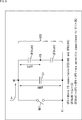
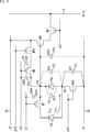
- FIG. 3 is a diagram illustrating an equivalent circuit of a pixel.
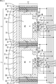
- FIG. 3 is a diagram illustrating a cross-sectional structure of a pixel. It is a figure showing the modification of the section structure of a pixel.
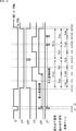
- 4 is a driving timing chart of a pixel.
- FIG. 3 is a diagram illustrating a specific numerical example of electric charge stored in a pixel.
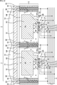
- 3A and 3B are a plan view and a sectional view of a first reset transistor.
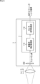
- FIG. 3 is a block diagram of a solid-state imaging device focusing on a signal processing circuit.
- FIG. 3 is a diagram illustrating an equivalent circuit of a pixel.
- FIG. 3 is a diagram illustrating a cross-sectional structure of a pixel. It is a figure showing the modification of the section structure of a pixel.
- 4 is a driving timing
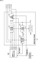
- FIG. 4 is a block diagram illustrating a detailed configuration example of a dark current correction processing unit.
- FIG. 9 is a diagram illustrating a dark current improvement effect by a dark current correction processing unit.
- FIG. 13 is a diagram illustrating an equivalent circuit of a pixel according to the second embodiment.
- FIG. 13 is a diagram illustrating a cross-sectional structure of a pixel according to a second embodiment. 9 is a driving timing chart of a pixel according to the second embodiment.
- FIG. 14 is a diagram illustrating a cross-sectional structure of a pixel according to a third embodiment.
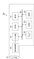
- FIG. 21 is a block diagram illustrating a configuration example of an imaging device as an electronic device to which the present technology is applied.
- FIG. 4 is a diagram illustrating an example of use of an image sensor. It is a block diagram showing an example of a schematic structure of a vehicle control system. It is explanatory drawing which shows an example of the installation position of a vehicle exterior information detection part and an imaging part.
- FIG. 1 shows a schematic configuration of a solid-state imaging device to which the present technology is applied.
- the solid-state imaging device 1 of FIG. 1 includes a pixel array unit 3 in which pixels 2 are arranged in a two-dimensional array and a peripheral circuit unit around the pixel array unit 3 on a semiconductor substrate 12 using, for example, silicon (Si) as a semiconductor. It is composed.
- the peripheral circuit section includes a vertical drive circuit 4, a column signal processing circuit 5, a horizontal drive circuit 6, a signal processing circuit 7, a control circuit 8, and the like.
- the pixel 2 has a photoelectric conversion element such as a photodiode and a plurality of pixel transistors.
- the plurality of pixel transistors are, for example, a transfer transistor, a selection transistor, a reset transistor, an amplification transistor, and the like, and are configured by MOS transistors. Details of the pixel 2 will be described later with reference to FIGS.
- the control circuit 8 receives an input clock and data instructing an operation mode and the like, and outputs data such as internal information of the solid-state imaging device 1. That is, the control circuit 8 generates a clock signal and a control signal, which are references for the operations of the vertical drive circuit 4, the column signal processing circuit 5, the horizontal drive circuit 6, and the like, based on the vertical synchronization signal, the horizontal synchronization signal, and the master clock. I do. Then, the control circuit 8 outputs the generated clock signal and control signal to the vertical drive circuit 4, the column signal processing circuit 5, the horizontal drive circuit 6, and the like.
- the vertical drive circuit 4 is formed of, for example, a shift register, selects a predetermined pixel drive line 10, supplies a pulse for driving the pixel 2 to the selected pixel drive line 10, and drives the pixel 2 in row units. I do. That is, the vertical drive circuit 4 selectively scans each pixel 2 of the pixel array unit 3 sequentially in the vertical direction on a row-by-row basis, and outputs a pixel signal based on signal charges generated in the photoelectric conversion unit of each pixel 2 according to the amount of received light. Is supplied to the column signal processing circuit 5 through the vertical signal line 9.
- the column signal processing circuit 5 is arranged for each column of the pixels 2 and performs signal processing such as noise removal for signals output from the pixels 2 for one row for each pixel column.
- the column signal processing circuit 5 performs signal processing such as CDS (Correlated Double Sampling: correlated double sampling) for removing fixed pattern noise unique to pixels and AD conversion.
- CDS Correlated Double Sampling: correlated double sampling
- the horizontal drive circuit 6 is formed of, for example, a shift register, and sequentially outputs horizontal scanning pulses to sequentially select each of the column signal processing circuits 5 and to output a pixel signal from each of the column signal processing circuits 5 to a horizontal signal line. 11 is output.
- the signal processing circuit 7 performs predetermined signal processing on signals sequentially supplied from each of the column signal processing circuits 5 through the horizontal signal line 11 and outputs the processed signals.
- the signal processing circuit 7 may perform only buffering, or may perform dark current correction, column variation correction, various digital signal processing, and the like.
- the input / output terminal 13 exchanges signals with the outside.
- the solid-state imaging device 1 configured as described above is a CMOS image sensor called a column AD system in which a column signal processing circuit 5 that performs CDS processing and AD conversion processing is arranged for each pixel column.
- the solid-state imaging device 1 is a solid-state imaging device that detects both electrons and holes to realize high dynamic range imaging. Hereinafter, the details of the solid-state imaging device 1 that achieves high dynamic range imaging will be described.
- Pixel circuit and cross-sectional structure The circuit and cross-sectional structure of the pixel 2 that detects both electrons and holes will be described with reference to FIGS.
- FIG. 2 shows an equivalent circuit of the pixel 2
- FIG. 3 shows a cross-sectional structure of the pixel 2.
- a first voltage supply line 31 for applying a first voltage V1 and a second voltage supply line 32 for applying a second voltage V2 include: Connected to pixel 2.
- the first voltage V1 is, for example, a ground voltage (in other words, a GND voltage, 0 V), and the second voltage V2 is, for example, a power supply voltage (in other words, a VDD voltage).
- the first voltage V1 is not limited to 0 V, and may take a negative voltage or a positive voltage lower than the second voltage V2. (In this specification, the first voltage V1 other than the GND voltage may be referred to as VPGB for convenience.)
- the solid-state imaging device 1 includes a variable power supply mechanism that changes the magnitude of the voltage supplied to the pixel 2 with time as a mechanism that supplies the second voltage V2 to the pixel 2 (in other words, a mechanism that supplies power to the pixel 2).
- the variable power supply for example, a high voltage VDD H that a voltage for operating the transistor provided in the voltage and the pixel 2 for resetting the state of the photodiode PD and the floating diffusion FD provided in (1) pixel 2, (2) such as a low voltage VDD L for the stopped state of the operation of the transistor included in the pixel 2 may provide a plurality of kinds of voltages to the pixels 2.
- the size of the low voltage VDD L may be different or may be the same as the first voltage V1.
- the pixel 2 includes a photodiode PD, a first reset transistor MR1, a transfer transistor MT, a conversion gain switching transistor MG, a second reset transistor MR2, an amplification transistor MA, a selection transistor MS, a floating diffusion FD, It includes a first capacitor C1 and a second capacitor C2.
- the transfer transistor MT, the conversion gain switching transistor MG, the second reset transistor MR2, the amplification transistor MA, the selection transistor MS, and the first reset transistor MR1 are configured by MOS transistors. More specifically, the transfer transistor MT, the conversion gain switching transistor MG, the second reset transistor MR2, the amplification transistor MA, and the selection transistor MS are configured by N-type MOS transistors (NMOS transistors), and the first reset transistor MR1 is configured by a P-type MOS transistor (PMOS transistor).
- the node N1 which is the anode of the photodiode PD, is formed of a P-type semiconductor.
- the node N1, which is a P-type semiconductor region, is connected to the first voltage supply line 31 via a first reset transistor MR1, which is a P-type MOS transistor.
- the cathode of the photodiode PD is connected to a floating diffusion FD serving as a charge-voltage converter via a transfer transistor MT.
- the first reset transistor MR1 connects the node N1, which is the anode of the photodiode PD, to the first voltage supply line 31, or disconnects the node N1 from the first voltage supply line 31 to bring the node N1 into a floating state. Take charge of function.
- the first reset transistor MR1 is turned on by the first reset signal ⁇ R1, the node N1 is connected to the first voltage supply line 31, and the node N1 is reset to the first voltage V1.
- the first reset transistor MR1 is turned off by the first reset signal ⁇ R1, the node N1 is in a floating state.
- the floating diffusion FD (in other words, the floating diffusion capacitance FD) is a charge-to-voltage conversion unit, and is also used until a signal converted to a voltage is output outside the pixel via the vertical signal line 9. It also serves as a charge storage section for temporarily holding charges.
- the floating diffusion FD also serves as the drain region (N-type semiconductor diffusion layer region) of the transfer transistor MT. Further, the transfer transistor MT and the floating diffusion FD are formed in a P-type semiconductor region (node N1) serving as an anode of the photodiode PD. Therefore, a PN junction FDJ is formed between the floating diffusion FD and the P-type semiconductor region (node N1) serving as the anode of the photodiode PD.
- the junction capacitance of the PN junction FDJ will be referred to as CJ.
- the floating diffusion FD is connected to the photodiode PD via the transfer transistor MT, and is also connected to the second voltage supply wiring 32 via the conversion gain switching transistor MG and the second reset transistor MR2. Further, the floating diffusion FD is also connected to the gate of the amplification transistor MA.
- the conversion gain switching transistor MG and the second reset transistor MR2 are connected in series, and are disposed between the floating diffusion FD and the second voltage supply wiring 32.
- Conversion gain switching transistor MG switches the conversion gain of floating diffusion FD according to switching signal ⁇ G. Specifically, when the conversion gain switching transistor MG is turned on (on state) by the switching signal ⁇ G, the gate capacitance CG of the conversion gain switching transistor MG is electrically connected to the floating diffusion FD, and The capacity increases. As a result, the voltage signal generated as a result of voltage conversion of a fixed amount of charge in floating diffusion FD is smaller than when conversion gain switching transistor MG is in a non-conductive state, and is in a so-called low conversion gain state.
- the conversion gain switching transistor MG is turned off (off state) by the switching signal ⁇ G
- the gate capacitance CG of the conversion gain switching transistor MG is electrically disconnected from the floating diffusion FD.
- the capacitance of the floating diffusion FD becomes smaller than when the conversion gain switching transistor MG is in the conductive state.
- the voltage signal generated as a result of voltage conversion of a fixed amount of charge in floating diffusion FD is larger than that in the case where conversion gain switching transistor MG is in a conductive state, and is in a so-called high conversion gain state.
- the conversion gain switching transistor MG is simultaneously turned on.
- the amplification transistor MA outputs a pixel signal Vsig corresponding to the potential of the floating diffusion FD to the vertical signal line 9.
- the amplification transistor MA constitutes a source follower circuit with a load MOS (not shown) which is connected to the vertical signal line 9 and functions as a constant current source. Then, the amplification transistor MA converts the pixel signal Vsig indicating the level corresponding to the electric charge held in the floating diffusion FD from the amplification transistor MA into the column signal processing circuit 5 via the selection transistor MS and the vertical signal line 9 (FIG. 1). Output to The load MOS is provided, for example, in the column signal processing circuit 5.
- the selection transistor MS is turned on when the pixel 2 is selected by the selection signal ⁇ S, and outputs the pixel signal Vsig of the pixel 2 to the column signal processing circuit 5 via the vertical signal line 9.
- the transfer signal ⁇ T, the switching signal ⁇ G, the second reset signal ⁇ R2, the first reset signal ⁇ R1, and the selection signal ⁇ S are controlled by a vertical drive circuit 4 which is a drive control unit for controlling the drive of the pixel 2, and the pixel drive wiring 10 (FIG. 1).
- the first capacitor C1 is a capacitor connected between the node N1 serving as the anode of the photodiode PD and the first voltage supply line 31 on the equivalent circuit.
- the first capacitor C1 may be a parasitic capacitance parasitic to a component of the pixel 2 or may be a capacitance intentionally added.
- the first capacitor C1 includes a P-type semiconductor region serving as an anode of a photodiode PD, an electrode disposed inside a trench disposed around each pixel, and a P-type semiconductor region located inside the trench. And an insulating film disposed between the electrode and the electrode.
- the magnitude of the capacitance of the first capacitor C1 may be referred to as CC1.
- a plurality of types of capacitors are connected to the floating diffusion FD.
- the junction capacitance CJ is a capacitance connected between the floating diffusion FD and the node N1 on the equivalent circuit.
- the junction capacitance CJ is a junction capacitance provided between the floating diffusion FD that is an N-type semiconductor diffusion layer region and the node N1 that is a P-type semiconductor region.
- the magnitude of the junction capacitance CJ may be referred to as CCJ.
- the second capacitor C2 is also a capacitor connected between the floating diffusion FD and the node N1 on the equivalent circuit.
- the second capacitor C2 may be a parasitic capacitance parasitic to a component of the pixel 2 or may be a capacitance intentionally added.
- the second capacitor C2 is, for example, a parasitic capacitance generated between the wiring connected to the floating diffusion FD and the node N1, which is a P-type semiconductor region.
- the magnitude of the capacitance of the second capacitor C2 may be referred to as CC2.
- the combined capacitance of the junction capacitance CJ and the second capacitor C2, which is the capacitance connected between the floating diffusion FD and the node N1, may be referred to as the FD capacitance CFDtoN1 for the node N1.
- the size of the FD capacitance CFDtoN1 with respect to the node N1 may be referred to as CCFDtoN1.
- the third capacitor CP3 to the fifth capacitor CP5 are capacitors connected between the floating diffusion FD and the region where the voltage becomes the first voltage V1 in the equivalent circuit.
- the third capacitor CP3 includes a floating diffusion FD, a wiring connected to the floating diffusion FD (a so-called FD wiring), and a first voltage supply line.
- the fourth capacitor CP4 is a parasitic capacitance generated between the floating diffusion FD and a wiring connected to the floating diffusion FD and a wiring for transmitting the transfer signal ⁇ T.
- the magnitude of the capacitance of the third capacitor CP3 to the fifth capacitor CP5 may be referred to as CCP3 to CCP5.
- the parasitic capacitance generated between the floating diffusion FD and the region where the voltage becomes the first voltage V1 may exist in addition to the third to fifth capacitors CP3 to CP5, but is omitted here.
- the third capacitor CP3 to the fifth capacitor CP5 which is a capacitor connected between the floating diffusion FD and the region where the first voltage V1 is provided, and a combined capacitance other than these, are connected to the first voltage V1. May be referred to as the FD capacity CFDtoV1. Further, the magnitude of the FD capacitance CFDtoV1 with respect to the first voltage V1 may be referred to as CCFDtoV1.
- the total capacitance of the floating diffusion FD that is, the combined capacitance of the FD capacitance CFDtoN1 between the floating diffusion FD and the node N1, and the FD capacitance CFDtoV1 between the floating diffusion FD and the region where the first voltage V1 is obtained. It may be called CFD, and the size of the total capacitance CFD of the floating diffusion FD may be called CCFD.
- the gate capacitance CG of the conversion gain switching transistor MG is electrically connected to or disconnected from the floating diffusion FD by the switching signal ⁇ G.
- the magnitude of the gate capacitance CG # of the conversion gain switching transistor MG may be referred to as CCG.
- the pixels 2 are formed in a two-dimensional array.
- An interlayer film 51, a color filter 52, and a microlens 53 are formed in this order on the back surface side of the semiconductor substrate 12, which is the upper side in FIG.
- a material of the interlayer film 51 for example, silicon oxide (SiO2) or the like is used.
- an antireflection film or a fixed charge film made of, for example, silicon nitride (SiN), hafnium oxide (HfO2), or the like may be formed on the back surface side of the semiconductor substrate 12.
- the color filter 52 has, for example, a Bayer array of R (red), G (green), or B (blue).
- the color filter 52 is formed by spin-coating a photosensitive resin containing a pigment such as a pigment or a dye.
- the microlens 53 is formed of, for example, a resin material such as a styrene resin, an acrylic resin, a styrene-acryl copolymer resin, or a siloxane resin.
- a trench isolation 60 penetrating the semiconductor substrate 12 is provided at a boundary between the pixels 2 arranged adjacent to each other.
- the trench isolation 60 includes a trench electrode 61 disposed at the center thereof, and an insulating film 62 disposed outside the trench electrode 61.
- the trench electrode 61 is formed of a metal material such as tungsten (W), aluminum (Al), copper (Cu), or polysilicon.
- the trench electrode 61 is electrically connected to the first voltage supply line 31.
- the insulating film 62 disposed around the trench electrode 61 is formed of an oxide such as silicon oxide (SiO2) or another insulating material.
- the trench isolation 60 including the trench electrode 61 and the insulating film 62 functions as a pixel separation unit that electrically separates adjacent pixels 2.
- Each pixel 2 provided in the pixel array unit 3 includes a photodiode PD.
- the photodiode PD includes an N-type semiconductor region 63 serving as a cathode, and a P-type semiconductor region 64 serving as an anode.
- the photodiode PD provided in the pixel 2 includes a trench isolation 60 penetrating the semiconductor substrate 12 around the photodiode PD. Accordingly, the photodiode PD provided in the pixel 2 is electrically separated from the photodiode PD provided in the adjacent pixel 2 for each pixel.
- the P-type semiconductor region 64 serving as the anode of the photodiode PD is electrically connected to and separated from the first voltage supply line 31 by the first reset transistor MR1.
- the P-type semiconductor region 64 serving as the anode of the photodiode PD is in a floating state when separated from the first voltage supply line 31 by the first reset transistor MR1.
- the N-type semiconductor region 63 serving as the cathode of the photodiode PD is electrically connected to and separated from the floating diffusion FD by the transfer transistor MT.
- the photodiode PD provided in the pixel 2 includes a buried photodiode including a P-type semiconductor region 64 serving as an anode on the side surface, the upper surface, and the lower surface, and an N-type semiconductor region 63 serving as a cathode inside the photodiode PD.
- the P-type semiconductor region 64 is arranged along the inside of the trench isolation 60 (the inside direction of the pixel) arranged at the boundary of each pixel 2.
- the P-type semiconductor region 64 is also arranged along the back surface (upper surface in FIG. 3) of the semiconductor substrate 12 provided in each pixel 2, and further, the pixel 2 in the front surface (lower surface in FIG. 3) of the semiconductor substrate 12.
- the back surface upper surface in FIG. 3
- + of N + or P + represents a region where the concentration of N-type or P-type is high.
- the transfer transistor MT, the conversion gain switching transistor MG, the second reset transistor MR2, the amplification transistor MA, the selection transistor MS, the first reset transistor MR1, the floating diffusion FD, and the like are provided on the lower surface side of the semiconductor substrate 12 in FIG. Is formed. Since the amplification transistor MA and the selection transistor MS cannot be represented by the same cross section, they are represented by circuit symbols. Among these elements, each element except the first reset transistor MR1, which is a PMOS transistor, that is, the transfer transistor MT, the conversion gain switching transistor MG, the second reset transistor MR2, the amplification transistor MA, the selection transistor MS, and the amplification transistor MA The selection transistor MS and the floating diffusion FD are formed in the P-type semiconductor region 64.
- the first reset transistor MR1 which is a PMOS transistor
- the transfer transistor MT When the transfer transistor MT is turned on by the transfer signal ⁇ T, the transfer transistor MT transfers the charges (electrons) accumulated in the N-type semiconductor region 63 to the N-type semiconductor region 65 as the floating diffusion FD.
- the N-type semiconductor region 65 as the floating diffusion FD is connected to the gate of the amplification transistor MA.
- the N-type semiconductor region 66 functions as a drain region of the conversion gain switching transistor MG and a source region of the second reset transistor MR2.
- the N-type semiconductor region 67 functions as a drain region of the second reset transistor MR2, and is connected to the second voltage supply wiring 32 and the drain region of the amplification transistor MA.
- the first reset transistor MR1 is formed in a predetermined region near the surface of the semiconductor substrate 12 and near the trench isolation 60 at the pixel boundary.
- the first reset transistor MR1 is a P-type MOS transistor.
- An N-type well (Well) 69 is formed while being surrounded by the P-type semiconductor region 64.
- the gate electrode of the first reset transistor MR1 is formed on the surface of the N-type well 69 with a gate insulating film interposed therebetween.
- a wiring for transmitting the first reset signal ⁇ R1 is connected to this gate electrode.
- a P-type semiconductor region 68 serving as a drain region of the first reset transistor MR1 is formed in a region of the N-type well 69 where the gate electrode is not formed on the surface.
- the P-type semiconductor region 64 surrounding the N-type well 69 also functions as the source region of the first reset transistor MR1.
- the P-type semiconductor region 68, which is the drain region of the first reset transistor MR1, is connected to the first voltage supply line 31 together with the trench electrode 61.
- the first capacitor C1 is constituted by the trench isolation 60 and the P-type semiconductor region 64 serving as the anode of the photodiode PD.
- the trench electrode 61 connected to the first voltage supply line 31 is one electrode
- the P-type semiconductor region 64 serving as the anode of the photodiode PD is the other electrode.
- the arranged insulating film 62 forms the first capacitor C1.
- the second capacitor C2 is a capacitance generated between the floating diffusion FD and a wiring connected to the floating diffusion FD (so-called FD wiring), and the P-type semiconductor region 64 serving as an anode of the photodiode PD.
- the second capacitor C2 may be a parasitic capacitance parasitic to a component of the pixel 2, or may be a capacitance intentionally added.
- the second capacitor C2 may be a parasitic capacitance generated between a wiring (so-called FD wiring) connected to the floating diffusion FD and a P-type semiconductor region 64 serving as an anode of the photodiode PD.
- the capacitance intentionally added to the P-type semiconductor region 64 can be obtained.
- the capacitance may be intentionally added between the P-type semiconductor region 64 using a wiring different from the FD wiring, or the FD wiring may be formed using an insulating material or a dielectric material different from the interlayer film. The capacitance may be intentionally added to the P-type semiconductor region 64.
- the third capacitor CP3 is a parasitic capacitance generated between the floating diffusion FD and a wiring connected to the floating diffusion FD (so-called FD wiring) and the first voltage supply line 31.
- the fourth capacitor CP4 is a parasitic capacitance generated between the floating diffusion FD and the wiring connected to the floating diffusion FD, and the wiring transmitting the transfer signal ⁇ T.
- the fifth capacitor CP5 is a parasitic capacitance generated between the floating diffusion FD and a wiring connected to the floating diffusion FD, and a wiring transmitting the switching signal ⁇ G.
- the junction capacitance CJ is a junction capacitance formed at a PN junction between the floating diffusion FD, which is an N-type semiconductor diffusion layer region, and the P-type semiconductor region 64, which is the anode of the photodiode PD.
- the gate capacitance CG is the gate capacitance of the conversion gain switching transistor MG.
- the pixel 2 illustrated in FIG. 4 includes, among the pixel transistors included in the pixel 2, NMOS transistors other than the transfer transistor MT (that is, the conversion gain switching transistor MG, the second reset transistor MR2, the amplification transistor MA, and the selection transistor MS).
- the pixel 2 shown in FIG. 3 differs from the pixel 2 shown in FIG. 3 in that it is formed in a second P-type semiconductor region 64b which is electrically separated from the P-type semiconductor region 64.
- the pixel 2 includes a second P-type semiconductor region 64 b different from the P-type semiconductor region 64 on the front surface side (the lower side in FIG. 4) of the semiconductor substrate 12. Further, a second N-type semiconductor region 63b is provided between the P-type semiconductor region 64 and the second P-type semiconductor region 64b. The second N-type semiconductor region 63b is arranged so as to surround the second P-type semiconductor region 64b, thereby electrically separating the P-type semiconductor region 64 from the second P-type semiconductor region 64b. A so-called well-in-well structure is realized. Then, the second P-type semiconductor region 64b is connected to the first voltage supply line 31 via the P-type diffusion layer region 71 formed in the second P-type semiconductor region 64b.
- the drain region of the transfer transistor MT is formed in the P-type semiconductor region 64
- the source region of the conversion gain switching transistor MG is formed in the second P-type semiconductor region 64b
- the drain region of the transfer transistor MT is formed.
- the region and the source region of conversion gain switching transistor MG are electrically connected by wiring.
- the voltage of the P-type semiconductor region 64 in which the pixel transistor is formed may be affected by the amount of holes generated as a result of photoelectric conversion.
- the voltage of the second P-type semiconductor region 64b in which the pixel transistor is formed is constant regardless of the amount of holes generated as a result of photoelectric conversion. This is expected to make the operation of the pixel transistor more stable than the pixel 2 shown in FIG.
- the holes accumulated in the first capacitor C1 are discharged to the first voltage supply line 31 via the first reset transistor MR1, and the first capacitor C1 is reset, and the P-type semiconductor region 64 (FIG. 2) Is fixed at the first voltage V1.
- electrons generated as a result of photoelectric conversion are accumulated in a potential well in the N-type semiconductor region 63 provided in the photodiode PD.
- the stored electrons are transferred to the floating diffusion FD via the transfer transistor MT, where a signal resulting from the charge-voltage conversion is read. .
- the electrons transferred to the floating diffusion FD and the electrons remaining in the potential well in the N-type semiconductor region 63, if any, are transferred via the transfer transistor MT, the conversion gain switching transistor MG, and the second reset transistor MR2. Then, the floating diffusion FD and the potential well in the N-type semiconductor region 63 are reset to the second voltage supply wiring 32.
- the above is the outline of the operation of the pixel 2.
- the second voltage V2 to be supplied to the pixel 2 is set to a high voltage VDD H. State of the high voltage VDD H is maintained until time t4.
- both the P-type semiconductor region 64 and the N-type semiconductor region 63 provided in the photodiode PD and the floating diffusion FD are reset.
- the first reset signal ⁇ R1 is set to Low
- the first reset transistor MR1 is turned on
- the potential of the P-type semiconductor region 64 of the photodiode PD becomes the first level. Reset to voltage V1.
- the transfer signal ⁇ T is set to High and the transfer transistor MT is turned on and the conversion gain switching transistor MG and the second reset transistor MR2 are also turned on, the N-type semiconductor region 63 of the photodiode PD and the floating diffusion FD is reset to the second voltage V2 which is a high voltage VDD H.
- the charge accumulation time (exposure time) in which signal charges are accumulated in accordance with incident light is from time t3 when the reset operation of the P-type semiconductor region 64 and the N-type semiconductor region 63 ends.
- the first reset transistor MR1 is turned off. Thereafter, the holes generated as a result of the photoelectric conversion in the photodiode PD are stored in the first capacitor C1. As the holes are accumulated in the first capacitor C1, the potential of the P-type semiconductor region 64 (node N1 in FIG. 2), which is one electrode of the first capacitor C1, rises from the potential immediately after reset.
- the second voltage V2 is changed from the high voltage VDD H to the low voltage VDD L.
- the second voltage V2 is, from the low voltage VDD L, again, is changed to the high voltage VDD H.
- the period from time t12 to time t13 is a period in which the hole accumulation signal Exp Low 4 is read in the low conversion gain state.
- the selection signal ⁇ S is changed to High
- the selection transistor MS is turned on
- the second reset signal ⁇ R2 is changed to Low
- the second reset transistor MR2 is turned off.
- the floating diffusion FD is separated from the second voltage supply wiring 32.
- the potential of the P-type semiconductor region 64 (node N1 in FIG. 2) that has increased due to the accumulation of holes passes through the FD capacitance CFDtoN1 (combined capacitance of the junction capacitance CJ and the second capacitor C2) with respect to the node N1. And appear in the floating diffusion FD.
- the switching signal ⁇ G is High until the next time t13, and the conversion gain switching transistor MG is in the conductive state. Therefore, the hole accumulation signal Exp Low 4 in the low conversion gain state is output from the floating diffusion FD to the amplification transistor The signal is output to the column signal processing circuit 5 through the MA, the selection transistor MS, and the vertical signal line 9.
- the period from the next time t13 to time t14 is a period in which the hole accumulation signal Exp High 3 is read in the high conversion gain state.
- the switching signal ⁇ G is changed to Low, and the gate capacitance CG of the conversion gain switching transistor MG is disconnected from the floating diffusion FD, so that the floating diffusion FD switches to the high conversion gain state.
- the hole accumulation signal Exp High 3 in the high conversion gain state is output from the floating diffusion FD to the column signal processing circuit 5 through the amplification transistor MA, the selection transistor MS, and the vertical signal line 9.
- the period from time t14 to time t15 is a period in which the hole reference signal Ref High 3 is read in the high conversion gain state.
- the first reset signal ⁇ R1 is changed to Low, and the first reset transistor MR1 is turned on.
- the holes stored in the first capacitor C1 are discharged to the first voltage supply line 31, and the potential of the P-type semiconductor region 64 (node N1 in FIG. 2) is reset to the first voltage V1.
- the potential of the node N1 after the reset appears in the floating diffusion FD via the FD capacitance CFDtoN1 (combined capacitance of the junction capacitance CJ and the second capacitor C2) with respect to the node N1.
- the switching signal ⁇ G is Low, and the conversion gain switching transistor MG is in a non-conductive state, so that the reference signal Ref High 3 of the hole in the high conversion gain state is obtained from the floating diffusion FD.
- the signal is output to the column signal processing circuit 5 through the amplification transistor MA, the selection transistor MS, and the vertical signal line 9.
- a period from the next time t15 to a time t16 is a period in which the hole reference signal Ref Low 4 is read in the low conversion gain state.
- the switching signal ⁇ G is changed to High, and the conversion gain switching transistor MG transits to the conductive state.
- the gate capacitance CG of the conversion gain switching transistor MG is added to the floating diffusion FD, and the floating diffusion FD switches to the low conversion gain state.
- the hole reference signal Ref Low 4 in the low conversion gain state is output from the floating diffusion FD to the column signal processing circuit 5 through the amplification transistor MA, the selection transistor MS, and the vertical signal line 9.
- the second reset signal ⁇ R2 is controlled to be High, and the second reset transistor MR2 is turned on. State. As a result, the floating diffusion FD is reset once.
- the period from the next time t17 to time t23 is a period for reading out the electrons accumulated in the photodiode PD.
- the period from the first time t17 to the time t18 is a period during which the reference signal Ref Low 2 of the electron in the low conversion gain state is read.
- the switching signal ⁇ G is continuously High from time t15 and the conversion gain switching transistor MG is in the conductive state
- the electron reference signal Ref Low 2 in the low conversion gain state is output from the floating diffusion FD to the amplification transistor MA,
- the signal is output to the column signal processing circuit 5 through the selection transistor MS and the vertical signal line 9.
- a period from the next time t18 to a time t19 is a period in which the electronic reference signal Ref High 1 in the high conversion gain state is read.
- the switching signal ⁇ G is changed to Low, and the gate capacitance CG of the conversion gain switching transistor MG is disconnected from the floating diffusion FD, so that the floating diffusion FD switches to the high conversion gain state.
- the electron reference signal Ref High 1 in the high conversion gain state is output from the floating diffusion FD to the column signal processing circuit 5 through the amplification transistor MA, the selection transistor MS, and the vertical signal line 9.
- the period from the next time t19 to time t20 is a transfer period in which the electrons accumulated in the photodiode PD are transferred to the floating diffusion FD in the high conversion gain state.
- the transfer signal ⁇ T is changed to High, and the transfer transistor MT is turned on.
- the switching signal ⁇ G is continuously Low from time t18 and the conversion gain switching transistor MG is in a non-conductive state, so that the floating diffusion FD is in a high conversion gain state. Thereby, the electrons accumulated in the photodiode PD are transferred to the floating diffusion FD in the high conversion gain state.
- the period from the time t20 to the time t21 is a period for reading out the electron accumulation signal Exp High 1 in the high conversion gain state.
- the potential of the floating diffusion FD changes in accordance with the amount of charge of the electrons transferred from the photodiode PD, and the accumulation signal Exp High 1 of the electrons in the high conversion gain state becomes the floating diffusion.
- the signal is output from the FD to the column signal processing circuit 5 through the amplification transistor MA, the selection transistor MS, and the vertical signal line 9.
- the period from the next time t21 to time t22 is a period in which the floating diffusion FD is switched from the high conversion gain state to the low conversion gain state. Also, in case the electrons that could not be transferred from the photodiode PD to the floating diffusion FD in the high conversion gain state remain in the photodiode PD, the electrons remaining in the photodiode PD are added to the floating diffusion FD. It is also a period during which the transfer operation for performing the transfer is performed in parallel.
- the switching signal ⁇ G is changed to High, and the conversion gain switching transistor MG transits to the conductive state.
- the floating diffusion FD is switched to the low conversion gain state by adding the gate capacitance CG of the conversion gain switching transistor MG while holding the electrons transferred from the photodiode PD at the time t19.
- the transfer signal ⁇ T is changed to High, and the transfer transistor MT is turned on. Accordingly, if electrons that cannot be transferred from the photodiode PD to the floating diffusion FD in the high conversion gain state remain in the photodiode PD during the period from the time t19 to the time t20, the remaining electrons are removed. Is transferred from the photodiode PD to the floating diffusion FD in the low conversion gain state.
- a period from the next time t22 to a time t23 is a period for reading out the electron accumulation signal Exp Low 2 in the low conversion gain state.
- the potential of the floating diffusion FD changes in accordance with the amount of charge of the electrons transferred from the photodiode PD, and the accumulation signal Exp Low 2 of the electrons in the low conversion gain state becomes the floating diffusion.
- the signal is output from the FD to the column signal processing circuit 5 through the amplification transistor MA, the selection transistor MS, and the vertical signal line 9.
- the selection signal ⁇ S is changed to Low, the selection transistor MS is turned off, the second reset signal ⁇ R2 is changed to High, and the second reset transistor MR2 is turned on. Further, the first reset signal ⁇ R1 is changed to High, and the first reset transistor MR1 is turned off.
- the hole read operation is performed. From t17 to time t23, the operation of reading out electrons is performed.
- the read operation of the hole reference signal Ref is an operation of reading the electron reference signal Ref from time t17 to time t19, and the operation of reading the electron accumulation signal Exp from time t20 to time t23.
- the floating diffusion FD is in the low conversion gain state from time t12 to time t13, and is in the high conversion gain state from time t13 to time t15.
- the low conversion gain state is from time t15 to time t18
- the high conversion gain state is from time t18 to time t21
- the low conversion gain state is from time t21 to time t23.
- the hole accumulation time is a period from time t3 to time t14, and the electron accumulation time is a period from time t3 to time t20 (high conversion gain state) or time t22 (low conversion gain state). is there.
- the pixel 2 is driven as described above to perform a series of operations of accumulating and reading signal charges.
- Pixel signals of high conversion gain and low conversion gain by electrons are Sig1 and Sig2, respectively, and pixel signals of high conversion gain and low conversion gain by holes are Sig3 and Sig4, respectively.
- the solid-state imaging device 1 outputs a signal based on holes and then outputs a signal based on electrons.
- the first reset transistor MR1 is in a conductive state during a period in which a signal is read out by electrons, specifically, during a period from time t17 to time t23, whereby the potential of the P-type semiconductor region 64 becomes the first voltage. Fixed to V1.
- the P-type semiconductor region 64 not only the N-type semiconductor region 63 of the photodiode PD but also a transfer transistor MT are formed.
- the potential of the P-type semiconductor region 64 in which the transfer transistor MT is formed is set to the first voltage V1. Electrons can be transferred in a fixed state.
- Non-Patent Document 1 that is, the drive that first outputs a signal by electrons and then outputs the signal by holes will be described.
- this driving it is necessary to read out a signal by electrons in a state where the holes generated as a result of the photoelectric conversion are not read out but are stored in the first capacitor C1. That is, as in the hole accumulation period, the first reset transistor MR1 is kept in a non-conductive state, and the holes generated as a result of photoelectric conversion are still accumulated in the first capacitor C1.
- the transfer transistor is transferred from the photodiode PD to the floating diffusion FD in a state where the potential of the P-type semiconductor region 64 (node N1 in FIG. 2) becomes a positive voltage higher than the reset voltage (that is, the first voltage V1). It is necessary to transfer and read electrons using MT.
- a sufficient electric field cannot be applied to the channel of the transfer transistor MT, which may adversely affect the transfer of electrons from the photodiode PD to the floating diffusion FD.
- a potential barrier occurs that hinders the transfer of electrons from the photodiode PD to the floating diffusion FD, and electrons that cannot be transferred to the floating diffusion FD remain in the photodiode PD. There is a concern.
- the transfer transistor MT is set in a state where the potential of the P-type semiconductor region 64 in which the transfer transistor MT is formed is fixed to the reset voltage (that is, the first voltage V1). Can be used to transfer electrons.
- a sufficient electric field can be applied to the channel of the transfer transistor MT, and electrons are transferred from the photodiode PD to the floating diffusion FD using the transfer transistor MT. Transfer performance can be improved. This also reduces the concern that electrons that could not be transferred to the floating diffusion FD remain in the photodiode PD. Therefore, according to the driving according to the present technology, the charge generated as a result of the photoelectric conversion can be read well, and a high-quality image can be obtained.
- the second voltage V2 supplied to the pixel 2 becomes high. from the voltage VDD H, it is changed to the low voltage VDD L which is at a lower voltage than.
- the second voltage V2 the effect will be described for setting a lower voltage than the high voltage VDD H.
- the first reset transistor MR1 is turned off, whereby the P-type semiconductor region 64 (the node N1 in FIG. 2), which is one electrode of the first capacitor C1, is brought into a floating state. , And performs a charge accumulation operation. That is, the pixel 2 accumulates the holes generated in the photodiode PD during the accumulation period in the first capacitor C1.
- an N-type semiconductor region to which a different potential is applied is arranged adjacent to the P-type semiconductor region 64 which is one electrode of the first capacitor C1, and a PN junction is formed at the boundary.
- the junction between the N-type semiconductor region 67 and the P-type semiconductor region 64 in FIG. 3, which is the drain region of the second reset transistor MR2, to which the second voltage supply wiring 32 is connected corresponds to the PN junction.
- the solid-state imaging device 1 drives such that the second voltage V2 applied to the pixel 2 by the second voltage supply wiring 32 is changed in accordance with the operation of the pixel 2.
- the second voltage V2 is set to a high voltage VDD H. From the time t4 after the reset operation is completed, until time t11 before starting the read operation, the second voltage V2 is set to a low voltage VDD L. During this time, the pixel 2 is performing the accumulation operation. And, since time t11, the order to transfer and read operation, the second voltage V2 is set to a high voltage VDD H.
- the high voltage VDD H is 3.0 V
- the low voltage VDD L is assumed to be 1.5V, to become half the voltage across the PN junction, also an electric field applied to the portion is depleted, it becomes about half accordingly
- the generated dark current can be effectively reduced.
- the high voltage VDD H which is the second voltage V2 during a read operation and reset operation, a potential variation occurring upon maximum accumulated charge in the first capacitor C1 only, is set higher than the low voltage VDD L Good.
- the second voltage V2 during the accumulation period other than the read operation and the reset operation is the ground GND (0 V) and the maximum amount of holes is accumulated in the first capacitor C1
- the amount of increase in the potential of the P-type semiconductor region 64 is reduced. If it is 1.0V, the high voltage VDD H during the exposure period can be set to 1.0V.
- FIG. 2 and FIG. 6 show how the potential of the P-type semiconductor region 64 and the floating diffusion FD changes when the pixel 2 performs an accumulation operation and the generated holes are accumulated in the first capacitor C1. This will be described with specific numerical values.
- FIG. 6 is a diagram in which elements required for calculating the potentials of the node N1 and the floating diffusion FD are extracted from FIG.
- the FD capacitance CFDtoN1 for the node N1 is a capacitance connected between the floating diffusion FD and the node N1, and specifically, is a combined capacitance of the junction capacitance CJ and the second capacitor C2.
- the FD capacitance CFDtoV1 with respect to the first voltage V1 is a capacitance connected between the floating diffusion FD and a region where the first voltage V1 is obtained.
- the third capacitor CP3 to the fifth capacitor CP5 and the other This is a combined capacitance obtained by combining capacitances for one voltage V1.
- the total capacitance CFD of the floating diffusion FD is a combined capacitance of the FD capacitance CFDtoN1 for the node N1 and the FD capacitance CFDtoV1 for the first voltage V1.
- the magnitude CCFD of the total capacitance CFD of the floating diffusion FD is 2.5 fF, of which the magnitude CCFDtoN1 of the FD capacitance CFDtoN1 with respect to the node N1 is 1.36 fF, of which the magnitude of the junction capacitance CJ of the PN junction of the floating diffusion FD is It is assumed that CCJ is 0.36 fF and the capacitance CC2 of the second capacitor C2 is 1 fF.
- the capacitance CC2 of the second capacitor C2 is preferably 20 to 80% of the total capacitance CFD of the floating diffusion FD.
- the size CCFD of the total capacitance CFD of the floating diffusion FD is set to 2.5 fF
- the size CC2 of the capacitance of the second capacitor C2 is set to 1 fF.
- the magnitude CCG of the gate capacitance CG of the conversion gain switching transistor MG whose connection and disconnection to the floating diffusion FD is controlled by the switching signal ⁇ G is 10 fF
- the magnitude CC1 of the capacitance of the first capacitor C1 is Assume 100fF.
- the photodiode PD can store up to 30,000 [e] of electrons
- the first capacitor C1 can store up to 100,000 [h] of holes
- the floating diffusion FD can store electrons in a high conversion gain state. It is assumed that 10000 [e] can be stored by using the following equation, and that electrons can be stored at least 30000 [e] in the low conversion gain state.
- the total capacitance CFD of the floating diffusion FD is 2.5 fF, and the elementary charge is 1.6 ⁇ 10 -19 C.
- the total capacitance CFD of the floating diffusion FD is 12.5 fF.
- Is 1.6 ⁇ 10 ⁇ 19 /12.5 ⁇ 10 ⁇ 15 13 ⁇ V / e.
- the size CCFD of the total capacitance CFD of the floating diffusion FD is 2.5 fF
- the size CCFDtoN1 of the FD capacitance CFDtoN1 with respect to the node N1 is 1.36 fF.
- the size CCFD of the total capacitance CFD of the floating diffusion FD is 12.5 fF, and the size CCFDtoN1 of the FD capacitance CFDtoN1 with respect to the node N1 is 1.36 fF.
- the floating diffusion FD has a maximum of 640 mV in the high conversion gain state of electrons, a maximum of 390 mV in the low conversion gain state of electrons, a maximum of 870 mV in the high conversion gain state of holes, and a maximum of 870 mV in the low conversion gain state of holes.
- the accumulation operation using holes can accumulate more charges than the accumulation operation using electrons. Further, in the reading operation using holes, the charge conversion gain can be suppressed lower than in the reading operation using electrons.
- the input range of the pixel signal Vsig input from the pixel 2 to the AD conversion circuit becomes too large. there is a possibility.
- the input range of the pixel signal Vsig to the AD conversion circuit is suppressed by suppressing the conversion gain of the holes to be low. Can be entered.
- the pixel 2 in the high-intensity region is photographed.
- the hole readout signal can output a signal having gradation.
- the electron readout signal outputs a signal with a large output range and rich gradation. Can be.
- first reset transistor MR1> By the way, in a solid-state imaging device, if both an NMOS transistor and a PMOS transistor are arranged in a pixel, it is necessary to form a well for each of the transistors, so that the degree of integration of the pixel is reduced. In order to avoid this reduction in the degree of integration, a solid-state imaging device generally uses only one of an NMOS transistor and a PMOS transistor. When the photodiode PD that stores electrons is used, normally, an NMOS transistor is used.
- the NMOS transistor is used for the transfer transistor MT and the amplification transistor MA except for the first reset transistor MR1, while the first reset transistor is used.
- a PMOS transistor is used for MR1.
- FIG. 7 shows a plan view and a cross-sectional view of the first reset transistor MR1 formed in the pixel 2.
- the first reset transistor MR1 is formed on the front surface side of the semiconductor substrate 12 (the lower surface in FIG. 3).
- the plan view of FIG. 7 is a plan view of the front side of the semiconductor substrate 12, and the cross-sectional view of FIG. 7 is a cross-sectional view near the front side of the semiconductor substrate 12.
- AA of FIG. 7 is a plan view of the first reset transistor MR1.
- FIG. 7B is a sectional view taken along the line YY in FIG. 7A
- FIG. 7C is a sectional view taken along the line XX in FIG. 7A
- the first reset transistor MR1 is arranged at one corner of the pixel 2 having a rectangular planar area.
- the first reset transistor MR1 is arranged at the upper right corner of the four corners of the rectangular pixel 2.
- An insulating film 62 and a trench electrode 61 forming the trench isolation 60 are arranged outside the first reset transistor MR1 in the pixel boundary direction.
- the first reset transistor MR1 has a P-type semiconductor region 64 as a source region on one side of the gate electrode MR1_G and a P-type semiconductor region 68 as a drain region on the other side. It has.
- a high-concentration (N +) N-type diffusion layer region 69 ' is provided.
- This high-concentration (N +) N-type diffusion layer region 69 ' is a region for forming an electrical connection for applying a potential to the N-type well (Well) 69 provided in the first reset transistor MR1 which is a PMOS. .
- the impurity concentration at the surface of the P-type semiconductor region 64 is higher than that at the center of the semiconductor substrate 12, as shown in FIG. Therefore, also in FIG. 7A, P + is written to indicate that the P-type semiconductor region 64 as the source region is a high-concentration P-type semiconductor region.
- the P-type semiconductor region 68 as the drain region is also a high-concentration (P +) P-type semiconductor region.
- a P-type semiconductor region 68 serving as a drain region has a trench isolation insulating film 62 on the upper and right side surfaces, a gate electrode MR1_G on the left side surface, and a high-concentration (N +) concentration on the lower side surface.
- N + high-concentration
- the drain region of a general MOS transistor is electrically isolated from the source region and other elements by surrounding three sides with an element isolation region and one side with a gate electrode.
- the first reset transistor MR1 shown in FIG. 7 is different from a general MOS transistor in that an N-type diffusion layer region 69 'for electrically connecting to the N-type well 69 is arranged on the lower side. By doing so, electrical isolation between the P-type semiconductor region 68 as the drain region and the P-type semiconductor region 64 as the source region is achieved without disposing the element isolation region on the lower side.
- the first reset transistor MR1 of the present technology can be generally used. The effect of making the area smaller than that of a typical MOS transistor is obtained.
- the P-type semiconductor region 68 which is the drain region of the first reset transistor MR1 is disposed in the N-type well 69, and the P-type semiconductor region 64 which is the source region. And electrically isolated.
- the first reset transistor MR1 is provided with an N-type well 69 in the P-type semiconductor region 64, and is formed of a PMOS transistor therein.
- the P-type semiconductor region 64 disposed outside the N-type well 69 is used as a source region.
- the first reset transistor MR1 may be arranged at a place other than one corner of the pixel 2 having the rectangular planar area, for example, at a predetermined side of the rectangle.
- the drain region of the second reset transistor MR2 which is an N-type semiconductor region, is disposed adjacent to the P-type semiconductor region 64, which is one electrode of the first capacitor C1. I have. Therefore, a dark current may be generated at the PN junction.
- the solid-state imaging device 1 performs dark current correction processing for correcting dark current in the signal processing circuit 7 at the subsequent stage of the column signal processing circuit 5 that outputs the pixel signals Sig1 to Sig4 after correlated double sampling (CDS) processing. It can be carried out.
- CDS correlated double sampling
- FIG. 8 is a block diagram of the solid-state imaging device 1 focusing on the signal processing circuit 7.
- the solid-state imaging device 1 includes a signal processing circuit 7 at a stage subsequent to the pixel array signal output unit 100.
- the pixel array signal output unit 100 includes the pixel array unit 3, the vertical drive circuit 4, the column signal processing circuit 5, the horizontal drive circuit 6, and the like shown in FIG.
- the pixel signals Sig1 to Sig4 of each pixel 2 after the multiple sampling (CDS) processing are output.
- the signal processing circuit 7 includes a dark current correction processing unit 111 and a camera signal processing unit 112.
- the dark current correction processing unit 111 performs dark current correction processing for correcting dark current. Details of the dark current correction processing unit 111 will be described later.
- the camera signal processing unit 112 performs predetermined signal processing such as white balance correction processing, gain adjustment, and demosaic processing on the pixel signals Sig1 to Sig4 after the dark current correction.
- the camera signal processing unit 112 outputs the pixel signal after the signal processing as a high dynamic range image.
- FIG. 9 is a block diagram showing a detailed configuration example of the dark current correction processing unit 111.
- the dark current correction processing unit 111 includes a signal amount determination unit 121, a correction coefficient determination unit 122, an average processing unit 123, a frame buffer 124, and a correction calculation unit 125.
- the control circuit 8 determines the accumulation time t int of each pixel 2 according to the amount of received light and the like, and supplies it to the pixel array signal output unit 100 and the dark current correction processing unit 111.
- the pixel array signal output unit 100 performs an accumulation operation (imaging operation) based on the accumulation time t int supplied from the control circuit 8, and obtains a pixel signal Sig1 having a high conversion gain due to electrons and a low conversion due to electrons.
- the pixel signal Sig2 of gain, the pixel signal Sig3 of high conversion gain by holes, and the pixel signal Sig4 of low conversion gain by holes are supplied to the dark current correction processing unit 111.
- the pixel array signal output unit 100 detects the element temperature Tc at the time of light reception, and supplies the same to the dark current correction processing unit 111.
- At least the pixel signal Sig1 (a pixel signal having a high conversion gain by electrons) is supplied from the pixel array signal output unit 100 to the signal amount determination unit 121.
- the signal amount determination unit 121 determines whether or not the subject photographed by each pixel 2 is a dark subject. Specifically, the magnitude of the pixel signal Sig1 (pixel signal of high conversion gain by electrons) output from each pixel 2 is smaller than a predetermined threshold value (in other words, a threshold value for determining that the subject is dark). It is determined whether or not.
- a predetermined threshold value in other words, a threshold value for determining that the subject is dark.
- the magnitude of the pixel signal Sig1 (a pixel signal having a high conversion gain by electrons) is smaller than a predetermined threshold, it is determined that the pixel 2 that has output the signal has photographed a dark subject.
- the signal amount determination unit 121 determines that the pixel 2 has photographed a dark subject
- the pixel signal Sig3 (a pixel signal having a high conversion gain due to holes) output from the pixel 2 is generated as a result of photoelectric conversion.
- the signal due to the holes is negligible, and it is determined that most of the pixel signal Sig3 is a dark current.
- the signal amount determination unit 121 determines whether or not the pixel signal Sig3 (pixel signal of high conversion gain due to holes) output from each pixel 2 can be regarded as almost a dark current. The determination result is supplied to the averaging unit 123.
- the correction coefficient determination unit 122 is supplied with a pixel signal Sig3 (a pixel signal having a high conversion gain due to holes) output from each pixel 2, an accumulation time t int when the signal is obtained, and an element temperature Tc. .
- the pixel signals Sig3 (pixel signals of high conversion gain due to holes) input from each pixel 2 to the correction coefficient determination unit 122 do not always have the same accumulation time t int and element temperature Tc. Therefore, the correction coefficient determination unit 122 converts the pixel signal Sig3 (a pixel signal having a high conversion gain due to holes) captured at different accumulation times t int and element temperatures Tc into an accumulation time t int and an element temperature
- a correction coefficient K for correcting the pixel signal Sig3 ′ (pixel signal with a high conversion gain due to holes, in which the element temperature and the accumulation time are corrected) captured by Tc is determined.
- the correction coefficient determination unit 122 multiplies the pixel signal Sig3 (pixel signal of a high conversion gain by holes) of each pixel supplied from the pixel array signal output unit 100 to the correction coefficient determination unit 122 by the correction coefficient K. I do.
- the correction coefficient determining unit 122 supplies the signal obtained as a result of the multiplication process, that is, the pixel signal Sig3 ′ after correcting the element temperature Tc and the accumulation time t int to the averaging unit 123.
- the averaging unit 123 When the signal amount determination unit 121 regards the pixel signal Sig3 (a pixel signal having a high conversion gain by holes) as a dark current, the averaging unit 123 outputs the pixel signal Sig3 ′ ( A pixel signal having a high conversion gain due to holes, in which the element temperature Tc and the accumulation time t int are corrected, is averaged over a plurality of frames.
- the pixel signal Sig3 ′ in one frame includes dark current shot noise.
- the averaging unit 123 removes dark current shot noise by averaging the pixel signal Sig3 ′ over a plurality of frames, and extracts a dark current fixed pattern noise signal Sdrk.
- the averaging unit 123 causes the frame buffer 124 to store the extracted dark current fixed pattern noise signal Sdrk.
- the signal amount determination is performed.
- the average processing unit 123 averages the pixel signal Sig3 ′ over a plurality of frames using a simple moving average, a weighted moving average, an exponential moving average, etc., for a signal of a pixel that the unit 121 considers to be a dark current. Process (in other words, calculate the average value over a plurality of frames).
- the signal obtained as a result of performing this averaging process is the dark current fixed pattern noise signal Sdrk due to holes.
- the averaging unit 123 causes the frame buffer 124 to store the dark current fixed pattern noise signal Sdrk.
- the correction operation unit 125 performs an operation of correcting the dark current of the signal of each pixel 2 supplied from the pixel array signal output unit 100 to the correction operation unit 125. That is, the dark current fixed pattern noise signal Sdrk of the same pixel stored in the frame buffer 124 is subtracted from the pixel signal Sig3 (a pixel signal having a high conversion gain by holes) supplied to the correction operation unit 125.
- the correction operation unit 125 outputs a signal obtained as a result of performing the subtraction processing, that is, a pixel signal Sig3 ′′ after dark current correction (a pixel signal with a high conversion gain due to holes corrected for dark current).
- the dark current correction processing unit 111 when the pixel signal Sig1 (electron high conversion gain pixel signal) is smaller than the predetermined value, the dark current correction processing unit 111 generates a plurality of pixel signals Sig3 (hole high conversion gain pixel signal).
- the dark current fixed pattern noise signal Sdrk (fixed component) is calculated using the frame, and is subtracted from the pixel signal Sig3 to obtain a pixel signal Sig3 ′′ (dark current corrected positive A pixel signal having a high conversion gain due to the holes is generated.
- This dark current correction process is suitable for a pixel signal in a case where a subject is constantly moving like a vehicle-mounted camera and there is always a chance to capture a sufficiently dark subject over the entire imaging surface within a certain period of time.
- the averaging unit 123 of the above-described dark current correction processing unit 111 calculates the dark current fixed pattern noise by averaging over a plurality of frames. However, the averaging unit 123 calculates the dark current fixed pattern noise using a smoothing process such as a median filter. Noise may be calculated.
- FIG. 10 is a diagram illustrating the dark current improvement effect of the dark current correction processing unit 111.
- FIG. 10A shows the S / N ratio of the pixel signals Sig1 to Sig4 of each pixel when the dark current correction processing is not performed
- FIG. 10B shows the pixel ratio of each pixel when the dark current correction processing is performed.
- the S / N ratio of the signals Sig1 to Sig4 is shown.
- the horizontal axis of each of the graphs A and B in FIG. 10 represents the intensity (light reception amount) of light incident on the pixel.
- the horizontal axis of each of the graphs A and B in FIG. 10 indicates a signal to be output from the solid-state imaging device 1 as a result of the imaging operation in the solid-state imaging device 1 from a signal (Sig1, Sig2) obtained by reading electrons to holes. Is expressed in arbitrary units, where the intensity (light receiving amount) of the light for switching to the read signal (Sig3, Sig4) is 1.
- the vertical axis of each graph represents the SN ratio, and the unit is dB.
- AA and B in FIG. 10 are pixel signals Sig3.
- the pixel signal Sig3 described in FIG. 10A is a pixel signal Sig3 having a high conversion gain due to holes without performing dark current correction, whereas the pixel signal Sig3 described in FIG. This is the pixel signal Sig3 ′′ after the correction.
- the value of the horizontal axis is 1 at which the signal to be output from the solid-state imaging device 1 is switched from the signal by electrons (Sig1, Sig2) to the signal by holes (Sig3, Sig4)
- a in FIG. the step of the SN ratio between the pixel signal Sig2 and the pixel signal Sig3 is large.
- B (the signal after the dark current correction processing) in FIG. 10 the step of the SN ratio between the pixel signal Sig2 and the pixel signal Sig3 ′′ in this portion is small. In other words, FIG. This indicates that the S / N ratio has been improved by performing the operation.
- the step of the SN ratio between the pixel signal Sig2 and the pixel signal Sig3 before the dark current correction process is determined by the ratio of the size CC2 of the capacitance of the second capacitor C2 to the size CCFD of the total capacitance CFD of the floating diffusion FD (CC2 / CCFD).
- the ratio of the magnitude CC2 of the capacitance of the second capacitor C2 to the magnitude CCFD of the total capacitance CFD of the floating diffusion FD be set between 0.2 and 0.8. If the capacitance ratio is reduced so as to approach 0, the step of the SN ratio between the pixel signal Sig2 and the pixel signal Sig3 increases. On the other hand, in order to reduce the step of the SN ratio between the pixel signal Sig2 and the pixel signal Sig3 and increase the capacitance ratio so as to approach 1, it is necessary to increase the capacitance of the second capacitor C2. That is, it is necessary that the second capacitor C2 occupies most of the breakdown of the total capacitance CFD of the floating diffusion FD.
- the ratio of the magnitude CC2 of the capacitance of the second capacitor C2 to the magnitude CCFD of the total capacitance CFD of the floating diffusion FD is set between 0.2 and 0.8.
- FIG. 11 shows an equivalent circuit of the pixel 2 according to the second embodiment
- FIG. 12 shows a cross-sectional structure of the pixel 2 according to the second embodiment
- FIG. 13 is a timing chart illustrating driving of the pixel 2 according to the second embodiment.
- the pixel circuit in FIG. 11 corresponds to the pixel circuit in FIG. 2 in the first embodiment.
- the pixel circuit of FIG. 11 is different from the pixel circuit of FIG. 2 in that the PMOS transistor and the NMOS transistor are interchanged. Therefore, the transfer transistor MT, the conversion gain switching transistor MG, the second reset transistor MR2, the amplification transistor MA, and the selection transistor MS are configured by PMOS transistors, and the first reset transistor MR1 is configured by an NMOS transistor.
- the pixel cross-sectional view of FIG. 12 corresponds to the pixel cross-sectional view of FIG. 3 in the first embodiment.
- the pixel sectional view of FIG. 12 is different from the pixel sectional view of FIG. 3 in that the P-type and the N-type of the semiconductor region are switched.
- the drive timing chart of FIG. 13 corresponds to the drive timing chart of FIG. 5 in the first embodiment.
- the drive timing chart of FIG. 13 is different from the drive timing chart of FIG. 5 in that the polarity (High and Low) of each control signal is switched.
- the signal read out first is an electron signal, and then the signal read out from a hole.
- the second embodiment is the same as the first embodiment except for the above-described points, and thus detailed description of FIGS. 11 to 13 is omitted.
- the second embodiment has the same effect as the first embodiment.
- FIG. 14 is a diagram illustrating a cross-sectional structure of a pixel 2 according to a third embodiment of the solid-state imaging device 1 and having a structure in which a pixel separation unit is electrically separated by a PN junction.
- FIG. 14 portions corresponding to those of the first embodiment shown in FIG. 3 are denoted by the same reference numerals, and descriptions of those portions will be omitted as appropriate.
- the trench electrode 61 and the insulating film 62 of the first embodiment shown in FIG. 3 are replaced with N-type semiconductor regions 141 and 142.
- this embodiment is the same as the first embodiment in other points.
- the P-type semiconductor region 64 serving as one electrode of the first capacitor C1 and the anti-conductive type thereof are provided at the boundary between the adjacent pixels 2.
- An N-type semiconductor region 141 is provided.
- the N-type semiconductor region 141 is formed to penetrate the semiconductor substrate 12 similarly to the trench isolation 60.
- An N-type semiconductor region 142 having a higher impurity concentration than the N-type semiconductor region 141 is formed as a contact in a part of the N-type semiconductor region 141 near the interface on the rear surface of the substrate.
- the second voltage V2 is supplied to the N-type semiconductor region 142 serving as a contact portion, and the N-type semiconductor region 141 and the P-type semiconductor region 64 are electrically insulated and separated in a reverse bias state of a PN junction.
- the PN junction capacitance between the N-type semiconductor region 141 and the P-type semiconductor region 64 corresponds to the first capacitor C1.
- the pixel 2 according to each embodiment of the solid-state imaging device 1 stores the first charge (for example, an electron) generated by photoelectrically converting incident light in the photodiode PD, and stores the second charge (for example, a hole) in the photodiode PD. ) Is stored in the first capacitor C1 provided in the pixel separating section.
- the P-type semiconductor region 64 serving as the anode of the photodiode PD is one electrode of the first capacitor C1 that stores the second charge.
- a transfer transistor MT which is an NMOS is also formed in the P-type semiconductor region 64.
- each pixel 2 outputs a pixel signal based on the second charge stored in the first capacitor C1, it outputs a pixel signal based on the first charge stored in the photodiode PD.
- the potential of the P-type semiconductor region 64 where the transfer transistor MT is formed is changed to the ground GND. Can be fixed.
- the first reset transistor MR1 for resetting the P-type semiconductor region 64, which is one electrode of the first capacitor C1 for storing the second charge, is constituted by a PMOS transistor when the second charge is a hole.
- the second charge is constituted by an NMOS transistor.
- the P-type semiconductor region 64 which is one electrode of the first capacitor C1 for storing the second charge, and the first reset transistor MR1 for resetting the first capacitor C1 have the same conductivity type.
- the P-type semiconductor region 64 which is one electrode of the first capacitor C1 can also serve as the source region of the first reset transistor MR1.
- the area of the source region of the first reset transistor MR1 can be omitted, and the area of the first reset transistor MR1 can be reduced.
- the signal processing circuit 7 provided in the solid-state imaging device 1 determines whether the subject imaged by each pixel 2 is dark based on the readout signal of the first charge from each pixel 2. For the pixel 2 for which it is determined that the imaged subject is dark, the signal processing circuit 7 determines that the readout signal of the second charge from the pixel 2 is not a signal generated as a result of photoelectric conversion but a dark current. . Then, the signal processing circuit 7 performs a correction process for removing the dark current from the read signal of the second charge from the pixel 2 using the signal determined to be the dark current. This brings about an effect that the SN ratio of the pixel signal due to the second charge can be improved.
- the present technology is not limited to application to a solid-state imaging device. That is, the present technology is applied to an image capturing unit (photoelectric conversion unit) such as an imaging device such as a digital still camera or a video camera, a portable terminal device having an imaging function, or a copying machine using a solid-state imaging device for an image reading unit.
- the present invention is applicable to all electronic devices using a solid-state imaging device.
- the solid-state imaging device may be formed as a one-chip, or may be formed as a module having an imaging function in which an imaging unit and a signal processing unit or an optical system are packaged together.
- FIG. 15 is a block diagram illustrating a configuration example of an imaging device as an electronic device to which the present technology is applied.
- An imaging device 200 in FIG. 15 includes an optical unit 201 including a lens group, a solid-state imaging device (imaging device) 202 that employs the configuration of the solid-state imaging device 1 in FIG. Processor) circuit 203.
- the imaging device 200 also includes a frame memory 204, a display unit 205, a recording unit 206, an operation unit 207, and a power supply unit 208.
- the DSP circuit 203, the frame memory 204, the display unit 205, the recording unit 206, the operation unit 207, and the power supply unit 208 are mutually connected via a bus line 209.
- the optical unit 201 captures incident light (image light) from a subject and forms an image on the imaging surface of the solid-state imaging device 202.
- the solid-state imaging device 202 converts the amount of incident light imaged on the imaging surface by the optical unit 201 into an electric signal for each pixel and outputs the electric signal as a pixel signal.
- the solid-state imaging device 1 of FIG. 1 that is, a solid-state imaging device that realizes high dynamic range imaging by detecting both electrons and holes can be used.
- the display unit 205 includes a thin display such as an LCD (Liquid Crystal Display) or an organic EL (Electro Luminescence) display, and displays a moving image or a still image captured by the solid-state imaging device 202.
- the recording unit 206 records a moving image or a still image captured by the solid-state imaging device 202 on a recording medium such as a hard disk or a semiconductor memory.
- the operation unit 207 issues operation commands for various functions of the imaging device 200 under user operation.
- the power supply unit 208 appropriately supplies various power supplies, which are operation power supplies for the DSP circuit 203, the frame memory 204, the display unit 205, the recording unit 206, and the operation unit 207, to these supply targets.
- the solid-state imaging device 1 As described above, by using the solid-state imaging device 1 to which the above-described embodiment is applied as the solid-state imaging device 202, an image with a high dynamic range can be generated. Therefore, even in the imaging device 200 such as a video camera, a digital still camera, and a camera module for a mobile device such as a mobile phone, the quality of a captured image can be improved.
- FIG. 16 is a diagram illustrating a usage example of an image sensor using the solid-state imaging device 1 described above.
- the image sensor using the above-described solid-state imaging device 1 can be used in various cases for sensing light such as visible light, infrared light, ultraviolet light, and X-ray as described below.
- a device that captures images for viewing such as digital cameras and portable devices with camera functions.
- Devices used for traffic such as in-vehicle sensors that capture images of the rear, surroundings, and inside the vehicle, surveillance cameras that monitor running vehicles and roads, and ranging sensors that measure the distance between vehicles, etc.
- Apparatus used for home appliances such as TVs, refrigerators, air conditioners, etc. in order to take images and operate the equipment in accordance with the gestures ⁇ Endoscopes, devices that perform blood vessel imaging by receiving infrared light, etc.
- Equipment used for medical and healthcare purposes such as surveillance cameras for crime prevention and cameras for person authentication
- Skin measuring instruments for photographing skin and scalp Beauty microscope such as -Equipment used for sports, such as action cameras and wearable cameras for sports applications-Used for agriculture, such as cameras for monitoring the condition of fields and crops apparatus
- the technology (the present technology) according to the present disclosure can be applied to various products.
- the technology according to the present disclosure is realized as a device mounted on any type of moving object such as an automobile, an electric vehicle, a hybrid electric vehicle, a motorcycle, a bicycle, a personal mobility, an airplane, a drone, a ship, and a robot. You may.
- FIG. 17 is a block diagram illustrating a schematic configuration example of a vehicle control system that is an example of a mobile object control system to which the technology according to the present disclosure can be applied.
- Vehicle control system 12000 includes a plurality of electronic control units connected via communication network 12001.
- the vehicle control system 12000 includes a drive system control unit 12010, a body system control unit 12020, an outside information detection unit 12030, an inside information detection unit 12040, and an integrated control unit 12050.
- a microcomputer 12051, an audio / video output unit 12052, and a vehicle-mounted network I / F (interface) 12053 are illustrated.
- the drive system control unit 12010 controls the operation of the device related to the drive system of the vehicle according to various programs.
- the driving system control unit 12010 includes a driving force generating device for generating driving force of the vehicle such as an internal combustion engine or a driving motor, a driving force transmission mechanism for transmitting driving force to wheels, and a steering angle of the vehicle. It functions as a control mechanism such as a steering mechanism for adjusting and a braking device for generating a braking force of the vehicle.
- the body control unit 12020 controls the operation of various devices mounted on the vehicle body according to various programs.
- the body control unit 12020 functions as a keyless entry system, a smart key system, a power window device, or a control device for various lamps such as a head lamp, a back lamp, a brake lamp, a blinker, and a fog lamp.
- a radio wave or various switch signals transmitted from a portable device replacing the key may be input to the body control unit 12020.
- the body control unit 12020 receives the input of these radio waves or signals and controls a door lock device, a power window device, a lamp, and the like of the vehicle.
- Out-of-vehicle information detection unit 12030 detects information outside the vehicle equipped with vehicle control system 12000.
- an imaging unit 12031 is connected to the outside-of-vehicle information detection unit 12030.
- the out-of-vehicle information detection unit 12030 causes the imaging unit 12031 to capture an image outside the vehicle, and receives the captured image.
- the out-of-vehicle information detection unit 12030 may perform an object detection process or a distance detection process of a person, a vehicle, an obstacle, a sign, a character on a road surface, or the like based on the received image.
- the imaging unit 12031 is an optical sensor that receives light and outputs an electric signal according to the amount of received light.
- the imaging unit 12031 can output an electric signal as an image or can output the information as distance measurement information.
- the light received by the imaging unit 12031 may be visible light or non-visible light such as infrared light.
- the in-vehicle information detection unit 12040 detects information in the vehicle.
- the in-vehicle information detection unit 12040 is connected to, for example, a driver status detection unit 12041 that detects the status of the driver.
- the driver state detection unit 12041 includes, for example, a camera that captures an image of the driver, and the in-vehicle information detection unit 12040 determines the degree of driver fatigue or concentration based on the detection information input from the driver state detection unit 12041. The calculation may be performed, or it may be determined whether the driver has fallen asleep.
- the microcomputer 12051 calculates a control target value of the driving force generation device, the steering mechanism or the braking device based on the information on the inside and outside of the vehicle acquired by the outside information detection unit 12030 or the inside information detection unit 12040, and the drive system control unit A control command can be output to 12010.
- the microcomputer 12051 implements the functions of ADAS (Advanced Driver Assistance System) including vehicle collision avoidance or impact mitigation, following running based on the following distance, vehicle speed maintaining running, vehicle collision warning, vehicle lane departure warning, and the like. Cooperative control for the purpose.
- ADAS Advanced Driver Assistance System
- the microcomputer 12051 controls the driving force generation device, the steering mechanism, the braking device, and the like based on the information about the surroundings of the vehicle obtained by the outside information detection unit 12030 or the inside information detection unit 12040, so that the driver 120 It is possible to perform cooperative control for automatic driving or the like in which the vehicle travels autonomously without depending on the operation.
- the microcomputer 12051 can output a control command to the body system control unit 12020 based on information on the outside of the vehicle acquired by the outside information detection unit 12030.
- the microcomputer 12051 controls the headlamp in accordance with the position of the preceding vehicle or the oncoming vehicle detected by the outside-of-vehicle information detection unit 12030, and performs cooperative control for the purpose of preventing glare such as switching a high beam to a low beam. It can be carried out.
- the sound image output unit 12052 transmits at least one of a sound signal and an image signal to an output device capable of visually or audibly notifying a passenger of the vehicle or the outside of the vehicle of information.
- an audio speaker 12061, a display unit 12062, and an instrument panel 12063 are illustrated as output devices.
- the display unit 12062 may include, for example, at least one of an on-board display and a head-up display.
- FIG. 18 is a diagram illustrating an example of an installation position of the imaging unit 12031.
- the vehicle 12100 includes imaging units 12101, 12102, 12103, 12104, and 12105 as the imaging unit 12031.
- the imaging units 12101, 12102, 12103, 12104, and 12105 are provided, for example, at positions such as a front nose, a side mirror, a rear bumper, a back door of the vehicle 12100, and an upper portion of a windshield in the vehicle interior.
- the imaging unit 12101 provided on the front nose and the imaging unit 12105 provided above the windshield in the passenger compartment mainly acquire an image in front of the vehicle 12100.
- the imaging units 12102 and 12103 provided in the side mirror mainly acquire images of the side of the vehicle 12100.
- the imaging unit 12104 provided in the rear bumper or the back door mainly acquires an image behind the vehicle 12100.
- the forward images acquired by the imaging units 12101 and 12105 are mainly used for detecting a preceding vehicle, a pedestrian, an obstacle, a traffic light, a traffic sign, a lane, and the like.
- FIG. 18 shows an example of the photographing range of the imaging units 12101 to 12104.
- the imaging range 12111 indicates the imaging range of the imaging unit 12101 provided on the front nose
- the imaging ranges 12112 and 12113 indicate the imaging ranges of the imaging units 12102 and 12103 provided on the side mirrors, respectively
- the imaging range 12114 indicates 13 shows an imaging range of an imaging unit 12104 provided in a rear bumper or a back door.
- a bird's-eye view image of the vehicle 12100 viewed from above is obtained by superimposing image data captured by the imaging units 12101 to 12104.
- At least one of the imaging units 12101 to 12104 may have a function of acquiring distance information.
- at least one of the imaging units 12101 to 12104 may be a stereo camera including a plurality of imaging elements or an imaging element having pixels for detecting a phase difference.
- the microcomputer 12051 calculates a distance to each three-dimensional object in the imaging ranges 12111 to 12114 and a temporal change of the distance (relative speed with respect to the vehicle 12100). , It is possible to extract, as a preceding vehicle, a three-dimensional object that travels at a predetermined speed (for example, 0 km / h or more) in a direction substantially the same as that of the vehicle 12100, which is the closest three-dimensional object on the traveling path of the vehicle 12100. it can.
- a predetermined speed for example, 0 km / h or more
- microcomputer 12051 can set an inter-vehicle distance to be secured before the preceding vehicle and perform automatic brake control (including follow-up stop control), automatic acceleration control (including follow-up start control), and the like. In this way, it is possible to perform cooperative control for automatic driving or the like in which the vehicle travels autonomously without depending on the operation of the driver.
- the microcomputer 12051 converts the three-dimensional object data relating to the three-dimensional object into other three-dimensional objects such as a motorcycle, a normal vehicle, a large vehicle, a pedestrian, a telephone pole, and the like based on the distance information obtained from the imaging units 12101 to 12104. It can be classified and extracted and used for automatic avoidance of obstacles. For example, the microcomputer 12051 distinguishes obstacles around the vehicle 12100 into obstacles that are visible to the driver of the vehicle 12100 and obstacles that are difficult to see. Then, the microcomputer 12051 determines a collision risk indicating a risk of collision with each obstacle, and when the collision risk is equal to or more than the set value and there is a possibility of collision, via the audio speaker 12061 or the display unit 12062. By outputting a warning to the driver through forced driving and avoidance steering via the drive system control unit 12010, driving assistance for collision avoidance can be performed.
- the microcomputer 12051 converts the three-dimensional object data relating to the three-dimensional object into other three-dimensional objects such as a
- At least one of the imaging units 12101 to 12104 may be an infrared camera that detects infrared light.
- the microcomputer 12051 can recognize a pedestrian by determining whether or not a pedestrian exists in the captured images of the imaging units 12101 to 12104. The recognition of such a pedestrian is performed by, for example, extracting a feature point in an image captured by the imaging units 12101 to 12104 as an infrared camera, and performing a pattern matching process on a series of feature points indicating the outline of the object to determine whether the object is a pedestrian.
- the audio image output unit 12052 outputs a rectangular contour for emphasis to the recognized pedestrian.
- the display unit 12062 is controlled so that is superimposed. Further, the sound image output unit 12052 may control the display unit 12062 so as to display an icon or the like indicating a pedestrian at a desired position.
- the technology according to the present disclosure can be applied to the imaging unit 12031 among the configurations described above.
- the solid-state imaging device 1 according to each embodiment described above can be applied as the imaging unit 12031.
- the present technology is not limited to application to a solid-state imaging device that detects the distribution of the amount of incident light of visible light and captures an image as an image, and a solid-state that captures the distribution of the amount of incident infrared light, X-rays, or particles as an image. It can be applied to imaging devices and, in a broad sense, solid-state imaging devices (physical quantity distribution detecting devices) such as fingerprint detection sensors that detect distribution of other physical quantities such as pressure and capacitance and take an image as an image. is there.
- a pixel having a photodiode for photoelectrically converting incident light A drive control unit for controlling the driving of the pixel, The pixel accumulates a first charge generated by photoelectric conversion in the photodiode, accumulates a second charge generated by the photoelectric conversion in a first capacitor provided in a pixel separation unit, The solid-state imaging device, wherein the drive control unit outputs a pixel signal based on the first charge stored in the photodiode after outputting a pixel signal based on the second charge stored in the first capacitor.
- the pixel is A floating diffusion for temporarily holding a charge output outside the pixel,
- the solid-state imaging device according to (1) further including: a second capacitor between the floating diffusion and the semiconductor region.
- the solid-state imaging device according to (2) wherein the second capacitor is set between 0.2 times and 0.8 times the total capacity of the floating diffusion.
- the pixel further includes a transistor that resets the semiconductor region to a fixed potential when outputting a pixel signal based on the second charge accumulated in the semiconductor region, The transistor is configured by a PMOS transistor when the second charge is a hole, and is configured by an NMOS transistor when the second charge is an electron. Any of the above (1) to (3) 3.
- the solid-state imaging device according to item 1.
- the solid-state imaging device wherein the source region of the transistor includes the semiconductor region.
- the drain region of the transistor has a structure in which the drain region is surrounded by a well, a gate electrode, and the pixel separation portion in a plan view, and is insulated and separated from the semiconductor region by the well in a cross-sectional view.
- the solid-state imaging device according to 5).
- the solid-state imaging device according to any one of (1) to (7), wherein the drive control unit sets a supply voltage that is a power supply voltage during a read operation to a different voltage during an accumulation period other than the read operation and the reset operation. .
- the solid-state imaging device wherein the different voltage is 0V.
- the pixel further includes a transistor that resets the semiconductor region to a fixed potential when outputting a pixel signal based on the second charge accumulated in the semiconductor region,
- the solid-state imaging device according to (8) or (9), wherein the drive control unit sets the different voltages to be higher than the fixed potential by an amount of potential change that varies with the number of saturated charges that can be accumulated in the semiconductor region.
- the pixel component due to the second charge is subtracted from the pixel signal due to the second charge by a fixed component calculated using a plurality of frames.
- the correction processing unit calculates the fixed component using a pixel signal based on the second charge of the plurality of frames after correction according to an accumulation time and a temperature.
- the pixel separation unit penetrates a semiconductor substrate and electrically separates adjacent pixels.
- the solid-state imaging device wherein the pixel separation unit includes a fixed potential electrode formed of a metal material or polysilicon.
- One semiconductor region of the PN junction of the photodiode constitutes one electrode of the first capacitor.
- the pixel separation unit is formed of a semiconductor region having a conductivity type opposite to that of the semiconductor region, and to which a predetermined voltage is applied.
- the pixel accumulates a first charge generated by photoelectric conversion in the photodiode, accumulates a second charge generated by the photoelectric conversion in a first capacitor provided in a pixel separation unit,
- the drive control unit outputs a pixel signal based on the second charge stored in the first capacitor, and then outputs a pixel signal based on the first charge stored in the photodiode. Drive method.
- a pixel having a photodiode for photoelectrically converting incident light A drive control unit for controlling the driving of the pixel, The pixel accumulates a first charge generated by photoelectric conversion in the photodiode, accumulates a second charge generated by the photoelectric conversion in a first capacitor provided in a pixel separation unit, The drive control unit outputs a pixel signal based on the second charge stored in the first capacitor, and then outputs a pixel signal based on the first charge stored in the photodiode.
- Electronic equipment for controlling the driving of the pixel, The pixel accumulates a first charge generated by photoelectric conversion in the photodiode, accumulates a second charge generated by the photoelectric conversion in a first capacitor provided in a pixel separation unit, The drive control unit outputs a pixel signal based on the second charge stored in the first capacitor, and then outputs a pixel signal based on the first charge stored in the photodiode.
- 1 solid-state imaging device 2 pixels, 3 pixel array unit, 4 vertical drive circuit, 5 column signal processing circuit, 7 signal processing circuit, PD photodiode, FD floating diffusion, MT transfer transistor, MA amplification transistor, MC switching transistor, MP switching transistor Ground reset transistor, MR1 first reset transistor, MR2 second reset transistor, MS selection transistor, PG pixel ground area, CP1 first capacitor, CP2 second capacitor, 60 trench isolation, 61 trench electrode, 62 insulating film, 63N Semiconductor region, ⁇ 63b ⁇ second N-type semiconductor region, ⁇ 64b ⁇ second P-type semiconductor region, ⁇ 69 ⁇ well, ⁇ 100 ⁇ pixel array signal output unit, ⁇ 111 ⁇ dark current correction processing unit, # 14 N-type semiconductor region, 142 an N-type semiconductor region, 200 an imaging device, 202 solid-state imaging device
Landscapes
- Engineering & Computer Science (AREA)
- Multimedia (AREA)
- Signal Processing (AREA)
- Solid State Image Pick-Up Elements (AREA)
- Transforming Light Signals Into Electric Signals (AREA)
Abstract
本技術は、電子と正孔の両方を検出して、高ダイナミックレンジな撮像を行う固体撮像装置において、高画質の画像を得ることができるようにする固体撮像装置およびその駆動方法、並びに電子機器に関する。 固体撮像装置は、入射光を光電変換するフォトダイオードを有する画素と、画素の駆動を制御する駆動制御部とを備える。画素は、光電変換により発生する第1の電荷をフォトダイオードに蓄積し、光電変換により発生する第2の電荷を画素分離部に設けられた第1キャパシタに蓄積する。駆動制御部は、第1キャパシタに蓄積された第2の電荷による画素信号を出力した後で、フォトダイオードに蓄積された第1の電荷による画素信号を出力させる。本技術は、例えば、電子と正孔の両方を検出して、高ダイナミックレンジな撮像を行う固体撮像装置等に適用できる。
Description
本技術は、固体撮像装置およびその駆動方法、並びに電子機器に関し、特に、電子と正孔の両方を検出して、高ダイナミックレンジな撮像を行う固体撮像装置において、高画質の画像を得るための固体撮像装置およびその駆動方法、並びに電子機器に関する。
電子と正孔の両方を検出して、高ダイナミックレンジな撮像を実現する方法が提案されている(例えば、特許文献1、非特許文献1参照)。この方法では、光電変換による電子は、通常の埋込み型フォトダイオードに蓄積され、正孔は、フォトダイオードの画素接地に蓄積される。入射光により電子と正孔はほぼ同じ量子効率で発生するが、電子は、暗い被写体を高感度で出力し、正孔は、フォトダイオードが電子で飽和してしまうような明るい被写体を低感度で出力する。その結果、電子と正孔による信号を合わせることで、広範囲な明るさの被写体に応答できる高ダイナミックレンジ撮像が可能になる。
F. Lalenne, "A 750 K Photocharge Linear Full Well in a 3.2μm HDR Pixel with Complementary Carrier Collection," Journal of MDPI, Sensors, 18, 305, 2018.
上記文献に開示された方法では、正孔蓄積用容量に蓄積された正孔による信号を読み出す前に、フォトダイオードに蓄積された電子による信号が読み出される。電子による信号を読み出す際、正孔蓄積用容量には光電変換の結果発生した正孔が蓄積されている。これにより、正孔蓄積用容量を構成するP型画素基板の電位は、0Vではなく正の電位となっている。また、上記文献に開示された方法では、電子による信号を読み出す際、P型画素基板が電気的にフローティングとなるよう制御されている。この状態で、電子による信号を読み出すために、転送トランジスタのゲート電極へ正の電圧のパルスを与えると、転送ゲート電極とP型画素基板との間の寄生容量結合を介して、P型画素基板の電位が更に正の方向へ変化してしまう。電子を転送する際にP型画素基板の電位が0Vではなく正の電位になっていると、転送トランジスタのチャネルへ十分な電界を印加できず、このことはフォトダイオードからフローティングディフュージョンへの電子の転送に悪影響を及ぼす。一例として、転送トランジスタのチャネルに、フォトダイオードからフローティングディフュージョンへの電子の転送を阻害する電位障壁が生じてしまい、フローティングディフュージョンへ転送できなかった電子が、フォトダイオードに残留してしまう懸念がある。さらには、フォトダイオードに電子が残留することにより、装置から出力される画像において、残像の発生やSN比の低下といった画質の低下が発生する懸念がある。
本技術は、このような状況に鑑みてなされたものであり、電子と正孔の両方を検出して高ダイナミックレンジな撮像を行う固体撮像装置において、光電変換の結果発生した電荷の読み出しを良好に行うためのものである。
本技術の第1の側面の固体撮像装置は、入射光を光電変換するフォトダイオードを有する画素と、前記画素の駆動を制御する駆動制御部とを備え、前記画素は、光電変換により発生する第1の電荷を前記フォトダイオードに蓄積し、前記光電変換により発生する第2の電荷を画素分離部に設けられた第1キャパシタに蓄積し、前記駆動制御部は、前記第1キャパシタに蓄積された前記第2の電荷による画素信号を出力した後で、前記フォトダイオードに蓄積された前記第1の電荷による画素信号を出力させる。
本技術の第2の側面の固体撮像装置の駆動方法は、入射光を光電変換するフォトダイオードを有する画素と、前記画素の駆動を制御する駆動制御部とを備える固体撮像装置の、前記画素が、光電変換により発生する第1の電荷を前記フォトダイオードに蓄積し、前記光電変換により発生する第2の電荷を画素分離部に設けられた第1キャパシタに蓄積し、前記駆動制御部が、前記第1キャパシタに蓄積された前記第2の電荷による画素信号を出力した後で、前記フォトダイオードに蓄積された前記第1の電荷による画素信号を出力させる。
本技術の第3の側面の電子機器は、入射光を光電変換するフォトダイオードを有する画素と、前記画素の駆動を制御する駆動制御部とを備え、前記画素は、光電変換により発生する第1の電荷を前記フォトダイオードに蓄積し、前記光電変換により発生する第2の電荷を画素分離部に設けられた第1キャパシタに蓄積し、前記駆動制御部は、前記第1キャパシタに蓄積された前記第2の電荷による画素信号を出力した後で、前記フォトダイオードに蓄積された前記第1の電荷による画素信号を出力させる固体撮像装置を備える。
本技術の第1乃至第3の側面においては、光電変換により発生する第1の電荷がフォトダイオードに蓄積され、前記光電変換により発生する第2の電荷が画素分離部に設けられた第1キャパシタに蓄積される。前記第1キャパシタに蓄積された前記第2の電荷による画素信号を出力した後で、前記フォトダイオードに蓄積された前記第1の電荷による画素信号が出力される。
固体撮像装置及び電子機器は、独立した装置であっても良いし、他の装置に組み込まれるモジュールであっても良い。
本技術の第1乃至第3の側面によれば、光電変換の結果発生した電荷の読み出しを良好に行うことができる。
なお、ここに記載された効果は必ずしも限定されるものではなく、本開示中に記載されたいずれかの効果であってもよい。
以下、本技術を実施するための形態(以下、実施の形態という)について説明する。なお、説明は以下の順序で行う。
1.固体撮像装置の概略構成例
2.画素回路と断面構造
3.画素の駆動
4.数値例
5.第1リセットトランジスタMR1の詳細構造
6.暗電流補正処理
7.電子と正孔の極性を反対にした構造
8.画素境界部のその他の構造例
9.まとめ
10.電子機器への適用例
11.移動体への応用例
1.固体撮像装置の概略構成例
2.画素回路と断面構造
3.画素の駆動
4.数値例
5.第1リセットトランジスタMR1の詳細構造
6.暗電流補正処理
7.電子と正孔の極性を反対にした構造
8.画素境界部のその他の構造例
9.まとめ
10.電子機器への適用例
11.移動体への応用例
<1.固体撮像装置の概略構成例>
図1は、本技術を適用した固体撮像装置の概略構成を示している。
図1は、本技術を適用した固体撮像装置の概略構成を示している。
図1の固体撮像装置1は、半導体として例えばシリコン(Si)を用いた半導体基板12に、画素2が2次元アレイ状に配列された画素アレイ部3と、その周辺の周辺回路部とを有して構成される。周辺回路部には、垂直駆動回路4、カラム信号処理回路5、水平駆動回路6、信号処理回路7、制御回路8などが含まれる。
画素2は、フォトダイオード等の光電変換素子と、複数の画素トランジスタを有して成る。複数の画素トランジスタは、例えば、転送トランジスタ、選択トランジスタ、リセットトランジスタ、増幅トランジスタなどであり、MOSトランジスタで構成される。画素2の詳細については、図2及び図3を参照して後述する。
制御回路8は、入力クロックと、動作モードなどを指令するデータを受け取り、また固体撮像装置1の内部情報などのデータを出力する。すなわち、制御回路8は、垂直同期信号、水平同期信号及びマスタクロックに基づいて、垂直駆動回路4、カラム信号処理回路5及び水平駆動回路6などの動作の基準となるクロック信号や制御信号を生成する。そして、制御回路8は、生成したクロック信号や制御信号を、垂直駆動回路4、カラム信号処理回路5及び水平駆動回路6等に出力する。
垂直駆動回路4は、例えばシフトレジスタによって構成され、所定の画素駆動配線10を選択し、選択された画素駆動配線10に画素2を駆動するためのパルスを供給し、行単位で画素2を駆動する。すなわち、垂直駆動回路4は、画素アレイ部3の各画素2を行単位で順次垂直方向に選択走査し、各画素2の光電変換部において受光量に応じて生成された信号電荷に基づく画素信号を、垂直信号線9を通してカラム信号処理回路5に供給させる。
カラム信号処理回路5は、画素2の列ごとに配置されており、1行分の画素2から出力される信号を画素列ごとにノイズ除去などの信号処理を行う。例えば、カラム信号処理回路5は、画素固有の固定パターンノイズを除去するためのCDS(Correlated Double Sampling:相関2重サンプリング)およびAD変換等の信号処理を行う。
水平駆動回路6は、例えばシフトレジスタによって構成され、水平走査パルスを順次出力することによって、カラム信号処理回路5の各々を順番に選択し、カラム信号処理回路5の各々から画素信号を水平信号線11に出力させる。
信号処理回路7は、カラム信号処理回路5の各々から水平信号線11を通して順次に供給される信号に対し、所定の信号処理を行って出力する。信号処理回路7は、例えば、バファリングだけする場合もあるし、暗電流補正、列ばらつき補正、各種デジタル信号処理などが行われる場合もある。入出力端子13は、外部と信号のやりとりをする。
以上のように構成される固体撮像装置1は、CDS処理とAD変換処理を行うカラム信号処理回路5が画素列ごとに配置されたカラムAD方式と呼ばれるCMOSイメージセンサである。
固体撮像装置1は、電子と正孔の両方を検出して、高ダイナミックレンジな撮像を実現する固体撮像装置である。以下では、高ダイナミックレンジな撮像を実現した固体撮像装置1の詳細について説明する。
<2.画素回路と断面構造>
図2および図3を参照して、電子と正孔の両方を検出する画素2の回路と断面構造について説明する。
図2および図3を参照して、電子と正孔の両方を検出する画素2の回路と断面構造について説明する。
図2は、画素2の等価回路を示し、図3は、画素2の断面構造を示している。
図2に示されるように、画素2に対して電圧を与えるための線として、第1電圧V1を与える第1電圧供給線31と、第2電圧V2を与える第2電圧供給配線32とが、画素2へ接続されている。
ここで、第1電圧V1は、例えば接地電圧(言い換えればGND電圧、0V)であり、第2電圧V2は、例えば電源電圧(言い換えればVDD電圧)である。なお、第1電圧V1は、0Vに限らず、負の電圧や、あるいはまた、第2電圧V2よりも低い電圧となる正の電圧も取り得る。(本明細書において、GND電圧以外となる第1電圧V1を、便宜上VPGBと呼ぶことがある)
固体撮像装置1は、画素2に対して第2電圧V2を与える機構(言い換えれば画素2へ電源を供給する機構)として、時間によって画素2へ与える電圧の大きさを変える、可変電源機構を備える。この可変電源機構は、例えば、(1)画素2に備わるフォトダイオードPDやフローティングディフュージョンFDの状態をリセットするための電圧や画素2に備わるトランジスタを動作させるための電圧となる高電圧VDDHと、(2)画素2に備わるトランジスタの動作を停止状態とするための低電圧VDDLとなど、複数種の電圧を画素2に対して与え得る。なお、低電圧VDDLの大きさは、第1電圧V1と同じであってもよいし異なっていてもよい。
図2に示されるように、画素2は、フォトダイオードPD、第1リセットトランジスタMR1、転送トランジスタMT、変換ゲイン切替トランジスタMG、第2リセットトランジスタMR2、増幅トランジスタMA、選択トランジスタMS、フローティングディフュージョンFD、第1キャパシタC1、および、第2キャパシタC2を備える。
転送トランジスタMT、変換ゲイン切替トランジスタMG、第2リセットトランジスタMR2、増幅トランジスタMA、選択トランジスタMS、および、第1リセットトランジスタMR1は、MOSトランジスタで構成される。より具体的には、転送トランジスタMT、変換ゲイン切替トランジスタMG、第2リセットトランジスタMR2、増幅トランジスタMA、および、選択トランジスタMSは、N型のMOSトランジスタ(NMOSトランジスタ)で構成され、第1リセットトランジスタMR1は、P型のMOSトランジスタ(PMOSトランジスタ)で構成される。
フォトダイオードPDのアノードであるノードN1は、P型半導体によって形成されている。P型半導体領域であるノードN1は、P型のMOSトランジスタである第1リセットトランジスタMR1を介して第1電圧供給線31に接続されている。フォトダイオードPDのカソードは転送トランジスタMTを介して、電荷-電圧変換部となるフローティングディフュージョンFDに接続されている。
第1リセットトランジスタMR1は、フォトダイオードPDのアノードであるノードN1を第1電圧供給線31へ接続したり、あるいはまた、ノードN1を第1電圧供給線31から切り離してノードN1をフローティング状態にする機能を担う。第1リセット信号φR1により第1リセットトランジスタMR1が導通状態とされたとき、ノードN1は第1電圧供給線31に接続され、ノードN1は第1電圧V1へとリセットされる。第1リセット信号φR1により第1リセットトランジスタMR1が非導通状態とされたときには、ノードN1はフローティング状態となる。
転送トランジスタMTは、転送信号φTにより導通状態とされたとき、フォトダイオードPDで生成された電荷(電子)を読み出し、フローティングディフュージョンFDに転送する。
フローティングディフュージョンFD(言い換えれば、浮遊拡散容量FD)は、電荷-電圧変換部であり、かつまた、電圧へと変換された信号が垂直信号線9を介して画素外へ出力されるまでの間、一時的に電荷を保持する電荷蓄積部ともなる。フローティングディフュージョンFDは、転送トランジスタMTのドレイン領域(N型半導体拡散層領域)も兼ねている。かつ、転送トランジスタMTとフローティングディフュージョンFDは、フォトダイオードPDのアノードとなるP型半導体領域(ノードN1)内に形成されている。このため、フローティングディフュージョンFDと、フォトダイオードPDのアノードとなるP型半導体領域(ノードN1)の間には、PN接合FDJが形成される。PN接合FDJに備わる接合容量を、CJと呼ぶことにする。フローティングディフュージョンFDは、転送トランジスタMTを介してフォトダイオードPDと接続される他、変換ゲイン切替トランジスタMGおよび第2リセットトランジスタMR2を介して、第2電圧供給配線32に接続されている。さらに、フローティングディフュージョンFDは、増幅トランジスタMAのゲートとも接続されている。
変換ゲイン切替トランジスタMGおよび第2リセットトランジスタMR2は直列に接続され、フローティングディフュージョンFDと第2電圧供給配線32との間に配置されている。変換ゲイン切替トランジスタMGは、切替信号φGに応じて、フローティングディフュージョンFDの変換ゲインを切り替える。具体的には、変換ゲイン切替トランジスタMGが切替信号φGにより導通状態(オン状態)となると、変換ゲイン切替トランジスタMGのゲート容量CGが、フローティングディフュージョンFDへと電気的に接続され、フローティングディフュージョンFDの容量が増加する。これにより、フローティングディフュージョンFDにおいて一定量の電荷を電圧変換した結果生じる電圧信号は、変換ゲイン切替トランジスタMGが非導通状態の場合よりも小さく、いわゆる低変換ゲイン状態となる。一方、変換ゲイン切替トランジスタMGが切替信号φGにより非導通状態(オフ状態)となると、上記変換ゲイン切替トランジスタMGのゲート容量CGが、フローティングディフュージョンFDから電気的に切り離される。その結果、変換ゲイン切替トランジスタMGが導通状態の場合よりもフローティングディフュージョンFDの容量が小さくなる。これにより、フローティングディフュージョンFDにおいて一定量の電荷を電圧変換した結果生じる電圧信号は、変換ゲイン切替トランジスタMGが導通状態の場合よりも大きく、いわゆる高変換ゲイン状態となる。
第2リセットトランジスタMR2は、第2リセット信号φR2により導通状態とされたとき、フローティングディフュージョンFDに保持されている電荷を第2電圧供給配線32へ排出することで、フローティングディフュージョンFDの電位を第2電圧V2へとリセットする。第2リセットトランジスタMR2がリセット動作を行うときは、変換ゲイン切替トランジスタMGも同時に導通状態とされる。
増幅トランジスタMAは、フローティングディフュージョンFDの電位に応じた画素信号Vsigを垂直信号線9へと出力する。増幅トランジスタMAは、垂直信号線9に接続され定電流源として機能する負荷MOS(不図示)とソースフォロワ回路を構成する。そして増幅トランジスタMAは、フローティングディフュージョンFDに保持されている電荷に応じたレベルを示す画素信号Vsigを、増幅トランジスタMAから選択トランジスタMSと垂直信号線9を介してカラム信号処理回路5(図1)へと出力する。負荷MOSは、例えば、カラム信号処理回路5内に設けられている。
選択トランジスタMSは、選択信号φSにより画素2が選択されたとき導通状態とされ、画素2の画素信号Vsigを、垂直信号線9を介してカラム信号処理回路5に出力する。転送信号φT、切替信号φG、第2リセット信号φR2、第1リセット信号φR1、および、選択信号φSは、画素2の駆動を制御する駆動制御部である垂直駆動回路4によって制御され、画素駆動配線10(図1)を介して供給される。
図2において、第1キャパシタC1は、等価回路上、フォトダイオードPDのアノードとなるノードN1と第1電圧供給線31との間に接続された容量である。第1キャパシタC1の具体的な構成は後述するが、画素2の構成要素に寄生した寄生容量であってもよいし、意図的に付加した容量であってもよい。第1キャパシタC1は、一例として、フォトダイオードPDのアノードとなるP型半導体領域と、各画素の周囲に配置されたトレンチの内部に配置された電極と、トレンチの内部であってP型半導体領域と電極との間に配置された絶縁膜と、で構成される容量である。なお、今後、第1キャパシタC1の容量の大きさをCC1と呼ぶことがある。
図2において、フローティングディフュージョンFDには、複数種の容量が接続されている。
接合容量CJは、等価回路上、フローティングディフュージョンFDとノードN1との間に接続された容量である。接合容量CJは、N型半導体拡散層領域であるフローティングディフュージョンFDと、P型半導体領域であるノードN1との間に備わる、接合容量である。なお、今後、接合容量CJの容量の大きさをCCJと呼ぶことがある。
第2キャパシタC2も、等価回路上は、フローティングディフュージョンFDとノードN1との間に接続された容量である。第2キャパシタC2の具体的な構成は後述するが、画素2の構成要素に寄生した寄生容量であってもよいし、意図的に付加した容量であってもよい。第2キャパシタC2は、一例として、フローティングディフュージョンFDに接続された配線と、P型半導体領域であるノードN1との間に生じる、寄生容量である。なお、今後、第2キャパシタC2の容量の大きさをCC2と呼ぶことがある。
フローティングディフュージョンFDとノードN1との間に接続された容量であるところの、接合容量CJと第2キャパシタC2を合わせた合成容量を、ノードN1に対するFD容量CFDtoN1と呼ぶことがある。また、ノードN1に対するFD容量CFDtoN1の大きさを、CCFDtoN1と呼ぶことがある。
第3キャパシタCP3乃至第5キャパシタCP5は、等価回路上は、フローティングディフュージョンFDと、電圧が第1電圧V1となる領域との間に接続された容量である。第3キャパシタCP3乃至第5キャパシタCP5の具体的な構成は後述するが、一例として、第3キャパシタCP3は、フローティングディフュージョンFDおよびこれに接続された配線(いわゆるFD配線)と、第1電圧供給線31との間に生じる寄生容量であり、第4キャパシタCP4は、フローティングディフュージョンFDおよびこれに接続された配線と、転送信号φTを伝送する配線との間に生じる寄生容量であり、第5キャパシタCP5は、フローティングディフュージョンFDおよびこれに接続された配線と、切替信号φGを伝送する配線との間に生じる寄生容量である。なお、今後、第3キャパシタCP3乃至第5キャパシタCP5の容量の大きさをCCP3乃至CCP5と呼ぶことがある。フローティングディフュージョンFDと、電圧が第1電圧V1となる領域との間に生じる寄生容量は、第3キャパシタCP3乃至第5キャパシタCP5以外にも存在し得るが、ここでは省略する。
フローティングディフュージョンFDと第1電圧V1となる領域との間に接続された容量であるところの、第3キャパシタCP3乃至第5キャパシタCP5とこれら以外の寄生容量を合わせた合成容量を、第1電圧V1に対するFD容量CFDtoV1と呼ぶことがある。また、第1電圧V1に対するFD容量CFDtoV1の大きさを、CCFDtoV1と呼ぶことがある。
なお、フローティングディフュージョンFDの総容量、すなわち、フローティングディフュージョンFDとノードN1との間のFD容量CFDtoN1と、フローティングディフュージョンFDと第1電圧V1となる領域との間のFD容量CFDtoV1との、合成容量をCFDと呼ぶことがあり、フローティングディフュージョンFDの総容量CFDの大きさをCCFDと呼ぶことがある。
変換ゲイン切替トランジスタMGのゲート容量CGは、先に述べたように、切替信号φGによって、フローティングディフュージョンFDへ電気的に接続されたり切り離されたりする。なお、今後、変換ゲイン切替トランジスタMGのゲート容量CG の大きさをCCGと呼ぶことがある。
次に、図3を参照して、画素2の断面構造について説明する。
画素アレイ部3では、図3に示されるように、画素2が2次元アレイ状に並んで形成されている。画素2に備わる半導体基板12へは、図3の上側(北側)から光が入射する。そこで、本明細書においては、便宜上、半導体基板12に備わる2つの面のうち、光が入射する側の面(図3の上側(北側)の面)を半導体基板12の裏面と呼び、半導体基板12に備わるもう一方の面(光の入射面に対向する面、図3の下側(南側)の面)を半導体基板12の表面、と呼ぶ。図3において上側となる半導体基板12の裏面側には、層間膜51、カラーフィルタ52、および、マイクロレンズ53が、その順で形成されている。層間膜51の材料には、例えば、酸化シリコン(SiO2)等が用いられる。層間膜51の他に、半導体基板12の裏面側に、例えば、窒化シリコン(SiN)、酸化ハフニウム(HfO2)等による反射防止膜や固定電荷膜等が形成されてもよい。
カラーフィルタ52は、例えば、R(赤色)、G(緑色)、または、B(青色)のベイヤ配列とされている。カラーフィルタ52は、例えば顔料や染料などの色素を含んだ感光性樹脂を回転塗布することによって形成される。マイクロレンズ53は、例えば、スチレン系樹脂、アクリル系樹脂、スチレン-アクリル共重合系樹脂、またはシロキサン系樹脂等の樹脂系材料で形成される。
画素アレイ部3の半導体基板12において、隣接して配置される画素2の境界部分には、半導体基板12を貫通するトレンチアイソレーション60が設けられている。トレンチアイソレーション60は、その中心部に配置されたトレンチ電極61と、トレンチ電極61の外側に配置された絶縁膜62とで構成されている。トレンチ電極61は、タングステン(W)、アルミニウム(Al)、銅(Cu)等の金属材料またはポリシリコンなどで形成される。トレンチ電極61は、第1電圧供給線31に電気的に接続されている。トレンチ電極61の周囲に配置された絶縁膜62は、酸化シリコン(SiO2)等の酸化物あるいはその他の絶縁材料で形成される。トレンチ電極61と絶縁膜62を備えたトレンチアイソレーション60は、隣接する画素2の間を電気的に分離する画素分離部として機能する。
画素アレイ部3に備わる各画素2は、フォトダイオードPDを備える。フォトダイオードPDは、カソードとなるN型半導体領域63、および、アノードとなるP型半導体領域64を備える。
画素2に備わるフォトダイオードPDは、その周囲に半導体基板12を貫通するトレンチアイソレーション60を備える。これにより、画素2に備わるフォトダイオードPDは、隣接する画素2に備わるフォトダイオードPDとの間が、画素毎に電気的に分離されている。フォトダイオードPDのアノードとなるP型半導体領域64は、第1リセットトランジスタMR1によって、第1電圧供給線31と電気的に接続および分離される。フォトダイオードPDのアノードとなるP型半導体領域64は、第1リセットトランジスタMR1によって第1電圧供給線31から切り離されたときには、フローティング状態となる。フォトダイオードPDのカソードとなるN型半導体領域63は、転送トランジスタMTによって、フローティングディフュージョンFDと電気的に接続および分離される。
さらに、画素2に備わるフォトダイオードPDは、その側面と上面と下面にアノードとなるP型半導体領域64を備え、その内側にカソードとなるN型半導体領域63を備えた、埋め込み型のフォトダイオードとなっている。より具体的には、フォトダイオードPDの側面において、P型半導体領域64は、各画素2の境界部に配置されたトレンチアイソレーション60の内側(画素の内側方向)に沿って配置される。また、P型半導体領域64は、各画素2に備わる半導体基板12の裏面(図3の上面)に沿っても配置され、さらに、半導体基板12の表面(図3の下面)のうち、画素2に備わるトランジスタ以外となる領域にも配置される。
なお、図3において、N+またはP+の+は、N型またはP型の濃度が高い領域を表す。
図3において下側となる半導体基板12の表面側には、転送トランジスタMT、変換ゲイン切替トランジスタMG、第2リセットトランジスタMR2、増幅トランジスタMA、選択トランジスタMS、第1リセットトランジスタMR1、フローティングディフュージョンFDなどが形成される。なお、増幅トランジスタMAと選択トランジスタMSは、同一断面で表せないため、回路シンボルで表している。これらの素子のうち、PMOSトランジスタである第1リセットトランジスタMR1を除いた各素子、すなわち、転送トランジスタMT、変換ゲイン切替トランジスタMG、第2リセットトランジスタMR2、増幅トランジスタMA、選択トランジスタMS、増幅トランジスタMA、選択トランジスタMSとフローティングディフュージョンFDは、P型半導体領域64内に形成されている。
転送トランジスタMTは、転送信号φTにより導通状態とされたとき、N型半導体領域63に蓄積されている電荷(電子)を、フローティングディフュージョンFDとしてのN型半導体領域65に転送する。フローティングディフュージョンFDとしてのN型半導体領域65は、増幅トランジスタMAのゲートに接続されている。
N型半導体領域66は、変換ゲイン切替トランジスタMGのドレイン領域および第2リセットトランジスタMR2のソース領域として機能する。N型半導体領域67は、第2リセットトランジスタMR2のドレイン領域として機能し、第2電圧供給配線32と、増幅トランジスタMAのドレイン領域に接続されている。
半導体基板12の表面側で、かつ、画素境界のトレンチアイソレーション60に近い所定の領域には、第1リセットトランジスタMR1が形成されている。第1リセットトランジスタMR1は、P型のMOSトランジスタである。周囲をP型半導体領域64で囲まれた中に、N型ウェル(Well)69が形成される。N型ウェル69の表面にゲート絶縁膜を挟んで第1リセットトランジスタMR1のゲート電極が形成される。このゲート電極には第1リセット信号φR1を伝送する配線が接続される。N型ウェル69の中であって、その表面にゲート電極が形成されていない領域には、第1リセットトランジスタMR1のドレイン領域となるP型半導体領域68が形成される。一方、N型ウェル69を取り囲むP型半導体領域64が、第1リセットトランジスタMR1のソース領域を兼ねる。第1リセットトランジスタMR1のドレイン領域であるP型半導体領域68は、トレンチ電極61とともに第1電圧供給線31に接続されている。
次に、図3を参照して、画素2に備わるキャパシタの構成の例を説明する。
第1キャパシタC1は、トレンチアイソレーション60と、フォトダイオードPDのアノードとなるP型半導体領域64によって構成される。具体的には、第1電圧供給線31に接続されたトレンチ電極61が一方の電極、フォトダイオードPDのアノードとなるP型半導体領域64が他方の電極となり、これら2つの電極とこれらの間に配置された絶縁膜62とで、第1キャパシタC1を構成している。
第2キャパシタC2は、フローティングディフュージョンFDおよびこれに接続された配線(いわゆるFD配線)と、フォトダイオードPDのアノードとなるP型半導体領域64との間に生じる容量である。第2キャパシタC2は、画素2の構成要素に寄生した寄生容量であってもよいし、意図的に付加した容量であってもよい。例えば、第2キャパシタC2は、フローティングディフュージョンFDに接続された配線(いわゆるFD配線)と、フォトダイオードPDのアノードとなるP型半導体領域64との間に生じる寄生容量であってよい。あるいは、フローティングディフュージョンFDに接続された配線(いわゆるFD配線)の一部の幅を、その他の部分の幅よりも大きくすることで、P型半導体領域64との間に意図的に付加した容量であってもよい。あるいは、FD配線と、P型半導体領域64と、FD配線とP型半導体領域64との間に配置された層間膜と、によって形成された寄生容量だけでなく、フローティングディフュージョンFDに接続された配線であってFD配線とは異なる配線を用いてP型半導体領域64との間に意図的に付加した容量であってもよいし、層間膜とは異なる絶縁材料もしくは誘電材料と用いてFD配線とP型半導体領域64との間に意図的に付加した容量であってもよい。
第3キャパシタCP3は、フローティングディフュージョンFDおよびこれに接続された配線(いわゆるFD配線)と、第1電圧供給線31との間に生じる寄生容量である。
第4キャパシタCP4は、フローティングディフュージョンFDおよびこれに接続された配線と、転送信号φTを伝送する配線との間に生じる寄生容量である。
第5キャパシタCP5は、フローティングディフュージョンFDおよびこれに接続された配線と、切替信号φGを伝送する配線との間に生じる寄生容量である。
接合容量CJは、N型半導体拡散層領域であるフローティングディフュージョンFDと、フォトダイオードPDのアノードとなるP型半導体領域64とのPN接合部に形成される、接合容量である。
ゲート容量CGは、変換ゲイン切替トランジスタMGのゲート容量である。
次に、図4を参照して、画素2の断面構造の変形例について説明する。
図4に記載の画素2は、画素2に備わる画素トランジスタのうち、転送トランジスタMT以外のNMOSトランジスタ(すなわち、変換ゲイン切替トランジスタMG、第2リセットトランジスタMR2、増幅トランジスタMA、選択トランジスタMS)が、P型半導体領域64とは電気的に分離された第2のP型半導体領域64b内に形成されている点が、図3に記載の画素2と異なる。
図4において、画素2は、半導体基板12の表面側(図4の下側)に、P型半導体領域64とは異なる第2のP型半導体領域64bを備える。さらに、P型半導体領域64と第2のP型半導体領域64bとの間に、第2のN型半導体領域63bを備える。第2のN型半導体領域63bは、第2のP型半導体領域64bを囲むように配置され、これにより、P型半導体領域64と第2のP型半導体領域64bとを電気的に分離した、いわゆるウェルインウェル(Well in Well)構造を実現している。そして、第2のP型半導体領域64bは、第2のP型半導体領域64b内に形成されたP型拡散層領域71を介して、第1電圧供給線31へと接続されることで、第1電圧V1が与えられている。なお、図4において、転送トランジスタMTのドレイン領域はP型半導体領域64内に形成され、変換ゲイン切替トランジスタMGのソース領域は第2のP型半導体領域64b内に形成され、転送トランジスタMTのドレイン領域と変換ゲイン切替トランジスタMGのソース領域は配線によって電気的に接続されている。
図3に記載の画素2は、画素トランジスタが形成されているP型半導体領域64の電圧が、光電変換の結果発生した正孔の量の影響を受ける可能性がある。一方、図4に記載の画素2は、画素トランジスタが形成されている第2のP型半導体領域64bの電圧が、光電変換の結果発生した正孔の量によらず一定となる。これにより、画素トランジスタの動作が図3に記載の画素2よりも安定になることが期待される。
<3.画素の駆動>
図2と図3を参照して、画素2の動作の概要を説明する。
図2と図3を参照して、画素2の動作の概要を説明する。
画素2に備わるフォトダイオードPDへ光が入射すると、入射光が光電変換されて電子と正孔が発生する。この光電変換を、第1リセットトランジスタMR1が非導通の状態で行うと、光電変換の結果発生した正孔は、第1キャパシタC1に蓄積される。その結果、第1キャパシタC1の一方の電極であるP型半導体領域64(図2におけるノードN1)の電位が上昇し、これに応じて、フローティングディフュージョンFDの電位も上昇する。上昇したフローティングディフュージョンFDの電位が信号として読み出される。読み出し後、第1リセットトランジスタMR1が導通状態にされる。これにより、第1キャパシタC1に蓄積された正孔は、第1リセットトランジスタMR1を介して第1電圧供給線31へと排出され、第1キャパシタC1はリセットされ、P型半導体領域64(図2におけるノードN1)の電位は第1電圧V1に固定される。一方、光電変換の結果発生した電子は、フォトダイオードPDに備わるN型半導体領域63内の電位の井戸に蓄積される。上述の蓄積された正孔が読み出された後に、上述の蓄積された電子は、転送トランジスタMTを介してフローティングディフュージョンFDへと転送され、そこで電荷-電圧変換された結果生じた信号が読み出される。読み出し後、フローティングディフュージョンFDに転送された電子と、もしあればN型半導体領域63内の電位の井戸に残留した電子とが、転送トランジスタMTと変換ゲイン切替トランジスタMGと第2リセットトランジスタMR2を介して第2電圧供給配線32へと排出され、フローティングディフュージョンFDとN型半導体領域63内の電位の井戸はリセットされる。以上が、画素2の動作の概要となる。
次に、図5のタイミングチャートを参照して、画素2の駆動について説明する。
初めに、時刻t1において、画素2へ与える第2電圧V2が、低電圧VDDLから、高電圧VDDHへと設定される。高電圧VDDHの状態は、時刻t4まで維持される。
時刻t1から時刻t4の期間内に、フォトダイオードPDに備わるP型半導体領域64とN型半導体領域63の両方と、フローティングディフュージョンFDとが、リセットされる。具体的には、時刻t2から時刻t3の期間に、第1リセット信号φR1がLowに設定されて第1リセットトランジスタMR1が導通状態とされ、フォトダイオードPDのP型半導体領域64の電位が第1電圧V1へとリセットされる。また、転送信号φTがHighに設定されて転送トランジスタMTが導通状態とされ、変換ゲイン切替トランジスタMGおよび第2リセットトランジスタMR2も導通状態にあるので、フォトダイオードPDのN型半導体領域63とフローティングディフュージョンFDが、高電圧VDDHとなっている第2電圧V2へとリセットされる。
P型半導体領域64とN型半導体領域63のリセット動作が終了する時刻t3以降が、入射光に応じて信号電荷が蓄積される電荷蓄積時間(露光時間)となる。
時刻t3において、第1リセット信号φR1がHighに設定されると、第1リセットトランジスタMR1が非導通状態となる。これ以降、フォトダイオードPDで光電変換の結果発生した正孔は、第1キャパシタC1に蓄積される。正孔が第1キャパシタC1に蓄積されるに従って、第1キャパシタC1の一方の電極であるP型半導体領域64(図2におけるノードN1)の電位は、リセット直後の電位よりも上昇する。
また、時刻t3において、転送信号φTがLowに設定されると、転送トランジスタMTが非導通状態となる。これ以降、フォトダイオードPDで光電変換の結果発生した電子は、N型半導体領域63内の電位の井戸に蓄積される。電子がN型半導体領域63内の電位の井戸に蓄積されるに従って、N型半導体領域63の電位は、リセット直後の電位よりも低下する。
リセット動作より後の時刻t4に、第2電圧V2が、高電圧VDDHから低電圧VDDLへと変更される。
画素2に蓄積された信号電荷を読み出す読み出し動作に入る前の時刻t11において、第2電圧V2が、低電圧VDDLから、再び、高電圧VDDHに変更される。
次の時刻t12から時刻t13の期間は、正孔の蓄積信号ExpLow4を低変換ゲイン状態で読み出す期間である。
すなわち、時刻t12において、選択信号φSがHighに変更され、選択トランジスタMSが導通状態とされるとともに、第2リセット信号φR2がLowに変更され、第2リセットトランジスタMR2が非導通状態とされる。これにより、フローティングディフュージョンFDが第2電圧供給配線32から切り離される。その結果、正孔が蓄積されることにより上昇したP型半導体領域64(図2におけるノードN1)の電位が、ノードN1に対するFD容量CFDtoN1(接合容量CJと第2キャパシタC2の合成容量)を介して、フローティングディフュージョンFDに現れる。
ここで、切替信号φGは次の時刻t13までHighであり、変換ゲイン切替トランジスタMGが導通状態にあるので、低変換ゲイン状態の正孔の蓄積信号ExpLow4が、フローティングディフュージョンFDから、増幅トランジスタMA、選択トランジスタMS、および、垂直信号線9を通して、カラム信号処理回路5に出力される。
次の時刻t13から時刻t14の期間は、正孔の蓄積信号ExpHigh3を高変換ゲイン状態で読み出す期間である。
すなわち、時刻t13において、切替信号φGがLowに変更され、変換ゲイン切替トランジスタMGのゲート容量CGがフローティングディフュージョンFDから切り離されるので、フローティングディフュージョンFDが高変換ゲイン状態に切り替わる。その結果、高変換ゲイン状態の正孔の蓄積信号ExpHigh3が、フローティングディフュージョンFDから、増幅トランジスタMA、選択トランジスタMS、および、垂直信号線9を通して、カラム信号処理回路5に出力される。
次の時刻t14から時刻t15の期間は、正孔の基準信号RefHigh3を高変換ゲイン状態で読み出す期間である。
すなわち、時刻t14において、第1リセット信号φR1がLowに変更され、第1リセットトランジスタMR1が導通状態とされる。これにより、第1キャパシタC1に蓄積されていた正孔が第1電圧供給線31へと排出され、P型半導体領域64(図2におけるノードN1)の電位が、第1電圧V1へとリセットされる。リセット後のノードN1の電位は、ノードN1に対するFD容量CFDtoN1(接合容量CJと第2キャパシタC2の合成容量)を介して、フローティングディフュージョンFDに現れる。
ここで、時刻t15までの間、切替信号φGがLowであり、変換ゲイン切替トランジスタMGが非導通状態にあるので、高変換ゲイン状態の正孔の基準信号RefHigh3が、フローティングディフュージョンFDから、増幅トランジスタMA、選択トランジスタMS、および、垂直信号線9を通して、カラム信号処理回路5に出力される。
次の時刻t15から時刻t16の期間は、正孔の基準信号RefLow4を低変換ゲイン状態で読み出す期間である。
すなわち、時刻t15において、切替信号φGがHighに変更され、変換ゲイン切替トランジスタMGが導通状態に遷移する。これにより、変換ゲイン切替トランジスタMGのゲート容量CGがフローティングディフュージョンFDに追加されるので、フローティングディフュージョンFDが低変換ゲイン状態に切り替わる。その結果、低変換ゲイン状態の正孔の基準信号RefLow4が、フローティングディフュージョンFDから、増幅トランジスタMA、選択トランジスタMS、および、垂直信号線9を通して、カラム信号処理回路5に出力される。
以上の時刻t12から時刻t16までの期間で、正孔に関する信号は全て出力されたので、時刻t16から時刻17の期間において、第2リセット信号φR2がHighに制御され、第2リセットトランジスタMR2が導通状態とされる。これにより、フローティングディフュージョンFDが一旦リセットされる。
次の時刻t17から時刻t23までの期間は、フォトダイオードPDに蓄積された電子を読み出す期間である。
最初の時刻t17から時刻t18の期間は、低変換ゲイン状態の電子の基準信号RefLow2を読み出す期間である。
すなわち、切替信号φGは、時刻t15から引き続きHighであり、変換ゲイン切替トランジスタMGが導通状態にあるので、低変換ゲイン状態の電子の基準信号RefLow2が、フローティングディフュージョンFDから、増幅トランジスタMA、選択トランジスタMS、および、垂直信号線9を通して、カラム信号処理回路5に出力される。
次の時刻t18から時刻t19の期間は、高変換ゲイン状態の電子の基準信号RefHigh1を読み出す期間である。
すなわち、時刻t18において、切替信号φGがLowに変更され、変換ゲイン切替トランジスタMGのゲート容量CGがフローティングディフュージョンFDから切り離されるので、フローティングディフュージョンFDが高変換ゲイン状態に切り替わる。その結果、高変換ゲイン状態の電子の基準信号RefHigh1が、フローティングディフュージョンFDから、増幅トランジスタMA、選択トランジスタMS、および、垂直信号線9を通して、カラム信号処理回路5に出力される。
次の時刻t19から時刻t20の期間は、フォトダイオードPDに蓄積された電子を、高変換ゲイン状態のフローティングディフュージョンFDに転送する転送期間である。
時刻t19から時刻t20の期間では、転送信号φTがHighに変更され、転送トランジスタMTが導通状態とされる。切替信号φGは時刻t18から引き続きLowであり、変換ゲイン切替トランジスタMGが非導通状態にあるので、フローティングディフュージョンFDは高変換ゲイン状態である。これにより、フォトダイオードPDに蓄積された電子が、高変換ゲイン状態のフローティングディフュージョンFDに転送される。
次の時刻t20から時刻t21の期間は、高変換ゲイン状態の電子の蓄積信号ExpHigh1を読み出す期間である。
時刻t20から時刻t21の期間では、フォトダイオードPDから転送されてきた電子の電荷量に応じて、フローティングディフュージョンFDの電位が変化し、高変換ゲイン状態の電子の蓄積信号ExpHigh1が、フローティングディフュージョンFDから、増幅トランジスタMA、選択トランジスタMS、および、垂直信号線9を通して、カラム信号処理回路5に出力される。
次の時刻t21から時刻t22の期間は、フローティングディフュージョンFDを高変換ゲイン状態から低変換ゲイン状態へと切り替える期間である。また、高変換ゲイン状態においてフォトダイオードPDからフローティングディフュージョンFDへ転送しきれなかった電子がフォトダイオードPDに残留している事態に備えて、フォトダイオードPDに残留している電子をフローティングディフュージョンFDへ追加で転送するための転送動作を並行して行う期間でもある。
すなわち、時刻t21において、切替信号φGがHighに変更され、変換ゲイン切替トランジスタMGが導通状態に遷移する。これにより、フローティングディフュージョンFDは、時刻t19においてフォトダイオードPDから転送された電子を保持したまま、変換ゲイン切替トランジスタMGのゲート容量CGが追加されて、低変換ゲイン状態へと切り替わる。これと並行して、転送信号φTがHighに変更され、転送トランジスタMTが導通状態とされる。これにより、時刻t19から時刻t20の期間にフォトダイオードPDから高変換ゲイン状態のフローティングディフュージョンFDへ転送しきれなかった電子がフォトダイオードPDに残留している場合には、その残留していた電子が、フォトダイオードPDから低変換ゲイン状態のフローティングディフュージョンFDに転送される。
次の時刻t22から時刻t23の期間は、低変換ゲイン状態の電子の蓄積信号ExpLow2を読み出す期間である。
時刻t22から時刻t23の期間では、フォトダイオードPDから転送されてきた電子の電荷量に応じて、フローティングディフュージョンFDの電位が変化し、低変換ゲイン状態の電子の蓄積信号ExpLow2が、フローティングディフュージョンFDから、増幅トランジスタMA、選択トランジスタMS、および、垂直信号線9を通して、カラム信号処理回路5に出力される。
以上の時刻t17から時刻t23までの期間で、電子に関する信号は全て出力される。
時刻t23において、選択信号φSがLowに変更され、選択トランジスタMSが非導通状態とされるとともに、第2リセット信号φR2がHighに変更され、第2リセットトランジスタMR2が導通状態とされる。また、第1リセット信号φR1がHighに変更され、第1リセットトランジスタMR1が非導通状態とされる。
時刻t23の後、時刻t24において、画素2に供給される第2電圧V2が、高電圧VDDHから、低電圧VDDLに変更され、画素2のリセット、信号電荷蓄積、および、信号電荷読み出しに係る一連の動作が終了する。
画素2に蓄積された信号電荷の読み出し動作において、出力される信号電荷が正孔であるかまたは電子であるかに着目すると、時刻t12から時刻t16までは、正孔の読み出し動作であり、時刻t17から時刻t23までは、電子の読み出し動作である。
また、読み出す信号が基準信号Refであるかまたは蓄積信号Expであるかに着目すると、時刻t12から時刻t14までは、正孔の蓄積信号Expの読み出し動作であり、時刻t14から時刻t16までは、正孔の基準信号Refの読み出し動作であり、時刻t17から時刻t19までは、電子の基準信号Refの読み出し動作であり、時刻t20から時刻t23までは、電子の蓄積信号Expの読み出し動作である。
さらに、フローティングディフュージョンFDが高変換ゲイン状態であるかまたは低変換ゲイン状態であるかに着目すると、時刻t12から時刻t13までは低変換ゲイン状態であり、時刻t13から時刻t15までは高変換ゲイン状態であり、時刻t15から時刻t18までは低変換ゲイン状態であり、時刻t18から時刻t21までは高変換ゲイン状態であり、時刻t21から時刻t23までは低変換ゲイン状態である。
また、正孔の蓄積時間は、時刻t3から時刻t14までの期間であり、電子の蓄積時間は、時刻t3から時刻t20(高変換ゲイン状態)または時刻t22(低変換ゲイン状態)までの期間である。
画素2は、以上のように駆動して、信号電荷の蓄積および読み出しの一連の動作を行う。
電子による高変換ゲインおよび低変換ゲインの画素信号を、それぞれ、Sig1およびSig2、正孔による高変換ゲインおよび低変換ゲインの画素信号を、それぞれ、Sig3およびSig4とすると、電子による高変換ゲインの画素信号Sig1は、基準信号RefHigh1と蓄積信号ExpHigh1との差分(Sig1=ExpHigh1-RefHigh1)、電子による低変換ゲインの画素信号Sig2は、基準信号RefLow2と蓄積信号ExpLow2との差分(Sig2=ExpLow2-RefLow2)、正孔による高変換ゲインの画素信号Sig3は、基準信号RefHigh3と蓄積信号ExpHigh3との差分(Sig3=ExpHigh3-RefHigh3)、正孔による低変換ゲインの画素信号Sig4は、基準信号RefLow4と蓄積信号ExpLow4との差分(Sig4=ExpLow4-RefLow4)で得られる。
上述した駆動によれば、固体撮像装置1は、正孔による信号を出力した後に、電子による信号を出力する。この場合、電子による信号を読み出す期間、具体的には、時刻t17から時刻t23までの期間、第1リセットトランジスタMR1は導通状態とされ、これにより、P型半導体領域64の電位は、第1電圧V1に固定されている。P型半導体領域64内には、フォトダイオードPDのN型半導体領域63だけでなく、転送トランジスタMTも形成されている。このため、上述した駆動によれば、電子による信号を読み出すために転送トランジスタMTを用いて電子を転送する際、転送トランジスタMTが形成されているP型半導体領域64の電位を第1電圧V1に固定した状態で、電子を転送することができる。
ここで、非特許文献1に開示された駆動、すなわち、まず電子による信号を出力し、次いで正孔による信号を出力する駆動について述べる。この駆動の場合、光電変換の結果発生した正孔を、読み出さずに第1キャパシタC1に蓄積したままの状態で、電子による信号を読み出す必要がある。すなわち、正孔の蓄積期間と同様に、第1リセットトランジスタMR1を非導通としたままの状態で、かつ、光電変換の結果発生した正孔を第1キャパシタC1に蓄積したままの状態で、これにより、P型半導体領域64(図2のノードN1)の電位がリセット時の電圧(すなわち第1電圧V1)よりも高い正の電圧になった状態で、フォトダイオードPDからフローティングディフュージョンFDへ転送トランジスタMTを用いて電子を転送して読み出す必要がある。
この場合、転送トランジスタMTのチャネルへ十分な電界を印加できず、これによりフォトダイオードPDからフローティングディフュージョンFDへの電子の転送に悪影響がおよぶ懸念がある。一例として、転送トランジスタMTのチャネルに、フォトダイオードPDからフローティングディフュージョンFDへの電子の転送を阻害する電位障壁が生じてしまい、フローティングディフュージョンFDへ転送できなかった電子が、フォトダイオードPDに残留してしまう懸念がある。
これに対して、本技術の駆動によれば、転送トランジスタMTが形成されているP型半導体領域64の電位をリセット時の電圧(すなわち第1電圧V1)に固定した状態で、転送トランジスタMTを用いて電子を転送することができる。その結果、非特許文献1に開示された駆動と比較して、転送トランジスタMTのチャネルへ十分な電界を印加することが可能となり、フォトダイオードPDからフローティングディフュージョンFDへ転送トランジスタMTを用いて電子を転送する性能を向上させることができる。またこれにより、フローティングディフュージョンFDへ転送できなかった電子が、フォトダイオードPDに残留してしまう懸念を低減することができる。したがって、本技術の駆動によれば、光電変換の結果発生した電荷の読み出しを良好に行うことができ、高画質の画像を得ることができる。
さらに、上述した本技術の駆動によれば、読み出し動作とリセット動作以外の蓄積期間中、具体的には、時刻t4から時刻t11までの期間、画素2に供給される第2電圧V2が、高電圧VDDHから、それよりも低い電圧である低電圧VDDLに変更される。上記の期間中、第2電圧V2を、高電圧VDDHよりも低い電圧に設定する効果について説明する。
本技術の画素2は、第1リセットトランジスタMR1を非導通状態にして、これにより第1キャパシタC1の一方の電極であるP型半導体領域64(図2におけるノードN1)をフローティング状態にしたうえで、電荷の蓄積動作を行う。すなわち、画素2は、蓄積期間中にフォトダイオードPDで発生した正孔を、第1キャパシタC1に蓄積する。
しかし、第1キャパシタC1の一方の電極であるP型半導体領域64には、これと異なる電位が与えられたN型半導体領域が隣接して配置され、その境界部にPN接合が形成されている。例えば、第2電圧供給配線32が接続されている、第2リセットトランジスタMR2のドレイン領域である図3のN型半導体領域67とP型半導体領域64との接合部が上記PN接合に該当する。このPN接合の空乏層領域において例えば熱励起によって電子-正孔対が生成すると、生成した正孔は第1キャパシタC1に蓄積されてしまう。この現象によって蓄積された正孔は、画素2の暗電流固定パターンノイズとして、画素2の特性を悪化させてしまう可能性がある。
そこで、第2電圧供給配線32が接続されているN型半導体領域67と、第1キャパシタC1の一方の電極であるP型半導体領域64と、の間のPN接合における暗電流の発生を低減するため、固体撮像装置1は、第2電圧供給配線32が画素2へ与える第2電圧V2を、画素2の動作に合わせて変更するように駆動する。
具体的には、フォトダイオードPDとフローティングディフュージョンFDをリセットするために、時刻t1から時刻t4の期間は、第2電圧V2が高電圧VDDHに設定される。リセット動作終了後の時刻t4から、読出し動作開始前の時刻t11までの間、第2電圧V2は低電圧VDDLに設定される。この間、画素2は蓄積動作を実行している。そして、時刻t11以降は、転送および読出し動作を行うため、第2電圧V2は高電圧VDDHに設定される。
蓄積動作を実行している時刻t4から時刻t11までの間、N型半導体領域67に接続している第2電圧供給配線32の第2電圧V2は低電圧VDDLに設定されているため、N型半導体領域67とP型半導体領域64との間のPN接合における暗電流の発生を低減することができる。
例えば、高電圧VDDHは3.0V、低電圧VDDLは1.5Vであるとすると、PN接合にかかる電圧は半分になるため、空乏化している部分にかかる電界も、それに応じて約半分になり、発生する暗電流を効果的に低減することができる。なお、読み出し動作とリセット動作中の第2電圧V2である高電圧VDDHは、第1キャパシタC1に電荷を最大限蓄積した際に生じる電位変化量だけ、低電圧VDDLよりも高く設定すればよい。例えば、読み出し動作とリセット動作以外の蓄積期間中の第2電圧V2が接地GND(0V)で、第1キャパシタC1に正孔を最大限蓄積した結果、P型半導体領域64の電位の上昇量が1.0Vである場合、露光期間中の高電圧VDDHは1.0Vに設定することができる。
<4.数値例>
画素2が蓄積動作を行い、発生した正孔が第1キャパシタC1に蓄積されると、P型半導体領域64とフローティングディフュージョンFDの電位がどのくらい変化するかを、図2と図6を参照して具体的数値で説明する。
画素2が蓄積動作を行い、発生した正孔が第1キャパシタC1に蓄積されると、P型半導体領域64とフローティングディフュージョンFDの電位がどのくらい変化するかを、図2と図6を参照して具体的数値で説明する。
図6は、ノードN1とフローティングディフュージョンFDの電位の算出に必要となる素子を図2の中から抽出した図である。ここで、ノードN1に対するFD容量CFDtoN1は、フローティングディフュージョンFDとノードN1との間に接続された容量であり、具体的には接合容量CJと第2キャパシタC2の合成容量である。第1電圧V1に対するFD容量CFDtoV1は、フローティングディフュージョンFDと第1電圧V1となる領域との間に接続された容量であり、具体的には第3キャパシタCP3乃至第5キャパシタCP5とこれら以外の第1電圧V1に対する容量を合わせた合成容量である。フローティングディフュージョンFDの総容量CFDは、ノードN1に対するFD容量CFDtoN1と第1電圧V1に対するFD容量CFDtoV1の合成容量である。
数値の算出においては、以下の仮定を用いる。フローティングディフュージョンFDの総容量CFDの大きさCCFDが2.5fFであり、このうち、ノードN1に対するFD容量CFDtoN1の大きさCCFDtoN1が1.36fFであり、そのうち、フローティングディフュージョンFDのPN接合の接合容量CJの大きさCCJが0.36fF、第2キャパシタC2の容量の大きさCC2が1fFと仮定する。なお、第2キャパシタC2の容量の大きさCC2は、フローティングディフュージョンFDの総容量CFDの大きさCCFDの2割から8割が好ましい。このためここでは、フローティングディフュージョンFDの総容量CFDの大きさCCFDを2.5fF、第2キャパシタC2の容量の大きさCC2を1fFとしている。さらに、切替信号φGによってフローティングディフュージョンFDへの接続と分離が制御される変換ゲイン切替トランジスタMGのゲート容量CGの大きさCCGが10fFであると仮定し、第1キャパシタC1の容量の大きさCC1が100fFであると仮定する。
また、フォトダイオードPDには電子を最大で30000[e]蓄積でき、第1キャパシタC1には正孔を最大で1000000[h]蓄積でき、フローティングディフュージョンFDには、高変換ゲイン状態において電子を最大で10000[e]蓄積できると仮定し、低変換ゲイン状態において電子を30000[e]以上蓄積できると仮定する。
変換ゲイン切替トランジスタMGのゲート容量CGをフローティングディフュージョンFDから切り離した高変換ゲイン状態において、フローティングディフュージョンFDの総容量CFDは2.5fFであり、電気素量は1.6x10⁻¹⁹Cであるから、電子読み出しにおける高変換ゲイン(電子1個当りの出力電圧)は、1.6x10⁻¹⁹ / 2.5x10-15 = 64μV/eである。変換ゲイン切替トランジスタMGのゲート容量CGをフローティングディフュージョンFDに接続した低変換ゲイン状態において、フローティングディフュージョンFDの総容量CFDは12.5fFであるから、電子読み出しにおける低変換ゲイン(電子1個当りの出力電圧)は、1.6x10-19 / 12.5x10-15 = 13μV/eである。
電子を読み出す場合、フローティングディフュージョンFDには高変換ゲイン状態において最大で10000[e]蓄積できることから、高変換ゲイン状態においてフローティングディフュージョンFDには最大で64x10-6 x 10000 = 640mVの電位変化が現れる。低変換ゲイン状態においてはフォトダイオードPDに蓄積できる最大の電子数30000[e]をフローティングディフュージョンFDに蓄積できることから、低変換ゲイン状態においてフローティングディフュージョンFDには最大で13x10-6 x 30000 = 390mVの電位変化が現れる。
正孔に関しては、第1キャパシタC1に最大で1000000[h]が蓄積できることから、フォトダイオードPDにおいて光電変換の結果正孔が発生すると、ノードN1には最大で1.6x10-19 x 1000000 = 160fCの電荷が与えられる。第1キャパシタC1の大きさが100fFであるから、ノードN1に現れる電位変化は最大で、160x10-15 / 100x10-15 = 1600mVとなる。
正孔を読み出す場合、高変換ゲイン状態においては、フローティングディフュージョンFDの総容量CFDの大きさCCFDは2.5fFであり、ノードN1に対するFD容量CFDtoN1の大きさCCFDtoN1は1.36fFであることから、ノードN1に最大で1600mVの電位変化が現れる場合、フローティングディフュージョンFDには、最大で1600 x 1.36x10-15 / 2.5x10-15 = 870mVの電位変化が現れる。低変換ゲイン状態においては、フローティングディフュージョンFDの総容量CFDの大きさCCFDは12.5fFであり、ノードN1に対するFD容量CFDtoN1の大きさCCFDtoN1は1.36fFであることから、ノードN1に最大で1600mVの電位変化が現れる場合、フローティングディフュージョンFDには、最大で1600 x 1.36x10-15 / 12.5x10-15 = 170mVの電位変化が現れる。正孔1000000[h]で上記の電位変化が現れることから、正孔読み出しにおける高変換ゲインは、870x10-3 / 1000000 = 0.87μV/h、低変換ゲインは、170x10-3 / 1000000 = 0.17μV/hとなる。
以上まとめて、フローティングディフュージョンFDには、電子の高変換ゲイン状態で最大640mV、電子の低変換ゲイン状態で最大390mV、正孔の高変換ゲイン状態で最大870mV、正孔の低変換ゲイン状態で最大170mVの電位変化が現れる。
図2乃至図4の画素構造によれば、正孔を用いた蓄積動作は、電子を用いた蓄積動作よりも、多くの電荷を蓄積することができる。また、正孔を用いた読み出し動作は、電子を用いた読み出し動作よりも、電荷の変換ゲインを低く抑えることができる。画素2に多くの正孔を蓄積した場合、これを単純に電荷-電圧変換すると、画素2からAD変換回路(カラム信号処理回路5)へ入力する画素信号Vsigの入力レンジが大きくなりすぎてしまう可能性がある。図2乃至図4の画素構造によれば、画素2に多くの正孔を蓄積した場合でも、正孔の変換ゲインを低く抑えることで、AD変換回路への画素信号Vsigの入力レンジを抑えて入力することができる。
また、図2乃至図4の画素構造によれば、撮影対象とする被写体の中に、被写体の輝度が低い領域と被写体の輝度が高い領域とが混在する場合、高輝度領域を撮影した画素2において、電子の読み出し信号が飽和して階調性を失っても、正孔の読み出し信号が階調性を備えた信号を出力することができる。一方、低輝度領域を撮影した画素2において、正孔の読み出し信号の出力レンジが小さく階調性に乏しくても、電子の読み出し信号は出力レンジが大きく階調性に富んだ信号を出力することができる。そして、電子の読み出し信号のダークランダムノイズレベル(ノイズフロア)が1.0[e]、正孔の最大蓄積量が1000000[h]であれば、電子および正孔を同一の蓄積時間設定とした条件でも、入射光に対して120dB(=20log10(1000000[h]/1.0[e]))の応答をする高ダイナミックレンジの信号を、現実的なフローティングディフュージョンFDの電圧振幅範囲(言い換えれば、後段のAD変換回路がAD変換しやすい入力レンジ)で得ることができる。
<5.第1リセットトランジスタMR1の詳細構造>
ところで、固体撮像装置において、画素内にNMOSトランジスタとPMOSトランジスタの両方を配置すると、それぞれに対してウェルを形成する必要があるため、画素の集積度が低下してしまう。この集積度の低下を避けるため、固体撮像装置では、一般的に、NMOSトランジスタまたはPMOSトランジスタのどちらか一方のみが用いられる。電子を蓄積するフォトダイオードPDを用いる場合、通常は、NMOSトランジスタが用いられる。
ところで、固体撮像装置において、画素内にNMOSトランジスタとPMOSトランジスタの両方を配置すると、それぞれに対してウェルを形成する必要があるため、画素の集積度が低下してしまう。この集積度の低下を避けるため、固体撮像装置では、一般的に、NMOSトランジスタまたはPMOSトランジスタのどちらか一方のみが用いられる。電子を蓄積するフォトダイオードPDを用いる場合、通常は、NMOSトランジスタが用いられる。
しかしながら、本技術の固体撮像装置1では、図2を参照して説明したように、第1リセットトランジスタMR1を除く、転送トランジスタMTや増幅トランジスタMAなどにはNMOSトランジスタを用いる一方、第1リセットトランジスタMR1にはPMOSトランジスタを用いている。
図7を参照して、第1リセットトランジスタMR1にPMOSトランジスタを用いることの効果を説明する。
図7は、画素2内に形成された第1リセットトランジスタMR1の平面図と断面図を示している。図3を参照して説明したように、第1リセットトランジスタMR1は半導体基板12の表面側(図3の下側の面)に形成されている。このため、図7の平面図は、半導体基板12の表面側の平面図であり、図7の断面図は、半導体基板12の表面側近傍の断面図である。
図7のAは、第1リセットトランジスタMR1の平面図である。
図7のBは図7のAにおけるY-Y線断面図、図7のCは図7のAにおけるX-X線断面図、図7のDは図7のAにおけるY’-Y’線断面図、および、図7のEは図7のAにおけるX’-X’線断面図である。
図7のBのY-Y線断面図は、図3の断面図の第1リセットトランジスタMR1付近と同じである。
図7のAの平面図に示されるように、第1リセットトランジスタMR1は、矩形の平面領域を有する画素2の1つの角部に配置される。図7のAでは、矩形の画素2が備える4つの角部のうち右上の角部に、第1リセットトランジスタMR1が配置されている。第1リセットトランジスタMR1の画素境界方向の外側には、トレンチアイソレーション60を構成する絶縁膜62とトレンチ電極61が配置されている。
図7のAの平面視において、第1リセットトランジスタMR1は、ゲート電極MR1_Gを挟んだ一方の側にソース領域としてのP型半導体領域64、もう一方の側にドレイン領域としてのP型半導体領域68を備えている。P型半導体領域68の隣りには、高濃度(N+)のN型拡散層領域69’が設けられている。この高濃度(N+)のN型拡散層領域69’は、PMOSである第1リセットトランジスタMR1に備わるN型ウェル(Well)69へ、電位を与えるための電気的接続を、形成する領域である。
P型半導体領域64の表面部分の不純物濃度は、図3に示したように、半導体基板12の中心部分よりも高く形成されている。このため、図7のAにおいても、ソース領域としてのP型半導体領域64が高濃度P型半導体領域であることを表すよう、P+と表記してある。ドレイン領域としてのP型半導体領域68も高濃度(P+)のP型半導体領域である。図7のAにおいて、ドレイン領域となるP型半導体領域68は、上側と右側の側面をトレンチアイソレーションの絶縁膜62、左側の側面をゲート電極MR1_G、下側の側面を高濃度(N+)のN型拡散層領域69’によって囲まれることにより、ソース領域としてのP型半導体領域64から電気的に分離されている。
一般的なMOSトランジスタのドレイン領域は、3辺を素子分離領域、1辺をゲート電極で囲まれることにより、ソース領域や他の素子から電気的に分離される。しかし、図7に記載の第1リセットトランジスタMR1は、一般的なMOSトランジスタと異なり、下側の辺にはN型ウェル69への電気的接続をとるためのN型拡散層領域69’を配置することで、下側の辺に素子分離領域を配置することなく、ドレイン領域であるP型半導体領域68とソース領域であるP型半導体領域64との電気的分離を達成している。ドレイン領域であるP型半導体領域68に隣接して配置するアイソレーション領域を、ドレイン領域の上側と右側の2辺のみに削減したレイアウトを用いることにより、本技術の第1リセットトランジスタMR1は、一般的なMOSトランジスタよりも面積を小さくする効果を得ている。
図7のBないしEの断面図に示されるように、第1リセットトランジスタMR1のドレイン領域であるP型半導体領域68は、N型ウェル69内に配置され、ソース領域であるP型半導体領域64と電気的に分離されている。
第1リセットトランジスタMR1は、P型半導体領域64の中にN型ウェル69を設け、その中にPMOSトランジスタで形成されている。ただし、一般的なPMOSトランジスタと異なり、N型ウェル69の外側に配置されたP型半導体領域64をソース領域として活用している。この構造を用いることで、N型ウェル69の中にソース領域を形成することを不要とし、かつ、ソース領域に電気的接続を形成するための面積を確保することも不要としている。その結果、一般的なPMOSトランジスタよりも面積を小さくする効果を得ており、かつ、第1リセットトランジスタMR1の面積を小さくすることで、その代わりにフォトダイオードPDや増幅トランジスタMAの面積を大きくすることを可能とし、これにより、画素2の飽和電子数やダークランダムノイズの性能を向上させることを可能としている。
なお、第1リセットトランジスタMR1は、矩形の平面領域を有する画素2の1つの角部以外の場所、例えば、矩形の所定の一辺に配置してもよい。
<6.暗電流補正処理>
上述したように、本技術の画素2は、第1キャパシタC1の一方の電極であるP型半導体領域64に隣接して、N型半導体領域である第2リセットトランジスタMR2のドレイン領域が配置されている。そのため、このPN接合部において暗電流が発生する可能性がある。
上述したように、本技術の画素2は、第1キャパシタC1の一方の電極であるP型半導体領域64に隣接して、N型半導体領域である第2リセットトランジスタMR2のドレイン領域が配置されている。そのため、このPN接合部において暗電流が発生する可能性がある。
そこで、固体撮像装置1は、相関2重サンプリング(CDS)処理後の画素信号Sig1ないしSig4を出力するカラム信号処理回路5の後段の信号処理回路7において、暗電流を補正する暗電流補正処理を行うことができる。
図8は、信号処理回路7に着目した固体撮像装置1のブロック図である。
固体撮像装置1は、画素アレイ信号出力部100の後段に、信号処理回路7を備える。
画素アレイ信号出力部100は、図1の画素アレイ部3、垂直駆動回路4、カラム信号処理回路5、水平駆動回路6などを含み、カメラレンズで集光された入射光を受光し、相関2重サンプリング(CDS)処理後の各画素2の画素信号Sig1ないしSig4を出力する。
信号処理回路7は、暗電流補正処理部111およびカメラ信号処理部112を備える。
暗電流補正処理部111は、暗電流を補正する暗電流補正処理を行う。暗電流補正処理部111の詳細は、この後で説明する。
カメラ信号処理部112は、暗電流補正後の画素信号Sig1ないしSig4に対して、ホワイトバランス補正処理、ゲイン調整、デモザイク処理等の所定の信号処理を行う。カメラ信号処理部112は、信号処理後の画素信号を高ダイナミックレンジ画像として出力する。
図9は、暗電流補正処理部111の詳細な構成例を示すブロック図である。
暗電流補正処理部111は、信号量判定部121、補正係数決定部122、平均処理部123、フレームバッファ124、および、補正演算部125により構成される。
制御回路8は、受光量などに応じて各画素2の蓄積時間tintを決定し、画素アレイ信号出力部100および暗電流補正処理部111に供給する。
画素アレイ信号出力部100は、制御回路8から供給される蓄積時間tintに基づいて蓄積動作(撮像動作)を行い、その結果得られる、電子による高変換ゲインの画素信号Sig1、電子による低変換ゲインの画素信号Sig2、正孔による高変換ゲインの画素信号Sig3、および、正孔による低変換ゲインの画素信号Sig4を、暗電流補正処理部111に供給する。
また、画素アレイ信号出力部100は、受光時の素子温度Tcを検出し、暗電流補正処理部111に供給する。
信号量判定部121には、画素アレイ信号出力部100から、少なくとも画素信号Sig1(電子による高変換ゲインの画素信号)が供給される。
信号量判定部121は、それぞれの画素2が撮影した被写体が、暗い被写体であったか否かを判定する。具体的には、それぞれの画素2が出力した画素信号Sig1(電子による高変換ゲインの画素信号)の大きさが、所定の閾値(言い換えれば、被写体が暗かったと判定するための閾値)よりも小さいか否かを判定する。
画素信号Sig1(電子による高変換ゲインの画素信号)の大きさが、所定の閾値よりも小さいと判定された場合には、その信号を出力した画素2は、暗い被写体を撮影したと判断される。
さらに、信号量判定部121は、画素2が暗い被写体を撮影したと判断した場合、その画素2が出力した画素信号Sig3(正孔による高変換ゲインの画素信号)は、光電変換の結果発生した正孔による信号が無視できる大きさであり、この画素信号Sig3は、その内訳のほとんどが暗電流であると判断する。
このようにして、信号量判定部121は、それぞれの画素2が出力した画素信号Sig3(正孔による高変換ゲインの画素信号)が、ほぼ暗電流であるとみなせるか否かを判定し、その判定結果を平均処理部123に供給する。
補正係数決定部122には、それぞれの画素2が出力した画素信号Sig3(正孔による高変換ゲインの画素信号)と、その信号を得た際の蓄積時間tintおよび素子温度Tcが供給される。
それぞれの画素2から補正係数決定部122へと入力された画素信号Sig3(正孔による高変換ゲインの画素信号)は、それらの蓄積時間tintと素子温度Tcが必ずしも同じではない。そこで、補正係数決定部122は、異なる蓄積時間tintと素子温度Tcとで撮像された画素信号Sig3(正孔による高変換ゲインの画素信号)を、ある基準となる蓄積時間tintと素子温度Tcとで撮像された画素信号Sig3’(素子温度と蓄積時間を補正した、正孔による高変換ゲインの画素信号)へと補正するための、補正係数Kを決定する。
例えば、補正係数決定部122は、基準となる素子温度を60℃、蓄積時間を1/30秒とし、かつ、暗電流の大きさは7℃の温度上昇で2倍になると仮定し、かつ暗電流の大きさは蓄積時間に対して比例すると仮定する。これらの仮定を用いて、補正係数決定部122は、例えば撮像時の素子温度Tcが60℃、蓄積時間tintが1/15秒である信号については、補正係数Kを2(K=2)に決定する。また例えば、補正係数決定部122は、撮像時の素子温度Tcが53℃、蓄積時間tintが1/60秒である信号については、補正係数Kを1/4(K=1/4)に決定する。
補正係数決定部122は、画素アレイ信号出力部100から補正係数決定部122へと供給される各画素の画素信号Sig3(正孔による高変換ゲインの画素信号)に対して、補正係数Kを乗算する。補正係数決定部122は、この乗算処理を行った結果得た信号、すなわち、素子温度Tcと蓄積時間tintを補正した後の画素信号Sig3’を、平均処理部123に供給する。
信号量判定部121が画素信号Sig3(正孔による高変換ゲインの画素信号)を暗電流であるとみなした場合、平均処理部123は、補正係数決定部122から供給された画素信号Sig3’(素子温度Tcと蓄積時間tintを補正した、正孔による高変換ゲインの画素信号)を、複数フレームに渡って平均化処理する。1つのフレームにおける画素信号Sig3’は、暗電流ショットノイズを含む。平均処理部123は、画素信号Sig3’を複数フレームに渡って平均化処理することで、暗電流ショットノイズを除去し、暗電流固定パターンノイズ信号Sdrkを抽出する。平均処理部123は、抽出した暗電流固定パターンノイズ信号Sdrkを、フレームバッファ124に記憶させる。
より具体的には、補正係数決定部122から平均処理部123へ供給された画素信号Sig3’(素子温度と蓄積時間を補正した、正孔による高変換ゲインの画素信号)のうち、信号量判定部121が暗電流であるとみなした画素の信号について、平均処理部123は、単純移動平均、加重移動平均、指数移動平均等を用いて、上記画素信号Sig3’を複数フレームに渡って平均化処理する(言い換えれば、複数のフレームに渡って平均値を算出する)。この平均化処理を行った結果得た信号が、正孔による暗電流固定パターンノイズ信号Sdrkである。平均処理部123は、この暗電流固定パターンノイズ信号Sdrkをフレームバッファ124に記憶させる。
補正演算部125は、画素アレイ信号出力部100から補正演算部125へと供給されるそれぞれの画素2の信号について、暗電流を補正する演算処理を行う。すなわち、補正演算部125へと供給される画素信号Sig3(正孔による高変換ゲインの画素信号)から、フレームバッファ124に記憶されている同一画素の暗電流固定パターンノイズ信号Sdrkを減算する。補正演算部125は、この減算処理を行った結果得た信号、すなわち、暗電流補正後の画素信号Sig3”(暗電流を補正した、正孔による高変換ゲインの画素信号)を出力する。
以上のように、暗電流補正処理部111は、画素信号Sig1(電子による高変換ゲインの画素信号)が所定値より小さい場合に、画素信号Sig3(正孔による高変換ゲインの画素信号)を複数フレーム分用いて暗電流固定パターンノイズ信号Sdrk(固定成分)を算出し、これを画素信号Sig3から減算することにより、暗電流固定パターンノイズを除去した画素信号Sig3”(暗電流を補正した、正孔による高変換ゲインの画素信号)を生成する。
この暗電流補正処理は、車載用カメラのように被写体が絶えず動いており、ある一定時間内に撮像面内全面で必ず十分暗い被写体を捉えるチャンスがある場合の画素信号に適している。
なお、上述した暗電流補正処理部111の平均処理部123は、複数フレームで平均処理することによって、暗電流固定パターンノイズを算出したが、メディアンフィルタなどの平滑化処理を用いて暗電流固定パターンノイズを算出してもよい。
図10は、暗電流補正処理部111による暗電流改善効果を説明する図である。
図10のAは、暗電流補正処理を行わない場合の各画素の画素信号Sig1ないしSig4のSN比を示しており、図10のBは、暗電流補正処理を行った場合の各画素の画素信号Sig1ないしSig4のSN比を示している。
図10のAおよびBの各グラフの横軸は画素へ入射した光の強度(受光量)を表す。そして、図10のAおよびBの各グラフの横軸は、固体撮像装置1における撮像動作の結果、固体撮像装置1から出力すべき信号を、電子を読み出した信号(Sig1、Sig2)から正孔を読み出した信号(Sig3、Sig4)へと切り替える光の強度(受光量)を1とする任意単位で表している。各グラフの縦軸は、SN比を表し、単位はdBである。
図10のAおよびBの異なる点は画素信号Sig3である。図10のAに記載の画素信号Sig3は、暗電流補正を行っていない正孔による高変換ゲインの画素信号Sig3であるのに対して、図10のBに記載の画素信号Sig3は、暗電流補正を行った後の画素信号Sig3”である。
固体撮像装置1から出力すべき信号を電子による信号(Sig1、Sig2)から正孔による信号(Sig3、Sig4)へと切り替える光の強度(言い換えれば横軸の値が1)において、図10のA(暗電流補正処理前の信号)では、画素信号Sig2と画素信号Sig3とのSN比の段差が大きい。一方、図10のB(暗電流補正処理後の信号)では、この部分における画素信号Sig2と画素信号Sig3”とのSN比の段差が小さくなっている。つまり図10は、暗電流補正処理を行うことで、SN比が改善されていることを示している。
なお、暗電流補正処理前の画素信号Sig2と画素信号Sig3とのSN比の段差は、フローティングディフュージョンFDの総容量CFDの大きさCCFDに対する第2キャパシタC2の容量の大きさCC2の比(CC2/CCFD)によっても変わり得る。
先に述べたように、フローティングディフュージョンFDの総容量CFDの大きさCCFDに対する第2キャパシタC2の容量の大きさCC2の比は、0.2倍から0.8倍の間に設定されることが好ましい。仮に、この容量比を0に近づけるように小さくしていくと、画素信号Sig2と画素信号Sig3とのSN比の段差が大きくなってしまう。一方、画素信号Sig2と画素信号Sig3とのSN比の段差を小さくすることを目的として、上記容量比を1に近づけるように大きくするには、第2キャパシタC2の容量を大きくする必要がある。つまり、フローティングディフュージョンFDの総容量CFDの内訳のほとんどを第2キャパシタC2が占めるようにする必要がある。第2キャパシタC2の容量を大きくすると、これに伴い、フローティングディフュージョンFDの総容量CFDも大きくなってしまう。その結果、高変換ゲインのときの変換ゲインが下がり、全体としてのSN比が悪くなってしまう。そのため、フローティングディフュージョンFDの総容量CFDの大きさCCFDに対する第2キャパシタC2の容量の大きさCC2の比は、0.2倍から0.8倍の間に設定されることが好ましい。
<7.電子と正孔の極性を反対にした構造>
上述した実施の形態を第1の実施の形態とすると、第1の実施の形態では、フォトダイオードPDに電子を蓄積し、第1キャパシタC1に正孔を蓄積したが、電子と正孔の極性を反対にした構造も可能である。
上述した実施の形態を第1の実施の形態とすると、第1の実施の形態では、フォトダイオードPDに電子を蓄積し、第1キャパシタC1に正孔を蓄積したが、電子と正孔の極性を反対にした構造も可能である。
第1の実施の形態に対して電子と正孔の極性を反対にした構造を、第2の実施の形態として説明する。
図11は、第2の実施の形態における画素2の等価回路を示し、図12は、第2の実施の形態における画素2の断面構造を示している。さらに、図13は、第2の実施の形態における画素2の駆動を示すタイミングチャートである。
図11の画素回路は、第1の実施の形態における図2の画素回路に対応する。図11の画素回路は、図2の画素回路と比較すると、PMOSトランジスタとNMOSトランジスタが入れ替わっている。したがって、転送トランジスタMT、変換ゲイン切替トランジスタMG、第2リセットトランジスタMR2、増幅トランジスタMA、および、選択トランジスタMSは、PMOSトランジスタで構成され、第1リセットトランジスタMR1は、NMOSトランジスタで構成される。
図12の画素断面図は、第1の実施の形態における図3の画素断面図に対応する。図12の画素断面図は、図3の画素断面図と比較すると、半導体領域のP型とN型が入れ替わっている。
図13の駆動タイミングチャートは、第1の実施の形態における図5の駆動タイミングチャートに対応する。図13の駆動タイミングチャートは、図5の駆動タイミングチャートと比較すると、各制御信号の極性(HighとLow)が入れ替わっている。また、図13に示されるように、最初に読み出されるのが電子による信号であり、その後に、正孔による信号が読み出される。
第2の実施の形態は、上述した点を除いて第1の実施の形態と同様であるので、図11乃至図13の詳細な説明は省略する。第2の実施の形態においても、第1の実施の形態と同様の効果を奏する。
<8.画素境界部のその他の構造例>
上述した第1および第2の実施の形態では、隣接する画素2どうしを電気的に分離するために、画素境界部にトレンチ電極61と絶縁膜62を含むトレンチアイソレーション60を設ける構成が採用された。
上述した第1および第2の実施の形態では、隣接する画素2どうしを電気的に分離するために、画素境界部にトレンチ電極61と絶縁膜62を含むトレンチアイソレーション60を設ける構成が採用された。
隣接する画素2どうしを電気的に分離する画素分離部の構成として、トレンチ電極61と絶縁膜62を含むトレンチアイソレーション60を設ける構成の他、PN接合による分離も可能である。
図14は、固体撮像装置1の第3の実施の形態である、画素分離部をPN接合により電気的に分離した構造を有する画素2の断面構造を示す図である。
図14において、図3に示した第1の実施の形態と対応する部分については同一の符号を付してあり、その部分の説明は適宜省略する。
図14の第3の実施の形態では、図3に示した第1の実施の形態のトレンチ電極61と絶縁膜62がN型半導体領域141および142に置き換えられている点で、第1の実施の形態と異なり、その他の点では第1の実施の形態と同一である。
すなわち、図14の第3の実施の形態において、隣接して配置される画素2の境界部分には、第1キャパシタC1の一方の電極となるP型半導体領域64と、その反導電型となるN型半導体領域141が設けられている。N型半導体領域141は、トレンチアイソレーション60と同様に、半導体基板12を貫通して形成される。N型半導体領域141の基板裏面側界面近傍の一部領域は、コンタクト部として、N型半導体領域141よりも不純物濃度を濃くしたN型半導体領域142が形成されている。コンタクト部としてのN型半導体領域142には第2電圧V2が供給され、N型半導体領域141とP型半導体領域64とのPN接合の逆バイアス状態で電気的に絶縁分離されている。N型半導体領域141とP型半導体領域64とのPN接合容量が、第1キャパシタC1に相当する。
<9.まとめ>
以上の固体撮像装置1の各実施の形態に係る画素2は、入射光を光電変換して生成した第1の電荷(例えば電子)をフォトダイオードPDに蓄積し、第2の電荷(例えば正孔)を画素分離部に設けられた第1キャパシタC1に蓄積する。また、フォトダイオードPDのアノードとなるP型半導体領域64は、第2の電荷を蓄積する第1キャパシタC1の一方の電極となっている。さらに、NMOSである転送トランジスタMTも、P型半導体領域64内に形成されている。
以上の固体撮像装置1の各実施の形態に係る画素2は、入射光を光電変換して生成した第1の電荷(例えば電子)をフォトダイオードPDに蓄積し、第2の電荷(例えば正孔)を画素分離部に設けられた第1キャパシタC1に蓄積する。また、フォトダイオードPDのアノードとなるP型半導体領域64は、第2の電荷を蓄積する第1キャパシタC1の一方の電極となっている。さらに、NMOSである転送トランジスタMTも、P型半導体領域64内に形成されている。
そして、各画素2は、第1キャパシタC1に蓄積された第2の電荷による画素信号を出力した後で、フォトダイオードPDに蓄積された第1の電荷による画素信号を出力する。この読み出し順番を用いることより、転送トランジスタMTを用いて第1の電荷をフォトダイオードPDからフローティングディフュージョンFDへ転送する際、転送トランジスタMTが形成されているP型半導体領域64の電位を、接地GNDに固定することができる。
このことは、第1の電荷をフォトダイオードPDからフローティングディフュージョンFDへ転送する際、転送トランジスタMTが形成されているP型半導体領域64の電位が接地GNDから正の電位へと上昇してしまっている先行技術と比較して、第1の電荷の転送を良好に行うことができるという効果をもたらす。
第2の電荷を蓄積する第1キャパシタC1の一方の電極であるP型半導体領域64をリセットするための第1リセットトランジスタMR1は、第2の電荷が正孔である場合にはPMOSトランジスタで構成され、第2の電荷が電子である場合にはNMOSトランジスタで構成される。
第2の電荷を蓄積する第1キャパシタC1の一方の電極であるP型半導体領域64と、この第1キャパシタC1をリセットするための第1リセットトランジスタMR1とを、同一の導電型とすることで、この第1キャパシタC1の一方の電極であるP型半導体領域64が第1リセットトランジスタMR1のソース領域を兼ねることが可能となる。これにより第1リセットトランジスタMR1のソース領域の面積を省き、第1リセットトランジスタMR1の面積を小さくすることができる。その結果、画素2の面積を小さくすることや、あるいは、画素2の面積を小さくする代わりにフォトダイオードPDや増幅トランジスタMAの面積を大きくして画素2の特性を向上させることが、可能になるという効果がもたらされる。
また、画素2における電荷の蓄積期間中、画素2へ供給する電源電圧を下げることにより、画素2で発生する暗電流を抑制することができるという効果がもたらされる。
さらに、固体撮像装置1に備わる信号処理回路7は、各画素2からの第1の電荷の読み出し信号を基にして、各画素2が撮像した被写体が暗かったか否かを判定する。撮像した被写体が暗かったと判定された画素2については、信号処理回路7は、その画素2からの第2の電荷の読み出し信号は、光電変換の結果発生した信号ではなく暗電流であると判断する。そして、信号処理回路7は、暗電流であると判断された信号を用いて、画素2からの第2の電荷の読み出し信号から暗電流を除去する補正処理を行う。これにより、第2の電荷による画素信号のSN比を向上させることができるという効果がもたらされる。
<10.電子機器への適用例>
本技術は、固体撮像装置への適用に限られるものではない。即ち、本技術は、デジタルスチルカメラやビデオカメラ等の撮像装置や、撮像機能を有する携帯端末装置や、画像読取部に固体撮像装置を用いる複写機など、画像取込部(光電変換部)に固体撮像装置を用いる電子機器全般に対して適用可能である。固体撮像装置は、ワンチップとして形成された形態であってもよいし、撮像部と信号処理部または光学系とがまとめてパッケージングされた撮像機能を有するモジュール状の形態であってもよい。
本技術は、固体撮像装置への適用に限られるものではない。即ち、本技術は、デジタルスチルカメラやビデオカメラ等の撮像装置や、撮像機能を有する携帯端末装置や、画像読取部に固体撮像装置を用いる複写機など、画像取込部(光電変換部)に固体撮像装置を用いる電子機器全般に対して適用可能である。固体撮像装置は、ワンチップとして形成された形態であってもよいし、撮像部と信号処理部または光学系とがまとめてパッケージングされた撮像機能を有するモジュール状の形態であってもよい。
図15は、本技術を適用した電子機器としての、撮像装置の構成例を示すブロック図である。
図15の撮像装置200は、レンズ群などからなる光学部201、図1の固体撮像装置1の構成が採用される固体撮像装置(撮像デバイス)202、およびカメラ信号処理回路であるDSP(Digital Signal Processor)回路203を備える。また、撮像装置200は、フレームメモリ204、表示部205、記録部206、操作部207、および電源部208も備える。DSP回路203、フレームメモリ204、表示部205、記録部206、操作部207および電源部208は、バスライン209を介して相互に接続されている。
光学部201は、被写体からの入射光(像光)を取り込んで固体撮像装置202の撮像面上に結像する。固体撮像装置202は、光学部201によって撮像面上に結像された入射光の光量を画素単位で電気信号に変換して画素信号として出力する。この固体撮像装置202として、図1の固体撮像装置1、即ち、電子と正孔の両方を検出することにより高ダイナミックレンジな撮像を実現する固体撮像装置を用いることができる。
表示部205は、例えば、LCD(Liquid Crystal Display)や有機EL(Electro Luminescence)ディスプレイ等の薄型ディスプレイで構成され、固体撮像装置202で撮像された動画または静止画を表示する。記録部206は、固体撮像装置202で撮像された動画または静止画を、ハードディスクや半導体メモリ等の記録媒体に記録する。
操作部207は、ユーザによる操作の下に、撮像装置200が持つ様々な機能について操作指令を発する。電源部208は、DSP回路203、フレームメモリ204、表示部205、記録部206および操作部207の動作電源となる各種の電源を、これら供給対象に対して適宜供給する。
上述したように、固体撮像装置202として、上述した実施の形態を適用した固体撮像装置1を用いることで、高ダイナミックレンジな画像を生成することができる。従って、ビデオカメラやデジタルスチルカメラ、さらには携帯電話機等のモバイル機器向けカメラモジュールなどの撮像装置200においても、撮像画像の高画質化を図ることができる。
<イメージセンサの使用例>
図16は、上述の固体撮像装置1を用いたイメージセンサの使用例を示す図である。
図16は、上述の固体撮像装置1を用いたイメージセンサの使用例を示す図である。
上述の固体撮像装置1を用いたイメージセンサは、例えば、以下のように、可視光や、赤外光、紫外光、X線等の光をセンシングする様々なケースに使用することができる。
・ディジタルカメラや、カメラ機能付きの携帯機器等の、鑑賞の用に供される画像を撮影する装置
・自動停止等の安全運転や、運転者の状態の認識等のために、自動車の前方や後方、周囲、車内等を撮影する車載用センサ、走行車両や道路を監視する監視カメラ、車両間等の測距を行う測距センサ等の、交通の用に供される装置
・ユーザのジェスチャを撮影して、そのジェスチャに従った機器操作を行うために、TVや、冷蔵庫、エアーコンディショナ等の家電に供される装置
・内視鏡や、赤外光の受光による血管撮影を行う装置等の、医療やヘルスケアの用に供される装置
・防犯用途の監視カメラや、人物認証用途のカメラ等の、セキュリティの用に供される装置
・肌を撮影する肌測定器や、頭皮を撮影するマイクロスコープ等の、美容の用に供される装置
・スポーツ用途等向けのアクションカメラやウェアラブルカメラ等の、スポーツの用に供される装置
・畑や作物の状態を監視するためのカメラ等の、農業の用に供される装置
・自動停止等の安全運転や、運転者の状態の認識等のために、自動車の前方や後方、周囲、車内等を撮影する車載用センサ、走行車両や道路を監視する監視カメラ、車両間等の測距を行う測距センサ等の、交通の用に供される装置
・ユーザのジェスチャを撮影して、そのジェスチャに従った機器操作を行うために、TVや、冷蔵庫、エアーコンディショナ等の家電に供される装置
・内視鏡や、赤外光の受光による血管撮影を行う装置等の、医療やヘルスケアの用に供される装置
・防犯用途の監視カメラや、人物認証用途のカメラ等の、セキュリティの用に供される装置
・肌を撮影する肌測定器や、頭皮を撮影するマイクロスコープ等の、美容の用に供される装置
・スポーツ用途等向けのアクションカメラやウェアラブルカメラ等の、スポーツの用に供される装置
・畑や作物の状態を監視するためのカメラ等の、農業の用に供される装置
<11.移動体への応用例>
本開示に係る技術(本技術)は、様々な製品へ応用することができる。例えば、本開示に係る技術は、自動車、電気自動車、ハイブリッド電気自動車、自動二輪車、自転車、パーソナルモビリティ、飛行機、ドローン、船舶、ロボット等のいずれかの種類の移動体に搭載される装置として実現されてもよい。
本開示に係る技術(本技術)は、様々な製品へ応用することができる。例えば、本開示に係る技術は、自動車、電気自動車、ハイブリッド電気自動車、自動二輪車、自転車、パーソナルモビリティ、飛行機、ドローン、船舶、ロボット等のいずれかの種類の移動体に搭載される装置として実現されてもよい。
図17は、本開示に係る技術が適用され得る移動体制御システムの一例である車両制御システムの概略的な構成例を示すブロック図である。
車両制御システム12000は、通信ネットワーク12001を介して接続された複数の電子制御ユニットを備える。図17に示した例では、車両制御システム12000は、駆動系制御ユニット12010、ボディ系制御ユニット12020、車外情報検出ユニット12030、車内情報検出ユニット12040、及び統合制御ユニット12050を備える。また、統合制御ユニット12050の機能構成として、マイクロコンピュータ12051、音声画像出力部12052、及び車載ネットワークI/F(interface)12053が図示されている。
駆動系制御ユニット12010は、各種プログラムにしたがって車両の駆動系に関連する装置の動作を制御する。例えば、駆動系制御ユニット12010は、内燃機関又は駆動用モータ等の車両の駆動力を発生させるための駆動力発生装置、駆動力を車輪に伝達するための駆動力伝達機構、車両の舵角を調節するステアリング機構、及び、車両の制動力を発生させる制動装置等の制御装置として機能する。
ボディ系制御ユニット12020は、各種プログラムにしたがって車体に装備された各種装置の動作を制御する。例えば、ボディ系制御ユニット12020は、キーレスエントリシステム、スマートキーシステム、パワーウィンドウ装置、あるいは、ヘッドランプ、バックランプ、ブレーキランプ、ウィンカー又はフォグランプ等の各種ランプの制御装置として機能する。この場合、ボディ系制御ユニット12020には、鍵を代替する携帯機から発信される電波又は各種スイッチの信号が入力され得る。ボディ系制御ユニット12020は、これらの電波又は信号の入力を受け付け、車両のドアロック装置、パワーウィンドウ装置、ランプ等を制御する。
車外情報検出ユニット12030は、車両制御システム12000を搭載した車両の外部の情報を検出する。例えば、車外情報検出ユニット12030には、撮像部12031が接続される。車外情報検出ユニット12030は、撮像部12031に車外の画像を撮像させるとともに、撮像された画像を受信する。車外情報検出ユニット12030は、受信した画像に基づいて、人、車、障害物、標識又は路面上の文字等の物体検出処理又は距離検出処理を行ってもよい。
撮像部12031は、光を受光し、その光の受光量に応じた電気信号を出力する光センサである。撮像部12031は、電気信号を画像として出力することもできるし、測距の情報として出力することもできる。また、撮像部12031が受光する光は、可視光であっても良いし、赤外線等の非可視光であっても良い。
車内情報検出ユニット12040は、車内の情報を検出する。車内情報検出ユニット12040には、例えば、運転者の状態を検出する運転者状態検出部12041が接続される。運転者状態検出部12041は、例えば運転者を撮像するカメラを含み、車内情報検出ユニット12040は、運転者状態検出部12041から入力される検出情報に基づいて、運転者の疲労度合い又は集中度合いを算出してもよいし、運転者が居眠りをしていないかを判別してもよい。
マイクロコンピュータ12051は、車外情報検出ユニット12030又は車内情報検出ユニット12040で取得される車内外の情報に基づいて、駆動力発生装置、ステアリング機構又は制動装置の制御目標値を演算し、駆動系制御ユニット12010に対して制御指令を出力することができる。例えば、マイクロコンピュータ12051は、車両の衝突回避あるいは衝撃緩和、車間距離に基づく追従走行、車速維持走行、車両の衝突警告、又は車両のレーン逸脱警告等を含むADAS(Advanced Driver Assistance System)の機能実現を目的とした協調制御を行うことができる。
また、マイクロコンピュータ12051は、車外情報検出ユニット12030又は車内情報検出ユニット12040で取得される車両の周囲の情報に基づいて駆動力発生装置、ステアリング機構又は制動装置等を制御することにより、運転者の操作に拠らずに自律的に走行する自動運転等を目的とした協調制御を行うことができる。
また、マイクロコンピュータ12051は、車外情報検出ユニット12030で取得される車外の情報に基づいて、ボディ系制御ユニット12020に対して制御指令を出力することができる。例えば、マイクロコンピュータ12051は、車外情報検出ユニット12030で検知した先行車又は対向車の位置に応じてヘッドランプを制御し、ハイビームをロービームに切り替える等の防眩を図ることを目的とした協調制御を行うことができる。
音声画像出力部12052は、車両の搭乗者又は車外に対して、視覚的又は聴覚的に情報を通知することが可能な出力装置へ音声及び画像のうちの少なくとも一方の出力信号を送信する。図17の例では、出力装置として、オーディオスピーカ12061、表示部12062及びインストルメントパネル12063が例示されている。表示部12062は、例えば、オンボードディスプレイ及びヘッドアップディスプレイの少なくとも一つを含んでいてもよい。
図18は、撮像部12031の設置位置の例を示す図である。
図18では、車両12100は、撮像部12031として、撮像部12101,12102,12103,12104,12105を有する。
撮像部12101,12102,12103,12104,12105は、例えば、車両12100のフロントノーズ、サイドミラー、リアバンパ、バックドア及び車室内のフロントガラスの上部等の位置に設けられる。フロントノーズに備えられる撮像部12101及び車室内のフロントガラスの上部に備えられる撮像部12105は、主として車両12100の前方の画像を取得する。サイドミラーに備えられる撮像部12102,12103は、主として車両12100の側方の画像を取得する。リアバンパ又はバックドアに備えられる撮像部12104は、主として車両12100の後方の画像を取得する。撮像部12101及び12105で取得される前方の画像は、主として先行車両又は、歩行者、障害物、信号機、交通標識又は車線等の検出に用いられる。
なお、図18には、撮像部12101ないし12104の撮影範囲の一例が示されている。撮像範囲12111は、フロントノーズに設けられた撮像部12101の撮像範囲を示し、撮像範囲12112,12113は、それぞれサイドミラーに設けられた撮像部12102,12103の撮像範囲を示し、撮像範囲12114は、リアバンパ又はバックドアに設けられた撮像部12104の撮像範囲を示す。例えば、撮像部12101ないし12104で撮像された画像データが重ね合わせられることにより、車両12100を上方から見た俯瞰画像が得られる。
撮像部12101ないし12104の少なくとも1つは、距離情報を取得する機能を有していてもよい。例えば、撮像部12101ないし12104の少なくとも1つは、複数の撮像素子からなるステレオカメラであってもよいし、位相差検出用の画素を有する撮像素子であってもよい。
例えば、マイクロコンピュータ12051は、撮像部12101ないし12104から得られた距離情報を基に、撮像範囲12111ないし12114内における各立体物までの距離と、この距離の時間的変化(車両12100に対する相対速度)を求めることにより、特に車両12100の進行路上にある最も近い立体物で、車両12100と略同じ方向に所定の速度(例えば、0km/h以上)で走行する立体物を先行車として抽出することができる。さらに、マイクロコンピュータ12051は、先行車の手前に予め確保すべき車間距離を設定し、自動ブレーキ制御(追従停止制御も含む)や自動加速制御(追従発進制御も含む)等を行うことができる。このように運転者の操作に拠らずに自律的に走行する自動運転等を目的とした協調制御を行うことができる。
例えば、マイクロコンピュータ12051は、撮像部12101ないし12104から得られた距離情報を元に、立体物に関する立体物データを、2輪車、普通車両、大型車両、歩行者、電柱等その他の立体物に分類して抽出し、障害物の自動回避に用いることができる。例えば、マイクロコンピュータ12051は、車両12100の周辺の障害物を、車両12100のドライバが視認可能な障害物と視認困難な障害物とに識別する。そして、マイクロコンピュータ12051は、各障害物との衝突の危険度を示す衝突リスクを判断し、衝突リスクが設定値以上で衝突可能性がある状況であるときには、オーディオスピーカ12061や表示部12062を介してドライバに警報を出力することや、駆動系制御ユニット12010を介して強制減速や回避操舵を行うことで、衝突回避のための運転支援を行うことができる。
撮像部12101ないし12104の少なくとも1つは、赤外線を検出する赤外線カメラであってもよい。例えば、マイクロコンピュータ12051は、撮像部12101ないし12104の撮像画像中に歩行者が存在するか否かを判定することで歩行者を認識することができる。かかる歩行者の認識は、例えば赤外線カメラとしての撮像部12101ないし12104の撮像画像における特徴点を抽出する手順と、物体の輪郭を示す一連の特徴点にパターンマッチング処理を行って歩行者か否かを判別する手順によって行われる。マイクロコンピュータ12051が、撮像部12101ないし12104の撮像画像中に歩行者が存在すると判定し、歩行者を認識すると、音声画像出力部12052は、当該認識された歩行者に強調のための方形輪郭線を重畳表示するように、表示部12062を制御する。また、音声画像出力部12052は、歩行者を示すアイコン等を所望の位置に表示するように表示部12062を制御してもよい。
以上、本開示に係る技術が適用され得る車両制御システムの一例について説明した。本開示に係る技術は、以上説明した構成のうち、撮像部12031に適用され得る。具体的には、撮像部12031として、上述した各実施の形態に係る固体撮像装置1を適用することができる。撮像部12031に本開示に係る技術を適用することにより、高ダイナミックレンジな撮像を実現することができる。また、得られた画像を用いて、ドライバの疲労を軽減したり、ドライバや車両の安全度を高めることが可能になる。
また、本技術は、可視光の入射光量の分布を検知して画像として撮像する固体撮像装置への適用に限らず、赤外線やX線、あるいは粒子等の入射量の分布を画像として撮像する固体撮像装置や、広義の意味として、圧力や静電容量など、他の物理量の分布を検知して画像として撮像する指紋検出センサ等の固体撮像装置(物理量分布検知装置)全般に対して適用可能である。
本技術の実施の形態は、上述した実施の形態に限定されるものではなく、本技術の要旨を逸脱しない範囲において種々の変更が可能である。
例えば、上述した複数の実施の形態の全てまたは一部を組み合わせた形態を採用することができる。
なお、本明細書に記載された効果はあくまで例示であって限定されるものではなく、本明細書に記載されたもの以外の効果があってもよい。
なお、本技術は以下のような構成も取ることができる。
(1)
入射光を光電変換するフォトダイオードを有する画素と、
前記画素の駆動を制御する駆動制御部と
を備え、
前記画素は、光電変換により発生する第1の電荷を前記フォトダイオードに蓄積し、前記光電変換により発生する第2の電荷を画素分離部に設けられた第1キャパシタに蓄積し、
前記駆動制御部は、前記第1キャパシタに蓄積された前記第2の電荷による画素信号を出力した後で、前記フォトダイオードに蓄積された前記第1の電荷による画素信号を出力させる
固体撮像装置。
(2)
前記フォトダイオードのPN接合の一方の半導体領域は、前記第1キャパシタの一方の電極を構成し、
前記画素は、
画素外へ出力される電荷を一時的に保持するフローティングディフュージョンと、
前記フローティングディフュージョンと前記半導体領域との間の第2キャパシタと
をさらに有する
前記(1)に記載の固体撮像装置。
(3)
前記第2キャパシタは、前記フローティングディフュージョンの総容量に対して、0.2倍から0.8倍の間に設定されている
前記(2)に記載の固体撮像装置。
(4)
前記画素は、前記半導体領域に蓄積された前記第2の電荷による画素信号を出力する際に、前記半導体領域を固定電位にリセットするトランジスタをさらに有し、
前記トランジスタは、前記第2の電荷が正孔である場合、PMOSトランジスタで構成され、前記第2の電荷が電子である場合、NMOSトランジスタで構成される
前記(1)乃至(3)のいずれかに記載の固体撮像装置。
(5)
前記トランジスタのソース領域は、前記半導体領域で構成される
前記(4)に記載の固体撮像装置。
(6)
前記トランジスタのドレイン領域は、平面視では、ウェル、ゲート電極、および、前記画素分離部で囲まれ、断面視では、前記ウェルにより前記半導体領域と絶縁分離された構造を有する
前記(4)または(5)に記載の固体撮像装置。
(7)
前記トランジスタは、平面視において、矩形領域の前記画素内の所定の角部に配置される
前記(4)乃至(6)のいずれかに記載の固体撮像装置。
(8)
前記駆動制御部は、読み出し動作時には電源電圧とする供給電圧を、読み出し動作とリセット動作以外の蓄積期間中、異なる電圧に設定する
前記(1)乃至(7)のいずれかに記載の固体撮像装置。
(9)
前記異なる電圧は0Vである
前記(8)に記載の固体撮像装置。
(10)
前記画素は、前記半導体領域に蓄積された前記第2の電荷による画素信号を出力する際に、前記半導体領域を固定電位にリセットするトランジスタをさらに有し、
前記駆動制御部は、前記異なる電圧を、前記半導体領域に蓄積できる飽和電荷数で変化する電位変化量だけ前記固定電位より高く設定する
前記(8)または(9)に記載の固体撮像装置。
(11)
前記第1の電荷による画素信号が所定値より小さい場合に、前記第2の電荷による画素信号から、複数フレームを用いて算出された固定成分を減算することにより、前記第2の電荷による画素信号の補正処理を行う補正処理部をさらに備える
前記(1)乃至(10)のいずれかに記載の固体撮像装置。
(12)
前記補正処理部は、蓄積時間と温度に応じた補正後の、前記複数フレームの前記第2の電荷による画素信号を用いて、前記固定成分を算出する
前記(11)に記載の固体撮像装置。
(13)
前記画素分離部は、半導体基板を貫通して隣接画素どうしを電気的に分離する
前記(1)乃至(12)のいずれかに記載の固体撮像装置。
(14)
前記画素分離部は、金属材料またはポリシリコンで形成される固定電位の電極を含む
前記(13)に記載の固体撮像装置。
(15)
前記フォトダイオードのPN接合の一方の半導体領域は、前記第1キャパシタの一方の電極を構成し、
前記画素分離部は、前記半導体領域と反対の導電型の半導体領域で形成され、所定の電圧が印加される
前記(13)に記載の固体撮像装置。
(16)
入射光を光電変換するフォトダイオードを有する画素と、
前記画素の駆動を制御する駆動制御部と
を備える固体撮像装置の、
前記画素が、光電変換により発生する第1の電荷を前記フォトダイオードに蓄積し、前記光電変換により発生する第2の電荷を画素分離部に設けられた第1キャパシタに蓄積し、
前記駆動制御部が、前記第1キャパシタに蓄積された前記第2の電荷による画素信号を出力した後で、前記フォトダイオードに蓄積された前記第1の電荷による画素信号を出力させる
固体撮像装置の駆動方法。
(17)
入射光を光電変換するフォトダイオードを有する画素と、
前記画素の駆動を制御する駆動制御部と
を備え、
前記画素は、光電変換により発生する第1の電荷を前記フォトダイオードに蓄積し、前記光電変換により発生する第2の電荷を画素分離部に設けられた第1キャパシタに蓄積し、
前記駆動制御部は、前記第1キャパシタに蓄積された前記第2の電荷による画素信号を出力した後で、前記フォトダイオードに蓄積された前記第1の電荷による画素信号を出力させる
固体撮像装置
を備える電子機器。
(1)
入射光を光電変換するフォトダイオードを有する画素と、
前記画素の駆動を制御する駆動制御部と
を備え、
前記画素は、光電変換により発生する第1の電荷を前記フォトダイオードに蓄積し、前記光電変換により発生する第2の電荷を画素分離部に設けられた第1キャパシタに蓄積し、
前記駆動制御部は、前記第1キャパシタに蓄積された前記第2の電荷による画素信号を出力した後で、前記フォトダイオードに蓄積された前記第1の電荷による画素信号を出力させる
固体撮像装置。
(2)
前記フォトダイオードのPN接合の一方の半導体領域は、前記第1キャパシタの一方の電極を構成し、
前記画素は、
画素外へ出力される電荷を一時的に保持するフローティングディフュージョンと、
前記フローティングディフュージョンと前記半導体領域との間の第2キャパシタと
をさらに有する
前記(1)に記載の固体撮像装置。
(3)
前記第2キャパシタは、前記フローティングディフュージョンの総容量に対して、0.2倍から0.8倍の間に設定されている
前記(2)に記載の固体撮像装置。
(4)
前記画素は、前記半導体領域に蓄積された前記第2の電荷による画素信号を出力する際に、前記半導体領域を固定電位にリセットするトランジスタをさらに有し、
前記トランジスタは、前記第2の電荷が正孔である場合、PMOSトランジスタで構成され、前記第2の電荷が電子である場合、NMOSトランジスタで構成される
前記(1)乃至(3)のいずれかに記載の固体撮像装置。
(5)
前記トランジスタのソース領域は、前記半導体領域で構成される
前記(4)に記載の固体撮像装置。
(6)
前記トランジスタのドレイン領域は、平面視では、ウェル、ゲート電極、および、前記画素分離部で囲まれ、断面視では、前記ウェルにより前記半導体領域と絶縁分離された構造を有する
前記(4)または(5)に記載の固体撮像装置。
(7)
前記トランジスタは、平面視において、矩形領域の前記画素内の所定の角部に配置される
前記(4)乃至(6)のいずれかに記載の固体撮像装置。
(8)
前記駆動制御部は、読み出し動作時には電源電圧とする供給電圧を、読み出し動作とリセット動作以外の蓄積期間中、異なる電圧に設定する
前記(1)乃至(7)のいずれかに記載の固体撮像装置。
(9)
前記異なる電圧は0Vである
前記(8)に記載の固体撮像装置。
(10)
前記画素は、前記半導体領域に蓄積された前記第2の電荷による画素信号を出力する際に、前記半導体領域を固定電位にリセットするトランジスタをさらに有し、
前記駆動制御部は、前記異なる電圧を、前記半導体領域に蓄積できる飽和電荷数で変化する電位変化量だけ前記固定電位より高く設定する
前記(8)または(9)に記載の固体撮像装置。
(11)
前記第1の電荷による画素信号が所定値より小さい場合に、前記第2の電荷による画素信号から、複数フレームを用いて算出された固定成分を減算することにより、前記第2の電荷による画素信号の補正処理を行う補正処理部をさらに備える
前記(1)乃至(10)のいずれかに記載の固体撮像装置。
(12)
前記補正処理部は、蓄積時間と温度に応じた補正後の、前記複数フレームの前記第2の電荷による画素信号を用いて、前記固定成分を算出する
前記(11)に記載の固体撮像装置。
(13)
前記画素分離部は、半導体基板を貫通して隣接画素どうしを電気的に分離する
前記(1)乃至(12)のいずれかに記載の固体撮像装置。
(14)
前記画素分離部は、金属材料またはポリシリコンで形成される固定電位の電極を含む
前記(13)に記載の固体撮像装置。
(15)
前記フォトダイオードのPN接合の一方の半導体領域は、前記第1キャパシタの一方の電極を構成し、
前記画素分離部は、前記半導体領域と反対の導電型の半導体領域で形成され、所定の電圧が印加される
前記(13)に記載の固体撮像装置。
(16)
入射光を光電変換するフォトダイオードを有する画素と、
前記画素の駆動を制御する駆動制御部と
を備える固体撮像装置の、
前記画素が、光電変換により発生する第1の電荷を前記フォトダイオードに蓄積し、前記光電変換により発生する第2の電荷を画素分離部に設けられた第1キャパシタに蓄積し、
前記駆動制御部が、前記第1キャパシタに蓄積された前記第2の電荷による画素信号を出力した後で、前記フォトダイオードに蓄積された前記第1の電荷による画素信号を出力させる
固体撮像装置の駆動方法。
(17)
入射光を光電変換するフォトダイオードを有する画素と、
前記画素の駆動を制御する駆動制御部と
を備え、
前記画素は、光電変換により発生する第1の電荷を前記フォトダイオードに蓄積し、前記光電変換により発生する第2の電荷を画素分離部に設けられた第1キャパシタに蓄積し、
前記駆動制御部は、前記第1キャパシタに蓄積された前記第2の電荷による画素信号を出力した後で、前記フォトダイオードに蓄積された前記第1の電荷による画素信号を出力させる
固体撮像装置
を備える電子機器。
1 固体撮像装置, 2 画素, 3 画素アレイ部, 4 垂直駆動回路, 5 カラム信号処理回路, 7 信号処理回路, PD フォトダイオード, FD フローティングディフュージョン, MT 転送トランジスタ, MA 増幅トランジスタ, MC 切替トランジスタ, MP 接地リセットトランジスタ, MR1 第1リセットトランジスタ, MR2 第2リセットトランジスタ, MS 選択トランジスタ,PG 画素接地領域,CP1 第1キャパシタ,CP2 第2キャパシタ, 60 トレンチアイソレーション, 61 トレンチ電極, 62 絶縁膜, 63 N型半導体領域, 63b 第2のN型半導体領域, 64b 第2のP型半導体領域, 69 ウェル, 100 画素アレイ信号出力部, 111 暗電流補正処理部, 141 N型半導体領域, 142 N型半導体領域, 200 撮像装置, 202 固体撮像装置
Claims (17)
- 入射光を光電変換するフォトダイオードを有する画素と、
前記画素の駆動を制御する駆動制御部と
を備え、
前記画素は、光電変換により発生する第1の電荷を前記フォトダイオードに蓄積し、前記光電変換により発生する第2の電荷を画素分離部に設けられた第1キャパシタに蓄積し、
前記駆動制御部は、前記第1キャパシタに蓄積された前記第2の電荷による画素信号を出力した後で、前記フォトダイオードに蓄積された前記第1の電荷による画素信号を出力させる
固体撮像装置。 - 前記フォトダイオードのPN接合の一方の半導体領域は、前記第1キャパシタの一方の電極を構成し、
前記画素は、
画素外へ出力される電荷を一時的に保持するフローティングディフュージョンと、
前記フローティングディフュージョンと前記半導体領域との間の第2キャパシタと
をさらに有する
請求項1に記載の固体撮像装置。 - 前記第2キャパシタは、前記フローティングディフュージョンの総容量に対して、0.2倍から0.8倍の間に設定されている
請求項2に記載の固体撮像装置。 - 前記画素は、前記半導体領域に蓄積された前記第2の電荷による画素信号を出力する際に、前記半導体領域を固定電位にリセットするトランジスタをさらに有し、
前記トランジスタは、前記第2の電荷が正孔である場合、PMOSトランジスタで構成され、前記第2の電荷が電子である場合、NMOSトランジスタで構成される
請求項1に記載の固体撮像装置。 - 前記トランジスタのソース領域は、前記半導体領域で構成される
請求項4に記載の固体撮像装置。 - 前記トランジスタのドレイン領域は、平面視では、ウェル、ゲート電極、および、前記画素分離部で囲まれ、断面視では、前記ウェルにより前記半導体領域と絶縁分離された構造を有する
請求項4に記載の固体撮像装置。 - 前記トランジスタは、平面視において、矩形領域の前記画素内の所定の角部に配置される
請求項4に記載の固体撮像装置。 - 前記駆動制御部は、読み出し動作時には電源電圧とする供給電圧を、読み出し動作とリセット動作以外の蓄積期間中、異なる電圧に設定する
請求項1に記載の固体撮像装置。 - 前記異なる電圧は0Vである
請求項8に記載の固体撮像装置。 - 前記画素は、前記半導体領域に蓄積された前記第2の電荷による画素信号を出力する際に、前記半導体領域を固定電位にリセットするトランジスタをさらに有し、
前記駆動制御部は、前記異なる電圧を、前記半導体領域に蓄積できる飽和電荷数で変化する電位変化量だけ前記固定電位より高く設定する
請求項8に記載の固体撮像装置。 - 前記第1の電荷による画素信号が所定値より小さい場合に、前記第2の電荷による画素信号から、複数フレームを用いて算出された固定成分を減算することにより、前記第2の電荷による画素信号の補正処理を行う補正処理部をさらに備える
請求項1に記載の固体撮像装置。 - 前記補正処理部は、蓄積時間と温度に応じた補正後の、前記複数フレームの前記第2の電荷による画素信号を用いて、前記固定成分を算出する
請求項11に記載の固体撮像装置。 - 前記画素分離部は、半導体基板を貫通して隣接画素どうしを電気的に分離する
請求項1に記載の固体撮像装置。 - 前記画素分離部は、金属材料またはポリシリコンで形成される固定電位の電極を含む
請求項13に記載の固体撮像装置。 - 前記フォトダイオードのPN接合の一方の半導体領域は、前記第1キャパシタの一方の電極を構成し、
前記画素分離部は、前記半導体領域と反対の導電型の半導体領域で形成され、所定の電圧が印加される
請求項13に記載の固体撮像装置。 - 入射光を光電変換するフォトダイオードを有する画素と、
前記画素の駆動を制御する駆動制御部と
を備える固体撮像装置の、
前記画素が、光電変換により発生する第1の電荷を前記フォトダイオードに蓄積し、前記光電変換により発生する第2の電荷を画素分離部に設けられた第1キャパシタに蓄積し、
前記駆動制御部が、前記第1キャパシタに蓄積された前記第2の電荷による画素信号を出力した後で、前記フォトダイオードに蓄積された前記第1の電荷による画素信号を出力させる
固体撮像装置の駆動方法。 - 入射光を光電変換するフォトダイオードを有する画素と、
前記画素の駆動を制御する駆動制御部と
を備え、
前記画素は、光電変換により発生する第1の電荷を前記フォトダイオードに蓄積し、前記光電変換により発生する第2の電荷を画素分離部に設けられた第1キャパシタに蓄積し、
前記駆動制御部は、前記第1キャパシタに蓄積された前記第2の電荷による画素信号を出力した後で、前記フォトダイオードに蓄積された前記第1の電荷による画素信号を出力させる
固体撮像装置
を備える電子機器。
Priority Applications (1)
| Application Number | Priority Date | Filing Date | Title |
|---|---|---|---|
| US17/250,693 US11438533B2 (en) | 2018-08-31 | 2019-08-16 | Solid-state imaging device, method of driving the same, and electronic apparatus |
Applications Claiming Priority (2)
| Application Number | Priority Date | Filing Date | Title |
|---|---|---|---|
| JP2018-163987 | 2018-08-31 | ||
| JP2018163987A JP2020039017A (ja) | 2018-08-31 | 2018-08-31 | 固体撮像装置およびその駆動方法、並びに電子機器 |
Publications (1)
| Publication Number | Publication Date |
|---|---|
| WO2020045121A1 true WO2020045121A1 (ja) | 2020-03-05 |
Family
ID=69643870
Family Applications (1)
| Application Number | Title | Priority Date | Filing Date |
|---|---|---|---|
| PCT/JP2019/032121 Ceased WO2020045121A1 (ja) | 2018-08-31 | 2019-08-16 | 固体撮像装置およびその駆動方法、並びに電子機器 |
Country Status (3)
| Country | Link |
|---|---|
| US (1) | US11438533B2 (ja) |
| JP (1) | JP2020039017A (ja) |
| WO (1) | WO2020045121A1 (ja) |
Cited By (3)
| Publication number | Priority date | Publication date | Assignee | Title |
|---|---|---|---|---|
| JPWO2022196155A1 (ja) * | 2021-03-16 | 2022-09-22 | ||
| US20220320171A1 (en) * | 2021-03-31 | 2022-10-06 | Hua Hong Semiconductor (Wuxi) Limited | Cmos image sensor |
| WO2024075526A1 (ja) * | 2022-10-06 | 2024-04-11 | ソニーセミコンダクタソリューションズ株式会社 | 固体撮像装置 |
Families Citing this family (14)
| Publication number | Priority date | Publication date | Assignee | Title |
|---|---|---|---|---|
| TWI777573B (zh) * | 2020-05-22 | 2022-09-11 | 新加坡商普里露尼庫斯新加坡私人有限公司 | 用於數位像素感測器的系統、方法、設備和資料結構 |
| JP2022047438A (ja) * | 2020-09-11 | 2022-03-24 | ソニーセミコンダクタソリューションズ株式会社 | 固体撮像装置及び電子機器 |
| US12356740B2 (en) | 2020-09-25 | 2025-07-08 | Apple Inc. | Transistor integration with stacked single-photon avalanche diode (SPAD) pixel arrays |
| JP7610422B2 (ja) * | 2021-02-03 | 2025-01-08 | キヤノン株式会社 | 撮像装置、撮像システムおよび移動体 |
| JP7755407B2 (ja) * | 2021-08-04 | 2025-10-16 | キヤノン株式会社 | 光電変換装置 |
| JP7403506B2 (ja) * | 2021-08-05 | 2023-12-22 | キヤノン株式会社 | 光電変換装置、撮像装置、機器及び光電変換装置の駆動方法 |
| JPWO2023067961A1 (ja) * | 2021-10-18 | 2023-04-27 | ||
| US20230215885A1 (en) * | 2021-12-30 | 2023-07-06 | Shenzhen GOODIX Technology Co., Ltd. | Adjustable well capacity pixel for semiconductor imaging sensors |
| US20250208393A1 (en) * | 2022-04-04 | 2025-06-26 | Sony Semiconductor Solutions Corporation | Light detection element and electronic apparatus |
| CN117061889A (zh) * | 2022-05-13 | 2023-11-14 | 广州印芯半导体技术有限公司 | 影像传感器、电压电平转换器电路及其操作方法 |
| WO2024241851A1 (ja) * | 2023-05-19 | 2024-11-28 | ソニーセミコンダクタソリューションズ株式会社 | 光検出装置、電子機器 |
| WO2025047329A1 (ja) * | 2023-08-31 | 2025-03-06 | パナソニックIpマネジメント株式会社 | 撮像装置 |
| US20250221073A1 (en) * | 2023-12-27 | 2025-07-03 | Semiconductor Components Industries, Llc | High dnamic range optical sensor using trench capacitors with sidewall structures |
| US20250254440A1 (en) * | 2024-02-02 | 2025-08-07 | Apple Inc. | High Dynamic Range Image Sensor with Dual-Carrier Pixel Architecture |
Citations (2)
| Publication number | Priority date | Publication date | Assignee | Title |
|---|---|---|---|---|
| US20120193516A1 (en) * | 2011-02-01 | 2012-08-02 | Jan Bogaerts | High dynamic range pixel structure |
| US20170186806A1 (en) * | 2015-12-29 | 2017-06-29 | Stmicroelectronics (Crolles 2) Sas | High-dynamic-range pixel |
Family Cites Families (8)
| Publication number | Priority date | Publication date | Assignee | Title |
|---|---|---|---|---|
| JP4467542B2 (ja) * | 2006-06-15 | 2010-05-26 | 日本テキサス・インスツルメンツ株式会社 | 固体撮像装置 |
| JP6381067B2 (ja) * | 2013-03-19 | 2018-08-29 | ローム株式会社 | 半導体装置および半導体装置の製造方法 |
| JP6300491B2 (ja) * | 2013-11-08 | 2018-03-28 | オリンパス株式会社 | 固体撮像装置および撮像装置 |
| JP6579741B2 (ja) * | 2014-10-09 | 2019-09-25 | キヤノン株式会社 | 撮像装置及び放射線撮像システム |
| US10313613B2 (en) * | 2017-10-24 | 2019-06-04 | Semiconductor Components Industries, Llc | High dynamic range image sensors with flicker and fixed pattern noise mitigation |
| US10630897B2 (en) * | 2018-06-01 | 2020-04-21 | Semiconductor Components Industries, Llc | Image sensors with charge overflow capabilities |
| KR102661820B1 (ko) * | 2019-02-11 | 2024-05-02 | 삼성전자주식회사 | 이미지 센서 및 그것의 구동 방법 |
| US10791292B1 (en) * | 2019-04-30 | 2020-09-29 | Semiconductor Components Industries, Llc | Image sensors having high dynamic range imaging pixels |
-
2018
- 2018-08-31 JP JP2018163987A patent/JP2020039017A/ja active Pending
-
2019
- 2019-08-16 WO PCT/JP2019/032121 patent/WO2020045121A1/ja not_active Ceased
- 2019-08-16 US US17/250,693 patent/US11438533B2/en active Active
Patent Citations (2)
| Publication number | Priority date | Publication date | Assignee | Title |
|---|---|---|---|---|
| US20120193516A1 (en) * | 2011-02-01 | 2012-08-02 | Jan Bogaerts | High dynamic range pixel structure |
| US20170186806A1 (en) * | 2015-12-29 | 2017-06-29 | Stmicroelectronics (Crolles 2) Sas | High-dynamic-range pixel |
Cited By (6)
| Publication number | Priority date | Publication date | Assignee | Title |
|---|---|---|---|---|
| JPWO2022196155A1 (ja) * | 2021-03-16 | 2022-09-22 | ||
| WO2022196155A1 (ja) * | 2021-03-16 | 2022-09-22 | パナソニックIpマネジメント株式会社 | 撮像装置及びその駆動方法 |
| JP7833657B2 (ja) | 2021-03-16 | 2026-03-23 | パナソニックIpマネジメント株式会社 | 撮像装置及びその駆動方法 |
| US20220320171A1 (en) * | 2021-03-31 | 2022-10-06 | Hua Hong Semiconductor (Wuxi) Limited | Cmos image sensor |
| US12439719B2 (en) * | 2021-03-31 | 2025-10-07 | Hua Hong Semiconductor (Wuxi) Limited | CMOS image sensor |
| WO2024075526A1 (ja) * | 2022-10-06 | 2024-04-11 | ソニーセミコンダクタソリューションズ株式会社 | 固体撮像装置 |
Also Published As
| Publication number | Publication date |
|---|---|
| US11438533B2 (en) | 2022-09-06 |
| JP2020039017A (ja) | 2020-03-12 |
| US20210185251A1 (en) | 2021-06-17 |
Similar Documents
| Publication | Publication Date | Title |
|---|---|---|
| US11438533B2 (en) | Solid-state imaging device, method of driving the same, and electronic apparatus | |
| US11336860B2 (en) | Solid-state image capturing device, method of driving solid-state image capturing device, and electronic apparatus | |
| US11456325B2 (en) | Imaging device, method for manufacturing imaging device, and electronic device | |
| US11082649B2 (en) | Solid-state imaging device with pixels having an in-pixel capacitance | |
| US12302017B2 (en) | Solid-state imaging device | |
| US11516418B2 (en) | Solid-state imaging apparatus | |
| US12433049B2 (en) | Imaging device and electronic apparatus | |
| TW202103486A (zh) | 固態攝像裝置、電子機器及固態攝像裝置之控制方法 | |
| JP2020047826A (ja) | 固体撮像装置および電子機器 | |
| WO2018180522A1 (ja) | 固体撮像装置、電子機器、及び駆動方法 | |
| US20250203232A1 (en) | Solid-state imaging device and electronic device | |
| US20250006751A1 (en) | Imaging device and electronic apparatus | |
| US11438534B2 (en) | Solid-state imaging device and electronic apparatus | |
| JP7826304B2 (ja) | 固体撮像装置および電子機器 | |
| US20240162254A1 (en) | Solid-state imaging device and electronic device | |
| WO2018139281A1 (ja) | 固体撮像装置、電子機器、及び駆動方法 | |
| US12556841B2 (en) | Imaging sensor and imaging device | |
| US20250063254A1 (en) | Imaging element and electronic apparatus | |
| TW202431859A (zh) | 固態攝像裝置 | |
| WO2026094419A1 (ja) | 撮像装置 |
Legal Events
| Date | Code | Title | Description |
|---|---|---|---|
| 121 | Ep: the epo has been informed by wipo that ep was designated in this application |
Ref document number: 19854527 Country of ref document: EP Kind code of ref document: A1 |
|
| NENP | Non-entry into the national phase |
Ref country code: DE |
|
| 122 | Ep: pct application non-entry in european phase |
Ref document number: 19854527 Country of ref document: EP Kind code of ref document: A1 |