WO2020039950A1 - 受信装置、受信方法、およびプログラム - Google Patents
受信装置、受信方法、およびプログラム Download PDFInfo
- Publication number
- WO2020039950A1 WO2020039950A1 PCT/JP2019/031288 JP2019031288W WO2020039950A1 WO 2020039950 A1 WO2020039950 A1 WO 2020039950A1 JP 2019031288 W JP2019031288 W JP 2019031288W WO 2020039950 A1 WO2020039950 A1 WO 2020039950A1
- Authority
- WO
- WIPO (PCT)
- Prior art keywords
- signal
- unit
- receiving device
- parameter
- maximum luminance
- Prior art date
- Legal status (The legal status is an assumption and is not a legal conclusion. Google has not performed a legal analysis and makes no representation as to the accuracy of the status listed.)
- Ceased
Links
Images

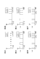


Classifications
-
- H—ELECTRICITY
- H04—ELECTRIC COMMUNICATION TECHNIQUE
- H04B—TRANSMISSION
- H04B10/00—Transmission systems employing electromagnetic waves other than radio-waves, e.g. infrared, visible or ultraviolet light, or employing corpuscular radiation, e.g. quantum communication
- H04B10/07—Arrangements for monitoring or testing transmission systems; Arrangements for fault measurement of transmission systems
- H04B10/075—Arrangements for monitoring or testing transmission systems; Arrangements for fault measurement of transmission systems using an in-service signal
- H04B10/079—Arrangements for monitoring or testing transmission systems; Arrangements for fault measurement of transmission systems using an in-service signal using measurements of the data signal
- H04B10/0795—Performance monitoring; Measurement of transmission parameters
- H04B10/07953—Monitoring or measuring OSNR, BER or Q
-
- H—ELECTRICITY
- H04—ELECTRIC COMMUNICATION TECHNIQUE
- H04B—TRANSMISSION
- H04B10/00—Transmission systems employing electromagnetic waves other than radio-waves, e.g. infrared, visible or ultraviolet light, or employing corpuscular radiation, e.g. quantum communication
- H04B10/40—Transceivers
-
- H—ELECTRICITY
- H04—ELECTRIC COMMUNICATION TECHNIQUE
- H04B—TRANSMISSION
- H04B10/00—Transmission systems employing electromagnetic waves other than radio-waves, e.g. infrared, visible or ultraviolet light, or employing corpuscular radiation, e.g. quantum communication
- H04B10/07—Arrangements for monitoring or testing transmission systems; Arrangements for fault measurement of transmission systems
- H04B10/075—Arrangements for monitoring or testing transmission systems; Arrangements for fault measurement of transmission systems using an in-service signal
-
- H—ELECTRICITY
- H04—ELECTRIC COMMUNICATION TECHNIQUE
- H04B—TRANSMISSION
- H04B10/00—Transmission systems employing electromagnetic waves other than radio-waves, e.g. infrared, visible or ultraviolet light, or employing corpuscular radiation, e.g. quantum communication
- H04B10/11—Arrangements specific to free-space transmission, i.e. transmission through air or vacuum
- H04B10/114—Indoor or close-range type systems
- H04B10/116—Visible light communication
-
- H—ELECTRICITY
- H04—ELECTRIC COMMUNICATION TECHNIQUE
- H04B—TRANSMISSION
- H04B10/00—Transmission systems employing electromagnetic waves other than radio-waves, e.g. infrared, visible or ultraviolet light, or employing corpuscular radiation, e.g. quantum communication
- H04B10/60—Receivers
- H04B10/66—Non-coherent receivers, e.g. using direct detection
- H04B10/69—Electrical arrangements in the receiver
Definitions
- the present invention relates to a method for receiving information in communication using visible light and electromagnetic waves in the peripheral band.
- visible light sources have been used not only for lighting for obtaining light, but also for communication. This has been attributed to the spread of light emitting diodes (LEDs: Light Emitting Diode) as visible light sources.
- LEDs Light Emitting Diode
- a light emitting diode emits less light per element than a conventional visible light source such as an incandescent light bulb or a fluorescent lamp, but is superior to a conventional visible light source in terms of its life, size, and power consumption.
- the light emitting diode has a characteristic that the response speed is very fast in addition to the above characteristics. Further, it is easy to electrically control the light emission of the light emitting diode.
- Non-Patent Document 1 proposes performing communication by superimposing a signal on a household lighting device using a light emitting diode.
- visible light since visible light is not subject to the regulations of the Radio Law, there is no restriction on the band and power, and the band and power can be taken large. Some studies have proposed using it (see, for example, Non-Patent Document 2). Communication performed using a visible light source such as a light emitting diode is referred to as visible light communication.
- a photodetector or an image sensor that is an array thereof is used as a light receiving element of a receiving device.
- signals can usually be obtained continuously.
- an image sensor can acquire a large amount of signals from a photodetector at one time, but due to its nature, it can normally acquire only signals sampled at a predetermined cycle. In this specification, it is assumed that an image sensor is mainly used as a light receiving element.
- FIG. 1 is a block diagram showing a functional configuration of a conventional visible light communication system 900.
- a conventional visible light communication system 900 includes a transmitting device 8 and a receiving device 9.
- the transmitting device 8 includes a modulation unit 81 and a light emitting unit 82.
- the receiving device 9 includes a light receiving unit 91, a synchronization unit 92, and a decoding unit 93.
- the light emitting unit 82 included in the transmitting device 8 includes a light emitting signal control unit 821 and a light emitting element 822.
- the light receiving unit 91 included in the receiving device 9 includes a light receiving element 911.
- the synchronization unit 92 included in the reception device 9 includes a clock element 921, a symbol timing reproduction circuit 922, and a luminance estimation element 923.
- FIG. 2 is a diagram illustrating signals used in the conventional visible light communication system 900
- FIG. 2A is an example of a transmission signal S (i)
- FIG. 2B is an example of a modulation signal M (i)
- FIG. examples of the electrical signal E when the processing time T p 0 (t)
- Fig. 2E when the processing time T p ⁇ 0
- FIG. 2F shows an example of the optical signal F (t) when the processing time T p ⁇ 0.
- the modulation section 81 of the transmitting device 8 receives the digital transmission signal S (i) as an input (see FIG. 2A), modulates the transmission signal S (i), and outputs only 0 or 1 (switch on / off).
- the modulated signal M (i) is output (see FIG. 2B).
- Such a modulation method is called on-off modulation.
- i is an index indicating time, and is an integer indicating a transmission signal number.
- the modulation section 81 generates a sequence M (1), M (2),... Of a sequence S (1), S (2),... Of the input transmission signal S (i). , And outputs a sequence M (1), M (2),... Of the modulated signal M (i).
- Both the transmission signal S (i) and the modulation signal M (i) are 1-bit information.
- ⁇ Transmission device 8 light emission signal control unit 821>
- the light emission signal control unit 821 outputs an electric signal E (t) for driving the light emitting element 822 according to the modulation signal M (i) (see FIG. 2C).
- M (i) is a temporally discrete signal
- E (t) is a temporally continuous signal.
- the light emitting element 822 repeatedly emits and turns off light according to the electric signal E (t), and outputs an optical signal F (t) (see FIG. 2D).
- the output time of the electric signal E (t) corresponding to the time index i is a predetermined time width TTX centered on the time indicated by the index i.
- T TX is referred to as a blink cycle.
- the light emission signal control unit 821 determines that a predetermined time from the time i * T TX -T TX / 2 + T (where T is the delay amount) An electric signal is supplied to the light-emitting element 822 until time i * T TX + T TX / 2 + T when T TX (T ⁇ T TX ) has elapsed.
- T the delay amount
- the delay amount T ( ⁇ T TX / 2).
- the light emitting element 822 emits light according to the electric signal E (t) provided from the light emission signal control unit 821. As a result, the light signal F (t) is output from the light emitting section 82.
- the emission signal control unit 821 may take time to control the light emitting element 822, it may not be possible emission during the processing time T P.
- the input modulation signal M (i) is 1, the time when a predetermined time T TX -T P has elapsed from the time i * T TX -T TX / 2 + T P / 2 + T An electric signal is supplied to the light emitting element 822 until i * T TX + T TX / 2 ⁇ T P / 2 + T.
- the light emitting element 822 outputs an optical signal F (t) according to the electric signal E (t) provided from the light emission signal control unit 821 (see FIG. 2F). By these operations, the light signal F (t) is output from the light emitting section 82.
- the light emitting element 822 outputs an optical signal F (t) according to the electric signal E (t).
- the light emitting element 822 can be, for example, an LED.
- the index i has a predetermined time width TTX .
- a point for example, a center time
- the difference between the times represented by the indexes i and i + 1 is T TX .
- control of the light emitting element 822 may take time. If the time required for processing is T P , the light emission time per index is T TX -T P.
- the light receiving element 911 receives (receives) an optical signal F ′ (t) in which noise is superimposed on the optical signal F (t) output from (the light emitting element 822 of) the transmitting device 8.
- F (t) F '(t)
- the light receiving element 911 is, for example, a photodetector, an image sensor in which photodetectors are arranged in a grid, a high-speed camera, or the like. Further, an optical lens may be provided before the light receiving element 911.
- FIG. 3 is a diagram illustrating a light emitting element and a light receiving element in a conventional visible light communication system 900.
- the light emitting element 822 can be an LED element.
- the light receiving element 911 can be realized as an image sensor including photo detectors 911-a, b, c,.
- the blinking of the light emitting element 822 represented by the index i forms an image on an area ⁇ k on the image sensor (a knitted portion surrounded by a dotted line in FIG. 3) (k is the transmitting device 8). Number).
- the receiving device 9 regards the sum of the output values of all the photodetectors in the region ⁇ k as a reception signal from the k-th transmitting device 8.
- ⁇ Receiver 9 When transmitting information on a communication channel, it is general to encode the original information in some form.
- the signal of the minimum unit constituting the encoded information is called a symbol.
- a clock of a symbol (information indicating a time width used when transmitting one symbol) of a symbol of the transmission device is received so that a decoding device correctly decodes encoded information transmitted from the transmission device. It is important to detect on the device side. This is called symbol clock synchronization between the receiving device and the transmitting device. It is desirable that the symbol clock synchronization is always performed during communication. This is because there is generally no means for sharing the same oscillator between the receiving apparatus and the transmitting apparatus, and therefore, there is a possibility that synchronization is always shifted.
- Synchronization unit 92 estimates the parameter (parameter of the out-of-sync parameter g c and the maximum brightness R) needed to decode the optical signal F transmitted (t) correctly from the transmission device 8 to output. Specifically, parameters (g c , R) necessary for decoding are generated by the following operations of the clock element 921, the symbol timing reproduction circuit 922, and the luminance estimation element 923.
- ⁇ Receiver 9 Clock element 921>
- the clock element 921 generates a clock.
- Symbol timing reproduction circuit 922 uses the clock obtained from the clock element 921 and the electric signal E ′ (t) obtained from (the light receiving element 911 of) the light receiving section 91 to generate the clock of the clock element 921 and the clock of the transmitting device 8. obtains and outputs a parameter g c representing a synchronization deviation between. It is known that the symbol timing reproducing circuit 922 detects the phase difference between two input signals and performs feedback control to synchronize the phases. In this symbol timing reproduction circuit, one of two input signals is an input from an oscillator, and the other is a signal to be synchronized.
- Luminance estimation element 923 estimates a parameter R representing the maximum luminance (hereinafter, also referred to as “maximum luminance value”) using the electric signal E ′ (t) obtained from (the light receiving element 911 of) the light receiving section 91.
- ⁇ Receiving device 9 decoding unit 93> Decoding unit 93, an electric signal E outputted from the light receiving portion 91 (light receiving element 911) '(t), the least square method clues and a parameter R indicating the parameter g c and the maximum brightness that represents the synchronization error And decodes the result, and outputs a decoding result M ′ (j).
- the receiving device 9 may be provided with a demodulation unit (not shown), and the demodulation unit may demodulate the decoding result M ′ (j) and output the demodulation result S ′ (j).
- the demodulation unit needs to be configured to correspond to the modulation unit 81.
- the obtained signal is a sampled signal (discrete time signal).
- a certain large sampling frequency is required to perform symbol clock synchronization by the symbol timing recovery circuit. That is, in order to reconstruct a signal in order to use the symbol timing recovery circuit, there is a problem that a sampling frequency higher than a sampling frequency originally required for communication is required.
- the throughput (the amount of data transmitted per unit time) between the image sensor and a general processing device at the subsequent stage is generally limited.
- the activation frequency cannot exceed a certain value. For this reason, if the sampling frequency is to be increased, the number of pixels must be reduced, and as a result, the number of transmitting devices that can be received by one receiving device must be reduced.
- the blinking cycle of the transmitter must be increased (the blinking frequency must be reduced) in order to perform accurate symbol clock synchronization.
- an object of the present invention is to provide a receiving apparatus capable of reducing a sampling frequency required for symbol timing reproduction as compared with the related art.
- a receiving device is a receiving device that performs visible light communication with a transmitting device, and the intensity of an electric signal corresponding to an optical signal received from the transmitting device is set to a predetermined value.
- a received signal generation unit that measures the received signal at each time interval to generate a received signal sequence, and using a distribution of the received signal estimated from the received signal sequence, a maximum luminance value, a synchronization shift, and at least a steady noise level.
- a parameter estimator for estimating at least one parameter including the maximum luminance value.
- the sampling frequency required for symbol timing reproduction can be made smaller than before.
- FIG. 1 is a diagram illustrating a functional configuration of a conventional visible light communication system.
- FIG. 2 is a diagram illustrating a signal transmitted by visible light communication.
- FIG. 3 is a diagram illustrating a light emitting element and a light receiving element.
- FIG. 4 is a diagram illustrating a functional configuration of the visible light communication system according to the embodiment.
- FIG. 5 is a diagram illustrating an operation of the visible light communication system according to the embodiment.
- FIG. 6 is a diagram illustrating a signal received by visible light communication.
- FIG. 4 is a block diagram illustrating a functional configuration of the visible light communication system 100 according to the first embodiment.
- the visible light communication system 100 according to the first embodiment includes a transmitting device 8 and a receiving device 1.
- the transmitting device 8 is the same as the transmitting device 8 included in the conventional visible light communication system 900 described above.
- the receiving device 1 includes a light receiving unit 11, a parameter estimating unit 12, and a decoding unit 13.
- the light receiving unit 11 included in the receiving device 1 includes a light receiving element 111 and a received signal generating unit 112.
- the parameter estimation unit 12 included in the receiving device 1 includes a reception signal distribution estimation unit 121 and a distribution estimation result interpretation unit 122.
- the visible light communication method of the first embodiment is realized by the visible light communication system 100 performing the processing of each step shown in FIG.
- a series of steps executed by the receiving device 1 in the visible light communication method according to the first embodiment is referred to as a receiving method according to the first embodiment.
- the receiving device 1 is, for example, a special or special computer configured by reading a special program into a known or dedicated computer having a central processing unit (CPU: Central Processing Unit), a main storage device (RAM: Random Access Memory), and the like. Device.
- the receiving device 1 executes each process under the control of the central processing unit, for example.
- the data input to the receiving device 1 and the data obtained in each process are stored in, for example, a main storage device, and the data stored in the main storage device is read out to a central processing unit as needed, and Used for processing.
- At least a part of each processing unit of the receiving device 1 may be configured by hardware such as an integrated circuit.
- a measurement cycle (hereinafter, also referred to as a “sampling cycle”) of the reception signal generation unit 112, which will be described later, is T RX , and an exposure time of the light receiving element 111 is ⁇ .
- the light receiving element 111 can be, for example, a photodetector as in the related art. Further, an optical lens may be provided in a stage preceding the light receiving element 111. Further, the light receiving element 111 may be an image sensor in which photo detectors are arranged in a lattice.
- the reception signal generation unit 112 includes a sampling element, a memory, an arithmetic unit, and the like.
- the light receiving element 111 receives the optical signal F ′ (t) in which noise is superimposed on the optical signal F (t) output from the transmitting device 8, and receives an electric signal E ′ (t) corresponding to the optical signal F ′ (t). t) is output to the reception signal generation unit 112 (step S111).
- Received signal generator 112 measures the intensity of the electric signal E ′ (t) at predetermined time intervals T RX ( ⁇ T TX ) (step S112).
- the reception signal generation unit 112 outputs the time g c * ⁇ + j * T RX -T RX / 2 ⁇ / 2 to g c * ⁇ + j as shown in FIG. * T RX -T RX / 2 + ⁇ / 2
- the charge accumulated in the sampling element is measured, and the measurement result is output as a series of reception signals B ′ (j) for each index j.
- the reception signal generation unit 112 outputs g c * ⁇ + j * T RX -T RX / 2 ⁇ / 2 to g c at each photodetector.
- * ⁇ + j * T RX -T RX / 2 + ⁇ / 2 Measure the charge accumulated in the sampling element and add the measurement result in the predetermined range ⁇ k It is output as a sequence of the received signal B '(j).
- the parameter estimating unit 12 includes a memory, an arithmetic device, and the like.
- the parameter estimating unit 12 obtains the sequence of the received signal B ′ (j) from the received signal generating unit 112, and uses the received signal distribution estimating unit 121 and the distribution estimation result interpreting unit 122 to obtain the maximum luminance parameter R and the synchronization deviation. among the parameters g c and the constant noise level parameters d, estimating one or more parameters or including parameters R of at least the maximum brightness, and outputs the same to the decoder 13.
- Received signal distribution estimator 121 receives the received signal B ′ (j) and sequentially stores it in the memory. Next, the signal distribution estimating unit 121 estimates the distribution of the received signals from the histogram of the J received signals B ′ (j), B ′ (j + 1),. S121).
- J is an amount determined according to the blinking period T TX , the measurement period T RX , the exposure time ⁇ , the magnitude of the non-stationary noise, and the like. Since the reception signal B ′ (j) corresponds to the luminance at the time indicated by the time index j, the distribution of the reception signal is a distribution representing the frequency of each luminance of the reception signal.
- Distribution estimation result interpreting unit 122 Distribution estimation result interpretation unit 122, a parameter d of the parameters R and sync parameter g c and the constant noise level of the maximum luminance in a model of equation (1) from distribution of the received signal the received signal distribution estimating unit 121 estimates Estimate and output (step S122).
- B '(j) R (g c * S (i) + (1-g c ) * S (i + 1)) + d (1)
- the above parameters R, g c , and d are obtained from the average of each of 2 to 4 peaks appearing in the histogram of the received signal.
- step S ⁇ b > 13 the decoding unit 13 determines whether the reception signal output from the reception signal generation unit 112 is based on the maximum luminance parameter R, the synchronization shift parameter gc, and the stationary noise level parameter d output from the parameter estimation unit 12.
- the signal B ′ (j) is decoded, and a decoding result M ′ (j) is output.
- the decoding method is the same as that of the decoding unit 93 of the conventional receiving device 9.
- a demodulation unit (not shown) may be provided similarly to the above-described conventional receiving device 9, and the demodulation unit may demodulate the decoding result M ′ (j) and output the demodulation result S ′ (j). In this case, the demodulation unit needs to be configured to correspond to the modulation unit 81.
- the visible light communication system of the present invention can be configured.
- a plurality of sets (a total of H sets) of the light receiving unit 11, the parameter estimating unit 12, and the decoding unit 13 corresponding to each transmitting device 8 may be prepared.
- the parameter d of the parameters R and sync parameter g c and the constant noise level of the maximum luminance is calculated corresponding to each of the transmission device 8.
- a program describing this processing content can be recorded on a computer-readable recording medium.
- a computer-readable recording medium for example, any recording medium such as a magnetic recording device, an optical disk, a magneto-optical recording medium, and a semiconductor memory may be used.
- the distribution of the program is performed by selling, transferring, lending, or the like, a portable recording medium such as a DVD or a CD-ROM on which the program is recorded.
- the program may be stored in a storage device of a server computer, and the program may be distributed by transferring the program from the server computer to another computer via a network.
- the computer that executes such a program first stores, for example, a program recorded on a portable recording medium or a program transferred from a server computer in its own storage device. Then, when executing the processing, the computer reads the program stored in its own storage device and executes the processing according to the read program. Further, as another execution form of the program, the computer may directly read the program from the portable recording medium and execute processing according to the program, and further, the program may be transferred from the server computer to the computer. Each time, the processing according to the received program may be sequentially executed.
- the program in the present embodiment includes information used for processing by the computer and which is similar to the program (data that is not a direct command to the computer but has characteristics that define the processing of the computer).
- the present apparatus is configured by executing a predetermined program on a computer, but at least a part of the processing contents may be realized by hardware.
Landscapes
- Physics & Mathematics (AREA)
- Electromagnetism (AREA)
- Engineering & Computer Science (AREA)
- Computer Networks & Wireless Communication (AREA)
- Signal Processing (AREA)
- Optical Communication System (AREA)
Abstract
シンボルタイミング再生に要する標本化周波数を従来よりも小さくする。受信装置1は送信装置8と可視光通信をする。受信信号生成部112は送信装置8から受信した光信号に対応する電気信号の強度を所定の時間間隔毎に計測して受信信号の系列を生成する。パラメータ推定部12は受信信号の系列から推定した受信信号の分布を用いて、最大輝度値、同期ずれ、および定常ノイズレベルのうち、少なくとも最大輝度値を含むいずれか1つ以上のパラメータを推定する。
Description
この発明は可視光およびその周辺帯域の電磁波を用いた通信における情報の受信方法に関するものである。
近年、可視光源は明かりを得るための照明用途のみならず通信用途にも用いられている。これは可視光源として発光ダイオード(LED: Light Emitting Diode)の普及が進んだことが寄与している。発光ダイオードは素子1つあたりの発光量は白熱電球や蛍光灯などの従来の可視光源には及ばないものの、その寿命や大きさおよび消費電力の面で従来の可視光源に対して優れている。発光ダイオードは上記のような特徴に加え、応答速度が非常に速いという特性を持つ。また、発光ダイオードの発光を電気的に制御することは容易である。発光ダイオードには上記のような特性があるため、近年では明かりを得るための照明用途のみならず、可視光の点滅を利用した信号伝送用途に用いるための研究開発が行われている。例えば非特許文献1では発光ダイオードを用いた家庭用照明器具に信号を重畳させて通信を行うことを提案している。また、現在のところ可視光は電波法の規制の対象外であることから帯域や電力の制限がなく、帯域や電力を大きく取ることができるため、このことを利用して発光ダイオードを通信専用に用いることを提案している研究もある(例えば、非特許文献2参照)。発光ダイオードなどの可視光源を用いて行う通信を可視光通信と呼ぶ。可視光通信では受信装置の受光素子としてフォトディテクタあるいはそのアレーであるイメージセンサを用いる。フォトディテクタでは通常、信号を連続的に得ることができる。一方で、イメージセンサは大量のフォトディテクタからの信号を一度に取得できるが、その性質上通常は所定の周期で標本化された信号のみ取得可能である。本明細書においては、受光素子として主にイメージセンサを用いることを想定する。
以下、図1を参照して従来の可視光通信システムについて概説する。図1は、従来の可視光通信システム900の機能構成を示すブロック図である。図1に示すとおり、従来の可視光通信システム900は、送信装置8と受信装置9とからなる。送信装置8は、変調部81と発光部82とを備える。受信装置9は、受光部91と同期部92と復号部93とを備える。送信装置8が備える発光部82は、発光信号制御部821と発光素子822とを備える。受信装置9が備える受光部91は、受光素子911を備える。受信装置9が備える同期部92は、クロック素子921とシンボルタイミング再生回路922と輝度推定素子923とを備える。
以下、図2を参照して図1に示す可視光通信システム900において使用される信号について説明する。図2は従来の可視光通信システム900で使用される信号を例示する図であって、図2Aは伝送信号S(i)の例、図2Bは変調信号M(i)の例、図2Cは処理時間Tp=0の場合の電気信号E(t)の例、図2Dは処理時間Tp=0の場合の光信号F(t)の例、図2Eは処理時間Tp≠0の場合の電気信号E(t)の例、図2Fは処理時間Tp≠0の場合の光信号F(t)の例をそれぞれ示す。
<送信装置8:変調部81>
送信装置8の変調部81は、ディジタルの伝送信号S(i)を入力として(図2A参照)、当該伝送信号S(i)を変調し、0または1のみ(スイッチがオンかオフか)の変調信号M(i)を出力する(図2B参照)。このような変調方法をオンオフ変調と呼ぶ。ここで、iは時間を示すインデックスであり、伝送信号の番号を表す整数とする。変調部81は、入力された伝送信号S(i)の系列S(1), S(2), …の変調信号M(i)の系列M(1), M(2), …を生成し、当該変調信号M(i)の系列M(1), M(2), …を出力する。伝送信号S(i)、変調信号M(i)はともに1ビットの情報である。
送信装置8の変調部81は、ディジタルの伝送信号S(i)を入力として(図2A参照)、当該伝送信号S(i)を変調し、0または1のみ(スイッチがオンかオフか)の変調信号M(i)を出力する(図2B参照)。このような変調方法をオンオフ変調と呼ぶ。ここで、iは時間を示すインデックスであり、伝送信号の番号を表す整数とする。変調部81は、入力された伝送信号S(i)の系列S(1), S(2), …の変調信号M(i)の系列M(1), M(2), …を生成し、当該変調信号M(i)の系列M(1), M(2), …を出力する。伝送信号S(i)、変調信号M(i)はともに1ビットの情報である。
例えば、伝送信号の系列がS(1)=0, S(2)=1, S(3)=1, S(4)=1であった場合、変調結果はM(1)=0, M(2)=1, M(3)=1, M(4)=1となる。
<送信装置8:発光信号制御部821>
発光信号制御部821は変調信号M(i)に従って発光素子822を駆動するための電気信号E(t)を出力する(図2C参照)。ただし、M(i)は時間的に離散的な信号であるのに対して、E(t)は時間的に連続的な信号である。発光素子822は電気信号E(t)に従い発光・消灯を繰り返し、光信号F(t)を出力する(図2D参照)。時間のインデックスiに相当する電気信号E(t)の出力時間はインデックスiで示される時刻を中心とする所定の時間幅TTXとする。以下ではTTXを点滅周期と呼ぶ。
発光信号制御部821は変調信号M(i)に従って発光素子822を駆動するための電気信号E(t)を出力する(図2C参照)。ただし、M(i)は時間的に離散的な信号であるのに対して、E(t)は時間的に連続的な信号である。発光素子822は電気信号E(t)に従い発光・消灯を繰り返し、光信号F(t)を出力する(図2D参照)。時間のインデックスiに相当する電気信号E(t)の出力時間はインデックスiで示される時刻を中心とする所定の時間幅TTXとする。以下ではTTXを点滅周期と呼ぶ。
具体的には、発光信号制御部821は、入力された変調信号M(i)が1である場合は、時刻i*TTX-TTX/2+T(ただしTは遅延量)から所定時間TTX(T≦TTX)経過した時刻i*TTX+TTX/2+Tまでの間、発光素子822に電気信号を与える。入力された変調信号M(i)が0である場合は、時刻i*TTX-TTX/2+Tから所定時間TTX経過した時刻i*TTX+TTX/2+Tまでの間、発光素子822には電気信号を与えない。なお、図2の例では、遅延量T=(-TTX/2)である。発光素子822は発光信号制御部821から与えられた電気信号E(t)により発光する。これらにより、発光部82から光信号F(t)が出力される。
発光信号制御部821の性能によっては発光素子822の制御に時間を要する場合があり、その処理時間TPの間発光できない場合がある。そのような場合は、入力された変調信号M(i)が1である場合は、時刻i*TTX-TTX/2+TP/2+Tから所定時間TTX-TP経過した時刻i*TTX+TTX/2-TP/2+Tまでの間、発光素子822に電気信号を与える。入力された変調信号M(i)が0である場合は、時刻i*TTX-TTX/2+TP/2+Tから所定時間TTX-TP経過した時刻i*TTX+TTX/2-TP/2+Tまでの間、発光素子822には電気信号を与えない(図2E参照)。発光素子822は発光信号制御部821から与えられた電気信号E(t)に従って光信号F(t)を出力する(図2F参照)。これらの動作により、発光部82から光信号F(t)が出力される。
<送信装置8:発光素子822>
発光素子822は電気信号E(t)に従って光信号F(t)を出力する。発光素子822は例えばLEDとすることができる。なお、図2Dに示すように、インデックスiは所定の時間幅TTXを持つ。ただし、時間的に離散的な信号を表す場合はインデックスiの示す時間幅のある一点(例えば中心の時刻)をやはりiによって表す。例えば離散的な信号を表す場合、インデックスiとi+1で表される時間の差はTTXとなる。また、遅延だけでなく図2Fに示すように、発光素子822の制御に時間を要する場合があり、処理に要する時間をTPとおくとインデックスあたりの発光時間はTTX-TPとなる。
発光素子822は電気信号E(t)に従って光信号F(t)を出力する。発光素子822は例えばLEDとすることができる。なお、図2Dに示すように、インデックスiは所定の時間幅TTXを持つ。ただし、時間的に離散的な信号を表す場合はインデックスiの示す時間幅のある一点(例えば中心の時刻)をやはりiによって表す。例えば離散的な信号を表す場合、インデックスiとi+1で表される時間の差はTTXとなる。また、遅延だけでなく図2Fに示すように、発光素子822の制御に時間を要する場合があり、処理に要する時間をTPとおくとインデックスあたりの発光時間はTTX-TPとなる。
<受信装置9:受光素子911>
受光素子911は送信装置8(の発光素子822)から出力された光信号F(t)にノイズが重畳した光信号F'(t)を受信(受光)する。理想的にはF(t)=F'(t)であるが,フォトディテクタの性能や遅延により変化する場合もあるので、ここではF(t)とF'(t)とを分けて記述する。おおよそF'(t+T)=F'(t)であることが想定される。受光素子911は、例えばフォトディテクタやフォトディテクタを格子状に並べたイメージセンサや高速カメラ等である。また、受光素子911の前段に光学レンズを設けてもよい。
受光素子911は送信装置8(の発光素子822)から出力された光信号F(t)にノイズが重畳した光信号F'(t)を受信(受光)する。理想的にはF(t)=F'(t)であるが,フォトディテクタの性能や遅延により変化する場合もあるので、ここではF(t)とF'(t)とを分けて記述する。おおよそF'(t+T)=F'(t)であることが想定される。受光素子911は、例えばフォトディテクタやフォトディテクタを格子状に並べたイメージセンサや高速カメラ等である。また、受光素子911の前段に光学レンズを設けてもよい。
図3を参照して従来の可視光通信システム900における発光素子、受光素子の実現例について説明する。図3は従来の可視光通信システム900における発光素子、受光素子を例示する図である。図3に示すように、従来の可視光通信システム900においては、例えば発光素子822をLED素子とすることができる。また受光素子911をフォトディテクタ911-a,b,c,…よりなるイメージセンサとして実現することができる。図3に示すように、インデックスiで表される発光素子822の点滅がイメージセンサ上の領域Ωk(図3において点線で囲まれた編み掛け部分)に結像するとする(kは送信装置8の番号)。受信装置9は領域Ωkのすべてのフォトディテクタの出力値の合計をk番目の送信装置8からの受信信号として捉える。
<受信装置9:同期部92>
通信路において情報を伝送する際には元の情報を何らかのかたちで符号化することが一般的である。符号化された情報を構成する最小単位の信号をシンボルと呼ぶ。ディジタル通信路では、送信装置から送信される符号化された情報を復号装置で正しく復号するために送信装置のシンボルのクロック(1つのシンボルを伝送する際に使用する時間幅を表す情報)を受信装置側で検出することが重要である。これを行うことを受信装置と送信装置の間でのシンボルクロック同期という。シンボルクロック同期は通信をしている間常に行われていることが望ましい。これは、一般に受信装置と送信装置の間で同じ発振器を共有する手段がないため、同期が常にずれてしまう可能性があるからである。
通信路において情報を伝送する際には元の情報を何らかのかたちで符号化することが一般的である。符号化された情報を構成する最小単位の信号をシンボルと呼ぶ。ディジタル通信路では、送信装置から送信される符号化された情報を復号装置で正しく復号するために送信装置のシンボルのクロック(1つのシンボルを伝送する際に使用する時間幅を表す情報)を受信装置側で検出することが重要である。これを行うことを受信装置と送信装置の間でのシンボルクロック同期という。シンボルクロック同期は通信をしている間常に行われていることが望ましい。これは、一般に受信装置と送信装置の間で同じ発振器を共有する手段がないため、同期が常にずれてしまう可能性があるからである。
同期部92は、送信装置8から送信された光信号F(t)を正しく復号するために必要なパラメータ(同期ずれのパラメータgcと最大輝度のパラメータR)を推定し、出力する。具体的には、クロック素子921、シンボルタイミング再生回路922、および輝度推定素子923の以下の動作により、復号に必要なパラメータ(gc, R)が生成される。
<受信装置9:クロック素子921>
クロック素子921は、クロックを発生する。
クロック素子921は、クロックを発生する。
<受信装置9:シンボルタイミング再生回路922>
シンボルタイミング再生回路922は、クロック素子921から取得したクロックと受光部91(の受光素子911)から得た電気信号E'(t)とを用いて、クロック素子921のクロックと送信装置8のクロックとの同期ずれを表すパラメータgcを求めて出力する。シンボルタイミング再生回路922は、入力された2つの信号の位相差を検出しフィードバック制御をかけることで位相を同期させるものが知られている。このシンボルタイミング再生回路は、入力される2つの信号のうち片方が発振器からの入力であり、もう片方が同期させたい信号である。
シンボルタイミング再生回路922は、クロック素子921から取得したクロックと受光部91(の受光素子911)から得た電気信号E'(t)とを用いて、クロック素子921のクロックと送信装置8のクロックとの同期ずれを表すパラメータgcを求めて出力する。シンボルタイミング再生回路922は、入力された2つの信号の位相差を検出しフィードバック制御をかけることで位相を同期させるものが知られている。このシンボルタイミング再生回路は、入力される2つの信号のうち片方が発振器からの入力であり、もう片方が同期させたい信号である。
<受信装置9:輝度推定素子923>
輝度推定素子923は、受光部91(の受光素子911)から得た電気信号E'(t)を用いて、最大輝度を表すパラメータ(以下、「最大輝度値」ともいう)Rを推定する。
輝度推定素子923は、受光部91(の受光素子911)から得た電気信号E'(t)を用いて、最大輝度を表すパラメータ(以下、「最大輝度値」ともいう)Rを推定する。
<受信装置9:復号部93>
復号部93は、受光部91(の受光素子911)から出力された電気信号E'(t)を、同期ずれを表すパラメータgcと最大輝度を表すパラメータRとを手掛かりに最小二乗法などを用いて復号し、復号結果M'(j)を出力する。ここで、jは時間を示すインデックスであり、通常i=jである。電気信号E'(t)を何らかのかたちで離散化することで最小二乗法をディジタル回路で行うことができる。なお、受信装置9に図示していない復調部を設け、復調部が復号結果M'(j)を復調して復調結果S'(j)を出力する構成としてもよい。この場合復調部は変調部81と対応するように構成されている必要がある。
復号部93は、受光部91(の受光素子911)から出力された電気信号E'(t)を、同期ずれを表すパラメータgcと最大輝度を表すパラメータRとを手掛かりに最小二乗法などを用いて復号し、復号結果M'(j)を出力する。ここで、jは時間を示すインデックスであり、通常i=jである。電気信号E'(t)を何らかのかたちで離散化することで最小二乗法をディジタル回路で行うことができる。なお、受信装置9に図示していない復調部を設け、復調部が復号結果M'(j)を復調して復調結果S'(j)を出力する構成としてもよい。この場合復調部は変調部81と対応するように構成されている必要がある。
小峯敏彦、田中裕一、中川正雄、「白色LED照明信号伝送と電力線信号伝送の融合システム」、電子情報通信学会技術研究報告、社団法人電子情報通信学会、2002年3月12日、Vol. 101、No. 726、pp.99-104
石田正徳、春山真一郎、中川正雄、「並列可視光無線通信方式における通信速度限界の検討」、電子情報通信学会技術研究報告.CS 通信方式、社団法人電子情報通信学会、2007年1月4日、Vol. 106、No. 450、pp. 37-41
受光素子としてフォトディテクタを用いる場合、信号を連続的に得ることができるので、上述した従来のシンボルタイミング再生回路を用いることは容易である。しかしながら、ディジタル回路によってシンボルクロック同期を行うことが望まれる場合においては、ある程度大きな標本化周波数が必要となる。
一方で、受光素子としてイメージセンサを用いる場合、得られる信号は標本化された信号(離散時間信号)となる。この場合は、シンボルタイミング再生回路によるシンボルクロック同期を行うためには、ある程度の大きな標本化周波数が必要である。つまり、シンボルタイミング再生回路を用いるために信号を再構成するためには、本来通信に必要な標本化周波数よりも大きな標本化周波数が必要になるという問題があった。
さらに、受光素子としてイメージセンサを用いた場合、一般的にイメージセンサと後段の一般の処理装置との間のスループット(単位時間当たりのデータ伝送量)には限界があるために、画素数×標本化周波数は一定の値を上回ることができない。このため、標本化周波数を上げようとすれば、画素数を絞らざるを得なくなり、その結果一つの受信装置が受信することができる送信装置の数を減らさざるを得ない。一方、標本化周波数に上限がある受信装置を用いた場合、正確なシンボルクロック同期を行うためには送信機の点滅周期を大きく(点滅周波数を小さく)せざるを得ない。
この発明は、上記のような技術的課題に鑑みて、シンボルタイミング再生に要する標本化周波数を従来よりも小さくすることができる受信装置を提供することを目的とする。
上記の課題を解決するために、この発明の一態様の受信装置は、送信装置と可視光通信をする受信装置であって、送信装置から受信した光信号に対応する電気信号の強度を所定の時間間隔毎に計測して受信信号の系列を生成する受信信号生成部と、受信信号の系列から推定した受信信号の分布を用いて、最大輝度値、同期ずれ、および定常ノイズレベルのうち、少なくとも最大輝度値を含むいずれか1つ以上のパラメータを推定するパラメータ推定部と、を含む。
この発明によれば、シンボルタイミング再生に要する標本化周波数を従来よりも小さくすることができる。
以下、この発明の実施の形態について詳細に説明する。なお、図面中において同じ機能を有する構成部には同じ番号を付し、重複説明を省略する。
[第一実施形態]
図4は、第一実施形態の可視光通信システム100の機能構成を示すブロック図である。図4に示すとおり、第一実施形態の可視光通信システム100は、送信装置8と受信装置1とからなる。送信装置8は上述した従来の可視光通信システム900に含まれる送信装置8と同じものである。受信装置1は、受光部11とパラメータ推定部12と復号部13とを備える。受信装置1が備える受光部11は、受光素子111と受信信号生成部112とを備える。受信装置1が備えるパラメータ推定部12は、受信信号分布推定部121と分布推定結果解釈部122とを備える。この可視光通信システム100が、図5に示す各ステップの処理を行うことにより第一実施形態の可視光通信方法が実現される。なお、第一実施形態の可視光通信方法のうち受信装置1が実行する一連のステップを第一実施形態の受信方法とする。
図4は、第一実施形態の可視光通信システム100の機能構成を示すブロック図である。図4に示すとおり、第一実施形態の可視光通信システム100は、送信装置8と受信装置1とからなる。送信装置8は上述した従来の可視光通信システム900に含まれる送信装置8と同じものである。受信装置1は、受光部11とパラメータ推定部12と復号部13とを備える。受信装置1が備える受光部11は、受光素子111と受信信号生成部112とを備える。受信装置1が備えるパラメータ推定部12は、受信信号分布推定部121と分布推定結果解釈部122とを備える。この可視光通信システム100が、図5に示す各ステップの処理を行うことにより第一実施形態の可視光通信方法が実現される。なお、第一実施形態の可視光通信方法のうち受信装置1が実行する一連のステップを第一実施形態の受信方法とする。
受信装置1は、例えば、中央演算処理装置(CPU: Central Processing Unit)、主記憶装置(RAM: Random Access Memory)などを有する公知又は専用のコンピュータに特別なプログラムが読み込まれて構成された特別な装置である。受信装置1は、例えば、中央演算処理装置の制御のもとで各処理を実行する。受信装置1に入力されたデータや各処理で得られたデータは、例えば、主記憶装置に格納され、主記憶装置に格納されたデータは必要に応じて中央演算処理装置へ読み出されて他の処理に利用される。受信装置1の各処理部は、少なくとも一部が集積回路等のハードウェアによって構成されていてもよい。
以下、後述する受信信号生成部112の計測周期(以下「標本化周期」ともいう)をTRX、受光素子111の露光時間をτとし、本実施形態では点滅周期TTXと計測周期TRXがほぼ等しく(TTX≒TRX)、かつ処理時間TP=0である場合について説明する。
<受信装置1:受光部11>
受光素子111は、従来技術と同じく例えばフォトディテクタとすることができる。また、受光素子111の前段に光学レンズを設けてもよい。さらに、受光素子111はフォトディテクタを格子状に並べたイメージセンサでもよい。受信信号生成部112は標本化素子、メモリ、演算装置などからなる。
受光素子111は、従来技術と同じく例えばフォトディテクタとすることができる。また、受光素子111の前段に光学レンズを設けてもよい。さらに、受光素子111はフォトディテクタを格子状に並べたイメージセンサでもよい。受信信号生成部112は標本化素子、メモリ、演算装置などからなる。
<受信装置1:受光素子111>
受光素子111は、送信装置8から出力された光信号F(t)にノイズが重畳した光信号F'(t)を受信して、光信号F'(t)に対応する電気信号E'(t)を受信信号生成部112に対して出力する(ステップS111)。
受光素子111は、送信装置8から出力された光信号F(t)にノイズが重畳した光信号F'(t)を受信して、光信号F'(t)に対応する電気信号E'(t)を受信信号生成部112に対して出力する(ステップS111)。
<受信装置1:受信信号生成部112>
受信信号生成部112は、電気信号E'(t)の強度を所定の時間間隔TRX(≒TTX)毎に計測する(ステップS112)。受光素子111が単独のフォトディテクタの場合、受信信号生成部112は、図6に示すように、時刻gc*τ+j*TRX-TRX/2-τ/2からgc*τ+j*TRX-TRX/2+τ/2までに標本化素子に蓄積された電荷を計測し、計測結果をインデックスj毎の受信信号B'(j)の系列として出力する。一方、受光素子111がイメージセンサの場合、受信信号生成部112は、図6に示すように、各フォトディテクタで時刻gc*τ+j*TRX-TRX/2-τ/2からgc*τ+j*TRX-TRX/2+τ/2までに標本化素子に蓄積された電荷を計測し、予め定められた範囲Ωk内の計測結果を加算した結果をインデックスj毎の受信信号B'(j)の系列として出力する。
受信信号生成部112は、電気信号E'(t)の強度を所定の時間間隔TRX(≒TTX)毎に計測する(ステップS112)。受光素子111が単独のフォトディテクタの場合、受信信号生成部112は、図6に示すように、時刻gc*τ+j*TRX-TRX/2-τ/2からgc*τ+j*TRX-TRX/2+τ/2までに標本化素子に蓄積された電荷を計測し、計測結果をインデックスj毎の受信信号B'(j)の系列として出力する。一方、受光素子111がイメージセンサの場合、受信信号生成部112は、図6に示すように、各フォトディテクタで時刻gc*τ+j*TRX-TRX/2-τ/2からgc*τ+j*TRX-TRX/2+τ/2までに標本化素子に蓄積された電荷を計測し、予め定められた範囲Ωk内の計測結果を加算した結果をインデックスj毎の受信信号B'(j)の系列として出力する。
<受信装置1:パラメータ推定部12>
パラメータ推定部12はメモリ、演算装置などからなる。パラメータ推定部12は受信信号生成部112から受信信号B'(j)の系列を取得し、受信信号分布推定部121および分布推定結果解釈部122を用いて、最大輝度のパラメータRと同期ずれのパラメータgcと定常ノイズレベルのパラメータdとのうち、少なくとも最大輝度のパラメータRを含むいずれか1以上のパラメータを推定し、復号部13に対して出力する。
パラメータ推定部12はメモリ、演算装置などからなる。パラメータ推定部12は受信信号生成部112から受信信号B'(j)の系列を取得し、受信信号分布推定部121および分布推定結果解釈部122を用いて、最大輝度のパラメータRと同期ずれのパラメータgcと定常ノイズレベルのパラメータdとのうち、少なくとも最大輝度のパラメータRを含むいずれか1以上のパラメータを推定し、復号部13に対して出力する。
<受信装置1:受信信号分布推定部121>
信号分布推定部121は、受信信号B'(j)を入力とし、順次メモリに格納する。次に、信号分布推定部121は、J個の受信信号B'(j), B'(j+1), …, B'(j+J)のヒストグラムから受信信号の分布を推定する(ステップS121)。ここで、Jは点滅周期TTX、計測周期TRX、露光時間τ、および非定常ノイズの大きさなどに合わせて決まる量である。受信信号B'(j)は時間のインデックスjが示す時刻における輝度に対応するため、受信信号の分布は受信信号の輝度毎の頻度を表す分布である。
信号分布推定部121は、受信信号B'(j)を入力とし、順次メモリに格納する。次に、信号分布推定部121は、J個の受信信号B'(j), B'(j+1), …, B'(j+J)のヒストグラムから受信信号の分布を推定する(ステップS121)。ここで、Jは点滅周期TTX、計測周期TRX、露光時間τ、および非定常ノイズの大きさなどに合わせて決まる量である。受信信号B'(j)は時間のインデックスjが示す時刻における輝度に対応するため、受信信号の分布は受信信号の輝度毎の頻度を表す分布である。
<受信装置1:分布推定結果解釈部122>
分布推定結果解釈部122は、受信信号分布推定部121が推定した受信信号の分布から式(1)のモデルにおける最大輝度のパラメータRと同期ずれのパラメータgcと定常ノイズレベルのパラメータdとを推定し、出力する(ステップS122)。
B'(j)=R(gc*S(i)+(1-gc)*S(i+1))+d …(1)
分布推定結果解釈部122は、受信信号分布推定部121が推定した受信信号の分布から式(1)のモデルにおける最大輝度のパラメータRと同期ずれのパラメータgcと定常ノイズレベルのパラメータdとを推定し、出力する(ステップS122)。
B'(j)=R(gc*S(i)+(1-gc)*S(i+1))+d …(1)
より具体的には、伝送信号S(i), S(i+1)がそれぞれ0または1を取ることから、ノイズがない場合は受信信号B'(j)の取り得る値が、d(S(i)=0かつS(i+1)=0の場合)、R*gc+d(S(i)=1かつS(i+1)=0の場合)、R(1-gc)+d(S(i)=0かつS(i+1)=1の場合)、R+d(S(i)=1かつS(i+1)=1の場合)の4種類のいずれかとなる。これを利用して、受信信号のヒストグラムに現れる2~4個のピークそれぞれの平均から、上記のパラメータR, gc, dを求める。
<受信装置1:復号部13>
ステップS13において、復号部13は、パラメータ推定部12が出力する最大輝度のパラメータRと同期ずれのパラメータgcと定常ノイズレベルのパラメータdとに基づいて、受信信号生成部112から出力された受信信号B'(j)を復号し、復号結果M'(j)を出力する。復号の方法は、従来の受信装置9の復号部93と同様である。上述した従来の受信装置9と同様に図示していない復調部を設け、復調部が復号結果M'(j)を復調して復調結果S'(j)を出力する構成としてもよい。この場合復調部は変調部81と対応するように構成されている必要がある。
ステップS13において、復号部13は、パラメータ推定部12が出力する最大輝度のパラメータRと同期ずれのパラメータgcと定常ノイズレベルのパラメータdとに基づいて、受信信号生成部112から出力された受信信号B'(j)を復号し、復号結果M'(j)を出力する。復号の方法は、従来の受信装置9の復号部93と同様である。上述した従来の受信装置9と同様に図示していない復調部を設け、復調部が復号結果M'(j)を復調して復調結果S'(j)を出力する構成としてもよい。この場合復調部は変調部81と対応するように構成されている必要がある。
[第二実施形態]
<送信装置が複数ある場合>
送信装置が複数(H(≧2)個)ある場合でも、本発明の可視光通信システムを構成することができる。この場合は、各送信装置8に対応する受光部11とパラメータ推定部12と復号部13とを複数組(計H組)用意すればよい。この場合は最大輝度のパラメータRと同期ずれのパラメータgcと定常ノイズレベルのパラメータdとはそれぞれの送信装置8に対応して計算される。このように構成することで、送信装置8が複数ある場合においても、各々の送信装置8に対して独立に同期をとることが可能である。
<送信装置が複数ある場合>
送信装置が複数(H(≧2)個)ある場合でも、本発明の可視光通信システムを構成することができる。この場合は、各送信装置8に対応する受光部11とパラメータ推定部12と復号部13とを複数組(計H組)用意すればよい。この場合は最大輝度のパラメータRと同期ずれのパラメータgcと定常ノイズレベルのパラメータdとはそれぞれの送信装置8に対応して計算される。このように構成することで、送信装置8が複数ある場合においても、各々の送信装置8に対して独立に同期をとることが可能である。
以上、この発明の実施の形態について説明したが、具体的な構成は、これらの実施の形態に限られるものではなく、この発明の趣旨を逸脱しない範囲で適宜設計の変更等があっても、この発明に含まれることはいうまでもない。実施の形態において説明した各種の処理は、記載の順に従って時系列に実行されるのみならず、処理を実行する装置の処理能力あるいは必要に応じて並列的にあるいは個別に実行されてもよい。
[プログラム、記録媒体]
上記実施形態で説明した各装置における各種の処理機能をコンピュータによって実現する場合、各装置が有すべき機能の処理内容はプログラムによって記述される。そして、このプログラムをコンピュータで実行することにより、上記各装置における各種の処理機能がコンピュータ上で実現される。
上記実施形態で説明した各装置における各種の処理機能をコンピュータによって実現する場合、各装置が有すべき機能の処理内容はプログラムによって記述される。そして、このプログラムをコンピュータで実行することにより、上記各装置における各種の処理機能がコンピュータ上で実現される。
この処理内容を記述したプログラムは、コンピュータで読み取り可能な記録媒体に記録しておくことができる。コンピュータで読み取り可能な記録媒体としては、例えば、磁気記録装置、光ディスク、光磁気記録媒体、半導体メモリ等どのようなものでもよい。
また、このプログラムの流通は、例えば、そのプログラムを記録したDVD、CD-ROM等の可搬型記録媒体を販売、譲渡、貸与等することによって行う。さらに、このプログラムをサーバコンピュータの記憶装置に格納しておき、ネットワークを介して、サーバコンピュータから他のコンピュータにそのプログラムを転送することにより、このプログラムを流通させる構成としてもよい。
このようなプログラムを実行するコンピュータは、例えば、まず、可搬型記録媒体に記録されたプログラムもしくはサーバコンピュータから転送されたプログラムを、一旦、自己の記憶装置に格納する。そして、処理の実行時、このコンピュータは、自己の記憶装置に格納されたプログラムを読み取り、読み取ったプログラムに従った処理を実行する。また、このプログラムの別の実行形態として、コンピュータが可搬型記録媒体から直接プログラムを読み取り、そのプログラムに従った処理を実行することとしてもよく、さらに、このコンピュータにサーバコンピュータからプログラムが転送されるたびに、逐次、受け取ったプログラムに従った処理を実行することとしてもよい。また、サーバコンピュータから、このコンピュータへのプログラムの転送は行わず、その実行指示と結果取得のみによって処理機能を実現する、いわゆるASP(Application Service Provider)型のサービスによって、上述の処理を実行する構成としてもよい。なお、本形態におけるプログラムには、電子計算機による処理の用に供する情報であってプログラムに準ずるもの(コンピュータに対する直接の指令ではないがコンピュータの処理を規定する性質を有するデータ等)を含むものとする。
また、この形態では、コンピュータ上で所定のプログラムを実行させることにより、本装置を構成することとしたが、これらの処理内容の少なくとも一部をハードウェア的に実現することとしてもよい。
1、9 受信装置
11、91 受光部
12 パラメータ推定部
92 同期部
13、93 復号部
8 送信装置
81 変調部
82 発光部
11、91 受光部
12 パラメータ推定部
92 同期部
13、93 復号部
8 送信装置
81 変調部
82 発光部
Claims (6)
- 送信装置と可視光通信をする受信装置であって、
上記送信装置から受信した光信号に対応する電気信号の強度を所定の時間間隔毎に計測して受信信号の系列を生成する受信信号生成部と、
上記受信信号の系列から推定した受信信号の分布を用いて、最大輝度値、同期ずれ、および定常ノイズレベルのうち、少なくとも上記最大輝度値を含むいずれか1つ以上のパラメータを推定するパラメータ推定部と、
を含む受信装置。 - 請求項1に記載の受信装置であって、
上記パラメータ推定部は、
上記受信信号の系列から上記受信信号の輝度毎の頻度を表すヒストグラムを生成する受信信号分布推定部と、
上記ヒストグラムに現れる各ピークの平均から上記パラメータを求める分布推定結果解釈部と、
を含む受信装置。 - 請求項2に記載の受信装置であって、
上記分布推定結果解釈部は、Rを上記最大輝度値とし、gcを上記同期ずれとし、dを上記定常ノイズレベルとし、上記ヒストグラムに現れる各ピークの平均がd, R*gc+d, R(1-gc)+d, R+dのいずれかであるとして、上記最大輝度値R、上記同期ずれgc、および上記定常ノイズレベルdを求めるものである、
受信装置。 - 請求項1から3のいずれかに記載の受信装置であって、
上記パラメータ推定部が推定した上記パラメータに基づいて上記受信信号を復号する復号部をさらに含む、
受信装置。 - 送信装置と可視光通信をする受信装置が実行する受信方法であって、
受信信号生成部が、上記送信装置から受信した光信号に対応する電気信号の強度を所定の時間間隔毎に計測して受信信号の系列を生成し、
パラメータ推定部が、上記受信信号の系列から推定した受信信号の分布を用いて、最大輝度値、同期ずれ、および定常ノイズレベルのうち、少なくとも上記最大輝度値を含むいずれか1つ以上のパラメータを推定する、
受信方法。 - 請求項1から4のいずれかに記載の受信装置としてコンピュータを機能させるためのプログラム。
Priority Applications (1)
| Application Number | Priority Date | Filing Date | Title |
|---|---|---|---|
| US17/269,486 US11228369B2 (en) | 2018-08-23 | 2019-08-08 | Receiving apparatus, receiving method, and program |
Applications Claiming Priority (2)
| Application Number | Priority Date | Filing Date | Title |
|---|---|---|---|
| JP2018156078A JP7006539B2 (ja) | 2018-08-23 | 2018-08-23 | 受信装置、受信方法、およびプログラム |
| JP2018-156078 | 2018-08-23 |
Publications (1)
| Publication Number | Publication Date |
|---|---|
| WO2020039950A1 true WO2020039950A1 (ja) | 2020-02-27 |
Family
ID=69593102
Family Applications (1)
| Application Number | Title | Priority Date | Filing Date |
|---|---|---|---|
| PCT/JP2019/031288 Ceased WO2020039950A1 (ja) | 2018-08-23 | 2019-08-08 | 受信装置、受信方法、およびプログラム |
Country Status (3)
| Country | Link |
|---|---|
| US (1) | US11228369B2 (ja) |
| JP (1) | JP7006539B2 (ja) |
| WO (1) | WO2020039950A1 (ja) |
Families Citing this family (2)
| Publication number | Priority date | Publication date | Assignee | Title |
|---|---|---|---|---|
| EP3935751A4 (en) * | 2019-05-06 | 2022-12-21 | CommScope Technologies LLC | TRANSPORT CABLE REDUNDANCY IN A DISTRIBUTED ANTENNA SYSTEM USING DIGITAL TRANSMISSION |
| JP2024027225A (ja) * | 2022-08-17 | 2024-03-01 | 日本電信電話株式会社 | 受信装置、可視光通信システム、受信方法、プログラム |
Citations (2)
| Publication number | Priority date | Publication date | Assignee | Title |
|---|---|---|---|---|
| JP2014171173A (ja) * | 2013-03-05 | 2014-09-18 | Nippon Telegr & Teleph Corp <Ntt> | 受信装置、受信方法、プログラム |
| JP2015159361A (ja) * | 2014-02-21 | 2015-09-03 | 日本電信電話株式会社 | 受信装置、受信方法、プログラム |
Family Cites Families (4)
| Publication number | Priority date | Publication date | Assignee | Title |
|---|---|---|---|---|
| JP3459213B2 (ja) * | 2000-01-06 | 2003-10-20 | 日本電信電話株式会社 | 光信号品質評価方法および光信号品質評価装置並びに記憶媒体 |
| JP2011055288A (ja) * | 2009-09-02 | 2011-03-17 | Toshiba Corp | 可視光通信装置及びデータ受信方法 |
| US9085927B2 (en) * | 2012-12-27 | 2015-07-21 | Panasonic Intellectual Property Corporation Of America | Information communication method |
| JP6183802B2 (ja) * | 2013-06-04 | 2017-08-23 | ユニバーリンク株式会社 | 可視光受信方法及びその装置 |
-
2018
- 2018-08-23 JP JP2018156078A patent/JP7006539B2/ja active Active
-
2019
- 2019-08-08 US US17/269,486 patent/US11228369B2/en active Active
- 2019-08-08 WO PCT/JP2019/031288 patent/WO2020039950A1/ja not_active Ceased
Patent Citations (2)
| Publication number | Priority date | Publication date | Assignee | Title |
|---|---|---|---|---|
| JP2014171173A (ja) * | 2013-03-05 | 2014-09-18 | Nippon Telegr & Teleph Corp <Ntt> | 受信装置、受信方法、プログラム |
| JP2015159361A (ja) * | 2014-02-21 | 2015-09-03 | 日本電信電話株式会社 | 受信装置、受信方法、プログラム |
Also Published As
| Publication number | Publication date |
|---|---|
| JP7006539B2 (ja) | 2022-01-24 |
| US20210306070A1 (en) | 2021-09-30 |
| JP2020031345A (ja) | 2020-02-27 |
| US11228369B2 (en) | 2022-01-18 |
Similar Documents
| Publication | Publication Date | Title |
|---|---|---|
| CN105075151B (zh) | 用于功率有效联合调光和可见光通信的方法和设备 | |
| US20140308048A1 (en) | Methods and arrangements for frequency shift communications by undersampling | |
| US9461752B2 (en) | Methods and arrangements for generating a waveform for frequency shift keying communications | |
| US9178615B2 (en) | Multiphase sampling of modulated light with phase synchronization field | |
| JP6185982B2 (ja) | 可視光通信のための方法及び装置 | |
| US20180259628A1 (en) | Time of flight imaging apparatuses and a method for adjusting a reference frequency | |
| CN112424640B (zh) | 电子设备和方法 | |
| US20140219663A1 (en) | Methods and arrangements for frequency shift communications | |
| CN111684866A (zh) | 用于编码光的发射和接收的设备和方法 | |
| JP7006539B2 (ja) | 受信装置、受信方法、およびプログラム | |
| US10461857B2 (en) | Clock recovery for a coded light receiver | |
| US9705596B2 (en) | Optical communication apparatus, wavelength band estimating apparatus, optical communication method and storage medium | |
| Gnawali | Purple VLC: Accelerating visible light communication in room-area through PRU offloading | |
| TW201110672A (en) | Receiving apparatus, receiving method and program, and receiving system | |
| JP6126026B2 (ja) | 受信装置、受信方法、プログラム | |
| JP5925146B2 (ja) | 受信装置、受信方法、プログラム | |
| JP6922796B2 (ja) | 受信装置、可視光通信システム、受信方法、プログラム | |
| CN110168964A (zh) | 检测编码光 | |
| CN107994979B (zh) | 一种使用本振光同时实现时钟同步和数据同步的连续变量量子密钥分发同步系统 | |
| CN107431537A (zh) | 一种光信号的频率校准方法和设备 | |
| US6731675B2 (en) | Receiving device for spread spectrum communication system | |
| JP4652211B2 (ja) | 光通信装置、光通信システム及び光通信方法 | |
| CN112533321B (zh) | Led驱动控制电路、电子电路以及led驱动控制方法 | |
| JP2024027225A (ja) | 受信装置、可視光通信システム、受信方法、プログラム | |
| CN106646367A (zh) | 一种可见光定位方法、系统和装置 |
Legal Events
| Date | Code | Title | Description |
|---|---|---|---|
| 121 | Ep: the epo has been informed by wipo that ep was designated in this application |
Ref document number: 19852839 Country of ref document: EP Kind code of ref document: A1 |
|
| NENP | Non-entry into the national phase |
Ref country code: DE |
|
| 122 | Ep: pct application non-entry in european phase |
Ref document number: 19852839 Country of ref document: EP Kind code of ref document: A1 |