WO2020021791A1 - 記憶制御装置、記憶装置および情報処理システム - Google Patents
記憶制御装置、記憶装置および情報処理システム Download PDFInfo
- Publication number
- WO2020021791A1 WO2020021791A1 PCT/JP2019/016105 JP2019016105W WO2020021791A1 WO 2020021791 A1 WO2020021791 A1 WO 2020021791A1 JP 2019016105 W JP2019016105 W JP 2019016105W WO 2020021791 A1 WO2020021791 A1 WO 2020021791A1
- Authority
- WO
- WIPO (PCT)
- Prior art keywords
- cache
- storage
- entry
- candidate
- access frequency
- Prior art date
- Legal status (The legal status is an assumption and is not a legal conclusion. Google has not performed a legal analysis and makes no representation as to the accuracy of the status listed.)
- Ceased
Links
Images






Classifications
-
- G—PHYSICS
- G06—COMPUTING OR CALCULATING; COUNTING
- G06F—ELECTRIC DIGITAL DATA PROCESSING
- G06F12/00—Accessing, addressing or allocating within memory systems or architectures
- G06F12/02—Addressing or allocation; Relocation
- G06F12/08—Addressing or allocation; Relocation in hierarchically structured memory systems, e.g. virtual memory systems
- G06F12/0802—Addressing of a memory level in which the access to the desired data or data block requires associative addressing means, e.g. caches
- G06F12/0806—Multiuser, multiprocessor or multiprocessing cache systems
- G06F12/0815—Cache consistency protocols
- G06F12/0831—Cache consistency protocols using a bus scheme, e.g. with bus monitoring or watching means
- G06F12/0833—Cache consistency protocols using a bus scheme, e.g. with bus monitoring or watching means in combination with broadcast means (e.g. for invalidation or updating)
-
- G—PHYSICS
- G06—COMPUTING OR CALCULATING; COUNTING
- G06F—ELECTRIC DIGITAL DATA PROCESSING
- G06F12/00—Accessing, addressing or allocating within memory systems or architectures
- G06F12/02—Addressing or allocation; Relocation
- G06F12/08—Addressing or allocation; Relocation in hierarchically structured memory systems, e.g. virtual memory systems
- G06F12/0802—Addressing of a memory level in which the access to the desired data or data block requires associative addressing means, e.g. caches
- G06F12/0893—Caches characterised by their organisation or structure
- G06F12/0895—Caches characterised by their organisation or structure of parts of caches, e.g. directory or tag array
-
- G—PHYSICS
- G06—COMPUTING OR CALCULATING; COUNTING
- G06F—ELECTRIC DIGITAL DATA PROCESSING
- G06F12/00—Accessing, addressing or allocating within memory systems or architectures
- G06F12/02—Addressing or allocation; Relocation
- G06F12/0223—User address space allocation, e.g. contiguous or non contiguous base addressing
- G06F12/023—Free address space management
- G06F12/0238—Memory management in non-volatile memory, e.g. resistive RAM or ferroelectric memory
-
- G—PHYSICS
- G06—COMPUTING OR CALCULATING; COUNTING
- G06F—ELECTRIC DIGITAL DATA PROCESSING
- G06F12/00—Accessing, addressing or allocating within memory systems or architectures
- G06F12/02—Addressing or allocation; Relocation
- G06F12/06—Addressing a physical block of locations, e.g. base addressing, module addressing, memory dedication
- G06F12/0646—Configuration or reconfiguration
-
- G—PHYSICS
- G06—COMPUTING OR CALCULATING; COUNTING
- G06F—ELECTRIC DIGITAL DATA PROCESSING
- G06F12/00—Accessing, addressing or allocating within memory systems or architectures
- G06F12/02—Addressing or allocation; Relocation
- G06F12/08—Addressing or allocation; Relocation in hierarchically structured memory systems, e.g. virtual memory systems
- G06F12/0802—Addressing of a memory level in which the access to the desired data or data block requires associative addressing means, e.g. caches
- G06F12/0888—Addressing of a memory level in which the access to the desired data or data block requires associative addressing means, e.g. caches using selective caching, e.g. bypass
-
- G—PHYSICS
- G06—COMPUTING OR CALCULATING; COUNTING
- G06F—ELECTRIC DIGITAL DATA PROCESSING
- G06F12/00—Accessing, addressing or allocating within memory systems or architectures
- G06F12/02—Addressing or allocation; Relocation
- G06F12/08—Addressing or allocation; Relocation in hierarchically structured memory systems, e.g. virtual memory systems
- G06F12/0802—Addressing of a memory level in which the access to the desired data or data block requires associative addressing means, e.g. caches
- G06F12/0891—Addressing of a memory level in which the access to the desired data or data block requires associative addressing means, e.g. caches using clearing, invalidating or resetting means
-
- G—PHYSICS
- G06—COMPUTING OR CALCULATING; COUNTING
- G06F—ELECTRIC DIGITAL DATA PROCESSING
- G06F3/00—Input arrangements for transferring data to be processed into a form capable of being handled by the computer; Output arrangements for transferring data from processing unit to output unit, e.g. interface arrangements
- G06F3/06—Digital input from, or digital output to, record carriers, e.g. RAID, emulated record carriers or networked record carriers
Definitions
- the present technology relates to a storage control device. More specifically, the present invention relates to a storage control device that controls a cache storage, and a storage device and an information processing system including the storage control device.
- an LRU (Least Recently Used) method of replacing a cache entry that has not been referred to for the longest as a replacement target is known.
- the LRU method only the most recent reference order of the cache memory is considered, so that even data with a high access frequency may be replaced. Therefore, a method of controlling a cache memory in consideration of the access frequency has been proposed. For example, there has been proposed a cache memory control device that sets an access frequency bit of a way when a way is continuously accessed, and controls to replace the other ways (for example, see Japanese Patent Application Laid-Open No. H11-163873). 1).
- This technology was created in view of such a situation, and aims to confirm the access frequency before registering in the cache storage, and register only the frequently accessed data in the cache storage.
- the present technology has been made to solve the above-described problem, and a first aspect of the present technology is to hold an access frequency for each cache entry of a cache storage that stores a part of data stored in a main storage.
- a cache management unit that performs the access, updates the access frequency in accordance with the address of the issued access command, and updates the access frequency.
- a storage control device, a storage device, and an information processing system including a cache update unit that updates the cache entry and the candidate entry based on frequency. This brings about an effect that the cache entry of the cache storage and the candidate entry of the candidate cache are updated based on the access frequency.
- the cache updating unit when the address of the issued access command is not registered in any of the cache entry and the candidate entry, assigns the address to the candidate entry.
- the registration may be performed, and an initial value may be set for the access frequency of the candidate entry.
- the cache update unit when the access frequency of the candidate entry becomes higher than a predetermined cache-in threshold, causes the candidate entry to be registered as the cache entry of the cache storage, and The corresponding data of the main storage may be stored in the cache storage. Thereby, when the access frequency becomes higher than the cache-in threshold, there is an effect that data is stored in the cache storage.
- the cache update unit deletes the original candidate entry when registering the candidate entry having the access frequency higher than the cache-in threshold as the cache entry in the cache storage. You may do so.
- the cache update unit may set the cache entry as a deletion candidate from the cache storage. Good. This brings about an effect that when the access frequency becomes lower than the cache-out threshold, deletion from the cache storage is scheduled.
- the cache update unit determines that the data in the cache storage of the cache entry does not match the main storage. If so, the data may be transferred from the cache storage to the main storage. This provides an effect of performing write-back to the cache storage when it becomes lower than the write-back start threshold value at the stage before deletion from the cache storage.
- the cache update unit may set the candidate entry as a deletion candidate. This brings about an effect that when the access frequency becomes lower than the predetermined candidate cache-out threshold value, the deletion from the candidate cache is scheduled.
- the cache update unit determines the access frequency of the entry.
- the value may be set higher and the value of the access frequency of the other entries may be set lower. This brings about an effect that the value of the access frequency is updated according to the state of the cache hit in the cache storage or the candidate cache.
- the cache storage may be a nonvolatile memory having an upper limit on the number of times of writing. In this case, by selecting and registering data that is expected to have a cache hit in the cache storage, the number of times of writing can be reduced and the life can be extended.
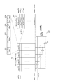
- FIG. 1 is a diagram illustrating an example of an overall configuration of an information processing system according to an embodiment of the present technology.
- FIG. 2 is a diagram illustrating an example of a configuration of a storage controller 200 according to the embodiment of the present technology.
- FIG. 3 is a diagram illustrating an example of a configuration of a cache management table 210 and a cache address comparison unit 220 according to the embodiment of the present technology.
- FIG. 9 is a diagram illustrating an example of a configuration of a candidate cache management table 270 and a candidate cache address comparison unit 280 according to the embodiment of the present technology.
- FIG. 7 is a diagram illustrating an example of a relationship between a cache storage 400 and a candidate cache and an access frequency according to the embodiment of the present technology.
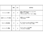
- FIG. 7 is a diagram illustrating an example of a set value in a cache replacement algorithm according to an embodiment of the present technology.
- FIG. 9 is a diagram illustrating an example of a threshold value in a cache replacement algorithm according to an embodiment of the present technology.
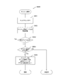
- 14 is a flowchart illustrating an example of a processing procedure of an access operation of the storage controller 200 according to the embodiment of the present technology.
- 15 is a flowchart illustrating an example of a processing procedure of a cache update process of a cache management table update unit 250 according to the embodiment of the present technology.
- 15 is a flowchart illustrating an example of a processing procedure of a write-back determination process of a cache management table updating unit according to an embodiment of the present technology.
- 15 is a flowchart illustrating an example of a processing procedure of a candidate cache update process of a candidate cache management table update unit 290 according to the embodiment of the present technology. 15 is a flowchart illustrating an example of a processing procedure of cache registration processing of a cache management table updating unit 250 according to the embodiment of the present technology.
- FIG. 1 is a diagram illustrating an example of an overall configuration of an information processing system according to an embodiment of the present technology.
- This information processing system includes a host computer 100, a storage controller 200, a main storage 300, and a cache storage 400.
- the storage controller 200, the main storage 300, and the cache storage 400 constitute a storage device 500.
- the host computer 100 issues a command to the storage system to request data read processing, write processing, and the like.
- the host computer 100 has a function of transmitting, to the storage controller 200, a command for instructing the operation of the storage controller 200 and an address indicating an operation target of the command via the signal line 102.
- the host computer 100 has a function of transmitting and receiving data to and from the storage controller via a signal line (not shown).
- the storage controller 200 receives a command by communicating with the host computer 100, and requests the main storage 300 or the cache storage 400 to perform a read process or a write process.
- the storage controller 200 transmits a request for instructing the operation of the main storage 300 and an address indicating an operation target of the request to the main storage 300 via a signal line 203. Further, the storage controller 200 transmits a request for instructing the operation of the cache storage 400 and an address indicating an operation target of the request to the cache storage 400 via the signal line 204.
- the storage controller 200 transmits and receives data to and from the main storage 300 or the cache storage 400 via a signal line (not shown).
- the main storage 300 is a storage that stores all data as the storage device 500.
- the main storage 300 is a storage device having a larger capacity and a slower response speed than the cache storage 400.
- a non-volatile memory such as a hard disk or a NAND flash memory is assumed.
- the main storage 300 reads or writes data according to a request received from the storage controller 200 via the signal line 203.
- the cache storage 400 is a storage that holds frequently accessed data.
- the cache storage 400 is a storage device having a smaller capacity and a faster response speed than the main storage 300, and operates as a cache of the main storage 300. That is, a part of the data of the main storage 300 is stored in the cache storage 400.
- As the cache storage 400 for example, a high-speed nonvolatile memory such as a resistance change type memory is assumed. In a non-volatile memory, the number of times of writing often has an upper limit. However, by selecting data that is expected to have a cache hit and registering the data in the cache storage 400 according to this embodiment, the number of times of writing in the cache storage 400 can be reduced. Life can be extended.
- the cache storage 400 reads or writes data according to a request received from the storage controller 200 via the signal line 204.
- the access frequency is checked, and only data with a high access frequency is registered in the cache storage 400.
- a candidate cache is introduced and the access frequency is measured. This candidate cache stores candidate entries for storing address information and access frequency without storing data.
- FIG. 2 is a diagram illustrating an example of a configuration of the storage controller 200 according to the embodiment of the present technology.
- the storage controller 200 includes a cache management table 210, a cache address comparison unit 220, a main storage control unit 230, a cache storage control unit 240, a cache management table update unit 250, a cache data update unit 260, a candidate cache It includes a management table 270, a candidate cache address comparison unit 280, and a candidate cache management table update unit 290.
- the cache management table 210 is a table that holds cache entries for managing the cache storage 400.
- the cache management table 210 is an example of a cache management unit described in the claims.
- the cache address comparison unit 220 compares the address specified by the host computer 100 with the address of the cache entry in the cache management table 210 to determine a cache hit or a mishit.
- the main storage control unit 230 accesses the main storage 300 based on the address specified by the host computer 100 when the result of the determination by the cache address comparison unit 220 is a cache miss.
- the cache management table updating unit 250 updates the cache management information of the corresponding set on the cache management table 210 based on the determination result of the cache address comparison unit 220.
- the cache storage control unit 240 accesses data in the cache storage 400 based on the cache address output from the cache management table updating unit 250.
- the cache data updating unit 260 performs data transfer between the main storage 300 and the cache storage 400 based on an instruction from the cache management table updating unit 250.
- the candidate cache management table 270 is a table that holds candidate entries of the candidate cache before being registered in the cache storage 400.
- the candidate cache management table 270 is an example of a candidate cache management unit described in the claims.
- the candidate cache address comparison unit 280 compares the address specified by the host computer 100 with the address registered in the candidate cache management information (candidate entry) of the candidate cache management table 270, and determines whether or not the address has been registered in the candidate cache. Is determined.
- the candidate cache management table updating unit 290 updates the candidate cache management information of the corresponding set on the candidate cache management table 270 based on the determination result by the candidate cache address comparison unit 280.
- the candidate cache management table update unit 290 determines whether or not to register the candidate entry in the cache management table 210 with reference to the access frequency held in the candidate cache management information. Based on the result of the determination by the candidate cache management table update unit 290, the cache management table update unit 250 registers new address information in the cache management table 210.
- the cache management table update unit 250, the candidate cache management table update unit 290, and the cache data update unit 260 are examples of the cache update unit described in the claims.
- FIG. 3 is a diagram illustrating an example of a configuration of the cache management table 210 and the cache address comparison unit 220 according to the embodiment of the present technology.
- a 4-way set associative memory is assumed as the configuration of the cache storage 400. Then, the total capacity of the cache storage 400 is set to 64 MB, and the cache storage 400 is managed by 4 KB pages. The cache storage 400 is accessed using a part of the address as a set address. In this example, each set holds up to four cache entries. That is, since there are four ways per set, the cache storage 400 has a total of 4096 sets.
- the set has 2048 pages. That is, up to four pages out of the 2048 pages are held in the cache storage 400.
- the cache management information of the cache entry stored corresponding to each way in the cache management table 210 includes, for example, a 1-bit valid flag 211, 20-bit address information 212, 8-bit access frequency information 213, and 1-bit access frequency information 213. And a bit dirty flag 214.
- the valid flag 211 is a flag indicating whether or not the cache entry is valid (valid). For example, if the valid flag 211 indicates “1”, it indicates that the cache entry is “valid”, and if it indicates “0”, it indicates that the cache entry is “invalid”.
- the address information 212 holds an address portion (associative address) corresponding to the cache entry.
- the address information 212 is referred to by the cache address comparing unit 220 and is compared with the address part of the address specified by the host computer 100.
- the access frequency information 213 holds a value indicating the access frequency of the cache entry. This value is referred to when replacing the cache entry. For example, when the value of the access frequency information 213 falls below the cache-out threshold, the cache entry becomes a deletion candidate (scheduled to be deleted) from the cache management table 210.
- the dirty flag 214 is a flag indicating whether data in the cache entry matches the data in the main storage 300. For example, if the dirty flag 214 indicates “1”, it indicates that there is no match (dirty), and if it indicates “0”, it indicates that they match. In order to maintain consistency (coherency) between the main storage 300 and the cache storage 400, it is necessary to write back the data of the cache entry in a mismatched state from the cache storage 400 to the main storage 300. The write-back timing will be described later.
- the cache address comparing unit 220 includes four comparators 221 and a hit determining unit 222.
- the comparator 221 compares the four pieces of address information 212 read from the cache management table 210 according to the set address of the address specified by the host computer 100, and the associative address that is a part of the address specified by the host computer 100. Compare. When a match is detected in any of the four comparators 221, the hit determination unit 222 outputs a determination result indicating a cache hit. On the other hand, if no match is detected in any of the four comparators 221, a determination result indicating a cache miss is output. This determination result is supplied to the cache storage control unit 240 and the cache management table updating unit 250.
- the cache address comparison unit 220 compares only cache entries whose valid flag 211 is “valid”, and the cache entry whose valid flag 211 indicates “invalid” has one address. Even if it does, it is not determined as a cache hit.
- FIG. 4 is a diagram illustrating an example of a configuration of the candidate cache management table 270 and the candidate cache address comparison unit 280 according to the embodiment of the present technology.
- the candidate cache management table 270 holds eight sets of candidate cache management information (candidate entries) per set.
- the candidate cache management information of the candidate entry stored corresponding to each way of the candidate cache management table 270 includes, for example, a 1-bit valid flag 271, 20-bit address information 272, 8-bit access frequency information 273, Is provided. These are the same as the cache management information in the cache management table 210 described above, but do not have a dirty flag because there is no data storage area.
- the candidate cache address comparison unit 280 includes eight comparators 281 and a hit determination unit 282. These are the same as the above-described cache address comparison unit 220.
- the hit determination unit 282 When a match is detected in any of the eight comparators 281, the hit determination unit 282 outputs a determination result indicating that the hit has been registered in the candidate cache. On the other hand, if no match is detected in any of the eight comparators 281, a determination result indicating that they are not registered in the candidate cache is output.
- the candidate entry is newly registered in the cache entry of the cache management table 210.
- a cache entry whose valid flag 211 indicates “invalid” or a cache entry to be deleted is used. Further, the cache entry registered in the cache management table 210 is deleted from the candidate cache. That is, the valid flag 271 is set to “invalid”.
- the candidate entry is not registered in the cache management table 210, and It becomes a deletion candidate (to be deleted).
- FIG. 5 is a diagram illustrating an example of the relationship between the cache storage 400 and the candidate cache and the access frequency according to the embodiment of the present technology.
- FIG. 6 is a diagram illustrating an example of a set value in the cache replacement algorithm according to the embodiment of the present technology.
- FIG. 7 is a diagram illustrating an example of a threshold value in the cache replacement algorithm according to the embodiment of the present technology.
- the access frequency of the address specified in the command issued from the host computer 100 is monitored without immediately registering it in the cache storage 400. For this purpose, it is initially registered in the candidate cache management table 270 of the candidate cache. At this time, for example, a candidate cache initial value “32” is set as the initial value of the access frequency information 273.
- the value of the access frequency information 273 After being registered in the candidate cache management table 270, the value of the access frequency information 273 increases each time there is an access that matches the candidate entry. For example, a cache hit addition value “4” is added. On the other hand, the value of the access frequency information 273 decreases each time there is an access that does not match the candidate entry. For example, the subtraction value “1” at the time of a cache miss is subtracted.
- the candidate entry is registered as a cache entry in the cache management table 210. In that case, the candidate entry is deleted from the candidate cache management table 270.
- the value of the access frequency information 273 is inherited as it is as the access frequency information 213.
- the cache-in threshold is set to, for example, "40".
- the candidate entry becomes a deletion candidate (to be deleted) from the candidate cache management table 270.
- the candidate cashout threshold is, for example, "16".
- the value of the access frequency information 213 increases each time there is an access that matches the cache entry. For example, “4” is added.
- the value of the access frequency information 213 decreases each time there is an access that does not match the cache entry. For example, “1” is subtracted.
- the candidate entry becomes a deletion candidate (to be deleted) from the cache management table 210.
- the information may be deleted immediately from the cache management table 210, but there is no problem if it remains valid until another registered item is generated.
- the cashout threshold is, for example, “8”.
- the data of the cache entry in a mismatched state is written back from the cache storage 400 to the main storage 300 at a timing below the write-back start threshold. This makes it possible to prepare for deletion from the cache management table 210 in advance.
- the write-back start threshold is, for example, "16".
- the numerical values of the set values and the threshold values shown in this embodiment are merely examples, and it goes without saying that appropriate values may be used as appropriate.
- the numerical example is given so that the value of the access frequency information is increased when the access frequency is high, the value of the access frequency information may be increased when the access frequency is low.
- the magnitude relationship with the threshold is also reversed.
- FIG. 8 is a flowchart illustrating an example of a processing procedure of an access operation of the storage controller 200 according to the embodiment of the present technology.
- the cache management table 210 is referred to in the storage controller 200, and the cache update processing is performed by the cache management table update unit 250 (step S910). If there is a cache hit (step S921: Yes), the cache address is output to the cache storage control unit 240 (step S922). Thereby, the cache storage 400 is accessed (step S923). Then, the updating process is also performed on the candidate cache (step S801).
- step S921 if there is a cache miss (step S921: No), the input address is output to the main storage control unit 230 (step S924). Thereby, the main storage 300 is accessed (step S925). Then, the update process is also performed on the candidate cache (step S802). As a result, when registration from the candidate cache to the cache storage 400 occurs (step S926: Yes), data copy processing is performed as follows. That is, the input address is output to the main storage control unit 230 (step S927), and the cache address is output to the cache storage control unit 240 (step S928). Then, the data is copied from the main storage 300 to the cache storage 400 (Step S929).
- step S930 it is determined whether or not it is necessary to perform write-back in the cache storage 400 (step S930).
- step S941: Yes the following write-back processing is performed. That is, the cache address is output to the cache storage control unit 240 (Step S942), and the input address is output to the main storage control unit 230 (Step S943). Then, the data is copied from the cache storage 400 to the main storage 300 (Step S944).
- FIG. 9 is a flowchart illustrating an example of a processing procedure of a cache update process (step S910) of the cache management table update unit 250 according to the embodiment of the present technology.
- a set address is calculated from the address issued from the host computer 100 (step S911). Then, the cache management information of the cache management table 210 is referred to by the set address (step S912).
- the set address In this example, a 4-way set associative memory is assumed as the cache storage 400, so that cache management information of four cache entries is obtained.
- step S913 If there is a way that matches the address issued from the host computer 100 among the four pieces of acquired cache management information (step S913: Yes), “4” is added to the value of the access frequency information 213 of the matched way. (Step S915). This “4” is an example of the above-described cache hit addition value. Then, “1” is subtracted from the value of the access frequency information 213 of the three ways other than the matched way (step S916). This “1” is an example of the above-described subtraction value at the time of a cache miss. At the time of the subtraction, if the access frequency information 213 is already “0”, the subtraction is unnecessary. The update of the access frequency information 213 is unnecessary for the cache management information for which the valid flag 211 indicates “invalid”.
- step S913 if there is no way that matches the address issued from the host computer 100 (step S913: No), “1” of the cache miss subtraction value is subtracted from the values of the access frequency information 213 of the four cache management information ( Step S914). At the time of the subtraction, if the access frequency information 213 is already “0”, the subtraction is unnecessary. The update of the access frequency information 213 is unnecessary for the cache management information for which the valid flag 211 indicates “invalid”.
- step S913: Yes If there is a way that matches the address issued from the host computer 100 (step S913: Yes), it is a cache hit, and if there is no matching way (step S913: No), it is a mishit.
- Each result is reported to the cache storage control unit 240 and the cache management table updating unit 250.
- FIG. 10 is a flowchart illustrating an example of a processing procedure of the write-back determination processing (step S930) of the cache management table updating unit 250 according to the embodiment of the present technology.
- step S931 the cache management information in the cache management table 210 is referred to (step S931). Then, it is determined whether or not any of the access frequency information 213 of the four pieces of cache management information has a way below the write-back start threshold (step S932).
- step S932 If there is a way below the write-back start threshold (step S932: Yes) and the dirty flag 214 of that way indicates “mismatch” (dirty) (step S933: Yes), it is determined that write-back has occurred. judge. On the other hand, if there is no way below the write-back start threshold (step S932: No), or if there is a way below the write-back start threshold, the dirty flag 214 of that way indicates "match” (step S932). S933: No), it is determined that write back does not occur.
- FIG. 11 is a flowchart illustrating a processing procedure example of the candidate cache update processing (steps S801 and S802) of the candidate cache management table update unit 290 according to the embodiment of the present technology.
- the set address is calculated from the address issued from the host computer 100 (step S811). Then, the candidate cache management information of the candidate cache management table 270 is referred to by the set address (step S812). In this example, since an 8-way set associative memory is assumed as the candidate cache, candidate cache management information of eight candidate entries is obtained.
- step S813 If there is a way that matches the address issued from the host computer 100 among the obtained eight pieces of candidate cache management information (step S813: YES), the value of the access frequency information 273 of the matching way is added to the value of the cache hit. Is added (step S814).
- step S815: Yes when the value of the access frequency information 273 exceeds the cache-in threshold (step S815: Yes), the candidate entry is registered in the cache management table 210 (step S950).
- Step S816: Yes the original candidate entry is deleted from the candidate cache management table 270 (Step S817). That is, the valid flag 271 is cleared to "invalid".
- the cache miss subtraction value “1” is subtracted from the value of the access frequency information 273 of the seven ways other than the matched way (step S818). At the time of the subtraction, if the access frequency information 273 is already “0”, the subtraction is unnecessary. The update of the access frequency information 273 is unnecessary for the cache management information in which the valid flag 271 indicates “invalid”.
- step S813 if there is no way that matches the address issued from the host computer 100 (step S813: No), an attempt is made to register the candidate cache. At this time, if there is a way in which the validity flag 271 indicates “invalid” in the eight candidate cache management information (step S821: Yes), new registration is performed for that way (step S822). At this time, in the candidate cache management information, the input address is set in the address information 272, the candidate cache initial value “32” is set in the access frequency information 273, and the valid flag 271 is set to “valid”. .
- step S821 If there is no way in which the valid flag 271 indicates "invalid” in the eight candidate cache management information (step S821: No), if there is a way in which the access frequency information 273 indicates "0" (step S823: Yes) ), A new registration is made for the way (step S824). At that time, in the candidate cache management information, the input address is set in the address information 272, and the candidate cache initial value “32” is set in the access frequency information 273, for example.
- step S821: No If there is no way in the eight candidate cache management information indicating that the valid flag 271 indicates “invalid” (step S821: No) and there is no way indicating that the access frequency information 273 indicates “0” (step S823: No), the candidate It does not register in the cache.
- step S813: No if there is no way that matches the address issued from the host computer 100 (step S813: No), if the value of the access frequency information 273 does not exceed the cache-in threshold (step S815: No), the cache registration is completed If not (step S816: No), “1” of the cache miss subtraction value is subtracted from the value of the access frequency information 273 of each way (step S828). At the time of the subtraction, if the access frequency information 273 is already “0”, the subtraction is unnecessary. The update of the access frequency information 273 is unnecessary for the cache management information in which the valid flag 271 indicates “invalid”.
- FIG. 12 is a flowchart illustrating an example of a processing procedure of cache registration processing (step S950) of the cache management table update unit 250 according to the embodiment of the present technology.
- the set address is calculated from the address issued from the host computer 100 (step S951). Then, the cache management information of the cache management table 210 is referred to by the set address (step S952).
- the set address In this example, a 4-way set associative memory is assumed as the cache storage 400, so that cache management information of four cache entries is obtained.
- step S953 If there is a way in which the valid flag 211 indicates “invalid” among the four pieces of acquired cache management information (step S953: Yes), the way is registered in the way (step S955). At this time, the input address is set in the address information 212, and the value of the access frequency information 273 of the candidate cache is copied into the access frequency information 213.
- step S953: No If there is no way for which the validity flag 211 indicates "invalid” (step S953: No), and if there is a way for which the access frequency information 213 indicates "0" (step S954: Yes), registration is performed for that way (step S954). S955). If there is no way indicating that the access frequency information 213 indicates “0” (step S954: No), registration in the cache management table 210 is not performed.
- the access frequency is monitored using the candidate cache management table 270, and when the data exceeds the cache-in threshold, the cache storage 400 register. As a result, only data for which a cache hit can be expected can be registered in the cache storage 400.
- the processing procedure described in the above-described embodiment may be regarded as a method having a series of these procedures, and may be a program for causing a computer to execute the series of procedures or a recording medium storing the program. May be caught.
- a recording medium for example, a CD (Compact Disc), an MD (MiniDisc), a DVD (Digital Versatile Disc), a memory card, a Blu-ray Disc (Blu-ray (registered trademark) Disc), or the like can be used.
- the present technology may have the following configurations.
- a cache management unit that holds an access frequency for each cache entry of a cache storage that stores a part of data stored in a main storage;
- a candidate cache management unit that holds the access frequency for each candidate entry that is not registered in the cache storage;
- a storage control device comprising: a cache update unit that updates the access frequency according to an address of an issued access command, and updates the cache entry and the candidate entry based on the access frequency.
- the cache update unit registers the address in the candidate entry, and The storage control device according to (1), wherein an initial value is set for the access frequency of the entry.
- the cache update unit When the access frequency of the candidate entry is higher than a predetermined cache-in threshold, the cache update unit causes the candidate entry to be registered as the cache entry of the cache storage, and the corresponding data of the main storage to be registered.
- the storage control device according to the above (1) or (2), wherein the storage control device stores the data in the cache storage.
- the cache update unit deletes the original candidate entry when registering the candidate entry having the access frequency higher than the cache-in threshold as the cache entry of the cache storage.
- the storage control device according to (1).
- the cache update unit sets the cache entry as a deletion candidate from the cache storage.
- a storage control device according to any one of claims 1 to 3.
- the cache update unit When the access frequency of the cache entry becomes lower than a predetermined write-back start threshold, the cache update unit, if the data in the cache storage of the cache entry does not match the main storage, deletes the data.
- the storage control device according to any one of (1) to (5), wherein the data is transferred from the cache storage to the main storage.
- the cache updating unit according to any one of (1) to (6), wherein when the access frequency of the candidate entry becomes lower than a predetermined candidate cache-out threshold, the cache update unit sets the candidate entry as a deletion candidate. Storage controller.
- the cache update unit increases the value of the access frequency of the entry.
- main storage A cache storage for storing a part of data stored in the main storage; A cache management unit that holds an access frequency for each cache entry of the cache storage; A candidate cache management unit that holds the access frequency for each candidate entry that is not registered in the cache storage; A storage device comprising: a cache update unit that updates the access frequency according to an address of an issued access command, and updates the cache entry and the candidate entry based on the access frequency.
- the cache storage is a nonvolatile memory having an upper limit on the number of times of writing.
- (11) a host computer; Main storage, A cache storage for storing a part of data stored in the main storage; A cache management unit that holds an access frequency for each cache entry of the cache storage; A candidate cache management unit that holds the access frequency for each candidate entry that is not registered in the cache storage; An information processing system comprising: a cache update unit that updates the access frequency according to an address of an access command issued by the host computer, and updates the cache entry and the candidate entry based on the access frequency.
- REFERENCE SIGNS LIST 100 host computer 200 storage controller 210 cache management table 211 valid flag 212 address information 213 access frequency information 214 dirty flag 220 cache address comparison unit 221 comparator 222 hit determination unit 230 main storage control unit 240 cache storage control unit 250 cache management table update Unit 260 cache data update unit 270 candidate cache management table 271 valid flag 272 address information 273 access frequency information 280 candidate cache address comparison unit 281 comparator 282 hit determination unit 290 candidate cache management table update unit 300 main storage 400 cache storage 500 storage device
Landscapes
- Engineering & Computer Science (AREA)
- Theoretical Computer Science (AREA)
- Physics & Mathematics (AREA)
- General Engineering & Computer Science (AREA)
- General Physics & Mathematics (AREA)
- Human Computer Interaction (AREA)
- Memory System Of A Hierarchy Structure (AREA)
Abstract
アクセス頻度が高いデータのみをキャッシュストレージに登録する。 キャッシュストレージは、メインストレージに記憶されるデータの一部を記憶する。キャッシュ管理部は、キャッシュストレージのキャッシュエントリ毎に、アクセス頻度を保持する。候補キャッシュ管理部は、キャッシュストレージに登録されていない候補エントリ毎に、アクセス頻度を保持する。キャッシュ更新部は、発行されたアクセスコマンドのアドレスに応じてアクセス頻度を更新して、アクセス頻度に基づいてキャッシュエントリおよび前記候補エントリを更新する。
Description
本技術は、記憶制御装置に関する。詳しくは、キャッシュストレージを制御する記憶制御装置、および、その記憶制御装置を含む記憶装置および情報処理システムに関する。
キャッシュメモリ(キャッシュストレージ)のキャッシュエントリを管理するために、最も長く参照されていないキャッシュエントリをリプレース対象とするLRU(Least Recently Used)方式が知られている。このLRU方式では、キャッシュメモリの直近の参照順序のみを考慮しているため、アクセス頻度の高いデータであってもリプレース対象にされるおそれがある。そのため、アクセス頻度を考慮したキャッシュメモリの制御方法が提案されている。例えば、あるウェイに連続してアクセスがあった場合にそのウェイのアクセス頻度ビットをセットして、それ以外のウェイをリプレースするように制御するキャッシュメモリ制御装置が提案されている(例えば、特許文献1参照。)。
上述の従来技術では、キャッシュメモリに残すべきデータを決定しており、キャッシュメモリに新たに登録されるデータとしては、最も直近にアクセスの発生したデータが選択される。しかしながら、新たに登録されたデータがキャッシュヒットするか否かは不明であり、もしキャッシュヒットが期待できないデータをキャッシュメモリに登録してしまうと、メモリとキャッシュメモリとの間で煩雑なデータの移動が生じることになる。そして、これにより、ホストコンピュータからのキャッシュメモリへのアクセスを妨げてしまい、アクセス低下の要因となり得る。また、キャッシュメモリとして不揮発性メモリを使用した場合、書込み回数に上限を有するため、煩雑なデータの移動が繰り返されると、書込み回数が増加して、寿命を短くしてしまうおそれがある。
本技術はこのような状況に鑑みて生み出されたものであり、キャッシュストレージに登録する前にアクセス頻度を確認し、アクセス頻度が高いデータのみをキャッシュストレージに登録することを目的とする。
本技術は、上述の問題点を解消するためになされたものであり、その第1の側面は、メインストレージに記憶されるデータの一部を記憶するキャッシュストレージのキャッシュエントリ毎にアクセス頻度を保持するキャッシュ管理部と、上記キャッシュストレージに登録されていない候補エントリ毎に上記アクセス頻度を保持する候補キャッシュ管理部と、発行されたアクセスコマンドのアドレスに応じて上記アクセス頻度を更新して、上記アクセス頻度に基づいて上記キャッシュエントリおよび上記候補エントリを更新するキャッシュ更新部とを具備する記憶制御装置、記憶装置および情報処理システムである。これにより、アクセス頻度に基づいてキャッシュストレージのキャッシュエントリおよび候補キャッシュの候補エントリを更新するという作用をもたらす。
また、この第1の側面において、上記キャッシュ更新部は、上記発行されたアクセスコマンドのアドレスが上記キャッシュエントリおよび上記候補エントリの何れにも登録されていない場合には、そのアドレスを上記候補エントリに登録して、その候補エントリの上記アクセス頻度に初期値を設定するようにしてもよい。これにより、アクセスコマンドのアドレスが未登録の場合には、まず候補エントリに登録するという作用をもたらす。
また、この第1の側面において、上記キャッシュ更新部は、上記候補エントリの上記アクセス頻度が所定のキャッシュイン閾値よりも高くなると、上記候補エントリを上記キャッシュストレージの上記キャッシュエントリとして登録させて、上記メインストレージの対応するデータを上記キャッシュストレージに記憶させるようにしてもよい。これにより、アクセス頻度がキャッシュイン閾値よりも高くなった際に、データをキャッシュストレージに記憶させるという作用をもたらす。
また、この場合において、上記キャッシュ更新部は、上記アクセス頻度が上記キャッシュイン閾値よりも高くなった上記候補エントリを上記キャッシュストレージの上記キャッシュエントリとして登録させる際に、元の上記候補エントリを削除するようにしてもよい。
また、この第1の側面において、上記キャッシュ更新部は、上記キャッシュエントリの上記アクセス頻度が所定のキャッシュアウト閾値よりも低くなると、そのキャッシュエントリを上記キャッシュストレージからの削除候補とするようにしてもよい。これにより、アクセス頻度がキャッシュアウト閾値よりも低くなった際に、キャッシュストレージからの削除予定とするという作用をもたらす。
また、この第1の側面において、上記キャッシュ更新部は、上記キャッシュエントリの上記アクセス頻度が所定のライトバック開始閾値よりも低くなると、そのキャッシュエントリの上記キャッシュストレージにおけるデータが上記メインストレージと不一致であれば、そのデータを上記キャッシュストレージから上記メインストレージに転送するようにしてもよい。これにより、キャッシュストレージから削除される前の段階において、ライトバック開始閾値よりも低くなった際に、キャッシュストレージへのライトバックを行うという作用をもたらす。
また、この第1の側面において、上記キャッシュ更新部は、上記候補エントリの上記アクセス頻度が所定の候補キャッシュアウト閾値よりも低くなると、その候補エントリを削除候補とするようにしてもよい。これにより、アクセス頻度が所定の候補キャッシュアウト閾値よりも低くなった際に、候補キャッシュからの削除予定とするという作用をもたらす。
また、この第1の側面において、上記キャッシュ更新部は、上記発行されたアクセスコマンドのアドレスが上記キャッシュエントリまたは上記候補エントリの何れかに登録されている場合には、そのエントリの上記アクセス頻度の値をより高くして、それ以外のエントリの上記アクセス頻度の値をより低くするようにしてもよい。これにより、キャッシュストレージまたは候補キャッシュにおけるキャッシュヒットの状態に応じてアクセス頻度の値を更新するという作用をもたらす。
また、この第1の側面において、上記キャッシュストレージは、書込み回数に上限を有する不揮発性メモリであってもよい。この場合、キャッシュストレージにおけるキャッシュヒットが期待されるデータを選んで登録することにより、書込み回数を減らして、寿命を延ばすという作用をもたらす。
本技術によれば、アクセス頻度が高いデータのみをキャッシュストレージに登録することができるという優れた効果を奏し得る。なお、ここに記載された効果は必ずしも限定されるものではなく、本開示中に記載されたいずれかの効果であってもよい。
以下、本技術を実施するための形態(以下、実施の形態と称する)について説明する。説明は以下の順序により行う。
1.ハードウェア構成
2.キャッシュリプレースアルゴリズム
3.動作
1.ハードウェア構成
2.キャッシュリプレースアルゴリズム
3.動作
<1.ハードウェア構成>
[情報処理システム]
図1は、本技術の実施の形態における情報処理システムの全体構成の一例を示す図である。この情報処理システムは、ホストコンピュータ100と、ストレージコントローラ200と、メインストレージ300と、キャッシュストレージ400とから構成される。ストレージコントローラ200、メインストレージ300およびキャッシュストレージ400は、記憶装置500を構成する。
[情報処理システム]
図1は、本技術の実施の形態における情報処理システムの全体構成の一例を示す図である。この情報処理システムは、ホストコンピュータ100と、ストレージコントローラ200と、メインストレージ300と、キャッシュストレージ400とから構成される。ストレージコントローラ200、メインストレージ300およびキャッシュストレージ400は、記憶装置500を構成する。
ホストコンピュータ100は、ストレージシステムに対してデータのリード処理やライト処理等を要求するコマンドを発行するものである。このホストコンピュータ100は、信号線102により、ストレージコントローラ200の動作を指示するコマンドとそのコマンドの操作対象を示すアドレスとをストレージコントローラ200に送信する機能を有する。また、このホストコンピュータ100は、図示しない信号線により、ストレージコントローラとの間のデータ送受信を行う機能を有する。
ストレージコントローラ200は、ホストコンピュータ100と通信してコマンドを受信し、メインストレージ300またはキャッシュストレージ400に対してリード処理またはライト処理を要求するものである。このストレージコントローラ200は、信号線203により、メインストレージ300の動作を指示するリクエストとそのリクエストの操作対象を示すアドレスとをメインストレージ300に送信する。また、このストレージコントローラ200は、信号線204により、キャッシュストレージ400の動作を指示するリクエストとそのリクエストの操作対象を示すアドレスとをキャッシュストレージ400に送信する。また、このストレージコントローラ200は、図示しない信号線により、メインストレージ300またはキャッシュストレージ400とのデータ送受信を行う。
メインストレージ300は、記憶装置500としての全てのデータを記憶するストレージである。このメインストレージ300は、キャッシュストレージ400より大容量かつ応答速度が遅い記憶装置であり、例えば、ハードディスクや、NAND型フラッシュメモリ等の不揮発性メモリが想定される。このメインストレージ300は、ストレージコントローラ200から信号線203を介して受けたリクエストに従ってデータの読出しまたは書込みを行う。
キャッシュストレージ400は、アクセス頻度の高いデータを保持するストレージである。このキャッシュストレージ400は、メインストレージ300より小容量かつ応答速度が速い記憶装置であり、メインストレージ300のキャッシュとして動作する。すなわち、このキャッシュストレージ400には、メインストレージ300のデータの一部が格納される。このキャッシュストレージ400としては、例えば、抵抗変化型メモリ等の高速な不揮発性メモリが想定される。不揮発性メモリにおいては書込み回数に上限を有することが多いが、この実施の形態によりキャッシュヒットが期待されるデータを選んでキャッシュストレージ400に登録することにより、キャッシュストレージ400の書込み回数を減らして、寿命を延ばすことができる。このキャッシュストレージ400は、ストレージコントローラ200から信号線204を介して受けたリクエストに従ってデータの読出しまたは書込みを行う。
このようなシステム構成において、キャッシュストレージ400にデータを登録する前に、アクセス頻度を確認し、アクセス頻度が高いデータのみをキャッシュストレージ400に登録する。そのために、候補キャッシュを導入し、アクセス頻度を計測する。この候補キャッシュは、データを記憶せずに、アドレス情報やアクセス頻度を記憶する候補エントリを記憶する。
[ストレージコントローラ]
図2は、本技術の実施の形態におけるストレージコントローラ200の構成の一例を示す図である。
図2は、本技術の実施の形態におけるストレージコントローラ200の構成の一例を示す図である。
このストレージコントローラ200は、キャッシュ管理テーブル210と、キャッシュアドレス比較部220と、メインストレージ制御部230と、キャッシュストレージ制御部240と、キャッシュ管理テーブル更新部250と、キャッシュデータ更新部260と、候補キャッシュ管理テーブル270と、候補キャッシュアドレス比較部280と、候補キャッシュ管理テーブル更新部290とを備える。
キャッシュ管理テーブル210は、キャッシュストレージ400を管理するためのキャッシュエントリを保持するテーブルである。なお、キャッシュ管理テーブル210は、特許請求の範囲に記載のキャッシュ管理部の一例である。
キャッシュアドレス比較部220は、ホストコンピュータ100から指定されたアドレスと、キャッシュ管理テーブル210のキャッシュエントリのアドレスとを比較して、キャッシュヒットまたはミスヒットの判定を行うものである。
メインストレージ制御部230は、キャッシュアドレス比較部220における判定結果がキャッシュミスであった場合に、ホストコンピュータ100から指定されたアドレスに基づいてメインストレージ300にアクセスを行うものである。
キャッシュ管理テーブル更新部250は、キャッシュアドレス比較部220の判定結果に基づいてキャッシュ管理テーブル210上の該当するセットのキャッシュ管理情報を更新するものである。
キャッシュストレージ制御部240は、キャッシュ管理テーブル更新部250が出力するキャッシュアドレスに基づいて、キャッシュストレージ400上のデータにアクセスを行うものである。
キャッシュデータ更新部260は、キャッシュ管理テーブル更新部250からの指示に基づいて、メインストレージ300とキャッシュストレージ400との間でデータ転送を行うものである。
候補キャッシュ管理テーブル270は、キャッシュストレージ400に登録する前の、候補キャッシュの候補エントリを保持するテーブルである。なお、候補キャッシュ管理テーブル270は、特許請求の範囲に記載の候補キャッシュ管理部の一例である。
候補キャッシュアドレス比較部280は、ホストコンピュータ100から指定されたアドレスと、候補キャッシュ管理テーブル270の候補キャッシュ管理情報(候補エントリ)に登録されたアドレスとを比較して、候補キャッシュに登録済か否かの判定を行うものである。
候補キャッシュ管理テーブル更新部290は、候補キャッシュアドレス比較部280による判定結果に基づいて、候補キャッシュ管理テーブル270上の該当するセットの候補キャッシュ管理情報を更新するものである。この候補キャッシュ管理テーブル更新部290は、候補キャッシュ管理情報に保持されるアクセス頻度を参照して、その候補エントリをキャッシュ管理テーブル210に登録するか否かを判定する。この候補キャッシュ管理テーブル更新部290による判定結果に基づいて、キャッシュ管理テーブル更新部250は、新たなアドレス情報をキャッシュ管理テーブル210に登録する。
なお、キャッシュ管理テーブル更新部250、候補キャッシュ管理テーブル更新部290、および、キャッシュデータ更新部260は、特許請求の範囲に記載のキャッシュ更新部の一例である。
図3は、本技術の実施の形態におけるキャッシュ管理テーブル210およびキャッシュアドレス比較部220の構成の一例を示す図である。
この例では、キャッシュストレージ400の構成として4ウェイセットアソシアティブメモリを想定する。そして、キャッシュストレージ400の総容量を64MBとし、4KB毎のページにより管理する。このキャッシュストレージ400は、アドレスの一部をセットアドレスとして、アクセスされる。この例では、各セットには最大4つのキャッシュエントリが保持される。すなわち、1セット(set)当たり4ウェイ(way)であるため、キャッシュストレージ400全体で4096セットとなる。
メインストレージ300の総容量を8GBと想定し、これを4096セットで管理すると、1セット当たり2048ページとなる。すなわち、2048ページのうち最大4つのページがキャッシュストレージ400に保持されることになる。
キャッシュ管理テーブル210の各ウェイに対応して記憶されるキャッシュエントリのキャッシュ管理情報は、例えば、1ビットの有効フラグ211と、20ビットのアドレス情報212と、8ビットのアクセス頻度情報213と、1ビットのダーティフラグ214とを備える。
有効フラグ211は、そのキャッシュエントリが有効(バリッド)か否かを示すフラグである。例えば、有効フラグ211が「1」を示していればキャッシュエントリが「有効」であることを表し、「0」を示していればキャッシュエントリが「無効」であることを表す。
アドレス情報212は、そのキャッシュエントリに対応するアドレス部分(連想アドレス)を保持するものである。このアドレス情報212は、キャッシュアドレス比較部220によって参照され、ホストコンピュータ100から指定されたアドレスのアドレス部分と比較される。
アクセス頻度情報213は、そのキャッシュエントリにおけるアクセス頻度を示す値を保持するものである。キャッシュエントリのリプレースの際には、この値が参照される。例えば、このアクセス頻度情報213の値がキャッシュアウト閾値を下回った場合には、そのキャッシュエントリはキャッシュ管理テーブル210からの削除候補(削除予定)となる。
ダーティフラグ214は、そのキャッシュエントリにおけるデータがメインストレージ300と一致しているか否かを示すフラグである。例えば、ダーティフラグ214が「1」を示していれば不一致(ダーティ)であることを表し、「0」を示していれば一致していることを表す。メインストレージ300とキャッシュストレージ400との一致性(コヒーレンシ)を維持するためには、不一致状態にあるキャッシュエントリのデータをキャッシュストレージ400からメインストレージ300にライトバックする必要がある。このライトバックのタイミングについては後述する。
キャッシュアドレス比較部220は、4つの比較器221と、ヒット判定部222とを備える。比較器221は、ホストコンピュータ100から指定されたアドレスのセットアドレスに従ってキャッシュ管理テーブル210から読み出された4つのアドレス情報212と、ホストコンピュータ100から指定されたアドレスの一部である連想アドレスとを比較する。ヒット判定部222は、4つの比較器221の何れかにおいて一致が検出されると、キャッシュヒットである旨の判定結果を出力する。一方、4つの比較器221の何れにおいても一致が検出されない場合にはキャッシュミスである旨の判定結果を出力する。この判定結果は、キャッシュストレージ制御部240およびキャッシュ管理テーブル更新部250に供給される。なお、キャッシュアドレス比較部220において比較対象となるのは有効フラグ211が「有効」なキャッシュエントリのみであり、有効フラグ211が「無効」であることを示しているキャッシュエントリについては、アドレスが一致してもキャッシュヒットとは判定されない。
図4は、本技術の実施の形態における候補キャッシュ管理テーブル270および候補キャッシュアドレス比較部280の構成の一例を示す図である。
この例では、候補キャッシュの構成として8ウェイセットアソシアティブメモリを想定する。この候補キャッシュは、アクセス頻度を監視するためのものであるため、データの記憶領域は不要である。候補キャッシュ管理テーブル270は、1セット当たり8つの候補キャッシュ管理情報(候補エントリ)を保持する。
候補キャッシュ管理テーブル270の各ウェイに対応して記憶される候補エントリの候補キャッシュ管理情報は、例えば、1ビットの有効フラグ271と、20ビットのアドレス情報272と、8ビットのアクセス頻度情報273とを備える。これらは、上述のキャッシュ管理テーブル210のキャッシュ管理情報と同様であるが、データ記憶領域がないため、ダーティフラグは備えていない。
候補キャッシュアドレス比較部280は、8つの比較器281と、ヒット判定部282とを備える。これらは、上述のキャッシュアドレス比較部220と同様である。ヒット判定部282は、8つの比較器281の何れかにおいて一致が検出されると、候補キャッシュに登録済である旨の判定結果を出力する。一方、8つの比較器281の何れにおいても一致が検出されない場合には、候補キャッシュに登録されていない旨の判定結果を出力する。
候補キャッシュに登録されていないアドレスが発生した場合には、候補キャッシュ管理テーブル270の該当するセットにおける候補エントリに新たに登録される。このとき、有効フラグ271が「無効」を示している候補エントリ、または、削除予定の候補エントリが使用される。
また、候補キャッシュに登録されている間に、アクセス頻度情報273がキャッシュイン閾値を超えた場合には、その候補エントリはキャッシュ管理テーブル210のキャッシュエントリに新たに登録される。このとき、有効フラグ211が「無効」を示しているキャッシュエントリ、または、削除予定のキャッシュエントリが使用される。また、キャッシュ管理テーブル210に登録されたキャッシュエントリについては、候補キャッシュから削除される。すなわち、有効フラグ271が「無効」に設定される。
一方、候補キャッシュに登録されている間に、アクセス頻度情報273が候補キャッシュアウト閾値を超えた場合には、その候補エントリはキャッシュ管理テーブル210に登録されることなく、候補キャッシュ管理テーブル270からの削除候補(削除予定)となる。
<2.キャッシュリプレースアルゴリズム>
[アクセス頻度情報]
図5は、本技術の実施の形態におけるキャッシュストレージ400および候補キャッシュとアクセス頻度との関係例を示す図である。図6は、本技術の実施の形態のキャッシュリプレースアルゴリズムにおける設定値の例を示す図である。図7は、本技術の実施の形態のキャッシュリプレースアルゴリズムにおける閾値の例を示す図である。
[アクセス頻度情報]
図5は、本技術の実施の形態におけるキャッシュストレージ400および候補キャッシュとアクセス頻度との関係例を示す図である。図6は、本技術の実施の形態のキャッシュリプレースアルゴリズムにおける設定値の例を示す図である。図7は、本技術の実施の形態のキャッシュリプレースアルゴリズムにおける閾値の例を示す図である。
この実施の形態においては、ホストコンピュータ100から発行されたコマンドにおいて指定されたアドレスについて、すぐにはキャッシュストレージ400に登録せずに、アクセス頻度を監視する。そのために、最初は候補キャッシュの候補キャッシュ管理テーブル270に登録される。このとき、アクセス頻度情報273の初期値として、例えば候補キャッシュ初期値「32」が設定される。
候補キャッシュ管理テーブル270に登録された後、その候補エントリに合致するアクセスがあるたびにアクセス頻度情報273の値は増加する。例えば、キャッシュヒット時加算値「4」が加算されていく。一方、その候補エントリに合致しないアクセスがあるたびにアクセス頻度情報273の値は減少する。例えば、キャッシュミス時減算値「1」が減算されていく。
その結果、アクセス頻度情報273の値が増加してキャッシュイン閾値を超えると、その候補エントリはキャッシュ管理テーブル210のキャッシュエントリとして登録される。その場合、その候補エントリは候補キャッシュ管理テーブル270から削除される。アクセス頻度情報273の値は、アクセス頻度情報213としてそのまま引き継がれる。なお、このキャッシュイン閾値としては、例えば「40」とする。
一方、アクセス頻度情報273の値が減少して候補キャッシュアウト閾値を下回ると、その候補エントリは候補キャッシュ管理テーブル270からの削除候補(削除予定)となる。候補キャッシュ管理テーブル270から速やかに削除するようにしてもよいが、他に登録されるものが発生するまで有効にしておいても問題はない。なお、この候補キャッシュアウト閾値としては、例えば「16」とする。
キャッシュ管理テーブル210に登録された後も、そのキャッシュエントリに合致するアクセスがあるたびにアクセス頻度情報213の値は増加する。例えば、「4」が加算されていく。一方、そのキャッシュエントリに合致しないアクセスがあるたびにアクセス頻度情報213の値は減少する。例えば、「1」が減算されていく。
その結果、アクセス頻度情報213の値が減少してキャッシュアウト閾値を下回ると、その候補エントリはキャッシュ管理テーブル210からの削除候補(削除予定)となる。キャッシュ管理テーブル210から速やかに削除するようにしてもよいが、他に登録されるものが発生するまで有効にしておいても問題はない。なお、このキャッシュアウト閾値としては、例えば「8」とする。
また、キャッシュアウト閾値を下回る前に、ライトバック開始閾値を下回ったタイミングで、不一致状態にあるキャッシュエントリのデータをキャッシュストレージ400からメインストレージ300にライトバックする。これにより、キャッシュ管理テーブル210から削除する準備を予め行うことができる。なお、このライトバック開始閾値としては、例えば「16」とする。
このように、アクセス頻度に応じてキャッシュストレージ400および候補キャッシュにおけるエントリのリプレースが行われる。
[設定値]
ここで、上述の設定値について考察する。キャッシュストレージ400のヒット率を80%と想定すると、4ウェイセットアソシアティブメモリにおいては、40回のアクセスのうち、1ウェイ当たりの平均ヒット回数は8回である。すなわち、40回のアクセスのうち、8回キャッシュヒット、32回ミスヒットとなる。この場合、候補キャッシュへの登録時の初期値を「32」として、ミスヒットとなるたびに「1」を減算する一方で、キャッシュヒットの時の加算値Nとして、
N=32/8=4
を設定することにより、想定するバランスが得られる。
ここで、上述の設定値について考察する。キャッシュストレージ400のヒット率を80%と想定すると、4ウェイセットアソシアティブメモリにおいては、40回のアクセスのうち、1ウェイ当たりの平均ヒット回数は8回である。すなわち、40回のアクセスのうち、8回キャッシュヒット、32回ミスヒットとなる。この場合、候補キャッシュへの登録時の初期値を「32」として、ミスヒットとなるたびに「1」を減算する一方で、キャッシュヒットの時の加算値Nとして、
N=32/8=4
を設定することにより、想定するバランスが得られる。
なお、この実施の形態において示した設定値および閾値の数値例は、あくまで一例であり、適宜適切な値を用いてよいことはいうまでもない。また、アクセス頻度が高い場合にアクセス頻度情報の値が大きくなるように数値例を示したが、逆にアクセス頻度が低い場合にアクセス頻度情報の値が大きくなるようにしてもよい。ただし、その場合、閾値との大小関係も逆になる。
[アクセス頻度情報]
この実施の形態においては、アクセス頻度情報を新たに保持することになる。上述のように8ビット(1バイト)ずつの容量を想定すると、キャッシュ管理テーブル210においてセット毎に4ウェイ、候補キャッシュ管理テーブル270おいてセット毎に8ウェイであるため、
アクセス頻度情報の総量=4096×(4+8)=48Kバイト
となる。これは、キャッシュ全体のデータ量としては比較的少ないと考えられる。
この実施の形態においては、アクセス頻度情報を新たに保持することになる。上述のように8ビット(1バイト)ずつの容量を想定すると、キャッシュ管理テーブル210においてセット毎に4ウェイ、候補キャッシュ管理テーブル270おいてセット毎に8ウェイであるため、
アクセス頻度情報の総量=4096×(4+8)=48Kバイト
となる。これは、キャッシュ全体のデータ量としては比較的少ないと考えられる。
<3.動作>
[アクセス動作]
図8は、本技術の実施の形態におけるストレージコントローラ200のアクセス動作の処理手順例を示す流れ図である。
[アクセス動作]
図8は、本技術の実施の形態におけるストレージコントローラ200のアクセス動作の処理手順例を示す流れ図である。
ホストコンピュータ100からメモリアクセスコマンドが発行されると、ストレージコントローラ200においてキャッシュ管理テーブル210が参照されて、キャッシュ管理テーブル更新部250によりキャッシュ更新処理が行われる(ステップS910)。キャッシュヒットした場合には(ステップS921:Yes)、キャッシュアドレスがキャッシュストレージ制御部240に出力される(ステップS922)。これにより、キャッシュストレージ400にアクセスが行われる(ステップS923)。そして、候補キャッシュについても更新処理が行われる(ステップS801)。
一方、キャッシュミスヒットした場合には(ステップS921:No)、入力アドレスがメインストレージ制御部230に出力される(ステップS924)。これにより、メインストレージ300にアクセスが行われる(ステップS925)。そして、候補キャッシュについても更新処理が行われる(ステップS802)。その結果、候補キャッシュからキャッシュストレージ400への登録が発生した場合には(ステップS926:Yes)、以下のようにデータのコピー処理が行われる。すなわち、入力アドレスがメインストレージ制御部230に出力され(ステップS927)、キャッシュアドレスがキャッシュストレージ制御部240に出力される(ステップS928)。そして、メインストレージ300からキャッシュストレージ400にデータがコピーされる(ステップS929)。
その後、キャッシュストレージ400においてライトバックを行う必要があるか否かが判定される(ステップS930)。その結果、ライトバックが発生した場合には(ステップS941:Yes)、以下のライトバック処理が行われる。すなわち、キャッシュアドレスがキャッシュストレージ制御部240に出力され(ステップS942)、入力アドレスがメインストレージ制御部230に出力される(ステップS943)。そして、キャッシュストレージ400からメインストレージ300にデータがコピーされる(ステップS944)。
[キャッシュ更新]
図9は、本技術の実施の形態におけるキャッシュ管理テーブル更新部250のキャッシュ更新処理(ステップS910)の処理手順例を示す流れ図である。
図9は、本技術の実施の形態におけるキャッシュ管理テーブル更新部250のキャッシュ更新処理(ステップS910)の処理手順例を示す流れ図である。
まず、ホストコンピュータ100から発行されたアドレスからセットアドレスが算出される(ステップS911)。そして、このセットアドレスによりキャッシュ管理テーブル210のキャッシュ管理情報が参照される(ステップS912)。この例では、キャッシュストレージ400として4ウェイセットアソシアティブメモリを想定しているため、4つのキャッシュエントリのキャッシュ管理情報が取得される。
取得された4つのキャッシュ管理情報のうち、ホストコンピュータ100から発行されたアドレスと一致するウェイがあれば(ステップS913:Yes)、一致したウェイのアクセス頻度情報213の値に「4」を加算する(ステップS915)。この「4」は、上述のキャッシュヒット時加算値の一例である。そして、この一致したウェイ以外の3つのウェイのアクセス頻度情報213の値から「1」を減算する(ステップS916)。この「1」は、上述のキャッシュミス時減算値の一例である。なお、減算の際、アクセス頻度情報213が既に「0」であれば、減算は不要である。また、有効フラグ211が「無効」を示しているキャッシュ管理情報については、アクセス頻度情報213の更新は不要である。
一方、ホストコンピュータ100から発行されたアドレスと一致するウェイがなければ(ステップS913:No)、4つのキャッシュ管理情報のアクセス頻度情報213の値からキャッシュミス時減算値の「1」を減算する(ステップS914)。なお、減算の際、アクセス頻度情報213が既に「0」であれば、減算は不要である。また、有効フラグ211が「無効」を示しているキャッシュ管理情報については、アクセス頻度情報213の更新は不要である。
なお、ホストコンピュータ100から発行されたアドレスと一致するウェイがあれば(ステップS913:Yes)キャッシュヒットであり、一致するウェイがなければ(ステップS913:No)ミスヒットである。それぞれの結果がキャッシュストレージ制御部240およびキャッシュ管理テーブル更新部250に報告される。
[ライトバック判定]
図10は、本技術の実施の形態におけるキャッシュ管理テーブル更新部250のライトバック判定処理(ステップS930)の処理手順例を示す流れ図である。
図10は、本技術の実施の形態におけるキャッシュ管理テーブル更新部250のライトバック判定処理(ステップS930)の処理手順例を示す流れ図である。
キャッシュ更新に伴い、キャッシュ管理テーブル210のキャッシュ管理情報が参照される(ステップS931)。そして、4つのキャッシュ管理情報のアクセス頻度情報213のうち、ライトバック開始閾値を下回るウェイがあるか否かが判断される(ステップS932)。
ライトバック開始閾値を下回るウェイがあり(ステップS932:Yes)、そのウェイのダーティフラグ214が「不一致」(ダーティ)を示している場合には(ステップS933:Yes)、ライトバックが発生したものと判定する。一方、ライトバック開始閾値を下回るウェイがなく(ステップS932:No)、または、ライトバック開始閾値を下回るウェイがあってもそのウェイのダーティフラグ214が「一致」を示している場合には(ステップS933:No)、ライトバックは発生しないものと判定する。
[候補キャッシュ更新]
図11は、本技術の実施の形態における候補キャッシュ管理テーブル更新部290の候補キャッシュ更新処理(ステップS801、S802)の処理手順例を示す流れ図である。
図11は、本技術の実施の形態における候補キャッシュ管理テーブル更新部290の候補キャッシュ更新処理(ステップS801、S802)の処理手順例を示す流れ図である。
まず、ホストコンピュータ100から発行されたアドレスからセットアドレスが算出される(ステップS811)。そして、このセットアドレスにより候補キャッシュ管理テーブル270の候補キャッシュ管理情報が参照される(ステップS812)。この例では、候補キャッシュとして8ウェイセットアソシアティブメモリを想定しているため、8つの候補エントリの候補キャッシュ管理情報が取得される。
取得された8つの候補キャッシュ管理情報のうち、ホストコンピュータ100から発行されたアドレスと一致するウェイがあれば(ステップS813:Yes)、一致したウェイのアクセス頻度情報273の値にキャッシュヒット時加算値の「4」を加算する(ステップS814)。その結果、アクセス頻度情報273の値がキャッシュイン閾値を超えると(ステップS815:Yes)、その候補エントリをキャッシュ管理テーブル210に登録する(ステップS950)。キャッシュ管理テーブル210への登録が完了すると(ステップS816:Yes)、元の候補エントリを候補キャッシュ管理テーブル270から削除する(ステップS817)。すなわち、有効フラグ271を「無効」にクリアする。また、一致したウェイ以外の7つのウェイのアクセス頻度情報273の値からキャッシュミス時減算値の「1」を減算する(ステップS818)。なお、減算の際、アクセス頻度情報273が既に「0」であれば、減算は不要である。また、有効フラグ271が「無効」を示しているキャッシュ管理情報については、アクセス頻度情報273の更新は不要である。
一方、ホストコンピュータ100から発行されたアドレスと一致するウェイがなければ(ステップS813:No)、候補キャッシュへの登録を試みる。このとき、8つの候補キャッシュ管理情報の中に有効フラグ271が「無効」を示すウェイがあれば(ステップS821:Yes)、そのウェイに新たに登録を行う(ステップS822)。その際、その候補キャッシュ管理情報において、アドレス情報272には入力アドレスが設定され、アクセス頻度情報273には例えば候補キャッシュ初期値「32」が設定され、有効フラグ271が「有効」に設定される。
8つの候補キャッシュ管理情報の中に有効フラグ271が「無効」を示すウェイがない場合には(ステップS821:No)、アクセス頻度情報273が「0」を示すウェイがあれば(ステップS823:Yes)、そのウェイに新たに登録を行う(ステップS824)。その際、その候補キャッシュ管理情報において、アドレス情報272には入力アドレスが設定され、アクセス頻度情報273には例えば候補キャッシュ初期値「32」が設定される。
8つの候補キャッシュ管理情報の中に有効フラグ271が「無効」を示すウェイがなく(ステップS821:No)、アクセス頻度情報273が「0」を示すウェイもなければ(ステップS823:No)、候補キャッシュへの登録は行わない。
以上において、ホストコンピュータ100から発行されたアドレスと一致するウェイがない場合(ステップS813:No)、アクセス頻度情報273の値がキャッシュイン閾値を超えない場合(ステップS815:No)、キャッシュ登録が完了しない場合(ステップS816:No)には、各ウェイのアクセス頻度情報273の値からキャッシュミス時減算値の「1」を減算する(ステップS828)。なお、減算の際、アクセス頻度情報273が既に「0」であれば、減算は不要である。また、有効フラグ271が「無効」を示しているキャッシュ管理情報については、アクセス頻度情報273の更新は不要である。
[キャッシュ登録]
図12は、本技術の実施の形態におけるキャッシュ管理テーブル更新部250のキャッシュ登録処理(ステップS950)の処理手順例を示す流れ図である。
図12は、本技術の実施の形態におけるキャッシュ管理テーブル更新部250のキャッシュ登録処理(ステップS950)の処理手順例を示す流れ図である。
まず、ホストコンピュータ100から発行されたアドレスからセットアドレスが算出される(ステップS951)。そして、このセットアドレスによりキャッシュ管理テーブル210のキャッシュ管理情報が参照される(ステップS952)。この例では、キャッシュストレージ400として4ウェイセットアソシアティブメモリを想定しているため、4つのキャッシュエントリのキャッシュ管理情報が取得される。
取得された4つのキャッシュ管理情報のうち、有効フラグ211が「無効」を示すウェイがあれば(ステップS953:Yes)、そのウェイに登録が行われる(ステップS955)。その際、アドレス情報212には入力アドレスが設定され、アクセス頻度情報213には候補キャッシュのアクセス頻度情報273の値がコピーされる。
有効フラグ211が「無効」を示すウェイがない場合(ステップS953:No)、アクセス頻度情報213が「0」を示すウェイがあれば(ステップS954:Yes)、そのウェイに登録が行われる(ステップS955)。アクセス頻度情報213が「0」を示すウェイもなければ(ステップS954:No)、キャッシュ管理テーブル210への登録は行われない。
このように、本技術の実施の形態では、データをキャッシュストレージ400に登録する前に、候補キャッシュ管理テーブル270を用いてアクセス頻度を監視して、キャッシュイン閾値を超えた際にキャッシュストレージ400に登録する。これにより、キャッシュヒットが期待できるデータのみをキャッシュストレージ400に登録することができる。
なお、上述の実施の形態は本技術を具現化するための一例を示したものであり、実施の形態における事項と、特許請求の範囲における発明特定事項とはそれぞれ対応関係を有する。同様に、特許請求の範囲における発明特定事項と、これと同一名称を付した本技術の実施の形態における事項とはそれぞれ対応関係を有する。ただし、本技術は実施の形態に限定されるものではなく、その要旨を逸脱しない範囲において実施の形態に種々の変形を施すことにより具現化することができる。
また、上述の実施の形態において説明した処理手順は、これら一連の手順を有する方法として捉えてもよく、また、これら一連の手順をコンピュータに実行させるためのプログラム乃至そのプログラムを記憶する記録媒体として捉えてもよい。この記録媒体として、例えば、CD(Compact Disc)、MD(MiniDisc)、DVD(Digital Versatile Disc)、メモリカード、ブルーレイディスク(Blu-ray(登録商標)Disc)等を用いることができる。
なお、本明細書に記載された効果はあくまで例示であって、限定されるものではなく、また、他の効果があってもよい。
なお、本技術は以下のような構成もとることができる。
(1)メインストレージに記憶されるデータの一部を記憶するキャッシュストレージのキャッシュエントリ毎にアクセス頻度を保持するキャッシュ管理部と、
前記キャッシュストレージに登録されていない候補エントリ毎に前記アクセス頻度を保持する候補キャッシュ管理部と、
発行されたアクセスコマンドのアドレスに応じて前記アクセス頻度を更新して、前記アクセス頻度に基づいて前記キャッシュエントリおよび前記候補エントリを更新するキャッシュ更新部と
を具備する記憶制御装置。
(2)前記キャッシュ更新部は、前記発行されたアクセスコマンドのアドレスが前記キャッシュエントリおよび前記候補エントリの何れにも登録されていない場合には、そのアドレスを前記候補エントリに登録して、その候補エントリの前記アクセス頻度に初期値を設定する
前記(1)に記載の記憶制御装置。
(3)前記キャッシュ更新部は、前記候補エントリの前記アクセス頻度が所定のキャッシュイン閾値よりも高くなると、前記候補エントリを前記キャッシュストレージの前記キャッシュエントリとして登録させて、前記メインストレージの対応するデータを前記キャッシュストレージに記憶させる
前記(1)または(2)に記載の記憶制御装置。
(4)前記キャッシュ更新部は、前記アクセス頻度が前記キャッシュイン閾値よりも高くなった前記候補エントリを前記キャッシュストレージの前記キャッシュエントリとして登録させる際に、元の前記候補エントリを削除する
前記(3)に記載の記憶制御装置。
(5)前記キャッシュ更新部は、前記キャッシュエントリの前記アクセス頻度が所定のキャッシュアウト閾値よりも低くなると、そのキャッシュエントリを前記キャッシュストレージからの削除候補とする
前記(1)から(4)のいずれかに記載の記憶制御装置。
(6)前記キャッシュ更新部は、前記キャッシュエントリの前記アクセス頻度が所定のライトバック開始閾値よりも低くなると、そのキャッシュエントリの前記キャッシュストレージにおけるデータが前記メインストレージと不一致であれば、そのデータを前記キャッシュストレージから前記メインストレージに転送する
前記(1)から(5)のいずれかに記載の記憶制御装置。
(7)前記キャッシュ更新部は、前記候補エントリの前記アクセス頻度が所定の候補キャッシュアウト閾値よりも低くなると、その候補エントリを削除候補とする
前記(1)から(6)のいずれかに記載の記憶制御装置。
(8)前記キャッシュ更新部は、前記発行されたアクセスコマンドのアドレスが前記キャッシュエントリまたは前記候補エントリの何れかに登録されている場合には、そのエントリの前記アクセス頻度の値をより高くして、それ以外のエントリの前記アクセス頻度の値をより低くする
前記(1)から(7)のいずれかに記載の記憶制御装置。
(9)メインストレージと、
前記メインストレージに記憶されるデータの一部を記憶するキャッシュストレージと、
前記キャッシュストレージのキャッシュエントリ毎にアクセス頻度を保持するキャッシュ管理部と、
前記キャッシュストレージに登録されていない候補エントリ毎に前記アクセス頻度を保持する候補キャッシュ管理部と、
発行されたアクセスコマンドのアドレスに応じて前記アクセス頻度を更新して、前記アクセス頻度に基づいて前記キャッシュエントリおよび前記候補エントリを更新するキャッシュ更新部と
を具備する記憶装置。
(10)前記キャッシュストレージは、書込み回数に上限を有する不揮発性メモリである
前記(9)に記載の記憶装置。
(11)ホストコンピュータと、
メインストレージと、
前記メインストレージに記憶されるデータの一部を記憶するキャッシュストレージと、
前記キャッシュストレージのキャッシュエントリ毎にアクセス頻度を保持するキャッシュ管理部と、
前記キャッシュストレージに登録されていない候補エントリ毎に前記アクセス頻度を保持する候補キャッシュ管理部と、
前記ホストコンピュータによって発行されたアクセスコマンドのアドレスに応じて前記アクセス頻度を更新して、前記アクセス頻度に基づいて前記キャッシュエントリおよび前記候補エントリを更新するキャッシュ更新部と
を具備する情報処理システム。
(1)メインストレージに記憶されるデータの一部を記憶するキャッシュストレージのキャッシュエントリ毎にアクセス頻度を保持するキャッシュ管理部と、
前記キャッシュストレージに登録されていない候補エントリ毎に前記アクセス頻度を保持する候補キャッシュ管理部と、
発行されたアクセスコマンドのアドレスに応じて前記アクセス頻度を更新して、前記アクセス頻度に基づいて前記キャッシュエントリおよび前記候補エントリを更新するキャッシュ更新部と
を具備する記憶制御装置。
(2)前記キャッシュ更新部は、前記発行されたアクセスコマンドのアドレスが前記キャッシュエントリおよび前記候補エントリの何れにも登録されていない場合には、そのアドレスを前記候補エントリに登録して、その候補エントリの前記アクセス頻度に初期値を設定する
前記(1)に記載の記憶制御装置。
(3)前記キャッシュ更新部は、前記候補エントリの前記アクセス頻度が所定のキャッシュイン閾値よりも高くなると、前記候補エントリを前記キャッシュストレージの前記キャッシュエントリとして登録させて、前記メインストレージの対応するデータを前記キャッシュストレージに記憶させる
前記(1)または(2)に記載の記憶制御装置。
(4)前記キャッシュ更新部は、前記アクセス頻度が前記キャッシュイン閾値よりも高くなった前記候補エントリを前記キャッシュストレージの前記キャッシュエントリとして登録させる際に、元の前記候補エントリを削除する
前記(3)に記載の記憶制御装置。
(5)前記キャッシュ更新部は、前記キャッシュエントリの前記アクセス頻度が所定のキャッシュアウト閾値よりも低くなると、そのキャッシュエントリを前記キャッシュストレージからの削除候補とする
前記(1)から(4)のいずれかに記載の記憶制御装置。
(6)前記キャッシュ更新部は、前記キャッシュエントリの前記アクセス頻度が所定のライトバック開始閾値よりも低くなると、そのキャッシュエントリの前記キャッシュストレージにおけるデータが前記メインストレージと不一致であれば、そのデータを前記キャッシュストレージから前記メインストレージに転送する
前記(1)から(5)のいずれかに記載の記憶制御装置。
(7)前記キャッシュ更新部は、前記候補エントリの前記アクセス頻度が所定の候補キャッシュアウト閾値よりも低くなると、その候補エントリを削除候補とする
前記(1)から(6)のいずれかに記載の記憶制御装置。
(8)前記キャッシュ更新部は、前記発行されたアクセスコマンドのアドレスが前記キャッシュエントリまたは前記候補エントリの何れかに登録されている場合には、そのエントリの前記アクセス頻度の値をより高くして、それ以外のエントリの前記アクセス頻度の値をより低くする
前記(1)から(7)のいずれかに記載の記憶制御装置。
(9)メインストレージと、
前記メインストレージに記憶されるデータの一部を記憶するキャッシュストレージと、
前記キャッシュストレージのキャッシュエントリ毎にアクセス頻度を保持するキャッシュ管理部と、
前記キャッシュストレージに登録されていない候補エントリ毎に前記アクセス頻度を保持する候補キャッシュ管理部と、
発行されたアクセスコマンドのアドレスに応じて前記アクセス頻度を更新して、前記アクセス頻度に基づいて前記キャッシュエントリおよび前記候補エントリを更新するキャッシュ更新部と
を具備する記憶装置。
(10)前記キャッシュストレージは、書込み回数に上限を有する不揮発性メモリである
前記(9)に記載の記憶装置。
(11)ホストコンピュータと、
メインストレージと、
前記メインストレージに記憶されるデータの一部を記憶するキャッシュストレージと、
前記キャッシュストレージのキャッシュエントリ毎にアクセス頻度を保持するキャッシュ管理部と、
前記キャッシュストレージに登録されていない候補エントリ毎に前記アクセス頻度を保持する候補キャッシュ管理部と、
前記ホストコンピュータによって発行されたアクセスコマンドのアドレスに応じて前記アクセス頻度を更新して、前記アクセス頻度に基づいて前記キャッシュエントリおよび前記候補エントリを更新するキャッシュ更新部と
を具備する情報処理システム。
100 ホストコンピュータ
200 ストレージコントローラ
210 キャッシュ管理テーブル
211 有効フラグ
212 アドレス情報
213 アクセス頻度情報
214 ダーティフラグ
220 キャッシュアドレス比較部
221 比較器
222 ヒット判定部
230 メインストレージ制御部
240 キャッシュストレージ制御部
250 キャッシュ管理テーブル更新部
260 キャッシュデータ更新部
270 候補キャッシュ管理テーブル
271 有効フラグ
272 アドレス情報
273 アクセス頻度情報
280 候補キャッシュアドレス比較部
281 比較器
282 ヒット判定部
290 候補キャッシュ管理テーブル更新部
300 メインストレージ
400 キャッシュストレージ
500 記憶装置
200 ストレージコントローラ
210 キャッシュ管理テーブル
211 有効フラグ
212 アドレス情報
213 アクセス頻度情報
214 ダーティフラグ
220 キャッシュアドレス比較部
221 比較器
222 ヒット判定部
230 メインストレージ制御部
240 キャッシュストレージ制御部
250 キャッシュ管理テーブル更新部
260 キャッシュデータ更新部
270 候補キャッシュ管理テーブル
271 有効フラグ
272 アドレス情報
273 アクセス頻度情報
280 候補キャッシュアドレス比較部
281 比較器
282 ヒット判定部
290 候補キャッシュ管理テーブル更新部
300 メインストレージ
400 キャッシュストレージ
500 記憶装置
Claims (11)
- メインストレージに記憶されるデータの一部を記憶するキャッシュストレージのキャッシュエントリ毎にアクセス頻度を保持するキャッシュ管理部と、
前記キャッシュストレージに登録されていない候補エントリ毎に前記アクセス頻度を保持する候補キャッシュ管理部と、
発行されたアクセスコマンドのアドレスに応じて前記アクセス頻度を更新して、前記アクセス頻度に基づいて前記キャッシュエントリおよび前記候補エントリを更新するキャッシュ更新部と
を具備する記憶制御装置。 - 前記キャッシュ更新部は、前記発行されたアクセスコマンドのアドレスが前記キャッシュエントリおよび前記候補エントリの何れにも登録されていない場合には、そのアドレスを前記候補エントリに登録して、その候補エントリの前記アクセス頻度に初期値を設定する
請求項1記載の記憶制御装置。 - 前記キャッシュ更新部は、前記候補エントリの前記アクセス頻度が所定のキャッシュイン閾値よりも高くなると、前記候補エントリを前記キャッシュストレージの前記キャッシュエントリとして登録させて、前記メインストレージの対応するデータを前記キャッシュストレージに記憶させる
請求項1記載の記憶制御装置。 - 前記キャッシュ更新部は、前記アクセス頻度が前記キャッシュイン閾値よりも高くなった前記候補エントリを前記キャッシュストレージの前記キャッシュエントリとして登録させる際に、元の前記候補エントリを削除する
請求項3記載の記憶制御装置。 - 前記キャッシュ更新部は、前記キャッシュエントリの前記アクセス頻度が所定のキャッシュアウト閾値よりも低くなると、そのキャッシュエントリを前記キャッシュストレージからの削除候補とする
請求項1記載の記憶制御装置。 - 前記キャッシュ更新部は、前記キャッシュエントリの前記アクセス頻度が所定のライトバック開始閾値よりも低くなると、そのキャッシュエントリの前記キャッシュストレージにおけるデータが前記メインストレージと不一致であれば、そのデータを前記キャッシュストレージから前記メインストレージに転送する
請求項1記載の記憶制御装置。 - 前記キャッシュ更新部は、前記候補エントリの前記アクセス頻度が所定の候補キャッシュアウト閾値よりも低くなると、その候補エントリを削除候補とする
請求項1記載の記憶制御装置。 - 前記キャッシュ更新部は、前記発行されたアクセスコマンドのアドレスが前記キャッシュエントリまたは前記候補エントリの何れかに登録されている場合には、そのエントリの前記アクセス頻度の値をより高くして、それ以外のエントリの前記アクセス頻度の値をより低くする
請求項1記載の記憶制御装置。 - メインストレージと、
前記メインストレージに記憶されるデータの一部を記憶するキャッシュストレージと、
前記キャッシュストレージのキャッシュエントリ毎にアクセス頻度を保持するキャッシュ管理部と、
前記キャッシュストレージに登録されていない候補エントリ毎に前記アクセス頻度を保持する候補キャッシュ管理部と、
発行されたアクセスコマンドのアドレスに応じて前記アクセス頻度を更新して、前記アクセス頻度に基づいて前記キャッシュエントリおよび前記候補エントリを更新するキャッシュ更新部と
を具備する記憶装置。 - 前記キャッシュストレージは、書込み回数に上限を有する不揮発性メモリである
請求項9記載の記憶装置。 - ホストコンピュータと、
メインストレージと、
前記メインストレージに記憶されるデータの一部を記憶するキャッシュストレージと、
前記キャッシュストレージのキャッシュエントリ毎にアクセス頻度を保持するキャッシュ管理部と、
前記キャッシュストレージに登録されていない候補エントリ毎に前記アクセス頻度を保持する候補キャッシュ管理部と、
前記ホストコンピュータによって発行されたアクセスコマンドのアドレスに応じて前記アクセス頻度を更新して、前記アクセス頻度に基づいて前記キャッシュエントリおよび前記候補エントリを更新するキャッシュ更新部と
を具備する情報処理システム。
Priority Applications (3)
| Application Number | Priority Date | Filing Date | Title |
|---|---|---|---|
| US17/250,388 US11372760B2 (en) | 2018-07-26 | 2019-04-15 | Storage control device for controlling cache memory based on access frequencies |
| CN201980048371.8A CN112470114A (zh) | 2018-07-26 | 2019-04-15 | 存储控制装置、存储装置和信息处理系统 |
| JP2020532162A JPWO2020021791A1 (ja) | 2018-07-26 | 2019-04-15 | 記憶制御装置、記憶装置および情報処理システム |
Applications Claiming Priority (2)
| Application Number | Priority Date | Filing Date | Title |
|---|---|---|---|
| JP2018-140104 | 2018-07-26 | ||
| JP2018140104 | 2018-07-26 |
Publications (1)
| Publication Number | Publication Date |
|---|---|
| WO2020021791A1 true WO2020021791A1 (ja) | 2020-01-30 |
Family
ID=69181435
Family Applications (1)
| Application Number | Title | Priority Date | Filing Date |
|---|---|---|---|
| PCT/JP2019/016105 Ceased WO2020021791A1 (ja) | 2018-07-26 | 2019-04-15 | 記憶制御装置、記憶装置および情報処理システム |
Country Status (4)
| Country | Link |
|---|---|
| US (1) | US11372760B2 (ja) |
| JP (1) | JPWO2020021791A1 (ja) |
| CN (1) | CN112470114A (ja) |
| WO (1) | WO2020021791A1 (ja) |
Cited By (3)
| Publication number | Priority date | Publication date | Assignee | Title |
|---|---|---|---|---|
| US20220100668A1 (en) * | 2020-09-25 | 2022-03-31 | Advanced Micro Devices, Inc. | Method and apparatus for monitoring memory access traffic |
| CN116361330A (zh) * | 2021-12-27 | 2023-06-30 | 北京首信科技股份有限公司 | 用户数据缓存方法、装置、存储介质及电子设备 |
| JP2023136699A (ja) * | 2022-03-17 | 2023-09-29 | キオクシア株式会社 | 情報処理システム、及びメモリシステム |
Citations (4)
| Publication number | Priority date | Publication date | Assignee | Title |
|---|---|---|---|---|
| JP2011141754A (ja) * | 2010-01-07 | 2011-07-21 | Toyota Motor Corp | キャッシュメモリ |
| JP2012048361A (ja) * | 2010-08-25 | 2012-03-08 | Hitachi Ltd | キャッシュを搭載した情報装置及びそれを用いた情報処理装置並びにプログラム |
| JP2013174997A (ja) * | 2012-02-24 | 2013-09-05 | Mitsubishi Electric Corp | キャッシュ制御装置、及びキャッシュ制御方法 |
| JP2016062315A (ja) * | 2014-09-18 | 2016-04-25 | 富士通株式会社 | 制御装置、ストレージシステム、及び制御プログラム |
Family Cites Families (6)
| Publication number | Priority date | Publication date | Assignee | Title |
|---|---|---|---|---|
| JP2000047942A (ja) | 1998-07-28 | 2000-02-18 | Nec Corp | キャッシュメモリ制御装置及びその制御方法 |
| US7380070B2 (en) * | 2005-02-17 | 2008-05-27 | Texas Instruments Incorporated | Organization of dirty bits for a write-back cache |
| US8688904B1 (en) * | 2005-05-23 | 2014-04-01 | Hewlett-Packard Development Company, L.P. | Method for managing data storage |
| US8914581B2 (en) * | 2010-05-20 | 2014-12-16 | Telefonaktiebolaget L M Ericsson (Publ) | Method and apparatus for accessing cache memory |
| US9606937B1 (en) * | 2014-02-28 | 2017-03-28 | Veritas Technologies Llc | Cache insertion based on threshold access frequency |
| US9720835B1 (en) * | 2015-01-30 | 2017-08-01 | EMC IP Holding Company LLC | Methods to efficiently implement coarse granularity cache eviction based on segment deletion hints |
-
2019
- 2019-04-15 CN CN201980048371.8A patent/CN112470114A/zh not_active Withdrawn
- 2019-04-15 JP JP2020532162A patent/JPWO2020021791A1/ja not_active Abandoned
- 2019-04-15 WO PCT/JP2019/016105 patent/WO2020021791A1/ja not_active Ceased
- 2019-04-15 US US17/250,388 patent/US11372760B2/en active Active
Patent Citations (4)
| Publication number | Priority date | Publication date | Assignee | Title |
|---|---|---|---|---|
| JP2011141754A (ja) * | 2010-01-07 | 2011-07-21 | Toyota Motor Corp | キャッシュメモリ |
| JP2012048361A (ja) * | 2010-08-25 | 2012-03-08 | Hitachi Ltd | キャッシュを搭載した情報装置及びそれを用いた情報処理装置並びにプログラム |
| JP2013174997A (ja) * | 2012-02-24 | 2013-09-05 | Mitsubishi Electric Corp | キャッシュ制御装置、及びキャッシュ制御方法 |
| JP2016062315A (ja) * | 2014-09-18 | 2016-04-25 | 富士通株式会社 | 制御装置、ストレージシステム、及び制御プログラム |
Cited By (5)
| Publication number | Priority date | Publication date | Assignee | Title |
|---|---|---|---|---|
| US20220100668A1 (en) * | 2020-09-25 | 2022-03-31 | Advanced Micro Devices, Inc. | Method and apparatus for monitoring memory access traffic |
| US11914517B2 (en) * | 2020-09-25 | 2024-02-27 | Advanced Micro Devices, Inc. | Method and apparatus for monitoring memory access traffic |
| CN116361330A (zh) * | 2021-12-27 | 2023-06-30 | 北京首信科技股份有限公司 | 用户数据缓存方法、装置、存储介质及电子设备 |
| JP2023136699A (ja) * | 2022-03-17 | 2023-09-29 | キオクシア株式会社 | 情報処理システム、及びメモリシステム |
| JP7757218B2 (ja) | 2022-03-17 | 2025-10-21 | キオクシア株式会社 | 情報処理システム、及びメモリシステム |
Also Published As
| Publication number | Publication date |
|---|---|
| JPWO2020021791A1 (ja) | 2021-08-02 |
| US11372760B2 (en) | 2022-06-28 |
| CN112470114A (zh) | 2021-03-09 |
| US20210294745A1 (en) | 2021-09-23 |
Similar Documents
| Publication | Publication Date | Title |
|---|---|---|
| EP3204859B1 (en) | Methods and systems for cache lines de-duplication | |
| US10725923B1 (en) | Cache access detection and prediction | |
| US20110231598A1 (en) | Memory system and controller | |
| US9652384B2 (en) | Apparatus, system and method for caching compressed data | |
| JP5374075B2 (ja) | ディスク装置及びその制御方法 | |
| KR20190087499A (ko) | 태그 매칭 명령에 응답하는 저장회로 | |
| JP2012123499A (ja) | メモリシステム | |
| US9201799B2 (en) | Method for disk defrag handling in solid state drive caching environment | |
| US20130304972A1 (en) | Control device, storage device, and storage control method | |
| US10157148B2 (en) | Semiconductor device configured to control a wear leveling operation and operating method thereof | |
| US20170123979A1 (en) | Systems, devices, and methods for handling partial cache misses | |
| JP4585599B1 (ja) | データ記憶装置及びキャッシュ制御方法 | |
| JPWO2020021791A1 (ja) | 記憶制御装置、記憶装置および情報処理システム | |
| CN107229580B (zh) | 顺序流检测方法与装置 | |
| JP7011655B2 (ja) | ストレージコントローラ、ストレージシステム、ストレージコントローラの制御方法およびプログラム | |
| US11029892B2 (en) | Memory control apparatus and memory control method for swapping data based on data characteristics | |
| US20140237163A1 (en) | Reducing writes to solid state drive cache memories of storage controllers | |
| KR20120098068A (ko) | 플래시 메모리 배드 블록 관리 장치 및 방법 | |
| JPWO2007096998A1 (ja) | キャッシュメモリ装置およびキャッシュメモリ制御方法 | |
| TW201441817A (zh) | 資料緩存系統及方法 | |
| US11269785B2 (en) | Cache systems of memory systems and data caching methods of cache systems | |
| CN111309641B (zh) | 一种存储系统中预读的方法、系统、设备及介质 | |
| JP6799256B2 (ja) | ストレージ制御装置、ストレージシステム、ストレージ制御方法およびストレージ制御プログラム | |
| JP5050081B2 (ja) | データ記憶装置及び同装置におけるキャッシュ制御方法 | |
| JP5709207B2 (ja) | メモリシステム、キャッシュメモリ制御方法及びメモリ制御プログラム |
Legal Events
| Date | Code | Title | Description |
|---|---|---|---|
| 121 | Ep: the epo has been informed by wipo that ep was designated in this application |
Ref document number: 19841988 Country of ref document: EP Kind code of ref document: A1 |
|
| WWE | Wipo information: entry into national phase |
Ref document number: 2020532162 Country of ref document: JP |
|
| NENP | Non-entry into the national phase |
Ref country code: DE |
|
| 122 | Ep: pct application non-entry in european phase |
Ref document number: 19841988 Country of ref document: EP Kind code of ref document: A1 |