WO2020003918A1 - 光デバイスの製造方法 - Google Patents
光デバイスの製造方法 Download PDFInfo
- Publication number
- WO2020003918A1 WO2020003918A1 PCT/JP2019/022150 JP2019022150W WO2020003918A1 WO 2020003918 A1 WO2020003918 A1 WO 2020003918A1 JP 2019022150 W JP2019022150 W JP 2019022150W WO 2020003918 A1 WO2020003918 A1 WO 2020003918A1
- Authority
- WO
- WIPO (PCT)
- Prior art keywords
- active medium
- optical device
- manufacturing
- nanoslot
- nanoprobe
- Prior art date
- Legal status (The legal status is an assumption and is not a legal conclusion. Google has not performed a legal analysis and makes no representation as to the accuracy of the status listed.)
- Ceased
Links
Images




Classifications
-
- G—PHYSICS
- G02—OPTICS
- G02B—OPTICAL ELEMENTS, SYSTEMS OR APPARATUS
- G02B6/00—Light guides; Structural details of arrangements comprising light guides and other optical elements, e.g. couplings
- G02B6/10—Light guides; Structural details of arrangements comprising light guides and other optical elements, e.g. couplings of the optical waveguide type
- G02B6/12—Light guides; Structural details of arrangements comprising light guides and other optical elements, e.g. couplings of the optical waveguide type of the integrated circuit kind
- G02B6/13—Integrated optical circuits characterised by the manufacturing method
-
- H—ELECTRICITY
- H01—ELECTRIC ELEMENTS
- H01S—DEVICES USING THE PROCESS OF LIGHT AMPLIFICATION BY STIMULATED EMISSION OF RADIATION [LASER] TO AMPLIFY OR GENERATE LIGHT; DEVICES USING STIMULATED EMISSION OF ELECTROMAGNETIC RADIATION IN WAVE RANGES OTHER THAN OPTICAL
- H01S3/00—Lasers, i.e. devices using stimulated emission of electromagnetic radiation in the infrared, visible or ultraviolet wave range
- H01S3/14—Lasers, i.e. devices using stimulated emission of electromagnetic radiation in the infrared, visible or ultraviolet wave range characterised by the material used as the active medium
- H01S3/16—Solid materials
- H01S3/169—Nanoparticles, e.g. doped nanoparticles acting as a gain material
-
- B—PERFORMING OPERATIONS; TRANSPORTING
- B82—NANOTECHNOLOGY
- B82Y—SPECIFIC USES OR APPLICATIONS OF NANOSTRUCTURES; MEASUREMENT OR ANALYSIS OF NANOSTRUCTURES; MANUFACTURE OR TREATMENT OF NANOSTRUCTURES
- B82Y40/00—Manufacture or treatment of nanostructures
-
- G—PHYSICS
- G01—MEASURING; TESTING
- G01Q—SCANNING-PROBE TECHNIQUES OR APPARATUS; APPLICATIONS OF SCANNING-PROBE TECHNIQUES, e.g. SCANNING PROBE MICROSCOPY [SPM]
- G01Q80/00—Applications, other than SPM, of scanning-probe techniques
-
- G—PHYSICS
- G02—OPTICS
- G02B—OPTICAL ELEMENTS, SYSTEMS OR APPARATUS
- G02B5/00—Optical elements other than lenses
- G02B5/008—Surface plasmon devices
-
- G—PHYSICS
- G02—OPTICS
- G02B—OPTICAL ELEMENTS, SYSTEMS OR APPARATUS
- G02B6/00—Light guides; Structural details of arrangements comprising light guides and other optical elements, e.g. couplings
- G02B6/10—Light guides; Structural details of arrangements comprising light guides and other optical elements, e.g. couplings of the optical waveguide type
- G02B6/12—Light guides; Structural details of arrangements comprising light guides and other optical elements, e.g. couplings of the optical waveguide type of the integrated circuit kind
- G02B6/122—Basic optical elements, e.g. light-guiding paths
-
- G—PHYSICS
- G02—OPTICS
- G02B—OPTICAL ELEMENTS, SYSTEMS OR APPARATUS
- G02B6/00—Light guides; Structural details of arrangements comprising light guides and other optical elements, e.g. couplings
- G02B6/10—Light guides; Structural details of arrangements comprising light guides and other optical elements, e.g. couplings of the optical waveguide type
- G02B6/12—Light guides; Structural details of arrangements comprising light guides and other optical elements, e.g. couplings of the optical waveguide type of the integrated circuit kind
- G02B6/122—Basic optical elements, e.g. light-guiding paths
- G02B6/1226—Basic optical elements, e.g. light-guiding paths involving surface plasmon interaction
-
- H—ELECTRICITY
- H01—ELECTRIC ELEMENTS
- H01S—DEVICES USING THE PROCESS OF LIGHT AMPLIFICATION BY STIMULATED EMISSION OF RADIATION [LASER] TO AMPLIFY OR GENERATE LIGHT; DEVICES USING STIMULATED EMISSION OF ELECTROMAGNETIC RADIATION IN WAVE RANGES OTHER THAN OPTICAL
- H01S3/00—Lasers, i.e. devices using stimulated emission of electromagnetic radiation in the infrared, visible or ultraviolet wave range
- H01S3/05—Construction or shape of optical resonators; Accommodation of active medium therein; Shape of active medium
- H01S3/06—Construction or shape of active medium
- H01S3/063—Waveguide lasers, i.e. whereby the dimensions of the waveguide are of the order of the light wavelength
- H01S3/0632—Thin film lasers in which light propagates in the plane of the thin film
- H01S3/0635—Thin film lasers in which light propagates in the plane of the thin film provided with a periodic structure, e.g. using distributed feed-back, grating couplers
-
- H—ELECTRICITY
- H01—ELECTRIC ELEMENTS
- H01S—DEVICES USING THE PROCESS OF LIGHT AMPLIFICATION BY STIMULATED EMISSION OF RADIATION [LASER] TO AMPLIFY OR GENERATE LIGHT; DEVICES USING STIMULATED EMISSION OF ELECTROMAGNETIC RADIATION IN WAVE RANGES OTHER THAN OPTICAL
- H01S3/00—Lasers, i.e. devices using stimulated emission of electromagnetic radiation in the infrared, visible or ultraviolet wave range
- H01S3/05—Construction or shape of optical resonators; Accommodation of active medium therein; Shape of active medium
- H01S3/06—Construction or shape of active medium
- H01S3/063—Waveguide lasers, i.e. whereby the dimensions of the waveguide are of the order of the light wavelength
Definitions
- the present invention relates to a method for manufacturing an optical device having nanoslots having a width of 200 nm or less.
- Photonic crystals are artificial materials having a periodic crystal structure composed of two or more types of media having different refractive indices, and have functions such as controlling light propagation, refraction and reflection, and capturing light.
- the photonic crystal it is possible to arrange a nano-resonator that confine light in a small volume several times as large as the crystal period.
- a photonic crystal resonator in which a slot structure made of vacuum / air or a low-refractive index medium having a width of 200 nm or less is arranged at the center of a nanoresonator has been proposed (see Non-Patent Document 1).
- slot nanoresonator in which a slot structure made of vacuum / air or a low-refractive index medium having a width of 200 nm or less is arranged at the center of a nanoresonator has been proposed (see Non-Patent Document 1).
- slot nanoresonator by providing an appropriate design, the electric field in the slot can be greatly enhanced as compared with a normal nanore
- the optical confinement volume is smaller than that of a normal nanocavity without a slot.
- the slot arrangement can design a resonator mode volume (V) that is significantly lower than 1 ( ⁇ / 2n) 3 ( ⁇ : wavelength, n: refractive index at the center of the resonator). This design is not feasible with slotless nanocavities.
- a slot nanocavity by arranging an active medium having an optical gain or an optical non-linear effect, or a luminescent center such as a quantum dot or a diamond NV center in a slot, the optical material interaction between these and the resonator mode can be achieved. It is greatly enhanced and can be used as a high-performance optical device.
- slot nanocavities have excellent properties as laser media and light absorbing media, and perovskite optical materials, which have been actively researched and developed recently, are promising candidates that can be used as active media in combination with slots. is there.
- MIM metal-insulator-metal
- the plasmon mode electric field can be strongly confined in the nanogap portion and the electric field intensity can be enhanced.
- the nano gap and the electric field in the nano gap in the plasmon waveguide by the MIM can be considered to be equivalent in size, physical and physical properties to the nano slot described above.
- the active medium disposed in the slot and the technology and issues required for fabrication it can be considered that both the slot nanoresonator and the nanogap plasmon waveguide are common.
- Nanofabrication is required to selectively place the active nanostructures or active media selectively in the nanoslots described above.
- a promising technique is a post process using a nanoprobe.
- AFM Acoustic Force Microscope
- AFM lithography that directly picks up nanomaterials with an AFM probe and moves and arranges the picked-up materials has been studied.
- Non-Patent Document 3 a dip pen lithography apparatus that enables application of a fluid by using an AFM probe is commercially available.
- the slot width of the nanoslot device described above is usually designed to be much smaller than 100 nm in order to obtain a strong light confinement effect and an electric field enhancement effect by the nanoslot. Also, in order to maximize the performance of the nanoslot device, the active nanostructure or nanomedium must be selectively disposed only in the slot. Conventional manufacturing techniques such as AFM lithography have positional resolution and positional selectivity on the order of nanometers.
- the radius of curvature of the probe tip is 100 nm or more, and the tip shape of the nanoprobe is sufficiently sharp to selectively fill and arrange the active medium in the nanoslot. I can't say.
- the active medium is self-formed in a shape corresponding to the slot like the nanowire of Non-Patent Document 3. For this reason, in the case where the shape of the active medium is not shaped to match the slot, or in the case of a nano active medium smaller than a slot such as a quantum dot or a nanoparticle containing a luminescent center, the current technology uses a slot with a nanoprobe. There is a problem that can not be placed inside.
- the present invention has been made to solve the above problems, and an object of the present invention is to enable a desired active medium to be selectively arranged in a nanoslot by using a nanoprobe.
- the method for manufacturing an optical device includes a first step of fabricating a basic structure of an optical device having nanoslots, a second step of fabricating a layer using an active medium, and extracting a part of the layer with a nanoprobe to activate the layer.
- the active medium layer has particles of the active medium smaller than the slots dispersed therein.
- the active medium piece is processed into a nanoslot shape by ion beam irradiation to form an active medium piece.
- the basic structure of the optical device is a photonic crystal resonator, and the nanoslot is disposed at the center of the resonator.
- the optical device basic structure is a plasmon waveguide composed of two metal patterns, and the nanoslot is arranged between the two metal patterns.
- the nanoprobe As described above, according to the present invention, a part of the layer made of the active medium is taken out by the nanoprobe to form an active medium piece, and the active medium piece is processed according to the shape of the nanoslot to obtain a smaller active medium piece. Since the medium pieces are used, the nanoprobe has an excellent effect that a desired active medium can be selectively arranged in nanoslots.
- FIG. 1A is a plan view illustrating a state of an intermediate step for describing the method for manufacturing an optical device according to Embodiment 1 of the present invention.
- FIG. 1B is a perspective view illustrating a state of an intermediate step for describing the method for manufacturing an optical device according to Embodiment 1 of the present invention.
- FIG. 1C is a perspective view showing a state of an intermediate step for describing the method for manufacturing an optical device according to Embodiment 1 of the present invention.
- FIG. 1D is a perspective view showing a state of an intermediate step for describing the method for manufacturing an optical device according to Embodiment 1 of the present invention.
- FIG. 1A is a plan view illustrating a state of an intermediate step for describing the method for manufacturing an optical device according to Embodiment 1 of the present invention.
- FIG. 1B is a perspective view illustrating a state of an intermediate step for describing the method for manufacturing an optical device according to Embodiment 1 of the present invention.
- FIG. 1C
- FIG. 1E is a perspective view showing a state of an intermediate step for describing the method for manufacturing an optical device according to Embodiment 1 of the present invention.
- FIG. 1F is a perspective view showing a state of an intermediate step for describing the method for manufacturing an optical device according to Embodiment 1 of the present invention.
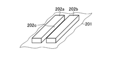
- FIG. 2A is a perspective view showing a state of an intermediate step for describing the method for manufacturing an optical device according to Embodiment 2 of the present invention.
- FIG. 2B is a perspective view showing a state of an intermediate step for describing the method for manufacturing an optical device according to Embodiment 2 of the present invention.
- FIG. 2C is a perspective view showing a state of an intermediate step for describing the method for manufacturing an optical device according to Embodiment 2 of the present invention.
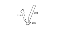
- FIG. 2D is a perspective view illustrating a state of an intermediate step for describing the method for manufacturing an optical device in the second embodiment of the present invention.
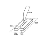
- FIG. 2E is a perspective view showing a state of an intermediate step for describing the method for manufacturing an optical device according to Embodiment 2 of the present invention.
- Embodiment 1 First, a method for manufacturing an optical device according to Embodiment 1 of the present invention will be described with reference to FIGS. 1A to 1F.
- a photonic crystal 101 is manufactured.
- the photonic crystal 101 includes a base 102 and a plurality of columnar lattice elements 103 formed on the base 102.
- the grating elements 103 are periodically provided on the base 102 at intervals equal to or less than the wavelength of the target light.
- the grating element 103 has a different refractive index from the base 102.
- the plurality of lattice elements 103 are arranged, for example, in a triangular lattice shape in plan view.
- the lattice element 103 is, for example, a cylindrical through hole that penetrates the base 102 from the front side to the back side, and is made of air.
- the photonic crystal 101 includes a nanoslot 104 at the center (resonator center) of a region to be a resonator.
- the photonic crystal 101 has the basic structure of an optical device that is a photonic crystal resonator.
- the nanoslot 104 is a rectangular parallelepiped hole.
- the base 102 is made of silicon, and the thickness of the base 102 is about 210 nm.
- the height of the lattice element 103 penetrating the base 102 is about 210 nm.
- the lattice constant a is about 460 nm, and the diameter of the lattice element 103 is about a / 4.
- the lattice element 103b also shifts in a direction away from the nanoslot 104, and the amount of this shift is about 0.50 times the amount of shift of the lattice element 103a.
- the length of the nanoslot 104 in the left-right direction of FIG. 1A may be about 400 nm, and the width of the nanoslot 104 may be about 30 to 70 nm.
- an electric field is concentrated on a single antinode in the nanoslot 104, and a nanoresonator mode in which the Q value is tens of thousands or more and the mode volume is significantly lower than 1 ( ⁇ / 2n) 3 can be realized.
- tens of thousands or more theoretical Q values are obtained.
- the width of the nanoslot 104 is set to about 40 nm, the highest Q value can be obtained.
- the refractive index is modulated not only in the nanoslot 104 but also in all the low refractive index portions including the lattice element 103, the performance of the Q value and the mode volume is maintained, but only the nanoslot 104 is filled with the active medium.
- the other grating elements 103 are left as air, the same high performance is maintained as when the low refractive index medium is all air.
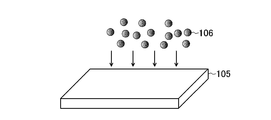
- particles 106 of an active medium are dispersed in a layer 105 serving as a base material, thereby forming a layer 107 of an active medium as shown in FIG. 1C (second step).
- the particles 106 are quantum dots, such as ZnS and ZnSe, which are smaller than the nanoslots 104 and are useful as a nanoluminescent material, and diamond nanoparticles containing a luminescent center such as a nitrogen impurity (NV center) or a Si impurity (SiV center).
- these fine particles are dispersed or doped as a guest medium in the layer 105 using a polymer such as PMMA (polymethylmethacrylate) as a host medium.
- a polymer such as PMMA (polymethylmethacrylate)
- the layer 107 the layer can be used as an active medium.
- the number and density of quantum dots and emission centers can be controlled by adjusting dispersion or doping.
- the layer 105 serving as the host medium a layer which can be easily formed into a film and does not impair the performance of the guest medium may be selected.
- a fluorescent dye such as DCM / AlQ 3 having a gain for realizing laser oscillation or a perovskite material having excellent light absorption characteristics can be formed as a thin film, and this thin film is used as the layer 107. It is possible. In any case, the thickness of the layer 107 is desirably the same as or less than the height of the nanoslots 104 to facilitate placement in the nanoslots 104.
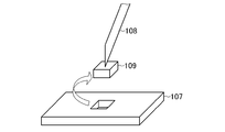
- a part of the layer 107 is taken out (cut out) by the nanoprobe 108 to form the active medium piece 109 (third step).
- an active medium in an amount necessary and operable by the nanoprobe 108 is extracted from the layer 107 to form an active medium piece 109.
- the layer 107 may be formed in advance to roughly required dimensions by a well-known lithography technique or an ion beam patterning technique. Just fine.
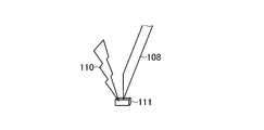
- the active medium piece 109 taken out by the nanoprobe 108 is processed in accordance with the shape of the nanoslot 104 to form a smaller processed active medium piece 111 as shown in FIG. 1E (fourth step).
- the active medium small piece 111 is formed (processed) into a three-dimensional shape suitable for being arranged inside the nanoslot 104 by irradiation with the ion beam 110.
- the processing into the active medium piece 111 is performed while being held by the nanoprobe 108.
- the processing using the ion beam 110 may be, for example, the use of a focused ion beam (FIB) method in a vacuum, which is currently widely used. Since the portion irradiated with the ion beam 110 is removed by etching, processing damage due to the ion beam on the shaped active medium piece 111 is minimized.
- FIB focused ion beam
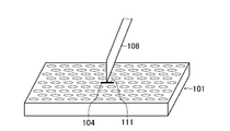
- the active medium small piece 111 taken out and processed by the nanoprobe 108 is arranged inside the nanoslot 104 (fifth step).
- the shape of the tip of the nanoprobe 108 cannot be said to be sufficiently large and narrow compared to the nanoslot 104 having a width of 100 nm or less.
- the shape of the active medium small piece 111 is adjusted to the nanoslot 104 in advance. Since the three-dimensional processing is performed, the arrangement in the nanoslot 104 becomes easy.
- Embodiment 2 Next, a method for manufacturing an optical device according to Embodiment 2 of the present invention will be described with reference to FIGS. 2A to 2E.
- a plasmon waveguide (optical device basic structure) composed of two metal patterns 202a and 202b is formed on a substrate 201 (first step).
- first step By setting the gap 202c between the metal pattern 202a and the metal pattern 202b to about 20 nm to 100 nm, the surface plasmon polariton due to the interaction between the surface plasmon and the light of the metal patterns 202a and 202b in the gap 202c is excited, and the plasmon mode is changed.
- Non-Patent Document 2 See Non-Patent Document 2.
- the confinement of the plasmon mode and the electric field strength are maximized by setting the thickness of the metal patterns 202a and 202b to about 20 nm (see Non-Patent Document 2).
- the thickness of the metal patterns 202a and 202b can be set to about 200 nm depending on the application.
- the nanoslot is arranged in the gap 202c between the metal pattern 202a and the metal pattern 202b in which the plasmon mode is realized.
- the nanoslot is the gap 202c.
- the cross-sectional shape of the assumed nanoslot (gap 202c) is rectangular, and the size is from 20 ⁇ 20 (nm) to 200 ⁇ 200 (nm).
- an active medium layer 203 is formed (second step).
- the active medium is formed of a layered material in which one or more two-dimensional unit layers are stacked.
- the layered material is, for example, a transition metal dichalcogenide such as graphene, hexagonal boron nitride (h-BN), boron phosphide (BP), WS 2 , and MoS 2 . These layered materials have recently been shown to exhibit very useful optical properties.
- the thickness of the layer 203 made of such a layered material is 10 nm or less.
- a heterostructure including a plurality of layered substances may be used. In this case, the thickness of the layer 203 is about several tens nm.
- a part of the layer 203 is taken out (cut out) by the nanoprobe 204 to produce an active medium piece 205 (third step).
- an active medium in an amount necessary and operable by the nanoprobe 204 is extracted from the layer 203 to form an active medium piece 205.
- the layer 203 may be formed in advance to roughly required dimensions by a well-known lithography technique or ion beam patterning technique. Just fine.
- the active medium piece 205 taken out by the nanoprobe 204 is processed according to the shape of the gap 202c, and as shown in FIG. 2D, a smaller processed active medium piece 206 is formed (fourth step).
- the active medium small piece 206 is formed (processed) into a three-dimensional shape suitable for being arranged inside the gap 202c by irradiation with the ion beam 210.
- the processing into the active medium small piece 206 is performed while being held by the nanoprobe 204.
- the processing by the ion beam 210 may be, for example, the use of the FIB method in a vacuum. Since the portion irradiated with the ion beam 210 is removed by etching, processing damage due to the ion beam on the shaped active medium piece 206 is minimized.
- the active medium small pieces 206 taken out and processed by the nanoprobe 204 are arranged inside the gap 202c (fifth step).
- the shape of the tip of the nanoprobe 204 cannot be said to be sufficiently large and narrow with respect to the gap 202c having a width of 100 nm or less.
- the shape of the active medium small piece 206 is three-dimensionally adjusted in advance to the gap 202c. Since it is processed, it is easy to perform the arrangement in the gap 202c.
- a part of the layer made of the active medium is taken out by the nanoprobe to form an active medium piece, and the active medium piece is processed into the shape of the nanoslot to be smaller. Since the active medium pieces are used, the desired active medium can be selectively arranged in the nanoslot by the nanoprobe.
- the nanoslot has a width of less than 200 nm, it has conventionally been difficult to selectively arrange an active medium only in the nanoslot.
- the active medium small pieces arranged in the slot do not necessarily fill the entire slot, and may have a gap.
- the embedding of the active medium small piece is not completed by one nanoprobe operation, but the embedding is realized by a plurality of operation repetitions, and small pieces of different active medium are put into the slot by multiple embedding operations. It may be accumulated.
- Reference Signs List 101 photonic crystal, 102 base, 103 lattice element, 104 nanoslot, 105 layer, 106 particle, 107 layer, 108 nanoprobe, 109 active material piece, 110 ion beam, 111 Active medium pieces.
Landscapes
- Physics & Mathematics (AREA)
- Engineering & Computer Science (AREA)
- General Physics & Mathematics (AREA)
- Optics & Photonics (AREA)
- Chemical & Material Sciences (AREA)
- Nanotechnology (AREA)
- Microelectronics & Electronic Packaging (AREA)
- Electromagnetism (AREA)
- Manufacturing & Machinery (AREA)
- Crystallography & Structural Chemistry (AREA)
- Condensed Matter Physics & Semiconductors (AREA)
- Plasma & Fusion (AREA)
- Health & Medical Sciences (AREA)
- General Health & Medical Sciences (AREA)
- Nuclear Medicine, Radiotherapy & Molecular Imaging (AREA)
- Radiology & Medical Imaging (AREA)
- Optical Integrated Circuits (AREA)
- Lasers (AREA)
Abstract
ナノプローブ(108)が取り出した活性媒質片(109)を、ナノスロット(104)の形状に合わせて加工し、より小さく加工した活性媒質小片(111)とする(第4工程)。例えば、イオンビーム(110)の照射により、ナノスロット(104)の内部に配置するために適した3次元形状に形成(加工)した活性媒質小片(111)とする。活性媒質小片(111)への加工は、ナノプローブ(108)で保持した状態で実施する。
Description
本発明は、幅が200nm以下のナノスロットを備える光デバイスの製造方法に関する。
フォトニック結晶は、屈折率の異なる2種類以上の媒体からなる周期結晶構造を有する人工素材であり、光の伝播・屈折・反射の制御や光の捕獲等の機能を有する。フォトニック結晶中には、結晶周期の数倍程度の寸法の小さな体積に光を閉じ込めるナノ共振器を配置することが可能である。近年は更に、幅が200nm以下の真空・空気ないし低屈折率媒体からなるスロット構造を、ナノ共振器中心に配置したフォトニック結晶共振器が提案されている(非特許文献1参照)。このスロット構造を用いたナノ共振器(スロットナノ共振器)では、適切な設計を与えることで、スロット内の電界を、スロットのない通常のナノ共振器に比べ大幅に増強できる。
スロットの幅は、フォトニック結晶周期よりも大幅に小さいため、スロットのない通常のナノ共振器に比べ、光閉じ込め体積は更に小さくなる。共振器モード体積(V)として、1(λ/2n)3(λ:波長、n:共振器中心の屈折率)を大きく下回る設計が、スロット配置により可能になる。この設計は、スロットのないナノ共振器では実現不可能とされている。
スロットナノ共振器においては、スロット内に光利得や光非線形効果を有する活性媒体、あるいは量子ドットやダイヤモンドNVセンターなどの発光中心を配置することで、これらと共振器モードとの光物質相互作用を著しく増強させ、高性能の光デバイスとして利用することが可能となる。また、スロットナノ共振器は、レーザー媒質や光吸収媒体として優れた特性を有し、最近研究開発が盛んにされているペロブスカイト系光学物質もスロットとの組み合わせで活性媒体として利用可能な有力候補である。
ところで、2つの金属パターンの間に、幅200nm以下の平行なナノギャップを設けたMIM(metal-insulator-metal)導波路の研究開発が進められている(非特許文献2参照)。MIM導波路では、プラズモンモードの電界をナノギャップ部分に強く閉じ込め、かつ電界強度を増強できることが示されている。この、MIMによるプラズモン導波路におけるナノギャップおよびナノギャップ内の電界は、寸法的にも物理的・物性的にも、前述したナノスロットと同等と考えることができる。スロット内に配置される活性媒質および作製に必要な技術および課題に関しては、スロットナノ共振器もナノギャッププラズモン導波路も共通であると考えてよい。
上述したナノスロット内への選択的な活性ナノ構造あるいは活性媒質を選択的に配置するためには、ナノファブリケーションが必要になる。しかしながら、現在、ナノスロット内への選択的な配置が可能な産業的に確立されたナノファブリケーション技術は存在しない。有力な技術として、ナノプローブを用いたポストプロセスがあげられる。ナノスケールの3次元表面観察が可能なAFM(Atomic Force Microscope)の技術を基本に、AFMプローブにより、ナノ物質を直接ピックアップし、ピックアップしたなの物質を移動して配置するAFMリソグラフィが研究されている(非特許文献3参照)。例えば、AFMプローブにより、流体の塗布を可能としたディップペンリソグラフィ装置が市販開始されている。
また、AFMプローブ機能を有しないナノプローブによるナノマニピュレーション技術も研究されている(非特許文献4参照)。
倉持 栄一 他、「H1スロットナノ共振器による高Q/V値の達成」、第64回応用物理学会春季学術講演会 講演予稿集、16a-F202-8、2017年。
M. ONO et al., "Deep-subwavelength plasmonic mode converter with large size reduction for Si-wire waveguide", Optical Society of America, vol. 3, no. 9, pp. 900-1005, 2016.
A. Yokoo et al., "Subwavelength Nanowire Lasers on a Silicon Photonic Crystal Operating at Telecom Wavelengths", American Chemical Society, vol. 4, pp. 355-362, 2017.
M. Ono et al., "Nanowire-nanoantenna coupled system fabricated by nanomanipulation", Optics Express, vol. 24, no. 8, pp. 8647-8659, 2016.
倉持 栄 他、「高 Q/V値 H1 スロットナノ共振器におけるスロット効果」、第78回応用物理学会秋季学術講演会 講演予稿集、6a-A405-1、2017年。
前述したナノスロットデバイスのスロット幅は、ナノスロットによる光強い閉じ込め効果および電界増強効果を得るために、通常100nmよりも大幅に狭い設計が用いられる。かつ、ナノスロットデバイスの性能を最大化するために、活性ナノ構造ないしナノ媒質は、スロット内のみに選択的に配置することが求められる。AFMリソグラフィなどの従来の製造技術では、ナノメートル単位の位置分解能および位置選択性は有している。
しかしながら、AFMをはじめとする従来のナノプローブでは、プローブ先端の曲率半径が100nmかそれ以上であり、ナノスロット内に活性媒質を選択的に充填配置するためにナノプローブの先端形状が十分鋭いとは言えない。現状のナノプローブにおいてスロット内に活性媒質を配置するためには、非特許文献3のナノワイヤのように、活性媒質がスロットに合わせた形状に自己形成されている必要がある。このため、活性媒質の形状がスロットに合わせた形状になっていない場合、あるいは量子ドットや発光中心を含むナノ粒子のようなスロットより小さいナノ活性媒体の場合、現在の技術では、ナノプローブによりスロット内に配置することができないという問題があった。
本発明は、以上のような問題点を解消するためになされたものであり、ナノプローブにより、所望とする活性媒質をナノスロットに選択的に配置できるようにすることを目的とする。
本発明に係る光デバイスの製造方法は、ナノスロットを備える光デバイス基本構造を作製する第1工程と、活性媒質による層を作製する第2工程と、ナノプローブにより層の一部を取り出して活性媒質片を形成する第3工程と、ナノプローブが取り出した活性媒質片をナノスロットの形状に合わせて加工してより小さい活性媒質小片とする第4工程と、ナノプローブにより取り出して加工した活性媒質小片をナノスロットに配置する第5工程とを備える。
上記光デバイスの製造方法において、活性媒質による層は、スロットより小さい活性媒質の粒子が分散されている。
上記光デバイスの製造方法において、第4工程では、イオンビームの照射により活性媒質片をナノスロットの形状に合わせて加工して活性媒質小片とする。
上記光デバイスの製造方法において、光デバイス基本構造は、フォトニック結晶共振器であり、ナノスロットは、共振器中心に配置されている。
上記光デバイスの製造方法において、光デバイス基本構造は、2つの金属パターンから構成されたプラズモン導波路であり、ナノスロットは、2つの金属パターンの間に配置されている。
以上説明したように、本発明によれば、ナノプローブにより活性媒質による層の一部を取り出して活性媒質片を形成し、この活性媒質片をナノスロットの形状に合わせて加工してより小さい活性媒質小片とするので、ナノプローブにより、所望とする活性媒質をナノスロットに選択的に配置できるという優れた効果が得られる。
以下、本発明の実施の形態おける光デバイスの製造方法について説明する。
[実施の形態1]
はじめに、本発明の実施の形態1における光デバイスの製造方法について、図1A~図1Fを参照して説明する。
はじめに、本発明の実施の形態1における光デバイスの製造方法について、図1A~図1Fを参照して説明する。
まず、図1Aに示すように、フォトニック結晶101を作製する。フォトニック結晶101は、基部102および基部102に形成された柱状の複数の格子要素103を備える。格子要素103は、対象とする光の波長以下の間隔で周期的に基部102に設けられている。また、格子要素103は、屈折率が基部102とは異なる。複数の格子要素103は、例えば平面視で三角格子状に配列している。格子要素103は、例えば、基部102を表面側から裏面側に貫通する円筒形状の貫通孔であり、空気から構成されている。
また、フォトニック結晶101は、共振器とする領域の中心部(共振器中心)に、ナノスロット104を備える。実施の形態1において、フォトニック結晶101は、フォトニック結晶共振器とする光デバイス基本構造である。また、ナノスロット104は、直方体状の孔部である。
フォトニック結晶101は、例えば、基部102がシリコンから構成され、基部102の板厚は、210nm程度である。基部102を貫通している格子要素103の高さは、210nm程度となる。また、例えば、格子定数aが460nm程度、格子要素103の直径は、a/4程度である。また、ナノスロット104の図1Aの紙面左右方向に配置されている格子要素103aは、ナノスロット104より離れる方向に、0.12a程度シフトしている。また、格子要素103bも、ナノスロット104より離れる方向にシフトし、このシフト量は、格子要素103aのシフト量の0.50倍程度とされている。
また、ナノスロット104の図1Aの紙面左右方向の長さは、400nm程度とし、ナノスロット104の幅は、30~70nm程度とすればよい。
上述した設定により、ナノスロット104内の単一アンチノードに電界が集中し、Q値が数万以上でモード体積が1(λ/2n)3を大きく下回るナノ共振器モードが実現できる。例えば、数万以上の理論Q値が得られる。特に、ナノスロット104の幅を40nm程度とすることで、最も高いQ値が得られる。
なお、非特許文献5に説明されているように、基部102をSiとしたまま、格子要素103の屈折率をn=1.5程度まで高めても共振器の基本性能は維持される。ナノスロット104のみではなく、格子要素103を含む全ての低屈折率部分の屈折率を変調した場合には、Q値やモード体積の性能が維持されるが、ナノスロット104のみに活性媒質を充填し、他の格子要素103は空気のままとした場合、低屈折率媒質が全て空気である場合とほぼ同等の高性能が維持される。
次に、図1Bに示すように、母材となる層105に活性媒質の粒子106を分散させることで、図1Cに示すように、活性媒質の層107を作製する(第2工程)。粒子106は、ナノスロット104より小さい、ナノ発光材料として有用なZnS,ZnSeなどの量子ドット、また窒素不純物(NVセンター)やSi不純物(SiVセンター)などの発光中心を含むダイヤモンドナノ粒子である。これらの微粒子は、ナノプローブによる直接操作や単体でのナノスロット104内への配置が困難であるが、PMMA(polymethyl methacrylate)などのポリマーをホスト媒体とした層105に、ゲスト媒体として分散ないしドーピングして層107とすることで、活性媒体として利用可能になる。量子ドットや発光中心の数や密度は、分散ないしドーピングの調整により制御できる。ホスト媒体となる層105は、フィルム化が容易で、かつゲスト媒体の性能を損なわないものを選択すればよい。
なお、レーザー発振を実現する利得を有するDCM/AlQ3のような蛍光色素や、優れた光吸収特性を有するペロブスカイト材料などは、薄膜として形成することが可能であり、この薄膜を層107として用いることが可能である。いずれにおいても、層107の厚さは、ナノスロット104内への配置が容易になるよう、ナノスロット104の高さと同じかより薄いことが望ましい。
次に、図1Dに示すように、ナノプローブ108により層107の一部を取り出し(切り出し)て、活性媒質片109を作製する(第3工程)。ナノプローブ108による取り出しにおいては、必要かつナノプローブ108で操作可能な量の活性媒質を層107より取り出し、活性媒質片109とする。後で整形するため、この時点で、活性媒質片109の形状を細かく制御する必要は無く、活性媒質片109の寸法が、要求よりも下回らなければ良い。なお、ナノプローブ108のみで必要な形状や量の活性媒質片109が取り出せない場合、よくしられたリソグラフィ技術やイオンビームによるパターニング技術により、予め大まかな必要な寸法に層107を成形しておけばよい。
次に、ナノプローブ108が取り出した活性媒質片109を、ナノスロット104の形状に合わせて加工し、図1Eに示すように、より小さく加工した活性媒質小片111とする(第4工程)。例えば、イオンビーム110の照射により、ナノスロット104の内部に配置するために適した3次元形状に形成(加工)した活性媒質小片111とする。ここで、活性媒質小片111への加工は、ナノプローブ108で保持した状態で実施する。
イオンビーム110による加工は、例えば、現在普及している真空中での集束イオンビーム(FIB)法の利用が考えられる。イオンビーム110が当たる部分は、エッチング除去されるため、整形後の活性媒質小片111におけるイオンビームによる加工損傷は最小限となる。非特許文献4に報告されているように、イオンビーム加工とナノプローブによる加工やマニピュレーションは、同一装置内に機能集積し連続的に実行可能である。
次に、図1Fに示すように、ナノプローブ108により取り出されて加工された活性媒質小片111をナノスロット104の内部に配置する(第5工程)。一般に、ナノプローブ108の先端の形状は、幅100nm以下のナノスロット104に対し大きく十分細いと言えないが、実施の形態1によれば、活性媒質小片111の形状が予めナノスロット104に合わせて3次元加工されているため、ナノスロット104内への配置が実施しやすくなる。
[実施の形態2]
次に、本発明の実施の形態2における光デバイスの製造方法について、図2A~図2Eを参照して説明する。
次に、本発明の実施の形態2における光デバイスの製造方法について、図2A~図2Eを参照して説明する。
まず、図2Aに示すように、基板201の上に、2つの金属パターン202a,202bから構成されたプラズモン導波路(光デバイス基本構造)を形成する(第1工程)。金属パターン202aと金属パターン202bとの隙間202cを、20nmから100nm程度とすることで、隙間202cにおける金属パターン202a,202bの表面プラズモンと光との相互作用による表面プラズモンポラリトンが励起し、プラズモンモードが実現される(非特許文献2参照)。
プラズモンモードの閉じ込めおよび電界強度は 金属パターン202a,202bの厚さを20nm程度にすることで最大化される(非特許文献2参照)。なお、金属パターン202a,202bの厚さは、用途に応じて200nm程度とすることが可能である。このように、プラズモンモードが実現される金属パターン202aと金属パターン202bとの間の隙間202cに、ナノスロットが配置される。言い換えると、実施の形態2におけるプラズモン導波路では、ナノスロットは、隙間202cである。想定されるナノスロット(隙間202c)の断面視の形状は矩形であり、寸法は、20×20(nm)から200×200(nm)である。
次に、図2Bに示すように、活性媒質の層203を形成する(第2工程)。実施の形態2において、活性媒質は、例えば、2次元的な単位層が、1層または複数層積層した層状物質から構成する。層状物質は、例えば、グラフェン、六方晶窒化ホウ素(h-BN)、リン化ホウ素(BP)、WS2,MoS2などの遷移金属ダイカルコゲナイドである。これらの層状物質は、非常に有用な光学物性を示すことが近年示されている。このような層状物質から構成される層203の厚さは10nm以下である。また、複数の層状物質によるヘテロ構造としてもよく、この場合、層203の厚さは数十nm程度となる。
次に、図2Cに示すように、ナノプローブ204により層203の一部を取り出し(切り出し)て、活性媒質片205を作製する(第3工程)。ナノプローブ204による取り出しにおいては、必要かつナノプローブ204で操作可能な量の活性媒質を層203より取り出し、活性媒質片205とする。後で整形するため、この時点で、活性媒質片205の形状を細かく制御する必要は無く、活性媒質片205の寸法が、要求よりも下回らなければ良い。なお、ナノプローブ204のみで必要な形状や量の活性媒質片205が取り出せない場合、よくしられたリソグラフィ技術やイオンビームによるパターニング技術により、予め大まかな必要な寸法に層203を成形しておけばよい。
次に、ナノプローブ204が取り出した活性媒質片205を、隙間202cの形状に合わせて加工し、図2Dに示すように、より小さく加工した活性媒質小片206とする(第4工程)。例えば、イオンビーム210の照射により、隙間202cの内部に配置するために適した3次元形状に形成(加工)した活性媒質小片206とする。ここで、活性媒質小片206への加工は、ナノプローブ204で保持した状態で実施する。
イオンビーム210による加工は、例えば、真空中でのFIB法の利用が考えられる。イオンビーム210が当たる部分は、エッチング除去されるため、整形後の活性媒質小片206におけるイオンビームによる加工損傷は最小限となる。
次に、図2Eに示すように、ナノプローブ204により取り出されて加工された活性媒質小片206を、隙間202cの内部に配置する(第5工程)。一般に、ナノプローブ204の先端の形状は、幅100nm以下の隙間202cに対し大きく十分細いと言えないが、実施の形態2によれば、活性媒質小片206の形状が予め隙間202cに合わせて3次元加工されているため、隙間202c内への配置が実施しやすくなる。
以上に説明したように、本発明によれば、ナノプローブにより活性媒質による層の一部を取り出して活性媒質片を形成し、この活性媒質片をナノスロットの形状に合わせて加工してより小さい活性媒質小片とするので、ナノプローブにより、所望とする活性媒質をナノスロットに選択的に配置できるようになる。
ナノスロットは、幅が200nmを下回るため、ナノスロット内のみに選択的に活性媒質を配置することは従来容易でなかった。特に、ナノプローブを用いてナノスロット内に活性媒質を確実に配置できる具体的技術の提示は従来無かった。従来は、スロットサイズに合わせた形状を有するナノワイヤなどを自己形成する必要があった。本発明により、ナノワイヤに限らず、ナノスロットの光物質相互作用増強効果を活用した様々な活性材料を利用したスロットデバイスの実現が容易にかつ現実的になる。
本発明において、スロット内に配置される活性媒質小片は、必ずしもスロット全体を充填せず、すき間が生じていても構わない。また、1回のナノプローブ操作で、活性媒質小片の埋め込み完了するのではなく、埋め込みが複数回の操作反復により実現され、また、異なる活性媒質の小片が、複数回の埋め込み操作でスロット内に集積されても構わない。
なお、本発明は以上に説明した実施の形態に限定されるものではなく、本発明の技術的思想内で、当分野において通常の知識を有する者により、多くの変形および組み合わせが実施可能であることは明白である。
101…フォトニック結晶、102…基部、103…格子要素、104…ナノスロット、105…層、106…粒子、107…層、108…ナノプローブ、109…活性媒質片、110…イオンビーム、111…活性媒質小片。
Claims (5)
- ナノスロットを備える光デバイス基本構造を作製する第1工程と、
活性媒質による層を作製する第2工程と、
ナノプローブにより前記層の一部を取り出して活性媒質片を形成する第3工程と、
前記ナノプローブが取り出した前記活性媒質片を前記ナノスロットの形状に合わせて加工してより小さい活性媒質小片とする第4工程と、
前記ナノプローブにより取り出して加工した前記活性媒質小片を前記ナノスロットに配置する第5工程と
を備えることを特徴とする光デバイスの製造方法。 - 請求項1記載の光デバイスの製造方法において、
前記層は、前記ナノスロットより小さい前記活性媒質の粒子が分散されていることを特徴とする光デバイスの製造方法。 - 請求項1または2記載の光デバイスの製造方法において、
前記第4工程では、イオンビームの照射により前記活性媒質片を前記ナノスロットの形状に合わせて加工して前記活性媒質小片とすることを特徴とする光デバイスの製造方法。 - 請求項1~3のいずれか1項に記載の光デバイスの製造方法において、
前記光デバイス基本構造は、フォトニック結晶共振器であり、
前記ナノスロットは、共振器中心に配置されている
ことを特徴とする光デバイスの製造方法。 - 請求項1~3のいずれか1項に記載の光デバイスの製造方法において、
前記光デバイス基本構造は、2つの金属パターンから構成されたプラズモン導波路であり、
前記ナノスロットは、前記2つの金属パターンの間に配置されている
ことを特徴とする光デバイスの製造方法。
Priority Applications (1)
| Application Number | Priority Date | Filing Date | Title |
|---|---|---|---|
| US17/252,788 US11300729B2 (en) | 2018-06-25 | 2019-06-04 | Method for manufacturing optical device |
Applications Claiming Priority (2)
| Application Number | Priority Date | Filing Date | Title |
|---|---|---|---|
| JP2018119531A JP6973305B2 (ja) | 2018-06-25 | 2018-06-25 | 光デバイスの製造方法 |
| JP2018-119531 | 2018-06-25 |
Publications (1)
| Publication Number | Publication Date |
|---|---|
| WO2020003918A1 true WO2020003918A1 (ja) | 2020-01-02 |
Family
ID=68984856
Family Applications (1)
| Application Number | Title | Priority Date | Filing Date |
|---|---|---|---|
| PCT/JP2019/022150 Ceased WO2020003918A1 (ja) | 2018-06-25 | 2019-06-04 | 光デバイスの製造方法 |
Country Status (3)
| Country | Link |
|---|---|
| US (1) | US11300729B2 (ja) |
| JP (1) | JP6973305B2 (ja) |
| WO (1) | WO2020003918A1 (ja) |
Families Citing this family (2)
| Publication number | Priority date | Publication date | Assignee | Title |
|---|---|---|---|---|
| EP3770652A1 (en) * | 2019-07-23 | 2021-01-27 | ETH Zurich | Diffractive optical element |
| CN114879288B (zh) * | 2022-04-27 | 2023-03-24 | 北京大学 | 同时发射多个单光子圆偏振光的准直发射器及其发射方法 |
Citations (3)
| Publication number | Priority date | Publication date | Assignee | Title |
|---|---|---|---|---|
| JP2014027168A (ja) * | 2012-07-27 | 2014-02-06 | Nippon Telegr & Teleph Corp <Ntt> | フォトニック結晶共振器の作製方法およびフォトニック結晶共振器 |
| JP2014204025A (ja) * | 2013-04-08 | 2014-10-27 | 日本電信電話株式会社 | カーボンナノチューブラマン光源およびこれに用いるシリコンフォトニック結晶共振器 |
| JP2015014653A (ja) * | 2013-07-03 | 2015-01-22 | 日本電信電話株式会社 | フォトニック結晶共振器 |
-
2018
- 2018-06-25 JP JP2018119531A patent/JP6973305B2/ja active Active
-
2019
- 2019-06-04 WO PCT/JP2019/022150 patent/WO2020003918A1/ja not_active Ceased
- 2019-06-04 US US17/252,788 patent/US11300729B2/en active Active
Patent Citations (3)
| Publication number | Priority date | Publication date | Assignee | Title |
|---|---|---|---|---|
| JP2014027168A (ja) * | 2012-07-27 | 2014-02-06 | Nippon Telegr & Teleph Corp <Ntt> | フォトニック結晶共振器の作製方法およびフォトニック結晶共振器 |
| JP2014204025A (ja) * | 2013-04-08 | 2014-10-27 | 日本電信電話株式会社 | カーボンナノチューブラマン光源およびこれに用いるシリコンフォトニック結晶共振器 |
| JP2015014653A (ja) * | 2013-07-03 | 2015-01-22 | 日本電信電話株式会社 | フォトニック結晶共振器 |
Also Published As
| Publication number | Publication date |
|---|---|
| US20210215877A1 (en) | 2021-07-15 |
| JP6973305B2 (ja) | 2021-11-24 |
| JP2020004753A (ja) | 2020-01-09 |
| US11300729B2 (en) | 2022-04-12 |
Similar Documents
| Publication | Publication Date | Title |
|---|---|---|
| Hsieh et al. | Perovskite quantum dot lasing in a gap-plasmon nanocavity with ultralow threshold | |
| US8509276B2 (en) | Plasmon lasers at deep subwavelength scale | |
| Livneh et al. | Highly directional room-temperature single photon device | |
| Scherer et al. | Photonic crystals for confining, guiding, and emitting light | |
| Oulton | Surface plasmon lasers: sources of nanoscopic light | |
| De La Rue et al. | Photonic crystal devices: some basics and selected topics | |
| Nonahal et al. | Engineering quantum nanophotonic components from hexagonal boron nitride | |
| Sun et al. | Lead halide perovskite nanoribbon based uniform nanolaser array on plasmonic grating | |
| JP6973305B2 (ja) | 光デバイスの製造方法 | |
| Kuramochi | Manipulating and trapping light with photonic crystals from fundamental studies to practical applications | |
| Su et al. | Tuning photoluminescence of CsPbBr3 quantum dots through plasmonic nanofingers | |
| Yang et al. | Strain tunable quantum dot based non-classical photon sources | |
| Alekseev et al. | Engineering whispering gallery modes in MoSe2/WS2 double heterostructure nanocavities: Towards developing all-TMDC light sources | |
| CN114865450A (zh) | 一种基于耦合纳米线对的极强场约束激光器 | |
| Yokoo et al. | Ultrahigh-Q nanocavities written with a nanoprobe | |
| Oh et al. | Self-aligned active quantum nanostructures in photonic crystals via selective wet-chemical etching | |
| CN109782455B (zh) | 一种单层二维材料中能谷光子的分离方法及分离装置 | |
| Song et al. | Enhanced light–matter interaction in plasmonic nanocavities: principle, challenge, and perspective | |
| Alekseev et al. | Engineering whispering gallery modes in MoSe $ _2 $/WS $ _2 $ double heterostructure nanocavities: Towards developing all-TMDC light sources | |
| Wang et al. | Large-angle twisted photonic crystal semiconductor nanolasers with ultra-low thresholds operating in the C-band | |
| Staude et al. | All-dielectric resonant meta-optics goes active | |
| Nguyen et al. | Coupling of a single active nanoparticle to a polymer-based photonic structure | |
| KR102700571B1 (ko) | 고집적 광회로의 광원 및 이를 제조하는 방법 | |
| EP4077209A1 (en) | Single-photon optical device | |
| Sinclair et al. | An introduction to quantum dots: confinement, synthesis, artificial atoms and applications |
Legal Events
| Date | Code | Title | Description |
|---|---|---|---|
| 121 | Ep: the epo has been informed by wipo that ep was designated in this application |
Ref document number: 19825943 Country of ref document: EP Kind code of ref document: A1 |
|
| NENP | Non-entry into the national phase |
Ref country code: DE |
|
| 122 | Ep: pct application non-entry in european phase |
Ref document number: 19825943 Country of ref document: EP Kind code of ref document: A1 |