WO2019212043A1 - 光学活性増強基板 - Google Patents
光学活性増強基板 Download PDFInfo
- Publication number
- WO2019212043A1 WO2019212043A1 PCT/JP2019/017931 JP2019017931W WO2019212043A1 WO 2019212043 A1 WO2019212043 A1 WO 2019212043A1 JP 2019017931 W JP2019017931 W JP 2019017931W WO 2019212043 A1 WO2019212043 A1 WO 2019212043A1
- Authority
- WO
- WIPO (PCT)
- Prior art keywords
- optical activity
- spiral
- nanoflower
- substrate
- shape
- Prior art date
- Legal status (The legal status is an assumption and is not a legal conclusion. Google has not performed a legal analysis and makes no representation as to the accuracy of the status listed.)
- Ceased
Links
Images





Classifications
-
- G—PHYSICS
- G01—MEASURING; TESTING
- G01N—INVESTIGATING OR ANALYSING MATERIALS BY DETERMINING THEIR CHEMICAL OR PHYSICAL PROPERTIES
- G01N21/00—Investigating or analysing materials by the use of optical means, i.e. using sub-millimetre waves, infrared, visible or ultraviolet light
- G01N21/17—Systems in which incident light is modified in accordance with the properties of the material investigated
- G01N21/41—Refractivity; Phase-affecting properties, e.g. optical path length
-
- G—PHYSICS
- G01—MEASURING; TESTING
- G01N—INVESTIGATING OR ANALYSING MATERIALS BY DETERMINING THEIR CHEMICAL OR PHYSICAL PROPERTIES
- G01N21/00—Investigating or analysing materials by the use of optical means, i.e. using sub-millimetre waves, infrared, visible or ultraviolet light
- G01N21/62—Systems in which the material investigated is excited whereby it emits light or causes a change in wavelength of the incident light
- G01N21/63—Systems in which the material investigated is excited whereby it emits light or causes a change in wavelength of the incident light optically excited
- G01N21/65—Raman scattering
Definitions
- the present invention relates to an optical activity enhancement substrate.
- ⁇ Chirality is the symmetry of molecules and determines the physical, chemical and biological properties of substances on a wide range of scales ranging from bulk crystals to nanomaterials and even biomolecules.
- the chirality of a molecule is the ability of a chiral molecule to selectively interact with left-handed circularly polarized light (LCP) or right-handed circularly polarized light (RCP), which is expressed by optical activity. Is done.
- a metal nanostructure as a basic component.
- This metal nanostructure is artificially induced by inducing surface plasmon resonance (SPR) on the nanostructure. It has been demonstrated that large optical activity can be realized (see Non-Patent Documents 3 to 6 below).
- SPR is resonant vibration due to free electrons in a metal coupled to an incident electromagnetic field. Since the electric field is strongly focused in the near-field region of the metal nanostructure due to the induction of SPR, the interaction between the metal nanostructure and the incident circularly polarized light is enhanced, and a large optical activity can be realized.
- a helical propeller type, a helical type, a scaffold type, a supramolecular structure, a multilayer connection structure, a pseudochiral structure, and the like have been proposed.
- Patent Documents 1 and 2 listed below disclose surface-enhanced Raman spectroscopy (SERS) that enhances Raman scattered light using metal nanostructures.
- the metal materials that make up the metal nanostructures are low in energy efficiency and high heat generation due to their inherent high ohmic loss, so their performance and practicality, such as destruction of organic molecules to be observed and occurrence of alteration, etc. Was insufficient.
- An object of the present invention is to provide an optical activity enhancement substrate having a high optical activity enhancement effect and a low ohmic loss.
- the present invention includes the following embodiments:
- the spiral nanoflower has a plurality of elliptical cylinders arranged between 4 and 8 around the cylinder, and a straight line connecting the center of the circle which is the cross section of the cylinder and the center of the ellipse which is the cross section of the elliptic cylinder
- An optically active enhancement substrate having a pseudo-propeller shape in which the major axis of the ellipse is inclined 45 to 55 degrees clockwise with respect to the above.
- CID (I R ⁇ I L ) / (I R + I L ) (2)
- I R is the intensity of the scattered light RCP
- I L is scattered light intensity of the LCP.
- an optical activity enhancement substrate having a high optical activity enhancement effect and a low ohmic loss.
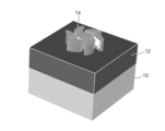
- FIG. 1 shows a configuration example of the optical activity enhancement substrate according to the embodiment.
- an optical activity enhancement substrate 100 includes a support substrate 10, an oxide layer 12 formed on one main surface of the support substrate 10, and a main surface on the opposite side of the oxide layer 12 from the support substrate 10. And the helical nanoflower 14 formed in the above.
- the support substrate 10 is formed of a material selected from silicon dioxide, titanium oxide, silicon, metallic glass, polymer, and metal, and can be appropriately determined depending on the application as long as it has a flat plate shape.
- the metal glass for example, Au 75 Si 25, alloys, such as chalcogenide glass can be used.
- the polymer for example, an aromatic heterocyclic polymer such as polythiophene, a conjugated polymer such as polyacetylene, or the like can be used.
- Au, Ag, Al etc. can be used, for example.
- the oxide layer 12 is formed of a material containing silica and aluminum oxide. Moreover, TiO 2 may be included. This oxide layer 12 can be formed by thermal oxidation.
- the spiral nanoflower 14 is made of a material (dielectric material) selected from silicon, germanium, titanium oxide, zinc telluride, and indium gallium arsenide, and is opposite to the support substrate 10 of the oxide layer 12. It is preferable to form a plurality on the main surface on the side. The shape and number of the spiral nanoflowers 14 will be described later.
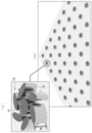
- FIGS. 2 (a) and 2 (b) show examples of the shape and arrangement of spiral nanoflowers.
- Fig.2 (a) shows the example of the shape of a spiral nanoflower
- FIG.2 (b) has shown the example of arrangement
- the spiral nanoflower 14 includes a cylinder 16 and an elliptic cylinder 18 arranged around the cylinder 16.
- a cylinder 16 and an elliptic cylinder 18 arranged around the cylinder 16.
- six elliptical cylinders 18 are arranged, but the present invention is not limited to this, and a plurality of elliptical cylinders 18 can be arranged between four and eight.
- the spiral nanoflower 14 has a major axis of the ellipse of 45 to 55 degrees clockwise with respect to a straight line connecting the center of the circle which is the cross section of the cylinder 16 and the center of the ellipse which is the cross section of the elliptic cylinder 18. More preferably, it has a pseudo propeller shape inclined by 50 degrees. As shown in FIG.
- geometric parameters defining the shape of the spiral nanoflower 14 in this case include a major axis length a, a minor axis length b of the ellipse, a radius r of the circle,
- the geometric parameter By making the geometric parameter the above numerical value, the contribution of the magnetic quadrupole of the spiral nanoflower 14 to the scattered light when the incident light is scattered by the spiral nanoflower 14 can be optimized, and the incident light Optical activity can be enhanced. That is, the spiral nanoflower 14 composed of the cylinder 16 and the elliptical column 18 has a shape in which electromagnetic resonance is excited, and can confine the electromagnetic field of light to vibrate and enhance it.
- optical activity C is represented by the following formula (1).
- E is an electric field
- B is a magnetic field
- ⁇ 0 is a dielectric constant
- ⁇ 0 is a magnetic permeability.
- Enhancing optical activity means increasing the value of optical activity represented by the above formula (1).
- the spiral nanoflower 14 according to the embodiment is formed of a dielectric material, and the dielectric material has a low ohmic loss. Therefore, by utilizing this property, the optical activity enhancement substrate having a low ohmic loss is used. Can be realized.
- spiral nanoflower 14 Other shapes include a spiral shape such as a spiral shape or a saddle shape formed of a spiral oligomer.
- the arrangement of the spiral nanoflowers 14 is arranged as a square lattice array arranged at a constant period on the main surface of the oxide layer 12, and the optical activity enhancement substrate according to the embodiment. Is configured.
- the period of the array is preferably 1 to 5 ⁇ m.
- the inclination of the elliptic cylinder 18 is changed (for example, the center of the circle that is the cross section of the cylinder 16 and the center of the ellipse that is the cross section of the elliptic cylinder 18).
- a scattered light with enhanced LCP can also be obtained.
- FIG. 3 shows a manufacturing process of the optical activity enhancement substrate according to the embodiment.
- a chip in which a support substrate 10, an oxide layer 12, and a dielectric material layer 20 are laminated in this order is prepared (I), and a negative resist film 22 is spin-coated on the dielectric material layer 20 (II). ).
- the array pattern of spiral nanoflowers is transferred to the dielectric material layer 20 by inductively coupled plasma using a mixed gas such as CHF 3 and SF 6 , and the remaining negative resist film 22 is diluted with dilute hydrofluoric acid. Remove (IV).
- the optical activity enhancement substrate according to the embodiment is manufactured.
- optical activity enhancement substrate according to the example was manufactured by the method shown in FIG. The specific procedure is as follows.
- a silicon-on-insulator (SOI) chip Soitec 8 inch (200 mm) wafer having a thickness of the upper silicon layer (dielectric material layer 20) of 340 nm was prepared, and a spin coater (SPS-Europe SPIN150i) was prepared. ) was applied by spin coating to a 300 nm thick HSQ negative resist film (manufactured by Tokyo Ohka Kogyo Co., Ltd.).
- SOI silicon-on-insulator
- an array pattern of spiral nanoflowers 40 ⁇ 40 square lattice array patterns were defined on an HSQ negative resist film by electron beam lithography using F7000S-VD02 manufactured by Advantest Corporation.
- the period of the square lattice array was 5 ⁇ m.
- the chip was developed with an NMD-3 solution (Tokyo Ohka Kogyo Co., Ltd., tetramethylammonium hydroxide solution) as a developer for 10 minutes and washed with pure water for 5 minutes.
- NMD-3 solution Tokyo Ohka Kogyo Co., Ltd., tetramethylammonium hydroxide solution
- etching is performed by inductively coupled plasma using a mixed gas of CHF 3 and SF 6 to form a square array pattern of spiral nanoflowers on the upper silicon. Transferred to the layer. Finally, the remaining HSQ negative resist was removed with dilute hydrofluoric acid (manufactured by Fuji Film Wako Pure Chemical Industries, Ltd.) to obtain an optical activity enhancing substrate.
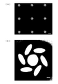
- FIGS. 4A and 4B Scanning electron microscope (SEM manufactured by Hitachi, Ltd.) images of the surface on which the spiral nanoflowers of the obtained optical activity enhancement substrate are formed are shown in FIGS.
- the scale bar displayed in FIG. 4A is 1 ⁇ m, and an array pattern of spiral nanoflowers is shown.
- the scale bar displayed in FIG. 4B is 100 nm, and a single spiral nanoflower is shown.
- FIGS. 4A and 4B it can be seen that a spiral nanoflower array is formed on the oxide layer of the optical activity enhancing substrate.
- a spiral nanoflower array without the column 16 was also manufactured as a comparative example.
- 5A and 5B show SEM images of the helical nanoflower array of the comparative example.
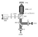
- FIG. 6 shows the configuration of the measurement apparatus (dark field microscope).
- a wide-area tungsten / halogen light source (SLS201L manufactured by Thorlabs) was used as a light source for incident light.
- the circular polarization state of the incident light was adjusted by the combined use of a linear polarizing plate LP (Thorlabs LPVIS050) and an achromatic quarter-wave plate QWP (Thorlabs AQWP05M-980). Incident light was incident in the direction of the spiral nanoflower array (Chip) via the beam splitter BS1.
- an objective lens with a low numerical aperture (Olympus UPLSAPO 10 ⁇ 0.40 NA) was used to focus the incident light on the spiral nanoflower array. .
- the reflected beam was blocked using a beam blocker to form a dark field.
- Scattered light from the helical nanoflower array was collected by an objective lens and then split into two beams by a beam splitter BS2.
- One beam was incident on the alignment CCD camera via the lens L1, and the nanoflower array was imaged and aligned.
- the other beam was sent to the spectrometer (CCS175, manufactured by Thorlabs) via the lens L2, and the scattering spectrum of the spiral nanoflower array was measured.
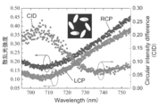
- FIGS. 7A and 7B show the measurement results of the scattering spectrum of the spiral nanoflower array when RCP and LCP are incident, measured as described above.
- FIG. 7A is a spectrum of scattered light intensity of the scattered spectrum
- FIG. 7B is a circular intensity difference (CID) obtained from the spectrum of scattered light intensity by the following equation (2). Distribution.
- CID (I R ⁇ I L ) / (I R + I L ) (2)
- I R is the intensity of the scattered light RCP
- the I L is scattered light intensity of the LCP.
- the scattered light intensity of RCP is higher than the scattered light intensity of LCP.
- the value of CID has a peak of 35% at a wavelength of 713 nm. This is an effect in which the geometric parameter of the spiral nanoflower is the above value.
- the optical activity-enhancing substrate provided with the spiral nanoflower array has realized a huge optical activity.
- FIG. 8 shows a measurement result of a scattering spectrum and a distribution of CID when RCP and LCP are incident on a substrate including a spiral nanoflower array according to a comparative example.
- the maximum CID value is about 25%, which is lower than the maximum CID in the case of the optical activity enhancement substrate of the embodiment shown in FIG. 7B. This indicates that the optical activity has decreased.
- the decrease in CID is due to the disappearance of interference between the central cylinder and the surrounding elliptic cylinder in the spiral nanoflower of the comparative example.
- a measurement sample ((+) ⁇ -pinene) having chirality is placed in a cuvette having an optical path length of 0.75 mm, and the optical activity enhancing substrate according to the example is disposed so that the support substrate 10 is in contact with the inner wall in the cuvette. And immersed in a measurement sample.
- the thickness of the measurement sample on the surface on which the spiral nanoflowers of the optical activity enhancing substrate are formed is 0.75 mm.
- the cuvette was irradiated with excitation light, and the Raman optical activity of the measurement sample was measured.
- a self-made measuring device was used for the measurement.
- the excitation light is laser light having a wavelength of 561 nm generated by a semiconductor laser generator manufactured by Coherent INC.
- FIG. 9 shows the configuration of the Raman optical activity measuring apparatus.
- the semiconductor laser generator is used as a light source for incident light.
- the circularly polarized state of incident light includes a linearly polarizing plate LP (Thorlabs LPVISC050), an achromatic quarter-wave plate QWP (Torlabs AQWP05M-561), a liquid crystal modulator LCM (Thorlabs LCC1411-A) and Techno. Adjustment was performed by using a half-wave plate with a rotary mount (WPQ05M-561, Thorlabs) R-HWP set in a hands motor, a hollow motor. Incident light was incident in the direction of the spiral nanoflower array (Chip) via the beam splitter BS.
- WPQ05M-561, Thorlabs rotary mount
- a measurement sample on the spiral nanoflower array is used to focus the incident light using a low numerical aperture objective lens (Olympus UPLSAPO 10 ⁇ 0.40 NA).
- a low numerical aperture objective lens Opalympus UPLSAPO 10 ⁇ 0.40 NA.
- Raman scattered light from the measurement sample enhanced by the helical nanoflower array is collected by the objective lens, then redirected by the beam splitter BS, through the notch filter, depolarizer, and through the lens L to the spectrometer (Oxford -It was sent to Kymera 193i Spectrograph & Andor Newton 920) manufactured by Instruments, and Raman scattered light was measured.
- the same measurement sample as the above measurement sample was placed on a slide glass, and Raman optical activity was measured using the same measurement apparatus.
- FIG. 10 shows the measurement results of the Raman optical activity of the optical activity enhancement substrate according to the example and the slide glass as a comparative example.
- the Raman scattered light intensity is shown together with the Raman optical activity.
- the Raman optical activity and the Raman scattered light intensity are enhanced about 10 times by the optical activity enhancing substrate according to the example as compared with the case of the slide glass.
Landscapes
- Health & Medical Sciences (AREA)
- Physics & Mathematics (AREA)
- Life Sciences & Earth Sciences (AREA)
- Chemical & Material Sciences (AREA)
- Analytical Chemistry (AREA)
- Biochemistry (AREA)
- General Health & Medical Sciences (AREA)
- General Physics & Mathematics (AREA)
- Immunology (AREA)
- Pathology (AREA)
- Nuclear Medicine, Radiotherapy & Molecular Imaging (AREA)
- Investigating, Analyzing Materials By Fluorescence Or Luminescence (AREA)
Abstract
【課題】光学活性の増強効果が高く、オーミック損失の低い光学活性増強基板を提供する。 【解決手段】光学活性増強基板は、支持基板10と、支持基板10の一方の主面上に形成された酸化層12と、酸化層12の支持基板10とは反対側の主面上に形成された螺旋状ナノフラワー14と、を備え、螺旋状ナノフラワー14は、円柱16の周囲に楕円柱18が複数配置され、円柱16の断面である円の中心と楕円柱18の断面である楕円の中心とを結ぶ直線に対して楕円の長軸が時計回りに45度傾いている擬似プロペラ形状である。
Description
本発明は、光学活性増強基板に関する。
キラリティーは分子の対称性であり、バルク結晶からナノ材料、さらには生体分子におよぶ広範な大きさのスケールで、物質の物理・化学・生物学的特性を決定付ける。分子のキラリティーは、一般に、キラル分子が持つ左回り円偏光(left circular polarized:LCP)または右回り円偏光(right circular polarized:RCP)と選択的に相互作用する能力であり、光学活性によって表される。
このような光学活性は、立体化学、分析化学、メタマテリアル、スピンフォトニクス、および宇宙生物学において極めて重要な効果であるが、天然分子等の光学活性は、本来非常に小さい効果であるので、これを増強する技術が検討されている(下記非特許文献1、2参照)。
特に、金属ナノ構造を基本的な構成要素として利用することが提唱されており、この金属ナノ構造は、ナノ構造上に表面プラズモン共鳴(surface plasmon resonance:SPR)を誘起することで、人工的に大きな光学活性が実現できることが実証されている(下記非特許文献3~6参照)。SPRは、入射電磁場と結合した、金属中の自由電子による共鳴振動である。SPRの誘起によって金属ナノ構造の近接場領域で電場が強く収束するので、金属ナノ構造と入射円偏光との相互作用が増強され、大きな光学活性を実現できる。このような金属ナノ構造としては、螺旋状プロペラ型、螺旋型、足場型、超分子構造、多層連結構造及び擬キラル構造等が提案されている。
また、下記特許文献1、特許文献2には、金属ナノ構造を使用したラマン散乱光を増強する表面増強ラマン分光(SERS)が開示されている。
しかし、金属ナノ構造を構成する金属材料は、固有の高いオーミック損失のためにエネルギー効率が低く、かつ高発熱であるため、観測対象の有機分子の破壊、変質の発生等、その性能と実用性は不十分であった。
Y. Cui, L. Kang, S. Lan, S. Rodrigues, W. Cai, Nano Lett. 2014, 14, 1021.
J. Lv, K. Hou, D. Ding, D. Wang, B. Han, X. Gao, M. Zhao, L. Shi, J. Guo, Y. Zheng, X. Zhang, C. Lu, L. Huang, W. Huang, Z. Tang, Angew. Chem. Int. Ed. 2017, 56, 5055.
M. Hentschel, M. Schaferling, X. Y. Duan, H. Giessen, N. Liu, Sci, Adv, 2017, 3, e1602735,
A. Kuzyk, R. Schreiber, Z. Y. Fan, G. Pardatscher, E. M. Roller, A. Hogele, F. C. Simmel, A. O. Govorov, T. Liedl, Nature 2012, 483, 311.
E. Hendry, R. V. Mikhaylovskiy, L. D. Barron, M. Kadodwala, T. J. Davis, Nano Lett, 2012, 12, 3640.
S. Zu, Y. Bao, Z. Fang, Nanoscale 2016, 8, 3900.
本発明は、光学活性の増強効果が高く、オーミック損失の低い光学活性増強基板を提供することを目的とする。
上記目的を達成するために、本発明は以下の実施態様を含む
[1]支持基板と、前記支持基板の一方の主面上に形成された酸化層と、前記酸化層の前記支持基板とは反対側の主面上に形成された螺旋状ナノフラワーと、を備え、前記螺旋状ナノフラワーは、円柱の周囲に楕円柱が4個から8個の間で複数配置され、円柱の断面である円の中心と楕円柱の断面である楕円の中心とを結ぶ直線に対して前記楕円の長軸が時計回りに45~55度傾いている擬似プロペラ形状である光学活性増強基板。
[2]前記支持基板は、二酸化ケイ素、酸化チタン、シリコン、金属ガラス、高分子、金属から選択された物質により形成される、[1]に記載の光学活性増強基板。
[3]前記酸化層は、シリカと酸化アルミニウムを含む材料により形成される、[1]または[2]に記載の光学活性増強基板。
[4]前記螺旋状ナノフラワーは、シリコン、ゲルマニウム、酸化チタン、テルル化亜鉛、リン化インジウムガリウムヒ素から選択された物質により形成される[1]から[3]のいずれか一項に記載の光学活性増強基板。
[5]前記螺旋状ナノフラワーの形状が、前記擬似プロペラ形状の代わりに、螺旋状オリゴマーで形成される螺旋形状または卍型形状のいずれかである、[1]から[4]のいずれか一項に記載の光学活性増強基板。
[6]前記螺旋状ナノフラワーは、電磁気共鳴が励起される形状である、[1]から[5]のいずれか一項に記載の光学活性増強基板。
[7]前記螺旋状ナノフラワーの形状は、以下の式(2)で得られる円偏光強度差(CID)の値を最大化するように決定される、[1]から[6]のいずれか一項に記載の光学活性増強基板。
CID=(IR-IL)/(IR+IL)・・・(2)
なお、IRはRCPの散乱光強度、ILはLCPの散乱光強度である。
CID=(IR-IL)/(IR+IL)・・・(2)
なお、IRはRCPの散乱光強度、ILはLCPの散乱光強度である。
本発明によれば、光学活性の増強効果が高く、オーミック損失の低い光学活性増強基板を提供できる。
図1には、実施形態にかかる光学活性増強基板の構成例が示される。図1において、光学活性増強基板100は、支持基板10と、支持基板10の一方の主面上に形成された酸化層12と、酸化層12の上記支持基板10とは反対側の主面上に形成された螺旋状ナノフラワー14とを含んで構成されている。
支持基板10は、二酸化ケイ素、酸化チタン、シリコン、金属ガラス、高分子、金属から選択された物質により形成され、平板状であれば用途に応じて適宜形状を決定できる。上記金属ガラスとしては、例えばAu75Si25、カルコゲナイドガラス等の合金が使用できる。また、上記高分子としては、例えばポリチオフェン等の芳香族複素環ポリマー、ポリアセチレン等の共役ポリマー等が使用できる。また、上記金属としては、例えばAu、Ag、Al等が使用できる。
酸化層12は、シリカと酸化アルミニウムを含む材料により形成される。また、TiO2が含まれていてもよい。この酸化層12は、熱酸化により形成することができる。
螺旋状ナノフラワー14は、シリコン、ゲルマニウム、酸化チタン、テルル化亜鉛、リン化インジウムガリウムヒ素から選択された物質(誘電物質)により形成されており、上記酸化層12の上記支持基板10とは反対側の主面上に複数形成されるのが好適である。螺旋状ナノフラワー14の形状及び数については後述する。
図2(a)、(b)には、螺旋状ナノフラワーの形状及び配置の例が示される。図2(a)が、螺旋状ナノフラワーの形状の例を示し、図2(b)が配置例を示している。
図2(a)において、螺旋状ナノフラワー14は、円柱16と、円柱16の周囲に配置され楕円柱18により構成されている。図2(a)の例では、楕円柱18が6個配置されているが、これには限定されず、4個から8個の間で複数配置することができる。
また、螺旋状ナノフラワー14は、円柱16の断面である円の中心と楕円柱18の断面である楕円の中心とを結ぶ直線に対して上記楕円の長軸が時計回りに45~55度、より好適には50度傾いている擬似プロペラ形状となっている。この場合の螺旋状ナノフラワー14の形状を規定する幾何学的パラメータは、図2(a)に示されるように、上記楕円の長軸長a、短軸長b、上記円の半径r、上記円の中心と上記楕円の頂点との距離の内短い方の距離d及び円柱16と楕円柱18の高さhであり、a=128~1280nm(好適には425nm)、b=38~380nm(好適には125nm)、r=56~560nm(好適には187nm)、d=75~750nm(好適には250nm)、h=102~1020nm(好適には340nm)が好適である。幾何学的パラメータを上記数値とすることにより、入射光が螺旋状ナノフラワー14で散乱される際の散乱光に対する螺旋状ナノフラワー14の磁気四重極の寄与度を最適化でき、入射光の光学活性を増強することができる。すなわち、円柱16及び楕円柱18で構成された螺旋状ナノフラワー14は、電磁気共鳴が励起される形状となっており、光の電磁場を閉じ込めてこれを振動させ、増強することができる。
ここで、光学活性Cは、以下の式(1)で示される。
 なお、Eは電場、Bは磁場、ε0は誘電率、μ0は透磁率である。
光学活性を増強するとは、上記式(1)で示される光学活性の値を大きくすることをいう。
光学活性を増強するとは、上記式(1)で示される光学活性の値を大きくすることをいう。
また、上述したように、実施形態にかかる螺旋状ナノフラワー14は、誘電物質により形成されており、誘電物質は、オーミック損失が低いので、この性質を利用してオーミック損失の低い光学活性増強基板を実現できる。
螺旋状ナノフラワー14の他の形状として、螺旋状オリゴマーで形成される螺旋形状または卍型形状等の螺旋状の形状が挙げられる。
螺旋状ナノフラワー14の配置は、図2(b)に示されるように、酸化層12の主面上に、一定周期で配置された正方格子アレイとして配列され、実施形態にかかる光学活性増強基板を構成している。この場合のアレイの周期(螺旋状ナノフラワー14の円柱16の中心線の間の距離)は1~5μmが好適である。
図2(b)に示された光学活性増強基板に、LCP(左回り円偏光)またはRCP(右回り円偏光)のビームを光学活性増強基板上の螺旋状ナノフラワーに直角に当てると、入射光と螺旋状ナノフラワーとの相互作用により、図2(a)に示される螺旋状ナノフラワー14の場合、RCPが強調された散乱光となる。この際に、光学活性増強基板上に右旋性のキラリティーを有する試料を載せてRCPのビームを照射すると、散乱光のRCPが増強され、これに比例して試料の光学活性も増強されるので、この散乱光を収集して試料の定性分析、定量分析を精度高く実施することができる。例えば、ラマン分光法において、ラマン光学活性を増強して測定精度の向上、測定時間の短縮等を図ることができる。
なお、図2(a)に示された螺旋状ナノフラワー14において、楕円柱18の傾きを変更する(例えば、円柱16の断面である円の中心と楕円柱18の断面である楕円の中心とを結ぶ直線に対して上記楕円の長軸を反時計回りに50度傾ける)ことにより、LCPが強調された散乱光を得ることもできる。
図3には、実施形態にかかる光学活性増強基板の製造工程が示される。図3において、支持基板10、酸化層12、誘電物質層20がこの順に積層されたチップを準備し(I)、上記誘電物質層20の上に、ネガ型レジストフィルム22をスピンコーティングする(II)。
次に、螺旋状ナノフラワーのアレイパターンを電子ビームリソグラフィーによってレジストフィルム上に画定し、現像液で現像した後に純水で洗浄する(III)。
次に、CHF3とSF6等の混合ガスを用いた誘導結合プラズマによって、螺旋状ナノフラワーのアレイパターンを誘電物質層20に転写し、残ったネガ型レジストフィルム22を希フッ化水素酸で除去する(IV)。
以上の工程により、実施形態にかかる光学活性増強基板が製造される。
以下、本発明の実施例を具体的に説明する。なお、以下の実施例は、本発明の理解を容易にするためのものであり、本発明はこれらの実施例に制限されるものではない。
<光学活性増強基板の製造>
図3に示した方法により、実施例に係る光学活性増強基板を製造した。具体的な手順は次の通りである。
図3に示した方法により、実施例に係る光学活性増強基板を製造した。具体的な手順は次の通りである。
まず、上部シリコン層(誘電物質層20)の厚さが340nmのシリコン・オン・インシュレーター(SOI)チップ(Soitec社製 8インチ(200mm)ウエハ)を準備し、スピンコーター(SPS-Europe社製SPIN150i)を使用してスピンコーティングにより厚さ300nmのHSQネガ型レジストフィルム(東京応化工業株式会社製)をコーティングした。
次に、螺旋状ナノフラワーのアレイパターンとして、40×40個の正方格子アレイパターンを、株式会社アドバンテスト製F7000S-VD02を使用して電子ビームリソグラフィーによってHSQネガ型レジストフィルム上に画定した。この場合の正方格子アレイの周期は、5μmとした。その後、チップを現像液であるNMD-3溶液(東京応化工業株式会社製 水酸化テトラメチルアンモニウム溶液)で10分間現像し、純水で5分間洗浄した。
次に、オックスフォード・インストゥルメンツ株式会社製PlasmaPro 100 Cobraを使用し、CHF3とSF6の混合ガスを用いた誘導結合プラズマによってエッチングして、螺旋状ナノフラワーの正方格アレイパターンを上部シリコン層に転写した。最後に、残ったHSQネガ型レジストを希フッ化水素酸(富士フイルム和光純薬株式会社製)で除去し、光学活性増強基板を得た。
得られた光学活性増強基板の螺旋状ナノフラワーが形成された面の走査電子顕微鏡(scanning electron microscope:SEM 日立製作所製)像を図4(a)、(b)に示す。図4(a)に表示されたスケールバーは1μmであり、螺旋状ナノフラワーのアレイパターンが示されている。また、図4(b)に表示されたスケールバーは100nmであり、単一の螺旋状ナノフラワーが示されている。図4(a)、(b)に示されるように、光学活性増強基板の酸化層の上に螺旋状ナノフラワーアレイが形成されていることがわかる。
本実施例で形成された螺旋状ナノフラワーの幾何学的パラメータは、図2(a)に示されるように、上記楕円の長軸長a、短軸長b、上記円の半径r、上記円の中心と上記楕円の頂点との距離の内短い方の距離d及び円柱16と楕円柱18の高さhとした場合、a=425nm,b=125nm,r=187nm,d=250nm,h=340nmであった。
また、同様の工程により、比較例として円柱16を有さない螺旋状ナノフラワーアレイも製造した。図5(a)、(b)には、比較例の螺旋状ナノフラワーアレイのSEM像が示される。
<光学活性の特性評価>
上記作製した光学活性増強基板の螺旋状ナノフラワーが形成された面に直角に円偏光(LCP(左回り円偏光)及びRCP(右回り円偏光))を入射させ、自作した暗視野顕微鏡を使用して螺旋状ナノフラワーの散乱スペクトルを測定した。
上記作製した光学活性増強基板の螺旋状ナノフラワーが形成された面に直角に円偏光(LCP(左回り円偏光)及びRCP(右回り円偏光))を入射させ、自作した暗視野顕微鏡を使用して螺旋状ナノフラワーの散乱スペクトルを測定した。
図6に上記測定装置(暗視野顕微鏡)の構成が示される。図6において、入射光の光源としては、広域タングステン・ハロゲン光源(Thorlabs社製 SLS201L)を用いた。入射光の円偏光状態は、直線偏光板LP(Thorlabs社製 LPVIS050)とアクロマティック四分の一波長板QWP(Thorlabs社製 AQWP05M-980)の併用によって調節した。入射光は、ビームスプリッターBS1を介して、螺旋状ナノフラワーアレイ(Chip)方向に入射させた。なお、入射光の偏光状態を維持するために、低開口数の対物レンズ(Olympus UPLSAPO 10×0.40 N.A.)を使用して入射光の焦点を螺旋状ナノフラワーアレイ上に合わせた。入射光を調整して対物レンズの開口境界の近くに向けることで、反射したビームがビームブロッカーを使用して遮断されて暗視野を形成するようにした。螺旋状ナノフラワーアレイからの散乱光を対物レンズによって収集し、次いで、ビームスプリッターBS2によって2本のビームに分割した。一方のビームを、レンズL1を介して位置合わせ用のCCDカメラに入射させ、ナノフラワーアレイの画像化および位置合わせを行った。他方のビームはレンズL2を介して分光計(Thorlabs社製 CCS175)に送り、螺旋状ナノフラワーアレイの散乱スペクトルを測定した。
図7(a)、(b)には、以上のようにして測定した、RCP及びLCPを入射させたときの螺旋状ナノフラワーアレイの散乱スペクトルの測定結果が示される。図7(a)が散乱スペクトルの散乱光強度のスペクトルであり、図7(b)が、散乱光強度のスペクトルから以下の式(2)により求めた円偏光強度差(circular intensity difference:CID)の分布である。
CID=(IR-IL)/(IR+IL)・・・(2)
なお、IRはRCPの散乱光強度、ILはLCPの散乱光強度である。
CID=(IR-IL)/(IR+IL)・・・(2)
なお、IRはRCPの散乱光強度、ILはLCPの散乱光強度である。
図7(a)に示されるように、RCPの散乱光強度がLCPの散乱光強度より高くなっている。また、図7(b)に示されるように、CIDの値が波長713nmで35%というピークとなっている。これは、螺旋状ナノフラワーの幾何学的パラメータを上記値とした効果である。
以上より、螺旋状ナノフラワーアレイを備えた光学活性増強基板では、巨大光学活性が実現していることがわかる。
図8には、比較例に係る螺旋状ナノフラワーアレイを備える基板にRCP及びLCPを入射させたときの散乱スペクトルの測定結果及びCIDの分布が示される。
図8からわかるように、最大のCID値は約25%であり、図7(b)に示す実施例の光学活性増強基板の場合の最大CIDより低くなっている。これは光学活性が低下したことを示している。CIDの低下は、比較例の螺旋状ナノフラワーでは、中心の円柱と周囲の楕円柱との干渉が消滅したためである。
<ラマン光学活性の比較>
キラリティーを有する測定試料((+)α-ピネン)を光路長が0.75mmのキュベット中に入れ、実施例に係る光学活性増強基板を上記キュベット中の内壁に支持基板10が接するように配置して測定試料に浸漬した。この場合、上記光学活性増強基板の螺旋状ナノフラワーが形成された面上の測定試料の厚さが0.75mmとなっている。
キラリティーを有する測定試料((+)α-ピネン)を光路長が0.75mmのキュベット中に入れ、実施例に係る光学活性増強基板を上記キュベット中の内壁に支持基板10が接するように配置して測定試料に浸漬した。この場合、上記光学活性増強基板の螺旋状ナノフラワーが形成された面上の測定試料の厚さが0.75mmとなっている。
次に、励起光を上記キュベットに照射し、測定試料のラマン光学活性を測定した。測定には自作した測定装置を使用した。なお、上記励起光は、Coherent INC.社製の半導体レーザー発生装置により発生させた、波長561nmのレーザー光である。
また、図9には、上記ラマン光学活性の測定装置の構成が示される。図9において、入射光の光源としては、上記半導体レーザー発生装置を用いた。入射光の円偏光状態は、直線偏光板LP(Thorlabs社製 LPVISC050)とアクロマティック四分の一波長板QWP(Thorlabs社製 AQWP05M-561)、液晶モジュレーターLCM(Thorlabs社製LCC1411-A)及びテクノハンズ社製中空モータにセットされた回転マウント付二分の一波長板(Thorlabs社製WPQ05M-561)R-HWPの併用によって調節した。入射光は、ビームスプリッターBSを介して、螺旋状ナノフラワーアレイ(Chip)方向に入射させた。なお、入射光の偏光状態を維持するために、低開口数の対物レンズ(Olympus UPLSAPO 10×0.40 N.A.)を使用して入射光の焦点を螺旋状ナノフラワーアレイ上の測定試料に合わせた。螺旋状ナノフラワーアレイにより増強された測定試料からのラマン散乱光を対物レンズによって収集し、次いで、ビームスプリッターBSによって方向を変え、ノッチフィルター、デポラライザーを介し、レンズLを介して分光計(オックスフォード・インストゥルメンツ社製 Kymera 193i Spectrograph & Andor Newton 920)に送り、ラマン散乱光を測定した。
また、比較例として、スライドガラス上に上記測定試料と同じ測定試料を載せ、同じ測定装置によりラマン光学活性を測定した。
図10には、実施例に係る光学活性増強基板及び比較例としてのスライドガラスのラマン光学活性の測定結果が示される。図10では、ラマン光学活性とともにラマン散乱光強度も示されている。
図10に示されるように、ラマン光学活性及びラマン散乱光強度が、スライドガラスの場合に比べて、実施例にかかる光学活性増強基板により約10倍に増強されていることがわかる。
10 支持基板、12 酸化層、14 螺旋状ナノフラワー、16 円柱、18 楕円柱、20 誘電物質層、22 ネガ型レジストフィルム、100 光学活性増強基板。
Claims (7)
- 支持基板と、
前記支持基板の一方の主面上に形成された酸化層と、
前記酸化層の前記支持基板とは反対側の主面上に形成された螺旋状ナノフラワーと、
を備え、前記螺旋状ナノフラワーは、円柱の周囲に楕円柱が4個から8個の間で複数配置され、円柱の断面である円の中心と楕円柱の断面である楕円の中心とを結ぶ直線に対して前記楕円の長軸が時計回りに45~55度傾いている擬似プロペラ形状である光学活性増強基板。 - 前記支持基板は、二酸化ケイ素、酸化チタン、シリコン、金属ガラス、高分子、金属から選択された物質により形成される、請求項1に記載の光学活性増強基板。
- 前記酸化層は、シリカと酸化アルミニウムを含む材料により形成される、請求項1または請求項2に記載の光学活性増強基板。
- 前記螺旋状ナノフラワーは、シリコン、ゲルマニウム、酸化チタン、テルル化亜鉛、リン化インジウムガリウムヒ素から選択された物質により形成される請求項1から請求項3のいずれか一項に記載の光学活性増強基板。
- 前記螺旋状ナノフラワーの形状が、前記擬似プロペラ形状の代わりに、螺旋状オリゴマーで形成される螺旋形状または卍型形状のいずれかである、請求項1から請求項4のいずれか一項に記載の光学活性増強基板。
- 前記螺旋状ナノフラワーは、電磁気共鳴が励起される形状である、請求項1から請求項5のいずれか一項に記載の光学活性増強基板。
- 前記螺旋状ナノフラワーの形状は、以下の式(2)で得られる円偏光強度差(CID)の値を最大化するように決定される、請求項1から請求項6のいずれか一項に記載の光学活性増強基板。
CID=(IR-IL)/(IR+IL)・・・(2)
なお、IRはRCPの散乱光強度、ILはLCPの散乱光強度である。
Applications Claiming Priority (2)
| Application Number | Priority Date | Filing Date | Title |
|---|---|---|---|
| US201862664309P | 2018-04-30 | 2018-04-30 | |
| US62/664,309 | 2018-04-30 |
Publications (1)
| Publication Number | Publication Date |
|---|---|
| WO2019212043A1 true WO2019212043A1 (ja) | 2019-11-07 |
Family
ID=68385951
Family Applications (1)
| Application Number | Title | Priority Date | Filing Date |
|---|---|---|---|
| PCT/JP2019/017931 Ceased WO2019212043A1 (ja) | 2018-04-30 | 2019-04-26 | 光学活性増強基板 |
Country Status (1)
| Country | Link |
|---|---|
| WO (1) | WO2019212043A1 (ja) |
Citations (6)
| Publication number | Priority date | Publication date | Assignee | Title |
|---|---|---|---|---|
| JP2007187835A (ja) * | 2006-01-12 | 2007-07-26 | Ricoh Co Ltd | 光処理素子および光処理装置 |
| US20080246961A1 (en) * | 2007-04-05 | 2008-10-09 | The Board Of Trustees Of The University Of Illinois | Biosensors with porous dielectric surface for fluorescence enhancement and methods of manufacture |
| JP2008292425A (ja) * | 2007-05-28 | 2008-12-04 | Ricoh Co Ltd | バイオセンサ |
| JP2009210495A (ja) * | 2008-03-06 | 2009-09-17 | Tohoku Univ | 円二色性を持つ媒体測定表面プラズモン共鳴センサー、円二色性測定法及び測定装置 |
| WO2016159880A1 (en) * | 2015-03-31 | 2016-10-06 | Agency For Science, Technology And Research | Method of changing a circular dichroism spectrum of an electromagnetic wave |
| US20170370923A1 (en) * | 2016-06-23 | 2017-12-28 | The University Court Of The University Of Glasgow | Plasmonic device, method of manufacturing a plasmonic device and method of analysis using a plasmonic device |
-
2019
- 2019-04-26 WO PCT/JP2019/017931 patent/WO2019212043A1/ja not_active Ceased
Patent Citations (6)
| Publication number | Priority date | Publication date | Assignee | Title |
|---|---|---|---|---|
| JP2007187835A (ja) * | 2006-01-12 | 2007-07-26 | Ricoh Co Ltd | 光処理素子および光処理装置 |
| US20080246961A1 (en) * | 2007-04-05 | 2008-10-09 | The Board Of Trustees Of The University Of Illinois | Biosensors with porous dielectric surface for fluorescence enhancement and methods of manufacture |
| JP2008292425A (ja) * | 2007-05-28 | 2008-12-04 | Ricoh Co Ltd | バイオセンサ |
| JP2009210495A (ja) * | 2008-03-06 | 2009-09-17 | Tohoku Univ | 円二色性を持つ媒体測定表面プラズモン共鳴センサー、円二色性測定法及び測定装置 |
| WO2016159880A1 (en) * | 2015-03-31 | 2016-10-06 | Agency For Science, Technology And Research | Method of changing a circular dichroism spectrum of an electromagnetic wave |
| US20170370923A1 (en) * | 2016-06-23 | 2017-12-28 | The University Court Of The University Of Glasgow | Plasmonic device, method of manufacturing a plasmonic device and method of analysis using a plasmonic device |
Non-Patent Citations (2)
| Title |
|---|
| KUMAR, A. ET AL.: "Plasmonically engineered nanoprobes for biomedical applications", JOURNAL OF THE AMERICAN CHEMICAL SOCIETY, vol. 138, 10 October 2016 (2016-10-10), pages 14509 - 14525, XP055318390, DOI: 10.1021/jacs.6b09451 * |
| XIAO, T. H. ET AL.: "Giant optical activity in an all-dielectric spiral nanoflower", SMALL, vol. 14, no. 31, 1800485, 3 July 2018 (2018-07-03), pages 1 - 7, XP055651927 * |
Similar Documents
| Publication | Publication Date | Title |
|---|---|---|
| Lim et al. | Maximally chiral emission via chiral quasibound states in the continuum | |
| Chen et al. | Direction‐controlled bifunctional metasurface polarizers | |
| Collins et al. | Second-harmonic generation optical rotation solely attributable to chirality in plasmonic metasurfaces | |
| Kubo et al. | Au double nanopillars with nanogap for plasmonic sensor | |
| Schäfer et al. | A single particle plasmon resonance study of 3D conical nanoantennas | |
| Ai et al. | Chiral nanohole arrays | |
| US11525668B2 (en) | Apparatus and method for metrology | |
| Salomon et al. | Plasmonic coupling between metallic nanocavities | |
| Sackmann et al. | Nanostructured gold surfaces as reproducible substrates for surface‐enhanced Raman spectroscopy | |
| CN102419320A (zh) | 检测装置 | |
| Jubb et al. | Elevated gold ellipse nanoantenna dimers as sensitive and tunable surface enhanced Raman spectroscopy substrates | |
| Yan et al. | Twisting fluorescence through extrinsic chiral antennas | |
| US20220364982A1 (en) | Metasurface device for detecting optical chirality | |
| CN110312925A (zh) | 使用宽带红外辐射的检验及计量 | |
| Mayerhöfer et al. | Structures for surface-enhanced nonplasmonic or hybrid spectroscopy | |
| US8088484B2 (en) | Metallic structure and photodetector | |
| Dreser et al. | Plasmonic mode conversion in individual tilted 3D nanostructures | |
| Xiao et al. | Giant optical activity in an all‐dielectric spiral nanoflower | |
| Lai et al. | Asymmetric light scattering on heterodimers made of Au nanorods vertically standing on Au nanodisks | |
| Leong et al. | Fabrication of suspended, three-dimensional chiral plasmonic nanostructures with single-step electron-beam lithography | |
| JP5796395B2 (ja) | 光学デバイス、検出装置及び検出方法 | |
| Kharintsev et al. | Polarization of near-field light induced with a plasmonic nanoantenna | |
| WO2006093055A1 (ja) | 光学分析用チップとその製造方法、光学分析用装置、および光学分析方法 | |
| Dan’ko et al. | Formation of laterally ordered arrays of noble metal nanocavities for sers substrates by using interference photolithography | |
| Wang et al. | Asymmetric angular dependence for multicolor display based on plasmonic inclined-nanopillar array |
Legal Events
| Date | Code | Title | Description |
|---|---|---|---|
| 121 | Ep: the epo has been informed by wipo that ep was designated in this application |
Ref document number: 19796335 Country of ref document: EP Kind code of ref document: A1 |
|
| NENP | Non-entry into the national phase |
Ref country code: DE |
|
| 122 | Ep: pct application non-entry in european phase |
Ref document number: 19796335 Country of ref document: EP Kind code of ref document: A1 |
|
| NENP | Non-entry into the national phase |
Ref country code: JP |