WO2019188174A1 - 情報処理装置 - Google Patents
情報処理装置 Download PDFInfo
- Publication number
- WO2019188174A1 WO2019188174A1 PCT/JP2019/009626 JP2019009626W WO2019188174A1 WO 2019188174 A1 WO2019188174 A1 WO 2019188174A1 JP 2019009626 W JP2019009626 W JP 2019009626W WO 2019188174 A1 WO2019188174 A1 WO 2019188174A1
- Authority
- WO
- WIPO (PCT)
- Prior art keywords
- memory
- information processing
- local memory
- data
- global memory
- Prior art date
- Legal status (The legal status is an assumption and is not a legal conclusion. Google has not performed a legal analysis and makes no representation as to the accuracy of the status listed.)
- Ceased
Links
Images




Classifications
-
- G—PHYSICS
- G06—COMPUTING OR CALCULATING; COUNTING
- G06F—ELECTRIC DIGITAL DATA PROCESSING
- G06F12/00—Accessing, addressing or allocating within memory systems or architectures
- G06F12/02—Addressing or allocation; Relocation
-
- G—PHYSICS
- G06—COMPUTING OR CALCULATING; COUNTING
- G06F—ELECTRIC DIGITAL DATA PROCESSING
- G06F12/00—Accessing, addressing or allocating within memory systems or architectures
- G06F12/02—Addressing or allocation; Relocation
- G06F12/06—Addressing a physical block of locations, e.g. base addressing, module addressing, memory dedication
Definitions
- the present disclosure relates to an information processing apparatus that can access both a local memory that it occupies and a global memory that is shared with other information processing apparatuses.
- Patent Document 1 a parent buffer and a sub buffer are associated with each other, and the parent buffer and the sub buffer are updated so as to be synchronized. If data is frequently written and read between the local memory and the global memory in this way, the data transfer time between the local memory and the global memory becomes a bottleneck, which affects the processing speed.
- the present disclosure provides an information processing apparatus capable of accessing both a local memory owned by itself and a global memory shared with another information processing apparatus and capable of further speeding up the processing.
- the purpose is to do.
- the present disclosure is an information processing apparatus capable of accessing both a local memory owned by itself and a global memory shared with another information processing apparatus, and performs processing based on data stored in the local memory and the global memory. And an address conversion unit for executing an address conversion process for converting the address of the access destination with respect to the execution of the process of the process execution unit.
- the program to be processed in this embodiment has a graph structure in which data and processing are divided. This graph structure maintains the task parallelism and graph parallelism of the program.
- the global memory 14 has three memory areas, buf0, buf1, and buf2.
- the global memory 14 reads and writes data according to accesses from the CPU 12 and the accelerator 10.
- the accelerator 10 is positioned as an individual master provided to cope with the heavy computation load of the host CPU 12.
- the accelerator 10 includes an address conversion unit 101, an execution core 102, and a local memory 103.
- FIG. 4 is a sequence diagram when the processing as shown in FIG. 3 is executed.
- FIG. 5 is a diagram showing the status of the global memory 14 and the local memory 103 when the processing shown in FIG. 4 is performed.
- the address conversion unit 101 determines whether buf0 data is stored in the local memory 103 (step S101). If buf0 data is stored in the local memory 103, the process proceeds to step S104. If buf0 data is not stored in the local memory 103, the process proceeds to step S102.
- an execution instruction for Graph1 is output from the address conversion unit 101 to the execution core 102 (step S103).
- the execution core 102 executes the process of Graph1 (step S202).
- the execution core 102 writes the execution result in buf1 (step S203).
- data002 is stored in buf1 of the local memory 103 as shown in FIG.
- the completion notification of Graph1 is transmitted from the execution core 102 to the host CPU 12 (step S204). At this stage, as shown in FIG. 5C, no data is written in buf1 of the global memory 14.
- the address conversion unit 101 detects the processing of the CPU 12 in step S002 and determines whether buf1 is stored in the global memory 14 (step S105). If buf1 is stored in the global memory 14, no special action is taken. If buf1 is not stored in the global memory 14, the CPU 12 performs read delay processing (step S107). This process delays the process in which the CPU 12 reads data from the global memory 14 until the process of the execution core 102 described later is completed.
- the address conversion unit 101 outputs an instruction to write buf1 from the local memory 103 to the global memory 14 to the execution core 102 (step S106).
- the execution core 102 executes a process of writing buf1 of the local memory 103 into the global memory 14 (step S205).
- data002 is stored in buf1 of the global memory 14 as shown in FIG.
- FIG. 6 shows the data write status of the local memory 103 and the global memory 14 in that case.
- the buf 2 that is the execution result of the Graph 2 may be read from the global memory 14 to perform the next process.
- the address conversion unit 101 recognizes this action, and the execution core 102 writes buf2 from the local memory 103 to the global memory 14.
- buf1 that is not required by the CPU 12 is not scraped to the global memory 14, useless access to the memory can be reduced.
- the execution core reads buf0 from the global memory and writes it to the local memory (step S251). At this stage, as shown in FIG. 8B, data is written to buf1 of the local memory.
- the execution core executes Graph1 (step S252).
- the execution core writes buf1 as the execution result of Graph1 to the local memory (step S253).
- the execution core writes buf1 into the global memory (step S254).
- data is written to buf1 of the global memory.
Landscapes
- Engineering & Computer Science (AREA)
- Theoretical Computer Science (AREA)
- Physics & Mathematics (AREA)
- General Engineering & Computer Science (AREA)
- General Physics & Mathematics (AREA)
- Memory System (AREA)
- Memory System Of A Hierarchy Structure (AREA)
Abstract
ローカルメモリ及びグローバルメモリに格納されているデータに基づいて処理を実行する処理実行部(102)と、処理実行部(102)の処理の実行に対してアクセス先のアドレスを変換するアドレス変換処理を実行するアドレス変換部(101)と、を設ける。
Description
本出願は、2018年3月30日に出願された日本国特許出願2018-068428号に基づくものであって、その優先権の利益を主張するものであり、その特許出願の全ての内容が、参照により本明細書に組み込まれる。
本開示は、自身が専有するローカルメモリと他の情報処理装置と共有するグローバルメモリとの双方にアクセス可能な情報処理装置に関する。
自身が専有するローカルメモリと他の情報処理装置と共有するグローバルメモリとの双方にアクセス可能な情報処理装置として、下記特許文献1に記載のものが開示されている。下記特許文献1では、コンピュータユニットは、中央処理ユニット(CPU)及びグラフィック処理ユニット(GPU)の異種混合ユニットを含んでいる。システムは、複数の異種コンピュータユニットの各々に対する親バッファからサブバッファを作成する。サブバッファが親バッファと同じコンピュータユニットに関連付けられていない場合、システムは、サブバッファからのデータをそのコンピュータユニットのメモリにコピーする。システムは、更に、データへの更新を追跡しこれらの更新をサブバッファに転送する。
特許文献1では、親バッファとサブバッファとが関連付けられ、同期を取るように親バッファ及びサブバッファが更新される。このようにローカルメモリとグローバルメモリとの間で頻繁にデータ書き込み及び読み出しが行われると、ローカルメモリとグローバルメモリとの間のデータ転送時間がボトルネックとなり、処理の高速化に影響する。
本開示は、自身が専有するローカルメモリと他の情報処理装置と共有するグローバルメモリとの双方にアクセス可能な情報処理装置であって、より処理を高速化することが可能な情報処理装置を提供することを目的とする。
本開示は、自身が専有するローカルメモリと他の情報処理装置と共有するグローバルメモリとの双方にアクセス可能な情報処理装置であって、ローカルメモリ及びグローバルメモリに格納されているデータに基づいて処理を実行する処理実行部と、処理実行部の処理の実行に対してアクセス先のアドレスを変換するアドレス変換処理を実行するアドレス変換部と、を備える。
処理実行部の処理の実行に対してアクセス先のアドレスを変換するアドレス変換処理を実行するので、処理実行部が必要とするデータのみにアクセスすることができ、より処理を高速化することが可能となる。
以下、添付図面を参照しながら本実施形態について説明する。説明の理解を容易にするため、各図面において同一の構成要素に対しては可能な限り同一の符号を付して、重複する説明は省略する。
図1(A)は、グラフ構造のプログラムコードを示しており、図1(B)は、スレッドの状態を示しており、図1(C)は、並列処理の状況を示している。
図1(A)に示されるように、本実施形態が処理対象とするプログラムは、データと処理とが分割されているグラフ構造を有している。このグラフ構造は、プログラムのタスク並列性、グラフ並列性を保持している。
図1(A)に示されるプログラムコードに対して、コンパイラによる自動ベクトル化とグラフ構造の抽出を行うと、図1(B)に示されるような大量のスレッドを生成することができる。
図1(B)に示される多量のスレッドに対して、ハードウェアによる動的レジスタ配置とスレッド・スケジューリングにより、図1(C)に示されるような並列実行を行うことができる。実行中にレジスタ資源を動的配置することで、異なる命令ストリームに対しても複数のスレッドを並列実行することができる。
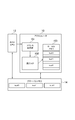
続いて図2を参照しながら、動的レジスタ配置及びスレッド・スケジューリングを行うアクセラレータ10を含むシステム構成例を説明する。
アクセラレータ10は、ホストCPU12及びグローバルメモリ14と共に情報処理システムを構成している。ホストCPU12は、データ処理を主として行う演算装置である。ホストCPU12は、OSをサポートしている。
グローバルメモリ14は、buf0、buf1、buf2の3つのメモリ領域を有している。グローバルメモリ14は、CPU12及びアクセラレータ10からのアクセスに応じて、データの読み込みや書き出しを行っている。
アクセラレータ10は、ホストCPU12の重い演算負荷に対処するために設けられている個別のマスタとして位置づけられている。アクセラレータ10は、アドレス変換部101と、実行コア102と、ローカルメモリ103とが設けられている。
アドレス変換部101は、処理実行部である実行コア102の処理の実行に対してアクセス先のアドレスを変換するアドレス変換処理を実行する部分である。アドレス変換部101は、処理実行部である実行コア102が処理に要するデータがローカルメモリ103に格納されていない場合に、処理実行部である実行コア102に対してグローバルメモリ14からローカルメモリ103にデータを移すようにアドレス変換処理を実行する。アドレス変換部101は、他の情報処理装置であるホストCPU12がグローバルメモリ14にアクセスする状況を監視し、グローバルメモリ14に必要とされるデータが無い場合に、処理実行部である実行コア102に対してローカルメモリ103からグローバルメモリ14にデータを移すようにアドレス変換処理を実行する。
実行コア102は、本開示の処理実行部に相当し、ローカルメモリ103及びグローバルメモリ14に格納されているデータに基づいて処理を実行する部分である。
ローカルメモリ103は、buf0、buf1、buf2の3つのメモリ領域を有している。ローカルメモリ103は、実行コア102からのアクセスのみを受け付けて、データの読み込みや書き出しを行っている。
上記したように本実施形態に係るアクセラレータ10は、本開示の情報処理装置であって、自身が専有するローカルメモリ103と他の情報処理装置であるホストCPU12と共有するグローバルメモリ14との双方にアクセス可能なものであって、ローカルメモリ及び前記グローバルメモリに格納されているデータに基づいて処理を実行する処理実行部である実行コア102と、処理実行部である実行コア102の処理の実行に対してアクセス先のアドレスを変換するアドレス変換処理を実行するアドレス変換部101と、を備えるものである。
続いて、アクセラレータ10の処理について、図3、図4、図5、図6を参照しながら説明する。図3は、説明に用いるためのプログラムのグラフ構造を例示する図である。図3に示される例では、buf0に格納されているデータを用いてGraph1の処理を実行し、結果をbuf1に格納する。続いて、buf1に格納されているデータを用いてGraph2の処理を実行し、結果をbuf2に格納する。このような処理を前提として説明を続ける。
図4は、図3に示されるような処理を実行する際のシーケンス図である。図5は、図4に示されるような処理を行った場合のグローバルメモリ14及びローカルメモリ103の状況を示す図である。
図4に示されるように、ホストCPU12から、アクセラレータ10に対してGraph1の実行が指示される(ステップS001)。図5(A)に示されるように、この時点では、ローカルメモリ103にはデータが格納されておらず、グローバルメモリ14のbuf0にdata001が格納されている。
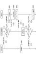
ステップS001の実行指示に応じて、アドレス変換部101は、ローカルメモリ103にbuf0のデータが格納されているか否かを判断する(ステップS101)。ローカルメモリ103にbuf0のデータが格納されていれば、ステップS104の処理に進む。ローカルメモリ103にbuf0のデータが格納されていなければ、ステップS102の処理に進む。
図5(A)に示されるように、この時点では、ローカルメモリ103にはデータが格納されていない場合、ステップS102の処理を実行する。ステップS102では、アドレス変換部101が、実行コア102に対して、グローバルメモリ14からbuf0のデータを読み込んで、ローカルメモリ103に書き込む指示を出力する。
この指示に応じて、実行コア102は、buf0のデータをグローバルメモリ14から読み込んで、ローカルメモリ103に書き込む(ステップS201)。図5(B)に示されるように、ローカルメモリ103のbuf0にもdata001が格納される。
続いて、アドレス変換部101から実行コア102に、Graph1の実行指示が出力される(ステップS103)。この指示に応じて、実行コア102は、Graph1の処理を実行する(ステップS202)。実行コア102は、実行結果をbuf1に書き込む(ステップS203)。この書き込みの結果、図5(C)に示されるように、ローカルメモリ103のbuf1にdata002が格納される。
実行コア102からホストCPU12に、Graph1の完了通知が送信される(ステップS204)。この段階では、図5(C)に示されるように、グローバルメモリ14のbuf1にはデータが書き込まれていない。
アドレス変換部101は、ホストCPU12のメモリアクセス状況をモニタリングする(ステップS104)。ホストCPU12は、ステップS204の通知によってGraph1が完了していることを認識しているので、Graph1の実行結果であるbuf1をグローバルメモリ14から読み込んで次の処理を行う場合がある(ステップS002)。
アドレス変換部101は、ステップS002におけるCPU12の処理を検知し、グローバルメモリ14にbuf1が格納されているか否かを判断する(ステップS105)。グローバルメモリ14にbuf1が格納されていれば、特段のアクションは起こさない。グローバルメモリ14にbuf1が格納されていない場合、CPU12に読込遅延処理を行う(ステップS107)。この処理は、後述する実行コア102の処理が終了するまでCPU12がグローバルメモリ14からデータを読み込む処理を遅延させるものである。
アドレス変換部101は、実行コア102にbuf1をローカルメモリ103からグローバルメモリ14に書き込む指示を出力する(ステップS106)。この指示に応じて、実行コア102は、ローカルメモリ103のbuf1をグローバルメモリ14に書き込む処理を実行する(ステップS205)。この書き込みの結果、図5(D)に示されるように、グローバルメモリ14のbuf1にdata002が格納される。
このような必要に応じた場合のみのローカルメモリ103からグローバルメモリ14への書き込みは、Graph2まで処理が進む場合も実行される。図6は、その場合のローカルメモリ103及びグローバルメモリ14のデータ書き込み状況を示すものである。
図6(A)及び図6(B)は、図5(A)図5(B)と同じ状況となっている。ここで、CPU12からGraph2の実行が指示されると、実行コア102はGraph2を実行することになり、結果であるbuf2のdata003をローカルメモリ103にのみ書き込む。
CPU12は通知によってGraph2が完了していることを認識しているので、Graph2の実行結果であるbuf2をグローバルメモリ14から読み込んで次の処理を行う場合がある。このアクションをアドレス変換部101が認識し、実行コア102は、ローカルメモリ103からグローバルメモリ14にbuf2の書き込みを行う。図6(D)に示されるように、CPU12が必要としなかったbuf1はグローバルメモリ14へ掻き出されないので、メモリの無駄なアクセスを低減することができる。
比較のため、アドレス変換を行わない場合の例について、図7及び図8を参照しながら説明する。図7に示されるように、ホストCPUから、アクセラレータに対してGraph1の実行が指示される(ステップS051)。図8(A)に示されるように、この時点では、ローカルメモリにはデータが格納されておらず、グローバルメモリのbuf0にdata001が格納されている。
実行コアは、グローバルメモリからbuf0を読み込んで、ローカルメモリに書き込む(ステップS251)。この段階で、図8(B)に示されるように、ローカルメモリのbuf1にデータが書き込まれる。
実行コアは、Graph1を実行する(ステップS252)。実行コアは、Graph1の実行結果であるbuf1をローカルメモリに書き込む(ステップS253)。実行コアは、buf1をグローバルメモリに書き込む(ステップS254)。この段階で、図8(C)に示されるように、グローバルメモリのbuf1にデータが書き込まれる。
実行コアは、Graph1の完了通知をホストCPUに送信する(ステップS255)。ホストCPUは、グローバルメモリからbuf1を読み込む(ステップS052)。
実行コアがGraph2を実行すると、実行完了時に即座にグローバルメモリにもbuf2が書き込まれ、図8(D)の状態となる。
本実施形態のメモリ書き込み例である図6と、比較例のメモリ書き込み例である図8とを比較すると明らかなように、本実施形態では必要な場合のみにローカルメモリ103からグローバルメモリ14への書き込みが行われるので、より処理を高速化することができる。
以上、具体例を参照しつつ本実施形態について説明した。しかし、本開示はこれらの具体例に限定されるものではない。これら具体例に、当業者が適宜設計変更を加えたものも、本開示の特徴を備えている限り、本開示の範囲に包含される。前述した各具体例が備える各要素およびその配置、条件、形状などは、例示したものに限定されるわけではなく適宜変更することができる。前述した各具体例が備える各要素は、技術的な矛盾が生じない限り、適宜組み合わせを変えることができる。
Claims (3)
- 自身が専有するローカルメモリと他の情報処理装置と共有するグローバルメモリとの双方にアクセス可能な情報処理装置であって、
前記ローカルメモリ及び前記グローバルメモリに格納されているデータに基づいて処理を実行する処理実行部(102)と、
前記処理実行部の処理の実行に対してアクセス先のアドレスを変換するアドレス変換処理を実行するアドレス変換部(101)と、を備える情報処理装置。 - 請求項1に記載の情報処理装置であって、
前記アドレス変換部は、前記処理実行部が処理に要するデータが前記ローカルメモリに格納されていない場合に、前記処理実行部に対して前記グローバルメモリから前記ローカルメモリにデータを移すように前記アドレス変換処理を実行する、情報処理装置。 - 請求項2に記載の情報処理装置であって、
前記アドレス変換部は、他の情報処理装置が前記グローバルメモリにアクセスする状況を監視し、前記グローバルメモリに必要とされるデータが無い場合に、前記処理実行部に対して前記ローカルメモリから前記グローバルメモリにデータを移すように前記アドレス変換処理を実行する、情報処理装置。
Applications Claiming Priority (2)
| Application Number | Priority Date | Filing Date | Title |
|---|---|---|---|
| JP2018068428A JP7080698B2 (ja) | 2018-03-30 | 2018-03-30 | 情報処理装置 |
| JP2018-068428 | 2018-03-30 |
Publications (1)
| Publication Number | Publication Date |
|---|---|
| WO2019188174A1 true WO2019188174A1 (ja) | 2019-10-03 |
Family
ID=68058896
Family Applications (1)
| Application Number | Title | Priority Date | Filing Date |
|---|---|---|---|
| PCT/JP2019/009626 Ceased WO2019188174A1 (ja) | 2018-03-30 | 2019-03-11 | 情報処理装置 |
Country Status (2)
| Country | Link |
|---|---|
| JP (1) | JP7080698B2 (ja) |
| WO (1) | WO2019188174A1 (ja) |
Families Citing this family (1)
| Publication number | Priority date | Publication date | Assignee | Title |
|---|---|---|---|---|
| US12056382B2 (en) * | 2020-05-26 | 2024-08-06 | Qualcomm Incorporated | Inference in memory |
Citations (1)
| Publication number | Priority date | Publication date | Assignee | Title |
|---|---|---|---|---|
| JP2011070253A (ja) * | 2009-09-24 | 2011-04-07 | Mitsubishi Electric Corp | メモリ制御システム |
Family Cites Families (1)
| Publication number | Priority date | Publication date | Assignee | Title |
|---|---|---|---|---|
| US8941655B2 (en) * | 2011-09-07 | 2015-01-27 | Qualcomm Incorporated | Memory copy engine for graphics processing |
-
2018
- 2018-03-30 JP JP2018068428A patent/JP7080698B2/ja active Active
-
2019
- 2019-03-11 WO PCT/JP2019/009626 patent/WO2019188174A1/ja not_active Ceased
Patent Citations (1)
| Publication number | Priority date | Publication date | Assignee | Title |
|---|---|---|---|---|
| JP2011070253A (ja) * | 2009-09-24 | 2011-04-07 | Mitsubishi Electric Corp | メモリ制御システム |
Also Published As
| Publication number | Publication date |
|---|---|
| JP2019179411A (ja) | 2019-10-17 |
| JP7080698B2 (ja) | 2022-06-06 |
Similar Documents
| Publication | Publication Date | Title |
|---|---|---|
| US8478926B1 (en) | Co-processing acceleration method, apparatus, and system | |
| CN108647104B (zh) | 请求处理方法、服务器及计算机可读存储介质 | |
| CN113918101B (zh) | 一种写数据高速缓存的方法、系统、设备和存储介质 | |
| KR20090066765A (ko) | 멀티코어 플랫폼에서의 태스크 이동 방법 및 장치 | |
| JP2009265963A (ja) | 情報処理システム及びタスクの実行制御方法 | |
| CN105159841B (zh) | 一种内存迁移方法及装置 | |
| JP6880402B2 (ja) | メモリアクセス制御装置及びその制御方法 | |
| WO2017056725A1 (ja) | 車載制御装置 | |
| JP4381459B1 (ja) | 情報処理装置、粒度調整方法およびプログラム | |
| CN118860925A (zh) | Dma引擎控制器及其控制方法、电子设备及存储介质 | |
| CN120104043A (zh) | 一种数据处理方法、装置和计算设备 | |
| JP2007207026A (ja) | Dma転送装置 | |
| JP2015158894A (ja) | 画像形成装置、画像形成処理用データ転送制御方法、及び画像形成処理用データ転送制御プログラム | |
| WO2019188174A1 (ja) | 情報処理装置 | |
| US9311225B2 (en) | DMA channels | |
| US10289329B2 (en) | Burst buffer dynamic logical volume sizing in high performance computing environment | |
| JP6817827B2 (ja) | アクセラレータ処理管理装置、ホスト装置、アクセラレータ処理実行システム、方法およびプログラム | |
| US20110191638A1 (en) | Parallel computer system and method for controlling parallel computer system | |
| JP2008065478A (ja) | 情報処理装置、データ転送方法及びプログラム | |
| JP2010231295A (ja) | 解析システム | |
| JP2008210280A (ja) | 半導体装置及びdmaコントローラ | |
| JP7064367B2 (ja) | デッドロック回避方法、デッドロック回避装置 | |
| WO2013128531A1 (ja) | 計算機システム、その処理方法、及びコンピュータ可読媒体 | |
| JP2009193260A (ja) | ストレージシステム、ストレージ装置、優先度制御装置および優先度制御方法 | |
| JP5561147B2 (ja) | 仮想記憶管理装置、仮想記憶管理方法および仮想記憶管理プログラム |
Legal Events
| Date | Code | Title | Description |
|---|---|---|---|
| 121 | Ep: the epo has been informed by wipo that ep was designated in this application |
Ref document number: 19778409 Country of ref document: EP Kind code of ref document: A1 |
|
| 122 | Ep: pct application non-entry in european phase |
Ref document number: 19778409 Country of ref document: EP Kind code of ref document: A1 |