WO2019187583A1 - Semiconductor light emitting element - Google Patents
Semiconductor light emitting element Download PDFInfo
- Publication number
- WO2019187583A1 WO2019187583A1 PCT/JP2019/002749 JP2019002749W WO2019187583A1 WO 2019187583 A1 WO2019187583 A1 WO 2019187583A1 JP 2019002749 W JP2019002749 W JP 2019002749W WO 2019187583 A1 WO2019187583 A1 WO 2019187583A1
- Authority
- WO
- WIPO (PCT)
- Prior art keywords
- layer
- region
- composition ratio
- barrier layer
- semiconductor
- Prior art date
Links
Images


Classifications
-
- H—ELECTRICITY
- H01—ELECTRIC ELEMENTS
- H01S—DEVICES USING THE PROCESS OF LIGHT AMPLIFICATION BY STIMULATED EMISSION OF RADIATION [LASER] TO AMPLIFY OR GENERATE LIGHT; DEVICES USING STIMULATED EMISSION OF ELECTROMAGNETIC RADIATION IN WAVE RANGES OTHER THAN OPTICAL
- H01S5/00—Semiconductor lasers
- H01S5/30—Structure or shape of the active region; Materials used for the active region
- H01S5/34—Structure or shape of the active region; Materials used for the active region comprising quantum well or superlattice structures, e.g. single quantum well [SQW] lasers, multiple quantum well [MQW] lasers or graded index separate confinement heterostructure [GRINSCH] lasers
- H01S5/343—Structure or shape of the active region; Materials used for the active region comprising quantum well or superlattice structures, e.g. single quantum well [SQW] lasers, multiple quantum well [MQW] lasers or graded index separate confinement heterostructure [GRINSCH] lasers in AIIIBV compounds, e.g. AlGaAs-laser, InP-based laser
- H01S5/34333—Structure or shape of the active region; Materials used for the active region comprising quantum well or superlattice structures, e.g. single quantum well [SQW] lasers, multiple quantum well [MQW] lasers or graded index separate confinement heterostructure [GRINSCH] lasers in AIIIBV compounds, e.g. AlGaAs-laser, InP-based laser with a well layer based on Ga(In)N or Ga(In)P, e.g. blue laser
-
- H—ELECTRICITY
- H01—ELECTRIC ELEMENTS
- H01S—DEVICES USING THE PROCESS OF LIGHT AMPLIFICATION BY STIMULATED EMISSION OF RADIATION [LASER] TO AMPLIFY OR GENERATE LIGHT; DEVICES USING STIMULATED EMISSION OF ELECTROMAGNETIC RADIATION IN WAVE RANGES OTHER THAN OPTICAL
- H01S5/00—Semiconductor lasers
- H01S5/20—Structure or shape of the semiconductor body to guide the optical wave ; Confining structures perpendicular to the optical axis, e.g. index or gain guiding, stripe geometry, broad area lasers, gain tailoring, transverse or lateral reflectors, special cladding structures, MQW barrier reflection layers
- H01S5/2004—Confining in the direction perpendicular to the layer structure
- H01S5/2009—Confining in the direction perpendicular to the layer structure by using electron barrier layers
-
- H—ELECTRICITY
- H01—ELECTRIC ELEMENTS
- H01L—SEMICONDUCTOR DEVICES NOT COVERED BY CLASS H10
- H01L33/00—Semiconductor devices with at least one potential-jump barrier or surface barrier specially adapted for light emission; Processes or apparatus specially adapted for the manufacture or treatment thereof or of parts thereof; Details thereof
- H01L33/0004—Devices characterised by their operation
- H01L33/0045—Devices characterised by their operation the devices being superluminescent diodes
-
- H—ELECTRICITY
- H01—ELECTRIC ELEMENTS
- H01S—DEVICES USING THE PROCESS OF LIGHT AMPLIFICATION BY STIMULATED EMISSION OF RADIATION [LASER] TO AMPLIFY OR GENERATE LIGHT; DEVICES USING STIMULATED EMISSION OF ELECTROMAGNETIC RADIATION IN WAVE RANGES OTHER THAN OPTICAL
- H01S5/00—Semiconductor lasers
- H01S5/20—Structure or shape of the semiconductor body to guide the optical wave ; Confining structures perpendicular to the optical axis, e.g. index or gain guiding, stripe geometry, broad area lasers, gain tailoring, transverse or lateral reflectors, special cladding structures, MQW barrier reflection layers
- H01S5/2004—Confining in the direction perpendicular to the layer structure
- H01S5/2018—Optical confinement, e.g. absorbing-, reflecting- or waveguide-layers
- H01S5/2031—Optical confinement, e.g. absorbing-, reflecting- or waveguide-layers characterized by special waveguide layers, e.g. asymmetric waveguide layers or defined bandgap discontinuities
-
- H—ELECTRICITY
- H01—ELECTRIC ELEMENTS
- H01S—DEVICES USING THE PROCESS OF LIGHT AMPLIFICATION BY STIMULATED EMISSION OF RADIATION [LASER] TO AMPLIFY OR GENERATE LIGHT; DEVICES USING STIMULATED EMISSION OF ELECTROMAGNETIC RADIATION IN WAVE RANGES OTHER THAN OPTICAL
- H01S5/00—Semiconductor lasers
- H01S5/20—Structure or shape of the semiconductor body to guide the optical wave ; Confining structures perpendicular to the optical axis, e.g. index or gain guiding, stripe geometry, broad area lasers, gain tailoring, transverse or lateral reflectors, special cladding structures, MQW barrier reflection layers
- H01S5/22—Structure or shape of the semiconductor body to guide the optical wave ; Confining structures perpendicular to the optical axis, e.g. index or gain guiding, stripe geometry, broad area lasers, gain tailoring, transverse or lateral reflectors, special cladding structures, MQW barrier reflection layers having a ridge or stripe structure
-
- H—ELECTRICITY
- H01—ELECTRIC ELEMENTS
- H01S—DEVICES USING THE PROCESS OF LIGHT AMPLIFICATION BY STIMULATED EMISSION OF RADIATION [LASER] TO AMPLIFY OR GENERATE LIGHT; DEVICES USING STIMULATED EMISSION OF ELECTROMAGNETIC RADIATION IN WAVE RANGES OTHER THAN OPTICAL
- H01S5/00—Semiconductor lasers
- H01S5/30—Structure or shape of the active region; Materials used for the active region
- H01S5/34—Structure or shape of the active region; Materials used for the active region comprising quantum well or superlattice structures, e.g. single quantum well [SQW] lasers, multiple quantum well [MQW] lasers or graded index separate confinement heterostructure [GRINSCH] lasers
- H01S5/3407—Structure or shape of the active region; Materials used for the active region comprising quantum well or superlattice structures, e.g. single quantum well [SQW] lasers, multiple quantum well [MQW] lasers or graded index separate confinement heterostructure [GRINSCH] lasers characterised by special barrier layers
-
- H—ELECTRICITY
- H01—ELECTRIC ELEMENTS
- H01L—SEMICONDUCTOR DEVICES NOT COVERED BY CLASS H10
- H01L33/00—Semiconductor devices with at least one potential-jump barrier or surface barrier specially adapted for light emission; Processes or apparatus specially adapted for the manufacture or treatment thereof or of parts thereof; Details thereof
- H01L33/02—Semiconductor devices with at least one potential-jump barrier or surface barrier specially adapted for light emission; Processes or apparatus specially adapted for the manufacture or treatment thereof or of parts thereof; Details thereof characterised by the semiconductor bodies
- H01L33/14—Semiconductor devices with at least one potential-jump barrier or surface barrier specially adapted for light emission; Processes or apparatus specially adapted for the manufacture or treatment thereof or of parts thereof; Details thereof characterised by the semiconductor bodies with a carrier transport control structure, e.g. highly-doped semiconductor layer or current-blocking structure
-
- H—ELECTRICITY
- H01—ELECTRIC ELEMENTS
- H01L—SEMICONDUCTOR DEVICES NOT COVERED BY CLASS H10
- H01L33/00—Semiconductor devices with at least one potential-jump barrier or surface barrier specially adapted for light emission; Processes or apparatus specially adapted for the manufacture or treatment thereof or of parts thereof; Details thereof
- H01L33/02—Semiconductor devices with at least one potential-jump barrier or surface barrier specially adapted for light emission; Processes or apparatus specially adapted for the manufacture or treatment thereof or of parts thereof; Details thereof characterised by the semiconductor bodies
- H01L33/26—Materials of the light emitting region
- H01L33/30—Materials of the light emitting region containing only elements of group III and group V of the periodic system
- H01L33/32—Materials of the light emitting region containing only elements of group III and group V of the periodic system containing nitrogen
-
- H—ELECTRICITY
- H01—ELECTRIC ELEMENTS
- H01S—DEVICES USING THE PROCESS OF LIGHT AMPLIFICATION BY STIMULATED EMISSION OF RADIATION [LASER] TO AMPLIFY OR GENERATE LIGHT; DEVICES USING STIMULATED EMISSION OF ELECTROMAGNETIC RADIATION IN WAVE RANGES OTHER THAN OPTICAL
- H01S5/00—Semiconductor lasers
- H01S5/005—Optical components external to the laser cavity, specially adapted therefor, e.g. for homogenisation or merging of the beams or for manipulating laser pulses, e.g. pulse shaping
- H01S5/0087—Optical components external to the laser cavity, specially adapted therefor, e.g. for homogenisation or merging of the beams or for manipulating laser pulses, e.g. pulse shaping for illuminating phosphorescent or fluorescent materials, e.g. using optical arrangements specifically adapted for guiding or shaping laser beams illuminating these materials
-
- H—ELECTRICITY
- H01—ELECTRIC ELEMENTS
- H01S—DEVICES USING THE PROCESS OF LIGHT AMPLIFICATION BY STIMULATED EMISSION OF RADIATION [LASER] TO AMPLIFY OR GENERATE LIGHT; DEVICES USING STIMULATED EMISSION OF ELECTROMAGNETIC RADIATION IN WAVE RANGES OTHER THAN OPTICAL
- H01S5/00—Semiconductor lasers
- H01S5/04—Processes or apparatus for excitation, e.g. pumping, e.g. by electron beams
- H01S5/042—Electrical excitation ; Circuits therefor
- H01S5/0425—Electrodes, e.g. characterised by the structure
- H01S5/04252—Electrodes, e.g. characterised by the structure characterised by the material
-
- H—ELECTRICITY
- H01—ELECTRIC ELEMENTS
- H01S—DEVICES USING THE PROCESS OF LIGHT AMPLIFICATION BY STIMULATED EMISSION OF RADIATION [LASER] TO AMPLIFY OR GENERATE LIGHT; DEVICES USING STIMULATED EMISSION OF ELECTROMAGNETIC RADIATION IN WAVE RANGES OTHER THAN OPTICAL
- H01S5/00—Semiconductor lasers
- H01S5/30—Structure or shape of the active region; Materials used for the active region
- H01S5/305—Structure or shape of the active region; Materials used for the active region characterised by the doping materials used in the laser structure
- H01S5/3077—Structure or shape of the active region; Materials used for the active region characterised by the doping materials used in the laser structure plane dependent doping
-
- H—ELECTRICITY
- H01—ELECTRIC ELEMENTS
- H01S—DEVICES USING THE PROCESS OF LIGHT AMPLIFICATION BY STIMULATED EMISSION OF RADIATION [LASER] TO AMPLIFY OR GENERATE LIGHT; DEVICES USING STIMULATED EMISSION OF ELECTROMAGNETIC RADIATION IN WAVE RANGES OTHER THAN OPTICAL
- H01S5/00—Semiconductor lasers
- H01S5/30—Structure or shape of the active region; Materials used for the active region
- H01S5/32—Structure or shape of the active region; Materials used for the active region comprising PN junctions, e.g. hetero- or double- heterostructures
- H01S5/323—Structure or shape of the active region; Materials used for the active region comprising PN junctions, e.g. hetero- or double- heterostructures in AIIIBV compounds, e.g. AlGaAs-laser, InP-based laser
- H01S5/32308—Structure or shape of the active region; Materials used for the active region comprising PN junctions, e.g. hetero- or double- heterostructures in AIIIBV compounds, e.g. AlGaAs-laser, InP-based laser emitting light at a wavelength less than 900 nm
- H01S5/32341—Structure or shape of the active region; Materials used for the active region comprising PN junctions, e.g. hetero- or double- heterostructures in AIIIBV compounds, e.g. AlGaAs-laser, InP-based laser emitting light at a wavelength less than 900 nm blue laser based on GaN or GaP
-
- H—ELECTRICITY
- H01—ELECTRIC ELEMENTS
- H01S—DEVICES USING THE PROCESS OF LIGHT AMPLIFICATION BY STIMULATED EMISSION OF RADIATION [LASER] TO AMPLIFY OR GENERATE LIGHT; DEVICES USING STIMULATED EMISSION OF ELECTROMAGNETIC RADIATION IN WAVE RANGES OTHER THAN OPTICAL
- H01S5/00—Semiconductor lasers
- H01S5/30—Structure or shape of the active region; Materials used for the active region
- H01S5/34—Structure or shape of the active region; Materials used for the active region comprising quantum well or superlattice structures, e.g. single quantum well [SQW] lasers, multiple quantum well [MQW] lasers or graded index separate confinement heterostructure [GRINSCH] lasers
- H01S5/343—Structure or shape of the active region; Materials used for the active region comprising quantum well or superlattice structures, e.g. single quantum well [SQW] lasers, multiple quantum well [MQW] lasers or graded index separate confinement heterostructure [GRINSCH] lasers in AIIIBV compounds, e.g. AlGaAs-laser, InP-based laser
- H01S5/34346—Structure or shape of the active region; Materials used for the active region comprising quantum well or superlattice structures, e.g. single quantum well [SQW] lasers, multiple quantum well [MQW] lasers or graded index separate confinement heterostructure [GRINSCH] lasers in AIIIBV compounds, e.g. AlGaAs-laser, InP-based laser characterised by the materials of the barrier layers
Definitions
- the present disclosure relates to a semiconductor light emitting device.
- an in-vehicle laser headlight light source with increased brightness by using a semiconductor laser element having a higher emission intensity than an LED as a light source has attracted attention.
- an ultra-high-power blue semiconductor laser element capable of operating for a long period of several thousand hours or more even when a watt-class high-power operation is performed at a high temperature of 85 ° C. Is desired.
- the phosphor can be excited with such an ultra-high output blue laser light to obtain yellow light, a white ultra-high output light source as a whole can be obtained.
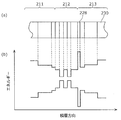
- FIG. 33 is a schematic diagram showing the layer structure of the semiconductor light emitting device disclosed in Patent Document 1.
- a structural diagram (a) and a graph (b) in FIG. 33 respectively show a stacked structure and a band structure of a semiconductor light emitting device disclosed in Patent Document 1.
- an active layer 212 is sandwiched between an n-type layer 211 and a p-type layer 213.
- a p-side electron confinement layer 228 corresponding to an electron barrier layer having a band gap energy higher than that of the upper cladding layer 230 is disposed between the active layer 212 and the upper cladding layer 230. According to this structure, even during high-temperature operation, electrons injected into the active layer 212 are unlikely to leak into the upper cladding layer 230 due to the energy barrier of the p-side electron confinement layer 228 made of AlGaN.
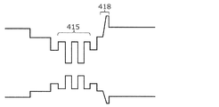
- FIG. 34 is a schematic diagram showing a bandgap energy distribution of the semiconductor light emitting device disclosed in Patent Document 2.
- the Al composition ratio is gradually changed at the interface of the electron barrier layer 418 made of AlGaN on the active layer 415 side.
- the polarization electric field formed at the interface is dispersed in the region where the Al composition ratio is changed, and the change in the band structure due to the polarization electric field of the electron barrier layer 418 is reduced, thereby reducing the operating voltage. Yes.
- the Al composition ratio on the n-type cladding layer side of the electron barrier layer is gradually increased from the active layer side to the p-type cladding layer side, the polarization electric field and the band gap can be gradually changed. It becomes possible.
- the change in the band structure of the valence band due to the polarization electric field and the change in the band gap energy can be offset, the increase in the energy barrier for the holes in the electron barrier layer is suppressed, and the energy barrier for the electrons is reduced. It can be increased.
- the present disclosure has been made to solve the above-described problems, and an object thereof is to provide a semiconductor light-emitting element with low power consumption even in high-temperature operation.
- a semiconductor light emitting device includes a GaN substrate, a first semiconductor layer that is disposed above the GaN substrate and includes a first conductivity type nitride-based semiconductor, and above the first semiconductor layer.
- a second semiconductor layer containing a nitride semiconductor of a second conductivity type different from the first conductivity type, and the electron barrier layer has an Al composition ratio in a stacking direction perpendicular to the main surface of the GaN substrate.
- a first region that changes at a first rate of change a second region that is disposed between the first region and the second semiconductor layer, and in which the Al composition ratio changes at a second rate of change in the stacking direction; In the first region and the second region. Te, Al composition ratio increases monotonically with respect to a direction toward the second semiconductor layer from the active layer, the second rate of change is greater than said first rate of change.
- the polarization charge surface density formed in the electron barrier layer increases from a linear change with a small inclination to a lamination direction from the active layer side with a linear change with a large inclination.
- the magnitude of the polarization charge is proportional to the rate of change of the polarization charge surface density, a positive polarization charge whose magnitude increases in two steps from the active layer side to the stacking direction is formed in the electron barrier layer. Is done.
- the positive polarization charge surface density generated at the active layer side interface of the electron barrier layer decreases. At this time, electrons are attracted to the interface on the active layer side in order to satisfy the electrical neutral condition. However, since the positive polarization charge density in the vicinity of the active layer in the electron barrier layer is small, this interface is As a result, the electron concentration induced electrically is also reduced.
- the decrease in the band potential due to the influence of electrons generated at the active layer side interface of the electron barrier layer is suppressed, the potential barrier for holes formed in the valence band is reduced, and the electrons formed in the conduction band are reduced.
- the potential barrier increases.
- FIG. 1A is a schematic cross-sectional view showing a schematic configuration of a semiconductor light emitting element according to Embodiment 1.
- FIG. 1B is a graph showing a conduction band energy distribution with respect to the stacking direction of the active layers according to Embodiment 1.
- FIG. 2 is a schematic diagram showing the configuration of the electron barrier layer of the semiconductor light emitting device according to Comparative Example 1.
- FIG. 3 is a schematic diagram showing the configuration of the electron barrier layer of the semiconductor light emitting device according to the first embodiment.
- 4A is a schematic diagram showing a first example of a band gap energy distribution in the stacking direction of the electron barrier layer of the semiconductor light emitting device according to Embodiment 1.
- FIG. 1A is a schematic cross-sectional view showing a schematic configuration of a semiconductor light emitting element according to Embodiment 1.
- FIG. 1B is a graph showing a conduction band energy distribution with respect to the stacking direction of the active layers according to Embodiment 1.
- FIG. 2 is
- FIG. 4B is a schematic diagram illustrating a second example of a band gap energy distribution in the stacking direction of the electron barrier layer of the semiconductor light emitting device according to Embodiment 1.
- FIG. 5A is a schematic diagram illustrating a third example of a band gap energy distribution in the stacking direction of the electron barrier layer of the semiconductor light emitting element according to Embodiment 1.
- FIG. 5B is a schematic diagram illustrating a fourth example of a band gap energy distribution in the stacking direction of the electron barrier layer of the semiconductor light emitting element according to Embodiment 1.
- FIG. 5C is a schematic diagram illustrating a fifth example of the band gap energy distribution in the stacking direction of the electron barrier layer of the semiconductor light emitting device according to Embodiment 1.
- FIG. 5D is a schematic diagram illustrating a sixth example of the band gap energy distribution in the stacking direction of the electron barrier layers of the semiconductor light emitting element according to Embodiment 1.
- FIG. 6 is a diagram illustrating an example of an Al composition ratio distribution in the stacking direction of the electron barrier layer according to the first embodiment.
- FIG. 7 is a diagram illustrating another example of the Al composition ratio distribution in the stacking direction of the electron barrier layer according to the first embodiment.
- FIG. 8 is a diagram illustrating a simulation result of the first configuration example of the semiconductor light emitting element according to the first embodiment.
- FIG. 9 is a diagram illustrating simulation results of the semiconductor light emitting element according to Comparative Example 2.
- FIG. 10 is a diagram illustrating a simulation result of the second configuration example of the semiconductor light emitting element according to the first embodiment.
- FIG. 11 is a diagram illustrating a simulation result of the third configuration example of the semiconductor light emitting element according to the first embodiment.
- FIG. 12 is a diagram illustrating a simulation result of the semiconductor light emitting element according to Comparative Example 3.
- FIG. 13 is a schematic diagram showing the Al composition ratio distribution shape of the electron barrier layer used in the simulation.
- FIG. 14 is a graph showing a simulation result when the thickness of the electron barrier layer is 5 nm.
- FIG. 15 is a graph showing a simulation result when the thickness of the electron barrier layer is 15 nm.
- FIG. 14 is a graph showing a simulation result when the thickness of the electron barrier layer is 5 nm.
- FIG. 16 is a schematic diagram showing an impurity doping profile of the second semiconductor layer in the semiconductor light emitting device according to the first embodiment.
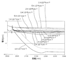
- FIG. 17A is a graph showing the dependency of the operating voltage on the impurity concentration in the low impurity concentration region in the semiconductor light emitting device according to the first embodiment.
- FIG. 17B is a graph showing the dependency of waveguide loss on the impurity concentration in the low impurity concentration region in the semiconductor light emitting device according to Embodiment 1.
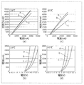
- FIG. 18 shows the valence band structure and hole Fermi level when the impurity doping concentration in the low impurity concentration region according to the first embodiment is changed from 1 ⁇ 10 17 cm ⁇ 3 to 1 ⁇ 10 19 cm ⁇ 3. It is a graph which shows the calculation result of.
- FIG. 18 shows the valence band structure and hole Fermi level when the impurity doping concentration in the low impurity concentration region according to the first embodiment is changed from 1 ⁇ 10 17 cm ⁇ 3 to 1 ⁇ 10 19 cm
- FIG. 19 is a graph showing the characteristics of the semiconductor light emitting device when the Al composition ratio distribution shape of the electron barrier layer is set to the shape a, the shape b, and the shape c.
- FIG. 20 is a schematic diagram illustrating the formation of polarization charges in the composition ratio gradient region of the third light guide layer of the semiconductor light emitting device according to the second embodiment.
- FIG. 21 is a schematic diagram illustrating the formation of polarization charges in the third light guide layer of the semiconductor light emitting element according to Comparative Example 4.
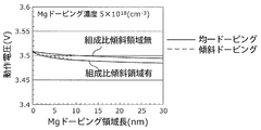
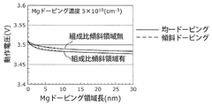
- FIG. 22A shows the Mg doping of the operating voltage of the semiconductor light emitting device according to the second embodiment when the Mg doping concentration is 5 ⁇ 10 18 cm ⁇ 3 , 1 ⁇ 10 19 cm ⁇ 3 and 2 ⁇ 10 19 cm ⁇ 3.
- FIG. 22B shows the Mg doping of the operating voltage of the semiconductor light emitting device according to the second embodiment when the Mg doping concentration is 5 ⁇ 10 18 cm ⁇ 3 , 1 ⁇ 10 19 cm ⁇ 3 and 2 ⁇ 10 19 cm ⁇ 3. It is a graph which shows area
- FIG. 22C shows the Mg doping of the operating voltage of the semiconductor light emitting device according to the second embodiment when the Mg doping concentration is 5 ⁇ 10 18 cm ⁇ 3 , 1 ⁇ 10 19 cm ⁇ 3 and 2 ⁇ 10 19 cm ⁇ 3. It is a graph which shows area
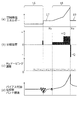
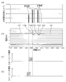
- FIG. 23 is a schematic diagram showing an aspect of impurity doping according to the second embodiment.
- FIG. 24 is a graph showing a conduction band structure and a valence band structure when the barrier layer is Si-doped in the semiconductor light emitting device according to the second embodiment.
- FIG. 25 is a graph showing a conduction band structure and a valence band structure in the case where Si is doped at the interface between the barrier layer and the second light guide layer in the semiconductor light emitting device according to the second embodiment.
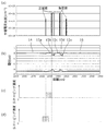
- FIG. 26 is a schematic diagram showing an aspect of impurity doping according to the third embodiment.
- FIG. 27 is a graph showing a conduction band structure and a valence band structure when the barrier layer is Si-doped in the semiconductor light emitting device according to the third embodiment.
- FIG. 28 is a graph showing a conduction band structure and a valence band structure when Si doping is performed on the interface between the barrier layer and the second light guide layer in the semiconductor light emitting device according to the third embodiment.
- FIG. 29 is a schematic diagram showing the relationship between the impurity doping profile of the semiconductor light emitting device according to the fourth embodiment and the forbidden band energy distribution.
- FIG. 30 is a graph showing the calculation result of the Al composition ratio dependency of the first semiconductor layer and the second semiconductor layer of the operating voltage during 300 mA operation in the semiconductor light emitting device according to the fourth embodiment.
- FIG. 31 is a schematic cross-sectional view showing a schematic configuration of the semiconductor light emitting element according to the fifth embodiment.
- FIG. 32 is a graph showing calculation results of the optical confinement coefficient and the effective refractive index difference of the semiconductor light emitting device according to the fifth embodiment.
- FIG. 33 is a schematic diagram showing the layer structure of the semiconductor light emitting device disclosed in Patent Document 1.
- FIG. 34 is a schematic diagram showing a bandgap energy distribution of the semiconductor light emitting device disclosed in Patent Document 2.
- the terms “upper” and “lower” do not refer to the upward direction (vertically upward) and the downward direction (vertically downward) in absolute space recognition, but are based on the stacking order in the stacking configuration. Is used as a term defined by the relative positional relationship. The terms “upper” and “lower” are used not only when two components are spaced apart from each other and there is another component between the two components. This is also applied to the case where they are arranged in contact with each other.
- FIG. 1A is a schematic cross-sectional view showing a schematic configuration of a semiconductor light emitting device 100 according to the present embodiment.
- the semiconductor light emitting device 100 is a nitride-based semiconductor laser device.
- FIG. 1A shows a cross section perpendicular to the resonance direction of the semiconductor light emitting device 100.
- the semiconductor light emitting device 100 includes a GaN substrate 11, a first semiconductor layer 12, an active layer 15, an electron barrier layer 18, and a second semiconductor layer 19.
- the semiconductor light emitting device 100 further includes a first light guide layer 13, a second light guide layer 14, a third light guide layer 16, an intermediate layer 17, a contact layer 20, and a current block.
- a layer 30, an n-side electrode 31, and a p-side electrode 32 are provided.
- the first semiconductor layer 12 is a layer that is disposed above the GaN substrate 11 and includes a nitride semiconductor of the first conductivity type.
- the first conductivity type is n-type.
- the first semiconductor layer 12 is an n-type AlGaN layer having a thickness of 1.5 ⁇ m.
- the first light guide layer 13 is a first conductivity type semiconductor layer which is disposed above the first semiconductor layer 12 and made of n-type GaN having a thickness of 100 nm.
- the second light guide layer 14 is disposed above the first light guide layer 13 and is a layer made of InGaN having a thickness of 185 nm.
- the active layer 15 is a layer that is disposed above the first semiconductor layer 12 and includes a nitride-based semiconductor containing Ga or In. In the present embodiment, the active layer 15 is disposed above the second light guide layer 14 and includes an undoped multiple quantum well.
- the third light guide layer 16 is disposed above the active layer 15 and is a layer made of InGaN having a thickness of 90 nm.
- the intermediate layer 17 is a layer that is disposed between the electron barrier layer 18 and the active layer 15 and includes a nitride-based semiconductor.
- the intermediate layer 17 is disposed between the electron barrier layer 18 and the third light guide layer 16 and includes the second conductivity type GaN having a thickness of 3 nm.
- the second conductivity type is a conductivity type different from the first conductivity type, and is p-type in the present embodiment.
- the electron barrier layer 18 is a second conductivity type layer that is disposed above the active layer 15 and includes a nitride-based semiconductor containing at least Al.
- the electron barrier layer 18 is disposed between the intermediate layer 17 and the second semiconductor layer 19 and is made of p-type AlGaN.
- the second semiconductor layer 19 is a semiconductor layer of the second conductivity type that is disposed above the electron barrier layer 18 and includes a nitride semiconductor of the second conductivity type.
- the second semiconductor layer 19 is a p-type AlGaN cladding layer having a thickness of 660 nm.
- the contact layer 20 is a layer that is disposed above the second semiconductor layer 19 and includes a nitride semiconductor of the second conductivity type.
- the contact layer 20 is made of p-type GaN having a thickness of 0.05 ⁇ m.
- the current blocking layer 30 is an insulating layer that is disposed above the second semiconductor layer 19 and is transmissive to the light from the active layer 15.
- the current blocking layer 30 is made of SiO 2.
- the n-side electrode 31 is a conductive layer disposed below the GaN substrate 11.
- the n-side electrode 31 is, for example, a single layer film or a multilayer film formed of at least one of Cr, Ti, Ni, Pd, Pt, and Au.
- the p-side electrode 32 is a conductive layer disposed above the contact layer 20. In the present embodiment, the p-side electrode 32 is disposed above the contact layer 20 and the current blocking layer 30.
- the p-side electrode 32 is, for example, a single layer film or a multilayer film formed of at least one of Cr, Ti, Ni, Pd, Pt, and Au.
- a ridge is formed in the second semiconductor layer 19 of the semiconductor light emitting device 100.
- the ridge width W is about 30 ⁇ m.
- the distance between the lower end of the ridge and the active layer is dp.
- the first semiconductor layer 12 in order to confine light in the vertical direction (substrate normal direction) to the active layer 15, the first semiconductor layer 12 made of an n-type AlGaN layer and the first semiconductor layer 12 made of a p-type AlGaN layer. 2
- the Al composition ratio of the semiconductor layer 19 is 0.035 (3.5%).
- the Al composition ratio of the first semiconductor layer 12 made of n-type AlGaN and the second semiconductor layer 19 made of p-type AlGaN layer is increased, the active layer 15, the first semiconductor layer 12 functioning as a cladding layer, and the second semiconductor layer 12
- the difference in refractive index with the semiconductor layer 19 can be increased.
- light can be strongly confined in the stacking direction of the active layer 15 (that is, the direction perpendicular to the main surface of the GaN substrate 11), and the oscillation threshold current value can be reduced.
- the Al composition ratio of the first semiconductor layer 12 and the second semiconductor layer 19 made of AlGaN is set to 0.05 (that is, 5%) or less.
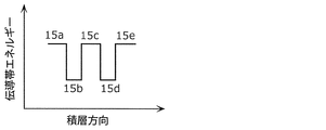
- FIG. 1B is a graph showing the conduction band energy distribution in the stacking direction of the active layer 15 according to the present embodiment.
- the active layer 15 has two well layers 15b and 15d made of InGaN having a film thickness of 3 nm and an In composition ratio of 0.16 (ie, 16%) in order to obtain laser oscillation with a wavelength of 450 nm. It has a DQW (Double Quantum Well) structure provided with.
- DQW Double Quantum Well
- the barrier layers 15a, 15c, and 15e are made of InGaN with a film thickness of 7 nm, a film thickness of 7 nm, and a film thickness of 5 nm, respectively, and an In composition ratio of 0.04 (that is, 4%).
- a high In composition ratio of 15% or more is required to obtain laser oscillation light in the 450 nm band.
- the lattice irregularity between the well layer and the GaN substrate 11 is 1.7% or more, and if the film thickness is excessively increased, lattice defects are generated.
- the thickness of the well layer is, for example, not less than 2.7 nm and not more than 3.3 nm.
- the second light guide layer 14 and the third light guide layer 16 include In and have a refractive index of the first semiconductor layer 12 made of n-type AlGaN and the second semiconductor layer 19 made of p-type AlGaN layer. It is also an enhanced layer. Thereby, the effective refractive index of the light distribution propagating through the waveguide corresponding to the ridge can be increased, and the confinement effect of the light distribution by the first semiconductor layer 12 and the second semiconductor layer 19 in the stacking direction can be increased.
- the In composition ratio of the second light guide layer 14 and the third light guide layer 16 is set to increase the optical confinement factor in the vertical direction to the well layer without causing lattice defects.
- the In composition ratio of the second light guide layer 14 and the third light guide layer 16 is set to 0.03 (that is, 3%), thereby suppressing the generation of lattice defects and the direction perpendicular to the well layer.
- the optical confinement factor of the laser is increased.
- the first light guide layer 13 has a lattice constant having a size between the lattice constants of the first semiconductor layer 12 and the second light guide layer 14, and the first semiconductor layer 12 and the second light.
- the GaN layer has a forbidden band energy having a magnitude between the forbidden band energy levels of the guide layer 14.
- the intermediate layer 17 has a lattice constant having a size between the lattice constants of the electron barrier layer 18 and the third light guide layer 16, and has the electron barrier layer 18 and the third light guide layer 16.
- a GaN layer having a forbidden band energy of a magnitude between the magnitudes of each forbidden band energy.
- the interface is formed.
- the generated stress becomes large and crystal defects may occur. If the intermediate layer 17 is made of GaN having a thickness of 3 nm, the stress at the interface can be relaxed.
- the intermediate layer 17 is too thick, the second semiconductor layer 19 having a low refractive index is separated from the active layer 15, so that the light confinement effect in the stacking direction on the active layer 15 is weakened. Therefore, the intermediate layer 17 is made as thin as possible with a thickness of 10 nm or less. In the semiconductor light emitting device according to the present embodiment, the film thickness of the intermediate layer 17 is 3 nm.
- a dielectric current blocking layer 30 made of SiO 2 having a thickness of 0.1 ⁇ m is formed on the side surface of the ridge.
- the current injected from the contact layer 20 is confined only to the ridge portion by the current blocking layer 30, the current is concentrated and injected into a region of the active layer 15 located below the bottom of the ridge.
- the carrier inversion distribution state necessary for laser oscillation is realized by an injection current of about 100 mA.
- Light generated by recombination of carriers composed of electrons and holes injected into the active layer 15 is directed to the second light guide layer 14, the third light guide layer 16, and the first semiconductor layer in the stacking direction of the active layer 15. 12 and the second semiconductor layer 19.
- the current blocking layer 30 has a refractive index higher than that of the first semiconductor layer 12 and the second semiconductor layer 19 in a direction parallel to the active layer 15 (a direction perpendicular to the stacking direction; hereinafter also referred to as a horizontal direction). Since it is low, optical confinement is possible. In addition, since the current blocking layer 30 has low light absorption with respect to the laser oscillation light, a low-loss waveguide can be realized. In addition, since the light distribution propagating through the waveguide can ooze out to the current blocking layer 30, ⁇ N on the order of 10 ⁇ 3 (difference in effective refractive index in the stacking direction inside and outside the ridge) suitable for high-power operation is precise. Can be realized.
- the magnitude of ⁇ N can be precisely controlled in the same order of 10 ⁇ 3 according to the magnitude of the distance (dp) between the current blocking layer 30 and the active layer 15. Therefore, it is possible to obtain the semiconductor light emitting device 100 with a low operating current while precisely controlling the light distribution.
- the optical confinement in the horizontal direction is performed by controlling ⁇ N to be 4.8 ⁇ 10 ⁇ 3 .
- the electron barrier layer 18 is formed on the intermediate layer 17 made of p-type GaN, and the magnitude of the forbidden bandwidth energy of the electron barrier layer 18 is larger than that of the second semiconductor layer 19 made of p-type AlGaN.
- the potential of the conduction band of the electron barrier layer 18 can be increased and an energy barrier can be formed.
- the forbidden band width energy of the layer made of AlGaN increases in proportion to the Al composition ratio. Therefore, in the present embodiment, the Al composition ratio of the electron barrier layer 18 is higher than the Al composition ratio of the second semiconductor layer 19 made of p-type AlGaN, for example, 0.15 (that is, 15%) or more. .
- the region not containing Al is the intermediate layer 17 in the layer immediately above the third light guide layer 16 made of InGaN.
- the region below the second semiconductor layer 19 is the electron barrier layer 18.
- the Al composition ratio gradually increases from below to above, and has a maximum value of 15% or more.
- the Al composition ratio decreases further upward from the position having the maximum value, and coincides with the Al composition ratio of the second semiconductor layer 19 at the interface on the second semiconductor layer 19 side.
- the distribution shape of the Al composition ratio of the electron barrier layer 18 will be described in detail later.
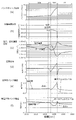
- FIG. 2 is a schematic diagram showing the configuration of the electron barrier layer 18A of the semiconductor light emitting device according to Comparative Example 1.
- Schematic diagrams (a), (b), (c), (d), and (e) show the band gap energy distribution of the semiconductor light emitting device according to Comparative Example 1, the polarization charge surface density distribution of the electron barrier layer 18A, and the polarization, respectively. The charge distribution, electric field distribution and band structure are shown.
- the semiconductor light emitting device according to Comparative Example 1 differs from the semiconductor light emitting device 100 according to the present embodiment in the distribution of the Al composition ratio of the electron barrier layer 18A.
- the Al composition ratio of the electron barrier layer 18 ⁇ / b> A according to Comparative Example 1 increases linearly from the active layer 15 side toward the second semiconductor layer 19 side.
- the third light guide layer 16 includes a composition ratio gradient region 16a. However, in this respect, it is not different from the semiconductor light emitting device 100 according to the present embodiment. .
- the polarization charge surface density formed in the nitride semiconductor depends on the sum of the piezopolarization component due to strain associated with the constituent layers and the natural polarization component as determined by the atomic composition. Therefore, the surface density of the polarization charge generated in each layer is constituted by the sum of the piezoelectric polarization component due to strain and the natural polarization component. Both the magnitude of strain generated in each layer and the magnitude of natural polarization are proportional to the atomic composition. For this reason, the surface density of the polarization charge formed in the AlGaN layer is proportional to the Al composition of the AlGaN layer. Therefore, the polarization charge surface density formed in the electron barrier layer 18A of Comparative Example 1 in which the Al composition ratio increases linearly increases linearly as shown in the schematic diagram (b) of FIG.
- the amount of polarization charge formed is constant in the electron barrier layer 18A as shown in the schematic diagram (c) of FIG. It is.
- a positive polarization charge is formed in the region on the active layer 15 side of the electron barrier layer 18A, and a negative polarization charge is formed at the interface far from the active layer 15.
- a negative polarization charge is formed at the interface far from the active layer 15.
- a negative electric field is generated due to electrons generated at the interface of the electron barrier layer 18A on the active layer 15 side.
- a decrease in potential at the interface of the electron barrier layer 18A in contact with the active layer 15 can be suppressed.
- the Al composition ratio on the active layer 15 side of the electron barrier layer 18A is small, and the forbidden band width energy (that is, band gap energy) is small. For this reason, the potential barrier formed in the valence band with respect to the holes on the active layer 15 side can be suppressed, and the operating voltage can be reduced.
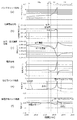
- FIG. 3 is a schematic diagram showing a configuration of the electron barrier layer 18 of the semiconductor light emitting device 100 according to the present embodiment.
- Schematic diagrams (a), (b), (c), (d), and (e) show the band gap energy distribution of the semiconductor light emitting device 100 according to the present embodiment and the polarization charge surface density distribution of the electron barrier layer 18, respectively. Shows polarization charge distribution, electric field distribution and band structure.
- the electron barrier layer 18 includes a first region having a small Al composition ratio change rate and a second region having a large Al composition ratio change rate in order from the active layer 15 side. .
- the polarization charge surface density distribution formed in the electron barrier layer 18 includes a region that changes with a relatively small inclination, and a region that changes with a relatively large inclination.
- the magnitude of the polarization charge is proportional to the rate of change in the polarization charge surface density, as shown in the schematic diagram (c) of FIG.
- the size of the distribution shown in (c) is small on the active layer 15 side.
- the magnitude of the polarization charge changes in two steps depending on the position in the stacking direction.
- a positive polarization charge is formed at the interface of the electron barrier layer 18 on the active layer 15 side, and a negative polarization charge is formed at the interface far from the active layer 15.
- carriers of opposite polarity are attracted to both interfaces in order to satisfy the electrical neutral condition.
- the electron concentration is smaller than that shown in the schematic diagram (c) of FIG.
- the semiconductor light emitting device 100 having a lower operating voltage and a smaller leakage current can be realized as compared with the conventional electron barrier layer.
- an ultra-high-power blue semiconductor laser element capable of long-term operation of several thousand hours or more can be realized even when high-wattage operation at the watt level is performed at a high temperature of 85 ° C.
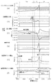
- FIGS. 4A and 4B are schematic views showing a first example and a second example of band gap energy distribution in the stacking direction of the electron barrier layer 18 of the semiconductor light emitting device 100 according to the present embodiment, respectively.
- FIG. 4A shows a band gap energy distribution when a first region having a small Al composition ratio change rate is in contact with a second region having an Al composition ratio change rate larger than the first region.
- FIG. 4B a region having a smaller composition ratio change rate than the first region is disposed between the first region having a smaller Al composition ratio change rate and the second region having the Al composition ratio change rate larger than the first region.
- the band gap energy distribution is shown.
- the Al composition ratio change rate of the first region where the electron barrier layer 18 starts to be formed is higher than the Al composition ratio change rate of the region to be formed thereafter. This increases the controllability of the position of the interface of the electron barrier layer 18 on the active layer 15 side, that is, the position where the electron barrier layer 18 begins to be formed, and has the effect of improving the stability of the reproducibility of the operating characteristics of the semiconductor light emitting device 100 is there.
- the electron barrier layer 18 includes the first region in which the Al composition ratio changes at the first change rate in the stacking direction perpendicular to the main surface of the GaN substrate 11,
- the second region is disposed between the second semiconductor layer 19 and the Al composition ratio changes at the second rate of change in the stacking direction.
- the Al composition ratio monotonously increases in the direction from the active layer 15 toward the second semiconductor layer, and the second rate of change is larger than the first rate of change.
- the influence of the magnitude of the polarization charge on the active layer 15 side interface of the electron barrier layer 18 can be made smaller than that of the electron barrier layer having the Al composition ratio distribution indicated by the dotted line in FIGS. 4A and 4B. it can.
- the decrease in the potential of the band structure at the interface of the electron barrier layer 18 on the active layer 15 side becomes smaller than that indicated by the dotted line, and the potential barrier ⁇ Ec increases.
- the band barrier against holes in the valence band can be reduced, the operating voltage of the semiconductor light emitting device 100 can be reduced. Accordingly, the temperature characteristics of the semiconductor light emitting device 100 can be improved. Therefore, the semiconductor light emitting device 100 with low power consumption can be realized even in high temperature operation.
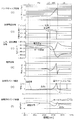
- 5A to 5D are schematic views showing third to sixth examples of band gap energy distribution in the stacking direction of the electron barrier layer 18 of the semiconductor light emitting device 100 according to the present embodiment, respectively.
- FIG. 5A shows a band gap energy distribution when a first region having a small Al composition ratio change rate is in contact with a second region having an Al composition ratio change rate larger than the first region. Furthermore, the Al composition ratio decreases from the Al composition ratio maximum point as it approaches the second semiconductor layer 19, and the first decreasing region having a large Al composition ratio decrease rate and the Al composition ratio decrease rate increase in order from the active layer 15 side. A second reduction region smaller than the first reduction region is disposed.
- FIG. 5B shows that a region having a smaller composition ratio change rate than the first region is formed between a first region having a small Al composition ratio change rate and a second region having a relatively large Al composition ratio change rate.
- the band gap energy distribution is shown.
- the Al composition ratio decreases from the Al composition ratio maximum point as it approaches the second semiconductor layer 19, and the first decreasing region having a large Al composition ratio decrease rate and the Al composition ratio decrease rate increase in order from the active layer 15 side.
- a second reduction region smaller than the first reduction region is disposed.
- FIG. 5C shows the bandgap energy distribution when the first region having a small Al composition ratio change rate and the second region having an Al composition ratio change rate larger than the first region are in contact with each other. Furthermore, in order from the active layer 15 side, a constant region where the Al composition ratio is constant from the Al composition ratio maximum point, a first decreasing region where the Al composition ratio decrease rate is large, and an Al composition ratio decreasing rate are greater than the first decreasing region. And a smaller second reduction region.
- a region having a composition ratio change rate smaller than the first region is formed between the first region having a small Al composition ratio change rate and the second region having the Al composition ratio change rate larger than the first region.
- the band gap energy distribution in the case is shown. Furthermore, in order from the active layer 15 side, a constant region where the Al composition ratio is constant from the Al composition ratio maximum point, a first decreasing region where the Al composition ratio decrease rate is large, and an Al composition ratio decreasing rate are higher than those of the first decreasing region. And a smaller second reduction region.
- the influence of the magnitude of the polarization charge on the active layer 15 side interface of the electron barrier layer 18 is made smaller than that of the electron barrier layer having the Al composition ratio distribution indicated by the dotted line. Can do.
- the decrease in the potential of the band structure at the interface of the electron barrier layer 18 on the active layer 15 side becomes smaller than that indicated by the dotted line, and the potential barrier ⁇ Ec increases.
- the band barrier against holes in the valence band can be reduced, the operating voltage of the semiconductor light emitting device 100 can be reduced. Accordingly, the temperature characteristics of the semiconductor light emitting device 100 can be improved.
- the second semiconductor layer 19 is formed of a superlattice composed of two types of AlGaN layers containing GaN and having different Al composition ratios
- the position where the Al composition ratio of the electron barrier layer 18 is the same.
- AlGaN having a high Al composition ratio the activation rate of Mg, which is usually used as a dopant, is low. For this reason, AlGaN with a high Al composition ratio has a higher resistance than AlGaN with a low Al composition ratio. Therefore, when the region having a high Al composition ratio in the electron barrier layer 18 is thickened, the film thickness of the region that forms a potential barrier that inhibits electrical conduction to the active layer 15 side of the holes in the band structure of the valence band. Since it is thick, hole conduction is hindered. Along with this, the operating voltage increases.
- the total film thickness of the second reduced region and the first reduced region which is a region that decreases with respect to the growth film thickness direction of the Al composition ratio, is preferably as thin as possible.
- the total film thickness is, for example, 4 nm or less.
- the total film thickness may be 2 nm or less.
- the average Al composition ratio in the region where the Al composition ratio decreases is smaller than the structure showing the constant Al composition ratio reduction rate indicated by the one-dot chain line in the figure, and the semiconductor An increase in operating voltage of the light emitting element 100 can be suppressed.
- a region where the Al composition ratio is constant is formed. This is a region formed in consideration of variations in the Al composition ratio within the same wafer surface when the semiconductor light emitting device 100 is manufactured. As a result, a constant maximum Al composition ratio can be obtained in the electron barrier layer 18 in the same wafer surface, so that the uniformity of the potential barrier ⁇ Ec in the wafer surface can be improved.
- the film thickness in the constant composition ratio region is preferably as thin as possible.
- the film thickness in the constant composition ratio region is, for example, 2 nm or less. Further, the film thickness in the constant composition ratio region may be 1 nm or less.
- FIG. 6 is a diagram illustrating an example of an Al composition ratio distribution in the stacking direction of the electron barrier layer 18 according to the present embodiment.
- a graph (a) in FIG. 6 is a graph showing a function f (x) indicating an Al composition ratio distribution.
- Graphs (b) and (c) in FIG. 6 are graphs showing the first derivative f ′ (x) and the second derivative f ′′ (x) of the function f (x), respectively.
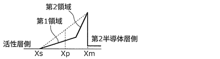
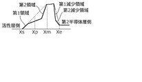
- the electron barrier layer 18 has a first concave region where f ′′ (x)> 0 and f ′ (x)> 0 in a region satisfying Xs ⁇ x ⁇ Xm. .
- f (x) has a concave shape (that is, a downward convex shape) as shown in the graph (a) of FIG. .
- the rate of change of the Al composition ratio is smaller on the active layer 15 side, and the magnitude of the polarization charge in the region near the interface on the active layer 15 side can be reduced.
- the magnitude of f ′ (x) is continuous, and there is no discontinuous position. For this reason, there is no position where the polarization charge surface density formed in the electron barrier layer 18 changes sharply. Therefore, it is possible to prevent a position where the positive polarization charge formed in the electron barrier layer 18 increases rapidly.
- the electron concentration in the region in the vicinity of the interface of the electron barrier layer 18 on the active layer 15 side can be reduced, and the operating voltage can be reduced.
- the electron barrier layer 18 has a first convex region that satisfies f ′′ (x) ⁇ 0 in a region that satisfies X1 ⁇ x ⁇ Xe with respect to the position x. .
- the function f (x) has a convex shape upward. Accordingly, the shape of the function f (x) is such that the first convex region that is convex upward is formed on the second semiconductor layer 19 side of the first concave region that is convex downward.
- the position x Xm at which the Al composition ratio is maximum is arranged in the first convex region.
- the Al composition ratio is higher than the average Al composition ratio of the second conductivity type second semiconductor layer, so This leads to an increase in the film thickness of the hindering region, resulting in an increase in operating voltage.
- the total film thickness of the second reduced region and the first reduced region should be as thin as possible.
- the total film thickness is, for example, 4 nm or less.
- the total film thickness may be 2 nm or less.
- the magnitude of the polarization charge in the vicinity of the interface of the electron barrier layer 18 on the active layer 15 side can be made smaller than that of the electron barrier layer having an Al composition ratio distribution indicated by g (x).
- the potential barrier ⁇ Ec increases.
- the band barrier against holes in the valence band can be reduced, the operating voltage of the semiconductor light emitting device 100 can be reduced. Accordingly, the temperature characteristics of the semiconductor light emitting device 100 can be improved.
- FIG. 7 is a diagram illustrating another example of the Al composition ratio distribution in the stacking direction of the electron barrier layer 18 according to the present embodiment.
- a graph (a) in FIG. 7 is a graph showing a function f (x) indicating an Al composition ratio distribution.
- Graphs (b) and (c) in FIG. 7 are graphs showing the first derivative f ′ (x) and the second derivative f ′′ (x) of the function f (x), respectively.
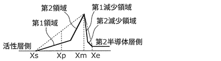
- f ′ (x) continuously changes in the region satisfying Xs ⁇ x ⁇ X1 with respect to the position x, f ′ (x)> 0, and the second derivative f ′′ (x).
- f ′ (x) continuously changes in the region satisfying Xs ⁇ x ⁇ X1 with respect to the position x, f ′ (x)> 0, and the second derivative f ′′ (x).
- the electron barrier layer 18 is a second region where f ′′ (x) ⁇ 0 in a region where Xs ⁇ x ⁇ X1 is satisfied at the position x. Has a convex region. Thereby, the Al composition ratio distribution shape of the second convex region becomes an upward convex shape.
- the increase rate of the Al composition ratio can be increased at the initial stage of formation of the electron barrier layer 18.
- a concave first concave region is formed on the second semiconductor layer 19 side of the second convex region. That is, the second convex region is disposed between the second concave region and the first concave region. In this case, a region with a large change rate in which the Al composition ratio increases is formed, and a region where a large polarization charge is generated can be kept away from the active layer 15 side.
- a convex first convex region is formed on the second semiconductor layer 19 side of the first concave region.
- the function f (x) is in contact with the point (Xu, f (Xu)) of the second convex area, and the function f (x) and the first convex area are A linear function contacting at the point (Xv, f (Xv)) is defined as a function h (x).
- the function f (x), the function h (x), and the first derivative f ′ (x) are h (x)> f (x) and f ′ (x )> 0 is satisfied.
- the polarization charge formed in the electron barrier layer is proportional to f ′ (x) as described above.
- the region where the positive polarization charge surface is formed relatively large is a region near the maximum value of f ′ (x) as shown in the graph (b) of FIG.
- the positive polarization charge near the position x Xv increases.
- the potential barrier ⁇ Ec can be increased.
- the band barrier potential for holes in the valence band can be reduced, the operating voltage of the semiconductor light emitting device 100 can be reduced. Accordingly, the temperature characteristics of the semiconductor light emitting device 100 can be improved.
- a region in which the Al composition ratio is higher than the average Al composition ratio of the second semiconductor layer 19 increases, so that the film in the region that inhibits hole conduction This leads to an increase in thickness and an increase in operating voltage.
- the total film thickness of the first reduction region and the second reduction region is preferably as thin as possible.
- the total film thickness is, for example, 4 nm or less.
- the total film thickness may be 2 nm or less.
- f (x) is an increasing function of a concave shape (that is, a downward convex shape).
- the electron concentration can be reduced.
- the decrease in the potential of the band structure at the interface of the electron barrier layer 18 on the active layer 15 side becomes smaller than the configuration indicated by g (x) or h (x), and the potential barrier ⁇ Ec increases. Furthermore, since the band barrier potential for holes in the valence band can be reduced, the operating voltage of the semiconductor light emitting device 100 can be reduced. Accordingly, the temperature characteristics of the semiconductor light emitting device 100 can be improved.
- the width of the first concave region is (Xm ⁇ Xs) / 2 or more.
- a region where the magnitude of the polarization charge becomes large can be arranged near the Al composition ratio maximum point Xm, so that the polarization charge generation position is the activity of the electron barrier layer 18. It can be kept away from the layer 15 side interface.
- the decrease in the potential of the band structure at the interface of the electron barrier layer 18 on the active layer 15 side becomes smaller than the configuration indicated by g (x) or h (x), and the potential barrier ⁇ Ec increases. . Furthermore, since the band barrier potential for holes in the valence band can be further reduced, the operating voltage of the semiconductor light emitting device 100 can be reduced. Accordingly, the temperature characteristics of the semiconductor light emitting device 100 can be improved.
- the electron barrier layer 18 of the semiconductor light emitting device 100 is doped with Mg.
- AlGaN having a high Al composition ratio is used in the first convex region of the electron barrier layer 18.
- the maximum Al composition ratio may be, for example, 0.2 or more, or 0.3 or more.
- the Mg doping concentration in the electron barrier layer 18 may be increased to 1 ⁇ 10 19 cm ⁇ 3 or more to increase the concentration of the acceptor to be activated.
- the Mg doping concentration may be less than 3 ⁇ 10 19 cm ⁇ 3 .
- the electron barrier layer 18 is doped with Mg of 1 ⁇ 10 19 cm ⁇ 3 or more and 2 ⁇ 10 19 cm ⁇ 3 or less.
- the Mg activation rate is high, so the concentration of Mg to be doped is 1 ⁇ . and 10 19 cm -3, may be increased relatively the concentration of Mg doping of 2 ⁇ 10 19 cm -3 in the first convex area near the Al composition ratio increases. Thereby, the crystallinity fall in the electron barrier layer 18 by the increase in Mg density
- the thickness of the first region is greater than 50% of the thickness of the electron barrier layer 18 and not more than 80%, and the position x
- the change rate of the Al composition ratio is small, and the second region on the second semiconductor layer 19 side is small. In the region, the change rate of the Al composition ratio is large.
- the Al composition ratio continuously changes in the region where the Al composition ratio of the electron barrier layer 18 changes.
- Such an Al composition ratio distribution of the electron barrier layer 18 can be formed by using, for example, MOCVD (Metal Organic Chemical Vapor Deposition).
- MOCVD Metal Organic Chemical Vapor Deposition
- the composition ratio distribution can be freely adjusted by temporally changing the supply amount of the gas containing the crystal raw material.
- Each shape of the Al composition ratio distribution described above can be realized by changing the Al supply amount in minute steps with respect to time.
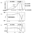
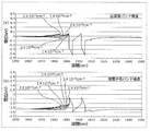
- FIG. 8 is a diagram showing a simulation result of the first configuration example of the semiconductor light emitting element 100 according to the present embodiment.
- FIG. 9 is a diagram illustrating simulation results of the semiconductor light emitting element according to Comparative Example 2.
- FIG. 10 is a diagram illustrating a simulation result of the second configuration example of the semiconductor light emitting element 100 according to the present embodiment.
- FIG. 11 is a diagram illustrating a simulation result of the third configuration example of the semiconductor light emitting element 100 according to the present embodiment.
- FIG. 12 is a diagram illustrating a simulation result of the semiconductor light emitting element according to Comparative Example 3. In each simulation, the operating current of the semiconductor light emitting element is 300 mA.
- Each graph (a) in FIGS. 8 to 12 shows the distribution of the forbidden band width energy (band gap) near the electron barrier layer, and each graph (b) shows the polarization charge per unit volume near the electron barrier layer. Show the distribution.
- Each graph (c) in FIGS. 8 to 12 shows the distribution of electron and hole concentrations in the vicinity of the electron barrier layer, and each graph (d) shows the electric field distribution in the vicinity of the electron barrier layer 18.
- Each graph (e) in FIGS. 8 to 12 shows a conduction band structure near the electron barrier layer 18 and a distribution of electron Fermi energy, and each graph (f) shows a valence band near the electron barrier layer 18. The band structure and the Fermi energy distribution of holes (ie holes) are shown.
- FIG. 8 shows a simulation result when the thickness of the electron barrier layer 18 is 7 nm.
- the electron barrier layer 18 has a first region having a thickness of 5 nm and a second region having a thickness of 2 nm.
- the Al composition ratio is linearly increased from 0 to 0.15 as it proceeds from the active layer 15 side to the second semiconductor layer 19 side.
- the Al composition ratio is increased from 0.15 to 0.35 as it proceeds from the active layer 15 side to the second semiconductor layer 19 side.
- a positive polarization charge of 1 ⁇ 10 19 cm ⁇ 3 is generated on the active barrier 15 side of the electron barrier layer 18 and 5 ⁇ 10 19 on the second semiconductor layer side.
- a positive polarization charge of cm ⁇ 3 is generated.
- This polarization charge corresponds to, for example, about 1% compared to the case where the electron barrier layer has a uniform Al composition ratio of 0.35.
- negative polarization charges having a surface density of ⁇ 5.3 ⁇ 10 ⁇ 2 C / m 2 are formed at the interface between the electron barrier layer 18 and the second semiconductor layer 19. .
- the film thickness of the interface is 0.01 nm, which is about several tenths of the c-axis direction lattice constant of AlGaN. Then, it is considered that a negative polarization charge corresponding to about 1 ⁇ 10 22 cm ⁇ 3 in terms of electron concentration is generated at the interface.
- the electron barrier layer 18 according to the present embodiment polarization charges on the active layer 15 side can be suppressed.
- the volume density of the polarization charge is a value converted to an electron concentration.
- the decrease in the barrier ⁇ Ec and the increase in the potential barrier ⁇ Ev against holes are suppressed.
- the potential barrier ⁇ Ec is 0.77 eV
- the potential barrier ⁇ Ev is 0.22 eV.
- the Al composition ratio distribution of the electron barrier layer 18 is concave (convex downward) like the electron barrier layer 18 shown in FIG. It was found that the potential barrier ⁇ Ec for electrons was larger and the potential barrier ⁇ Ev for holes was smaller.
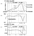
- FIG. 9 shows a simulation result of a semiconductor light emitting device that is different from the present embodiment only in the configuration of the electron barrier layer 18B as Comparative Example 2 of the semiconductor light emitting device 100 according to the present embodiment.
- the thickness of the electron barrier layer 18B according to Comparative Example 2 is set to 7 nm, and the Al composition ratio is increased from 0 to 0.35 as the electron barrier layer 18B progresses from the active layer 15 side to the second semiconductor layer 19 side. Yes.
- the Al composition ratio is increased so that the increase rate of the Al composition ratio gradually decreases. That is, the graph of the Al composition ratio distribution is not a straight line but a convex shape upward.
- a positive polarization charge of 5 ⁇ 10 19 cm ⁇ 3 is generated on the active layer 15 side of the electron barrier layer 18B.
- only positive polarization charges are displayed. This value is five times the value generated in the simulation of the semiconductor light emitting device 100 according to the present embodiment shown in FIG.
- negative polarization charges having a surface density of ⁇ 5.3 ⁇ 10 ⁇ 2 C / m 2 are formed at the interface between the electron barrier layer 18 and the second semiconductor layer 19. .
- the film thickness of the interface is 0.01 nm, which is about several tenths of the c-axis direction lattice constant of AlGaN. Then, it is considered that a negative polarization charge corresponding to about 1 ⁇ 10 22 cm ⁇ 3 in terms of electron concentration is generated at the interface.
- the decrease in the potential of the conduction band and the valence band in the interface of the electron barrier layer 18B on the active layer 15 side is also compared with the result shown in FIG. And get bigger.
- the potential barrier ⁇ Ec for electrons decreases and the potential barrier ⁇ Ev for holes increases.
- the potential barrier ⁇ Ec for electrons is 0.68 eV
- the potential barrier ⁇ Ev for holes is 0.28 eV.
- FIG. 10 shows a simulation result when the thickness of the electron barrier layer 18 is 7 nm.
- the Al composition ratio is gradually increased from 0 to 0.15 (straight line) as it proceeds from the active layer 15 side to the second semiconductor layer 19 side in the 5 nm thick region of the electron barrier layer 18 on the active layer 15 side. Increase).
- the Al composition is increased so that the increasing rate of the Al composition ratio increases as it proceeds from the active layer 15 side to the second semiconductor layer 19 side.
- the ratio is increased to 0.35.
- the Al composition ratio distribution has a concave shape (convex shape downward) in the region of the film thickness of 2 nm on the second semiconductor layer 19 side of the electron barrier layer 18.
- the area near the active layer 15 of the electron barrier layer 18 decreases from 2 ⁇ 10 19 cm ⁇ 3 to 1 ⁇ 10 19 cm ⁇ 3 as the distance from the active layer 15 increases. As a result, positively distributed charges are generated.
- the graph (b) of FIG. 10 only positive polarization charges are displayed.
- negative polarization charges having a surface density of ⁇ 5.3 ⁇ 10 ⁇ 2 C / m 2 are formed at the interface between the electron barrier layer 18 and the second semiconductor layer 19. .
- the film thickness of the interface is 0.01 nm, which is about several tenths of the c-axis direction lattice constant of AlGaN. Then, it is considered that a negative polarization charge corresponding to about 1 ⁇ 10 22 cm ⁇ 3 in terms of electron concentration is generated at the interface.
- the graph (c) of FIG. 10 shows 1 ⁇ 10 17 at the interface of the electron barrier layer 18 on the active layer 15 side in order to satisfy the electrical neutral condition with the positive polarization charge generated at the interface of the electron barrier layer 18.
- An electron with a concentration of cm ⁇ 3 is attracted. This concentration is suppressed to about one-tenth of the case shown in the graph (c) of FIG. For this reason, the electric field generated at the interface of the electron barrier layer 18 on the active layer 15 side is ⁇ 0.3 MV / cm and its absolute value is suppressed.
- the potential drop of the conduction band and the valence band at the interface of the electron barrier layer 18 on the active layer 15 side is also suppressed.
- ⁇ Ec increases and the potential barrier ⁇ Ev against holes decreases.
- the potential barrier ⁇ Ec for electrons is 0.77 eV
- the potential barrier ⁇ Ev for holes is 0.23 eV.
- Al composition ratio decreasing region a region in which the Al composition ratio decreases from the active layer 15 side to the second semiconductor layer 19 side toward the second semiconductor layer 19 side of the electron barrier layer shown in FIG.
- the electron barrier layer 18 having a configuration with 2 nm added) also referred to as “Al composition ratio decreasing region” is used.
- the Al composition ratio decreasing region is an Al composition in which a region having a concave shape (that is, a convex shape downward) is formed on the second semiconductor layer 19 side of a region where the Al composition ratio distribution shape is convex upward. Has a ratio distribution.
- the distance from the active layer 15 toward the active layer 15 side of the electron barrier layer 18 decreases from 2 ⁇ 10 19 cm ⁇ 3 to 1 ⁇ 10 19 cm ⁇ 3 .
- a positive polarization charge distributed in the region is generated.
- only the positive polarization charge is displayed.
- negative polarization charges of about 2 ⁇ 10 20 cm ⁇ 3 are generated, although not shown.
- the graph (c) of FIG. 11 shows 1 ⁇ 10 17 at the interface of the electron barrier layer 18 on the active layer 15 side in order to satisfy the electrical neutral condition with the positive polarization charge generated at the interface of the electron barrier layer 18.
- An electron with a concentration of cm ⁇ 3 is attracted.
- This electron concentration is the same value as the configuration shown in FIG. 10, but since an Al composition ratio decreasing region is added to the second semiconductor layer 19 side of the electron barrier layer 18, it is shown in the graph (f) of FIG. As described above, the minimum value of the potential of the valence band structure decreases and the potential barrier ⁇ Ev against holes increases, so that the operating voltage of the semiconductor light emitting device 100 increases.
- the decrease in the potential of the conduction band and the valence band at the interface of the electron barrier layer 18 on the active layer 15 side is also reduced compared to the structure shown in FIG. Has been. For this reason, the potential barrier ⁇ Ec for electrons is lowered, and the potential barrier ⁇ Ev for holes is increased. In the structure shown in FIG. 11, the potential barrier ⁇ Ec for electrons is 0.68 eV, and the potential barrier ⁇ Ev for holes is 0.28 eV.
- the potential barrier ⁇ Ev against holes is increased by about 0.05 eV as compared with the configuration shown in FIG. 10, and the rising voltage of the semiconductor light emitting device 100 is increased by about 0.04 V in the current-voltage characteristics.
- the Al composition ratio decreasing region of the electron barrier layer 18 is preferably as thin as possible.
- FIG. 12 shows a simulation result of a semiconductor light emitting device that is different from the present embodiment only in the configuration of the electron barrier layer 18C as Comparative Example 3 of the semiconductor light emitting device 100 according to the present embodiment.
- the electron barrier layer 18C according to Comparative Example 3 has a thickness of 9 nm, and the electron barrier layer 18C has a thickness of 7 nm on the active layer 15 side, from the active layer 15 side of the electron barrier layer 18C to the second semiconductor layer 19 side.
- the Al composition ratio is increased from 0 to 0.35.
- the Al composition ratio decreasing region having a film thickness of 2 nm on the second semiconductor layer 19 side of the electron barrier layer 18C the Al composition ratio is made the same as that of the second semiconductor layer 19 from the active layer 15 side to the second semiconductor layer 19 side. It decreases until it becomes.
- the Al composition ratio decreasing region is an Al composition in which a region having a concave shape (that is, a convex shape downward) is formed on the second semiconductor layer 19 side of a region where the Al composition ratio distribution shape is convex upward. Has a ratio distribution.
- the graph (c) of FIG. 12 shows 2 ⁇ 10 17 at the interface of the electron barrier layer 18 C on the active layer 15 side in order to satisfy the electrical neutral condition with the positive polarization charge generated at the interface of the electron barrier layer 18.
- An electron with a concentration of cm ⁇ 3 is attracted.
- the electron concentration is increased to about twice that of the configuration shown in FIG. This is because the Al composition ratio in the 7 nm-thickness region of the electron barrier layer 18C on the active layer 15 side is larger than the configuration shown in FIG. That is, the attracted electron concentration can be reduced when the Al composition ratio distribution has a concave shape as in the configuration shown in FIG.
- FIG. 13 is a schematic diagram showing the Al composition ratio distribution shape of the electron barrier layer used in the simulation.
- 14 and 15 are graphs showing simulation results when the thickness of the electron barrier layer is 5 nm and 15 nm, respectively.
- the maximum Al composition ratio of the electron barrier layer, the maximum Al composition ratio of the first region, and the thickness of the first region are changed in each case where the thickness of the electron barrier layer is 5 nm and 15 nm.
- the operating voltage at an operating current value of 300 mA and the potential barrier ⁇ Ec against electrons were estimated, and a shape effective for suppressing electron leakage and reducing the voltage was examined.
- Graphs (a) to (e) of FIG. 14 show the calculation results of the film thickness dependence of the first region of the operating voltage during 300 mA operation, and graphs (f) to (j) show the potential barrier ⁇ Ec of the electrons.
- region is shown.
- Graphs (a) and (f) show the calculation results when the maximum Al composition ratio is 0.15 and the maximum Al composition ratio of the first region is 0.05, 0.1, and 0.15.
- the maximum Al composition ratio is 0.2
- the maximum Al composition ratio in the first region is 0.05, 0.1, 0.15, and 0.2. The calculation result is shown.
- the maximum Al composition ratio is 0.25, and the maximum Al composition ratio of the first region is 0.05, 0.1, 0.15, 0.2, 0.25. The calculation results in each case are shown.
- the maximum Al composition ratio is 0.3, and the maximum Al composition ratio of the first region is 0.05, 0.1, 0.15, 0.2, 0.25. The calculation result in each case of 0.3 is shown.
- the maximum Al composition ratio is 0.35, and the maximum Al composition ratio of the first region is 0.05, 0.1, 0.15, 0.2, 0.25. , 0.3, and 0.35 are shown in FIG.
- the points indicated by white circles are a region where the Al composition ratio distribution shape shown in FIG. 13 is a concave shape (that is, a convex shape downward), and a convex shape (that is, a convex shape that is upward).
- Graphs (a) to (j) in FIG. 15 are graphs showing calculation results similar to the graphs (a) to (j) in FIG. 14 except that the thickness of the electron barrier layer is 15 nm. .
- the point indicated by a white circle represents the film thickness of the first region having a “linear shape” as in each graph of FIG.
- the maximum Al composition ratio in the electron barrier layer is 0.15 or more and 0.35 or less, and the maximum Al composition ratio in the first region is 0.05 or more.
- the maximum Al composition ratio of the first region is not more than a composition ratio that is 50% of the maximum Al composition ratio in the electron barrier layer, and the film thickness of the first region is the electron barrier. If it is 50% or more of the film thickness of the layer, the value is equal to or lower than the operating voltage in the case of a linear shape.
- the maximum Al composition ratio of the electron barrier layer is the maximum Al composition ratio of the first region. Therefore, as the film thickness of the first region approaches the film thickness of the electron barrier layer, the film thickness of the region where the forbidden band energy of the electron barrier layer is large becomes thin. For this reason, due to the influence of the quantum mechanical tunnel effect, the potential barrier ⁇ Ec against electrons approaches the value of ⁇ Ec when the maximum Al composition ratio of the electron barrier layer is the maximum Al composition ratio of the first region.
- the maximum Al composition ratio in the electron barrier layer is 0.15 or more and 0.35 or less, and the maximum Al composition ratio in the first region is 0.05 or more. In the range of 0.35 or less, if the film thickness of the first region is 80% or less of the film thickness of the electron barrier layer, a decrease in the potential barrier ⁇ Ec for electrons can be suppressed.
- the maximum Al composition ratio of the first region is equal to or less than the composition ratio that is 50% of the maximum Al composition ratio of the electron barrier layer, and the film thickness of the first region is If the thickness of the electron barrier layer is not less than 50% and not more than 80%, the operating voltage can be suppressed as compared with the case of a linear shape, and the decrease in ⁇ Ec accompanying the thinning of the high Al composition ratio region of the electron barrier layer can be reduced. Can be suppressed.
- the thickness of the electron barrier layer is 2 nm or less, generation of tunnel current and electrons existing at the interface of the electron barrier layer on the active layer side are thermally excited due to the thinning of the thickness of the electron barrier layer. Overflow of electrons exceeding the electron barrier layer is likely to occur.
- the maximum value of the Al composition ratio of the electron barrier layer is increased to 15% or more, it is necessary to dope Mg at a high concentration. If the thickness of the electron barrier layer is increased, the waveguide loss is increased. .
- the thickness of the electron barrier layer must be 3 nm or more and 20 nm or less.
- the thickness of the electron barrier layer is in the range of 5 nm or more and 15 nm or less, and the maximum Al composition ratio of the first region is not more than a composition ratio that is 50% of the maximum Al composition ratio in the electron barrier layer.
- the film thickness of the first region may be 50% or more and 80% or less of the film thickness of the electron barrier layer.
- the thickness of the electron barrier layer is 7 nm
- the thickness of the first region is 4 nm
- the thickness of the second region is 3 nm, so that both improvement in temperature characteristics and reduction in operating voltage are achieved.
- FIG. 16 is a schematic diagram showing an impurity doping profile of the second semiconductor layer 19 in the semiconductor light emitting device 100 according to the present embodiment.
- the second semiconductor layer 19 includes, in order from the electron barrier layer 18 side, a low impurity concentration region 19a having an impurity concentration P2 and a film thickness X2, and a high impurity concentration region 19b having an impurity concentration P3.
- the waveguide loss is reduced by reducing the free carrier loss that the light distribution suffers in the second semiconductor layer 19.
- the film thickness X2 and the impurity concentration P2 of the low impurity concentration region 19a for realizing the low waveguide loss while suppressing the increase of the operating voltage are examined.
- N1 shown in FIG. 16 is the concentration of the n-type impurity made of Si in the first semiconductor layer 12 made of n-type AlGaN and the first light guide layer 13 made of n-type GaN.
- N1 is 1 ⁇ 10 18 cm ⁇ .
- P4 shown in FIG. 16 is the concentration of the p-type impurity made of Mg in the contact layer 20 made of p-type GaN, and here, it is 1 ⁇ 10 20 cm ⁇ 3 .
- FIG. 17A and 17B are graphs showing the dependence of the operating voltage and waveguide loss on the impurity concentration of the low impurity concentration region 19a in the semiconductor light emitting device 100 according to the present embodiment, respectively.
- FIG. 17A and FIG. 17B show the operating voltage at 300 mA operation when the impurity concentration P2 is in the range of 0.5 ⁇ 10 18 cm ⁇ 3 to 1 ⁇ 10 19 cm ⁇ 3 , and the impurity of the waveguide loss, respectively. Concentration is indicated.
- 17A and 17B show the calculation results of the dependency when the film thickness X2 of the low impurity concentration region 19a is 50 nm, 170 nm, 270 nm, and 370 nm.
- the waveguide loss reduction effect is large when the film thickness of the low impurity concentration region 19a is 170 nm or more.
- a low operating voltage and a low waveguide loss are realized by setting the film thickness of the low impurity concentration region 19a to 170 nm and the Mg doping concentration to 2 ⁇ 10 18 cm ⁇ 3 .
- the increase in operating voltage at 300 mA operation is suppressed to 0.1 V compared to the case where the impurity doping of the second semiconductor layer 19 is constant at 1 ⁇ 10 19 cm ⁇ 3 , and Waveguide loss can be halved from 7 cm ⁇ 1 to 4 cm ⁇ 1 .
- FIG. 18 shows the valence band structure and hole Fermi when the impurity doping concentration of the low impurity concentration region 19a according to the present embodiment is changed from 1 ⁇ 10 17 cm ⁇ 3 to 1 ⁇ 10 19 cm ⁇ 3. It is a graph which shows the calculation result of a level.
- the Mg doping concentration of the high impurity concentration region 19b of the second semiconductor layer 19 is set to 1 ⁇ 10 19 cm ⁇ 3 .
- the Mg doping concentration in the concentration region 19a may be controlled in the range of 1 ⁇ 10 18 cm ⁇ 3 or more and 2 ⁇ 10 18 cm ⁇ 3 or less.
- the film thickness of the low impurity concentration region 19a is changed from 150 nm to 200 nm, and the Mg doping concentration is 1 ⁇ 10 18 cm ⁇ 3 or more, 2 Control within a range of ⁇ 10 18 cm ⁇ 3 or less does not cause an increase in waveguide loss and operating voltage, and can suppress the generation of high energy holes due to the inclination of the band structure of the valence band. As a result, it is possible to improve the high-temperature operating characteristics and reduce the operating current value, so that the operation reliability of the semiconductor light emitting device 100 can be improved.
- FIG. 19 is a graph showing the characteristics of the semiconductor light emitting device when the Al composition ratio distribution shape of the electron barrier layer is set to the shape a, the shape b, and the shape c.
- the shape a corresponds to the Al composition ratio distribution shape of the electron barrier layer according to the present embodiment
- the Al composition ratio is linear from 0 to 0.15 in the first region having a film thickness of 4 nm on the active layer side.
- the Al composition ratio is linearly increased from 0.15 to 0.35.
- the Al composition ratio increases linearly from 0 to 0.35 to the maximum value as it proceeds from the active layer side to the second semiconductor layer side. In the region of film thickness of 3 nm on the layer side, the Al composition ratio is constant at a maximum value of 0.35.
- the shape c is a shape in which the Al composition ratio distribution in the 7 nm-thick electron barrier layer is constant at 0.35.
- a graph (a) in FIG. 19 shows current-light output characteristics at 25 ° C.
- a graph (b) shows current-voltage characteristics at 25 ° C.
- a graph (c) shows current-light output characteristics at 85 ° C.
- Graph (d) shows the measurement results of current-voltage characteristics at 85 ° C.
- the Al composition ratio in the first region of the electron barrier layer, a shape in which the Al composition ratio is increased from 0 to 0.15 in the 4 nm-thickness region in the Al composition ratio distribution shape is adopted, and in the second region, A shape in which the Al composition ratio is increased from 0.15 to 0.35 in a region with a film thickness of 3 nm is employed.
- the film thicknesses of the first region and the second region of the shape a are the above-described film thicknesses. It is not limited to.
- the measurement results shown in FIG. 19 were obtained using a semiconductor light emitting device mounted on a submount made of diamond with a junction down so that the active layer side was close to the submount side.
- this mounting form reduces the thermal resistance of the semiconductor light emitting device, the temperature characteristics are improved.
- the thermal conductivity of diamond is 1000 W / m ⁇ K or more, and materials used for other submounts, for example, thermal conductivity of 200 W.
- SiC about / m ⁇ K
- AlN with a thermal conductivity of about 150 W / m ⁇ K, etc., it is suitable for realizing heat resistance. Therefore, the temperature rise of the semiconductor light emitting element during high temperature and high output operation is also reduced.
- thermal resistance in addition to mounting on a diamond submount with junction down, mounting on a single crystal SiC submount with junction down, or with a resonator length of 1200 ⁇ m or more and a stripe width of 40 ⁇ m
- the case where heat dissipation is improved and thermal resistance is reduced can be considered.
- the stripe width may be 40 ⁇ m or more and the resonator length may be 1500 ⁇ m or more from the viewpoint of heat dissipation.
- the reduction of the operating voltage by the electron barrier layer according to the present embodiment becomes even more effective.
- the semiconductor light emitting device according to the present embodiment includes the semiconductor according to the first embodiment in the impurity doping configuration in the third light guide layer and the impurity doping configuration in the barrier layer on the second light guide layer side of the active layer or the interface thereof. Different from the light emitting element 100.
- the semiconductor light emitting device according to the present embodiment will be described focusing on differences from the semiconductor light emitting device 100 according to the first embodiment.
- the semiconductor light emitting element according to the present embodiment has a layer structure as shown in FIG. 1A as in the semiconductor light emitting element 100 according to the first embodiment.
- the semiconductor light emitting device according to the present embodiment is different from the semiconductor light emitting device 100 according to the first embodiment in the configuration of the third light guide layer 16 and the barrier layer 15a of the active layer 15.
- the configurations and effects of the third light guide layer 16 and the barrier layer 15a will be described.
- FIG. 20 is a schematic diagram for explaining the formation of polarization charges in the composition ratio gradient region 16a of the third light guide layer 16 of the semiconductor light emitting device according to the present embodiment.
- FIG. 20 schematically shows a band structure (that is, a forbidden band width energy) in a region near the composition ratio gradient region 16 a of the third light guide layer 16.
- the schematic diagram (b) of FIG. 20 schematically shows the polarization charge distribution in the region near the composition ratio gradient region 16 a of the third light guide layer 16.
- a schematic diagram (c) and a schematic diagram (d) of FIG. 20 schematically show an Mg doping profile in a region near the composition ratio gradient region 16 a of the third light guide layer 16.
- the profile shown in the schematic diagram (c) has a uniform Mg doping concentration in the composition ratio gradient region 16a.
- the Mg doping concentration is inclined in the composition ratio inclined region 16a.
- the schematic diagram (e) schematically shows the conduction band structure in the vicinity of the composition ratio gradient region 16 a of the third light guide layer 16.
- FIG. 21 is a schematic diagram for explaining the formation of polarization charges in the third light guide layer 16 of the semiconductor light emitting device according to Comparative Example 4.
- the semiconductor light emitting device according to Comparative Example 4 shown in FIG. 21 is different from the semiconductor light emitting device according to the present embodiment in that the third light guide layer 16 does not have a composition ratio gradient region, and is identical in other points. To do.
- the schematic diagram (a) of FIG. 21 schematically shows the band structure (that is, the forbidden bandwidth energy) in the vicinity of the third light guide layer 16.
- the schematic diagram (b) of FIG. 21 schematically shows the polarization charge distribution in the region near the third light guide layer 16.
- Mg doping profile in a region in the vicinity of the composition ratio gradient region 16 a arranged at the end of the third light guide layer 16 on the electron barrier layer 18 side.
- Mg is doped in a uniform distribution in the region on the electron barrier layer 18 side in the third light guide layer 16.
- the schematic diagram (d) schematically shows the conduction band structure in the vicinity of the third light guide layer 16.
- the composition ratio gradient region 16a in which the In composition ratio distribution is inclined at the boundary between the intermediate layer 17 and the third light guide layer 16 is formed. Note that the semiconductor light emitting device according to Comparative Example 4 does not have the composition ratio gradient region 16a.
- the third light guide layer 16 does not have the composition ratio gradient region 16a, a positive polarization charge is formed at the interface between the intermediate layer 17 and the third light guide layer 16 as shown in FIG. For this reason, the band structure is deformed so as to satisfy the electrical neutral condition, and electrons are attracted to the interface between the intermediate layer 17 and the third light guide layer 16. As a result, a dent as shown in the schematic diagram (d) of FIG. 21 is generated in the band structure of the interface, and this dent serves as a potential barrier against holes. For this reason, in the semiconductor light emitting device according to Comparative Example 4, the operating voltage increases.
- the third light guide layer 16 has the composition ratio gradient region 16a, as shown in the schematic diagram (b) of FIG. 20, the positive light formed at the interface between the intermediate layer 17 and the third light guide layer 16 is used.
- the polarization charges are dispersed at a small density throughout the composition ratio gradient region 16a. For this reason, the deformation of the band structure is small as shown in the schematic diagram (e) of FIG. 20, and the dent as shown in FIG. 21 does not occur. For this reason, an increase in the operating voltage of the semiconductor light emitting element can be suppressed.
- the hole concentration in the active layer 15 can be increased, and the operating voltage can be further reduced.
- the concentration on the active layer 15 side is low in the composition ratio gradient region 16a, the free carrier loss of the light distribution received by the third light guide layer 16 is reduced.
- production can be suppressed and the increase in waveguide loss can be suppressed, aiming at low voltage.
- FIGS. 22A to 22C show the semiconductor according to the present embodiment when the Mg doping concentration is 5 ⁇ 10 18 cm ⁇ 3 , 1 ⁇ 10 19 cm ⁇ 3 and 2 ⁇ 10 19 cm ⁇ 3 , respectively.
- the Mg doping region has the same film thickness as the composition ratio gradient region 16a, and the composition ratio gradient region thickness is changed.
- the solid line in each figure represents the case where Mg doping is performed at a uniform concentration in the composition ratio gradient region 16a, and the dotted line represents the case where gradient doping with a low Mg doping concentration on the active layer 15 side is performed.
- the operating voltage is reduced by about 0.01 V when the Mg doping concentration is increased.
- the longer the Mg doping region length the lower the operating voltage.
- the waveguide loss increases.
- the Mg doping concentration is 5 ⁇ 10 18 cm ⁇ 3
- the effect of reducing the operating voltage can be obtained if the Mg doping region length is about 10 nm.
- the Mg doping concentration is 1 ⁇ 10 19 cm ⁇ 3
- the effect of reducing the operating voltage can be obtained if the Mg doping region length is about 5 nm.
- the effect of reducing the operating voltage can be obtained if the Mg doping region length is about 3 nm.
- the effect of reducing the operating voltage is almost the same in both the case where uniform doping is performed in the composition ratio gradient region 16a and the case where gradient doping is performed. Therefore, from the viewpoint of suppressing an increase in waveguide loss, the composition ratio gradient region 16a may be doped with Mg.
- Mg doping to the composition ratio gradient region 16a not only the effect of lowering the operating voltage but also the effect of increasing the electrical conductivity of holes at a lower operating voltage can be achieved. For this reason, Mg doping to the composition ratio gradient region 16a is very important from the viewpoint of improving temperature characteristics during high-temperature, high-power operation at the watt level and ensuring long-term operation reliability.
- the composition ratio gradient region 16a In the composition ratio gradient region 16a, the case where the In composition ratio on the electron barrier layer 18 side is changed to the same In composition ratio as that of the intermediate layer 17 made of p-type GaN (that is, up to the In composition ratio of 0) will be considered. In this case, if Mg doping is performed on the interface of the composition ratio gradient region 16a as described above, the interface on the electron barrier layer 18 side of the composition ratio gradient region 16a is p-type GaN. There may be no intermediate layer of the second conductivity type.
- the semiconductor light emitting device has a region doped with an n-type impurity in the barrier layer 15a or at least one of the interfaces between the second light guide layer 14 and the barrier layer 15a.
- the influence of the negative polarization charge generated at the interface between the second light guide layer 14 and the barrier layer 15a is canceled, and the potential of the valence band of the barrier layer 15a is lowered, so that the well layer 15b and the well layer 15d
- the shape of the band structure of the valence band can be made uniform. Thereby, the uniformity of the shape of the quantum wave function formed by the two layers of the well layer 15b and the well layer 15d can be improved. For this reason, the wavelength at which the highest amplification gain can be obtained in each well layer can be made closer, so that the amplification gain can be increased. Thereby, the oscillation threshold current value required for laser oscillation can be reduced.
- the impurity doping according to the present embodiment it is possible to suppress the occurrence of hole overflow in which holes leak to the first light guide layer. For this reason, the temperature characteristics of the semiconductor light emitting device can be improved.
- FIG. 23 is a schematic diagram showing an aspect of impurity doping according to the present embodiment.
- the schematic diagram (a) of FIG. 23 shows the polarization charge per unit volume formed at the interface of each layer of the active layer 15.
- the schematic diagram (b) shows the band structure in the vicinity of the active layer 15.
- Schematic (c) shows an impurity doping profile when doping the barrier layer 15a
- (d) shows an impurity doping profile when doping the interface between the barrier layer 15a and the second light guide layer 14. Show.
- the semiconductor light emitting device has at least one of the barrier layer 15a or the interface between the second light guide layer 14 and the barrier layer 15a.
- the structure has a region doped with an n-type impurity.
- Si is doped as an impurity.
- FIG. 24 is a graph showing a conduction band structure and a valence band structure when the barrier layer 15a is doped with Si in the semiconductor light emitting device according to the present embodiment.
- the graph (a) in FIG. 24 shows the calculation result of the doping concentration dependency of the conduction band structure
- the graph (b) shows the calculation result of the doping concentration dependency of the valence band band structure.
- the band structure changes so as to satisfy the electrical neutral condition at this interface. Furthermore, holes are generated due to the negative polarization charge. Therefore, the potential at the interface increases. For this reason, in order to suppress an increase in the band potential of the valence band by compensating for the negative polarization charge generated at the interface between the second light guide layer 14 and the barrier layer 15a, an n-type is formed in the vicinity of this interface. It is effective to dope impurities.
- the Si doping concentration in the barrier layer 15a when the Si doping concentration in the barrier layer 15a is increased, the potential of the band structure of the valence band of the barrier layer 15a is lowered, and the valences of the well layer 15b and the well layer 15d are reduced.
- the shape of the band structure of the electronic band is made uniform.
- by increasing the potential barrier of the valence band on the second light guide layer 14 side of the barrier layer 15a it is possible to suppress the wave function of holes from spreading to the second light guide layer 14 side. This increases the cross-correlation of the electron and hole wave functions.
- the amplification gain for the injected carriers in the well layer 15b can be increased, so that the oscillation threshold current value can be reduced.
- the Si doping concentration in the barrier layer 15a increases, the effect of increasing the potential barrier in the valence band on the second light guide layer 14 side increases. From the result shown in the graph (b) of FIG. Is 5 ⁇ 10 18 cm ⁇ 3 or more, the potential barrier of the valence band is increased and the uniformity of the band structure of the valence band of the well layer 15b and the well layer 15d can be sufficiently enhanced.
- FIG. 25 is a graph showing a conduction band structure and a valence band structure when Si is doped at the interface between the barrier layer 15a and the second light guide layer 14 in the semiconductor light emitting device according to the present embodiment.
- the graph (a) in FIG. 25 shows the calculation result of the doping concentration dependency of the conduction band structure
- the graph (b) shows the calculation result of the doping concentration dependency of the valence band band structure.
- Si is doped in a region within ⁇ 5 nm from the interface between the barrier layer 15 a and the second light guide layer 14.
- the Si doping concentration at the interface between the barrier layer 15a and the second light guide layer 14 is increased, the potential of the band structure of the valence band of the barrier layer 15a is decreased.
- the shape of the band structure of the valence band of the well layer 15b and the well layer 15d is made uniform.
- the potential barrier of the valence band on the second light guide layer 14 side of the barrier layer 15a it is possible to suppress the wave function of holes from spreading to the second light guide layer 14 side.
- the cross-correlation between the wave functions of electrons and holes is increased, and the amplification gain for the injected carriers in the well layer 15b can be increased, so that the oscillation threshold current value can be reduced.
- the effect of suppressing the overflow of holes is the second when Si doping is performed on the interface between the barrier layer 15a and the second light guide layer 14.
- the potential of the valence band of the light guide layer 14 also decreases. For this reason, it is possible to enhance the effect of suppressing the spreading of the wave function of holes to the second light guide layer 14 and suppressing the overflow of holes.
- the effect of increasing the potential barrier of the valence band on the second light guide layer 14 side increases.
- the potential barrier of the valence band increases and the band structure of the valence band of the well layer 15b and the well layer 15d. Can be sufficiently improved in uniformity.
- FIG. 3 A semiconductor light emitting device according to the third embodiment will be described.
- the semiconductor light emitting device according to the present embodiment is different from the semiconductor light emitting device according to the second embodiment in the configuration of the barrier layer of the active layer 15.
- the semiconductor light emitting device according to the present embodiment will be described focusing on differences from the semiconductor light emitting device according to the second embodiment.
- the barrier layer 15a, the barrier layer 15c, and the barrier layer 15e are made of GaN instead of InGaN having an In composition ratio of 0.04.
- each barrier layer GaN By making each barrier layer GaN, the band barrier of the valence band in each well layer can be increased.
- the band structure changes so as to satisfy the electrical neutral condition at the interface due to the negative polarization charge generated at the interface between the second light guide layer 14 and the barrier layer 15a. .
- holes are generated due to the negative polarization charge. Accordingly, the potential at the interface increases. For this reason, in order to suppress the increase in the band potential of the valence band by compensating for the negative polarization charge generated at the interface between the second light guide layer 14 and the barrier layer 15a, there is n in the region near this interface. It is effective to dope type impurities.
- the semiconductor light emitting device has a structure in which the barrier layer 15a or at least one of the interfaces between the second light guide layer 14 and the barrier layer 15a is provided with a region doped with an n-type impurity.
- the amplification gain of the semiconductor light emitting element can be increased, and the oscillation threshold current value necessary for laser oscillation can be reduced. Furthermore, it is possible to suppress the occurrence of hole overflow in which holes leak to the second light guide layer 14. For this reason, the temperature characteristics of the semiconductor light emitting device can be improved.
- FIG. 26 is a schematic diagram showing an aspect of impurity doping according to the present embodiment.
- the schematic diagram (a) of FIG. 26 shows the polarization charge per unit volume formed at the interface of each layer of the active layer 15.
- the schematic diagram (b) shows the band structure in the vicinity of the active layer 15.
- Schematic (c) shows an impurity doping profile when doping the barrier layer 15a
- (d) shows an impurity doping profile when doping the interface between the barrier layer 15a and the second light guide layer 14. Show.
- the semiconductor light emitting device has at least one of the barrier layer 15a or the interface between the second light guide layer 14 and the barrier layer 15a.
- the structure has a region doped with an n-type impurity.
- Si is doped as an impurity.
- FIG. 27 is a graph showing a conduction band structure and a valence band structure when the barrier layer 15a is doped with Si in the semiconductor light emitting device according to the present embodiment.
- the graph (a) in FIG. 27 shows the calculation result of the doping concentration dependency of the conduction band structure
- the graph (b) shows the calculation result of the doping concentration dependency of the valence band band structure.
- the Si doping concentration in the barrier layer 15a when the Si doping concentration in the barrier layer 15a is increased, the potential of the band structure of the valence band of the barrier layer 15a is lowered, and the valences of the well layer 15b and the well layer 15d are reduced.
- the shape of the band structure of the electronic band is made uniform.
- by increasing the potential barrier of the valence band on the second light guide layer 14 side of the barrier layer 15a it is possible to suppress the wave function of holes from spreading to the second light guide layer 14 side. This increases the cross-correlation of the electron and hole wave functions.
- the amplification gain for the injected carriers in the well layer 15b can be increased, so that the oscillation threshold current value can be reduced.
- the Si doping concentration in the barrier layer 15a increases, the effect of increasing the potential barrier in the valence band on the second light guide layer 14 side increases. From the result shown in the graph (b) of FIG. Is 5 ⁇ 10 18 cm ⁇ 3 or more, the potential barrier of the valence band is increased, and the uniformity of the band structure of the valence band of the well layer 15b and the well layer 15d can be sufficiently enhanced.
- FIG. 28 is a graph showing a conduction band structure and a valence band structure when Si is doped at the interface between the barrier layer 15a and the second light guide layer 14 in the semiconductor light emitting device according to the present embodiment.
- the graph (a) in FIG. 28 shows the calculation result of the doping concentration dependency of the conduction band structure
- the graph (b) shows the calculation result of the doping concentration dependency of the valence band band structure.
- Si is doped in a region within ⁇ 5 nm from the interface between the barrier layer 15 a and the second light guide layer 14.
- the Si doping concentration at the interface between the barrier layer 15a and the second light guide layer 14 is increased, the potential of the band structure of the valence band of the barrier layer 15a is decreased, The shape of the band structure of the valence band of the well layer 15b and the well layer 15d is made uniform.
- the potential barrier of the valence band on the second light guide layer 14 side of the barrier layer 15a it is possible to suppress the wave function of holes from spreading to the second light guide layer 14 side.
- the cross-correlation between the wave functions of electrons and holes is increased, and the amplification gain for the injected carriers in the well layer 15b can be increased, so that the oscillation threshold current value can be reduced.
- the effect of suppressing the overflow of holes is that the forbidden band energy of the barrier layer 15a is larger when the barrier layer 15a is doped with Si.
- the effect of lowering the potential of the valence band is great. For this reason, it is possible to enhance the effect of suppressing the spreading of the wave function of holes to the second light guide layer 14 and suppressing the overflow of holes.
- the result of doping impurities into the interface between the barrier layer 15a and the second light guide layer 14 or one of the barrier layers 15a is shown.
- the effect of suppressing the spreading of the wave function of holes to the second light guide layer 14 and the effect of suppressing overflow of holes can be enhanced.
- the semiconductor light emitting device according to the present embodiment performs impurity doping on the interface between the first semiconductor layer 12 and the first light guide layer 13 and the interface between the first light guide layer 13 and the second light guide layer 14. This is different from the semiconductor light emitting device 100 according to the first embodiment.
- the semiconductor light emitting device according to the present embodiment will be described with reference to FIG. 29 with a focus on differences from the semiconductor light emitting device 100 according to the first embodiment.
- FIG. 29 is a schematic diagram showing the relationship between the impurity doping profile of the semiconductor light emitting device according to this embodiment and the forbidden band energy distribution.
- a schematic diagram (a) of FIG. 29 shows an impurity doping profile of the semiconductor light emitting device according to the present embodiment, and a schematic diagram (b) shows a forbidden bandwidth energy distribution of the semiconductor light emitting device according to the present embodiment. .
- the semiconductor light emitting device is the same as the semiconductor light emitting device according to the first embodiment, and further includes the interface between the first semiconductor layer 12 and the first light guide layer 13, and In a structure in which n-type impurities made of Si are doped at relatively high concentrations with concentrations of N2 and N3 in a region within ⁇ 5 nm from the interface between the first light guide layer 13 and the second light guide layer 14, respectively. is there.
- FIG. 30 is a graph showing the calculation result of the Al composition ratio dependence of the first semiconductor layer 12 and the second semiconductor layer 19 of the operating voltage at the time of 300 mA operation in the semiconductor light emitting device according to the present embodiment.
- the line in each graph shows the coordinate of the same operating voltage, and the numerical value attached
- Graphs (a), (b), and (c) of FIG. 30 respectively show the interface between the first semiconductor layer 12 and the first light guide layer 13 and the first light guide layer 13 and the second light guide layer 14.
- the calculation results in the case where Si doping of 1 ⁇ 10 18 cm ⁇ 1 , 5 ⁇ 10 18 cm ⁇ 1 and 1 ⁇ 10 19 cm ⁇ 1 is performed at the interface with the substrate are shown.
- the Si doping concentration at the interface is 1 ⁇ 10 18 cm ⁇ 1
- the operating voltage increases when the Al composition ratio of the first semiconductor layer 12 made of n-type AlGaN is increased to 0.04 or more.
- the doping concentration is 5 ⁇ 10 18 cm ⁇ 1 or more
- the operating voltage is constant even if the Al composition ratio of the first semiconductor layer 12 is increased. Therefore, by doping Si at the interface with 5 ⁇ 10 18 cm ⁇ 1 or more, if the Al composition ratio is within 0.08, the occurrence of deformation of the band structure due to the polarization charge generated at the interface is suppressed. Therefore, it is possible to further reduce the operating voltage.
- the operating voltage at the time of 300 mA operation can be reduced by about 0.03 V by doping 5 ⁇ 10 18 cm ⁇ 1 Si at the interface.
- Auger non-radiative recombination between electrons and holes tends to occur at the interface because there are many electrons in the n-type region.
- Auger non-emissive recombination occurs at the heterointerface, the temperature in the region near the non-radiative recombination center locally increases, and lattice defects increase due to the difference in lattice constants. Leads to.
- the concentrations N2 and N3 may be 5 ⁇ 10 18 cm ⁇ 1 or more, and need not be the same size.
- the hetero interface may be doped so as to have an impurity concentration of 5 ⁇ 10 18 cm ⁇ 3 or more, and the impurity doping concentration may be lowered in a region other than the hetero interface.
- the width of the high-concentration impurity region is equivalently reduced, the generation of free carrier loss is reduced and the waveguide loss is reduced. As a result, the operating current value is reduced and the temperature characteristics are improved.
- the semiconductor light emitting element according to the present embodiment is different from the semiconductor light emitting element 100 according to the first embodiment in that it has a configuration for further reducing the waveguide loss.
- the semiconductor light emitting device according to the present embodiment will be described with reference to FIG. 31 with a focus on differences from the semiconductor light emitting device 100 according to the first embodiment.
- FIG. 31 is a schematic cross-sectional view showing a schematic configuration of the semiconductor light emitting device 500 according to the present embodiment.
- the semiconductor light emitting device 500 according to the present embodiment further includes a conductive oxide film 33 in addition to the configuration of the semiconductor light emitting device 100 according to the first embodiment.
- the conductive oxide film 33 is a film disposed between the contact layer 20 on the ridge and the p-side electrode 32.
- the conductive oxide film 33 has transparency to visible light such as tin-doped indium oxide (ITO), Ga-doped zinc oxide, Al-doped zinc oxide, and In and Ga-doped zinc oxide.
- ITO tin-doped indium oxide
- Ga-doped zinc oxide Ga-doped zinc oxide
- Al-doped zinc oxide Al-doped zinc oxide
- In and Ga-doped zinc oxide In and Ga-doped zinc oxide.
- An oxide film exhibiting low resistance electrical conductivity.
- the conductive oxide film 33 has a low refractive index and is formed between the contact layer 20 and the p-side electrode 32, absorption loss in the p-side electrode of light propagating through the waveguide can be suppressed. Further, due to the low refractive index, the light confinement action is strong, and even if the ridge height H shown in FIG. 31 is lowered to 0.45 ⁇ m or less, the light distribution oozes out to the p-side electrode 32, thereby absorbing loss. Can be prevented from occurring.
- the p-type AlGaN layer forming the ridge has a higher resistivity than the n-type AlGaN, reducing the ridge height H (the thickness of the second semiconductor layer 19 in the ridge portion) reduces the semiconductor light emitting device 500. This is effective in reducing the series resistance.
- ITO having a film thickness of 0.2 ⁇ m is used as the conductive oxide film 33.
- FIG. 32 is a graph showing calculation results of the optical confinement coefficient and the effective refractive index difference of the semiconductor light emitting device 500 according to the present embodiment.
- Graphs (a), (b), (c), (d), and (e) in FIG. 32 show ridge heights H of 0.25 ⁇ m, 0.35 ⁇ m, 0.45 ⁇ m, 0.55 ⁇ m, and 0.35 ⁇ m, respectively.
- the calculation result in the case of 65 ⁇ m is shown.
- the effective refractive index difference ⁇ N inside and outside the ridge is the difference between the effective refractive index of the light distribution in the stacking direction inside the ridge and the effective refractive index of the light distribution in the stacking direction outside the ridge.
- ⁇ N When ⁇ N is large, confinement of the light distribution in the horizontal direction inside and outside the ridge (direction parallel to the stack interface) becomes large, and the horizontal light distribution is strongly confined inside the ridge.
- the effective refractive index difference ⁇ N is reduced, the maximum order of the horizontal transverse mode capable of propagating through the waveguide is reduced.
- the fundamental transverse mode with the lowest order is the 0th order mode
- nonlinear bending kink
- the stability of the light output power of the light emitting element is impaired. Therefore, it is necessary to set the effective refractive index difference ⁇ N to a certain fixed value or more so that at least the high-order horizontal transverse mode of the secondary mode is not cut off.
- the ridge width W When the ridge width W is large, the maximum order of the horizontal transverse mode that is cut off increases, and the required effective refractive index difference ⁇ N decreases.
- the ridge width W is 10 ⁇ m to 30 ⁇ m, unless the effective refractive index difference ⁇ N is 3 ⁇ 10 ⁇ 3 or more, the horizontal transverse modes having three or more different orders are not easily laser-oscillated at the same time.
- the ridge width W is 40 ⁇ m or more, if the effective refractive index difference ⁇ N is 1 ⁇ 10 ⁇ 4 or more, at least the fundamental transverse mode to the secondary higher-order horizontal transverse mode stably oscillate simultaneously, and the kink Generation can be suppressed.
- the order of the horizontal transverse mode capable of guiding the ridge stripe increases abruptly. If the effective refractive index difference ⁇ N is larger than 0, at least the second order higher order horizontal transverse from the fundamental transverse mode. The mode stabilizes and laser oscillation occurs simultaneously.
- an ITO film is formed as the conductive oxide film 33 between the contact layer 20 on the ridge and the p-side electrode 32.
- the second light guide layer in order that the effective refractive index difference ⁇ N is 1 ⁇ 10 ⁇ 4 or more in the range where the ridge height H is 0.25 ⁇ m or more and 0.65 ⁇ m or less, the second light guide layer
- the total film thickness of 14 and the third light guide layer 16 may be 0.45 ⁇ m or less.
- the second light guide layer and the third light guide layer are It can be seen that the total film thickness may be 0.3 ⁇ m or less. If the ridge width W is 50 ⁇ m or more, the waveguide loss decreases as the total film thickness of the second light guide layer 14 and the third light guide layer 16 increases. However, if the total film thickness of the second light guide layer 14 and the third light guide layer 16 becomes too thick, the undoped region of the second light guide layer 14 and the third light guide layer 16 also becomes thick and the resistance increases. To do. For this reason, the total film thickness of the second light guide layer and the third light guide layer may be 0.6 ⁇ m or less.
- the conductive oxide film 33 is formed between the contact layer 20 on the ridge and the p-side electrode 32, a rapid increase in waveguide loss can be suppressed even if the ridge height H is lowered to 0.35 ⁇ m.
- Setting the thickness in the range of 0.25 ⁇ m or more and 0.45 ⁇ m or less is particularly effective because the series resistance of the semiconductor light emitting device can be reduced.
- the conductive oxide film 33 made of ITO having a thickness of 0.2 ⁇ m is formed on the ridge in the semiconductor light emitting device 100 according to the first embodiment.
- the waveguide loss is 1.6 cm. It can be suppressed to -1 .
- the effective refractive index difference ⁇ N is as small as about 1 ⁇ 10 ⁇ 3 , the occurrence of kinks in the current-light output characteristics can be suppressed by setting the ridge width W to 40 ⁇ m or more.
- the waveguide It is possible to realize a waveguide with a very low loss with a loss of 1.8 cm ⁇ 1 and 2 cm ⁇ 1 or less. Even in this configuration, since the effective refractive index difference ⁇ N is as small as about 1 ⁇ 10 ⁇ 3 , the occurrence of kinks in the current-light output characteristics can be suppressed by setting the ridge width W to 40 ⁇ m or more.
- the second light guide layer is formed in the range of the ridge height H from 0.25 ⁇ m to 0.65 ⁇ m.
- the waveguide loss is 3 cm ⁇ 1 or less.
- the waveguide loss is 2 cm ⁇ 1 or less.
- the ridge width W is 50 ⁇ m or more, the effective refractive index difference ⁇ N is small, but kink is less likely to occur, and the total film thickness of the second light guide layer and the third light guide layer is 0.5 ⁇ m or more.
- An ultra-low loss waveguide of 1.5 cm ⁇ 1 or less can be realized.
- the ridge height H is changed from 0.45 ⁇ m to 0.
- the waveguide loss is 4 cm ⁇ 1 or less. If the total film thickness of the second light guide layer 14 and the third light guide layer 16 is 0.36 ⁇ m or more, the waveguide loss becomes 3 cm ⁇ 1 or less, and the second light guide layer 14 and the third light guide layer When the total film thickness with 16 is 0.4 ⁇ m or more, the waveguide loss is 2 cm ⁇ 1 or less.
- the ridge width W is 50 ⁇ m or more, the effective refractive index difference ⁇ N is small, but kink hardly occurs, and the total film thickness of the second light guide layer 14 and the third light guide layer 16 is 0.5 ⁇ m or more. Then, an ultra-low loss waveguide of 1.5 cm ⁇ 1 or less can be realized.
- the waveguide loss becomes 5 cm ⁇ 1 or less.
- the waveguide loss becomes 4 cm ⁇ 1 or less, and the second light guide layer 14 and the third light guide layer 16
- the waveguide loss is 2 cm ⁇ 1 or less.
- the conductive oxide film 33 made of ITO is formed on the ridge, since the conductive oxide film 33 has a low refractive index, the spread of the light distribution formed in the waveguide to the p-side electrode 32 is reduced. As a result, light absorption at the p-side electrode is reduced and waveguide loss is reduced. As described above, in order to reduce the waveguide loss, the total film thickness of the second light guide layer 14 and the third light guide layer 16 may be increased. This is because not only the light distribution in the stacking direction is concentrated in the active layer having a high refractive index, but the spread of the light distribution to the p-side electrode 32 is suppressed, and the n-type layer or p-type having a high electron or hole concentration. This is because the free carrier loss is reduced because the proportion of light distribution in the layer is reduced.
- a polarization charge is generated in a region near the interface between the second light guide layer 14 and the third light guide layer 16.
- the impurity doping reduces the effective refractive index difference ⁇ N inside and outside the ridge of the light distribution, thereby reducing the horizontal lateral light confinement.
- the ridge width W is 30 ⁇ m or less
- the effective refractive index difference ⁇ N is 3 ⁇ 10 ⁇ 3 or less
- the horizontal transverse modes of three or more orders are stabilized and the laser oscillation is difficult at the same time, and the current-light output characteristics are improved. Kink occurs.
- the Al composition ratio of the first semiconductor layer 12 is set to the second semiconductor. It is effective to raise it higher than the layer 19. This is because, in AlGaN, when the Al composition ratio is increased, the refractive index is lowered. Therefore, the light distribution is biased toward the second semiconductor layer 19 having a high refractive index. This is because the effect of the difference in the rate increases, so that the effective refractive index difference ⁇ N can be increased.
- the conductive oxide film 33 made of ITO is formed on the ridge and the ridge height H is set low to 0.45 ⁇ m or less, the series resistance of the semiconductor light emitting device 500 is reduced, and the light distribution p in the stacking direction is reduced. The existence ratio inside the ridge that is the mold layer is reduced. For this reason, free carrier loss is reduced, and generation of absorption loss at the p-side electrode 32 can be suppressed.
- Si is doped into the interface between the first semiconductor layer 12 and the first light guide layer 13 and the interface between the first light guide layer 13 and the second light guide layer 14.
- concentration 1 ⁇ 10 18 cm ⁇ 1
- the operating voltage increases when the Al composition ratio of the first semiconductor layer 12 is increased to 0.04 or more.
- the doping concentration of Si at the interface is 5 ⁇ 10 18 cm ⁇ 1 or more
- the operating voltage is constant even when the Al composition ratio of the first semiconductor layer 12 is increased. Therefore, when doping Si at the interface with 5 ⁇ 10 18 cm ⁇ 1 or more, if the Al composition ratio is within 0.08, the occurrence of deformation of the band structure due to the polarization charge generated at the interface is suppressed. be able to. Thereby, it is possible to further reduce the operating voltage.
- the interface where Si is doped by 5 ⁇ 10 18 cm ⁇ 1 or more is the interface between the first semiconductor layer 12 and the first light guide layer 13. Even if only the interface between the first semiconductor layer 12 and the first light guide layer 13 among the interfaces between the first light guide layer 13 and the second light guide layer 14, the effect of lowering the operating voltage is obtained. be able to.
- the blue laser element having an oscillation wavelength of 450 nm band has been described.
- the present disclosure can also be applied to a blue-violet laser element having an oscillation wavelength of 405 nm.
- the semiconductor light emitting element is a semiconductor laser element.
- the semiconductor light emitting element is not limited to the semiconductor laser element.
- the semiconductor light emitting device may be a super luminescent diode.
- current confinement is realized using a ridge structure, but means for realizing current confinement is not limited to this, and an electrode stripe structure Alternatively, an embedded structure or the like may be used.
- the semiconductor light emitting device of the present disclosure can be applied to an in-vehicle headlight light source as a light source with low power consumption, for example, even in high temperature operation.
- GaN substrate 12 1st semiconductor layer 13 1st light guide layer 14 2nd light guide layer 15, 415 Active layer 15a, 15c, 15e Barrier layer 15b, 15d Well layer 16 3rd light guide layer 16a Composition ratio inclination area
Abstract
This semiconductor light emitting element (100) is provided with: a GaN substrate (11); a first semiconductor layer (12) disposed on the GaN substrate (11) and comprising a nitride-based semiconductor of a first conduction type; an active layer (15) disposed on the first semiconductor layer (12) and comprising a nitride-based semiconductor comprising Ga or In; an electron barrier layer (18) disposed on the active layer (15) and comprising a nitride-based semiconductor layer comprising at least Al; and a second semiconductor layer (19) disposed on the electron barrier layer (18) and comprising a nitride layer of a second conduction type that is different from the first conduction type. The electron barrier layer (18) has: a first area in which the content of Al changes at a first change rate; and a second area which is disposed between the first area and the second semiconductor layer (19) and in which the content of Al changes at a second change rate. In the first area and the second area, the content of Al monotonously increases in the direction from the active layer (15) toward the second semiconductor layer (19), and the second change rate is greater than the first change rate.
Description
本開示は、半導体発光素子に関する。
The present disclosure relates to a semiconductor light emitting device.
昨今、LEDよりも発光強度の高い半導体レーザ素子を光源として用いることで、明るさを高めた車載レーザヘッドライト光源が注目されている。
Recently, an in-vehicle laser headlight light source with increased brightness by using a semiconductor laser element having a higher emission intensity than an LED as a light source has attracted attention.
車載ヘッドライト光源に使用される半導体レーザ素子として、波長450nm帯において、85℃の高温でワット級の高出力動作を行っても、数千時間以上の長期動作可能な超高出力青色半導体レーザ素子が要望されている。
As a semiconductor laser element used for an in-vehicle headlight light source, an ultra-high-power blue semiconductor laser element capable of operating for a long period of several thousand hours or more even when a watt-class high-power operation is performed at a high temperature of 85 ° C. Is desired.
このような超高出力の青色レーザ光で蛍光体を励起し、黄色光を得ることができれば、全体として白色の超高出力光源を得ることが可能となる。
If the phosphor can be excited with such an ultra-high output blue laser light to obtain yellow light, a white ultra-high output light source as a whole can be obtained.
このような高信頼性の超高出力半導体レーザ素子を実現するためには、レーザ発振動作中の自己発熱を可能な限り抑制する必要がある。このため、超高出力半導体レーザ素子において、低動作電流かつ低電圧動作による超低消費電力動作を実現する必要がある。
In order to realize such a highly reliable ultra-high power semiconductor laser device, it is necessary to suppress self-heating during laser oscillation as much as possible. Therefore, it is necessary to realize an ultra-low power consumption operation with a low operating current and a low voltage operation in the ultra-high power semiconductor laser device.
低動作電流を実現するためには、85℃の高温動作時においても、活性層に注入された電子が熱的に励起されて、活性層からp型クラッド層へ漏れ出す無効電流(つまり、漏れ電流)の発生を抑制することが重要である。
In order to achieve a low operating current, a reactive current that leaks from the active layer to the p-type cladding layer due to thermal excitation of electrons injected into the active layer even at a high temperature operation of 85 ° C. (that is, leakage) It is important to suppress the generation of (current).
漏れ電流の発生抑制には、p型クラッド層と活性層との間に、特許文献1及び2に示すように、クラッド層よりもバンドギャップエネルギーの高い電子障壁層を用いることが効果的である。このような構成とすれば、活性層に注入された電子が、熱的に励起されても、バンドギャップエネルギーの高い電子障壁層を超えることが難しくなり、漏れ電流の発生を抑制することが可能となる。
In order to suppress the occurrence of leakage current, it is effective to use an electron barrier layer having a higher band gap energy than the cladding layer as shown in Patent Documents 1 and 2 between the p-type cladding layer and the active layer. . With such a configuration, even when electrons injected into the active layer are thermally excited, it becomes difficult to exceed the electron barrier layer having a high band gap energy, and generation of leakage current can be suppressed. It becomes.
例えば、特許文献1に開示された半導体発光素子の構造について図33を用いて説明する。図33は、特許文献1に開示された半導体発光素子の層構造を示す模式図である。図33の構造図(a)及びグラフ(b)は、それぞれ、特許文献1に開示された半導体発光素子の積層構造、及び、バンド構造を示す。図33に示すように、特許文献1に開示された半導体発光素子においては、活性層212がn型層211とp型層213とで挟まれている。活性層212と上部クラッド層230との間には、バンドギャップエネルギーが上部クラッド層230よりも高い電子障壁層に相当するp側電子閉じ込め層228が配置されている。この構造によれば、高温動作時においても、活性層212に注入された電子は、AlGaNからなるp側電子閉じ込め層228のエネルギー障壁により上部クラッド層230へ漏れにくくなる。
For example, the structure of the semiconductor light emitting device disclosed in Patent Document 1 will be described with reference to FIG. FIG. 33 is a schematic diagram showing the layer structure of the semiconductor light emitting device disclosed in Patent Document 1. As shown in FIG. A structural diagram (a) and a graph (b) in FIG. 33 respectively show a stacked structure and a band structure of a semiconductor light emitting device disclosed in Patent Document 1. As shown in FIG. 33, in the semiconductor light emitting device disclosed in Patent Document 1, an active layer 212 is sandwiched between an n-type layer 211 and a p-type layer 213. A p-side electron confinement layer 228 corresponding to an electron barrier layer having a band gap energy higher than that of the upper cladding layer 230 is disposed between the active layer 212 and the upper cladding layer 230. According to this structure, even during high-temperature operation, electrons injected into the active layer 212 are unlikely to leak into the upper cladding layer 230 due to the energy barrier of the p-side electron confinement layer 228 made of AlGaN.
次に、特許文献2に開示された半導体発光素子について図34を用いて説明する。図34は、特許文献2に開示された半導体発光素子のバンドギャップエネルギー分布を示す模式図である。特許文献2には、図34に示すように、AlGaNからなる電子障壁層418の活性層415側の界面においてAl組成比を徐々に変化させている。これにより、当該界面において形成される分極電界を、Al組成比が変化している領域に分散させて、電子障壁層418の分極電界によるバンド構造の変化を低減し、低動作電圧化を図っている。
Next, the semiconductor light emitting device disclosed in Patent Document 2 will be described with reference to FIG. FIG. 34 is a schematic diagram showing a bandgap energy distribution of the semiconductor light emitting device disclosed in Patent Document 2. In Patent Document 2, as shown in FIG. 34, the Al composition ratio is gradually changed at the interface of the electron barrier layer 418 made of AlGaN on the active layer 415 side. As a result, the polarization electric field formed at the interface is dispersed in the region where the Al composition ratio is changed, and the change in the band structure due to the polarization electric field of the electron barrier layer 418 is reduced, thereby reducing the operating voltage. Yes.
ここで、電子障壁層のn型クラッド層側のAl組成比を、活性層側からp型クラッド層側に向けて、徐々に増大させると、分極電界とバンドギャップとを徐々に変化させることが可能となる。この時、分極電界による価電子帯のバンド構造の変化と、バンドギャップエネルギーの変化とを相殺させることができれば、電子障壁層の正孔に対するエネルギー障壁の増大を抑制しつつ、電子に対するエネルギー障壁を増大させることが可能となる。
Here, when the Al composition ratio on the n-type cladding layer side of the electron barrier layer is gradually increased from the active layer side to the p-type cladding layer side, the polarization electric field and the band gap can be gradually changed. It becomes possible. At this time, if the change in the band structure of the valence band due to the polarization electric field and the change in the band gap energy can be offset, the increase in the energy barrier for the holes in the electron barrier layer is suppressed, and the energy barrier for the electrons is reduced. It can be increased.
しかしながら、Al組成比を変化させることで、電子障壁層の正孔に対するエネルギー障壁の増大抑制と電子に対するエネルギー障壁増大効果とは得られるものの、低電圧化の効果が不十分である。
However, by changing the Al composition ratio, an increase in the energy barrier against holes in the electron barrier layer and an effect of increasing the energy barrier against electrons can be obtained, but the effect of lowering the voltage is insufficient.
上述のとおり、車載ヘッドライト光源用には、85℃の高温でワット級の高出力動作を行っても、数千時間以上の長期動作可能な超高出力青色半導体レーザ素子が要望されており、その消費電力を可能な限り低減する必要がある。このためには、導波路損失の低減、漏れ電流の抑制、動作電圧の低減を同時に行う必要がある。
As described above, for in-vehicle headlight light sources, there is a demand for an ultra-high-power blue semiconductor laser device that can operate for a long period of several thousand hours or more even when performing a high-power operation of wattage at a high temperature of 85 ° C. It is necessary to reduce the power consumption as much as possible. For this purpose, it is necessary to simultaneously reduce waveguide loss, suppress leakage current, and reduce operating voltage.
本開示は、上記課題を解決するためになされたものであり、高温動作においても、低消費電力の半導体発光素子を提供することを目的とする。
The present disclosure has been made to solve the above-described problems, and an object thereof is to provide a semiconductor light-emitting element with low power consumption even in high-temperature operation.
本開示の一態様に係る半導体発光素子は、GaN基板と、前記GaN基板の上方に配置され、第1導電型の窒化物系半導体を含む第1半導体層と、前記第1半導体層の上方に配置され、Ga又はInを含む窒化物系半導体を含む活性層と、前記活性層の上方に配置され、少なくともAlを含む窒化物系半導体を含む電子障壁層と、前記電子障壁層の上方に配置され、前記第1導電型と異なる第2導電型の窒化物系半導体を含む第2半導体層とを備え、前記電子障壁層は、前記GaN基板の主面と垂直な積層方向においてAl組成比が第1の変化率で変化する第1領域と、前記第1領域と前記第2半導体層との間に配置され、前記積層方向においてAl組成比が第2の変化率で変化する第2領域とを有し、前記第1領域及び前記第2領域において、Al組成比は前記活性層から前記第2半導体層に向かう方向に対して単調増加し、前記第2の変化率は前記第1の変化率よりも大きい。
A semiconductor light emitting device according to an aspect of the present disclosure includes a GaN substrate, a first semiconductor layer that is disposed above the GaN substrate and includes a first conductivity type nitride-based semiconductor, and above the first semiconductor layer. An active layer including a nitride-based semiconductor including Ga or In, an electron barrier layer including a nitride-based semiconductor including at least Al and disposed above the active layer, and disposed above the electron barrier layer. A second semiconductor layer containing a nitride semiconductor of a second conductivity type different from the first conductivity type, and the electron barrier layer has an Al composition ratio in a stacking direction perpendicular to the main surface of the GaN substrate. A first region that changes at a first rate of change; a second region that is disposed between the first region and the second semiconductor layer, and in which the Al composition ratio changes at a second rate of change in the stacking direction; In the first region and the second region. Te, Al composition ratio increases monotonically with respect to a direction toward the second semiconductor layer from the active layer, the second rate of change is greater than said first rate of change.
本開示により、電子障壁層に形成される分極電荷面密度は、活性層側から積層方向に、傾きが小さい直線的な変化から、傾きの大きい直線的な変化を伴い増大する。この場合、分極電荷の大きさは分極電荷面密度の変化率に比例するため、電子障壁層内で、活性層側から積層方向に、その大きさが2段階に増大する正の分極電荷が形成される。
According to the present disclosure, the polarization charge surface density formed in the electron barrier layer increases from a linear change with a small inclination to a lamination direction from the active layer side with a linear change with a large inclination. In this case, since the magnitude of the polarization charge is proportional to the rate of change of the polarization charge surface density, a positive polarization charge whose magnitude increases in two steps from the active layer side to the stacking direction is formed in the electron barrier layer. Is done.
この結果、電子障壁層の活性層側界面に生じる正の分極電荷面密度が低下する。このとき、活性層側の界面には、電気的中性条件を満足させるために、電子が誘引されるが、電子障壁層内の活性層近傍領域の正の分極電荷密度が小さいため、この界面に電気的に誘因される電子濃度も小さくなる。
As a result, the positive polarization charge surface density generated at the active layer side interface of the electron barrier layer decreases. At this time, electrons are attracted to the interface on the active layer side in order to satisfy the electrical neutral condition. However, since the positive polarization charge density in the vicinity of the active layer in the electron barrier layer is small, this interface is As a result, the electron concentration induced electrically is also reduced.
このため、電子障壁層の活性層側界面に生じた電子の影響によるバンド電位の低下が抑制され、価電子帯に形成される正孔に対する電位障壁が小さくなり、伝導帯に形成される電子に対する電位障壁が増大する。
For this reason, the decrease in the band potential due to the influence of electrons generated at the active layer side interface of the electron barrier layer is suppressed, the potential barrier for holes formed in the valence band is reduced, and the electrons formed in the conduction band are reduced. The potential barrier increases.
この結果、高温高出力動作時において、電子が熱的に励起されて電子障壁層を超えて、第2半導体層に漏れる現象(つまり、電子のオーバーフロー)を抑制する効果が増大する。
As a result, at the time of high-temperature and high-power operation, the effect of suppressing the phenomenon that electrons are thermally excited and leak to the second semiconductor layer beyond the electron barrier layer (that is, overflow of electrons) increases.
この結果、従来の電子障壁層と比較して、より低動作電圧かつ、漏れ電流の小さい半導体発光素子を実現することができる。また、半導体発光素子の自己発熱が低減される結果、高温動作時においても、低消費電力である半導体発光素子を得ることが可能となる。
As a result, a semiconductor light emitting device with a lower operating voltage and a smaller leakage current can be realized as compared with the conventional electron barrier layer. In addition, as a result of reducing the self-heating of the semiconductor light emitting element, it is possible to obtain a semiconductor light emitting element with low power consumption even during high temperature operation.
本開示によれば、高温動作においても、低消費電力の半導体発光素子を提供できる。
According to the present disclosure, it is possible to provide a semiconductor light emitting element with low power consumption even in high temperature operation.
以下、本開示の実施の形態について、図面を参照しながら説明する。なお、以下に説明する実施の形態は、いずれも本開示の一具体例を示すものである。従って、以下の実施の形態で示される、数値、形状、材料、構成要素、及び、構成要素の配置位置や接続形態などは、一例であって本開示を限定する主旨ではない。よって、以下の実施の形態における構成要素のうち、本開示の最上位概念を示す独立請求項に記載されていない構成要素については、任意の構成要素として説明される。
Hereinafter, embodiments of the present disclosure will be described with reference to the drawings. Note that each of the embodiments described below shows a specific example of the present disclosure. Therefore, numerical values, shapes, materials, components, arrangement positions and connection forms of the components, and the like shown in the following embodiments are merely examples, and are not intended to limit the present disclosure. Therefore, among the constituent elements in the following embodiments, constituent elements that are not described in the independent claims indicating the highest concept of the present disclosure are described as arbitrary constituent elements.
また、各図は模式図であり、必ずしも厳密に図示されたものではない。従って、各図において縮尺等は必ずしも一致していない。なお、各図において、実質的に同一の構成に対しては同一の符号を付しており、重複する説明は省略又は簡略化する。
Each figure is a schematic diagram and is not necessarily shown strictly. Accordingly, the scales and the like do not necessarily match in each drawing. In each figure, substantially the same configuration is denoted by the same reference numeral, and redundant description is omitted or simplified.
また、本明細書において、「上方」及び「下方」という用語は、絶対的な空間認識における上方向(鉛直上方)及び下方向(鉛直下方)を指すものではなく、積層構成における積層順を基に相対的な位置関係により規定される用語として用いる。また、「上方」及び「下方」という用語は、2つの構成要素が互いに間隔をあけて配置されて2つの構成要素の間に別の構成要素が存在する場合のみならず、2つの構成要素が互いに接する状態で配置される場合にも適用される。
Further, in this specification, the terms “upper” and “lower” do not refer to the upward direction (vertically upward) and the downward direction (vertically downward) in absolute space recognition, but are based on the stacking order in the stacking configuration. Is used as a term defined by the relative positional relationship. The terms “upper” and “lower” are used not only when two components are spaced apart from each other and there is another component between the two components. This is also applied to the case where they are arranged in contact with each other.
(実施の形態1)
[1-1.全体構成]
実施の形態1に係る半導体発光素子の全体構成について図1Aを用いて説明する。図1Aは、本実施の形態に係る半導体発光素子100の概略構成を示す模式的な断面図である。 (Embodiment 1)
[1-1. overall structure]
The overall configuration of the semiconductor light emitting element according toEmbodiment 1 will be described with reference to FIG. 1A. FIG. 1A is a schematic cross-sectional view showing a schematic configuration of a semiconductor light emitting device 100 according to the present embodiment.
[1-1.全体構成]
実施の形態1に係る半導体発光素子の全体構成について図1Aを用いて説明する。図1Aは、本実施の形態に係る半導体発光素子100の概略構成を示す模式的な断面図である。 (Embodiment 1)
[1-1. overall structure]
The overall configuration of the semiconductor light emitting element according to
本実施の形態に係る半導体発光素子100は、窒化物系の半導体レーザ素子である。図1Aには、半導体発光素子100の共振方向に垂直な断面が示されている。
The semiconductor light emitting device 100 according to the present embodiment is a nitride-based semiconductor laser device. FIG. 1A shows a cross section perpendicular to the resonance direction of the semiconductor light emitting device 100.
図1Aに示すように、半導体発光素子100は、GaN基板11と、第1半導体層12と、活性層15と、電子障壁層18と、第2半導体層19とを備える。本実施の形態では、半導体発光素子100は、さらに、第1光ガイド層13と、第2光ガイド層14と、第3光ガイド層16と、中間層17と、コンタクト層20と、電流ブロック層30と、n側電極31と、p側電極32とを備える。
As shown in FIG. 1A, the semiconductor light emitting device 100 includes a GaN substrate 11, a first semiconductor layer 12, an active layer 15, an electron barrier layer 18, and a second semiconductor layer 19. In the present embodiment, the semiconductor light emitting device 100 further includes a first light guide layer 13, a second light guide layer 14, a third light guide layer 16, an intermediate layer 17, a contact layer 20, and a current block. A layer 30, an n-side electrode 31, and a p-side electrode 32 are provided.
第1半導体層12は、GaN基板11の上方に配置され、第1導電型の窒化物系半導体を含む層である。本実施の形態では、第1導電型はn型である。第1半導体層12は、膜厚1.5μmのn型AlGaN層からなる。
The first semiconductor layer 12 is a layer that is disposed above the GaN substrate 11 and includes a nitride semiconductor of the first conductivity type. In the present embodiment, the first conductivity type is n-type. The first semiconductor layer 12 is an n-type AlGaN layer having a thickness of 1.5 μm.
第1光ガイド層13は、第1半導体層12の上方に配置され、膜厚100nmのn型GaNからなる第1導電型の半導体層である。
The first light guide layer 13 is a first conductivity type semiconductor layer which is disposed above the first semiconductor layer 12 and made of n-type GaN having a thickness of 100 nm.
第2光ガイド層14は、第1光ガイド層13の上方に配置され、膜厚185nmのInGaNからなる層である。
The second light guide layer 14 is disposed above the first light guide layer 13 and is a layer made of InGaN having a thickness of 185 nm.
活性層15は、第1半導体層12の上方に配置され、Ga又はInを含む窒化物系半導体を含む層である。本実施の形態では、活性層15は、第2光ガイド層14の上方に配置され、アンドープの多重量子井戸を含む。
The active layer 15 is a layer that is disposed above the first semiconductor layer 12 and includes a nitride-based semiconductor containing Ga or In. In the present embodiment, the active layer 15 is disposed above the second light guide layer 14 and includes an undoped multiple quantum well.
第3光ガイド層16は、活性層15の上方に配置され、膜厚90nmのInGaNからなる層である。
The third light guide layer 16 is disposed above the active layer 15 and is a layer made of InGaN having a thickness of 90 nm.
中間層17は、電子障壁層18と活性層15との間に配置され、窒化物系半導体を含む層である。本実施の形態では、中間層17は、電子障壁層18と第3光ガイド層16との間に配置され、膜厚3nmの第2導電型のGaNを含む。第2導電型は第1導電型と異なる導電型であり、本実施の形態ではp型である。
The intermediate layer 17 is a layer that is disposed between the electron barrier layer 18 and the active layer 15 and includes a nitride-based semiconductor. In the present embodiment, the intermediate layer 17 is disposed between the electron barrier layer 18 and the third light guide layer 16 and includes the second conductivity type GaN having a thickness of 3 nm. The second conductivity type is a conductivity type different from the first conductivity type, and is p-type in the present embodiment.
電子障壁層18は、活性層15の上方に配置され、少なくともAlを含む窒化物系半導体を含む第2導電型の層である。本実施の形態では、電子障壁層18は、中間層17と、第2半導体層19との間に配置され、p型のAlGaNからなる。
The electron barrier layer 18 is a second conductivity type layer that is disposed above the active layer 15 and includes a nitride-based semiconductor containing at least Al. In the present embodiment, the electron barrier layer 18 is disposed between the intermediate layer 17 and the second semiconductor layer 19 and is made of p-type AlGaN.
第2半導体層19は、電子障壁層18の上方に配置され、第2導電型の窒化物系半導体を含む第2導電型の半導体層である。本実施の形態では、第2半導体層19は、膜厚660nmのp型AlGaNクラッド層である。
The second semiconductor layer 19 is a semiconductor layer of the second conductivity type that is disposed above the electron barrier layer 18 and includes a nitride semiconductor of the second conductivity type. In the present embodiment, the second semiconductor layer 19 is a p-type AlGaN cladding layer having a thickness of 660 nm.
コンタクト層20は、第2半導体層19の上方に配置され、第2導電型の窒化物系半導体を含む層である。本実施の形態では、コンタクト層20は、膜厚0.05μmのp型GaNよりなる。
The contact layer 20 is a layer that is disposed above the second semiconductor layer 19 and includes a nitride semiconductor of the second conductivity type. In the present embodiment, the contact layer 20 is made of p-type GaN having a thickness of 0.05 μm.
電流ブロック層30は、第2半導体層19の上方に配置され、活性層15からの光に対して透過性を有する絶縁層である。本実施の形態では、電流ブロック層30は、SiO2からなる。
The current blocking layer 30 is an insulating layer that is disposed above the second semiconductor layer 19 and is transmissive to the light from the active layer 15. In this embodiment, the current blocking layer 30 is made of SiO 2.
n側電極31は、GaN基板11の下方に配置される導電層である。n側電極31は、例えば、Cr、Ti、Ni、Pd、Pt及びAuの少なくとも一つで形成された単層膜又は多層膜である。
The n-side electrode 31 is a conductive layer disposed below the GaN substrate 11. The n-side electrode 31 is, for example, a single layer film or a multilayer film formed of at least one of Cr, Ti, Ni, Pd, Pt, and Au.
p側電極32は、コンタクト層20の上方に配置される導電層である。本実施の形態では、p側電極32は、コンタクト層20及び電流ブロック層30の上方に配置される。p側電極32は、例えば、Cr、Ti、Ni、Pd、Pt及びAuの少なくとも一つで形成された単層膜又は多層膜である。
The p-side electrode 32 is a conductive layer disposed above the contact layer 20. In the present embodiment, the p-side electrode 32 is disposed above the contact layer 20 and the current blocking layer 30. The p-side electrode 32 is, for example, a single layer film or a multilayer film formed of at least one of Cr, Ti, Ni, Pd, Pt, and Au.
半導体発光素子100の第2半導体層19には、リッジが形成されている。本実施の形態では、リッジ幅Wは、30μm程度である。また、図1Aに示すように、リッジ下端部と活性層との距離をdpとしている。
In the second semiconductor layer 19 of the semiconductor light emitting device 100, a ridge is formed. In the present embodiment, the ridge width W is about 30 μm. Further, as shown in FIG. 1A, the distance between the lower end of the ridge and the active layer is dp.
ここで、本実施の形態においては、活性層15に垂直方向(基板法線方向)に光を閉じこめるために、n型AlGaN層からなる第1半導体層12、及び、p型AlGaN層からなる第2半導体層19のAl組成比を0.035(3.5%)としている。この結果、第1半導体層12及び第2半導体層19の屈折率は、半導体発光素子100で発生する光分布の実効屈折率よりも小さくなるため、第1半導体層12及び第2半導体層19はクラッド層として機能する。
Here, in the present embodiment, in order to confine light in the vertical direction (substrate normal direction) to the active layer 15, the first semiconductor layer 12 made of an n-type AlGaN layer and the first semiconductor layer 12 made of a p-type AlGaN layer. 2 The Al composition ratio of the semiconductor layer 19 is 0.035 (3.5%). As a result, since the refractive indexes of the first semiconductor layer 12 and the second semiconductor layer 19 are smaller than the effective refractive index of the light distribution generated in the semiconductor light emitting device 100, the first semiconductor layer 12 and the second semiconductor layer 19 are Functions as a cladding layer.
n型AlGaNからなる第1半導体層12、及び、p型AlGaN層からなる第2半導体層19のAl組成比を大きくすると、活性層15と、クラッド層として機能する第1半導体層12及び第2半導体層19との屈折率差を大きくすることができる。これにより、活性層15の積層方向(つまり、GaN基板11の主面に垂直な方向)に光を強く閉じ込めることが可能となり、発振しきい電流値を小さくすることが可能となる。しかしながらAlGaN層とGaN基板との熱膨張係数の差のために、AlGaNからなる第1半導体層12及び第2半導体層19のAl組成比を大きくしすぎると格子欠陥が生じ信頼性の低下につながる。従って、本実施の形態では、第1半導体層12及び第2半導体層19のAl組成比を0.05(つまり、5%)以下とする。
When the Al composition ratio of the first semiconductor layer 12 made of n-type AlGaN and the second semiconductor layer 19 made of p-type AlGaN layer is increased, the active layer 15, the first semiconductor layer 12 functioning as a cladding layer, and the second semiconductor layer 12 The difference in refractive index with the semiconductor layer 19 can be increased. Thereby, light can be strongly confined in the stacking direction of the active layer 15 (that is, the direction perpendicular to the main surface of the GaN substrate 11), and the oscillation threshold current value can be reduced. However, due to the difference in thermal expansion coefficient between the AlGaN layer and the GaN substrate, if the Al composition ratio of the first semiconductor layer 12 and the second semiconductor layer 19 made of AlGaN is too large, lattice defects are generated, leading to a decrease in reliability. . Therefore, in the present embodiment, the Al composition ratio of the first semiconductor layer 12 and the second semiconductor layer 19 is set to 0.05 (that is, 5%) or less.
続いて、本実施の形態に係る活性層15について図1Bを用いて説明する。図1Bは、本実施の形態に係る活性層15の積層方向に対する伝導帯エネルギー分布を示すグラフである。活性層15は、波長450nmのレーザ発振を得るために、図1Bに示すように、膜厚3nm、In組成比0.16(つまり、16%)のInGaNからなる2層のウェル層15b及び15dを備えたDQW(Double Quantum Well)構造を有する。バリア層15a、15c及び15eは、それぞれ、膜厚7nm、膜厚7nm及び膜厚5nmでIn組成比0.04(つまり、4%)のInGaNからなる。ウェル層においては、450nm帯のレーザ発振光を得るために、15%以上の高In組成比が必要である。この場合、ウェル層とGaN基板11との格子不整が1.7%以上となり、その膜厚を厚くしすぎると、格子欠陥が生じてしまう。逆に、薄くしすぎると、ウェル層への積層方向の光閉じ込め係数が小さくなり、発振しきい値及び動作キャリア密度が高くなるため、高温動作時の漏れ電流の増大につながる。従って、本実施の形態では、ウェル層の膜厚は、例えば、2.7nm以上、3.3nm以下である。
Subsequently, the active layer 15 according to the present embodiment will be described with reference to FIG. 1B. FIG. 1B is a graph showing the conduction band energy distribution in the stacking direction of the active layer 15 according to the present embodiment. As shown in FIG. 1B, the active layer 15 has two well layers 15b and 15d made of InGaN having a film thickness of 3 nm and an In composition ratio of 0.16 (ie, 16%) in order to obtain laser oscillation with a wavelength of 450 nm. It has a DQW (Double Quantum Well) structure provided with. The barrier layers 15a, 15c, and 15e are made of InGaN with a film thickness of 7 nm, a film thickness of 7 nm, and a film thickness of 5 nm, respectively, and an In composition ratio of 0.04 (that is, 4%). In the well layer, a high In composition ratio of 15% or more is required to obtain laser oscillation light in the 450 nm band. In this case, the lattice irregularity between the well layer and the GaN substrate 11 is 1.7% or more, and if the film thickness is excessively increased, lattice defects are generated. On the other hand, if the thickness is too thin, the optical confinement coefficient in the stacking direction to the well layer is reduced, and the oscillation threshold and the operating carrier density are increased, leading to an increase in leakage current during high-temperature operation. Therefore, in the present embodiment, the thickness of the well layer is, for example, not less than 2.7 nm and not more than 3.3 nm.
また、第2光ガイド層14、第3光ガイド層16は、Inを含むことで屈折率をn型AlGaNからなる第1半導体層12、及び、p型AlGaN層からなる第2半導体層19よりも高めた層である。これにより、リッジに対応する導波路を伝搬する光分布の実効屈折率を高め、第1半導体層12及び第2半導体層19による光分布の積層方向への閉じ込め作用を高めることができる。
In addition, the second light guide layer 14 and the third light guide layer 16 include In and have a refractive index of the first semiconductor layer 12 made of n-type AlGaN and the second semiconductor layer 19 made of p-type AlGaN layer. It is also an enhanced layer. Thereby, the effective refractive index of the light distribution propagating through the waveguide corresponding to the ridge can be increased, and the confinement effect of the light distribution by the first semiconductor layer 12 and the second semiconductor layer 19 in the stacking direction can be increased.
ここで、第2光ガイド層14及び第3光ガイド層16のIn組成比が小さいと、ウェル層への垂直方向の光閉じ込めが小さくなるため、発振しきい値及び動作キャリア密度が高くなる。この結果、高温動作時の漏れ電流の増大につながる。逆に、第2光ガイド層14及び第3光ガイド層16のIn組成比が大きいと、GaN基板11との格子不整の増大により、格子欠陥が生じやすくなる。このため、格子欠陥が生じずに、ウェル層への垂直方向の光閉じ込め係数を増大させるために、本実施の形態では、第2光ガイド層14及び第3光ガイド層16のIn組成比は、例えば、0.03(つまり、3%)以上、0.06(つまり、6%)以下である。本実施の形態においては、第2光ガイド層14及び第3光ガイド層16のIn組成比を0.03(つまり、3%)として、格子欠陥の発生の抑制と、ウェル層への垂直方向の光閉じ込め係数の増大とを両立させている。
Here, when the In composition ratio of the second light guide layer 14 and the third light guide layer 16 is small, the light confinement in the vertical direction to the well layer is small, so that the oscillation threshold and the operating carrier density are high. As a result, the leakage current at the time of high temperature operation is increased. Conversely, if the In composition ratio of the second light guide layer 14 and the third light guide layer 16 is large, lattice defects are likely to occur due to an increase in lattice mismatch with the GaN substrate 11. Therefore, in this embodiment, the In composition ratio of the second light guide layer 14 and the third light guide layer 16 is set to increase the optical confinement factor in the vertical direction to the well layer without causing lattice defects. For example, it is 0.03 (that is, 3%) or more and 0.06 (that is, 6%) or less. In the present embodiment, the In composition ratio of the second light guide layer 14 and the third light guide layer 16 is set to 0.03 (that is, 3%), thereby suppressing the generation of lattice defects and the direction perpendicular to the well layer. The optical confinement factor of the laser is increased.
また、第1光ガイド層13は、第1半導体層12及び第2光ガイド層14の有する各格子定数の間の大きさの格子定数を有し、かつ、第1半導体層12及び第2光ガイド層14の有する各禁制帯幅エネルギーの大きさの間の大きさの禁制帯幅エネルギーを有するGaN層である。この結果、第2光ガイド層14をAlGaNからなる第1半導体層12の直上に形成する場合と比較して、界面で生じる分極電荷によるバンド構造のスパイク状の変形を抑制でき、電子の活性層15への伝導を容易にすることができる。
The first light guide layer 13 has a lattice constant having a size between the lattice constants of the first semiconductor layer 12 and the second light guide layer 14, and the first semiconductor layer 12 and the second light. The GaN layer has a forbidden band energy having a magnitude between the forbidden band energy levels of the guide layer 14. As a result, compared with the case where the second light guide layer 14 is formed immediately above the first semiconductor layer 12 made of AlGaN, the spike-like deformation of the band structure due to the polarization charge generated at the interface can be suppressed, and the electron active layer Conduction to 15 can be facilitated.
また、中間層17は、電子障壁層18及び第3光ガイド層16の有する各格子定数の間の大きさの格子定数を有し、かつ、電子障壁層18及び第3光ガイド層16の有する各禁制帯幅エネルギーの大きさの間の大きさの禁制帯幅エネルギーを有するGaN層である。
The intermediate layer 17 has a lattice constant having a size between the lattice constants of the electron barrier layer 18 and the third light guide layer 16, and has the electron barrier layer 18 and the third light guide layer 16. A GaN layer having a forbidden band energy of a magnitude between the magnitudes of each forbidden band energy.
また、Inを含む圧縮性の格子歪を有する第2光ガイド層14、活性層15、第3光ガイド層16を形成し、その直上に引っ張り性の格子歪を有するAlGaN層を形成すると界面に生じる応力が大きくなり、結晶欠陥が生じる可能性がある。中間層17を、膜厚3nmのGaNとすれば、界面の応力を緩和させることができる。
Further, when the second light guide layer 14, the active layer 15, and the third light guide layer 16 having compressive lattice strain containing In are formed, and an AlGaN layer having tensile lattice strain is formed immediately above, the interface is formed. The generated stress becomes large and crystal defects may occur. If the intermediate layer 17 is made of GaN having a thickness of 3 nm, the stress at the interface can be relaxed.
また、中間層17が厚くなりすぎると、屈折率の低い第2半導体層19が活性層15から離れるため、活性層15への積層方向の光の閉じ込め効果が弱まる。そこで、中間層17の膜厚を10nm以下のできるだけ薄い膜厚とする。本実施の形態に係る半導体発光素子では、中間層17の膜厚を3nmとしている。
If the intermediate layer 17 is too thick, the second semiconductor layer 19 having a low refractive index is separated from the active layer 15, so that the light confinement effect in the stacking direction on the active layer 15 is weakened. Therefore, the intermediate layer 17 is made as thin as possible with a thickness of 10 nm or less. In the semiconductor light emitting device according to the present embodiment, the film thickness of the intermediate layer 17 is 3 nm.
また、リッジ側面上に、膜厚0.1μmのSiO2からなる誘電体の電流ブロック層30が形成されている。この構造において、コンタクト層20から注入された電流は電流ブロック層30によりリッジ部のみに狭窄されるため、活性層15のうちリッジ底部下方に位置する領域に集中して電流注入される。これにより、レーザ発振に必要なキャリアの反転分布状態は百mA程度の注入電流により実現される。活性層15へ注入された電子及び正孔からなるキャリアの再結合により発生した光は、活性層15の積層方向へは、第2光ガイド層14、第3光ガイド層16、第1半導体層12及び第2半導体層19により閉じ込められる。一方、活性層15と平行な方向(積層方向と垂直な方向。以下、水平方向ともいう)に対しては、電流ブロック層30が第1半導体層12及び第2半導体層19よりも屈折率が低いため、光閉じ込めが可能となる。また、電流ブロック層30はレーザ発振光に対する光吸収が小さいため、低損失の導波路を実現することができる。また、導波路を伝播する光分布は電流ブロック層30に大きくしみ出すことができるため、高出力動作に適した10-3のオーダのΔN(リッジ内外の積層方向実効屈折率の差)を精密に実現できる。さらにΔNの大きさを電流ブロック層30と活性層15との間の距離(dp)の大きさに応じて、同じく10-3のオーダで精密に制御することができる。このため、光分布を精密に制御しつつ、低動作電流の半導体発光素子100を得ることができる。本実施の形態においては、ΔNが4.8×10-3となるように制御することで、水平方向の光閉じ込めを行っている。
A dielectric current blocking layer 30 made of SiO 2 having a thickness of 0.1 μm is formed on the side surface of the ridge. In this structure, since the current injected from the contact layer 20 is confined only to the ridge portion by the current blocking layer 30, the current is concentrated and injected into a region of the active layer 15 located below the bottom of the ridge. Thus, the carrier inversion distribution state necessary for laser oscillation is realized by an injection current of about 100 mA. Light generated by recombination of carriers composed of electrons and holes injected into the active layer 15 is directed to the second light guide layer 14, the third light guide layer 16, and the first semiconductor layer in the stacking direction of the active layer 15. 12 and the second semiconductor layer 19. On the other hand, the current blocking layer 30 has a refractive index higher than that of the first semiconductor layer 12 and the second semiconductor layer 19 in a direction parallel to the active layer 15 (a direction perpendicular to the stacking direction; hereinafter also referred to as a horizontal direction). Since it is low, optical confinement is possible. In addition, since the current blocking layer 30 has low light absorption with respect to the laser oscillation light, a low-loss waveguide can be realized. In addition, since the light distribution propagating through the waveguide can ooze out to the current blocking layer 30, ΔN on the order of 10 −3 (difference in effective refractive index in the stacking direction inside and outside the ridge) suitable for high-power operation is precise. Can be realized. Further, the magnitude of ΔN can be precisely controlled in the same order of 10 −3 according to the magnitude of the distance (dp) between the current blocking layer 30 and the active layer 15. Therefore, it is possible to obtain the semiconductor light emitting device 100 with a low operating current while precisely controlling the light distribution. In this embodiment, the optical confinement in the horizontal direction is performed by controlling ΔN to be 4.8 × 10 −3 .
電子障壁層18は、p型のGaNからなる中間層17上に形成され、電子障壁層18の禁制帯幅エネルギーの大きさは、p型AlGaNからなる第2半導体層19のそれよりも大きい。このように設定することで、電子障壁層18の伝導帯バンドの電位を高くし、エネルギー障壁を形成することができる。この結果、活性層15に注入された電子が熱的に励起されて第2半導体層19に漏れる現象(つまり、電子のオーバーフロー)を抑制できるため、半導体発光素子100の高温動作特性を向上させることができる。
The electron barrier layer 18 is formed on the intermediate layer 17 made of p-type GaN, and the magnitude of the forbidden bandwidth energy of the electron barrier layer 18 is larger than that of the second semiconductor layer 19 made of p-type AlGaN. By setting in this way, the potential of the conduction band of the electron barrier layer 18 can be increased and an energy barrier can be formed. As a result, it is possible to suppress the phenomenon that electrons injected into the active layer 15 are thermally excited and leak to the second semiconductor layer 19 (that is, overflow of electrons), thereby improving the high-temperature operating characteristics of the semiconductor light emitting device 100. Can do.
ここで、AlGaNからなる層の禁制帯幅エネルギーはAl組成比に比例して大きくなる。従って、本実施の形態では、電子障壁層18のAl組成比は、p型AlGaNからなる第2半導体層19のAl組成比よりも高く、例えば、0.15(つまり、15%)以上である。
Here, the forbidden band width energy of the layer made of AlGaN increases in proportion to the Al composition ratio. Therefore, in the present embodiment, the Al composition ratio of the electron barrier layer 18 is higher than the Al composition ratio of the second semiconductor layer 19 made of p-type AlGaN, for example, 0.15 (that is, 15%) or more. .
本実施の形態では、InGaNからなる第3光ガイド層16の直上の層のうち、Alを含有しない領域が中間層17である。中間層17の直上のAlを含む領域のうち、第2半導体層19より下方の領域が電子障壁層18である。電子障壁層18においては、Al組成比が下方から上方に向かって徐々に増大して、15%以上の最大値を有する。電子障壁層18においては、当該最大値を有する位置から、さらに上方に向かってAl組成比は減少し、第2半導体層19側の界面において、第2半導体層19のAl組成比と一致する。
In the present embodiment, the region not containing Al is the intermediate layer 17 in the layer immediately above the third light guide layer 16 made of InGaN. Of the region containing Al immediately above the intermediate layer 17, the region below the second semiconductor layer 19 is the electron barrier layer 18. In the electron barrier layer 18, the Al composition ratio gradually increases from below to above, and has a maximum value of 15% or more. In the electron barrier layer 18, the Al composition ratio decreases further upward from the position having the maximum value, and coincides with the Al composition ratio of the second semiconductor layer 19 at the interface on the second semiconductor layer 19 side.
電子障壁層18のAl組成比の分布形状については、後で詳細に説明する。
The distribution shape of the Al composition ratio of the electron barrier layer 18 will be described in detail later.
[1-2.比較例の電子障壁層の構成]
続いて、本実施の形態に係る電子障壁層18の作用及び効果の説明に先立ち、比較例に係る電子障壁層構成について図2を用いて説明する。図2は、比較例1に係る半導体発光素子の電子障壁層18Aの構成を示す模式図である。模式図(a)、(b)、(c)、(d)及び(e)は、それぞれ比較例1に係る半導体発光素子のバンドギャップエネルギー分布、電子障壁層18Aの分極電荷面密度分布、分極電荷分布、電界分布及びバンド構造を示す。 [1-2. Configuration of electron barrier layer of comparative example]
Subsequently, prior to the description of the operation and effect of theelectron barrier layer 18 according to the present embodiment, the structure of the electron barrier layer according to the comparative example will be described with reference to FIG. FIG. 2 is a schematic diagram showing the configuration of the electron barrier layer 18A of the semiconductor light emitting device according to Comparative Example 1. Schematic diagrams (a), (b), (c), (d), and (e) show the band gap energy distribution of the semiconductor light emitting device according to Comparative Example 1, the polarization charge surface density distribution of the electron barrier layer 18A, and the polarization, respectively. The charge distribution, electric field distribution and band structure are shown.
続いて、本実施の形態に係る電子障壁層18の作用及び効果の説明に先立ち、比較例に係る電子障壁層構成について図2を用いて説明する。図2は、比較例1に係る半導体発光素子の電子障壁層18Aの構成を示す模式図である。模式図(a)、(b)、(c)、(d)及び(e)は、それぞれ比較例1に係る半導体発光素子のバンドギャップエネルギー分布、電子障壁層18Aの分極電荷面密度分布、分極電荷分布、電界分布及びバンド構造を示す。 [1-2. Configuration of electron barrier layer of comparative example]
Subsequently, prior to the description of the operation and effect of the
比較例1に係る半導体発光素子は、電子障壁層18AのAl組成比の分布において本実施の形態に係る半導体発光素子100と相違する。図2の模式図(a)に示すように、比較例1に係る電子障壁層18AのAl組成比は、活性層15側から第2半導体層19側に向かって直線的に増大する。なお、図2の模式図(a)に示すように、第3光ガイド層16は、組成比傾斜領域16aを含むが、この点においては、本実施の形態に係る半導体発光素子100と相違しない。
The semiconductor light emitting device according to Comparative Example 1 differs from the semiconductor light emitting device 100 according to the present embodiment in the distribution of the Al composition ratio of the electron barrier layer 18A. As shown in the schematic diagram (a) of FIG. 2, the Al composition ratio of the electron barrier layer 18 </ b> A according to Comparative Example 1 increases linearly from the active layer 15 side toward the second semiconductor layer 19 side. As shown in the schematic diagram (a) of FIG. 2, the third light guide layer 16 includes a composition ratio gradient region 16a. However, in this respect, it is not different from the semiconductor light emitting device 100 according to the present embodiment. .
窒化物半導体に形成される分極電荷面密度は、その構成層に係る歪によるピエゾ分極成分と、原子組成で決まるに自然分極成分の和に依存する。従って、各層に生じる分極電荷の面密度は、歪によるピエゾ分極成分と自然分極成分との和で構成される。各層に生じる歪の大きさと自然分極の大きさとは共に、原子組成に比例する。このため、AlGaN層に形成される分極電荷の面密度は、AlGaN層のAl組成に比例する。したがって、Al組成比が直線的に増大する比較例1の電子障壁層18Aに形成される分極電荷面密度は、図2の模式図(b)に示すように、直線的に増大する。
The polarization charge surface density formed in the nitride semiconductor depends on the sum of the piezopolarization component due to strain associated with the constituent layers and the natural polarization component as determined by the atomic composition. Therefore, the surface density of the polarization charge generated in each layer is constituted by the sum of the piezoelectric polarization component due to strain and the natural polarization component. Both the magnitude of strain generated in each layer and the magnitude of natural polarization are proportional to the atomic composition. For this reason, the surface density of the polarization charge formed in the AlGaN layer is proportional to the Al composition of the AlGaN layer. Therefore, the polarization charge surface density formed in the electron barrier layer 18A of Comparative Example 1 in which the Al composition ratio increases linearly increases linearly as shown in the schematic diagram (b) of FIG.
この場合、分極電荷の大きさは分極電荷面密度の変化率に比例するため、図2の模式図(c)に示すように、形成される分極電荷の量は、電子障壁層18A内で一定である。
In this case, since the magnitude of the polarization charge is proportional to the rate of change of the polarization charge surface density, the amount of polarization charge formed is constant in the electron barrier layer 18A as shown in the schematic diagram (c) of FIG. It is.
電子障壁層18Aの活性層15側の領域では正の分極電荷が、活性層15から遠い方の界面では負の分極電荷が、それぞれ形成される。この結果、図2の模式図(c)に示すように、両界面には、電気的中性条件を満足させるために、逆極性のキャリアが誘引されるが、電子障壁層18A内の正の分極電荷密度が比較的小さいため、誘引される電子の濃度は比較的小さくなる。例えば、電子障壁層が層内で均一のAl組成比を有する場合より、比較例1では、界面に誘引される電子の濃度は比較的小さくなる。
A positive polarization charge is formed in the region on the active layer 15 side of the electron barrier layer 18A, and a negative polarization charge is formed at the interface far from the active layer 15. As a result, as shown in the schematic diagram (c) of FIG. 2, in order to satisfy the electrical neutral condition, carriers of opposite polarity are attracted to both interfaces, but the positive polarity in the electron barrier layer 18A is positive. Since the polarization charge density is relatively small, the concentration of attracted electrons is relatively small. For example, in Comparative Example 1, the concentration of electrons attracted to the interface is relatively smaller than when the electron barrier layer has a uniform Al composition ratio in the layer.
このため、図2の模式図(d)に示すように、電子障壁層18Aの活性層15側界面に生じた電子のために負の電界が生じるが、その電子濃度が小さいため、図2の模式図(e)に示すように電子障壁層18Aの活性層15に接する界面の電位の低下を抑制できる。また、電子障壁層18Aの活性層15側のAl組成比が小さく、禁制帯幅エネルギー(つまり、バンドギャップエネルギー)が小さい。このため、活性層15側正孔に対して価電子帯に形成される電位障壁を抑制でき、動作電圧を低減できる。
Therefore, as shown in the schematic diagram (d) of FIG. 2, a negative electric field is generated due to electrons generated at the interface of the electron barrier layer 18A on the active layer 15 side. As shown in the schematic diagram (e), a decrease in potential at the interface of the electron barrier layer 18A in contact with the active layer 15 can be suppressed. Further, the Al composition ratio on the active layer 15 side of the electron barrier layer 18A is small, and the forbidden band width energy (that is, band gap energy) is small. For this reason, the potential barrier formed in the valence band with respect to the holes on the active layer 15 side can be suppressed, and the operating voltage can be reduced.
[1-3.実施の形態1に係る電子障壁層の構成]
続いて、本実施の形態に係る半導体発光素子100の電子障壁層18の構成について図3を用いて説明する。図3は、本実施の形態に係る半導体発光素子100の電子障壁層18の構成を示す模式図である。模式図(a)、(b)、(c)、(d)及び(e)は、それぞれ本実施の形態に係る半導体発光素子100のバンドギャップエネルギー分布、電子障壁層18の分極電荷面密度分布、分極電荷分布、電界分布及びバンド構造を示す。 [1-3. Configuration of Electron Barrier Layer According to Embodiment 1]
Next, the configuration of theelectron barrier layer 18 of the semiconductor light emitting device 100 according to the present embodiment will be described with reference to FIG. FIG. 3 is a schematic diagram showing a configuration of the electron barrier layer 18 of the semiconductor light emitting device 100 according to the present embodiment. Schematic diagrams (a), (b), (c), (d), and (e) show the band gap energy distribution of the semiconductor light emitting device 100 according to the present embodiment and the polarization charge surface density distribution of the electron barrier layer 18, respectively. Shows polarization charge distribution, electric field distribution and band structure.
続いて、本実施の形態に係る半導体発光素子100の電子障壁層18の構成について図3を用いて説明する。図3は、本実施の形態に係る半導体発光素子100の電子障壁層18の構成を示す模式図である。模式図(a)、(b)、(c)、(d)及び(e)は、それぞれ本実施の形態に係る半導体発光素子100のバンドギャップエネルギー分布、電子障壁層18の分極電荷面密度分布、分極電荷分布、電界分布及びバンド構造を示す。 [1-3. Configuration of Electron Barrier Layer According to Embodiment 1]
Next, the configuration of the
本実施の形態に係る半導体発光素子100では、電子障壁層18は、活性層15側から順にAl組成比変化率の小さい第1領域と、Al組成比の変化率の大きい第2領域とを有する。
In the semiconductor light emitting device 100 according to the present embodiment, the electron barrier layer 18 includes a first region having a small Al composition ratio change rate and a second region having a large Al composition ratio change rate in order from the active layer 15 side. .
このため、電子障壁層18に形成される分極電荷面密度分布は、図3の模式図(b)に示すように、比較的小さい傾きで変化する領域と、比較的大きい傾きで変化する領域とを有する。
For this reason, as shown in the schematic diagram (b) of FIG. 3, the polarization charge surface density distribution formed in the electron barrier layer 18 includes a region that changes with a relatively small inclination, and a region that changes with a relatively large inclination. Have
この場合、分極電荷の大きさは分極電荷面密度の変化率に比例するため、図3の模式図(c)に示すように、分極電荷は、電子障壁層18内で、図2の模式図(c)に示した分布に対して活性層15側で、その大きさが小さい。また、本実施の形態では、分極電荷の大きさが積層方向の位置に応じて2段階に変化する。
In this case, since the magnitude of the polarization charge is proportional to the rate of change in the polarization charge surface density, as shown in the schematic diagram (c) of FIG. The size of the distribution shown in (c) is small on the active layer 15 side. In the present embodiment, the magnitude of the polarization charge changes in two steps depending on the position in the stacking direction.
電子障壁層18の活性層15側の界面では正の分極電荷が、活性層15から遠い側の界面では負の分極電荷が、それぞれ形成される。この結果、図3の模式図(c)に示すように、両界面には、電気的中性条件を満足させるために、逆極性のキャリアが誘引される。本実施の形態では、電子障壁層18内の活性層15側の領域における正の分極電荷密度が小さいため、図2の模式図(c)に示した場合よりも電子濃度は小さくなる。
A positive polarization charge is formed at the interface of the electron barrier layer 18 on the active layer 15 side, and a negative polarization charge is formed at the interface far from the active layer 15. As a result, as shown in the schematic diagram (c) of FIG. 3, carriers of opposite polarity are attracted to both interfaces in order to satisfy the electrical neutral condition. In the present embodiment, since the positive polarization charge density in the region on the active layer 15 side in the electron barrier layer 18 is small, the electron concentration is smaller than that shown in the schematic diagram (c) of FIG.
このため、図3の模式図(d)に示すように、電子障壁層18の活性層15側界面に誘引された電子のために負の電界が生じるが、その電子濃度が比較例1より小さくなる。従って、図3の模式図(e)に示すように電子障壁層18の活性層15に接する界面の電位の低下量が低減する。また、電子障壁層18の活性層15側のAl組成比が小さく、禁制帯幅エネルギーが小さい。このため、活性層15側正孔に対して価電子帯に形成される電位障壁は図2に示される比較例1の場合よりもさらに小さくなる。従って、本実施の形態に係る半導体発光素子では、動作電圧がさらに小さくなる。
For this reason, as shown in the schematic diagram (d) of FIG. 3, a negative electric field is generated due to electrons attracted to the interface of the electron barrier layer 18 on the active layer 15 side. Become. Therefore, as shown in the schematic diagram (e) of FIG. 3, the amount of decrease in potential at the interface of the electron barrier layer 18 in contact with the active layer 15 is reduced. Further, the Al composition ratio on the active layer 15 side of the electron barrier layer 18 is small, and the forbidden band width energy is small. For this reason, the potential barrier formed in the valence band with respect to the holes on the active layer 15 side is further smaller than in the case of Comparative Example 1 shown in FIG. Therefore, in the semiconductor light emitting device according to the present embodiment, the operating voltage is further reduced.
また、図3の模式図(d)に示すように電子障壁層18の活性層15側界面の電界が小さいため、電子障壁層18の活性層15側での電位の低下が小さく、電子に対する電子障壁層18の電位障壁(図3のΔEc)が大きくなり、高温高出力動作時において、電子が熱的に励起されて電子障壁層18を超えて、第2半導体層に漏れる現象(つまり、電子のオーバーフロー)を抑制する効果が増大する。この結果、従来の電子障壁層と比較して、より低動作電圧かつ、漏れ電流の小さい半導体発光素子100を実現することができる。また、半導体発光素子の自己発熱が低減される結果、高温動作時においても、低消費電力である半導体発光素子を得ることが可能となる。具体的には、85℃の高温でワット級の高出力動作を行っても、数千時間以上の長期動作可能な超高出力の青色半導体レーザ素子を実現できる。
Also, as shown in the schematic diagram (d) of FIG. 3, since the electric field at the interface of the electron barrier layer 18 on the active layer 15 side is small, the potential drop on the active layer 15 side of the electron barrier layer 18 is small, and the electrons with respect to electrons The potential barrier (ΔEc in FIG. 3) of the barrier layer 18 is increased, and during high temperature and high power operation, electrons are thermally excited and leak over the electron barrier layer 18 to the second semiconductor layer (that is, electrons). The effect of suppressing the overflow) increases. As a result, the semiconductor light emitting device 100 having a lower operating voltage and a smaller leakage current can be realized as compared with the conventional electron barrier layer. In addition, as a result of reducing the self-heating of the semiconductor light emitting element, it is possible to obtain a semiconductor light emitting element with low power consumption even during high temperature operation. Specifically, an ultra-high-power blue semiconductor laser element capable of long-term operation of several thousand hours or more can be realized even when high-wattage operation at the watt level is performed at a high temperature of 85 ° C.
続いて、本実施の形態に係る半導体発光素子100の電子障壁層18の積層方向におけるバンドギャップエネルギー分布の例について図4A及び図4Bを用いて説明する。図4A及び図4Bは、それぞれ本実施の形態に係る半導体発光素子100の電子障壁層18の積層方向におけるバンドギャップエネルギー分布の第1例及び第2例を示す模式図である。
Subsequently, an example of the band gap energy distribution in the stacking direction of the electron barrier layer 18 of the semiconductor light emitting device 100 according to the present embodiment will be described with reference to FIGS. 4A and 4B. 4A and 4B are schematic views showing a first example and a second example of band gap energy distribution in the stacking direction of the electron barrier layer 18 of the semiconductor light emitting device 100 according to the present embodiment, respectively.
図4Aは、Al組成比変化率の小さい第1領域と、Al組成比変化率が第1領域より大きい第2領域とが接している場合のバンドギャップエネルギー分布を示す。図4Bは、Al組成比変化率の小さい第1領域と、Al組成比変化率が第1領域より大きい第2領域との間に組成比変化率が第1領域よりも小さい領域が配置されている場合のバンドギャップエネルギー分布を示す。
FIG. 4A shows a band gap energy distribution when a first region having a small Al composition ratio change rate is in contact with a second region having an Al composition ratio change rate larger than the first region. In FIG. 4B, a region having a smaller composition ratio change rate than the first region is disposed between the first region having a smaller Al composition ratio change rate and the second region having the Al composition ratio change rate larger than the first region. The band gap energy distribution is shown.
図4A及び図4Bに示すいずれの場合でも、電子障壁層18の活性層側の界面の位置x=Xsと、電子障壁層18においてAl組成比が最大となる位置x=Xmとの中点x=Xpにおいて、そのAl組成比が、位置x=XsにおけるAl組成比と位置x=XmにおけるAl組成比との平均値よりも小さい値としている。さらに、位置x=Xsから位置x=Xmにおいて、電子障壁層18のAl組成比の大きさは、図4A及び図4Bにおいて位置x=XsにおけるAl組成比と、位置x=XmにおけるAl組成比とを結ぶ点線の大きさ以下である。このため、位置x=Xsと位置x=Xpとの間の電子障壁層18のAl組成比の変化率は、点線で示す変化率以下の値となる。
4A and 4B, the midpoint x between the position x = Xs of the interface on the active layer side of the electron barrier layer 18 and the position x = Xm where the Al composition ratio is maximum in the electron barrier layer 18. = Xp, the Al composition ratio is smaller than the average value of the Al composition ratio at the position x = Xs and the Al composition ratio at the position x = Xm. Furthermore, from the position x = Xs to the position x = Xm, the magnitude of the Al composition ratio of the electron barrier layer 18 is as follows: the Al composition ratio at the position x = Xs and the Al composition ratio at the position x = Xm in FIGS. 4A and 4B. Is less than the size of the dotted line connecting the two. For this reason, the change rate of the Al composition ratio of the electron barrier layer 18 between the position x = Xs and the position x = Xp is a value equal to or less than the change rate indicated by the dotted line.
また、図4Bに示す構造では、電子障壁層18を形成し始める第1領域のAl組成比変化率を、その後に形成する領域のAl組成比変化率よりも高めている。これは、電子障壁層18の活性層15側界面の位置、つまり、電子障壁層18を形成し始める位置の制御性を高め、半導体発光素子100の動作特性の再現性の安定性を高める効果がある。
In the structure shown in FIG. 4B, the Al composition ratio change rate of the first region where the electron barrier layer 18 starts to be formed is higher than the Al composition ratio change rate of the region to be formed thereafter. This increases the controllability of the position of the interface of the electron barrier layer 18 on the active layer 15 side, that is, the position where the electron barrier layer 18 begins to be formed, and has the effect of improving the stability of the reproducibility of the operating characteristics of the semiconductor light emitting device 100 is there.
以上のように、本実施の形態では、電子障壁層18は、GaN基板11の主面と垂直な積層方向においてAl組成比が第1の変化率で変化する第1領域と、第1領域と第2半導体層19との間に配置され、積層方向においてAl組成比が第2の変化率で変化する第2領域とを有する。第1領域及び第2領域において、Al組成比は活性層15から第2半導体層に向かう方向に対して単調増加し、第2の変化率は第1の変化率よりも大きい。
As described above, in the present embodiment, the electron barrier layer 18 includes the first region in which the Al composition ratio changes at the first change rate in the stacking direction perpendicular to the main surface of the GaN substrate 11, The second region is disposed between the second semiconductor layer 19 and the Al composition ratio changes at the second rate of change in the stacking direction. In the first region and the second region, the Al composition ratio monotonously increases in the direction from the active layer 15 toward the second semiconductor layer, and the second rate of change is larger than the first rate of change.
これにより、電子障壁層18の活性層15側界面への分極電荷の大きさの影響を、図4A及び図4Bで点線で示されたAl組成比分布を有する電子障壁層よりも小さくすることができる。この結果、電子障壁層18の活性層15側界面でのバンド構造の電位の低下が、点線で示す構造に対して小さくなるため、電位障壁ΔEcが増大する。さらに、価電子帯の正孔に対するバンド障壁を低減できるため、半導体発光素子100の動作電圧を低減できる。これに伴い、半導体発光素子100の温度特性を向上させることが可能となる。従って、高温動作においても低消費電力の半導体発光素子100を実現できる。
Thereby, the influence of the magnitude of the polarization charge on the active layer 15 side interface of the electron barrier layer 18 can be made smaller than that of the electron barrier layer having the Al composition ratio distribution indicated by the dotted line in FIGS. 4A and 4B. it can. As a result, the decrease in the potential of the band structure at the interface of the electron barrier layer 18 on the active layer 15 side becomes smaller than that indicated by the dotted line, and the potential barrier ΔEc increases. Furthermore, since the band barrier against holes in the valence band can be reduced, the operating voltage of the semiconductor light emitting device 100 can be reduced. Accordingly, the temperature characteristics of the semiconductor light emitting device 100 can be improved. Therefore, the semiconductor light emitting device 100 with low power consumption can be realized even in high temperature operation.
続いて、本実施の形態に係る半導体発光素子100の電子障壁層18の積層方向におけるバンドギャップエネルギー分布の他の例について図5A~図5Dを用いて説明する。
Subsequently, another example of the band gap energy distribution in the stacking direction of the electron barrier layer 18 of the semiconductor light emitting device 100 according to the present embodiment will be described with reference to FIGS. 5A to 5D.
図5A~図5Dは、それぞれ本実施の形態に係る半導体発光素子100の電子障壁層18の積層方向におけるバンドギャップエネルギー分布の第3例~第6例を示す模式図である。
5A to 5D are schematic views showing third to sixth examples of band gap energy distribution in the stacking direction of the electron barrier layer 18 of the semiconductor light emitting device 100 according to the present embodiment, respectively.
図5Aは、Al組成比変化率の小さい第1領域とAl組成比変化率が第1領域より大きい第2領域とが接している場合のバンドギャップエネルギー分布を示す。さらに、Al組成比最大点から第2半導体層19に近づくに従ってAl組成比は減少し、活性層15側から順に、Al組成比減少率の大きい第1減少領域と、Al組成比減少率が第1減少領域よりも小さい第2減少領域とが配置されている。
FIG. 5A shows a band gap energy distribution when a first region having a small Al composition ratio change rate is in contact with a second region having an Al composition ratio change rate larger than the first region. Furthermore, the Al composition ratio decreases from the Al composition ratio maximum point as it approaches the second semiconductor layer 19, and the first decreasing region having a large Al composition ratio decrease rate and the Al composition ratio decrease rate increase in order from the active layer 15 side. A second reduction region smaller than the first reduction region is disposed.
図5Bは、Al組成比変化率の小さい第1領域と、Al組成比変化率が相対的に大きい第2領域との間に、組成比変化率が第1領域よりも小さい領域が形成されている場合のバンドギャップエネルギー分布を示す。さらに、Al組成比最大点から第2半導体層19に近づくに従ってAl組成比は減少し、活性層15側から順に、Al組成比減少率の大きい第1減少領域と、Al組成比減少率が第1減少領域よりも小さい第2減少領域とが配置されている。
FIG. 5B shows that a region having a smaller composition ratio change rate than the first region is formed between a first region having a small Al composition ratio change rate and a second region having a relatively large Al composition ratio change rate. The band gap energy distribution is shown. Furthermore, the Al composition ratio decreases from the Al composition ratio maximum point as it approaches the second semiconductor layer 19, and the first decreasing region having a large Al composition ratio decrease rate and the Al composition ratio decrease rate increase in order from the active layer 15 side. A second reduction region smaller than the first reduction region is disposed.
図5Cは、Al組成比変化率の小さい第1領域とAl組成比変化率が第1領域より大きい第2領域とが接している場合のバンドギャップエネルギー分布を示す。さらに、活性層15側から順に、Al組成比最大点からAl組成比が一定である一定領域と、Al組成比減少率の大きい第1減少領域と、Al組成比減少率が第1減少領域よりも小さい第2減少領域とが配置されている。
FIG. 5C shows the bandgap energy distribution when the first region having a small Al composition ratio change rate and the second region having an Al composition ratio change rate larger than the first region are in contact with each other. Furthermore, in order from the active layer 15 side, a constant region where the Al composition ratio is constant from the Al composition ratio maximum point, a first decreasing region where the Al composition ratio decrease rate is large, and an Al composition ratio decreasing rate are greater than the first decreasing region. And a smaller second reduction region.
図5Dは、Al組成比変化率の小さい第1領域とAl組成比変化率が第1領域より大きい第2領域との間に組成比変化率が第1領域よりも小さい領域が形成されている場合のバンドギャップエネルギー分布を示す。さらに、活性層15側から順に、Al組成比最大点からAl組成比が一定である一定領域と、Al組成比減少率の大きい第1減少領域と、Al組成比減少率が第1減少領域よりも小さい第2減少領域とが配置されている。
In FIG. 5D, a region having a composition ratio change rate smaller than the first region is formed between the first region having a small Al composition ratio change rate and the second region having the Al composition ratio change rate larger than the first region. The band gap energy distribution in the case is shown. Furthermore, in order from the active layer 15 side, a constant region where the Al composition ratio is constant from the Al composition ratio maximum point, a first decreasing region where the Al composition ratio decrease rate is large, and an Al composition ratio decreasing rate are higher than those of the first decreasing region. And a smaller second reduction region.
図5A~図5Dに示すいずれの場合でも、電子障壁層18が形成され始める位置x=Xsと、Al組成比が最大となる位置x=Xmとの中点x=Xpにおいて、そのAl組成比が、位置x=XsにおけるAl組成比と位置x=XmにおけるAl組成比との平均値よりも小さい値としている。さらに、位置x=Xsから位置x=Xmにおいて、電子障壁層18のAl組成比の大きさは、各図において位置x=XsにおけるAl組成比と、位置x=XmにおけるAl組成比とを結ぶ点線の大きさ以下の範囲で形成されている。このため、位置x=Xsと位置x=Xpとの間の電子障壁層18のAl組成比の変化率は、点線で示す変化率以下の値となる。
In any of the cases shown in FIGS. 5A to 5D, the Al composition ratio at the position x = Xs where the electron barrier layer 18 starts to be formed and the midpoint x = Xp between the position x = Xm at which the Al composition ratio is maximized. However, the value is smaller than the average value of the Al composition ratio at the position x = Xs and the Al composition ratio at the position x = Xm. Further, from the position x = Xs to the position x = Xm, the magnitude of the Al composition ratio of the electron barrier layer 18 connects the Al composition ratio at the position x = Xs and the Al composition ratio at the position x = Xm in each figure. It is formed in the range below the size of the dotted line. For this reason, the change rate of the Al composition ratio of the electron barrier layer 18 between the position x = Xs and the position x = Xp is a value equal to or less than the change rate indicated by the dotted line.
以上のように本実施の形態では、電子障壁層18の活性層15側界面への分極電荷の大きさの影響を、点線で示されたAl組成比分布を有する電子障壁層よりも小さくすることができる。この結果、電子障壁層18の活性層15側界面でのバンド構造の電位の低下が、点線で示す構造に対して小さくなるため、電位障壁ΔEcが増大する。さらに、価電子帯の正孔に対するバンド障壁を低減できるため、半導体発光素子100の動作電圧を低減できる。これに伴い、半導体発光素子100の温度特性を向上させることが可能となる。
As described above, in the present embodiment, the influence of the magnitude of the polarization charge on the active layer 15 side interface of the electron barrier layer 18 is made smaller than that of the electron barrier layer having the Al composition ratio distribution indicated by the dotted line. Can do. As a result, the decrease in the potential of the band structure at the interface of the electron barrier layer 18 on the active layer 15 side becomes smaller than that indicated by the dotted line, and the potential barrier ΔEc increases. Furthermore, since the band barrier against holes in the valence band can be reduced, the operating voltage of the semiconductor light emitting device 100 can be reduced. Accordingly, the temperature characteristics of the semiconductor light emitting device 100 can be improved.
また、電子障壁層18は、活性層15側から順に、位置x=Xmから第2半導体層19に向かう方向にAl組成比が単調に減少する第1減少領域と、第1減少領域よりも小さい変化率でAl組成比が単調に減少する第2減少領域とを有する。このため、図中の一点鎖線で示された一定のAl組成比減少率を示す構成よりもAl組成比が減少する領域での平均Al組成比が小さくなる。
In addition, the electron barrier layer 18 is smaller than the first reduction region in which the Al composition ratio monotonously decreases in the direction from the position x = Xm toward the second semiconductor layer 19 in order from the active layer 15 side. A second decreasing region in which the Al composition ratio decreases monotonously at the rate of change. For this reason, the average Al composition ratio in the region where the Al composition ratio decreases is smaller than the configuration showing the constant Al composition ratio decrease rate indicated by the one-dot chain line in the figure.
また、電子障壁層18の第2半導体層19側の界面の位置x=Xeは、第2半導体層19の平均Al組成比と電子障壁層18のAl組成比とが同一の値となる位置である。第2半導体層19がGaNを含む、Al組成比の異なる2種のAlGaN層からなる超格子で形成される場合は、位置x=Xeは、第2半導体層19の積層方向に対する平均Al組成比と、電子障壁層18のAl組成比とが同一となる位置を意味する。
The position x = Xe of the interface of the electron barrier layer 18 on the second semiconductor layer 19 side is a position where the average Al composition ratio of the second semiconductor layer 19 and the Al composition ratio of the electron barrier layer 18 are the same value. is there. When the second semiconductor layer 19 is formed of a superlattice composed of two types of AlGaN layers containing GaN and having different Al composition ratios, the position x = Xe is the average Al composition ratio with respect to the stacking direction of the second semiconductor layers 19 And the position where the Al composition ratio of the electron barrier layer 18 is the same.
ここで、高Al組成比のAlGaNにおいては、通常ドーパントとして使用されるMgの活性化率が低い。このため高Al組成比のAlGaNは、低Al組成比のAlGaNよりも抵抗が高くなる。そのため、電子障壁層18において、高Al組成比となる領域が厚くなると、価電子帯のバンド構造において正孔の活性層15側への電気伝導を阻害する電位障壁を形成する領域の膜厚が厚くなるため、正孔の伝導が阻害される。これに伴い動作電圧が増大する。このため、Al組成比の成長膜厚方向に対し減少する領域である、第2減少領域と第1減少領域との合計膜厚は、できるだけ薄い方がよい。当該合計膜厚は、例えば、4nm以下である。また、当該合計膜厚は、2nm以下であってもよい。
Here, in AlGaN having a high Al composition ratio, the activation rate of Mg, which is usually used as a dopant, is low. For this reason, AlGaN with a high Al composition ratio has a higher resistance than AlGaN with a low Al composition ratio. Therefore, when the region having a high Al composition ratio in the electron barrier layer 18 is thickened, the film thickness of the region that forms a potential barrier that inhibits electrical conduction to the active layer 15 side of the holes in the band structure of the valence band. Since it is thick, hole conduction is hindered. Along with this, the operating voltage increases. For this reason, the total film thickness of the second reduced region and the first reduced region, which is a region that decreases with respect to the growth film thickness direction of the Al composition ratio, is preferably as thin as possible. The total film thickness is, for example, 4 nm or less. The total film thickness may be 2 nm or less.
図5A~図5Dのいずれの場合でも、図中の一点鎖線で示された一定のAl組成比減少率を示す構成よりもAl組成比が減少する領域での平均Al組成比が小さくなり、半導体発光素子100の動作電圧の増大を抑制することができる。
In any of the cases shown in FIGS. 5A to 5D, the average Al composition ratio in the region where the Al composition ratio decreases is smaller than the structure showing the constant Al composition ratio reduction rate indicated by the one-dot chain line in the figure, and the semiconductor An increase in operating voltage of the light emitting element 100 can be suppressed.
また、図5C及び図5Dに示す例では、Al組成比が一定となる領域が形成されている。これは、半導体発光素子100の製造時の同一ウェハ面内でのAl組成比のばらつきを考慮して形成されている領域である。これにより、同一ウェハ面内の電子障壁層18において一定の最大Al組成比を得ることができるため、電位障壁ΔEcの大きさのウェハ面内での均一性を高めることができる。ただし、このAl組成比一定領域の膜厚が厚くなりすぎると、高Al組成比となる領域の膜厚が厚くなるため、前述のように動作電圧増大を招いてしまう。このため、組成比一定領域の膜厚は、可能な限り薄い方が良い。当該組成比一定領域の膜厚は、例えば2nm以下である。また、当該組成比一定領域の膜厚は、1nm以下であってもよい。
In the example shown in FIGS. 5C and 5D, a region where the Al composition ratio is constant is formed. This is a region formed in consideration of variations in the Al composition ratio within the same wafer surface when the semiconductor light emitting device 100 is manufactured. As a result, a constant maximum Al composition ratio can be obtained in the electron barrier layer 18 in the same wafer surface, so that the uniformity of the potential barrier ΔEc in the wafer surface can be improved. However, if the film thickness of this Al composition ratio constant region becomes too thick, the film thickness of the region having a high Al composition ratio becomes thick, which increases the operating voltage as described above. For this reason, the film thickness in the constant composition ratio region is preferably as thin as possible. The film thickness in the constant composition ratio region is, for example, 2 nm or less. Further, the film thickness in the constant composition ratio region may be 1 nm or less.
以上では、電子障壁層18のAl組成比分布が複数の一次直線で表される場合について説明したが、以下では一次直線に限定されない関数f(x)で表される場合について図6を用いて説明する。なお、ここで、GaN基板11の主面と垂直な積層方向をx軸方向としている。図6は、本実施の形態に係る電子障壁層18の積層方向におけるAl組成比分布の一例を示す図である。図6のグラフ(a)は、Al組成比分布を示す関数f(x)を示すグラフである。図6のグラフ(b)及び(c)は、それぞれ関数f(x)の一次導関数f’(x)及び二次導関数f’’(x)を示すグラフである。
The case where the Al composition ratio distribution of the electron barrier layer 18 is expressed by a plurality of linear lines has been described above. However, the case where the Al composition ratio distribution is expressed by a function f (x) that is not limited to the linear line will be described below with reference to FIG. explain. Here, the stacking direction perpendicular to the main surface of the GaN substrate 11 is the x-axis direction. FIG. 6 is a diagram illustrating an example of an Al composition ratio distribution in the stacking direction of the electron barrier layer 18 according to the present embodiment. A graph (a) in FIG. 6 is a graph showing a function f (x) indicating an Al composition ratio distribution. Graphs (b) and (c) in FIG. 6 are graphs showing the first derivative f ′ (x) and the second derivative f ″ (x) of the function f (x), respectively.
図6に示すように、電子障壁層18は、Xs<x≦Xmを満足する領域において、f’’(x)>0、かつ、f’(x)>0となる第1凹領域を有する。この関係を満足することにより、位置x=Xsと位置x=Xmとの間では、f(x)は図6のグラフ(a)に示すように凹形状(つまり、下に凸形状)となる。
As shown in FIG. 6, the electron barrier layer 18 has a first concave region where f ″ (x)> 0 and f ′ (x)> 0 in a region satisfying Xs <x ≦ Xm. . By satisfying this relationship, between the position x = Xs and the position x = Xm, f (x) has a concave shape (that is, a downward convex shape) as shown in the graph (a) of FIG. .
また、図6のグラフ(c)に示すように、第1凹領域における位置x=X1において、二次導関数f’’(x)が極大となっている。このことにより、第1凹領域に組成比の変化率が最大となる位置x=X1が存在し、位置x=Xsから位置x=X1までの間でAl組成比の変化率が徐々に増大していくことになる。
Further, as shown in the graph (c) of FIG. 6, the second derivative f ″ (x) is maximum at the position x = X1 in the first concave region. As a result, the position x = X1 at which the change rate of the composition ratio is maximum exists in the first concave region, and the change rate of the Al composition ratio gradually increases from the position x = Xs to the position x = X1. It will follow.
この場合、Al組成比の変化率は活性層15側の方が小さくなり、活性層15側界面近傍領域での分極電荷の大きさを低減することができる。このため、前述のように位置x=Xs近傍の活性層15側界面に存在する電子濃度を低減することができ、電子障壁層18の価電子帯に形成されるホール障壁電位の増大を抑制できる。この結果、素子の動作電圧の低減及び電位障壁ΔEcの増大を実現できる。
In this case, the rate of change of the Al composition ratio is smaller on the active layer 15 side, and the magnitude of the polarization charge in the region near the interface on the active layer 15 side can be reduced. For this reason, as described above, the concentration of electrons existing at the interface near the active layer 15 near the position x = Xs can be reduced, and an increase in the hole barrier potential formed in the valence band of the electron barrier layer 18 can be suppressed. . As a result, it is possible to reduce the operating voltage of the element and increase the potential barrier ΔEc.
図6のグラフ(b)に示すように、f’(x)の大きさは連続しており、不連続となる位置が存在しない。このため、電子障壁層18内で形成される分極電荷面密度が急峻に変化する位置が存在しない。従って、電子障壁層18内で形成される正の分極電荷が急激に増大する位置が発生することを防止することができる。
As shown in the graph (b) of FIG. 6, the magnitude of f ′ (x) is continuous, and there is no discontinuous position. For this reason, there is no position where the polarization charge surface density formed in the electron barrier layer 18 changes sharply. Therefore, it is possible to prevent a position where the positive polarization charge formed in the electron barrier layer 18 increases rapidly.
この結果、電子障壁層18の活性層15側界面近傍領域での電子濃度を低減することができ、動作電圧を低減することができる。
As a result, the electron concentration in the region in the vicinity of the interface of the electron barrier layer 18 on the active layer 15 side can be reduced, and the operating voltage can be reduced.
また、図6のグラフ(a)に示すように、電子障壁層18は、位置xについてX1<x≦Xeを満足する領域において、f’’(x)≦0となる第1凸領域を有する。
Further, as shown in the graph (a) of FIG. 6, the electron barrier layer 18 has a first convex region that satisfies f ″ (x) ≦ 0 in a region that satisfies X1 <x ≦ Xe with respect to the position x. .
このとき、第1凸領域において、関数f(x)は上に凸形状となる。従って、関数f(x)の形状は、下に凸の第1凹領域の第2半導体層19側に、上に凸の第1凸領域が形成された構成となる。Al組成比が最大となる位置x=Xmは、第1凸領域に配置される。
At this time, in the first convex region, the function f (x) has a convex shape upward. Accordingly, the shape of the function f (x) is such that the first convex region that is convex upward is formed on the second semiconductor layer 19 side of the first concave region that is convex downward. The position x = Xm at which the Al composition ratio is maximum is arranged in the first convex region.
このAl組成比分布形状の場合、電子障壁層18内で形成される分極電荷はf’(X)にほぼ比例するため、分極電荷の大きさは、電子障壁層18の活性層15側界面近傍では小さく、第2半導体層19側よりも小さくなる。
In the case of this Al composition ratio distribution shape, since the polarization charge formed in the electron barrier layer 18 is substantially proportional to f ′ (X), the magnitude of the polarization charge is near the active layer 15 side interface of the electron barrier layer 18. Is smaller than the second semiconductor layer 19 side.
この場合、活性層15側界面近傍領域での分極電荷の大きさが低減されることから、前述のように位置x=Xs近傍の活性層15側界面に存在する電子濃度を低減することができ、電子障壁層18の価電子帯に形成されるホール障壁電位の増大を抑制できる。この結果、素子の動作電圧の低減及び電位障壁ΔEcの増大を実現できる。
In this case, since the magnitude of the polarization charge in the region near the interface on the active layer 15 side is reduced, the concentration of electrons existing at the interface on the active layer 15 side near the position x = Xs can be reduced as described above. The increase in the hole barrier potential formed in the valence band of the electron barrier layer 18 can be suppressed. As a result, it is possible to reduce the operating voltage of the element and increase the potential barrier ΔEc.
また、第1凸領域のAl組成比分布形状は上に凸形状であるため、Al組成比が最大となる位置x=Xm近傍でのAl組成比の変化率が小さくなる。このため、Al組成比の最大値の制御性が良い。このことから、半導体発光素子100製造時のウェハ面内の最大Al組成比のばらつきを抑制することができる。このため、再現性よく、電位障壁ΔEcの大きい、温度特性に優れた素子を得ることができる。
In addition, since the Al composition ratio distribution shape of the first convex region is an upward convex shape, the Al composition ratio change rate in the vicinity of the position x = Xm where the Al composition ratio is maximum becomes small. For this reason, the controllability of the maximum value of the Al composition ratio is good. From this, it is possible to suppress variations in the maximum Al composition ratio in the wafer surface when the semiconductor light emitting device 100 is manufactured. Therefore, it is possible to obtain an element with excellent reproducibility, a large potential barrier ΔEc, and excellent temperature characteristics.
電子障壁層18は、活性層15側から順に、位置x=Xmから第2半導体層19に向かう方向にAl組成比が単調に減少する第1減少領域と、第1減少領域よりも小さい変化率でAl組成比が単調に減少する第2減少領域とを有する。言い換えると、第2減少領域におけるAl組成比の変化率の絶対値は、第1減少領域におけるAl組成比の変化率の絶対値より小さい。
The electron barrier layer 18 includes, in order from the active layer 15 side, a first decrease region in which the Al composition ratio monotonously decreases in a direction from the position x = Xm toward the second semiconductor layer 19, and a change rate smaller than that of the first decrease region. And the second decreasing region in which the Al composition ratio decreases monotonously. In other words, the absolute value of the change rate of the Al composition ratio in the second decrease region is smaller than the absolute value of the change rate of the Al composition ratio in the first decrease region.
ここで、第1減少領域と第2減少領域との合計膜厚が厚いと、Al組成比が第2導電型の第2半導体層の平均Al組成比よりも高いために、ホールの電気伝導を阻害する領域の膜厚増大につながり、動作電圧の増大をもたらす。
Here, if the total film thickness of the first reduced region and the second reduced region is large, the Al composition ratio is higher than the average Al composition ratio of the second conductivity type second semiconductor layer, so This leads to an increase in the film thickness of the hindering region, resulting in an increase in operating voltage.
したがって、第2減少領域と第1減少領域との合計膜厚は、できるだけ薄い方がよい。本実施の形態では、当該合計膜厚は、例えば、4nm以下である。当該合計膜厚は、2nm以下であってもよい。
Therefore, the total film thickness of the second reduced region and the first reduced region should be as thin as possible. In the present embodiment, the total film thickness is, for example, 4 nm or less. The total film thickness may be 2 nm or less.
また、図6のグラフ(a)に示すように、点(Xs,f(Xs))を通り、関数f(x)と第1凸領域の位置x=Xtで接する一次関数をg(x)とすると、Xs<x<Xtを満足する位置xにおいて、関数f(x)、関数g(x)及び一次導関数f’(x)は、g(x)>f(x)、かつ、f’(x)>0の関係を満足している。
Further, as shown in the graph (a) of FIG. 6, a linear function that passes through the point (Xs, f (Xs)) and touches the function f (x) at the position x = Xt of the first convex region is represented by g (x). Then, at the position x satisfying Xs <x <Xt, the function f (x), the function g (x), and the first derivative f ′ (x) are g (x)> f (x) and f The relationship of '(x)> 0 is satisfied.
この場合、位置x=Xsと位置x=Xtとの間でg(x)で決まる三角形状のAl組成比分布よりも、f(x)で決まるAl組成比の方が値が小さくなる。
In this case, the value of the Al composition ratio determined by f (x) is smaller than the triangular Al composition ratio distribution determined by g (x) between the position x = Xs and the position x = Xt.
このため、位置x=Xsと位置x=Xtとの間の電子障壁層18のAl組成比は、g(x)で決まるAl組成比以下の値となる。
For this reason, the Al composition ratio of the electron barrier layer 18 between the position x = Xs and the position x = Xt is a value equal to or less than the Al composition ratio determined by g (x).
この場合、電子障壁層18の活性層15側界面近傍での分極電荷の大きさを、g(x)で示されたAl組成比分布を有する電子障壁層よりも小さくすることができる。この結果、電子障壁層18の活性層15側界面でのバンド構造の電位の低下が、位置x=Xsと位置x=Xtとの間のAl組成比がg(x)で示される構成に対して小さくなり電位障壁ΔEcが増大する。さらに、価電子帯の正孔に対するバンド障壁を低減できるため、半導体発光素子100の動作電圧を低減できる。これに伴い、半導体発光素子100の温度特性を向上させることが可能となる。
In this case, the magnitude of the polarization charge in the vicinity of the interface of the electron barrier layer 18 on the active layer 15 side can be made smaller than that of the electron barrier layer having an Al composition ratio distribution indicated by g (x). As a result, the decrease in the potential of the band structure at the interface of the electron barrier layer 18 on the active layer 15 side is compared to the configuration in which the Al composition ratio between the position x = Xs and the position x = Xt is represented by g (x). The potential barrier ΔEc increases. Furthermore, since the band barrier against holes in the valence band can be reduced, the operating voltage of the semiconductor light emitting device 100 can be reduced. Accordingly, the temperature characteristics of the semiconductor light emitting device 100 can be improved.
続いて、電子障壁層18のAl組成比分布が一次直線に限定されない関数f(x)で表される場合の他の例について図7を用いて説明する。図7は、本実施の形態に係る電子障壁層18の積層方向におけるAl組成比分布の他の一例を示す図である。図7のグラフ(a)は、Al組成比分布を示す関数f(x)を示すグラフである。図7のグラフ(b)及び(c)は、それぞれ関数f(x)の一次導関数f’(x)及び二次導関数f’’(x)を示すグラフである。
Subsequently, another example in which the Al composition ratio distribution of the electron barrier layer 18 is expressed by a function f (x) that is not limited to a linear line will be described with reference to FIG. FIG. 7 is a diagram illustrating another example of the Al composition ratio distribution in the stacking direction of the electron barrier layer 18 according to the present embodiment. A graph (a) in FIG. 7 is a graph showing a function f (x) indicating an Al composition ratio distribution. Graphs (b) and (c) in FIG. 7 are graphs showing the first derivative f ′ (x) and the second derivative f ″ (x) of the function f (x), respectively.
図7のグラフ(a)~(c)に示すAl組成比分布を示す関数f(x)を有する電子障壁層18は、位置xについてXs<x≦Xmを満足する領域において、f’’(x)>0かつf’(x)>0となる第1凹領域を有する。位置x=Xsと位置x=Xmとの間でこの関係を満足する第1凹領域では、f(x)は図7のグラフ(a)に示すように凹形状(つまり、下に凸形状)となる。
The electron barrier layer 18 having the function f (x) indicating the Al composition ratio distribution shown in the graphs (a) to (c) of FIG. 7 has f ″ ((x) in the region satisfying Xs <x ≦ Xm at the position x). x)> 0 and a first concave region where f ′ (x)> 0. In the first concave region that satisfies this relationship between the position x = Xs and the position x = Xm, f (x) has a concave shape (that is, a convex shape downward) as shown in the graph (a) of FIG. It becomes.
また、図7のグラフ(a)~(c)に示すように、第1凹領域でf’’(x)が極大となる位置を位置x=X1とする。電子障壁層18は、位置xについてXs≦x<X1を満足する領域において、f’(x)が連続的に変化し、f’(x)>0かつ二次導関数f’’(x)が極大になる位置を含む第2凹領域を有する。
Further, as shown in graphs (a) to (c) of FIG. 7, a position where f ″ (x) is maximum in the first concave region is defined as a position x = X1. In the electron barrier layer 18, f ′ (x) continuously changes in the region satisfying Xs ≦ x <X1 with respect to the position x, f ′ (x)> 0, and the second derivative f ″ (x). Has a second concave region including a position where becomes maximum.
この場合、電子障壁層18の活性層15側界面近傍に、第1凹領域の活性層15側よりもAl組成比が増大する割合の大きい領域があるが、急峻なステップ状の変化ではない第2凹領域が形成されている。
In this case, there is a region where the Al composition ratio increases in the vicinity of the active layer 15 side of the electron barrier layer 18 in the vicinity of the active layer 15 side of the first concave region, but this is not a steep step change. Two concave regions are formed.
急峻なステップ状にAl組成比が増大すると、そのステップ状に変化する位置で発生する分極電荷が大きくなり、電子障壁層18と活性層15との界面で発生する電子濃度の増大から前述のように動作電圧の増大につながる。
When the Al composition ratio increases in a steep step shape, the polarization charge generated at the position where the step shape changes increases, and from the increase in the electron concentration generated at the interface between the electron barrier layer 18 and the active layer 15, as described above. This leads to an increase in operating voltage.
本実施の形態では、電子障壁層18と活性層15との界面近傍でのAl組成比の変化はステップ状でないため、動作電圧の増大を抑制することが可能となる。
In the present embodiment, since the change in the Al composition ratio in the vicinity of the interface between the electron barrier layer 18 and the active layer 15 is not stepped, an increase in operating voltage can be suppressed.
また、図7のグラフ(a)~(c)に示すように、電子障壁層18は、位置xについてXs≦x<X1を満足する領域において、f’’(x)≦0となる第2凸領域を有する。これにより、第2凸領域のAl組成比分布形状は上に凸形状となる。
Further, as shown in graphs (a) to (c) of FIG. 7, the electron barrier layer 18 is a second region where f ″ (x) ≦ 0 in a region where Xs ≦ x <X1 is satisfied at the position x. Has a convex region. Thereby, the Al composition ratio distribution shape of the second convex region becomes an upward convex shape.
活性層15近傍の界面に、凹形状(つまり、下に凸形状)から上に凸形状に変わる形状の、第2凹領域及び第2凸領域を順次形成すれば、第2凹領域、第2凸領域を順次形成しない場合と比較して、電子障壁層18の形成初期において、Al組成比の増加率を大きくすることができる。この結果、電子障壁層18を形成し始める位置の制御性を高め、素子の動作特性の再現性を高める効果がある。
If the second concave region and the second convex region having a shape that changes from a concave shape (that is, a convex shape downward) to a convex shape upward are sequentially formed at the interface in the vicinity of the active layer 15, the second concave region, the second Compared with the case where the convex regions are not sequentially formed, the increase rate of the Al composition ratio can be increased at the initial stage of formation of the electron barrier layer 18. As a result, there is an effect that the controllability of the position where the electron barrier layer 18 starts to be formed is improved and the reproducibility of the operation characteristics of the element is improved.
ここで、第2凸領域の第2半導体層19側に、凹形状の第1凹領域を形成する。つまり、第2凸領域は、第2凹領域と、第1凹領域との間に配置される。この場合、Al組成比が増大する変化率の大きい領域が形成され、大きい分極電荷の発生する領域を活性層15側から遠ざけることができる。
Here, a concave first concave region is formed on the second semiconductor layer 19 side of the second convex region. That is, the second convex region is disposed between the second concave region and the first concave region. In this case, a region with a large change rate in which the Al composition ratio increases is formed, and a region where a large polarization charge is generated can be kept away from the active layer 15 side.
また、第1凹領域の第2半導体層19側に、上に凸形状の第1凸領域が形成されている。第1凸領域は、Al組成比が最大となる位置x=Xmを含む。
Also, a convex first convex region is formed on the second semiconductor layer 19 side of the first concave region. The first convex region includes a position x = Xm where the Al composition ratio is maximum.
この場合、Al組成比最大となる位置x=Xm近傍でのAl組成比の変化率が小さくなり、Al組成比の最大値を制御性良く作製することができる。このことから、半導体発光素子作製時のウェハ面内の最大Al組成比のばらつきを抑制することができる。このため、再現性よく、電位障壁ΔEcの大きい、温度特性に優れた半導体発光素子を得ることができる。
In this case, the rate of change of the Al composition ratio in the vicinity of the position x = Xm where the Al composition ratio is maximum becomes small, and the maximum value of the Al composition ratio can be produced with good controllability. For this reason, it is possible to suppress variation in the maximum Al composition ratio in the wafer surface when the semiconductor light emitting device is manufactured. For this reason, it is possible to obtain a semiconductor light emitting device having a high potential barrier ΔEc and excellent temperature characteristics with good reproducibility.
また、図7のグラフ(a)に示すように、関数f(x)と第2凸領域の点(Xu,f(Xu))で接し、かつ、関数f(x)と第1凸領域の点(Xv,f(Xv))で接する一次関数を関数h(x)とする。Xu<x<Xvを満足する位置xにおいて、関数f(x)、関数h(x)及び一次導関数f’(x)は、h(x)>f(x)、かつ、f’(x)>0の関係を満足する。
Further, as shown in the graph (a) of FIG. 7, the function f (x) is in contact with the point (Xu, f (Xu)) of the second convex area, and the function f (x) and the first convex area are A linear function contacting at the point (Xv, f (Xv)) is defined as a function h (x). At the position x satisfying Xu <x <Xv, the function f (x), the function h (x), and the first derivative f ′ (x) are h (x)> f (x) and f ′ (x )> 0 is satisfied.
この場合、位置x=Xuと位置x=Xvとの間でh(x)で決まる台形状のAl組成比分布よりも、f(x)で決まるAl組成比の方が値が小さくなる。
In this case, the value of the Al composition ratio determined by f (x) is smaller than the trapezoidal Al composition ratio distribution determined by h (x) between the position x = Xu and the position x = Xv.
このため、位置x=Xuと位置x=Xvとの間の電子障壁層18のAl組成比は、h(x)で決まるAl組成比以下の値となる。
For this reason, the Al composition ratio of the electron barrier layer 18 between the position x = Xu and the position x = Xv is a value equal to or less than the Al composition ratio determined by h (x).
電子障壁層内に形成される分極電荷は前述のようにf’(x)に比例する。
The polarization charge formed in the electron barrier layer is proportional to f ′ (x) as described above.
この場合、正の分極電荷面が相対的に大きく形成される領域は図7のグラフ(b)に示すようにf’(x)の極大値近傍の領域であるため、位置x=Xuよりも位置x=Xv近傍の正の分極電荷が大きくなる。
In this case, the region where the positive polarization charge surface is formed relatively large is a region near the maximum value of f ′ (x) as shown in the graph (b) of FIG. The positive polarization charge near the position x = Xv increases.
その結果、位置x=Xu近傍での正の分極電荷の大きさを、h(x)で示されたAl組成比分布を有する電子障壁層よりも小さくすることができる。このため、電子障壁層18の活性層15側界面でのバンド構造の電位の低下が、位置x=Xuと位置x=Xvとの間のAl組成比がh(x)で示される構成に対して小さくなり、電位障壁ΔEcを増大できる。さらに、価電子帯の正孔に対するバンド障壁電位を低減できるため、半導体発光素子100の動作電圧を低減できる。これに伴い、半導体発光素子100の温度特性を向上させることが可能となる。
As a result, the magnitude of the positive polarization charge in the vicinity of the position x = Xu can be made smaller than that of the electron barrier layer having the Al composition ratio distribution indicated by h (x). For this reason, the decrease in the potential of the band structure at the interface of the electron barrier layer 18 on the active layer 15 side is due to the Al composition ratio h (x) between the position x = Xu and the position x = Xv. And the potential barrier ΔEc can be increased. Furthermore, since the band barrier potential for holes in the valence band can be reduced, the operating voltage of the semiconductor light emitting device 100 can be reduced. Accordingly, the temperature characteristics of the semiconductor light emitting device 100 can be improved.
また、電子障壁層18は、活性層15側から順に、Al組成比が最大となる位置x=Xmから第2半導体層に向かう方向にAl組成比が単調に減少する第1減少領域と、第1減少領域よりも小さい変化率でAl組成比が減少する第2減少領域とを有する。第1減少領域と第2減少領域との合計膜厚が厚いと、Al組成比が第2半導体層19の平均Al組成比よりも高い領域が増大するため、ホールの伝導を阻害する領域の膜厚増大につながり、動作電圧の増大につながる。
Further, the electron barrier layer 18 includes, in order from the active layer 15 side, a first decreasing region in which the Al composition ratio monotonously decreases in a direction from the position x = Xm where the Al composition ratio is maximized toward the second semiconductor layer, And a second decrease region in which the Al composition ratio decreases at a change rate smaller than the one decrease region. When the total film thickness of the first reduced region and the second reduced region is large, a region in which the Al composition ratio is higher than the average Al composition ratio of the second semiconductor layer 19 increases, so that the film in the region that inhibits hole conduction This leads to an increase in thickness and an increase in operating voltage.
従って第1減少領域と第2減少領域との合計膜厚は、できるだけ薄い方がよい。本実施の形態では、当該合計膜厚は、例えば4nm以下である。当該合計膜厚は、2nm以下であってもよい。
Therefore, the total film thickness of the first reduction region and the second reduction region is preferably as thin as possible. In the present embodiment, the total film thickness is, for example, 4 nm or less. The total film thickness may be 2 nm or less.
また、図6及び図7に示した電子障壁層18のAl組成比分布形状において、位置x=(Xs+Xm)/2において、f’’(x)>0、かつ、f’(x)>0となっている。
Further, in the Al composition ratio distribution shape of the electron barrier layer 18 shown in FIGS. 6 and 7, f ″ (x)> 0 and f ′ (x)> 0 at the position x = (Xs + Xm) / 2. It has become.
これにより、位置x=Xsと位置x=Xmとの中点では、f(x)は凹形状(つまり、下に凸形状)の増加関数となる。g(x)で決まる三角形状のAl組成比分布、又は、h(x)で決まる台形状のAl組成比分布よりもf(x)は小さく、位置x=Xsにおける電子障壁層18の分極電荷の影響を低減でき、電子濃度が低減される。
Thus, at the midpoint between the position x = Xs and the position x = Xm, f (x) is an increasing function of a concave shape (that is, a downward convex shape). f (x) is smaller than the triangular Al composition ratio distribution determined by g (x) or the trapezoidal Al composition ratio distribution determined by h (x), and the polarization charge of the electron barrier layer 18 at the position x = Xs. The electron concentration can be reduced.
このため、電子障壁層18の活性層15側界面でのバンド構造の電位の低下が、g(x)又はh(x)で示される構成に対して小さくなり、電位障壁ΔEcが増大する。さらに、価電子帯の正孔に対するバンド障壁電位を低減できるため、半導体発光素子100の動作電圧を低減できる。これに伴い、半導体発光素子100の温度特性を向上させることが可能となる。
For this reason, the decrease in the potential of the band structure at the interface of the electron barrier layer 18 on the active layer 15 side becomes smaller than the configuration indicated by g (x) or h (x), and the potential barrier ΔEc increases. Furthermore, since the band barrier potential for holes in the valence band can be reduced, the operating voltage of the semiconductor light emitting device 100 can be reduced. Accordingly, the temperature characteristics of the semiconductor light emitting device 100 can be improved.
図6及び図7に示した電子障壁層18のAl組成比分布形状において、第1凹領域の幅が、(Xm-Xs)/2以上となっている。
In the Al composition ratio distribution shape of the electron barrier layer 18 shown in FIG. 6 and FIG. 7, the width of the first concave region is (Xm−Xs) / 2 or more.
この場合、位置x=Xsから位置x=Xmまでの範囲において、分極電荷の大きさが大きくなる領域をAl組成比最大点Xm寄りに配置できるため、分極電荷発生位置を電子障壁層18の活性層15側界面から遠ざけることができる。
In this case, in the range from the position x = Xs to the position x = Xm, a region where the magnitude of the polarization charge becomes large can be arranged near the Al composition ratio maximum point Xm, so that the polarization charge generation position is the activity of the electron barrier layer 18. It can be kept away from the layer 15 side interface.
このため、電子障壁層18の活性層15側界面でのバンド構造の電位の低下が、g(x)又はh(x)で示される構成に対して、より小さくなり、電位障壁ΔEcが増大する。さらに、価電子帯の正孔に対するバンド障壁電位をより低減できるため、半導体発光素子100の動作電圧を低減できる。これに伴い、半導体発光素子100の温度特性を向上させることが可能となる。
For this reason, the decrease in the potential of the band structure at the interface of the electron barrier layer 18 on the active layer 15 side becomes smaller than the configuration indicated by g (x) or h (x), and the potential barrier ΔEc increases. . Furthermore, since the band barrier potential for holes in the valence band can be further reduced, the operating voltage of the semiconductor light emitting device 100 can be reduced. Accordingly, the temperature characteristics of the semiconductor light emitting device 100 can be improved.
また、本実施の形態に係る半導体発光素子100の電子障壁層18には、Mgがドーピングされている。電子障壁層18の第1凸領域では、Al組成比の高いAlGaNが使用される。これにより、電位障壁ΔEcが大きくなることで電子の第2半導体層への漏れを抑制できる。最大Al組成比は、例えば0.2以上、又は、0.3以上としてもよい。このようにAl組成比が高くなるとMgのアクセプタ準位のエネルギーとAlGaNの価電子帯とのエネルギー差が大きくなるため、Mgはアクセプタとして活性化しにくくなる。そこで電子障壁層18へのMgのドーピング濃度は1×1019cm-3以上に高め、活性化するアクセプタの濃度を高めてもよい。ただし、Mgのドーピング濃度を3×1019cm-3以上と、あまりに高めると電子障壁層18の結晶性の低下が生じ、高温高出力動作時の半導体発光素子100の信頼性の低下につながりかねない。そこでMgのドーピング濃度を、3×1019cm-3未満としてもよい。
The electron barrier layer 18 of the semiconductor light emitting device 100 according to the present embodiment is doped with Mg. In the first convex region of the electron barrier layer 18, AlGaN having a high Al composition ratio is used. Thereby, leakage of electrons to the second semiconductor layer can be suppressed by increasing the potential barrier ΔEc. The maximum Al composition ratio may be, for example, 0.2 or more, or 0.3 or more. Thus, when the Al composition ratio increases, the energy difference between the acceptor energy level of Mg and the valence band of AlGaN increases, so that Mg becomes difficult to activate as an acceptor. Therefore, the Mg doping concentration in the electron barrier layer 18 may be increased to 1 × 10 19 cm −3 or more to increase the concentration of the acceptor to be activated. However, if the Mg doping concentration is increased to 3 × 10 19 cm −3 or more, the crystallinity of the electron barrier layer 18 is lowered, which may lead to a reduction in the reliability of the semiconductor light emitting device 100 during high-temperature and high-power operation. Absent. Therefore, the Mg doping concentration may be less than 3 × 10 19 cm −3 .
本実施の形態に係る半導体発光素子100では、電子障壁層18には1×1019cm-3以上2×1019cm-3以下のMgドーピングを行っている。
In the semiconductor light emitting device 100 according to the present embodiment, the electron barrier layer 18 is doped with Mg of 1 × 10 19 cm −3 or more and 2 × 10 19 cm −3 or less.
また、Al組成比が相対的に低い位置x=Xsと位置x=(Xs+Xm)/2までの間の領域では、Mgのアクセプタとしての活性化率が高いため、ドーピングするMgの濃度を1×1019cm-3とし、Al組成比が高くなる第1凸領域近傍ではドーピングするMgの濃度を2×1019cm-3と相対的に高めてもよい。これにより、Mg濃度の増大による電子障壁層18での結晶性の低下を抑制することができる。
In the region between the position x = Xs and the position x = (Xs + Xm) / 2 where the Al composition ratio is relatively low, the Mg activation rate is high, so the concentration of Mg to be doped is 1 ×. and 10 19 cm -3, may be increased relatively the concentration of Mg doping of 2 × 10 19 cm -3 in the first convex area near the Al composition ratio increases. Thereby, the crystallinity fall in the electron barrier layer 18 by the increase in Mg density | concentration can be suppressed.
また、図4A及び図4B及び図5A~図5Dに示す電子障壁層18の構成において、第1領域の膜厚が電子障壁層18の膜厚の50%より大きく80%以下、かつ、位置x=(Xm+Xs)/2でのAl組成比が電子障壁層18におけるAl組成比最大値の50%以下であってもよい。これにより、後述するように、動作電圧の低減、電位障壁ΔEcの増大、及び、漏れ電流の低減を同時に実現することができる。
4A, 4B, and 5A to 5D, the thickness of the first region is greater than 50% of the thickness of the electron barrier layer 18 and not more than 80%, and the position x The Al composition ratio at = (Xm + Xs) / 2 may be 50% or less of the maximum Al composition ratio in the electron barrier layer 18. Thereby, as will be described later, it is possible to simultaneously reduce the operating voltage, increase the potential barrier ΔEc, and reduce the leakage current.
図4A及び図4Bに示した複数の一次直線で表されるAl組成比分布を有する電子障壁層18の第1領域ではAl組成比の変化率が小さく、その第2半導体層19側の第2領域ではAl組成比の変化率が大きい。
In the first region of the electron barrier layer 18 having the Al composition ratio distribution represented by the plurality of primary lines shown in FIGS. 4A and 4B, the change rate of the Al composition ratio is small, and the second region on the second semiconductor layer 19 side is small. In the region, the change rate of the Al composition ratio is large.
これに対し、図6及び図7に示す曲線状のAl組成比分布を有する電子障壁層18では、位置x=X1よりも第2半導体層19寄りの領域でAl組成比の変化率の増大する割合(f’’(x))が大きくなるため、曲率が増大し、Al組成比の大きさを示す関数f(x)の曲率が大きくなるという特徴がある。
On the other hand, in the electron barrier layer 18 having the curved Al composition ratio distribution shown in FIGS. 6 and 7, the rate of change of the Al composition ratio increases in a region closer to the second semiconductor layer 19 than the position x = X1. Since the ratio (f ″ (x)) increases, the curvature increases, and the curvature of the function f (x) indicating the magnitude of the Al composition ratio increases.
このことから、図6及び図7に示した曲線状のAl組成比分布を有する電子障壁層18では、図4A及び図4Bに示した第1領域は、第1凹領域内で、Al組成比の変化率の変化(f’’(x))が最大になる位置x=X1よりも活性層15寄りの領域に相当する。
From this, in the electron barrier layer 18 having the curved Al composition ratio distribution shown in FIGS. 6 and 7, the first region shown in FIGS. 4A and 4B is within the first concave region, and the Al composition ratio. This corresponds to a region closer to the active layer 15 than the position x = X1 at which the change (f ″ (x)) in the change rate is maximum.
従って、図6及び図7に示した曲線状のAl組成比分布を有する電子障壁層18では、第1領域の膜厚が電子障壁層18の膜厚の50%より大きく80%以下、かつ、位置x=(Xm+Xs)/2でのAl組成比が電子障壁層18におけるAl組成比最大値の50%以下であれば、動作電圧の低減、ΔEcの増大、漏れ電流の低減を同時に実現することができる。
Therefore, in the electron barrier layer 18 having the curved Al composition ratio distribution shown in FIGS. 6 and 7, the thickness of the first region is greater than 50% of the thickness of the electron barrier layer 18 and not more than 80%, and If the Al composition ratio at the position x = (Xm + Xs) / 2 is 50% or less of the maximum value of the Al composition ratio in the electron barrier layer 18, a reduction in operating voltage, an increase in ΔEc, and a reduction in leakage current should be realized simultaneously. Can do.
以上のように、本実施の形態では、電子障壁層18のAl組成比が変化する領域において、Al組成比が連続的に変化する。このような電子障壁層18のAl組成比分布は、例えば、MOCVD(Metal Organic Chemical Vapor Deposition)を用いて形成できる。MOCVDにおいて、結晶成長させる際、例えば、当該結晶の原料を含むガスの供給量を時間的に変化させることで、組成比分布を自在に調整できる。上述したAl組成比分布の各形状は、時間に対して微小なステップ状にAl供給量を変化させることで実現できる。なお、この場合、Al供給量を時間に対して直線的に変化させても、原料ガスの粘性などの影響により結晶成長面に到達する原料に時間遅延が生じるため、曲線状のAl組成比分布となり得る。
As described above, in the present embodiment, the Al composition ratio continuously changes in the region where the Al composition ratio of the electron barrier layer 18 changes. Such an Al composition ratio distribution of the electron barrier layer 18 can be formed by using, for example, MOCVD (Metal Organic Chemical Vapor Deposition). In MOCVD, when a crystal is grown, for example, the composition ratio distribution can be freely adjusted by temporally changing the supply amount of the gas containing the crystal raw material. Each shape of the Al composition ratio distribution described above can be realized by changing the Al supply amount in minute steps with respect to time. In this case, even if the Al supply amount is changed linearly with respect to time, a time delay occurs in the raw material that reaches the crystal growth surface due to the influence of the viscosity of the raw material gas, etc., so a curved Al composition ratio distribution Can be.
[1-4.電子障壁層の作用及び効果]
次に、本実施の形態に係る電子障壁層18の作用及び効果について、図8~図12を用いて説明する。 [1-4. Action and effect of electron barrier layer]
Next, the operation and effect of theelectron barrier layer 18 according to the present embodiment will be described with reference to FIGS.
次に、本実施の形態に係る電子障壁層18の作用及び効果について、図8~図12を用いて説明する。 [1-4. Action and effect of electron barrier layer]
Next, the operation and effect of the
図8は、本実施の形態に係る半導体発光素子100の第1の構成例のシミュレーション結果を示す図である。図9は、比較例2に係る半導体発光素子のシミュレーション結果を示す図である。図10は、本実施の形態に係る半導体発光素子100の第2の構成例のシミュレーション結果を示す図である。図11は、本実施の形態に係る半導体発光素子100の第3の構成例のシミュレーション結果を示す図である。図12は、比較例3に係る半導体発光素子のシミュレーション結果を示す図である。なお、各シミュレーションにおいては、いずれも半導体発光素子の動作電流を300mAとしている。
FIG. 8 is a diagram showing a simulation result of the first configuration example of the semiconductor light emitting element 100 according to the present embodiment. FIG. 9 is a diagram illustrating simulation results of the semiconductor light emitting element according to Comparative Example 2. FIG. 10 is a diagram illustrating a simulation result of the second configuration example of the semiconductor light emitting element 100 according to the present embodiment. FIG. 11 is a diagram illustrating a simulation result of the third configuration example of the semiconductor light emitting element 100 according to the present embodiment. FIG. 12 is a diagram illustrating a simulation result of the semiconductor light emitting element according to Comparative Example 3. In each simulation, the operating current of the semiconductor light emitting element is 300 mA.
図8~図12の各グラフ(a)は、電子障壁層近傍の禁制帯幅エネルギー(バンドギャップ)の分布を示し、各グラフ(b)は、電子障壁層近傍の単位体積あたりの分極電荷の分布を示す。図8~図12の各グラフ(c)は、電子障壁層近傍の電子、正孔濃度の分布を示し、各グラフ(d)は、電子障壁層18近傍の電界分布を示す。図8~図12の各グラフ(e)は、電子障壁層18近傍の伝導帯バンド構造と電子のフェルミエネルギーの分布とを示し、各グラフ(f)は、電子障壁層18近傍の価電子帯バンド構造と正孔(つまり、ホール)のフェルミエネルギーの分布とを示す。
Each graph (a) in FIGS. 8 to 12 shows the distribution of the forbidden band width energy (band gap) near the electron barrier layer, and each graph (b) shows the polarization charge per unit volume near the electron barrier layer. Show the distribution. Each graph (c) in FIGS. 8 to 12 shows the distribution of electron and hole concentrations in the vicinity of the electron barrier layer, and each graph (d) shows the electric field distribution in the vicinity of the electron barrier layer 18. Each graph (e) in FIGS. 8 to 12 shows a conduction band structure near the electron barrier layer 18 and a distribution of electron Fermi energy, and each graph (f) shows a valence band near the electron barrier layer 18. The band structure and the Fermi energy distribution of holes (ie holes) are shown.
図8は、電子障壁層18の膜厚を7nmとした場合のシミュレーション結果を示す。本シミュレーションでは、電子障壁層18は、膜厚5nmの第1領域と、膜厚2nmの第2領域とを有する。第1領域においては、活性層15側から第2半導体層19側に進むに従って、Al組成比を0から0.15に直線的に増加させている。第2領域においては、活性層15側から第2半導体層19側に進むに従って、Al組成比を0.15から0.35に増加させている。
FIG. 8 shows a simulation result when the thickness of the electron barrier layer 18 is 7 nm. In this simulation, the electron barrier layer 18 has a first region having a thickness of 5 nm and a second region having a thickness of 2 nm. In the first region, the Al composition ratio is linearly increased from 0 to 0.15 as it proceeds from the active layer 15 side to the second semiconductor layer 19 side. In the second region, the Al composition ratio is increased from 0.15 to 0.35 as it proceeds from the active layer 15 side to the second semiconductor layer 19 side.
図8のグラフ(b)に示すように、電子障壁層18の活性層15側には、1×1019cm-3の正の分極電荷が生じ、第2半導体層側には5×1019cm-3の正の分極電荷が生じている。図8のグラフ(b)では、正の分極電荷のみ表示している。この分極電荷は、例えば、電子障壁層の均一なAl組成比0.35を有する場合と比較して1%程度に相当する。また、電子障壁層18と第2半導体層19との界面には、図示はしていないが、-5.3×10⁻²C/m2の面密度を有する負の分極電荷が形成される。ここで、電子一個当たりの電荷素量が1.6×10-19Cであることから、界面の膜厚をAlGaNのc軸方向格子定数の数十分の一程度となる0.01nmと仮定すれば、電子濃度に換算して1×1022cm-3程度に相当する負の分極電荷が界面に生じていると考えられる。このように本実施の形態に係る電子障壁層18によれば、活性層15側における分極電荷を抑制できる。本開示において、分極電荷の体積密度は、電子濃度に換算した値である。
As shown in the graph (b) of FIG. 8, a positive polarization charge of 1 × 10 19 cm −3 is generated on the active barrier 15 side of the electron barrier layer 18 and 5 × 10 19 on the second semiconductor layer side. A positive polarization charge of cm −3 is generated. In the graph (b) of FIG. 8, only positive polarization charges are displayed. This polarization charge corresponds to, for example, about 1% compared to the case where the electron barrier layer has a uniform Al composition ratio of 0.35. Although not shown, negative polarization charges having a surface density of −5.3 × 10 −2 C / m 2 are formed at the interface between the electron barrier layer 18 and the second semiconductor layer 19. . Here, since the elementary charge per electron is 1.6 × 10 −19 C, it is assumed that the film thickness of the interface is 0.01 nm, which is about several tenths of the c-axis direction lattice constant of AlGaN. Then, it is considered that a negative polarization charge corresponding to about 1 × 10 22 cm −3 in terms of electron concentration is generated at the interface. Thus, according to the electron barrier layer 18 according to the present embodiment, polarization charges on the active layer 15 side can be suppressed. In the present disclosure, the volume density of the polarization charge is a value converted to an electron concentration.
図8のグラフ(c)に示すように、電子障壁層18界面に生じた正の分極電荷との電気的な中性条件を満足するために電子障壁層18の活性層側界面に1×1017cm-3の濃度の電子が誘引されている。これに伴い、電子障壁層の活性層側界面に電界が生じるが、その強度も-0.2MV/cmに低減されている。この結果、図8のグラフ(e)及び(f)に示すように電子障壁層18の活性層15側界面の伝導帯及び価電子帯のバンドの電位の低下も抑制されるため、電子に対する電位障壁ΔEcの低下と正孔に対する電位障壁ΔEvの増大とが抑制されている。図8に示す構成では、電位障壁ΔEcは0.77eV、電位障壁ΔEvは0.22eVである。また、図2に示す比較例1のシミュレーション結果なども参照すると、電子障壁層18のAl組成比分布が、図8に示した電子障壁層18のように凹形状(下に凸形状)である方が、電子に対する電位障壁ΔEcは大きく、正孔に対する電位障壁ΔEvが小さくなることがわかった。
As shown in the graph (c) of FIG. 8, in order to satisfy the electrical neutral condition with the positive polarization charge generated at the interface of the electron barrier layer 18, 1 × 10 10 at the interface on the active layer side of the electron barrier layer 18. Electrons with a concentration of 17 cm −3 are attracted. Along with this, an electric field is generated at the active layer side interface of the electron barrier layer, but its strength is also reduced to -0.2 MV / cm. As a result, as shown in graphs (e) and (f) of FIG. 8, a decrease in the potential of the conduction band and the valence band at the interface of the electron barrier layer 18 on the active layer 15 side is also suppressed. The decrease in the barrier ΔEc and the increase in the potential barrier ΔEv against holes are suppressed. In the configuration shown in FIG. 8, the potential barrier ΔEc is 0.77 eV, and the potential barrier ΔEv is 0.22 eV. Further, referring to the simulation result of Comparative Example 1 shown in FIG. 2, the Al composition ratio distribution of the electron barrier layer 18 is concave (convex downward) like the electron barrier layer 18 shown in FIG. It was found that the potential barrier ΔEc for electrons was larger and the potential barrier ΔEv for holes was smaller.
図9には、本実施の形態に係る半導体発光素子100の比較例2として、電子障壁層18Bの構成だけが本実施の形態と異なる半導体発光素子をシミュレーションした結果を示す。比較例2に係る電子障壁層18Bの膜厚を7nmとし、電子障壁層18Bの活性層15側から第2半導体層19側に進むに従って、Al組成比を0から0.35に、増加させている。ただし、そのAl組成比の増加率は徐々に減少するようにAl組成比を増加させている。つまり、Al組成比分布のグラフは直線でなく上に凸形状となる。
FIG. 9 shows a simulation result of a semiconductor light emitting device that is different from the present embodiment only in the configuration of the electron barrier layer 18B as Comparative Example 2 of the semiconductor light emitting device 100 according to the present embodiment. The thickness of the electron barrier layer 18B according to Comparative Example 2 is set to 7 nm, and the Al composition ratio is increased from 0 to 0.35 as the electron barrier layer 18B progresses from the active layer 15 side to the second semiconductor layer 19 side. Yes. However, the Al composition ratio is increased so that the increase rate of the Al composition ratio gradually decreases. That is, the graph of the Al composition ratio distribution is not a straight line but a convex shape upward.
図9のグラフ(b)に示すように電子障壁層18Bの活性層15側には、5×1019cm-3の正の分極電荷が生じている。図9のグラフ(b)では、正の分極電荷のみ表示している。この値は、図8に示した本実施の形態に係る半導体発光素子100のシミュレーションで生じた値の5倍である。また、電子障壁層18と第2半導体層19との界面には、図示はしていないが、-5.3×10⁻²C/m2の面密度を有する負の分極電荷が形成される。ここで、電子一個当たりの電荷素量が1.6×10-19Cであることから、界面の膜厚をAlGaNのc軸方向格子定数の数十分の一程度となる0.01nmと仮定すれば、電子濃度に換算して1×1022cm-3程度に相当する負の分極電荷が界面に生じていると考えられる。
As shown in the graph (b) of FIG. 9, a positive polarization charge of 5 × 10 19 cm −3 is generated on the active layer 15 side of the electron barrier layer 18B. In the graph (b) of FIG. 9, only positive polarization charges are displayed. This value is five times the value generated in the simulation of the semiconductor light emitting device 100 according to the present embodiment shown in FIG. Although not shown, negative polarization charges having a surface density of −5.3 × 10 −2 C / m 2 are formed at the interface between the electron barrier layer 18 and the second semiconductor layer 19. . Here, since the elementary charge per electron is 1.6 × 10 −19 C, it is assumed that the film thickness of the interface is 0.01 nm, which is about several tenths of the c-axis direction lattice constant of AlGaN. Then, it is considered that a negative polarization charge corresponding to about 1 × 10 22 cm −3 in terms of electron concentration is generated at the interface.
図9のグラフ(c)には、電子障壁層18B界面に生じた正の分極電荷との電気的な中性条件を満足するために電子障壁層18Bの活性層15側界面に1×1018cm-3の濃度の電子が誘引されている。この濃度は、図8のグラフ(c)に示した値の10倍程度に相当する。このため、電子障壁層18Bの活性層15側界面に生じる電界は-0.9MV/cmとなり、その絶対値は、図8のグラフ(c)に示した場合の約4.5倍となっている。この結果、図8のグラフ(e)及び(f)に示すように電子障壁層18Bの活性層15側界面の伝導帯、価電子帯のバンドの電位の低下も図8に示した結果と比較して大きくなる。これに伴い、電子に対する電位障壁ΔEcが低下し、正孔に対する電位障壁ΔEvが増大している。図9に示す構成では、電子に対する電位障壁ΔEcは0.68eV、正孔に対する電位障壁ΔEvは0.28eVとなっている。
In the graph (c) of FIG. 9, in order to satisfy the electrical neutral condition with the positive polarization charge generated at the interface of the electron barrier layer 18B, 1 × 10 18 at the interface of the electron barrier layer 18B on the active layer 15 side. An electron with a concentration of cm −3 is attracted. This density corresponds to about 10 times the value shown in the graph (c) of FIG. Therefore, the electric field generated at the interface of the electron barrier layer 18B on the active layer 15 side is −0.9 MV / cm, and its absolute value is about 4.5 times that shown in the graph (c) of FIG. Yes. As a result, as shown in graphs (e) and (f) of FIG. 8, the decrease in the potential of the conduction band and the valence band in the interface of the electron barrier layer 18B on the active layer 15 side is also compared with the result shown in FIG. And get bigger. Along with this, the potential barrier ΔEc for electrons decreases and the potential barrier ΔEv for holes increases. In the configuration shown in FIG. 9, the potential barrier ΔEc for electrons is 0.68 eV, and the potential barrier ΔEv for holes is 0.28 eV.
図10は、電子障壁層18の膜厚を7nmとした場合のシミュレーション結果を示す。本シミュレーションでは、電子障壁層18の活性層15側の膜厚5nmの領域で、活性層15側から第2半導体層19側に進むに従って、Al組成比を0から0.15に徐々に(直線的に)増加させている。また、電子障壁層18の第2半導体層19側の膜厚2nmの領域で、活性層15側から第2半導体層19側に進むに従って、Al組成比の増加率が増大するように、Al組成比を0.35まで増加させている。この場合、電子障壁層18の第2半導体層19側の膜厚2nmの領域で、Al組成比分布が凹形状(下に凸形状)となる。
FIG. 10 shows a simulation result when the thickness of the electron barrier layer 18 is 7 nm. In this simulation, the Al composition ratio is gradually increased from 0 to 0.15 (straight line) as it proceeds from the active layer 15 side to the second semiconductor layer 19 side in the 5 nm thick region of the electron barrier layer 18 on the active layer 15 side. Increase). Further, in the region of 2 nm in thickness on the second semiconductor layer 19 side of the electron barrier layer 18, the Al composition is increased so that the increasing rate of the Al composition ratio increases as it proceeds from the active layer 15 side to the second semiconductor layer 19 side. The ratio is increased to 0.35. In this case, the Al composition ratio distribution has a concave shape (convex shape downward) in the region of the film thickness of 2 nm on the second semiconductor layer 19 side of the electron barrier layer 18.
図10のグラフ(b)に示すように電子障壁層18の活性層15寄りの領域には、活性層15から遠ざかるに従って、2×1019cm-3から1×1019cm-3へと減少するように分布した正の分極電荷が生じている。図10のグラフ(b)では、正の分極電荷のみ表示している。また、電子障壁層18と第2半導体層19との界面には、図示はしていないが、-5.3×10⁻²C/m2の面密度を有する負の分極電荷が形成される。ここで、電子一個当たりの電荷素量が1.6×10-19Cであることから、界面の膜厚をAlGaNのc軸方向格子定数の数十分の一程度となる0.01nmと仮定すれば、電子濃度に換算して1×1022cm-3程度に相当する負の分極電荷が界面に生じていると考えられる。
As shown in the graph (b) of FIG. 10, the area near the active layer 15 of the electron barrier layer 18 decreases from 2 × 10 19 cm −3 to 1 × 10 19 cm −3 as the distance from the active layer 15 increases. As a result, positively distributed charges are generated. In the graph (b) of FIG. 10, only positive polarization charges are displayed. Although not shown, negative polarization charges having a surface density of −5.3 × 10 −2 C / m 2 are formed at the interface between the electron barrier layer 18 and the second semiconductor layer 19. . Here, since the elementary charge per electron is 1.6 × 10 −19 C, it is assumed that the film thickness of the interface is 0.01 nm, which is about several tenths of the c-axis direction lattice constant of AlGaN. Then, it is considered that a negative polarization charge corresponding to about 1 × 10 22 cm −3 in terms of electron concentration is generated at the interface.
図10のグラフ(c)には、電子障壁層18界面に生じた正の分極電荷との電気的な中性条件を満足するために電子障壁層18の活性層15側界面に1×1017cm-3の濃度の電子が誘引されている。この濃度は、図9のグラフ(c)に示した場合の10分の1程度に抑制されている。このため、電子障壁層18の活性層15側界面に生じる電界は-0.3MV/cmとその絶対値も抑制されている。この結果、図10のグラフ(e)及び(f)に示すように電子障壁層18の活性層15側界面の伝導帯、価電子帯のバンドの電位低下も抑制されるため、電子に対する電位障壁ΔEcが増大し、正孔に対する電位障壁ΔEvが低下している。図10示す構成では、電子に対する電位障壁ΔEcは0.77eV、正孔に対する電位障壁ΔEvは0.23eVとなっている。
The graph (c) of FIG. 10 shows 1 × 10 17 at the interface of the electron barrier layer 18 on the active layer 15 side in order to satisfy the electrical neutral condition with the positive polarization charge generated at the interface of the electron barrier layer 18. An electron with a concentration of cm −3 is attracted. This concentration is suppressed to about one-tenth of the case shown in the graph (c) of FIG. For this reason, the electric field generated at the interface of the electron barrier layer 18 on the active layer 15 side is −0.3 MV / cm and its absolute value is suppressed. As a result, as shown in the graphs (e) and (f) of FIG. 10, the potential drop of the conduction band and the valence band at the interface of the electron barrier layer 18 on the active layer 15 side is also suppressed. ΔEc increases and the potential barrier ΔEv against holes decreases. In the configuration shown in FIG. 10, the potential barrier ΔEc for electrons is 0.77 eV, and the potential barrier ΔEv for holes is 0.23 eV.
図11に示すシミュレーションにおいては、図10に示す電子障壁層の第2半導体層19側に、活性層15側から第2半導体層19側に進むに従って、Al組成比が減少する領域(以下、「Al組成比減少領域」ともいう)2nmを付加した構成を有する電子障壁層18を用いている。
In the simulation shown in FIG. 11, a region in which the Al composition ratio decreases from the active layer 15 side to the second semiconductor layer 19 side toward the second semiconductor layer 19 side of the electron barrier layer shown in FIG. The electron barrier layer 18 having a configuration with 2 nm added) (also referred to as “Al composition ratio decreasing region”) is used.
電子障壁層18のAl組成比減少領域では、活性層15側から第2半導体層19側に進むに従って、Al組成比の減少率の絶対値が徐々に大きくなり、その後、徐々に小さくなるようにAl組成比が第2半導体層19と同じになるまで減少していく。つまり、Al組成比減少領域は、Al組成比分布形状が上に凸形状となる領域の第2半導体層19側に、凹形状(つまり、下に凸形状)となる領域が形成されたAl組成比分布を有する。
In the Al composition ratio decreasing region of the electron barrier layer 18, the absolute value of the Al composition ratio decreasing rate gradually increases and then gradually decreases as it proceeds from the active layer 15 side to the second semiconductor layer 19 side. It decreases until the Al composition ratio becomes the same as that of the second semiconductor layer 19. That is, the Al composition ratio decreasing region is an Al composition in which a region having a concave shape (that is, a convex shape downward) is formed on the second semiconductor layer 19 side of a region where the Al composition ratio distribution shape is convex upward. Has a ratio distribution.
図11のグラフ(b)に示すように電子障壁層18の活性層15側には、活性層15から遠ざかるに従って、2×1019cm-3から1×1019cm-3へと減少するように分布した正の分極電荷が生じている。図11のグラフ(b)では、正の分極電荷のみ表示している。また、電子障壁層18の第2半導体層19側におけるAl組成が減少する領域では、図示はしていないが、2×1020cm-3程度の負の分極電荷が生じている。
As shown in the graph (b) of FIG. 11, the distance from the active layer 15 toward the active layer 15 side of the electron barrier layer 18 decreases from 2 × 10 19 cm −3 to 1 × 10 19 cm −3 . A positive polarization charge distributed in the region is generated. In the graph (b) of FIG. 11, only the positive polarization charge is displayed. Further, in the region where the Al composition decreases on the second semiconductor layer 19 side of the electron barrier layer 18, negative polarization charges of about 2 × 10 20 cm −3 are generated, although not shown.
図11のグラフ(c)には、電子障壁層18界面に生じた正の分極電荷との電気的な中性条件を満足するために電子障壁層18の活性層15側界面に1×1017cm-3の濃度の電子が誘引されている。
The graph (c) of FIG. 11 shows 1 × 10 17 at the interface of the electron barrier layer 18 on the active layer 15 side in order to satisfy the electrical neutral condition with the positive polarization charge generated at the interface of the electron barrier layer 18. An electron with a concentration of cm −3 is attracted.
この電子濃度は、図10に示した構成と同等の値であるが、電子障壁層18の第2半導体層19側にAl組成比減少領域を付加したために、図11のグラフ(f)に示すように価電子帯バンド構造の電位の最小値が低下し、正孔に対する電位障壁ΔEvが増大するため、半導体発光素子100の動作電圧が増大する。
This electron concentration is the same value as the configuration shown in FIG. 10, but since an Al composition ratio decreasing region is added to the second semiconductor layer 19 side of the electron barrier layer 18, it is shown in the graph (f) of FIG. As described above, the minimum value of the potential of the valence band structure decreases and the potential barrier ΔEv against holes increases, so that the operating voltage of the semiconductor light emitting device 100 increases.
図11のグラフ(e)及び(f)に示すように電子障壁層18の活性層15側界面の伝導帯及び価電子帯のバンドの電位の低下も図10に示した構造と比較して低減されている。このため、電子に対する電位障壁ΔEcが低下し、正孔に対する電位障壁ΔEvが増大している。図11に示す構造では、電子に対する電位障壁ΔEcは0.68eV、正孔に対する電位障壁ΔEvは0.28eVとなっている。
As shown in the graphs (e) and (f) of FIG. 11, the decrease in the potential of the conduction band and the valence band at the interface of the electron barrier layer 18 on the active layer 15 side is also reduced compared to the structure shown in FIG. Has been. For this reason, the potential barrier ΔEc for electrons is lowered, and the potential barrier ΔEv for holes is increased. In the structure shown in FIG. 11, the potential barrier ΔEc for electrons is 0.68 eV, and the potential barrier ΔEv for holes is 0.28 eV.
正孔に対する電位障壁ΔEvは図10に示した構成と比較して0.05eV程度増大し、半導体発光素子100の電流-電圧特性において、立ち上がり電圧の0.04V程度の増大を招くことになる。このため、電子障壁層18のAl組成比減少領域は可能な限り薄い方が良い。
The potential barrier ΔEv against holes is increased by about 0.05 eV as compared with the configuration shown in FIG. 10, and the rising voltage of the semiconductor light emitting device 100 is increased by about 0.04 V in the current-voltage characteristics. For this reason, the Al composition ratio decreasing region of the electron barrier layer 18 is preferably as thin as possible.
図12には、本実施の形態に係る半導体発光素子100の比較例3として、電子障壁層18Cの構成だけが本実施の形態と異なる半導体発光素子をシミュレーションした結果を示す。比較例3に係る電子障壁層18Cの膜厚を9nmとし、電子障壁層18Cの活性層15側の膜厚7nmの領域において、電子障壁層18Cの活性層15側から第2半導体層19側に進むに従って、Al組成比を0から0.35に、増加させている。電子障壁層18Cの第2半導体層19側の膜厚2nmのAl組成比減少領域において、活性層15側から第2半導体層19側に進むに従って、Al組成比を第2半導体層19と同じになるまで減少させている。
FIG. 12 shows a simulation result of a semiconductor light emitting device that is different from the present embodiment only in the configuration of the electron barrier layer 18C as Comparative Example 3 of the semiconductor light emitting device 100 according to the present embodiment. The electron barrier layer 18C according to Comparative Example 3 has a thickness of 9 nm, and the electron barrier layer 18C has a thickness of 7 nm on the active layer 15 side, from the active layer 15 side of the electron barrier layer 18C to the second semiconductor layer 19 side. As the process proceeds, the Al composition ratio is increased from 0 to 0.35. In the Al composition ratio decreasing region having a film thickness of 2 nm on the second semiconductor layer 19 side of the electron barrier layer 18C, the Al composition ratio is made the same as that of the second semiconductor layer 19 from the active layer 15 side to the second semiconductor layer 19 side. It decreases until it becomes.
電子障壁層18CのAl組成比減少領域では、活性層15側から第2半導体層19側に進むに従って、Al組成比の減少率の絶対値が徐々に大きくなり、その後、徐々に小さくなるようにAl組成比が減少していく。つまり、Al組成比減少領域は、Al組成比分布形状が上に凸形状となる領域の第2半導体層19側に、凹形状(つまり、下に凸形状)となる領域が形成されたAl組成比分布を有する。
In the Al composition ratio decreasing region of the electron barrier layer 18C, the absolute value of the Al composition ratio decreasing rate gradually increases and then gradually decreases as it proceeds from the active layer 15 side to the second semiconductor layer 19 side. The Al composition ratio decreases. That is, the Al composition ratio decreasing region is an Al composition in which a region having a concave shape (that is, a convex shape downward) is formed on the second semiconductor layer 19 side of a region where the Al composition ratio distribution shape is convex upward. Has a ratio distribution.
図12のグラフ(b)に示すように電子障壁層18Cの活性層側には、2×1019cm-3の正の分極電荷が生じている。図12のグラフ(b)では、正の分極電荷のみ表示している。また、電子障壁層18の第2半導体層19側におけるAl組成が減少する領域では、図示はしていないが、2×1020cm-3程度の負の分極電荷が生じている。
As shown in the graph (b) of FIG. 12, a positive polarization charge of 2 × 10 19 cm −3 is generated on the active layer side of the electron barrier layer 18C. In the graph (b) of FIG. 12, only the positive polarization charge is displayed. Further, in the region where the Al composition decreases on the second semiconductor layer 19 side of the electron barrier layer 18, negative polarization charges of about 2 × 10 20 cm −3 are generated, although not shown.
図12のグラフ(c)には、電子障壁層18界面に生じた正の分極電荷との電気的な中性条件を満足するために電子障壁層18Cの活性層15側界面に2×1017cm-3の濃度の電子が誘引されている。
The graph (c) of FIG. 12 shows 2 × 10 17 at the interface of the electron barrier layer 18 C on the active layer 15 side in order to satisfy the electrical neutral condition with the positive polarization charge generated at the interface of the electron barrier layer 18. An electron with a concentration of cm −3 is attracted.
このように電子濃度が、図11に示す構成の2倍程度に増加している。これは、電子障壁層18Cの活性層15側の膜厚7nmの領域のAl組成比が、図11に示す構成より大きいためである。つまり、図11に示す構成のようにAl組成比分布が凹形状を有する方が、誘引される電子濃度を低減できる。
Thus, the electron concentration is increased to about twice that of the configuration shown in FIG. This is because the Al composition ratio in the 7 nm-thickness region of the electron barrier layer 18C on the active layer 15 side is larger than the configuration shown in FIG. That is, the attracted electron concentration can be reduced when the Al composition ratio distribution has a concave shape as in the configuration shown in FIG.
図12のグラフ(e)及び(f)に示すように電子障壁層18Cの活性層15側界面の伝導帯及び価電子帯のバンドの電位の低下も、図11に示す構成と比較して低減されている。このため、電子に対する電位障壁ΔEcが低下し、正孔に対する電位障壁ΔEvが増大している。図12に示す構成では、電子に対する電位障壁ΔEcは0.66eV、正孔に対する電位障壁ΔEvは0.30eVとなっている。
As shown in graphs (e) and (f) of FIG. 12, the decrease in the potential of the conduction band and the valence band in the interface of the electron barrier layer 18C on the active layer 15 side is also reduced as compared with the configuration shown in FIG. Has been. For this reason, the potential barrier ΔEc for electrons is lowered, and the potential barrier ΔEv for holes is increased. In the configuration shown in FIG. 12, the potential barrier ΔEc for electrons is 0.66 eV, and the potential barrier ΔEv for holes is 0.30 eV.
次に、本実施の形態に係る電子障壁層18のAl組成比分布の形状と、半導体発光素子100の動作電圧及び電子に対する電位障壁ΔEcとの関係について、図13~図15を用いて説明する。図13は、シミュレーションにおいて用いた電子障壁層のAl組成比分布形状を示す模式図である。図14及び図15は、それぞれ電子障壁層の膜厚が5nm及び15nmである場合のシミュレーション結果を示すグラフである。
Next, the relationship between the shape of the Al composition ratio distribution of the electron barrier layer 18 according to the present embodiment, the operating voltage of the semiconductor light emitting device 100, and the potential barrier ΔEc with respect to electrons will be described with reference to FIGS. . FIG. 13 is a schematic diagram showing the Al composition ratio distribution shape of the electron barrier layer used in the simulation. 14 and 15 are graphs showing simulation results when the thickness of the electron barrier layer is 5 nm and 15 nm, respectively.
本シミュレーションでは、電子障壁層の膜厚が5nm及び15nmの各場合について、電子障壁層のAl組成比最大値、第1領域のAl組成比最大値、及び、第1領域の膜厚を変化させて、動作電流値300mAでの動作電圧と、電子に対する電位障壁ΔEcとを見積もり、電子漏れ抑制及び低電圧化に効果のある形状の検討を行った。
In this simulation, the maximum Al composition ratio of the electron barrier layer, the maximum Al composition ratio of the first region, and the thickness of the first region are changed in each case where the thickness of the electron barrier layer is 5 nm and 15 nm. Thus, the operating voltage at an operating current value of 300 mA and the potential barrier ΔEc against electrons were estimated, and a shape effective for suppressing electron leakage and reducing the voltage was examined.
まず、図14を用いて電子障壁層の膜厚が5nmの場合のシミュレーション結果について説明する。
First, a simulation result when the thickness of the electron barrier layer is 5 nm will be described with reference to FIG.
図14のグラフ(a)~(e)は、300mA動作時の動作電圧の、第1領域の膜厚依存性の計算結果を示し、グラフ(f)~(j)は、電子の電位障壁ΔEcの、第1領域の膜厚依存性の計算結果を示す。グラフ(a)及び(f)は、最大Al組成比が0.15であって、第1領域の最大Al組成比が0.05、0.1、0.15の各場合における計算結果を示す。グラフ(b)及び(g)は、最大Al組成比が0.2であって、第1領域の最大Al組成比が0.05、0.1、0.15、0.2の各場合における計算結果を示す。グラフ(c)及び(h)は、最大Al組成比が0.25であって、第1領域の最大Al組成比が0.05、0.1、0.15、0.2、0.25の各場合における計算結果を示す。グラフ(d)及び(i)は、最大Al組成比が0.3であって、第1領域の最大Al組成比が0.05、0.1、0.15、0.2、0.25、0.3の各場合における計算結果を示す。グラフ(e)及び(j)は、最大Al組成比が0.35であって、第1領域の最大Al組成比が0.05、0.1、0.15、0.2、0.25、0.3、0.35の各場合における計算結果を示す。
Graphs (a) to (e) of FIG. 14 show the calculation results of the film thickness dependence of the first region of the operating voltage during 300 mA operation, and graphs (f) to (j) show the potential barrier ΔEc of the electrons. The calculation result of the film thickness dependence of 1st area | region is shown. Graphs (a) and (f) show the calculation results when the maximum Al composition ratio is 0.15 and the maximum Al composition ratio of the first region is 0.05, 0.1, and 0.15. . In graphs (b) and (g), the maximum Al composition ratio is 0.2, and the maximum Al composition ratio in the first region is 0.05, 0.1, 0.15, and 0.2. The calculation result is shown. In the graphs (c) and (h), the maximum Al composition ratio is 0.25, and the maximum Al composition ratio of the first region is 0.05, 0.1, 0.15, 0.2, 0.25. The calculation results in each case are shown. In graphs (d) and (i), the maximum Al composition ratio is 0.3, and the maximum Al composition ratio of the first region is 0.05, 0.1, 0.15, 0.2, 0.25. The calculation result in each case of 0.3 is shown. In graphs (e) and (j), the maximum Al composition ratio is 0.35, and the maximum Al composition ratio of the first region is 0.05, 0.1, 0.15, 0.2, 0.25. , 0.3, and 0.35 are shown in FIG.
各グラフにおいて、白丸で表示している点は、図13に示すAl組成比分布形状が、凹形状(つまり、下に凸形状)となる領域と、凸形状(つまり、上に凸形状)となる領域の境界となる“直線状形状”となる第1領域の膜厚を表している。
In each graph, the points indicated by white circles are a region where the Al composition ratio distribution shape shown in FIG. 13 is a concave shape (that is, a convex shape downward), and a convex shape (that is, a convex shape that is upward). The film thickness of the 1st area | region used as the "straight-line shape" used as the boundary of the area | region which represents.
図15のグラフ(a)~(j)は、それぞれ、電子障壁層の膜厚が15nmである点以外は、図14のグラフ(a)~(j)と同様の計算結果を示すグラフである。
Graphs (a) to (j) in FIG. 15 are graphs showing calculation results similar to the graphs (a) to (j) in FIG. 14 except that the thickness of the electron barrier layer is 15 nm. .
各グラフにおいて、白丸で表示している点は、図14の各グラフと同様に“直線状形状”となる第1領域の膜厚を表している。
In each graph, the point indicated by a white circle represents the film thickness of the first region having a “linear shape” as in each graph of FIG.
図14及び図15のグラフ(a)~(e)に示すように、電子障壁層における最大Al組成比が0.15以上0.35以下、第1領域の最大Al組成比が0.05以上0.35以下の範囲において、第1領域の最大Al組成比が電子障壁層における最大Al組成比の大きさの50%となる組成比以下であって、第1領域の膜厚が、電子障壁層の膜厚の50%以上あれば、直線状形状の場合の動作電圧以下の値となる。
As shown in graphs (a) to (e) of FIGS. 14 and 15, the maximum Al composition ratio in the electron barrier layer is 0.15 or more and 0.35 or less, and the maximum Al composition ratio in the first region is 0.05 or more. In the range of 0.35 or less, the maximum Al composition ratio of the first region is not more than a composition ratio that is 50% of the maximum Al composition ratio in the electron barrier layer, and the film thickness of the first region is the electron barrier. If it is 50% or more of the film thickness of the layer, the value is equal to or lower than the operating voltage in the case of a linear shape.
第1領域の膜厚が、電子障壁層の膜厚と同一になった場合は、電子障壁層の最大Al組成比は第1領域の最大Al組成比となる。従って、第1領域の膜厚が電子障壁層の膜厚に近づくにつれて、電子障壁層の禁制帯幅エネルギーが大きい領域の膜厚が薄くなる。このため量子力学的なトンネル効果の影響により、電子に対する電位障壁ΔEcは電子障壁層の最大Al組成比を、第1領域の最大Al組成比とした場合のΔEcの値に近づいていく。
When the thickness of the first region is the same as the thickness of the electron barrier layer, the maximum Al composition ratio of the electron barrier layer is the maximum Al composition ratio of the first region. Therefore, as the film thickness of the first region approaches the film thickness of the electron barrier layer, the film thickness of the region where the forbidden band energy of the electron barrier layer is large becomes thin. For this reason, due to the influence of the quantum mechanical tunnel effect, the potential barrier ΔEc against electrons approaches the value of ΔEc when the maximum Al composition ratio of the electron barrier layer is the maximum Al composition ratio of the first region.
図14及び図15のグラフ(f)~(g)に示すように、電子障壁層における最大Al組成比が0.15以上0.35以下、第1領域の最大Al組成比が0.05以上0.35以下の範囲において、第1領域の膜厚が電子障壁層の膜厚の80%以下であれば、電子に対する電位障壁ΔEcの低下を抑制することができる。
As shown in graphs (f) to (g) of FIGS. 14 and 15, the maximum Al composition ratio in the electron barrier layer is 0.15 or more and 0.35 or less, and the maximum Al composition ratio in the first region is 0.05 or more. In the range of 0.35 or less, if the film thickness of the first region is 80% or less of the film thickness of the electron barrier layer, a decrease in the potential barrier ΔEc for electrons can be suppressed.
図14から図15に示した結果より、第1領域の最大Al組成比が電子障壁層における最大Al組成比の大きさの50%となる組成比以下であって、第1領域の膜厚が、電子障壁層の膜厚の50%以上、80%以下あれば、動作電圧を直線状形状の場合より抑制でき、かつ、電子障壁層の高Al組成比領域の薄膜化に伴うΔEcの低下を抑制することができる。
From the results shown in FIGS. 14 to 15, the maximum Al composition ratio of the first region is equal to or less than the composition ratio that is 50% of the maximum Al composition ratio of the electron barrier layer, and the film thickness of the first region is If the thickness of the electron barrier layer is not less than 50% and not more than 80%, the operating voltage can be suppressed as compared with the case of a linear shape, and the decrease in ΔEc accompanying the thinning of the high Al composition ratio region of the electron barrier layer can be reduced. Can be suppressed.
ここで、電子障壁層の膜厚が2nm以下となると、電子障壁層膜厚の薄膜化により、トンネル電流の発生や、電子障壁層の活性層側界面に存在する電子が、熱的に励起され電子障壁層を超える電子のオーバーフローを招きやすくなる。
Here, when the thickness of the electron barrier layer is 2 nm or less, generation of tunnel current and electrons existing at the interface of the electron barrier layer on the active layer side are thermally excited due to the thinning of the thickness of the electron barrier layer. Overflow of electrons exceeding the electron barrier layer is likely to occur.
また、電子障壁層のAl組成比の最大値を15%以上に高くすると、Mgを高濃度でドーピングする必要があり、電子障壁層の膜厚を厚くすると、導波路損失の増大を招いてしまう。
Further, if the maximum value of the Al composition ratio of the electron barrier layer is increased to 15% or more, it is necessary to dope Mg at a high concentration. If the thickness of the electron barrier layer is increased, the waveguide loss is increased. .
従って、電子障壁層の膜厚は、3nm以上、20nm以下で作製する必要がある。
Therefore, the thickness of the electron barrier layer must be 3 nm or more and 20 nm or less.
また、電子障壁層の膜厚を、5nm以上、15nm以下の範囲とし、第1領域の最大Al組成比が電子障壁層における最大Al組成比の大きさの50%となる組成比以下であって、第1領域の膜厚が、電子障壁層の膜厚の50%以上、80%以下としてもよい。これにより、導波路損失の増大を招かずに安定してトンネル電流、及び、電子のオーバーフローの発生を抑制しつつ、動作電圧を低減することができる。
The thickness of the electron barrier layer is in the range of 5 nm or more and 15 nm or less, and the maximum Al composition ratio of the first region is not more than a composition ratio that is 50% of the maximum Al composition ratio in the electron barrier layer. The film thickness of the first region may be 50% or more and 80% or less of the film thickness of the electron barrier layer. As a result, the operating voltage can be reduced while stably suppressing the occurrence of tunnel current and electron overflow without causing an increase in waveguide loss.
本実施の形態では、電子障壁層の膜厚を7nm、第1領域の膜厚を4nm、第2領域の膜厚を3nmとして、温度特性の向上と動作電圧の低減を両立させている。
In this embodiment, the thickness of the electron barrier layer is 7 nm, the thickness of the first region is 4 nm, and the thickness of the second region is 3 nm, so that both improvement in temperature characteristics and reduction in operating voltage are achieved.
[1-5.不純物ドーピングプロファイル]
次に、本実施の形態に係る半導体発光素子100の第2半導体層19における不純物ドーピングプロファイルについて図16を用いて説明する。図16は、本実施の形態に係る半導体発光素子100における第2半導体層19の不純物ドーピングプロファイルを示す模式図である。 [1-5. Impurity doping profile]
Next, an impurity doping profile in thesecond semiconductor layer 19 of the semiconductor light emitting device 100 according to the present embodiment will be described with reference to FIG. FIG. 16 is a schematic diagram showing an impurity doping profile of the second semiconductor layer 19 in the semiconductor light emitting device 100 according to the present embodiment.
次に、本実施の形態に係る半導体発光素子100の第2半導体層19における不純物ドーピングプロファイルについて図16を用いて説明する。図16は、本実施の形態に係る半導体発光素子100における第2半導体層19の不純物ドーピングプロファイルを示す模式図である。 [1-5. Impurity doping profile]
Next, an impurity doping profile in the
図16に示すように、不純物濃度P1(=1×1018cm-3)である電子障壁層18の上方に第2半導体層19が形成される。第2半導体層19は、電子障壁層18側から順に、不純物濃度P2で膜厚X2の低不純物濃度領域19aと、不純物濃度P3の高不純物濃度領域19bとを含む。これにより、光分布が第2半導体層19で被るフリーキャリア損失を低減することで、導波路損失を低減する。
As shown in FIG. 16, the second semiconductor layer 19 is formed above the electron barrier layer 18 having the impurity concentration P1 (= 1 × 10 18 cm −3 ). The second semiconductor layer 19 includes, in order from the electron barrier layer 18 side, a low impurity concentration region 19a having an impurity concentration P2 and a film thickness X2, and a high impurity concentration region 19b having an impurity concentration P3. Thereby, the waveguide loss is reduced by reducing the free carrier loss that the light distribution suffers in the second semiconductor layer 19.
ただし、不純物濃度P2が小さくなりすぎるか、膜厚X2が厚くなりすぎると抵抗が増大し動作電圧が増大する。そこで、動作電圧の増大を抑制しつつ、低導波路損失を実現するための低不純物濃度領域19aの膜厚X2及び不純物濃度P2を検討する。
However, if the impurity concentration P2 becomes too small or the film thickness X2 becomes too thick, the resistance increases and the operating voltage increases. Therefore, the film thickness X2 and the impurity concentration P2 of the low impurity concentration region 19a for realizing the low waveguide loss while suppressing the increase of the operating voltage are examined.
図16に示すN1は、n型AlGaNからなる第1半導体層12とn型GaNからなる第1光ガイド層13におけるSiからなるn型不純物の濃度であり、ここでは、1×1018cm-3としている。また、図16に示すP4はp型GaNからなるコンタクト層20のMgからなるp型不純物の濃度であり、ここでは1×1020cm-3としている。このような条件において、低不純物濃度領域19aの膜厚X2及び不純物濃度P2と、動作電圧及び導波路損失との関係について、図17A及び図17Bを用いて説明する。
N1 shown in FIG. 16 is the concentration of the n-type impurity made of Si in the first semiconductor layer 12 made of n-type AlGaN and the first light guide layer 13 made of n-type GaN. Here, N1 is 1 × 10 18 cm −. Three . Further, P4 shown in FIG. 16 is the concentration of the p-type impurity made of Mg in the contact layer 20 made of p-type GaN, and here, it is 1 × 10 20 cm −3 . Under such conditions, the relationship between the film thickness X2 and impurity concentration P2 of the low impurity concentration region 19a, the operating voltage, and the waveguide loss will be described with reference to FIGS. 17A and 17B.
図17A及び図17Bは、それぞれ、本実施の形態に係る半導体発光素子100における動作電圧及び導波路損失の低不純物濃度領域19aの不純物濃度依存性を示すグラフである。図17A及び図17Bは、それぞれ不純物濃度P2が、0.5×1018cm-3から1×1019cm-3の範囲である場合における300mA動作時の動作電圧、及び、導波路損失の不純物濃度が示されている。また、図17A及び図17Bでは、低不純物濃度領域19aの膜厚X2が50nm、170nm、270nm及び370nmである場合の依存性の計算結果が示されている。
17A and 17B are graphs showing the dependence of the operating voltage and waveguide loss on the impurity concentration of the low impurity concentration region 19a in the semiconductor light emitting device 100 according to the present embodiment, respectively. FIG. 17A and FIG. 17B show the operating voltage at 300 mA operation when the impurity concentration P2 is in the range of 0.5 × 10 18 cm −3 to 1 × 10 19 cm −3 , and the impurity of the waveguide loss, respectively. Concentration is indicated. 17A and 17B show the calculation results of the dependency when the film thickness X2 of the low impurity concentration region 19a is 50 nm, 170 nm, 270 nm, and 370 nm.
図17Aに示すように、p型不純物であるMgの濃度が1.5×1018cm-3以下となると動作電圧が急激に増大する。
As shown in FIG. 17A, when the concentration of Mg, which is a p-type impurity, is 1.5 × 10 18 cm −3 or less, the operating voltage increases rapidly.
図17Bに示すように、低不純物濃度領域19aの膜厚が170nm以上の場合に導波路損失低減効果が大きい。
As shown in FIG. 17B, the waveguide loss reduction effect is large when the film thickness of the low impurity concentration region 19a is 170 nm or more.
そこで、本実施の形態では、低不純物濃度領域19aの膜厚を170nm、Mgのドーピング濃度を2×1018cm-3として低動作電圧化及び低導波路損失化を実現する。このMgドーピングプロファイルにより、第2半導体層19の不純物ドーピングを1×1019cm-3で一定とした場合と比較して、300mA動作時の動作電圧の増大を0.1Vに抑制し、かつ、導波路損失を7cm-1から4cm-1へと約半減することができる。
Therefore, in the present embodiment, a low operating voltage and a low waveguide loss are realized by setting the film thickness of the low impurity concentration region 19a to 170 nm and the Mg doping concentration to 2 × 10 18 cm −3 . With this Mg doping profile, the increase in operating voltage at 300 mA operation is suppressed to 0.1 V compared to the case where the impurity doping of the second semiconductor layer 19 is constant at 1 × 10 19 cm −3 , and Waveguide loss can be halved from 7 cm −1 to 4 cm −1 .
続いて、本実施の形態に係る第2半導体層19の低不純物濃度領域19aの不純物ドーピング濃度と、価電子帯バンド構造及び正孔フェルミレベルとの関係について図18を用いて説明する。図18は、本実施の形態に係る低不純物濃度領域19aの不純物ドーピング濃度を1×1017cm-3から1×1019cm-3まで変化させた場合の価電子帯バンド構造及び正孔フェルミレベルの計算結果を示すグラフである。ここで、第2半導体層19の高不純物濃度領域19bのMgドーピング濃度を1×1019cm-3としている。
Subsequently, the relationship between the impurity doping concentration of the low impurity concentration region 19a of the second semiconductor layer 19 according to the present embodiment, the valence band structure, and the hole Fermi level will be described with reference to FIG. FIG. 18 shows the valence band structure and hole Fermi when the impurity doping concentration of the low impurity concentration region 19a according to the present embodiment is changed from 1 × 10 17 cm −3 to 1 × 10 19 cm −3. It is a graph which shows the calculation result of a level. Here, the Mg doping concentration of the high impurity concentration region 19b of the second semiconductor layer 19 is set to 1 × 10 19 cm −3 .
図18に示すように、低不純物濃度領域19aのMgドーピング濃度を小さくすると価電子帯のバンド構造の傾きが大きくなり、正孔が電界により加速され高エネルギー化しやすくなることがわかる。高エネルギー化した正孔は、電子障壁層の活性層側の領域の価電子帯のバンドの傾きでさらに加速されることで高エネルギー化するため、漏れ正孔電流の発生を招く。
As shown in FIG. 18, when the Mg doping concentration in the low impurity concentration region 19a is decreased, the inclination of the band structure of the valence band is increased, and the holes are accelerated by the electric field and are easily increased in energy. The high energy holes are further accelerated by the slope of the band of the valence band in the active layer side region of the electron barrier layer, so that the energy is increased, which causes the generation of leakage hole current.
また、高エネルギー化した正孔に、Mgのドーピング濃度が1×1019cm-3と高い電子障壁層を通過させると、結晶欠陥の増殖を招き、半導体発光素子100の信頼性の低下要因をとなる。
In addition, if high energy holes are passed through an electron barrier layer having a high Mg doping concentration of 1 × 10 19 cm −3 , crystal defects increase, which causes a decrease in the reliability of the semiconductor light emitting device 100. It becomes.
図18より、上述した価電子帯のバンド構造の傾きは、低不純物濃度領域19aのMgドーピング濃度が1×1018cm-3以下になると増大することがわかる。
18 that the slope of the band structure of the valence band described above increases when the Mg doping concentration of the low impurity concentration region 19a is 1 × 10 18 cm −3 or less.
従って、導波路損失及び動作電圧の増大を招かず、かつ、正孔の低不純物濃度領域19aでの価電子帯のバンド構造の傾きによる高エネルギーの正孔の発生を抑えるためには、低不純物濃度領域19aのMgドーピング濃度は、1×1018cm-3以上、2×1018cm-3以下の範囲に制御すればよいことがわかる。
Therefore, in order to suppress the generation of high energy holes due to the inclination of the band structure of the valence band in the low impurity concentration region 19a of holes without causing an increase in waveguide loss and operating voltage, low impurities It can be seen that the Mg doping concentration in the concentration region 19a may be controlled in the range of 1 × 10 18 cm −3 or more and 2 × 10 18 cm −3 or less.
図18の結果と併せて、図17A及び図17Bに示した結果を考慮すれば、低不純物濃度領域19aの膜厚を150nmから200nmとし、Mgドーピング濃度を1×1018cm-3以上、2×1018cm-3以下の範囲に制御すれば導波路損失及び動作電圧の増大を招かず、かつ、価電子帯のバンド構造の傾きによる高エネルギーの正孔の発生を抑えることができる。これにより、高温動作特性の向上、及び、動作電流値の低減を実現できるため、半導体発光素子100の動作信頼性を向上させることができる。
In consideration of the results shown in FIGS. 17A and 17B together with the results of FIG. 18, the film thickness of the low impurity concentration region 19a is changed from 150 nm to 200 nm, and the Mg doping concentration is 1 × 10 18 cm −3 or more, 2 Control within a range of × 10 18 cm −3 or less does not cause an increase in waveguide loss and operating voltage, and can suppress the generation of high energy holes due to the inclination of the band structure of the valence band. As a result, it is possible to improve the high-temperature operating characteristics and reduce the operating current value, so that the operation reliability of the semiconductor light emitting device 100 can be improved.
次に、電子障壁層のAl組成比分布形状と、半導体発光素子特性との関係について、図19を用いて説明する。図19は、電子障壁層のAl組成比分布形状を、形状a、形状b及び形状cとした場合における半導体発光素子の特性を示すグラフである。ここで、形状aは、本実施の形態に係る電子障壁層のAl組成比分布形状に相当し、活性層側の膜厚4nmの第1領域においてAl組成比は0から0.15まで直線的に増大し、第2半導体層側の膜厚3nmの第2領域においてAl組成比は0.15から0.35まで直線的に増大する形状である。形状bは、活性層側の膜厚4nmの領域において、活性層側から第2半導体層側に進むに従って、Al組成比が0から0.35まで直線的に最大値まで増加し、第2半導体層側の膜厚3nmの領域において、Al組成比が最大値0.35で一定である形状である。形状cは、膜厚7nmの電子障壁層におけるAl組成比分布が0.35で一定である形状である。
Next, the relationship between the Al composition ratio distribution shape of the electron barrier layer and the semiconductor light emitting device characteristics will be described with reference to FIG. FIG. 19 is a graph showing the characteristics of the semiconductor light emitting device when the Al composition ratio distribution shape of the electron barrier layer is set to the shape a, the shape b, and the shape c. Here, the shape a corresponds to the Al composition ratio distribution shape of the electron barrier layer according to the present embodiment, and the Al composition ratio is linear from 0 to 0.15 in the first region having a film thickness of 4 nm on the active layer side. In the second region having a film thickness of 3 nm on the second semiconductor layer side, the Al composition ratio is linearly increased from 0.15 to 0.35. In the shape b, in the region of 4 nm thickness on the active layer side, the Al composition ratio increases linearly from 0 to 0.35 to the maximum value as it proceeds from the active layer side to the second semiconductor layer side. In the region of film thickness of 3 nm on the layer side, the Al composition ratio is constant at a maximum value of 0.35. The shape c is a shape in which the Al composition ratio distribution in the 7 nm-thick electron barrier layer is constant at 0.35.
図19のグラフ(a)は、25℃における電流―光出力特性を示し、グラフ(b)は、25℃における電流―電圧特性を示し、グラフ(c)は、85℃における電流―光出力特性を示し、グラフ(d)は、85℃における電流―電圧特性の測定結果を示す。
A graph (a) in FIG. 19 shows current-light output characteristics at 25 ° C., a graph (b) shows current-voltage characteristics at 25 ° C., and a graph (c) shows current-light output characteristics at 85 ° C. Graph (d) shows the measurement results of current-voltage characteristics at 85 ° C.
図19に示すように、形状aによれば、電子障壁層のAl組成比分布形状においてAl組成比変化率の小さい第1領域、Al組成比変化率の大きい第2領域を形成することで、動作電圧が低減されると共に、電流―光出力特性の温度特性の向上効果があることがわかる。
As shown in FIG. 19, according to the shape a, in the Al composition ratio distribution shape of the electron barrier layer, by forming the first region having a small Al composition ratio change rate and the second region having a large Al composition ratio change rate, It can be seen that there is an effect of improving the temperature characteristic of the current-light output characteristic as well as reducing the operating voltage.
本実施の形態では、電子障壁層の第1領域において、Al組成比分布形状における膜厚4nmの領域でAl組成比を0から0.15へ増大させた形状を採用し、第2領域において、膜厚3nmの領域でAl組成比を0.15から0.35へ増大させた形状を採用しているが、形状aの第1領域及び第2領域の各膜厚は、上記の各膜厚に限定されない。
In the present embodiment, in the first region of the electron barrier layer, a shape in which the Al composition ratio is increased from 0 to 0.15 in the 4 nm-thickness region in the Al composition ratio distribution shape is adopted, and in the second region, A shape in which the Al composition ratio is increased from 0.15 to 0.35 in a region with a film thickness of 3 nm is employed. The film thicknesses of the first region and the second region of the shape a are the above-described film thicknesses. It is not limited to.
図19に示す測定結果は、活性層側がサブマウント側に近くなるようにダイヤモンドからなるサブマウント上にジャンクションダウンで実装された半導体発光素子を用いて取得した。この実装形態により半導体発光素子の熱抵抗が低減するため温度特性が向上するが、ダイヤモンドの熱伝導率は1000W/m・K以上と、他のサブマウントに使用されている材料例えば熱伝導率200W/m・K程度のSiC、熱伝導率150W/m・K程度のAlNなどと比較して非常に大きく、抗熱性を実現するために適している。そのため、高温高出力動作時における半導体発光素子の温度上昇も小さくなる。このため、通常、温度が上昇すると、ドーピングしたp型不純物であるMgの活性化率が高まり、p型層の抵抗が低下するため、動作電圧が低減する。しかしながら、ダイヤモンドサブマウントを使用すると半導体発光素子の温度上昇が抑制されるため、室温から高温に温度を上げた場合の動作電圧の低減幅が小さくなる。従って、本実施の形態に係る電子障壁層のAl組成比分布を採用することで、ホールの電気伝導性を高めて低動作電圧化を図ることは、放熱性を向上させて熱抵抗を小さくした実装形態で半導体発光素子を動作させる場合、消費電力の低減に、より効果的となる。
The measurement results shown in FIG. 19 were obtained using a semiconductor light emitting device mounted on a submount made of diamond with a junction down so that the active layer side was close to the submount side. Although this mounting form reduces the thermal resistance of the semiconductor light emitting device, the temperature characteristics are improved. However, the thermal conductivity of diamond is 1000 W / m · K or more, and materials used for other submounts, for example, thermal conductivity of 200 W. Compared with SiC of about / m · K, AlN with a thermal conductivity of about 150 W / m · K, etc., it is suitable for realizing heat resistance. Therefore, the temperature rise of the semiconductor light emitting element during high temperature and high output operation is also reduced. For this reason, normally, when the temperature rises, the activation rate of Mg, which is a doped p-type impurity, increases and the resistance of the p-type layer decreases, so that the operating voltage decreases. However, when the diamond submount is used, the temperature rise of the semiconductor light emitting element is suppressed, and therefore the reduction range of the operating voltage when the temperature is raised from room temperature to high temperature becomes small. Therefore, by adopting the Al composition ratio distribution of the electron barrier layer according to the present embodiment, increasing the electrical conductivity of the holes and reducing the operating voltage has improved the heat dissipation and reduced the thermal resistance. When the semiconductor light emitting element is operated in the mounting form, it is more effective in reducing power consumption.
例えば、熱抵抗を低減する方法として、ダイヤモンドサブマウントにジャンクションダウンで実装する場合に加えて、単結晶SiCサブマウントにジャンクションダウンで実装する場合、あるいは、共振器長を1200μm以上、ストライプ幅を40μm以上として、放熱性を高めて熱抵抗を低減する場合が考えられる。
For example, as a method of reducing thermal resistance, in addition to mounting on a diamond submount with junction down, mounting on a single crystal SiC submount with junction down, or with a resonator length of 1200 μm or more and a stripe width of 40 μm As mentioned above, the case where heat dissipation is improved and thermal resistance is reduced can be considered.
特に10ワット以上の超高出力半導体レーザ素子では、放熱性の観点からストライプ幅を40μm以上、共振器長を1500μm以上としてもよい。これにより、本実施の形態に係る電子障壁層による動作電圧の低減はより一層効果的となる。
Particularly in an ultrahigh power semiconductor laser device of 10 watts or more, the stripe width may be 40 μm or more and the resonator length may be 1500 μm or more from the viewpoint of heat dissipation. Thereby, the reduction of the operating voltage by the electron barrier layer according to the present embodiment becomes even more effective.
(実施の形態2)
実施の形態2に係る半導体発光素子について説明する。本実施の形態に係る半導体発光素子は、第3光ガイド層における不純物ドーピング構成、及び、活性層の第2光ガイド層側のバリア層又はその界面における不純物ドーピング構成において実施の形態1に係る半導体発光素子100と相違する。以下、本実施の形態に係る半導体発光素子について、実施の形態1に係る半導体発光素子100との相違点を中心に説明する。 (Embodiment 2)
A semiconductor light emitting device according to the second embodiment will be described. The semiconductor light emitting device according to the present embodiment includes the semiconductor according to the first embodiment in the impurity doping configuration in the third light guide layer and the impurity doping configuration in the barrier layer on the second light guide layer side of the active layer or the interface thereof. Different from thelight emitting element 100. Hereinafter, the semiconductor light emitting device according to the present embodiment will be described focusing on differences from the semiconductor light emitting device 100 according to the first embodiment.
実施の形態2に係る半導体発光素子について説明する。本実施の形態に係る半導体発光素子は、第3光ガイド層における不純物ドーピング構成、及び、活性層の第2光ガイド層側のバリア層又はその界面における不純物ドーピング構成において実施の形態1に係る半導体発光素子100と相違する。以下、本実施の形態に係る半導体発光素子について、実施の形態1に係る半導体発光素子100との相違点を中心に説明する。 (Embodiment 2)
A semiconductor light emitting device according to the second embodiment will be described. The semiconductor light emitting device according to the present embodiment includes the semiconductor according to the first embodiment in the impurity doping configuration in the third light guide layer and the impurity doping configuration in the barrier layer on the second light guide layer side of the active layer or the interface thereof. Different from the
[2-1.全体構成]
上述のとおり、本実施の形態に係る半導体発光素子は、実施の形態1に係る半導体発光素子100と同様に図1Aで示されるような層構造を有する。 [2-1. overall structure]
As described above, the semiconductor light emitting element according to the present embodiment has a layer structure as shown in FIG. 1A as in the semiconductorlight emitting element 100 according to the first embodiment.
上述のとおり、本実施の形態に係る半導体発光素子は、実施の形態1に係る半導体発光素子100と同様に図1Aで示されるような層構造を有する。 [2-1. overall structure]
As described above, the semiconductor light emitting element according to the present embodiment has a layer structure as shown in FIG. 1A as in the semiconductor
本実施の形態に係る半導体発光素子は、第3光ガイド層16及び活性層15のバリア層15aの構成において、実施の形態1に係る半導体発光素子100と相違する。第3光ガイド層16及びバリア層15aの構成及びその効果について説明する。
The semiconductor light emitting device according to the present embodiment is different from the semiconductor light emitting device 100 according to the first embodiment in the configuration of the third light guide layer 16 and the barrier layer 15a of the active layer 15. The configurations and effects of the third light guide layer 16 and the barrier layer 15a will be described.
[2-2.第3光ガイド層における不純物ドーピング構成]
本実施の形態に係る半導体発光素子の第3光ガイド層16の中間層17側の領域には、組成比傾斜領域16aが配置されている。本実施の形態においては、組成比傾斜領域16aにMgがドーピングされる。以下、本実施の形態に係る半導体発光素子における不純物ドーピング分布について図20及び図21を用いて説明する。図20は、本実施の形態に係る半導体発光素子の第3光ガイド層16の組成比傾斜領域16aにおける分極電荷の形成を説明する模式図である。図20の模式図(a)は、第3光ガイド層16の組成比傾斜領域16aの近傍領域のバンド構造(つまり、禁制帯幅エネルギー)を模式的に示す。図20の模式図(b)は、第3光ガイド層16の組成比傾斜領域16aの近傍領域の分極電荷分布を模式的に示す。図20の模式図(c)及び模式図(d)は、第3光ガイド層16の組成比傾斜領域16aの近傍領域におけるMgドーピングプロファイルを模式的に示す。模式図(c)が示すプロファイルは、組成比傾斜領域16aにおいてMgドーピング濃度が均一である。模式図(d)が示すプロファイルは、組成比傾斜領域16aにおいてMgドーピング濃度が傾斜している。具体的には、組成比傾斜領域16aの活性層15側から電子障壁層18側に向かって、Mgドーピング濃度が増大する。模式図(e)は、第3光ガイド層16の組成比傾斜領域16a近傍領域の伝導帯バンド構造を模式的に示す。 [2-2. Impurity doping configuration in third light guide layer]
In the region of the thirdlight guide layer 16 on the intermediate layer 17 side of the semiconductor light emitting device according to the present embodiment, a composition ratio gradient region 16a is disposed. In the present embodiment, Mg is doped into the composition ratio gradient region 16a. The impurity doping distribution in the semiconductor light emitting device according to this embodiment will be described below with reference to FIGS. FIG. 20 is a schematic diagram for explaining the formation of polarization charges in the composition ratio gradient region 16a of the third light guide layer 16 of the semiconductor light emitting device according to the present embodiment. A schematic diagram (a) of FIG. 20 schematically shows a band structure (that is, a forbidden band width energy) in a region near the composition ratio gradient region 16 a of the third light guide layer 16. The schematic diagram (b) of FIG. 20 schematically shows the polarization charge distribution in the region near the composition ratio gradient region 16 a of the third light guide layer 16. A schematic diagram (c) and a schematic diagram (d) of FIG. 20 schematically show an Mg doping profile in a region near the composition ratio gradient region 16 a of the third light guide layer 16. The profile shown in the schematic diagram (c) has a uniform Mg doping concentration in the composition ratio gradient region 16a. In the profile shown in the schematic diagram (d), the Mg doping concentration is inclined in the composition ratio inclined region 16a. Specifically, the Mg doping concentration increases from the active layer 15 side to the electron barrier layer 18 side of the composition ratio gradient region 16a. The schematic diagram (e) schematically shows the conduction band structure in the vicinity of the composition ratio gradient region 16 a of the third light guide layer 16.
本実施の形態に係る半導体発光素子の第3光ガイド層16の中間層17側の領域には、組成比傾斜領域16aが配置されている。本実施の形態においては、組成比傾斜領域16aにMgがドーピングされる。以下、本実施の形態に係る半導体発光素子における不純物ドーピング分布について図20及び図21を用いて説明する。図20は、本実施の形態に係る半導体発光素子の第3光ガイド層16の組成比傾斜領域16aにおける分極電荷の形成を説明する模式図である。図20の模式図(a)は、第3光ガイド層16の組成比傾斜領域16aの近傍領域のバンド構造(つまり、禁制帯幅エネルギー)を模式的に示す。図20の模式図(b)は、第3光ガイド層16の組成比傾斜領域16aの近傍領域の分極電荷分布を模式的に示す。図20の模式図(c)及び模式図(d)は、第3光ガイド層16の組成比傾斜領域16aの近傍領域におけるMgドーピングプロファイルを模式的に示す。模式図(c)が示すプロファイルは、組成比傾斜領域16aにおいてMgドーピング濃度が均一である。模式図(d)が示すプロファイルは、組成比傾斜領域16aにおいてMgドーピング濃度が傾斜している。具体的には、組成比傾斜領域16aの活性層15側から電子障壁層18側に向かって、Mgドーピング濃度が増大する。模式図(e)は、第3光ガイド層16の組成比傾斜領域16a近傍領域の伝導帯バンド構造を模式的に示す。 [2-2. Impurity doping configuration in third light guide layer]
In the region of the third
図21は、比較例4に係る半導体発光素子の第3光ガイド層16における分極電荷の形成を説明する模式図である。図21に示す比較例4に係る半導体発光素子は、第3光ガイド層16が組成比傾斜領域を有さない点において、本実施の形態に係る半導体発光素子と相違し、その他の点において一致する。図21の模式図(a)は、第3光ガイド層16の近傍領域のバンド構造(つまり、禁制帯幅エネルギー)を模式的に示す。図21の模式図(b)は、第3光ガイド層16の近傍領域の分極電荷分布を模式的に示す。図21の模式図(c)は、第3光ガイド層16の電子障壁層18側の端部に配置された組成比傾斜領域16aの近傍領域におけるMgドーピングプロファイルを模式的に示す。模式図(c)が示すプロファイルでは、第3光ガイド層16における電子障壁層18側の領域において均一な分布でMgがドーピングされる。模式図(d)は、第3光ガイド層16の近傍領域の伝導帯バンド構造を模式的に示す。
FIG. 21 is a schematic diagram for explaining the formation of polarization charges in the third light guide layer 16 of the semiconductor light emitting device according to Comparative Example 4. The semiconductor light emitting device according to Comparative Example 4 shown in FIG. 21 is different from the semiconductor light emitting device according to the present embodiment in that the third light guide layer 16 does not have a composition ratio gradient region, and is identical in other points. To do. The schematic diagram (a) of FIG. 21 schematically shows the band structure (that is, the forbidden bandwidth energy) in the vicinity of the third light guide layer 16. The schematic diagram (b) of FIG. 21 schematically shows the polarization charge distribution in the region near the third light guide layer 16. A schematic diagram (c) of FIG. 21 schematically shows an Mg doping profile in a region in the vicinity of the composition ratio gradient region 16 a arranged at the end of the third light guide layer 16 on the electron barrier layer 18 side. In the profile shown in the schematic diagram (c), Mg is doped in a uniform distribution in the region on the electron barrier layer 18 side in the third light guide layer 16. The schematic diagram (d) schematically shows the conduction band structure in the vicinity of the third light guide layer 16.
本実施の形態に係る半導体発光素子では、中間層17と第3光ガイド層16との境界にあるInの組成比分布が傾斜している組成比傾斜領域16aを形成している。なお、比較例4に係る半導体発光素子では、組成比傾斜領域16aを有さない。
In the semiconductor light emitting device according to the present embodiment, the composition ratio gradient region 16a in which the In composition ratio distribution is inclined at the boundary between the intermediate layer 17 and the third light guide layer 16 is formed. Note that the semiconductor light emitting device according to Comparative Example 4 does not have the composition ratio gradient region 16a.
第3光ガイド層16が組成比傾斜領域16aを有さない場合、図21に示すように中間層17と第3光ガイド層16の界面に正の分極電荷が形成される。このため、電気的中性条件を満足するようにバンド構造が変形し、電子が中間層17と第3光ガイド層16との界面に誘引される。この結果、当該界面のバンド構造には、図21の模式図(d)に示すような凹みが生じ、この凹みが正孔に対して電位障壁として働く。このため比較例4に係る半導体発光素子では、動作電圧が増大する。
When the third light guide layer 16 does not have the composition ratio gradient region 16a, a positive polarization charge is formed at the interface between the intermediate layer 17 and the third light guide layer 16 as shown in FIG. For this reason, the band structure is deformed so as to satisfy the electrical neutral condition, and electrons are attracted to the interface between the intermediate layer 17 and the third light guide layer 16. As a result, a dent as shown in the schematic diagram (d) of FIG. 21 is generated in the band structure of the interface, and this dent serves as a potential barrier against holes. For this reason, in the semiconductor light emitting device according to Comparative Example 4, the operating voltage increases.
これに対し、第3光ガイド層16が組成比傾斜領域16aを有する場合、図20の模式図(b)に示すように中間層17と第3光ガイド層16との界面に形成された正の分極電荷は、組成比傾斜領域16a全体に小さい密度で分散する。このため、図20の模式図(e)に示すようにバンド構造の変形が小さく、図21に示したような凹みが生じない。このため、半導体発光素子の動作電圧の増大を抑制することができる。
On the other hand, when the third light guide layer 16 has the composition ratio gradient region 16a, as shown in the schematic diagram (b) of FIG. 20, the positive light formed at the interface between the intermediate layer 17 and the third light guide layer 16 is used. The polarization charges are dispersed at a small density throughout the composition ratio gradient region 16a. For this reason, the deformation of the band structure is small as shown in the schematic diagram (e) of FIG. 20, and the dent as shown in FIG. 21 does not occur. For this reason, an increase in the operating voltage of the semiconductor light emitting element can be suppressed.
さらに、組成比傾斜領域16aにMgをドーピングすれば、活性層15における正孔濃度を高めることができ、さらに動作電圧を低減することができる。
Furthermore, if Mg is doped in the composition ratio gradient region 16a, the hole concentration in the active layer 15 can be increased, and the operating voltage can be further reduced.
図20の模式図(c)に示すように組成比傾斜領域16a内で均一濃度でMgをドーピングすれば、第3光ガイド層16での正孔の電気伝導性が高まり、動作電圧が低減する。
As shown in the schematic diagram (c) of FIG. 20, if Mg is doped at a uniform concentration in the composition ratio gradient region 16a, the electrical conductivity of holes in the third light guide layer 16 is increased and the operating voltage is reduced. .
また、図20の模式図(d)に示すように組成比傾斜領域16a内で活性層15側の濃度が低い傾斜濃度とすれば、第3光ガイド層16で光分布が受けるフリーキャリア損失の発生を抑制することができ、低電圧化を図りつつ、導波路損失の増大を抑制することができる。
Further, as shown in the schematic diagram (d) of FIG. 20, if the concentration on the active layer 15 side is low in the composition ratio gradient region 16a, the free carrier loss of the light distribution received by the third light guide layer 16 is reduced. Generation | occurrence | production can be suppressed and the increase in waveguide loss can be suppressed, aiming at low voltage.
ここで、組成比傾斜領域16aの効果について図22A~図22Cを用いて説明する。図22A、図22B及び図22Cは、それぞれ、Mgドーピング濃度が5×1018cm-3、1×1019cm-3及び2×1019cm-3である場合における本実施の形態に係る半導体発光素子の動作電圧のMgドーピング領域長依存性を示すグラフである。各図においては、組成比傾斜領域16aの有る場合と、無い場合における300mA動作時の動作電圧の計算結果が示されている。組成比傾斜領域16aがある場合は、Mgドーピング領域は組成比傾斜領域16aと同じ膜厚として組成比傾斜領域厚を変化させている。また、各図中の実線は、組成比傾斜領域16a内で均一濃度でMgドーピングした場合を表し、点線は活性層15側のMgドーピング濃度が低い傾斜ドーピングを行った場合を表している。
Here, the effect of the composition ratio gradient region 16a will be described with reference to FIGS. 22A to 22C. 22A, 22B and 22C show the semiconductor according to the present embodiment when the Mg doping concentration is 5 × 10 18 cm −3 , 1 × 10 19 cm −3 and 2 × 10 19 cm −3 , respectively. It is a graph which shows the Mg doping area | region length dependence of the operating voltage of a light emitting element. In each figure, the calculation result of the operation voltage at the time of 300 mA operation | movement with and without the composition ratio inclination area | region 16a is shown. In the case where there is the composition ratio gradient region 16a, the Mg doping region has the same film thickness as the composition ratio gradient region 16a, and the composition ratio gradient region thickness is changed. Moreover, the solid line in each figure represents the case where Mg doping is performed at a uniform concentration in the composition ratio gradient region 16a, and the dotted line represents the case where gradient doping with a low Mg doping concentration on the active layer 15 side is performed.
図22A~図22Cより、Mgのドーピング濃度を高めた方が、動作電圧が0.01V程度低減されることがわかる。また、Mgドーピング領域長が長いほど動作電圧が低減されるが、Mgドーピング領域長を長くしすぎると導波路損失の増大を招く。Mgドーピング濃度が5×1018cm-3の場合は、Mgドーピング領域長が10nm程度あれば動作電圧の低減効果を得ることができる。Mgドーピング濃度が1×1019cm-3の場合は、Mgドーピング領域長が5nm程度あれば動作電圧の低減効果を得ることができる。
22A to 22C, it can be seen that the operating voltage is reduced by about 0.01 V when the Mg doping concentration is increased. In addition, the longer the Mg doping region length, the lower the operating voltage. However, if the Mg doping region length is too long, the waveguide loss increases. When the Mg doping concentration is 5 × 10 18 cm −3 , the effect of reducing the operating voltage can be obtained if the Mg doping region length is about 10 nm. When the Mg doping concentration is 1 × 10 19 cm −3 , the effect of reducing the operating voltage can be obtained if the Mg doping region length is about 5 nm.
Mgドーピング濃度が2×1019cm-3の場合は、Mgドーピング領域長が3nm程度あれば動作電圧の低減効果を得ることができる。
When the Mg doping concentration is 2 × 10 19 cm −3 , the effect of reducing the operating voltage can be obtained if the Mg doping region length is about 3 nm.
また、組成比傾斜領域16a内で均一ドーピングした場合も、傾斜ドーピングした場合も、動作電圧の低減効果はほぼ同等である。したがって、導波路損失の増大抑制の観点から、組成比傾斜領域16aにはMgを傾斜ドーピングしてもよい。
In addition, the effect of reducing the operating voltage is almost the same in both the case where uniform doping is performed in the composition ratio gradient region 16a and the case where gradient doping is performed. Therefore, from the viewpoint of suppressing an increase in waveguide loss, the composition ratio gradient region 16a may be doped with Mg.
組成比傾斜領域16aへのMgドーピングによれば低動作電圧化の効果だけでなく、より低い動作電圧で正孔の電気伝導性を高める効果をも奏することができる。このため、ワット級の高温高出力動作時における温度特性の向上、及び、長期動作信頼性保証の観点から、組成比傾斜領域16aへのMgドーピングは非常に重要である。
According to Mg doping to the composition ratio gradient region 16a, not only the effect of lowering the operating voltage but also the effect of increasing the electrical conductivity of holes at a lower operating voltage can be achieved. For this reason, Mg doping to the composition ratio gradient region 16a is very important from the viewpoint of improving temperature characteristics during high-temperature, high-power operation at the watt level and ensuring long-term operation reliability.
また、組成比傾斜領域16aにおいて、電子障壁層18側のIn組成比を、p型GaNからなる中間層17と同じIn組成比まで(つまり、In組成比0まで)変化させる場合について検討する。この場合、組成比傾斜領域16aの界面に前述のようにMgドーピングを行えば、組成比傾斜領域16aの電子障壁層18側界面はp型のGaNとなっているため、p型のGaN層からなる第2導電型の中間層はなくてもかまわない。
In the composition ratio gradient region 16a, the case where the In composition ratio on the electron barrier layer 18 side is changed to the same In composition ratio as that of the intermediate layer 17 made of p-type GaN (that is, up to the In composition ratio of 0) will be considered. In this case, if Mg doping is performed on the interface of the composition ratio gradient region 16a as described above, the interface on the electron barrier layer 18 side of the composition ratio gradient region 16a is p-type GaN. There may be no intermediate layer of the second conductivity type.
[2-3.バリア層における不純物ドーピング構成]
次に、本実施の形態に係る活性層15のバリア層15aにおける不純物ドーピング構成について説明する。 [2-3. Impurity doping structure in barrier layer]
Next, an impurity doping configuration in thebarrier layer 15a of the active layer 15 according to the present embodiment will be described.
次に、本実施の形態に係る活性層15のバリア層15aにおける不純物ドーピング構成について説明する。 [2-3. Impurity doping structure in barrier layer]
Next, an impurity doping configuration in the
本実施の形態に係る半導体発光素子は、バリア層15aか、第2光ガイド層14とバリア層15aとの界面の少なくとも一方にn型不純物をドーピングした領域を有する。これにより、第2光ガイド層14とバリア層15aの界面に生じる負の分極電荷の影響を打ち消し、バリア層15aの価電子帯のバンドの電位を低下させることで、ウェル層15b、ウェル層15dの価電子帯のバンド構造の形状を均一化させることができる。これにより、ウェル層15b及びウェル層15dの2層で形成される量子波動関数の形状の均一性を向上させることができる。このため、各ウェル層で最も高い増幅利得が得られる波長を近づけることができるため、増幅利得を高めることができる。これにより、レーザ発振に必要な発振しきい電流値を低減することができる。
The semiconductor light emitting device according to the present embodiment has a region doped with an n-type impurity in the barrier layer 15a or at least one of the interfaces between the second light guide layer 14 and the barrier layer 15a. Thereby, the influence of the negative polarization charge generated at the interface between the second light guide layer 14 and the barrier layer 15a is canceled, and the potential of the valence band of the barrier layer 15a is lowered, so that the well layer 15b and the well layer 15d The shape of the band structure of the valence band can be made uniform. Thereby, the uniformity of the shape of the quantum wave function formed by the two layers of the well layer 15b and the well layer 15d can be improved. For this reason, the wavelength at which the highest amplification gain can be obtained in each well layer can be made closer, so that the amplification gain can be increased. Thereby, the oscillation threshold current value required for laser oscillation can be reduced.
さらに、本実施の形態に係る不純物ドーピングによれば、正孔が第1光ガイド層に漏れる正孔のオーバーフローの発生を抑制することができる。このため、半導体発光素子の温度特性を向上させることができる。
Furthermore, according to the impurity doping according to the present embodiment, it is possible to suppress the occurrence of hole overflow in which holes leak to the first light guide layer. For this reason, the temperature characteristics of the semiconductor light emitting device can be improved.
ここで、本実施の形態に係る不純物ドーピングについて図23を用いて説明する。図23は、本実施の形態に係る不純物ドーピングの態様を示す模式図である。図23の模式図(a)は、活性層15の各層の界面で形成される単位体積あたりの分極電荷を示す。模式図(b)は、活性層15近傍領域のバンド構造を示す。模式図(c)は、バリア層15aにドーピングする場合の不純物ドーピングプロファイルを示し、模式図(d)は、バリア層15aと第2光ガイド層14との界面にドーピングする場合の不純物ドーピングプロファイルを示す。
Here, the impurity doping according to the present embodiment will be described with reference to FIG. FIG. 23 is a schematic diagram showing an aspect of impurity doping according to the present embodiment. The schematic diagram (a) of FIG. 23 shows the polarization charge per unit volume formed at the interface of each layer of the active layer 15. The schematic diagram (b) shows the band structure in the vicinity of the active layer 15. Schematic (c) shows an impurity doping profile when doping the barrier layer 15a, and (d) shows an impurity doping profile when doping the interface between the barrier layer 15a and the second light guide layer 14. Show.
図23の模式図(c)及び(d)に示すように、本実施の形態に係る半導体発光素子は、バリア層15a、又は、第2光ガイド層14とバリア層15aとの界面の少なくとも一方にn型不純物をドーピングした領域を備えた構造としている。本実施の形態では、不純物としてSiをドーピングしている。
As shown in the schematic diagrams (c) and (d) of FIG. 23, the semiconductor light emitting device according to the present embodiment has at least one of the barrier layer 15a or the interface between the second light guide layer 14 and the barrier layer 15a. The structure has a region doped with an n-type impurity. In this embodiment, Si is doped as an impurity.
続いて、本実施の形態に係る不純物ドーピングの効果について図24及び図25を用いて説明する。図24は、本実施の形態に係る半導体発光素子において、バリア層15aにSiドーピングした場合の伝導帯バンド構造及び価電子帯バンド構造を示すグラフである。図24のグラフ(a)は、伝導帯バンド構造のドーピング濃度依存性の計算結果を示し、グラフ(b)は、価電子帯バンド構造のドーピング濃度依存性の計算結果を示す。
Subsequently, the effect of impurity doping according to the present embodiment will be described with reference to FIGS. FIG. 24 is a graph showing a conduction band structure and a valence band structure when the barrier layer 15a is doped with Si in the semiconductor light emitting device according to the present embodiment. The graph (a) in FIG. 24 shows the calculation result of the doping concentration dependency of the conduction band structure, and the graph (b) shows the calculation result of the doping concentration dependency of the valence band band structure.
第2光ガイド層14とバリア層15aとの界面に生じる負の分極電荷に起因して、この界面での電気的な中性条件を満足するようバンド構造が変化する。さらに、負の分極電荷に起因して正孔が発生する。したがって、当該界面の電位が上昇する。このため、第2光ガイド層14とバリア層15aとの界面に生じる負の分極電荷を補償することで価電子帯のバンド電位が増大することを抑制するため、この界面の近傍領域にn型不純物をドーピングすることは有効である。
Due to the negative polarization charge generated at the interface between the second light guide layer 14 and the barrier layer 15a, the band structure changes so as to satisfy the electrical neutral condition at this interface. Furthermore, holes are generated due to the negative polarization charge. Therefore, the potential at the interface increases. For this reason, in order to suppress an increase in the band potential of the valence band by compensating for the negative polarization charge generated at the interface between the second light guide layer 14 and the barrier layer 15a, an n-type is formed in the vicinity of this interface. It is effective to dope impurities.
図24のグラフ(b)に示すように、バリア層15aへのSiドーピング濃度を増加させると、バリア層15aの価電子帯のバンド構造の電位が低下し、ウェル層15b及びウェル層15dの価電子帯のバンド構造の形状が均一化する。また、バリア層15aの第2光ガイド層14側の価電子帯の電位障壁が増大することにより、正孔の波動関数が第2光ガイド層14側に拡がることを抑制できる。これにより、電子及び正孔の波動関数の相互相関が増大する。これに伴い、ウェル層15bの注入キャリアに対する増幅利得を増大させることができるため、発振しきい電流値を低減することができる。また、正孔が第2光ガイド層14側に漏れる正孔のオーバーフローを抑制することができる。このため、半導体発光素子の温度特性を向上させることができる。
As shown in the graph (b) of FIG. 24, when the Si doping concentration in the barrier layer 15a is increased, the potential of the band structure of the valence band of the barrier layer 15a is lowered, and the valences of the well layer 15b and the well layer 15d are reduced. The shape of the band structure of the electronic band is made uniform. In addition, by increasing the potential barrier of the valence band on the second light guide layer 14 side of the barrier layer 15a, it is possible to suppress the wave function of holes from spreading to the second light guide layer 14 side. This increases the cross-correlation of the electron and hole wave functions. Along with this, the amplification gain for the injected carriers in the well layer 15b can be increased, so that the oscillation threshold current value can be reduced. Moreover, it is possible to suppress the overflow of holes that leak to the second light guide layer 14 side. For this reason, the temperature characteristics of the semiconductor light emitting device can be improved.
バリア層15aへのSiドーピング濃度が大きくなるほど、第2光ガイド層14側の価電子帯の電位障壁を増大する効果が大きくなるが、図24のグラフ(b)に示す結果より、Siドーピング濃度が5×1018cm-3以上あれば、価電子帯の電位障壁が増大すると共に、ウェル層15b、ウェル層15dの価電子帯のバンド構造の均一性を十分高めることができる。
As the Si doping concentration in the barrier layer 15a increases, the effect of increasing the potential barrier in the valence band on the second light guide layer 14 side increases. From the result shown in the graph (b) of FIG. Is 5 × 10 18 cm −3 or more, the potential barrier of the valence band is increased and the uniformity of the band structure of the valence band of the well layer 15b and the well layer 15d can be sufficiently enhanced.
図25は、本実施の形態に係る半導体発光素子において、バリア層15aと第2光ガイド層14との界面にSiドーピングした場合の伝導帯バンド構造及び価電子帯バンド構造を示すグラフである。図25のグラフ(a)は、伝導帯バンド構造のドーピング濃度依存性の計算結果を示し、グラフ(b)は、価電子帯バンド構造のドーピング濃度依存性の計算結果を示す。本計算では、バリア層15aと第2光ガイド層14との界面から±5nm以内の領域にSiドーピングしている。
FIG. 25 is a graph showing a conduction band structure and a valence band structure when Si is doped at the interface between the barrier layer 15a and the second light guide layer 14 in the semiconductor light emitting device according to the present embodiment. The graph (a) in FIG. 25 shows the calculation result of the doping concentration dependency of the conduction band structure, and the graph (b) shows the calculation result of the doping concentration dependency of the valence band band structure. In this calculation, Si is doped in a region within ± 5 nm from the interface between the barrier layer 15 a and the second light guide layer 14.
図25のグラフ(b)に示すように、バリア層15aと第2光ガイド層14との界面へのSiドーピング濃度を増加させると、バリア層15aの価電子帯のバンド構造の電位が低下し、ウェル層15b及びウェル層15dの価電子帯のバンド構造の形状が均一化する。また、バリア層15aの第2光ガイド層14側の価電子帯の電位障壁が増大することにより、正孔の波動関数が第2光ガイド層14側に拡がることを抑制できる。これにより、電子及び正孔の波動関数の相互相関が増大し、ウェル層15bの注入キャリアに対する増幅利得を増大させることができるため、発振しきい電流値を低減することができる。また、正孔が第2光ガイド層14側に漏れる正孔のオーバーフローを抑制することができる。
As shown in the graph (b) of FIG. 25, when the Si doping concentration at the interface between the barrier layer 15a and the second light guide layer 14 is increased, the potential of the band structure of the valence band of the barrier layer 15a is decreased. The shape of the band structure of the valence band of the well layer 15b and the well layer 15d is made uniform. In addition, by increasing the potential barrier of the valence band on the second light guide layer 14 side of the barrier layer 15a, it is possible to suppress the wave function of holes from spreading to the second light guide layer 14 side. As a result, the cross-correlation between the wave functions of electrons and holes is increased, and the amplification gain for the injected carriers in the well layer 15b can be increased, so that the oscillation threshold current value can be reduced. Moreover, it is possible to suppress the overflow of holes that leak to the second light guide layer 14 side.
正孔のオーバーフロー抑制効果は、図24のグラフ(b)と図25のグラフ(b)を比較すれば、バリア層15aと第2光ガイド層14との界面へSiドーピングした方が、第2光ガイド層14の価電子帯バンドの電位も下がる。このため、正孔の波動関数の第2光ガイド層14への拡がりの抑制、及び、正孔に対するオーバーフロー抑制の効果を高めることができる。
According to the graph (b) in FIG. 24 and the graph (b) in FIG. 25, the effect of suppressing the overflow of holes is the second when Si doping is performed on the interface between the barrier layer 15a and the second light guide layer 14. The potential of the valence band of the light guide layer 14 also decreases. For this reason, it is possible to enhance the effect of suppressing the spreading of the wave function of holes to the second light guide layer 14 and suppressing the overflow of holes.
バリア層15aと第2光ガイド層14との界面へのSiのドーピング濃度が大きくなるほど、第2光ガイド層14側の価電子帯の電位障壁が増大する効果が大きくなる。しかしながら、図25のグラフ(b)に示す結果より、5×1018cm-3以上あれば、価電子帯の電位障壁が増大すると共に、ウェル層15b及びウェル層15dの価電子帯のバンド構造の均一性を十分高めることができる。
As the Si doping concentration at the interface between the barrier layer 15a and the second light guide layer 14 increases, the effect of increasing the potential barrier of the valence band on the second light guide layer 14 side increases. However, from the result shown in the graph (b) of FIG. 25, if it is 5 × 10 18 cm −3 or more, the potential barrier of the valence band increases and the band structure of the valence band of the well layer 15b and the well layer 15d. Can be sufficiently improved in uniformity.
(実施の形態3)
実施の形態3に係る半導体発光素子について説明する。本実施の形態に係る半導体発光素子は、活性層15のバリア層の構成において、実施の形態2に係る半導体発光素子と相違する。以下、本実施の形態に係る半導体発光素子について、実施の形態2に係る半導体発光素子との相違点を中心に説明する。 (Embodiment 3)
A semiconductor light emitting device according to the third embodiment will be described. The semiconductor light emitting device according to the present embodiment is different from the semiconductor light emitting device according to the second embodiment in the configuration of the barrier layer of theactive layer 15. Hereinafter, the semiconductor light emitting device according to the present embodiment will be described focusing on differences from the semiconductor light emitting device according to the second embodiment.
実施の形態3に係る半導体発光素子について説明する。本実施の形態に係る半導体発光素子は、活性層15のバリア層の構成において、実施の形態2に係る半導体発光素子と相違する。以下、本実施の形態に係る半導体発光素子について、実施の形態2に係る半導体発光素子との相違点を中心に説明する。 (Embodiment 3)
A semiconductor light emitting device according to the third embodiment will be described. The semiconductor light emitting device according to the present embodiment is different from the semiconductor light emitting device according to the second embodiment in the configuration of the barrier layer of the
本実施の形態に係る半導体発光素子では、バリア層15a、バリア層15c及びバリア層15eが、In組成比0.04のInGaNでなく、GaNからなる。
In the semiconductor light emitting device according to the present embodiment, the barrier layer 15a, the barrier layer 15c, and the barrier layer 15e are made of GaN instead of InGaN having an In composition ratio of 0.04.
各バリア層をGaNとすることで、各ウェル層での価電子帯のバンド障壁を大きくすることができる。しかしながら、この構造においても、第2光ガイド層14とバリア層15aとの界面に生じる負の分極電荷に起因して、この界面での電気的な中性条件を満足するようバンド構造が変化する。さらに、負の分極電荷に起因して正孔が発生する。したがって当該界面の電位が上昇する。このため、第2光ガイド層14とバリア層15aとの界面に生じる負の分極電荷を補償することで、価電子帯のバンド電位が増大することを抑制するため、この界面の近傍領域にn型不純物をドーピングすることは有効である。
By making each barrier layer GaN, the band barrier of the valence band in each well layer can be increased. However, even in this structure, the band structure changes so as to satisfy the electrical neutral condition at the interface due to the negative polarization charge generated at the interface between the second light guide layer 14 and the barrier layer 15a. . Furthermore, holes are generated due to the negative polarization charge. Accordingly, the potential at the interface increases. For this reason, in order to suppress the increase in the band potential of the valence band by compensating for the negative polarization charge generated at the interface between the second light guide layer 14 and the barrier layer 15a, there is n in the region near this interface. It is effective to dope type impurities.
そこで、本実施の形態に係る半導体発光素子では、バリア層15aか、第2光ガイド層14とバリア層15aとの界面の少なくとも一方にn型不純物をドーピングした領域を備えた構造としている。
Therefore, the semiconductor light emitting device according to the present embodiment has a structure in which the barrier layer 15a or at least one of the interfaces between the second light guide layer 14 and the barrier layer 15a is provided with a region doped with an n-type impurity.
これにより、上記実施の形態2と同様に、半導体発光素子の増幅利得を高めることができ、レーザ発振に必要な発振しきい電流値を低減することができる。さらに、正孔が第2光ガイド層14に漏れる正孔のオーバーフローの発生を抑制することができる。このため、半導体発光素子の温度特性を向上させることができる。
As a result, similarly to the second embodiment, the amplification gain of the semiconductor light emitting element can be increased, and the oscillation threshold current value necessary for laser oscillation can be reduced. Furthermore, it is possible to suppress the occurrence of hole overflow in which holes leak to the second light guide layer 14. For this reason, the temperature characteristics of the semiconductor light emitting device can be improved.
ここで、本実施の形態に係る不純物ドーピングについて図26を用いて説明する。図26は、本実施の形態に係る不純物ドーピングの態様を示す模式図である。図26の模式図(a)は、活性層15の各層の界面で形成される単位体積あたりの分極電荷を示す。模式図(b)は、活性層15近傍領域のバンド構造を示す。模式図(c)は、バリア層15aにドーピングする場合の不純物ドーピングプロファイルを示し、模式図(d)は、バリア層15aと第2光ガイド層14との界面にドーピングする場合の不純物ドーピングプロファイルを示す。
Here, impurity doping according to the present embodiment will be described with reference to FIG. FIG. 26 is a schematic diagram showing an aspect of impurity doping according to the present embodiment. The schematic diagram (a) of FIG. 26 shows the polarization charge per unit volume formed at the interface of each layer of the active layer 15. The schematic diagram (b) shows the band structure in the vicinity of the active layer 15. Schematic (c) shows an impurity doping profile when doping the barrier layer 15a, and (d) shows an impurity doping profile when doping the interface between the barrier layer 15a and the second light guide layer 14. Show.
図26の模式図(c)及び(d)に示すように、本実施の形態に係る半導体発光素子は、バリア層15a、又は、第2光ガイド層14とバリア層15aとの界面の少なくとも一方にn型不純物をドーピングした領域を備えた構造としている。本実施の形態では、不純物としてSiをドーピングしている。
As shown in the schematic diagrams (c) and (d) of FIG. 26, the semiconductor light emitting device according to the present embodiment has at least one of the barrier layer 15a or the interface between the second light guide layer 14 and the barrier layer 15a. The structure has a region doped with an n-type impurity. In this embodiment, Si is doped as an impurity.
続いて、本実施の形態に係る不純物ドーピングの効果について図27及び図28を用いて説明する。図27は、本実施の形態に係る半導体発光素子において、バリア層15aにSiドーピングした場合の伝導帯バンド構造及び価電子帯バンド構造を示すグラフである。図27のグラフ(a)は、伝導帯バンド構造のドーピング濃度依存性の計算結果を示し、グラフ(b)は、価電子帯バンド構造のドーピング濃度依存性の計算結果を示す。
Subsequently, the effect of impurity doping according to the present embodiment will be described with reference to FIGS. FIG. 27 is a graph showing a conduction band structure and a valence band structure when the barrier layer 15a is doped with Si in the semiconductor light emitting device according to the present embodiment. The graph (a) in FIG. 27 shows the calculation result of the doping concentration dependency of the conduction band structure, and the graph (b) shows the calculation result of the doping concentration dependency of the valence band band structure.
図27のグラフ(b)に示すように、バリア層15aへのSiドーピング濃度を増加させると、バリア層15aの価電子帯のバンド構造の電位が低下し、ウェル層15b及びウェル層15dの価電子帯のバンド構造の形状が均一化する。また、バリア層15aの第2光ガイド層14側の価電子帯の電位障壁が増大することにより、正孔の波動関数が第2光ガイド層14側に拡がることを抑制できる。これにより、電子及び正孔の波動関数の相互相関が増大する。これに伴い、ウェル層15bの注入キャリアに対する増幅利得を増大させることができるため、発振しきい電流値を低減することができる。また、正孔が第2光ガイド層14側に漏れる正孔のオーバーフローを抑制することができる。このため、半導体発光素子の温度特性を向上させることができる。
As shown in the graph (b) of FIG. 27, when the Si doping concentration in the barrier layer 15a is increased, the potential of the band structure of the valence band of the barrier layer 15a is lowered, and the valences of the well layer 15b and the well layer 15d are reduced. The shape of the band structure of the electronic band is made uniform. In addition, by increasing the potential barrier of the valence band on the second light guide layer 14 side of the barrier layer 15a, it is possible to suppress the wave function of holes from spreading to the second light guide layer 14 side. This increases the cross-correlation of the electron and hole wave functions. Along with this, the amplification gain for the injected carriers in the well layer 15b can be increased, so that the oscillation threshold current value can be reduced. Moreover, it is possible to suppress the overflow of holes that leak to the second light guide layer 14 side. For this reason, the temperature characteristics of the semiconductor light emitting device can be improved.
バリア層15aへのSiドーピング濃度が大きくなるほど、第2光ガイド層14側の価電子帯の電位障壁が増大する効果が大きくなるが、図27のグラフ(b)に示す結果より、Siドーピング濃度が5×1018cm-3以上あれば、価電子帯の電位障壁が増大すると共に、ウェル層15b及びウェル層15dの価電子帯のバンド構造の均一性を十分高めることができる。
As the Si doping concentration in the barrier layer 15a increases, the effect of increasing the potential barrier in the valence band on the second light guide layer 14 side increases. From the result shown in the graph (b) of FIG. Is 5 × 10 18 cm −3 or more, the potential barrier of the valence band is increased, and the uniformity of the band structure of the valence band of the well layer 15b and the well layer 15d can be sufficiently enhanced.
図28は、本実施の形態に係る半導体発光素子において、バリア層15aと第2光ガイド層14との界面にSiドーピングした場合の伝導帯バンド構造及び価電子帯バンド構造を示すグラフである。図28のグラフ(a)は、伝導帯バンド構造のドーピング濃度依存性の計算結果を示し、グラフ(b)は、価電子帯バンド構造のドーピング濃度依存性の計算結果を示す。本計算では、バリア層15aと第2光ガイド層14との界面から±5nm以内の領域にSiドーピングしている。
FIG. 28 is a graph showing a conduction band structure and a valence band structure when Si is doped at the interface between the barrier layer 15a and the second light guide layer 14 in the semiconductor light emitting device according to the present embodiment. The graph (a) in FIG. 28 shows the calculation result of the doping concentration dependency of the conduction band structure, and the graph (b) shows the calculation result of the doping concentration dependency of the valence band band structure. In this calculation, Si is doped in a region within ± 5 nm from the interface between the barrier layer 15 a and the second light guide layer 14.
図28のグラフ(b)に示すように、バリア層15aと第2光ガイド層14の界面へのSiドーピング濃度を増加させると、バリア層15aの価電子帯のバンド構造の電位が低下し、ウェル層15b及びウェル層15dの価電子帯のバンド構造の形状が均一化する。また、バリア層15aの第2光ガイド層14側の価電子帯の電位障壁が増大することにより、正孔の波動関数が第2光ガイド層14側に拡がることを抑制できる。これにより、電子及び正孔の波動関数の相互相関が増大し、ウェル層15bの注入キャリアに対する増幅利得を増大させることができるため、発振しきい電流値を低減することができる。また、正孔が第2光ガイド層14側に漏れる正孔のオーバーフローを抑制することができる。
As shown in the graph (b) of FIG. 28, when the Si doping concentration at the interface between the barrier layer 15a and the second light guide layer 14 is increased, the potential of the band structure of the valence band of the barrier layer 15a is decreased, The shape of the band structure of the valence band of the well layer 15b and the well layer 15d is made uniform. In addition, by increasing the potential barrier of the valence band on the second light guide layer 14 side of the barrier layer 15a, it is possible to suppress the wave function of holes from spreading to the second light guide layer 14 side. As a result, the cross-correlation between the wave functions of electrons and holes is increased, and the amplification gain for the injected carriers in the well layer 15b can be increased, so that the oscillation threshold current value can be reduced. Moreover, it is possible to suppress the overflow of holes that leak to the second light guide layer 14 side.
正孔のオーバーフロー抑制効果は、図27のグラフ(b)と図28のグラフ(b)を比較すれば、バリア層15aにSiをドーピングした方が、バリア層15aの禁制帯幅エネルギーが大きいため価電子帯バンドの電位が下がる効果が大きい。このため、正孔の波動関数の第2光ガイド層14への拡がりの抑制、及び、正孔に対するオーバーフロー抑制の効果を高めることができる。
In comparison with the graph (b) of FIG. 27 and the graph (b) of FIG. 28, the effect of suppressing the overflow of holes is that the forbidden band energy of the barrier layer 15a is larger when the barrier layer 15a is doped with Si. The effect of lowering the potential of the valence band is great. For this reason, it is possible to enhance the effect of suppressing the spreading of the wave function of holes to the second light guide layer 14 and suppressing the overflow of holes.
バリア層15aと第2光ガイド層14との界面へのSiドーピング濃度が大きくなるほど、第2光ガイド層14側の価電子帯の電位障壁が増大する効果が大きくなるが、図28(b)に示す結果より、Siドーピング濃度が5×1018cm-3以上あれば、価電子帯の電位障壁が増大すると共に、ウェル層15b及びウェル層15dの価電子帯のバンド構造の均一性を十分高めることができる。
As the Si doping concentration at the interface between the barrier layer 15a and the second light guide layer 14 increases, the effect of increasing the potential barrier of the valence band on the second light guide layer 14 side increases, but FIG. From the results shown in FIG. 5, when the Si doping concentration is 5 × 10 18 cm −3 or more, the potential barrier of the valence band increases and the uniformity of the band structure of the valence band of the well layer 15b and the well layer 15d is sufficient. Can be increased.
また、実施の形態2及び3では、バリア層15aと第2光ガイド層14との界面か、バリア層15aの一方に不純物をドーピングした結果を示したが、両方にドーピングすれば、より一層、正孔の波動関数の第2光ガイド層14への拡がりの抑制、及び、正孔に対するオーバーフロー抑制の効果を高めることができる。
In the second and third embodiments, the result of doping impurities into the interface between the barrier layer 15a and the second light guide layer 14 or one of the barrier layers 15a is shown. The effect of suppressing the spreading of the wave function of holes to the second light guide layer 14 and the effect of suppressing overflow of holes can be enhanced.
(実施の形態4)
実施の形態4に係る半導体発光素子について説明する。本実施の形態に係る半導体発光素子は、第1半導体層12と第1光ガイド層13との界面、及び、第1光ガイド層13と第2光ガイド層14との界面に不純物ドーピングを行う点において、実施の形態1に係る半導体発光素子100と相違する。以下、本実施の形態に係る半導体発光素子について、実施の形態1に係る半導体発光素子100との相違点を中心に図29を用いて説明する。 (Embodiment 4)
A semiconductor light emitting device according to the fourth embodiment will be described. The semiconductor light emitting device according to the present embodiment performs impurity doping on the interface between thefirst semiconductor layer 12 and the first light guide layer 13 and the interface between the first light guide layer 13 and the second light guide layer 14. This is different from the semiconductor light emitting device 100 according to the first embodiment. Hereinafter, the semiconductor light emitting device according to the present embodiment will be described with reference to FIG. 29 with a focus on differences from the semiconductor light emitting device 100 according to the first embodiment.
実施の形態4に係る半導体発光素子について説明する。本実施の形態に係る半導体発光素子は、第1半導体層12と第1光ガイド層13との界面、及び、第1光ガイド層13と第2光ガイド層14との界面に不純物ドーピングを行う点において、実施の形態1に係る半導体発光素子100と相違する。以下、本実施の形態に係る半導体発光素子について、実施の形態1に係る半導体発光素子100との相違点を中心に図29を用いて説明する。 (Embodiment 4)
A semiconductor light emitting device according to the fourth embodiment will be described. The semiconductor light emitting device according to the present embodiment performs impurity doping on the interface between the
図29は、本実施の形態に係る半導体発光素子の不純物ドーピングプロファイルと、禁制帯幅エネルギー分布との関係を示す模式図である。図29の模式図(a)は、本実施の形態に係る半導体発光素子の不純物ドーピングプロファイルを示し、模式図(b)は、本実施の形態に係る半導体発光素子の禁制帯幅エネルギー分布を示す。
FIG. 29 is a schematic diagram showing the relationship between the impurity doping profile of the semiconductor light emitting device according to this embodiment and the forbidden band energy distribution. A schematic diagram (a) of FIG. 29 shows an impurity doping profile of the semiconductor light emitting device according to the present embodiment, and a schematic diagram (b) shows a forbidden bandwidth energy distribution of the semiconductor light emitting device according to the present embodiment. .
本実施の形態に係る半導体発光素子は、図29に示すように、実施の形態1に係る半導体発光素子において、さらに、第1半導体層12と第1光ガイド層13との界面、及び、第1光ガイド層13と第2光ガイド層14との界面から±5nm以内の領域に、Siからなるn型不純物をそれぞれ、濃度N2及びN3の大きさで相対的に高濃度にドーピングした構造である。第1半導体層12及び第1光ガイド層13において、相対的に高濃度にドーピングされていない領域のSiからなるn型不純物のドーピング濃度をN1(=1×1018cm-3)とする。
As shown in FIG. 29, the semiconductor light emitting device according to the present embodiment is the same as the semiconductor light emitting device according to the first embodiment, and further includes the interface between the first semiconductor layer 12 and the first light guide layer 13, and In a structure in which n-type impurities made of Si are doped at relatively high concentrations with concentrations of N2 and N3 in a region within ± 5 nm from the interface between the first light guide layer 13 and the second light guide layer 14, respectively. is there. In the first semiconductor layer 12 and the first light guide layer 13, the doping concentration of the n-type impurity made of Si in a region that is not doped at a relatively high concentration is N1 (= 1 × 10 18 cm −3 ).
このようにドーピングすることで、それぞれの界面に生じる負の分極電荷に電気的に誘因される正孔によりバンドが変形することで界面の生じるスパイク状の電位障壁の形成を、抑制することができる。また、高濃度ドーピングされている領域が狭いので導波路損失を抑制できる。この結果、導波路損失を低い値の保ったまま、動作電圧をさらに低電圧化することができる。
By doping in this way, it is possible to suppress the formation of a spike-like potential barrier generated at the interface due to the deformation of the band due to holes electrically induced by the negative polarization charge generated at each interface. . In addition, since the heavily doped region is narrow, waveguide loss can be suppressed. As a result, the operating voltage can be further reduced while keeping the waveguide loss at a low value.
続いて、本実施の形態に係る不純物ドーピングの効果について図30を用いて説明する。図30は、本実施の形態に係る半導体発光素子において、300mA動作時の動作電圧の第1半導体層12及び第2半導体層19のAl組成比依存性の計算結果を示すグラフである。各グラフ内の線が同一動作電圧の座標を示し、当該線に付された数値が動作電圧を示す。図30のグラフ(a)、(b)及び(c)は、それぞれ、第1半導体層12と第1光ガイド層13との界面、及び、第1光ガイド層13と第2光ガイド層14との界面に、1×1018cm-1、5×1018cm-1及び1×1019cm-1のSiドーピングを行った場合の計算結果を示す。
Next, the effect of impurity doping according to the present embodiment will be described with reference to FIG. FIG. 30 is a graph showing the calculation result of the Al composition ratio dependence of the first semiconductor layer 12 and the second semiconductor layer 19 of the operating voltage at the time of 300 mA operation in the semiconductor light emitting device according to the present embodiment. The line in each graph shows the coordinate of the same operating voltage, and the numerical value attached | subjected to the said line shows operating voltage. Graphs (a), (b), and (c) of FIG. 30 respectively show the interface between the first semiconductor layer 12 and the first light guide layer 13 and the first light guide layer 13 and the second light guide layer 14. The calculation results in the case where Si doping of 1 × 10 18 cm −1 , 5 × 10 18 cm −1 and 1 × 10 19 cm −1 is performed at the interface with the substrate are shown.
界面へのSiドーピング濃度が1×1018cm-1の場合、n型AlGaNからなる第1半導体層12のAl組成比を0.04以上に高めると動作電圧が増大するが、界面へのSiのドーピング濃度が5×1018cm-1以上の場合、第1半導体層12のAl組成比を高めても動作電圧は一定となる。このことから、界面へのSiを5×1018cm-1以上ドーピングすることで、Al組成比が0.08以内の範囲であれば、界面で生じる分極電荷によるバンド構造の変形の発生を抑制することができるため、さらに低動作電圧化を実現することが可能となる。
When the Si doping concentration at the interface is 1 × 10 18 cm −1 , the operating voltage increases when the Al composition ratio of the first semiconductor layer 12 made of n-type AlGaN is increased to 0.04 or more. When the doping concentration is 5 × 10 18 cm −1 or more, the operating voltage is constant even if the Al composition ratio of the first semiconductor layer 12 is increased. Therefore, by doping Si at the interface with 5 × 10 18 cm −1 or more, if the Al composition ratio is within 0.08, the occurrence of deformation of the band structure due to the polarization charge generated at the interface is suppressed. Therefore, it is possible to further reduce the operating voltage.
本実施の形態に係る半導体発光素子においては、界面に5×1018cm-1のSiをドーピングすることで、300mA動作時の動作電圧を0.03V程度小さくできる。
In the semiconductor light emitting device according to the present embodiment, the operating voltage at the time of 300 mA operation can be reduced by about 0.03 V by doping 5 × 10 18 cm −1 Si at the interface.
また、このようにドーピングすることで、それぞれの界面に生じる負の分極電荷に電気的に誘因される正孔によりバンドが変形することで界面の生じるスパイク状の電位障壁の形成を抑制することができる。
In addition, by doping in this way, it is possible to suppress the formation of a spike-like potential barrier generated at the interface by deforming the band due to holes electrically induced by the negative polarization charge generated at each interface. it can.
n型層の界面に正孔が誘因されてバンドが変形する場合、n型領域には電子が多数存在するため電子と正孔とのオージェ非発光再結合が界面で生じやすくなる。ヘテロ界面でオージェ非発光再結合が発生すると非発光再結合中心近傍の領域の温度が局所的に増大し、格子定数の違いから格子欠陥の増殖が生じやすくなるため、半導体発光素子の信頼性劣化につながる。
When holes are induced at the interface of the n-type layer and the band is deformed, Auger non-radiative recombination between electrons and holes tends to occur at the interface because there are many electrons in the n-type region. When Auger non-emissive recombination occurs at the heterointerface, the temperature in the region near the non-radiative recombination center locally increases, and lattice defects increase due to the difference in lattice constants. Leads to.
導波路損失の増大を招かず、n型半導体のヘテロ界面でのオージェ非発光再結合の発生を抑制するためには、ヘテロ界面近傍領域に高濃度不純物をドーピングすることが有効である。また、濃度N2及びN3は5×1018cm-1以上の大きさであればよく、同じ大きさである必要はない。
In order to suppress the occurrence of Auger non-radiative recombination at the hetero interface of the n-type semiconductor without increasing the waveguide loss, it is effective to dope high concentration impurities in the region near the hetero interface. Further, the concentrations N2 and N3 may be 5 × 10 18 cm −1 or more, and need not be the same size.
また、不純物を高濃度にドーピングする領域は、ヘテロ界面における分極電荷を、逆の極性の電荷を形成することで打ち消すために形成するものである。したがって、ヘテロ界面に5×1018cm-3以上の不純物濃度となるようにドーピングし、ヘテロ界面以外の領域では不純物ドーピング濃度が低下していてもよい。この場合、高濃度の不純物領域幅が等価的に狭まるのでフリーキャリア損失の発生が小さくなり、導波路損失が小さくなる。この結果、動作電流値を低減し、温度特性が向上する。
In addition, the region where the impurity is doped at a high concentration is formed in order to cancel the polarization charge at the hetero interface by forming a charge of opposite polarity. Therefore, the hetero interface may be doped so as to have an impurity concentration of 5 × 10 18 cm −3 or more, and the impurity doping concentration may be lowered in a region other than the hetero interface. In this case, since the width of the high-concentration impurity region is equivalently reduced, the generation of free carrier loss is reduced and the waveguide loss is reduced. As a result, the operating current value is reduced and the temperature characteristics are improved.
(実施の形態5)
実施の形態5に係る半導体発光素子について説明する。本実施の形態に係る半導体発光素子は、導波路損失をより一層低減するための構成を備える点において、実施の形態1に係る半導体発光素子100と相違する。以下、本実施の形態に係る半導体発光素子について、実施の形態1に係る半導体発光素子100との相違点を中心に図31を用いて説明する。 (Embodiment 5)
A semiconductor light emitting device according to the fifth embodiment will be described. The semiconductor light emitting element according to the present embodiment is different from the semiconductorlight emitting element 100 according to the first embodiment in that it has a configuration for further reducing the waveguide loss. Hereinafter, the semiconductor light emitting device according to the present embodiment will be described with reference to FIG. 31 with a focus on differences from the semiconductor light emitting device 100 according to the first embodiment.
実施の形態5に係る半導体発光素子について説明する。本実施の形態に係る半導体発光素子は、導波路損失をより一層低減するための構成を備える点において、実施の形態1に係る半導体発光素子100と相違する。以下、本実施の形態に係る半導体発光素子について、実施の形態1に係る半導体発光素子100との相違点を中心に図31を用いて説明する。 (Embodiment 5)
A semiconductor light emitting device according to the fifth embodiment will be described. The semiconductor light emitting element according to the present embodiment is different from the semiconductor
図31は、本実施の形態に係る半導体発光素子500の概略構成を示す模式的な断面図である。図31に示すように、本実施の形態に係る半導体発光素子500は、実施の形態1に係る半導体発光素子100の構成に加えて、さらに、導電性酸化膜33を備える。
FIG. 31 is a schematic cross-sectional view showing a schematic configuration of the semiconductor light emitting device 500 according to the present embodiment. As shown in FIG. 31, the semiconductor light emitting device 500 according to the present embodiment further includes a conductive oxide film 33 in addition to the configuration of the semiconductor light emitting device 100 according to the first embodiment.
導電性酸化膜33は、リッジ上のコンタクト層20とp側電極32との間に配置された膜である。導電性酸化膜33としては、例えば、錫ドープの酸化インジウム(ITO)、Gaドープの酸化亜鉛、Alドープの酸化亜鉛、InとGaドープの酸化亜鉛等の可視光に対して透過性を有し、低抵抗の電気伝導性を示す酸化膜である。
The conductive oxide film 33 is a film disposed between the contact layer 20 on the ridge and the p-side electrode 32. The conductive oxide film 33 has transparency to visible light such as tin-doped indium oxide (ITO), Ga-doped zinc oxide, Al-doped zinc oxide, and In and Ga-doped zinc oxide. An oxide film exhibiting low resistance electrical conductivity.
この場合、導電性酸化膜33は屈折率が低く、コンタクト層20とp側電極32との間に形成することで、導波路を伝搬する光のp側電極における吸収損失を抑制できる。さらに、その屈折率の低さから、光の閉じ込め作用が強く、図31に示すリッジ高さHを0.45μm以下に低くしても、光分布がp側電極32にしみ出すことで吸収損失が発生することを抑制することができる。リッジを形成するp型AlGaN層は抵抗率がn型のAlGaNと比較して高いため、リッジ高さH(リッジ部における第2半導体層19の膜厚)を薄くすることは、半導体発光素子500の直列抵抗低減に有効である。
In this case, since the conductive oxide film 33 has a low refractive index and is formed between the contact layer 20 and the p-side electrode 32, absorption loss in the p-side electrode of light propagating through the waveguide can be suppressed. Further, due to the low refractive index, the light confinement action is strong, and even if the ridge height H shown in FIG. 31 is lowered to 0.45 μm or less, the light distribution oozes out to the p-side electrode 32, thereby absorbing loss. Can be prevented from occurring. Since the p-type AlGaN layer forming the ridge has a higher resistivity than the n-type AlGaN, reducing the ridge height H (the thickness of the second semiconductor layer 19 in the ridge portion) reduces the semiconductor light emitting device 500. This is effective in reducing the series resistance.
本実施の形態に係る半導体発光素子500では、導電性酸化膜33として膜厚0.2μmのITOを用いている。
In the semiconductor light emitting device 500 according to the present embodiment, ITO having a film thickness of 0.2 μm is used as the conductive oxide film 33.
続いて、本実施の形態に係る半導体発光素子500の効果について図32を用いて説明する。図32は、本実施の形態に係る半導体発光素子500の光閉じ込め係数及び実効屈折率差の計算結果を示すグラフである。図32のグラフ(a)、(b)、(c)、(d)及び(e)は、それぞれリッジ高さHを、0.25μm、0.35μm、0.45μm、0.55μm及び0.65μmとした場合の計算結果を示す。図32において、第2光ガイド層14及び第3光ガイド層16の膜厚をパラメータとして、導波路損失(各グラフ内の実線)、ウェル層15bとウェル層15dへの積層方向の光分布の光閉じ込め係数(各グラフ内の二点鎖線)、及び、リッジ内外の実効屈折率差ΔN(点線)の計算結果を示している。
Subsequently, the effect of the semiconductor light emitting device 500 according to the present embodiment will be described with reference to FIG. FIG. 32 is a graph showing calculation results of the optical confinement coefficient and the effective refractive index difference of the semiconductor light emitting device 500 according to the present embodiment. Graphs (a), (b), (c), (d), and (e) in FIG. 32 show ridge heights H of 0.25 μm, 0.35 μm, 0.45 μm, 0.55 μm, and 0.35 μm, respectively. The calculation result in the case of 65 μm is shown. In FIG. 32, with the film thicknesses of the second light guide layer 14 and the third light guide layer 16 as parameters, waveguide loss (solid line in each graph), light distribution in the stacking direction on the well layer 15b and the well layer 15d, The calculation results of the optical confinement factor (two-dot chain line in each graph) and the effective refractive index difference ΔN (dotted line) inside and outside the ridge are shown.
リッジ内外の実効屈折率差ΔNとは、リッジ内部の積層方向の光分布の実効屈折率とリッジ外の積層方向光分布の実効屈折率との差である。ΔNが大きいと光分布のリッジ内外の水平方向(積層界面に平行な方向)の閉じ込めが大きくなり、水平方向の光分布はリッジ内部に強く閉じ込められる。実効屈折率差ΔNが小さくなると、導波路を伝搬可能な水平横モードの最高次数が小さくなる。
The effective refractive index difference ΔN inside and outside the ridge is the difference between the effective refractive index of the light distribution in the stacking direction inside the ridge and the effective refractive index of the light distribution in the stacking direction outside the ridge. When ΔN is large, confinement of the light distribution in the horizontal direction inside and outside the ridge (direction parallel to the stack interface) becomes large, and the horizontal light distribution is strongly confined inside the ridge. When the effective refractive index difference ΔN is reduced, the maximum order of the horizontal transverse mode capable of propagating through the waveguide is reduced.
最も次数の低い基本横モードを0次モードとすると、最低でも3種以上の次数の光分布が同時に動作していないと、電流-光出力特性において非線形の折れ曲がり(キンク)が生じやすくなり、半導体発光素子の光出力パワーの安定性が損なわれる。従って、少なくとも2次モードの高次水平横モードがカットオフされないように、ある一定値以上に実効屈折率差ΔNを設定する必要がある。
If the fundamental transverse mode with the lowest order is the 0th order mode, nonlinear bending (kink) is likely to occur in the current-light output characteristics if at least three or more orders of light distribution are not operating at the same time. The stability of the light output power of the light emitting element is impaired. Therefore, it is necessary to set the effective refractive index difference ΔN to a certain fixed value or more so that at least the high-order horizontal transverse mode of the secondary mode is not cut off.
リッジ幅Wが大きいとカットオフされる水平横モードの最高次数が大きくなるため、必要な実効屈折率差ΔNは小さくなる。リッジ幅Wが10μmから30μmの場合、実効屈折率差ΔNが3×10⁻³以上ないと安定して3種以上の次数の異なる水平横モードが同時にレーザ発振しにくくなる。リッジ幅Wが40μm以上ある場合には、実効屈折率差ΔNが1×10⁻⁴以上あれば、少なくとも基本横モードから2次の高次水平横モードが安定して同時にレーザ発振し、キンクの発生を抑制できる。Wが50μm以上ある場合には、リッジストライプを導波可能な水平横モードの次数は急激に多くなり、実効屈折率差ΔNが0より大きければ、少なくとも基本横モードから2次の高次水平横モードが安定して同時にレーザ発振する。
When the ridge width W is large, the maximum order of the horizontal transverse mode that is cut off increases, and the required effective refractive index difference ΔN decreases. When the ridge width W is 10 μm to 30 μm, unless the effective refractive index difference ΔN is 3 × 10 −3 or more, the horizontal transverse modes having three or more different orders are not easily laser-oscillated at the same time. When the ridge width W is 40 μm or more, if the effective refractive index difference ΔN is 1 × 10 −4 or more, at least the fundamental transverse mode to the secondary higher-order horizontal transverse mode stably oscillate simultaneously, and the kink Generation can be suppressed. When W is 50 μm or more, the order of the horizontal transverse mode capable of guiding the ridge stripe increases abruptly. If the effective refractive index difference ΔN is larger than 0, at least the second order higher order horizontal transverse from the fundamental transverse mode. The mode stabilizes and laser oscillation occurs simultaneously.
ここでは、導電性酸化膜33としてITO膜を、リッジ上のコンタクト層20とp側電極32の間に形成する。この場合、図32に示すように、リッジ高さHが0.25μm以上0.65μm以下の範囲において、実効屈折率差ΔNを1×10⁻⁴以上とするためには、第2光ガイド層14と第3光ガイド層16との合計膜厚を0.45μm以下とすればよい。また、リッジ高さHが0.25μm以上0.65μm以下の範囲において、実効屈折率差ΔNを3×10⁻³以上とするためには、第2光ガイド層と第3光ガイド層との合計膜厚を0.3μm以下とすればよいことがわかる。リッジ幅Wが50μm以上あれば、第2光ガイド層14と第3光ガイド層16との合計膜厚が厚いほど、導波路損失が小さくなる。ただし、第2光ガイド層14と第3光ガイド層16との合計膜厚が厚くなりすぎると、第2光ガイド層14と第3光ガイド層16とのアンドープ領域も厚くなり、抵抗が増大する。このため、第2光ガイド層と第3光ガイド層との合計膜厚を0.6μm以下としてもよい。
Here, an ITO film is formed as the conductive oxide film 33 between the contact layer 20 on the ridge and the p-side electrode 32. In this case, as shown in FIG. 32, in order that the effective refractive index difference ΔN is 1 × 10 −4 or more in the range where the ridge height H is 0.25 μm or more and 0.65 μm or less, the second light guide layer The total film thickness of 14 and the third light guide layer 16 may be 0.45 μm or less. In addition, in order that the effective refractive index difference ΔN is 3 × 10 −3 or more in the range where the ridge height H is 0.25 μm or more and 0.65 μm or less, the second light guide layer and the third light guide layer are It can be seen that the total film thickness may be 0.3 μm or less. If the ridge width W is 50 μm or more, the waveguide loss decreases as the total film thickness of the second light guide layer 14 and the third light guide layer 16 increases. However, if the total film thickness of the second light guide layer 14 and the third light guide layer 16 becomes too thick, the undoped region of the second light guide layer 14 and the third light guide layer 16 also becomes thick and the resistance increases. To do. For this reason, the total film thickness of the second light guide layer and the third light guide layer may be 0.6 μm or less.
また、図32より、リッジ上のコンタクト層20とp側電極32の間にITOからなる導電性酸化膜33を形成すると、リッジ高さを0.25μmまで低くしても導波路損失の増大を招かないことがわかる。
32, when the conductive oxide film 33 made of ITO is formed between the contact layer 20 on the ridge and the p-side electrode 32, the waveguide loss is increased even if the ridge height is lowered to 0.25 μm. I understand that I will not invite you.
リッジ上のコンタクト層20とp側電極32の間に導電性酸化膜33を形成すると、リッジ高さHを0.35μmまで低くしても導波路損失の急激な増大を抑制できるため、リッジ高さを0.25μm以上0.45μm以下の範囲に設定した場合は、半導体発光素子の直列抵抗を低減できるため、特に有効である。
When the conductive oxide film 33 is formed between the contact layer 20 on the ridge and the p-side electrode 32, a rapid increase in waveguide loss can be suppressed even if the ridge height H is lowered to 0.35 μm. Setting the thickness in the range of 0.25 μm or more and 0.45 μm or less is particularly effective because the series resistance of the semiconductor light emitting device can be reduced.
本実施の形態に係る半導体発光素子500においては、実施の形態1に係る半導体発光素子100において、膜厚0.2μmのITOからなる導電性酸化膜33をリッジ上に形成している。この半導体発光素子500において、リッジ高さHを0.25μm、第2光ガイド層14と第3光ガイド層16との合計膜厚を0.25μmとすることで、導波路損失が1.6cm-1に抑制できる。この半導体発光素子500においては、実効屈折率差ΔNが1×10⁻³程度に小さいため、リッジ幅Wを40μm以上とすれば、電流―光出力特性におけるキンクの発生を抑制することができる。
In the semiconductor light emitting device 500 according to the present embodiment, the conductive oxide film 33 made of ITO having a thickness of 0.2 μm is formed on the ridge in the semiconductor light emitting device 100 according to the first embodiment. In this semiconductor light emitting device 500, by setting the ridge height H to 0.25 μm and the total film thickness of the second light guide layer 14 and the third light guide layer 16 to 0.25 μm, the waveguide loss is 1.6 cm. It can be suppressed to -1 . In this semiconductor light emitting device 500, since the effective refractive index difference ΔN is as small as about 1 × 10 −3 , the occurrence of kinks in the current-light output characteristics can be suppressed by setting the ridge width W to 40 μm or more.
また、実施の形態1に係る半導体発光素子においても、リッジの高さHを0.45μm、第2光ガイド層と第3光ガイド層との合計膜厚を0.25μmとすれば、導波路損失が1.8cm-1と2cm-1以下の非常に損失の少ない導波路の実現を行うことができる。この構成においても、実効屈折率差ΔNが1×10⁻³程度に小さいため、リッジ幅Wを40μm以上とすれば、電流―光出力特性におけるキンクの発生を抑制することができる。
In the semiconductor light emitting device according to the first embodiment, if the height H of the ridge is 0.45 μm and the total film thickness of the second light guide layer and the third light guide layer is 0.25 μm, the waveguide It is possible to realize a waveguide with a very low loss with a loss of 1.8 cm −1 and 2 cm −1 or less. Even in this configuration, since the effective refractive index difference ΔN is as small as about 1 × 10 −3 , the occurrence of kinks in the current-light output characteristics can be suppressed by setting the ridge width W to 40 μm or more.
また、リッジ上のコンタクト層20とp側電極32との間にITOからなる導電性酸化膜33を形成すると、リッジ高さHが0.25μmから0.65μmの範囲において、第2光ガイド層と第3光ガイド層との合計膜厚を0.3μm以上とすると、導波路損失は3cm-1以下となる。第2光ガイド層14と第3光ガイド層16との合計膜厚を0.39μm以上とすると、導波路損失は2cm-1以下となる。リッジ幅Wが50μm以上の場合は、実効屈折率差ΔNは小さくなるが、キンクが発生しにくくなり、第2光ガイド層と第3光ガイド層との合計膜厚を0.5μm以上とすると、1.5cm-1以下の超低損失導波路を実現することができる。
Further, when the conductive oxide film 33 made of ITO is formed between the contact layer 20 on the ridge and the p-side electrode 32, the second light guide layer is formed in the range of the ridge height H from 0.25 μm to 0.65 μm. When the total film thickness of the first and third light guide layers is 0.3 μm or more, the waveguide loss is 3 cm −1 or less. When the total film thickness of the second light guide layer 14 and the third light guide layer 16 is 0.39 μm or more, the waveguide loss is 2 cm −1 or less. When the ridge width W is 50 μm or more, the effective refractive index difference ΔN is small, but kink is less likely to occur, and the total film thickness of the second light guide layer and the third light guide layer is 0.5 μm or more. An ultra-low loss waveguide of 1.5 cm −1 or less can be realized.
また、リッジ上のコンタクト層20とp側電極32との間にITOからなる導電性酸化膜33を形成しない場合は、上記計算と同様の計算から、リッジ高さHが0.45μmから0.65μmの範囲において、第2光ガイド層14と第3光ガイド層16との合計膜厚を0.31μm以上とすると、導波路損失は4cm-1以下となる。また、第2光ガイド層14と第3光ガイド層16との合計膜厚を0.36μm以上とすると、導波路損失は3cm-1以下となり、第2光ガイド層14と第3光ガイド層16との合計膜厚を0.4μm以上とすると、導波路損失は2cm-1以下となる。リッジ幅Wが50μm以上の場合は、実効屈折率差ΔNは小さくなるが、キンクが発生しにくくなり、第2光ガイド層14と第3光ガイド層16との合計膜厚を0.5μm以上とすると、1.5cm-1以下の超低損失導波路を実現することができる。
In the case where the conductive oxide film 33 made of ITO is not formed between the contact layer 20 on the ridge and the p-side electrode 32, the ridge height H is changed from 0.45 μm to 0. In the range of 65 μm, when the total film thickness of the second light guide layer 14 and the third light guide layer 16 is 0.31 μm or more, the waveguide loss is 4 cm −1 or less. If the total film thickness of the second light guide layer 14 and the third light guide layer 16 is 0.36 μm or more, the waveguide loss becomes 3 cm −1 or less, and the second light guide layer 14 and the third light guide layer When the total film thickness with 16 is 0.4 μm or more, the waveguide loss is 2 cm −1 or less. When the ridge width W is 50 μm or more, the effective refractive index difference ΔN is small, but kink hardly occurs, and the total film thickness of the second light guide layer 14 and the third light guide layer 16 is 0.5 μm or more. Then, an ultra-low loss waveguide of 1.5 cm −1 or less can be realized.
リッジ高さHが0.55μm以上0.65μm以下において、第2光ガイド層14と第3光ガイド層16との合計膜厚を0.25μm以上とすると、導波路損失は5cm-1以下となり、第2光ガイド層14と第3光ガイド層16との合計膜厚を0.33μm以上とすると、導波路損失は4cm-1以下となり、第2光ガイド層14と第3光ガイド層16との膜厚を0.42μm以上とすると、導波路損失は2cm-1以下となる。
If the total film thickness of the second light guide layer 14 and the third light guide layer 16 is 0.25 μm or more when the ridge height H is 0.55 μm or more and 0.65 μm or less, the waveguide loss becomes 5 cm −1 or less. When the total film thickness of the second light guide layer 14 and the third light guide layer 16 is 0.33 μm or more, the waveguide loss becomes 4 cm −1 or less, and the second light guide layer 14 and the third light guide layer 16 When the film thickness is 0.42 μm or more, the waveguide loss is 2 cm −1 or less.
また、リッジ上にITOからなる導電性酸化膜33を形成すると、導電性酸化膜33は屈折率が低いため、導波路に形成される光分布のp側電極32への拡がりが低減される。この結果、p側電極での光吸収が低減し、導波路損失が低減される。前述のように、導波路損失の低減のためには、第2光ガイド層14と第3光ガイド層16との合計膜厚を厚くするとよい。これは、積層方向の光分布が屈折率の高い活性層に集中し、p側電極32への光分布の拡がりが抑制されるだけでなく、電子又は正孔濃度の高いn型層又はp型層において光分布の存在する割合が小さくなるためフリーキャリア損失が低減するためである。
Further, when the conductive oxide film 33 made of ITO is formed on the ridge, since the conductive oxide film 33 has a low refractive index, the spread of the light distribution formed in the waveguide to the p-side electrode 32 is reduced. As a result, light absorption at the p-side electrode is reduced and waveguide loss is reduced. As described above, in order to reduce the waveguide loss, the total film thickness of the second light guide layer 14 and the third light guide layer 16 may be increased. This is because not only the light distribution in the stacking direction is concentrated in the active layer having a high refractive index, but the spread of the light distribution to the p-side electrode 32 is suppressed, and the n-type layer or p-type having a high electron or hole concentration. This is because the free carrier loss is reduced because the proportion of light distribution in the layer is reduced.
ここで、第2光ガイド層14及び第3光ガイド層16の界面近傍の領域には、分極電荷が発生する。分極電荷の影響を低減するためには、分極電荷の発生する界面近傍領域のみにドーピングすればよい。当該界面近傍を除く領域には意図的に不純物をドーピングしない方が、第2光ガイド層14と第3光ガイド層16での電子、正孔の濃度が小さくなるため光分布が受けるフリーキャリア損失が小さくなる。
Here, a polarization charge is generated in a region near the interface between the second light guide layer 14 and the third light guide layer 16. In order to reduce the influence of the polarization charge, it is only necessary to dope the region near the interface where the polarization charge is generated. Free carrier loss that the light distribution is subjected to because the concentration of electrons and holes in the second light guide layer 14 and the third light guide layer 16 is smaller if the region except the vicinity of the interface is not intentionally doped with impurities. Becomes smaller.
しかしながら、不純物ドーピングにより、光分布のリッジ内外の実効屈折率差ΔNが低下し、水平横方向の光の閉じ込めが低下する。リッジ幅Wが30μm以下の場合、実効屈折率差ΔNが3×10⁻³以下となると、3種以上の次数の水平横モードが安定して同時にレーザ発振しにくくなり、電流―光出力特性にキンクが発生する。
However, the impurity doping reduces the effective refractive index difference ΔN inside and outside the ridge of the light distribution, thereby reducing the horizontal lateral light confinement. When the ridge width W is 30 μm or less, when the effective refractive index difference ΔN is 3 × 10 −3 or less, the horizontal transverse modes of three or more orders are stabilized and the laser oscillation is difficult at the same time, and the current-light output characteristics are improved. Kink occurs.
そこで、第2光ガイド層14と第3光ガイド層16との合計膜厚を厚くした状態で、実効屈折率差ΔNを高めるためには第1半導体層12のAl組成比を、第2半導体層19よりも高めることが有効である。これは、AlGaNにおいて、Al組成比を高めると屈折率が低くなるため、光分布が、屈折率の高い第2半導体層19側に偏る結果、リッジの水平方向内外の構造上に違いによる実効屈折率の違いの影響が増すため、実効屈折率差ΔNを高めることができるからである。
Therefore, in order to increase the effective refractive index difference ΔN in a state where the total film thickness of the second light guide layer 14 and the third light guide layer 16 is increased, the Al composition ratio of the first semiconductor layer 12 is set to the second semiconductor. It is effective to raise it higher than the layer 19. This is because, in AlGaN, when the Al composition ratio is increased, the refractive index is lowered. Therefore, the light distribution is biased toward the second semiconductor layer 19 having a high refractive index. This is because the effect of the difference in the rate increases, so that the effective refractive index difference ΔN can be increased.
この場合、リッジ上にITOからなる導電性酸化膜33を形成し、リッジ高さHを0.45μm以下に低く設定すれば、半導体発光素子500の直列抵抗が低減され、積層方向光分布のp型層であるリッジ内部での存在割合が小さくなる。このため、フリーキャリア損失が低減され、さらにp側電極32での吸収損失の発生も抑制することができる。
In this case, if the conductive oxide film 33 made of ITO is formed on the ridge and the ridge height H is set low to 0.45 μm or less, the series resistance of the semiconductor light emitting device 500 is reduced, and the light distribution p in the stacking direction is reduced. The existence ratio inside the ridge that is the mold layer is reduced. For this reason, free carrier loss is reduced, and generation of absorption loss at the p-side electrode 32 can be suppressed.
この時、図30に示したように、第1半導体層12と第1光ガイド層13との界面、及び、第1光ガイド層13と第2光ガイド層14との界面へのSiのドーピング濃度が1×1018cm-1の場合、第1半導体層12のAl組成比を0.04以上に高めると動作電圧が増大する。一方、界面へのSiのドーピング濃度が5×1018cm-1以上の場合、第1半導体層12のAl組成比を高めても動作電圧は一定となる。このことから、界面へのSiを5×1018cm-1以上ドーピングする場合、Al組成比が0.08以内の範囲であれば、界面で生じる分極電荷によるバンド構造の変形の発生を抑制することができる。これにより、さらに低動作電圧化を実現することが可能となる。
At this time, as shown in FIG. 30, Si is doped into the interface between the first semiconductor layer 12 and the first light guide layer 13 and the interface between the first light guide layer 13 and the second light guide layer 14. When the concentration is 1 × 10 18 cm −1 , the operating voltage increases when the Al composition ratio of the first semiconductor layer 12 is increased to 0.04 or more. On the other hand, when the doping concentration of Si at the interface is 5 × 10 18 cm −1 or more, the operating voltage is constant even when the Al composition ratio of the first semiconductor layer 12 is increased. Therefore, when doping Si at the interface with 5 × 10 18 cm −1 or more, if the Al composition ratio is within 0.08, the occurrence of deformation of the band structure due to the polarization charge generated at the interface is suppressed. be able to. Thereby, it is possible to further reduce the operating voltage.
第1半導体層12のAl組成比を0.04以上に高めた場合、Siを5×1018cm-1以上ドーピングする界面は、第1半導体層12と第1光ガイド層13との界面と、第1光ガイド層13と第2光ガイド層14との界面とのうち、第1半導体層12と第1光ガイド層13との界面のみであっても、低動作電圧化の効果を得ることができる。
When the Al composition ratio of the first semiconductor layer 12 is increased to 0.04 or more, the interface where Si is doped by 5 × 10 18 cm −1 or more is the interface between the first semiconductor layer 12 and the first light guide layer 13. Even if only the interface between the first semiconductor layer 12 and the first light guide layer 13 among the interfaces between the first light guide layer 13 and the second light guide layer 14, the effect of lowering the operating voltage is obtained. be able to.
この結果、直列抵抗の低減、実効屈折率差ΔNの増大、導波路損失の低減を同時に行うことができる。したがって、低動作電圧特性及び発光効率が高く、キンクの生じない電流-光出力特性を有する半導体発光素子を実現することが可能となる。
As a result, it is possible to simultaneously reduce the series resistance, increase the effective refractive index difference ΔN, and reduce the waveguide loss. Therefore, it is possible to realize a semiconductor light emitting device having a low operating voltage characteristic and a high light emission efficiency and a current-light output characteristic that does not cause kinking.
(変形例など)
以上、本開示に係る半導体発光素子について、各実施の形態に基づいて説明したが、本開示は、上記各実施の形態に限定されるものではない。 (Variations, etc.)
As described above, the semiconductor light emitting element according to the present disclosure has been described based on each embodiment, but the present disclosure is not limited to each of the above embodiments.
例えば、上記各実施の形態では、発振波長450nm帯の青色レーザ素子についての説明を行ってきたが、本開示は発振波長405nmの青紫レーザ素子にも適用することができる。
For example, in each of the above embodiments, the blue laser element having an oscillation wavelength of 450 nm band has been described. However, the present disclosure can also be applied to a blue-violet laser element having an oscillation wavelength of 405 nm.
また、上記各実施の形態においては、半導体発光素子が半導体レーザ素子である例を示したが、半導体発光素子は、半導体レーザ素子に限定されない。例えば、半導体発光素子は、スーパールミネッセントダイオードであってもよい。
In each of the above embodiments, the semiconductor light emitting element is a semiconductor laser element. However, the semiconductor light emitting element is not limited to the semiconductor laser element. For example, the semiconductor light emitting device may be a super luminescent diode.
また、上記各実施の形態及びその変形例に係る半導体発光素子においては、リッジ構造を用いて電流狭窄を実現したが、電流狭窄を実現するための手段は、これに限定されず、電極ストライプ構造、埋め込み型構造などを使用してもよい。
Further, in the semiconductor light emitting device according to each of the above-described embodiments and modifications thereof, current confinement is realized using a ridge structure, but means for realizing current confinement is not limited to this, and an electrode stripe structure Alternatively, an embedded structure or the like may be used.
また、上記各実施の形態に対して当業者が思いつく各種変形を施して得られる形態や、本開示の趣旨を逸脱しない範囲で上記各実施の形態における構成要素及び機能を任意に組み合わせることで実現される形態も本開示に含まれる。
In addition, the present invention can be realized by arbitrarily combining the components and functions in the above embodiments without departing from the scope of the present disclosure, and forms obtained by subjecting the above embodiments to various modifications conceived by those skilled in the art. Forms to be made are also included in this disclosure.
本開示の半導体発光素子は、例えば、高温動作においても、低消費電力の光源として車載ヘッドライト光源などに適用できる。
The semiconductor light emitting device of the present disclosure can be applied to an in-vehicle headlight light source as a light source with low power consumption, for example, even in high temperature operation.
11 GaN基板
12 第1半導体層
13 第1光ガイド層
14 第2光ガイド層
15、415 活性層
15a、15c、15e バリア層
15b、15d ウェル層
16 第3光ガイド層
16a 組成比傾斜領域
17 中間層
18、18A、18B、18C、418 電子障壁層
19 第2半導体層
19a 低不純物濃度領域
19b 高不純物濃度領域
20 コンタクト層
30 電流ブロック層
31 n側電極
32 p側電極
33 導電性酸化膜
100、500 半導体発光素子
211 n型層
212 活性層
213 p型層
228 p側電子閉じ込め層
230 上部クラッド層 11GaN substrate 12 1st semiconductor layer 13 1st light guide layer 14 2nd light guide layer 15, 415 Active layer 15a, 15c, 15e Barrier layer 15b, 15d Well layer 16 3rd light guide layer 16a Composition ratio inclination area | region 17 Middle Layers 18, 18A, 18B, 18C, 418 electron barrier layer 19 second semiconductor layer 19a low impurity concentration region 19b high impurity concentration region 20 contact layer 30 current blocking layer 31 n-side electrode 32 p-side electrode 33 conductive oxide film 100, 500 Semiconductor light emitting device 211 n-type layer 212 active layer 213 p-type layer 228 p-side electron confinement layer 230 upper cladding layer
12 第1半導体層
13 第1光ガイド層
14 第2光ガイド層
15、415 活性層
15a、15c、15e バリア層
15b、15d ウェル層
16 第3光ガイド層
16a 組成比傾斜領域
17 中間層
18、18A、18B、18C、418 電子障壁層
19 第2半導体層
19a 低不純物濃度領域
19b 高不純物濃度領域
20 コンタクト層
30 電流ブロック層
31 n側電極
32 p側電極
33 導電性酸化膜
100、500 半導体発光素子
211 n型層
212 活性層
213 p型層
228 p側電子閉じ込め層
230 上部クラッド層 11
Claims (19)
- GaN基板と、
前記GaN基板の上方に配置され、第1導電型の窒化物系半導体を含む第1半導体層と、
前記第1半導体層の上方に配置され、Ga又はInを含む窒化物系半導体を含む活性層と、
前記活性層の上方に配置され、少なくともAlを含む窒化物系半導体を含む電子障壁層と、
前記電子障壁層の上方に配置され、前記第1導電型と異なる第2導電型の窒化物系半導体を含む第2半導体層とを備え、
前記電子障壁層は、前記GaN基板の主面と垂直な積層方向においてAl組成比が第1の変化率で変化する第1領域と、前記第1領域と前記第2半導体層との間に配置され、前記積層方向においてAl組成比が第2の変化率で変化する第2領域とを有し、
前記第1領域及び前記第2領域において、Al組成比は前記活性層から前記第2半導体層に向かう方向に対して単調増加し、
前記第2の変化率は前記第1の変化率よりも大きい
半導体発光素子。 A GaN substrate;
A first semiconductor layer disposed above the GaN substrate and including a first conductivity type nitride-based semiconductor;
An active layer disposed above the first semiconductor layer and including a nitride-based semiconductor including Ga or In;
An electron barrier layer disposed above the active layer and including a nitride-based semiconductor including at least Al;
A second semiconductor layer that is disposed above the electron barrier layer and includes a nitride semiconductor of a second conductivity type different from the first conductivity type;
The electron barrier layer is disposed between a first region in which an Al composition ratio changes at a first change rate in a stacking direction perpendicular to the main surface of the GaN substrate, and between the first region and the second semiconductor layer. A second region in which the Al composition ratio changes at a second change rate in the stacking direction;
In the first region and the second region, the Al composition ratio monotonously increases in the direction from the active layer toward the second semiconductor layer,
The second change rate is greater than the first change rate. - 前記電子障壁層のAl組成比が変化する領域において、Al組成比が連続的に変化する
請求項1に記載の半導体発光素子。 The semiconductor light emitting element according to claim 1, wherein the Al composition ratio continuously changes in a region where the Al composition ratio of the electron barrier layer changes. - GaN基板と
前記GaN基板の上方に配置され、第1導電型の窒化物系半導体を含む第1半導体層と、
前記第1半導体層の上方に配置され、Ga又はInを含む窒化物系半導体を含む活性層と、
前記活性層の上方に配置され、少なくともAlを含む窒化物系半導体を含む電子障壁層と、
前記電子障壁層の上方に配置され、前記第1導電型と異なる第2導電型の窒化物系半導体を含む第2半導体層とを備え、
前記電子障壁層において、前記GaN基板の主面と垂直な積層方向をx軸方向として、
前記活性層に最も近い前記積層方向の位置を位置x=Xs、前記活性層から最も遠い側の前記積層方向の位置を位置x=Xeとし、
前記位置x=Xsと前記位置x=Xeとの間においてAl組成比が最も大きい前記積層方向における位置を位置x=Xmとし、
Xs≦x≦Xeを満足する位置xにおける前記電子障壁層のAl組成比が関数f(x)で表され、前記関数f(x)のXに関する一次導関数をf’(x)、前記関数f(x)のXに関する二次導関数をf’’(x)として、
前記電子障壁層は、位置xについてXs<x≦Xmを満足する領域において、f’’(x)>0、かつ、f’(x)>0となる第1凹領域を有する
半導体発光素子。 A GaN substrate, a first semiconductor layer disposed above the GaN substrate and including a first conductivity type nitride-based semiconductor;
An active layer disposed above the first semiconductor layer and including a nitride-based semiconductor including Ga or In;
An electron barrier layer disposed above the active layer and including a nitride-based semiconductor including at least Al;
A second semiconductor layer that is disposed above the electron barrier layer and includes a nitride semiconductor of a second conductivity type different from the first conductivity type;
In the electron barrier layer, the stacking direction perpendicular to the main surface of the GaN substrate is the x-axis direction,
The position in the stacking direction closest to the active layer is position x = Xs, the position in the stacking direction farthest from the active layer is position x = Xe,
The position in the stacking direction where the Al composition ratio is the largest between the position x = Xs and the position x = Xe is the position x = Xm,
The Al composition ratio of the electron barrier layer at a position x satisfying Xs ≦ x ≦ Xe is represented by a function f (x), and the first derivative of the function f (x) with respect to X is represented by f ′ (x). Assuming that the second derivative of f (x) with respect to X is f ″ (x),
The electron barrier layer has a first concave region where f ″ (x)> 0 and f ′ (x)> 0 in a region satisfying Xs <x ≦ Xm with respect to a position x. - 前記第1凹領域における位置x=X1において、前記二次導関数f’’(x)が極大になる
請求項3に記載の半導体発光素子。 The semiconductor light emitting element according to claim 3, wherein the second derivative f ″ (x) is maximized at a position x = X1 in the first concave region. - 前記電子障壁層のAl組成比が変化する領域において、Al組成比が連続的に変化する
請求項3又は4に記載の半導体発光素子。 5. The semiconductor light emitting element according to claim 3, wherein the Al composition ratio changes continuously in a region where the Al composition ratio of the electron barrier layer changes. - 前記電子障壁層は、位置xについてX1<x≦Xeを満足する領域において、f’’(x)≦0となる第1凸領域を有する
請求項3~5のいずれか1項に記載の半導体発光素子。 6. The semiconductor according to claim 3, wherein the electron barrier layer has a first convex region where f ″ (x) ≦ 0 in a region satisfying X1 <x ≦ Xe with respect to a position x. Light emitting element. - 前記位置x=Xmは、前記第1凸領域に配置される
請求項6に記載の半導体発光素子。 The semiconductor light emitting element according to claim 6, wherein the position x = Xm is disposed in the first convex region. - 点(Xs,f(Xs))を通り、前記関数f(x)と前記第1凸領域の点(Xt,f(Xt))で接する一次関数を関数g(x)とすると、Xs<x<Xtを満足する位置xにおいて、前記関数f(x)、前記関数g(x)及び前記一次導関数f’(x)は、g(x)>f(x)、かつ、f’(x)>0の関係を満足する
請求項6又は7に記載の半導体発光素子。 If a linear function passing through a point (Xs, f (Xs)) and contacting the function f (x) at the point (Xt, f (Xt)) of the first convex region is a function g (x), Xs <x <At the position x satisfying Xt, the function f (x), the function g (x), and the first derivative f ′ (x) are g (x)> f (x) and f ′ (x The semiconductor light emitting device according to claim 6, wherein a relationship of >> 0 is satisfied. - 前記電子障壁層は、位置xについてXs≦x<X1を満足する領域において、f’(x)>0、かつ、前記二次導関数f’’(x)が極大になる位置を含む第2凹領域を有する
請求項4~8のいずれか1項に記載の半導体発光素子。 The electron barrier layer includes a second position including f ′ (x)> 0 and a position where the second derivative f ″ (x) is maximized in a region satisfying Xs ≦ x <X1 with respect to the position x. 9. The semiconductor light emitting device according to claim 4, wherein the semiconductor light emitting device has a recessed region. - 前記電子障壁層は、位置xについてXs≦x<X1を満足する領域において、f’’(x)≦0となる第2凸領域を有する
請求項4~9のいずれか1項に記載の半導体発光素子。 The semiconductor according to any one of claims 4 to 9, wherein the electron barrier layer has a second convex region satisfying f ″ (x) ≦ 0 in a region satisfying Xs ≦ x <X1 with respect to the position x. Light emitting element. - 前記電子障壁層は、位置xについてXs≦x<X1を満足する領域において、f’’(x)≦0となる第2凸領域を有し、
前記第2凸領域は、前記第2凹領域と、前記第1凹領域との間に配置される
請求項9に記載の半導体発光素子。 The electron barrier layer has a second convex region satisfying f ″ (x) ≦ 0 in a region satisfying Xs ≦ x <X1 with respect to the position x,
The semiconductor light emitting element according to claim 9, wherein the second convex region is disposed between the second concave region and the first concave region. - 前記電子障壁層は、位置xについてXs≦x<X1を満足する領域において、f’’(x)≦0となる第2凸領域を有し、
前記関数f(x)と前記第2凸領域の点(Xu,f(Xu))で接し、かつ、前記関数f(x)と前記第1凸領域の点(Xv,f(Xv))で接する一次関数を関数h(x)とすると、Xu<x<Xvを満足する位置xにおいて、前記関数f(x)、前記関数h(x)及び、前記一次導関数f’(x)は、h(x)>f(x)、かつ、f’(x)>0の関係を満足する
請求項6に記載の半導体発光素子。 The electron barrier layer has a second convex region satisfying f ″ (x) ≦ 0 in a region satisfying Xs ≦ x <X1 with respect to the position x,
The function f (x) is in contact with the point (Xu, f (Xu)) of the second convex region, and the function f (x) and the point (Xv, f (Xv)) of the first convex region are Assuming that a function h (x) is a tangential primary function, at a position x satisfying Xu <x <Xv, the function f (x), the function h (x), and the first derivative f ′ (x) are The semiconductor light emitting element according to claim 6, wherein the relationship of h (x)> f (x) and f ′ (x)> 0 is satisfied. - 位置x=(Xs+Xm)/2において、f’’(x)>0、かつ、f’(x)>0となる
請求項3~12のいずれか1項に記載の半導体発光素子。 The semiconductor light emitting element according to any one of claims 3 to 12, wherein f ''(x)> 0 and f '(x)> 0 at the position x = (Xs + Xm) / 2. - 前記第1凹領域の幅は、(Xm-Xs)/2以上である
請求項3~13のいずれか1項に記載の半導体発光素子。 The semiconductor light emitting element according to any one of claims 3 to 13, wherein a width of the first concave region is (Xm-Xs) / 2 or more. - 前記第1領域の厚さが前記電子障壁層の膜厚の50%より大きく80%以下、かつ、位置x=(Xm+Xs)/2でのAl組成比が前記電子障壁層におけるAl組成比最大値の50%以下である
請求項1又は2に記載の半導体発光素子。 The thickness of the first region is greater than 50% and not more than 80% of the thickness of the electron barrier layer, and the Al composition ratio at the position x = (Xm + Xs) / 2 is the maximum Al composition ratio in the electron barrier layer. The semiconductor light-emitting element according to claim 1 or 2. - 前記電子障壁層において、前記GaN基板の主面と垂直な積層方向をx軸方向として、
前記活性層に最も近い前記積層方向の位置を位置x=Xs、前記活性層から最も遠い側の前記積層方向の位置を位置x=Xeとし、
前記位置x=Xsと前記位置x=Xeとの間においてAl組成比が最も大きい前記積層方向における位置を位置x=Xmとし、
前記電子障壁層は、前記活性層側から順に、前記位置x=Xmから前記第2半導体層に向かう方向にAl組成比が単調に減少する第1減少領域と、前記第1減少領域よりも小さい変化率でAl組成比が単調に減少する第2減少領域とを有する
請求項1~15のいずれか1項に記載の半導体発光素子。 In the electron barrier layer, the stacking direction perpendicular to the main surface of the GaN substrate is the x-axis direction,
The position in the stacking direction closest to the active layer is position x = Xs, the position in the stacking direction farthest from the active layer is position x = Xe,
The position in the stacking direction where the Al composition ratio is the largest between the position x = Xs and the position x = Xe is the position x = Xm,
The electron barrier layer is, in order from the active layer side, a first decrease region in which an Al composition ratio monotonously decreases in a direction from the position x = Xm toward the second semiconductor layer, and is smaller than the first decrease region The semiconductor light-emitting element according to claim 1, further comprising a second decreasing region in which the Al composition ratio decreases monotonously with the rate of change. - 前記第1導電型はn型であり、前記第2導電型はp型である
請求項1~16のいずれか1項に記載の半導体発光素子。 The semiconductor light-emitting element according to any one of claims 1 to 16, wherein the first conductivity type is an n-type, and the second conductivity type is a p-type. - 前記電子障壁層は第2導電型である
請求項1~17のいずれか1項に記載の半導体発光素子。 The semiconductor light emitting device according to claim 1, wherein the electron barrier layer is of a second conductivity type. - 前記電子障壁層と前記活性層との間に配置され、窒化物系半導体を含む中間層をさらに備え、
前記活性層は、InGaNを含み、
前記中間層は、第2導電型のGaNを含む
請求項1~18のいずれか1項に記載の半導体発光素子。 An intermediate layer disposed between the electron barrier layer and the active layer and including a nitride-based semiconductor;
The active layer includes InGaN,
The semiconductor light emitting element according to any one of claims 1 to 18, wherein the intermediate layer includes GaN of a second conductivity type.
Priority Applications (4)
| Application Number | Priority Date | Filing Date | Title |
|---|---|---|---|
| CN201980020756.3A CN111937261B (en) | 2018-03-30 | 2019-01-28 | Semiconductor light emitting element |
| EP19776416.0A EP3780302B1 (en) | 2018-03-30 | 2019-01-28 | Semiconductor light emitting element |
| JP2020509730A JP6754918B2 (en) | 2018-03-30 | 2019-01-28 | Semiconductor light emitting device |
| US17/017,459 US11070028B2 (en) | 2018-03-30 | 2020-09-10 | Semiconductor light emitting element |
Applications Claiming Priority (2)
| Application Number | Priority Date | Filing Date | Title |
|---|---|---|---|
| JP2018-069125 | 2018-03-30 | ||
| JP2018069125 | 2018-03-30 |
Related Child Applications (1)
| Application Number | Title | Priority Date | Filing Date |
|---|---|---|---|
| US17/017,459 Continuation US11070028B2 (en) | 2018-03-30 | 2020-09-10 | Semiconductor light emitting element |
Publications (1)
| Publication Number | Publication Date |
|---|---|
| WO2019187583A1 true WO2019187583A1 (en) | 2019-10-03 |
Family
ID=68058843
Family Applications (1)
| Application Number | Title | Priority Date | Filing Date |
|---|---|---|---|
| PCT/JP2019/002749 WO2019187583A1 (en) | 2018-03-30 | 2019-01-28 | Semiconductor light emitting element |
Country Status (5)
| Country | Link |
|---|---|
| US (1) | US11070028B2 (en) |
| EP (1) | EP3780302B1 (en) |
| JP (1) | JP6754918B2 (en) |
| CN (1) | CN111937261B (en) |
| WO (1) | WO2019187583A1 (en) |
Cited By (2)
| Publication number | Priority date | Publication date | Assignee | Title |
|---|---|---|---|---|
| US20210184434A1 (en) * | 2018-08-24 | 2021-06-17 | Sony Semiconductor Solutions Corporation | Light-emitting device |
| WO2023281902A1 (en) * | 2021-07-09 | 2023-01-12 | ヌヴォトンテクノロジージャパン株式会社 | Nitride semiconductor light emitting element |
Families Citing this family (1)
| Publication number | Priority date | Publication date | Assignee | Title |
|---|---|---|---|---|
| JP7428627B2 (en) * | 2020-10-27 | 2024-02-06 | 日機装株式会社 | Nitride semiconductor light emitting device and method for manufacturing the nitride semiconductor light emitting device |
Citations (6)
| Publication number | Priority date | Publication date | Assignee | Title |
|---|---|---|---|---|
| JP2002270971A (en) | 2001-03-09 | 2002-09-20 | Nichia Chem Ind Ltd | Nitride semiconductor element |
| JP2005150568A (en) * | 2003-11-19 | 2005-06-09 | Sharp Corp | Nitride semiconductor light emitting element and optical pickup device |
| US20080247435A1 (en) * | 2007-04-05 | 2008-10-09 | Yoon Ho Choi | Semiconductor laser diode having graded interlayer |
| JP2014130897A (en) * | 2012-12-28 | 2014-07-10 | Toshiba Corp | Semiconductor light-emitting element and method of manufacturing the same |
| WO2016199363A1 (en) * | 2015-06-08 | 2016-12-15 | パナソニックIpマネジメント株式会社 | Light emitting element |
| WO2017195502A1 (en) | 2016-05-13 | 2017-11-16 | パナソニックIpマネジメント株式会社 | Nitride-based light emitting element |
Family Cites Families (14)
| Publication number | Priority date | Publication date | Assignee | Title |
|---|---|---|---|---|
| JPH10335637A (en) * | 1997-05-30 | 1998-12-18 | Sony Corp | Hetero-junction field effect transistor |
| JP3372226B2 (en) | 1999-02-10 | 2003-01-27 | 日亜化学工業株式会社 | Nitride semiconductor laser device |
| JP2001210910A (en) * | 1999-11-17 | 2001-08-03 | Mitsubishi Electric Corp | Semiconductor laser |
| US6586762B2 (en) * | 2000-07-07 | 2003-07-01 | Nichia Corporation | Nitride semiconductor device with improved lifetime and high output power |
| CN100452583C (en) * | 2003-09-25 | 2009-01-14 | 松下电器产业株式会社 | Nitride semiconductor device and method for manufacturing same |
| US20080137701A1 (en) | 2006-12-12 | 2008-06-12 | Joseph Michael Freund | Gallium Nitride Based Semiconductor Device with Reduced Stress Electron Blocking Layer |
| TW201126853A (en) * | 2010-01-25 | 2011-08-01 | Univ Nat Changhua Education | Laser diode with asymmetric quantum well |
| JP2011210951A (en) * | 2010-03-30 | 2011-10-20 | Sanyo Electric Co Ltd | Nitride-based semiconductor laser device |
| JP2011238678A (en) * | 2010-05-07 | 2011-11-24 | Panasonic Corp | Semiconductor light-emitting device |
| JP5781032B2 (en) * | 2012-07-30 | 2015-09-16 | 株式会社東芝 | Semiconductor light emitting device |
| JP2014160739A (en) * | 2013-02-19 | 2014-09-04 | Sony Corp | Semiconductor light-emitting element and manufacturing method |
| JP6192378B2 (en) * | 2013-06-18 | 2017-09-06 | 学校法人 名城大学 | Nitride semiconductor light emitting device |
| JP6627309B2 (en) * | 2014-08-14 | 2020-01-08 | 国立研究開発法人理化学研究所 | Nitride semiconductor quantum cascade laser |
| WO2017119365A1 (en) * | 2016-01-08 | 2017-07-13 | ソニー株式会社 | Semiconductor light-emitting element, display device, and electronic apparatus |
-
2019
- 2019-01-28 CN CN201980020756.3A patent/CN111937261B/en active Active
- 2019-01-28 JP JP2020509730A patent/JP6754918B2/en active Active
- 2019-01-28 WO PCT/JP2019/002749 patent/WO2019187583A1/en active Application Filing
- 2019-01-28 EP EP19776416.0A patent/EP3780302B1/en active Active
-
2020
- 2020-09-10 US US17/017,459 patent/US11070028B2/en active Active
Patent Citations (6)
| Publication number | Priority date | Publication date | Assignee | Title |
|---|---|---|---|---|
| JP2002270971A (en) | 2001-03-09 | 2002-09-20 | Nichia Chem Ind Ltd | Nitride semiconductor element |
| JP2005150568A (en) * | 2003-11-19 | 2005-06-09 | Sharp Corp | Nitride semiconductor light emitting element and optical pickup device |
| US20080247435A1 (en) * | 2007-04-05 | 2008-10-09 | Yoon Ho Choi | Semiconductor laser diode having graded interlayer |
| JP2014130897A (en) * | 2012-12-28 | 2014-07-10 | Toshiba Corp | Semiconductor light-emitting element and method of manufacturing the same |
| WO2016199363A1 (en) * | 2015-06-08 | 2016-12-15 | パナソニックIpマネジメント株式会社 | Light emitting element |
| WO2017195502A1 (en) | 2016-05-13 | 2017-11-16 | パナソニックIpマネジメント株式会社 | Nitride-based light emitting element |
Non-Patent Citations (1)
| Title |
|---|
| See also references of EP3780302A4 |
Cited By (2)
| Publication number | Priority date | Publication date | Assignee | Title |
|---|---|---|---|---|
| US20210184434A1 (en) * | 2018-08-24 | 2021-06-17 | Sony Semiconductor Solutions Corporation | Light-emitting device |
| WO2023281902A1 (en) * | 2021-07-09 | 2023-01-12 | ヌヴォトンテクノロジージャパン株式会社 | Nitride semiconductor light emitting element |
Also Published As
| Publication number | Publication date |
|---|---|
| JP6754918B2 (en) | 2020-09-16 |
| US20200412101A1 (en) | 2020-12-31 |
| US11070028B2 (en) | 2021-07-20 |
| EP3780302B1 (en) | 2023-03-15 |
| CN111937261A (en) | 2020-11-13 |
| EP3780302A4 (en) | 2021-06-09 |
| JPWO2019187583A1 (en) | 2020-07-16 |
| EP3780302A1 (en) | 2021-02-17 |
| CN111937261B (en) | 2021-10-08 |
Similar Documents
| Publication | Publication Date | Title |
|---|---|---|
| US10680414B2 (en) | Nitride-based light-emitting device | |
| JP6941771B2 (en) | Semiconductor light emitting device | |
| JP4805887B2 (en) | Semiconductor laser device | |
| US11070028B2 (en) | Semiconductor light emitting element | |
| US8519411B2 (en) | Semiconductor light emitting device | |
| US20210359163A1 (en) | Semiconductor light-emitting device | |
| JP2011187591A (en) | Nitride semiconductor ultraviolet light-emitting element | |
| KR20100098565A (en) | Semiconductor light-emitting device | |
| JP6195205B2 (en) | Semiconductor laser | |
| CN107851969B (en) | Nitride semiconductor laser element | |
| US20140231838A1 (en) | Semiconductor light-emission device and manufacturing method | |
| US20220285918A1 (en) | Semiconductor light-emitting element and method of manufacturing the same | |
| JP2016066670A (en) | Semiconductor laser | |
| WO2009139239A1 (en) | Nitride semiconductor laser and method for manufacturing the same | |
| US20230140710A1 (en) | Nitride-based semiconductor light-emitting element | |
| JP2009302429A (en) | Nitride semiconductor laser | |
| WO2024084898A1 (en) | Vertical cavity light emitting element | |
| WO2023153035A1 (en) | Nitride semiconductor light-emitting element | |
| WO2023162839A1 (en) | Ultraviolet light-emitting element and electric device provided with same | |
| US10218152B1 (en) | Semiconductor laser diode with low threshold current | |
| JP6496906B2 (en) | Semiconductor light emitting device | |
| US20220013990A1 (en) | Edge-Emitting Semiconductor Laser | |
| JP2024058791A (en) | Vertical cavity light emitting device |
Legal Events
| Date | Code | Title | Description |
|---|---|---|---|
| 121 | Ep: the epo has been informed by wipo that ep was designated in this application |
Ref document number: 19776416 Country of ref document: EP Kind code of ref document: A1 |
|
| ENP | Entry into the national phase |
Ref document number: 2020509730 Country of ref document: JP Kind code of ref document: A |
|
| WWE | Wipo information: entry into national phase |
Ref document number: 2019776416 Country of ref document: EP |