WO2019176459A1 - 成膜方法および成膜装置 - Google Patents
成膜方法および成膜装置 Download PDFInfo
- Publication number
- WO2019176459A1 WO2019176459A1 PCT/JP2019/005883 JP2019005883W WO2019176459A1 WO 2019176459 A1 WO2019176459 A1 WO 2019176459A1 JP 2019005883 W JP2019005883 W JP 2019005883W WO 2019176459 A1 WO2019176459 A1 WO 2019176459A1
- Authority
- WO
- WIPO (PCT)
- Prior art keywords
- film
- holding
- forming method
- holding unit
- film forming
- Prior art date
- Legal status (The legal status is an assumption and is not a legal conclusion. Google has not performed a legal analysis and makes no representation as to the accuracy of the status listed.)
- Ceased
Links
Images



Classifications
-
- C—CHEMISTRY; METALLURGY
- C23—COATING METALLIC MATERIAL; COATING MATERIAL WITH METALLIC MATERIAL; CHEMICAL SURFACE TREATMENT; DIFFUSION TREATMENT OF METALLIC MATERIAL; COATING BY VACUUM EVAPORATION, BY SPUTTERING, BY ION IMPLANTATION OR BY CHEMICAL VAPOUR DEPOSITION, IN GENERAL; INHIBITING CORROSION OF METALLIC MATERIAL OR INCRUSTATION IN GENERAL
- C23C—COATING METALLIC MATERIAL; COATING MATERIAL WITH METALLIC MATERIAL; SURFACE TREATMENT OF METALLIC MATERIAL BY DIFFUSION INTO THE SURFACE, BY CHEMICAL CONVERSION OR SUBSTITUTION; COATING BY VACUUM EVAPORATION, BY SPUTTERING, BY ION IMPLANTATION OR BY CHEMICAL VAPOUR DEPOSITION, IN GENERAL
- C23C14/00—Coating by vacuum evaporation, by sputtering or by ion implantation of the coating forming material
- C23C14/22—Coating by vacuum evaporation, by sputtering or by ion implantation of the coating forming material characterised by the process of coating
- C23C14/24—Vacuum evaporation
- C23C14/32—Vacuum evaporation by explosion; by evaporation and subsequent ionisation of the vapours, e.g. ion-plating
-
- H—ELECTRICITY
- H05—ELECTRIC TECHNIQUES NOT OTHERWISE PROVIDED FOR
- H05H—PLASMA TECHNIQUE; PRODUCTION OF ACCELERATED ELECTRICALLY-CHARGED PARTICLES OR OF NEUTRONS; PRODUCTION OR ACCELERATION OF NEUTRAL MOLECULAR OR ATOMIC BEAMS
- H05H1/00—Generating plasma; Handling plasma
- H05H1/24—Generating plasma
- H05H1/48—Generating plasma using an arc
- H05H1/50—Generating plasma using an arc and using applied magnetic fields, e.g. for focusing or rotating the arc
Definitions
- the present invention relates to a film forming method and a film forming apparatus.
- Patent Document 1 an apparatus for performing a film forming process for forming a film on an object by an ion plating method is known (for example, Patent Document 1).
- a negative voltage may be applied to the member holding the object in order to control various properties of the coating.
- the object has an insulating property, positive charges are accumulated on the surface of the object due to ions flying to the object.
- electric charges may concentrate on the end portion (peripheral portion) of the target object, and the space between the end part of the target object and the member that holds the target object may cause dielectric breakdown and cause abnormal discharge. Abnormal discharge may damage an object, so it is preferable to suppress its occurrence.
- a film forming apparatus for forming a film on an object includes a holding unit that holds the object by separating at least a peripheral part of the object, and the holding unit And a film formation processing unit for forming the film on the object by an ion plating method while applying a voltage thereto.
- FIG. 1 It is a figure which shows an example of the outline of a principal part structure of the film-forming apparatus which concerns on embodiment. It is sectional drawing which shows typically the structure of the holding
- Example 4 It is a figure which shows the electric current value which flows into a power supply circuit at the time of the film-forming process in Example 3 and Comparative Example 3.
- FIG. 1 is a diagram for explaining a main configuration of a film forming apparatus 100 according to the first embodiment.
- the film forming apparatus 100 performs a film forming process by accelerating, by an electric field, a material ionized or excited by plasma or vacuum discharge using an ion plating method, and vacuum-depositing it on an object 80 such as a substrate.
- the film forming apparatus 100 exemplifies a case where a film forming process is performed by a filtered cathodic vacuum arc (FCVA) method as an ion plating method.
- FCVA filtered cathodic vacuum arc
- the film forming apparatus 100 may perform a film forming process using a technique such as an arc ion plating method as the ion plating method.
- the film forming apparatus 100 includes a discharge unit 10, a filter unit 20, a measuring unit 30, a scanning unit 40, a control unit 50, and a film forming chamber 70.
- a target 11 is placed inside the discharge unit 10.
- the target 11 may be a material made of a single raw material such as carbon, titanium, aluminum, or chromium. Further, the target 11 may be a composite material composed of a plurality of raw materials in which a metal element or a nonmetallic element is added to the single raw material described above. In the present embodiment, an example is given in which the target 11 is a mixture of carbon and titanium. In the present embodiment, the target 11 is electrically grounded.
- the discharge unit 10 includes a plasma generation trigger 15 and a trigger moving unit 16.
- the plasma generation trigger 15 has a contact portion 14 having a pointed tip. By bringing the contact portion 14 having a high voltage close to the surface of the target 11, arc discharge is generated on the target 11. Due to the arc discharge, carbon and titanium are released from the target 11 in a plasma state.
- the trigger moving unit 16 moves the position of the contact unit 14 with respect to the target 11. By moving the position of the contact portion 14, the contact portion 14 can contact different positions on the surface of the target 11. Therefore, arc discharge can be generated at different positions of the target 11.
- the filter unit 20 is connected to the discharge unit 10.
- the filter unit 20 includes a winding 25 wound around the outer surface of a curved cylinder.
- the winding 25 may form a solenoid coil.
- a magnetic field along the inside of the curved cylinder can be applied inside the filter unit 20.
- the magnitude of the magnetic field can be controlled by controlling the amount of current flowing through the winding 25.
- size of a magnetic field is controlled and the flow of ion can be controlled based on ion valence and ion mass.
- the filter unit 20 is, for example, a plasma flow filter.
- the filter unit 20 has a curved cylindrical shape.
- the filter unit 20 controls the flow of the plasma flow by applying a magnetic field to the plasma flow.
- the filter unit 20 changes the direction of the plasma flow generated from the discharge unit 10 based on the ion valence and mass of ions contained in the plasma flow.
- the filter unit 20 allows a flow of carbon ions and titanium ions, which are predetermined ion species, to pass (plasma flow 29).
- the filter unit 20 changes the direction of the plasma flow composed of ions other than the predetermined ion species and causes the plasma flow to collide with the inside of the curved cylinder (plasma flow 27). Therefore, the filter unit 20 can block the plasma flow 27 in the filter unit 20.
- the measurement unit 30 is, for example, an emission spectrophotometer that specifies the spectral intensity ratio of a plurality of ions by dispersing the emission line spectrum of plasma.
- the measuring unit 30 measures the abundance ratio of the cathode material ions in the plasma flow by measuring the emission spectrophotometer.
- the measurement unit 30 may measure an absorption spectrum due to the target ion species in the plasma.
- the measurement unit 30 is provided connected to the filter unit 20.
- the abundance ratio of ions in the plasma flow can be calculated from the spectral intensity ratio based on a plurality of ions.
- the composition ratio of elements deposited on the object 80 can be specified and controlled.
- the composition ratio of carbon and titanium formed on the object 80 is specified and controlled by observing the wavelength spectrum intensity unique to the carbon ions and titanium ions.
- the composition ratio in the present specification refers to the atomic ratio unless otherwise specified.
- the measurement unit 30 is provided at a position relatively close to the discharge unit 10 in the filter unit 20, but the measurement unit 30 is provided at a position relatively close to the scan unit 40 in the filter unit 20. Also good. Further, the measuring unit 30 may be provided in the scanning unit 40. When the measuring unit 30 is provided in the scanning unit 40, the windings 25 provided in the filter unit 20 can be arranged without gaps, so that the magnetic field is more uniformly compared to the case where the measuring unit 30 is provided in the filter unit 20. Can be generated.
- an absorption spectrophotometer in the ultraviolet to visible region a Raman spectrophotometer, a CARS spectrophotometer, a Langmuir probe, or the like can be used.
- the scanning unit 40 is provided between the filter unit 20 and the film forming chamber 70.
- the plasma flow that has passed through the filter unit 20 enters the scan unit 40.
- the plasma flow scanned by the scanning unit 40 is guided to the film forming chamber 70.
- the scanning unit 40 controls the direction in which the object 80 is irradiated with the plasma flow by changing the magnitude of the magnetic field applied in the direction intersecting the plasma flow. For example, when no magnetic field is applied to the plasma flow in the scanning unit 40, the plasma flow is irradiated to the object 80 without being deflected by the scanning unit 40 (plasma flow 43). Further, by applying a magnetic field in the direction intersecting with the plasma flow in the scanning unit 40, the irradiation position of the plasma flow on the object 80 can be controlled, and thereby the film formation position and film formation on the object 80 can be controlled. The thickness can be adjusted. By controlling the scanning of the scanning unit 40, the film formed on the object 80 can be made uniform.
- the film forming apparatus 100 includes the scanning unit 40 between the filter unit 20 and the film forming chamber 70, but the scanning unit 40 may not be included.
- the control unit 50 controls the plasma generation trigger 15 and the trigger moving unit 16 of the discharge unit 10, the current amount of the winding 25, the magnetic field of the scanning unit 40, and the film formation chamber 70 described later.
- the position of the provided shutter unit 60 is controlled.
- the control unit 50 controls the amount of the plasma flow that reaches the object 80 based on the composition ratio of a plurality of elements existing in the plasma flow toward the object 80 measured by the measurement unit 30.
- control unit 50 calculates time variation information of the composition ratios of a plurality of elements present in the plasma flow toward the object 80 based on the measurement result by the measurement unit 30.
- the control unit 50 controls the amount of plasma flow that reaches the object 80 based on this time variation information.
- the control unit 50 adjusts the deflection state of the plasma flow applied to the object 80 by adjusting the magnitude of the magnetic field of the filter unit 20. Thereby, a film containing a plurality of elements in a predetermined composition ratio is formed on the object 80.
- the control unit 50 controls the voltage source 51 electrically connected to the film forming chamber 70 to apply a bias voltage to the holding unit 85 provided in the film forming chamber 70.
- a DC voltage source is shown as the bias voltage source 51, but an AC voltage source may also be used.
- the film forming chamber 70 is a vacuum container and includes a shutter unit 60 and a holding unit 85.
- the shutter unit 60 is a mechanical shutter that switches whether to block the plasma flow toward the object 80.
- the mechanical shutter is opened in a state where the elemental composition ratio is within a predetermined range, and when a film having a predetermined thickness is formed on the object 80, the shutter is closed to appropriately coat the object 80. Can be formed.
- a load lock chamber (not shown) may be connected to the film forming chamber 70. Since the inside of the film forming chamber 70 is normally kept in a vacuum state by putting the object 80 in and out of the load lock chamber, it is possible to suppress the entry of impurities into the film forming chamber 70.
- a vacuum device such as a valve, a turbo molecular pump, or a rotary pump is connected to the film forming chamber 70, for example, and the degree of vacuum (decompression degree) in the film forming chamber 70 is controlled.
- the holding unit 85 holds the object 80 in the film forming chamber 70. The holding unit 85 will be described in detail later.
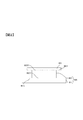
- FIG. 2 is a diagram schematically showing a cross section of the holding portion 85 in a plane parallel to the traveling direction of the plasma flow 43.
- the holding unit 85 includes a first holding unit 81 and a second holding unit 82.
- the first holding part 81 is made of a conductive material and is a plate-like member made of, for example, stainless steel.
- the second holding part 82 is attached to the surface 811 of the first holding part 81, that is, the surface exposed to the plasma flow by an attaching part (not shown). Note that the second holding portion 82 may be placed on the surface 811 of the first holding portion 81 without using the attachment portion.
- the material of the second holding portion 82 may be, for example, an insulating material such as a resin, may be a conductive material, or may be a semiconductive material, but it can more reliably suppress abnormal discharge. From this viewpoint, an insulating material is preferable.
- the semiconductivity means the property of a material having an electric conductivity of 10 ⁇ 6 to 10 5 (S / m), and the insulating property means an electric conductivity smaller than that of the semiconductive material.
- the term “conductivity” refers to the property of a material having an electric conductivity higher than that of a semiconductive material.
- the second holding portion 82 is formed in a columnar shape, for example, and the object 80 is attached to the second surface 822 opposite to the first surface 821 attached to the first holding portion 81 by an attaching portion (not shown). Note that the object 80 may be placed on the second surface 822 of the second holding portion 82 without using the attachment portion.
- the first surface 821 of the second holding portion 82 attached to the first holding portion 81 and the second surface 822 when the object 80 is attached are cathode material ions in the plasma flow. Not exposed to.
- the object 80 is attached so that at least the peripheral edge 801 of the object 80 does not overlap the second surface 822. In other words, the object 80 is attached to the second holding portion 82 so that the entire peripheral edge portion 801 protrudes from the second holding portion 82.
- the object 80 is held by the first holding part 81 via the second holding part 82 with the peripheral edge 801 of the object 80 being entirely separated from the surface 811 of the first holding part 81.
- a negative voltage is applied from the voltage source 51 to the first holding unit 81.
- abnormal discharge occurs between the object 80 and the first holding part 81. Is suppressed from occurring.
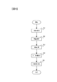
- step S ⁇ b> 1 the object 80 is held by the holding unit 85 inside the film forming chamber 70 while the peripheral edge 801 of the object 80 and the first holding unit 81 are separated from each other.
- step S2 the inside of the film forming chamber 70 is depressurized.
- the valve is opened, the rotary pump is operated, and after a predetermined degree of vacuum is reached, the turbo molecular pump is operated to continue depressurization. That's fine. In this way, the degree of vacuum inside the film forming chamber 70 can be easily controlled within a predetermined range.
- step S3 after reaching a predetermined degree of vacuum, film formation is started.
- a bias voltage is applied to the holding unit 85 by the voltage source 51.
- Arc discharge is generated in the discharge part 10.
- a current is applied in a state where the plasma generation trigger 15 is brought close to the surface of the target 11, and the arc discharge is generated between the object 80 and the contact portion 14 as described above.
- the plasma flow generated by the arc discharge is selected by the filter unit 20, the plasma flow 43 is irradiated onto the object 80, and a film is formed on the surface of the object 80.
- step S4 after forming a desired film, the shutter 60 is closed and the current application to the plasma generation trigger 15 is stopped to stop the arc discharge, thereby stopping the film formation.
- step S ⁇ b> 5 the object 80 on which the film is formed is taken out from the film formation chamber 70.
- the holding unit 85 holds at least the peripheral portion 801 of the object 80 and the holding unit 85, holds the object 80, and applies the voltage to the holding unit 85 by the ion plating method.
- a film is formed on the object 80. Accordingly, it is possible to suppress the occurrence of abnormal discharge between the object 80 and the holding unit 85 during the film forming process, and thus film formation in which the energy of the cathode material ions is controlled is possible.
- the holding unit 85 holds the object 80 by the second holding unit 82 disposed between the first holding unit 81 and the object 80. Therefore, since the peripheral part 801 of the target object 80 and the 1st holding
- the holding unit 85 may include a plurality of second holding units 82. Also in this case, the peripheral part 801 of the target object 80 and the first holding part 81 are separated from each other by attaching the target object 80 to the plurality of second holding parts 82, avoiding the peripheral part 801 of the target object 80. The object 80 is held.
- the plurality of second holding portions 82 may be made of the same material or different materials. Further, the plurality of second holding portions 82 may be placed side by side in the horizontal direction in FIG. 2 or may be stacked and placed in the vertical direction in FIG.
- each second holding portion 82 is formed in a weight shape, and the object is formed at the apex of the weight. 80 may be supported. Also in this case, the contact point between the apex of the second holding unit 82 and the object 80 is not exposed to the cathode material ions in the plasma flow.
- FIG. 4 is a diagram schematically showing a cross section of the holding portion 85 in the second embodiment.
- FIG. 4 is a cross section of the holding portion 85 in a plane parallel to the traveling direction of the plasma flow 43, and the plasma flow 53 flows from the upper side of the drawing to the holding portion 85.
- the holding portion 85 is a member made of, for example, stainless steel.
- the projecting portion 852 is formed in a columnar shape, for example, and the object 80 is attached to the upper surface (projecting portion surface 853) by an attaching portion (not shown). Note that the object 80 may be placed on the protruding portion surface 853 without using the attachment portion.
- the protruding portion surface 853 to which the object 80 is attached is not exposed to the cathode material ions in the plasma flow
- the area of the protruding portion surface 853 of the holding portion 85 is made smaller than the area of the portion occupied by the peripheral portion 801 of the object 80.
- the object 80 is attached so that at least the peripheral edge 801 of the object 80 does not overlap the protrusion surface 853. That is, the object 80 is attached to the holding portion 85 so that the entire peripheral edge portion 801 protrudes from the protruding portion surface 853.
- the object 80 is held by the holding unit 85 in a state where the peripheral edge 801 of the object 80 is separated from the surface 851 of the holding unit 85 throughout.
- the case where one protrusion 852 is formed in the holding portion 85 has been described as an example, but a plurality of protrusions 852 may be formed in the holding portion 85. Also in this case, the object 80 is attached to the plurality of protrusions 852 while avoiding the peripheral edge 801 of the object 80, thereby separating the peripheral edge 801 of the object 80 and the holding part 85, so that the object 80 is separated. Hold.
- the protrusion 852 is not limited to a columnar shape, and may be formed in a weight shape or a frustum shape, for example.
- each protruding portion 852 may be formed in a weight shape, and the object 80 may be supported at the apex of the weight. Also in this case, the contact point between the apex of the protrusion 852 and the object 80 is not exposed to the cathode material ions in the plasma flow.
- the holding portion 85 has a protrusion 852 in which at least a part of the surface 851 facing the object 80 protrudes toward the object 80, and the protrusion 852 comes into contact with the object 80, thereby Hold.
- an amorphous carbon film is formed on the object 80 using a carbon sintered body in which Ti is dispersed as the target 11.
- a Ti-containing tetrahead amorphous carbon (ta-C: Ti) film is formed on the object 80 as the amorphous carbon film.
- the film forming rate is 0.48 nm / second, and a pulse voltage of ⁇ 1980 V is applied to the first holding unit 81 with a duty ratio of 2%.
- chloroprene rubber is used as the material of the object 80.
- FIG. 5A shows a change in the value of a current flowing through the power supply circuit that applies a negative voltage to the first holding unit 81 in the first embodiment.
- the horizontal axis indicates the elapsed time (seconds) from the start of applying a negative voltage to the first holding unit 81
- the vertical axis indicates the current value (A) flowing through the power supply circuit.
- FIG. 5B shows a power supply circuit for applying a negative voltage to the first holding unit 81 in the comparative example in which the object 80 made of chloroprene rubber is directly attached to the first holding unit 81 without using the second holding unit 82. The change of the electric current value which flows through is shown.
- Example 2 In Example 2, a polycarbonate resin is used as the material of the object 80.
- FIG. 6A shows a change in the value of a current flowing through the power supply circuit that applies a negative voltage to the first holding unit 81 in the second embodiment. Also in FIG. 6, as in FIG. 5, the horizontal axis indicates the elapsed time (seconds) from the start of applying the negative voltage to the first holding unit 81, and the vertical axis indicates the current value (A ).
- FIG. 6B shows a power supply circuit that applies a negative voltage to the first holding unit 81 in the comparative example in which the object 80 made of polycarbonate is directly attached to the first holding unit 81 without using the second holding unit 82. The change of the flowing current value is shown.
- Example 3 In Example 3, polyethylene terephthalate resin is used as the material of the object 80.
- FIG. 7A shows a change in the value of a current flowing through the power supply circuit that applies a negative voltage to the first holding unit 81 in the second embodiment.
- the horizontal axis indicates the elapsed time (seconds) from the start of applying the negative voltage to the first holding unit 81, and the vertical axis indicates the current flowing through the power supply circuit. Value (A) is shown.
- the first holding part 81 is negative.
- the change of the electric current value which flows through the power supply circuit which applies a voltage is shown.
- the peripheral edge 801 of the object 80 and the surface 811 of the first holding part 81 are separated from each other.
- the occurrence of a sudden increase / decrease in the current value is suppressed, or even if the increase / decrease in the current value occurs, it is suppressed from being repeated. That is, the occurrence of abnormal discharge from the object 80 to the first holding unit 81 is suppressed.
- the sudden increase in the current value is caused by abnormal discharge from the object 80 to the first holding unit 81.
- the sudden decrease in the current value is due to the operation of the protection circuit of the power supply circuit that applies negative charges due to the sudden increase in the current value, and the voltage application to the first holding unit 81 is stopped. That is, abnormal discharge from the object 80 that causes a sudden increase or decrease in the current value due to the object 80 being held in a state where the peripheral edge 801 of the object 80 and the first holding part 81 are separated from each other. It turns out that generation
- Example 4 an amorphous carbon film is formed on the target 80 using a carbon sintered body in which Ti is dispersed as the target 11.
- a Ti-containing tetrahead amorphous carbon (ta-C: Ti) film is formed on the object 80 as the amorphous carbon film.
- the film forming rate is 0.48 nm / second, and a pulse voltage of ⁇ 1980 V is applied to the first holding unit 81 with a duty ratio of 2%.
- a Si wafer is used as the object 80.
- FIG. 8 shows the distance between the peripheral edge 801 of the object 80 and the first holding part 81 by 0.1 mm, 0.2 mm, 0.3 mm, 0.5 mm, 1.0 mm, 2.0 mm. It is a figure which shows the stress of the film of the target object 80 obtained when it sets to 0 mm and 7.0 mm. As shown in FIG. 8, the stress of the coating also changes as the distance between the peripheral edge 801 of the object 80 and the first holding part 81 changes. Thereby, the film-forming process which controlled the energy which a cathode material ion has by the holding
- maintenance part 81 increases, the absolute value of the value of the stress of a film will also increase.
- the smaller the distance between the peripheral edge 801 of the object 80 and the first holding part 81 the smaller the stress in which the energy of the cathode material ions is controlled.
- the distance between the peripheral edge 801 of the object 80 and the first holding part 81 is too small, abnormal discharge may occur, so it is preferable to select an appropriate distance.
- the present invention is not limited to the above-described embodiments, and other forms conceivable within the scope of the technical idea of the present invention are also included in the scope of the present invention. .
- Control unit 70 ... Deposition chamber, 80 ... object, 81 ... first holding part, 82 ... second holding part, 85 ... holding part, 100: film forming apparatus, 801: peripheral edge, 811 ... surface, 821 ... first surface, 822 ... second surface, 852 ... projection, 853 ... Projection surface
Landscapes
- Engineering & Computer Science (AREA)
- Chemical & Material Sciences (AREA)
- Physics & Mathematics (AREA)
- Plasma & Fusion (AREA)
- Spectroscopy & Molecular Physics (AREA)
- Chemical Kinetics & Catalysis (AREA)
- Materials Engineering (AREA)
- Mechanical Engineering (AREA)
- Metallurgy (AREA)
- Organic Chemistry (AREA)
- Physical Vapour Deposition (AREA)
- Plasma Technology (AREA)
Abstract
対象物に被膜を成膜する成膜方法は、保持部を用いて、対象物の少なくとも周縁部と保持部との間を離間させて、対象物を保持し、保持部に電圧を印加しながらイオンプレーティング法により対象物に被膜を成膜する。
Description
本発明は、成膜方法および成膜装置に関する。
従来から、イオンプレーティング法により対象物に被膜を形成する成膜処理を行う装置が知られている(たとえば特許文献1)。このような装置を用いる際、被膜の諸特性を制御するため、対象物を保持する部材に負電圧を印加することがある。このとき、対象物が絶縁性を有していると、対象物に飛来したイオンに起因して対象物の表面に正の電荷が蓄積されていく。そして、特に対象物の端部(周縁部)に電荷が集中して、対象物の端部と対象物を保持する部材との間の空間が絶縁破壊を起こして異常放電を生じることがある。異常放電は、対象物にダメージを与えることがあるため、その発生を抑制することが好ましい。
第1の態様によると、対象物に被膜を成膜する成膜方法は、保持部を用いて、前記対象物の少なくとも周縁部と前記保持部との間を離間させて、前記対象物を保持し、前記保持部に電圧を印加しながらイオンプレーティング法により前記対象物に前記被膜を成膜する。
第2の態様によると、対象物に被膜を成膜するための成膜装置は、前記対象物の少なくとも周縁部との間を離間させて、前記対象物を保持する保持部と、前記保持部に電圧を印加しながらイオンプレーティング法により前記対象物に前記被膜を成膜する成膜処理部と、を有する。
第2の態様によると、対象物に被膜を成膜するための成膜装置は、前記対象物の少なくとも周縁部との間を離間させて、前記対象物を保持する保持部と、前記保持部に電圧を印加しながらイオンプレーティング法により前記対象物に前記被膜を成膜する成膜処理部と、を有する。
<第1の実施の形態>
図面を参照して第1の実施の形態に係る成膜装置について説明する。
図1は、第1の実施の形態による成膜装置100の要部構成を説明する図である。成膜装置100は、イオンプレーティング法により、プラズマや真空放電でイオン化または励起状態にした原料を電場によって加速し、基板等の対象物80に真空蒸着させて被膜を形成する成膜処理を行う。以下の説明においては、成膜装置100は、イオンプレーティング法として、フィルタードカソーディックバキュームアーク(FCVA)法により成膜処理を行う場合を例に挙げる。なお、成膜装置100は、イオンプレーティング法として、アークイオンプレーティング法等の手法を用いて成膜処理を行うものであってもよい。
図面を参照して第1の実施の形態に係る成膜装置について説明する。
図1は、第1の実施の形態による成膜装置100の要部構成を説明する図である。成膜装置100は、イオンプレーティング法により、プラズマや真空放電でイオン化または励起状態にした原料を電場によって加速し、基板等の対象物80に真空蒸着させて被膜を形成する成膜処理を行う。以下の説明においては、成膜装置100は、イオンプレーティング法として、フィルタードカソーディックバキュームアーク(FCVA)法により成膜処理を行う場合を例に挙げる。なお、成膜装置100は、イオンプレーティング法として、アークイオンプレーティング法等の手法を用いて成膜処理を行うものであってもよい。
成膜装置100は、放電部10と、フィルタ部20と、測定部30と、スキャン部40と、制御部50と、成膜室70とを備える。
放電部10の内部には、ターゲット11が載置される。ターゲット11は、例えば、炭素、チタン、アルミニウム、クロム等の単一の原料からなる材料であってよい。また、ターゲット11は、上述した単一の原料に金属元素、または非金属元素が添加された複数の原料からなる複合材料であってよい。本実施の形態では、ターゲット11には、炭素とチタンとが混合されている場合を例に挙げる。本実施の形態では、ターゲット11は電気的に接地されている。
放電部10の内部には、ターゲット11が載置される。ターゲット11は、例えば、炭素、チタン、アルミニウム、クロム等の単一の原料からなる材料であってよい。また、ターゲット11は、上述した単一の原料に金属元素、または非金属元素が添加された複数の原料からなる複合材料であってよい。本実施の形態では、ターゲット11には、炭素とチタンとが混合されている場合を例に挙げる。本実施の形態では、ターゲット11は電気的に接地されている。
放電部10は、プラズマ発生トリガ15およびトリガ移動部16を有する。プラズマ発生トリガ15は、先端が尖った形状である接触部14を有する。高電圧である接触部14をターゲット11の表面に近接させることにより、ターゲット11に対してアーク放電を生じさせる。アーク放電により、ターゲット11からは、炭素とチタンとがプラズマ状態となり放出する。なお、トリガ移動部16は、ターゲット11に対する接触部14の位置を移動させる。接触部14の位置が移動することにより、接触部14はターゲット11の表面の異なる位置に接触することができる。したがって、ターゲット11の異なる位置において、アーク放電を発生させることができる。
フィルタ部20は、放電部10に接続される。フィルタ部20は、湾曲した筒の外部表面に巻き付けられた巻線25を備える。巻線25はソレノイドコイルを形成してよい。巻線25に電流を流すことにより、フィルタ部20の内部において、湾曲した筒の内部に沿った磁場を印加することができる。また、巻線25に流す電流量を制御することにより、磁場の大きさを制御することができる。これにより、磁場の大きさを制御して、イオン価数およびイオン質量に基づきイオンの流れを制御することができる。フィルタ部20は、例えばプラズマ流フィルタである。フィルタ部20は、湾曲した筒形状である。フィルタ部20は、プラズマ流に磁場を印加して、プラズマ流の流れを制御する。
フィルタ部20は、プラズマ流に含まれるイオンのイオン価数およびイオン質量に基づき、放電部10から発生したプラズマ流の方向を変える。本実施の形態では、フィルタ部20は、予め定められたイオン種である炭素イオンおよびチタンイオンの流れを通過させる(プラズマ流29)。しかし、フィルタ部20は、予め定められたイオン種以外のイオンからなるプラズマ流の方向を変えて、当該プラズマ流を湾曲した筒の内部に衝突させる(プラズマ流27)。したがって、フィルタ部20は、プラズマ流27をフィルタ部20内で遮ることができる。
測定部30は、たとえば、プラズマの輝線スペクトルを分光することで、複数のイオンのスペクトル強度比を特定する発光分光光度計である。測定部30は、発光分光光度を測定することにより、プラズマ流中における陰極物質イオンの存在比を測定する。測定部30は、プラズマ中の対象イオン種による吸収スペクトルを測定するものであってよい。測定部30は、フィルタ部20に接続されて設けられる。複数のイオンに基づくスペクトル強度比からプラズマ流中におけるイオンの存在比を算出することができる。測定部30によってプラズマ流を観測しつつ、プラズマ流を対象物80に照射することにより、対象物80に成膜される元素の組成比を特定し制御することができる。本実施の形態においては、炭素イオンおよびチタンイオンに固有の波長スペクトル強度を観測することにより、対象物80に成膜される炭素とチタンの組成比を特定し制御する。なお、本明細書における組成比とは、特に断らない限り原子数比を指すものとする。
本実施の形態の測定部30は、フィルタ部20において、比較的放電部10に近い位置に備えられるが、測定部30は、フィルタ部20において、比較的スキャン部40に近い位置に備えられてもよい。また、測定部30はスキャン部40に備えられてもよい。測定部30をスキャン部40に備える場合には、フィルタ部20に設ける巻線25を隙間なく配置することができるので、測定部30をフィルタ部20に備える場合と比較して、より均一に磁場を発生させることができる。なお、測定部30としては、発光分光光度計の他に、紫外~可視域の吸収分光光度計、ラマン分光光度計、CARS分光光度計、ラングミュアプローブ等を用いることができる。
スキャン部40は、フィルタ部20と成膜室70との間に設けられる。フィルタ部20を通過したプラズマ流はスキャン部40に入る。スキャン部40によりスキャンされたプラズマ流は成膜室70に導かれる。
スキャン部40は、プラズマ流と交差する方向において印加する磁界の大きさを変化させることで、対象物80にプラズマ流が照射される向きを制御する。たとえば、スキャン部40において、プラズマ流に対して磁界を印加しない場合には、プラズマ流はスキャン部40で偏向することなしに対象物80にプラズマ流が照射される(プラズマ流43)。また、スキャン部40において、プラズマ流と交差する方向において磁界を印加することにより、対象物80におけるプラズマ流の照射位置を制御することができ、それにより、対象物80における成膜位置や成膜厚さを調節することができる。スキャン部40のスキャンを制御することにより、対象物80に形成される被膜を均一にすることができる。また、スキャン部40において、比較的大きな磁界を印加することにより、プラズマ流の偏向を大きくして、プラズマ流を対象物80に照射しないようにすることもできる(プラズマ流45)。
なお、本実施の形態においては、成膜装置100は、フィルタ部20と成膜室70との間にスキャン部40を備えるが、スキャン部40を備えていなくてもよい。
なお、本実施の形態においては、成膜装置100は、フィルタ部20と成膜室70との間にスキャン部40を備えるが、スキャン部40を備えていなくてもよい。
制御部50は、測定部30からの情報に基づき、放電部10のプラズマ発生トリガ15およびトリガ移動部16、巻線25の電流量、スキャン部40の磁界、ならびに後述される成膜室70に設けられたシャッタ部60の位置を制御する。制御部50は、測定部30が測定した、対象物80に向かうプラズマ流中に存在する複数の元素の組成比に基づいて、対象物80に到達するプラズマ流の量を制御する。
具体的には、制御部50は、対象物80に向かうプラズマ流中に存在する複数の元素の組成比の時間変動情報を、測定部30による測定結果に基づき算出する。制御部50は、この時間変動情報に基づいて、対象物80に到達するプラズマ流の量を制御する。たとえば、制御部50は、フィルタ部20の磁場の大きさを調整することにより、対象物80に照射されるプラズマ流の偏向状態を調整する。これにより、複数の元素が予め定められた構成比で含まれる膜が、対象物80に成膜される。
制御部50は、成膜室70と電気的に接続された電圧源51を制御して、成膜室70内に設けられる保持部85にバイアス電圧を印加する。ここで、バイアス電圧の電圧源51として直流電圧源を示しているが、交流電圧源であってもよい。保持部85にバイアス電圧を印加することで、対象物80の表面に照射されるイオンのエネルギーを抑制し、成長中の被膜表面から被膜内部への入射イオンの拡散、均一な被膜を形成できる。
成膜室70は真空容器であり、シャッタ部60および保持部85を備える。本実施の形態では、シャッタ部60は、対象物80に向かうプラズマ流を遮蔽するか否かを切り替える機械的シャッタである。元素の組成比が予め定められた範囲内となった状態で機械的シャッタを開き、対象物80に所定の厚さの膜が形成されたらシャッタを閉じることで、対象物80に適切に被膜を形成することができる。なお、成膜室70には、ロードロックチャンバー(図示略)が接続されていてもよい。ロードロックチャンバーから対象物80を出し入れすることにより、成膜室70の内部は通常真空状態に保たれるので、成膜室70への不純物の混入を抑制できる。成膜室70には、たとえばバルブや、ターボ分子ポンプやロータリーポンプ等の真空装置(不図示)が接続され、成膜室70内の真空度(減圧度)が制御される。
保持部85は、成膜室70内において、対象物80を保持する。なお、保持部85については、詳細な説明を後に行う。
保持部85は、成膜室70内において、対象物80を保持する。なお、保持部85については、詳細な説明を後に行う。
次に、図2を参照して保持部85について説明する。図2は、プラズマ流43の進行方向と平行な面における保持部85の断面を模式的に示す図である。図2においては、プラズマ流43が紙面上部から保持部85に向かって流れる。
保持部85は、第1保持部81と第2保持部82とを有する。第1保持部81は、導電性材料で構成され、たとえばステンレス鋼等からなる板状の部材である。第1保持部81の表面811、すなわちプラズマ流に曝される側の面には、第2保持部82が図示しない取付部によって取り付けられる。なお、第2保持部82は、取付部を用いず第1保持部81の表面811に載置されてもよい。第2保持部82の材料は、たとえば樹脂等の絶縁性を有する材料であってよく、導電性材料であってよく、半導電性材料であってもよいが、異常放電をより確実に抑制するという観点では絶縁材料とすることが好ましい。なお、本明細書における半導電性とは、電気伝導率が10-6~105(S/m)である材料の性質をいい、絶縁性とは、半導電性材料よりも小さい電気伝導率を有する材料の性質をいい、導電性とは、半導電性材料よりも大きい電気伝導率を有する材料の性質をいう。第2保持部82は、たとえば柱状に形成され、第1保持部81に取り付けられる第1面821とは反対側の第2面822には、対象物80が図示しない取付部によって取り付けられる。なお、対象物80は、取付部を用いず第2保持部82の第2面822に載置されてもよい。第2保持部82において、第1保持部81に取り付けられる第2保持部82の第1面821と、対象物80が取り付けられた場合の第2面822とは、プラズマ流中の陰極物質イオンに曝されない。
保持部85は、第1保持部81と第2保持部82とを有する。第1保持部81は、導電性材料で構成され、たとえばステンレス鋼等からなる板状の部材である。第1保持部81の表面811、すなわちプラズマ流に曝される側の面には、第2保持部82が図示しない取付部によって取り付けられる。なお、第2保持部82は、取付部を用いず第1保持部81の表面811に載置されてもよい。第2保持部82の材料は、たとえば樹脂等の絶縁性を有する材料であってよく、導電性材料であってよく、半導電性材料であってもよいが、異常放電をより確実に抑制するという観点では絶縁材料とすることが好ましい。なお、本明細書における半導電性とは、電気伝導率が10-6~105(S/m)である材料の性質をいい、絶縁性とは、半導電性材料よりも小さい電気伝導率を有する材料の性質をいい、導電性とは、半導電性材料よりも大きい電気伝導率を有する材料の性質をいう。第2保持部82は、たとえば柱状に形成され、第1保持部81に取り付けられる第1面821とは反対側の第2面822には、対象物80が図示しない取付部によって取り付けられる。なお、対象物80は、取付部を用いず第2保持部82の第2面822に載置されてもよい。第2保持部82において、第1保持部81に取り付けられる第2保持部82の第1面821と、対象物80が取り付けられた場合の第2面822とは、プラズマ流中の陰極物質イオンに曝されない。
対象物80の少なくとも周縁部801が第2面822と重複しないように対象物80が取り付けられる。すなわち、対象物80は、周縁部801の全体が、第2保持部82からはみ出した状態となるように第2保持部82に取り付けられる。これにより、対象物80の周縁部801は全体にわたって第1保持部81の表面811と離間された状態で、対象物80は第2保持部82を介して第1保持部81に保持される。 電圧源51からは第1保持部81に負電圧が印加される。上述したように、対象物80の周縁部801と第1保持部81との間が離間した状態で対象物80が保持されるので、対象物80と第1保持部81との間で異常放電が発生することが抑制される。
図3に示すフローチャートを参照して、本実施の形態の成膜装置100による成膜処理の手順を説明する。
ステップS1では、成膜室70内部の保持部85で、対象物80の周縁部801と第1保持部81との間を離間させた状態で対象物80を保持する。
ステップS2では、成膜室70内部を減圧する。この時、例えば、減圧の初期段階ではターボ分子ポンプは停止させた状態で、バルブを開き、ロータリーポンプを作動させ、所定の真空度になってから、ターボ分子ポンプを作動させて、引き続き減圧すればよい。このようにすることで、成膜室70内部の真空度を所定の範囲に容易に制御できる。
ステップS1では、成膜室70内部の保持部85で、対象物80の周縁部801と第1保持部81との間を離間させた状態で対象物80を保持する。
ステップS2では、成膜室70内部を減圧する。この時、例えば、減圧の初期段階ではターボ分子ポンプは停止させた状態で、バルブを開き、ロータリーポンプを作動させ、所定の真空度になってから、ターボ分子ポンプを作動させて、引き続き減圧すればよい。このようにすることで、成膜室70内部の真空度を所定の範囲に容易に制御できる。
ステップS3では、所定の真空度に到達後、成膜を開始する。このとき、電圧源51により、保持部85にバイアス電圧を印加する。放電部10にアーク放電を生じさせる。アーク放電を生じさせる際には、プラズマ発生トリガ15をターゲット11の表面に近接させた状態で電流を印加し、上記のように、対象物80と接触部14との間にアーク放電を生じさせる。アーク放電により発生したプラズマ流は、フィルタ部20によって選別されプラズマ流43が対象物80に照射され、対象物80の表面に被膜が成膜される。
ステップS4では、所望の被膜を形成した後、シャッタ60を閉じると共にプラズマ発生トリガ15への電流印加を停止してアーク放電を停止することで、成膜を停止する。ステップS5では、被膜が成膜された対象物80を成膜室70から取り出す。
上述した第1の実施の形態によれば、次の作用効果が得られる。
(1)保持部85は、対象物80の少なくとも周縁部801と保持部85との間を離間させて、対象物80を保持し、保持部85に電圧を印加しながらイオンプレーティング法により対象物80に被膜を成膜する。これにより、成膜処理のときに対象物80と保持部85との間に異常放電が発生することを抑制することができるので、陰極物質イオンのエネルギーが制御された成膜が可能となる。
(1)保持部85は、対象物80の少なくとも周縁部801と保持部85との間を離間させて、対象物80を保持し、保持部85に電圧を印加しながらイオンプレーティング法により対象物80に被膜を成膜する。これにより、成膜処理のときに対象物80と保持部85との間に異常放電が発生することを抑制することができるので、陰極物質イオンのエネルギーが制御された成膜が可能となる。
(2)保持部85は、第1保持部81と対象物80との間に配置された第2保持部82によって対象物80を保持する。これにより、対象物80の周縁部801と第1保持部81との間を離間させることができるので、成膜処理中の異常放電の発生を抑制できる。
上述した第1の実施の形態を以下のように変形できる。
(1)保持部85が1個の第2保持部82を有する場合を例に挙げて説明を行ったが、保持部85は複数個の第2保持部82を有してもよい。この場合も、複数の第2保持部82には、対象物80の周縁部801を避けて対象物80を取り付けることにより、対象物80の周縁部801と第1保持部81とを離間させて対象物80を保持する。また、複数個の第2保持部82は、それぞれが同じ材料で構成されていてよいし、異なる材料で構成されていてもよい。また、複数個の第2保持部82は、図2の紙面横方向に並べて載置してもよいし、図2の紙面縦方向に積み重ねて載置してもよい。
(1)保持部85が1個の第2保持部82を有する場合を例に挙げて説明を行ったが、保持部85は複数個の第2保持部82を有してもよい。この場合も、複数の第2保持部82には、対象物80の周縁部801を避けて対象物80を取り付けることにより、対象物80の周縁部801と第1保持部81とを離間させて対象物80を保持する。また、複数個の第2保持部82は、それぞれが同じ材料で構成されていてよいし、異なる材料で構成されていてもよい。また、複数個の第2保持部82は、図2の紙面横方向に並べて載置してもよいし、図2の紙面縦方向に積み重ねて載置してもよい。
(2)第2保持部82が柱状に形成されるものに限定されず、たとえば錘状や錘台状に形成されてよい。特に、上記の変形例(1)のように複数の第2保持部82に対象物80を取り付ける場合には、各々の第2保持部82を錘状に形成し、錘の頂点にて対象物80を支持してもよい。この場合も、第2保持部82の頂点と対象物80との接触点はプラズマ流中の陰極物質イオンに曝されない。
<第2の実施の形態>
図面を参照して第2の実施の形態の成膜装置について説明する。以下の説明では、第1の実施の形態と同じ構成要素には同じ符号を付して相違点を主に説明する。特に説明しない点については、第1の実施の形態と同じである。本実施の形態では、対象物を保持する保持部が第2保持部を備えていない点が第1の実施の形態とは異なる。
図面を参照して第2の実施の形態の成膜装置について説明する。以下の説明では、第1の実施の形態と同じ構成要素には同じ符号を付して相違点を主に説明する。特に説明しない点については、第1の実施の形態と同じである。本実施の形態では、対象物を保持する保持部が第2保持部を備えていない点が第1の実施の形態とは異なる。
図4は、第2の実施の形態における保持部85の断面を模式的に示す図である。図4は、プラズマ流43の進行方向と平行な面における保持部85の断面であり、図の紙面上方から保持部85に向けてプラズマ流53が流れる。保持部85は、たとえばステンレス鋼等により作成される部材である。保持部85の表面851、すなわち保持部85に対象物80を取り付けた場合に対象物80と対向する面には、プラズマ流が到来する方向に向けて突出した突出部852が形成される。突出部852は、たとえば柱状に形成され、その上部の表面(突出部表面853)に対象物80が図示しない取付部によって取り付けられる。なお、対象物80は取付部を用いず突出部表面853に載置されてもよい。保持部85において、対象物80が取り付けられる突出部表面853は、プラズマ流中の陰極物質イオンに曝されない。
保持部85の突出部表面853の面積は、対象物80周縁部801が占める部分の面積に比べて小さく作製される。また、対象物80の少なくとも周縁部801が突出部表面853と重複しないように対象物80が取り付けられる。すなわち、対象物80は、周縁部801の全体が、突出部表面853からはみ出した状態となるように保持部85に取り付けられる。これにより、対象物80の周縁部801は全体にわたって保持部85の表面851と離間された状態で、対象物80は保持部85に保持される。
なお、上述した説明では、保持部85に1個の突出部852が形成される場合を例に挙げたが、保持部85には複数個の突出部852が形成されてよい。この場合も、複数の突出部852には、対象物80の周縁部801を避けて対象物80を取り付けることにより、対象物80の周縁部801と保持部85とを離間させて対象物80を保持する。
また、突出部852が柱状に形成されるものに限定されず、たとえば錘状や錘台状に形成されてよい。特に、保持部85に複数の突出部852が形成される場合には、各々の突出部852を錘状に形成し、錘の頂点にて対象物80を支持してもよい。この場合も、突出部852の頂点と対象物80との接触点はプラズマ流中の陰極物質イオンに曝されない。
以上で説明した第2の実施の形態によれば、第1の実施の形態で得られた(1)の作用効果に加えて、以下の作用効果が得られる。
保持部85は、対象物80と対向する表面851の少なくとも一部が対象物80へ向けて突出する突出部852を有し、突出部852が対象物80と接触することにより、対象物80を保持する。これにより、対象物80の周縁部801と表面851との間を離間させることができるので、成膜処理中の異常放電の発生を抑制できる。
保持部85は、対象物80と対向する表面851の少なくとも一部が対象物80へ向けて突出する突出部852を有し、突出部852が対象物80と接触することにより、対象物80を保持する。これにより、対象物80の周縁部801と表面851との間を離間させることができるので、成膜処理中の異常放電の発生を抑制できる。
次に、保持部85の実施例について説明する。以下の各実施例においては、ターゲット11としてTiが分散されたカーボン焼結体を用いて、対象物80にアモルファスカーボン膜を成膜する。アモルファスカーボン膜として、Ti含有テトラヘッドアモルファスカーボン(ta-C:Ti)膜を対象物80に成膜する。成膜速度を0.48nm/秒とし、第1保持部81にはデューティー比2%で-1980Vのパルス電圧が印加される。
[実施例1]
実施例1においては、対象物80の材料としてクロロプレンゴムを使用する。
図5(a)は、実施例1において第1保持部81に負電圧を印加する電源回路を流れる電流値の変化を示す。なお、図5において、横軸は第1保持部81に負電圧の印加を開始してからの経過時間(秒)を示し、縦軸は電源回路を流れる電流値(A)を示す。
[比較例1]
図5(b)は、第2保持部82を介することなく第1保持部81にクロロプレンゴムからなる対象物80を直接取り付けた比較例において、第1保持部81に負電圧を印加する電源回路を流れる電流値の変化を示す。
[実施例1]
実施例1においては、対象物80の材料としてクロロプレンゴムを使用する。
図5(a)は、実施例1において第1保持部81に負電圧を印加する電源回路を流れる電流値の変化を示す。なお、図5において、横軸は第1保持部81に負電圧の印加を開始してからの経過時間(秒)を示し、縦軸は電源回路を流れる電流値(A)を示す。
[比較例1]
図5(b)は、第2保持部82を介することなく第1保持部81にクロロプレンゴムからなる対象物80を直接取り付けた比較例において、第1保持部81に負電圧を印加する電源回路を流れる電流値の変化を示す。
[実施例2]
実施例2においては、対象物80の材料としてポリカーボネイト樹脂を使用する。
図6(a)は、実施例2において第1保持部81に負電圧を印加する電源回路を流れる電流値の変化を示す。なお、図6においても図5と同様に、横軸は第1保持部81に負電圧の印加を開始してからの経過時間(秒)を示し、縦軸は電源回路を流れる電流値(A)を示す。
[比較例2]
図6(b)は、第2保持部82を介することなく第1保持部81にポリカーボネイトからなる対象物80を直接取り付けた比較例において、第1保持部81に負電圧を印加する電源回路を流れる電流値の変化を示す。
実施例2においては、対象物80の材料としてポリカーボネイト樹脂を使用する。
図6(a)は、実施例2において第1保持部81に負電圧を印加する電源回路を流れる電流値の変化を示す。なお、図6においても図5と同様に、横軸は第1保持部81に負電圧の印加を開始してからの経過時間(秒)を示し、縦軸は電源回路を流れる電流値(A)を示す。
[比較例2]
図6(b)は、第2保持部82を介することなく第1保持部81にポリカーボネイトからなる対象物80を直接取り付けた比較例において、第1保持部81に負電圧を印加する電源回路を流れる電流値の変化を示す。
[実施例3]
実施例3においては、対象物80の材料としてポリエチレンテレフタレート樹脂を使用する。
図7(a)は、実施例2において第1保持部81に負電圧を印加する電源回路を流れる電流値の変化を示す。なお、図7においても図5や図6と同様に、横軸は第1保持部81に負電圧の印加を開始してからの経過時間(秒)を示し、縦軸は電源回路を流れる電流値(A)を示す。
[比較例3]
これに対して、図7(b)は、第2保持部82を介することなく第1保持部81にポリエチレンテレフタラートからなる対象物80を直接取り付けた比較例において、第1保持部81に負電圧を印加する電源回路を流れる電流値の変化を示す。
実施例3においては、対象物80の材料としてポリエチレンテレフタレート樹脂を使用する。
図7(a)は、実施例2において第1保持部81に負電圧を印加する電源回路を流れる電流値の変化を示す。なお、図7においても図5や図6と同様に、横軸は第1保持部81に負電圧の印加を開始してからの経過時間(秒)を示し、縦軸は電源回路を流れる電流値(A)を示す。
[比較例3]
これに対して、図7(b)は、第2保持部82を介することなく第1保持部81にポリエチレンテレフタラートからなる対象物80を直接取り付けた比較例において、第1保持部81に負電圧を印加する電源回路を流れる電流値の変化を示す。
図5(a)、図6(a)、図7(a)に示すように、実施例1~3では、対象物80の周縁部801と第1保持部81の表面811とが離間した状態で対象物80が保持されることにより、電流値の急激な増減の発生が抑制されている、あるいは電流値の増減が発生したとしてもそれが繰り返されることが抑制されている。すなわち、対象物80から第1保持部81への異常放電の発生が抑制されている。これに対して、図5(b)、図6(b)、図7(b)に示す比較例においては、電流値の急激な増減が繰り返される。電流値の急激な増加は、対象物80から第1保持部81へ異常放電が生じたことが原因である。電流値の急激な低下は、上記の電流値の急激な増加により負電荷を印加する電源回路の保護回路が作動し、第1保持部81への電圧印加が停止されたことによるものである。
すなわち、対象物80の周縁部801と第1保持部81とが離間した状態で対象物80が保持されることにより、電流値に急激な増減が発生する原因となる対象物80からの異常放電の発生を抑制することができることがわかる。
すなわち、対象物80の周縁部801と第1保持部81とが離間した状態で対象物80が保持されることにより、電流値に急激な増減が発生する原因となる対象物80からの異常放電の発生を抑制することができることがわかる。
次に、実施例4により対象物80の周縁部801と第1保持部81との間の間隔と、対象物80に成膜される被膜の応力との関係について説明する。
[実施例4]
実施例4においては、ターゲット11としてTiが分散されたカーボン焼結体を用いて、対象物80にアモルファスカーボン膜を成膜する。アモルファスカーボン膜として、Ti含有テトラヘッドアモルファスカーボン(ta-C:Ti)膜を対象物80に成膜する。成膜速度を0.48nm/秒とし、第1保持部81にはデューティー比2%で-1980Vのパルス電圧が印加される。対象物80としてSiウエハを使用する。
[実施例4]
実施例4においては、ターゲット11としてTiが分散されたカーボン焼結体を用いて、対象物80にアモルファスカーボン膜を成膜する。アモルファスカーボン膜として、Ti含有テトラヘッドアモルファスカーボン(ta-C:Ti)膜を対象物80に成膜する。成膜速度を0.48nm/秒とし、第1保持部81にはデューティー比2%で-1980Vのパルス電圧が印加される。対象物80としてSiウエハを使用する。
図8は、対象物80の周縁部801と第1保持部81との間の間隔を、0.1mm、0.2mm、0.3mm、0.5mm、1.0mm、2.0mm、4.0mm、7.0mmに設定した場合に得られる対象物80の被膜の応力を示す図である。図8に示すように、対象物80の周縁部801と第1保持部81との間の間隔の変化に伴って、被膜の応力も変化する。これにより、本実施の形態による保持部85により、陰極物質イオンが有するエネルギーを制御した成膜処理が可能となる。また、対象物80の周縁部801と第1保持部81との間の間隔が増加すると、被膜の応力の値の絶対値も増加する。すなわち、対象物80の周縁部801と第1保持部81との間の間隔が小さいほど、陰極物質イオンのエネルギーが制御された応力の小さな成膜が可能になる。ただし、対象物80の周縁部801と第1保持部81との間の間隔が小さ過ぎると、異常放電が発生するおそれがあるので、適当な間隔を選択することが好ましい。
本発明の特徴を損なわない限り、本発明は上記実施の形態に限定されるものではなく、本発明の技術的思想の範囲内で考えられるその他の形態についても、本発明の範囲内に含まれる。
次の優先権基礎出願の開示内容は引用文としてここに組み込まれる。
日本国特許出願2018年第046805号(2018年3月14日出願)
日本国特許出願2018年第046805号(2018年3月14日出願)
50…制御部、70…成膜室、
80…対象物、81…第1保持部、
82…第2保持部、85…保持部、
100…成膜装置、801…周縁部、
811…表面、821…第1面、
822…第2面、852…突出部、
853…突出部表面
80…対象物、81…第1保持部、
82…第2保持部、85…保持部、
100…成膜装置、801…周縁部、
811…表面、821…第1面、
822…第2面、852…突出部、
853…突出部表面
Claims (16)
- 対象物に被膜を成膜する成膜方法であって、
保持部を用いて、前記対象物の少なくとも周縁部と前記保持部との間を離間させて、前記対象物を保持し、
前記保持部に電圧を印加しながらイオンプレーティング法により前記対象物に前記被膜を成膜する、成膜方法。 - 請求項1に記載の成膜方法において、
前記保持部は、前記対象物と対向する面の少なくとも一部が前記対象物へ向けて突出する突出部を有し、前記突出部が前記対象物と接触することにより、前記対象物を保持する、成膜方法。 - 請求項2に記載の成膜方法において、
前記突出部と前記対象物とが接触する領域は、陰極物質イオンに曝されない、成膜方法。 - 請求項1に記載の成膜方法において、
前記保持部と前記対象物との間に配置された第2の保持部によって、前記対象物を保持する、成膜方法。 - 請求項4に記載の成膜方法において、
前記第2の保持部は、絶縁性を有する、成膜方法。 - 請求項4または5に記載の成膜方法において、
前記第2の保持部と前記対象物とが接触する領域は、陰極物質イオンに曝されない、成膜方法。 - 請求項4から6までのいずれか一項に記載の成膜方法において、
前記第2の保持部と前記保持部とが接触する領域は、陰極物質イオンに曝されない、成膜方法。 - 請求項1から7までのいずれか一項に記載の成膜方法において、
前記対象物は、絶縁性を有する、成膜方法。 - 請求項1から8までのいずれか一項に記載の成膜方法において、
前記対象物は、樹脂材料を含む、成膜方法。 - 請求項1から9までのいずれか一項に記載の成膜方法において、
前記対象物は、可撓性を有する、成膜方法。 - 請求項1から10までのいずれか一項に記載の成膜方法において、
前記イオンプレーティング法として、フィルタードカソーディックバキュームアーク法を用いる、成膜方法。 - 請求項1から11までのいずれか一項に記載の成膜方法において、
前記被膜は、アモルファスカーボン膜である、成膜方法。 - 対象物に被膜を成膜するための成膜装置であって、
前記対象物の少なくとも周縁部との間を離間させて、前記対象物を保持する保持部と、
前記保持部に電圧を印加しながらイオンプレーティング法により前記対象物に前記被膜を成膜する成膜処理部と、を有する成膜装置。 - 請求項13に記載の成膜装置において、
前記保持部は、前記対象物と対向する面の少なくとも一部が前記対象物へ向けて突出する突出部を有し、
前記突出部が前記対象物と接触することにより、前記保持部は前記対象物を保持する成膜装置。 - 請求項14に記載の成膜装置において、
前記保持部と前記対象物との間に配置された第2の保持部をさらに備え、
前記第2の保持部を介して、前記保持部は前記対象物を保持する成膜装置。 - 請求項15に記載の成膜装置において、
前記第2の保持部は、絶縁性を有する成膜装置。
Applications Claiming Priority (2)
| Application Number | Priority Date | Filing Date | Title |
|---|---|---|---|
| JP2018-046805 | 2018-03-14 | ||
| JP2018046805A JP2021075734A (ja) | 2018-03-14 | 2018-03-14 | 成膜方法および成膜装置 |
Publications (1)
| Publication Number | Publication Date |
|---|---|
| WO2019176459A1 true WO2019176459A1 (ja) | 2019-09-19 |
Family
ID=67906632
Family Applications (1)
| Application Number | Title | Priority Date | Filing Date |
|---|---|---|---|
| PCT/JP2019/005883 Ceased WO2019176459A1 (ja) | 2018-03-14 | 2019-02-18 | 成膜方法および成膜装置 |
Country Status (2)
| Country | Link |
|---|---|
| JP (1) | JP2021075734A (ja) |
| WO (1) | WO2019176459A1 (ja) |
Citations (4)
| Publication number | Priority date | Publication date | Assignee | Title |
|---|---|---|---|---|
| JP2000343151A (ja) * | 1999-06-03 | 2000-12-12 | Komatsu Ltd | パンチプレス用金型及びその製造方法 |
| JP2001003173A (ja) * | 1999-06-21 | 2001-01-09 | Shin Meiwa Ind Co Ltd | イオン加工装置及びイオン加工方法 |
| JP2001140061A (ja) * | 1999-11-12 | 2001-05-22 | Kiyousera Opt Kk | デポジションアシスト蒸着装置及び薄膜形成方法 |
| WO2014115523A1 (ja) * | 2013-01-23 | 2014-07-31 | 株式会社ニコン | 成膜装置、膜の製造方法、およびプログラム |
-
2018
- 2018-03-14 JP JP2018046805A patent/JP2021075734A/ja active Pending
-
2019
- 2019-02-18 WO PCT/JP2019/005883 patent/WO2019176459A1/ja not_active Ceased
Patent Citations (4)
| Publication number | Priority date | Publication date | Assignee | Title |
|---|---|---|---|---|
| JP2000343151A (ja) * | 1999-06-03 | 2000-12-12 | Komatsu Ltd | パンチプレス用金型及びその製造方法 |
| JP2001003173A (ja) * | 1999-06-21 | 2001-01-09 | Shin Meiwa Ind Co Ltd | イオン加工装置及びイオン加工方法 |
| JP2001140061A (ja) * | 1999-11-12 | 2001-05-22 | Kiyousera Opt Kk | デポジションアシスト蒸着装置及び薄膜形成方法 |
| WO2014115523A1 (ja) * | 2013-01-23 | 2014-07-31 | 株式会社ニコン | 成膜装置、膜の製造方法、およびプログラム |
Also Published As
| Publication number | Publication date |
|---|---|
| JP2021075734A (ja) | 2021-05-20 |
Similar Documents
| Publication | Publication Date | Title |
|---|---|---|
| US10242845B2 (en) | Near-substrate supplemental plasma density generation with low bias voltage within inductively coupled plasma processing chamber | |
| DE69509248T2 (de) | Gerät und verfahren zur in situ magnetron saübern von plasmareakter-kammern | |
| JP6329742B2 (ja) | リモートアーク放電プラズマアシスト処理 | |
| US20190122860A1 (en) | Plasma processing system, electron beam generator, and method of fabricating semiconductor device | |
| US6635156B1 (en) | Producing electric arc plasma in a curvilinear plasmaguide and substrate coating | |
| US9911576B2 (en) | Ion bombardment apparatus and method for cleaning of surface of base material using the same | |
| JPH06212421A (ja) | 基板を被覆する装置 | |
| US20130299091A1 (en) | Plasma processing apparatus | |
| JP7277565B2 (ja) | 水平方向に回転する基板ガイドを備えたコーティングシステムにおいて、均一性の高いコーティングを行うための装置及び方法 | |
| US20110240602A1 (en) | High-voltage gas cluster ion beam (gcib) processing system | |
| TWI464285B (zh) | 成膜方法及成膜裝置 | |
| WO2016203585A1 (ja) | 成膜方法及び成膜装置 | |
| JP2019503077A (ja) | 遠隔プラズマ源及びdc電極を伴う原子層エッチングシステム | |
| KR20180063359A (ko) | 원자 정밀도 에칭을 위한 플라즈마 밀도, 라디칼 조성, 및 이온 에너지에 대한 독립적인 제어를 갖는 저 전자 온도 에칭 챔버 | |
| US20200131621A1 (en) | Plasma corridor for high volume pe-cvd processing | |
| CA3103016A1 (en) | Single beam plasma source | |
| WO2019176459A1 (ja) | 成膜方法および成膜装置 | |
| JP4439169B2 (ja) | 真空処理方法及び真空装置 | |
| EP1036207B1 (de) | Einrichtung zur behandlung von werkstücken in einem niederdruck-plasma | |
| DE102020201829A1 (de) | Vorrichtung und Verfahren zur Herstellung von Schichten mit verbesserter Uniformität bei Beschichtungsanlagen mit horizontal rotierender Substratführung mit zusätzlichen Plasmaquellen | |
| DE112010005558B4 (de) | Vorrichtung und Verfahren zum Gasflusssputtern | |
| JPWO2010001718A1 (ja) | 蒸着装置及び薄膜デバイスの製造方法 | |
| TW200926906A (en) | Sheet plasma film forming apparatus | |
| JP7329931B2 (ja) | スパッタリングカソード | |
| JP2006028563A (ja) | カソーディックアーク成膜方法および成膜装置 |
Legal Events
| Date | Code | Title | Description |
|---|---|---|---|
| 121 | Ep: the epo has been informed by wipo that ep was designated in this application |
Ref document number: 19766600 Country of ref document: EP Kind code of ref document: A1 |
|
| NENP | Non-entry into the national phase |
Ref country code: DE |
|
| 122 | Ep: pct application non-entry in european phase |
Ref document number: 19766600 Country of ref document: EP Kind code of ref document: A1 |
|
| NENP | Non-entry into the national phase |
Ref country code: JP |