WO2019151073A1 - Led backlight film and led backlight - Google Patents
Led backlight film and led backlight Download PDFInfo
- Publication number
- WO2019151073A1 WO2019151073A1 PCT/JP2019/002036 JP2019002036W WO2019151073A1 WO 2019151073 A1 WO2019151073 A1 WO 2019151073A1 JP 2019002036 W JP2019002036 W JP 2019002036W WO 2019151073 A1 WO2019151073 A1 WO 2019151073A1
- Authority
- WO
- WIPO (PCT)
- Prior art keywords
- light guide
- led backlight
- refractive index
- guide plate
- film
- Prior art date
Links
Images

Classifications
-
- F—MECHANICAL ENGINEERING; LIGHTING; HEATING; WEAPONS; BLASTING
- F21—LIGHTING
- F21K—NON-ELECTRIC LIGHT SOURCES USING LUMINESCENCE; LIGHT SOURCES USING ELECTROCHEMILUMINESCENCE; LIGHT SOURCES USING CHARGES OF COMBUSTIBLE MATERIAL; LIGHT SOURCES USING SEMICONDUCTOR DEVICES AS LIGHT-GENERATING ELEMENTS; LIGHT SOURCES NOT OTHERWISE PROVIDED FOR
- F21K9/00—Light sources using semiconductor devices as light-generating elements, e.g. using light-emitting diodes [LED] or lasers
- F21K9/60—Optical arrangements integrated in the light source, e.g. for improving the colour rendering index or the light extraction
-
- G—PHYSICS
- G02—OPTICS
- G02B—OPTICAL ELEMENTS, SYSTEMS OR APPARATUS
- G02B6/00—Light guides; Structural details of arrangements comprising light guides and other optical elements, e.g. couplings
- G02B6/0001—Light guides; Structural details of arrangements comprising light guides and other optical elements, e.g. couplings specially adapted for lighting devices or systems
- G02B6/0011—Light guides; Structural details of arrangements comprising light guides and other optical elements, e.g. couplings specially adapted for lighting devices or systems the light guides being planar or of plate-like form
- G02B6/0013—Means for improving the coupling-in of light from the light source into the light guide
- G02B6/0023—Means for improving the coupling-in of light from the light source into the light guide provided by one optical element, or plurality thereof, placed between the light guide and the light source, or around the light source
-
- F—MECHANICAL ENGINEERING; LIGHTING; HEATING; WEAPONS; BLASTING
- F21—LIGHTING
- F21S—NON-PORTABLE LIGHTING DEVICES; SYSTEMS THEREOF; VEHICLE LIGHTING DEVICES SPECIALLY ADAPTED FOR VEHICLE EXTERIORS
- F21S2/00—Systems of lighting devices, not provided for in main groups F21S4/00 - F21S10/00 or F21S19/00, e.g. of modular construction
-
- G—PHYSICS
- G02—OPTICS
- G02B—OPTICAL ELEMENTS, SYSTEMS OR APPARATUS
- G02B6/00—Light guides; Structural details of arrangements comprising light guides and other optical elements, e.g. couplings
- G02B6/0001—Light guides; Structural details of arrangements comprising light guides and other optical elements, e.g. couplings specially adapted for lighting devices or systems
- G02B6/0011—Light guides; Structural details of arrangements comprising light guides and other optical elements, e.g. couplings specially adapted for lighting devices or systems the light guides being planar or of plate-like form
- G02B6/0066—Light guides; Structural details of arrangements comprising light guides and other optical elements, e.g. couplings specially adapted for lighting devices or systems the light guides being planar or of plate-like form characterised by the light source being coupled to the light guide
- G02B6/0073—Light emitting diode [LED]
-
- H—ELECTRICITY
- H01—ELECTRIC ELEMENTS
- H01L—SEMICONDUCTOR DEVICES NOT COVERED BY CLASS H10
- H01L33/00—Semiconductor devices with at least one potential-jump barrier or surface barrier specially adapted for light emission; Processes or apparatus specially adapted for the manufacture or treatment thereof or of parts thereof; Details thereof
- H01L33/48—Semiconductor devices with at least one potential-jump barrier or surface barrier specially adapted for light emission; Processes or apparatus specially adapted for the manufacture or treatment thereof or of parts thereof; Details thereof characterised by the semiconductor body packages
- H01L33/58—Optical field-shaping elements
- H01L33/60—Reflective elements
-
- F—MECHANICAL ENGINEERING; LIGHTING; HEATING; WEAPONS; BLASTING
- F21—LIGHTING
- F21V—FUNCTIONAL FEATURES OR DETAILS OF LIGHTING DEVICES OR SYSTEMS THEREOF; STRUCTURAL COMBINATIONS OF LIGHTING DEVICES WITH OTHER ARTICLES, NOT OTHERWISE PROVIDED FOR
- F21V2200/00—Use of light guides, e.g. fibre optic devices, in lighting devices or systems
- F21V2200/20—Use of light guides, e.g. fibre optic devices, in lighting devices or systems of light guides of a generally planar shape
-
- G—PHYSICS
- G02—OPTICS
- G02B—OPTICAL ELEMENTS, SYSTEMS OR APPARATUS
- G02B6/00—Light guides; Structural details of arrangements comprising light guides and other optical elements, e.g. couplings
- G02B6/0001—Light guides; Structural details of arrangements comprising light guides and other optical elements, e.g. couplings specially adapted for lighting devices or systems
- G02B6/0011—Light guides; Structural details of arrangements comprising light guides and other optical elements, e.g. couplings specially adapted for lighting devices or systems the light guides being planar or of plate-like form
- G02B6/0033—Means for improving the coupling-out of light from the light guide
- G02B6/005—Means for improving the coupling-out of light from the light guide provided by one optical element, or plurality thereof, placed on the light output side of the light guide
- G02B6/0055—Reflecting element, sheet or layer
-
- G—PHYSICS
- G02—OPTICS
- G02B—OPTICAL ELEMENTS, SYSTEMS OR APPARATUS
- G02B6/00—Light guides; Structural details of arrangements comprising light guides and other optical elements, e.g. couplings
- G02B6/0001—Light guides; Structural details of arrangements comprising light guides and other optical elements, e.g. couplings specially adapted for lighting devices or systems
- G02B6/0011—Light guides; Structural details of arrangements comprising light guides and other optical elements, e.g. couplings specially adapted for lighting devices or systems the light guides being planar or of plate-like form
- G02B6/0065—Manufacturing aspects; Material aspects
-
- G—PHYSICS
- G02—OPTICS
- G02B—OPTICAL ELEMENTS, SYSTEMS OR APPARATUS
- G02B6/00—Light guides; Structural details of arrangements comprising light guides and other optical elements, e.g. couplings
- G02B6/0001—Light guides; Structural details of arrangements comprising light guides and other optical elements, e.g. couplings specially adapted for lighting devices or systems
- G02B6/0011—Light guides; Structural details of arrangements comprising light guides and other optical elements, e.g. couplings specially adapted for lighting devices or systems the light guides being planar or of plate-like form
- G02B6/0081—Mechanical or electrical aspects of the light guide and light source in the lighting device peculiar to the adaptation to planar light guides, e.g. concerning packaging
- G02B6/0086—Positioning aspects
- G02B6/0088—Positioning aspects of the light guide or other optical sheets in the package
Definitions
- the present invention relates to a film for LED backlight and an LED backlight using the same.
- Liquid crystal displays for image display are widely used in mobile terminals, personal computers, car navigation systems, televisions and the like.
- a planar backlight that is disposed on the back side of the liquid crystal display panel and emits light in a planar shape is often used.
- a planar backlight employs a sidelight system in which a light source is disposed on a side end surface (hereinafter referred to as an incident surface) of a light guide plate and light incident from the incident surface is emitted from a main surface (hereinafter referred to as an output surface). Often. In such a planar light unit, improvement of the waveguide efficiency in the light guide plate, the uniformity of brightness on the exit surface, and the like are common issues.
- An object of the present invention is to provide a film for an LED backlight capable of improving the waveguide efficiency and brightness uniformity of a light guide plate in a sidelight type planar backlight.
- the LED backlight film of the present invention comprises a low refractive index layer and a first pressure-sensitive adhesive layer disposed on at least one side of the low refractive index layer, and the refractive index of the low refractive index layer is 1. 25 or less.
- the low refractive index layer is configured as a porous body having voids.
- the porosity of the low refractive index layer is 35% by volume or less.
- the thickness of the film for LED backlight is 100 ⁇ m or less.
- a light guide unit is provided.
- the light guide unit includes the LED backlight film and a light guide plate, and the LED backlight film covers a part of one side of the light guide plate in the light guide direction of the light guide plate. In the direction perpendicular to the light guide direction, the light guide plate is attached to the light guide plate so as to cover the entire area of the one side of the light guide plate.
- an LED backlight is provided.
- the LED backlight includes the light guide unit and an LED light source disposed on an end surface of the light guide plate on the side where the LED backlight film is disposed.
- the thickness of the LED backlight film is ⁇ (LED light source thickness ⁇ light guide plate thickness) ⁇ 50% ⁇ to ⁇ (LED light source thickness ⁇ light guide plate thickness) ⁇ 100% ⁇ . It is.
- the LED backlight film of the present invention includes a low refractive index layer having a refractive index of 1.25 or less. By using this LED backlight film, it is possible to improve the waveguide efficiency and brightness uniformity of the light guide plate in the sidelight type planar backlight.
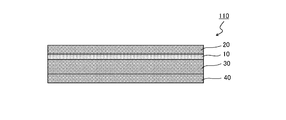
- FIG. 1 is a schematic cross-sectional view of a film for LED backlight according to one embodiment of the present invention.
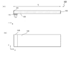
- A is a schematic sectional drawing of the light guide unit by one Embodiment of this invention,
- (b) is a schematic plan view of the light guide unit of (a).
- 1 is a schematic cross-sectional view of an LED backlight according to one embodiment of the present invention.
- FIG. 1 is a schematic cross-sectional view of an LED backlight film according to one embodiment of the present invention.
- the LED backlight film 110 according to this embodiment includes a low refractive index layer 10 and a first pressure-sensitive adhesive layer 20 disposed on at least one side of the low refractive index layer 10.
- the refractive index of the low refractive index layer 10 is 1.25 or less.
- the LED backlight film 110 further includes a substrate 30 as necessary.
- the base material 30 is provided so as to be peelable from the low refractive index layer 10.
- the LED backlight film 110 further includes a second pressure-sensitive adhesive layer 40 as necessary.
- the first pressure-sensitive adhesive layer 20, the low refractive index layer 10, the base material 30, and the second pressure-sensitive adhesive layer 40 are: Arranged in this order.
- each structural member in drawing is modeled, and the size and / or reduced scale are described differently from actual.
- FIG. 2A is a schematic cross-sectional view of a light guide unit according to an embodiment of the present invention
- FIG. 2B is a schematic plan view of the light guide unit of FIG. 2B is a view of the light guide unit 100 of FIG. 2A as viewed from below (the lower side of the drawing).
- the light guide unit 100 includes an LED backlight film 110 and a light guide plate 120.
- the LED backlight film 110 of the present invention can be used by being attached to a part of the main surface of the light guide plate 120.
- the LED backlight film 110 is used by adhering to the vicinity of the light guide direction end face 121 of the light guide plate 120 (the end face 121 where the light source is expected to be arranged).
- the backlight film 110 covers a part of one side of the light guide plate 120 in the light guide direction X, and in a direction Y perpendicular to the light guide direction X in a plane including the light guide direction X.
- the light guide plate 120 may be used by being attached to the light guide plate 120 so as to cover the entire area of one side of the light guide plate 120.
- the LED backlight film 110 may be attached so that the light guide plate 120 and the low refractive index layer 10 are disposed via the first pressure-sensitive adhesive layer 20.
- the LED backlight film 110 is preferably disposed directly on the light guide plate. Further, when the LED backlight film 110 includes the base material 30, the LED backlight film 110 is directly disposed such that the low refractive index layer 10 is on the inner side (light guide plate side) than the base material 30. It is preferable.
- the light guide unit 100 can be applied to a sidelight type planar backlight. For example, the light guide unit 100 can be used by disposing the LED light source 130 on the end surface 121 of the light guide plate 120 and configure the LED backlight 200 together with the LED light source 130 (FIG. 3).
- the light guide direction means a direction perpendicular to an end face on which the light source is planned to be arranged.
- the light guide plate can be fixed to the LED backlight body. Moreover, light can be favorably reflected at the interface between the light guide plate and the LED backlight film, and the light guide efficiency can be improved. By reflecting light well in the vicinity of the incident surface, the emitted light intensity of the entire light guide plate can be increased. Furthermore, if the LED backlight film of the present invention is used as described above, light leakage and brightness unevenness in the vicinity of the incident surface of the light guide plate can be prevented. Furthermore, since the light guide plate can be positioned by adjusting the film thickness of the LED backlight film, the positional relationship between the LED light source and the light guide plate can be easily optimized.
- the thickness of the film for LED backlight is preferably 120 ⁇ m or less, more preferably 110 ⁇ m or less, still more preferably 100 ⁇ m or less, and particularly preferably 60 ⁇ m or less. If it is such a range, when the film for LED backlight is applied to a backlight, the positional relationship of an LED light source and a light-guide plate can be adjusted appropriately.
- the thickness of the LED backlight film may be an appropriate thickness depending on the form of the backlight to which the LED backlight film is applied. The lower limit of the thickness of the LED backlight film is, for example, 10 ⁇ m.
- the heat resistance of the LED backlight film is preferably 60 ° C. or higher, and more preferably 80 ° C. or higher. If it is such a range, the film for LED backlight which can be suitable for the use in the LED light source vicinity and can maintain the said effect favorably can be obtained.
- heat resistance is a change in characteristics before and after charging for 300 hours or longer in an oven at 60 ° C. or 80 ° C. or higher (the amount of emitted light, directivity, and the layer with which the LED backlight film is in direct contact). (Adhesion force) indicates a range that does not affect the use for an LED backlight.
- the refractive index of the low refractive index layer is 1.25 or less. If an LED backlight film having a low refractive index layer having such a refractive index is laminated on a light guide plate, light can be favorably reflected at the interface between the light guide plate and the LED backlight film. An LED backlight having excellent waveguide efficiency and excellent emission intensity can be obtained.
- the refractive index of the low refractive index layer is preferably 1.20 or less, more preferably 1.18 or less, and even more preferably 1.15 or less. The lower the refractive index of the low refractive index layer, the better. However, the lower limit is, for example, 1.07 or more (preferably 1.05 or more). In this specification, the refractive index refers to a refractive index measured at a wavelength of 550 nm.
- the thickness of the low refractive index layer is preferably 0.01 ⁇ m to 100 ⁇ m, more preferably 0.05 ⁇ m to 70 ⁇ m, still more preferably 0.1 ⁇ m to 48 ⁇ m, and particularly preferably 0.3 ⁇ m to 40 ⁇ m. And most preferably from 0.3 ⁇ m to 30 ⁇ m.
- the low refractive index layer may be in any suitable form as long as the refractive index is in the above range.
- the low refractive index layer is configured as a porous body having a predetermined void.
- the porosity of the low refractive index layer configured as a porous body is preferably 5% by volume to 95% by volume, more preferably 15% by volume to 95% by volume, and even more preferably 25% by volume to 90% by volume. More preferably, it is 35 volume% to 90 volume%, particularly preferably 38 volume% to 85 volume%, and most preferably 40 volume% to 80 volume%. Within such a range, a low refractive index layer having a particularly low refractive index can be formed. If the layer whose porosity is to be measured is only a single layer and contains voids, the ratio (volume ratio) between the constituent material of the layer and air can be calculated by a standard method (for example, measuring the weight and volume to calculate the density).
- the porosity (volume%) can be calculated. Further, since there is a correlation between the refractive index and the porosity, for example, the porosity can be calculated from the value of the refractive index of the layer. Specifically, for example, the porosity is calculated from the value of the refractive index measured with an ellipsometer from Lorentz-Lorenz's formula (Lorentz-Lorentz equation).
- the size of the voids is preferably 2 nm to 500 nm, more preferably 5 nm to 500 nm, still more preferably 10 nm to 200 nm, and particularly preferably 20 nm to 100 nm.
- the size of the void can be measured by the BET test method. Specifically, 0.1 g of a low refractive index layer sample was put into a capillary of a specific surface area measuring device (trade name “ASAP2020” manufactured by Micromeritic Co., Ltd.), and then dried under reduced pressure at room temperature for 24 hours. After degassing the gas in the void structure, nitrogen gas is adsorbed on the low refractive index layer sample to obtain a pore distribution, and the void size can be evaluated from the pore distribution.
- a specific surface area measuring device trade name “ASAP2020” manufactured by Micromeritic Co., Ltd.
- the peak pore diameter of the low refractive index layer configured as a porous body is preferably 5 nm to 50 nm, more preferably 10 nm to 40 nm, and still more preferably 20 nm to 30 nm.
- the peak pore diameter is determined from a BJH plot and a BET plot by nitrogen adsorption and an isothermal adsorption line using a pore distribution / specific surface area measuring device (trade name “BELLSORP MINI” manufactured by Microtrack Bell).
- the low refractive index layer configured as a porous body is, for example, silicone particles, silicone particles having fine pores, substantially spherical particles such as silica hollow nanoparticles, fibrous particles such as cellulose nanofibers, alumina nanofibers, silica nanofibers, Including tabular grains such as nanoclay composed of bentonite.
- the low refractive index layer configured as a porous body is a porous body configured by chemically bonding particles to each other.
- at least a part of the particles constituting the low refractive index layer configured as a porous body may be bonded via a small amount of a binder component (for example, a binder component having a particle weight or less).
- the porosity and refractive index of the low refractive index layer configured as a porous body can be adjusted by the particle size, particle size distribution, etc. of the particles constituting the low refractive index layer.
- Examples of a method for obtaining a low refractive index layer configured as a porous body include, for example, JP 2010-189212 A, JP 2008-040171 A, JP 2006-011175 A, and International Publication No. 2004/113966 Pamphlet. And the methods described in those references. Specifically, silica-based compounds; hydrolyzable silanes, a method of hydrolyzing and polycondensing at least one of a partially hydrolyzed product and a dehydrated condensate thereof, porous particles and / or hollow fine particles are used.
- the low refractive index layer is not limited to this manufacturing method, and may be manufactured by any manufacturing method.
- the low refractive index layer is a porous silicone material.
- Silicone porous bodies can be composed of microporous particles of silicon compounds bonded together. Examples of the fine pore particles of the silicon compound include a pulverized product of a gel silicon compound.
- the silicone porous body can be formed, for example, by applying a coating liquid containing a pulverized body of a gel-like silicon compound to a substrate.
- the crushed body of the gel-like silicon compound can be chemically bonded (for example, siloxane bond) by, for example, the action of a catalyst, light irradiation, heating, or the like.
- R 1 is preferably a linear or branched alkyl group having 1 to 6 carbon atoms, more preferably a linear or branched alkyl group having 1 to 4 carbon atoms, and still more preferably a carbon number. 1 or 2 alkyl groups.
- R 2 is preferably a hydrogen atom or a linear or branched alkyl group having 1 to 6 carbon atoms, more preferably a hydrogen atom or a linear or branched alkyl group having 1 to 4 carbon atoms. And more preferably a hydrogen atom or an alkyl group having 1 to 2 carbon atoms.
- silicon compound examples include tris (hydroxy) methylsilane and trimethoxy (methyl) silane.
- the silicon compound is a trifunctional silane. If trifunctional silane is used, a low refractive index layer having a particularly low refractive index can be formed. In another embodiment, the silicon compound is a tetrafunctional silane. If tetrafunctional silane is used, a low refractive index layer having excellent scratch resistance can be formed.
- the gelation of the silicon compound can be performed, for example, by a dehydration condensation reaction of the silicon compound. Any appropriate method can be adopted as the method of the dehydration condensation reaction.
- Arbitrary appropriate methods can be employ
- the pulverization method include a method using a pulverization apparatus using a cavitation phenomenon such as an ultrasonic homogenizer and a high-speed rotation homogenizer.
- the volume average particle diameter of the fine pore particles of the silicon compound is preferably 0.1 ⁇ m to 2 ⁇ m, more preferably 0.2 ⁇ m to 1.5 ⁇ m, and still more preferably 0.2 ⁇ m. 4 ⁇ m to 1 ⁇ m.
- the volume average particle diameter can be measured by a dynamic light scattering method.
- the ratio of the particles having a particle size of 0.4 ⁇ m to 1 ⁇ m to the total amount of the particles is 50% by weight to 99.9% by weight. Preferably, it is 80 to 99.8% by weight, more preferably 90 to 99.7% by weight.
- the ratio of particles having a particle size of 1 ⁇ m to 2 ⁇ m to the total amount of particles is preferably 0.1% by weight to 50% by weight, more preferably 0.2% by weight to 20% by weight, More preferably, it is from 10% by weight to 10% by weight.
- the particle size distribution can be measured by a particle size distribution evaluation apparatus.
- the substrate can be formed of any suitable material.
- suitable material examples include thermoplastic resins such as polyethylene terephthalate resin, acrylic resin, cellulose resin, cycloolefin resin, and olefin resin; thermosetting resins; inorganic materials such as glass and silicon Carbon fiber materials and the like.
- the thickness of the substrate is not particularly limited, and can be set to any appropriate thickness depending on the application.
- the thickness of the substrate is, for example, 1 ⁇ m to 100 ⁇ m, preferably 1 ⁇ m to 60 ⁇ m, and more preferably 2 ⁇ m to 40 ⁇ m.
- the substrate may be transparent or opaque. In one embodiment, the substrate is transparent. When the substrate is transparent, its transmittance is preferably 50% to 99%, more preferably 60% to 99%, and even more preferably 70% to 99%. If it is such a range, even if it is a case where the light omission to a base material arises, the film for LED backlight which can implement
- the 1st adhesive layer contains arbitrary appropriate adhesives.
- the pressure-sensitive adhesive preferably has transparency and optical isotropy.
- Specific examples of the pressure-sensitive adhesive include rubber-based pressure-sensitive adhesives, acrylic pressure-sensitive adhesives, silicone-based pressure-sensitive adhesives, epoxy-based pressure-sensitive adhesives, and cellulose-based pressure-sensitive adhesives.
- it is a rubber adhesive or an acrylic adhesive.
- an acrylic adhesive is used as the adhesive.
- the acrylic pressure-sensitive adhesive include an acrylic pressure-sensitive adhesive having an acrylic polymer (homopolymer or copolymer) containing a structural unit derived from alkyl (meth) acrylate as a base polymer.
- the alkyl group of the alkyl (meth) acrylate has, for example, 2 to 18 carbon atoms.
- the alkyl group may be linear or branched.
- the number of carbon atoms of the alkyl group is preferably 2 to 14, more preferably 3 to 12, and further preferably 4 to 9.
- Specific examples of the alkyl (meth) acrylate include ethyl (meth) acrylate, n-butyl (meth) acrylate, s-butyl (meth) acrylate, t-butyl (meth) acrylate, isobutyl (meth) acrylate, and n-pentyl.
- (Meth) acrylate isopentyl (meth) acrylate, hexyl (meth) acrylate, heptyl (meth) acrylate, isoamyl (meth) acrylate, 2-ethylhexyl (meth) acrylate, n-octyl (meth) acrylate, isooctyl (meth) Acrylate, n-nonyl (meth) acrylate, isononyl (meth) acrylate, n-decyl (meth) acrylate, isodecyl (meth) acrylate, n-dodecyl (meth) acrylate, isomyristyl (meth) acrylate n- tridecyl (meth) acrylate, n- tetradecyl (meth) acrylate, stearyl (meth) acrylate, isostearyl (meth) acrylate.
- the content of the constituent unit derived from alkyl (meth) acrylate is preferably 30 parts by weight to 100 parts by weight, more preferably 85 parts by weight to 99.99 parts by weight with respect to 100 parts by weight of the acrylic polymer. More preferably, it is 90 parts by weight to 99.95 parts by weight, and particularly preferably 95 parts by weight to 99 parts by weight. If it is such a range, the adhesive layer which is excellent in adhesiveness can be formed.
- the acrylic polymer further includes a structural unit derived from a functional group-containing monomer.
- a functional group-containing monomer a monomer having any appropriate functional group may be used.
- Specific examples of the functional group-containing monomer include a carboxyl group-containing monomer, a hydroxyl group-containing monomer, an amide group-containing monomer, and an amino group-containing monomer. If these monomers are used, an adhesive layer having excellent heat resistance can be formed.
- a functional group containing monomer may be used independently and may be used in combination of 2 or more type.
- carboxyl group-containing monomer a polymerizable functional group having an unsaturated double bond such as a (meth) acryloyl group or a vinyl group, and a monomer having a carboxyl group can be used.
- the carboxyl group-containing monomer include (meth) acrylic acid, carboxyethyl (meth) acrylate, carboxypentyl (meth) acrylate, itaconic acid, maleic acid, fumaric acid, and crotonic acid. Of these, (meth) acrylic acid is preferable, and acrylic acid is particularly preferable.
- hydroxyl group-containing monomer a polymerizable functional group having an unsaturated double bond such as a (meth) acryloyl group or a vinyl group, and a monomer having a hydroxyl group can be used.
- the hydroxyl group-containing monomer include 2-hydroxyethyl (meth) acrylate, 2-hydroxybutyl (meth) acrylate, 3-hydroxypropyl (meth) acrylate, 4-hydroxybutyl (meth) acrylate, 6-hydroxyhexyl ( Hydroxyalkyl (meth) acrylates such as (meth) acrylate, 8-hydroxyoctyl (meth) acrylate, 10-hydroxydecyl (meth) acrylate, 12-hydroxylauryl (meth) acrylate; hydroxyethyl (meth) acrylamide, N-methylol ( (Meth) acrylamide, others, (4-hydroxymethylcyclohexyl) methyl acrylate, N-methylol (meth)
- amide group-containing monomer a polymerizable functional group having an unsaturated double bond such as a (meth) acryloyl group or a vinyl group, and a monomer having an amide bond can be used.
- amide group-containing monomers include (meth) acrylamide, N, N-dimethyl (meth) acrylamide, N, N-diethyl (meth) acrylamide, N, N-diethylmethacrylamide, N-isopropyl (meth) acrylamide, N-substituted amide monomers such as N-methoxymethyl (meth) acrylamide, N-butoxymethyl (meth) acrylamide N-vinylcaprolactam, N-acryloylmorpholine, N-acryloylpiperidine, N-methacryloylpiperidine, N-acryloylpyrrolidine, Examples include diacetone (meth) acrylamide and N-vinylacetamide.
- amino group-containing monomer a monomer having a (meth) acryloyl group and an amino group can be used.
- amino group-containing monomer a monomer having a tertiary amino group is preferable.
- the tertiary amino group is preferably a tertiary aminoalkyl group.
- examples of the tertiary amino group-containing monomer include N, N-dialkylaminoalkyl (meth) acrylamide and N, N-dialkylaminoalkyl (meth) acrylate.
- tertiary amino group-containing monomer examples include N, N-dimethylaminoethyl (meth) acrylamide, N, N-dimethylaminopropyl (meth) acrylamide, N, N-diethylaminoethyl (meth) acrylamide, N, N-diethylaminopropyl (meth) acrylamide, N, N-dimethylaminoethyl (meth) acrylate, N, N-dimethylaminopropyl (meth) acrylate, N, N-diethylaminoethyl (meth) acrylate, N, N- Examples include diethylaminopropyl (meth) acrylamide.
- Examples of the monomer having a secondary amino group examples include t-butylaminoethyl (meth) acrylate.
- the content of the structural unit derived from the functional group-containing monomer is preferably 0.01 to 15 parts by weight, more preferably 0.05 to 10 parts by weight with respect to 100 parts by weight of the (meth) acrylic polymer. Parts by weight.
- the acrylic polymer may have a structural unit derived from any appropriate other monomer as necessary.
- Other monomers include phenoxyethyl (meth) acrylate, benzyl (meth) acrylate, phenol ethylene oxide modified (meth) acrylate, 2-naphthoethyl (meth) acrylate, 2- (4-methoxy-1-naphthoxy) ethyl (meth) )
- Aromatic ring-containing monomers such as acrylate, phenoxypropyl (meth) acrylate, phenoxydiethylene glycol (meth) acrylate, polystyryl (meth) acrylate, styrene; vinyl ester monomers such as vinyl acetate and vinyl propionate;
- (meth) acrylic acid examples include (meth) acrylic acid alkoxyalkyl monomers such as methoxyethyl and ethoxyethyl (meth) acrylate. The content ratio of the structural units
- the weight average of the acrylic polymer is preferably 1 million to 3 million, more preferably 1.5 to 2.5 million, and further preferably 1.7 to 2.5 million. If it is such a range, the adhesive layer which is excellent in heat resistance and adhesive force can be obtained.
- the weight average molecular weight is a value measured by GPC (gel permeation chromatography) and calculated in terms of polystyrene.
- the pressure-sensitive adhesive may further contain any appropriate additive as required.
- additives include cross-linking agents, pigments, dyes, surfactants, plasticizers, tackifiers, surface lubricants, leveling agents, softeners, antioxidants, anti-aging agents, light stabilizers, and UV absorbers.
- the crosslinking agent include an isocyanate crosslinking agent, an epoxy crosslinking agent, a peroxide crosslinking agent, a metal chelate crosslinking agent, and an oxazoline crosslinking agent. Of these, an isocyanate-based crosslinking agent is preferable.
- the content of the crosslinking agent is preferably 2 parts by weight or less, more preferably 1.5 parts by weight or less, and further preferably 1 part by weight or less with respect to 100 parts by weight of the acrylic polymer.
- the thickness of the first pressure-sensitive adhesive layer is preferably 0.1 ⁇ m to 100 ⁇ m, more preferably 5 ⁇ m to 50 ⁇ m, and further preferably 5 ⁇ m to 25 ⁇ m.
- the refractive index of the first pressure-sensitive adhesive layer is 1.42 to 1.60, more preferably 1.47 to 1.58. If it is such a range, the LED backlight which is excellent in the waveguide efficiency and excellent in the emission intensity can be obtained.
- the light transmittance of the first pressure-sensitive adhesive layer is preferably 85% to 99%, more preferably 88% to 99%, and further preferably 90% to 99%. Further, the haze value of the first pressure-sensitive adhesive layer is preferably 5 or less, more preferably 3 or less, and further preferably 1 or less.
- the first pressure-sensitive adhesive layer is preferably adhered to the light guide plate side in the light guide unit and the LED backlight. In one embodiment, it adheres directly to the light guide plate or indirectly through a resin layer laminated directly on the light guide plate.
- the adhesive force of the first pressure-sensitive adhesive layer with respect to the layer adjacent to the side opposite to the low refractive index layer of the first pressure-sensitive adhesive layer is preferably 0.8 N / 25 mm or more. More preferably, it is 1 N / 25mm or more, More preferably, it is 1.5 N / 25mm or more. The upper limit of the adhesive force is, for example, 30 N / 25 mm.
- the adhesive strength was measured by a method according to JIS Z 0237: 2000 (bonding condition: 2 kg roller 1 reciprocation, peeling speed: 300 mm / min, peeling angle 180 °) in an environment of 23 ° C. Refers to adhesive strength.
- the 2nd adhesive layer contains arbitrary appropriate adhesives.
- the pressure-sensitive adhesive preferably has transparency and optical isotropy.
- Specific examples of the pressure-sensitive adhesive include rubber-based pressure-sensitive adhesives, acrylic pressure-sensitive adhesives, silicone-based pressure-sensitive adhesives, epoxy-based pressure-sensitive adhesives, and cellulose-based pressure-sensitive adhesives.
- it is a rubber adhesive or an acrylic adhesive.
- the acrylic pressure-sensitive adhesive described in the section A-4 may be used.
- the thickness of the second pressure-sensitive adhesive layer is preferably 0.1 ⁇ m to 100 ⁇ m, more preferably 5 ⁇ m to 50 ⁇ m, and further preferably 5 ⁇ m to 25 ⁇ m.
- the second pressure-sensitive adhesive layer is bonded to a flexible substrate (FPC) in the light guide unit and the LED backlight. In one embodiment, it is in intimate contact with the FPC directly or via a resin layer or insulating layer directly laminated on the FPC.
- the adhesive force of the second pressure-sensitive adhesive layer with respect to the layer adjacent to the side opposite to the low refractive index layer of the second pressure-sensitive adhesive layer is preferably 0.5 N / 25 mm or more. More preferably, it is 0.7 N / 25mm or more, More preferably, it is 1.0 N / 25mm or more. The upper limit of the adhesive force is, for example, 30 N / 25 mm.
- the second pressure-sensitive adhesive layer may be transparent or opaque. In one embodiment, the second pressure-sensitive adhesive layer is transparent.
- the transmittance is preferably 50% to 99%, more preferably 60% to 99%, and further preferably 70% to 99%. If it is such a range, even if it is a case where light leakage arises exceeding a low refractive index layer, the film for LED backlight which can implement
- the LED backlight film can be manufactured by any appropriate method. For example, by applying a coating solution for forming a low refractive index layer containing predetermined particles (for example, fine pore particles of the above-mentioned silicon compound, preferably a pulverized body of a gel-like silicon compound) on the base material, and drying it.
- a coating solution for forming a low refractive index layer containing predetermined particles for example, fine pore particles of the above-mentioned silicon compound, preferably a pulverized body of a gel-like silicon compound
- the low refractive index layer forming coating solution contains any appropriate solvent.
- the solvent include isopropyl alcohol, ethanol, methanol, n-butanol, 2-butanol, isobutyl alcohol, pentanol and the like.
- the low refractive index layer forming coating solution further contains a catalyst.
- a catalyst capable of promoting chemical bonding of particles is used.
- the catalyst include base catalysts such as potassium hydroxide, sodium hydroxide and ammonium hydroxide, and acid catalysts such as hydrochloric acid, acetic acid and oxalic acid. Of these, a base catalyst is preferable.
- the content of the catalyst is preferably 0.01 parts by weight to 20 parts by weight, more preferably 0.1 parts by weight to 5 parts by weight with respect to 100 parts by weight of the particles in the coating solution for forming a low refractive index layer. Part.
- any appropriate method can be adopted as a method for applying the coating liquid for forming a low refractive index layer.
- the coating method include bar coater coating, air knife coating, gravure coating, gravure reverse coating, reverse roll coating, lip coating, die coating, and dip coating.
- drying method of the coating liquid for forming the low refractive index layer Any appropriate method can be adopted as a drying method of the coating liquid for forming the low refractive index layer.
- the drying method of the coating liquid may be natural drying, heat drying, or vacuum drying.
- a heating means a hot air fan, a heating roll, a far-infrared heater, etc. are mentioned, for example.
- the coating layer may be subjected to heat treatment.
- heat treatment bonding between particles constituting the low refractive index layer can be promoted.
- the heating temperature is preferably 200 ° C. or higher.
- the said drying process may serve as heat processing.
- the first pressure-sensitive adhesive layer and the second pressure-sensitive adhesive layer can be formed by any appropriate method.
- the first pressure-sensitive adhesive layer and the second pressure-sensitive adhesive are applied by applying a pressure-sensitive adhesive by a method such as bar coater coating, air knife coating, gravure coating, gravure reverse coating, reverse roll coating, lip coating, die coating, or dip coating.
- An agent layer can be formed.
- the first pressure-sensitive adhesive layer and the second pressure-sensitive adhesive layer may be formed by a method of transferring the pressure-sensitive adhesive layer formed on the release liner.
- the irradiation amount of the electron beam is preferably 2 kGy to 100 kGy, more preferably 2 kGy to 70 kGy, and further preferably 5 to 50 kGy.
- the light guide unit of the present invention includes an LED backlight film 110 and a light guide plate 120 as shown in FIGS. 2 (a) and 2 (b).
- the LED backlight film 110 is laminated and disposed on a part of one side of the light guide plate 120. More specifically, the LED backlight film 110 is adhered and disposed in the vicinity of the light guide direction end surface 121 of the light guide plate 120 (the end surface 121 where the light source is planned to be disposed).
- the backlight film 110 covers a part of one surface 122 of the light guide plate 120 in the light guide direction X of the light guide plate 120 and is perpendicular to the light guide direction X in a plane including the light guide direction X.
- the light guide plate 120 can be attached to the light guide plate 120 so as to cover the entire area of one side 122 of the light guide plate 120.
- the LED backlight film 110 can be attached so that the light guide plate and the low refractive index layer are disposed via the first pressure-sensitive adhesive layer.
- the LED backlight film 110 is preferably disposed directly on the light guide plate.
- the LED backlight film 110 includes a base material, the LED backlight film 110 is preferably arranged directly such that the low refractive index layer is on the inner side (light guide plate side) than the base material. .
- directly disposed means that the LED backlight film 110 and the light guide plate 120 are disposed such that no other layer is disposed between the LED backlight film 110 and the light guide plate 120. Means.
- the surface of the light guide plate to which the LED backlight film is attached corresponds to the surface opposite to the light exit surface when the light guide unit is applied to the LED backlight.
- the LED backlight film may be disposed such that one end thereof is in contact with the end surface of the light guide plate, or may be disposed at a slight distance from the end surface of the light guide plate.
- the distance of the LED backlight film from the light guide plate is preferably 5 mm or less, more preferably 3 mm or less, particularly Preferably it is 1 mm or less.
- the length Lx in the light guide direction of the LED backlight film is preferably 10 mm or less, more preferably 8 mm or less, still more preferably 5 mm or less, and particularly preferably 3 mm or less.
- the lower limit of the length Lx is, for example, 0.5 mm.
- the ratio (Lx / L) of the length Lx in the light guide direction of the LED backlight film to the length L in the light guide direction of the light guide plate is preferably 1/3000 to 1/10, more preferably 1/1000 to 1/20.
- the light intensity of the entire light guide plate can be increased by reflecting light well in the vicinity of the incident surface.
- the LED backlight film can be applied to a region where light is not emitted from the light guide plate.
- the extremely narrow size LED backlight film it is possible to increase the emitted light intensity of the entire light guide plate, and to improve the waveguide efficiency by the member applied to the region where the light emission is not performed. This is the result of the present invention.
- any appropriate material can be used as long as it can efficiently guide the light emitted from the LED light source.
- the material constituting the light guide plate include acrylic resins, polycarbonate resins, and cycloolefin resins.
- the thickness of the light guide plate is, for example, 100 ⁇ m to 2000 ⁇ m.
- the refractive index of the light guide plate is preferably 1.4 or more, more preferably greater than 1.45, even more preferably greater than 1.45 and 2 or less, and particularly preferably 1.48 to 1.8. .
- the difference between the refractive index of the light guide plate and the refractive index layer of the low refractive index layer is preferably 0.2 or more, more preferably 0.23 or more, and further preferably 0.25 or more. Within such a range, light can be favorably reflected at the interface between the light guide plate and the LED backlight film, and an LED backlight unit having excellent light guiding efficiency and excellent emission intensity can be obtained. it can.
- the refractive index of the light guide plate is higher than the refractive index of the low refractive index layer.
- FIG. 3 is a schematic cross-sectional view of an LED backlight according to one embodiment of the present invention.
- the LED backlight 200 may include the light source unit 100 and the LED light source 130 disposed on the end surface 121 on the side where the LED backlight film 110 of the light guide plate 120 included in the light guide unit 100 is disposed.
- the thickness of the LED backlight film is preferably (LED light source thickness-light guide plate thickness) or less. More specifically, the thickness of the film for the LED backlight is ⁇ (LED light source thickness ⁇ light guide plate thickness) ⁇ 10% ⁇ to ⁇ (LED light source thickness ⁇ light guide plate thickness) ⁇ 100% ⁇ . It is more preferable that ⁇ (LED light source thickness ⁇ light guide plate thickness) ⁇ 30% ⁇ to ⁇ (LED light source thickness ⁇ light guide plate thickness) ⁇ 100% ⁇ , ⁇ (LED light source thickness ⁇ The thickness of the light guide plate) ⁇ 50% ⁇ to ⁇ (LED light source thickness ⁇ light guide plate thickness) ⁇ 100% ⁇ is more preferable. If it is such a range, in a backlight unit provided with an LED light source, the positional relationship of an LED light source and a light-guide plate can be adjusted appropriately.
- the thickness of the LED light source is usually 200 ⁇ m to 5000 ⁇ m.
- the LED backlight may further include any appropriate other member.
- the LED backlight 200 may further include a reflecting plate 140 provided via an air layer on the surface of the light guide plate 120 where the LED backlight film 110 is not disposed.
- the flexible substrate 150 for LED may be arrange
- the LED flexible substrate may be provided with a colored layer (for example, a white ink layer) on the surface of the LED backlight film side.
- the LED backlight 200 may include a housing 160 that houses the above-described members.
- ⁇ Evaluation method> (1) Refractive index The refractive index layer was cut into a size of 50 mm x 50 mm, and this was bonded to the surface of a glass plate (thickness: 3 mm) via an adhesive layer. The center of the back surface of the glass plate (diameter of about 20 mm) was painted with black magic to make a sample that did not reflect on the back surface of the glass plate. The above sample was set in an ellipsometer (JA Woollam Japan: VASE), and the refractive index was measured under the conditions of a wavelength of 500 nm and an incident angle of 50 to 80 degrees.
- the LED backlight films obtained in Examples and Comparative Examples are used as LED backlights (light guide plate refractive index: 1.49, LED light source thickness: 300 ⁇ m).
- the brightness unevenness of the light guide plate exit surface when the LED light source was turned on was confirmed visually.
- the case where it was able to illuminate uniformly was set to pass (in Table 1, ⁇ ), and the case where brightness unevenness and light leakage could be confirmed was set to fail (in Table 1, x).
- the gelled silicon compound in the mixed solution D was pulverized (high-pressure medialess pulverization).
- a homogenizer (trade name “UH-50” manufactured by SMT Co., Ltd.) is used, and 1.85 g of gel compound and IBA in the mixed solution D ′ are added to a 5 cc screw bottle. After weighing 15 g, grinding was performed for 2 minutes under conditions of 50 W and 20 kHz.
- the gel silicon compound in the mixed solution D was pulverized, so that the mixed solution D ′ became a sol solution of a pulverized product.
- the volume average particle size indicating the particle size variation of the pulverized product contained in the mixed solution D ′ was confirmed with a dynamic light scattering nanotrack particle size analyzer (manufactured by Nikkiso Co., Ltd., UPA-EX150 type), 0.50 to It was 0.70.
- the acrylic pressure-sensitive adhesive solution is applied to one side of a silicone-treated polyethylene terephthalate (PET) film (Mitsubishi Chemical Polyester Film Co., Ltd., thickness: 38 ⁇ m), and the thickness of the pressure-sensitive adhesive layer after drying is 10 ⁇ m. Then, it was dried at 150 ° C. for 3 minutes to form a first pressure-sensitive adhesive layer.
- PET polyethylene terephthalate
- an isocyanate cross-linking agent coronate L manufactured by Nippon Polyurethane Industry Co., Ltd., adduct of tolylene diisocyanate of trimethylolpropane
- benzoyl peroxide Japan
- An acrylic pressure-sensitive adhesive solution was prepared by blending 0.2 parts of Nyper BMT manufactured by Yushi Co., Ltd. and 0.2 part of ⁇ -glycidoxypropylmethoxysilane (manufactured by Shin-Etsu Chemical Co., Ltd .: KBM-403).
- the acrylic pressure-sensitive adhesive solution is applied on one side of a silicone-treated polyethylene terephthalate (PET) film (Mitsubishi Chemical Polyester Film Co., Ltd., thickness: 38 ⁇ m), and the pressure-sensitive adhesive layer after drying has a thickness of 15 ⁇ m. And then dried at 150 ° C. for 3 minutes to form a second pressure-sensitive adhesive layer.
- PET polyethylene terephthalate
- Example 1 The low refractive index layer coating solution prepared in Production Example 1 is applied to an acrylic resin film (thickness: 20 ⁇ m) as a substrate, dried, and a low refractive index layer (850 nm thick on one side of the substrate ( A laminate having a refractive index of 1.18) was obtained. After irradiating UV (300 mJ) to the low refractive index layer, the pressure-sensitive adhesive layer (first pressure-sensitive adhesive layer) of Production Example 2 is placed on the low refractive index layer side, and the pressure-sensitive adhesive layer of Production Example 3 (second pressure-sensitive adhesive) Layer) to each substrate side and aged at 60 ° C.
- an LED backlight capable of efficiently guiding incident light can be obtained by using the film for LED backlight of the present invention.
Abstract
Provided is an LED backlight film capable of improving waveguide efficiency of a light guide plate in a sidelight-type planar backlight. This LED backlight film comprises a low-refractive index layer, and a first pressure-sensitive adhesive layer disposed on at least one side of the low-refractive index layer, with the refractive index of the low-refractive index layer being 1.25 or less. In one embodiment, the low-refractive index layer is configured as a porous body having a void therein. In one embodiment, the porosity of the low-refractive index layer is 35% by volume or less.
Description
本発明は、LEDバックライト用フィルム、および、これを用いたLEDバックライトに関する。
The present invention relates to a film for LED backlight and an LED backlight using the same.
携帯端末、パーソナルコンピュータ、カーナビゲーション、テレビ等には、画像表示のための液晶表示ディスプレイが広く採用されている。液晶表示ディスプレイには、液晶表示パネルの裏面側に配置され、面状に発光する面状バックライトが多用されている。
Liquid crystal displays for image display are widely used in mobile terminals, personal computers, car navigation systems, televisions and the like. In the liquid crystal display, a planar backlight that is disposed on the back side of the liquid crystal display panel and emits light in a planar shape is often used.
面状バックライトでは、導光板の側端面(以下、入射面という)に光源を配置し、入射面から入射した光を主面(以下、出射面とという)から出射させるサイドライト方式が採用されることが多い。このような面状ライトユニットでは、導光板における導波効率、出射面における明るさの均一性等の向上が一般的な課題となっている。
A planar backlight employs a sidelight system in which a light source is disposed on a side end surface (hereinafter referred to as an incident surface) of a light guide plate and light incident from the incident surface is emitted from a main surface (hereinafter referred to as an output surface). Often. In such a planar light unit, improvement of the waveguide efficiency in the light guide plate, the uniformity of brightness on the exit surface, and the like are common issues.
本発明の課題は、サイドライト方式の面状バックライトにおける導光板の導波効率および明るさの均一性を高め得るLEDバックライト用フィルムを提供することにある。
An object of the present invention is to provide a film for an LED backlight capable of improving the waveguide efficiency and brightness uniformity of a light guide plate in a sidelight type planar backlight.
本発明のLEDバックライト用フィルムは、低屈折率層と、該低屈折率層の少なくとも片側に配置された第1の粘着剤層とを備え、該低屈折率層の屈折率が、1.25以下である。
1つの実施形態においては、上記低屈折率層が空隙を有する多孔体として構成される。
1つの実施形態においては、上記低屈折率層の空隙率が、35体積%以下である。
1つの実施形態においては、上記LEDバックライト用フィルムの厚みが、100μm以下である。
本発明の別の局面によれば導光ユニットが提供される。この導光ユニットは、上記LEDバックライト用フィルムと、導光板とを備え、該LEDバックライト用フィルムが、該導光板の導光方向においては該導光板の片面の一部を覆うようにし、導光方向と垂直な方向においては、該導光板の該片面の全域を覆うようにして、該導光板に貼着されている。
本発明のさらに別の局面によれば、LEDバックライトが提供される。このLEDバックライトは、上記導光ユニットと、上記導光板の前記LEDバックライト用フィルムが配置された側の端面に配置されたLED光源とを備える。
1つの実施形態においては、上記LEDバックライト用フィルムの厚みが、{(LED光源の厚み-導光板の厚み)×50%}~{(LED光源の厚み-導光板の厚み)×100%}である。 The LED backlight film of the present invention comprises a low refractive index layer and a first pressure-sensitive adhesive layer disposed on at least one side of the low refractive index layer, and the refractive index of the low refractive index layer is 1. 25 or less.
In one embodiment, the low refractive index layer is configured as a porous body having voids.
In one embodiment, the porosity of the low refractive index layer is 35% by volume or less.
In one embodiment, the thickness of the film for LED backlight is 100 μm or less.
According to another aspect of the present invention, a light guide unit is provided. The light guide unit includes the LED backlight film and a light guide plate, and the LED backlight film covers a part of one side of the light guide plate in the light guide direction of the light guide plate. In the direction perpendicular to the light guide direction, the light guide plate is attached to the light guide plate so as to cover the entire area of the one side of the light guide plate.
According to yet another aspect of the present invention, an LED backlight is provided. The LED backlight includes the light guide unit and an LED light source disposed on an end surface of the light guide plate on the side where the LED backlight film is disposed.
In one embodiment, the thickness of the LED backlight film is {(LED light source thickness−light guide plate thickness) × 50%} to {(LED light source thickness−light guide plate thickness) × 100%}. It is.
本発明のLEDバックライト用フィルムは、屈折率が1.25以下の低屈折率層を備える。このLEDバックライト用フィルムを用いれば、サイドライト方式の面状バックライトにおける導光板の導波効率および明るさの均一性を高めることができる。
The LED backlight film of the present invention includes a low refractive index layer having a refractive index of 1.25 or less. By using this LED backlight film, it is possible to improve the waveguide efficiency and brightness uniformity of the light guide plate in the sidelight type planar backlight.
A.LEDバックライト用フィルム
A-1.LEDバックライト用フィルムの概要
図1は、本発明の1つの実施形態によるLEDバックライト用フィルムの概略断面図である。この実施形態によるLEDバックライト用フィルム110は、低屈折率層10と、低屈折率層10の少なくとも片側に配置された第1の粘着剤層20とを備える。低屈折率層10の屈折率は、1.25以下である。LEDバックライト用フィルム110は、必要に応じて、基材30をさらに備える。1つの実施形態においては、基材30が備えられる場合、第1の粘着剤層20と、低屈折率層10と、基材30とは、この順に配置される。1つの実施形態においては、基材30は、低屈折率層10から剥離可能に設けられる。LEDバックライト用フィルム110は、必要に応じて、第2の粘着剤層40をさらに備える。1つの実施形態においては、第2の粘着剤層40が備えられる場合、第1の粘着剤層20と、低屈折率層10と、基材30と、第2の粘着剤層40とは、この順に配置される。なお、本明細書においては、見やすくするために、図面における各構成部材は模式化されており、サイズおよび/または縮尺が実際とは異なって記載されている。 A. LED backlight film
A-1. Overview of LED Backlight Film FIG. 1 is a schematic cross-sectional view of an LED backlight film according to one embodiment of the present invention. TheLED backlight film 110 according to this embodiment includes a low refractive index layer 10 and a first pressure-sensitive adhesive layer 20 disposed on at least one side of the low refractive index layer 10. The refractive index of the low refractive index layer 10 is 1.25 or less. The LED backlight film 110 further includes a substrate 30 as necessary. In one embodiment, when the base material 30 is provided, the 1st adhesive layer 20, the low-refractive-index layer 10, and the base material 30 are arrange | positioned in this order. In one embodiment, the base material 30 is provided so as to be peelable from the low refractive index layer 10. The LED backlight film 110 further includes a second pressure-sensitive adhesive layer 40 as necessary. In one embodiment, when the second pressure-sensitive adhesive layer 40 is provided, the first pressure-sensitive adhesive layer 20, the low refractive index layer 10, the base material 30, and the second pressure-sensitive adhesive layer 40 are: Arranged in this order. In addition, in this specification, in order to make it easy to see, each structural member in drawing is modeled, and the size and / or reduced scale are described differently from actual.
A-1.LEDバックライト用フィルムの概要
図1は、本発明の1つの実施形態によるLEDバックライト用フィルムの概略断面図である。この実施形態によるLEDバックライト用フィルム110は、低屈折率層10と、低屈折率層10の少なくとも片側に配置された第1の粘着剤層20とを備える。低屈折率層10の屈折率は、1.25以下である。LEDバックライト用フィルム110は、必要に応じて、基材30をさらに備える。1つの実施形態においては、基材30が備えられる場合、第1の粘着剤層20と、低屈折率層10と、基材30とは、この順に配置される。1つの実施形態においては、基材30は、低屈折率層10から剥離可能に設けられる。LEDバックライト用フィルム110は、必要に応じて、第2の粘着剤層40をさらに備える。1つの実施形態においては、第2の粘着剤層40が備えられる場合、第1の粘着剤層20と、低屈折率層10と、基材30と、第2の粘着剤層40とは、この順に配置される。なお、本明細書においては、見やすくするために、図面における各構成部材は模式化されており、サイズおよび/または縮尺が実際とは異なって記載されている。 A. LED backlight film
A-1. Overview of LED Backlight Film FIG. 1 is a schematic cross-sectional view of an LED backlight film according to one embodiment of the present invention. The
LEDバックライト用フィルムは、導光板に使用され、導光板ともに導光ユニットを構成する。図2(a)は、本発明の1つの実施形態による導光ユニットの概略断面図であり、図2(b)は、図2(a)の導光ユニットの概略平面図である。なお、図2(b)は、図2(a)の導光ユニット100を下方(紙面下側)から見た図である。導光ユニット100は、LEDバックライト用フィルム110と導光板120とを備える。本発明のLEDバックライト用フィルム110は、導光板120の主面の一部に貼着して使用され得る。より詳細には、LEDバックライト用フィルム110は、導光板120の導光方向端面121(光源の配置が予定される端面121)の近傍に、貼着して用いられる。好ましくは、バックライトフィルム用フィルム110は、導光方向Xにおいては導光板120の片面の一部を覆うようにし、導光方向Xを含む面内において導光方向Xと垂直な方向Yにおいては、導光板120の片面の全域を覆うようにして、導光板120に貼着して使用され得る。LEDバックライト用フィルム110は、第1の粘着剤層20を介して、導光板120と低屈折率層10とが配置するようにして貼着され得る。LEDバックライト用フィルム110は、導光板に直接配置されることが好ましい。また、LEDバックライト用フィルム110が基材30を備える場合、LEDバックライト用フィルム110は、低屈折率層10が基材30よりも内側(導光板側)となるようにして直接配置されることが好ましい。導光ユニット100は、サイドライト方式の面状バックライトに適用され得る。例えば、導光ユニット100は、導光板120の端面121にLED光源130を配置して用いられ、LED光源130とともにLEDバックライト200を構成し得る(図3)。なお、本明細書において、導光方向とは、光源の配置が予定される端面に垂直な方向を意味する。
The LED backlight film is used for a light guide plate and constitutes a light guide unit together with the light guide plate. FIG. 2A is a schematic cross-sectional view of a light guide unit according to an embodiment of the present invention, and FIG. 2B is a schematic plan view of the light guide unit of FIG. 2B is a view of the light guide unit 100 of FIG. 2A as viewed from below (the lower side of the drawing). The light guide unit 100 includes an LED backlight film 110 and a light guide plate 120. The LED backlight film 110 of the present invention can be used by being attached to a part of the main surface of the light guide plate 120. More specifically, the LED backlight film 110 is used by adhering to the vicinity of the light guide direction end face 121 of the light guide plate 120 (the end face 121 where the light source is expected to be arranged). Preferably, the backlight film 110 covers a part of one side of the light guide plate 120 in the light guide direction X, and in a direction Y perpendicular to the light guide direction X in a plane including the light guide direction X. The light guide plate 120 may be used by being attached to the light guide plate 120 so as to cover the entire area of one side of the light guide plate 120. The LED backlight film 110 may be attached so that the light guide plate 120 and the low refractive index layer 10 are disposed via the first pressure-sensitive adhesive layer 20. The LED backlight film 110 is preferably disposed directly on the light guide plate. Further, when the LED backlight film 110 includes the base material 30, the LED backlight film 110 is directly disposed such that the low refractive index layer 10 is on the inner side (light guide plate side) than the base material 30. It is preferable. The light guide unit 100 can be applied to a sidelight type planar backlight. For example, the light guide unit 100 can be used by disposing the LED light source 130 on the end surface 121 of the light guide plate 120 and configure the LED backlight 200 together with the LED light source 130 (FIG. 3). In the present specification, the light guide direction means a direction perpendicular to an end face on which the light source is planned to be arranged.
上記のようにして本発明のLEDバックライト用フィルムを用いれば、LEDバックライト本体への導光板の固定が可能となる。また、導光板とLEDバックライト用フィルムとの界面において光を良好に反射させることができ、光の導波効率の向上を図ることができる。入射面近傍において、光を良好に反射させることにより、導光板全体の出射光強度を高めることができる。さらに、上記のようにして本発明のLEDバックライト用フィルムを用いれば、導光板の入射面近傍における光漏れ、明るさのムラを防止することができる。さらに、LEDバックライト用フィルム厚みの調整により、導光板の位置決めをすることが可能となるため、LED光源と導光板との位置関係を容易に適正化することができる。
If the LED backlight film of the present invention is used as described above, the light guide plate can be fixed to the LED backlight body. Moreover, light can be favorably reflected at the interface between the light guide plate and the LED backlight film, and the light guide efficiency can be improved. By reflecting light well in the vicinity of the incident surface, the emitted light intensity of the entire light guide plate can be increased. Furthermore, if the LED backlight film of the present invention is used as described above, light leakage and brightness unevenness in the vicinity of the incident surface of the light guide plate can be prevented. Furthermore, since the light guide plate can be positioned by adjusting the film thickness of the LED backlight film, the positional relationship between the LED light source and the light guide plate can be easily optimized.
LEDバックライト用フィルムの厚みは、好ましくは120μm以下であり、より好ましくは110μm以下であり、さらに好ましくは100μm以下であり、特に好ましくは60μm以下である。このような範囲であれば、LEDバックライト用フィルムをバックライトに適用した際に、LED光源と導光板との位置関係を適切に調整することができる。LEDバックライト用フィルムの厚みは、当該LEDバックライト用フィルムが適用されるバックライトの形態に応じて、適切な厚みとされ得る。LEDバックライト用フィルムの厚みの下限は例えば、10μmである。
The thickness of the film for LED backlight is preferably 120 μm or less, more preferably 110 μm or less, still more preferably 100 μm or less, and particularly preferably 60 μm or less. If it is such a range, when the film for LED backlight is applied to a backlight, the positional relationship of an LED light source and a light-guide plate can be adjusted appropriately. The thickness of the LED backlight film may be an appropriate thickness depending on the form of the backlight to which the LED backlight film is applied. The lower limit of the thickness of the LED backlight film is, for example, 10 μm.
LEDバックライト用フィルムは、耐熱性が、60℃以上であることが好ましく、80℃以上であることがさらに好ましい。このような範囲であれば、LED光源近傍での使用に適し、上記効果が良好に維持され得るLEDバックライト用フィルムを得ることができる。なお、耐熱性とは、60℃もしくは80℃以上のオーブンに300時間以上投入した際の投入前後での特性変化(出射光量、指向性、LEDバックライト用フィルムが直接接触している層との密着力)が、LEDバックライト用の使用に影響ない範囲であることを指す。
The heat resistance of the LED backlight film is preferably 60 ° C. or higher, and more preferably 80 ° C. or higher. If it is such a range, the film for LED backlight which can be suitable for the use in the LED light source vicinity and can maintain the said effect favorably can be obtained. In addition, heat resistance is a change in characteristics before and after charging for 300 hours or longer in an oven at 60 ° C. or 80 ° C. or higher (the amount of emitted light, directivity, and the layer with which the LED backlight film is in direct contact). (Adhesion force) indicates a range that does not affect the use for an LED backlight.
A-2.低屈折率層
上記のとおり、低屈折率層の屈折率は、1.25以下である。このような屈折率を有する低屈折率層を有するLEDバックライト用フィルムを導光板に積層すれば、導光板とLEDバックライト用フィルムとの界面において光を良好に反射させることができ、光の導波効率に優れ、出射強度に優れるLEDバックライトを得ることができる。低屈折率層の屈折率は、好ましくは1.20以下であり、より好ましくは1.18以下であり、さらに好ましくは1.15以下である。低屈折率層の屈折率は低いほど好ましいが、その下限は、例えば、1.07以上(好ましくは1.05以上)である。本明細書において、屈折率とは、波長550nmにおいて測定された屈折率をいう。 A-2. Low Refractive Index Layer As described above, the refractive index of the low refractive index layer is 1.25 or less. If an LED backlight film having a low refractive index layer having such a refractive index is laminated on a light guide plate, light can be favorably reflected at the interface between the light guide plate and the LED backlight film. An LED backlight having excellent waveguide efficiency and excellent emission intensity can be obtained. The refractive index of the low refractive index layer is preferably 1.20 or less, more preferably 1.18 or less, and even more preferably 1.15 or less. The lower the refractive index of the low refractive index layer, the better. However, the lower limit is, for example, 1.07 or more (preferably 1.05 or more). In this specification, the refractive index refers to a refractive index measured at a wavelength of 550 nm.
上記のとおり、低屈折率層の屈折率は、1.25以下である。このような屈折率を有する低屈折率層を有するLEDバックライト用フィルムを導光板に積層すれば、導光板とLEDバックライト用フィルムとの界面において光を良好に反射させることができ、光の導波効率に優れ、出射強度に優れるLEDバックライトを得ることができる。低屈折率層の屈折率は、好ましくは1.20以下であり、より好ましくは1.18以下であり、さらに好ましくは1.15以下である。低屈折率層の屈折率は低いほど好ましいが、その下限は、例えば、1.07以上(好ましくは1.05以上)である。本明細書において、屈折率とは、波長550nmにおいて測定された屈折率をいう。 A-2. Low Refractive Index Layer As described above, the refractive index of the low refractive index layer is 1.25 or less. If an LED backlight film having a low refractive index layer having such a refractive index is laminated on a light guide plate, light can be favorably reflected at the interface between the light guide plate and the LED backlight film. An LED backlight having excellent waveguide efficiency and excellent emission intensity can be obtained. The refractive index of the low refractive index layer is preferably 1.20 or less, more preferably 1.18 or less, and even more preferably 1.15 or less. The lower the refractive index of the low refractive index layer, the better. However, the lower limit is, for example, 1.07 or more (preferably 1.05 or more). In this specification, the refractive index refers to a refractive index measured at a wavelength of 550 nm.
上記低屈折率層の厚みは、好ましくは0.01μm~100μmであり、より好ましくは0.05μm~70μmであり、さらに好ましくは0.1μm~48μmであり、特に好ましくは0.3μm~40μmであり、最も好ましくは0.3μm~30μmである。
The thickness of the low refractive index layer is preferably 0.01 μm to 100 μm, more preferably 0.05 μm to 70 μm, still more preferably 0.1 μm to 48 μm, and particularly preferably 0.3 μm to 40 μm. And most preferably from 0.3 μm to 30 μm.
上記低屈折率層は、屈折率が上記範囲にある限り、任意の適切な形態であり得る。1つの実施形態においては、低屈折率層は、所定の空隙を有する多孔体として構成される。
The low refractive index layer may be in any suitable form as long as the refractive index is in the above range. In one embodiment, the low refractive index layer is configured as a porous body having a predetermined void.
多孔体として構成される低屈折率層の空隙率は、好ましくは5体積%~95体積%であり、より好ましくは15体積%~95体積%であり、さらに好ましくは25体積%~90体積%であり、さらに好ましくは35体積%~90体積%であり、特に好ましくは38体積%~85体積%であり、最も好ましくは40体積%~80体積%である。このような範囲であれば、屈折率が特に低い低屈折率層を形成することができる。空隙率の測定対象となる層が単一層で空隙を含んでいるだけならば、層の構成物質と空気との割合(体積比)は、定法(例えば重量および体積を測定して密度を算出する)により算出することが可能であるため、これにより、空隙率(体積%)を算出できる。また、屈折率と空隙率は相関関係があるため、例えば、層としての屈折率の値から空隙率を算出することもできる。具体的には、例えば、エリプソメーターで測定した屈折率の値から、Lorentz‐Lorenz’s formula(ローレンツ-ローレンツの式)より空隙率を算出する。
The porosity of the low refractive index layer configured as a porous body is preferably 5% by volume to 95% by volume, more preferably 15% by volume to 95% by volume, and even more preferably 25% by volume to 90% by volume. More preferably, it is 35 volume% to 90 volume%, particularly preferably 38 volume% to 85 volume%, and most preferably 40 volume% to 80 volume%. Within such a range, a low refractive index layer having a particularly low refractive index can be formed. If the layer whose porosity is to be measured is only a single layer and contains voids, the ratio (volume ratio) between the constituent material of the layer and air can be calculated by a standard method (for example, measuring the weight and volume to calculate the density). ), The porosity (volume%) can be calculated. Further, since there is a correlation between the refractive index and the porosity, for example, the porosity can be calculated from the value of the refractive index of the layer. Specifically, for example, the porosity is calculated from the value of the refractive index measured with an ellipsometer from Lorentz-Lorenz's formula (Lorentz-Lorentz equation).
上記空隙のサイズは、好ましくは2nm~500nmであり、より好ましくは5nm~500nmであり、さらに好ましくは10nm~200nmであり、特に好ましくは20nm~100nmである。空隙のサイズは、BET試験法により測定することができる。具体的には、比表面積測定装置(マイクロメリティック社製の商品名「ASAP2020」)のキャピラリに、低屈折率層サンプルを0.1g投入した後、室温で24時間、減圧乾燥を行って、空隙構造内の気体を脱気し、その後、低屈折率層サンプルに窒素ガスを吸着させて細孔分布を得、細孔分布から空隙サイズを評価することができる。
The size of the voids is preferably 2 nm to 500 nm, more preferably 5 nm to 500 nm, still more preferably 10 nm to 200 nm, and particularly preferably 20 nm to 100 nm. The size of the void can be measured by the BET test method. Specifically, 0.1 g of a low refractive index layer sample was put into a capillary of a specific surface area measuring device (trade name “ASAP2020” manufactured by Micromeritic Co., Ltd.), and then dried under reduced pressure at room temperature for 24 hours. After degassing the gas in the void structure, nitrogen gas is adsorbed on the low refractive index layer sample to obtain a pore distribution, and the void size can be evaluated from the pore distribution.
多孔体として構成される低屈折率層のピーク細孔径は、好ましくは5nm~50nmであり、より好ましくは10nm~40nmであり、さらに好ましくは20nm~30nmである。ピーク細孔径は、細孔分布/比表面積測定装置(マイクロトラックベル社の商品名「BELLSORP MINI」)を用いて、窒素吸着によるBJHプロットおよびBETプロット、ならびに等温吸着線から求められる。
The peak pore diameter of the low refractive index layer configured as a porous body is preferably 5 nm to 50 nm, more preferably 10 nm to 40 nm, and still more preferably 20 nm to 30 nm. The peak pore diameter is determined from a BJH plot and a BET plot by nitrogen adsorption and an isothermal adsorption line using a pore distribution / specific surface area measuring device (trade name “BELLSORP MINI” manufactured by Microtrack Bell).
多孔体として構成される低屈折率層は、例えば、シリコーン粒子、微細孔を有するシリコーン粒子、シリカ中空ナノ粒子等の略球状粒子、セルロースナノファイバー、アルミナナノファイバー、シリカナノファイバー等の繊維状粒子、ベントナイトから構成されるナノクレイ等の平板状粒子等を含む。1つの実施形態において、多孔体として構成される低屈折率層は、粒子同士が化学的に結合して構成される多孔体である。また、多孔体として構成される低屈折率層を構成する粒子同士は、その少なくとも一部が、少量のバインダー成分(例えば、粒子重量以下のバインダー成分)を介して結合していてもよい。多孔体として構成される低屈折率層の空隙率および屈折率は、当該低屈折率層を構成する粒子の粒径、粒径分布等により調整することができる。
The low refractive index layer configured as a porous body is, for example, silicone particles, silicone particles having fine pores, substantially spherical particles such as silica hollow nanoparticles, fibrous particles such as cellulose nanofibers, alumina nanofibers, silica nanofibers, Including tabular grains such as nanoclay composed of bentonite. In one embodiment, the low refractive index layer configured as a porous body is a porous body configured by chemically bonding particles to each other. In addition, at least a part of the particles constituting the low refractive index layer configured as a porous body may be bonded via a small amount of a binder component (for example, a binder component having a particle weight or less). The porosity and refractive index of the low refractive index layer configured as a porous body can be adjusted by the particle size, particle size distribution, etc. of the particles constituting the low refractive index layer.
多孔体として構成される低屈折率層を得る方法としては、例えば、特開2010-189212号公報、特開2008-040171号公報、特開2006-011175号公報、国際公開第2004/113966号パンフレット、およびそれらの参考文献に記載された方法が挙げられる。具体的には、シリカ系化合物;加水分解性シラン類、ならびにその部分加水分解物および脱水縮合物の少なくともいずれか1つを加水分解及び重縮合させる方法、多孔質粒子および/または中空微粒子を用いる方法、ならびにスプリングバック現象を利用してエアロゲル層を生成する方法、ゾルゲルにより得られたゲルを粉砕し、かつ上記粉砕液中の微細孔粒子同士を触媒等で化学的に結合させた粉砕ゲルを用いる方法、等が挙げられる。ただし、低屈折率層は、この製造方法に限定されず、どのような製造方法により製造しても良い。
Examples of a method for obtaining a low refractive index layer configured as a porous body include, for example, JP 2010-189212 A, JP 2008-040171 A, JP 2006-011175 A, and International Publication No. 2004/113966 Pamphlet. And the methods described in those references. Specifically, silica-based compounds; hydrolyzable silanes, a method of hydrolyzing and polycondensing at least one of a partially hydrolyzed product and a dehydrated condensate thereof, porous particles and / or hollow fine particles are used. And a method of generating an airgel layer using a springback phenomenon, a pulverized gel obtained by pulverizing a gel obtained from a sol gel and chemically bonding fine pore particles in the pulverized liquid with a catalyst or the like. The method used, etc. are mentioned. However, the low refractive index layer is not limited to this manufacturing method, and may be manufactured by any manufacturing method.
好ましくは、上記低屈折率層は、シリコーン多孔体である。シリコーン多孔体は、互いに結合したケイ素化合物の微細孔粒子から構成され得る。ケイ素化合物の微細孔粒子としては、ゲル状ケイ素化合物の粉砕体が挙げられる。シリコーン多孔体は、例えば、ゲル状ケイ素化合物の粉砕体を含む塗工液を、基材に塗工して形成され得る。1つの実施形態においては、ゲル状ケイ素化合物の粉砕体は、例えば、触媒の作用、光照射、加熱等により化学的に結合(例えば、シロキサン結合)し得る。
Preferably, the low refractive index layer is a porous silicone material. Silicone porous bodies can be composed of microporous particles of silicon compounds bonded together. Examples of the fine pore particles of the silicon compound include a pulverized product of a gel silicon compound. The silicone porous body can be formed, for example, by applying a coating liquid containing a pulverized body of a gel-like silicon compound to a substrate. In one embodiment, the crushed body of the gel-like silicon compound can be chemically bonded (for example, siloxane bond) by, for example, the action of a catalyst, light irradiation, heating, or the like.
ケイ素化合物としては、例えば、下記式(1)で表される化合物が挙げられる。

式(1)中、Xは2、3または4である。R1は、好ましくは炭素数1~6の直鎖状または分岐状のアルキル基であり、より好ましくは炭素数1~4の直鎖状または分岐状のアルキル基であり、さらに好ましくは炭素数1~2のアルキル基である。R2は、好ましくは水素原子または炭素数1~6の直鎖状もしくは分岐状のアルキル基であり、より好ましくは水素原子または炭素数1~4の直鎖状または分岐状のアルキル基であり、さらに好ましくは水素原子または炭素数1~2のアルキル基である。
As a silicon compound, the compound represented by following formula (1) is mentioned, for example.
In the formula (1), X is 2, 3 or 4. R 1 is preferably a linear or branched alkyl group having 1 to 6 carbon atoms, more preferably a linear or branched alkyl group having 1 to 4 carbon atoms, and still more preferably a carbon number. 1 or 2 alkyl groups. R 2 is preferably a hydrogen atom or a linear or branched alkyl group having 1 to 6 carbon atoms, more preferably a hydrogen atom or a linear or branched alkyl group having 1 to 4 carbon atoms. And more preferably a hydrogen atom or an alkyl group having 1 to 2 carbon atoms.
上記ケイ素化合物の具体例としては、例えば、トリス(ヒドロキシ)メチルシラン、トリメトキシ(メチル)シラン等が挙げられる。
Specific examples of the silicon compound include tris (hydroxy) methylsilane and trimethoxy (methyl) silane.
1つの実施形態においては、ケイ素化合物は3官能シランである。3官能シランを用いれば、屈折率が特に低い低屈折率層を形成することができる。別の実施形態においては、ケイ素化合物は4官能シランである。4官能シランを用いれば、耐擦傷性に優れる低屈折率層を形成することができる。
In one embodiment, the silicon compound is a trifunctional silane. If trifunctional silane is used, a low refractive index layer having a particularly low refractive index can be formed. In another embodiment, the silicon compound is a tetrafunctional silane. If tetrafunctional silane is used, a low refractive index layer having excellent scratch resistance can be formed.
ケイ素化合物のゲル化は、例えば、ケイ素化合物の脱水縮合反応により行われ得る。脱水縮合反応の方法は、任意の適切な方法が採用され得る。
The gelation of the silicon compound can be performed, for example, by a dehydration condensation reaction of the silicon compound. Any appropriate method can be adopted as the method of the dehydration condensation reaction.
ゲル状ケイ素化合物の粉砕方法としては、任意の適切な方法が採用され得る。粉砕方法としては、例えば、超音波ホモジナイザー、高速回転ホモジナイザー等のキャビテーション現象を用いる粉砕装置を用いる方法が挙げられる。
Arbitrary appropriate methods can be employ | adopted as a grinding method of a gel-like silicon compound. Examples of the pulverization method include a method using a pulverization apparatus using a cavitation phenomenon such as an ultrasonic homogenizer and a high-speed rotation homogenizer.
ケイ素化合物の微細孔粒子(ゲル状ケイ素化合物の粉砕体)の体積平均粒子径は、好ましくは0.1μm~2μmであり、より好ましくは0.2μm~1.5μmであり、さらに好ましくは0.4μm~1μmである。体積平均粒子径は、動的光散乱法により測定され得る。
The volume average particle diameter of the fine pore particles of the silicon compound (the pulverized product of the gel-like silicon compound) is preferably 0.1 μm to 2 μm, more preferably 0.2 μm to 1.5 μm, and still more preferably 0.2 μm. 4 μm to 1 μm. The volume average particle diameter can be measured by a dynamic light scattering method.
ケイ素化合物の微細孔粒子(ゲル状ケイ素化合物の粉砕体)の粒度分布としては、粒径0.4μm~1μmの粒子の粒子全量に対する割合が、50重量%~99.9重量%であることが好ましく、80重量%~99.8重量%であることがより好ましく、90重量%~99.7重量%であることがさらに好ましい。また、粒子径1μm~2μmの粒子の粒子全量に対する割合が、0.1重量%~50重量%であることが好ましく、0.2重量%~20重量%であることがより好ましく、0.3重量%~10重量%であることがさらに好ましい。粒度分布は、粒度分布評価装置により測定することができる。
As the particle size distribution of the fine pore particles of the silicon compound (the crushed product of the gel-like silicon compound), the ratio of the particles having a particle size of 0.4 μm to 1 μm to the total amount of the particles is 50% by weight to 99.9% by weight. Preferably, it is 80 to 99.8% by weight, more preferably 90 to 99.7% by weight. The ratio of particles having a particle size of 1 μm to 2 μm to the total amount of particles is preferably 0.1% by weight to 50% by weight, more preferably 0.2% by weight to 20% by weight, More preferably, it is from 10% by weight to 10% by weight. The particle size distribution can be measured by a particle size distribution evaluation apparatus.
A-3.基材
上記基材は、任意の適切な材料で形成され得る。基材を構成する材料としては、例えば、ポリエチレンテレフタレート系樹脂、アクリル系樹脂、セルロース系樹脂、シクロオレフィン系樹脂、オレフィン系樹脂等の熱可塑性樹脂;熱硬化性樹脂;ガラス、シリコン等の無機材料;炭素繊維材料等が挙げられる。 A-3. Substrate The substrate can be formed of any suitable material. Examples of the material constituting the substrate include thermoplastic resins such as polyethylene terephthalate resin, acrylic resin, cellulose resin, cycloolefin resin, and olefin resin; thermosetting resins; inorganic materials such as glass and silicon Carbon fiber materials and the like.
上記基材は、任意の適切な材料で形成され得る。基材を構成する材料としては、例えば、ポリエチレンテレフタレート系樹脂、アクリル系樹脂、セルロース系樹脂、シクロオレフィン系樹脂、オレフィン系樹脂等の熱可塑性樹脂;熱硬化性樹脂;ガラス、シリコン等の無機材料;炭素繊維材料等が挙げられる。 A-3. Substrate The substrate can be formed of any suitable material. Examples of the material constituting the substrate include thermoplastic resins such as polyethylene terephthalate resin, acrylic resin, cellulose resin, cycloolefin resin, and olefin resin; thermosetting resins; inorganic materials such as glass and silicon Carbon fiber materials and the like.
上記基材の厚みは特に限定されず、用途に応じて、任意の適切な厚みに設定され得る。基材の厚みは、例えば、1μm~100μmであり、好ましくは1μm~60μmであり、さらに好ましくは2μm~40μmである。
The thickness of the substrate is not particularly limited, and can be set to any appropriate thickness depending on the application. The thickness of the substrate is, for example, 1 μm to 100 μm, preferably 1 μm to 60 μm, and more preferably 2 μm to 40 μm.
基材は透明であってもよく、不透明であってもよい。1つの実施形態においては、基材は透明である。基材が透明である場合、その透過率は、好ましくは50%~99%であり、より好ましくは60%~99%であり、さらに好ましくは70%~99%である。このような範囲であれば、基材への光抜けが生じた場合であっても、適切な導光を実現し得るLEDバックライト用フィルムを得ることができる。
The substrate may be transparent or opaque. In one embodiment, the substrate is transparent. When the substrate is transparent, its transmittance is preferably 50% to 99%, more preferably 60% to 99%, and even more preferably 70% to 99%. If it is such a range, even if it is a case where the light omission to a base material arises, the film for LED backlight which can implement | achieve appropriate light guide can be obtained.
A-4.第1の粘着剤層
第1の粘着剤層は、任意の適切な粘着剤を含む。粘着剤は、好ましくは、透明性および光学的等方性を有する。粘着剤の具体例としては、ゴム系粘着剤、アクリル系粘着剤、シリコーン系粘着剤、エポキシ系粘着剤、セルロース系粘着剤が挙げられる。好ましくは、ゴム系粘着剤またはアクリル系粘着剤である。 A-4. 1st adhesive layer The 1st adhesive layer contains arbitrary appropriate adhesives. The pressure-sensitive adhesive preferably has transparency and optical isotropy. Specific examples of the pressure-sensitive adhesive include rubber-based pressure-sensitive adhesives, acrylic pressure-sensitive adhesives, silicone-based pressure-sensitive adhesives, epoxy-based pressure-sensitive adhesives, and cellulose-based pressure-sensitive adhesives. Preferably, it is a rubber adhesive or an acrylic adhesive.
第1の粘着剤層は、任意の適切な粘着剤を含む。粘着剤は、好ましくは、透明性および光学的等方性を有する。粘着剤の具体例としては、ゴム系粘着剤、アクリル系粘着剤、シリコーン系粘着剤、エポキシ系粘着剤、セルロース系粘着剤が挙げられる。好ましくは、ゴム系粘着剤またはアクリル系粘着剤である。 A-4. 1st adhesive layer The 1st adhesive layer contains arbitrary appropriate adhesives. The pressure-sensitive adhesive preferably has transparency and optical isotropy. Specific examples of the pressure-sensitive adhesive include rubber-based pressure-sensitive adhesives, acrylic pressure-sensitive adhesives, silicone-based pressure-sensitive adhesives, epoxy-based pressure-sensitive adhesives, and cellulose-based pressure-sensitive adhesives. Preferably, it is a rubber adhesive or an acrylic adhesive.
1つの実施形態においては、上記粘着剤として、アクリル系粘着剤が用いられる。アクリル系粘着剤としては、例えば、アルキル(メタ)アクリレート由来の構成単位を含むアクリル系ポリマー(ホモポリマーまたはコポリマー)をベースポリマーとするアクリル系粘着剤等挙げられる。
In one embodiment, an acrylic adhesive is used as the adhesive. Examples of the acrylic pressure-sensitive adhesive include an acrylic pressure-sensitive adhesive having an acrylic polymer (homopolymer or copolymer) containing a structural unit derived from alkyl (meth) acrylate as a base polymer.
アルキル(メタ)アクリレートとしては、アルキル(メタ)アクリレートのアルキル基の炭素数は例えば、2~18である。アルキル基は直鎖、分岐鎖のいずれでもよい。アルキル基の炭素数は、好ましくは2~14であり、より好ましくは3~12であり、さらに好ましくは4~9である。アルキル(メタ)アクリレートの具体例としては、エチル(メタ)アクリレート、n-ブチル(メタ)アクリレート、s-ブチル(メタ)アクリレート、t-ブチル(メタ)アクリレート、イソブチル(メタ)アクリレート、n-ペンチル(メタ)アクリレート、イソペンチル(メタ)アクリレート、へキシル(メタ)アクリレート、ヘプチル(メタ)アクリレート、イソアミル(メタ)アクリレート、2-エチルヘキシル(メタ)アクリレート、n-オクチル(メタ)アクリレート、イソオクチル(メタ)アクリレート、n-ノニル(メタ)アクリレート、イソノニル(メタ)アクリレート、n-デシル(メタ)アクリレート、イソデシル(メタ)アクリレート、n-ドデシル(メタ)アクリレート、イソミリスチル(メタ)アクリレート、n-トリデシル(メタ)アクリレート、n-テトラデシル(メタ)アクリレート、ステアリル(メタ)アクリレート、イソステアリル(メタ)アクリレート等が挙げられる。なかでも好ましくは、n-ブチル(メタ)アクリレート、2-エチルヘキシル(メタ)アクリレートである。これらのモノマーは、単独で用いてもよく、2種以上を組み合わせて用いてもよい。
As the alkyl (meth) acrylate, the alkyl group of the alkyl (meth) acrylate has, for example, 2 to 18 carbon atoms. The alkyl group may be linear or branched. The number of carbon atoms of the alkyl group is preferably 2 to 14, more preferably 3 to 12, and further preferably 4 to 9. Specific examples of the alkyl (meth) acrylate include ethyl (meth) acrylate, n-butyl (meth) acrylate, s-butyl (meth) acrylate, t-butyl (meth) acrylate, isobutyl (meth) acrylate, and n-pentyl. (Meth) acrylate, isopentyl (meth) acrylate, hexyl (meth) acrylate, heptyl (meth) acrylate, isoamyl (meth) acrylate, 2-ethylhexyl (meth) acrylate, n-octyl (meth) acrylate, isooctyl (meth) Acrylate, n-nonyl (meth) acrylate, isononyl (meth) acrylate, n-decyl (meth) acrylate, isodecyl (meth) acrylate, n-dodecyl (meth) acrylate, isomyristyl (meth) acrylate n- tridecyl (meth) acrylate, n- tetradecyl (meth) acrylate, stearyl (meth) acrylate, isostearyl (meth) acrylate. Of these, n-butyl (meth) acrylate and 2-ethylhexyl (meth) acrylate are preferable. These monomers may be used independently and may be used in combination of 2 or more type.
アルキル(メタ)アクリレート由来の構成単位の含有割合は、アクリル系ポリマー100重量部に対して、好ましくは30重量部~100重量部であり、より好ましくは85重量部~99.99重量部であり、さらに好ましくは90重量部~99.95重量部であり、特に好ましくは95重量部~99重量部である。このような範囲であれば、粘着性に優れる粘着剤層を形成することができる。
The content of the constituent unit derived from alkyl (meth) acrylate is preferably 30 parts by weight to 100 parts by weight, more preferably 85 parts by weight to 99.99 parts by weight with respect to 100 parts by weight of the acrylic polymer. More preferably, it is 90 parts by weight to 99.95 parts by weight, and particularly preferably 95 parts by weight to 99 parts by weight. If it is such a range, the adhesive layer which is excellent in adhesiveness can be formed.
1つの実施形態においては、上記アクリル系ポリマーは、官能基含有モノマー由来の構成単位をさらに有する。官能基含有モノマーとしては、任意の適切な官能基を有するモノマーが用いられ得る。官能基含有モノマーの具体例としては、例えば、カルボキシル基含有モノマー、ヒドロキシル基含有モノマー、アミド基含有モノマー、アミノ基含有モノマー等が挙げられる。これらのモノマーを用いれば、耐熱性に優れる粘着剤層を形成することができる。官能基含有モノマーは、単独で用いてもよく、2種以上を組み合わせて用いてもよい。
In one embodiment, the acrylic polymer further includes a structural unit derived from a functional group-containing monomer. As the functional group-containing monomer, a monomer having any appropriate functional group may be used. Specific examples of the functional group-containing monomer include a carboxyl group-containing monomer, a hydroxyl group-containing monomer, an amide group-containing monomer, and an amino group-containing monomer. If these monomers are used, an adhesive layer having excellent heat resistance can be formed. A functional group containing monomer may be used independently and may be used in combination of 2 or more type.
カルボキシル基含有モノマーとしては、(メタ)アクリロイル基またはビニル基等の不飽和二重結合を有する重合性の官能基、およびカルボキシル基を有するモノマーが用いられ得る。カルボキシル基含有モノマーとしては、例えば、(メタ)アクリル酸、カルボキシエチル(メタ)アクリレート、カルボキシペンチル(メタ)アクリレート、イタコン酸、マレイン酸、フマール酸、クロトン酸等が挙げられる。なかでも好ましくは、(メタ)アクリル酸であり、特にアクリル酸が好ましい。
As the carboxyl group-containing monomer, a polymerizable functional group having an unsaturated double bond such as a (meth) acryloyl group or a vinyl group, and a monomer having a carboxyl group can be used. Examples of the carboxyl group-containing monomer include (meth) acrylic acid, carboxyethyl (meth) acrylate, carboxypentyl (meth) acrylate, itaconic acid, maleic acid, fumaric acid, and crotonic acid. Of these, (meth) acrylic acid is preferable, and acrylic acid is particularly preferable.
ヒドロキシル基含有モノマーとしては、(メタ)アクリロイル基またはビニル基等の不飽和二重結合を有する重合性の官能基、およびヒドロキシル基を有するモノマーが用いられ得る。ヒドロキシル基含有モノマーとしては、例えば、2-ヒドロキシエチル(メタ)アクリレート、2-ヒドロキシブチル(メタ)アクリレート、3-ヒドロキシプロピル(メタ)アクリレート、4-ヒドロキシブチル(メタ)アクリレート、6-ヒドロキシヘキシル(メタ)アクリレート、8-ヒドロキシオクチル(メタ)アクリレート、10-ヒドロキシデシル(メタ)アクリレート、12-ヒドロキシラウリル(メタ)アクリレート等のヒドロキシアルキル(メタ)アクリレート;ヒドロキシエチル(メタ)アクリルアミド、N-メチロール(メタ)アクリルアミド、その他、(4-ヒドロキシメチルシクロへキシル)メチルアクリレート、N-メチロール(メタ)アクリルアミド、N-ヒドロキシ(メタ)アクリルアミド、アリルアルコール、2-ヒドロキシエチルビニルエーテル、4-ヒドロキシブチルビニルエーテル、ジエチレングリコールモノビニルエーテル等が挙げられる。なかでも好ましくは、ヒドロキシアルキル(メタ)アクリレートである。
As the hydroxyl group-containing monomer, a polymerizable functional group having an unsaturated double bond such as a (meth) acryloyl group or a vinyl group, and a monomer having a hydroxyl group can be used. Examples of the hydroxyl group-containing monomer include 2-hydroxyethyl (meth) acrylate, 2-hydroxybutyl (meth) acrylate, 3-hydroxypropyl (meth) acrylate, 4-hydroxybutyl (meth) acrylate, 6-hydroxyhexyl ( Hydroxyalkyl (meth) acrylates such as (meth) acrylate, 8-hydroxyoctyl (meth) acrylate, 10-hydroxydecyl (meth) acrylate, 12-hydroxylauryl (meth) acrylate; hydroxyethyl (meth) acrylamide, N-methylol ( (Meth) acrylamide, others, (4-hydroxymethylcyclohexyl) methyl acrylate, N-methylol (meth) acrylamide, N-hydroxy (meth) acrylamide, allyl alcohol Le, 2-hydroxyethyl vinyl ether, 4-hydroxybutyl vinyl ether, diethylene glycol monovinyl ether. Of these, hydroxyalkyl (meth) acrylate is preferable.
アミド基含有モノマーとしては、(メタ)アクリロイル基またはビニル基等の不飽和二重結合を有する重合性の官能基、およびアミド結合を有するモノマーが用いられ得る。アミド基含有モノマーとしては、例えば、(メタ)アクリルアミド、N,N-ジメチル(メタ)アクリルアミド、N,N-ジエチル(メタ)アクリルアミド、N,N-ジエチルメタクリルアミド、N-イソプロピル(メタ)アクリルアミド、N-メトキシメチル(メタ)アクリルアミド、N-ブトキシメチル(メタ)アクリルアミドN-ビニルカプロラクタム、N-アクリロイルモルホリン、N-アクリロイルピペリジン、N-メタクリロイルピペリジン、N-アクリロイルピロリジン等のN-置換アミド系モノマー、ダイアセトン(メタ)アクリルアミド、N-ビニルアセトアミド等が挙げられる。
As the amide group-containing monomer, a polymerizable functional group having an unsaturated double bond such as a (meth) acryloyl group or a vinyl group, and a monomer having an amide bond can be used. Examples of amide group-containing monomers include (meth) acrylamide, N, N-dimethyl (meth) acrylamide, N, N-diethyl (meth) acrylamide, N, N-diethylmethacrylamide, N-isopropyl (meth) acrylamide, N-substituted amide monomers such as N-methoxymethyl (meth) acrylamide, N-butoxymethyl (meth) acrylamide N-vinylcaprolactam, N-acryloylmorpholine, N-acryloylpiperidine, N-methacryloylpiperidine, N-acryloylpyrrolidine, Examples include diacetone (meth) acrylamide and N-vinylacetamide.
アミノ基含有モノマーとしては、(メタ)アクリロイル基、およびアミノ基を有するモノマーが用いられ得る。アミノ基含有モノマーとしては、第3級アミノ基を有するモノマーが好ましい。また、第3級アミノ基としては、第3級アミノアルキル基であることが好ましい。かかる第3級アミノ基含有モノマーとしては、N,N-ジアルキルアミノアルキル(メタ)アクリルアミド、N,N-ジアルキルアミノアルキル(メタ)アクリレートが挙げられる。第3級アミノ基含有モノマーの具体例としては、例えば、N,N-ジメチルアミノエチル(メタ)アクリルアミド、N,N-ジメチルアミノプロピル(メタ)アクリルアミド、N,N-ジエチルアミノエチル(メタ)アクリルアミド、N,N-ジエチルアミノプロピル(メタ)アクリルアミド、N,N-ジメチルアミノエチル(メタ)アクリレート、N,N-ジメチルアミノプロピル(メタ)アクリレート、N,N-ジエチルアミノエチル(メタ)アクリレート、N,N-ジエチルアミノプロピル(メタ)アクリルアミド等が挙げられる。また、第2級アミノ基を有するモノマーとしては、例えば、(メタ)アクリル酸t-ブチルアミノエチル等が挙げられる。
As the amino group-containing monomer, a monomer having a (meth) acryloyl group and an amino group can be used. As the amino group-containing monomer, a monomer having a tertiary amino group is preferable. The tertiary amino group is preferably a tertiary aminoalkyl group. Examples of the tertiary amino group-containing monomer include N, N-dialkylaminoalkyl (meth) acrylamide and N, N-dialkylaminoalkyl (meth) acrylate. Specific examples of the tertiary amino group-containing monomer include N, N-dimethylaminoethyl (meth) acrylamide, N, N-dimethylaminopropyl (meth) acrylamide, N, N-diethylaminoethyl (meth) acrylamide, N, N-diethylaminopropyl (meth) acrylamide, N, N-dimethylaminoethyl (meth) acrylate, N, N-dimethylaminopropyl (meth) acrylate, N, N-diethylaminoethyl (meth) acrylate, N, N- Examples include diethylaminopropyl (meth) acrylamide. Examples of the monomer having a secondary amino group include t-butylaminoethyl (meth) acrylate.
官能基含有モノマー由来の構成単位の含有割合は、(メタ)アクリル系ポリマー100重量部に対して、好ましくは0.01重量部~15重量部であり、より好ましくは0.05重量部~10重量部である。
The content of the structural unit derived from the functional group-containing monomer is preferably 0.01 to 15 parts by weight, more preferably 0.05 to 10 parts by weight with respect to 100 parts by weight of the (meth) acrylic polymer. Parts by weight.
上記アクリル系ポリマーは、必要に応じて、任意の適切な他のモノマー由来の構成単位を有していてもよい。他のモノマーとしては、フェノキシエチル(メタ)アクリレート、ベンジル(メタ)アクリレート、フェノールエチレンオキサイド変性(メタ)アクリレート、2-ナフトエチル(メタ)アクリレート、2-(4-メトキシ-1-ナフトキシ)エチル(メタ)アクリレート、フェノキシプロピル(メタ)アクリレート、フェノキシジエチレングリコール(メタ)アクリレート、ポリスチリル(メタ)アクリレート、スチレン等の芳香族環含有モノマー;酢酸ビニル、プロピオン酸ビニル等のビニルエステル系モノマー;(メタ)アクリル酸メトキシエチル、(メタ)アクリル酸エトキシエチル等の(メタ)アクリル酸アルコキシアルキル系モノマー等が挙げられる。その他のモノマー由来の構成単位の含有割合は、(メタ)アクリル系ポリマー100重量部に対して、好ましくは55重量部以下であり、より好ましくは35重量部以下であり、特に好ましくは30重量部以下である。
The acrylic polymer may have a structural unit derived from any appropriate other monomer as necessary. Other monomers include phenoxyethyl (meth) acrylate, benzyl (meth) acrylate, phenol ethylene oxide modified (meth) acrylate, 2-naphthoethyl (meth) acrylate, 2- (4-methoxy-1-naphthoxy) ethyl (meth) ) Aromatic ring-containing monomers such as acrylate, phenoxypropyl (meth) acrylate, phenoxydiethylene glycol (meth) acrylate, polystyryl (meth) acrylate, styrene; vinyl ester monomers such as vinyl acetate and vinyl propionate; (meth) acrylic acid Examples include (meth) acrylic acid alkoxyalkyl monomers such as methoxyethyl and ethoxyethyl (meth) acrylate. The content ratio of the structural units derived from other monomers is preferably 55 parts by weight or less, more preferably 35 parts by weight or less, and particularly preferably 30 parts by weight with respect to 100 parts by weight of the (meth) acrylic polymer. It is as follows.
上記アクリル系ポリマーの重量平均は、好ましくは100万~300万であり、より好ましくは150万~250万であり、さらに好ましくは170万~250万である。このような範囲であれば、耐熱性および粘着力に優れる粘着剤層を得ることができる。なお、重量平均分子量は、GPC(ゲル・パーミエーション・クロマトグラフィー)により測定し、ポリスチレン換算により算出された値をいう。
The weight average of the acrylic polymer is preferably 1 million to 3 million, more preferably 1.5 to 2.5 million, and further preferably 1.7 to 2.5 million. If it is such a range, the adhesive layer which is excellent in heat resistance and adhesive force can be obtained. The weight average molecular weight is a value measured by GPC (gel permeation chromatography) and calculated in terms of polystyrene.
上記粘着剤は、必要に応じて、任意の適切な添加剤をさらに含んでいてもよい。添加剤としては、例えば、架橋剤、顔料、染料、界面活性剤、可塑剤、粘着性付与剤、表面潤滑剤、レベリング剤、軟化剤、酸化防止剤、老化防止剤、光安定剤、紫外線吸収剤、重合禁止剤、無機または有機の充填剤等が挙げられる。架橋剤としては、例えば、イソシアネート系架橋剤、エポキシ系架橋剤、過酸化物系架橋剤、金属キレート系架橋剤、オキサゾリン系架橋剤等が挙げられる。なかでも好ましくは、イソシアネート系架橋剤である。架橋剤の含有量は、アクリル系ポリマー100重量部に対し、好ましくは2重量部以下であり、より好ましくは1.5重量部以下であり、さらに好ましくは1重量部以下である。
The pressure-sensitive adhesive may further contain any appropriate additive as required. Examples of additives include cross-linking agents, pigments, dyes, surfactants, plasticizers, tackifiers, surface lubricants, leveling agents, softeners, antioxidants, anti-aging agents, light stabilizers, and UV absorbers. Agents, polymerization inhibitors, inorganic or organic fillers, and the like. Examples of the crosslinking agent include an isocyanate crosslinking agent, an epoxy crosslinking agent, a peroxide crosslinking agent, a metal chelate crosslinking agent, and an oxazoline crosslinking agent. Of these, an isocyanate-based crosslinking agent is preferable. The content of the crosslinking agent is preferably 2 parts by weight or less, more preferably 1.5 parts by weight or less, and further preferably 1 part by weight or less with respect to 100 parts by weight of the acrylic polymer.
第1の粘着剤層の厚みは、好ましくは0.1μm~100μmであり、より好ましくは5μm~50μmであり、さらに好ましくは5μm~25μmである。
The thickness of the first pressure-sensitive adhesive layer is preferably 0.1 μm to 100 μm, more preferably 5 μm to 50 μm, and further preferably 5 μm to 25 μm.
第1の粘着剤層の屈折率は、1.42~1.60であり、より好ましくは1.47~1.58である。このような範囲であれば、の導波効率に優れ、出射強度に優れるLEDバックライトを得ることができる。
The refractive index of the first pressure-sensitive adhesive layer is 1.42 to 1.60, more preferably 1.47 to 1.58. If it is such a range, the LED backlight which is excellent in the waveguide efficiency and excellent in the emission intensity can be obtained.
第1の粘着剤層の光透過率は、好ましくは85%~99%であり、より好ましくは88%~99%であり、さらに好ましくは90%~99%である。また、第1の粘着剤層のヘイズ値は、好ましくは5以下であり、より好ましくは3以下であり、さらに好ましくは1以下である。
The light transmittance of the first pressure-sensitive adhesive layer is preferably 85% to 99%, more preferably 88% to 99%, and further preferably 90% to 99%. Further, the haze value of the first pressure-sensitive adhesive layer is preferably 5 or less, more preferably 3 or less, and further preferably 1 or less.
第1の粘着剤層は、導光ユニットおよびLEDバックライトにおいて、導光板側と接着させることが好ましい。1つの実施形態においては、導光板に直接もしくは導光板上に直接積層された樹脂層を介して間接的に密着している。導光ユニットまたはLEDバックライトにおいて、第1の粘着剤層の低屈折率層とは反対側に隣接する層に対する第1の粘着剤層の粘着力は、好ましくは0.8N/25mm以上であり、より好ましくは1N/25mm以上であり、さらに好ましくは1.5N/25mm以上である。当該粘着力の上限は、例えば、30N/25mmである。本明細書において粘着力とは、23℃の環境下で、JIS Z 0237:2000に準じた方法(貼り合わせ条件:2kgローラー1往復、剥離速度:300mm/min、剥離角度180°)により測定した粘着力をいう。
The first pressure-sensitive adhesive layer is preferably adhered to the light guide plate side in the light guide unit and the LED backlight. In one embodiment, it adheres directly to the light guide plate or indirectly through a resin layer laminated directly on the light guide plate. In the light guide unit or the LED backlight, the adhesive force of the first pressure-sensitive adhesive layer with respect to the layer adjacent to the side opposite to the low refractive index layer of the first pressure-sensitive adhesive layer is preferably 0.8 N / 25 mm or more. More preferably, it is 1 N / 25mm or more, More preferably, it is 1.5 N / 25mm or more. The upper limit of the adhesive force is, for example, 30 N / 25 mm. In this specification, the adhesive strength was measured by a method according to JIS Z 0237: 2000 (bonding condition: 2 kg roller 1 reciprocation, peeling speed: 300 mm / min, peeling angle 180 °) in an environment of 23 ° C. Refers to adhesive strength.
A-7.第2の粘着剤層
第2の粘着剤層は、任意の適切な粘着剤を含む。粘着剤は、好ましくは、透明性および光学的等方性を有する。粘着剤の具体例としては、ゴム系粘着剤、アクリル系粘着剤、シリコーン系粘着剤、エポキシ系粘着剤、セルロース系粘着剤が挙げられる。好ましくは、ゴム系粘着剤またはアクリル系粘着剤である。A-4項で説明したアクリル系粘着剤を用いてもよい。 A-7. 2nd adhesive layer The 2nd adhesive layer contains arbitrary appropriate adhesives. The pressure-sensitive adhesive preferably has transparency and optical isotropy. Specific examples of the pressure-sensitive adhesive include rubber-based pressure-sensitive adhesives, acrylic pressure-sensitive adhesives, silicone-based pressure-sensitive adhesives, epoxy-based pressure-sensitive adhesives, and cellulose-based pressure-sensitive adhesives. Preferably, it is a rubber adhesive or an acrylic adhesive. The acrylic pressure-sensitive adhesive described in the section A-4 may be used.
第2の粘着剤層は、任意の適切な粘着剤を含む。粘着剤は、好ましくは、透明性および光学的等方性を有する。粘着剤の具体例としては、ゴム系粘着剤、アクリル系粘着剤、シリコーン系粘着剤、エポキシ系粘着剤、セルロース系粘着剤が挙げられる。好ましくは、ゴム系粘着剤またはアクリル系粘着剤である。A-4項で説明したアクリル系粘着剤を用いてもよい。 A-7. 2nd adhesive layer The 2nd adhesive layer contains arbitrary appropriate adhesives. The pressure-sensitive adhesive preferably has transparency and optical isotropy. Specific examples of the pressure-sensitive adhesive include rubber-based pressure-sensitive adhesives, acrylic pressure-sensitive adhesives, silicone-based pressure-sensitive adhesives, epoxy-based pressure-sensitive adhesives, and cellulose-based pressure-sensitive adhesives. Preferably, it is a rubber adhesive or an acrylic adhesive. The acrylic pressure-sensitive adhesive described in the section A-4 may be used.
第2の粘着剤層の厚みは、好ましくは0.1μm~100μmであり、より好ましくは5μm~50μmであり、さらに好ましくは5μm~25μmである。
The thickness of the second pressure-sensitive adhesive layer is preferably 0.1 μm to 100 μm, more preferably 5 μm to 50 μm, and further preferably 5 μm to 25 μm.
第2の粘着剤層は、導光ユニットおよびLEDバックライトにおいて、フレキシブル基板(FPC)と接着させることが好ましい。1つの実施形態においては、FPCに直接もしくはFPC上に直接積層された樹脂層もしくは絶縁層等を介して間接的に密着している。導光ユニットまたはLEDバックライトにおいて、第2の粘着剤層の低屈折率層とは反対側に隣接する層に対する第2の粘着剤層の粘着力は、好ましくは0.5N/25mm以上であり、より好ましくは0.7N/25mm以上であり、さらに好ましくは1.0N/25mm以上である。当該粘着力の上限は、例えば、30N/25mmである。
It is preferable that the second pressure-sensitive adhesive layer is bonded to a flexible substrate (FPC) in the light guide unit and the LED backlight. In one embodiment, it is in intimate contact with the FPC directly or via a resin layer or insulating layer directly laminated on the FPC. In the light guide unit or the LED backlight, the adhesive force of the second pressure-sensitive adhesive layer with respect to the layer adjacent to the side opposite to the low refractive index layer of the second pressure-sensitive adhesive layer is preferably 0.5 N / 25 mm or more. More preferably, it is 0.7 N / 25mm or more, More preferably, it is 1.0 N / 25mm or more. The upper limit of the adhesive force is, for example, 30 N / 25 mm.
第2の粘着剤層は透明であってもよく、不透明であってもよい。1つの実施形態においては、第2の粘着剤層は透明である。第2の粘着剤層が透明である場合、その透過率は、好ましくは50%~99%であり、より好ましくは60%~99%であり、さらに好ましくは70%~99%である。このような範囲であれば、低屈折率層を超えて光抜けが生じた場合であっても、適切な導光を実現し得るLEDバックライト用フィルムを得ることができる。
The second pressure-sensitive adhesive layer may be transparent or opaque. In one embodiment, the second pressure-sensitive adhesive layer is transparent. When the second pressure-sensitive adhesive layer is transparent, the transmittance is preferably 50% to 99%, more preferably 60% to 99%, and further preferably 70% to 99%. If it is such a range, even if it is a case where light leakage arises exceeding a low refractive index layer, the film for LED backlight which can implement | achieve appropriate light guide can be obtained.
A-8.LEDバックライト用フィルムの製造方法
LEDバックライト用フィルムは、任意の適切な方法により製造することができる。例えば、所定の粒子(例えば、上記ケイ素化合物の微細孔粒子、好ましくはゲル状ケイ素化合物の粉砕体)を含む低屈折率層形成用塗工液を上記基材上に塗布し、乾燥させることにより、基材上に低屈折率層を設けることができる。 A-8. Manufacturing method of LED backlight film The LED backlight film can be manufactured by any appropriate method. For example, by applying a coating solution for forming a low refractive index layer containing predetermined particles (for example, fine pore particles of the above-mentioned silicon compound, preferably a pulverized body of a gel-like silicon compound) on the base material, and drying it. A low refractive index layer can be provided on the substrate.
LEDバックライト用フィルムは、任意の適切な方法により製造することができる。例えば、所定の粒子(例えば、上記ケイ素化合物の微細孔粒子、好ましくはゲル状ケイ素化合物の粉砕体)を含む低屈折率層形成用塗工液を上記基材上に塗布し、乾燥させることにより、基材上に低屈折率層を設けることができる。 A-8. Manufacturing method of LED backlight film The LED backlight film can be manufactured by any appropriate method. For example, by applying a coating solution for forming a low refractive index layer containing predetermined particles (for example, fine pore particles of the above-mentioned silicon compound, preferably a pulverized body of a gel-like silicon compound) on the base material, and drying it. A low refractive index layer can be provided on the substrate.
上記低屈折率層形成用塗工液は、任意の適切な溶媒を含む。溶媒としては、例えば、イソプロピルアルコール、エタノール、メタノール、n-ブタノール、2-ブタノール、イソブチルアルコール、ペンタノール等が挙げられる。
The low refractive index layer forming coating solution contains any appropriate solvent. Examples of the solvent include isopropyl alcohol, ethanol, methanol, n-butanol, 2-butanol, isobutyl alcohol, pentanol and the like.
1つの実施形態においては、上記低屈折率層形成用塗工液は、触媒をさらに含む。触媒としては、粒子の化学的結合を促進させ得る触媒が用いられる。例えば、当該粒子としてケイ素化合物の微細孔粒子を用いる場合、ケイ素化合物のシラノール基の脱水縮合反応を促進させ得る触媒が用いられる。触媒としては、例えば、水酸化カリウム、水酸化ナトリウム、水酸化アンモニウム等の塩基触媒、塩酸、酢酸、シュウ酸等の酸触媒等が挙げられる。なかでも好ましくは、塩基触媒である。触媒の含有割合は、低屈折率層形成用塗工液中の粒子100重量部に対して、好ましくは0.01重量部~20重量部であり、より好ましくは0.1重量部~5重量部である。
In one embodiment, the low refractive index layer forming coating solution further contains a catalyst. As the catalyst, a catalyst capable of promoting chemical bonding of particles is used. For example, when silicon compound microporous particles are used as the particles, a catalyst capable of promoting the dehydration condensation reaction of silanol groups of the silicon compound is used. Examples of the catalyst include base catalysts such as potassium hydroxide, sodium hydroxide and ammonium hydroxide, and acid catalysts such as hydrochloric acid, acetic acid and oxalic acid. Of these, a base catalyst is preferable. The content of the catalyst is preferably 0.01 parts by weight to 20 parts by weight, more preferably 0.1 parts by weight to 5 parts by weight with respect to 100 parts by weight of the particles in the coating solution for forming a low refractive index layer. Part.
低屈折率層形成用塗工液の塗布方法としては、任意の適切な方法が採用され得る。塗布方法としては、例えば、バーコーター塗布、エアナイフ塗布、グラビア塗布、グラビアリバース塗布、リバースロール塗布、リップ塗布、ダイ塗布、ディップ塗布等が挙げられる。
Any appropriate method can be adopted as a method for applying the coating liquid for forming a low refractive index layer. Examples of the coating method include bar coater coating, air knife coating, gravure coating, gravure reverse coating, reverse roll coating, lip coating, die coating, and dip coating.
低屈折率層形成用塗工液の乾燥方法としては、任意の適切な方法が採用され得る。塗工液の乾燥方法は、自然乾燥であってもよく、加熱乾燥であってもよく、減圧乾燥であってもよい。加熱手段としては、例えば、熱風器、加熱ロール、遠赤外線ヒーター等が挙げられる。
Any appropriate method can be adopted as a drying method of the coating liquid for forming the low refractive index layer. The drying method of the coating liquid may be natural drying, heat drying, or vacuum drying. As a heating means, a hot air fan, a heating roll, a far-infrared heater, etc. are mentioned, for example.
低屈折率層の形成においては、塗布層に加熱処理を施してもよい。加熱処理により、低屈折率層を構成する粒子同士の結合を促進させることができる。例えば、当該粒子としてケイ素化合物の微細孔粒子を用いる場合、加熱温度は、200℃以上が好ましい。なお、上記乾燥工程が加熱処理を兼ねていてもよい。
In the formation of the low refractive index layer, the coating layer may be subjected to heat treatment. By the heat treatment, bonding between particles constituting the low refractive index layer can be promoted. For example, when silicon compound microporous particles are used as the particles, the heating temperature is preferably 200 ° C. or higher. In addition, the said drying process may serve as heat processing.
低屈折率層の形成方法の詳細は、例えば、特開2017-47677号公報に記載されている。当該公報の記載は、本明細書に参考として援用される。
Details of the method for forming the low refractive index layer are described in, for example, JP-A-2017-47677. The description of the publication is incorporated herein by reference.
第1の粘着剤層および第2の粘着剤層は、任意の適切な方法により、形成され得る。例えば、バーコーター塗布、エアナイフ塗布、グラビア塗布、グラビアリバース塗布、リバースロール塗布、リップ塗布、ダイ塗布、ディップ塗布等の方法により粘着剤を塗布して、第1の粘着剤層および第2の粘着剤層を形成することができる。また、剥離ライナー上に形成した粘着剤層を転写する方法により、第1の粘着剤層および第2の粘着剤層を形成してもよい。また、必要に応じて、塗布後の粘着剤に活性エネルギー線(好ましく、紫外線)を照射してもよい。電子線の照射量は、好ましくは2kGy~100kGyであり、より好ましくは2kGy~70kGyであり、さらに好ましくは5~50kGyである。
The first pressure-sensitive adhesive layer and the second pressure-sensitive adhesive layer can be formed by any appropriate method. For example, the first pressure-sensitive adhesive layer and the second pressure-sensitive adhesive are applied by applying a pressure-sensitive adhesive by a method such as bar coater coating, air knife coating, gravure coating, gravure reverse coating, reverse roll coating, lip coating, die coating, or dip coating. An agent layer can be formed. Further, the first pressure-sensitive adhesive layer and the second pressure-sensitive adhesive layer may be formed by a method of transferring the pressure-sensitive adhesive layer formed on the release liner. Moreover, you may irradiate an active energy ray (preferably ultraviolet-ray) to the adhesive after application | coating as needed. The irradiation amount of the electron beam is preferably 2 kGy to 100 kGy, more preferably 2 kGy to 70 kGy, and further preferably 5 to 50 kGy.
B.導光ユニット
本発明の導光ユニットは、図2(a)および図2(b)に示すように、LEDバックライト用フィルム110と導光板120とを備える。LEDバックライト用フィルム110は、導光板120の片面の一部に積層して配置される。より詳細には、LEDバックライト用フィルム110は、導光板120の導光方向端面121(光源の配置が予定される端面121)の近傍に、貼着して配置される。好ましくは、バックライトフィルム用110は、導光板120の導光方向Xにおいては導光板120の片面122の一部を覆うようにし、導光方向Xを含む面内で導光方向Xと垂直な方向Yにおいては、導光板120の片面122の全域を覆うようにして、導光板120に貼着され得る。LEDバックライト用フィルム110は、第1の粘着剤層を介して、導光板と低屈折率層とが配置するようにして貼着され得る。LEDバックライト用フィルム110は、導光板に直接配置されることが好ましい。また、LEDバックライト用フィルム110が基材を備える場合、LEDバックライト用フィルム110は、低屈折率層が基材よりも内側(導光板側)となるようにして直接配置されることが好ましい。なお、「直接配置される」とは、LEDバックライト用フィルム110と導光板120との間にその他の層を配置しないようにして、LEDバックライト用フィルム110と導光板120とを配置することを意味する。また、LEDバックライト用フィルムが貼着される導光板の面は、上記導光ユニットをLEDバックライトに適用した際の、光出射面とは反対側の面に相当する。 B. Light Guide Unit The light guide unit of the present invention includes anLED backlight film 110 and a light guide plate 120 as shown in FIGS. 2 (a) and 2 (b). The LED backlight film 110 is laminated and disposed on a part of one side of the light guide plate 120. More specifically, the LED backlight film 110 is adhered and disposed in the vicinity of the light guide direction end surface 121 of the light guide plate 120 (the end surface 121 where the light source is planned to be disposed). Preferably, the backlight film 110 covers a part of one surface 122 of the light guide plate 120 in the light guide direction X of the light guide plate 120 and is perpendicular to the light guide direction X in a plane including the light guide direction X. In the direction Y, the light guide plate 120 can be attached to the light guide plate 120 so as to cover the entire area of one side 122 of the light guide plate 120. The LED backlight film 110 can be attached so that the light guide plate and the low refractive index layer are disposed via the first pressure-sensitive adhesive layer. The LED backlight film 110 is preferably disposed directly on the light guide plate. In addition, when the LED backlight film 110 includes a base material, the LED backlight film 110 is preferably arranged directly such that the low refractive index layer is on the inner side (light guide plate side) than the base material. . Note that “directly disposed” means that the LED backlight film 110 and the light guide plate 120 are disposed such that no other layer is disposed between the LED backlight film 110 and the light guide plate 120. Means. In addition, the surface of the light guide plate to which the LED backlight film is attached corresponds to the surface opposite to the light exit surface when the light guide unit is applied to the LED backlight.
本発明の導光ユニットは、図2(a)および図2(b)に示すように、LEDバックライト用フィルム110と導光板120とを備える。LEDバックライト用フィルム110は、導光板120の片面の一部に積層して配置される。より詳細には、LEDバックライト用フィルム110は、導光板120の導光方向端面121(光源の配置が予定される端面121)の近傍に、貼着して配置される。好ましくは、バックライトフィルム用110は、導光板120の導光方向Xにおいては導光板120の片面122の一部を覆うようにし、導光方向Xを含む面内で導光方向Xと垂直な方向Yにおいては、導光板120の片面122の全域を覆うようにして、導光板120に貼着され得る。LEDバックライト用フィルム110は、第1の粘着剤層を介して、導光板と低屈折率層とが配置するようにして貼着され得る。LEDバックライト用フィルム110は、導光板に直接配置されることが好ましい。また、LEDバックライト用フィルム110が基材を備える場合、LEDバックライト用フィルム110は、低屈折率層が基材よりも内側(導光板側)となるようにして直接配置されることが好ましい。なお、「直接配置される」とは、LEDバックライト用フィルム110と導光板120との間にその他の層を配置しないようにして、LEDバックライト用フィルム110と導光板120とを配置することを意味する。また、LEDバックライト用フィルムが貼着される導光板の面は、上記導光ユニットをLEDバックライトに適用した際の、光出射面とは反対側の面に相当する。 B. Light Guide Unit The light guide unit of the present invention includes an
LEDバックライト用フィルムは、その一端部が、導光板の端面と接するようにして配置されていてもよく、導光板の端面から若干の距離をおいて配置されていてもよい。LEDバックライト用フィルムが導光板の端面から距離をおいて配置される場合、LEDバックライト用フィルムの導光板からの離間距離は、好ましくは5mm以下であり、より好ましくは3mm以下であり、特に好ましくは1mm以下である。
The LED backlight film may be disposed such that one end thereof is in contact with the end surface of the light guide plate, or may be disposed at a slight distance from the end surface of the light guide plate. When the LED backlight film is arranged at a distance from the end face of the light guide plate, the distance of the LED backlight film from the light guide plate is preferably 5 mm or less, more preferably 3 mm or less, particularly Preferably it is 1 mm or less.
LEDバックライト用フィルムの導光方向における長さLxは、好ましくは10mm以下であり、より好ましくは8mm以下であり、さらに好ましくは5mm以下であり、特に好ましくは3mm以下である。長さLxの下限は、例えば、0.5mmである。LEDバックライト用フィルムの導光方向における長さLxと、導光板の導光方向における長さLとの比(Lx/L)は、好ましくは1/3000~1/10であり、より好ましくは1/1000~1/20である。本発明においては、入射面近傍において、光を良好に反射させることにより、導光板全体の出射光強度を高めることができる。
The length Lx in the light guide direction of the LED backlight film is preferably 10 mm or less, more preferably 8 mm or less, still more preferably 5 mm or less, and particularly preferably 3 mm or less. The lower limit of the length Lx is, for example, 0.5 mm. The ratio (Lx / L) of the length Lx in the light guide direction of the LED backlight film to the length L in the light guide direction of the light guide plate is preferably 1/3000 to 1/10, more preferably 1/1000 to 1/20. In the present invention, the light intensity of the entire light guide plate can be increased by reflecting light well in the vicinity of the incident surface.
LEDバックライト用フィルムは、導光板において光出射が行われない領域に適用され得る。極めて狭いサイズのLEDバックライト用フィルムにより、導光板全体の出射光強度を高め得ること、および、光出射が行われない領域に適用される部材により導波効率の向上を図り得たことは、本発明の成果である。
The LED backlight film can be applied to a region where light is not emitted from the light guide plate. With the extremely narrow size LED backlight film, it is possible to increase the emitted light intensity of the entire light guide plate, and to improve the waveguide efficiency by the member applied to the region where the light emission is not performed. This is the result of the present invention.
導光板を構成する材料としては、LED光源から照射された光を効率的に導き得る限り、任意の適切な材料が用いられ得る。導光板を構成する材料としては、例えば、アクリル系樹脂、ポリカーボネート系樹脂、シクロオレフィン系樹脂等が挙げられる。導光板の厚さは、例えば100μm~2000μmである。
As the material constituting the light guide plate, any appropriate material can be used as long as it can efficiently guide the light emitted from the LED light source. Examples of the material constituting the light guide plate include acrylic resins, polycarbonate resins, and cycloolefin resins. The thickness of the light guide plate is, for example, 100 μm to 2000 μm.
導光板の屈折率は、好ましくは1.4以上であり、より好ましくは1.45より大きく、さらに好ましくは1.45より大きく2以下であり、特に好ましくは1.48~1.8である。
The refractive index of the light guide plate is preferably 1.4 or more, more preferably greater than 1.45, even more preferably greater than 1.45 and 2 or less, and particularly preferably 1.48 to 1.8. .
導光板の屈折率と低屈折率層の屈折率層との差は、好ましくは0.2以上であり、より好ましくは0.23以上であり、さらに好ましくは0.25以上である。このような範囲であれば、導光板とLEDバックライト用フィルムとの界面において光を良好に反射させることができ、光の導波効率に優れ、出射強度に優れるLEDバックライトユニットを得ることができる。なお、通常、導光板の屈折率は、低屈折率層の屈折率より高い。
The difference between the refractive index of the light guide plate and the refractive index layer of the low refractive index layer is preferably 0.2 or more, more preferably 0.23 or more, and further preferably 0.25 or more. Within such a range, light can be favorably reflected at the interface between the light guide plate and the LED backlight film, and an LED backlight unit having excellent light guiding efficiency and excellent emission intensity can be obtained. it can. In general, the refractive index of the light guide plate is higher than the refractive index of the low refractive index layer.
C.LEDバックライト
図3は、本発明の1つの実施形態によるLEDバックライトの概略断面図である。LEDバックライト200は、導光ユニット100と、導光ユニット100が備える導光板120のLEDバックライト用フィルム110が配置された側の端面121に配置されたLED光源130を備え得る。 C. LED Backlight FIG. 3 is a schematic cross-sectional view of an LED backlight according to one embodiment of the present invention. TheLED backlight 200 may include the light source unit 100 and the LED light source 130 disposed on the end surface 121 on the side where the LED backlight film 110 of the light guide plate 120 included in the light guide unit 100 is disposed.
図3は、本発明の1つの実施形態によるLEDバックライトの概略断面図である。LEDバックライト200は、導光ユニット100と、導光ユニット100が備える導光板120のLEDバックライト用フィルム110が配置された側の端面121に配置されたLED光源130を備え得る。 C. LED Backlight FIG. 3 is a schematic cross-sectional view of an LED backlight according to one embodiment of the present invention. The
LEDバックライト用フィルムの厚みは、(LED光源の厚み-導光板の厚み)以下であることが好ましい。より詳細には、LEDバックライト用フィルムの厚みは、{(LED光源の厚み-導光板の厚み)×10%}~{(LED光源の厚み-導光板の厚み)×100%}であることが好ましく、{(LED光源の厚み-導光板の厚み)×30%}~{(LED光源の厚み-導光板の厚み)×100%}であることがより好ましく、{(LED光源の厚み-導光板の厚み)×50%}~{(LED光源の厚み-導光板の厚み)×100%}であることがさらに好ましい。このような範囲であれば、LED光源を備えるバックライトユニットにおいて、LED光源と導光板との位置関係を適切に調整することができる。LED光源の厚みは、通常、200μm~5000μmである。
The thickness of the LED backlight film is preferably (LED light source thickness-light guide plate thickness) or less. More specifically, the thickness of the film for the LED backlight is {(LED light source thickness−light guide plate thickness) × 10%} to {(LED light source thickness−light guide plate thickness) × 100%}. It is more preferable that {(LED light source thickness−light guide plate thickness) × 30%} to {(LED light source thickness−light guide plate thickness) × 100%}, {(LED light source thickness− The thickness of the light guide plate) × 50%} to {(LED light source thickness−light guide plate thickness) × 100%} is more preferable. If it is such a range, in a backlight unit provided with an LED light source, the positional relationship of an LED light source and a light-guide plate can be adjusted appropriately. The thickness of the LED light source is usually 200 μm to 5000 μm.
LEDバックライトは、任意の適切なその他の部材をさらに備え得る。1つの実施形態においては、LEDバックライト200は、導光板120のLEDバックライト用フィルム110が配置されていない面に、空気層を介して設けられた反射板140をさらに備え得る。また、LEDバックライト用フィルム110の下方(導光板120とは反対側)には、LED用フレキシブル基板150が配置され得る。LED用フレキシブル基板は、LEDバックライト用フィルム側の面に着色層(例えば、白色インク層)を備えていてもよい。また、LEDバックライト200は上記各部材を納める筐体160を含み得る。
The LED backlight may further include any appropriate other member. In one embodiment, the LED backlight 200 may further include a reflecting plate 140 provided via an air layer on the surface of the light guide plate 120 where the LED backlight film 110 is not disposed. Moreover, the flexible substrate 150 for LED may be arrange | positioned under the film 110 for LED backlights (on the opposite side to the light-guide plate 120). The LED flexible substrate may be provided with a colored layer (for example, a white ink layer) on the surface of the LED backlight film side. In addition, the LED backlight 200 may include a housing 160 that houses the above-described members.
以下、実施例によって本発明を具体的に説明するが、本発明はこれら実施例によって限定されるものではない。実施例および比較例における評価方法は以下のとおりである。また、特に明記しない限り、「部」および「%」は重量基準である。
Hereinafter, the present invention will be specifically described by way of examples, but the present invention is not limited to these examples. The evaluation methods in Examples and Comparative Examples are as follows. Unless otherwise specified, “parts” and “%” are based on weight.
<評価方法>
(1)屈折率
屈折率層を50mm×50mmのサイズにカットし、これを粘着層を介してガラス板(厚み:3mm)の表面に貼合した。上記ガラス板の裏面中央部(直径20mm程度)を黒マジックで塗りつぶして、該ガラス板の裏面で反射しないサンプルとした。エリプソメーター(J.A.Woollam Japan社製:VASE)に上記サンプルをセットし、500nmの波長、入射角50~80度の条件で、屈折率を測定した。 <Evaluation method>
(1) Refractive index The refractive index layer was cut into a size of 50 mm x 50 mm, and this was bonded to the surface of a glass plate (thickness: 3 mm) via an adhesive layer. The center of the back surface of the glass plate (diameter of about 20 mm) was painted with black magic to make a sample that did not reflect on the back surface of the glass plate. The above sample was set in an ellipsometer (JA Woollam Japan: VASE), and the refractive index was measured under the conditions of a wavelength of 500 nm and an incident angle of 50 to 80 degrees.
(2)白輝度
液晶表示装置を全画面白表示となるようにし、コノスコープ(AUTRONIC MELCHERS株式会社製)にて正面輝度(白輝度)を測定した(単位:cd/m2)。 (2) White luminance The front luminance (white luminance) was measured with a conoscope (manufactured by AUTRONIC MELCHERS Co., Ltd.) so that the liquid crystal display device displayed full screen white (unit: cd / m 2 ).
液晶表示装置を全画面白表示となるようにし、コノスコープ(AUTRONIC MELCHERS株式会社製)にて正面輝度(白輝度)を測定した(単位:cd/m2)。 (2) White luminance The front luminance (white luminance) was measured with a conoscope (manufactured by AUTRONIC MELCHERS Co., Ltd.) so that the liquid crystal display device displayed full screen white (unit: cd / m 2 ).
(3)ホットスポット
実施例および比較例で得られたLEDバックライト用フィルムを、図3に示すように、LEDバックライト(導光板の屈折率:1.49、LED光源の厚み:300μm)に組み込み、LED光源を点灯させた際の導光板出射面の明るさムラを目視にて確認した。均一に照明できた場合を合格(表1中、〇)、明るさムラ・光漏れが確認できた場合を不合格(表1中、×)とした。 (3) Hot spot As shown in FIG. 3, the LED backlight films obtained in Examples and Comparative Examples are used as LED backlights (light guide plate refractive index: 1.49, LED light source thickness: 300 μm). The brightness unevenness of the light guide plate exit surface when the LED light source was turned on was confirmed visually. The case where it was able to illuminate uniformly was set to pass (in Table 1, ◯), and the case where brightness unevenness and light leakage could be confirmed was set to fail (in Table 1, x).
実施例および比較例で得られたLEDバックライト用フィルムを、図3に示すように、LEDバックライト(導光板の屈折率:1.49、LED光源の厚み:300μm)に組み込み、LED光源を点灯させた際の導光板出射面の明るさムラを目視にて確認した。均一に照明できた場合を合格(表1中、〇)、明るさムラ・光漏れが確認できた場合を不合格(表1中、×)とした。 (3) Hot spot As shown in FIG. 3, the LED backlight films obtained in Examples and Comparative Examples are used as LED backlights (light guide plate refractive index: 1.49, LED light source thickness: 300 μm). The brightness unevenness of the light guide plate exit surface when the LED light source was turned on was confirmed visually. The case where it was able to illuminate uniformly was set to pass (in Table 1, ◯), and the case where brightness unevenness and light leakage could be confirmed was set to fail (in Table 1, x).
[製造例1]低屈折率層形成用塗工液の調製
(1)ケイ素化合物のゲル化
2.2gのDMSOに、ケイ素化合物の前駆体であるMTMSを0.95g溶解させて混合液Aを調製した。この混合液Aに、0.01mol/Lのシュウ酸水溶液を0.5g添加し、室温で30分撹拌を行うことでMTMSを加水分解して、トリス(ヒドロキシ)メチルシランを含む混合液Bを生成した。
5.5gのDMSOに、28重量%のアンモニア水0.38g、および純水0.2gを添加した後、さらに、上記混合液Bを追添し、室温で15分撹拌することで、トリス(ヒドロキシ)メチルシランのゲル化を行い、ゲル状ケイ素化合物を含む混合液Cを得た。
(2)熟成処理
上記のように調製したゲル状ケイ素化合物を含む混合液Cを、そのまま、40℃で20時間インキュベートして、熟成処理を行った。
(3)粉砕処理
つぎに、上記のように熟成処理したゲル状ケイ素化合物を、スパチュラを用いて数mm~数cmサイズの顆粒状に砕いた。次いで、混合液CにIBAを40g添加し、軽く撹拌した後、室温で6時間静置して、ゲル中の溶媒および触媒をデカンテーションした。同様のデカンテーション処理を3回行うことにより、溶媒置換し、混合液Dを得た。次いで、混合液D中のゲル状ケイ素化合物を粉砕処理(高圧メディアレス粉砕)した。粉砕処理(高圧メディアレス粉砕)は、ホモジナイザー(エスエムテー社製、商品名「UH-50」)を使用し、5ccのスクリュー瓶に、混合液D’中のゲル状化合物1.85gおよびIBAを1.15g秤量した後、50W、20kHzの条件で2分間の粉砕で行った。
この粉砕処理によって、上記混合液D中のゲル状ケイ素化合物が粉砕されたことにより、該混合液D’は、粉砕物のゾル液となった。混合液D’に含まれる粉砕物の粒度バラツキを示す体積平均粒子径を、動的光散乱式ナノトラック粒度分析計(日機装社製、UPA-EX150型)にて確認したところ、0.50~0.70であった。さらに、このゾル液(混合液C’)0.75gに対し、光塩基発生剤(和光純薬工業株式会社:商品名WPBG266)の1.5重量%濃度MEK(メチルエチルケトン)溶液を0.062g、ビス(トリメトキシシリル)エタンの5%濃度MEK溶液を0.036gの比率で添加し、低屈折率層用塗工液を得た。 [Production Example 1] Preparation of coating solution for forming low refractive index layer (1) Gelation of silicon compound 0.95 g of MTMS, which is a silicon compound precursor, was dissolved in 2.2 g of DMSO to obtain a mixed solution A. Prepared. 0.5 g of 0.01 mol / L oxalic acid aqueous solution is added to this mixed solution A, and MTMS is hydrolyzed by stirring at room temperature for 30 minutes to produce mixed solution B containing tris (hydroxy) methylsilane. did.
After adding 0.38 g of 28 wt% aqueous ammonia and 0.2 g of pure water to 5.5 g of DMSO, the above mixed solution B was further added, and the mixture was stirred at room temperature for 15 minutes. Hydroxy) methylsilane was gelled to obtain a mixed solution C containing a gelled silicon compound.
(2) Aging treatment The mixed solution C containing the gel-like silicon compound prepared as described above was incubated at 40 ° C. for 20 hours as it was to be aged.
(3) Grinding treatment Next, the gel-like silicon compound that had been aged as described above was crushed into granules of several mm to several cm using a spatula. Next, 40 g of IBA was added to the mixed solution C, stirred gently, and then allowed to stand at room temperature for 6 hours to decant the solvent and catalyst in the gel. The solvent was replaced by performing the same decantation treatment three times to obtain a mixed solution D. Next, the gelled silicon compound in the mixed solution D was pulverized (high-pressure medialess pulverization). For the pulverization treatment (high-pressure medialess pulverization), a homogenizer (trade name “UH-50” manufactured by SMT Co., Ltd.) is used, and 1.85 g of gel compound and IBA in the mixed solution D ′ are added to a 5 cc screw bottle. After weighing 15 g, grinding was performed for 2 minutes under conditions of 50 W and 20 kHz.
By this pulverization treatment, the gel silicon compound in the mixed solution D was pulverized, so that the mixed solution D ′ became a sol solution of a pulverized product. When the volume average particle size indicating the particle size variation of the pulverized product contained in the mixed solution D ′ was confirmed with a dynamic light scattering nanotrack particle size analyzer (manufactured by Nikkiso Co., Ltd., UPA-EX150 type), 0.50 to It was 0.70. Furthermore, 0.062 g of a 1.5 wt% MEK (methyl ethyl ketone) solution of a photobase generator (Wako Pure Chemical Industries, Ltd .: trade name WPBG266) with respect to 0.75 g of this sol liquid (mixed liquid C ′), A 5% concentration MEK solution of bis (trimethoxysilyl) ethane was added at a ratio of 0.036 g to obtain a coating solution for a low refractive index layer.
[製造例2]第1の粘着層の作製
攪拌羽根、温度計、窒素ガス導入管、冷却器を備えた4つ口フラスコに、ブチルアクリレート90.7部、N-アクリロイルモルホリン6部、アクリル酸3部、2-ヒドロキシブチルアクリレート0.3部、重合開始剤として2,2’-アゾビスイソブチロニトリル0.1重量部を酢酸エチル100gと共に仕込み、緩やかに攪拌しながら窒素ガスを導入して窒素置換した後、フラスコ内の液温を55℃付近に保って8時間重合反応を行い、アクリル系ポリマー溶液を調製した。得られたアクリル系ポリマー溶液の固形分100部に対して、イソシアネート架橋剤(日本ポリウレタン工業社製のコロネートL,トリメチロールプロパンのトリレンジイソシアネートのアダクト体)0.2部、ベンゾイルパーオキサイド(日本油脂社製のナイパーBMT)0.3部、γ-グリシドキシプロピルメトキシシラン(信越化学工業社製:KBM-403)0.2部を配合したアクリル系粘着剤溶液を調製した。次いで、上記アクリル系粘着剤溶液を、シリコーン処理を施したポリエチレンテレフタレート(PET)フィルム(三菱化学ポリエステルフィルム社製、厚さ:38μm)の片面に、乾燥後の粘着剤層の厚さが10μmになるように塗布し、150℃で3分間乾燥を行い、第1の粘着剤層を形成した。 [Production Example 2] Production of first adhesive layer
In a four-necked flask equipped with a stirring blade, thermometer, nitrogen gas inlet tube, and condenser, 90.7 parts of butyl acrylate, 6 parts of N-acryloylmorpholine, 3 parts of acrylic acid, 0.3 part of 2-hydroxybutyl acrylate Then, 0.1 part by weight of 2,2′-azobisisobutyronitrile as a polymerization initiator was charged together with 100 g of ethyl acetate, and nitrogen gas was introduced while gently stirring, followed by substitution with nitrogen, and then the liquid temperature in the flask was adjusted. A polymerization reaction was carried out for 8 hours while maintaining at around 55 ° C. to prepare an acrylic polymer solution. 0.2 parts of isocyanate cross-linking agent (coronate L manufactured by Nippon Polyurethane Industry Co., Ltd., adduct of tolylene diisocyanate of trimethylolpropane), benzoyl peroxide (Japan) An acrylic pressure-sensitive adhesive solution was prepared by blending 0.3 part of Niper BMT manufactured by Yushi Co., Ltd. and 0.2 part of γ-glycidoxypropylmethoxysilane (manufactured by Shin-Etsu Chemical Co., Ltd .: KBM-403). Next, the acrylic pressure-sensitive adhesive solution is applied to one side of a silicone-treated polyethylene terephthalate (PET) film (Mitsubishi Chemical Polyester Film Co., Ltd., thickness: 38 μm), and the thickness of the pressure-sensitive adhesive layer after drying is 10 μm. Then, it was dried at 150 ° C. for 3 minutes to form a first pressure-sensitive adhesive layer.
[製造例3]第2の粘着剤層の作製
攪拌羽根、温度計、窒素ガス導入管、冷却器を備えた4つ口フラスコに、ブチルアクリレート97部、アクリル酸3部、2-ヒドロキシブチルアクリレート1部、重合開始剤として2,2’-アゾビスイソブチロニトリル0.1重量部を酢酸エチル100gと共に仕込み、緩やかに攪拌しながら窒素ガスを導入して窒素置換した後、フラスコ内の液温を55℃付近に保って8時間重合反応を行い、アクリル系ポリマー溶液を調製した。得られたアクリル系ポリマー溶液の固形分100部に対して、イソシアネート架橋剤(日本ポリウレタン工業社製のコロネートL,トリメチロールプロパンのトリレンジイソシアネートのアダクト体)0.5部、ベンゾイルパーオキサイド(日本油脂社製のナイパーBMT)0.2部、γ-グリシドキシプロピルメトキシシラン(信越化学工業社製:KBM-403)0.2部を配合したアクリル系粘着剤溶液を調製した。次いで、上記アクリル系粘着剤溶液を、シリコーン処理を施したポリエチレンテレフタレート(PET)フィルム(三菱化学ポリエステルフィルム社製、厚さ:38μm)の片面に、乾燥後の粘着剤層の厚さが15μmになるように塗布し、150℃で3分間乾燥を行い、第2の粘着剤層を形成した。 [Production Example 3] Production of second pressure-sensitive adhesive layer In a four-necked flask equipped with a stirring blade, a thermometer, a nitrogen gas inlet tube and a condenser, 97 parts of butyl acrylate, 3 parts of acrylic acid, 2-hydroxybutyl acrylate 1 part, 0.1 part by weight of 2,2′-azobisisobutyronitrile as a polymerization initiator was charged with 100 g of ethyl acetate, nitrogen gas was introduced while gently stirring, and the atmosphere in the flask was replaced with nitrogen. The polymerization reaction was carried out for 8 hours while maintaining the temperature at around 55 ° C. to prepare an acrylic polymer solution. For 100 parts of the solid content of the obtained acrylic polymer solution, 0.5 part of an isocyanate cross-linking agent (coronate L manufactured by Nippon Polyurethane Industry Co., Ltd., adduct of tolylene diisocyanate of trimethylolpropane), benzoyl peroxide (Japan) An acrylic pressure-sensitive adhesive solution was prepared by blending 0.2 parts of Nyper BMT manufactured by Yushi Co., Ltd. and 0.2 part of γ-glycidoxypropylmethoxysilane (manufactured by Shin-Etsu Chemical Co., Ltd .: KBM-403). Next, the acrylic pressure-sensitive adhesive solution is applied on one side of a silicone-treated polyethylene terephthalate (PET) film (Mitsubishi Chemical Polyester Film Co., Ltd., thickness: 38 μm), and the pressure-sensitive adhesive layer after drying has a thickness of 15 μm. And then dried at 150 ° C. for 3 minutes to form a second pressure-sensitive adhesive layer.
攪拌羽根、温度計、窒素ガス導入管、冷却器を備えた4つ口フラスコに、ブチルアクリレート97部、アクリル酸3部、2-ヒドロキシブチルアクリレート1部、重合開始剤として2,2’-アゾビスイソブチロニトリル0.1重量部を酢酸エチル100gと共に仕込み、緩やかに攪拌しながら窒素ガスを導入して窒素置換した後、フラスコ内の液温を55℃付近に保って8時間重合反応を行い、アクリル系ポリマー溶液を調製した。得られたアクリル系ポリマー溶液の固形分100部に対して、イソシアネート架橋剤(日本ポリウレタン工業社製のコロネートL,トリメチロールプロパンのトリレンジイソシアネートのアダクト体)0.5部、ベンゾイルパーオキサイド(日本油脂社製のナイパーBMT)0.2部、γ-グリシドキシプロピルメトキシシラン(信越化学工業社製:KBM-403)0.2部を配合したアクリル系粘着剤溶液を調製した。次いで、上記アクリル系粘着剤溶液を、シリコーン処理を施したポリエチレンテレフタレート(PET)フィルム(三菱化学ポリエステルフィルム社製、厚さ:38μm)の片面に、乾燥後の粘着剤層の厚さが15μmになるように塗布し、150℃で3分間乾燥を行い、第2の粘着剤層を形成した。 [Production Example 3] Production of second pressure-sensitive adhesive layer In a four-necked flask equipped with a stirring blade, a thermometer, a nitrogen gas inlet tube and a condenser, 97 parts of butyl acrylate, 3 parts of acrylic acid, 2-hydroxybutyl acrylate 1 part, 0.1 part by weight of 2,2′-azobisisobutyronitrile as a polymerization initiator was charged with 100 g of ethyl acetate, nitrogen gas was introduced while gently stirring, and the atmosphere in the flask was replaced with nitrogen. The polymerization reaction was carried out for 8 hours while maintaining the temperature at around 55 ° C. to prepare an acrylic polymer solution. For 100 parts of the solid content of the obtained acrylic polymer solution, 0.5 part of an isocyanate cross-linking agent (coronate L manufactured by Nippon Polyurethane Industry Co., Ltd., adduct of tolylene diisocyanate of trimethylolpropane), benzoyl peroxide (Japan) An acrylic pressure-sensitive adhesive solution was prepared by blending 0.2 parts of Nyper BMT manufactured by Yushi Co., Ltd. and 0.2 part of γ-glycidoxypropylmethoxysilane (manufactured by Shin-Etsu Chemical Co., Ltd .: KBM-403). Next, the acrylic pressure-sensitive adhesive solution is applied on one side of a silicone-treated polyethylene terephthalate (PET) film (Mitsubishi Chemical Polyester Film Co., Ltd., thickness: 38 μm), and the pressure-sensitive adhesive layer after drying has a thickness of 15 μm. And then dried at 150 ° C. for 3 minutes to form a second pressure-sensitive adhesive layer.
[実施例1]
製造例1で調製した低屈折率層用塗工液を、基材としてのアクリル系樹脂フィルム(厚み:20μm)に塗布し、乾燥させて、基材の片面に厚み850nmの低屈折率層(屈折率:1.18)が配置された積層体を得た。低屈折率層にUV(300mJ)を照射した後、製造例2の粘着剤層(第1の粘着剤層)を低屈折率層側に、製造例3の粘着剤層(第2の粘着剤層)を基材側にそれぞれに転写し、60℃で20時間エージングし、LEDバックライト用フィルム(第1の粘着剤層/低屈折率層/基材/第2の粘着剤層)を得た。
得られたLEDバックライト用フィルムを上記評価(2)および(3)に供した。結果を表1に示す。 [Example 1]
The low refractive index layer coating solution prepared in Production Example 1 is applied to an acrylic resin film (thickness: 20 μm) as a substrate, dried, and a low refractive index layer (850 nm thick on one side of the substrate ( A laminate having a refractive index of 1.18) was obtained. After irradiating UV (300 mJ) to the low refractive index layer, the pressure-sensitive adhesive layer (first pressure-sensitive adhesive layer) of Production Example 2 is placed on the low refractive index layer side, and the pressure-sensitive adhesive layer of Production Example 3 (second pressure-sensitive adhesive) Layer) to each substrate side and aged at 60 ° C. for 20 hours to obtain a film for LED backlight (first pressure-sensitive adhesive layer / low refractive index layer / base material / second pressure-sensitive adhesive layer). It was.
The obtained film for LED backlight was subjected to the evaluations (2) and (3). The results are shown in Table 1.
[比較例1]
基材としてのアクリル系樹脂フィルム(厚み:20μm)の一方の面に製造例2の粘着剤層を転写し、他方の面に製造例3の粘着剤層を転写し、60℃で20時間エージングし、LEDバックライト用フィルム(第1の粘着剤層/基材/第2の粘着剤層)を得た。
得られたLEDバックライト用フィルムを上記評価(2)および(3)に供した。結果を表1に示す。 [Comparative Example 1]
The pressure-sensitive adhesive layer of Production Example 2 is transferred to one surface of an acrylic resin film (thickness: 20 μm) as a base material, and the pressure-sensitive adhesive layer of Production Example 3 is transferred to the other surface and aged at 60 ° C. for 20 hours. Thus, a film for LED backlight (first pressure-sensitive adhesive layer / base material / second pressure-sensitive adhesive layer) was obtained.
The obtained film for LED backlight was subjected to the evaluations (2) and (3). The results are shown in Table 1.
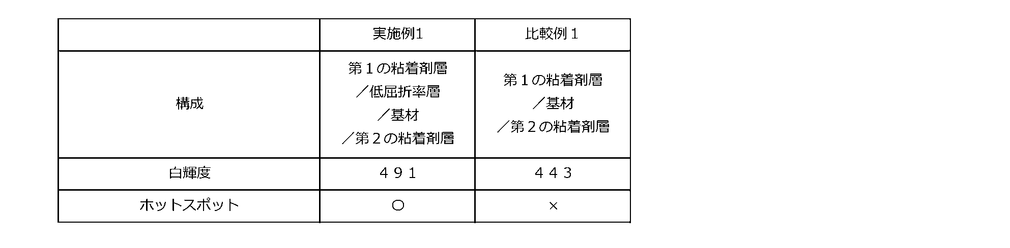
表1から明らかなように、本発明のLEDバックライト用フィルムを用いれば、入射光を効率よく導き得るLEDバックライトを得ることが出来る。
As is clear from Table 1, an LED backlight capable of efficiently guiding incident light can be obtained by using the film for LED backlight of the present invention.
10 第1の粘着剤層
20 低屈折率層
30 基材
40 第2の粘着剤層
100 導光ユニット
110 LEDバックライト用フィルム
130 LED光源
200 LEDバックライト DESCRIPTION OFSYMBOLS 10 1st adhesive layer 20 Low refractive index layer 30 Base material 40 2nd adhesive layer 100 Light guide unit 110 Film for LED backlight 130 LED light source 200 LED backlight
20 低屈折率層
30 基材
40 第2の粘着剤層
100 導光ユニット
110 LEDバックライト用フィルム
130 LED光源
200 LEDバックライト DESCRIPTION OF
Claims (7)
- 低屈折率層と、該低屈折率層の少なくとも片側に配置された第1の粘着剤層とを備え、
該低屈折率層の屈折率が、1.25以下である、
LEDバックライト用フィルム。 A low refractive index layer, and a first pressure-sensitive adhesive layer disposed on at least one side of the low refractive index layer,
The refractive index of the low refractive index layer is 1.25 or less.
Film for LED backlight. - 前記低屈折率層が、空隙を有する多孔体として構成される、請求項1に記載のLEDバックライト用フィルム。 The LED backlight film according to claim 1, wherein the low refractive index layer is configured as a porous body having voids.
- 前記低屈折率層の空隙率が、35体積%以下である、請求項2に記載のLEDバックライト用フィルム。 The film for LED backlight according to claim 2, wherein the porosity of the low refractive index layer is 35% by volume or less.
- 厚みが、100μm以下である、請求項1から3のいずれかに記載のLEDバックライト用フィルム。 The film for LED backlight according to any one of claims 1 to 3, wherein the thickness is 100 µm or less.
- 請求項1から4のいずれかに記載のLEDバックライト用フィルムと、導光板とを備え、
該LEDバックライト用フィルムが、
該導光板の導光方向端面の近傍に、貼着して配置され、
該導光板の導光方向においては、該導光板の片面の一部を覆うようにし、導光方向を含む面内で導光方向と垂直な方向においては、該導光板の該片面の全域を覆うようにして、該導光板に貼着されている、
導光ユニット。 An LED backlight film according to any one of claims 1 to 4, and a light guide plate,
The LED backlight film is
In the vicinity of the light guide direction end face of the light guide plate, it is disposed by sticking,
In the light guide direction of the light guide plate, a part of one side of the light guide plate is covered, and in a direction perpendicular to the light guide direction within the plane including the light guide direction, the entire area of the one side of the light guide plate is covered. Covered to the light guide plate,
Light guiding unit. - 請求項5に記載の導光ユニットと、前記導光板の前記LEDバックライト用フィルムが配置された側の端面に配置されたLED光源とを備える、
LEDバックライト。 The light guide unit according to claim 5, and an LED light source disposed on an end surface of the light guide plate on the side where the film for LED backlight is disposed,
LED backlight. - 前記LEDバックライト用フィルムの厚みが、{(LED光源の厚み-導光板の厚み)×50%}~{(LED光源の厚み-導光板の厚み)×100%}である、
請求項6に記載のLEDバックライト。 The LED backlight film has a thickness of {(LED light source thickness−light guide plate thickness) × 50%} to {(LED light source thickness−light guide plate thickness) × 100%}.
The LED backlight according to claim 6.
Priority Applications (5)
| Application Number | Priority Date | Filing Date | Title |
|---|---|---|---|
| EP19748048.6A EP3748221A4 (en) | 2018-02-02 | 2019-01-23 | Led backlight film and led backlight |
| CN201980010198.2A CN111656087A (en) | 2018-02-02 | 2019-01-23 | Film for LED backlight and LED backlight |
| JP2019569043A JPWO2019151073A1 (en) | 2018-02-02 | 2019-01-23 | LED backlight film, LED backlight |
| KR1020207021709A KR20200118009A (en) | 2018-02-02 | 2019-01-23 | LED backlight film, LED backlight |
| US16/937,131 US20200355866A1 (en) | 2018-02-02 | 2020-07-23 | Led backlight film and led backlight |
Applications Claiming Priority (2)
| Application Number | Priority Date | Filing Date | Title |
|---|---|---|---|
| JP2018017206 | 2018-02-02 | ||
| JP2018-017206 | 2018-02-02 |
Related Child Applications (1)
| Application Number | Title | Priority Date | Filing Date |
|---|---|---|---|
| US16/937,131 Continuation-In-Part US20200355866A1 (en) | 2018-02-02 | 2020-07-23 | Led backlight film and led backlight |
Publications (1)
| Publication Number | Publication Date |
|---|---|
| WO2019151073A1 true WO2019151073A1 (en) | 2019-08-08 |
Family
ID=67478722
Family Applications (1)
| Application Number | Title | Priority Date | Filing Date |
|---|---|---|---|
| PCT/JP2019/002036 WO2019151073A1 (en) | 2018-02-02 | 2019-01-23 | Led backlight film and led backlight |
Country Status (7)
| Country | Link |
|---|---|
| US (1) | US20200355866A1 (en) |
| EP (1) | EP3748221A4 (en) |
| JP (2) | JPWO2019151073A1 (en) |
| KR (1) | KR20200118009A (en) |
| CN (1) | CN111656087A (en) |
| TW (1) | TW201935113A (en) |
| WO (1) | WO2019151073A1 (en) |
Cited By (6)
| Publication number | Priority date | Publication date | Assignee | Title |
|---|---|---|---|---|
| WO2021193894A1 (en) * | 2020-03-27 | 2021-09-30 | 日東電工株式会社 | Illumination device |
| WO2021193896A1 (en) | 2020-03-27 | 2021-09-30 | 日東電工株式会社 | Backlight unit and image display device |
| WO2021193895A1 (en) | 2020-03-27 | 2021-09-30 | 日東電工株式会社 | Optical member and backlight unit using said optical member, and image display device |
| WO2021193789A1 (en) | 2020-03-26 | 2021-09-30 | 日東電工株式会社 | Optical member, and backlight unit and image display device using said optical member |
| WO2021193591A1 (en) | 2020-03-24 | 2021-09-30 | 日東電工株式会社 | Optical laminate with double-sided adhesive layer, and optical device |
| WO2021200770A1 (en) | 2020-03-30 | 2021-10-07 | 日東電工株式会社 | Backlight unit and image display device |
Families Citing this family (2)
| Publication number | Priority date | Publication date | Assignee | Title |
|---|---|---|---|---|
| DE112022003130T5 (en) | 2021-06-18 | 2024-04-11 | Rohm Co., Ltd. | TRANSDUCER AND ELECTRONIC DEVICE |
| JP2023150234A (en) * | 2022-03-31 | 2023-10-16 | 日東電工株式会社 | Optical laminate and method of manufacturing optical laminate |
Citations (9)
| Publication number | Priority date | Publication date | Assignee | Title |
|---|---|---|---|---|
| JPH09145903A (en) * | 1995-11-27 | 1997-06-06 | Dainippon Printing Co Ltd | Antireflection film |
| WO2004113966A1 (en) | 2003-06-18 | 2004-12-29 | Asahi Kasei Kabushiki Kaisha | Antireflective film |
| JP2006011175A (en) | 2004-06-28 | 2006-01-12 | Pentax Corp | Optical device having antireflection film and its manufacturing method |
| JP2008040171A (en) | 2006-08-07 | 2008-02-21 | Pentax Corp | Optical element with antireflection film having self-cleaning effect and method for manufacturing the same |
| JP2010189212A (en) | 2009-02-17 | 2010-09-02 | Shinshu Univ | Porous silica film and method for manufacturing the same |
| JP2011207751A (en) * | 2010-03-11 | 2011-10-20 | Mitsubishi Chemicals Corp | Method for producing porous siliceous film |
| JP2012059645A (en) * | 2010-09-10 | 2012-03-22 | Fujikura Ltd | Planar light-emitting device and lighting module |
| JP2012114284A (en) | 2010-11-25 | 2012-06-14 | Toshiba Corp | Led module and illuminating device |
| JP2017047677A (en) | 2015-07-31 | 2017-03-09 | 日東電工株式会社 | Optical laminate, method for manufacturing optical laminate, optical member, image display device, method for manufacturing optical member and method for manufacturing image display device |
Family Cites Families (9)
| Publication number | Priority date | Publication date | Assignee | Title |
|---|---|---|---|---|
| JPH03261988A (en) * | 1990-03-12 | 1991-11-21 | Sumitomo Chem Co Ltd | Face type light emitting body |
| KR20120115568A (en) * | 2010-02-10 | 2012-10-18 | 쓰리엠 이노베이티브 프로퍼티즈 컴파니 | Illumination device having viscoelastic layer |
| TWI534458B (en) * | 2010-10-20 | 2016-05-21 | 3M新設資產公司 | Protected low refractive index optical element |
| KR20130028270A (en) * | 2011-09-09 | 2013-03-19 | 엘지디스플레이 주식회사 | Reflecting sheet and method for manufacturing the same, liquid crystal display device including reflecting sheet |
| KR102064751B1 (en) * | 2014-02-27 | 2020-01-10 | 엘지디스플레이 주식회사 | Liquid crystal display device having minimized bezzel |
| CN106575059B (en) * | 2014-08-28 | 2021-03-19 | 索尼公司 | Display device and illumination device |
| JP2017064954A (en) * | 2015-09-28 | 2017-04-06 | 日東電工株式会社 | Method for producing laminated film and method for producing image display device |
| JP6809824B2 (en) * | 2016-07-04 | 2021-01-06 | 日東電工株式会社 | Manufacturing method of optical laminate and optical laminate intermediate |
| TWI587052B (en) * | 2016-07-18 | 2017-06-11 | 恆顥科技股份有限公司 | Light source module and display |
-
2019
- 2019-01-23 WO PCT/JP2019/002036 patent/WO2019151073A1/en unknown
- 2019-01-23 JP JP2019569043A patent/JPWO2019151073A1/en active Pending
- 2019-01-23 CN CN201980010198.2A patent/CN111656087A/en active Pending
- 2019-01-23 KR KR1020207021709A patent/KR20200118009A/en not_active Application Discontinuation
- 2019-01-23 EP EP19748048.6A patent/EP3748221A4/en active Pending
- 2019-01-25 TW TW108102907A patent/TW201935113A/en unknown
-
2020
- 2020-07-23 US US16/937,131 patent/US20200355866A1/en not_active Abandoned
-
2021
- 2021-04-09 JP JP2021066529A patent/JP7181961B2/en active Active
Patent Citations (9)
| Publication number | Priority date | Publication date | Assignee | Title |
|---|---|---|---|---|
| JPH09145903A (en) * | 1995-11-27 | 1997-06-06 | Dainippon Printing Co Ltd | Antireflection film |
| WO2004113966A1 (en) | 2003-06-18 | 2004-12-29 | Asahi Kasei Kabushiki Kaisha | Antireflective film |
| JP2006011175A (en) | 2004-06-28 | 2006-01-12 | Pentax Corp | Optical device having antireflection film and its manufacturing method |
| JP2008040171A (en) | 2006-08-07 | 2008-02-21 | Pentax Corp | Optical element with antireflection film having self-cleaning effect and method for manufacturing the same |
| JP2010189212A (en) | 2009-02-17 | 2010-09-02 | Shinshu Univ | Porous silica film and method for manufacturing the same |
| JP2011207751A (en) * | 2010-03-11 | 2011-10-20 | Mitsubishi Chemicals Corp | Method for producing porous siliceous film |
| JP2012059645A (en) * | 2010-09-10 | 2012-03-22 | Fujikura Ltd | Planar light-emitting device and lighting module |
| JP2012114284A (en) | 2010-11-25 | 2012-06-14 | Toshiba Corp | Led module and illuminating device |
| JP2017047677A (en) | 2015-07-31 | 2017-03-09 | 日東電工株式会社 | Optical laminate, method for manufacturing optical laminate, optical member, image display device, method for manufacturing optical member and method for manufacturing image display device |
Non-Patent Citations (1)
| Title |
|---|
| See also references of EP3748221A4 |
Cited By (12)
| Publication number | Priority date | Publication date | Assignee | Title |
|---|---|---|---|---|
| WO2021193591A1 (en) | 2020-03-24 | 2021-09-30 | 日東電工株式会社 | Optical laminate with double-sided adhesive layer, and optical device |
| WO2021193789A1 (en) | 2020-03-26 | 2021-09-30 | 日東電工株式会社 | Optical member, and backlight unit and image display device using said optical member |
| EP4130561A4 (en) * | 2020-03-26 | 2024-03-20 | Nitto Denko Corp | Optical member, and backlight unit and image display device using said optical member |
| WO2021193894A1 (en) * | 2020-03-27 | 2021-09-30 | 日東電工株式会社 | Illumination device |
| WO2021193896A1 (en) | 2020-03-27 | 2021-09-30 | 日東電工株式会社 | Backlight unit and image display device |
| WO2021193895A1 (en) | 2020-03-27 | 2021-09-30 | 日東電工株式会社 | Optical member and backlight unit using said optical member, and image display device |
| JPWO2021193894A1 (en) * | 2020-03-27 | 2021-09-30 | ||
| KR20220158708A (en) | 2020-03-27 | 2022-12-01 | 닛토덴코 가부시키가이샤 | Backlight unit and image display device |
| JP7425856B2 (en) | 2020-03-27 | 2024-01-31 | 日東電工株式会社 | lighting equipment |
| US11921311B2 (en) | 2020-03-27 | 2024-03-05 | Nitto Denko Corporation | Illumination device |
| EP4130546A4 (en) * | 2020-03-27 | 2024-04-03 | Nitto Denko Corp | Illumination device |
| WO2021200770A1 (en) | 2020-03-30 | 2021-10-07 | 日東電工株式会社 | Backlight unit and image display device |
Also Published As
| Publication number | Publication date |
|---|---|
| EP3748221A4 (en) | 2021-10-13 |
| JPWO2019151073A1 (en) | 2021-01-07 |
| TW201935113A (en) | 2019-09-01 |
| CN111656087A (en) | 2020-09-11 |
| KR20200118009A (en) | 2020-10-14 |
| JP2021101437A (en) | 2021-07-08 |
| JP7181961B2 (en) | 2022-12-01 |
| US20200355866A1 (en) | 2020-11-12 |
| EP3748221A1 (en) | 2020-12-09 |
Similar Documents
| Publication | Publication Date | Title |
|---|---|---|
| JP7181961B2 (en) | LED backlight film, LED backlight | |
| WO2019146628A1 (en) | Film for led lighting equipment, and led lighting equipment | |
| KR101610041B1 (en) | Printing sheet, decorative sheet, and adhesive decorative sheet | |
| JP5937694B2 (en) | Transparent double-sided adhesive sheet and image display device using the same | |
| JP6240793B2 (en) | Double-sided adhesive sheet for surface protection panel and surface protection panel | |
| JP2013510402A (en) | Backlight unit | |
| JP2013544931A (en) | Adhesive composition for touch panel, adhesive film and touch panel | |
| KR20120018171A (en) | Ultraviolet-curable adhesive agent composite, adhesive agent layer, adhesive sheet, and manufacturing method therefor | |
| TWI707023B (en) | Adhesive sheet | |
| TW201723115A (en) | Solventless adhesive composition, adhesive, adhesive sheet and display capable of exhibiting excellent blister resistance | |
| JP2015157913A (en) | Adhesive composition for optical use, adhesive sheet for optical sheet, and optical laminate | |
| JP6094226B2 (en) | Protective adhesive film, screen panel and touch panel | |
| JP2019077747A (en) | Pressure-sensitive adhesive sheet, method of manufacturing laminate and laminate | |
| JP2014084337A (en) | Protective adhesive film | |
| JP2021021034A (en) | Adhesive sheet, backlight unit and liquid crystal display device | |
| JP6083463B2 (en) | Conductive laminate, bubble or crack occurrence reducing sheet, and bubble or crack occurrence reducing method | |
| TW202007740A (en) | Adhesive sheet and laminate body having an adhesive layer containing an antistatic agent with excellent foam resistance | |
| JP7425856B2 (en) | lighting equipment | |
| JP7112227B2 (en) | Acrylic pressure-sensitive adhesive composition and pressure-sensitive adhesive sheet | |
| JP2019031621A (en) | Optical adhesive sheet, flexible touch panel and flexible display device | |
| EP4309888A1 (en) | Optical laminate, optical laminate production method, optical member, optical device, optical member production method and optical device production method | |
| JP2011191428A (en) | Reflection preventing film | |
| TWI751244B (en) | Solvent-free adhesive composition, adhesive plate and display body | |
| JP2022131866A (en) | Adhesive sheet, laminate, and optical device and image display device | |
| JP2014018998A (en) | Conductive laminated body, sheet for reducing generation of air bubble or crack, and method for reducing generation of air bubble or crack |
Legal Events
| Date | Code | Title | Description |
|---|---|---|---|
| 121 | Ep: the epo has been informed by wipo that ep was designated in this application |
Ref document number: 19748048 Country of ref document: EP Kind code of ref document: A1 |
|
| ENP | Entry into the national phase |
Ref document number: 2019569043 Country of ref document: JP Kind code of ref document: A |
|
| NENP | Non-entry into the national phase |
Ref country code: DE |
|
| ENP | Entry into the national phase |
Ref document number: 2019748048 Country of ref document: EP Effective date: 20200902 |