WO2019150449A1 - 半導体装置の製造方法、及びフィルム状接着剤 - Google Patents
半導体装置の製造方法、及びフィルム状接着剤 Download PDFInfo
- Publication number
- WO2019150449A1 WO2019150449A1 PCT/JP2018/003028 JP2018003028W WO2019150449A1 WO 2019150449 A1 WO2019150449 A1 WO 2019150449A1 JP 2018003028 W JP2018003028 W JP 2018003028W WO 2019150449 A1 WO2019150449 A1 WO 2019150449A1
- Authority
- WO
- WIPO (PCT)
- Prior art keywords
- film
- adhesive
- semiconductor element
- component
- film adhesive
- Prior art date
- Legal status (The legal status is an assumption and is not a legal conclusion. Google has not performed a legal analysis and makes no representation as to the accuracy of the status listed.)
- Ceased
Links
Images



Classifications
-
- H—ELECTRICITY
- H10—SEMICONDUCTOR DEVICES; ELECTRIC SOLID-STATE DEVICES NOT OTHERWISE PROVIDED FOR
- H10W—GENERIC PACKAGES, INTERCONNECTIONS, CONNECTORS OR OTHER CONSTRUCTIONAL DETAILS OF DEVICES COVERED BY CLASS H10
- H10W72/00—Interconnections or connectors in packages
- H10W72/071—Connecting or disconnecting
- H10W72/073—Connecting or disconnecting of die-attach connectors
-
- C—CHEMISTRY; METALLURGY
- C09—DYES; PAINTS; POLISHES; NATURAL RESINS; ADHESIVES; COMPOSITIONS NOT OTHERWISE PROVIDED FOR; APPLICATIONS OF MATERIALS NOT OTHERWISE PROVIDED FOR
- C09J—ADHESIVES; NON-MECHANICAL ASPECTS OF ADHESIVE PROCESSES IN GENERAL; ADHESIVE PROCESSES NOT PROVIDED FOR ELSEWHERE; USE OF MATERIALS AS ADHESIVES
- C09J11/00—Features of adhesives not provided for in group C09J9/00, e.g. additives
-
- C—CHEMISTRY; METALLURGY
- C09—DYES; PAINTS; POLISHES; NATURAL RESINS; ADHESIVES; COMPOSITIONS NOT OTHERWISE PROVIDED FOR; APPLICATIONS OF MATERIALS NOT OTHERWISE PROVIDED FOR
- C09J—ADHESIVES; NON-MECHANICAL ASPECTS OF ADHESIVE PROCESSES IN GENERAL; ADHESIVE PROCESSES NOT PROVIDED FOR ELSEWHERE; USE OF MATERIALS AS ADHESIVES
- C09J11/00—Features of adhesives not provided for in group C09J9/00, e.g. additives
- C09J11/02—Non-macromolecular additives
- C09J11/04—Non-macromolecular additives inorganic
-
- C—CHEMISTRY; METALLURGY
- C09—DYES; PAINTS; POLISHES; NATURAL RESINS; ADHESIVES; COMPOSITIONS NOT OTHERWISE PROVIDED FOR; APPLICATIONS OF MATERIALS NOT OTHERWISE PROVIDED FOR
- C09J—ADHESIVES; NON-MECHANICAL ASPECTS OF ADHESIVE PROCESSES IN GENERAL; ADHESIVE PROCESSES NOT PROVIDED FOR ELSEWHERE; USE OF MATERIALS AS ADHESIVES
- C09J133/00—Adhesives based on homopolymers or copolymers of compounds having one or more unsaturated aliphatic radicals, each having only one carbon-to-carbon double bond, and at least one being terminated by only one carboxyl radical, or of salts, anhydrides, esters, amides, imides, or nitriles thereof; Adhesives based on derivatives of such polymers
-
- C—CHEMISTRY; METALLURGY
- C09—DYES; PAINTS; POLISHES; NATURAL RESINS; ADHESIVES; COMPOSITIONS NOT OTHERWISE PROVIDED FOR; APPLICATIONS OF MATERIALS NOT OTHERWISE PROVIDED FOR
- C09J—ADHESIVES; NON-MECHANICAL ASPECTS OF ADHESIVE PROCESSES IN GENERAL; ADHESIVE PROCESSES NOT PROVIDED FOR ELSEWHERE; USE OF MATERIALS AS ADHESIVES
- C09J133/00—Adhesives based on homopolymers or copolymers of compounds having one or more unsaturated aliphatic radicals, each having only one carbon-to-carbon double bond, and at least one being terminated by only one carboxyl radical, or of salts, anhydrides, esters, amides, imides, or nitriles thereof; Adhesives based on derivatives of such polymers
- C09J133/04—Homopolymers or copolymers of esters
-
- C—CHEMISTRY; METALLURGY
- C09—DYES; PAINTS; POLISHES; NATURAL RESINS; ADHESIVES; COMPOSITIONS NOT OTHERWISE PROVIDED FOR; APPLICATIONS OF MATERIALS NOT OTHERWISE PROVIDED FOR
- C09J—ADHESIVES; NON-MECHANICAL ASPECTS OF ADHESIVE PROCESSES IN GENERAL; ADHESIVE PROCESSES NOT PROVIDED FOR ELSEWHERE; USE OF MATERIALS AS ADHESIVES
- C09J163/00—Adhesives based on epoxy resins; Adhesives based on derivatives of epoxy resins
-
- C—CHEMISTRY; METALLURGY
- C09—DYES; PAINTS; POLISHES; NATURAL RESINS; ADHESIVES; COMPOSITIONS NOT OTHERWISE PROVIDED FOR; APPLICATIONS OF MATERIALS NOT OTHERWISE PROVIDED FOR
- C09J—ADHESIVES; NON-MECHANICAL ASPECTS OF ADHESIVE PROCESSES IN GENERAL; ADHESIVE PROCESSES NOT PROVIDED FOR ELSEWHERE; USE OF MATERIALS AS ADHESIVES
- C09J7/00—Adhesives in the form of films or foils
-
- C—CHEMISTRY; METALLURGY
- C09—DYES; PAINTS; POLISHES; NATURAL RESINS; ADHESIVES; COMPOSITIONS NOT OTHERWISE PROVIDED FOR; APPLICATIONS OF MATERIALS NOT OTHERWISE PROVIDED FOR
- C09J—ADHESIVES; NON-MECHANICAL ASPECTS OF ADHESIVE PROCESSES IN GENERAL; ADHESIVE PROCESSES NOT PROVIDED FOR ELSEWHERE; USE OF MATERIALS AS ADHESIVES
- C09J7/00—Adhesives in the form of films or foils
- C09J7/20—Adhesives in the form of films or foils characterised by their carriers
-
- H—ELECTRICITY
- H10—SEMICONDUCTOR DEVICES; ELECTRIC SOLID-STATE DEVICES NOT OTHERWISE PROVIDED FOR
- H10W—GENERIC PACKAGES, INTERCONNECTIONS, CONNECTORS OR OTHER CONSTRUCTIONAL DETAILS OF DEVICES COVERED BY CLASS H10
- H10W72/00—Interconnections or connectors in packages
- H10W72/071—Connecting or disconnecting
-
- H—ELECTRICITY
- H10—SEMICONDUCTOR DEVICES; ELECTRIC SOLID-STATE DEVICES NOT OTHERWISE PROVIDED FOR
- H10W—GENERIC PACKAGES, INTERCONNECTIONS, CONNECTORS OR OTHER CONSTRUCTIONAL DETAILS OF DEVICES COVERED BY CLASS H10
- H10W72/00—Interconnections or connectors in packages
- H10W72/50—Bond wires
-
- H—ELECTRICITY
- H10—SEMICONDUCTOR DEVICES; ELECTRIC SOLID-STATE DEVICES NOT OTHERWISE PROVIDED FOR
- H10W—GENERIC PACKAGES, INTERCONNECTIONS, CONNECTORS OR OTHER CONSTRUCTIONAL DETAILS OF DEVICES COVERED BY CLASS H10
- H10W74/00—Encapsulations, e.g. protective coatings
- H10W74/10—Encapsulations, e.g. protective coatings characterised by their shape or disposition
-
- H—ELECTRICITY
- H10—SEMICONDUCTOR DEVICES; ELECTRIC SOLID-STATE DEVICES NOT OTHERWISE PROVIDED FOR
- H10W—GENERIC PACKAGES, INTERCONNECTIONS, CONNECTORS OR OTHER CONSTRUCTIONAL DETAILS OF DEVICES COVERED BY CLASS H10
- H10W74/00—Encapsulations, e.g. protective coatings
- H10W74/40—Encapsulations, e.g. protective coatings characterised by their materials
-
- H—ELECTRICITY
- H10—SEMICONDUCTOR DEVICES; ELECTRIC SOLID-STATE DEVICES NOT OTHERWISE PROVIDED FOR
- H10W—GENERIC PACKAGES, INTERCONNECTIONS, CONNECTORS OR OTHER CONSTRUCTIONAL DETAILS OF DEVICES COVERED BY CLASS H10
- H10W90/00—Package configurations
-
- H—ELECTRICITY
- H10—SEMICONDUCTOR DEVICES; ELECTRIC SOLID-STATE DEVICES NOT OTHERWISE PROVIDED FOR
- H10W—GENERIC PACKAGES, INTERCONNECTIONS, CONNECTORS OR OTHER CONSTRUCTIONAL DETAILS OF DEVICES COVERED BY CLASS H10
- H10W95/00—Packaging processes not covered by the other groups of this subclass
-
- C—CHEMISTRY; METALLURGY
- C09—DYES; PAINTS; POLISHES; NATURAL RESINS; ADHESIVES; COMPOSITIONS NOT OTHERWISE PROVIDED FOR; APPLICATIONS OF MATERIALS NOT OTHERWISE PROVIDED FOR
- C09J—ADHESIVES; NON-MECHANICAL ASPECTS OF ADHESIVE PROCESSES IN GENERAL; ADHESIVE PROCESSES NOT PROVIDED FOR ELSEWHERE; USE OF MATERIALS AS ADHESIVES
- C09J2203/00—Applications of adhesives in processes or use of adhesives in the form of films or foils
- C09J2203/326—Applications of adhesives in processes or use of adhesives in the form of films or foils for bonding electronic components such as wafers, chips or semiconductors
-
- C—CHEMISTRY; METALLURGY
- C09—DYES; PAINTS; POLISHES; NATURAL RESINS; ADHESIVES; COMPOSITIONS NOT OTHERWISE PROVIDED FOR; APPLICATIONS OF MATERIALS NOT OTHERWISE PROVIDED FOR
- C09J—ADHESIVES; NON-MECHANICAL ASPECTS OF ADHESIVE PROCESSES IN GENERAL; ADHESIVE PROCESSES NOT PROVIDED FOR ELSEWHERE; USE OF MATERIALS AS ADHESIVES
- C09J2301/00—Additional features of adhesives in the form of films or foils
- C09J2301/30—Additional features of adhesives in the form of films or foils characterized by the chemical, physicochemical or physical properties of the adhesive or the carrier
- C09J2301/312—Additional features of adhesives in the form of films or foils characterized by the chemical, physicochemical or physical properties of the adhesive or the carrier parameters being the characterizing feature
-
- H—ELECTRICITY
- H10—SEMICONDUCTOR DEVICES; ELECTRIC SOLID-STATE DEVICES NOT OTHERWISE PROVIDED FOR
- H10W—GENERIC PACKAGES, INTERCONNECTIONS, CONNECTORS OR OTHER CONSTRUCTIONAL DETAILS OF DEVICES COVERED BY CLASS H10
- H10W72/00—Interconnections or connectors in packages
- H10W72/071—Connecting or disconnecting
- H10W72/075—Connecting or disconnecting of bond wires
-
- H—ELECTRICITY
- H10—SEMICONDUCTOR DEVICES; ELECTRIC SOLID-STATE DEVICES NOT OTHERWISE PROVIDED FOR
- H10W—GENERIC PACKAGES, INTERCONNECTIONS, CONNECTORS OR OTHER CONSTRUCTIONAL DETAILS OF DEVICES COVERED BY CLASS H10
- H10W72/00—Interconnections or connectors in packages
- H10W72/50—Bond wires
- H10W72/531—Shapes of wire connectors
- H10W72/5363—Shapes of wire connectors the connected ends being wedge-shaped
-
- H—ELECTRICITY
- H10—SEMICONDUCTOR DEVICES; ELECTRIC SOLID-STATE DEVICES NOT OTHERWISE PROVIDED FOR
- H10W—GENERIC PACKAGES, INTERCONNECTIONS, CONNECTORS OR OTHER CONSTRUCTIONAL DETAILS OF DEVICES COVERED BY CLASS H10
- H10W72/00—Interconnections or connectors in packages
- H10W72/851—Dispositions of multiple connectors or interconnections
- H10W72/874—On different surfaces
- H10W72/884—Die-attach connectors and bond wires
-
- H—ELECTRICITY
- H10—SEMICONDUCTOR DEVICES; ELECTRIC SOLID-STATE DEVICES NOT OTHERWISE PROVIDED FOR
- H10W—GENERIC PACKAGES, INTERCONNECTIONS, CONNECTORS OR OTHER CONSTRUCTIONAL DETAILS OF DEVICES COVERED BY CLASS H10
- H10W74/00—Encapsulations, e.g. protective coatings
-
- H—ELECTRICITY
- H10—SEMICONDUCTOR DEVICES; ELECTRIC SOLID-STATE DEVICES NOT OTHERWISE PROVIDED FOR
- H10W—GENERIC PACKAGES, INTERCONNECTIONS, CONNECTORS OR OTHER CONSTRUCTIONAL DETAILS OF DEVICES COVERED BY CLASS H10
- H10W90/00—Package configurations
- H10W90/701—Package configurations characterised by the relative positions of pads or connectors relative to package parts
- H10W90/731—Package configurations characterised by the relative positions of pads or connectors relative to package parts of die-attach connectors
- H10W90/732—Package configurations characterised by the relative positions of pads or connectors relative to package parts of die-attach connectors between stacked chips
Definitions
- the present invention relates to a method for manufacturing a semiconductor device and a film adhesive.
- Adhesive sheets are known that can provide a wire embedded semiconductor device capable of filling irregularities due to wiring of a substrate in a semiconductor device, wires attached to a semiconductor chip, and the like (for example, Patent Documents 1 and 2). .
- the adhesive sheet contains a thermosetting component as a main component in order to exhibit high fluidity when filling unevenness.
- a controller chip for controlling the operation of the semiconductor device has been arranged at the top of the stacked semiconductor elements.
- the semiconductor device packaging technology has a controller chip arranged at the bottom.
- the film adhesive used when crimping the second-stage semiconductor element is thickened, and the controller chip is placed inside the film adhesive. Embed packages are attracting attention.
- the film adhesive used for such applications requires high fluidity that can embed a controller chip, a wire connected to the controller chip, a step due to unevenness on the substrate surface, and the like.
- the present invention provides a first die-bonding step for electrically connecting a first semiconductor element on a substrate via a first wire, and a second semiconductor element having a larger area than the first semiconductor element.
- a second die-bonding step of embedding the first wire and the first semiconductor element in the film-like adhesive by pressing the film-like adhesive so as to cover the film.
- the present invention it is possible to obtain a semiconductor device excellent in connection reliability while suppressing an increase in lead time. More specifically, by using a film adhesive having a shear modulus at 150 ° C. of 1.5 MPa or less, voids generated in the second die-bonding process are caused by a sealing process which is a subsequent process. Can be resolved. This eliminates the need for a special process for eliminating the air gap, and does not increase the lead time.
- the shear modulus at 150 ° C. means that the film-like adhesive is heated from room temperature to 125 ° C. at a heating rate of 5 ° C./min and held for 1 hour while applying a strain of 5% at a frequency of 1 Hz. Then, the temperature is further raised to 150 ° C. at a rate of temperature rise of 5 ° C./min and held for 45 minutes, and then measured using a dynamic viscoelasticity measuring device.
- the film-like adhesive preferably has a tensile elastic modulus at 170 to 190 ° C. after curing of 15 MPa or less. Since the film adhesive has low elasticity after curing, it becomes possible to obtain good embedding properties and stress relaxation properties during the sealing process. For example, even when a thin second semiconductor element is used, warping of the semiconductor device after the film adhesive is cured can be suppressed. Thereby, the stress of the semiconductor device is relaxed, and it becomes easy to obtain a semiconductor device exhibiting good connection reliability.
- the shear viscosity at 80 ° C. of the film adhesive is 15000 Pa ⁇ s or less. This makes it easy to obtain good embedding properties.
- the film adhesive preferably contains an acrylic resin and an epoxy resin.
- the acrylic resin includes a first acrylic resin having a weight average molecular weight of 100,000 to 500,000 and a second acrylic resin having a weight average molecular weight of 600,000 to 1,000,000.
- the content of the first acrylic resin is preferably 50% by mass or more based on the mass.
- the film adhesive contains at least one of an inorganic filler and an organic filler.
- the first semiconductor element is electrically connected to the substrate via the first wire
- the second semiconductor element has a second area larger than the area of the first semiconductor element on the first semiconductor element.
- the shear modulus at 150 ° C. is 1.5 MPa or less, which is used for pressure-bonding the second semiconductor element and embedding the first wire and the first semiconductor element.
- a film adhesive is provided. By using the film adhesive of the present invention, it is possible to obtain a semiconductor device having excellent connection reliability while suppressing an increase in lead time.
- the tensile modulus at 170 to 190 ° C. after curing is preferably 15 MPa or less.
- the shear viscosity at 80 ° C. is preferably 15000 Pa ⁇ s or less.
- the film adhesive of the present invention preferably contains an acrylic resin and an epoxy resin.
- the acrylic resin contains a first acrylic resin having a weight average molecular weight of 100,000 to 500,000 and a second acrylic resin having a weight average molecular weight of 600,000 to 1,000,000.
- the content of the first acrylic resin is preferably 50% by mass or more based on the total mass of the acrylic resin.
- the film adhesive of the present invention preferably contains at least one of an inorganic filler and an organic filler.
- the present invention it is possible to provide a semiconductor device manufacturing method capable of obtaining a semiconductor device excellent in connection reliability while suppressing an increase in lead time. Moreover, according to this invention, the film adhesive used for the said manufacturing method can be provided.
- FIG. 8 is a diagram showing a step subsequent to FIG. 7.
- FIG. 9 is a diagram showing a step subsequent to that in FIG. 8.
- FIG. 10 is a diagram showing a step subsequent to FIG. 9.
- FIG. 11 is a diagram showing a step subsequent to FIG. 10.
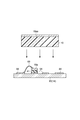
- FIG. 1 is a cross-sectional view schematically showing a film adhesive 10 according to the present embodiment.
- the film-like adhesive 10 is thermosetting, and is formed by forming an adhesive composition that can be in a completely cured product (C stage) state after a curing process through a semi-cured (B stage) state into a film shape. is there.
- the film adhesive 10 has a shear elastic modulus at 150 ° C. of 1.5 MPa or less.
- the shear modulus is preferably 1.2 MPa or less, more preferably 1.0 MPa or less, More preferably, it is 0.8 MPa or less.
- the lower limit of the shear modulus is not particularly limited, but can be set to 0.01 MPa from the viewpoint of suppressing excessive fluidity.
- the shear modulus can be adjusted by adjusting the types and amounts of the components (a) to (f) as described later. For example, as a guideline for reducing the shear modulus at 150 ° C.
- the film-like adhesive 10 preferably has a tensile elastic modulus at 170 to 190 ° C. after curing of 15 MPa or less.
- the tensile elastic modulus is more preferably 12 MPa or less, further preferably 10 MPa or less, and particularly preferably 8 MPa or less.
- the lower limit of the tensile elastic modulus is not particularly limited, but can be set to 1 MPa from the viewpoint of securing appropriate adhesiveness.
- the tensile elastic modulus can be measured using a dynamic viscoelasticity measuring apparatus with a frequency of 10 Hz, for example.
- the film adhesive 10 preferably has a shear viscosity at 80 ° C. of 15000 Pa ⁇ s or less. From the viewpoint of easily obtaining good embedding properties, the shear viscosity is more preferably 10,000 Pa ⁇ s or less, and further preferably 9000 Pa ⁇ s or less. The lower limit of the shear viscosity is not particularly limited, but can be set to 1000 Pa ⁇ s from the viewpoint of suppressing excessive fluidity. The shear viscosity can be measured using, for example, a dynamic viscoelasticity measuring apparatus.
- the content component of the film adhesive 10 is not specifically limited, For example, (a) thermosetting component, (b) thermoplastic component, (c) inorganic filler, (d) organic filler, (e) curing accelerator, (F) Other components can be included.
- the characteristics of the film adhesive 10 can be adjusted by adjusting the types and amounts of these components (a) to (f).
- thermosetting component A thermosetting resin is mentioned as a thermosetting component.
- an epoxy resin, a phenol resin, or the like is preferable as the thermosetting component.
- epoxy resin generally known epoxy resins such as an aromatic ring-containing epoxy resin, a heterocyclic ring-containing epoxy resin, and an alicyclic epoxy resin can be used.
- the epoxy resin may be a polyfunctional epoxy resin.
- Specific examples of epoxy resins include bisphenol A type epoxy resins, bisphenol F type epoxy resins, bisphenol E type epoxy resins, bifunctional epoxy resins obtained by modifying these bisphenol type epoxy resins, and cresol novolac type epoxy resins.
- Bisphenol A novolac type epoxy resin, fluorene modified epoxy resin, triphenylmethane type epoxy resin, biphenyl type epoxy resin, glycidylamine type epoxy resin, naphthalene modified epoxy resin and the like can be used.
- epoxy resin examples include YDF series and YDCN series manufactured by Nippon Kayaku Epoxy Manufacturing Co., Ltd., EPOX-MK series and VG-3101L manufactured by Printec Co., Ltd., and the like.
- the phenol resin examples include novolak type phenol resin, sylock type phenol resin, biphenyl type phenol resin, triphenylmethane type phenol resin, and modified phenol resin in which hydrogen on the phenol ring is substituted with an aryl group.
- a phenol resin from the viewpoint of heat resistance, the water absorption after introduction into a constant temperature and humidity chamber of 85 ° C. and 85% RH for 48 hours is 2% by mass or less, and 350 measured by a thermogravimetric analyzer (TGA). It is preferable that the heating mass reduction rate (temperature increase rate: 5 ° C./min, atmosphere: nitrogen) at 5 ° C. is less than 5 mass%.
- phenol resin examples include Phenolite KA and TD series manufactured by DIC Corporation, and HE series manufactured by Air Water Corporation.
- the compounding ratio of the epoxy resin and the phenol resin is 0.70 / 0.30 to 0.30 / 0.70 is preferable, 0.65 / 0.35 to 0.35 / 0.65 is more preferable, and 0.60 / 0.40 to 0.40 / 0.60 is preferable. More preferred is 0.60 / 0.40 to 0.50 / 0.50. It becomes easy to obtain the film adhesive 10 which has the outstanding sclerosis
- thermosetting resins having different curing speeds from the viewpoint of suppressing warpage of the semiconductor device after curing.
- the epoxy resins and phenol resins exemplified above for example, (a1) those having a softening point of 60 ° C. or lower or liquid at room temperature (no particular limitation as long as they are cured and have an adhesive action) And (a2) those having a softening point exceeding 60 ° C. (solid at normal temperature) are preferably used in combination.
- the normal temperature here means 5 to 35 ° C.
- the content of the component (a1) is preferably 10 to 50% by mass, more preferably 20 to 40% by mass based on the total mass of the component (a). This makes it easy to achieve both embeddability and process suitability such as dicing and pickup.
- the content of the component (a2) is preferably 10% by mass or more, more preferably 15% by mass or more based on the total mass of the component (a). Thereby, it becomes easy to adjust film forming property, fluidity
- the upper limit of content of (a2) component is not specifically limited, It can be 90 mass% on the basis of the total mass of (a) component.
- Thermoplastic component includes a thermoplastic component having a high monomer ratio having a crosslinkable functional group and a low molecular weight, and a thermoplastic component having a low monomer ratio having a crosslinkable functional group and a high molecular weight.
- the component (b) has (b1) a monomer unit having a crosslinkable functional group in an amount of 5 to 15 mol% based on the total amount of the monomer unit, a weight average molecular weight of 100,000 to 500,000, and a glass transition temperature Tg of ⁇ Glass component having a thermoplastic component having a temperature of 50 to 50 ° C.
- the component (b) is preferably an acrylic resin (acrylic resin) which is a thermoplastic resin, and further has a glass transition temperature Tg of ⁇ 50 ° C. to 50 ° C., and an epoxy group or glycidyl group such as glycidyl acrylate or glycidyl methacrylate.
- An acrylic resin such as an epoxy group-containing (meth) acrylic copolymer obtained by polymerizing a functional monomer having a crosslinkable functional group is more preferred.
- Epoxy group-containing acrylic rubber is an acrylic rubber having an epoxy group, which is mainly composed of an acrylate ester, and mainly composed of a copolymer such as butyl acrylate and acrylonitrile, a copolymer such as ethyl acrylate and acrylonitrile, or the like. is there.
- the crosslinkable functional group of component (b) includes crosslinkable functional groups such as alcoholic or phenolic hydroxyl groups and carboxyl groups in addition to epoxy groups.
- the monomer unit having a crosslinkable functional group is 5 to 15 mol% with respect to the total amount of the monomer unit from the viewpoint of easily exhibiting high adhesive force and easily reducing the shear modulus at 150 ° C. Is preferable, and 5 to 10 mol% is more preferable.
- the monomer unit having a crosslinkable functional group is preferably 1 to 7 mol% based on the total amount of the monomer units. 5 mol% is more preferable.
- the weight average molecular weight of the component (first acrylic resin) is preferably 100,000 to 500,000.
- the weight average molecular weight of the component (b1) is 100,000 or more, the film-forming property becomes better, and the adhesive strength and heat resistance of the film adhesive 10 can be further improved.
- the weight average molecular weight of the component (b1) is 500,000 or less, the shear viscosity is easily reduced, so that the embedding property of the film adhesive 10 becomes better.
- the weight average molecular weight of the component (b2) (second acrylic resin) is preferably 600,000 to 1,000,000.
- the weight average molecular weight of the component (b2) is 600,000 or more, the effect of improving the film formability is further improved by the combined use with the component (b1).
- the weight average molecular weight of the component (b2) is 1,000,000 or less, the shear viscosity of the uncured film adhesive 10 can be easily reduced, so that the embedding property becomes better.
- the machinability of the uncured film adhesive 10 may be improved, and the quality of dicing may be improved.
- the weight average molecular weight is a polystyrene conversion value obtained by a gel permeation chromatography method (GPC) using a calibration curve with standard polystyrene.
- the glass transition temperature Tg of the component (b1) and the component (b2) is preferably ⁇ 50 to 50 ° C.
- the flexibility of the film adhesive 10 becomes better.
- the glass transition temperature Tg is ⁇ 50 ° C. or higher, the flexibility of the film adhesive 10 does not become too high, so that the film adhesive 10 is easily cut when dicing the semiconductor wafer. For this reason, it is easy to suppress deterioration of dicing properties due to the generation of burrs.
- the glass transition temperature Tg of the entire component is preferably ⁇ 20 ° C. to 40 ° C., and preferably ⁇ 10 ° C. to 30 ° C.
- the glass transition temperature Tg can be measured using a thermal differential scanning calorimeter (for example, “Thermo Plus 2” manufactured by Rigaku Corporation).
- the component (b1) includes acrylic rubber HTR-860P-30B-CHN (trade name, manufactured by Nagase ChemteX Corporation). This compound has a glycidyl moiety as a crosslinkable moiety and is based on an acrylic rubber made of an acrylic acid derivative, and has a weight average molecular weight of 230,000 and a glass transition temperature Tg of ⁇ 7 ° C.
- the component (b2) include acrylic rubber HTR-860P-3CSP (trade name, manufactured by Nagase ChemteX Corporation).
- the content of the component (b1) (first acrylic resin) is preferably 50% by mass or more and more preferably 70% by mass or more based on the total mass of the component (b) (acrylic resin). . Thereby, it becomes easy to obtain good embedding properties, stress relaxation properties, film forming properties, adhesive properties, and the like.
- the upper limit of content of (b1) component is not specifically limited, It can be 90 mass% on the basis of the total mass of (b) component.
- the content of the component (b2) is preferably 10% by mass or more, more preferably 30% by mass or more based on the total mass of the component (b). Thereby, it becomes easy to adjust film forming property, adhesiveness, elastic modulus, and the like.
- the upper limit of content of (b2) component is not specifically limited, It can be 50 mass% on the basis of the total mass of (b) component.
- the content of the component (b) is preferably 20 to 160 parts by mass, and more preferably 50 to 120 parts by mass when the component (a) is 100 parts by mass.
- the content of the component (b) is not less than the above lower limit value, good film forming property, embedding property, adhesion property, stress relaxation property and the like are easily obtained.
- the content of the component (b) is not more than the above upper limit value, it becomes easy to obtain good film forming property, embedding property and the like.
- Inorganic filler As component, the dicing property of the film-like adhesive 10 in the B-stage state, the handling property of the film-like adhesive 10 is improved, the thermal conductivity is improved, the shear viscosity (melt viscosity) From the viewpoints of adjusting the thickness, imparting thixotropic properties, improving adhesive strength, and the like, silica filler and the like are preferable.
- the component (c) preferably contains two or more kinds of fillers having different average particle diameters for the purpose of improving the dicing property of the uncured film adhesive 10 and sufficiently expressing the cured adhesive force.
- the component (c) includes, for example, (c1) a first filler having an average particle size of 0.2 ⁇ m or more for the purpose of improving the dicing property of the uncured film adhesive 10, and (c2) adhesive force after curing. It is preferable to include a second filler having an average particle size of less than 0.2 ⁇ m for the purpose of fully expressing the above.
- the average particle diameter is a value obtained when analysis is performed using acetone as a solvent with a laser diffraction particle size distribution analyzer. It is more preferable that the difference between the average particle diameters of the first and second fillers is so large that it can be determined that the respective fillers are contained when analyzed by a particle size distribution measuring apparatus.
- the content of the component (c1) is preferably 30% by mass or more based on the total mass of the component (c).
- the content of the component (c1) is 30% by mass or more, it becomes easy to suppress deterioration of the film breakability and deterioration of the fluidity of the uncured film adhesive 10.
- the upper limit of content of (c1) component is not specifically limited, It can be 95 mass% on the basis of the total mass of (c) component.
- the content of the component (c2) is preferably 5% by mass or more based on the total mass of the component (c).
- (C2) It is easy to improve the adhesive force after hardening because content of a component is 5 mass% or more.
- the upper limit of content of (c2) component can be 30 mass% on the basis of the total mass of (c) component from a viewpoint of ensuring appropriate fluidity
- the content of the component (c) is preferably 10 to 90 parts by mass when the component (a) is 100 parts by mass.
- (C) When content of a component is more than the said lower limit, there exists a tendency for it to be easy to suppress the deterioration of the dicing property of the uncured film adhesive 10, and the fall of the adhesive force after hardening. On the other hand, when the content of the component (c) is not more than the above upper limit value, there is a tendency that it is easy to suppress a decrease in fluidity of the uncured film adhesive 10 and an increase in the elastic modulus after curing.
- the dicing property of the film adhesive 10 is improved, the handling property of the film adhesive 10 is improved, the shear viscosity (melt viscosity) is adjusted, the adhesive force is improved, and after curing.
- the shear viscosity melting viscosity
- the average particle diameter of the component (d) is preferably 0.2 ⁇ m or less from the viewpoint of sufficiently expressing the adhesive strength after curing.
- the content of the component (d) is preferably 0 to 50 parts by mass when the component (c) is 100 parts by mass.
- (E) Curing accelerator For the purpose of obtaining good curability, it is preferable to use (e) a curing accelerator.
- the component (e) is preferably an imidazole compound from the viewpoint of reactivity.
- the reactivity of (e) component is too high, not only will shear viscosity rise easily by the heating in the manufacturing process of the film adhesive 10, but it will tend to cause deterioration over time.
- the reactivity of the component (e) is too low, the curability of the film adhesive 10 tends to decrease. If the film adhesive 10 is mounted in a product without being sufficiently cured, sufficient adhesiveness may not be obtained, and the connection reliability of the semiconductor device may be deteriorated.
- hardenability of the film adhesive 10 improves more.
- the content of the component (e) is preferably 0 to 0.20 parts by mass when the component (a) is 100 parts by mass.
- (F) Other components
- a coupling agent examples include ⁇ -ureidopropyltriethoxysilane, ⁇ -mercaptopropyltrimethoxysilane, 3-phenylaminopropyltrimethoxysilane, 3- (2-aminoethyl) aminopropyltrimethoxysilane, and the like.
- the film adhesive 10 includes, for example, a step of forming a varnish layer by applying a varnish of an adhesive composition containing the above components on a base film, a step of removing the solvent from the varnish layer by heating and drying, It can be obtained by the step of removing the material film.
- the varnish can be prepared by mixing, kneading, etc. an adhesive composition containing the above components in an organic solvent.
- a dispersing machine such as a normal stirrer, a raking machine, a three-roller, or a ball mill can be used. These devices can be used in appropriate combination.
- the varnish can be applied by, for example, a comma coater or a die coater.
- the heating and drying conditions for the varnish are not particularly limited as long as the organic solvent used is sufficiently volatilized, and can be, for example, 60 to 200 ° C. for 0.1 to 90 minutes.
- the organic solvent is not particularly limited as long as it can uniformly dissolve, knead or disperse the above components, and conventionally known ones can be used.
- solvents include ketone solvents such as acetone, methyl ethyl ketone, methyl isobutyl ketone, and cyclohexanone, dimethylformamide, dimethylacetamide, N methylpyrrolidone, toluene, xylene, and the like. It is preferable to use methyl ethyl ketone, cyclohexanone, etc. in terms of fast drying speed and low price.
- a polyester film polyethylene terephthalate film etc.
- a polypropylene film OPP (Oriented Polypropylene) film etc.
- a polyimide film a polyetherimide film
- a polyether naphthalate film methyl Examples include pentene film.
- the thickness of the film adhesive 10 is preferably 20 to 200 ⁇ m so that the first wire, the first semiconductor element, and the unevenness of the wiring circuit of the substrate can be sufficiently embedded. Further, when the thickness is 20 ⁇ m or more, it becomes easy to obtain a sufficient adhesive force, and when the thickness is 200 ⁇ m or less, it becomes easy to meet the demand for downsizing of the semiconductor device. From such a viewpoint, the thickness of the film adhesive 10 is more preferably 30 to 200 ⁇ m, and further preferably 40 to 150 ⁇ m.
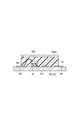
- the adhesive sheet 100 includes a film adhesive 10 on a base film 20.
- the adhesive sheet 100 can be obtained by removing the base film 20 in the step of obtaining the film adhesive 10.
- the adhesive sheet 110 further includes a cover film 30 on the surface of the adhesive sheet 100 opposite to the base film 20.
- cover film 30 include a PET film, a PE film, and an OPP film.
- the film adhesive 10 may be laminated on a dicing tape.
- the dicing / die bonding integrated adhesive sheet obtained in this way the lamination process to the semiconductor wafer can be performed at a time, and the work efficiency can be improved.
- the dicing tape examples include plastic films such as a polytetrafluoroethylene film, a polyethylene terephthalate film, a polyethylene film, a polypropylene film, a polymethylpentene film, and a polyimide film.
- the dicing tape may be subjected to surface treatment such as primer treatment, UV treatment, corona discharge treatment, polishing treatment, and etching treatment as necessary.
- the dicing tape is preferably adhesive.
- Examples of such a dicing tape include those obtained by imparting adhesiveness to the plastic film and those obtained by providing an adhesive layer on one side of the plastic film.
- Examples of such a dicing / die bonding integrated adhesive sheet include an adhesive sheet 120 shown in FIG. 4 and an adhesive sheet 130 shown in FIG.
- the adhesive sheet 120 uses a dicing tape 60 in which an adhesive layer 50 is provided on a base film 40 that can ensure elongation when a tensile tension is applied, as a supporting base material.
- the adhesive layer 50 has a structure in which the film adhesive 10 is provided.
- the adhesive sheet 130 has a structure in which a base film 20 is further provided on the surface of the film adhesive 10 in the adhesive sheet 120.
- the base film 40 examples include the plastic films described for the dicing tape.
- the pressure-sensitive adhesive layer 50 can be formed using, for example, a resin composition that includes a liquid component and a thermoplastic component and has an appropriate tack strength.
- a method of forming the pressure-sensitive adhesive layer 50 by applying the resin composition on the base film 40 and drying the pressure-sensitive adhesive layer 50 once formed on another film such as a PET film. The method of bonding with the base film 40 etc. are mentioned.
- a method of laminating the film adhesive 10 on the dicing tape 60 a method of directly applying and drying the varnish of the above adhesive composition on the dicing tape 60, a method of screen printing the varnish on the dicing tape 60, Examples thereof include a method in which the film adhesive 10 is prepared in advance and is laminated on the dicing tape 60 by pressing or hot roll laminating. Lamination by hot roll laminating is preferred because it can be continuously produced and is efficient.
- the thickness of the dicing tape 60 is not particularly limited, and can be appropriately determined based on the knowledge of those skilled in the art depending on the thickness of the film adhesive 10 and the application of the dicing / die bonding integrated adhesive sheet.
- the thickness of the dicing tape 60 is 60 ⁇ m or more, there is a tendency that it is easy to suppress deterioration in handleability, tearing due to the expand, and the like.
- the thickness of the dicing tape is 180 ⁇ m or less, it is easy to achieve both economy and good handling properties.
- FIG. 6 is a cross-sectional view showing the semiconductor device.
- the semiconductor device 200 is a semiconductor device in which a second semiconductor element Waa is stacked on a first semiconductor element Wa.
- the first semiconductor element Wa at the first stage is electrically connected to the substrate 14 via the first wire 88, and the first semiconductor element Wa is formed on the first semiconductor element Wa.
- the second semiconductor element Waa in the second stage larger than the area of the first wire 88 is pressure-bonded via the film adhesive 10 so that the first wire 88 and the first semiconductor element Wa are embedded in the film adhesive 10. This is a buried wire type semiconductor device.
- the substrate 14 and the second semiconductor element Waa are further electrically connected via the second wire 98, and the second semiconductor element Waa is sealed with the sealing material 42. ing.
- the thickness of the first semiconductor element Wa is 10 to 170 ⁇ m, and the thickness of the second semiconductor element Waa is 20 to 400 ⁇ m.
- the first semiconductor element Wa embedded in the film adhesive 10 is a controller chip for driving the semiconductor device 200.
- the substrate 14 is composed of an organic substrate 90 on which two circuit patterns 84 and 94 are formed on the surface.
- the first semiconductor element Wa is crimped onto the circuit pattern 94 via an adhesive 41
- the second semiconductor element Waa is a circuit pattern 94 in which the first semiconductor element Wa is not crimped.
- the semiconductor element Wa and a part of the circuit pattern 84 are pressure-bonded to the substrate 14 via the film adhesive 10. Unevenness caused by the circuit patterns 84 and 94 on the substrate 14 is embedded by the film adhesive 10.
- the second semiconductor element Waa, the circuit pattern 84, and the second wire 98 are sealed with a resin sealing material 42.
- a semiconductor device includes: a first die bonding step of electrically connecting a first semiconductor element on a substrate through a first wire; and a second semiconductor element having a larger area than the first semiconductor element.
- a second die-bonding step of embedding the first wire and the first semiconductor element in the film-like adhesive by pressing the film-like adhesive so as to cover the film.
- the manufacturing procedure of the semiconductor device 200 will be specifically described as an example.
- the first semiconductor element Waa with the adhesive 41 is pressure-bonded on the circuit pattern 94 on the substrate 14, and the circuit pattern 84 on the substrate 14 and the first pattern are connected to each other via the first wire 88.
- the first semiconductor element Wa is electrically connected (first die bonding step).
- the adhesive sheet 100 is laminated on one side of a semiconductor wafer (for example, 8-inch size), and the base film 20 is peeled off, so that the film adhesive 10 is attached to one side of the semiconductor wafer.
- the film adhesive is diced into a predetermined size (for example, 7.5 mm square), and the dicing tape 60 is peeled off, as shown in FIG.
- a second semiconductor element Waa to which 10 is attached is obtained (laminating step).
- the laminating step is preferably performed at 50 to 100 ° C., more preferably 60 to 80 ° C.
- the temperature in the laminating step is 50 ° C. or higher, good adhesion to the semiconductor wafer can be obtained.
- the temperature of the laminating process is 100 ° C. or lower, the film-like adhesive 10 can be prevented from flowing excessively during the laminating process, so that it is possible to prevent a change in thickness and the like.
- a dicing method As a dicing method, a blade dicing method using a rotary blade, a method of cutting the film adhesive 10 or both the wafer and the film adhesive 10 with a laser, and a general-purpose method such as stretching under normal temperature or cooling conditions Etc.
- the second semiconductor element Waa to which the film adhesive 10 is attached is pressure-bonded to the substrate 14 to which the first semiconductor element Wa is connected via the wire 88.
- the second semiconductor element Waa attached with the film adhesive 10 is placed so that the film adhesive 10 covers the first semiconductor element Wa
- the second semiconductor element Waa is fixed to the substrate 14 by pressing the second semiconductor element Waa to the substrate 14 (second die bonding step).
- the film adhesive 10 is preferably pressure-bonded for 0.5 to 3.0 seconds under conditions of 80 to 180 ° C. and 0.01 to 0.50 MPa.
- the substrate 14 and the second semiconductor element Waa are electrically connected via the second wire 98, the circuit pattern 84, the second wire 98, and the second semiconductor element are connected.
- the entire Waa is sealed with the sealing material 42 under the conditions of 170 to 180 ° C. and 5 to 8 MPa (sealing process).
- the semiconductor device 200 can be manufactured through such steps.
- the first semiconductor element is electrically connected to the substrate via the first wire, and the area of the first semiconductor element is larger than that of the first semiconductor element.
- the shear modulus at 150 ° C. used for pressure-bonding the second semiconductor element and embedding the first wire and the first semiconductor element is 1 Manufactured using a film adhesive that is 5 MPa or less.
- voids generated particularly in the second die bonding step can be eliminated by a sealing step which is a subsequent step. Thereby, a special process for eliminating the air gap is not required separately, and an increase in lead time can be suppressed.
- the substrate 14 is the organic substrate 90 having the circuit patterns 84 and 94 formed on the surface thereof at two locations.
- the substrate 14 is not limited to this, and a metal substrate such as a lead frame is used. Also good.
- the semiconductor device 200 has a configuration in which the second semiconductor element Waa is stacked on the first semiconductor element Wa and the semiconductor elements are stacked in two stages, the configuration of the semiconductor device is not limited thereto. I can't.
- a third semiconductor element may be further stacked on the second semiconductor element Waa, or a plurality of semiconductor elements may be further stacked on the second semiconductor element Waa. As the number of stacked semiconductor elements increases, the capacity of the obtained semiconductor device can be increased.
- the adhesive sheet 100 shown in FIG. 2 is laminated on one side of the semiconductor wafer, and the base film 20 is peeled off, so that the film adhesive 10 is applied.
- the adhesive sheet used at the time of lamination is not limited to this.
- dicing / die bonding integrated adhesive sheets 120 and 130 shown in FIGS. 4 and 5 can be used. In this case, it is not necessary to attach the dicing tape 60 separately when dicing the semiconductor wafer.
- a semiconductor element obtained by dividing a semiconductor wafer instead of a semiconductor wafer may be laminated on the adhesive sheet 100.
- the dicing process can be omitted.
- Examples 1 and 2 and Comparative Examples 1 to 3 According to Table 1 (unit: part by mass), the epoxy resin and phenol resin, which are thermosetting resins, and the inorganic filler were weighed to obtain a composition, and further cyclohexanone was added and mixed with stirring. Acrylic rubber, which is a thermoplastic resin, was added thereto and stirred, and then a coupling agent and a curing accelerator were further added and stirred until each component became uniform to obtain a varnish.
- the product name of each component in Table 1 means the following.
- HE100C-30 (trade name, manufactured by Air Water Co., Ltd., phenol resin: hydroxyl group equivalent 175, softening point 79 ° C., water absorption 1 mass%, heating mass reduction rate 4 mass%)
- HE200C-10 (trade name, manufactured by Air Water Co., Ltd., phenol resin: hydroxyl group equivalent 200, softening point 65 to 76 ° C., water absorption 1% by mass, heating mass decrease rate 4% by mass)
- HE910-10 (trade name, manufactured by Air Water Co., Ltd., phenol resin: hydroxyl group equivalent 101, softening point 83 ° C., water absorption 1 mass%, heating mass reduction rate 3 mass%).
- HTR-860P-3CSP (sample name: manufactured by Nagase ChemteX Corporation, acrylic rubber: weight average molecular weight 800,000, glycidyl functional group monomer ratio 3 mol%, Tg 12 ° C.)
- HTR-860P-30B-CHN (Sample name, manufactured by Nagase ChemteX Corporation, acrylic rubber: weight average molecular weight 230,000, glycidyl functional group monomer ratio 8 mol%, Tg-7 ° C)
- Cureazole 2PZ-CN (trade name, manufactured by Shikoku Kasei Kogyo Co., Ltd., 1-cyanoethyl-2-phenylimidazole)
- the obtained varnish was filtered through a 100 mesh filter and vacuum degassed.
- the varnish after vacuum defoaming was applied onto a polyethylene terephthalate (PET) film (thickness: 38 ⁇ m) which was a base film and was subjected to a release treatment.
- PET polyethylene terephthalate
- the applied varnish was heat-dried in two stages of 90 ° C. for 5 minutes, followed by 140 ° C. for 5 minutes.
- an adhesive sheet provided with a film adhesive having a thickness of 60 ⁇ m in a B-stage state on a PET film was obtained.
- the base film was peeled and removed from the film adhesive and punched out to 10 mm square in the thickness direction.
- a sample for evaluation of a film adhesive having a size of 10 mm square and a thickness of 360 ⁇ m was obtained by preparing and bonding a plurality of these.
- a circular aluminum plate jig having a diameter of 8 mm was set in a dynamic viscoelastic device ARES (manufactured by TA Instruments Japan Co., Ltd.), and the evaluation sample was sandwiched between the jigs. Thereafter, while giving 5% strain to the sample for evaluation at a frequency of 1 Hz, the temperature was raised from room temperature (30 ° C.) to 125 ° C.
- shear viscosity measurement In the same manner as the shear modulus measurement, the shear viscosity was increased while raising the temperature from room temperature (30 ° C.) to 140 ° C. at a rate of 5 ° C./min while giving 5% strain to the evaluation sample at a frequency of 1 Hz. It was measured. And the measured value in 80 degreeC was recorded.
- the film adhesive was cut into a width of 4 mm and a length of 30 mm. This was heated at 120 ° C. for 2 hours and 170 ° C. for 3 hours to obtain a sample for evaluation in which the film adhesive was cured. Thereafter, the evaluation sample is set in a dynamic viscoelastic device (product name: Rheogel-E4000, manufactured by UMB Co., Ltd.), a tensile load is applied, and a tensile elastic modulus is applied at a frequency of 10 Hz and a heating rate of 3 ° C./min. Was measured. The measured values at 170 to 190 ° C. were recorded.
- a dynamic viscoelastic device product name: Rheogel-E4000, manufactured by UMB Co., Ltd.
- the chip with integrated film is pressure-bonded to an evaluation substrate having a maximum surface roughness of 6 ⁇ m under the conditions of 120 ° C., 0.20 MPa, 2 seconds, and then heated at 120 ° C. for 2 hours to semi-cure the integrated film. It was. Thereby, a substrate with a chip was obtained.
- a semiconductor element with an adhesive sheet was pressure-bonded to the obtained substrate with chip under the conditions of 120 ° C., 0.20 MPa, and 2 seconds. At this time, alignment was performed so that the chip that was previously crimped was in the middle of the semiconductor element with the adhesive sheet.
- the obtained structure was heated at 125 ° C. for 1 hour and at 150 ° C. for 45 minutes in the same manner as the shear modulus measurement.
- the structure which was naturally cooled to room temperature after heating was analyzed with an ultrasonic C-SCAN diagnostic imaging apparatus (Insight Co., Ltd., product number IS350, probe: 75 MHz), and the embedding property was confirmed after press bonding.
- the embedding after crimping was evaluated according to the following criteria. ⁇ : The ratio of the void area to the pressure-bonded film area is less than 10%. X: The ratio of the void area to the pressure-bonded film area is 10% or more.
- a structure was prepared in the same manner as the evaluation of embedding after pressure bonding. This structure was heated at 170 ° C. for 3 hours to cure the film adhesive, and then the height difference in the diagonal direction of the semiconductor element was measured by a surface roughness meter for 8 mm. The difference between the maximum value and the minimum value of the measured values obtained was recorded as the amount of warpage of the structure.
Landscapes
- Chemical & Material Sciences (AREA)
- Organic Chemistry (AREA)
- Inorganic Chemistry (AREA)
- Adhesives Or Adhesive Processes (AREA)
- Adhesive Tapes (AREA)
- Die Bonding (AREA)
- Structures Or Materials For Encapsulating Or Coating Semiconductor Devices Or Solid State Devices (AREA)
Abstract
本発明は、基板上に第1のワイヤを介して第1の半導体素子を電気的に接続する第1のダイボンド工程と、第1の半導体素子の面積よりも大きい第2の半導体素子の片面に、150℃におけるずり弾性率が1.5MPa以下であるフィルム状接着剤を貼付するラミネート工程と、フィルム状接着剤が貼付された第2の半導体素子を、フィルム状接着剤が第1の半導体素子を覆うように載置し、フィルム状接着剤を圧着することで、第1のワイヤ及び第1の半導体素子をフィルム状接着剤に埋め込む第2のダイボンド工程と、を備える、半導体装置の製造方法に関する。
Description
本発明は半導体装置の製造方法、及びフィルム状接着剤に関する。
半導体装置における基板の配線、半導体チップに付設されたワイヤ等による凹凸を充填可能な、ワイヤ埋込型の半導体装置を得ることができる接着シートが知られている(例えば、特許文献1及び2)。当該接着シートは、凹凸充填時において高い流動性を発現するべく、熱硬化性成分を主成分として含有している。
近年、このようなワイヤ埋込型の半導体装置の動作の高速化が重要視されている。従来は積層された半導体素子の最上段に、半導体装置の動作を制御するコントローラチップが配置されていたが、動作の高速化を実現するため、最下段にコントローラチップを配置した半導体装置のパッケージ技術が開発されている。このようなパッケージの1つの形態として、多段に積層した半導体素子のうち、2段目の半導体素子を圧着する際に使用するフィルム状接着剤を分厚くし、当該フィルム状接着剤内部にコントローラチップを埋め込むパッケージが注目を集めている。このような用途に使用されるフィルム状接着剤には、コントローラチップ、コントローラチップに接続されているワイヤ、基板表面の凹凸起因の段差等を埋め込むことのできる高い流動性が必要となる。
しかしながら、特許文献1及び2に記載の接着シートのように、単に硬化前の流動性が高いことを特徴とする接着シートを用いると、半導体素子の薄型化に伴い、硬化後に半導体装置全体が反り易いという問題がある。また、当該接着シートを用いた圧着時に空隙が発生した場合、それを従来の工程内で除去することが難しいという問題がある。このため、得られる半導体装置の接続信頼性の確保のためには、さらなる検討が必要であるというのが現状である。なお、特に後者における空隙の除去については、加圧オーブン等により加熱及び加圧する工程を別途設けることにより一応可能である。しかしながら、工程数の増加により、汎用品種に比べてリードタイムが増大してしまう。
そこで、本発明は、リードタイムの増大を抑制しつつ、接続信頼性に優れる半導体装置を得ることが可能な、半導体装置の製造方法を提供することを目的とする。本発明はまた、当該製造方法に用いられるフィルム状接着剤を提供することを目的とする。
本発明は、基板上に第1のワイヤを介して第1の半導体素子を電気的に接続する第1のダイボンド工程と、第1の半導体素子の面積よりも大きい第2の半導体素子の片面に、150℃におけるずり弾性率が1.5MPa以下であるフィルム状接着剤を貼付するラミネート工程と、フィルム状接着剤が貼付された第2の半導体素子を、フィルム状接着剤が第1の半導体素子を覆うように載置し、フィルム状接着剤を圧着することで、第1のワイヤ及び第1の半導体素子をフィルム状接着剤に埋め込む第2のダイボンド工程と、を備える、半導体装置の製造方法を提供する。
本発明によれば、リードタイムの増大を抑制しつつ、接続信頼性に優れる半導体装置を得ることが可能である。より具体的には、150℃におけるずり弾性率が1.5MPa以下であるフィルム状接着剤を用いることで、特に第2のダイボンド工程において生じる空隙(ボイド)を、後工程である封止工程により解消することができる。これにより、空隙を解消するための特別なプロセスが別途必要とされず、リードタイムが増大しない。
本発明において、150℃におけるずり弾性率とは、フィルム状接着剤に5%の歪みを周波数1Hzで与えながら、5℃/分の昇温速度で室温から125℃まで昇温して1時間保持した後、5℃/分の昇温速度でさらに150℃まで昇温して45分間保持した後、動的粘弾性測定装置を用いて測定することで得られるものである。
本発明において、フィルム状接着剤の、硬化後の170~190℃における引張弾性率が15MPa以下であることが好ましい。フィルム状接着剤が、硬化後において低弾性であることにより、封止工程時に良好な埋め込み性と応力緩和性とを得ることが可能となる。例えば薄型の第2の半導体素子を使用した場合でも、フィルム状接着剤が硬化した後の半導体装置の反りを抑制することができる。これにより、半導体装置の応力が緩和され、良好な接続信頼性を示す半導体装置を得易くなる。
本発明において、フィルム状接着剤の、80℃におけるずり粘度が15000Pa・s以下であることが好ましい。これにより、良好な埋め込み性を得易くなる。
本発明において、フィルム状接着剤が、アクリル樹脂及びエポキシ樹脂を含むことが好ましい。熱可塑性成分と熱硬化成分とを併用することにより、良好な埋め込み性、熱硬化性及び応力緩和性を得易くなる。
本発明において、アクリル樹脂が、重量平均分子量が10万~50万である第1のアクリル樹脂と、重量平均分子量が60万~100万である第2のアクリル樹脂とを含み、アクリル樹脂の全質量を基準として、第1のアクリル樹脂の含有量が50質量%以上であることが好ましい。このように分子量分布の幅を広げることにより、応力緩和性が向上し、硬化後の基板の反りを低減し易くなる。また、成膜性及び接着性を維持したまま、埋め込み性を向上し易くなる。
本発明において、フィルム状接着剤が、無機フィラー及び有機フィラーの少なくとも一方を含むことが好ましい。これにより、フィルム状接着剤の取り扱い性等がより向上すると共に、より良好なずり弾性率、接着力等の機械特性を得ることができる。
本発明は、また、基板上に第1のワイヤを介して第1の半導体素子が電気的に接続されると共に、第1の半導体素子上に、第1の半導体素子の面積よりも大きい第2の半導体素子が圧着されてなる半導体装置において、第2の半導体素子を圧着すると共に、第1のワイヤ及び第1の半導体素子を埋め込むために用いられる、150℃におけるずり弾性率が1.5MPa以下である、フィルム状接着剤を提供する。本発明のフィルム状接着剤を用いることで、リードタイムの増大を抑制しつつ、接続信頼性に優れる半導体装置を得ることが可能である。
本発明のフィルム状接着剤において、硬化後の170~190℃における引張弾性率が15MPa以下であることが好ましい。
本発明のフィルム状接着剤において、80℃におけるずり粘度が15000Pa・s以下であることが好ましい。
本発明のフィルム状接着剤は、アクリル樹脂及びエポキシ樹脂を含むことが好ましい。
本発明のフィルム状接着剤において、アクリル樹脂が、重量平均分子量が10万~50万である第1のアクリル樹脂と、重量平均分子量が60万~100万である第2のアクリル樹脂とを含み、アクリル樹脂の全質量を基準として、第1のアクリル樹脂の含有量が50質量%以上であることが好ましい。
本発明のフィルム状接着剤は、無機フィラー及び有機フィラーの少なくとも一方を含むことが好ましい。
本発明によれば、リードタイムの増大を抑制しつつ、接続信頼性に優れる半導体装置を得ることが可能な、半導体装置の製造方法を提供することができる。また、本発明によれば、当該製造方法に用いられるフィルム状接着剤を提供することができる。
以下、図面を参照しながら本発明の好適な実施形態について詳細に説明する。以下の説明では、同一又は相当部分には同一符号を付し、重複する説明は省略する。また、上下左右等の位置関係は、特に断らない限り、図面に示す位置関係に基づくものとする。さらに、図面の寸法比率は図示の比率に限られるものではない。なお、本明細書における「(メタ)アクリル」とは、「アクリル」及びそれに対応する「メタクリル」を意味する。
(フィルム状接着剤)
図1は、本実施形態に係るフィルム状接着剤10を模式的に示す断面図である。フィルム状接着剤10は、熱硬化性であり、半硬化(Bステージ)状態を経て、硬化処理後に完全硬化物(Cステージ)状態となり得る接着剤組成物をフィルム状に成形してなるものである。
図1は、本実施形態に係るフィルム状接着剤10を模式的に示す断面図である。フィルム状接着剤10は、熱硬化性であり、半硬化(Bステージ)状態を経て、硬化処理後に完全硬化物(Cステージ)状態となり得る接着剤組成物をフィルム状に成形してなるものである。
フィルム状接着剤10は、150℃におけるずり弾性率が1.5MPa以下である。リードタイムの増大を抑制しつつ、接続信頼性に優れる半導体装置をより得易くなるという観点から、ずり弾性率は1.2MPa以下であることが好ましく、1.0MPa以下であることがより好ましく、0.8MPa以下であることがさらに好ましい。ずり弾性率の下限は特に限定されないが、過度な流動性を抑制するという観点から0.01MPaとすることができる。なお、ずり弾性率は、後述のとおり(a)~(f)成分の種類及び量を調整することにより、調整することが可能である。例えば、150℃におけるずり弾性率を下げる(1.5MPa以下にする)ための指針としては、(a1)成分の量を増やすこと、(a2)成分の量を減らすこと、(b)成分の重量平均分子量を下げること、(c)成分の量を減らすこと、(d)成分の量を減らすこと、(e)成分の量を減らすこと、などが挙げられるが、この限りではない。
フィルム状接着剤10は、硬化後の170~190℃における引張弾性率が15MPa以下であることが好ましい。良好な埋め込み性と応力緩和性とをより得易くなるという観点から、引張弾性率は12MPa以下であることがより好ましく、10MPa以下であることがさらに好ましく、8MPa以下であることが特に好ましい。引張弾性率の下限は特に限定されないが、適度な接着性を確保するという観点から1MPaとすることができる。引張弾性率は、例えば周波数10Hzとして、動的粘弾性測定装置を用いて測定することができる。
フィルム状接着剤10は、80℃におけるずり粘度が15000Pa・s以下であることが好ましい。良好な埋め込み性を得易くなるという観点から、ずり粘度は10000Pa・s以下であることがより好ましく、9000Pa・s以下であることがさらに好ましい。ずり粘度の下限は特に限定されないが、過度な流動性を抑制するという観点から1000Pa・sとすることができる。ずり粘度は、例えば動的粘弾性測定装置を用いて測定することができる。
フィルム状接着剤10の含有成分は特に限定されないが、例えば、(a)熱硬化性成分、(b)熱可塑性成分、(c)無機フィラー、(d)有機フィラー、(e)硬化促進剤、(f)その他の成分、等を含むことができる。これら(a)~(f)成分の種類及び量を調整することにより、フィルム状接着剤10の特性を調整することができる。
(a)熱硬化性成分
熱硬化性成分としては熱硬化性樹脂が挙げられる。特に、半導体素子を実装する場合に要求される耐熱性及び耐湿性の観点から、熱硬化性成分としてエポキシ樹脂、フェノール樹脂等が好ましい。
熱硬化性成分としては熱硬化性樹脂が挙げられる。特に、半導体素子を実装する場合に要求される耐熱性及び耐湿性の観点から、熱硬化性成分としてエポキシ樹脂、フェノール樹脂等が好ましい。
例えばエポキシ樹脂としては、芳香環含有エポキシ樹脂、複素環含有エポキシ樹脂、脂環式エポキシ樹脂等の、一般に知られているエポキシ樹脂を用いることができる。また、エポキシ樹脂は多官能エポキシ樹脂であってもよい。エポキシ樹脂としては、具体的には、例えば、ビスフェノールA型エポキシ樹脂、ビスフェノールF型エポキシ樹脂、ビスフェノールE型エポキシ樹脂、これらのビスフェノール型エポキシ樹脂を変性させた二官能エポキシ樹脂、クレゾールノボラック型エポキシ樹脂、ビスフェノールAノボラック型エポキシ樹脂、フルオレン変性エポキシ樹脂、トリフェニルメタン型エポキシ樹脂、ビフェニル型エポキシ樹脂、グリシジルアミン型エポキシ樹脂、ナフタレン変性エポキシ樹脂等を用いることができる。
エポキシ樹脂としては、例えば、新日化エポキシ製造株式会社製のYDFシリーズ及びYDCNシリーズ、株式会社プリンテック製のEPOX-MKシリーズ及びVG-3101L等が挙げられる。
また、フェノール樹脂としては、例えば、ノボラック型フェノール樹脂、ザイロック型フェノール樹脂、ビフェニル型フェノール樹脂、トリフェニルメタン型フェノール樹脂、フェノール環上の水素をアリール基で置換した変性フェノール樹脂等が挙げられる。なお、フェノール樹脂としては、耐熱性の観点から、85℃、85%RHの恒温恒湿槽に48時間投入後の吸水率が2質量%以下で、熱重量分析計(TGA)で測定した350℃での加熱質量減少率(昇温速度:5℃/min、雰囲気:窒素)が5質量%未満のものが好ましい。
フェノール樹脂としては、例えば、DIC株式会社製のフェノライトKA及びTDシリーズ、エア・ウォーター株式会社製のHEシリーズ等が挙げられる。
(a)熱硬化性成分としてエポキシ樹脂及びフェノール樹脂を併用する場合、エポキシ樹脂及びフェノール樹脂の配合比は、それぞれエポキシ当量と水酸基当量の当量比で0.70/0.30~0.30/0.70となるのが好ましく、0.65/0.35~0.35/0.65となるのがより好ましく、0.60/0.40~0.40/0.60となるのがさらに好ましく、0.60/0.40~0.50/0.50となるのが特に好ましい。配合比が上記範囲内であることで、優れた硬化性、流動性等を有するフィルム状接着剤10が得易くなる。
なお、硬化後における半導体装置の反りを抑制するという観点から、硬化速度の異なる熱硬化性樹脂を組み合わせることが好ましい。具体的には、上記に例示したエポキシ樹脂及びフェノール樹脂のうち、例えば(a1)軟化点が60℃以下又は常温で液体であるもの(硬化して接着作用を有するものであれば特に限定されない)と、(a2)軟化点が60℃超(常温で固体)であるものと、を組み合わせて用いることが好ましい。なお、ここでいう常温とは5~35℃を意味する。
(a1)成分の含有量は、(a)成分の全質量を基準として10~50質量%であることが好ましく、20~40質量%であることがより好ましい。これにより、埋め込み性と、ダイシング、ピックアップ等のプロセス適性とを両立し易くなる。
(a2)成分の含有量は、(a)成分の全質量を基準として10質量%以上であることが好ましく、15質量%以上であることがより好ましい。これにより、製膜性、流動性、応力緩和性等を調整し易くなる。なお、(a2)成分の含有量の上限は特に限定されないが、(a)成分の全質量を基準として90質量%とすることができる。
(b)熱可塑性成分
(b)熱可塑性成分としては、架橋性官能基を有するモノマー比率が高く分子量が低い熱可塑性成分と、架橋性官能基を有するモノマー比率が低く分子量が高い熱可塑性成分との併用が好ましい。例えば、(b)成分は、(b1)架橋性官能基を有するモノマー単位をモノマー単位全量に対し5~15モル%有し、重量平均分子量が10万~50万でありガラス転移温度Tgが-50~50℃である熱可塑性成分と、(b2)架橋性官能基を有するモノマー単位をモノマー単位全量に対し比率で1~7モル%有し、重量平均分子量が60万~100万でありガラス転移温度Tgが-50~50℃である熱可塑性成分とを含むことが好ましい。
(b)熱可塑性成分としては、架橋性官能基を有するモノマー比率が高く分子量が低い熱可塑性成分と、架橋性官能基を有するモノマー比率が低く分子量が高い熱可塑性成分との併用が好ましい。例えば、(b)成分は、(b1)架橋性官能基を有するモノマー単位をモノマー単位全量に対し5~15モル%有し、重量平均分子量が10万~50万でありガラス転移温度Tgが-50~50℃である熱可塑性成分と、(b2)架橋性官能基を有するモノマー単位をモノマー単位全量に対し比率で1~7モル%有し、重量平均分子量が60万~100万でありガラス転移温度Tgが-50~50℃である熱可塑性成分とを含むことが好ましい。
(b)成分としては、熱可塑性樹脂であるアクリル樹脂(アクリル系樹脂)が好ましく、さらに、ガラス転移温度Tgが-50℃~50℃であり、グリシジルアクリレート、グリシジルメタクリレート等のエポキシ基又はグリシジル基を架橋性官能基として有する官能性モノマーを重合して得られる、エポキシ基含有(メタ)アクリル共重合体等のアクリル樹脂がより好ましい。
このようなアクリル樹脂として、エポキシ基含有(メタ)アクリル酸エステル共重合体、エポキシ基含有アクリルゴム等を使用することができ、エポキシ基含有アクリルゴムがより好ましい。エポキシ基含有アクリルゴムは、アクリル酸エステルを主成分とし、主として、ブチルアクリレートとアクリロニトリル等の共重合体、エチルアクリレートとアクリロニトリル等の共重合体等からなる、エポキシ基を有しているアクリルゴムである。
なお、(b)成分の架橋性官能基としては、エポキシ基の他、アルコール性又はフェノール性水酸基、カルボキシル基等の架橋性官能基が挙げられる。
(b1)成分において、高い接着力が発現し易く、また150℃におけるずり弾性率を低くし易い観点から、架橋性官能基を有するモノマー単位はモノマー単位全量に対し5~15モル%であることが好ましく、5~10モル%がより好ましい。
(b2)成分において、硬化後における弾性率の過度な上昇を抑制し易いという観点から、架橋性官能基を有するモノマー単位はモノマー単位全量に対し1~7モル%であることが好ましく、2~5モル%がより好ましい。
(b1)成分(第1のアクリル樹脂)の重量平均分子量は、10万~50万であることが好ましい。(b1)成分の重量平均分子量が10万以上であると、フィルム成膜性がより良好になると共に、フィルム状接着剤10の接着強度と耐熱性をより高めることができる。(b1)成分の重量平均分子量が50万以下であると、ずり粘度を低減し易くなるため、フィルム状接着剤10の埋込性がより良好になる。
(b2)成分(第2のアクリル樹脂)の重量平均分子量は、60万~100万であることが好ましい。(b2)成分の重量平均分子量が60万以上であると、(b1)成分との併用により成膜性を向上させる効果が一段と良好になる。(b2)成分の重量平均分子量が100万以下であると、未硬化状態のフィルム状接着剤10のずり粘度を低減し易くなるため、埋込性がより良好になる。また、未硬化状態のフィルム状接着剤10の切削性が改善し、ダイシングの品質がより良好になる場合がある。
重量平均分子量は、ゲルパーミエーションクロマトグラフィー法(GPC)により、標準ポリスチレンによる検量線を用いて得られるポリスチレン換算値である。
また、(b1)成分及び(b2)成分のガラス転移温度Tgは-50~50℃であることが好ましい。ガラス転移温度Tgが50℃以下であると、フィルム状接着剤10の柔軟性がより良好になる。一方、ガラス転移温度Tgが-50℃以上であると、フィルム状接着剤10の柔軟性が高くなり過ぎないため、半導体ウェハをダイシングする際にフィルム状接着剤10を切断し易い。このため、バリの発生によりダイシング性が悪化することを抑制し易い。
(b)成分全体のガラス転移温度Tgは-20℃~40℃であることが好ましく、-10℃~30℃であることが好ましい。これにより、ダイシング時にフィルム状接着剤10が切断し易くなるため樹脂くずが発生し難く、フィルム状接着剤10の接着力と耐熱性とを高くし易く、また未硬化状態のフィルム状接着剤10の高い流動性を発現し易くなる。
ガラス転移温度Tgは、熱示差走査熱量計(例えば、株式会社リガク製「Thermo Plus 2」)を用いて測定することができる。
(b)成分は、市販品として入手することも可能である。例えば、(b1)成分としては、アクリルゴムHTR-860P-30B-CHN(商品名、ナガセケムテックス株式会社製)等が挙げられる。この化合物は、架橋性の部位としてグリシジル部位を有し、アクリル酸誘導体からなるアクリルゴムをベース樹脂とする化合物であり、重量平均分子量が23万、ガラス転移温度Tgが-7℃である。また、(b2)成分としては、アクリルゴムHTR-860P-3CSP(商品名、ナガセケムテックス株式会社製)等が挙げられる。
(b1)成分(第1のアクリル樹脂)の含有量は、(b)成分(アクリル樹脂)の全質量を基準として50質量%以上であることが好ましく、70質量%以上であることがより好ましい。これにより、良好な埋め込み性、応力緩和性、製膜性、接着性等を得易くなる。なお、(b1)成分の含有量の上限は特に限定されないが、(b)成分の全質量を基準として90質量%とすることができる。
(b2)成分の含有量は、(b)成分の全質量を基準として10質量%以上であることが好ましく、30質量%以上であることがより好ましい。これにより、製膜性、接着性、弾性率等を調整し易くなる。なお、(b2)成分の含有量の上限は特に限定されないが、(b)成分の全質量を基準として50質量%とすることができる。
(b)成分の含有量は、(a)成分を100質量部としたとき、20~160質量部であることが好ましく、50~120質量部であることがより好ましい。(b)成分の含有量が上記下限値以上であることにより、良好な製膜性、埋め込み性、接着性、応力緩和性等が得易い。一方、(b)成分の含有量が上記上限値以下であることにより、良好な製膜性、埋め込み性等を得易くなる。
(c)無機フィラー
(c)成分としては、Bステージ状態におけるフィルム状接着剤10のダイシング性の向上、フィルム状接着剤10の取扱い性の向上、熱伝導性の向上、ずり粘度(溶融粘度)の調整、チクソトロピック性の付与、接着力の向上等の観点から、シリカフィラー等が好ましい。
(c)成分としては、Bステージ状態におけるフィルム状接着剤10のダイシング性の向上、フィルム状接着剤10の取扱い性の向上、熱伝導性の向上、ずり粘度(溶融粘度)の調整、チクソトロピック性の付与、接着力の向上等の観点から、シリカフィラー等が好ましい。
(c)成分は、未硬化状態のフィルム状接着剤10のダイシング性を向上し、硬化後の接着力を十分に発現させる目的で、平均粒径の異なる2種類以上のフィラーを含むことが好ましい。(c)成分は、例えば(c1)未硬化状態のフィルム状接着剤10のダイシング性向上を目的とした平均粒径が0.2μm以上の第1のフィラーと、(c2)硬化後の接着力を十分に発現させることを目的とした平均粒径が0.2μm未満の第2のフィラーを含むことが好ましい。
平均粒径は、レーザー回折式粒度分布測定装置を用いて、アセトンを溶媒として分析した場合に得られる値とする。第1及び第2のフィラーの平均粒径は、粒度分布測定装置で分析した場合に、それぞれのフィラーが含まれていることが判別できる程度に、その差が大きいことがより好ましい。
(c1)成分の含有量は、(c)成分の全質量を基準として30質量%以上であることが好ましい。(c1)成分の含有量が30質量%以上であることにより、フィルムの破断性の悪化、未硬化状態のフィルム状接着剤10の流動性の悪化を抑制し易くなる。なお、(c1)成分の含有量の上限は特に限定されないが、(c)成分の全質量を基準として95質量%とすることができる。
(c2)成分の含有量は、(c)成分の全質量を基準として5質量%以上であることが好ましい。(c2)成分の含有量が5質量%以上であることにより、硬化後の接着力を向上させ易い。なお、(c2)成分の含有量の上限は、適度な流動性を確保する観点から、(c)成分の全質量を基準として30質量%とすることができる。
(c)成分の含有量は、(a)成分を100質量部としたとき、10~90質量部であることが好ましい。(c)成分の含有量が上記下限値以上であることにより、未硬化状態のフィルム状接着剤10のダイシング性の悪化、硬化後の接着力の低下を抑制し易いという傾向がある。一方、(c)成分の含有量が上記上限値以下であることにより、未硬化状態のフィルム状接着剤10の流動性の低下、硬化後の弾性率の上昇を抑制し易いという傾向がある。
(d)有機フィラー
(d)成分としては、フィルム状接着剤10のダイシング性の向上、フィルム状接着剤10の取扱い性の向上、ずり粘度(溶融粘度)の調整、接着力の向上、硬化後の応力緩和性等の観点から、スチレン-PMMA変性ゴムフィラー、シリコーン変性ゴムフィラー等が好ましい。(d)成分の平均粒径は、硬化後の接着力を十分に発現し易くする観点から0.2μm以下であることが好ましい。
(d)成分としては、フィルム状接着剤10のダイシング性の向上、フィルム状接着剤10の取扱い性の向上、ずり粘度(溶融粘度)の調整、接着力の向上、硬化後の応力緩和性等の観点から、スチレン-PMMA変性ゴムフィラー、シリコーン変性ゴムフィラー等が好ましい。(d)成分の平均粒径は、硬化後の接着力を十分に発現し易くする観点から0.2μm以下であることが好ましい。
(d)成分の含有量は、(c)成分を100質量部としたとき、0~50質量部であることが好ましい。
(e)硬化促進剤
良好な硬化性を得る目的で、(e)硬化促進剤を用いることが好ましい。(e)成分としては、反応性の観点からイミダゾール系の化合物が好ましい。なお、(e)成分の反応性が高すぎると、フィルム状接着剤10の製造工程中の加熱によりずり粘度が上昇し易くなるだけではなく、経時による劣化を引き起こし易い傾向がある。一方、(e)成分の反応性が低すぎると、フィルム状接着剤10の硬化性が低下し易い傾向がある。フィルム状接着剤10が十分硬化されないまま製品内に搭載されると、十分な接着性が得られず、半導体装置の接続信頼性を悪化させる可能性がある。
良好な硬化性を得る目的で、(e)硬化促進剤を用いることが好ましい。(e)成分としては、反応性の観点からイミダゾール系の化合物が好ましい。なお、(e)成分の反応性が高すぎると、フィルム状接着剤10の製造工程中の加熱によりずり粘度が上昇し易くなるだけではなく、経時による劣化を引き起こし易い傾向がある。一方、(e)成分の反応性が低すぎると、フィルム状接着剤10の硬化性が低下し易い傾向がある。フィルム状接着剤10が十分硬化されないまま製品内に搭載されると、十分な接着性が得られず、半導体装置の接続信頼性を悪化させる可能性がある。
(e)成分を含有させることで、フィルム状接着剤10の硬化性がより向上する。一方、(e)成分の含有量が多すぎる場合には、フィルム状接着剤10の製造工程中の加熱によりずり粘度が上昇し易くなるだけではなく、経時による劣化を引き起こし易い傾向がある。このような観点から、(e)成分の含有量は、(a)成分を100質量部としたとき、0~0.20質量部であることが好ましい。
(f)その他の成分
上記成分以外に、接着性向上の観点から、本技術分野において使用され得るその他の成分をさらに適量用いてもよい。そのような成分としては、例えばカップリング剤が挙げられる。カップリング剤としては、γ-ウレイドプロピルトリエトキシシラン、γ-メルカプトプロピルトリメトキシシラン、3-フェニルアミノプロピルトリメトキシシラン、3-(2-アミノエチル)アミノプロピルトリメトキシシラン等が挙げられる。
上記成分以外に、接着性向上の観点から、本技術分野において使用され得るその他の成分をさらに適量用いてもよい。そのような成分としては、例えばカップリング剤が挙げられる。カップリング剤としては、γ-ウレイドプロピルトリエトキシシラン、γ-メルカプトプロピルトリメトキシシラン、3-フェニルアミノプロピルトリメトキシシラン、3-(2-アミノエチル)アミノプロピルトリメトキシシラン等が挙げられる。
(フィルム状接着剤)
フィルム状接着剤10は、例えば上記成分を含む接着剤組成物のワニスを基材フィルム上に塗布することによりワニスの層を形成する工程、加熱乾燥によりワニスの層から溶媒を除去する工程、基材フィルムを除去する工程、により得ることができる。
フィルム状接着剤10は、例えば上記成分を含む接着剤組成物のワニスを基材フィルム上に塗布することによりワニスの層を形成する工程、加熱乾燥によりワニスの層から溶媒を除去する工程、基材フィルムを除去する工程、により得ることができる。
ワニスは、上記成分を含む接着剤組成物を有機溶媒中で混合、混練等して調製することができる。混合及び混練は、通常の攪拌機、らいかい機、三本ロール、ボールミル等の分散機を用いることができる。これらの機器は適宜組み合わせて用いることができる。ワニスの塗布は、例えば、コンマコーター、ダイコータ―等により行うことができる。ワニスの加熱乾燥条件は、使用した有機溶媒が充分に揮散する条件であれば特に制限はなく、例えば60~200℃で0.1~90分間とすることができる。
有機溶媒としては、上記成分を均一に溶解、混練又は分散できるものであれば制限はなく、従来公知のものを使用することができる。このような溶媒としては、例えば、アセトン、メチルエチルケトン、メチルイソブチルケトン、シクロヘキサノン等のケトン系溶媒、ジメチルホルムアミド、ジメチルアセトアミド、Nメチルピロリドン、トルエン、キシレン等が挙げられる。乾燥速度が速く、価格が安い点でメチルエチルケトン、シクロヘキサノン等を使用することが好ましい。
上記基材フィルムとしては、特に制限はなく、例えば、ポリエステルフィルム(ポリエチレンテレフタレートフィルム等)、ポリプロピレンフィルム(OPP(Oriented PolyPropylene)フィルム等)、ポリイミドフィルム、ポリエーテルイミドフィルム、ポリエーテルナフタレートフィルム、メチルペンテンフィルム等が挙げられる。
フィルム状接着剤10の厚さは、第1のワイヤ及び第1の半導体素子、並びに基板の配線回路等の凹凸を十分に埋め込めるよう、20~200μmであることが好ましい。また、厚さが20μm以上であることで十分な接着力を得易くなり、200μm以下であることで半導体装置の小型化の要求に応え易くなる。このような観点から、フィルム状接着剤10の厚さは30~200μmであることがより好ましく、40~150μmであることがさらに好ましい。
厚いフィルム状接着剤10を得る方法としては、フィルム状接着剤10同士を貼り合わせる方法が挙げられる。
(接着シート)
接着シート100は、図2に示すように、基材フィルム20上にフィルム状接着剤10を備えるものである。接着シート100は、フィルム状接着剤10を得る工程において、基材フィルム20を除去しないことで得ることができる。
接着シート100は、図2に示すように、基材フィルム20上にフィルム状接着剤10を備えるものである。接着シート100は、フィルム状接着剤10を得る工程において、基材フィルム20を除去しないことで得ることができる。
接着シート110は、図3に示すように、接着シート100の基材フィルム20とは反対側の面にさらにカバーフィルム30を備えるものである。カバーフィルム30としては、例えば、PETフィルム、PEフィルム、OPPフィルム等が挙げられる。
フィルム状接着剤10は、ダイシングテープ上に積層されてもよい。これにより得られるダイシング・ダイボンディング一体型接着シートを用いることで、半導体ウェハへのラミネート工程を一度に行うことができ、作業の効率化が可能である。
ダイシングテープとしては、例えば、ポリテトラフルオロエチレンフィルム、ポリエチレンテレフタレートフィルム、ポリエチレンフィルム、ポリプロピレンフィルム、ポリメチルペンテンフィルム、ポリイミドフィルム等のプラスチックフィルムなどが挙げられる。ダイシングテープには、必要に応じて、プライマー処理、UV処理、コロナ放電処理、研磨処理、エッチング処理等の表面処理が行われていてもよい。
ダイシングテープは粘着性を有するものが好ましい。このようなダイシングテープとしては、上記プラスチックフィルムに粘着性を付与したもの、上記プラスチックフィルムの片面に粘着剤層を設けたものが挙げられる。
このようなダイシング・ダイボンディング一体型接着シートとしては、図4に示す接着シート120及び図5に示す接着シート130が挙げられる。接着シート120は、図4に示すように、引張テンションを加えたときの伸びを確保できる基材フィルム40上に粘着剤層50が設けられたダイシングテープ60を支持基材とし、ダイシングテープ60の粘着剤層50上に、フィルム状接着剤10が設けられた構造を有している。接着シート130は、図5に示すように、接着シート120においてフィルム状接着剤10の表面にさらに基材フィルム20が設けられた構造を有している。
基材フィルム40としては、ダイシングテープについて記載した上記プラスチックフィルムが挙げられる。また、粘着剤層50は、例えば、液状成分及び熱可塑性成分を含み適度なタック強度を有する樹脂組成物を用いて形成することができる。ダイシングテープ60を得るには、当該樹脂組成物を基材フィルム40上に塗布し乾燥して粘着剤層50を形成する方法、PETフィルム等の他のフィルム上に一旦形成した粘着剤層50を基材フィルム40と貼り合せる方法等が挙げられる。
ダイシングテープ60上にフィルム状接着剤10を積層する方法としては、上記の接着剤組成物のワニスをダイシングテープ60上に直接塗布し乾燥する方法、ワニスをダイシングテープ60上にスクリーン印刷する方法、予めフィルム状接着剤10を作製し、これをダイシングテープ60上に、プレス、ホットロールラミネートにより積層する方法等が挙げられる。連続的に製造でき、効率がよい点で、ホットロールラミネートによる積層が好ましい。
ダイシングテープ60の厚さは、特に制限はなく、フィルム状接着剤10の厚さやダイシング・ダイボンディング一体型接着シートの用途によって適宜、当業者の知識に基づいて定めることができる。なお、ダイシングテープ60の厚さが60μm以上であることで、取扱い性の低下、エキスパンドによる破れ等を抑制し易いる傾向がある。一方、ダイシングテープの厚さが180μm以下であることで、経済性と取扱い性の良さを両立し易い。
(半導体装置)
図6は、半導体装置を示す断面図である。図6に示すように、半導体装置200は、第1の半導体素子Wa上に、第2の半導体素子Waaが積み重ねられた半導体装置である。詳細には、基板14に、第1のワイヤ88を介して1段目の第1の半導体素子Waが電気的に接続されると共に、第1の半導体素子Wa上に、第1の半導体素子Waの面積よりも大きい2段目の第2の半導体素子Waaがフィルム状接着剤10を介して圧着されることで、第1のワイヤ88及び第1の半導体素子Waがフィルム状接着剤10に埋め込まれてなるワイヤ埋込型の半導体装置である。また、半導体装置200では、基板14と第2の半導体素子Waaとがさらに第2のワイヤ98を介して電気的に接続されると共に、第2の半導体素子Waaが封止材42により封止されている。
図6は、半導体装置を示す断面図である。図6に示すように、半導体装置200は、第1の半導体素子Wa上に、第2の半導体素子Waaが積み重ねられた半導体装置である。詳細には、基板14に、第1のワイヤ88を介して1段目の第1の半導体素子Waが電気的に接続されると共に、第1の半導体素子Wa上に、第1の半導体素子Waの面積よりも大きい2段目の第2の半導体素子Waaがフィルム状接着剤10を介して圧着されることで、第1のワイヤ88及び第1の半導体素子Waがフィルム状接着剤10に埋め込まれてなるワイヤ埋込型の半導体装置である。また、半導体装置200では、基板14と第2の半導体素子Waaとがさらに第2のワイヤ98を介して電気的に接続されると共に、第2の半導体素子Waaが封止材42により封止されている。
第1の半導体素子Waの厚さは、10~170μmであり、第2の半導体素子Waaの厚さは20~400μmである。フィルム状接着剤10内部に埋め込まれている第1の半導体素子Waは、半導体装置200を駆動するためのコントローラチップである。
基板14は、表面に回路パターン84,94がそれぞれ二箇所ずつ形成された有機基板90からなる。第1の半導体素子Waは、回路パターン94上に接着剤41を介して圧着されており、第2の半導体素子Waaは、第1の半導体素子Waが圧着されていない回路パターン94、第1の半導体素子Wa、及び回路パターン84の一部を覆うようにフィルム状接着剤10を介して基板14に圧着されている。基板14上の回路パターン84,94に起因する凹凸は、フィルム状接着剤10により埋め込まれている。そして、樹脂製の封止材42により、第2の半導体素子Waa、回路パターン84及び第2のワイヤ98が封止されている。
(半導体装置の製造方法)
半導体装置は、基板上に第1のワイヤを介して第1の半導体素子を電気的に接続する第1のダイボンド工程と、第1の半導体素子の面積よりも大きい第2の半導体素子の片面に、150℃におけるずり弾性率が1.5MPa以下であるフィルム状接着剤を貼付するラミネート工程と、フィルム状接着剤が貼付された第2の半導体素子を、フィルム状接着剤が第1の半導体素子を覆うように載置し、フィルム状接着剤を圧着することで、第1のワイヤ及び第1の半導体素子をフィルム状接着剤に埋め込む第2のダイボンド工程と、を備える、半導体装置の製造方法により製造される。以下、半導体装置200の製造手順を例として、具体的に説明する。
半導体装置は、基板上に第1のワイヤを介して第1の半導体素子を電気的に接続する第1のダイボンド工程と、第1の半導体素子の面積よりも大きい第2の半導体素子の片面に、150℃におけるずり弾性率が1.5MPa以下であるフィルム状接着剤を貼付するラミネート工程と、フィルム状接着剤が貼付された第2の半導体素子を、フィルム状接着剤が第1の半導体素子を覆うように載置し、フィルム状接着剤を圧着することで、第1のワイヤ及び第1の半導体素子をフィルム状接着剤に埋め込む第2のダイボンド工程と、を備える、半導体装置の製造方法により製造される。以下、半導体装置200の製造手順を例として、具体的に説明する。
まず、図7に示すように、基板14上の回路パターン94上に、接着剤41付き第1の半導体素子Waaを圧着し、第1のワイヤ88を介して基板14上の回路パターン84と第1の半導体素子Waとを電気的に接続する(第1のダイボンド工程)。
次に、半導体ウェハ(例えば8インチサイズ)の片面に、接着シート100をラミネートし、基材フィルム20を剥がすことで、半導体ウェハの片面にフィルム状接着剤10を貼り付ける。そして、フィルム状接着剤10にダイシングテープ60を貼り合わせた後、所定サイズ(例えば7.5mm角)にダイシングし、ダイシングテープ60を剥離することにより、図8に示すように、フィルム状接着剤10が貼付した第2の半導体素子Waaを得る(ラミネート工程)。
ラミネート工程は、50~100℃で行うことが好ましく、60~80℃で行うことがより好ましい。ラミネート工程の温度が50℃以上であると、半導体ウェハと良好な密着性を得ることができる。ラミネート工程の温度が100℃以下であると、ラミネート工程中にフィルム状接着剤10が過度に流動することが抑えられるため、厚さの変化等を引き起こすことを防止できる。
ダイシング方法としては、回転刃を用いてブレードダイシングする方法、レーザーによりフィルム状接着剤10又はウェハとフィルム状接着剤10の両方を切断する方法、また常温又は冷却条件下での伸張など汎用の方法などが挙げられる。
そして、フィルム状接着剤10が貼付した第2の半導体素子Waaを、第1の半導体素子Waがワイヤ88を介して接続された基板14に圧着する。具体的には、図9に示すように、フィルム状接着剤10が貼付した第2の半導体素子Waaを、フィルム状接着剤10が第1の半導体素子Waを覆うように載置し、次いで、図10に示すように、第2の半導体素子Waaを基板14に圧着させることで基板14に第2の半導体素子Waaを固定する(第2のダイボンド工程)。第2のダイボンド工程は、フィルム状接着剤10を80~180℃、0.01~0.50MPaの条件で0.5~3.0秒間圧着することが好ましい。
次いで、図11に示すように、基板14と第2の半導体素子Waaとを第2のワイヤ98を介して電気的に接続した後、回路パターン84、第2のワイヤ98及び第2の半導体素子Waa全体を、封止材42で170~180℃、5~8MPaの条件にて封止する(封止工程)。このような工程を経ることで半導体装置200を製造することができる。
上記のとおり、半導体装置200は、基板上に第1のワイヤを介して第1の半導体素子が電気的に接続されると共に、第1の半導体素子上に、第1の半導体素子の面積よりも大きい第2の半導体素子が圧着されてなる半導体装置において、第2の半導体素子を圧着すると共に、第1のワイヤ及び第1の半導体素子を埋め込むために用いられる、150℃におけるずり弾性率が1.5MPa以下である、フィルム状接着剤を用いて製造される。150℃におけるずり弾性率が1.5MPa以下であるフィルム状接着剤を用いることで、特に第2のダイボンド工程において生じる空隙を、後工程である封止工程により解消することができる。これにより、空隙を解消するための特別なプロセスが別途必要とされず、リードタイムの増大を抑制することができる。
以上、本発明の好適な実施形態について説明したが、本発明は必ずしも上述した実施形態に限定されるものではない。例えば、以下のようにその趣旨を逸脱しない範囲で適宜変更を行ってもよい。
半導体装置200において、基板14は、表面に回路パターン84,94がそれぞれ二箇所ずつ形成された有機基板90であったが、基板14としてはこれに限られず、リードフレームなどの金属基板を用いてもよい。
半導体装置200は、第1の半導体素子Wa上に第2の半導体素子Waaが積層されており、二段に半導体素子が積層された構成を有していたが、半導体装置の構成はこれに限られない。第2の半導体素子Waaの上に第3の半導体素子をさらに積層されていても構わないし、第2の半導体素子Waaの上に複数の半導体素子がさらに積層されていても構わない。積層される半導体素子の数が増加するにつれて、得られる半導体装置の容量を増やすことができる。
本実施形態に係る半導体装置の製造方法では、ラミネート工程において、半導体ウェハの片面に、図2に示す接着シート100をラミネートし、基材フィルム20を剥がすことで、フィルム状接着剤10を貼り付けていたが、ラミネート時に用いる接着シートはこれに限られない。接着シート100の代わりに、図4及び5に示すダイシング・ダイボンディング一体型接着シート120,130を用いることができる。この場合、半導体ウェハをダイシングする際にダイシングテープ60を別途貼り付ける必要がない。
ラミネート工程において、半導体ウェハではなく、半導体ウェハを個片化して得られた半導体素子を、接着シート100にラミネートしても構わない。この場合、ダイシング工程を省略することができる。
以下、実施例を挙げて本発明についてより具体的に説明する。ただし、本発明は以下の実施例に限定されるものではない。
(実施例1~2及び比較例1~3)
表1(単位:質量部)に従い、熱硬化性樹脂であるエポキシ樹脂及びフェノール樹脂、並びに無機フィラーをそれぞれ秤量して組成物を得て、さらにシクロヘキサノンを加えて撹拌混合した。これに、熱可塑性樹脂であるアクリルゴムを加えて撹拌した後、さらにカップリング剤及び硬化促進剤を加えて各成分が均一になるまで撹拌し、ワニスを得た。なお、表1中の各成分の品名は下記のものを意味する。
表1(単位:質量部)に従い、熱硬化性樹脂であるエポキシ樹脂及びフェノール樹脂、並びに無機フィラーをそれぞれ秤量して組成物を得て、さらにシクロヘキサノンを加えて撹拌混合した。これに、熱可塑性樹脂であるアクリルゴムを加えて撹拌した後、さらにカップリング剤及び硬化促進剤を加えて各成分が均一になるまで撹拌し、ワニスを得た。なお、表1中の各成分の品名は下記のものを意味する。
(エポキシ樹脂)
YDF-8170C:(商品名、新日化エポキシ製造株式会社製、ビスフェノールF型エポキシ樹脂:エポキシ当量159、常温で液体、重量平均分子量約310)
R710:(商品名、株式会社プリンテック製、ビスフェノールE型エポキシ樹脂:エポキシ当量170、常温で液体、重量平均分子量約340)
YDCN-700-10:(商品名、新日化エポキシ製造株式会社製、クレゾールノボラック型エポキシ樹脂:エポキシ当量210、軟化点75~85℃)
VG-3101L:(商品名、株式会社プリンテック製、多官能エポキシ樹脂:エポキシ当量210、軟化点39~46℃)
YDF-8170C:(商品名、新日化エポキシ製造株式会社製、ビスフェノールF型エポキシ樹脂:エポキシ当量159、常温で液体、重量平均分子量約310)
R710:(商品名、株式会社プリンテック製、ビスフェノールE型エポキシ樹脂:エポキシ当量170、常温で液体、重量平均分子量約340)
YDCN-700-10:(商品名、新日化エポキシ製造株式会社製、クレゾールノボラック型エポキシ樹脂:エポキシ当量210、軟化点75~85℃)
VG-3101L:(商品名、株式会社プリンテック製、多官能エポキシ樹脂:エポキシ当量210、軟化点39~46℃)
(フェノール樹脂)
HE100C-30:(商品名、エア・ウォーター株式会社製、フェノール樹脂:水酸基当量175、軟化点79℃、吸水率1質量%、加熱質量減少率4質量%)
HE200C-10:(商品名、エア・ウォーター株式会社製、フェノール樹脂:水酸基当量200、軟化点65~76℃、吸水率1質量%、加熱質量減少率4質量%)
HE910-10:(商品名、エア・ウォーター株式会社製、フェノール樹脂:水酸基当量101、軟化点83℃、吸水率1質量%、加熱質量減少率3質量%)。
HE100C-30:(商品名、エア・ウォーター株式会社製、フェノール樹脂:水酸基当量175、軟化点79℃、吸水率1質量%、加熱質量減少率4質量%)
HE200C-10:(商品名、エア・ウォーター株式会社製、フェノール樹脂:水酸基当量200、軟化点65~76℃、吸水率1質量%、加熱質量減少率4質量%)
HE910-10:(商品名、エア・ウォーター株式会社製、フェノール樹脂:水酸基当量101、軟化点83℃、吸水率1質量%、加熱質量減少率3質量%)。
(無機フィラー)
SC2050-HLG:(商品名、株式会社アドマテックス製、シリカフィラー分散液:平均粒径0.50μm)
SC1030-HJA:(商品名、株式会社アドマテックス製、シリカフィラー分散液:平均粒径0.25μm)
アエロジルR972:(商品名、日本アエロジル株式会社製、シリカ:平均粒径0.016μm)。
SC2050-HLG:(商品名、株式会社アドマテックス製、シリカフィラー分散液:平均粒径0.50μm)
SC1030-HJA:(商品名、株式会社アドマテックス製、シリカフィラー分散液:平均粒径0.25μm)
アエロジルR972:(商品名、日本アエロジル株式会社製、シリカ:平均粒径0.016μm)。
(アクリルゴム)
HTR-860P-3CSP:(サンプル名:ナガセケムテックス株式会社製、アクリルゴム:重量平均分子量80万、グリシジル官能基モノマー比率3モル%、Tg12℃)
HTR-860P-30B-CHN:(サンプル名、ナガセケムテックス株式会社製、アクリルゴム:重量平均分子量23万、グリシジル官能基モノマー比率8モル%、Tg-7℃)
HTR-860P-3CSP:(サンプル名:ナガセケムテックス株式会社製、アクリルゴム:重量平均分子量80万、グリシジル官能基モノマー比率3モル%、Tg12℃)
HTR-860P-30B-CHN:(サンプル名、ナガセケムテックス株式会社製、アクリルゴム:重量平均分子量23万、グリシジル官能基モノマー比率8モル%、Tg-7℃)
(カップリング剤)
A-189:(商品名、モメンティブ・パフォーマンス・マテリアルズ・ジャパン合同会社製、γ-メルカプトプロピルトリメトキシシラン)
A-1160:(商品名、モメンティブ・パフォーマンス・マテリアルズ・ジャパン合同会社製、γ-ウレイドプロピルトリエトキシシラン)
A-189:(商品名、モメンティブ・パフォーマンス・マテリアルズ・ジャパン合同会社製、γ-メルカプトプロピルトリメトキシシラン)
A-1160:(商品名、モメンティブ・パフォーマンス・マテリアルズ・ジャパン合同会社製、γ-ウレイドプロピルトリエトキシシラン)
(硬化促進剤)
キュアゾール2PZ-CN:(商品名、四国化成工業株式会社製、1-シアノエチル-2-フェニルイミダゾール)
キュアゾール2PZ-CN:(商品名、四国化成工業株式会社製、1-シアノエチル-2-フェニルイミダゾール)

次に、得られたワニスを100メッシュのフィルターでろ過し、真空脱泡した。真空脱泡後のワニスを、基材フィルムである、離型処理を施したポリエチレンテレフタレート(PET)フィルム(厚さ38μm)上に塗布した。塗布したワニスを、90℃で5分間、続いて140℃で5分間の2段階で加熱乾燥した。こうして、PETフィルム上に、Bステージ状態にある厚さ60μmのフィルム状接着剤を備えた接着シートを得た。
<各種物性の評価>
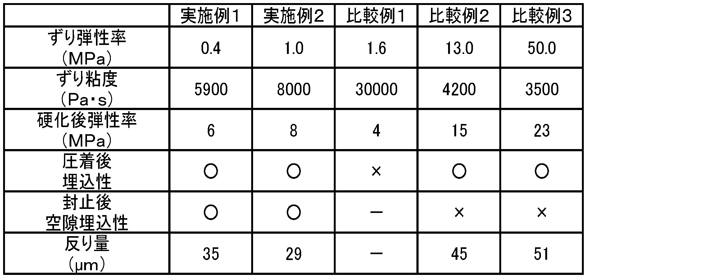
得られたフィルム状接着剤について下記のとおり評価をした。評価結果を表2に示す。
得られたフィルム状接着剤について下記のとおり評価をした。評価結果を表2に示す。
[ずり弾性率測定]
フィルム状接着剤から基材フィルムを剥離除去し、厚さ方向に10mm角に打ち抜いた。これを複数枚準備して貼り合わせることで、10mm角、厚さ360μmの、フィルム状接着剤の評価用サンプルを得た。動的粘弾性装置ARES(ティー・エイ・インスツルメント・ジャパン株式会社製)に直径8mmの円形アルミプレート治具をセットし、この冶具で上記評価用サンプルを挟み込んだ。その後、評価用サンプルに対し5%の歪みを周波数1Hzで与えながら、5℃/分の昇温速度で室温(30℃)から125℃まで昇温して1時間保持した後、5℃/分の昇温速度でさらに150℃まで昇温して45分間保持した。そして、150℃におけるずり弾性率の値を記録した。
フィルム状接着剤から基材フィルムを剥離除去し、厚さ方向に10mm角に打ち抜いた。これを複数枚準備して貼り合わせることで、10mm角、厚さ360μmの、フィルム状接着剤の評価用サンプルを得た。動的粘弾性装置ARES(ティー・エイ・インスツルメント・ジャパン株式会社製)に直径8mmの円形アルミプレート治具をセットし、この冶具で上記評価用サンプルを挟み込んだ。その後、評価用サンプルに対し5%の歪みを周波数1Hzで与えながら、5℃/分の昇温速度で室温(30℃)から125℃まで昇温して1時間保持した後、5℃/分の昇温速度でさらに150℃まで昇温して45分間保持した。そして、150℃におけるずり弾性率の値を記録した。
[ずり粘度測定]
ずり弾性率測定と同様にして、評価用サンプルに対し5%の歪みを周波数1Hzで与えながら、5℃/分の昇温速度で室温(30℃)から140℃まで昇温させながらずり粘度を測定した。そして、80℃での測定値を記録した。
ずり弾性率測定と同様にして、評価用サンプルに対し5%の歪みを周波数1Hzで与えながら、5℃/分の昇温速度で室温(30℃)から140℃まで昇温させながらずり粘度を測定した。そして、80℃での測定値を記録した。
[硬化後の引張弾性率測定]
フィルム状接着剤から基材フィルムを剥離除去した後、フィルム状接着剤を4mm幅、長さ30mmに切り出した。これを、120℃で2時間、170℃で3時間加熱し、フィルム状接着剤を硬化させた評価用サンプルを得た。その後、評価用サンプルを動的粘弾性装置(製品名:Rheogel-E4000、株式会社UMB製)にセットし、引張り荷重をかけて、周波数10Hz、昇温速度3℃/分の条件で引張弾性率を測定した。そして、170~190℃での測定値を記録した。
フィルム状接着剤から基材フィルムを剥離除去した後、フィルム状接着剤を4mm幅、長さ30mmに切り出した。これを、120℃で2時間、170℃で3時間加熱し、フィルム状接着剤を硬化させた評価用サンプルを得た。その後、評価用サンプルを動的粘弾性装置(製品名:Rheogel-E4000、株式会社UMB製)にセットし、引張り荷重をかけて、周波数10Hz、昇温速度3℃/分の条件で引張弾性率を測定した。そして、170~190℃での測定値を記録した。
[圧着後埋込性評価]
接着シートのフィルム状接着剤を2枚貼り合わせて厚さ120μmとし、これを厚さ100μmの半導体ウェハ(8インチ)に70℃で貼り付けた。次に、それらを7.5mm角にダイシングして、接着シート付き半導体素子を得た。
一方、ダイシング・ダイボンディング一体型フィルム(日立化成株式会社製、HR-9004-10(厚さ10μm))を、厚さ50μmの半導体ウェハ(8インチ)に70℃で貼り付けた。次に、それらを3.0mm角にダイシングして、上記の一体型フィルム付きチップを得た。一体型フィルム付きチップを、表面凹凸が最大6μmである評価用基板に、120℃、0.20MPa、2秒間の条件で圧着した後、120℃で2時間加熱して一体型フィルムを半硬化させた。これによりチップ付き基板を得た。
得られたチップ付き基板に、接着シート付き半導体素子を、120℃、0.20MPa、2秒間の条件で圧着した。この際、先に圧着しているチップが、接着シート付き半導体素子の真ん中にくるように位置合わせをした。得られた構造体を、ずり弾性率測定と同様にして125℃で1時間、150℃で45分間加熱した。
加熱後室温まで自然放冷した構造体を、超音波C-SCAN画像診断装置(インサイト株式会社製、品番IS350、プローブ:75MHz)にて分析し、圧着後埋込性を確認した。圧着後埋込性は以下の基準により評価した。
○:圧着フィルム面積に対する空隙面積の割合が10%未満。
×:圧着フィルム面積に対する空隙面積の割合が10%以上。
接着シートのフィルム状接着剤を2枚貼り合わせて厚さ120μmとし、これを厚さ100μmの半導体ウェハ(8インチ)に70℃で貼り付けた。次に、それらを7.5mm角にダイシングして、接着シート付き半導体素子を得た。
一方、ダイシング・ダイボンディング一体型フィルム(日立化成株式会社製、HR-9004-10(厚さ10μm))を、厚さ50μmの半導体ウェハ(8インチ)に70℃で貼り付けた。次に、それらを3.0mm角にダイシングして、上記の一体型フィルム付きチップを得た。一体型フィルム付きチップを、表面凹凸が最大6μmである評価用基板に、120℃、0.20MPa、2秒間の条件で圧着した後、120℃で2時間加熱して一体型フィルムを半硬化させた。これによりチップ付き基板を得た。
得られたチップ付き基板に、接着シート付き半導体素子を、120℃、0.20MPa、2秒間の条件で圧着した。この際、先に圧着しているチップが、接着シート付き半導体素子の真ん中にくるように位置合わせをした。得られた構造体を、ずり弾性率測定と同様にして125℃で1時間、150℃で45分間加熱した。
加熱後室温まで自然放冷した構造体を、超音波C-SCAN画像診断装置(インサイト株式会社製、品番IS350、プローブ:75MHz)にて分析し、圧着後埋込性を確認した。圧着後埋込性は以下の基準により評価した。
○:圧着フィルム面積に対する空隙面積の割合が10%未満。
×:圧着フィルム面積に対する空隙面積の割合が10%以上。
[封止後空隙埋込性評価]
圧着後埋込性評価にて得られた構造体の半導体素子等の搭載面を、モールド用封止材(日立化成株式会社製、商品名:CEL-9700HF)を用いて封止した。封止にはモールド成形機MH-705-1(アピックヤマダ株式会社製)を用い、封止条件は175℃、6.9MPa、120秒間とした。得られた封止サンプルを圧着後埋込性評価と同様に分析し、封止後空隙埋込性の評価を行った。評価基準は以下のとおりとした。
○:圧着フィルム面積に対する空隙面積の割合が5%未満。
×:圧着フィルム面積に対する空隙面積の割合が5%以上。
圧着後埋込性評価にて得られた構造体の半導体素子等の搭載面を、モールド用封止材(日立化成株式会社製、商品名:CEL-9700HF)を用いて封止した。封止にはモールド成形機MH-705-1(アピックヤマダ株式会社製)を用い、封止条件は175℃、6.9MPa、120秒間とした。得られた封止サンプルを圧着後埋込性評価と同様に分析し、封止後空隙埋込性の評価を行った。評価基準は以下のとおりとした。
○:圧着フィルム面積に対する空隙面積の割合が5%未満。
×:圧着フィルム面積に対する空隙面積の割合が5%以上。
[反り量の評価]
圧着後埋込性評価と同様にして構造体を作製した。この構造体を170℃で3時間加熱させて、フィルム状接着剤を硬化させた後、半導体素子の対角線方向における高低差を表面粗さ計で8mm分測定した。得られた測定値の最大値と最小値との差を、構造体の反り量として記録した。
圧着後埋込性評価と同様にして構造体を作製した。この構造体を170℃で3時間加熱させて、フィルム状接着剤を硬化させた後、半導体素子の対角線方向における高低差を表面粗さ計で8mm分測定した。得られた測定値の最大値と最小値との差を、構造体の反り量として記録した。
10…フィルム状接着剤、14…基板、42…樹脂(封止材)、88…第1のワイヤ、98…第2のワイヤ、200…半導体装置、Wa…第1の半導体素子、Waa…第2の半導体素子。
Claims (12)
- 基板上に第1のワイヤを介して第1の半導体素子を電気的に接続する第1のダイボンド工程と、
前記第1の半導体素子の面積よりも大きい第2の半導体素子の片面に、150℃におけるずり弾性率が1.5MPa以下であるフィルム状接着剤を貼付するラミネート工程と、
前記フィルム状接着剤が貼付された第2の半導体素子を、前記フィルム状接着剤が前記第1の半導体素子を覆うように載置し、前記フィルム状接着剤を圧着することで、前記第1のワイヤ及び前記第1の半導体素子を前記フィルム状接着剤に埋め込む第2のダイボンド工程と、
を備える、半導体装置の製造方法。 - 前記フィルム状接着剤の、硬化後の170~190℃における引張弾性率が15MPa以下である、請求項1に記載の製造方法。
- 前記フィルム状接着剤の、80℃におけるずり粘度が15000Pa・s以下である、請求項1又は2に記載の製造方法。
- 前記フィルム状接着剤が、アクリル樹脂及びエポキシ樹脂を含む、請求項1~3のいずれか一項に記載の製造方法。
- 前記アクリル樹脂が、重量平均分子量が10万~50万である第1のアクリル樹脂と、重量平均分子量が60万~100万である第2のアクリル樹脂とを含み、アクリル樹脂の全質量を基準として、前記第1のアクリル樹脂の含有量が50質量%以上である、請求項4に記載の製造方法。
- 前記フィルム状接着剤が、無機フィラー及び有機フィラーの少なくとも一方を含む、請求項1~5のいずれか一項に記載の製造方法。
- 基板上に第1のワイヤを介して第1の半導体素子が電気的に接続されると共に、前記第1の半導体素子上に、前記第1の半導体素子の面積よりも大きい第2の半導体素子が圧着されてなる半導体装置において、前記第2の半導体素子を圧着すると共に、前記第1のワイヤ及び前記第1の半導体素子を埋め込むために用いられる、150℃におけるずり弾性率が1.5MPa以下である、フィルム状接着剤。
- 硬化後における170~190℃における引張弾性率が15MPa以下である、請求項7に記載のフィルム状接着剤。
- 80℃におけるずり粘度が15000Pa・s以下である、請求項7又は8に記載のフィルム状接着剤。
- アクリル樹脂及びエポキシ樹脂を含む、請求項7~9のいずれか一項に記載のフィルム状接着剤。
- 前記アクリル樹脂が、重量平均分子量が10万~50万である第1のアクリル樹脂と、重量平均分子量が60万~100万である第2のアクリル樹脂とを含み、アクリル樹脂の全質量を基準として、前記第1のアクリル樹脂の含有量が50質量%以上である、請求項10に記載のフィルム状接着剤。
- 無機フィラー及び有機フィラーの少なくとも一方を含む、請求項7~11のいずれか一項に記載のフィルム状接着剤。
Priority Applications (6)
| Application Number | Priority Date | Filing Date | Title |
|---|---|---|---|
| JP2019568442A JP7140143B2 (ja) | 2018-01-30 | 2018-01-30 | 半導体装置の製造方法、及びフィルム状接着剤 |
| SG11202004664PA SG11202004664PA (en) | 2018-01-30 | 2018-01-30 | Semiconductor device production method and film-shaped adhesive |
| CN201880087166.8A CN111630641B (zh) | 2018-01-30 | 2018-01-30 | 半导体装置的制造方法及膜状粘接剂 |
| KR1020207019349A KR102450758B1 (ko) | 2018-01-30 | 2018-01-30 | 반도체 장치의 제조 방법, 및 필름형 접착제 |
| PCT/JP2018/003028 WO2019150449A1 (ja) | 2018-01-30 | 2018-01-30 | 半導体装置の製造方法、及びフィルム状接着剤 |
| TW108103014A TWI793255B (zh) | 2018-01-30 | 2019-01-28 | 半導體裝置的製造方法及膜狀接著劑 |
Applications Claiming Priority (1)
| Application Number | Priority Date | Filing Date | Title |
|---|---|---|---|
| PCT/JP2018/003028 WO2019150449A1 (ja) | 2018-01-30 | 2018-01-30 | 半導体装置の製造方法、及びフィルム状接着剤 |
Publications (1)
| Publication Number | Publication Date |
|---|---|
| WO2019150449A1 true WO2019150449A1 (ja) | 2019-08-08 |
Family
ID=67479182
Family Applications (1)
| Application Number | Title | Priority Date | Filing Date |
|---|---|---|---|
| PCT/JP2018/003028 Ceased WO2019150449A1 (ja) | 2018-01-30 | 2018-01-30 | 半導体装置の製造方法、及びフィルム状接着剤 |
Country Status (6)
| Country | Link |
|---|---|
| JP (1) | JP7140143B2 (ja) |
| KR (1) | KR102450758B1 (ja) |
| CN (1) | CN111630641B (ja) |
| SG (1) | SG11202004664PA (ja) |
| TW (1) | TWI793255B (ja) |
| WO (1) | WO2019150449A1 (ja) |
Cited By (1)
| Publication number | Priority date | Publication date | Assignee | Title |
|---|---|---|---|---|
| JP2023142901A (ja) * | 2022-03-25 | 2023-10-06 | 株式会社レゾナック | 半導体用接着フィルム、ダイシング・ダイボンディング一体型フィルム、及び半導体装置の製造方法 |
Citations (4)
| Publication number | Priority date | Publication date | Assignee | Title |
|---|---|---|---|---|
| JP2006005333A (ja) * | 2004-05-20 | 2006-01-05 | Toshiba Corp | 積層型電子部品とその製造方法 |
| JP2010118554A (ja) * | 2008-11-13 | 2010-05-27 | Nec Electronics Corp | 半導体装置およびその製造方法 |
| JP2013060524A (ja) * | 2011-09-13 | 2013-04-04 | Hitachi Chemical Co Ltd | フィルム状接着剤、接着シート、半導体装置及びその製造方法 |
| JP2015122425A (ja) * | 2013-12-24 | 2015-07-02 | 日東電工株式会社 | 半導体装置の製造方法、半導体装置、包埋用接着フィルム、及びダイシング・ダイボンドフィルム |
Family Cites Families (13)
| Publication number | Priority date | Publication date | Assignee | Title |
|---|---|---|---|---|
| JP3754475B2 (ja) * | 1995-10-31 | 2006-03-15 | スリーエム カンパニー | 反応性ホットメルト組成物、反応性ホットメルト組成物調製用組成物、フィルム状ホットメルト接着剤 |
| JP4788017B2 (ja) * | 1999-05-17 | 2011-10-05 | 株式会社デンソー | 膜の形成方法および電極あるいは配線の形成方法 |
| US6884833B2 (en) * | 2001-06-29 | 2005-04-26 | 3M Innovative Properties Company | Devices, compositions, and methods incorporating adhesives whose performance is enhanced by organophilic clay constituents |
| JP2005103180A (ja) | 2003-10-02 | 2005-04-21 | Matsushita Electric Ind Co Ltd | 洗濯機 |
| JP5524465B2 (ja) | 2007-10-24 | 2014-06-18 | 日立化成株式会社 | 接着シート及びこれを用いた半導体装置およびその製造方法 |
| JP2010254763A (ja) * | 2009-04-22 | 2010-11-11 | Hitachi Chem Co Ltd | 接着剤組成物、その製造方法、これを用いた接着シート、一体型シート、その製造方法、半導体装置及びその製造方法 |
| JP5879675B2 (ja) * | 2010-06-17 | 2016-03-08 | 日立化成株式会社 | 半導体用接着フィルム、半導体搭載用配線基板、半導体装置、および接着剤組成物 |
| JP6133542B2 (ja) | 2012-02-29 | 2017-05-24 | 日立化成株式会社 | フィルム状接着剤、接着シート及び半導体装置 |
| CN104169383B (zh) * | 2012-03-08 | 2016-11-09 | 日立化成株式会社 | 粘接片材及半导体装置的制造方法 |
| JP5924145B2 (ja) | 2012-06-12 | 2016-05-25 | 日立化成株式会社 | フィルム状接着剤、接着シート、及び半導体装置の製造方法 |
| JP5890795B2 (ja) * | 2013-03-18 | 2016-03-22 | 日本碍子株式会社 | 半導体製造装置用部材 |
| KR101974466B1 (ko) * | 2015-03-23 | 2019-05-02 | 후지필름 가부시키가이샤 | 적층체, 가접착용 조성물 및 가접착막 |
| JP6819597B2 (ja) * | 2015-09-07 | 2021-01-27 | 昭和電工マテリアルズ株式会社 | 接合体及び半導体装置 |
-
2018
- 2018-01-30 WO PCT/JP2018/003028 patent/WO2019150449A1/ja not_active Ceased
- 2018-01-30 JP JP2019568442A patent/JP7140143B2/ja active Active
- 2018-01-30 KR KR1020207019349A patent/KR102450758B1/ko active Active
- 2018-01-30 CN CN201880087166.8A patent/CN111630641B/zh active Active
- 2018-01-30 SG SG11202004664PA patent/SG11202004664PA/en unknown
-
2019
- 2019-01-28 TW TW108103014A patent/TWI793255B/zh active
Patent Citations (4)
| Publication number | Priority date | Publication date | Assignee | Title |
|---|---|---|---|---|
| JP2006005333A (ja) * | 2004-05-20 | 2006-01-05 | Toshiba Corp | 積層型電子部品とその製造方法 |
| JP2010118554A (ja) * | 2008-11-13 | 2010-05-27 | Nec Electronics Corp | 半導体装置およびその製造方法 |
| JP2013060524A (ja) * | 2011-09-13 | 2013-04-04 | Hitachi Chemical Co Ltd | フィルム状接着剤、接着シート、半導体装置及びその製造方法 |
| JP2015122425A (ja) * | 2013-12-24 | 2015-07-02 | 日東電工株式会社 | 半導体装置の製造方法、半導体装置、包埋用接着フィルム、及びダイシング・ダイボンドフィルム |
Cited By (2)
| Publication number | Priority date | Publication date | Assignee | Title |
|---|---|---|---|---|
| JP2023142901A (ja) * | 2022-03-25 | 2023-10-06 | 株式会社レゾナック | 半導体用接着フィルム、ダイシング・ダイボンディング一体型フィルム、及び半導体装置の製造方法 |
| JP7848546B2 (ja) | 2022-03-25 | 2026-04-21 | 株式会社レゾナック | 半導体用接着フィルム、ダイシング・ダイボンディング一体型フィルム、及び半導体装置の製造方法 |
Also Published As
| Publication number | Publication date |
|---|---|
| TW201939622A (zh) | 2019-10-01 |
| JP7140143B2 (ja) | 2022-09-21 |
| CN111630641A (zh) | 2020-09-04 |
| KR102450758B1 (ko) | 2022-10-04 |
| SG11202004664PA (en) | 2020-06-29 |
| CN111630641B (zh) | 2023-05-02 |
| JPWO2019150449A1 (ja) | 2021-01-28 |
| TWI793255B (zh) | 2023-02-21 |
| KR20200112828A (ko) | 2020-10-05 |
Similar Documents
| Publication | Publication Date | Title |
|---|---|---|
| JP6135202B2 (ja) | 半導体装置及び半導体装置の製造方法 | |
| JP5736899B2 (ja) | フィルム状接着剤、接着シート及び半導体装置 | |
| JP6133542B2 (ja) | フィルム状接着剤、接着シート及び半導体装置 | |
| JP5428423B2 (ja) | 半導体装置及びフィルム状接着剤 | |
| JP5834662B2 (ja) | フィルム状接着剤、接着シート、半導体装置及びその製造方法 | |
| JP6222395B1 (ja) | フィルム状接着剤及びダイシングダイボンディング一体型接着シート | |
| JP6191799B1 (ja) | 半導体装置、半導体装置の製造方法及びフィルム状接着剤 | |
| JP6443521B2 (ja) | フィルム状接着剤及びダイシングダイボンディング一体型接着シート | |
| JP2012153851A (ja) | 半導体装置及びフィルム状接着剤 | |
| TWI785197B (zh) | 半導體裝置的製造方法及膜狀接著劑 | |
| TWI774916B (zh) | 半導體裝置的製造方法、膜狀接著劑及接著片 | |
| JP6191800B1 (ja) | フィルム状接着剤及びダイシングダイボンディング一体型接着シート | |
| TWI852922B (zh) | 半導體裝置的製造方法 | |
| JP7140143B2 (ja) | 半導体装置の製造方法、及びフィルム状接着剤 | |
| JP6213618B2 (ja) | フィルム状接着剤、接着シート及び半導体装置 |
Legal Events
| Date | Code | Title | Description |
|---|---|---|---|
| 121 | Ep: the epo has been informed by wipo that ep was designated in this application |
Ref document number: 18904003 Country of ref document: EP Kind code of ref document: A1 |
|
| ENP | Entry into the national phase |
Ref document number: 2019568442 Country of ref document: JP Kind code of ref document: A |
|
| NENP | Non-entry into the national phase |
Ref country code: DE |
|
| 122 | Ep: pct application non-entry in european phase |
Ref document number: 18904003 Country of ref document: EP Kind code of ref document: A1 |