WO2019148952A1 - 获得刻蚀深度极限值的方法 - Google Patents
获得刻蚀深度极限值的方法 Download PDFInfo
- Publication number
- WO2019148952A1 WO2019148952A1 PCT/CN2018/117824 CN2018117824W WO2019148952A1 WO 2019148952 A1 WO2019148952 A1 WO 2019148952A1 CN 2018117824 W CN2018117824 W CN 2018117824W WO 2019148952 A1 WO2019148952 A1 WO 2019148952A1
- Authority
- WO
- WIPO (PCT)
- Prior art keywords
- limit value
- data
- etch
- average
- process cycles
- Prior art date
- Legal status (The legal status is an assumption and is not a legal conclusion. Google has not performed a legal analysis and makes no representation as to the accuracy of the status listed.)
- Ceased
Links
Images
Classifications
-
- G—PHYSICS
- G06—COMPUTING OR CALCULATING; COUNTING
- G06F—ELECTRIC DIGITAL DATA PROCESSING
- G06F17/00—Digital computing or data processing equipment or methods, specially adapted for specific functions
- G06F17/10—Complex mathematical operations
- G06F17/11—Complex mathematical operations for solving equations, e.g. nonlinear equations, general mathematical optimization problems
-
- H—ELECTRICITY
- H10—SEMICONDUCTOR DEVICES; ELECTRIC SOLID-STATE DEVICES NOT OTHERWISE PROVIDED FOR
- H10P—GENERIC PROCESSES OR APPARATUS FOR THE MANUFACTURE OR TREATMENT OF DEVICES COVERED BY CLASS H10
- H10P74/00—Testing or measuring during manufacture or treatment of wafers, substrates or devices
- H10P74/20—Testing or measuring during manufacture or treatment of wafers, substrates or devices characterised by the properties tested or measured, e.g. structural or electrical properties
- H10P74/203—Structural properties, e.g. testing or measuring thicknesses, line widths, warpage, bond strengths or physical defects
-
- H—ELECTRICITY
- H10—SEMICONDUCTOR DEVICES; ELECTRIC SOLID-STATE DEVICES NOT OTHERWISE PROVIDED FOR
- H10P—GENERIC PROCESSES OR APPARATUS FOR THE MANUFACTURE OR TREATMENT OF DEVICES COVERED BY CLASS H10
- H10P74/00—Testing or measuring during manufacture or treatment of wafers, substrates or devices
- H10P74/23—Testing or measuring during manufacture or treatment of wafers, substrates or devices characterised by multiple measurements, corrections, marking or sorting processes
Definitions
- the present invention relates to the field of microelectronics, and in particular to a method for obtaining an etch depth limit.
- Deep silicon etching technology has a wide range of important applications in the microelectronics industry. For example, in the field of integrated circuit manufacturing, deep silicon etching is required to make deep via holes in the interlayer film between two interconnected metal lines. Interconnecting metal is filled in the deep via to connect the transistors into a functional device loop. As another example, in the field of packaging, Through Silicon Vias (TSV) technology is still the mainstream packaging method for improving device performance, reducing power consumption, and reducing device size.
- TSV Through Silicon Vias
- the Bosch process is currently the mainstream process for deep silicon etching.
- the basic principle is to first form a polymer protective layer on the sidewall of the pattern to be etched, and then simultaneously etch the polymer protective layer and the material to be etched by chemical reaction. Through the cycle of etching and deposition, anisotropic deep silicon etching is finally realized.
- the plasma plays a very critical role, and due to factors such as plasma concentration and mean free path, any deep silicon etch has a limit etch depth under certain conditions.
- the present invention aims to at least solve one of the technical problems existing in the prior art, and proposes a method for obtaining an etch depth limit value, which can obtain a limit value of an etch depth using a small number of trials, thereby simplifying the method. ,cut costs.
- a method for obtaining an etch depth limit value comprising the steps of:
- S1 input at least three sets of data, each set of data including an etch depth value and a number of process cycles;
- a linear equation representing the relationship between the average etch rate and the process cycle is fitted by a linear fitting method
- step S4 a quadratic curve indicating the relationship between the etching depth and the number of process cycles is obtained according to the linear equation, and the limit value of the etching depth is obtained according to the quadratic curve calculation.
- a is a quadratic coefficient
- b is a quadratic coefficient
- a variable y represents the average etch rate
- a variable x represents the number of process cycles
- m 1, 2, ..., m
- m m is the number of groups of the data
- x i the number of process cycles in the i-th data
- y i the average etch in the i-th data rate
- the average of the number of process cycles in the m group of data The average of the average etch rates in the m sets of data.
- variable h represents the etching depth and the variable n represents the number of process cycles.
- the method further includes a step S3', which is performed before or after the step S3, or simultaneously with the step S3; the step S3' includes:
- step S32' determining whether the linear correlation coefficient is greater than or equal to a preset achievement value; if yes, proceeding to step S3, and if not, proceeding to step S33';
- step S33' determine whether the data is greater than three groups, and if so, proceed to step S34', and if not, return to perform the step S1;
- Step S34' select any three sets of data to perform the step S31', and determine whether the linear correlation coefficient is greater than or equal to the preset achievement value; if yes, proceed to the step S3; if not, return to perform the Step S1.
- a linear correlation coefficient between the average etch rate and the number of process cycles is calculated according to the following formula:
- the preset compliance value is 0.97.
- the at least three sets of data are obtained by performing the test of the corresponding number of groups, and the number of the process cycles used in the test corresponding to the different sets of data is different, and the other process parameters are the same.
- the test comprises a deposition step and an etching step, the number of process cycles being the number of times the deposition step and the etching step are performed cyclically.
- the method is applied to a deep silicon etch process.
- the method for obtaining an etch depth limit value according to the present invention calculates an average etch rate in each group of data according to at least three sets of data including an etch depth value and a number of process cycles, and fits by using a fitting method.
- the relationship between the average etching rate and the number of process cycles is obtained, and then the relationship between the etching depth and the number of process cycles is obtained according to the relationship, and the limit value of the etching depth is calculated based on the relationship between the etching depth and the number of process cycles. Since the limit value of the etching depth can be obtained by performing only at least three tests, the method for obtaining the etching depth limit value provided by the present invention is simple and low in cost.
- the method can automatically obtain the etch depth limit value by inputting the data with a small number of groups, thereby realizing automation.
- the method for obtaining the etch depth limit value provided by the present invention is not limited by the type of the device and the feature size, and has a wide application range.
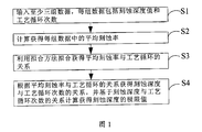
- FIG. 1 is a flow chart of a method for obtaining an etch depth limit value according to an embodiment of the present invention
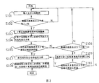
- FIG. 2 is another flow chart of a method for obtaining an etch depth limit value according to an embodiment of the present invention
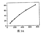
- 3A is a graph of etching depth values and number of process cycles
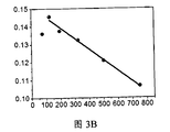
- 3B is a graph of average etch rate and number of process cycles
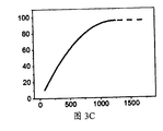
- Figure 3C is a graph of the maximum value of the etch depth.
- a method for obtaining an etch depth limit value includes the following steps:
- S1 input at least three sets of data, each set of data including an etch depth value and a corresponding number of process cycles;
- the relationship between the etching depth and the number of process cycles is obtained according to the relationship between the average etching rate and the process cycle, and the limit value of the etching depth is calculated based on the relationship between the etching depth and the number of process cycles.
- the method for obtaining the etch depth limit value provided by the embodiment of the present invention is simple and low in cost, since the etching depth limit value can be obtained only by performing at least three tests. Moreover, the method can automatically obtain the etch depth limit value by inputting the data with a small number of groups, thereby realizing automation. In addition, the method for obtaining the etch depth limit value provided by the embodiment of the present invention is not limited by the type of the device and the feature size, and the application range is wide.
- step S3 a linear equation representing the relationship between the average etching rate and the process cycle is fitted by a linear fitting method.
- variable y represents the average etch rate
- variable x represents the number of process cycles
- a is a quadratic coefficient
- b is a quadratic coefficient
- i 1, 2, ..., m
- m is the number of groups of data
- x i is the number of process cycles in the i-th data
- y i is The specified parameter value in the i-th data; The average of the number of process cycles in at least three sets of data; The average of the specified parameter values in at least three sets of data.
- step S4 a quadratic curve indicating the relationship between the etching depth and the number of process cycles is obtained according to the linear equation, and the limit value of the etching depth is obtained from the calculation of the quadratic curve.
- variable h represents the etching depth
- variable n represents the number of process cycles
- the extremum derivation process is:
- the method includes the following steps:
- S101 Input at least three sets of data, where each set of data includes an etch depth value and a corresponding number of process cycles.
- step S102 Determine whether the number of groups of data is greater than or equal to three groups. If yes, proceed to step S103; if no, return to step S101.
- step S105 Determine whether the linear correlation coefficient is greater than or equal to a preset target value; if yes, proceed to step S107; if no, proceed to step S106.
- step S106 It is determined whether the number of groups of data is greater than three groups, and if yes, proceed to step S109; if no, return to step S101.
- step S110 determining whether the linear correlation coefficient is greater than or equal to a preset target value; if yes, proceeding to step S107; if not, returning to step S101.
- step S2 the calculation and determination process of the linearity of the average etch rate in the three sets of data is added, which may be performed simultaneously with the above step S3, or may also be in the step Before or after S3.
- a linear correlation coefficient between the average etching rate and the number of process cycles is calculated according to the following formula
- step S105 it is determined whether the linear correlation coefficient is greater than or equal to a preset target value, and if yes, proceed to step S107; if not, proceed to step S106.
- the above preset target value may be 0.97.
- a method for obtaining an etch depth limit value provided by an embodiment of the present invention can be applied to a deep silicon etch process. Specifically, at least three sets of data can be obtained by performing tests on the corresponding number of groups, and the number of process cycles used in each set of tests is different, and other parameters are the same. Moreover, each set of tests includes a deposition step and an etching step, and the number of process cycles is the number of times the deposition step and the etching step are performed cyclically.
- Table 1 the process recipe of the 6 sets of etching process tests.
- the abscissa is the number of process cycles; the ordinate is the etch depth; 6 points are obtained according to the number of process cycles and the etch depth in the 6 sets of data, and the etch depth and the number of process cycles are obtained by point-by-point connection. curve.
- the abscissa is the number of process cycles; the ordinate is the average etch rate; 6 points are obtained according to the number of process cycles and the average etch rate in the 6 sets of data, and the average etch rate and process are obtained by point-by-point connection. The curve of the number of cycles. Since the first point deviates significantly from the linear region, the first point is rejected.
- a linear equation is used to fit a linear equation of the relationship between the average etch rate and the number of process cycles; then, a quadratic curve of the relationship between the etch depth and the number of process cycles is obtained according to the linear equation, and according to the second
- the secondary curve calculates the maximum value of the etch depth.
- the maximum etching depth of the deep silicon trench obtained by the above method is about 94.2 ⁇ m; as shown in FIG. 3C, the ordinate is the etching depth; the abscissa is The number of process cycles.
- the curve is a curve of the etching depth of the deep silicon trench obtained by testing infinitely increasing the number of process cycles (1500 or more), and the etching depth can be up to 94.2 ⁇ m, which is the maximum value obtained by the method of the present invention. Match.
- the method for obtaining the etch depth limit value provided by the present invention only needs to perform at least three tests to obtain the limit value of the etch depth, which is simple and low in cost. Moreover, the method can automatically obtain the etch depth limit value by inputting the data with a small number of groups, thereby realizing automation. In addition, the method for obtaining the etch depth limit value provided by the present invention is not limited by the type of the device and the feature size, and has a wide application range.
Landscapes
- Engineering & Computer Science (AREA)
- Physics & Mathematics (AREA)
- Mathematical Physics (AREA)
- General Physics & Mathematics (AREA)
- Pure & Applied Mathematics (AREA)
- Mathematical Optimization (AREA)
- Mathematical Analysis (AREA)
- Computational Mathematics (AREA)
- Data Mining & Analysis (AREA)
- Theoretical Computer Science (AREA)
- Operations Research (AREA)
- Algebra (AREA)
- Databases & Information Systems (AREA)
- Software Systems (AREA)
- General Engineering & Computer Science (AREA)
- Drying Of Semiconductors (AREA)
- Testing Or Measuring Of Semiconductors Or The Like (AREA)
Abstract
本发明提供一种获得刻蚀深度极限值的方法,包括以下步骤:S1,输入至少三组数据,每组数据包括刻蚀深度值和对应的工艺循环次数;S2,计算各组数据中的平均刻蚀率,该平均刻蚀率为刻蚀深度值与工艺循环次数的比值;S3,利用拟合方法拟合获得平均刻蚀率与工艺循环的关系;S4,根据平均刻蚀率与工艺循环的关系获得刻蚀深度与工艺循环次数的关系,并基于刻蚀深度与工艺循环次数的关系计算获得刻蚀深度的极限值。本发明提供的获得刻蚀深度极限值的方法,其可以采用较少的试验次数获得刻蚀深度极限值,从而可以简化方法,降低成本。
Description
本发明涉及微电子技术领域,具体地,涉及一种获得刻蚀深度极限值的方法。
深硅刻蚀技术在微电子产业中具有广泛而重要的应用,例如,在集成电路制造领域,需要采用深硅刻蚀技术在两层互联金属线之间的层间膜内制作深通孔,并在该深通孔中填入互联金属,以将晶体管连接成具有一定功能的器件回路。又如,在封装领域,硅通孔(Through Silicon Vias,TSV)技术仍然是提升器件性能、降低功耗和减小器件体积的主流封装方法。
对于具有较大深宽比的孔,很难采用传统的湿法刻蚀制作,必须采用干法刻蚀。Bosch工艺是目前实现深硅刻蚀的主流工艺方法,其基本原理是:首先在待刻蚀的图形侧壁形成聚合物保护层,然后利用化学反应同时刻蚀聚合物保护层和待刻蚀材料,经过刻蚀与沉积的循环进行,最终实现各向异性的深硅刻蚀。在该过程中,等离子体起到非常关键的作用,而受限于等离子体的浓度和平均自由程等因素的影响,任何深硅刻蚀在特定条件下都存在一个极限刻蚀深度。
探知刻蚀机的极限刻蚀深度对于器件设计、生产过程异常排查和机台维护等诸多方面都有重要的意义。目前,获得极限刻蚀深度需要逐片进行工艺,这极大地增加了成本,而且还有可能无法获得测试结果。
因此,如何通过简便的低成本方法估算出刻蚀机的极限刻蚀深度是目前亟待解决的问题。
发明内容
本发明旨在至少解决现有技术中存在的技术问题之一,提出了一种获得刻蚀深度极限值的方法,其可以采用较少的试验次数获得刻蚀深度的极限值,从而可以简化方法,降低成本。
为实现本发明的目的而提供一种获得刻蚀深度极限值的方法,包括以下步骤:
S1,输入至少三组数据,每组数据包括刻蚀深度值和工艺循环次数;
S2,计算获得每组所述数据中的平均刻蚀率,所述平均刻蚀率为所述刻蚀深度值与所述工艺循环次数的比值;
S3,利用拟合方法拟合获得所述平均刻蚀率与所述工艺循环的关系;
S4,根据所述平均刻蚀率与所述工艺循环的关系获得刻蚀深度与工艺循环次数的关系,并基于所述刻蚀深度与工艺循环次数的关系计算获得刻蚀深度的极限值。
可选的,在所述步骤S3中,利用线性拟合方法拟合出表示所述平均刻蚀率与所述工艺循环的关系的线性方程;
在所述步骤S4中,根据所述线性方程获得表示刻蚀深度与工艺循环次数的关系的二次曲线,并根据所述二次曲线计算获得刻蚀深度的极限值。
可选的,在所述步骤S3中,所述线性拟合方法包括最小二乘法;所述线性方程为:y=ax+b;
其中,a为二次方系数;b为一次方系数;变量y代表所述平均刻蚀率;变量x代表所述工艺循环次数;并且,


其中,i=1,2,...,m,m为所述数据的组数;x
i为第i组数据中的工艺循环次 数;y
i为第i组数据中的所述平均刻蚀率;
 为m组数据中所述工艺循环次数的平均值;
 为m组数据中所述平均刻蚀率的平均值。
可选的,在所述步骤S4中,所述二次曲线为:h=an
2+bn;
其中,变量h代表所述刻蚀深度,变量n代表所述工艺循环次数。
可选的,在所述步骤S4中,对所述二次曲线求极值,获得所述刻蚀深度的极限值为:h
limit=-b
2/4a。
可选的,所述方法还包括步骤S3’,所述步骤S3’在所述步骤S3之前或者之后进行,或者与所述步骤S3同时进行;所述步骤S3’包括:
S31’,计算各组数据中所述平均刻蚀率与所述工艺循环次数的线性相关系数;
S32’,判断该线性相关系数是否大于或者等于预设达标值;若是,则进行所述步骤S3,若否,则进行步骤S33’;
S33’,判断所述数据是否大于三组,若是,则进行步骤S34’,若否,则返回执行所述步骤S1;
S34’,选择任意三组数据来执行所述步骤S31’,且判断该线性相关系数是否大于或者等于所述预设达标值;若是,则进行所述步骤S3;若否,则返回执行所述步骤S1。
可选的,在所述步骤S31’中,根据下述公式计算所述平均刻蚀率与所述工艺循环次数的线性相关系数:

其中,X为工艺循环次数;Y为平均刻蚀率;r(X,Y)为线性相关系数;Cov(X,Y)为X和Y的协方差;Var(X)为X的方差;Var(Y)为Y的方差。
可选的,所述预设达标值为0.97。
可选的,所述至少三组数据通过进行对应组数的试验获得,不同组数据 对应的试验采用的所述工艺循环次数不同,而其他工艺参数均相同。
可选的,所述试验包括沉积步骤和刻蚀步骤,所述工艺循环次数为循环进行所述沉积步骤和刻蚀步骤的次数。
可选的,该方法应用于深硅刻蚀工艺中。
本发明具有以下有益效果:
本发明提供的获得刻蚀深度极限值的方法,其根据输入的包含刻蚀深度值和工艺循环次数的至少三组数据,计算各组数据中的平均刻蚀率,并利用拟合方法拟合获得平均刻蚀率与工艺循环次数的关系,然后根据该关系获得刻蚀深度与工艺循环次数的关系,并基于刻蚀深度与工艺循环次数的关系计算获得刻蚀深度的极限值。由于只需要进行至少三次试验即可获得刻蚀深度的极限值,本发明提供的获得刻蚀深度极限值的方法较简便,且成本较低。而且,该方法通过输入组数较少的数据,即可自动获得刻蚀深度极限值,从而实现了自动化。另外,本发明提供的获得刻蚀深度极限值的方法不受器件种类和特征尺寸的局限,应用范围较广。
图1为本发明实施例提供的获得刻蚀深度极限值的方法的一种流程框图;
图2为本发明实施例提供的获得刻蚀深度极限值的方法的另一种流程框图;
图3A为刻蚀深度值与工艺循环次数的曲线图;
图3B为平均刻蚀率与工艺循环次数的曲线图;
图3C为刻蚀深度的极大值的曲线图。
为使本领域的技术人员更好地理解本发明的技术方案,下面结合附图来 对本发明提供的获得刻蚀深度极限值的方法进行详细描述。
请参阅图1,本发明实施例提供的获得刻蚀深度极限值的方法,其包括以下步骤:
S1,输入至少三组数据,每组数据包括刻蚀深度值和对应的工艺循环次数;
S2,计算各组数据中的平均刻蚀率,该平均刻蚀率为刻蚀深度值与工艺循环次数的比值;
S3,利用拟合方法拟合获得平均刻蚀率与工艺循环的关系;
S4,根据平均刻蚀率与工艺循环的关系获得刻蚀深度与工艺循环次数的关系,并基于刻蚀深度与工艺循环次数的关系计算获得刻蚀深度的极限值。
由于只需要进行至少三次试验即可获得刻蚀深度极限值,本发明实施例提供的获得刻蚀深度极限值的方法较简便,且成本较低。而且,该方法通过输入组数较少的数据,即可自动获得刻蚀深度极限值,从而实现了自动化。另外,本发明实施例提供的获得刻蚀深度极限值的方法不受器件种类和特征尺寸的局限,应用范围较广。
在上述步骤S3中,利用线性拟合方法拟合出表示平均刻蚀率与工艺循环的关系的线性方程。
在进行线性拟合时,可以剔除明显偏离线性区域的点,然后建立线性方程。
可选的,线性拟合的方法包括最小二乘法;获得的线性方程为:y=ax+b;
其中,变量y代表平均刻蚀率;变量x代表工艺循环次数,并且,


其中,a为二次方系数;b为一次方系数;i=1,2,...,m,m为数据的组数;x
i 为第i组数据中的工艺循环次数;y
i为第i组数据中的指定参数值;
 为至少三组数据中的工艺循环次数的平均值;
 为至少三组数据中的指定参数值的平均值。
在上述步骤S4中,根据线性方程获得表示刻蚀深度与工艺循环次数的关系的二次曲线,并根据该二次曲线计算获得刻蚀深度的极限值。
具体地,获得的刻蚀深度与工艺循环次数之间关系的二次曲线为:h=an
2+bn;
其中,变量h代表刻蚀深度,变量n代表工艺循环次数。
可选的,在上述步骤S4中,对二次曲线(h=an
2+bn)求极值,获得刻蚀深度的极限值为:h
limit=-b
2/4a。
具体地,极值推导过程为:
h=an
2+bn
h=a(n
2+bn/a)
h=a(n
2+bn/a+b
2/4a
2-b
2/4a
2)
h=a(n
2+bn/a+b
2/4a
2)-b
2/4a
h=a(n+b/2a)
2-b
2/4a
由于(n+b/2a)
2是一个非负数,其最小值为0,因此在(n+b/2a)
2=0时,可以得到h
limit=-b
2/4a。
下面对本发明提供的获得刻蚀深度极限值的方法的具体实施方式进行详细描述。具体地,请参阅图2,该方法包括以下步骤:
S101,输入至少三组数据,每组数据包括刻蚀深度值和对应的工艺循环次数。
S102,判断数据的组数是否大于或者等于三组,若是,则进行步骤S103;若否,则返回步骤S101。
S103,计算各组数据中的平均刻蚀率,该平均刻蚀率为刻蚀深度值与工艺循环次数的比值;
S104,计算各组数据中的平均刻蚀率与工艺循环次数之间的线性相关系数;
S105,判断该线性相关系数是否大于或者等于预设达标值;若是,则进行步骤S107;若否,则进行步骤S106。
S106,判断数据的组数是否大于三组,若是,则进行步骤S109;若否,则返回执行步骤S101。
S107,利用线性拟合的方法拟合出平均刻蚀率与工艺循环次数之间关系的线性方程。
S108,根据线性方程获得刻蚀深度与工艺循环次数之间关系的二次曲线,并根据二次曲线计算刻蚀深度的极限值。
S109,选择任意三组数据来执行步骤104;
S110,判断该线性相关系数是否大于或者等于预设达标值;若是,则进行步骤S107;若否,则返回执行步骤S101。
由上可知,在步骤S2之后,且在步骤S3之前,增加了三组数据中的平均刻蚀率的线性度的计算和判断过程,该过程可以与上述步骤S3同时进行,或者也可以在步骤S3之前或者之后进行。
具体地,在上述步骤S104中,根据下述公式计算平均刻蚀率与工艺循环次数之间的线性相关系数;

其中,X为工艺循环次数;Y为平均刻蚀率;r(X,Y)为线性相关系数;Cov(X,Y)为X和Y的协方差;Var(X)为X的方差;Var(Y)为Y的方差。
在上述步骤S105中,判断上述线性相关系数是否大于或者等于预设达标值,若是,则进行步骤S107;若否,则进行步骤S106。
在实际应用中,上述预设达标值可以为0.97。
本发明实施例提供的获得刻蚀深度极限值的方法,其可以应用于深硅刻蚀工艺中。具体地,至少三组数据可以通过进行对应组数的试验获得,各组试验采用的工艺循环次数不同,而其他参数均相同。而且,每组试验包括沉积步骤和刻蚀步骤,工艺循环次数为循环进行沉积步骤和刻蚀步骤的次数。
以数据的组数为6组为例,6组刻蚀工艺试验的工艺配方如表1所示;6组数据及指定参数值的平均值如表2所示。
表1,6组刻蚀工艺试验的工艺配方。

表2,6组刻蚀工艺的数据结果。

请参阅图3A,横坐标为工艺循环次数;纵坐标为刻蚀深度;根据6组数据中的工艺循环次数和刻蚀深度获得6个点,逐点连线获得刻蚀深度与工艺循环次数的曲线。
请参阅图3B,横坐标为工艺循环次数;纵坐标为平均刻蚀率;根据6 组数据中的工艺循环次数和平均刻蚀率获得6个点,逐点连线获得平均刻蚀率与工艺循环次数的曲线。由于第一个点明显偏离线性区域,将第一个点剔除。
利用线性拟合的方法拟合出平均刻蚀率与工艺循环次数之间关系的线性方程;然后,根据该线性方程获得刻蚀深度与工艺循环次数之间关系的二次曲线,并根据该二次曲线计算刻蚀深度的极大值。以特征尺寸为5μm的深硅槽刻蚀为例,采用上述方法获得的深硅槽的刻蚀深度极大值大约为94.2μm;如图3C所示,纵坐标为刻蚀深度;横坐标为工艺循环次数。该曲线为采用无限增大工艺循环次数(1500以上)进行试验获得的深硅槽的刻蚀深度的曲线,该刻蚀深度最大能够达到94.2μm,与采用本发明的方法获得的极大值相吻合。
综上所述,本发明提供的获得刻蚀深度极限值的方法,其只需要进行至少三次试验即可获得刻蚀深度的极限值,较简便,且成本较低。而且,该方法通过输入组数较少的数据,即可自动获得刻蚀深度极限值,从而实现了自动化。另外,本发明提供的获得刻蚀深度极限值的方法不受器件种类和特征尺寸的局限,应用范围较广。
以上实施方式仅仅是为了说明本发明的原理而采用的示例性实施方式,然而本发明并不局限于此。对于本领域内的普通技术人员而言,在不脱离本发明的精神和实质的情况下,可以做出各种变型和改进,这些变型和改进也视为本发明的保护范围。
Claims (11)
- 一种获得刻蚀深度极限值的方法,其特征在于,包括以下步骤:S1,输入至少三组数据,每组数据包括刻蚀深度值和工艺循环次数;S2,计算获得每组所述数据中的平均刻蚀率,所述平均刻蚀率为所述刻蚀深度值与所述工艺循环次数的比值;S3,利用拟合方法拟合获得所述平均刻蚀率与所述工艺循环的关系;S4,根据所述平均刻蚀率与所述工艺循环的关系获得刻蚀深度与工艺循环次数的关系,并基于所述刻蚀深度与工艺循环次数的关系计算获得刻蚀深度的极限值。
- 根据权利要求1所述的获得刻蚀深度极限值的方法,其特征在于,在所述步骤S3中,利用线性拟合方法拟合出表示所述平均刻蚀率与所述工艺循环的关系的线性方程;在所述步骤S4中,根据所述线性方程获得表示刻蚀深度与工艺循环次数的关系的二次曲线,并根据所述二次曲线计算获得刻蚀深度的极限值。
- 根据权利要求2所述的获得刻蚀深度极限值的方法,其特征在于,在所述步骤S3中,所述线性拟合方法包括最小二乘法;所述线性方程为:y=ax+b;其中,a为二次方系数;b为一次方系数;变量y代表所述平均刻蚀率;变量x代表所述工艺循环次数;并且,

 其中,i=1,2,...,m,m为所述数据的组数;x i为第i组数据中的工艺循环次 数;y i为第i组数据中的所述平均刻蚀率;为m组数据中所述工艺循环次数的平均值;
 为m组数据中所述平均刻蚀率的平均值。
- 根据权利要求3所述的获得刻蚀深度极限值的方法,其特征在于,在所述步骤S4中,所述二次曲线为:h=an 2+bn;其中,变量h代表所述刻蚀深度,变量n代表所述工艺循环次数。
- 根据权利要求4所述的获得刻蚀深度极限值的方法,其特征在于,在所述步骤S4中,对所述二次曲线求极值,获得所述刻蚀深度的极限值为:h limit=-b 2/4a。
- 根据权利要求1所述的获得刻蚀深度极限值的方法,其特征在于,所述方法还包括步骤S3’,所述步骤S3’在所述步骤S3之前或者之后进行,或者与所述步骤S3同时进行;所述步骤S3’包括:S31’,计算各组数据中所述平均刻蚀率与所述工艺循环次数的线性相关系数;S32’,判断该线性相关系数是否大于或者等于预设达标值;若是,则进行所述步骤S3,若否,则进行步骤S33’;S33’,判断所述数据是否大于三组,若是,则进行步骤S34’,若否,则返回执行所述步骤S1;S34’,选择任意三组数据来执行所述步骤S31’,且判断该线性相关系数是否大于或者等于所述预设达标值;若是,则进行所述步骤S3;若否,则返回执行所述步骤S1。
- 根据权利要求6所述的获得刻蚀深度极限值的方法,其特征在于,在所述步骤S31’中,根据下述公式计算所述平均刻蚀率与所述工艺循环次数 的线性相关系数:
 其中,X为工艺循环次数;Y为平均刻蚀率;r(X,Y)为线性相关系数;Cov(X,Y)为X和Y的协方差;Var(X)为X的方差;Var(Y)为Y的方差。
 - 根据权利要求6或7所述的获得刻蚀深度极限值的方法,其特征在于,所述预设达标值为0.97。
- 根据权利要求1所述的获得刻蚀深度极限值的方法,其特征在于,所述至少三组数据通过进行对应组数的试验获得,不同组数据对应的试验采用的所述工艺循环次数不同,而其他工艺参数均相同。
- 根据权利要求9所述的获得刻蚀深度极限值的方法,其特征在于,所述试验包括沉积步骤和刻蚀步骤,所述工艺循环次数为循环进行所述沉积步骤和刻蚀步骤的次数。
- 根据权利要求1或9或10所述的获得刻蚀深度极限值的方法,其特征在于,该方法应用于深硅刻蚀工艺中。
Applications Claiming Priority (2)
| Application Number | Priority Date | Filing Date | Title |
|---|---|---|---|
| CN201810107621.8A CN110137097B (zh) | 2018-02-02 | 2018-02-02 | 获得刻蚀深度极限值的方法 |
| CN201810107621.8 | 2018-02-02 |
Publications (1)
| Publication Number | Publication Date |
|---|---|
| WO2019148952A1 true WO2019148952A1 (zh) | 2019-08-08 |
Family
ID=67477871
Family Applications (1)
| Application Number | Title | Priority Date | Filing Date |
|---|---|---|---|
| PCT/CN2018/117824 Ceased WO2019148952A1 (zh) | 2018-02-02 | 2018-11-28 | 获得刻蚀深度极限值的方法 |
Country Status (3)
| Country | Link |
|---|---|
| CN (1) | CN110137097B (zh) |
| TW (1) | TWI677917B (zh) |
| WO (1) | WO2019148952A1 (zh) |
Citations (3)
| Publication number | Priority date | Publication date | Assignee | Title |
|---|---|---|---|---|
| US6650426B1 (en) * | 1999-07-12 | 2003-11-18 | Sc Technology, Inc. | Endpoint determination for recess etching to a precise depth |
| CN101290396A (zh) * | 2008-05-14 | 2008-10-22 | 中国科学技术大学 | 差值反馈优化的衍射光学元件 |
| CN101901779A (zh) * | 2009-05-27 | 2010-12-01 | 中芯国际集成电路制造(北京)有限公司 | 对晶片浅沟道隔离槽加工过程进行控制的方法 |
Family Cites Families (5)
| Publication number | Priority date | Publication date | Assignee | Title |
|---|---|---|---|---|
| US9159574B2 (en) * | 2012-08-27 | 2015-10-13 | Applied Materials, Inc. | Method of silicon etch for trench sidewall smoothing |
| US9711365B2 (en) * | 2014-05-02 | 2017-07-18 | International Business Machines Corporation | Etch rate enhancement for a silicon etch process through etch chamber pretreatment |
| US9870928B2 (en) * | 2014-10-31 | 2018-01-16 | Veeco Precision Surface Processing Llc | System and method for updating an arm scan profile through a graphical user interface |
| US10032681B2 (en) * | 2016-03-02 | 2018-07-24 | Lam Research Corporation | Etch metric sensitivity for endpoint detection |
| US10197908B2 (en) * | 2016-06-21 | 2019-02-05 | Lam Research Corporation | Photoresist design layout pattern proximity correction through fast edge placement error prediction via a physics-based etch profile modeling framework |
-
2018
- 2018-02-02 CN CN201810107621.8A patent/CN110137097B/zh active Active
- 2018-11-27 TW TW107142325A patent/TWI677917B/zh active
- 2018-11-28 WO PCT/CN2018/117824 patent/WO2019148952A1/zh not_active Ceased
Patent Citations (3)
| Publication number | Priority date | Publication date | Assignee | Title |
|---|---|---|---|---|
| US6650426B1 (en) * | 1999-07-12 | 2003-11-18 | Sc Technology, Inc. | Endpoint determination for recess etching to a precise depth |
| CN101290396A (zh) * | 2008-05-14 | 2008-10-22 | 中国科学技术大学 | 差值反馈优化的衍射光学元件 |
| CN101901779A (zh) * | 2009-05-27 | 2010-12-01 | 中芯国际集成电路制造(北京)有限公司 | 对晶片浅沟道隔离槽加工过程进行控制的方法 |
Also Published As
| Publication number | Publication date |
|---|---|
| TWI677917B (zh) | 2019-11-21 |
| CN110137097B (zh) | 2020-06-19 |
| TW201935554A (zh) | 2019-09-01 |
| CN110137097A (zh) | 2019-08-16 |
Similar Documents
| Publication | Publication Date | Title |
|---|---|---|
| US12259661B2 (en) | Overlay mark, overlay marking method and overlay measuring method | |
| CN100539009C (zh) | 刻蚀工艺条件的检验及优化方法 | |
| CN118676030A (zh) | 一种用于降低3d nand晶圆翘曲的方法 | |
| US20220076969A1 (en) | Semiconductor equipment regulation method and semiconductor device fabrication method | |
| WO2019148952A1 (zh) | 获得刻蚀深度极限值的方法 | |
| CN116564845A (zh) | 一种外延生长工艺调优方法 | |
| CN107993957A (zh) | 离子注入浓度检测方法及不同离子机台离子注入浓度一致性的评测方法 | |
| CN104576429B (zh) | 一种薄膜层应力的测量方法和系统 | |
| TW202303137A (zh) | 一種矽片金屬含量測試方法和設備 | |
| CN108010869B (zh) | 一种精确控制浅沟槽隔离的整体形貌和性能的方法 | |
| CN110085531A (zh) | 晶圆温度分布的检测方法 | |
| CN110364449A (zh) | 栅氧掺氮退火温度的监控方法 | |
| CN103499902A (zh) | 一种基板的全距调控方法和装置 | |
| CN113013236A (zh) | 氮掺杂栅氧化层的形成工艺的监控方法 | |
| CN115274488A (zh) | 碳化硅裸片与碳化硅掩膜层刻蚀深度选择比预测方法 | |
| CN104332460A (zh) | 沟槽形貌监控方法以及沟槽形貌监控结构制作方法 | |
| CN118108177A (zh) | 一种电子器件的制备方法及电子器件 | |
| CN116534791B (zh) | 一种深盲孔均匀性刻蚀方法 | |
| CN108091560A (zh) | 优化不同透光率下浅槽隔离刻蚀形貌的方法 | |
| JP4738626B2 (ja) | 半導体基板のエッチング方法 | |
| CN107256836A (zh) | 一种光刻胶黏附性的检测方法 | |
| CN105047590B (zh) | 一种具有蓝宝石基片的光谱反射计 | |
| CN120237037B (zh) | 一种半导体器件的碳化硅沟槽刻蚀方法 | |
| CN105645348A (zh) | Mems硅膜的制造方法 | |
| CN115588625B (zh) | 一种薄膜工艺监控方法 |
Legal Events
| Date | Code | Title | Description |
|---|---|---|---|
| 121 | Ep: the epo has been informed by wipo that ep was designated in this application |
Ref document number: 18904030 Country of ref document: EP Kind code of ref document: A1 |
|
| NENP | Non-entry into the national phase |
Ref country code: DE |
|
| 122 | Ep: pct application non-entry in european phase |
Ref document number: 18904030 Country of ref document: EP Kind code of ref document: A1 |