WO2019131146A1 - Device, communication equipment, and communication method - Google Patents
Device, communication equipment, and communication method Download PDFInfo
- Publication number
- WO2019131146A1 WO2019131146A1 PCT/JP2018/045736 JP2018045736W WO2019131146A1 WO 2019131146 A1 WO2019131146 A1 WO 2019131146A1 JP 2018045736 W JP2018045736 W JP 2018045736W WO 2019131146 A1 WO2019131146 A1 WO 2019131146A1
- Authority
- WO
- WIPO (PCT)
- Prior art keywords
- communication device
- drx
- psm
- communication
- period
- Prior art date
Links
Images


Classifications
-
- H—ELECTRICITY
- H04—ELECTRIC COMMUNICATION TECHNIQUE
- H04M—TELEPHONIC COMMUNICATION
- H04M11/00—Telephonic communication systems specially adapted for combination with other electrical systems
-
- H—ELECTRICITY
- H04—ELECTRIC COMMUNICATION TECHNIQUE
- H04Q—SELECTING
- H04Q9/00—Arrangements in telecontrol or telemetry systems for selectively calling a substation from a main station, in which substation desired apparatus is selected for applying a control signal thereto or for obtaining measured values therefrom
-
- H—ELECTRICITY
- H04—ELECTRIC COMMUNICATION TECHNIQUE
- H04W—WIRELESS COMMUNICATION NETWORKS
- H04W4/00—Services specially adapted for wireless communication networks; Facilities therefor
- H04W4/30—Services specially adapted for particular environments, situations or purposes
- H04W4/38—Services specially adapted for particular environments, situations or purposes for collecting sensor information
-
- H—ELECTRICITY
- H04—ELECTRIC COMMUNICATION TECHNIQUE
- H04W—WIRELESS COMMUNICATION NETWORKS
- H04W52/00—Power management, e.g. TPC [Transmission Power Control], power saving or power classes
- H04W52/02—Power saving arrangements
-
- Y—GENERAL TAGGING OF NEW TECHNOLOGICAL DEVELOPMENTS; GENERAL TAGGING OF CROSS-SECTIONAL TECHNOLOGIES SPANNING OVER SEVERAL SECTIONS OF THE IPC; TECHNICAL SUBJECTS COVERED BY FORMER USPC CROSS-REFERENCE ART COLLECTIONS [XRACs] AND DIGESTS
- Y02—TECHNOLOGIES OR APPLICATIONS FOR MITIGATION OR ADAPTATION AGAINST CLIMATE CHANGE
- Y02D—CLIMATE CHANGE MITIGATION TECHNOLOGIES IN INFORMATION AND COMMUNICATION TECHNOLOGIES [ICT], I.E. INFORMATION AND COMMUNICATION TECHNOLOGIES AIMING AT THE REDUCTION OF THEIR OWN ENERGY USE
- Y02D30/00—Reducing energy consumption in communication networks
- Y02D30/70—Reducing energy consumption in communication networks in wireless communication networks
Definitions
- the present disclosure relates to an apparatus, a communication device, and a communication method.
- Patent Document 1 discloses a system in which data measured by a measurement device is transmitted by a terminal to a server.
- An apparatus includes a communication device and a controller that controls communication of the communication device.
- the controller performs control related to at least one of intermittent reception (DRX) by the communication device and a power saving mode (PSM) of communication by the communication device based on a period in which data is not transmitted from the communication device.
- DRX intermittent reception
- PSM power saving mode
- the communication device is a communication device that can be installed in a device.
- the communication device performs control regarding at least one of intermittent reception (DRX) by the communication device and a power saving mode (PSM) of communication by the communication device based on a period in which data is not transmitted from the communication device.
- DRX intermittent reception
- PSM power saving mode
- a communication method is a device communication method including a control step of controlling communication of a communication device.
- control step control relating to at least one of intermittent reception (DRX) by the communication device and a power saving mode (PSM) of communication by the communication device based on a period during which data is not transmitted from the communication device.
- DRX intermittent reception
- PSM power saving mode
- FIG. 5 is a cross-sectional view taken along the line BB of FIG. 3;
- 1 is a block diagram showing an example of a schematic configuration of a communication apparatus according to an embodiment. It is a graph which shows the paging reception timing of a communication module. It is a flowchart which shows an example of the procedure which controls a communication apparatus. It is a flowchart which shows an example of the procedure which controls a communication apparatus. It is a flowchart which shows an example of the procedure which controls a communication apparatus. It is a flowchart which shows an example of the procedure which controls a communication apparatus.
- the present disclosure relates to providing a highly convenient communication device, communication module, communication method, and program. According to one embodiment, a highly convenient communication device, communication module, communication method, and program can be provided.
- the communication device 1 may be the communication device 1 for Internet of Things (IoT).
- the communication device 1 according to an embodiment is not limited to the communication device 1 for IoT, and may be various communication devices 1 having a wireless communication function.
- the communication device 1 may communicate with an external device such as an external server.
- the communication device 1 may acquire information on the external environment.
- the communication device 1 may transmit the acquired external environment information to an external server or the like.
- the communication device 1 may be used in a state of being attached to another device or a product or a cargo. As the communication device 1 is miniaturized, it becomes easy to be attached to another device, goods, cargo or the like.
- the communication device 1 may include a housing 10 and an internal structure 13.
- the internal structure 13 may be located inside the housing 10.
- the housing 10 may include a plate 11 and a case 12.
- the housing 10 can protect the internal structure 13.
- the housing 10 may further include a packing for sealing between the plate 11 and the case 12. By sealing the space between the plate 11 and the case 12 with packing, moisture, dust and the like are less likely to intrude into the inside of the housing 10. As a result, the internal structure 13 is easily protected from moisture or dust.
- the external shape of the housing 10 may be a rectangular parallelepiped having sides substantially along the X axis, the Y axis, and the Z axis which intersect with each other.
- the X, Y and Z axes may be orthogonal to one another.
- the length in the X-axis direction of the housing 10 is longer than the length in the Y-axis direction of the housing 10 and the length in the Z-axis direction of the housing 10.
- the length in the Y-axis direction of the housing 10 is longer than the length in the Z-axis direction of the housing 10.
- the X-axis direction is also referred to as a first direction.
- the Y-axis direction is also referred to as a second direction.
- the Z-axis direction is also referred to as a third direction.
- the length in the first direction of the housing 10 is longer than the length in the second direction and the length in the third direction.
- the first direction, the second direction, and the third direction are also referred to as the longitudinal direction, the short direction, and the thickness direction of the housing 10, respectively.
- the housing 10 may be made of a material having a strength that can withstand the use environment according to the application of the communication device 1.
- the housing 10 may be made of resin or metal.
- the plate 11 may have a switch handle 11A and a notification window 11B.
- the switch handle 11A is disposed corresponding to the switch 81 (see FIG. 3) included in the internal structure 13. By doing this, the user can operate the switch 81 via the switch handle 11A.
- the switch handle 11A may be made of a flexible material.
- the notification window 11B is arranged corresponding to the notification unit 80 (see FIG. 3) included in the internal structure 13.
- the notification window 11B may be made of a transparent member or the like. By doing this, the user can visually recognize the notification unit 80 through the notification window 11B.
- the plate 11 may further have a hole 11C, a hole 11D, a hole 11E and a hole 11F.
- 11 C of holes are arrange
- the holes 11D are arranged corresponding to the temperature sensor 72 (see FIG. 3) included in the internal structure 13.
- the holes 11E are disposed corresponding to the humidity sensor 73 (see FIG. 3) included in the internal structure 13.
- the holes 11F are arranged corresponding to the illuminance sensor 74 (see FIG. 3) included in the internal structure 13.
- the atmospheric pressure sensor 71, the temperature sensor 72, the humidity sensor 73, and the illuminance sensor 74 are collectively referred to as a sensor 70 (see FIG. 3). Each sensor 70 can detect the environment outside the housing 10 with high accuracy.
- the case 12 may have a bottom 12A and a side 12B.
- the bottom portion 12A is located on the opposite side of the plate 11 with the internal structure 13 interposed therebetween.
- the side surface portion 12B is located between the plate 11 and the bottom surface portion 12A, and intersects the bottom surface portion 12A and the plate 11.
- the case 12 may have insertion ports 12C, 12D and 12E in the side surface portion 12B.
- the insertion ports 12C and 12D may be disposed corresponding to the external terminals 22 and 23 (see FIG. 3) included in the internal structure 13. By doing this, the terminals of the external device can be connected to the external terminals 22 and 23 through the insertion ports 12C and 12D.
- the insertion port 12E is disposed corresponding to the slot 24 (see FIG. 3) included in the internal structure. By doing this, a SIM (Subscriber Identity Module) card or the like can be inserted into the slot 24 through the insertion port 12E.
- SIM Subscriber Identity Module
- At least one of the holes 11C to 11F and the notification window 11B may be disposed on the side surface 12B of the case 12.
- the plate 11 may further have marks 11G.
- the mark 11 ⁇ / b> G may be, for example, a logo mark or the like representing a main body of the communication device 1.
- the user can specify the orientation of the communication device 1 based on the position of the mark 11G. For example, when disposing the communication device 1 on the ground or the like, the user may arrange the communication device 1 so that the side of the plate 11 does not contact the ground or the like. That is, the user can arrange the communication device 1 such that the bottom surface 12A of the case 12 contacts the ground or the like. When the side of the plate 11 is not in contact with the ground or the like, the holes 11C to 11F and the notification window 11B are less likely to be blocked by the ground or the like.
- the communication device 1 When the holes 11C to 11F and the notification window 11B are disposed on the side surface portion 12B of the case 12, the communication device 1 is disposed such that the bottom surface portion 12A of the case 12 contacts the ground or the like. And notification window 11B becomes difficult to be closed by the ground etc.
- the internal structure 13 includes an antenna 100 and a communication module 50.
- the internal structure 13 may further include an external terminal 22.
- the internal structure 13 may further include a circuit board 20, as shown in FIG.
- Internal structure 13 may further include a battery 30.
- Internal structure 13 may further include a frame 40.
- the internal structure 13 may further include a sensor 70, a notification unit 80, and a switch 81.
- the antenna 100 may be located on the side of the housing 10 in the positive direction of the X axis. At least one of the communication module 50 and the external terminal 22 may be located on the negative side of the X axis in the housing 10. That is, the antenna 100 may be located on one end side of the housing 10 in the first direction. At least one of the communication module 50 and the external terminal 22 may be located on the other side of the housing 10 in the first direction. The antenna 100 and at least one of the communication module 50 and the external terminal 22 may be located opposite to each other along the first direction.
- the antenna 100 is separated from the predetermined distance from at least one of the communication module 50 and the external terminal 22 which can be noise sources of radio waves, thereby receiving the influence of the noise sources when radio waves are received. It becomes difficult to receive. As a result, the convenience of the communication device 1 can be enhanced. It is more effective in the communication apparatus 1 for IoT, which is required to be smaller in size than a mobile phone such as a smartphone in many cases and is concerned about the influence of noise sources.
- a plurality of external terminals 22 are provided, if at least one external terminal 22 is located on the opposite side to the antenna 100 along the first direction, an effect of reducing the influence of noise sources can be obtained.
- the circuit board 20 may be plate-shaped.
- the circuit board 20 may be located along the XY plane.
- the circuit board 20 may be made of a material such as resin or ceramic.
- Various components may be mounted on the circuit board 20.
- the components mounted on the circuit board 20 may include, for example, an electronic component 60 (see FIG. 5), a sensor 70, or a notification unit 80 or the like. Terminals or wires may be mounted on the circuit board 20.
- the battery terminal 21 and the external terminal 22 may be mounted on the surface of the circuit board 20 on the negative direction side of the Z axis.
- Battery terminal 21 includes a battery terminal 21A connected to the positive terminal of battery 30, a battery terminal 21B for detecting the remaining amount of battery 30, and a battery terminal 21C connected to the negative terminal of battery 30.
- the battery terminal 21 may have a biasing mechanism that biases the battery 30.
- the battery terminal 21 may bias the battery 30 in the negative direction of the X axis.
- the external terminal 22 is fixed to the circuit board 20 by the support 22A.
- the external terminal 22 is a terminal to which an external device can be connected.
- the external terminal 22 may be, for example, a terminal to which a micro USB (Universal Serial Bus) connector can be connected.
- the communication device 1 may be controlled by an external device connected via the external terminal 22.
- the communication device 1 may charge the battery 30 with the power supplied from the external terminal 22.
- the communication device 1 may operate by the power supplied from the external terminal 22 when the power of the battery 30 is insufficient or when the battery 30 is not provided.
- the external terminal 23 may be a terminal corresponding to a universal asynchronous receiver / transmitter (UART) which is a type of circuit for converting a signal.
- UART universal asynchronous receiver / transmitter
- a terminal corresponding to the UART can be used, for example, to connect to a sensor provided outside the communication device 1.
- This sensor may be a sensor provided separately from the sensor 70 included in the internal structure 13.
- SIM card may be inserted into the slot 24.
- the slot 24 may be inserted with another card such as a memory card.
- the battery 30 may supply power to each component of the communication device 1.
- the battery 30 may include a rechargeable secondary battery.
- the secondary battery may include, for example, a lithium ion battery, a nickel cadmium battery, or a nickel hydrogen battery.
- the battery 30 is not limited to a secondary battery, and may include a primary battery that can not be charged.
- the primary battery may include, for example, an alkaline battery or a manganese battery.
- the frame 40 may hold the circuit board 20 and the battery 30, as shown in FIG.
- the frame 40 may house the circuit board 20 and the battery 30 therein.
- the circuit board 20, the battery 30, and the frame 40 may be integrated. By integrating the circuit board 20, the battery 30, and the frame 40, the strength of the internal structure 13 can be enhanced.
- the frame 40 may have a body 41.
- the main body 41 may have a flat surface portion 41A and a side surface portion 41B.
- the flat portion 41A may be located on the positive side of the Z axis.
- the flat portion 41A may be in the form of a plate extending along the XY plane.
- the side surface portion 41B may protrude from the periphery of the flat surface portion 41A in the negative direction of the Z axis. It can be said that the main body 41 has an opening surrounded by the side surface portion 41B on the side in the negative direction of the Z axis.
- the main body 41 may accommodate the circuit board 20 and the battery 30 from the side of the opening.
- the frame 40 may have holding portions 42A and 42B and convex portions 45A and 45B.
- the holding portions 42A and 42B may be positioned at two corners located on the positive direction side of the X axis of the battery 30.
- the holding portions 42A and 42B may further protrude from the side surface portion 41B of the main body 41 to the side in the negative direction of the Z axis.
- the shape of the holding portions 42A and 42B viewed from the Y-axis direction may be L-shaped.
- the tips of the holding portions 42A and 42B may project in the negative direction side of the X axis so as to hold the battery 30 on the negative direction side of the Z axis.
- the shape of the holding portions 42A and 42B viewed from the Y-axis direction is not limited to the L shape, and may be any shape that can hold the battery 30.
- the convex portions 45A and 45B may be positioned at two corners located on the negative side of the X axis of the battery 30.
- the protrusions 45A and 45B may further protrude from the side surface portion 41B of the main body 41 to the side in the negative direction of the Z axis.
- the protrusions 45A and 45B can abut on the end of the battery 30 on the negative direction side of the X axis when, for example, a force is applied to the battery 30 from the positive direction of the X axis. By doing this, even if the battery 30 moves in the negative direction of the X axis, it becomes difficult to collide with the support 22A. As a result, the impact on the support 22A can be reduced.
- the protrusions 45A and 45B may support the battery 30 biased in the negative direction of the X axis when the battery terminal 21 has a biasing mechanism.
- the battery 30 may be sandwiched between the battery terminal 21 and the protrusions 45A and 45B.
- the frame 40 may have a frame opening 46.
- the frame opening 46 may be an opening located in a part of the plate-like member of the main body 41.
- the frame opening 46 may be located corresponding to the position where the communication module 50 is mounted.
- Each component of the frame 40 may, for example, comprise a material of appropriate strength.
- Materials of suitable strength may include, for example, resins or metals.
- Each component of the frame 40 may be integrally formed of a material of appropriate strength. By integrally forming the components of the frame 40, the strength of the frame 40 can be enhanced. As a result, it is difficult to transmit an external impact to the internal structure 13.
- the communication module 50 may be mounted at a position corresponding to the frame opening 46 of the frame 40 on the surface on the positive direction side of the Z axis of the circuit board 20, as shown in FIG.
- the communication module 50 may include a side wall portion 50A extending toward the circuit board 20.
- the side wall portion 50A may be a shield case or may be another member.
- the side wall portion 50A can receive a force applied to the internal structure 13 from the positive direction of the Z axis. By doing this, the force applied to the communication module 50 can be reduced. As a result, the communication module 50 is less likely to be deformed.
- the communication module 50 may be mounted on the surface of the circuit board 20 on the positive direction side of the Z axis via the communication circuit board 51 different from the circuit board 20.
- the communication circuit board 51 may be made of, for example, a material such as ceramic.
- the communication circuit board 51 may be plate-shaped.
- the communication circuit board 51 and at least a part of the surface on the positive direction side of the Z axis of the battery 30 may be opposed to each other with the circuit board 20 interposed therebetween.
- the communication circuit board 51 and the circuit board 20 contain different materials, the amount of bending of the communication circuit board 51 and the circuit board 20 due to an external force may be different.
- the communication circuit board 51 may have a cavity 52 on the side facing the circuit board 20.
- a part of the electronic component 60 may be mounted inside the cavity 52.
- a portion of the electronic component 60 mounted inside the cavity 52 may be a component not related to communication.
- the electronic component 60 includes, for example, a storage unit 61 and a control unit 62.
- the storage unit 61 and the control unit 62 may be mounted inside the cavity 52.
- the electronic component 60 may include a communication unit or the like.
- the electronic component 60 may be mounted on the circuit board 20 or may be mounted on the surface of the communication circuit board 51 on which the cavity 52 is formed. By mounting the electronic component 60 in the cavity 52, a gap can be formed between the electronic component 60 and the circuit board 20. By doing this, it is difficult to transmit the shock resulting from the deformation of the circuit board 20 to the electronic component 60. As a result, the electronic component 60 can be protected.
- the cavity 52 and at least a part of the surface on the positive direction side of the Z axis of the battery 30 may be opposed to each other with the circuit board 20 interposed therebetween.
- the external force is easily absorbed by the battery 30 having high rigidity, and becomes difficult to be transmitted to the communication circuit board 51.
- deformation of the communication circuit board 51 can be reduced, and the electronic component 60 in the cavity 52 is less likely to be damaged.
- the sensor 70 may include, for example, at least one of an atmospheric pressure sensor 71, a temperature sensor 72, a humidity sensor 73, and an illuminance sensor 74 in order to obtain information on the external environment.
- the sensor 70 may include, for example, at least one of an acceleration sensor, an angular velocity sensor, and a geomagnetic sensor, in order to obtain information on at least one of the position, movement, and attitude of the sensor 70 itself.
- the angular velocity sensor can detect the angular velocity of the device or the like in which the sensor 70 is provided.
- the acceleration sensor can detect an acceleration occurring in a device or the like in which the sensor 70 is provided.
- the geomagnetic sensor can detect the direction of geomagnetism.
- the sensor 70 may include a position sensor.
- the position sensor detects position information of a device or the like provided with the sensor 70 based on detection results of radio waves of near field communication such as RFID (Radio Frequency Identifier), IEEE 802.11, Bluetooth (registered trademark), etc. You may Thus, the sensor 70 may detect information regarding the status of the communication device 1. Also, the sensor 70 may include at least one sensor used for the IoT device.
- RFID Radio Frequency Identifier
- IEEE 802.11, Bluetooth registered trademark
- the sensor 70 is not limited to an acceleration sensor, an angular velocity sensor, and a geomagnetic sensor.
- the sensor 70 detects, for example, a temperature sensor that detects the temperature around the communication device 1, a humidity sensor that detects the humidity around the communication device 1, and the illuminance of light at a predetermined portion of the communication device 1. It may include at least one of the following illumination sensors.
- the sensor 70 may include other sensors other than those described above.
- the sensor 70 is not limited to one incorporated in the communication device 1, and may be included in an external device connected to the communication device 1. In this case, the sensor 70 provided in the external device may be connected to the communication device 1 through the external terminal 23.
- the communication module 50 transmits data detected by the sensor 70 to a server or other device or the like. In this case, the communication device 1 may appropriately communicate with a server or another device via a base station or a relay station.
- the notification unit 80 may be mounted at a position corresponding to the notification window 11B (see FIG. 1).
- the notification unit 80 may include, for example, a light emitting device such as a light emission diode (LED).
- the notification unit 80 may include another light emitting device.
- the notification unit 80 may turn on the light emitting device based on the control of the control unit 62.
- Various pieces of information notified by the notification unit 80 to the user may be associated with the lighting color and / or lighting pattern of the light emitting device.
- the notification unit 80 may notify the user that the power of the communication device 1 is in the on state by lighting the light emitting device green.
- the notification unit 80 may notify the user that the communication device 1 is in communication with an external device or the like by keeping the light emitting device turned on.
- the notification unit 80 may notify that the remaining amount of the battery 30 is below the predetermined value by blinking the light emitting device.
- the notification unit 80 may include, for example, a display device such as an LCD (Liquid Crystal Display).
- the notification unit 80 may include another display device.
- the notification unit 80 may cause the display to display various types of information to be notified to the user based on the control of the control unit 62.
- the switch 81 may be mounted at a position corresponding to the switch handle 11A (see FIG. 1).
- the switch 81 can be operated by the user via the switch handle 11A.
- the operation by the user (hereinafter, appropriately referred to as “user operation”) input to the switch 81 may be output to the control unit 62.
- the control unit 62 may execute a predetermined function associated with the operation of the switch 81.
- the predetermined function may include a function of causing the communication device 1 to transition between a power-on state and a power-off state.
- the predetermined function may include a function of starting or stopping the operation of the communication device 1.
- the control unit 62 may execute different functions based on the number of times the switch 81 is pressed.
- the control unit 62 may perform different functions based on the length of time when the switch 81 is pressed.
- Such user operation and various functions associated with the user operation may be defined in advance and stored in, for example, the storage unit 61 or the like.
- the antenna 100 may be located along the outer surface of the main body 41 of the frame 40.
- the antenna 100 may be located on the side of the plane portion 41A of the main body 41 in the positive direction of the Z axis. That is, the antenna 100 may be located on the side opposite to the side on which the circuit board 20 and the battery 30 are held in the frame 40. In this way, when the battery 30 having a relatively heavy mass is located closer to the ground or the like, the antenna 100 can be located farther from the ground or the like. As a result, when the antenna 100 transmits and receives radio waves, the influence of noise and the like from the ground can be reduced.
- the antenna 100 may be electrically connected to the communication module 50.
- the communication module 50 may wirelessly communicate with an external device by acquiring a radio wave received by the antenna 100 or transmitting the radio wave to the antenna 100.
- FIG. 6 is a block diagram showing a schematic configuration example of the communication device 1.
- the communication device 1 includes a communication module 50, a storage unit 61, a control unit 62, an antenna 100, and a sensor 70.
- the controller 62 is also referred to as a controller.
- the controller 62 may be connected to the sensor 70.
- the sensor 70 may be the sensor 70 provided in the communication device 1 or may be the above-described sensor provided as an external device different from the communication device 1. When connected to the communication device 1, the sensor provided as an external device may be connected via the external terminal 23.
- FIG. 6 only the functional units that are largely related to the operation of the communication apparatus 1 according to an embodiment are shown, and the other functional units are omitted.
- each functional unit shown in FIG. 6 needs to receive supply of power from, for example, the battery 30 or the like, but the battery 30 and other functional units related to power feeding are illustrated in FIG. It is omitted.
- the communication module 50 can realize various functions including wireless communication.
- the communication module 50 may realize communication based on Low Power Wide Area (LPWA) technology.
- the communication module 50 may realize communication by various communication methods such as LTE (Long Term Evolution).
- LTE Long Term Evolution
- the communication module 50 will be described as including a modem whose communication system has been standardized in International Telecommunication Union Telecommunication Standardization Sector (ITU-T).
- the communication module 50 may be, for example, an IoT module.
- the communication module 50 may wirelessly communicate with an external device via the antenna 100.
- the communication module 50 may acquire position information of the communication device 1 based on GNSS (Global Navigation Satellite System) technology or the like. That is, the communication module 50 may be able to obtain position information of the own device.
- GNSS technology may include any satellite positioning system such as, for example, GPS (Global Positioning System), GLONASS, Galileo, and Quasi-Zenith Satellite (QZSS).
- the position information of the communication device 1 may include at least one of latitude, longitude, and altitude.
- the communication device 1 may obtain information on the position of the own device by the other components of the communication module 50.
- the communication device 1 may incorporate a position information acquisition device such as a GPS module as the sensor 70.
- the communication module 50 may be mountable to an apparatus for acquiring information on the position of the own device.
- a position information acquisition device such as a GPS module may be connected to the communication device 1 as an external device.
- the position information acquisition device as an external device may be connected to the communication device 1 via the external terminal 23.
- the control unit 62 includes at least one processor, such as a central processing unit (CPU), to provide control and processing capabilities for performing various functions.
- the processor may be implemented as a single integrated circuit.
- the integrated circuit is also referred to as an integrated circuit (IC).
- the processor may be implemented as a plurality of communicatively coupled integrated circuits and discrete circuits.
- the processor may be implemented based on various other known techniques.
- the communication device 1 may further include a storage unit 61 connected to the control unit 62.
- the storage unit 61 may be configured by a semiconductor memory, a magnetic memory, or the like.
- the storage unit 61 stores various information, programs executed by the control unit 62, and the like.
- the storage unit 61 may function as a work memory of the control unit 62. Further, the storage unit 61 may be included in the control unit 62.
- the antenna 100 may be electrically connected to the communication module 50.
- the communication module 50 may wirelessly communicate with an external device such as an external server by acquiring a radio wave received by the antenna 100 or transmitting a radio wave from the antenna 100.
- the communication device 1 may transmit the detection result of the sensor 70 or position information of the communication device 1 to an external device.
- the control unit 62 may transmit the detection result of the sensor 70 or the position information of the communication device 1 to the external device via the communication module 50.
- the communication module 50 may cause the antenna 100 to transmit a radio wave having a predetermined strength.
- the predetermined strength may be determined as appropriate.
- the communication module 50 may transmit a radio wave from the antenna 100 based on the control information acquired from the control unit 62.
- the communication module 50 may have, for example, a function included in Release 13 specification of 3 rd Generation Partnership Project (3GPP) or the like.
- the 3GPP Release 13 specifications include functions supported by a UE (User Equipment) category M1 and functions supported by an NB-IoT (Narrow Band IoT) category.
- UE User Equipment
- NB-IoT Narrow Band IoT
- DRX discontinuous Reception
- DRX discontinuous Reception
- RF radio frequency
- the DRX operation intermittently receives a downlink control channel (PDCCH: Physical Downlink Shared Channel) signal in an idle state (RRC # IDLE) of RRC (Radio Resource Control) and a connection state (RRC # CONNECTED) of RRC.
- PDCCH Physical Downlink Shared Channel
- RRC # IDLE idle state
- RRC # CONNECTED connection state
- the DRX cycle is defined as a maximum of 2.56 seconds.
- the DRX is defined in detail in 3GPP, so a more detailed description is omitted.
- the communication module 50 may transmit and receive radio waves from the antenna 100 based on the DRX technology defined in the 3GPP specifications.
- the DRX technology may include the eDRX (extended DRX) technology described later.
- the DRX technology is a technology that can reduce the power consumption of the communication module 50 by causing the communication module 50 to intermittently receive radio waves.
- the communication module 50 can realize intermittent transmission and reception of radio waves by stopping transmission and reception of radio waves for a predetermined period.
- a period until the communication module 50 starts DRX and ends DRX is also referred to as a DRX period.
- the predetermined period for stopping transmission and reception of radio waves based on the DRX technology is also appropriately referred to as a sleep period in DRX.
- extended DRX extended DRX
- eDRX realizes the extension of the sleep state to improve the power saving of the battery.
- RRC # CONNECTED 10.24 seconds (LTE) can be set as the largest eDRX cycle.
- RRC # IDLE 43.96 minutes (eMTC) in the case of category M1 and 2.91 hours (NB-IoT) in the case of NB-IoT can be set as the maximum eDRX cycle.
- the eDRX is also defined in detail in 3GPP, so a more detailed description is omitted. In the following description, eDRX may be simply referred to simply as DRX. In addition, the predetermined period for stopping transmission and reception of radio waves based on the eDRX technology is also referred to as a sleep period in the eDRX as appropriate.
- PSM power saving mode
- PSM Power Saving Mode
- PSM is an operation in which the terminal transits to the same state as power off in a pseudo-time for a fixed time while maintaining registration on the network.
- the communication device is in a sleep state where it does not receive any paging from the base station, so it can not be seen by the network, but data transmission can be enabled anytime.
- PSM of Cat 1 defined in Release 12 of 3GPP, assuming that data of about 1 KB is sent once a day, it is possible to use it for 10 years or more with two AA batteries.
- the PSM is also defined in detail in 3GPP, so a more detailed description is omitted.
- the communication module 50 may start PSM, which is a function capable of reducing the power consumption of the communication device 1 itself, based on the control information acquired from the control unit 62.
- the communication module 50 may also start PSM based on control information acquired from an external device such as an external server. That is, the control unit 62 may cause the communication module 50 to start PSM.
- the period until the communication module 50 starts PSM and ends PSM is also referred to as PSM period.
- the communication module 50 stops transmission and reception of radio waves for a predetermined period in a PSM period. After stopping transmission and reception of radio waves for a predetermined period, the communication module 50 performs transmission and reception of radio waves for confirming that the communication module 50 is operating.
- the predetermined period in which the communication module 50 does not transmit and receive radio waves in the PSM period is also appropriately referred to as a sleep period in PSM.
- the sleep period in PSM may be set longer than the sleep period in DRX.
- FIG. 7 is a graph showing the timing at which the communication module 50 of the communication device 1 receives paging from the base station.
- the horizontal axis represents time.
- the vertical bar tm represents the timing at which the communication module 50 receives a paging. That is, the communication module 50 may receive, for example, a radio wave from the base station at a timing corresponding to the time specified by the vertical bar tm.
- the communication module 50 may start DRX at a time represented by T0 and end DRX at a time represented by T1. That is, the period from the time represented by T0 to the time represented by T1 may be the DRX period represented by D1.
- the communication module 50 may stop transmission and reception of radio waves during the sleep period in DRX represented by P1 in the DRX period.
- the communication module 50 may perform the DRX operation in the period from the time represented by T0 to the time represented by T1, or in the period after the time represented by T2.
- the communication module 50 may stop transmission and reception of radio waves over a sleep period in DRX represented by P1.
- the communication module 50 may start PSM at a time represented by T1 and may end PSM at a time represented by T2. That is, the period from the time represented by T1 to the time represented by T2 may be a PSM period represented by D2.
- the communication module 50 may stop transmission and reception of radio waves during the sleep period in the PSM represented by P2 in the PSM period.
- the communication module 50 may stop transmission and reception of radio waves during a DRX sleep period represented by P2 when performing an operation in PSM.
- the power consumption of the communication module 50 can be reduced to the same extent as the power consumption in the state where the communication module 50 is powered off. That is, when the communication module 50 starts PSM, the power consumption of the communication module 50 can be reduced without the power supply of the communication module 50 being turned off. If the communication module 50 is simply turned off, the operation of the communication module 50 is difficult to confirm. On the other hand, when the communication module 50 starts PSM, the operation of the communication module 50 can be easily confirmed by the communication module 50 transmitting and receiving radio waves each time the PSM sleep period elapses. That is, when the communication module 50 starts PSM, both the confirmation of the operation of the communication module 50 and the reduction of the power consumption of the communication module 50 can be compatible.
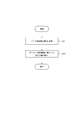
- FIG. 8 is a flowchart illustrating an example of a procedure of controlling the communication device 1 according to an embodiment. Hereinafter, the operation of the communication device 1 according to an embodiment will be described.
- the control unit 62 acquires a period in which data is not transmitted from the communication module 50 (step S11).
- a period in which data is not transmitted from the communication module 50 acquired in step S11 is abbreviated as a "data non-transmission period" as appropriate in the present specification and the drawings.
- the data non-transmission period may be, for example, a period in which data was not actually transmitted from the communication module 50 until now. Further, the data non-transmission period may be, for example, a period from the time of the last transmission of data from the communication module 50 to the current time when the communication module 50 has not transmitted data until now. Furthermore, the data non-transmission period may be, for example, a period during which data is to be transmitted from the communication module 50 when the communication module 50 has a schedule for transmitting data from now. The data non-transmission period may be a period from the time when data was last received from the external device to the current time, when the communication device 1 is connected to the external device via the external terminal. The data non-transmission period may be a period from the last transmission of data to the present time, in the case where the accumulated data is transmitted to a server etc. on condition that the communication device 1 accumulates data by a predetermined amount or more. .
- control unit 62 may determine the non-data transmission period based on the allocation of radio resources for data transmission and the like. Further, in one embodiment, the control unit 62 may determine the data non-transmission period based on, for example, the presence or absence of data to be transmitted stored in the storage unit 61 or the amount of data to be transmitted. In one embodiment, the control unit 62 may determine the non-data transmission period based on, for example, a schedule of data transmission timing notified from a base station or a server.
- Information up to the present of the data non-transmission period may be stored as a history in the storage unit 61 or the like.
- information including the future of the data non-transmission period may be stored in the storage unit 61 or the like, for example, when the control unit 62 and / or the communication module 50 define the data transmission timing.
- the information including the future of the data non-transmission period may be directly grasped by, for example, the control unit 62 and / or the communication module 50 without being stored in the storage unit 61 or the like.
- step S11 the control unit 62 may inquire, for example, the communication module 50 or the storage unit 61 about the data non-transmission period. On the other hand, in step S11, for example, the communication module 50 or the storage unit 61 may periodically notify the control unit 62 of the data non-transmission period.
- control unit 62 When the data non-transmission period is acquired in step S11, the control unit 62 performs control regarding at least one of DRX and PSM based on the acquired data non-transmission period (step S12). In step S12, the control unit 62 may perform various controls on the DRX by the communication module 50 and the PSM of the communication by the communication module 50. Further, in step S12, control relating to either DRX or PSM may be performed, or control relating to both DRX and PSM may be performed.
- the control unit 62 controls at least one of DRX by the communication module 50 and PSM of communication by the communication module 50 based on the data non-transmission period.
- the control relating to DRX may typically be start of DRX, stop, maintenance of started or stopped state of DRX, change of DRX period, change of sleep period in DRX, etc. .
- the control relating to PSM may typically be starting PSM, stopping PSM, maintaining started or stopped state of PSM, changing PSM period, changing sleep period in PSM, etc.
- DRX and PSM typically, DRX may be stopped to start PSM, or PSM may be stopped to start DRX.
- the control unit 62 may perform control related to eDRX by the communication module instead of control related to control related to DRX.
- the control related to at least one of DRX and PSM performed in step S12 can be made various according to the data non-transmission period acquired in step S11.
- the contents of such control may be defined in advance and stored, for example, in the storage unit 61.
- the control unit 62 reads the content of the control associated with the acquired data non-transmission period from the storage unit 61, and performs the control.
- the above-mentioned discontinuous reception (DRX) may be DRX (Discontinuous Reception) defined by 3GPP.
- the above-mentioned extended discontinuous reception (eDRX) may be eDRX (Extended Discontinuous Reception) defined by 3GPP.
- the above-mentioned power saving mode (PSM) may be PSM (Power Saving Mode) defined by 3GPP.
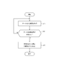
- FIG. 9 is a flowchart illustrating a specific example of an operation performed by the communication device 1 according to an embodiment. Hereinafter, a specific example of the operation of the communication device 1 according to an embodiment will be described.
- step S11 the control unit 62 acquires a data non-transmission period.
- the operation performed in step S11 is performed in the same manner as described in FIG.
- step S11 the control unit 62 determines whether the acquired data non-transmission period is equal to or more than a predetermined one (step S22). In step S22, the control unit 62 determines whether or not the data non-transmission period is equal to or longer than a predetermined time, such as 10 seconds.
- step S22 If it is determined in step S22 that the data non-transmission period is not longer than a predetermined period, the control unit 62 returns to step S11 and continues the process.
- step S22 when it is determined in step S22 that the data non-transmission period is equal to or greater than the predetermined value, the control unit 62 performs the process of step S23.
- step S23 the control unit 62 performs control relating to the DRX and / or PSM corresponding to each in accordance with the result determined in step S22 (step S23).
- the control unit 62 may start DRX. Also, for example, when it is determined that the data non-transmission period is 60 seconds or more, the control unit 62 may stop DRX and start PSM. Also, for example, when it is determined that the data non-transmission period is 20 seconds or more, the control unit 62 may stop the PSM. Also, for example, when it is determined that the data non-transmission period is 10 minutes or more, the control unit 62 may stop PSM and start DRX.
- the storage unit 61 or the like previously stores the data non-transmission period and the control content related to DRX and / or PSM corresponding to each. You may
- FIG. 10 is a flowchart illustrating a specific example of the operation performed by the communication device 1 according to an embodiment. Hereinafter, a specific example of the operation of the communication device 1 according to an embodiment will be described.
- the operation shown in FIG. 10 is to change the operation in step S23 shown in FIG.
- step S23 at least one of DRX and PSM is started or stopped.
- step S33 the operation of step S33 is performed instead of step S23.
- the control unit 62 changes the period of at least one of DRX and PSM.
- the control unit 62 may change the sleep period in at least one of DRX and PSM.
- the control unit 62 may shorten the DRX period from 2 minutes to 1 minute. Also, for example, when it is determined that the data non-transmission period is 10 seconds or more, the control unit 62 may extend the DRX period from 2 minutes to 4 minutes. Also, for example, when it is determined that the data non-transmission period is 1 minute or more, the control unit 62 may extend the PSM period from 5 minutes to 10 minutes. Also, for example, when it is determined that the data non-transmission period is 30 seconds or more, the control unit 62 may shorten the sleep period in DRX from 2.56 seconds to 1 second.
- the control unit 62 may extend the sleep period in eDRX from 10 minutes to 43 minutes. For example, if it is determined that the data non-transmission period is 30 minutes or more, the control unit 62 may extend the sleep period in PSM from 1 hour to 6 hours.
- the sleep period in at least one of DRX and PSM is changed in step S33, not only the sleep period may be extended, but also the sleep period may be shortened.
- the period changed in step S33 may be changed in accordance with the length of the data non-transmission period which is determined in step S22 or more.
- at least one of DRX and PSM may be gradually extended (or shortened) as the data non-transmission period exceeds a plurality of periods set in step S22.
- the sleep period in at least one of DRX and PSM may be gradually extended (or shortened) in stages.
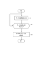
- FIG. 11 is a flowchart illustrating a specific example of an operation performed by the communication device 1 according to an embodiment. Hereinafter, a specific example of the operation of the communication device 1 according to an embodiment will be described.
- the operation shown in FIG. 11 is to change the operation after step S33 shown in FIG.
- step S33 the sleep period in at least one of DRX and PSM is changed.
- step S43 the control unit 62 extends the sleep period in DRX (step S43).
- step S44 determines whether the sleep period is extended to a predetermined period.
- the upper limit period for extending the sleep period in DRX may be defined in advance, for example, 2.56 seconds (10.24 seconds or 43.96 minutes for eDRX). If it is determined in step S44 that the sleep period has not been extended to the predetermined period, the control unit 62 returns to step S11 and continues the process.
- step S44 when it is determined in step S44 that the sleep period has been extended to the predetermined period, the control unit 62 starts PSM (step S45). For example, in step S45, DRX may be stopped at the start of PSM.
- the controller 62 may initiate PSM when sleep in DRX is extended to a predetermined period.
- control related to DRX and / or PSM as described above is performed based on information received from the outside such as a base station or a server.
- control related to DRX and / or PSM is performed based on information from a system different from information received from the outside such as a base station or a server, that is, data non-transmission period. be able to. Therefore, when implemented as an IoT unit, for example, the communication device 1 according to one embodiment can realize flexible use that can not be conventionally achieved.
- the communication device 1 according to one embodiment can reduce power consumption by appropriately controlling DRX and / or PSM in such flexible use. As a result, the convenience of the communication device 1 and the communication module 50 can be improved.
- 12A to 12D are diagrams showing an example of the operation of the communication device 1 according to an embodiment.
- 12A to 12D show an example of the operation of the communication device 1 described in FIG.
- the communication device 1 when there is no data to be transmitted as shown in FIG. 12A, DRX is started as shown in FIG. 12B. Thus, the communication device 1 can reduce power consumption. Also, in the communication device 1 according to an embodiment, when there is no data to be further transmitted in DRX as shown in FIG. 12C, the sleep period in DRX is extended to the upper limit (step S43). Therefore, the communication device 1 can further reduce power consumption. In addition, when the sleep period in the DRX is extended to the upper limit (step S44), the communication device 1 according to an embodiment starts PSM as illustrated in FIG. 12D. Therefore, the communication device 1 can further reduce power consumption.
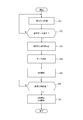
- FIG. 13 is a flowchart illustrating a specific example of an operation performed by the communication device 1 according to an embodiment. Hereinafter, a specific example of the operation of the communication device 1 according to an embodiment will be described.
- control unit 62 first starts DRX or PSM (step S51).
- step S51 When starting DRX or PSM in step S51, for example, it may start as described in FIG. 9 or FIG.
- step S52 determines whether data to be transmitted from the communication module 50 is generated (step S52).
- step S52 determines whether data to be transmitted from the communication module 50 is generated, for example, acquisition of a data non-transmission period in step S11 of FIG. 8 can be performed. For example, when determining whether there is data to be transmitted, a period during which data is not transmitted may be acquired. If it is determined in step S52 that no data to be transmitted is generated, the control unit 62 returns to step S51 and continues the process.
- control unit 62 may stop the started DRX or PSM (step S53) and transmit data from the communication module 50 (step S54). ).
- the control unit 62 may start DRX (step S55).
- the control unit 62 determines whether a predetermined period has elapsed (step S56).
- the control unit 62 may stop DRX and start PSM after a predetermined period has elapsed (step S57).
- the control unit 62 may stop the DRX or PSM and control the communication module 50 to transmit data.
- the control unit 62 may start DRX.
- the control unit 62 may continue the started DRX until a predetermined period has elapsed since the data was transmitted from the communication module 50.
- the control unit 62 may stop the started DRX and start the PSM when a predetermined period has elapsed since the data was transmitted from the communication module 50.
- power consumption can be reduced while performing appropriate tracking as desired.
- each functional unit can be rearranged so as not to be logically contradictory.
- a plurality of functional units may be combined or divided into one.
- Each embodiment according to the present disclosure described above is not limited to be implemented faithfully to each described embodiment, and may be implemented by combining the respective features or omitting some of them as appropriate. .
- the communication device 1 includes the communication module 50 that can be, for example, an IoT module, and the control unit 62 controls the communication module 50.
- the communication device 1 can be realized, for example, with an IoT unit.
- the communication module 50 may include a control unit configured by a processor such as a CPU and a storage unit configured by a memory, for example. In this case, the communication module 50 can perform control alone. That is, in one embodiment, the communication module 50 may be mountable to the communication device 1.
- the communication module 50 performs control regarding at least one of intermittent reception (DRX) by the communication module 50 and power saving mode (PSM) of communication by the communication module 50 based on a period during which data is not transmitted from the communication module 50. .
- DRX intermittent reception
- PSM power saving mode
- the embodiments described above are not limited to the implementation as a communication device and communication module.
- the embodiments described above may be implemented as a communication method of a communication apparatus and a program that is executed by a controller that controls the communication apparatus.
Abstract
This device is equipped with communication equipment and a controller for controlling communication by the communication equipment. The controller performs control pertaining to at least either discontinuous reception (DRX) by the communication equipment or power saving mode (PSM) for communication by the communication equipment on the basis of periods in which data is not transmitted from the communication equipment.
Description
本出願は、2017年12月26日に日本国に特許出願された特願2017-250172の優先権を主張するものであり、この先の出願の開示全体を、ここに参照のために取り込む。
This application claims the priority of Japanese Patent Application No. 2017-250172 filed in Japan on Dec. 26, 2017, the entire disclosure of the prior application is incorporated herein by reference.
本開示は、装置、通信機器、及び通信方法に関する。
The present disclosure relates to an apparatus, a communication device, and a communication method.
従来、測定装置によって測定したデータを、サーバに収集するシステムが知られている。例えば、特許文献1は、測定装置が測定したデータを、端末によってサーバに送信するシステムを開示している。
Conventionally, a system is known which collects data measured by a measuring device on a server. For example, Patent Document 1 discloses a system in which data measured by a measurement device is transmitted by a terminal to a server.
一実施形態に係る装置は、通信機器と、前記通信機器の通信を制御するコントローラと、を備える。
前記コントローラは、前記通信機器からデータを送信しない期間に基づいて、前記通信機器による間欠受信(DRX)及び前記通信機器による通信の省電力モード(PSM)の少なくとも一方に関する制御を行う。 An apparatus according to an embodiment includes a communication device and a controller that controls communication of the communication device.
The controller performs control related to at least one of intermittent reception (DRX) by the communication device and a power saving mode (PSM) of communication by the communication device based on a period in which data is not transmitted from the communication device.
一実施形態に係る通信機器は、装置に搭載可能な通信機器である。
前記通信機器は、前記通信機器からデータを送信しない期間に基づいて、前記通信機器による間欠受信(DRX)及び前記通信機器による通信の省電力モード(PSM)の少なくとも一方に関する制御を行う。 The communication device according to one embodiment is a communication device that can be installed in a device.
The communication device performs control regarding at least one of intermittent reception (DRX) by the communication device and a power saving mode (PSM) of communication by the communication device based on a period in which data is not transmitted from the communication device.
一実施形態に係る通信方法は、通信機器の通信を制御する制御ステップを含む装置の通信方法である。前記通信方法は、前記制御ステップにおいて、前記通信機器からデータを送信しない期間に基づいて、前記通信機器による間欠受信(DRX)及び前記通信機器による通信の省電力モード(PSM)の少なくとも一方に関する制御を行う。
A communication method according to an embodiment is a device communication method including a control step of controlling communication of a communication device. In the communication method, in the control step, control relating to at least one of intermittent reception (DRX) by the communication device and a power saving mode (PSM) of communication by the communication device based on a period during which data is not transmitted from the communication device. I do.
従来のシステムでは、例えばモノのインターネット(Internet of Things(IoT))技術の普及などに伴い、利便性の向上が求められている。本開示は、利便性の高い通信装置、通信モジュール、通信方法、及びプログラムを提供することに関する。一実施形態によれば、利便性の高い通信装置、通信モジュール、通信方法、及びプログラムを提供することができる。以下、本開示の一実施形態が、図面を参照して説明される。一実施形態に係る通信装置1(図1参照)は、典型的にはIoT(Internet of Things)向けの通信装置1であってよい。一実施形態に係る通信装置1は、IoT向けの通信装置1に限定されず、無線通信機能を有する各種の通信装置1であってよい。
In the conventional system, for example, with the spread of Internet of Things (IoT) technology, improvement of convenience is required. The present disclosure relates to providing a highly convenient communication device, communication module, communication method, and program. According to one embodiment, a highly convenient communication device, communication module, communication method, and program can be provided. Hereinafter, an embodiment of the present disclosure will be described with reference to the drawings. The communication device 1 according to one embodiment (see FIG. 1) may be the communication device 1 for Internet of Things (IoT). The communication device 1 according to an embodiment is not limited to the communication device 1 for IoT, and may be various communication devices 1 having a wireless communication function.
通信装置1は、外部のサーバ等の外部機器と通信してよい。通信装置1は、外部環境の情報を取得してよい。通信装置1は、取得した外部環境の情報を、外部のサーバ等に送信してよい。通信装置1は、他の機器又は商品若しくは貨物等に取り付けられた状態で使用されてよい。通信装置1は、小型化されることによって、他の機器又は商品若しくは貨物等に取り付けられやすくなる。
The communication device 1 may communicate with an external device such as an external server. The communication device 1 may acquire information on the external environment. The communication device 1 may transmit the acquired external environment information to an external server or the like. The communication device 1 may be used in a state of being attached to another device or a product or a cargo. As the communication device 1 is miniaturized, it becomes easy to be attached to another device, goods, cargo or the like.
図1及び図2に示されるように、一実施形態に係る通信装置1は、筐体10と、内部構造13とを備えてよい。内部構造13は、筐体10の内部に位置してよい。
As shown in FIG. 1 and FIG. 2, the communication device 1 according to one embodiment may include a housing 10 and an internal structure 13. The internal structure 13 may be located inside the housing 10.
筐体10は、プレート11と、ケース12とを備えてよい。筐体10は、内部構造13を保護しうる。筐体10は、プレート11とケース12との間に、封止のためのパッキンをさらに備えてよい。プレート11とケース12との間がパッキンで封止されることによって、筐体10の内部に水分又は塵等が侵入しにくくなる。結果として、内部構造13が水分又は塵等から保護されやすくなる。
The housing 10 may include a plate 11 and a case 12. The housing 10 can protect the internal structure 13. The housing 10 may further include a packing for sealing between the plate 11 and the case 12. By sealing the space between the plate 11 and the case 12 with packing, moisture, dust and the like are less likely to intrude into the inside of the housing 10. As a result, the internal structure 13 is easily protected from moisture or dust.
筐体10の外観形状は、互いに交差するX軸、Y軸、及びZ軸それぞれにほぼ沿う辺を有する直方体状であってよい。X軸、Y軸、及びZ軸は、互いに直交してよい。筐体10のX軸方向の長さは、筐体10のY軸方向の長さ、及び、筐体10のZ軸方向の長さより長いものとする。筐体10のY軸方向の長さは、筐体10のZ軸方向の長さより長いものとする。X軸方向は、第1方向ともいう。Y軸方向は、第2方向ともいう。Z軸方向は、第3方向ともいう。言い換えれば、筐体10の第1方向の長さは、第2方向の長さ及び第3方向の長さより長い。第1方向、第2方向、及び第3方向はそれぞれ、筐体10の長手方向、短手方向、及び厚み方向ともいう。
The external shape of the housing 10 may be a rectangular parallelepiped having sides substantially along the X axis, the Y axis, and the Z axis which intersect with each other. The X, Y and Z axes may be orthogonal to one another. The length in the X-axis direction of the housing 10 is longer than the length in the Y-axis direction of the housing 10 and the length in the Z-axis direction of the housing 10. The length in the Y-axis direction of the housing 10 is longer than the length in the Z-axis direction of the housing 10. The X-axis direction is also referred to as a first direction. The Y-axis direction is also referred to as a second direction. The Z-axis direction is also referred to as a third direction. In other words, the length in the first direction of the housing 10 is longer than the length in the second direction and the length in the third direction. The first direction, the second direction, and the third direction are also referred to as the longitudinal direction, the short direction, and the thickness direction of the housing 10, respectively.
筐体10は、通信装置1の用途に応じた使用環境に耐え得る強度を有する材料で構成されてよい。例えば、筐体10は、樹脂又は金属等で構成されてよい。
The housing 10 may be made of a material having a strength that can withstand the use environment according to the application of the communication device 1. For example, the housing 10 may be made of resin or metal.
プレート11は、スイッチハンドル11Aと、報知窓11Bとを有してよい。スイッチハンドル11Aは、内部構造13に含まれるスイッチ81(図3参照)に対応して配置される。このようにすることで、ユーザは、スイッチハンドル11Aを介してスイッチ81を操作しうる。スイッチハンドル11Aは、可撓性を有する材料で構成されてよい。報知窓11Bは、内部構造13に含まれる報知部80(図3参照)に対応して配置される。報知窓11Bは、透明部材等で構成されてよい。このようにすることで、ユーザは、報知窓11Bを介して報知部80を視認しうる。
The plate 11 may have a switch handle 11A and a notification window 11B. The switch handle 11A is disposed corresponding to the switch 81 (see FIG. 3) included in the internal structure 13. By doing this, the user can operate the switch 81 via the switch handle 11A. The switch handle 11A may be made of a flexible material. The notification window 11B is arranged corresponding to the notification unit 80 (see FIG. 3) included in the internal structure 13. The notification window 11B may be made of a transparent member or the like. By doing this, the user can visually recognize the notification unit 80 through the notification window 11B.
プレート11は、孔11C、孔11D、孔11E及び孔11Fをさらに有してよい。孔11Cは、内部構造13に含まれる気圧センサ71(図3参照)に対応して配置される。孔11Dは、内部構造13に含まれる温度センサ72(図3参照)に対応して配置される。孔11Eは、内部構造13に含まれる湿度センサ73(図3参照)に対応して配置される。孔11Fは、内部構造13に含まれる照度センサ74(図3参照)に対応して配置される。気圧センサ71、温度センサ72、湿度センサ73及び照度センサ74は、センサ70(図3参照)と総称される。各センサ70は、筐体10の外部の環境を高い精度で検出しうる。
The plate 11 may further have a hole 11C, a hole 11D, a hole 11E and a hole 11F. 11 C of holes are arrange | positioned corresponding to the air pressure sensor 71 (refer FIG. 3) contained in the internal structure 13. As shown in FIG. The holes 11D are arranged corresponding to the temperature sensor 72 (see FIG. 3) included in the internal structure 13. The holes 11E are disposed corresponding to the humidity sensor 73 (see FIG. 3) included in the internal structure 13. The holes 11F are arranged corresponding to the illuminance sensor 74 (see FIG. 3) included in the internal structure 13. The atmospheric pressure sensor 71, the temperature sensor 72, the humidity sensor 73, and the illuminance sensor 74 are collectively referred to as a sensor 70 (see FIG. 3). Each sensor 70 can detect the environment outside the housing 10 with high accuracy.
ケース12は、底面部12Aと、側面部12Bとを有してよい。底面部12Aは、内部構造13を挟んでプレート11の反対側に位置する。側面部12Bは、プレート11と底面部12Aとの間に位置し、底面部12A及びプレート11に交差する。ケース12は、側面部12Bに、差込口12C、12D及び12Eを有してよい。差込口12C及び12Dは、内部構造13に含まれる外部端子22及び23(図3参照)に対応して配置されてよい。このようにすることで、外部機器の端子は、差込口12C及び12Dを介して、外部端子22及び23と接続しうる。差込口12Eは、内部構造に含まれるスロット24(図3参照)に対応して配置される。このようにすることで、SIM(Subscriber Identity Module)カード等が、差込口12Eを介して、スロット24に挿入されうる。
The case 12 may have a bottom 12A and a side 12B. The bottom portion 12A is located on the opposite side of the plate 11 with the internal structure 13 interposed therebetween. The side surface portion 12B is located between the plate 11 and the bottom surface portion 12A, and intersects the bottom surface portion 12A and the plate 11. The case 12 may have insertion ports 12C, 12D and 12E in the side surface portion 12B. The insertion ports 12C and 12D may be disposed corresponding to the external terminals 22 and 23 (see FIG. 3) included in the internal structure 13. By doing this, the terminals of the external device can be connected to the external terminals 22 and 23 through the insertion ports 12C and 12D. The insertion port 12E is disposed corresponding to the slot 24 (see FIG. 3) included in the internal structure. By doing this, a SIM (Subscriber Identity Module) card or the like can be inserted into the slot 24 through the insertion port 12E.
孔11C~11F及び報知窓11Bの少なくとも1つは、ケース12の側面部12Bに配置されてもよい。
At least one of the holes 11C to 11F and the notification window 11B may be disposed on the side surface 12B of the case 12.
プレート11は、マーク11Gをさらに有してよい。マーク11Gは、例えば通信装置1の製造主体を表すロゴマーク等であってよい。ユーザは、マーク11Gの位置に基づいて、通信装置1の向きを特定しうる。ユーザは、例えば通信装置1を地面等に配置する場合、プレート11の側が地面等に接触しないように通信装置1を配置しうる。つまり、ユーザは、ケース12の底面部12Aの側が地面等に接触するように通信装置1を配置しうる。プレート11の側が地面等に接触しないことによって、孔11C~11F及び報知窓11Bが地面等でふさがれにくくなる。孔11C~11F及び報知窓11Bがケース12の側面部12Bに配置される場合、ケース12の底面部12Aの側が地面等に接触するように通信装置1が配置されることによって、孔11C~11F及び報知窓11Bが地面等でふさがれにくくなる。
The plate 11 may further have marks 11G. The mark 11 </ b> G may be, for example, a logo mark or the like representing a main body of the communication device 1. The user can specify the orientation of the communication device 1 based on the position of the mark 11G. For example, when disposing the communication device 1 on the ground or the like, the user may arrange the communication device 1 so that the side of the plate 11 does not contact the ground or the like. That is, the user can arrange the communication device 1 such that the bottom surface 12A of the case 12 contacts the ground or the like. When the side of the plate 11 is not in contact with the ground or the like, the holes 11C to 11F and the notification window 11B are less likely to be blocked by the ground or the like. When the holes 11C to 11F and the notification window 11B are disposed on the side surface portion 12B of the case 12, the communication device 1 is disposed such that the bottom surface portion 12A of the case 12 contacts the ground or the like. And notification window 11B becomes difficult to be closed by the ground etc.
図3に示されるように、内部構造13は、アンテナ100と、通信モジュール50とを含む。内部構造13は、外部端子22をさらに含んでよい。内部構造13は、図4に示されるように、回路基板20をさらに含んでよい。内部構造13は、バッテリ30をさらに含んでよい。内部構造13は、フレーム40をさらに含んでよい。内部構造13は、センサ70と、報知部80と、スイッチ81とをさらに含んでよい。
As shown in FIG. 3, the internal structure 13 includes an antenna 100 and a communication module 50. The internal structure 13 may further include an external terminal 22. The internal structure 13 may further include a circuit board 20, as shown in FIG. Internal structure 13 may further include a battery 30. Internal structure 13 may further include a frame 40. The internal structure 13 may further include a sensor 70, a notification unit 80, and a switch 81.
図3に示されるように、アンテナ100は、筐体10において、X軸の正の方向の側に位置してよい。通信モジュール50及び外部端子22の少なくとも一方は、筐体10において、X軸の負の方向の側に位置してよい。つまり、アンテナ100は、筐体10の第1方向の一端の側に位置してよい。通信モジュール50及び外部端子22の少なくとも一方は、筐体10の第1方向の他端の側に位置してよい。アンテナ100と、通信モジュール50及び外部端子22の少なくとも一方とは、第1方向に沿って、互いに反対側に位置してよい。このようにすることで、アンテナ100は、電波のノイズ源となりうる通信モジュール50及び外部端子22の少なくとも一方から所定距離より遠くに離されることによって、電波を受信する際に、ノイズ源による影響を受けにくくなる。結果として、通信装置1の利便性が高められうる。多くの場合にスマートフォンなどの携帯電話よりも小型化が要請されノイズ源による影響が懸念されるIoT向けの通信装置1においては、より効果的である。外部端子22が複数設けられる場合、少なくとも一つの外部端子22が、第1方向に沿って、アンテナ100と反対側に位置していれば、ノイズ源による影響を低減する効果が得られる。
As shown in FIG. 3, the antenna 100 may be located on the side of the housing 10 in the positive direction of the X axis. At least one of the communication module 50 and the external terminal 22 may be located on the negative side of the X axis in the housing 10. That is, the antenna 100 may be located on one end side of the housing 10 in the first direction. At least one of the communication module 50 and the external terminal 22 may be located on the other side of the housing 10 in the first direction. The antenna 100 and at least one of the communication module 50 and the external terminal 22 may be located opposite to each other along the first direction. By doing this, the antenna 100 is separated from the predetermined distance from at least one of the communication module 50 and the external terminal 22 which can be noise sources of radio waves, thereby receiving the influence of the noise sources when radio waves are received. It becomes difficult to receive. As a result, the convenience of the communication device 1 can be enhanced. It is more effective in the communication apparatus 1 for IoT, which is required to be smaller in size than a mobile phone such as a smartphone in many cases and is concerned about the influence of noise sources. When a plurality of external terminals 22 are provided, if at least one external terminal 22 is located on the opposite side to the antenna 100 along the first direction, an effect of reducing the influence of noise sources can be obtained.
回路基板20は、板状であってよい。回路基板20は、XY平面に沿って位置してよい。回路基板20は、樹脂又はセラミック等の材料で構成されてよい。回路基板20には、各種部品が実装されてよい。回路基板20に実装される部品は、例えば、電子部品60(図5参照)、センサ70、又は報知部80等を含んでよい。回路基板20には、端子又は配線等が実装されてもよい。
The circuit board 20 may be plate-shaped. The circuit board 20 may be located along the XY plane. The circuit board 20 may be made of a material such as resin or ceramic. Various components may be mounted on the circuit board 20. The components mounted on the circuit board 20 may include, for example, an electronic component 60 (see FIG. 5), a sensor 70, or a notification unit 80 or the like. Terminals or wires may be mounted on the circuit board 20.
図4に示されるように、回路基板20のZ軸の負の方向の側の面には、バッテリ端子21と、外部端子22とが実装されてよい。
As shown in FIG. 4, the battery terminal 21 and the external terminal 22 may be mounted on the surface of the circuit board 20 on the negative direction side of the Z axis.
バッテリ端子21は、バッテリ30の正極に接続されるバッテリ端子21Aと、バッテリ30の残量を検出するためのバッテリ端子21Bと、バッテリ30の負極に接続されるバッテリ端子21Cとを含む。バッテリ端子21は、バッテリ30を付勢する付勢機構を有してよい。バッテリ端子21は、バッテリ30をX軸の負の方向に付勢してよい。
Battery terminal 21 includes a battery terminal 21A connected to the positive terminal of battery 30, a battery terminal 21B for detecting the remaining amount of battery 30, and a battery terminal 21C connected to the negative terminal of battery 30. The battery terminal 21 may have a biasing mechanism that biases the battery 30. The battery terminal 21 may bias the battery 30 in the negative direction of the X axis.
外部端子22は、支持部22Aによって回路基板20に固定される。外部端子22は、外部機器を接続可能な端子である。外部端子22は、例えば、マイクロUSB(Universal Serial Bus)のコネクタを接続可能な端子であってよい。通信装置1は、外部端子22を介して接続された外部機器によって、制御されてよい。通信装置1は、外部端子22から供給される電力によって、バッテリ30を充電してもよい。通信装置1は、バッテリ30の電力が不足する場合、又はバッテリ30を備えない場合に、外部端子22から供給される電力によって動作してもよい。
The external terminal 22 is fixed to the circuit board 20 by the support 22A. The external terminal 22 is a terminal to which an external device can be connected. The external terminal 22 may be, for example, a terminal to which a micro USB (Universal Serial Bus) connector can be connected. The communication device 1 may be controlled by an external device connected via the external terminal 22. The communication device 1 may charge the battery 30 with the power supplied from the external terminal 22. The communication device 1 may operate by the power supplied from the external terminal 22 when the power of the battery 30 is insufficient or when the battery 30 is not provided.
外部端子23は、信号を変換する回路の一種であるUART(Universal Asynchronous Receiver/Transmitter)に対応する端子であってよい。UARTに対応する端子は、例えば、通信装置1の外部に設けられているセンサと接続するために用いられうる。このセンサは、内部構造13に含まれるセンサ70とは別に設けられたセンサとしてよい。
The external terminal 23 may be a terminal corresponding to a universal asynchronous receiver / transmitter (UART) which is a type of circuit for converting a signal. A terminal corresponding to the UART can be used, for example, to connect to a sensor provided outside the communication device 1. This sensor may be a sensor provided separately from the sensor 70 included in the internal structure 13.
スロット24は、例えば、SIMカードが挿入されてよい。スロット24は、メモリカード等の他のカードが挿入されてもよい。
For example, a SIM card may be inserted into the slot 24. The slot 24 may be inserted with another card such as a memory card.
バッテリ30は、通信装置1の各構成部に電力を供給してよい。バッテリ30は、充電可能な二次電池を含んでよい。二次電池は、例えば、リチウムイオン電池、ニッケルカドミウム電池、又はニッケル水素電池等を含んでよい。バッテリ30は、二次電池に限られず、充電できない一次電池を含んでよい。一次電池は、例えば、アルカリ電池又はマンガン電池等を含んでよい。
The battery 30 may supply power to each component of the communication device 1. The battery 30 may include a rechargeable secondary battery. The secondary battery may include, for example, a lithium ion battery, a nickel cadmium battery, or a nickel hydrogen battery. The battery 30 is not limited to a secondary battery, and may include a primary battery that can not be charged. The primary battery may include, for example, an alkaline battery or a manganese battery.
フレーム40(図3参照)は、図4に示されるように、回路基板20及びバッテリ30を保持してよい。フレーム40は、その内部に回路基板20及びバッテリ30を収容してもよい。回路基板20とバッテリ30とフレーム40とは、一体化されてよい。回路基板20とバッテリ30とフレーム40とが一体化されることで、内部構造13の強度が高められうる。
The frame 40 (see FIG. 3) may hold the circuit board 20 and the battery 30, as shown in FIG. The frame 40 may house the circuit board 20 and the battery 30 therein. The circuit board 20, the battery 30, and the frame 40 may be integrated. By integrating the circuit board 20, the battery 30, and the frame 40, the strength of the internal structure 13 can be enhanced.
図3に示されるように、フレーム40は、本体41を有してよい。本体41は、平面部41Aと、側面部41Bとを有してよい。平面部41Aは、Z軸の正の方向の側に位置してよい。平面部41Aは、XY平面に沿って広がる板状であってよい。側面部41Bは、平面部41Aの周囲からZ軸の負の方向の側に突出してよい。本体41は、側面部41Bによって囲まれる開口をZ軸の負の方向の側に有するといえる。本体41は、開口の側から回路基板20及びバッテリ30を収容してよい。
As shown in FIG. 3, the frame 40 may have a body 41. The main body 41 may have a flat surface portion 41A and a side surface portion 41B. The flat portion 41A may be located on the positive side of the Z axis. The flat portion 41A may be in the form of a plate extending along the XY plane. The side surface portion 41B may protrude from the periphery of the flat surface portion 41A in the negative direction of the Z axis. It can be said that the main body 41 has an opening surrounded by the side surface portion 41B on the side in the negative direction of the Z axis. The main body 41 may accommodate the circuit board 20 and the battery 30 from the side of the opening.
図4に示されるように、フレーム40は、保持部42A及び42Bと、凸部45A及び45Bとを有してよい。
As shown in FIG. 4, the frame 40 may have holding portions 42A and 42B and convex portions 45A and 45B.
保持部42A及び42Bは、バッテリ30のX軸の正の方向の側に位置する2つの角に合わせて位置してよい。保持部42A及び42Bは、本体41の側面部41Bから、Z軸の負の方向の側にさらに突出してよい。Y軸方向から見た保持部42A及び42Bの形状は、L字状であってよい。保持部42A及び42Bの先端は、バッテリ30をZ軸の負の方向の側で保持するように、X軸の負の方向の側に突出してよい。Y軸方向から見た保持部42A及び42Bの形状は、L字状に限られず、バッテリ30を保持しうる任意の形状であってよい。
The holding portions 42A and 42B may be positioned at two corners located on the positive direction side of the X axis of the battery 30. The holding portions 42A and 42B may further protrude from the side surface portion 41B of the main body 41 to the side in the negative direction of the Z axis. The shape of the holding portions 42A and 42B viewed from the Y-axis direction may be L-shaped. The tips of the holding portions 42A and 42B may project in the negative direction side of the X axis so as to hold the battery 30 on the negative direction side of the Z axis. The shape of the holding portions 42A and 42B viewed from the Y-axis direction is not limited to the L shape, and may be any shape that can hold the battery 30.
凸部45A及び45Bは、バッテリ30のX軸の負の方向の側に位置する2つの角に合わせて位置してよい。凸部45A及び45Bは、本体41の側面部41Bから、Z軸の負の方向の側にさらに突出してよい。凸部45A及び45Bは、例えばバッテリ30にX軸の正の方向から力が加えられたとき、バッテリ30のX軸の負の方向の側の端部と当接しうる。このようにすることで、バッテリ30がX軸の負の方向に動いても支持部22Aに衝突しにくくなる。結果として、支持部22Aに対する衝撃が低減されうる。
The convex portions 45A and 45B may be positioned at two corners located on the negative side of the X axis of the battery 30. The protrusions 45A and 45B may further protrude from the side surface portion 41B of the main body 41 to the side in the negative direction of the Z axis. The protrusions 45A and 45B can abut on the end of the battery 30 on the negative direction side of the X axis when, for example, a force is applied to the battery 30 from the positive direction of the X axis. By doing this, even if the battery 30 moves in the negative direction of the X axis, it becomes difficult to collide with the support 22A. As a result, the impact on the support 22A can be reduced.
凸部45A及び45Bは、バッテリ端子21が付勢機構を有する場合、X軸の負の方向に付勢されるバッテリ30を支持してよい。バッテリ30は、バッテリ端子21と凸部45A及び45Bとの間で挟持されてよい。
The protrusions 45A and 45B may support the battery 30 biased in the negative direction of the X axis when the battery terminal 21 has a biasing mechanism. The battery 30 may be sandwiched between the battery terminal 21 and the protrusions 45A and 45B.
図3に示されるように、フレーム40は、フレーム開口46を有してよい。フレーム開口46は、本体41の板状部材の一部に位置する開口であってよい。フレーム開口46は、通信モジュール50が実装されている位置に対応して位置してよい。
As shown in FIG. 3, the frame 40 may have a frame opening 46. The frame opening 46 may be an opening located in a part of the plate-like member of the main body 41. The frame opening 46 may be located corresponding to the position where the communication module 50 is mounted.
フレーム40の各構成部は、例えば、適切な強度の材料を含んでよい。適切な強度の材料は、例えば、樹脂又は金属等を含んでよい。フレーム40の各構成部は、適切な強度の素材で一体として形成されてよい。フレーム40の各構成部が一体として形成されることで、フレーム40の強度が高められうる。結果として、内部構造13に対して外部からの衝撃が伝達しにくくなる。
Each component of the frame 40 may, for example, comprise a material of appropriate strength. Materials of suitable strength may include, for example, resins or metals. Each component of the frame 40 may be integrally formed of a material of appropriate strength. By integrally forming the components of the frame 40, the strength of the frame 40 can be enhanced. As a result, it is difficult to transmit an external impact to the internal structure 13.
通信モジュール50は、図3に示されるように、回路基板20のZ軸の正の方向の側の面において、フレーム40のフレーム開口46に対応する位置に実装されてよい。通信モジュール50は、回路基板20の方に延びる側壁部50Aを含んでよい。側壁部50Aは、シールドケースであってよいし、他の部材であってもよい。側壁部50Aは、内部構造13に対してZ軸の正の方向から加えられる力を受けうる。このようにすることで、通信モジュール50に加わる力が低減されうる。結果として、通信モジュール50が変形しにくくなる。
The communication module 50 may be mounted at a position corresponding to the frame opening 46 of the frame 40 on the surface on the positive direction side of the Z axis of the circuit board 20, as shown in FIG. The communication module 50 may include a side wall portion 50A extending toward the circuit board 20. The side wall portion 50A may be a shield case or may be another member. The side wall portion 50A can receive a force applied to the internal structure 13 from the positive direction of the Z axis. By doing this, the force applied to the communication module 50 can be reduced. As a result, the communication module 50 is less likely to be deformed.
図5に示されるように、通信モジュール50は、回路基板20とは異なる通信回路基板51を介して、回路基板20のZ軸の正の方向の側の面に実装されてよい。通信回路基板51は、例えば、セラミック等の材料で構成されてよい。通信回路基板51は、板状であってよい。通信回路基板51と、バッテリ30のZ軸の正の方向の側の面の少なくとも一部とは、回路基板20を挟んで対向してよい。通信回路基板51と回路基板20とが異なる材料を含む場合、外力による通信回路基板51及び回路基板20それぞれの撓み量は異なりうる。通信回路基板51と、バッテリ30のZ軸の正の方向の側の面の少なくとも一部とが回路基板20を挟んで対向することによって、回路基板20及び通信回路基板51が撓みにくくなる。結果として、通信回路基板51が回路基板20から剥がれにくくなる。
As shown in FIG. 5, the communication module 50 may be mounted on the surface of the circuit board 20 on the positive direction side of the Z axis via the communication circuit board 51 different from the circuit board 20. The communication circuit board 51 may be made of, for example, a material such as ceramic. The communication circuit board 51 may be plate-shaped. The communication circuit board 51 and at least a part of the surface on the positive direction side of the Z axis of the battery 30 may be opposed to each other with the circuit board 20 interposed therebetween. When the communication circuit board 51 and the circuit board 20 contain different materials, the amount of bending of the communication circuit board 51 and the circuit board 20 due to an external force may be different. When the communication circuit board 51 and at least a part of the surface on the positive direction side of the Z axis of the battery 30 face each other with the circuit board 20 interposed therebetween, the circuit board 20 and the communication circuit board 51 are less likely to be bent. As a result, the communication circuit board 51 is less likely to come off the circuit board 20.
通信回路基板51は、回路基板20と対向する側にキャビティ52を有してよい。キャビティ52の内部には、電子部品60の一部が実装されてよい。キャビティ52の内部に実装される電子部品60の一部は、通信に関連しない部品であってよい。電子部品60は、例えば、記憶部61及び制御部62を含む。キャビティ52の内部には、記憶部61及び制御部62が実装されてよい。通信装置1が通信モジュール50を備えない場合、電子部品60は、通信部等を含んでよい。電子部品60は、回路基板20上に実装されてもよいし、通信回路基板51におけるキャビティ52を形成する面に実装されてもよい。 電子部品60がキャビティ52に実装されることによって、電子部品60と回路基板20との間に隙間が形成されうる。このようにすることで、回路基板20の変形に起因する衝撃が電子部品60に伝達しにくくなる。結果として、電子部品60が保護されうる。
The communication circuit board 51 may have a cavity 52 on the side facing the circuit board 20. A part of the electronic component 60 may be mounted inside the cavity 52. A portion of the electronic component 60 mounted inside the cavity 52 may be a component not related to communication. The electronic component 60 includes, for example, a storage unit 61 and a control unit 62. The storage unit 61 and the control unit 62 may be mounted inside the cavity 52. When the communication device 1 does not include the communication module 50, the electronic component 60 may include a communication unit or the like. The electronic component 60 may be mounted on the circuit board 20 or may be mounted on the surface of the communication circuit board 51 on which the cavity 52 is formed. By mounting the electronic component 60 in the cavity 52, a gap can be formed between the electronic component 60 and the circuit board 20. By doing this, it is difficult to transmit the shock resulting from the deformation of the circuit board 20 to the electronic component 60. As a result, the electronic component 60 can be protected.
キャビティ52とバッテリ30のZ軸の正の方向の側の面の少なくとも一部とは、回路基板20を挟んで対向してよい。このようにすることで、外力は、高い剛性を有するバッテリ30によって吸収されやすくなり、通信回路基板51に伝達しにくくなる。結果として、通信回路基板51の変形が低減されうるとともに、キャビティ52内の電子部品60が破損しにくくなる。
The cavity 52 and at least a part of the surface on the positive direction side of the Z axis of the battery 30 may be opposed to each other with the circuit board 20 interposed therebetween. By doing this, the external force is easily absorbed by the battery 30 having high rigidity, and becomes difficult to be transmitted to the communication circuit board 51. As a result, deformation of the communication circuit board 51 can be reduced, and the electronic component 60 in the cavity 52 is less likely to be damaged.
センサ70は、外部環境の情報を取得するために、例えば、気圧センサ71、温度センサ72、湿度センサ73、及び照度センサ74の少なくとも1つを含んでよい。センサ70は、センサ70自身の位置、動き、及び姿勢の少なくとも1つに関する情報を取得するために、例えば、加速度センサ、角速度センサ、及び地磁気センサの少なくとも1つを含んでよい。角速度センサは、センサ70が設けられている機器等の角速度を検出しうる。加速度センサは、センサ70が設けられている機器等に生じている加速度を検出しうる。地磁気センサは、地磁気の向きを検出しうる。センサ70は、位置センサを含んでよい。位置センサは、RFID(Radio Frequency Identifier)、IEEE802.11、Bluetooth(登録商標)等の近距離無線通信の電波等の検出結果に基づいて、センサ70が設けられている機器等の位置情報を検出してよい。このように、センサ70は、通信装置1の状況に関する情報を検出してよい。また、センサ70は、IoT機器に使用されるセンサを少なくとも1つ含んでよい。
The sensor 70 may include, for example, at least one of an atmospheric pressure sensor 71, a temperature sensor 72, a humidity sensor 73, and an illuminance sensor 74 in order to obtain information on the external environment. The sensor 70 may include, for example, at least one of an acceleration sensor, an angular velocity sensor, and a geomagnetic sensor, in order to obtain information on at least one of the position, movement, and attitude of the sensor 70 itself. The angular velocity sensor can detect the angular velocity of the device or the like in which the sensor 70 is provided. The acceleration sensor can detect an acceleration occurring in a device or the like in which the sensor 70 is provided. The geomagnetic sensor can detect the direction of geomagnetism. The sensor 70 may include a position sensor. The position sensor detects position information of a device or the like provided with the sensor 70 based on detection results of radio waves of near field communication such as RFID (Radio Frequency Identifier), IEEE 802.11, Bluetooth (registered trademark), etc. You may Thus, the sensor 70 may detect information regarding the status of the communication device 1. Also, the sensor 70 may include at least one sensor used for the IoT device.
一実施形態において、センサ70に含まれるのは、加速度センサ、角速度センサ、及び地磁気センサに限定されない。一実施形態において、センサ70は、例えば、通信装置1の周囲の温度を検出する温度センサ、通信装置1の周囲の湿度を検出する湿度センサ、及び通信装置1の所定部位における光の照度を検出する照度センサの少なくともいずれかを含んでよい。一実施形態において、センサ70は、前述したセンサ以外の他のセンサを含んでもよい。また、センサ70は、通信装置1に内蔵されるものに限定されず、通信装置1に接続される外部機器に備えられてもよい。この場合、外部機器に備えられるセンサ70は、外部端子23を介して、通信装置1に接続されてよい。一実施形態において、通信モジュール50は、センサ70によって検出されたデータを、サーバ又は他の機器などに送信する。この場合、通信装置1は、適宜、基地局又は中継器などを介して、サーバ又は他の機器などと通信してよい。
In one embodiment, the sensor 70 is not limited to an acceleration sensor, an angular velocity sensor, and a geomagnetic sensor. In one embodiment, the sensor 70 detects, for example, a temperature sensor that detects the temperature around the communication device 1, a humidity sensor that detects the humidity around the communication device 1, and the illuminance of light at a predetermined portion of the communication device 1. It may include at least one of the following illumination sensors. In one embodiment, the sensor 70 may include other sensors other than those described above. Further, the sensor 70 is not limited to one incorporated in the communication device 1, and may be included in an external device connected to the communication device 1. In this case, the sensor 70 provided in the external device may be connected to the communication device 1 through the external terminal 23. In one embodiment, the communication module 50 transmits data detected by the sensor 70 to a server or other device or the like. In this case, the communication device 1 may appropriately communicate with a server or another device via a base station or a relay station.
図3に示されるように、報知部80は、報知窓11B(図1参照)に対応する位置に実装されてよい。報知部80は、例えば、LED(Light Emission Diode)等の発光デバイスを含んでよい。報知部80は、他の発光デバイスを含んでよい。報知部80は、制御部62の制御に基づいて発光デバイスを点灯させてよい。報知部80がユーザに知らせる各種情報は、発光デバイスの点灯色、及び/又は、点灯パターンに対応づけられてよい。例えば、報知部80は、発光デバイスを緑色に点灯させることによって、通信装置1の電源がオン状態であることを、ユーザに知らせてよい。報知部80は、発光デバイスを点灯させ続けることによって、通信装置1が外部装置等と通信中であることをユーザに知らせてよい。報知部80は、発光デバイスを点滅させることによって、バッテリ30の残量が所定値を下回っていることを知らせてよい。
As shown in FIG. 3, the notification unit 80 may be mounted at a position corresponding to the notification window 11B (see FIG. 1). The notification unit 80 may include, for example, a light emitting device such as a light emission diode (LED). The notification unit 80 may include another light emitting device. The notification unit 80 may turn on the light emitting device based on the control of the control unit 62. Various pieces of information notified by the notification unit 80 to the user may be associated with the lighting color and / or lighting pattern of the light emitting device. For example, the notification unit 80 may notify the user that the power of the communication device 1 is in the on state by lighting the light emitting device green. The notification unit 80 may notify the user that the communication device 1 is in communication with an external device or the like by keeping the light emitting device turned on. The notification unit 80 may notify that the remaining amount of the battery 30 is below the predetermined value by blinking the light emitting device.
報知部80は、例えばLCD(Liquid Crystal Display)等の表示デバイスを含んでよい。報知部80は、他の表示デバイスを含んでよい。報知部80は、制御部62の制御に基づいて、ユーザに知らせる各種情報をディスプレイに表示させてよい。
The notification unit 80 may include, for example, a display device such as an LCD (Liquid Crystal Display). The notification unit 80 may include another display device. The notification unit 80 may cause the display to display various types of information to be notified to the user based on the control of the control unit 62.
図3に示されるように、スイッチ81は、スイッチハンドル11A(図1参照)に対応する位置に実装されてよい。スイッチ81は、スイッチハンドル11Aを介してユーザによって操作されうる。スイッチ81に入力されたユーザによる操作(以下、適宜「ユーザ操作」と記す)は、制御部62に出力されてよい。
As shown in FIG. 3, the switch 81 may be mounted at a position corresponding to the switch handle 11A (see FIG. 1). The switch 81 can be operated by the user via the switch handle 11A. The operation by the user (hereinafter, appropriately referred to as “user operation”) input to the switch 81 may be output to the control unit 62.
制御部62は、例えばスイッチ81に対するユーザ操作を検出した場合、スイッチ81の操作に対応づけられている所定機能を実行してよい。所定機能は、通信装置1を電源がオンになっている状態と、電源がオフになっている状態との間で遷移させる機能を含んでよい。所定機能は、通信装置1の動作を開始させたり、停止させたりする機能を含んでよい。制御部62は、スイッチ81が押下された回数に基づいて、異なる機能を実行してよい。制御部62は、スイッチ81が押下された時間の長さに基づいて、異なる機能を実行してよい。このような、ユーザ操作と、当該ユーザ操作に対応づけられる各種機能とは、予め規定して例えば記憶部61等に記憶しておいてよい。
For example, when a user operation on the switch 81 is detected, the control unit 62 may execute a predetermined function associated with the operation of the switch 81. The predetermined function may include a function of causing the communication device 1 to transition between a power-on state and a power-off state. The predetermined function may include a function of starting or stopping the operation of the communication device 1. The control unit 62 may execute different functions based on the number of times the switch 81 is pressed. The control unit 62 may perform different functions based on the length of time when the switch 81 is pressed. Such user operation and various functions associated with the user operation may be defined in advance and stored in, for example, the storage unit 61 or the like.
図3に示されるように、アンテナ100は、フレーム40の本体41の外面に沿って位置してよい。アンテナ100は、本体41の平面部41AのZ軸の正の方向の側に位置してよい。つまり、アンテナ100は、フレーム40において、回路基板20及びバッテリ30が保持される側とは反対側に位置してよい。このようにすることで、比較的重い質量を有するバッテリ30が地面等に近い側に位置する場合に、アンテナ100は、地面等から遠い側に位置しうる。結果として、アンテナ100が電波を送受信する際、地面等からのノイズ等の影響が低減されうる。
As shown in FIG. 3, the antenna 100 may be located along the outer surface of the main body 41 of the frame 40. The antenna 100 may be located on the side of the plane portion 41A of the main body 41 in the positive direction of the Z axis. That is, the antenna 100 may be located on the side opposite to the side on which the circuit board 20 and the battery 30 are held in the frame 40. In this way, when the battery 30 having a relatively heavy mass is located closer to the ground or the like, the antenna 100 can be located farther from the ground or the like. As a result, when the antenna 100 transmits and receives radio waves, the influence of noise and the like from the ground can be reduced.
アンテナ100は、通信モジュール50に電気的に接続されてよい。通信モジュール50は、アンテナ100で受信した電波を取得したり、アンテナ100に電波を送信させたりすることによって、外部機器と無線通信してよい。
The antenna 100 may be electrically connected to the communication module 50. The communication module 50 may wirelessly communicate with an external device by acquiring a radio wave received by the antenna 100 or transmitting the radio wave to the antenna 100.
図6は、通信装置1の概略構成例を示すブロック図である。図6に示されるように、一実施形態に係る通信装置1は、通信モジュール50と、記憶部61と、制御部62と、アンテナ100と、センサ70と、を備える。制御部62は、コントローラとも記す。制御部62は、センサ70に接続されてよい。センサ70は、通信装置1に設けられたセンサ70としてもよいし、通信装置1とは異なる外部機器として設けられている上述したセンサとしてもよい。外部機器として設けられているセンサは、通信装置1に接続される場合、外部端子23を介して接続されてよい。図6においては、一実施形態に係る通信装置1の動作に大きく関連する機能部のみを示してあり、その他の機能部は省略してある。例えば、通信装置1において、図6に示す各機能部は、例えばバッテリ30等から電力の供給を受ける必要があるが、バッテリ30及び給電に関与する他の機能部等は、図6において図示を省略してある。
FIG. 6 is a block diagram showing a schematic configuration example of the communication device 1. As shown in FIG. 6, the communication device 1 according to an embodiment includes a communication module 50, a storage unit 61, a control unit 62, an antenna 100, and a sensor 70. The controller 62 is also referred to as a controller. The controller 62 may be connected to the sensor 70. The sensor 70 may be the sensor 70 provided in the communication device 1 or may be the above-described sensor provided as an external device different from the communication device 1. When connected to the communication device 1, the sensor provided as an external device may be connected via the external terminal 23. In FIG. 6, only the functional units that are largely related to the operation of the communication apparatus 1 according to an embodiment are shown, and the other functional units are omitted. For example, in the communication device 1, each functional unit shown in FIG. 6 needs to receive supply of power from, for example, the battery 30 or the like, but the battery 30 and other functional units related to power feeding are illustrated in FIG. It is omitted.
通信モジュール50は、無線通信をはじめとする各種の機能を実現することができる。通信モジュール50は、LPWA(Low Power Wide Area)技術に基づく通信を実現してよい。通信モジュール50は、LTE(Long Term Evolution)等の種々の通信方式による通信を実現してよい。以下、通信モジュール50は、ITU-T(International Telecommunication Union Telecommunication Standardization Sector)において通信方式が標準化されたモデムを含むものとして説明する。通信モジュール50は、例えばIoTモジュールとしてよい。通信モジュール50は、アンテナ100を介して、外部機器と無線通信してよい。
The communication module 50 can realize various functions including wireless communication. The communication module 50 may realize communication based on Low Power Wide Area (LPWA) technology. The communication module 50 may realize communication by various communication methods such as LTE (Long Term Evolution). Hereinafter, the communication module 50 will be described as including a modem whose communication system has been standardized in International Telecommunication Union Telecommunication Standardization Sector (ITU-T). The communication module 50 may be, for example, an IoT module. The communication module 50 may wirelessly communicate with an external device via the antenna 100.
通信モジュール50は、GNSS(Global Navigation Satellite System)技術等に基づいて、通信装置1の位置情報を取得してよい。つまり、通信モジュール50は、自機の位置情報を取得可能であってよい。GNSS技術は、例えばGPS(Global Positioning System)、GLONASS、Galileo、及び準天頂衛星(QZSS)等のいずれか衛星測位システムを含んでよい。通信装置1の位置情報は、緯度、経度、及び高度の少なくともいずれかの情報を含んでよい。通信装置1は、通信モジュール50の他の構成部によって、自機の位置に関する情報を取得してよい。例えば、通信装置1は、GPSモジュールなどの位置情報所得デバイスを、センサ70として内蔵してよい。また、通信モジュール50は、自機の位置に関する情報を取得する装置に搭載可能であってもよい。例えば、GPSモジュールなどの位置情報所得デバイスが、外部機器として、通信装置1に接続されてもよい。この場合、外部機器としての位置情報所得デバイスは、外部端子23を介して、通信装置1に接続されてよい。
The communication module 50 may acquire position information of the communication device 1 based on GNSS (Global Navigation Satellite System) technology or the like. That is, the communication module 50 may be able to obtain position information of the own device. GNSS technology may include any satellite positioning system such as, for example, GPS (Global Positioning System), GLONASS, Galileo, and Quasi-Zenith Satellite (QZSS). The position information of the communication device 1 may include at least one of latitude, longitude, and altitude. The communication device 1 may obtain information on the position of the own device by the other components of the communication module 50. For example, the communication device 1 may incorporate a position information acquisition device such as a GPS module as the sensor 70. Further, the communication module 50 may be mountable to an apparatus for acquiring information on the position of the own device. For example, a position information acquisition device such as a GPS module may be connected to the communication device 1 as an external device. In this case, the position information acquisition device as an external device may be connected to the communication device 1 via the external terminal 23.
制御部62は、種々の機能を実行するための制御及び処理能力を提供するために、例えばCPU(Central Processing Unit)のような、少なくとも1つのプロセッサを含む。プロセッサは、単一の集積回路として実現されてよい。集積回路は、IC(Integrated Circuit)ともいう。プロセッサは、複数の通信可能に接続された集積回路及びディスクリート回路として実現されてよい。プロセッサは、他の種々の既知の技術に基づいて実現されてよい。
The control unit 62 includes at least one processor, such as a central processing unit (CPU), to provide control and processing capabilities for performing various functions. The processor may be implemented as a single integrated circuit. The integrated circuit is also referred to as an integrated circuit (IC). The processor may be implemented as a plurality of communicatively coupled integrated circuits and discrete circuits. The processor may be implemented based on various other known techniques.
通信装置1は、制御部62に接続する記憶部61をさらに備えてよい。記憶部61は、半導体メモリ又は磁気メモリ等で構成されてよい。記憶部61は、各種情報及び制御部62で実行されるプログラム等を記憶する。記憶部61は、制御部62のワークメモリとして機能してよい。また、記憶部61は、制御部62に含まれてもよい。
The communication device 1 may further include a storage unit 61 connected to the control unit 62. The storage unit 61 may be configured by a semiconductor memory, a magnetic memory, or the like. The storage unit 61 stores various information, programs executed by the control unit 62, and the like. The storage unit 61 may function as a work memory of the control unit 62. Further, the storage unit 61 may be included in the control unit 62.
アンテナ100は、通信モジュール50に電気的に接続されてよい。通信モジュール50は、アンテナ100で受信した電波を取得したり、アンテナ100から電波を送信したりすることによって、外部のサーバ等の外部機器と無線通信してよい。
The antenna 100 may be electrically connected to the communication module 50. The communication module 50 may wirelessly communicate with an external device such as an external server by acquiring a radio wave received by the antenna 100 or transmitting a radio wave from the antenna 100.
通信装置1は、センサ70の検出結果、又は、通信装置1の位置情報等を外部機器に送信してよい。制御部62は、センサ70の検出結果、又は、通信装置1の位置情報等を、通信モジュール50を介して外部機器に送信してよい。
The communication device 1 may transmit the detection result of the sensor 70 or position information of the communication device 1 to an external device. The control unit 62 may transmit the detection result of the sensor 70 or the position information of the communication device 1 to the external device via the communication module 50.
通信モジュール50は、アンテナ100に、所定の強度を有する電波を送信させてよい。所定の強度は、適宜定められてよい。通信モジュール50は、制御部62から取得する制御情報に基づいて、アンテナ100から電波を送信してよい。通信モジュール50は、例えば、3GPP(3rd Generation Partnership Project)のRelease13仕様等に含まれる機能を有してよい。3GPPのRelease13仕様は、UE(User Equipment)カテゴリM1でサポートされる機能と、NB-IoT(Narrow Band IoT)カテゴリでサポートされる機能とを含む。以下、3GPPで規定された通信機能の一部について説明する。
The communication module 50 may cause the antenna 100 to transmit a radio wave having a predetermined strength. The predetermined strength may be determined as appropriate. The communication module 50 may transmit a radio wave from the antenna 100 based on the control information acquired from the control unit 62. The communication module 50 may have, for example, a function included in Release 13 specification of 3 rd Generation Partnership Project (3GPP) or the like. The 3GPP Release 13 specifications include functions supported by a UE (User Equipment) category M1 and functions supported by an NB-IoT (Narrow Band IoT) category. Hereinafter, part of the communication function defined by 3GPP will be described.
[DRX]
3GPPのRelease8から、通信装置による通信を省電力化する技術として、DRX(Discontinuous Reception)と呼ばれる間欠受信が規定された。以下、このような間欠受信(Discontinuous Reception)を、適宜、「DRX」と略記する。DRXは、間欠的に信号を受信することにより、受信していない期間はRF(Radio Frequency)機能部を停止させてスリープ状態とすることにより、消費電力を抑える技術である。DRXの動作は、RRC(Radio Resource Control)のアイドル状態(RRC#IDLE)及びRRCの接続状態(RRC#CONNECTED)において、下り制御チャネル(PDCCH:Physical Downlink Shared Channel)の信号を間欠的に受信する際に適用される。DRXサイクルは、最大2.56秒と規定されている。DRXについては、3GPPにおいて詳細に規定されているため、より詳細な説明は省略する。 [DRX]
From Release 8 of 3GPP, intermittent reception called DRX (Discontinuous Reception) has been defined as a technique for saving power of communication by a communication apparatus. Hereinafter, such discontinuous reception (Discontinuous Reception) will be abbreviated as “DRX” as appropriate. The DRX is a technology for suppressing power consumption by intermittently receiving a signal and stopping a radio frequency (RF) function unit during a period of not receiving the signal to put it into a sleep state. The DRX operation intermittently receives a downlink control channel (PDCCH: Physical Downlink Shared Channel) signal in an idle state (RRC # IDLE) of RRC (Radio Resource Control) and a connection state (RRC # CONNECTED) of RRC. Applies to The DRX cycle is defined as a maximum of 2.56 seconds. The DRX is defined in detail in 3GPP, so a more detailed description is omitted.
一実施形態において、通信モジュール50は、3GPPの仕様で規定されているDRX技術に基づいて、アンテナ100から電波を送受信してよい。以下の説明において、DRX技術は、後述のeDRX(extended DRX)技術を含んでもよい。一実施形態において、DRX技術は、通信モジュール50に間欠的に電波を受信させることによって、通信モジュール50の消費電力を低減しうる技術である。通信モジュール50は、DRX技術に基づいて電波を送受信する場合、所定期間にわたって電波の送受信を停止することによって、間欠的な電波の送受信を実現しうる。通信モジュール50がDRXを開始し、DRXを終了するまでの期間は、DRX期間ともいう。以下、DRX技術に基づいて電波の送受信を停止する所定期間は、適宜、DRXにおけるスリープ期間ともいう。
In one embodiment, the communication module 50 may transmit and receive radio waves from the antenna 100 based on the DRX technology defined in the 3GPP specifications. In the following description, the DRX technology may include the eDRX (extended DRX) technology described later. In one embodiment, the DRX technology is a technology that can reduce the power consumption of the communication module 50 by causing the communication module 50 to intermittently receive radio waves. When transmitting and receiving radio waves based on the DRX technology, the communication module 50 can realize intermittent transmission and reception of radio waves by stopping transmission and reception of radio waves for a predetermined period. A period until the communication module 50 starts DRX and ends DRX is also referred to as a DRX period. Hereinafter, the predetermined period for stopping transmission and reception of radio waves based on the DRX technology is also appropriately referred to as a sleep period in DRX.
[eDRX]
また、3GPPのRelease13から、DRXサイクルをさらに延長するため、信号の間欠受信の期間を大幅に延長した、拡張間欠受信(extended DRX)が規定された。以下、このような拡張間欠受信(extended DRX)を、適宜、eDRXと略記する。eDRXでは、バッテリの省電力化を向上させるために、スリープ状態の延長を実現している。RRC#CONNECTEDにおいては、最大のeDRXサイクルとして、10.24秒(LTE)を設定することができる。また、RRC#IDLEにおいては、最大のeDRXサイクルとして、カテゴリM1の場合は43.96分(eMTC)、NB-IoTの場合は2.91時間(NB-IoT)を設定することができる。eDRXについても、3GPPにおいて詳細に規定されているため、より詳細な説明は省略する。以下の説明において、eDRXについて、適宜、単にDRXと総称することがある。また、eDRX技術に基づいて電波の送受信を停止する所定期間は、適宜、eDRXにおけるスリープ期間ともいう。 [EDRX]
Also, fromRelease 13 of 3GPP, in order to further extend the DRX cycle, extended DRX (Extended DRX) is defined, in which the period of intermittent reception of signals is significantly extended. Hereinafter, such extended intermittent reception (extended DRX) will be abbreviated as eDRX as appropriate. eDRX realizes the extension of the sleep state to improve the power saving of the battery. In RRC # CONNECTED, 10.24 seconds (LTE) can be set as the largest eDRX cycle. Moreover, in RRC # IDLE, 43.96 minutes (eMTC) in the case of category M1 and 2.91 hours (NB-IoT) in the case of NB-IoT can be set as the maximum eDRX cycle. The eDRX is also defined in detail in 3GPP, so a more detailed description is omitted. In the following description, eDRX may be simply referred to simply as DRX. In addition, the predetermined period for stopping transmission and reception of radio waves based on the eDRX technology is also referred to as a sleep period in the eDRX as appropriate.
また、3GPPのRelease13から、DRXサイクルをさらに延長するため、信号の間欠受信の期間を大幅に延長した、拡張間欠受信(extended DRX)が規定された。以下、このような拡張間欠受信(extended DRX)を、適宜、eDRXと略記する。eDRXでは、バッテリの省電力化を向上させるために、スリープ状態の延長を実現している。RRC#CONNECTEDにおいては、最大のeDRXサイクルとして、10.24秒(LTE)を設定することができる。また、RRC#IDLEにおいては、最大のeDRXサイクルとして、カテゴリM1の場合は43.96分(eMTC)、NB-IoTの場合は2.91時間(NB-IoT)を設定することができる。eDRXについても、3GPPにおいて詳細に規定されているため、より詳細な説明は省略する。以下の説明において、eDRXについて、適宜、単にDRXと総称することがある。また、eDRX技術に基づいて電波の送受信を停止する所定期間は、適宜、eDRXにおけるスリープ期間ともいう。 [EDRX]
Also, from
[PSM]
さらに、3GPPにおいて、従来のアイドル状態及び接続状態の他に、省電力モード(Power Saving Mode)が規定された。以下、このような省電力モード(Power Saving Mode)を、適宜、PSMと略記する。PSMは、ネットワーク上への登録を維持しつつ、端末が一定時間擬似的に電源オフと同じ状態に遷移する動作である。このPSMにおいては、通信装置は基地局からのページングも受信しないスリープ状態にあるため、ネットワークからは見えなくなるが、データ送信はいつでも可能とすることができる。3GPPのRelease12で定められたCat1のPSMでは、1日1回、1KB程度のデータを送ると想定した場合、単3電池2本で10年以上利用可能としている。PSMについても、3GPPにおいて詳細に規定されているため、より詳細な説明は省略する。 [PSM]
Furthermore, in 3GPP, in addition to the conventional idle state and connection state, a power saving mode (Power Saving Mode) has been defined. Hereinafter, such a power saving mode (Power Saving Mode) is appropriately abbreviated as PSM. PSM is an operation in which the terminal transits to the same state as power off in a pseudo-time for a fixed time while maintaining registration on the network. In this PSM, the communication device is in a sleep state where it does not receive any paging from the base station, so it can not be seen by the network, but data transmission can be enabled anytime. In PSM ofCat 1 defined in Release 12 of 3GPP, assuming that data of about 1 KB is sent once a day, it is possible to use it for 10 years or more with two AA batteries. The PSM is also defined in detail in 3GPP, so a more detailed description is omitted.
さらに、3GPPにおいて、従来のアイドル状態及び接続状態の他に、省電力モード(Power Saving Mode)が規定された。以下、このような省電力モード(Power Saving Mode)を、適宜、PSMと略記する。PSMは、ネットワーク上への登録を維持しつつ、端末が一定時間擬似的に電源オフと同じ状態に遷移する動作である。このPSMにおいては、通信装置は基地局からのページングも受信しないスリープ状態にあるため、ネットワークからは見えなくなるが、データ送信はいつでも可能とすることができる。3GPPのRelease12で定められたCat1のPSMでは、1日1回、1KB程度のデータを送ると想定した場合、単3電池2本で10年以上利用可能としている。PSMについても、3GPPにおいて詳細に規定されているため、より詳細な説明は省略する。 [PSM]
Furthermore, in 3GPP, in addition to the conventional idle state and connection state, a power saving mode (Power Saving Mode) has been defined. Hereinafter, such a power saving mode (Power Saving Mode) is appropriately abbreviated as PSM. PSM is an operation in which the terminal transits to the same state as power off in a pseudo-time for a fixed time while maintaining registration on the network. In this PSM, the communication device is in a sleep state where it does not receive any paging from the base station, so it can not be seen by the network, but data transmission can be enabled anytime. In PSM of
一実施形態において、通信モジュール50は、制御部62から取得する制御情報に基づいて、通信装置1自身の消費電力を低減させうる機能であるPSMを開始してよい。また、通信モジュール50は、外部のサーバ等の外部機器から取得する制御情報に基づいて、PSMを開始してもよい。つまり、制御部62は、通信モジュール50にPSMを開始させてよい。通信モジュール50がPSMを開始し、PSMを終了するまでの期間は、PSM期間ともいう。一実施形態において、通信モジュール50は、PSM期間において、所定期間にわたって電波の送受信を停止する。通信モジュール50は、所定期間にわたって電波の送受信を停止した後に、通信モジュール50が動作していることを確認するための電波の送受信を行う。通信モジュール50がPSM期間において電波を送受信しない所定期間は、適宜、PSMにおけるスリープ期間ともいう。PSMにおけるスリープ期間は、DRXにおけるスリープ期間よりも長く設定されてよい。
In one embodiment, the communication module 50 may start PSM, which is a function capable of reducing the power consumption of the communication device 1 itself, based on the control information acquired from the control unit 62. The communication module 50 may also start PSM based on control information acquired from an external device such as an external server. That is, the control unit 62 may cause the communication module 50 to start PSM. The period until the communication module 50 starts PSM and ends PSM is also referred to as PSM period. In one embodiment, the communication module 50 stops transmission and reception of radio waves for a predetermined period in a PSM period. After stopping transmission and reception of radio waves for a predetermined period, the communication module 50 performs transmission and reception of radio waves for confirming that the communication module 50 is operating. The predetermined period in which the communication module 50 does not transmit and receive radio waves in the PSM period is also appropriately referred to as a sleep period in PSM. The sleep period in PSM may be set longer than the sleep period in DRX.
図7は、通信装置1の通信モジュール50が基地局からのページングを受信するタイミングを示すグラフである。図7に示されるグラフにおいて、横軸は、時刻を表す。縦棒tmは、通信モジュール50がページングを受信するタイミングを表す。つまり、通信モジュール50は、縦棒tmで特定される時刻に対応するタイミングで例えば基地局からの電波を受信してよい。
FIG. 7 is a graph showing the timing at which the communication module 50 of the communication device 1 receives paging from the base station. In the graph shown in FIG. 7, the horizontal axis represents time. The vertical bar tm represents the timing at which the communication module 50 receives a paging. That is, the communication module 50 may receive, for example, a radio wave from the base station at a timing corresponding to the time specified by the vertical bar tm.
一例として、通信モジュール50は、T0で表される時刻にDRXを開始し、T1で表される時刻にDRXを終了してよい。つまり、T0で表される時刻からT1で表される時刻までの期間が、D1で表されるDRX期間であってよい。通信モジュール50は、DRX期間において、P1で表されるDRXにおけるスリープ期間にわたって電波の送受信を停止してよい。通信モジュール50は、T0で表される時刻からT1で表される時刻までの期間、又は、T2で表される時刻より後の期間において、DRXの動作を行っていてよい。通信モジュール50は、DRXの動作を行っている場合、P1で表されるDRXにおけるスリープ期間にわたって電波の送受信を停止してよい。
As an example, the communication module 50 may start DRX at a time represented by T0 and end DRX at a time represented by T1. That is, the period from the time represented by T0 to the time represented by T1 may be the DRX period represented by D1. The communication module 50 may stop transmission and reception of radio waves during the sleep period in DRX represented by P1 in the DRX period. The communication module 50 may perform the DRX operation in the period from the time represented by T0 to the time represented by T1, or in the period after the time represented by T2. When performing the DRX operation, the communication module 50 may stop transmission and reception of radio waves over a sleep period in DRX represented by P1.
同様に、通信モジュール50は、T1で表される時刻にPSMを開始し、T2で表される時刻にPSMを終了してよい。つまり、T1で表される時刻からT2で表される時刻までの期間が、D2で表されるPSM期間であってよい。通信モジュール50は、PSM期間において、P2で表されるPSMにおけるスリープ期間にわたって電波の送受信を停止してよい。通信モジュール50は、PSMにおける動作を行っている場合、P2で表されるDRXスリープ期間にわたって電波の送受信を停止してよい。
Similarly, the communication module 50 may start PSM at a time represented by T1 and may end PSM at a time represented by T2. That is, the period from the time represented by T1 to the time represented by T2 may be a PSM period represented by D2. The communication module 50 may stop transmission and reception of radio waves during the sleep period in the PSM represented by P2 in the PSM period. The communication module 50 may stop transmission and reception of radio waves during a DRX sleep period represented by P2 when performing an operation in PSM.
PSMにおけるスリープ期間において、通信モジュール50の消費電力は、通信モジュール50の電源がオフになっている状態における消費電力と同程度にまで低減されうる。つまり、通信モジュール50がPSMを開始することで、通信モジュール50の電源がオフにされることなく、通信モジュール50の消費電力が低減されうる。単に通信モジュール50の電源がオフにされている場合、通信モジュール50の動作が確認されにくい。一方で、通信モジュール50がPSMを開始している場合、PSMスリープ期間が経過するごとに通信モジュール50が電波を送受信することによって、通信モジュール50の動作が確認されやすくなる。つまり、通信モジュール50がPSMを開始することで、通信モジュール50の動作の確認と、通信モジュール50の消費電力の低減とが両立しうる。
In the sleep period in PSM, the power consumption of the communication module 50 can be reduced to the same extent as the power consumption in the state where the communication module 50 is powered off. That is, when the communication module 50 starts PSM, the power consumption of the communication module 50 can be reduced without the power supply of the communication module 50 being turned off. If the communication module 50 is simply turned off, the operation of the communication module 50 is difficult to confirm. On the other hand, when the communication module 50 starts PSM, the operation of the communication module 50 can be easily confirmed by the communication module 50 transmitting and receiving radio waves each time the PSM sleep period elapses. That is, when the communication module 50 starts PSM, both the confirmation of the operation of the communication module 50 and the reduction of the power consumption of the communication module 50 can be compatible.
図8は、一実施形態に係る通信装置1を制御する手順の一例を示すフローチャートである。以下、一実施形態に係る通信装置1の動作を説明する。
FIG. 8 is a flowchart illustrating an example of a procedure of controlling the communication device 1 according to an embodiment. Hereinafter, the operation of the communication device 1 according to an embodiment will be described.
図8に示すように、一実施形態に係る通信装置1の動作が開始すると、制御部62は、通信モジュール50からデータを送信しない期間を取得する(ステップS11)。ステップS11において取得する通信モジュール50からデータを送信しない期間は、本明細書及び図面において、適宜「データ非送信期間」と略記する。
As shown in FIG. 8, when the operation of the communication device 1 according to the embodiment starts, the control unit 62 acquires a period in which data is not transmitted from the communication module 50 (step S11). A period in which data is not transmitted from the communication module 50 acquired in step S11 is abbreviated as a "data non-transmission period" as appropriate in the present specification and the drawings.
データ非送信期間とは、例えば、今まで通信モジュール50からデータを実際に送信していなかった期間としてよい。また、データ非送信期間とは、例えば、現在通信モジュール50が今までにデータを送信していない場合、通信モジュール50から最後にデータを送信した時点から現在時点までの期間としてよい。さらに、データ非送信期間とは、例えば、これから通信モジュール50がデータを送信する予定(スケジュール)がある場合、通信モジュール50からデータを送信する予定の期間としてよい。データ非送信期間とは、通信装置1が外部端子を介して外部機器に接続される場合、外部機器から最後にデータを受信した時点から現在時点までの期間としてよい。データ非送信期間とは、通信装置1がデータを所定量以上蓄積したことを条件に当該蓄積したデータをサーバ等に送信する場合において、最後にデータを送信してから現在時点までの期間としてよい。
The data non-transmission period may be, for example, a period in which data was not actually transmitted from the communication module 50 until now. Further, the data non-transmission period may be, for example, a period from the time of the last transmission of data from the communication module 50 to the current time when the communication module 50 has not transmitted data until now. Furthermore, the data non-transmission period may be, for example, a period during which data is to be transmitted from the communication module 50 when the communication module 50 has a schedule for transmitting data from now. The data non-transmission period may be a period from the time when data was last received from the external device to the current time, when the communication device 1 is connected to the external device via the external terminal. The data non-transmission period may be a period from the last transmission of data to the present time, in the case where the accumulated data is transmitted to a server etc. on condition that the communication device 1 accumulates data by a predetermined amount or more. .
一実施形態において、制御部62は、データ送信に関する無線リソースの割り当てなどに基づいて、データ非送信期間を判定してよい。
また、一実施形態において、制御部62は、例えば記憶部61に記憶された送信すべきデータの有無、又は送信すべきデータの量などに基づいて、データ非送信期間を判定してよい。また、一実施形態において、制御部62は、例えば基地局又はサーバなどから通知されるデータ送信タイミングのスケジュールなどに基づいて、データ非送信期間を判定してよい。 In one embodiment, thecontrol unit 62 may determine the non-data transmission period based on the allocation of radio resources for data transmission and the like.
Further, in one embodiment, thecontrol unit 62 may determine the data non-transmission period based on, for example, the presence or absence of data to be transmitted stored in the storage unit 61 or the amount of data to be transmitted. In one embodiment, the control unit 62 may determine the non-data transmission period based on, for example, a schedule of data transmission timing notified from a base station or a server.
また、一実施形態において、制御部62は、例えば記憶部61に記憶された送信すべきデータの有無、又は送信すべきデータの量などに基づいて、データ非送信期間を判定してよい。また、一実施形態において、制御部62は、例えば基地局又はサーバなどから通知されるデータ送信タイミングのスケジュールなどに基づいて、データ非送信期間を判定してよい。 In one embodiment, the
Further, in one embodiment, the
データ非送信期間の現在までの情報は、履歴として記憶部61等に記憶してよい。一方、データ非送信期間の未来を含む情報は、例えば制御部62及び/又は通信モジュール50がデータの送信タイミングを規定した時点で、記憶部61等に記憶してよい。また、データ非送信期間の未来を含む情報は、記憶部61等に記憶せずに、例えば制御部62及び/又は通信モジュール50が直接把握するようにしてもよい。
Information up to the present of the data non-transmission period may be stored as a history in the storage unit 61 or the like. On the other hand, information including the future of the data non-transmission period may be stored in the storage unit 61 or the like, for example, when the control unit 62 and / or the communication module 50 define the data transmission timing. Further, the information including the future of the data non-transmission period may be directly grasped by, for example, the control unit 62 and / or the communication module 50 without being stored in the storage unit 61 or the like.
ステップS11においては、制御部62は、例えば通信モジュール50又は記憶部61などに、データ非送信期間を問い合わせてよい。一方、ステップS11においては、例えば通信モジュール50又は記憶部61などが、制御部62に対してデータ非送信期間を定期的に通知してもよい。
In step S11, the control unit 62 may inquire, for example, the communication module 50 or the storage unit 61 about the data non-transmission period. On the other hand, in step S11, for example, the communication module 50 or the storage unit 61 may periodically notify the control unit 62 of the data non-transmission period.
ステップS11においてデータ非送信期間が取得されたら、制御部62は、取得されたデータ非送信期間に基づいて、DRX及びPSMの少なくとも一方に関する制御を行う(ステップS12)。ステップS12において、制御部62は、通信モジュール50によるDRX及び通信モジュール50による通信のPSMについて、種々の制御を行ってよい。また、ステップS12においては、DRX又はPSMのいずれか一方のみに関する制御を行ってもよいし、DRX及びPSMの両方に関する制御を行ってもよい。
When the data non-transmission period is acquired in step S11, the control unit 62 performs control regarding at least one of DRX and PSM based on the acquired data non-transmission period (step S12). In step S12, the control unit 62 may perform various controls on the DRX by the communication module 50 and the PSM of the communication by the communication module 50. Further, in step S12, control relating to either DRX or PSM may be performed, or control relating to both DRX and PSM may be performed.
このように、一実施形態において、制御部62は、データ非送信期間に基づいて、通信モジュール50によるDRX及び通信モジュール50による通信のPSMの少なくとも一方に関する制御を行う。ここで、DRXに関する制御とは、典型例としては、DRXの開始、停止、DRXの開始された状態又は停止された状態の維持、DRX期間の変更、及び、DRXにおけるスリープ期間の変更等としてよい。同様に、PSMに関する制御とは、典型例としては、PSMの開始、停止、PSMの開始された状態又は停止された状態の維持、PSM期間の変更、及び、PSMにおけるスリープ期間の変更等としてよい。また、DRX及びPSMに関する制御とは、典型例としては、DRXを停止してPSMを開始したり、PSMを停止してDRXを開始したりしてよい。また、制御部62は、DRXに関する制御に関する制御に代えて、通信モジュールによるeDRXに関する制御を行ってもよい。
Thus, in one embodiment, the control unit 62 controls at least one of DRX by the communication module 50 and PSM of communication by the communication module 50 based on the data non-transmission period. Here, the control relating to DRX may typically be start of DRX, stop, maintenance of started or stopped state of DRX, change of DRX period, change of sleep period in DRX, etc. . Similarly, the control relating to PSM may typically be starting PSM, stopping PSM, maintaining started or stopped state of PSM, changing PSM period, changing sleep period in PSM, etc. . Further, as control relating to DRX and PSM, typically, DRX may be stopped to start PSM, or PSM may be stopped to start DRX. Further, the control unit 62 may perform control related to eDRX by the communication module instead of control related to control related to DRX.
ステップS11において取得されたデータ非送信期間に応じて、ステップS12において行うDRX及びPSMの少なくとも一方に関する制御は、種々のものとすることができる。このような制御の内容は、予め規定して、例えば記憶部61に記憶してよい。制御部62は、所定のデータ非送信期間が取得された際に、取得されたデータ非送信期間に対応づけられている制御の内容を記憶部61から読み出して、当該制御を行う。
The control related to at least one of DRX and PSM performed in step S12 can be made various according to the data non-transmission period acquired in step S11. The contents of such control may be defined in advance and stored, for example, in the storage unit 61. When the predetermined data non-transmission period is acquired, the control unit 62 reads the content of the control associated with the acquired data non-transmission period from the storage unit 61, and performs the control.
上述の間欠受信(DRX)は、3GPPで規定されたDRX(Discontinuous Reception)としてよい。また、上述の拡張間欠受信(eDRX)は、3GPPで規定されたeDRX(Extended Discontinuous Reception)としてよい。また、上述の省電力モード(PSM)は、3GPPで規定されたPSM(Power Saving Mode)としてよい。
The above-mentioned discontinuous reception (DRX) may be DRX (Discontinuous Reception) defined by 3GPP. Further, the above-mentioned extended discontinuous reception (eDRX) may be eDRX (Extended Discontinuous Reception) defined by 3GPP. Further, the above-mentioned power saving mode (PSM) may be PSM (Power Saving Mode) defined by 3GPP.
図9は、一実施形態に係る通信装置1が行う動作の具体例を示すフローチャートである。以下、一実施形態に係る通信装置1の動作の具体例を説明する。
FIG. 9 is a flowchart illustrating a specific example of an operation performed by the communication device 1 according to an embodiment. Hereinafter, a specific example of the operation of the communication device 1 according to an embodiment will be described.
図9に示すように、一実施形態に係る通信装置1の動作が開始すると、まず、制御部62は、データ非送信期間を取得する(ステップS11)。ステップS11において行う動作は、図8において説明したのと同様にして行う。
As shown in FIG. 9, when the operation of the communication apparatus 1 according to the embodiment starts, first, the control unit 62 acquires a data non-transmission period (step S11). The operation performed in step S11 is performed in the same manner as described in FIG.
ステップS11においてデータ非送信期間が取得されたら、制御部62は、取得されたデータ非送信期間が所定以上か否かを判定する(ステップS22)。ステップS22においては、制御部62は、データ非送信期間が、例えば10秒のような、予め定めた所定の時間以上であるか否かを判定する。
When the data non-transmission period is acquired in step S11, the control unit 62 determines whether the acquired data non-transmission period is equal to or more than a predetermined one (step S22). In step S22, the control unit 62 determines whether or not the data non-transmission period is equal to or longer than a predetermined time, such as 10 seconds.
ステップS22においてデータ非送信期間が所定以上でないと判定された場合、制御部62は、ステップS11に戻って処理を続行する。
If it is determined in step S22 that the data non-transmission period is not longer than a predetermined period, the control unit 62 returns to step S11 and continues the process.
一方、ステップS22においてデータ非送信期間が所定以上であると判定された場合、制御部62は、ステップS23の処理を行う。ステップS23において、制御部62は、ステップS22において判定された結果に応じて、それぞれに対応するDRX及び/又はPSMに関する制御を行う(ステップS23)。
On the other hand, when it is determined in step S22 that the data non-transmission period is equal to or greater than the predetermined value, the control unit 62 performs the process of step S23. In step S23, the control unit 62 performs control relating to the DRX and / or PSM corresponding to each in accordance with the result determined in step S22 (step S23).
例えば、データ非送信期間が5秒以上と判定されたら、制御部62は、DRXを開始してよい。また、例えば、データ非送信期間が60秒以上と判定されたら、制御部62は、DRXを停止して、PSMを開始してよい。また、例えば、データ非送信期間が20秒以上と判定されたら、制御部62は、PSMを停止してよい。また、例えば、データ非送信期間が10分以上と判定されたら、制御部62は、PSMを停止して、DRXを開始してよい。
For example, when it is determined that the data non-transmission period is 5 seconds or more, the control unit 62 may start DRX. Also, for example, when it is determined that the data non-transmission period is 60 seconds or more, the control unit 62 may stop DRX and start PSM. Also, for example, when it is determined that the data non-transmission period is 20 seconds or more, the control unit 62 may stop the PSM. Also, for example, when it is determined that the data non-transmission period is 10 minutes or more, the control unit 62 may stop PSM and start DRX.
ステップS22及びステップS23の動作を行うためには、上述したように、データ非送信期間と、それぞれに対応するDRX及び/又はPSMに関する制御の内容を、例えば記憶部61などに予め記憶させておいてよい。
As described above, in order to perform the operations of step S22 and step S23, for example, the storage unit 61 or the like previously stores the data non-transmission period and the control content related to DRX and / or PSM corresponding to each. You may
図10は、一実施形態に係る通信装置1が行う動作の具体例を示すフローチャートである。以下、一実施形態に係る通信装置1の動作の具体例を説明する。
FIG. 10 is a flowchart illustrating a specific example of the operation performed by the communication device 1 according to an embodiment. Hereinafter, a specific example of the operation of the communication device 1 according to an embodiment will be described.
図10に示す動作は、図9に示したステップS23における動作を変更するものである。図9に示した例においては、ステップS23において、DRX及びPSMの少なくとも一方を開始又は停止した。一方、図10に示す例においては、ステップS23に代えて、ステップS33の動作を行う。ステップS33においては、制御部62は、DRX及びPSMの少なくとも一方の期間を変更する。また、ステップS33においては、制御部62は、DRX及びPSMの少なくとも一方におけるスリープ期間を変更してもよい。
The operation shown in FIG. 10 is to change the operation in step S23 shown in FIG. In the example shown in FIG. 9, at step S23, at least one of DRX and PSM is started or stopped. On the other hand, in the example shown in FIG. 10, the operation of step S33 is performed instead of step S23. In step S33, the control unit 62 changes the period of at least one of DRX and PSM. Furthermore, in step S33, the control unit 62 may change the sleep period in at least one of DRX and PSM.
例えば、データ非送信期間が10秒以上と判定されたら、制御部62は、DRX期間を2分から1分に短縮してよい。また、例えば、データ非送信期間が10秒以上と判定されたら、制御部62は、DRX期間を2分から4分へ延長してよい。また、例えば、データ非送信期間が1分以上と判定されたら、制御部62は、PSM期間を5分から10分に延長してよい。また、例えば、データ非送信期間が30秒以上であると判定されたら、制御部62は、DRXにおけるスリープ期間を2.56秒から1秒に短縮してよい。例えば、データ非送信期間が5分以上であると判定されたら、制御部62は、eDRXにおけるスリープ期間を10分から43分に延長してよい。例えば、データ非送信期間が30分以上であると判定されたら、制御部62は、PSMにおけるスリープ期間を1時間から6時間に延長してよい。
For example, if it is determined that the data non-transmission period is 10 seconds or more, the control unit 62 may shorten the DRX period from 2 minutes to 1 minute. Also, for example, when it is determined that the data non-transmission period is 10 seconds or more, the control unit 62 may extend the DRX period from 2 minutes to 4 minutes. Also, for example, when it is determined that the data non-transmission period is 1 minute or more, the control unit 62 may extend the PSM period from 5 minutes to 10 minutes. Also, for example, when it is determined that the data non-transmission period is 30 seconds or more, the control unit 62 may shorten the sleep period in DRX from 2.56 seconds to 1 second. For example, when it is determined that the data non-transmission period is 5 minutes or more, the control unit 62 may extend the sleep period in eDRX from 10 minutes to 43 minutes. For example, if it is determined that the data non-transmission period is 30 minutes or more, the control unit 62 may extend the sleep period in PSM from 1 hour to 6 hours.
ステップS33において、DRX及びPSMの少なくとも一方におけるスリープ期間を変更する場合、当該スリープ期間を延長するのみならず、当該スリープ期間を短縮してもよい。また、一実施形態においては、ステップS22において判定された所定以上のデータ非送信期間の長さに応じて、ステップS33において変更される期間を変化させてもよい。例えば、ステップS22においてデータ非送信期間が複数設定される期間を超えるにつれて、例えばDRX及びPSMの少なくとも一方の期間を段階的に長く(又は短く)してよい。また、ステップS22においてデータ非送信期間が複数設定される期間を超えるにつれて、例えばDRX及びPSMの少なくとも一方におけるスリープ期間を段階的に長く(又は短く)してよい。
When the sleep period in at least one of DRX and PSM is changed in step S33, not only the sleep period may be extended, but also the sleep period may be shortened. In one embodiment, the period changed in step S33 may be changed in accordance with the length of the data non-transmission period which is determined in step S22 or more. For example, at least one of DRX and PSM may be gradually extended (or shortened) as the data non-transmission period exceeds a plurality of periods set in step S22. In addition, as the data non-transmission period exceeds a plurality of periods set in step S22, for example, the sleep period in at least one of DRX and PSM may be gradually extended (or shortened) in stages.
図11は、一実施形態に係る通信装置1が行う動作の具体例を示すフローチャートである。以下、一実施形態に係る通信装置1の動作の具体例を説明する。
FIG. 11 is a flowchart illustrating a specific example of an operation performed by the communication device 1 according to an embodiment. Hereinafter, a specific example of the operation of the communication device 1 according to an embodiment will be described.
図11に示す動作は、図10に示したステップS33以降の動作を変更するものである。図10に示した例においては、ステップS33において、DRX及びPSMの少なくとも一方におけるスリープ期間を変更した。一方、図11に示す例においては、ステップS22の後、ステップS43の動作を行う。ステップS43において、制御部62は、DRXにおけるスリープ期間を延長する(ステップS43)。
The operation shown in FIG. 11 is to change the operation after step S33 shown in FIG. In the example shown in FIG. 10, in step S33, the sleep period in at least one of DRX and PSM is changed. On the other hand, in the example shown in FIG. 11, after step S22, the operation of step S43 is performed. In step S43, the control unit 62 extends the sleep period in DRX (step S43).
ステップS43においてDRXにおけるスリープ期間が延長されたら、制御部62は、当該スリープ期間が、所定期間まで延長されたか否かを判定する(ステップS44)。例えば、ステップS44においては、DRXにおけるスリープ期間を延長する上限の期間を、例えば2.56秒(eDRXの場合、10.24秒や43.96分)のように、予め規定してよい。ステップS44において、スリープ期間が所定期間まで延長されていないと判定されたら、制御部62は、ステップS11に戻って処理を続行する。
When the sleep period in DRX is extended in step S43, the control unit 62 determines whether the sleep period is extended to a predetermined period (step S44). For example, in step S44, the upper limit period for extending the sleep period in DRX may be defined in advance, for example, 2.56 seconds (10.24 seconds or 43.96 minutes for eDRX). If it is determined in step S44 that the sleep period has not been extended to the predetermined period, the control unit 62 returns to step S11 and continues the process.
一方、ステップS44においてスリープ期間が所定期間まで延長されたと判定されたら、制御部62は、PSMを開始する(ステップS45)。例えば、ステップS45においては、PSMの開始に際して、DRXを停止してよい。
On the other hand, when it is determined in step S44 that the sleep period has been extended to the predetermined period, the control unit 62 starts PSM (step S45). For example, in step S45, DRX may be stopped at the start of PSM.
このように、一実施形態において、制御部62は、DRXにおけるスリープが所定の期間まで延長されると、PSMを開始してよい。
Thus, in one embodiment, the controller 62 may initiate PSM when sleep in DRX is extended to a predetermined period.
従来、上述したようなDRX及び/又はPSMに関する制御は、基地局又はサーバ等の外部から受信する情報に基づいて行われていた。一実施形態にかかる通信装置1によれば、基地局又はサーバ等の外部から受信する情報とは別の系統からの情報、すなわちデータ非送信期間に基づいて、DRX及び/又はPSMに関する制御を行うことができる。したがって、一実施形態にかかる通信装置1は、例えばIoTユニットとして実施した際に、従来実現できなかった柔軟な利用を実現することができる。一実施形態にかかる通信装置1は、このような柔軟な利用においてDRX及び/又はPSMを適切に制御することにより、消費電力を低減しうる。結果として、通信装置1及び通信モジュール50の利便性が向上しうる。
Conventionally, control related to DRX and / or PSM as described above is performed based on information received from the outside such as a base station or a server. According to the communication apparatus 1 according to one embodiment, control related to DRX and / or PSM is performed based on information from a system different from information received from the outside such as a base station or a server, that is, data non-transmission period. be able to. Therefore, when implemented as an IoT unit, for example, the communication device 1 according to one embodiment can realize flexible use that can not be conventionally achieved. The communication device 1 according to one embodiment can reduce power consumption by appropriately controlling DRX and / or PSM in such flexible use. As a result, the convenience of the communication device 1 and the communication module 50 can be improved.
図12A乃至図12Dは、一実施形態に係る通信装置1の動作の例を示す図である。図12A乃至図12Dは、図11において説明した通信装置1の動作の例を示している。
12A to 12D are diagrams showing an example of the operation of the communication device 1 according to an embodiment. 12A to 12D show an example of the operation of the communication device 1 described in FIG.
一実施形態に係る通信装置1は、図12Aに示すように送信するデータがない場合、図12Bに示すようにDRXが開始される。これにより、通信装置1は、消費電力を低減することができる。また、一実施形態に係る通信装置1は、図12Cに示すようにDRXにおいてさらに送信するデータがない場合、DRXにおけるスリープ期間が上限まで延長される(ステップS43)。したがって、通信装置1は、消費電力をより低減することができる。また、一実施形態に係る通信装置1は、DRXにおけるスリープ期間が上限まで延長されると(ステップS44)、図12Dに示すようにPSMを開始する。したがって、通信装置1は、消費電力をさらに低減することができる。
In the communication device 1 according to one embodiment, when there is no data to be transmitted as shown in FIG. 12A, DRX is started as shown in FIG. 12B. Thus, the communication device 1 can reduce power consumption. Also, in the communication device 1 according to an embodiment, when there is no data to be further transmitted in DRX as shown in FIG. 12C, the sleep period in DRX is extended to the upper limit (step S43). Therefore, the communication device 1 can further reduce power consumption. In addition, when the sleep period in the DRX is extended to the upper limit (step S44), the communication device 1 according to an embodiment starts PSM as illustrated in FIG. 12D. Therefore, the communication device 1 can further reduce power consumption.
次に、一実施形態に係る通信装置1においてDRX又はPSMが開始された後で、通信モジュール50から送信すべきデータが発生した場合の動作の一例について説明する。
Next, an example of an operation when data to be transmitted from the communication module 50 is generated after DRX or PSM is started in the communication device 1 according to an embodiment will be described.
図13は、一実施形態に係る通信装置1が行う動作の具体例を示すフローチャートである。以下、一実施形態に係る通信装置1の動作の具体例を説明する。
FIG. 13 is a flowchart illustrating a specific example of an operation performed by the communication device 1 according to an embodiment. Hereinafter, a specific example of the operation of the communication device 1 according to an embodiment will be described.
図13に示す動作が開始すると、制御部62は、まず、DRX又はPSMを開始する(ステップS51)。ステップS51においてDRX又はPSMを開始する場合、例えば図9又は図11において説明したように開始してよい。
When the operation shown in FIG. 13 starts, the control unit 62 first starts DRX or PSM (step S51). When starting DRX or PSM in step S51, for example, it may start as described in FIG. 9 or FIG.
ステップS51においてDRX又はPSMが開始されたら、制御部62は、通信モジュール50から送信するデータが発生したか否かを判定する(ステップS52)。ステップS52において通信モジュール50から送信するデータが発生したか否かを判定する際は、例えば図8のステップS11におけるデータ非送信期間の取得と同様に行うことができる。例えば、送信するデータがあるか否かを判定する際に、データを送信しない期間を取得してよい。ステップS52において送信するデータが発生していないと判定されると、制御部62は、ステップS51に戻って処理を続行する。
When DRX or PSM is started in step S51, the control unit 62 determines whether data to be transmitted from the communication module 50 is generated (step S52). When it is determined in step S52 whether or not data to be transmitted from the communication module 50 is generated, for example, acquisition of a data non-transmission period in step S11 of FIG. 8 can be performed. For example, when determining whether there is data to be transmitted, a period during which data is not transmitted may be acquired. If it is determined in step S52 that no data to be transmitted is generated, the control unit 62 returns to step S51 and continues the process.
一方、ステップS52において送信するデータが発生したと判定されると、制御部62は、開始されたDRX又はPSMを停止して(ステップS53)、通信モジュール50からデータを送信してよい(ステップS54)。
On the other hand, when it is determined in step S52 that data to be transmitted is generated, the control unit 62 may stop the started DRX or PSM (step S53) and transmit data from the communication module 50 (step S54). ).
ステップS54においてデータが送信されたら、制御部62は、DRXを開始してよい(ステップS55)。ステップS55においてDRXが開始されたら、制御部62は、所定期間が経過したか否かを判定する(ステップS56)。ステップS56においては、制御部62は、所定期間が経過してから、DRXを停止するとともに、PSMを開始してよい(ステップS57)。
When the data is transmitted in step S54, the control unit 62 may start DRX (step S55). When DRX is started in step S55, the control unit 62 determines whether a predetermined period has elapsed (step S56). In step S56, the control unit 62 may stop DRX and start PSM after a predetermined period has elapsed (step S57).
このように、一実施形態において、制御部62は、通信モジュール50から送信するデータが発生すると、DRX又はPSMを停止して、通信モジュール50からデータを送信するように制御してよい。この場合、制御部62は、通信モジュール50からデータを送信したら、DRXを開始してよい。さらに、制御部62は、通信モジュール50からデータを送信してから所定の期間が経過するまで、開始されたDRXを継続してよい。さらに、制御部62は、通信モジュール50からデータを送信してから所定の期間が経過すると、開始されたDRXを停止して、PSMを開始してよい。
As described above, in one embodiment, when data to be transmitted from the communication module 50 is generated, the control unit 62 may stop the DRX or PSM and control the communication module 50 to transmit data. In this case, when the data is transmitted from the communication module 50, the control unit 62 may start DRX. Furthermore, the control unit 62 may continue the started DRX until a predetermined period has elapsed since the data was transmitted from the communication module 50. Furthermore, the control unit 62 may stop the started DRX and start the PSM when a predetermined period has elapsed since the data was transmitted from the communication module 50.
以上説明したように、一実施形態に係る通信装置によれば、所望に応じて適切なトラッキングを実施しつつ、消費電力を低減しうる。
As described above, according to the communication device according to one embodiment, power consumption can be reduced while performing appropriate tracking as desired.
本開示を諸図面及び実施例に基づき説明してきたが、当業者であれば本開示に基づき種々の変形又は修正を行うことが容易であることに注意されたい。従って、これらの変形又は修正は本開示の範囲に含まれることに留意されたい。例えば、各機能部に含まれる機能などは論理的に矛盾しないように再配置可能である。複数の機能部等は、1つに組み合わせられたり、分割されたりしてよい。上述した本開示に係る各実施形態は、それぞれ説明した各実施形態に忠実に実施することに限定されるものではなく、適宜、各特徴を組み合わせたり、一部を省略したりして実施されうる。
Although the present disclosure has been described based on the drawings and examples, it should be noted that those skilled in the art can easily make various changes or modifications based on the present disclosure. Therefore, it should be noted that these variations or modifications are included in the scope of the present disclosure. For example, the functions included in each functional unit can be rearranged so as not to be logically contradictory. A plurality of functional units may be combined or divided into one. Each embodiment according to the present disclosure described above is not limited to be implemented faithfully to each described embodiment, and may be implemented by combining the respective features or omitting some of them as appropriate. .
例えば、上述した実施形態において、通信装置1は、例えばIoTモジュールとすることができる通信モジュール50を備え、制御部62が通信モジュール50を制御する構成を採用した。この通信装置1は、例えばIoTユニットのような構成で実現することができる。一方、通信モジュール50は、例えばCPU等のプロセッサにより構成される制御部及び例えばメモリにより構成される記憶部を内蔵するなどして備えてもよい。この場合、通信モジュール50は、単体で制御を行うことができる。すなわち、一実施形態において、通信モジュール50は、通信装置1に搭載可能としてよい。ここで、通信モジュール50は、通信モジュール50からデータを送信しない期間に基づいて、通信モジュール50による間欠受信(DRX)及び通信モジュール50による通信の省電力モード(PSM)の少なくとも一方に関する制御を行う。
For example, in the above-described embodiment, the communication device 1 includes the communication module 50 that can be, for example, an IoT module, and the control unit 62 controls the communication module 50. The communication device 1 can be realized, for example, with an IoT unit. On the other hand, the communication module 50 may include a control unit configured by a processor such as a CPU and a storage unit configured by a memory, for example. In this case, the communication module 50 can perform control alone. That is, in one embodiment, the communication module 50 may be mountable to the communication device 1. Here, the communication module 50 performs control regarding at least one of intermittent reception (DRX) by the communication module 50 and power saving mode (PSM) of communication by the communication module 50 based on a period during which data is not transmitted from the communication module 50. .
また、上述した実施形態は、通信装置及び通信モジュールとしての実施に限定されない。例えば、上述した実施形態は、通信装置の通信方法、及び通信装置を制御するコントローラに実行させるプログラムとして実施してもよい。
Also, the embodiments described above are not limited to the implementation as a communication device and communication module. For example, the embodiments described above may be implemented as a communication method of a communication apparatus and a program that is executed by a controller that controls the communication apparatus.
1 通信装置 10 筐体
11 プレート
11A スイッチハンドル
11B 報知窓
11C、11D、11E、11F 孔
11G マーク
12 ケース
12A 底面部
12B 側面部
12C、12D、12E 差込口
13 内部構造
20 回路基板
21(21A、21B、21C) バッテリ端子
22、23 外部端子
22A 支持部
24 スロット
30 バッテリ
40 フレーム
41 本体
41A 平面部
41B 側面部
42A、42B 保持部
45A、45B 凸部
46 フレーム開口
50 通信モジュール
50A 側壁部
51 通信回路基板
52 キャビティ
60 電子部品
61 記憶部
62 制御部(コントローラ)
70 センサ
71 気圧センサ
72 温度センサ
73 湿度センサ
74 照度センサ
80 報知部
81 スイッチ
100 アンテナ
DESCRIPTION OFSYMBOLS 1 communication apparatus 10 case 11 plate 11A switch handle 11B notification window 11C, 11D, 11E, 11F hole 11G mark 12 case 12A bottom part 12B side part 12C, 12D, 12E insertion port 13 internal structure 20 circuit board 21 (21A, 21B, 21C) Battery terminal 22, 23 External terminal 22A Support section 24 Slot 30 Battery 40 Frame 41 Body 41A Flat section 41B Side section 42A, 42B Holding section 45A, 45B Convex section 46 Frame opening 50 Communication module 50A Side wall section 51 Communication circuit Substrate 52 Cavity 60 Electronic Component 61 Memory Unit 62 Controller (Controller)
70 sensor 71 barometric pressure sensor 72 temperature sensor 73 humidity sensor 74illuminance sensor 80 notification unit 81 switch 100 antenna
11 プレート
11A スイッチハンドル
11B 報知窓
11C、11D、11E、11F 孔
11G マーク
12 ケース
12A 底面部
12B 側面部
12C、12D、12E 差込口
13 内部構造
20 回路基板
21(21A、21B、21C) バッテリ端子
22、23 外部端子
22A 支持部
24 スロット
30 バッテリ
40 フレーム
41 本体
41A 平面部
41B 側面部
42A、42B 保持部
45A、45B 凸部
46 フレーム開口
50 通信モジュール
50A 側壁部
51 通信回路基板
52 キャビティ
60 電子部品
61 記憶部
62 制御部(コントローラ)
70 センサ
71 気圧センサ
72 温度センサ
73 湿度センサ
74 照度センサ
80 報知部
81 スイッチ
100 アンテナ
DESCRIPTION OF
70 sensor 71 barometric pressure sensor 72 temperature sensor 73 humidity sensor 74
Claims (18)
- 通信機器と、
前記通信機器の通信を制御するコントローラと、
を備える装置であって、
前記コントローラは、前記通信機器からデータを送信しない期間に基づいて、前記通信機器による間欠受信(DRX)及び前記通信機器による通信の省電力モード(PSM)の少なくとも一方に関する制御を行う、装置。 Communication equipment,
A controller that controls communication of the communication device;
A device comprising
The controller performs control related to at least one of intermittent reception (DRX) by the communication device and power saving mode (PSM) of communication by the communication device based on a period in which data is not transmitted from the communication device. - 前記コントローラは、前記通信機器からデータを送信しない期間に基づいて、前記DRX及び前記PSMの少なくとも一方を開始又は停止する、請求項1に記載の装置。 The apparatus according to claim 1, wherein the controller starts or stops at least one of the DRX and the PSM based on a period in which data is not transmitted from the communication device.
- 前記コントローラは、前記通信機器からデータを送信しない期間が所定以上になると、前記PSM及び前記PSMの少なくとも一方を開始又は停止する、請求項2に記載の装置。 The apparatus according to claim 2, wherein the controller starts or stops at least one of the PSM and the PSM when a period during which data is not transmitted from the communication device exceeds a predetermined period.
- 前記コントローラは、前記通信機器からデータを送信しない期間に基づいて、前記DRX及び前記PSMの少なくとも一方の期間を変更する、請求項1から3のいずれかに記載の装置。 The apparatus according to any one of claims 1 to 3, wherein the controller changes a period of at least one of the DRX and the PSM based on a period in which data is not transmitted from the communication device.
- 前記コントローラは、前記通信機器からデータを送信しない期間に基づいて、前記DRX及び前記PSMの少なくとも一方におけるスリープ期間を変更する、請求項1から4のいずれかに記載の装置。 The apparatus according to any one of claims 1 to 4, wherein the controller changes a sleep period in at least one of the DRX and the PSM based on a period in which data is not transmitted from the communication device.
- 前記コントローラは、前記通信機器からデータを送信しない期間が所定以上になると、前記DRX及び前記PSMの少なくとも一方におけるスリープ期間を延長する、請求項5に記載の装置。 The apparatus according to claim 5, wherein the controller extends a sleep period in at least one of the DRX and the PSM when a period during which data is not transmitted from the communication device exceeds a predetermined period.
- 前記コントローラは、前記DRXにおけるスリープが所定の期間まで延長されると、前記PSMを開始する、請求項6に記載の装置。 The apparatus according to claim 6, wherein the controller starts the PSM when sleep in the DRX is extended to a predetermined period.
- 前記コントローラは、前記通信機器からデータを送信しない期間が所定以上になると、前記DRX及び前記PSMの少なくとも一方におけるスリープ期間を短縮する、請求項5に記載の装置。 The apparatus according to claim 5, wherein the controller shortens a sleep period in at least one of the DRX and the PSM when a period in which data is not transmitted from the communication device exceeds a predetermined period.
- 前記コントローラは、前記通信機器から送信するデータが発生すると、前記DRX又は前記PSMを停止して、前記通信機器からデータを送信するように制御する、請求項1から8のいずれかに記載の装置。 The apparatus according to any one of claims 1 to 8, wherein the controller controls the DRX or the PSM to stop data transmission from the communication device when data to be transmitted from the communication device is generated. .
- 前記コントローラは、前記通信機器からデータを送信したら、前記DRXを開始する、請求項9に記載の装置。 The apparatus of claim 9, wherein the controller initiates the DRX upon transmitting data from the communication device.
- 前記コントローラは、前記通信機器からデータを送信してから所定の期間が経過するまで、前記開始されたDRXを継続する、請求項10に記載の装置。 The apparatus according to claim 10, wherein the controller continues the initiated DRX until a predetermined period of time has elapsed since transmitting data from the communication device.
- 前記コントローラは、前記通信機器からデータを送信してから所定の期間が経過すると、前記開始されたDRXを停止して、前記PSMを開始する、請求項11に記載の装置。 The apparatus according to claim 11, wherein the controller stops the initiated DRX and starts the PSM when a predetermined time period has elapsed since data was transmitted from the communication device.
- 前記間欠受信(DRX)は、3GPP(Third Generation Partnership Project)で規定されたDRX(Discontinuous Reception)であり、
前記省電力モード(PSM)は、3GPP(Third Generation Partnership Project)で規定されたPSM(Power Saving Mode)である、請求項1から12のいずれかに記載の装置。 The above-mentioned intermittent reception (DRX) is DRX (Discontinuous Reception) defined in 3GPP (Third Generation Partnership Project),
The apparatus according to any one of claims 1 to 12, wherein the power saving mode (PSM) is a power saving mode (PSM) defined by a third generation partnership project (3GPP). - 前記コントローラは、前記通信機器による拡張間欠受信(eDRX)に関する制御を行う、請求項1から13のいずれかに記載の装置。 The apparatus according to any one of claims 1 to 13, wherein the controller performs control related to extended intermittent reception (eDRX) by the communication device.
- 前記拡張間欠受信(eDRX)は、3GPP(Third Generation Partnership Project)で規定されたeDRX(Extended Discontinuous Reception)である、請求項14に記載の装置。 The apparatus according to claim 14, wherein the extended discontinuous reception (eDRX) is an extended discontinuous reception (eDRX) defined by a third generation partnership project (3GPP).
- 前記通信機器は、センサによって検出されたデータを送信する、請求項1から13のいずれかに記載の装置。 The device according to any of the preceding claims, wherein the communication device transmits data detected by a sensor.
- 装置に搭載可能な通信機器であって、
前記通信機器からデータを送信しない期間に基づいて、前記通信機器による間欠受信(DRX)及び前記通信機器による通信の省電力モード(PSM)の少なくとも一方に関する制御を行う、通信機器。 A communication device that can be installed in the device,
A communication device that performs control related to at least one of intermittent reception (DRX) by the communication device and a power saving mode (PSM) of communication by the communication device based on a period in which data is not transmitted from the communication device. - 通信機器の通信を制御する制御ステップを含む装置の通信方法であって、
前記制御ステップにおいて、前記通信機器からデータを送信しない期間に基づいて、前記通信機器による間欠受信(DRX)及び前記通信機器による通信の省電力モード(PSM)の少なくとも一方に関する制御を行う、通信方法。 A communication method of an apparatus comprising a control step of controlling communication of a communication device, comprising:
A communication method, in the control step, performing control regarding at least one of intermittent reception (DRX) by the communication device and a power saving mode (PSM) of communication by the communication device based on a period in which data is not transmitted from the communication device. .
Applications Claiming Priority (2)
| Application Number | Priority Date | Filing Date | Title |
|---|---|---|---|
| JP2017-250172 | 2017-12-26 | ||
| JP2017250172A JP2019117982A (en) | 2017-12-26 | 2017-12-26 | Communication device, communication module, communication method, and program |
Publications (1)
| Publication Number | Publication Date |
|---|---|
| WO2019131146A1 true WO2019131146A1 (en) | 2019-07-04 |
Family
ID=67067178
Family Applications (1)
| Application Number | Title | Priority Date | Filing Date |
|---|---|---|---|
| PCT/JP2018/045736 WO2019131146A1 (en) | 2017-12-26 | 2018-12-12 | Device, communication equipment, and communication method |
Country Status (2)
| Country | Link |
|---|---|
| JP (1) | JP2019117982A (en) |
| WO (1) | WO2019131146A1 (en) |
Cited By (1)
| Publication number | Priority date | Publication date | Assignee | Title |
|---|---|---|---|---|
| CN110572868A (en) * | 2019-09-09 | 2019-12-13 | 紫光展锐(重庆)科技有限公司 | Method and device for reducing power consumption of electronic device |
Citations (3)
| Publication number | Priority date | Publication date | Assignee | Title |
|---|---|---|---|---|
| WO2017026188A1 (en) * | 2015-08-11 | 2017-02-16 | 京セラ株式会社 | Base station, mobility management device, wireless terminal, and network device |
| WO2017200675A1 (en) * | 2016-05-18 | 2017-11-23 | Qualcomm Incorporated | Deep sleep mode abort mechanism for machine-type communication devices |
| JP2017220761A (en) * | 2016-06-06 | 2017-12-14 | 株式会社Nttドコモ | Mobile terminal and communication control method |
Family Cites Families (5)
| Publication number | Priority date | Publication date | Assignee | Title |
|---|---|---|---|---|
| JPH09312604A (en) * | 1996-05-21 | 1997-12-02 | Oki Electric Ind Co Ltd | Controller for intermittent transmission |
| JP5187356B2 (en) * | 2010-07-16 | 2013-04-24 | オムロン株式会社 | Sensor, sensor network system, sensor control method, and control program |
| JP5767079B2 (en) * | 2011-10-27 | 2015-08-19 | 日本電信電話株式会社 | Base station apparatus and sleep control method |
| US9497771B2 (en) * | 2014-04-18 | 2016-11-15 | Apple Inc. | Deterministic RRC connections |
| JP6248012B2 (en) * | 2014-08-20 | 2017-12-13 | 株式会社Nttドコモ | Base station, intermittent reception control method, and timer control method |
-
2017
- 2017-12-26 JP JP2017250172A patent/JP2019117982A/en active Pending
-
2018
- 2018-12-12 WO PCT/JP2018/045736 patent/WO2019131146A1/en active Application Filing
Patent Citations (3)
| Publication number | Priority date | Publication date | Assignee | Title |
|---|---|---|---|---|
| WO2017026188A1 (en) * | 2015-08-11 | 2017-02-16 | 京セラ株式会社 | Base station, mobility management device, wireless terminal, and network device |
| WO2017200675A1 (en) * | 2016-05-18 | 2017-11-23 | Qualcomm Incorporated | Deep sleep mode abort mechanism for machine-type communication devices |
| JP2017220761A (en) * | 2016-06-06 | 2017-12-14 | 株式会社Nttドコモ | Mobile terminal and communication control method |
Non-Patent Citations (1)
| Title |
|---|
| NOKIA: "ALCATEL -LUCENT SHANGHAI BELL, CONVIDA WIRELESS, Interaction of the maximum detection time and maximum latency monitoring [ online", 3GPP TSG SA WG2 #121 S2-173230, 19 May 2017 (2017-05-19), XP051268690 * |
Cited By (2)
| Publication number | Priority date | Publication date | Assignee | Title |
|---|---|---|---|---|
| CN110572868A (en) * | 2019-09-09 | 2019-12-13 | 紫光展锐(重庆)科技有限公司 | Method and device for reducing power consumption of electronic device |
| CN110572868B (en) * | 2019-09-09 | 2023-01-24 | 紫光展锐(重庆)科技有限公司 | Method and device for reducing power consumption of electronic device |
Also Published As
| Publication number | Publication date |
|---|---|
| JP2019117982A (en) | 2019-07-18 |
Similar Documents
| Publication | Publication Date | Title |
|---|---|---|
| EP3547017B1 (en) | Display assembly and mobile terminal | |
| EP3547019B1 (en) | Display assembly and mobile terminal | |
| US20140132460A1 (en) | Antenna apparatus for portable terminal | |
| US8594597B2 (en) | Portable transmitter powered by button battery | |
| US20130093567A1 (en) | Systems and methods of embedding a radio transceiver into an energy storage device used in electronic equipment | |
| JP2012049846A (en) | Sensor module | |
| WO2019131146A1 (en) | Device, communication equipment, and communication method | |
| EP3487080B1 (en) | Radio equipment which improves the sensitivity of the near field communication | |
| JP6730250B2 (en) | Communication device, communication module, communication method, and communication program | |
| WO2019131150A1 (en) | Device, communication equipment, and communication method | |
| WO2019131151A1 (en) | Device, communication equipment, and communication method | |
| JP6987683B2 (en) | Communication device, control method of communication device, and control program of communication device | |
| JP2008159038A (en) | Radio sensor device | |
| WO2019188677A1 (en) | Communication system, communication module, server, control method and control program | |
| JP6748631B2 (en) | Communication device, communication module, communication method, and communication program | |
| JP7045229B2 (en) | Communication device | |
| CN210955143U (en) | Electronic label | |
| CN111447352B (en) | Support, camera shooting assembly and terminal equipment | |
| JP3145353U (en) | Wireless sensor device | |
| CN109841066B (en) | Power saving processing method, geomagnetic detector, electronic device, and storage medium | |
| JP2017026476A (en) | Electronic apparatus | |
| JP2007336027A (en) | Wireless apparatus | |
| US20180091623A1 (en) | System | |
| CN103558751B (en) | A kind of wrist-watch | |
| CN112886202B (en) | Wearable electronic equipment |
Legal Events
| Date | Code | Title | Description |
|---|---|---|---|
| 121 | Ep: the epo has been informed by wipo that ep was designated in this application |
Ref document number: 18897299 Country of ref document: EP Kind code of ref document: A1 |
|
| NENP | Non-entry into the national phase |
Ref country code: DE |
|
| 122 | Ep: pct application non-entry in european phase |
Ref document number: 18897299 Country of ref document: EP Kind code of ref document: A1 |