WO2019097815A1 - Electrode material for capacitor - Google Patents
Electrode material for capacitor Download PDFInfo
- Publication number
- WO2019097815A1 WO2019097815A1 PCT/JP2018/032517 JP2018032517W WO2019097815A1 WO 2019097815 A1 WO2019097815 A1 WO 2019097815A1 JP 2018032517 W JP2018032517 W JP 2018032517W WO 2019097815 A1 WO2019097815 A1 WO 2019097815A1
- Authority
- WO
- WIPO (PCT)
- Prior art keywords
- electrode
- bdnd
- boron
- present
- doped
- Prior art date
Links
- 239000003990 capacitor Substances 0.000 title description 16
- 239000007772 electrode material Substances 0.000 title description 10
- 239000002113 nanodiamond Substances 0.000 claims abstract description 31
- 238000003860 storage Methods 0.000 claims abstract description 19
- 238000001237 Raman spectrum Methods 0.000 claims description 7
- OKTJSMMVPCPJKN-UHFFFAOYSA-N Carbon Chemical compound [C] OKTJSMMVPCPJKN-UHFFFAOYSA-N 0.000 description 89
- 239000002245 particle Substances 0.000 description 45
- ZOXJGFHDIHLPTG-UHFFFAOYSA-N Boron Chemical compound [B] ZOXJGFHDIHLPTG-UHFFFAOYSA-N 0.000 description 29
- 229910052796 boron Inorganic materials 0.000 description 29
- 238000000034 method Methods 0.000 description 29
- 229910003460 diamond Inorganic materials 0.000 description 28
- 239000010432 diamond Substances 0.000 description 28
- 239000000758 substrate Substances 0.000 description 21
- 239000007864 aqueous solution Substances 0.000 description 18
- 229910052799 carbon Inorganic materials 0.000 description 18
- 239000002253 acid Substances 0.000 description 16
- 239000008151 electrolyte solution Substances 0.000 description 15
- 238000004519 manufacturing process Methods 0.000 description 15
- QAOWNCQODCNURD-UHFFFAOYSA-N Sulfuric acid Chemical compound OS(O)(=O)=O QAOWNCQODCNURD-UHFFFAOYSA-N 0.000 description 14
- 239000012043 crude product Substances 0.000 description 14
- 230000003647 oxidation Effects 0.000 description 14
- 238000007254 oxidation reaction Methods 0.000 description 14
- XLYOFNOQVPJJNP-UHFFFAOYSA-N water Substances O XLYOFNOQVPJJNP-UHFFFAOYSA-N 0.000 description 13
- LFQSCWFLJHTTHZ-UHFFFAOYSA-N Ethanol Chemical compound CCO LFQSCWFLJHTTHZ-UHFFFAOYSA-N 0.000 description 12
- 238000001035 drying Methods 0.000 description 12
- 238000010438 heat treatment Methods 0.000 description 11
- SUKJFIGYRHOWBL-UHFFFAOYSA-N sodium hypochlorite Chemical class [Na+].Cl[O-] SUKJFIGYRHOWBL-UHFFFAOYSA-N 0.000 description 11
- GRYLNZFGIOXLOG-UHFFFAOYSA-N Nitric acid Chemical compound O[N+]([O-])=O GRYLNZFGIOXLOG-UHFFFAOYSA-N 0.000 description 10
- 238000005229 chemical vapour deposition Methods 0.000 description 10
- 229910002804 graphite Inorganic materials 0.000 description 10
- 239000010439 graphite Substances 0.000 description 10
- 238000005259 measurement Methods 0.000 description 10
- CSCPPACGZOOCGX-UHFFFAOYSA-N Acetone Chemical compound CC(C)=O CSCPPACGZOOCGX-UHFFFAOYSA-N 0.000 description 9
- OKKJLVBELUTLKV-UHFFFAOYSA-N Methanol Chemical compound OC OKKJLVBELUTLKV-UHFFFAOYSA-N 0.000 description 9
- 238000006243 chemical reaction Methods 0.000 description 9
- 239000002360 explosive Substances 0.000 description 9
- 229910017604 nitric acid Inorganic materials 0.000 description 9
- 238000002484 cyclic voltammetry Methods 0.000 description 8
- 238000005474 detonation Methods 0.000 description 8
- 230000008569 process Effects 0.000 description 8
- 230000000052 comparative effect Effects 0.000 description 7
- 239000000203 mixture Substances 0.000 description 7
- XTFIVUDBNACUBN-UHFFFAOYSA-N 1,3,5-trinitro-1,3,5-triazinane Chemical compound [O-][N+](=O)N1CN([N+]([O-])=O)CN([N+]([O-])=O)C1 XTFIVUDBNACUBN-UHFFFAOYSA-N 0.000 description 6
- SPSSULHKWOKEEL-UHFFFAOYSA-N 2,4,6-trinitrotoluene Chemical compound CC1=C([N+]([O-])=O)C=C([N+]([O-])=O)C=C1[N+]([O-])=O SPSSULHKWOKEEL-UHFFFAOYSA-N 0.000 description 6
- -1 diborane Chemical compound 0.000 description 6
- 238000005868 electrolysis reaction Methods 0.000 description 6
- 239000007800 oxidant agent Substances 0.000 description 6
- VLTRZXGMWDSKGL-UHFFFAOYSA-N perchloric acid Chemical compound OCl(=O)(=O)=O VLTRZXGMWDSKGL-UHFFFAOYSA-N 0.000 description 6
- 239000007787 solid Substances 0.000 description 6
- 239000000015 trinitrotoluene Substances 0.000 description 6
- 239000011324 bead Substances 0.000 description 5
- 238000005119 centrifugation Methods 0.000 description 5
- 230000007423 decrease Effects 0.000 description 5
- 239000003792 electrolyte Substances 0.000 description 5
- 239000007788 liquid Substances 0.000 description 5
- 229920006395 saturated elastomer Polymers 0.000 description 5
- BAZAXWOYCMUHIX-UHFFFAOYSA-M sodium perchlorate Chemical compound [Na+].[O-]Cl(=O)(=O)=O BAZAXWOYCMUHIX-UHFFFAOYSA-M 0.000 description 5
- 239000000126 substance Substances 0.000 description 5
- 239000006228 supernatant Substances 0.000 description 5
- LYCAIKOWRPUZTN-UHFFFAOYSA-N Ethylene glycol Chemical compound OCCO LYCAIKOWRPUZTN-UHFFFAOYSA-N 0.000 description 4
- XEEYBQQBJWHFJM-UHFFFAOYSA-N Iron Chemical compound [Fe] XEEYBQQBJWHFJM-UHFFFAOYSA-N 0.000 description 4
- HBBGRARXTFLTSG-UHFFFAOYSA-N Lithium ion Chemical compound [Li+] HBBGRARXTFLTSG-UHFFFAOYSA-N 0.000 description 4
- 239000003054 catalyst Substances 0.000 description 4
- 238000010908 decantation Methods 0.000 description 4
- 238000002296 dynamic light scattering Methods 0.000 description 4
- 239000007789 gas Substances 0.000 description 4
- 229910001416 lithium ion Inorganic materials 0.000 description 4
- VLTRZXGMWDSKGL-UHFFFAOYSA-M perchlorate Inorganic materials [O-]Cl(=O)(=O)=O VLTRZXGMWDSKGL-UHFFFAOYSA-M 0.000 description 4
- 238000005268 plasma chemical vapour deposition Methods 0.000 description 4
- BASFCYQUMIYNBI-UHFFFAOYSA-N platinum Chemical compound [Pt] BASFCYQUMIYNBI-UHFFFAOYSA-N 0.000 description 4
- 238000006722 reduction reaction Methods 0.000 description 4
- 229910001488 sodium perchlorate Inorganic materials 0.000 description 4
- 239000000243 solution Substances 0.000 description 4
- 238000005406 washing Methods 0.000 description 4
- ZWEHNKRNPOVVGH-UHFFFAOYSA-N 2-Butanone Chemical compound CCC(C)=O ZWEHNKRNPOVVGH-UHFFFAOYSA-N 0.000 description 3
- QTBSBXVTEAMEQO-UHFFFAOYSA-N Acetic acid Chemical compound CC(O)=O QTBSBXVTEAMEQO-UHFFFAOYSA-N 0.000 description 3
- WEVYAHXRMPXWCK-UHFFFAOYSA-N Acetonitrile Chemical compound CC#N WEVYAHXRMPXWCK-UHFFFAOYSA-N 0.000 description 3
- IJGRMHOSHXDMSA-UHFFFAOYSA-N Atomic nitrogen Chemical compound N#N IJGRMHOSHXDMSA-UHFFFAOYSA-N 0.000 description 3
- UHOVQNZJYSORNB-UHFFFAOYSA-N Benzene Chemical compound C1=CC=CC=C1 UHOVQNZJYSORNB-UHFFFAOYSA-N 0.000 description 3
- RTZKZFJDLAIYFH-UHFFFAOYSA-N Diethyl ether Chemical compound CCOCC RTZKZFJDLAIYFH-UHFFFAOYSA-N 0.000 description 3
- XEKOWRVHYACXOJ-UHFFFAOYSA-N Ethyl acetate Chemical compound CCOC(C)=O XEKOWRVHYACXOJ-UHFFFAOYSA-N 0.000 description 3
- UFHFLCQGNIYNRP-UHFFFAOYSA-N Hydrogen Chemical compound [H][H] UFHFLCQGNIYNRP-UHFFFAOYSA-N 0.000 description 3
- KFZMGEQAYNKOFK-UHFFFAOYSA-N Isopropanol Chemical compound CC(C)O KFZMGEQAYNKOFK-UHFFFAOYSA-N 0.000 description 3
- DNIAPMSPPWPWGF-UHFFFAOYSA-N Propylene glycol Chemical compound CC(O)CO DNIAPMSPPWPWGF-UHFFFAOYSA-N 0.000 description 3
- HEMHJVSKTPXQMS-UHFFFAOYSA-M Sodium hydroxide Chemical compound [OH-].[Na+] HEMHJVSKTPXQMS-UHFFFAOYSA-M 0.000 description 3
- YXFVVABEGXRONW-UHFFFAOYSA-N Toluene Chemical compound CC1=CC=CC=C1 YXFVVABEGXRONW-UHFFFAOYSA-N 0.000 description 3
- 239000006230 acetylene black Substances 0.000 description 3
- 150000007513 acids Chemical class 0.000 description 3
- 239000011230 binding agent Substances 0.000 description 3
- 230000008859 change Effects 0.000 description 3
- 238000001816 cooling Methods 0.000 description 3
- GEZOTWYUIKXWOA-UHFFFAOYSA-L copper;carbonate Chemical compound [Cu+2].[O-]C([O-])=O GEZOTWYUIKXWOA-UHFFFAOYSA-L 0.000 description 3
- 239000013078 crystal Substances 0.000 description 3
- MTHSVFCYNBDYFN-UHFFFAOYSA-N diethylene glycol Chemical compound OCCOCCO MTHSVFCYNBDYFN-UHFFFAOYSA-N 0.000 description 3
- 239000006185 dispersion Substances 0.000 description 3
- 239000002612 dispersion medium Substances 0.000 description 3
- 150000002576 ketones Chemical class 0.000 description 3
- 229910052751 metal Inorganic materials 0.000 description 3
- 239000002184 metal Substances 0.000 description 3
- VLKZOEOYAKHREP-UHFFFAOYSA-N n-Hexane Chemical compound CCCCCC VLKZOEOYAKHREP-UHFFFAOYSA-N 0.000 description 3
- OFBQJSOFQDEBGM-UHFFFAOYSA-N n-pentane Natural products CCCCC OFBQJSOFQDEBGM-UHFFFAOYSA-N 0.000 description 3
- 239000003960 organic solvent Substances 0.000 description 3
- 230000009467 reduction Effects 0.000 description 3
- 230000004044 response Effects 0.000 description 3
- 150000003839 salts Chemical class 0.000 description 3
- 239000002904 solvent Substances 0.000 description 3
- YEJRWHAVMIAJKC-UHFFFAOYSA-N 4-Butyrolactone Chemical compound O=C1CCCO1 YEJRWHAVMIAJKC-UHFFFAOYSA-N 0.000 description 2
- QGZKDVFQNNGYKY-UHFFFAOYSA-N Ammonia Chemical compound N QGZKDVFQNNGYKY-UHFFFAOYSA-N 0.000 description 2
- PEDCQBHIVMGVHV-UHFFFAOYSA-N Glycerine Chemical compound OCC(O)CO PEDCQBHIVMGVHV-UHFFFAOYSA-N 0.000 description 2
- VEXZGXHMUGYJMC-UHFFFAOYSA-N Hydrochloric acid Chemical compound Cl VEXZGXHMUGYJMC-UHFFFAOYSA-N 0.000 description 2
- CSNNHWWHGAXBCP-UHFFFAOYSA-L Magnesium sulfate Chemical compound [Mg+2].[O-][S+2]([O-])([O-])[O-] CSNNHWWHGAXBCP-UHFFFAOYSA-L 0.000 description 2
- LRHPLDYGYMQRHN-UHFFFAOYSA-N N-Butanol Chemical compound CCCCO LRHPLDYGYMQRHN-UHFFFAOYSA-N 0.000 description 2
- IMNFDUFMRHMDMM-UHFFFAOYSA-N N-Heptane Chemical compound CCCCCCC IMNFDUFMRHMDMM-UHFFFAOYSA-N 0.000 description 2
- 229920000557 Nafion® Polymers 0.000 description 2
- NBIIXXVUZAFLBC-UHFFFAOYSA-N Phosphoric acid Chemical compound OP(O)(O)=O NBIIXXVUZAFLBC-UHFFFAOYSA-N 0.000 description 2
- ATUOYWHBWRKTHZ-UHFFFAOYSA-N Propane Chemical compound CCC ATUOYWHBWRKTHZ-UHFFFAOYSA-N 0.000 description 2
- 229910021607 Silver chloride Inorganic materials 0.000 description 2
- WYURNTSHIVDZCO-UHFFFAOYSA-N Tetrahydrofuran Chemical compound C1CCOC1 WYURNTSHIVDZCO-UHFFFAOYSA-N 0.000 description 2
- MCMNRKCIXSYSNV-UHFFFAOYSA-N Zirconium dioxide Chemical compound O=[Zr]=O MCMNRKCIXSYSNV-UHFFFAOYSA-N 0.000 description 2
- 230000009471 action Effects 0.000 description 2
- 239000000654 additive Substances 0.000 description 2
- 239000003513 alkali Substances 0.000 description 2
- 239000012298 atmosphere Substances 0.000 description 2
- 150000001639 boron compounds Chemical class 0.000 description 2
- 229910002091 carbon monoxide Inorganic materials 0.000 description 2
- 239000003575 carbonaceous material Substances 0.000 description 2
- 238000005266 casting Methods 0.000 description 2
- 239000000084 colloidal system Substances 0.000 description 2
- 150000001875 compounds Chemical class 0.000 description 2
- 229940116318 copper carbonate Drugs 0.000 description 2
- 230000000694 effects Effects 0.000 description 2
- 230000005611 electricity Effects 0.000 description 2
- 238000003891 environmental analysis Methods 0.000 description 2
- 238000001704 evaporation Methods 0.000 description 2
- 238000004880 explosion Methods 0.000 description 2
- 239000011521 glass Substances 0.000 description 2
- 229910021397 glassy carbon Inorganic materials 0.000 description 2
- 229930195733 hydrocarbon Natural products 0.000 description 2
- 230000002209 hydrophobic effect Effects 0.000 description 2
- 238000007689 inspection Methods 0.000 description 2
- 150000002500 ions Chemical class 0.000 description 2
- 229910052742 iron Inorganic materials 0.000 description 2
- WABPQHHGFIMREM-UHFFFAOYSA-N lead(0) Chemical compound [Pb] WABPQHHGFIMREM-UHFFFAOYSA-N 0.000 description 2
- 239000000463 material Substances 0.000 description 2
- VNWKTOKETHGBQD-UHFFFAOYSA-N methane Chemical compound C VNWKTOKETHGBQD-UHFFFAOYSA-N 0.000 description 2
- 238000000259 microwave plasma-assisted chemical vapour deposition Methods 0.000 description 2
- 239000011259 mixed solution Substances 0.000 description 2
- 238000002156 mixing Methods 0.000 description 2
- 230000001590 oxidative effect Effects 0.000 description 2
- 229920000642 polymer Polymers 0.000 description 2
- 239000000843 powder Substances 0.000 description 2
- 239000000047 product Substances 0.000 description 2
- 239000002994 raw material Substances 0.000 description 2
- HKZLPVFGJNLROG-UHFFFAOYSA-M silver monochloride Chemical compound [Cl-].[Ag+] HKZLPVFGJNLROG-UHFFFAOYSA-M 0.000 description 2
- 239000002002 slurry Substances 0.000 description 2
- 238000001179 sorption measurement Methods 0.000 description 2
- 229910001220 stainless steel Inorganic materials 0.000 description 2
- 239000010935 stainless steel Substances 0.000 description 2
- 125000000542 sulfonic acid group Chemical group 0.000 description 2
- WRECIMRULFAWHA-UHFFFAOYSA-N trimethyl borate Chemical compound COB(OC)OC WRECIMRULFAWHA-UHFFFAOYSA-N 0.000 description 2
- 230000037303 wrinkles Effects 0.000 description 2
- RYHBNJHYFVUHQT-UHFFFAOYSA-N 1,4-Dioxane Chemical compound C1COCCO1 RYHBNJHYFVUHQT-UHFFFAOYSA-N 0.000 description 1
- WHQOKFZWSDOTQP-UHFFFAOYSA-N 2,3-dihydroxypropyl 4-aminobenzoate Chemical compound NC1=CC=C(C(=O)OCC(O)CO)C=C1 WHQOKFZWSDOTQP-UHFFFAOYSA-N 0.000 description 1
- 229910052580 B4C Inorganic materials 0.000 description 1
- 229910052582 BN Inorganic materials 0.000 description 1
- PZNSFCLAULLKQX-UHFFFAOYSA-N Boron nitride Chemical compound N#B PZNSFCLAULLKQX-UHFFFAOYSA-N 0.000 description 1
- DKPFZGUDAPQIHT-UHFFFAOYSA-N Butyl acetate Natural products CCCCOC(C)=O DKPFZGUDAPQIHT-UHFFFAOYSA-N 0.000 description 1
- BVKZGUZCCUSVTD-UHFFFAOYSA-L Carbonate Chemical compound [O-]C([O-])=O BVKZGUZCCUSVTD-UHFFFAOYSA-L 0.000 description 1
- XDTMQSROBMDMFD-UHFFFAOYSA-N Cyclohexane Chemical compound C1CCCCC1 XDTMQSROBMDMFD-UHFFFAOYSA-N 0.000 description 1
- XTHFKEDIFFGKHM-UHFFFAOYSA-N Dimethoxyethane Chemical compound COCCOC XTHFKEDIFFGKHM-UHFFFAOYSA-N 0.000 description 1
- OTMSDBZUPAUEDD-UHFFFAOYSA-N Ethane Chemical compound CC OTMSDBZUPAUEDD-UHFFFAOYSA-N 0.000 description 1
- 229910013063 LiBF 4 Inorganic materials 0.000 description 1
- 229910013870 LiPF 6 Inorganic materials 0.000 description 1
- WHXSMMKQMYFTQS-UHFFFAOYSA-N Lithium Chemical compound [Li] WHXSMMKQMYFTQS-UHFFFAOYSA-N 0.000 description 1
- MPCRDALPQLDDFX-UHFFFAOYSA-L Magnesium perchlorate Chemical compound [Mg+2].[O-]Cl(=O)(=O)=O.[O-]Cl(=O)(=O)=O MPCRDALPQLDDFX-UHFFFAOYSA-L 0.000 description 1
- NTIZESTWPVYFNL-UHFFFAOYSA-N Methyl isobutyl ketone Chemical compound CC(C)CC(C)=O NTIZESTWPVYFNL-UHFFFAOYSA-N 0.000 description 1
- UIHCLUNTQKBZGK-UHFFFAOYSA-N Methyl isobutyl ketone Natural products CCC(C)C(C)=O UIHCLUNTQKBZGK-UHFFFAOYSA-N 0.000 description 1
- ZOKXTWBITQBERF-UHFFFAOYSA-N Molybdenum Chemical compound [Mo] ZOKXTWBITQBERF-UHFFFAOYSA-N 0.000 description 1
- 229910004013 NO 2 Inorganic materials 0.000 description 1
- CTQNGGLPUBDAKN-UHFFFAOYSA-N O-Xylene Chemical compound CC1=CC=CC=C1C CTQNGGLPUBDAKN-UHFFFAOYSA-N 0.000 description 1
- XBDQKXXYIPTUBI-UHFFFAOYSA-M Propionate Chemical compound CCC([O-])=O XBDQKXXYIPTUBI-UHFFFAOYSA-M 0.000 description 1
- XUIMIQQOPSSXEZ-UHFFFAOYSA-N Silicon Chemical compound [Si] XUIMIQQOPSSXEZ-UHFFFAOYSA-N 0.000 description 1
- 229910006404 SnO 2 Inorganic materials 0.000 description 1
- PMZURENOXWZQFD-UHFFFAOYSA-L Sodium Sulfate Chemical compound [Na+].[Na+].[O-]S([O-])(=O)=O PMZURENOXWZQFD-UHFFFAOYSA-L 0.000 description 1
- 239000004809 Teflon Substances 0.000 description 1
- 229920006362 Teflon® Polymers 0.000 description 1
- RTAQQCXQSZGOHL-UHFFFAOYSA-N Titanium Chemical compound [Ti] RTAQQCXQSZGOHL-UHFFFAOYSA-N 0.000 description 1
- WGLPBDUCMAPZCE-UHFFFAOYSA-N Trioxochromium Chemical compound O=[Cr](=O)=O WGLPBDUCMAPZCE-UHFFFAOYSA-N 0.000 description 1
- 238000005411 Van der Waals force Methods 0.000 description 1
- 238000002441 X-ray diffraction Methods 0.000 description 1
- KXKVLQRXCPHEJC-UHFFFAOYSA-N acetic acid trimethyl ester Natural products COC(C)=O KXKVLQRXCPHEJC-UHFFFAOYSA-N 0.000 description 1
- 239000011149 active material Substances 0.000 description 1
- 230000000996 additive effect Effects 0.000 description 1
- 150000001298 alcohols Chemical class 0.000 description 1
- 150000001338 aliphatic hydrocarbons Chemical class 0.000 description 1
- YNQLUTRBYVCPMQ-UHFFFAOYSA-N alpha-methyl toluene Natural products CCC1=CC=CC=C1 YNQLUTRBYVCPMQ-UHFFFAOYSA-N 0.000 description 1
- 229910052782 aluminium Inorganic materials 0.000 description 1
- XAGFODPZIPBFFR-UHFFFAOYSA-N aluminium Chemical compound [Al] XAGFODPZIPBFFR-UHFFFAOYSA-N 0.000 description 1
- 229910000147 aluminium phosphate Inorganic materials 0.000 description 1
- ZRGUXTGDSGGHLR-UHFFFAOYSA-K aluminum;triperchlorate Chemical compound [Al+3].[O-]Cl(=O)(=O)=O.[O-]Cl(=O)(=O)=O.[O-]Cl(=O)(=O)=O ZRGUXTGDSGGHLR-UHFFFAOYSA-K 0.000 description 1
- 229910021529 ammonia Inorganic materials 0.000 description 1
- 150000001450 anions Chemical class 0.000 description 1
- 239000003125 aqueous solvent Substances 0.000 description 1
- QVGXLLKOCUKJST-UHFFFAOYSA-N atomic oxygen Chemical compound [O] QVGXLLKOCUKJST-UHFFFAOYSA-N 0.000 description 1
- 229910052788 barium Inorganic materials 0.000 description 1
- DSAJWYNOEDNPEQ-UHFFFAOYSA-N barium atom Chemical compound [Ba] DSAJWYNOEDNPEQ-UHFFFAOYSA-N 0.000 description 1
- 239000002585 base Substances 0.000 description 1
- 230000015572 biosynthetic process Effects 0.000 description 1
- 238000009835 boiling Methods 0.000 description 1
- KGBXLFKZBHKPEV-UHFFFAOYSA-N boric acid Chemical compound OB(O)O KGBXLFKZBHKPEV-UHFFFAOYSA-N 0.000 description 1
- 239000004327 boric acid Substances 0.000 description 1
- INAHAJYZKVIDIZ-UHFFFAOYSA-N boron carbide Chemical compound B12B3B4C32B41 INAHAJYZKVIDIZ-UHFFFAOYSA-N 0.000 description 1
- 229910052810 boron oxide Inorganic materials 0.000 description 1
- 239000001273 butane Substances 0.000 description 1
- CDQSJQSWAWPGKG-UHFFFAOYSA-N butane-1,1-diol Chemical compound CCCC(O)O CDQSJQSWAWPGKG-UHFFFAOYSA-N 0.000 description 1
- 125000004432 carbon atom Chemical group C* 0.000 description 1
- 125000003178 carboxy group Chemical group [H]OC(*)=O 0.000 description 1
- 239000012159 carrier gas Substances 0.000 description 1
- 230000003197 catalytic effect Effects 0.000 description 1
- 150000001768 cations Chemical class 0.000 description 1
- 239000000919 ceramic Substances 0.000 description 1
- KRVSOGSZCMJSLX-UHFFFAOYSA-L chromic acid Substances O[Cr](O)(=O)=O KRVSOGSZCMJSLX-UHFFFAOYSA-L 0.000 description 1
- 239000011362 coarse particle Substances 0.000 description 1
- 239000011248 coating agent Substances 0.000 description 1
- 238000000576 coating method Methods 0.000 description 1
- 238000002485 combustion reaction Methods 0.000 description 1
- 239000002131 composite material Substances 0.000 description 1
- 238000003795 desorption Methods 0.000 description 1
- 238000001514 detection method Methods 0.000 description 1
- 238000010586 diagram Methods 0.000 description 1
- JKWMSGQKBLHBQQ-UHFFFAOYSA-N diboron trioxide Chemical compound O=BOB=O JKWMSGQKBLHBQQ-UHFFFAOYSA-N 0.000 description 1
- CMMUKUYEPRGBFB-UHFFFAOYSA-L dichromic acid Chemical compound O[Cr](=O)(=O)O[Cr](O)(=O)=O CMMUKUYEPRGBFB-UHFFFAOYSA-L 0.000 description 1
- 229910001873 dinitrogen Inorganic materials 0.000 description 1
- 238000000840 electrochemical analysis Methods 0.000 description 1
- 238000000921 elemental analysis Methods 0.000 description 1
- 150000002170 ethers Chemical class 0.000 description 1
- 238000011156 evaluation Methods 0.000 description 1
- AWJWCTOOIBYHON-UHFFFAOYSA-N furo[3,4-b]pyrazine-5,7-dione Chemical compound C1=CN=C2C(=O)OC(=O)C2=N1 AWJWCTOOIBYHON-UHFFFAOYSA-N 0.000 description 1
- 239000003365 glass fiber Substances 0.000 description 1
- 235000011187 glycerol Nutrition 0.000 description 1
- PCHJSUWPFVWCPO-UHFFFAOYSA-N gold Chemical compound [Au] PCHJSUWPFVWCPO-UHFFFAOYSA-N 0.000 description 1
- 229910052737 gold Inorganic materials 0.000 description 1
- 239000010931 gold Substances 0.000 description 1
- 230000020169 heat generation Effects 0.000 description 1
- FUZZWVXGSFPDMH-UHFFFAOYSA-M hexanoate Chemical compound CCCCCC([O-])=O FUZZWVXGSFPDMH-UHFFFAOYSA-M 0.000 description 1
- 239000001257 hydrogen Substances 0.000 description 1
- 229910052739 hydrogen Inorganic materials 0.000 description 1
- 125000002887 hydroxy group Chemical group [H]O* 0.000 description 1
- WGCNASOHLSPBMP-UHFFFAOYSA-N hydroxyacetaldehyde Natural products OCC=O WGCNASOHLSPBMP-UHFFFAOYSA-N 0.000 description 1
- 239000012535 impurity Substances 0.000 description 1
- 238000002354 inductively-coupled plasma atomic emission spectroscopy Methods 0.000 description 1
- 230000003993 interaction Effects 0.000 description 1
- JMMWKPVZQRWMSS-UHFFFAOYSA-N isopropanol acetate Natural products CC(C)OC(C)=O JMMWKPVZQRWMSS-UHFFFAOYSA-N 0.000 description 1
- 229940011051 isopropyl acetate Drugs 0.000 description 1
- GWYFCOCPABKNJV-UHFFFAOYSA-M isovalerate Chemical compound CC(C)CC([O-])=O GWYFCOCPABKNJV-UHFFFAOYSA-M 0.000 description 1
- 150000002596 lactones Chemical class 0.000 description 1
- 238000010030 laminating Methods 0.000 description 1
- 238000001182 laser chemical vapour deposition Methods 0.000 description 1
- 229910052744 lithium Inorganic materials 0.000 description 1
- MHCFAGZWMAWTNR-UHFFFAOYSA-M lithium perchlorate Chemical compound [Li+].[O-]Cl(=O)(=O)=O MHCFAGZWMAWTNR-UHFFFAOYSA-M 0.000 description 1
- 229910001486 lithium perchlorate Inorganic materials 0.000 description 1
- 229910003002 lithium salt Inorganic materials 0.000 description 1
- 159000000002 lithium salts Chemical class 0.000 description 1
- 229910052943 magnesium sulfate Inorganic materials 0.000 description 1
- 235000019341 magnesium sulphate Nutrition 0.000 description 1
- 229910052750 molybdenum Inorganic materials 0.000 description 1
- 239000011733 molybdenum Substances 0.000 description 1
- IJDNQMDRQITEOD-UHFFFAOYSA-N n-butane Chemical compound CCCC IJDNQMDRQITEOD-UHFFFAOYSA-N 0.000 description 1
- 229910052758 niobium Inorganic materials 0.000 description 1
- 239000010955 niobium Substances 0.000 description 1
- GUCVJGMIXFAOAE-UHFFFAOYSA-N niobium atom Chemical compound [Nb] GUCVJGMIXFAOAE-UHFFFAOYSA-N 0.000 description 1
- 229910052757 nitrogen Inorganic materials 0.000 description 1
- 229910000510 noble metal Inorganic materials 0.000 description 1
- 239000004745 nonwoven fabric Substances 0.000 description 1
- TVMXDCGIABBOFY-UHFFFAOYSA-N octane Chemical compound CCCCCCCC TVMXDCGIABBOFY-UHFFFAOYSA-N 0.000 description 1
- 239000001301 oxygen Substances 0.000 description 1
- 229910052760 oxygen Inorganic materials 0.000 description 1
- 229910052697 platinum Inorganic materials 0.000 description 1
- 229920001223 polyethylene glycol Polymers 0.000 description 1
- 229920000098 polyolefin Polymers 0.000 description 1
- OTYBMLCTZGSZBG-UHFFFAOYSA-L potassium sulfate Chemical compound [K+].[K+].[O-]S([O-])(=O)=O OTYBMLCTZGSZBG-UHFFFAOYSA-L 0.000 description 1
- 229910052939 potassium sulfate Inorganic materials 0.000 description 1
- 235000011151 potassium sulphates Nutrition 0.000 description 1
- 239000011164 primary particle Substances 0.000 description 1
- 239000001294 propane Substances 0.000 description 1
- RUOJZAUFBMNUDX-UHFFFAOYSA-N propylene carbonate Chemical compound CC1COC(=O)O1 RUOJZAUFBMNUDX-UHFFFAOYSA-N 0.000 description 1
- 239000010453 quartz Substances 0.000 description 1
- 150000003242 quaternary ammonium salts Chemical class 0.000 description 1
- 239000003507 refrigerant Substances 0.000 description 1
- 239000012266 salt solution Substances 0.000 description 1
- 239000012047 saturated solution Substances 0.000 description 1
- 238000007790 scraping Methods 0.000 description 1
- 239000004065 semiconductor Substances 0.000 description 1
- 230000035939 shock Effects 0.000 description 1
- 229910052710 silicon Inorganic materials 0.000 description 1
- 239000010703 silicon Substances 0.000 description 1
- VYPSYNLAJGMNEJ-UHFFFAOYSA-N silicon dioxide Inorganic materials O=[Si]=O VYPSYNLAJGMNEJ-UHFFFAOYSA-N 0.000 description 1
- 229910052938 sodium sulfate Inorganic materials 0.000 description 1
- 235000011152 sodium sulphate Nutrition 0.000 description 1
- 238000001694 spray drying Methods 0.000 description 1
- 238000000967 suction filtration Methods 0.000 description 1
- 150000005846 sugar alcohols Polymers 0.000 description 1
- 239000000725 suspension Substances 0.000 description 1
- WGHUNMFFLAMBJD-UHFFFAOYSA-M tetraethylazanium;perchlorate Chemical compound [O-]Cl(=O)(=O)=O.CC[N+](CC)(CC)CC WGHUNMFFLAMBJD-UHFFFAOYSA-M 0.000 description 1
- UWHCKJMYHZGTIT-UHFFFAOYSA-N tetraethylene glycol Chemical compound OCCOCCOCCOCCO UWHCKJMYHZGTIT-UHFFFAOYSA-N 0.000 description 1
- TXEYQDLBPFQVAA-UHFFFAOYSA-N tetrafluoromethane Chemical compound FC(F)(F)F TXEYQDLBPFQVAA-UHFFFAOYSA-N 0.000 description 1
- YLQBMQCUIZJEEH-UHFFFAOYSA-N tetrahydrofuran Natural products C=1C=COC=1 YLQBMQCUIZJEEH-UHFFFAOYSA-N 0.000 description 1
- 238000002230 thermal chemical vapour deposition Methods 0.000 description 1
- 239000010936 titanium Substances 0.000 description 1
- 229910052719 titanium Inorganic materials 0.000 description 1
- AJSTXXYNEIHPMD-UHFFFAOYSA-N triethyl borate Chemical compound CCOB(OCC)OCC AJSTXXYNEIHPMD-UHFFFAOYSA-N 0.000 description 1
- LALRXNPLTWZJIJ-UHFFFAOYSA-N triethylborane Chemical compound CCB(CC)CC LALRXNPLTWZJIJ-UHFFFAOYSA-N 0.000 description 1
- ZIBGPFATKBEMQZ-UHFFFAOYSA-N triethylene glycol Chemical compound OCCOCCOCCO ZIBGPFATKBEMQZ-UHFFFAOYSA-N 0.000 description 1
- LZLKDWBQTGTOQY-UHFFFAOYSA-N trinitramide Inorganic materials O=N(=O)N(N(=O)=O)N(=O)=O LZLKDWBQTGTOQY-UHFFFAOYSA-N 0.000 description 1
- LTEHWCSSIHAVOQ-UHFFFAOYSA-N tripropyl borate Chemical compound CCCOB(OCCC)OCCC LTEHWCSSIHAVOQ-UHFFFAOYSA-N 0.000 description 1
- ZMCWFMOZBTXGKI-UHFFFAOYSA-N tritert-butyl borate Chemical compound CC(C)(C)OB(OC(C)(C)C)OC(C)(C)C ZMCWFMOZBTXGKI-UHFFFAOYSA-N 0.000 description 1
- 229910021642 ultra pure water Inorganic materials 0.000 description 1
- 239000012498 ultrapure water Substances 0.000 description 1
- 238000009834 vaporization Methods 0.000 description 1
- 230000008016 vaporization Effects 0.000 description 1
- 239000008096 xylene Substances 0.000 description 1
Images


Classifications
-
- H—ELECTRICITY
- H01—ELECTRIC ELEMENTS
- H01G—CAPACITORS; CAPACITORS, RECTIFIERS, DETECTORS, SWITCHING DEVICES, LIGHT-SENSITIVE OR TEMPERATURE-SENSITIVE DEVICES OF THE ELECTROLYTIC TYPE
- H01G11/00—Hybrid capacitors, i.e. capacitors having different positive and negative electrodes; Electric double-layer [EDL] capacitors; Processes for the manufacture thereof or of parts thereof
- H01G11/22—Electrodes
- H01G11/30—Electrodes characterised by their material
- H01G11/32—Carbon-based
-
- C—CHEMISTRY; METALLURGY
- C01—INORGANIC CHEMISTRY
- C01B—NON-METALLIC ELEMENTS; COMPOUNDS THEREOF; METALLOIDS OR COMPOUNDS THEREOF NOT COVERED BY SUBCLASS C01C
- C01B32/00—Carbon; Compounds thereof
- C01B32/25—Diamond
- C01B32/28—After-treatment, e.g. purification, irradiation, separation or recovery
-
- C—CHEMISTRY; METALLURGY
- C01—INORGANIC CHEMISTRY
- C01B—NON-METALLIC ELEMENTS; COMPOUNDS THEREOF; METALLOIDS OR COMPOUNDS THEREOF NOT COVERED BY SUBCLASS C01C
- C01B32/00—Carbon; Compounds thereof
- C01B32/25—Diamond
-
- C—CHEMISTRY; METALLURGY
- C01—INORGANIC CHEMISTRY
- C01B—NON-METALLIC ELEMENTS; COMPOUNDS THEREOF; METALLOIDS OR COMPOUNDS THEREOF NOT COVERED BY SUBCLASS C01C
- C01B32/00—Carbon; Compounds thereof
- C01B32/25—Diamond
- C01B32/26—Preparation
-
- H—ELECTRICITY
- H01—ELECTRIC ELEMENTS
- H01G—CAPACITORS; CAPACITORS, RECTIFIERS, DETECTORS, SWITCHING DEVICES, LIGHT-SENSITIVE OR TEMPERATURE-SENSITIVE DEVICES OF THE ELECTROLYTIC TYPE
- H01G11/00—Hybrid capacitors, i.e. capacitors having different positive and negative electrodes; Electric double-layer [EDL] capacitors; Processes for the manufacture thereof or of parts thereof
- H01G11/22—Electrodes
- H01G11/30—Electrodes characterised by their material
- H01G11/32—Carbon-based
- H01G11/36—Nanostructures, e.g. nanofibres, nanotubes or fullerenes
-
- H—ELECTRICITY
- H01—ELECTRIC ELEMENTS
- H01G—CAPACITORS; CAPACITORS, RECTIFIERS, DETECTORS, SWITCHING DEVICES, LIGHT-SENSITIVE OR TEMPERATURE-SENSITIVE DEVICES OF THE ELECTROLYTIC TYPE
- H01G11/00—Hybrid capacitors, i.e. capacitors having different positive and negative electrodes; Electric double-layer [EDL] capacitors; Processes for the manufacture thereof or of parts thereof
- H01G11/22—Electrodes
- H01G11/30—Electrodes characterised by their material
- H01G11/50—Electrodes characterised by their material specially adapted for lithium-ion capacitors, e.g. for lithium-doping or for intercalation
-
- H—ELECTRICITY
- H01—ELECTRIC ELEMENTS
- H01G—CAPACITORS; CAPACITORS, RECTIFIERS, DETECTORS, SWITCHING DEVICES, LIGHT-SENSITIVE OR TEMPERATURE-SENSITIVE DEVICES OF THE ELECTROLYTIC TYPE
- H01G11/00—Hybrid capacitors, i.e. capacitors having different positive and negative electrodes; Electric double-layer [EDL] capacitors; Processes for the manufacture thereof or of parts thereof
- H01G11/84—Processes for the manufacture of hybrid or EDL capacitors, or components thereof
- H01G11/86—Processes for the manufacture of hybrid or EDL capacitors, or components thereof specially adapted for electrodes
-
- C—CHEMISTRY; METALLURGY
- C01—INORGANIC CHEMISTRY
- C01P—INDEXING SCHEME RELATING TO STRUCTURAL AND PHYSICAL ASPECTS OF SOLID INORGANIC COMPOUNDS
- C01P2002/00—Crystal-structural characteristics
- C01P2002/50—Solid solutions
- C01P2002/52—Solid solutions containing elements as dopants
- C01P2002/54—Solid solutions containing elements as dopants one element only
-
- C—CHEMISTRY; METALLURGY
- C01—INORGANIC CHEMISTRY
- C01P—INDEXING SCHEME RELATING TO STRUCTURAL AND PHYSICAL ASPECTS OF SOLID INORGANIC COMPOUNDS
- C01P2002/00—Crystal-structural characteristics
- C01P2002/80—Crystal-structural characteristics defined by measured data other than those specified in group C01P2002/70
- C01P2002/82—Crystal-structural characteristics defined by measured data other than those specified in group C01P2002/70 by IR- or Raman-data
-
- C—CHEMISTRY; METALLURGY
- C01—INORGANIC CHEMISTRY
- C01P—INDEXING SCHEME RELATING TO STRUCTURAL AND PHYSICAL ASPECTS OF SOLID INORGANIC COMPOUNDS
- C01P2004/00—Particle morphology
- C01P2004/01—Particle morphology depicted by an image
- C01P2004/04—Particle morphology depicted by an image obtained by TEM, STEM, STM or AFM
-
- C—CHEMISTRY; METALLURGY
- C01—INORGANIC CHEMISTRY
- C01P—INDEXING SCHEME RELATING TO STRUCTURAL AND PHYSICAL ASPECTS OF SOLID INORGANIC COMPOUNDS
- C01P2004/00—Particle morphology
- C01P2004/60—Particles characterised by their size
- C01P2004/62—Submicrometer sized, i.e. from 0.1-1 micrometer
-
- C—CHEMISTRY; METALLURGY
- C01—INORGANIC CHEMISTRY
- C01P—INDEXING SCHEME RELATING TO STRUCTURAL AND PHYSICAL ASPECTS OF SOLID INORGANIC COMPOUNDS
- C01P2006/00—Physical properties of inorganic compounds
- C01P2006/12—Surface area
-
- C—CHEMISTRY; METALLURGY
- C01—INORGANIC CHEMISTRY
- C01P—INDEXING SCHEME RELATING TO STRUCTURAL AND PHYSICAL ASPECTS OF SOLID INORGANIC COMPOUNDS
- C01P2006/00—Physical properties of inorganic compounds
- C01P2006/40—Electric properties
-
- Y—GENERAL TAGGING OF NEW TECHNOLOGICAL DEVELOPMENTS; GENERAL TAGGING OF CROSS-SECTIONAL TECHNOLOGIES SPANNING OVER SEVERAL SECTIONS OF THE IPC; TECHNICAL SUBJECTS COVERED BY FORMER USPC CROSS-REFERENCE ART COLLECTIONS [XRACs] AND DIGESTS
- Y02—TECHNOLOGIES OR APPLICATIONS FOR MITIGATION OR ADAPTATION AGAINST CLIMATE CHANGE
- Y02T—CLIMATE CHANGE MITIGATION TECHNOLOGIES RELATED TO TRANSPORTATION
- Y02T10/00—Road transport of goods or passengers
- Y02T10/60—Other road transportation technologies with climate change mitigation effect
- Y02T10/70—Energy storage systems for electromobility, e.g. batteries
Definitions
- the present invention relates to a boron-doped nanodiamond, an electrode containing boron-doped nanodiamond, and a sensor or a storage device provided with the electrode, which is useful as an electrode material or the like for a capacitor.
- the application of the boron-doped nanodiamond of the present invention is not limited to the electrode material for capacitors.
- Priority is claimed on Japanese Patent Application No. 2017-220842, filed on Nov. 16, 2017, the content of which is incorporated herein by reference.
- BDD Boron Doped Diamond
- Patent Document 1 As a method for producing boron-doped diamond, for example, in Patent Document 1, a mixture of boron, diamond particles and alkaline earth carbonate powder is heated at a temperature of 1300 to 1800 ° C. under a pressure of 5.0 to 8.0 GPa. Discloses a method of doping boron into diamond particles by heating at a temperature of about 40.degree. C. to produce boron-doped diamond particles.
- the average particle diameter of the boron-doped diamond particles described in Patent Document 1 is 1 to 8 ⁇ m, the specific surface area is small, and it is difficult to secure sufficient capacitance for use as an electrode for a storage device.
- Patent Document 2 describes that when boron and nanodiamond particles are heated at 700 to 1000 ° C. in a hydrogen atmosphere, boron-doped nanodiamonds having a large specific surface area can be obtained. However, the boron-doped nanodiamond obtained by this method is still insufficient in terms of conductivity.
- an object of the present invention is to provide a boron-doped nanodiamond (hereinafter sometimes referred to as “BDND”) having a large specific surface area and high electrical conductivity.
- Another object of the present invention is to provide an electrode comprising the BDND.
- Another object of the present invention is to provide a sensor comprising the electrode.
- Another object of the present invention is to provide a storage device provided with the electrode.
- the present inventors formed a boron-containing diamond layer and / or a carbon layer on the surface of nanodiamond particles by the chemical vapor deposition method (CVD method: Chemical Vapor Deposition). It has been found that the BDND obtained by conducting this method has a large specific surface area and high electrical conductivity, and that an electrode having a large capacitance can be obtained by using the BDND as an electrode. The present invention has been completed based on these findings.
- CVD method Chemical Vapor Deposition
- the present invention provides a boron-doped nanodiamond characterized in that the specific surface area is 110 m 2 / g or more and the electrical conductivity at 20 ° C. is 5.0 ⁇ 10 ⁇ 3 S / cm or more. Do.
- the present invention also provides the boron-doped nanodiamond described above, which has a median diameter of 200 nm or less.
- the present invention is also in the Raman spectrum of the light source wavelength 325 nm, to provide the boron-doped nanodiamond having 1370 ⁇ 1420 cm -1, and band 1580 ⁇ 1620 cm -1.
- the present invention also provides an electrode comprising the boron-doped nanodiamond described above.
- the present invention also provides the above-mentioned electrode having an electric double layer capacity per mass of 3 F / g or more.
- the present invention also provides a sensor comprising the above electrode.
- the present invention also provides a storage device provided with the above electrode.
- the BDND of the present invention has high physical stability, chemical stability, excellent conductivity and large specific surface area derived from diamond. Therefore, when the BDND of the present invention is used, an electrode having a large capacitance can be obtained.
- the electrode containing the BDND of the present invention is highly sensitive and has a large electric double layer capacity per mass. That is, the capacitance is large. In addition, it has a wide potential window. Therefore, the electrode is useful as an electrode for an electrochemical sensor or a storage device.
- FIG. 10 shows CV measurement results (scanning speed: 10 mV / s) in 1 M H 2 SO 4 of a 3-electrode system using a BDND electrode (2) or an activated carbon (AC) electrode.
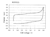
- FIG. 5 shows CV measurement results (scanning speed: 10 mV / s) in 1 M H 2 SO 4 of a symmetric 2-electrode cell using a BDND electrode (2) or an AC electrode.
- Symmetric two-electrode cell used BDND electrode (2) CV measurements saturated NaClO 4 aqueous solution (scan rate: 10 mV / s) is a graph showing the results.
- FIG. 16 is a diagram in which the electric double layer capacitance at a scanning rate of 10 to 10000 mV / s in a saturated aqueous solution of NaClO 4 in a symmetrical two-electrode cell using BDND (2) or AC electrode is calculated and plotted against the scanning rate.
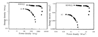
- FIG. 5 is a plot of energy density-power density in 1 M H 2 SO 4 of a symmetric two-electrode cell using BDND (2) and AC electrodes.
- FIG. 5 is a plot of energy density-power density in saturated aqueous NaClO 4 solution of a symmetric two-electrode cell using BDND (2) and AC electrodes.
- the BDND of the present invention is characterized by having a specific surface area of 110 m 2 / g or more and an electric conductivity at 20 ° C. of 5.0 ⁇ 10 ⁇ 3 S / cm or more.
- the BDND of the present invention contains boron on the surface of nanodiamond particles (ND particles).
- ND particles nanodiamond particles
- the BDND of the present invention preferably has a configuration in which a boron-containing diamond layer and / or a carbon layer is deposited on the surface of the ND particles.
- the specific surface area of BDND of the present invention is 110m 2 / g or more, preferably 150 meters 2 / g or more, more preferably 200 meters 2 / g or more, more preferably 300 meters 2 / g or more, more preferably 400 meters 2 / g or more Particularly preferably, it is 500 m 2 / g or more, and most preferably 600 m 2 / g or more.
- the upper limit of the specific surface area is, for example, 1500 m 2 / g.
- the electrical conductivity of the BDND of the present invention at 20 ° C. is 5.0 ⁇ 10 ⁇ 3 S / cm or more, preferably 10 ⁇ 10 ⁇ 3 S / cm or more, more preferably 15 ⁇ 10 ⁇ 3 S / cm or more More preferably, it is 20 ⁇ 10 ⁇ 3 S / cm or more, particularly preferably 25 ⁇ 10 ⁇ 3 S / cm or more, and most preferably 30 ⁇ 10 ⁇ 3 S / cm or more.
- the upper limit of the electrical conductivity at 20 ° C. is, for example, about 1000 S / cm.
- the boron content in the BDND of the present invention is, for example, 0.1 to 100 mg / g, preferably 0.2 to 50 mg / g, particularly preferably 0.3 to 10 mg / g, most preferably 0.4 to 5 mg / G, particularly preferably 0.5 to 2 mg / g.
- excellent conductivity can be exhibited.
- the particle diameter (D50, median diameter) of the BDND of the present invention is, for example, 200 nm or less, preferably 150 nm or less, and particularly preferably 120 nm or less.
- the lower limit of the particle diameter of BDND is, for example, 1 nm.
- BDND of the present invention in the Raman spectrum of the light source wavelength 325 nm, with a band 1370 ⁇ 1420 cm -1, and 1580 ⁇ 1620 cm -1.
- the BDND of the present invention can be produced, for example, by a CVD method (Chemical Vapor Deposition) such as a thermal CVD method, a plasma CVD method, a photo CVD method, a laser CVD method and the like.
- a CVD method Chemical Vapor Deposition
- heat, plasma, ultraviolet light, and laser light are applied to the film formation material (boron source and carbon source) in a vaporized state in the presence of a carrier gas (for example, hydrogen gas, nitrogen gas, etc.) Etc. to excite and accelerate chemical reactions to deposit boron on the surface of the ND particles as a substrate (or to deposit a boron-containing diamond layer and / or a carbon layer).
- plasma CVD in particular, microwave plasma CVD
- high quality BDND with few impurities can be obtained.
- Boron or a boron compound can be used as the boron source.
- the boron compound include boron oxide, boron carbide, boron nitride, boric acid, diborane, triethylborane, trimethoxyborane, triethoxyborane, tripropoxyborane, tri (1,1-dimethylethoxy) borane and the like. Be These can be used singly or in combination of two or more.
- Examples of the carbon source include aliphatic hydrocarbons such as methane, ethane, propane, butane, pentane, hexane, heptane and octane; alicyclic hydrocarbons such as cyclohexane; and aromatics such as benzene, toluene, xylene and ethylbenzene Hydrocarbons; Alcohols such as methanol, ethanol, isopropyl alcohol and butanol; Ketones such as acetone, methyl ethyl ketone and methyl isobutyl ketone; Ethers such as diethyl ether, dimethoxyethane, tetrahydrofuran and dioxane; Methyl acetate, ethyl acetate, isopropyl acetate and butyl acetate And the like. These can be used singly or in combination of two or more.
- a mixture of ketone and alcohol for example, a mixed solution of acetone and methanol
- the mixing ratio (v / v) of the ketone and the alcohol is, for example, 95/5 to 60/40.
- the concentration of the boron source contained in the film forming material is, for example, 10000 to 30000 ppm, preferably 15000 to 25000 ppm with respect to the carbon source.
- concentration of the boron source exceeds the above range, the crystallinity of the diamond layer and / or the carbon layer tends to be degraded.
- concentration of the boron source is below the above range, the conductivity tends to be difficult to obtain.
- the processing pressure by the CVD method is, for example, 30 to 80 Torr.
- the processing time (or film forming time) by the CVD method is, for example, 1 to 24 hours, preferably 5 to 12 hours.
- the obtained BDND is subjected to a heat treatment
- the specific surface area of the BDND can be dramatically increased, and the electric double layer capacity of the electrode including the BDND can be increased. It is preferable in point.
- the heating temperature in the heat treatment is, for example, 400 to 600 ° C., preferably 400 to 500 ° C.
- the heating time is, for example, 1 to 24 hours, preferably 5 to 12 hours.
- the particle diameter (D50, median diameter) of the ND particles as the substrate is, for example, 50 nm or less, preferably 30 nm or less, particularly preferably 20 nm or less, and most preferably 10 nm or less.
- the lower limit of the particle diameter of the ND particles as the substrate is, for example, 1 nm.
- detonation method ND that is, ND generated by detonation method
- high temperature high pressure method ND that is, ND generated by high temperature high pressure method
- detonation method ND is preferred in that it has a larger specific surface area.
- ND particle in this invention is not limited to what is obtained by the following manufacturing method.
- a molded explosive fitted with an electric detonator is installed inside a pressure-resistant container for detonation, and the container is sealed in the container in which atmospheric gas of the atmospheric composition and the used explosive coexist.
- the container is made of, for example, iron, and the volume of the container is, for example, 0.5 to 40 m 3 .
- a mixture of trinitrotoluene (TNT) and cyclotrimethylene trinitroamine or hexogen (RDX) can be used as an explosive.
- TNT trinitrotoluene
- RDX cyclotrimethylene trinitroamine or hexogen
- the mass ratio of TNT to RDX is, for example, in the range of 40/60 to 60/40.
- a detonation refers to an explosion associated with a chemical reaction in which the flame surface on which the reaction occurs travels at a high speed beyond the speed of sound.
- the used explosive partially burns incompletely and liberated carbon is used as a raw material to generate ND by the action of pressure and energy of shock wave generated by explosion.
- the formed NDs are very tightly assembled by virtue of the Coulomb interaction between crystal planes in addition to the effect of van der Waals force between adjacent primary particles or crystallites to form a cohesion body.
- the container is allowed to cool by standing at room temperature for about 24 hours, and the temperature of the container and the inside thereof is lowered.
- the ND crude product adhering to the inner wall of the container (including the adherend and wrinkles of the ND produced as described above) is scraped off with a spatula to obtain the ND crude product. to recover.
- a crude product of ND particles can be obtained.
- the oxidation treatment step is a step of removing graphite from the ND crude product using an oxidizing agent.
- the ND crude product obtained by the detonation method includes graphite (graphite), which is a carbon that partially caused incomplete combustion of the used explosive and did not form an ND crystal among liberated carbons. It originates in Graphite can be removed from the ND crude product by reacting the ND crude product with a predetermined oxidizing agent in an aqueous solvent.
- an oxygen-containing group such as a carboxyl group or a hydroxyl group can be introduced to the surface of the ND by causing the oxidizing agent to act.
- Examples of the oxidizing agent used for this oxidation treatment include chromic acid, chromic acid anhydride, dichromic acid, permanganic acid, perchloric acid, nitric acid, and mixtures thereof, and at least one acid selected therefrom. And mixed acids with other acids such as sulfuric acid and the like, and salts thereof.
- a mixed acid in particular, a mixed acid of sulfuric acid and nitric acid because it is environmentally friendly and is excellent in the effect of oxidizing and removing graphite.
- the mixing ratio of sulfuric acid and nitric acid in the mixed acid is, for example, 60/40 to 95/5 even under pressure near normal pressure (for example, 0.5 to 2 atm)
- the temperature is preferably 130 ° C. or higher (particularly preferably 150 ° C. or higher, and the upper limit is, for example, 200 ° C.), from the viewpoint of efficiently oxidizing and removing graphite.
- the lower limit is preferably 65/35, particularly preferably 70/30.
- the upper limit is preferably 90/10, particularly preferably 85/15, and most preferably 80/20.
- the proportion of nitric acid in the mixed acid exceeds the above range, the content of sulfuric acid having a high boiling point decreases, so that the reaction temperature is, for example, 120 ° C. or less under pressure near normal pressure, and the removal efficiency of graphite tends to decrease. There is. On the other hand, if the proportion of nitric acid in the mixed acid falls below the above range, nitric acid contributes greatly to the oxidation of graphite, so the removal efficiency of graphite tends to decrease.
- the amount of the oxidizing agent (in particular, the mixed acid) used is, for example, 10 to 50 parts by mass, preferably 15 to 40 parts by mass, and particularly preferably 20 to 40 parts by mass, with respect to 1 part by mass of the ND crude product.
- the amount of sulfuric acid used in the mixed acid is, for example, 5 to 48 parts by mass, preferably 10 to 35 parts by mass, particularly preferably 15 to 30 parts by mass with respect to 1 part by mass of ND crude product.
- the amount of nitric acid used in the mixed acid is, for example, 2 to 20 parts by mass, preferably 4 to 10 parts by mass, and particularly preferably 5 to 8 parts by mass, with respect to 1 part by mass of the ND crude product.
- the said mixed acid as an oxidizing agent, you may use a catalyst with mixed acid.
- a catalyst By using a catalyst, the removal efficiency of graphite can be further improved.
- copper carbonate (II) etc. can be mentioned, for example.
- the amount of the catalyst used is, for example, about 0.01 to 10 parts by mass with respect to 100 parts by mass of the ND crude product.
- the oxidation treatment temperature is, for example, 100 to 200 ° C.
- the oxidation treatment time is, for example, 1 to 24 hours.
- the oxidation treatment can be performed under reduced pressure, normal pressure, or increased pressure.
- the supernatant After such oxidation treatment, it is preferable to remove the supernatant, for example, by decantation. In the case of decantation, it is preferable to wash the solid content with water. Although the supernatant liquid at the beginning of washing is colored, it is preferable to carry out repeated washing of the solid content until the supernatant is visually clear.
- the ND particles after the oxidation treatment may be subjected to an oxidation treatment or a reduction treatment in the gas phase, if necessary.
- an oxidation treatment or a reduction treatment in the gas phase By performing the oxidation treatment in the gas phase, ND particles having many COO groups on the surface can be obtained. Also, by performing reduction treatment in the gas phase, ND particles having many C—H groups on the surface can be obtained.
- the ND particles after the oxidation treatment may be subjected to a crushing treatment, if necessary.
- a crushing treatment for example, a high shear mixer, a high shear mixer, a homomixer, a ball mill, a bead mill, a high pressure homogenizer, an ultrasonic homogenizer, a colloid mill and the like can be used.
- the crushing treatment may be carried out in a wet manner (for example, in a state of suspension in water etc.) or may be carried out in a dry manner. In the case of a dry process, it is preferable to provide a drying step before the crushing process.
- drying process In the present method, it is preferable to provide a drying step next, for example, after evaporating the liquid component from the ND-containing solution obtained through the above steps using a spray drying apparatus or an evaporator, etc.
- the solids are dried by heat drying in a drying oven.
- the heating and drying temperature is, for example, 40 to 150 ° C. Through such a drying process, ND particles are obtained.
- the electrode of the present invention includes the above-mentioned BDND as, for example, conductive particles.
- the BDND has a wide potential window and has high physical and chemical stability derived from diamond and excellent conductivity. In addition, the specific surface area is large. Therefore, the electrode including the BDND has high capacitance.
- the electrode of the present invention has a high capacitance, and the electric double layer capacity per mass of the electrode of the present invention is, for example, 3 F / g or more, preferably 5 F / g or more, particularly preferably 8 F / g or more, most preferably Is 10 F / g or more, particularly preferably 12 F / g or more.
- the upper limit of the electric double layer capacity per mass is, for example, about 20 F / g.
- the electrode of the present invention can be produced, for example, by applying an ink containing BDND to a substrate, or impregnating the substrate with the ink, and then fixing the BDND with a binder or the like.
- an insulating substrate or a conductive substrate can be used as the substrate.
- a silicon substrate, a glass substrate, a quartz substrate, a ceramic substrate, a diamond substrate etc. are mentioned, for example.
- metal substrates, such as titanium, molybdenum, niobium, aluminum, stainless steel, carbon material substrates, such as glassy carbon, etc. are mentioned, for example.
- BDND dispersion liquid in which the above-mentioned BDND is dispersed in a dispersion medium (for example, an alcohol such as ethanol etc.)
- a dispersion medium for example, an alcohol such as ethanol etc.
- the BDND concentration in the ink is, for example, preferably 20% by mass or more, and more preferably 20 to 50% by mass.
- a high shear mixer for example, a high shear mixer, a high shear mixer, a homomixer, a homomixer, a ball mill, a bead mill, a high pressure homogenizer, an ultrasonic homogenizer, a colloid mill, etc. It is preferable to disperse, and the crushing treatment is performed until the particle diameter (D50, median diameter) of BDND in the ink becomes, for example, 50 to 200 nm (preferably 50 to 150 nm, particularly preferably 50 to 120 nm). preferable.
- binder examples include polymer compounds having high proton conductivity (in particular, polymer compounds having a sulfonic acid group), and commercially available products such as, for example, trade name “Nafion” (manufactured by SIGMA-ALDRICH) Can be used.
- the amount of the binder used is, for example, about 0.1 to 5 parts by mass, preferably 0.5 to 2 parts by mass, with respect to 1 part by mass of BDND.
- the electrode of the present invention has a large electric double layer capacity, it can be suitably used, for example, as an electrode for a storage device such as an electric double layer capacitor (EDLC).
- EDLC electric double layer capacitor
- the electrode of the present invention has a wide potential window and a small background current, it is possible to analyze a trace signal that would be hidden by noise with a metal electrode. For example, environmental analysis, clinical examination, food inspection It can also be used as a sensor for micro measurement in the field of etc.
- An electricity storage device of the present invention is characterized by comprising the above-mentioned BDND electrode.
- the storage device includes an electric double layer capacitor, a hybrid capacitor (in particular, a lithium ion capacitor) and the like.
- the electric double layer capacitor preferably comprises an electrolytic solution and a separator together with the BDND electrode. Further, it is preferable that the lithium ion capacitor includes an electrode, an electrolytic solution, and a separator, use a BDND electrode as a positive electrode, and use a carbon material capable of storing lithium as a negative electrode.
- a water-based electrolyte solution and a non-water-based electrolyte solution can be used as the electrolyte solution, and a water-based electrolyte solution excellent in withstand voltage characteristics is preferable.
- aqueous electrolytes examples include aqueous solutions of acids such as hydrochloric acid, sulfuric acid, acetic acid and phosphoric acid; aqueous solutions of bases such as sodium hydroxide and ammonia; lithium perchlorate, magnesium perchlorate, calcium perchlorate, perchlorate An aqueous solution of salts such as barium acid, aluminum perchlorate, sodium perchlorate, magnesium sulfate, potassium sulfate, sodium sulfate and the like can be mentioned.
- acids such as hydrochloric acid, sulfuric acid, acetic acid and phosphoric acid
- bases such as sodium hydroxide and ammonia
- An aqueous solution of salts such as barium acid, aluminum perchlorate, sodium perchlorate, magnesium sulfate, potassium sulfate, sodium sulfate and the like can be mentioned.
- aqueous electrolytic solution it is possible to use an aqueous salt solution (in particular, an aqueous solution of perchlorate such as sodium perchlorate (for example, a saturated solution)), among others, an aqueous electric double layer having a wider potential window. It is preferable at the point from which a capacitor is obtained.
- an aqueous salt solution in particular, an aqueous solution of perchlorate such as sodium perchlorate (for example, a saturated solution)
- perchlorate for example, a saturated solution
- the aqueous electrolytic solution may contain one or more additives and / or a water-soluble organic solvent without departing from the scope of the present invention.
- the additive include salts such as tetraethylammonium perchlorate.
- the water-soluble organic solvent for example, polyhydric alcohols such as ethylene glycol, propylene glycol, butanediol, glycerin, poly C2-4 alkylene glycol (for example, diethylene glycol, triethylene glycol, tetraethylene glycol) and the like, Lactones etc. are mentioned.
- non-aqueous electrolytic solution examples include organic electrolytic solutions such as propylene carbonate, ⁇ -butyrolactone, and acetonitrile containing quaternary ammonium salts such as tetraethylammonium tetrafluoroborate and triethylmethylammonium tetrafluoroborate.
- organic electrolytic solutions such as propylene carbonate, ⁇ -butyrolactone, and acetonitrile containing quaternary ammonium salts such as tetraethylammonium tetrafluoroborate and triethylmethylammonium tetrafluoroborate.
- the lithium ion capacitor can use, as an electrolytic solution, an organic electrolytic solution in which a lithium salt such as LiBF 4 or LiPF 6 is dissolved in an organic solvent.
- separator examples include polyolefin-based separators such as PP and PE; and porous separators such as non-woven fabric and glass fiber.
- the electric double layer capacitor of the present invention can be charged and discharged by connecting a power supply between two BDND electrodes immersed in an electrolytic solution and applying a voltage. At the time of charge, electrolyte ions are adsorbed on the surface of the BDND electrode. During discharge, the cations and anions adsorbed on the BDND electrode surface are desorbed and diffused again into the electrolyte. Since the charge and discharge do not involve chemical change of the BDND electrode, the BDND electrode does not deteriorate due to heat generation accompanying a chemical reaction or the like, and a long life can be maintained.
- the storage device of the present invention includes an electrode including BDND having a large specific surface area, it can store a large charge, and can realize a large capacitance. In addition, charge and discharge can be performed at high speed compared to a general secondary battery, and the charge and discharge cycle life is excellent. Therefore, it is useful as a backup power supply for computer memory, or as an auxiliary power supply for a power storage system mounted on a railway vehicle or a hybrid vehicle.
- the sensor of the present invention is characterized by including an electrode (hereinafter sometimes referred to as "BDND electrode") including the above-mentioned BDND.
- the sensor provided with the BDND electrode according to the present invention preferably further comprises, for example, voltage control means for controlling the potential of the BDND electrode, and current measurement means for measuring a change in current flowing through the electrode.
- a voltage lead wire and a current lead wire are connected to the BDND electrode, and the potential is controlled by the voltage control means.
- a voltage control means As a voltage control means, a potentiostat, a constant potential power supply device etc. are mentioned, for example.
- Examples of the current measurement means include an ammeter, a galvanometer, and the like.
- the BDND electrode is brought into contact with the electrolyte solution containing the detection target sample together with the counter electrode, and the current value is measured while controlling the potential by the voltage control means.
- a voltage is applied, an oxidation or reduction reaction occurs due to the electrolysis of the sample to be detected on the BDND electrode, but the current value associated with this reaction has a correlation with the concentration of the sample, so the current measured by the current measurement means
- the concentration of the sample to be detected can be calculated from the value.
- counter electrode for example, platinum, carbon, stainless steel, gold, diamond, SnO 2 or the like can be used.
- the sensor of the present invention is provided with a BDND electrode having a wide potential window and a small background current, it is possible to analyze a trace signal that would be hidden by noise with a metal electrode, for example, environmental analysis, clinical examination It can also be used for trace measurement in the field of food inspection and the like.
- ND (1) powder, median diameter (particle diameter D50) measured by dynamic light scattering method: 5 nm
- the BDND (1) was subjected to heat treatment at 425 ° C. for 8 hours in an air atmosphere to obtain BDND (2).
- the particle diameter (median diameter: D50) of the obtained BDND (1), (2) and BDDP (1) to (3) was measured by a dynamic light scattering method.
- FIG. 1 shows the particle diameter measurement results of BDND (1) and (2).
- the BET specific surface area was measured by a nitrogen adsorption method.
- a glass capillary with an inner diameter of 1 mm was filled with BDND (1), and the electrical conductivity was calculated from the direct current resistance at both ends.
- BDND (1) and (2) were excellent in conductivity, and furthermore, the specific surface area was larger than BDDP.
- BDND (2) a diffraction pattern of a diamond crystal was observed in X-ray diffraction, and it was confirmed that diamond was contained.
- a graphitic laminate structure was observed in addition to the diamond lattice plane (FIG. 4).
- the BDND of the present invention is a composite having a structure in which an sp 2 carbon layer containing boron is deposited on the surface of nanodiamond particles.
- Example 2 (Production of Electrode) 10 mg of the obtained BDND (1) was dispersed in 0.5 mL of 30% by mass ethanol to prepare a BDND ink. After casting 20 ⁇ L of BDND ink on a glassy carbon electrode, which is a current collector, and drying it, 5% by mass Nafion (a hydrophobic side chain having a sulfonic acid group is bonded to a hydrophobic Teflon (registered trademark) skeleton) The BDND electrode (1) was obtained by casting and coating 10 ⁇ L of the perfluorocarbon (having the composition) on the outermost surface.
- Example 3 (Production of Electrode) A BDND electrode (2) was obtained in the same manner as in Example 2 except that BDND (2) was used instead of BDND (1).
- BDND (2) capable of applying a large cell voltage in an aqueous solution is an electrode material suitable for realizing a high energy density aqueous EDLC.
- a saturated NaClO 4 aqueous solution capable of applying a large cell voltage in an aqueous solution is an electrolyte suitable for realizing a high energy density aqueous EDLC.
- the electrostatic energy that can be stored in the EDLC is expressed by CV 2/2 (C: electric double layer capacity, V: the cell voltage).
- the electric double layer capacity at each scanning speed was calculated and plotted against the scanning speed (FIG. 9). Comparing the capacity per mass of the electrode active material (BDND (1), (2) or AC), although the capacity is large at the AC electrode at low speed scanning of 100 mV / s or less, BDND at high speed scanning of 100 mV / s or more It was found that the electrodes (1) and (2) became larger. This is an electrode material in which AC has micropores developed inside the particle, and a large electric double layer capacity is obtained using its large specific surface area, but the electrolyte ions in the micropores are difficult to move. Although the adsorption and desorption with respect to the surface can not follow the potential change during high-speed scanning, the capacity decreases, but such large capacity reduction did not occur because BDND (1) and (2) do not have micropores It is considered to be a thing.
- BDNDs (1) and (2) are considered to be electrode materials suitable for producing high-output EDLCs, because their capacity is unlikely to decrease even at high-speed scanning.
- the energy density was calculated using the result of the electric double layer capacity when changing the scanning speed.
- the cell voltage (V) was calculated at 2.8 V for both the BDND electrode (2) and the AC electrode. Similar to the graph of the electric double layer capacity, it was found that the BDND electrode (2) exhibits a larger energy density than the AC electrode at a high scanning speed (20 mV / s or more).
- the BDND electrodes (1) and (2) exhibit a larger capacity than the AC electrode in the range of 10 to 1000 mV / s. This is because AC has micropores and therefore has a low bulk density, while BDND (1) and (2) have no micropores and have a bulk density greater than AC. it is conceivable that. Therefore, BDND (1) and (2) are considered to be useful for the production of space-saving EDLC devices.
- FIG. 11 shows a Lagon plot (energy density-power density plot) of a symmetric 2-electrode cell using a BDND electrode (2) or an AC electrode. From these results, it can be seen that the BDND electrode (2) can produce a water-based EDLC device having a higher energy density and a higher output density than the AC electrode. In particular, regarding the characteristics per volume, the power density can be increased while maintaining a high energy density, which is considered to be useful for the production of a compact high-power device.
- BDND electrode (2) in saturated NaClO 4 aqueous solution is compared with BDND electrode (2) in 1 MH 2 SO 4 Then, it was confirmed that the energy density was improved while maintaining the power density by the increase of the cell voltage. Therefore, it can be confirmed that the BDND electrode (2) in the saturated NaClO 4 aqueous solution is improved in performance as compared with the BDND electrode (2) in 1 MH 2 SO 4 .
- a boron-doped nanodiamond characterized by having a specific surface area of 110 m 2 / g or more and an electric conductivity at 20 ° C. of 5.0 ⁇ 10 ⁇ 3 S / cm or more.
- the boron-doped nanodiamond according to [1] having a median diameter of 200 nm or less.
- [6] An electrode comprising the boron-doped nanodiamond according to any one of [1] to [4].
- the electrode according to [6] having an electric double layer capacity per mass of 3 F / g or more.
- a sensor comprising the electrode according to [6] or [7].
- a storage device comprising the electrode according to [6] or [7].
- the storage device according to [9] which is an electric double layer capacitor.
- the electricity storage device according to [9] which is a water-based electric double layer capacitor using a saturated aqueous solution of perchlorate as an electrolytic solution.
- the storage device according to [9] which is a lithium ion capacitor.
- a power supply comprising the power storage device according to any one of [9] to [12].
- the BDND of the present invention has high physical stability, chemical stability, excellent conductivity and large specific surface area derived from diamond. Therefore, when the BDND of the present invention is used, an electrode having a large capacitance can be obtained.
- the electrode including the BDND of the present invention is highly sensitive, has a large electric double layer capacity per mass, and has a wide potential window. Therefore, it is useful as an electrode for electrochemical sensors and storage devices.
Landscapes
- Engineering & Computer Science (AREA)
- Chemical & Material Sciences (AREA)
- Power Engineering (AREA)
- Organic Chemistry (AREA)
- Microelectronics & Electronic Packaging (AREA)
- Materials Engineering (AREA)
- General Life Sciences & Earth Sciences (AREA)
- Life Sciences & Earth Sciences (AREA)
- Geology (AREA)
- Inorganic Chemistry (AREA)
- Manufacturing & Machinery (AREA)
- Nanotechnology (AREA)
- Crystallography & Structural Chemistry (AREA)
- Carbon And Carbon Compounds (AREA)
- Electric Double-Layer Capacitors Or The Like (AREA)
Abstract
Provided are a boron-doped nanodiamond having a large specific surface area and a high electrical conductivity, an electrode comprising the boron-doped nanodiamond, and a sensor or an electrical storage device that includes the electrode. The boron-doped nanodiamond is characterized by having a specific surface area of 110 m2/g or more and an electrical conductivity at 20°C of 5.0×10⁻³ S/cm or more. The boron-doped nanodiamond preferably has a median diameter of 200 nm or less. Additionally, the electrode is characterized by comprising the boron-doped nanodiamond.
Description
本発明は、キャパシタ用電極材料等として有用な、ホウ素ドープナノダイヤモンド、ホウ素ドープナノダイヤモンドを含む電極、及び前記電極を備えたセンサー若しくは蓄電デバイスに関する。尚、本発明のホウ素ドープナノダイヤモンドの用途は、キャパシタ用電極材料に限定されるものではない。本願は、2017年11月16日に日本に出願した、特願2017−220842号の優先権を主張し、その内容をここに援用する。
The present invention relates to a boron-doped nanodiamond, an electrode containing boron-doped nanodiamond, and a sensor or a storage device provided with the electrode, which is useful as an electrode material or the like for a capacitor. The application of the boron-doped nanodiamond of the present invention is not limited to the electrode material for capacitors. Priority is claimed on Japanese Patent Application No. 2017-220842, filed on Nov. 16, 2017, the content of which is incorporated herein by reference.
絶縁性のダイヤモンドにホウ素を高濃度にドープするとホールが生成し(p型半導体)、金属的導電性が付与されることが知られている。そして、ダイヤモンドにホウ素を高濃度にドープしたホウ素ドープダイヤモンド(BDD:Boron Doped Diamond)は、ダイヤモンド由来の高い物理的安定性及び化学的安定性、並びに優れた導電性を有し、当該ホウ素ドープダイヤモンドを含む電極は広い電位窓(水の電気分解が起きない電位範囲)と小さいバックグラウンド電流を有するため、貴金属や炭素などの電極材料に比べ、電気化学分析や電気分解に有効な機能性電極材料として注目されている。
It is known that when insulating diamond is highly doped with boron, holes are generated (p-type semiconductor) and metallic conductivity is imparted. And, boron-doped diamond (BDD: Boron Doped Diamond) in which diamond is heavily doped with boron has high physical stability and chemical stability derived from diamond, and excellent conductivity, Since the electrode containing a large potential window (potential range where electrolysis of water does not occur) and a small background current, functional electrode materials that are effective for electrochemical analysis and electrolysis compared to electrode materials such as noble metals and carbon Has been noted as.
ホウ素ドープダイヤモンドの製造方法として、例えば特許文献1には、ホウ素とダイヤモンド粒子とアルカリ土類炭酸塩粉末との混合物において、5.0~8.0GPaの加圧条件下、1300~1800℃の温度で加熱することにより、ホウ素をダイヤモンド粒子にドープし、ホウ素ドープダイヤモンド粒子を製造する方法が開示されている。しかし、上記特許文献1のホウ素ドープダイヤモンド粒子の平均粒径は1~8μmであり、比表面積が小さく、蓄電デバイス用の電極として使用するのに十分な静電容量の確保が困難であった。
As a method for producing boron-doped diamond, for example, in Patent Document 1, a mixture of boron, diamond particles and alkaline earth carbonate powder is heated at a temperature of 1300 to 1800 ° C. under a pressure of 5.0 to 8.0 GPa. Discloses a method of doping boron into diamond particles by heating at a temperature of about 40.degree. C. to produce boron-doped diamond particles. However, the average particle diameter of the boron-doped diamond particles described in Patent Document 1 is 1 to 8 μm, the specific surface area is small, and it is difficult to secure sufficient capacitance for use as an electrode for a storage device.
また、特許文献2には、ホウ素とナノダイヤモンド粒子を水素雰囲気下において700~1000℃で加熱すると、比表面積が大きいホウ素ドープナノダイヤモンドが得られることが記載されている。しかし、この方法で得られたホウ素ドープナノダイヤモンドは、導電性の点で未だ不十分であった。
Further, Patent Document 2 describes that when boron and nanodiamond particles are heated at 700 to 1000 ° C. in a hydrogen atmosphere, boron-doped nanodiamonds having a large specific surface area can be obtained. However, the boron-doped nanodiamond obtained by this method is still insufficient in terms of conductivity.
従って、本発明の目的は、比表面積が大きく、高い電気伝導度を有するホウ素ドープナノダイヤモンド(以後、「BDND」と称する場合がある)を提供することにある。
本発明の他の目的は、前記BDNDを含む電極を提供することにある。
本発明の他の目的は、前記電極を備えたセンサーを提供することにある。
本発明の他の目的は、前記電極を備えた蓄電デバイスを提供することにある。 Accordingly, an object of the present invention is to provide a boron-doped nanodiamond (hereinafter sometimes referred to as “BDND”) having a large specific surface area and high electrical conductivity.
Another object of the present invention is to provide an electrode comprising the BDND.
Another object of the present invention is to provide a sensor comprising the electrode.
Another object of the present invention is to provide a storage device provided with the electrode.
本発明者等は上記課題を解決するため鋭意検討した結果、ナノダイヤモンド粒子の表面に、化学気相成長法(CVD法:Chemical Vapor Deposition)によりホウ素を含有するダイヤモンド層及び/又は炭素層を形成することによって得られるBDNDは比表面積が大きく、高い電気伝導度を有すること、当該BDNDを電極に用いれば静電容量が大きい電極が得られることを見いだした。本発明はこれらの知見に基づいて完成させたものである。
As a result of intensive studies to solve the above problems, the present inventors formed a boron-containing diamond layer and / or a carbon layer on the surface of nanodiamond particles by the chemical vapor deposition method (CVD method: Chemical Vapor Deposition). It has been found that the BDND obtained by conducting this method has a large specific surface area and high electrical conductivity, and that an electrode having a large capacitance can be obtained by using the BDND as an electrode. The present invention has been completed based on these findings.
すなわち、本発明は、比表面積が110m2/g以上であり、且つ20℃における電気伝導度が5.0×10−3S/cm以上であることを特徴とする、ホウ素ドープナノダイヤモンドを提供する。
That is, the present invention provides a boron-doped nanodiamond characterized in that the specific surface area is 110 m 2 / g or more and the electrical conductivity at 20 ° C. is 5.0 × 10 −3 S / cm or more. Do.
本発明は、また、メディアン径が200nm以下である前記のホウ素ドープナノダイヤモンドを提供する。
The present invention also provides the boron-doped nanodiamond described above, which has a median diameter of 200 nm or less.
本発明は、また、光源波長325nmのラマンスペクトルにおいて、1370~1420cm−1、及び1580~1620cm−1にバンドを有する前記のホウ素ドープナノダイヤモンドを提供する。
The present invention is also in the Raman spectrum of the light source wavelength 325 nm, to provide the boron-doped nanodiamond having 1370 ~ 1420 cm -1, and band 1580 ~ 1620 cm -1.
本発明は、また、前記のホウ素ドープナノダイヤモンドを含む電極を提供する。
The present invention also provides an electrode comprising the boron-doped nanodiamond described above.
本発明は、また、質量当たりの電気二重層容量が3F/g以上である前記の電極を提供する。
The present invention also provides the above-mentioned electrode having an electric double layer capacity per mass of 3 F / g or more.
本発明は、また、前記の電極を備えたセンサーを提供する。
The present invention also provides a sensor comprising the above electrode.
本発明は、また、前記の電極を備えた蓄電デバイスを提供する。
The present invention also provides a storage device provided with the above electrode.
本発明のBDNDは、ダイヤモンド由来の高い物理的安定性、化学的安定性、優れた導電性、及び大きな比表面積を有する。そのため、本発明のBDNDを使用すれば、静電容量が大きい電極が得られる。
また、本発明のBDNDを含む電極は高感度であり、且つ質量当たりの電気二重層容量が大きい。すなわち、静電容量が大きい。また、広い電位窓を有する。そのため、前記電極は、電気化学センサーや蓄電デバイス用電極として有用である。 The BDND of the present invention has high physical stability, chemical stability, excellent conductivity and large specific surface area derived from diamond. Therefore, when the BDND of the present invention is used, an electrode having a large capacitance can be obtained.
In addition, the electrode containing the BDND of the present invention is highly sensitive and has a large electric double layer capacity per mass. That is, the capacitance is large. In addition, it has a wide potential window. Therefore, the electrode is useful as an electrode for an electrochemical sensor or a storage device.
[BDND]
本発明のBDNDは、比表面積が110m2/g以上であり、且つ20℃における電気伝導度が5.0×10−3S/cm以上であることを特徴とする。 [BDND]
The BDND of the present invention is characterized by having a specific surface area of 110 m 2 / g or more and an electric conductivity at 20 ° C. of 5.0 × 10 −3 S / cm or more.
本発明のBDNDは、比表面積が110m2/g以上であり、且つ20℃における電気伝導度が5.0×10−3S/cm以上であることを特徴とする。 [BDND]
The BDND of the present invention is characterized by having a specific surface area of 110 m 2 / g or more and an electric conductivity at 20 ° C. of 5.0 × 10 −3 S / cm or more.
本発明のBDNDは、ナノダイヤモンド粒子(ND粒子)の表面にホウ素を含有する。本発明のBDNDは、好ましくは、ND粒子の表面に、ホウ素を含有するダイヤモンド層及び/又は炭素層が堆積した構成を有する。
The BDND of the present invention contains boron on the surface of nanodiamond particles (ND particles). The BDND of the present invention preferably has a configuration in which a boron-containing diamond layer and / or a carbon layer is deposited on the surface of the ND particles.
本発明のBDNDの比表面積は110m2/g以上であり、好ましくは150m2/g以上、より好ましくは200m2/g以上、更に好ましくは300m2/g以上、更に好ましくは400m2/g以上、特に好ましくは500m2/g以上、最も好ましくは600m2/g以上である。尚、比表面積の上限は、例えば1500m2/gである。
The specific surface area of BDND of the present invention is 110m 2 / g or more, preferably 150 meters 2 / g or more, more preferably 200 meters 2 / g or more, more preferably 300 meters 2 / g or more, more preferably 400 meters 2 / g or more Particularly preferably, it is 500 m 2 / g or more, and most preferably 600 m 2 / g or more. The upper limit of the specific surface area is, for example, 1500 m 2 / g.
本発明のBDNDの20℃における電気伝導度は5.0×10⁻³S/cm以上であり、好ましくは10×10−3S/cm以上、より好ましくは15×10−3S/cm以上、更に好ましくは20×10−3S/cm以上、特に好ましくは25×10−3S/cm以上、最も好ましくは30×10−3S/cm以上である。尚、20℃における電気伝導度の上限は、例えば1000S/cm程度である。
The electrical conductivity of the BDND of the present invention at 20 ° C. is 5.0 × 10 −3 S / cm or more, preferably 10 × 10 −3 S / cm or more, more preferably 15 × 10 −3 S / cm or more More preferably, it is 20 × 10 −3 S / cm or more, particularly preferably 25 × 10 −3 S / cm or more, and most preferably 30 × 10 −3 S / cm or more. The upper limit of the electrical conductivity at 20 ° C. is, for example, about 1000 S / cm.
本発明のBDNDにおけるホウ素含有量は、例えば0.1~100mg/gであり、好ましくは0.2~50mg/g、特に好ましくは0.3~10mg/g、最も好ましくは0.4~5mg/g、とりわけ好ましくは0.5~2mg/gである。本発明のBDNDが前記範囲でホウ素を含有すると、優れた導電性を発揮することができる。
The boron content in the BDND of the present invention is, for example, 0.1 to 100 mg / g, preferably 0.2 to 50 mg / g, particularly preferably 0.3 to 10 mg / g, most preferably 0.4 to 5 mg / G, particularly preferably 0.5 to 2 mg / g. When the BDND of the present invention contains boron in the above-mentioned range, excellent conductivity can be exhibited.
本発明のBDNDの粒子径(D50、メディアン径)は例えば200nm以下であり、好ましくは150nm以下、特に好ましくは120nm以下である。BDNDの粒子径の下限は、例えば1nmである。粒子径が上記範囲を上回ると比表面積が低下し、当該BDNDを含む電極の静電容量が低下する傾向がある。BDNDの粒子径は、動的光散乱法によって測定することができる。
The particle diameter (D50, median diameter) of the BDND of the present invention is, for example, 200 nm or less, preferably 150 nm or less, and particularly preferably 120 nm or less. The lower limit of the particle diameter of BDND is, for example, 1 nm. When the particle size exceeds the above range, the specific surface area is reduced, and the capacitance of the electrode including the BDND tends to be reduced. The particle size of BDND can be measured by dynamic light scattering.
また、本発明のBDNDは、光源波長325nmのラマンスペクトルにおいて、1370~1420cm−1、及び1580~1620cm−1にバンドを有する。
Further, BDND of the present invention, in the Raman spectrum of the light source wavelength 325 nm, with a band 1370 ~ 1420 cm -1, and 1580 ~ 1620 cm -1.
本発明のBDNDは、例えば、熱CVD法、プラズマCVD法、光CVD法、レーザーCVD法等のCVD法(Chemical Vapor Deposition:化学気相成長法)によって製造することができる。詳細には、必要に応じてキャリアガス(例えば、水素ガス、窒素ガス等)の存在下で、気化した状態の成膜材料(ホウ素源と炭素源)に、熱、プラズマ、紫外光、レーザー光などのエネルギーを付与して化学反応を励起・促進して、基材としてのND粒子の表面にホウ素を付着させる(若しくは、ホウ素を含有するダイヤモンド層及び/又は炭素層を積層する)ことによって製造することができる。本発明においては、なかでも、プラズマCVD法(特に、マイクロ波プラズマCVD法)を採用することが、不純物が少なく高品質なBDNDが得られる点で好ましい。
The BDND of the present invention can be produced, for example, by a CVD method (Chemical Vapor Deposition) such as a thermal CVD method, a plasma CVD method, a photo CVD method, a laser CVD method and the like. In detail, if necessary, heat, plasma, ultraviolet light, and laser light are applied to the film formation material (boron source and carbon source) in a vaporized state in the presence of a carrier gas (for example, hydrogen gas, nitrogen gas, etc.) Etc. to excite and accelerate chemical reactions to deposit boron on the surface of the ND particles as a substrate (or to deposit a boron-containing diamond layer and / or a carbon layer). can do. In the present invention, it is preferable to use plasma CVD (in particular, microwave plasma CVD), in particular, in that high quality BDND with few impurities can be obtained.
前記ホウ素源としては、ホウ素又はホウ素化合物を使用することができる。前記ホウ素化合物としては、例えば、酸化ホウ素、炭化ホウ素、窒化ホウ素、ホウ酸、ジボラン、トリエチルボラン、トリメトキシボラン、トリエトキシボラン、トリプロポキシボラン、トリ(1,1−ジメチルエトキシ)ボラン等が挙げられる。これらは1種を単独で、又は2種以上を組み合わせて使用することができる。
Boron or a boron compound can be used as the boron source. Examples of the boron compound include boron oxide, boron carbide, boron nitride, boric acid, diborane, triethylborane, trimethoxyborane, triethoxyborane, tripropoxyborane, tri (1,1-dimethylethoxy) borane and the like. Be These can be used singly or in combination of two or more.
前記炭素源としては、例えば、メタン、エタン、プロパン、ブタン、ペンタン、ヘキサン、ヘプタン、オクタン等の脂肪族炭化水素;シクロヘキサン等の脂環式炭化水素;ベンゼン、トルエン、キシレン、エチルベンゼン等の芳香族炭化水素;メタノール、エタノール、イソプロピルアルコール、ブタノール等のアルコール;アセトン、メチルエチルケトン、メチルイソブチルケトン等のケトン;ジエチルエーテル、ジメトキシエタン、テトラヒドロフラン、ジオキサン等のエーテル;酢酸メチル、酢酸エチル、酢酸イソプロピル、酢酸ブチル等のエステル等が挙げられる。これらは1種を単独で、又は2種以上を組み合わせて使用することができる。
Examples of the carbon source include aliphatic hydrocarbons such as methane, ethane, propane, butane, pentane, hexane, heptane and octane; alicyclic hydrocarbons such as cyclohexane; and aromatics such as benzene, toluene, xylene and ethylbenzene Hydrocarbons; Alcohols such as methanol, ethanol, isopropyl alcohol and butanol; Ketones such as acetone, methyl ethyl ketone and methyl isobutyl ketone; Ethers such as diethyl ether, dimethoxyethane, tetrahydrofuran and dioxane; Methyl acetate, ethyl acetate, isopropyl acetate and butyl acetate And the like. These can be used singly or in combination of two or more.
前記炭素源としては、ケトンとアルコールの混合物(例えば、アセトンとメタノール混合溶液)を使用することが、気化し易く、且つ上記ホウ素源の溶解性に優れる点で好ましい。ケトンとアルコールの混合比(v/v)は、例えば95/5~60/40である。
It is preferable to use a mixture of ketone and alcohol (for example, a mixed solution of acetone and methanol) as the carbon source in view of easy vaporization and excellent solubility of the boron source. The mixing ratio (v / v) of the ketone and the alcohol is, for example, 95/5 to 60/40.
また、成膜材料に含まれるホウ素源の濃度としては、炭素源に対して、例えば10000~30000ppm、好ましくは15000~25000ppmである。ホウ素源の濃度が上記範囲を上回ると、ダイヤモンド層及び/又は炭素層の結晶性が劣化する傾向がある。一方、ホウ素源の濃度が上記範囲を下回ると、導電性が得られにくくなる傾向がある。
Further, the concentration of the boron source contained in the film forming material is, for example, 10000 to 30000 ppm, preferably 15000 to 25000 ppm with respect to the carbon source. When the concentration of the boron source exceeds the above range, the crystallinity of the diamond layer and / or the carbon layer tends to be degraded. On the other hand, when the concentration of the boron source is below the above range, the conductivity tends to be difficult to obtain.
CVD法による処理時圧力は、例えば30~80Torrである。
The processing pressure by the CVD method is, for example, 30 to 80 Torr.
CVD法による処理時間(若しくは、成膜時間)は、例えば1~24時間、好ましくは5~12時間である。
The processing time (or film forming time) by the CVD method is, for example, 1 to 24 hours, preferably 5 to 12 hours.
CVD法によってND粒子の表面にホウ素をドープした(詳細には、ND粒子の表面にホウ素を含有するダイヤモンド層及び/又は炭素層を成長させた)後は、得られたBDNDに加熱処理を施して当該BDNDに含まれるダイヤモンド層及び/又は炭素層の構造を最適化することで、BDNDの比表面積を飛躍的に高めることができ、当該BDNDを含む電極の電気二重層容量を高めることができる点で好ましい。
After doping the surface of the ND particles with boron by the CVD method (specifically, growing a diamond layer and / or a carbon layer containing boron on the surface of the ND particles), the obtained BDND is subjected to a heat treatment By optimizing the structure of the diamond layer and / or carbon layer contained in the BDND, the specific surface area of the BDND can be dramatically increased, and the electric double layer capacity of the electrode including the BDND can be increased. It is preferable in point.
前記加熱処理における加熱温度は、例えば400~600℃、好ましくは400~500℃である。また、加熱時間は、例えば1~24時間、好ましくは5~12時間である。
The heating temperature in the heat treatment is, for example, 400 to 600 ° C., preferably 400 to 500 ° C. The heating time is, for example, 1 to 24 hours, preferably 5 to 12 hours.
基材としてのND粒子の粒子径(D50、メディアン径)は、例えば50nm以下であり、好ましくは30nm以下、特に好ましくは20nm以下、最も好ましくは10nm以下である。基材としてのND粒子の粒子径の下限は、例えば1nmである。
The particle diameter (D50, median diameter) of the ND particles as the substrate is, for example, 50 nm or less, preferably 30 nm or less, particularly preferably 20 nm or less, and most preferably 10 nm or less. The lower limit of the particle diameter of the ND particles as the substrate is, for example, 1 nm.
基材としてのND粒子としては、例えば、爆轟法ND(すなわち、爆轟法によって生成したND)や、高温高圧法ND(すなわち、高温高圧法によって生成したND)を使用することができる。本発明においては、なかでも、より比表面積が大きい点で爆轟法NDが好ましい。
As ND particles as a substrate, for example, detonation method ND (that is, ND generated by detonation method) or high temperature high pressure method ND (that is, ND generated by high temperature high pressure method) can be used. In the present invention, among these, detonation method ND is preferred in that it has a larger specific surface area.
以下に、ND粒子の製造方法の一例を以下に説明するが、本発明におけるND粒子は以下の製造方法によって得られるものに限定されない。
Although an example of the manufacturing method of ND particle is demonstrated below, ND particle in this invention is not limited to what is obtained by the following manufacturing method.
(生成工程)
成形された爆薬に電気雷管が装着されたものを爆轟用の耐圧性容器の内部に設置し、容器内において大気組成の常圧の気体と使用爆薬とが共存する状態で、容器を密閉する。容器は例えば鉄製で、容器の容積は例えば0.5~40m3である。爆薬としては、トリニトロトルエン(TNT)とシクロトリメチレントリニトロアミンすなわちヘキソーゲン(RDX)との混合物を使用することができる。TNTとRDXの質量比(TNT/RDX)は、例えば40/60~60/40の範囲である。 (Generation process)
A molded explosive fitted with an electric detonator is installed inside a pressure-resistant container for detonation, and the container is sealed in the container in which atmospheric gas of the atmospheric composition and the used explosive coexist. . The container is made of, for example, iron, and the volume of the container is, for example, 0.5 to 40 m 3 . As an explosive, a mixture of trinitrotoluene (TNT) and cyclotrimethylene trinitroamine or hexogen (RDX) can be used. The mass ratio of TNT to RDX (TNT / RDX) is, for example, in the range of 40/60 to 60/40.
生成工程では、次に、電気雷管を起爆させ、容器内で爆薬を爆轟させる。爆轟とは、化学反応に伴う爆発のうち反応の生じる火炎面が音速を超えた高速で移動するものをいう。爆轟の際、使用爆薬が部分的に不完全燃焼を起こして遊離した炭素を原料として、爆発で生じた衝撃波の圧力とエネルギーの作用によってNDが生成する。生成したNDは、隣接する一次粒子ないし結晶子の間がファンデルワールス力の作用に加えて結晶面間クーロン相互作用が寄与して非常に強固に集成し、凝着体を成す。
In the production process, next, the electric detonator is detonated and the explosive is detonated in the container. A detonation refers to an explosion associated with a chemical reaction in which the flame surface on which the reaction occurs travels at a high speed beyond the speed of sound. At the time of detonation, the used explosive partially burns incompletely and liberated carbon is used as a raw material to generate ND by the action of pressure and energy of shock wave generated by explosion. The formed NDs are very tightly assembled by virtue of the Coulomb interaction between crystal planes in addition to the effect of van der Waals force between adjacent primary particles or crystallites to form a cohesion body.
生成工程では、次に、室温において24時間程度放置することにより放冷し、容器およびその内部を降温させる。この放冷の後、容器の内壁に付着しているND粗生成物(上述のようにして生成したNDの凝着体および煤を含む)をヘラで掻き取る作業を行い、ND粗生成物を回収する。以上のような方法によって、ND粒子の粗生成物を得ることができる。
Next, in the production process, the container is allowed to cool by standing at room temperature for about 24 hours, and the temperature of the container and the inside thereof is lowered. After this cooling, the ND crude product adhering to the inner wall of the container (including the adherend and wrinkles of the ND produced as described above) is scraped off with a spatula to obtain the ND crude product. to recover. By the above method, a crude product of ND particles can be obtained.
(酸化処理工程)
酸化処理工程は、酸化剤を用いてND粗生成物からグラファイトを除去する工程である。爆轟法で得られるND粗生成物にはグラファイト(黒鉛)が含まれるが、このグラファイトは、使用爆薬が部分的に不完全燃焼を起こして遊離した炭素のうちND結晶を形成しなかった炭素に由来する。ND粗生成物に、水溶媒中で所定の酸化剤を作用させることにより、ND粗生成物からグラファイトを除去することができる。また、酸化剤を作用させることにより、ND表面にカルボキシル基や水酸基などの酸素含有基を導入することができる。 (Oxidation treatment process)
The oxidation treatment step is a step of removing graphite from the ND crude product using an oxidizing agent. The ND crude product obtained by the detonation method includes graphite (graphite), which is a carbon that partially caused incomplete combustion of the used explosive and did not form an ND crystal among liberated carbons. It originates in Graphite can be removed from the ND crude product by reacting the ND crude product with a predetermined oxidizing agent in an aqueous solvent. In addition, an oxygen-containing group such as a carboxyl group or a hydroxyl group can be introduced to the surface of the ND by causing the oxidizing agent to act.
この酸化処理に用いられる酸化剤としては、例えば、クロム酸、無水クロム酸、二クロム酸、過マンガン酸、過塩素酸、硝酸、及びこれらの混合物や、これらから選択される少なくとも1種の酸と他の酸(例えば、硫酸等)との混酸、及びこれらの塩が挙げられる。本発明においては、なかでも、混酸(特に、硫酸と硝酸との混酸)を使用することが、環境に優しく、且つグラファイトを酸化・除去する作用に優れる点で好ましい。
Examples of the oxidizing agent used for this oxidation treatment include chromic acid, chromic acid anhydride, dichromic acid, permanganic acid, perchloric acid, nitric acid, and mixtures thereof, and at least one acid selected therefrom. And mixed acids with other acids such as sulfuric acid and the like, and salts thereof. In the present invention, it is preferable to use a mixed acid (in particular, a mixed acid of sulfuric acid and nitric acid) because it is environmentally friendly and is excellent in the effect of oxidizing and removing graphite.
前記混酸における硫酸と硝酸との混合割合(前者/後者;質量比)は、例えば60/40~95/5であることが、常圧付近の圧力(例えば、0.5~2atm)の下でも、例えば130℃以上(特に好ましくは150℃以上。尚、上限は、例えば200℃)の温度で、効率よくグラファイトを酸化して除去することができる点で好ましい。下限は、好ましくは65/35、特に好ましくは70/30である。また、上限は、好ましくは90/10、特に好ましくは85/15、最も好ましくは80/20である。
The mixing ratio of sulfuric acid and nitric acid in the mixed acid (former / latter; mass ratio) is, for example, 60/40 to 95/5 even under pressure near normal pressure (for example, 0.5 to 2 atm) For example, the temperature is preferably 130 ° C. or higher (particularly preferably 150 ° C. or higher, and the upper limit is, for example, 200 ° C.), from the viewpoint of efficiently oxidizing and removing graphite. The lower limit is preferably 65/35, particularly preferably 70/30. The upper limit is preferably 90/10, particularly preferably 85/15, and most preferably 80/20.
混酸における硝酸の割合が上記範囲を上回ると、高沸点を有する硫酸の含有量が少なくなるため、常圧付近の圧力下では、反応温度が例えば120℃以下となり、グラファイトの除去効率が低下する傾向がある。一方、混酸における硝酸の割合が上記範囲を下回ると、グラファイトの酸化に大きく貢献するのは硝酸であるため、グラファイトの除去効率が低下する傾向がある。
When the proportion of nitric acid in the mixed acid exceeds the above range, the content of sulfuric acid having a high boiling point decreases, so that the reaction temperature is, for example, 120 ° C. or less under pressure near normal pressure, and the removal efficiency of graphite tends to decrease. There is. On the other hand, if the proportion of nitric acid in the mixed acid falls below the above range, nitric acid contributes greatly to the oxidation of graphite, so the removal efficiency of graphite tends to decrease.
酸化剤(特に、前記混酸)の使用量は、ND粗生成物1質量部に対して、例えば10~50質量部、好ましくは15~40質量部、特に好ましくは20~40質量部である。また、前記混酸中の硫酸の使用量は、ND粗生成物1質量部に対して、例えば5~48質量部、好ましくは10~35質量部、特に好ましくは15~30質量部であり、前記混酸中の硝酸の使用量は、ND粗生成物1質量部に対して、例えば2~20質量部、好ましくは4~10質量部、特に好ましくは5~8質量部である。
The amount of the oxidizing agent (in particular, the mixed acid) used is, for example, 10 to 50 parts by mass, preferably 15 to 40 parts by mass, and particularly preferably 20 to 40 parts by mass, with respect to 1 part by mass of the ND crude product. The amount of sulfuric acid used in the mixed acid is, for example, 5 to 48 parts by mass, preferably 10 to 35 parts by mass, particularly preferably 15 to 30 parts by mass with respect to 1 part by mass of ND crude product The amount of nitric acid used in the mixed acid is, for example, 2 to 20 parts by mass, preferably 4 to 10 parts by mass, and particularly preferably 5 to 8 parts by mass, with respect to 1 part by mass of the ND crude product.
また、酸化剤として前記混酸を使用する場合、混酸と共に触媒を使用しても良い。触媒を使用することにより、グラファイトの除去効率を一層向上することができる。前記触媒としては、例えば、炭酸銅(II)等を挙げることができる。触媒の使用量は、ND粗生成物100質量部に対して例えば0.01~10質量部程度である。
Moreover, when using the said mixed acid as an oxidizing agent, you may use a catalyst with mixed acid. By using a catalyst, the removal efficiency of graphite can be further improved. As said catalyst, copper carbonate (II) etc. can be mentioned, for example. The amount of the catalyst used is, for example, about 0.01 to 10 parts by mass with respect to 100 parts by mass of the ND crude product.
酸化処理温度は例えば100~200℃である。酸化処理時間は例えば1~24時間である。酸化処理は、減圧下、常圧下、または加圧下で行うことが可能である。
The oxidation treatment temperature is, for example, 100 to 200 ° C. The oxidation treatment time is, for example, 1 to 24 hours. The oxidation treatment can be performed under reduced pressure, normal pressure, or increased pressure.
このような酸化処理の後、例えばデカンテーションにより上澄みを除去することが好ましい。また、デカンテーションの際には、固形分の水洗を行うことが好ましい。水洗当初の上澄み液は着色しているが、上澄み液が目視で透明になるまで、当該固形分の水洗を反復して行うことが好ましい。
After such oxidation treatment, it is preferable to remove the supernatant, for example, by decantation. In the case of decantation, it is preferable to wash the solid content with water. Although the supernatant liquid at the beginning of washing is colored, it is preferable to carry out repeated washing of the solid content until the supernatant is visually clear.
また、酸化処理後のND粒子には、必要に応じて、気相にて酸化処理や還元処理を施しても良い。気相にて酸化処理を施すことにより、表面にC=O基を多く有するND粒子が得られる。また、気相にて還元処理を施すことにより、表面にC−H基を多く有するND粒子が得られる。
In addition, the ND particles after the oxidation treatment may be subjected to an oxidation treatment or a reduction treatment in the gas phase, if necessary. By performing the oxidation treatment in the gas phase, ND particles having many COO groups on the surface can be obtained. Also, by performing reduction treatment in the gas phase, ND particles having many C—H groups on the surface can be obtained.
更に酸化処理後のND粒子には、必要に応じて、解砕処理を施してもよい。解砕処理には、例えば、高剪断ミキサー、ハイシアーミキサー、ホモミキサー、ボールミル、ビーズミル、高圧ホモジナイザー、超音波ホモジナイザー、コロイドミル等を使用することができる。尚、解砕処理は湿式(例えば、水等に懸濁した状態での解砕処理)で行ってもよいし、乾式で行ってもよい。乾式で行う場合は、解砕処理前に乾燥工程を設けることが好ましい。
Furthermore, the ND particles after the oxidation treatment may be subjected to a crushing treatment, if necessary. For the crushing treatment, for example, a high shear mixer, a high shear mixer, a homomixer, a ball mill, a bead mill, a high pressure homogenizer, an ultrasonic homogenizer, a colloid mill and the like can be used. The crushing treatment may be carried out in a wet manner (for example, in a state of suspension in water etc.) or may be carried out in a dry manner. In the case of a dry process, it is preferable to provide a drying step before the crushing process.
(乾燥工程)
本方法では、次に、乾燥工程を設けることが好ましく、例えば、上記工程を経て得られたND含有溶液から噴霧乾燥装置やエバポレーター等を使用して液分を蒸発させた後、これによって生じる残留固形分を乾燥用オーブン内での加熱乾燥によって乾燥させる。加熱乾燥温度は、例えば40~150℃である。このような乾燥工程を経ることにより、ND粒子が得られる。 (Drying process)
In the present method, it is preferable to provide a drying step next, for example, after evaporating the liquid component from the ND-containing solution obtained through the above steps using a spray drying apparatus or an evaporator, etc. The solids are dried by heat drying in a drying oven. The heating and drying temperature is, for example, 40 to 150 ° C. Through such a drying process, ND particles are obtained.
[電極]
本発明の電極は、例えば導電性粒子として、上記BDNDを含む。上記BDNDは広い電位窓を有し、ダイヤモンド由来の高い物理的安定性及び化学的安定性、並びに優れた導電性を有する。また、比表面積が大きい。そのため、当該BDNDを含む電極は高い静電容量を有する。 [electrode]
The electrode of the present invention includes the above-mentioned BDND as, for example, conductive particles. The BDND has a wide potential window and has high physical and chemical stability derived from diamond and excellent conductivity. In addition, the specific surface area is large. Therefore, the electrode including the BDND has high capacitance.
本発明の電極は高い静電容量を有し、本発明の電極の質量当たりの電気二重層容量は、例えば3F/g以上、好ましくは5F/g以上、特に好ましくは8F/g以上、最も好ましくは10F/g以上、とりわけ好ましくは12F/g以上である。尚、質量当たりの電気二重層容量の上限は、例えば20F/g程度である。
The electrode of the present invention has a high capacitance, and the electric double layer capacity per mass of the electrode of the present invention is, for example, 3 F / g or more, preferably 5 F / g or more, particularly preferably 8 F / g or more, most preferably Is 10 F / g or more, particularly preferably 12 F / g or more. The upper limit of the electric double layer capacity per mass is, for example, about 20 F / g.
本発明の電極は、例えば、BDNDを含むインクを基材に塗布、若しくは基材に含浸させ、その後、BDNDをバインダー等で固定することにより製造することができる。
The electrode of the present invention can be produced, for example, by applying an ink containing BDND to a substrate, or impregnating the substrate with the ink, and then fixing the BDND with a binder or the like.
前記基材としては、絶縁性基板や導電性基板を使用することができる。絶縁性基板としては、例えば、シリコン基板、ガラス基板、石英基板、セラミックス基板、ダイヤモンド基板等が挙げられる。また、導電性基板としては、例えば、チタン、モリブデン、ニオブ、アルミニウム、ステンレス等の金属基板や、ガラス状炭素等の炭素材料基板等が挙げられる。
As the substrate, an insulating substrate or a conductive substrate can be used. As an insulating substrate, a silicon substrate, a glass substrate, a quartz substrate, a ceramic substrate, a diamond substrate etc. are mentioned, for example. Moreover, as a conductive substrate, metal substrates, such as titanium, molybdenum, niobium, aluminum, stainless steel, carbon material substrates, such as glassy carbon, etc. are mentioned, for example.
BDNDを含むインクとしては、例えば、上述のBDNDを分散媒(例えば、エタノール等のアルコール等)中に分散させたBDND分散液を使用することができる。前記インク中のBDND濃度としては、例えば20質量%以上が好ましく、より好ましくは20~50質量%である。
As the ink containing BDND, for example, a BDND dispersion liquid in which the above-mentioned BDND is dispersed in a dispersion medium (for example, an alcohol such as ethanol etc.) can be used. The BDND concentration in the ink is, for example, preferably 20% by mass or more, and more preferably 20 to 50% by mass.
BDNDを分散媒中に分散させる際には、例えば、高剪断ミキサー、ハイシアーミキサー、ホモミキサー、ボールミル、ビーズミル、高圧ホモジナイザー、超音波ホモジナイザー、コロイドミル等を使用してBDNDを分散媒中に高分散させることが好ましく、インク中のBDNDの粒子径(D50、メディアン径)が、例えば50~200nm(好ましくは50~150nm、特に好ましくは50~120nm)となるまで、解砕処理を施すことが好ましい。
When dispersing BDND in a dispersion medium, for example, a high shear mixer, a high shear mixer, a homomixer, a homomixer, a ball mill, a bead mill, a high pressure homogenizer, an ultrasonic homogenizer, a colloid mill, etc. It is preferable to disperse, and the crushing treatment is performed until the particle diameter (D50, median diameter) of BDND in the ink becomes, for example, 50 to 200 nm (preferably 50 to 150 nm, particularly preferably 50 to 120 nm). preferable.
BDNDを含むインクを基材に塗布若しくは含浸させた後は、乾燥処理を施して分散媒を蒸発させることが好ましい。
After applying or impregnating the ink containing BDND to the substrate, it is preferable to carry out a drying process to evaporate the dispersion medium.
前記バインダーとしては、例えば、高いプロトン導電性を有する高分子化合物(特に、スルホン酸基を有する高分子化合物)が挙げられ、例えば、商品名「ナフィオン」(SIGMA−ALDRICH社製)等の市販品を使用することができる。
Examples of the binder include polymer compounds having high proton conductivity (in particular, polymer compounds having a sulfonic acid group), and commercially available products such as, for example, trade name “Nafion” (manufactured by SIGMA-ALDRICH) Can be used.
前記バインダーの使用量としては、BDND1質量部に対して例えば0.1~5質量部程度、好ましくは0.5~2質量部である。
The amount of the binder used is, for example, about 0.1 to 5 parts by mass, preferably 0.5 to 2 parts by mass, with respect to 1 part by mass of BDND.
本発明の電極は電気二重層容量が大きいため、例えば、電気二重層キャパシタ(EDLC)等の蓄電デバイス用の電極として好適に使用することができる。また、本発明の電極は広い電位窓と小さいバックグラウンド電流を有するため、金属電極ではノイズに隠れてしまうような微量な信号も分析することができるので、例えば、環境分析、臨床検査、食品検査等の分野における微量測定用センサーに使用することもできる。
Since the electrode of the present invention has a large electric double layer capacity, it can be suitably used, for example, as an electrode for a storage device such as an electric double layer capacitor (EDLC). In addition, since the electrode of the present invention has a wide potential window and a small background current, it is possible to analyze a trace signal that would be hidden by noise with a metal electrode. For example, environmental analysis, clinical examination, food inspection It can also be used as a sensor for micro measurement in the field of etc.
[蓄電デバイス]
本発明の蓄電デバイスは、上記BDND電極を備えることを特徴とする。蓄電デバイスには、電気二重層キャパシタやハイブリッドキャパシタ(特に、リチウムイオンキャパシタ)等が含まれる。 [Electric storage device]
An electricity storage device of the present invention is characterized by comprising the above-mentioned BDND electrode. The storage device includes an electric double layer capacitor, a hybrid capacitor (in particular, a lithium ion capacitor) and the like.
電気二重層キャパシタは、上記BDND電極と共に電解液とセパレーターとを備えることが好ましい。また、リチウムイオンキャパシタは、電極と電解液とセパレーターとを備え、正極としてBDND電極を使用し、負極としてリチウムを吸蔵可能な炭素材料を使用することが好ましい。
The electric double layer capacitor preferably comprises an electrolytic solution and a separator together with the BDND electrode. Further, it is preferable that the lithium ion capacitor includes an electrode, an electrolytic solution, and a separator, use a BDND electrode as a positive electrode, and use a carbon material capable of storing lithium as a negative electrode.
本発明の電気二重層キャパシタは、電解液として水系電解液と非水系電解液を使用することができ、耐電圧特性の優れた水系電解液が好ましい。水系電解液としては、例えば、塩酸、硫酸、酢酸、リン酸等の酸の水溶液;水酸化ナトリウム、アンモニア等の塩基の水溶液;過塩素酸リチウム、過塩素酸マグネシウム、過塩素酸カルシウム、過塩素酸バリウム、過塩素酸アルミニウム、過塩素酸ナトリウム、硫酸マグネシウム、硫酸カリウム、硫酸ナトリウム等の塩の水溶液等が挙げられる。水系電解液としては、なかでも、塩の水溶液(特に、過塩素酸ナトリウム等の過塩素酸塩の(例えば、飽和)水溶液)を使用することが、より一層広い電位窓を有する水系電気二重層キャパシタが得られる点で好ましい。
In the electric double layer capacitor of the present invention, a water-based electrolyte solution and a non-water-based electrolyte solution can be used as the electrolyte solution, and a water-based electrolyte solution excellent in withstand voltage characteristics is preferable. Examples of aqueous electrolytes include aqueous solutions of acids such as hydrochloric acid, sulfuric acid, acetic acid and phosphoric acid; aqueous solutions of bases such as sodium hydroxide and ammonia; lithium perchlorate, magnesium perchlorate, calcium perchlorate, perchlorate An aqueous solution of salts such as barium acid, aluminum perchlorate, sodium perchlorate, magnesium sulfate, potassium sulfate, sodium sulfate and the like can be mentioned. As the aqueous electrolytic solution, it is possible to use an aqueous salt solution (in particular, an aqueous solution of perchlorate such as sodium perchlorate (for example, a saturated solution)), among others, an aqueous electric double layer having a wider potential window. It is preferable at the point from which a capacitor is obtained.
また、水系電解液は、本発明の趣旨を逸脱しない範囲で添加剤や水溶性有機溶媒を、それぞれ1種又は2種以上含んでいてもよい。前記添加剤としては、例えば、過塩素酸テトラエチルアンモニウム等の塩が挙げられる。また、前記水溶性有機溶媒としては、例えば、エチレングリコール、プロピレングリコール、ブタンジオール、グリセリン、ポリC2−4アルキレングリコール(例えば、ジエチレングリコール、トリエチレングリコール、テトラエチレングリコール)等の多価アルコールや、ラクトン類等が挙げられる。
In addition, the aqueous electrolytic solution may contain one or more additives and / or a water-soluble organic solvent without departing from the scope of the present invention. Examples of the additive include salts such as tetraethylammonium perchlorate. Further, as the water-soluble organic solvent, for example, polyhydric alcohols such as ethylene glycol, propylene glycol, butanediol, glycerin, poly C2-4 alkylene glycol (for example, diethylene glycol, triethylene glycol, tetraethylene glycol) and the like, Lactones etc. are mentioned.
前記非水系電解液としては、例えば、テトラエチルアンモニウムテトラフルオロボレート、トリエチルメチルアンモニウムテトラフルオロボレートなどの4級アンモニウム塩を含む、プロピレンカーボネート、γ−ブチロラクトン、アセトニトリル等の有機系電解液が挙げられる。
Examples of the non-aqueous electrolytic solution include organic electrolytic solutions such as propylene carbonate, γ-butyrolactone, and acetonitrile containing quaternary ammonium salts such as tetraethylammonium tetrafluoroborate and triethylmethylammonium tetrafluoroborate.
リチウムイオンキャパシタは、電解液として、LiBF4、LiPF6等のリチウム塩を有機溶媒に溶解した有機系電解液を使用することができる。
The lithium ion capacitor can use, as an electrolytic solution, an organic electrolytic solution in which a lithium salt such as LiBF 4 or LiPF 6 is dissolved in an organic solvent.
前記セパレーターとしては、例えば、PP、PEなどのポリオレフィン系セパレーター;不織布、ガラス繊維などの多孔質セパレーター等が挙げられる。
Examples of the separator include polyolefin-based separators such as PP and PE; and porous separators such as non-woven fabric and glass fiber.
本発明の電気二重層キャパシタは、電解液に浸漬した二枚のBDND電極間に電源を繋いで電圧を印加することで充放電できる。充電時は電解質イオンがBDND電極表面に吸着する。放電時にはBDND電極表面に吸着していた陽イオン並びに陰イオンが脱離して、電解液中に再び拡散する。充放電には、BDND電極の化学的変化を伴わないため、BDND電極が化学反応に伴う発熱等により劣化することがなく、長寿命を保つことができる。
The electric double layer capacitor of the present invention can be charged and discharged by connecting a power supply between two BDND electrodes immersed in an electrolytic solution and applying a voltage. At the time of charge, electrolyte ions are adsorbed on the surface of the BDND electrode. During discharge, the cations and anions adsorbed on the BDND electrode surface are desorbed and diffused again into the electrolyte. Since the charge and discharge do not involve chemical change of the BDND electrode, the BDND electrode does not deteriorate due to heat generation accompanying a chemical reaction or the like, and a long life can be maintained.
本発明の蓄電デバイスは、比表面積が大きいBDNDを含む電極を備えるため、大きな電荷を蓄えることができ、大きい静電容量を実現し得る。また、一般的な二次電池に比べて高速での充放電が可能であり、充放電サイクル寿命に優れる。そのため、コンピュータのメモリのバックアップ用電源や、鉄道車両に搭載した電力貯蔵システムやハイブリッド車の補助電源として有用である。
Since the storage device of the present invention includes an electrode including BDND having a large specific surface area, it can store a large charge, and can realize a large capacitance. In addition, charge and discharge can be performed at high speed compared to a general secondary battery, and the charge and discharge cycle life is excellent. Therefore, it is useful as a backup power supply for computer memory, or as an auxiliary power supply for a power storage system mounted on a railway vehicle or a hybrid vehicle.
[センサー]
本発明のセンサーは、上記BDNDを含む電極(以後、「BDND電極」と称する場合がある)を備えることを特徴とする。本発明の、BDND電極を備えたセンサーは更に、例えば、BDND電極の電位を制御する電圧制御手段と、前記電極に流れる電流値の変化を計測する電流計測手段とを備えることが好ましい。 [sensor]
The sensor of the present invention is characterized by including an electrode (hereinafter sometimes referred to as "BDND electrode") including the above-mentioned BDND. The sensor provided with the BDND electrode according to the present invention preferably further comprises, for example, voltage control means for controlling the potential of the BDND electrode, and current measurement means for measuring a change in current flowing through the electrode.
また、BDND電極には電圧リード線・電流リード線が接続され、電圧制御手段によって電位が制御されることが好ましい。
Further, it is preferable that a voltage lead wire and a current lead wire are connected to the BDND electrode, and the potential is controlled by the voltage control means.
電圧制御手段としては、例えば、ポテンショスタット、定電位電源装置等が挙げられる。
As a voltage control means, a potentiostat, a constant potential power supply device etc. are mentioned, for example.
電流計測手段としては、例えば、電流計、検流器等が挙げられる。
Examples of the current measurement means include an ammeter, a galvanometer, and the like.
対電極と共に、BDND電極を検出対象試料を含む電解質溶液に接触させ、電圧制御手段により電位を制御しながら電流値を計測する。電圧を印加すると、BDND電極上で検出対象試料の電気分解による酸化又は還元反応が生じるが、この反応に伴う電流値は、試料の濃度と相関関係を有するため、電流計測手段により計測された電流値から検出対象試料の濃度を算出することができる。
The BDND electrode is brought into contact with the electrolyte solution containing the detection target sample together with the counter electrode, and the current value is measured while controlling the potential by the voltage control means. When a voltage is applied, an oxidation or reduction reaction occurs due to the electrolysis of the sample to be detected on the BDND electrode, but the current value associated with this reaction has a correlation with the concentration of the sample, so the current measured by the current measurement means The concentration of the sample to be detected can be calculated from the value.
前記対電極としては、例えば、白金、炭素、ステンレス、金、ダイヤモンド、SnO2等を使用することができる。
As the counter electrode, for example, platinum, carbon, stainless steel, gold, diamond, SnO 2 or the like can be used.
本発明のセンサーは、広い電位窓と小さいバックグラウンド電流を有するBDND電極を備えるため、金属電極ではノイズに隠れてしまうような微量な信号も分析することができるので、例えば、環境分析、臨床検査、食品検査等の分野における微量測定に使用することもできる。
Since the sensor of the present invention is provided with a BDND electrode having a wide potential window and a small background current, it is possible to analyze a trace signal that would be hidden by noise with a metal electrode, for example, environmental analysis, clinical examination It can also be used for trace measurement in the field of food inspection and the like.
以下、実施例により本発明をより具体的に説明するが、本発明はこれらの実施例により限定されるものではない。
EXAMPLES Hereinafter, the present invention will be more specifically described by way of examples, but the present invention is not limited by these examples.
実施例1(BDNDの製造)
(生成工程)
まず、成形された爆薬に電気雷管が装着されたものを爆轟用の耐圧性容器(鉄製容器、容積:15m3)の内部に設置して容器を密閉した。爆薬としては、TNTとRDXとの混合物(TNT/RDX(質量比)=50/50)0.50kgを使用した。次に、電気雷管を起爆させ、容器内で爆薬を爆轟させた。次に、室温で24時間静置して、容器およびその内部を降温させた。この放冷の後、容器の内壁に付着しているND粗生成物(ND粒子の凝着体と煤を含む)をヘラで掻き取る作業を行い、ND粗生成物を回収した。ND粗生成物の回収量は0.025kgであった。 Example 1 (Production of BDND)
(Generation process)
First, a shaped explosive provided with an electric detonator was placed inside a pressure-resistant container for detonation (iron container, volume: 15 m 3 ) to seal the container. As an explosive, 0.50 kg of a mixture of TNT and RDX (TNT / RDX (mass ratio) = 50/50) was used. Next, the electric detonator was detonated and the explosive was detonated in the container. Next, the container and the inside thereof were cooled by standing at room temperature for 24 hours. After this free cooling, an operation of scraping off the ND crude product (including an aggregate of ND particles and wrinkles) adhering to the inner wall of the container was performed with a spatula to recover the ND crude product. The amount of recovered ND crude product was 0.025 kg.
(酸化処理工程)
次に、50℃の冷媒を循環させた凝縮器と前記凝縮器に接続されたアルカリトラップとを備えた反応器中において、1atm下、反応器を加熱しつつ、生成工程で得られたND粗生成物(3g)と濃硫酸(80.6g)と炭酸銅(触媒量)とを反応器に仕込んだ。
そこへ、発煙硝酸(20.4g、前記濃硫酸と硝酸の割合が80/20(前者/後者;質量比)となる量)を滴下した。反応の進行に伴って蒸発した硝酸、及び生成したH2Oは凝縮器で凝縮して反応器内に戻した。一方、NO、NO2、CO、及びCO2は凝縮器に接続されたアルカリトラップで捕集した。このとき、反応温度は150℃であった。
反応開始から48時間経過後、反応器の加熱を停止し、反応器内を室温まで冷却した。冷却後、デカンテーションにより、固形分(ND凝着体を含む)の水洗を行った。水洗当初の上澄み液は着色しているところ、上澄み液が目視で透明になるまで、デカンテーションによる当該固形分の水洗を反復して行った。 (Oxidation treatment process)
Next, in a reactor equipped with a condenser in which a refrigerant of 50 ° C. is circulated and an alkali trap connected to the condenser, the ND crude obtained in the production step is heated while heating the reactor under 1 atm. The product (3 g), concentrated sulfuric acid (80.6 g) and copper carbonate (catalytic amount) were charged to the reactor.
Therein, fuming nitric acid (20.4 g, an amount such that the ratio of the concentrated sulfuric acid to the nitric acid becomes 80/20 (the former / the latter; mass ratio)) was dropped. As the reaction progressed, nitric acid evaporated and H 2 O formed were condensed by the condenser and returned to the reactor. On the other hand, NO, NO 2 , CO and CO 2 were collected by an alkali trap connected to a condenser. At this time, the reaction temperature was 150.degree.
After 48 hours from the start of the reaction, heating of the reactor was stopped and the reactor was cooled to room temperature. After cooling, the solid content (including ND aggregates) was washed with water by decantation. The supernatant liquid at the beginning of washing with water was colored, and the washing of the solid content by decantation was repeated until the supernatant was visually clear.
(解砕工程)
次に、ビーズミル(商品名「ウルトラアペックスミルUAM−015」、寿工業(株)製)を使用して、前工程を経て得られたスラリー300mLを解砕処理に付した。本処理では、解砕メディアとしてジルコニアビーズ(直径0.03mm)を使用し、ミル容器内に充填されるビーズの量はミル容器の容積に対して60%とし.ミル容器内で回転するローターピンの周速は10m/sとした。また、装置を循環させるスラリーの流速を10L/hとして90分間の解砕処理を行った。 (Crushing process)
Next, 300 mL of the slurry obtained through the previous step was subjected to crushing using a bead mill (trade name "Ultra Apex Mill UAM-015" manufactured by Kotobuki Kogyo Co., Ltd.). In this treatment, zirconia beads (diameter 0.03 mm) were used as the crushing media, and the amount of beads packed in the mill vessel was 60% of the volume of the mill vessel. The circumferential speed of the rotor pin rotating in the mill container was 10 m / s. In addition, the crushing process was performed for 90 minutes by setting the flow rate of the slurry circulating through the apparatus to 10 L / h.
(遠心分離工程)
次に、上述の解砕工程を経たNDを含有する溶液から、遠心力の作用を利用した分級操作によって粗大粒子を除去した(遠心分離処理)。本工程の遠心分離処理において、遠心力は20000×gとし、遠心時間は10分とした。これにより、黒色透明のND水分散液(1)を得た。 (Centrifugation process)
Next, coarse particles were removed from the ND-containing solution subjected to the above-mentioned crushing step by classification operation using the action of centrifugal force (centrifugation treatment). In the centrifugation in this step, the centrifugal force was 20000 × g, and the centrifugation time was 10 minutes. Thus, a black transparent ND aqueous dispersion (1) was obtained.
(乾燥工程)
次に、遠心分離工程で得られたND水分散液(1)からエバポレーターを使用して液分を蒸発させた後、残留固形分を乾燥用オーブンを使用して120℃で加熱して乾燥させた。 (Drying process)
Next, after evaporating the liquid portion from the ND aqueous dispersion (1) obtained in the centrifugation step using an evaporator, the remaining solid content is dried by heating at 120 ° C. using a drying oven The
以上のようにして、ND(1)(粉体、動的光散乱法によって測定したメディアン径(粒径D50):5nm)を得た。
As described above, ND (1) (powder, median diameter (particle diameter D50) measured by dynamic light scattering method: 5 nm) was obtained.
(ホウ素ドープ工程)
得られたND(1)を基材として、MPCVD法により、下記条件下でホウ素をドープした。原料溶液として、炭素源としてのアセトン/メタノール混合溶液(9:1,v/v)に、トリメトキシボランを、炭素原子に対するホウ素原子濃度が20000ppmとなる割合で添加したものを使用したこれにより、BDND(1)を得た。
<MPCVD条件>
マイクロ波出力:1300W
圧力:50Torr
水素ガス流量:400sccm
成長時間:8h (Boron doping process)
Boron was doped under the following conditions by the MPCVD method using the obtained ND (1) as a substrate. As a raw material solution, one obtained by adding trimethoxyborane to an acetone / methanol mixed solution (9: 1, v / v) as a carbon source at a ratio of 20000 ppm of boron atom to carbon atoms is used. Obtained BDND (1).
<MPCVD conditions>
Microwave output: 1300W
Pressure: 50 Torr
Hydrogen gas flow rate: 400 sccm
Growth time: 8 h
(加熱処理工程)
BDND(1)を、空気雰囲気下、425℃で8時間の加熱処理に付して、BDND(2)を得た。 (Heating process)
The BDND (1) was subjected to heat treatment at 425 ° C. for 8 hours in an air atmosphere to obtain BDND (2).
BDND(1)を、空気雰囲気下、425℃で8時間の加熱処理に付して、BDND(2)を得た。 (Heating process)
The BDND (1) was subjected to heat treatment at 425 ° C. for 8 hours in an air atmosphere to obtain BDND (2).
比較例1~3
基材をND(1)から、ダイヤモンド粒子(DP(1)~(3))に変更した以外は実施例1のBDND(1)と同様にしてホウ素ドープダイヤモンド粒子(BDDP(1)~(3))を得た。 Comparative Examples 1 to 3
Boron-doped diamond particles (BDDP (1) to (3) were produced in the same manner as BDND (1) in Example 1 except that the substrate was changed from ND (1) to diamond particles (DP (1) to (3)). )) Got.
(粒子径、比表面積、及び電気伝導度の測定)
得られたBDND(1)、(2)、及びBDDP(1)~(3)について、粒子径(メディアン径:D50)を動的光散乱法によって測定した。図1にBDND(1)、(2)の粒子径測定結果を示す。
また、BET比表面積を窒素吸着法により測定した。
また、20℃において、内径1mmのガラスキャピラリーにBDND(1)を充填し、両端の直流抵抗から電気伝導度を算出した。 (Measurement of particle size, specific surface area, and electrical conductivity)
The particle diameter (median diameter: D50) of the obtained BDND (1), (2) and BDDP (1) to (3) was measured by a dynamic light scattering method. FIG. 1 shows the particle diameter measurement results of BDND (1) and (2).
Further, the BET specific surface area was measured by a nitrogen adsorption method.
At 20 ° C., a glass capillary with an inner diameter of 1 mm was filled with BDND (1), and the electrical conductivity was calculated from the direct current resistance at both ends.
結果を下記表にまとめて示す。

The results are summarized in the following table.
表1より、BDND(1)、(2)は導電性に優れ、その上、BDDPに比べ比表面積が大きいことが確かめられた。
また、ND(1)、BDND(1)、(2)のUVラマンスペクトル(光源波長:325nm)測定結果より、BDND(1)、(2)では、sp2炭素由来のDバンドおよびGバンドが顕著に観察された(図2、3)。
更に、BDND(2)は、X線回折ではダイヤモンド結晶の回折パターンが観測され、ダイヤモンドが含まれていることが確かめられた。
更にまた、BDND(2)のTEM観察の結果、ダイヤモンド格子面のほかにグラファイト状積層構造が観察された(図4)。
また、BDND(2)の元素分析をICP−AES法により行った結果、620mg/kgのホウ素が含まれていることがわかった。
以上の結果より、本発明のBDNDはナノダイヤモンド粒子の表面にホウ素を含むsp2炭素層が堆積された構造を有する複合体であることが示唆された。 From Table 1, it was confirmed that BDND (1) and (2) were excellent in conductivity, and furthermore, the specific surface area was larger than BDDP.
In addition, from the measurement results of UV Raman spectra (light source wavelength: 325 nm) of ND (1), BDND (1), (2), in BDND (1), (2), D band and G band derived from sp 2 carbon are It was remarkably observed (Figures 2 and 3).
Furthermore, in BDND (2), a diffraction pattern of a diamond crystal was observed in X-ray diffraction, and it was confirmed that diamond was contained.
Furthermore, as a result of TEM observation of BDND (2), a graphitic laminate structure was observed in addition to the diamond lattice plane (FIG. 4).
Moreover, as a result of conducting an elemental analysis of BDND (2) by the ICP-AES method, it turned out that 620 mg / kg of boron is contained.
From the above results, it has been suggested that the BDND of the present invention is a composite having a structure in which an sp 2 carbon layer containing boron is deposited on the surface of nanodiamond particles.
実施例2(電極の製造)
得られたBDND(1)10mgを0.5mLの30質量%エタノールに分散させて、BDNDインクを調製した。
集電体であるガラス状炭素電極上にBDNDインク20μLをキャストし、乾燥させた後、5質量%ナフィオン(疎水性テフロン(登録商標)骨格に、スルホン酸基を持つパーフルオロ側鎖が結合した構成を有するパーフルオロカーボン)10μLを最表面にキャストし、被覆することでBDND電極(1)を得た。 Example 2 (Production of Electrode)
10 mg of the obtained BDND (1) was dispersed in 0.5 mL of 30% by mass ethanol to prepare a BDND ink.
After casting 20 μL of BDND ink on a glassy carbon electrode, which is a current collector, and drying it, 5% by mass Nafion (a hydrophobic side chain having a sulfonic acid group is bonded to a hydrophobic Teflon (registered trademark) skeleton) The BDND electrode (1) was obtained by casting andcoating 10 μL of the perfluorocarbon (having the composition) on the outermost surface.
得られたBDND(1)10mgを0.5mLの30質量%エタノールに分散させて、BDNDインクを調製した。
集電体であるガラス状炭素電極上にBDNDインク20μLをキャストし、乾燥させた後、5質量%ナフィオン(疎水性テフロン(登録商標)骨格に、スルホン酸基を持つパーフルオロ側鎖が結合した構成を有するパーフルオロカーボン)10μLを最表面にキャストし、被覆することでBDND電極(1)を得た。 Example 2 (Production of Electrode)
10 mg of the obtained BDND (1) was dispersed in 0.5 mL of 30% by mass ethanol to prepare a BDND ink.
After casting 20 μL of BDND ink on a glassy carbon electrode, which is a current collector, and drying it, 5% by mass Nafion (a hydrophobic side chain having a sulfonic acid group is bonded to a hydrophobic Teflon (registered trademark) skeleton) The BDND electrode (1) was obtained by casting and
実施例3(電極の製造)
BDND(1)に代えてBDND(2)を使用した以外は実施例2と同様にしてBDND電極(2)を得た。 Example 3 (Production of Electrode)
A BDND electrode (2) was obtained in the same manner as in Example 2 except that BDND (2) was used instead of BDND (1).
BDND(1)に代えてBDND(2)を使用した以外は実施例2と同様にしてBDND電極(2)を得た。 Example 3 (Production of Electrode)
A BDND electrode (2) was obtained in the same manner as in Example 2 except that BDND (2) was used instead of BDND (1).
比較例4(電極の製造)
BDND(1)に代えてBDDP(1)を使用した以外は実施例2と同様にしてBDDP電極(1)を得た。 Comparative Example 4 (Production of Electrode)
A BDDP electrode (1) was obtained in the same manner as in Example 2 except that BDDP (1) was used instead of BDND (1).
BDND(1)に代えてBDDP(1)を使用した以外は実施例2と同様にしてBDDP電極(1)を得た。 Comparative Example 4 (Production of Electrode)
A BDDP electrode (1) was obtained in the same manner as in Example 2 except that BDDP (1) was used instead of BDND (1).
比較例5(電極の製造)
BDND(1)に代えてBDDP(2)を使用した以外は実施例2と同様にしてBDDP電極(2)を得た。 Comparative Example 5 (Production of Electrode)
A BDDP electrode (2) was obtained in the same manner as in Example 2 except that BDDP (2) was used instead of BDND (1).
BDND(1)に代えてBDDP(2)を使用した以外は実施例2と同様にしてBDDP電極(2)を得た。 Comparative Example 5 (Production of Electrode)
A BDDP electrode (2) was obtained in the same manner as in Example 2 except that BDDP (2) was used instead of BDND (1).
比較例6(電極の製造)
BDND(1)に代えてBDDP(3)を使用した以外は実施例2と同様の方法でBDDP電極(3)を得た。 Comparative Example 6 (Production of Electrode)
A BDDP electrode (3) was obtained in the same manner as in Example 2 except that BDDP (3) was used instead of BDND (1).
BDND(1)に代えてBDDP(3)を使用した以外は実施例2と同様の方法でBDDP電極(3)を得た。 Comparative Example 6 (Production of Electrode)
A BDDP electrode (3) was obtained in the same manner as in Example 2 except that BDDP (3) was used instead of BDND (1).
比較例7(電極の製造)
BDND(1)に代えて活性炭(AC;比表面積1318m2/g)を使用した以外は実施例2と同様の方法でAC電極を得た。この場合、ACは導電性が低いため、導電助剤としてアセチレンブラック(AB)をAC:AB(質量比)が8:1となるように添加した。 Comparative Example 7 (Production of Electrode)
An AC electrode was obtained in the same manner as in Example 2 except that activated carbon (AC; specific surface area 1318 m 2 / g) was used instead of BDND (1). In this case, since AC has low conductivity, acetylene black (AB) is added as a conductive aid so that AC: AB (mass ratio) becomes 8: 1.
[評価]
実施例及び比較例で得られた電極の性能を評価した。
[1]電位窓、セル電圧測定
(1−1)BDND電極(2)およびAC電極の、1MのH2SO4中のCV(走査速度:10mV/s)を測定した。対極に白金線、参照極にAg/AgCl電極を用いた3電極系にて実施した。
電位窓はAC電極では1.5V程度であったのに対し、BDND電極(2)では1.9Vであり、広いことがわかった(図5)。
(1−2)超純水100mL中に過剰量の過塩素酸ナトリウム(NaClO4)を加えた後、吸引ろ過を行い、過剰分の過塩素酸ナトリウムを除去することで、飽和NaClO4水溶液を得た。BDND電極(2)の、飽和NaClO4水溶液中でのCV(走査速度:10mV/s)を測定した。対極に白金線、参照極にAg/AgCl電極を用いた3電極系にて実施した。
電位窓は3.1Vであり、として過塩素酸塩水溶液を使用することにより電位窓が広くなることがわかった(図6)。 [Evaluation]
The performances of the electrodes obtained in Examples and Comparative Examples were evaluated.
[1] Potential window, cell voltage measurement (1-1) CV (scanning speed: 10 mV / s) in 1 M H 2 SO 4 of BDND electrode (2) and AC electrode was measured. It implemented by the 3-electrode system which used the platinum wire for the counter electrode, and the Ag / AgCl electrode for the reference electrode.
The potential window was about 1.5 V for the AC electrode, while it was 1.9 V for the BDND electrode (2), which was found to be wide (FIG. 5).
(1-2) Add an excess amount of sodium perchlorate (NaClO 4 ) into 100 mL of ultrapure water, and then perform suction filtration to remove excess sodium perchlorate to obtain a saturated NaClO 4 aqueous solution. Obtained. The CV (scanning speed: 10 mV / s) of the BDND electrode (2) in a saturated aqueous solution of NaClO 4 was measured. It implemented by the 3-electrode system which used the platinum wire for the counter electrode, and the Ag / AgCl electrode for the reference electrode.
The potential window was 3.1 V, and it was found that the potential window became wider by using a perchlorate aqueous solution (FIG. 6).
(1−3)BDND電極(2)、又はAC電極を使用した対称2電極セルで、1MのH2SO4中のCV測定(cyclic voltammetry、走査速度:10mV/s)を行ったところ、AC電極ではセル電圧(両極間の電位差)を0.8V以上とすると溶媒(水)の電解が起き始めたのに対し、BDND電極(2)では、1.8Vまで電圧印加可能であることがわかった(図7)。BDDP電極(3)についても同様にCV測定を行ったところ、セル電圧(両極間の電位差)を1.6V以上とすると溶媒(水)の電解が起き始めた。
(1−4)BDND電極(2)を使用した対称2電極セルで、飽和NaClO4水溶液中のCV測定(走査速度:10mV/s)を行ったところ、BDND電極(2)は2.8Vまで電圧印加可能であることがわかった(図8)。また、2.8V以上に印加すると溶媒(水)の電解が起き始めた。 (1-3) CV measurement (cyclic voltammetry, scanning rate: 10 mV / s) in 1 M H 2 SO 4 was performed in a symmetrical 2-electrode cell using a BDND electrode (2) or an AC electrode. It was found that while the electrolysis of the solvent (water) started to occur when the cell voltage (potential difference between the two electrodes) was 0.8 V or more at the electrodes, voltage application up to 1.8 V was possible with the BDND electrode (2). Figure 7). The same CV measurement was performed for the BDDP electrode (3). When the cell voltage (potential difference between both electrodes) was 1.6 V or more, electrolysis of the solvent (water) began to occur.
(1-4) CV measurement in saturated aqueous solution of NaClO 4 (scanning speed: 10 mV / s) was performed with a symmetrical two-electrode cell using a BDND electrode (2), and the BDND electrode (2) up to 2.8 V It turned out that a voltage can be applied (FIG. 8). In addition, when the voltage was applied above 2.8 V, electrolysis of the solvent (water) began to occur.
従って、水溶液中で大きなセル電圧を印加できるBDND(2)は、高エネルギー密度の水系EDLCを実現するのに適した電極材料であることが示唆された。
また、水溶液中で大きなセル電圧を印加できる飽和NaClO4水溶液は、高エネルギー密度の水系EDLCを実現するのに適した電解質であることが示唆された。 Therefore, it was suggested that BDND (2) capable of applying a large cell voltage in an aqueous solution is an electrode material suitable for realizing a high energy density aqueous EDLC.
Moreover, it was suggested that a saturated NaClO 4 aqueous solution capable of applying a large cell voltage in an aqueous solution is an electrolyte suitable for realizing a high energy density aqueous EDLC.
尚、EDLCに蓄積できる静電エネルギーはCV2/2で表される(C:電気二重層容量、V:セル電圧)。
The electrostatic energy that can be stored in the EDLC is expressed by CV 2/2 (C: electric double layer capacity, V: the cell voltage).
[2]走査速度を変更した際のCV
(2−1)走査速度を変更して、BDND電極(1)、BDND電極(2)、又はAC電極のCV(1MのH2SO4中、対称2電極セル)を測定した結果、BDND電極(1)、BDND電極(2)は、1000mV/sの比較的速い走査速度においても、CV形状のひずみが小さく、良好な応答を示すことがわかった。 [2] CV at the time of changing the scanning speed
(2-1) As a result of measuring the CV of the BDND electrode (1), the BDND electrode (2), or the AC electrode (symmetrical 2-electrode cell in 1M H 2 SO 4 ) by changing the scanning speed, the BDND electrode (1) It was found that the BDND electrode (2) showed a small CV shape distortion and exhibited a good response even at a relatively high scanning speed of 1000 mV / s.
そこで、各走査速度における電気二重層容量を算出し、走査速度に対してプロットした(図9)。電極活物質(BDND(1)、(2)、又はAC)の質量あたりの容量を比較すると、100mV/s以下の低速走査ではAC電極において容量が大きいものの、100mV/s以上の高速走査ではBDND電極(1)、(2)の方が大きくなることがわかった。
これは、ACは粒子内部に発達したミクロ孔を有しており、その大きな比表面積を利用して大きな電気二重層容量を得る電極材料であるが、ミクロ孔内の電解質イオンは移動しにくいため、表面への吸脱着が高速走査時における電位変化に追随できず、容量が低下するが、BDND(1)、(2)はミクロ孔が存在しないため、このような大きな容量低下が起きなかったものと考えられる。 Therefore, the electric double layer capacity at each scanning speed was calculated and plotted against the scanning speed (FIG. 9). Comparing the capacity per mass of the electrode active material (BDND (1), (2) or AC), although the capacity is large at the AC electrode at low speed scanning of 100 mV / s or less, BDND at high speed scanning of 100 mV / s or more It was found that the electrodes (1) and (2) became larger.
This is an electrode material in which AC has micropores developed inside the particle, and a large electric double layer capacity is obtained using its large specific surface area, but the electrolyte ions in the micropores are difficult to move. Although the adsorption and desorption with respect to the surface can not follow the potential change during high-speed scanning, the capacity decreases, but such large capacity reduction did not occur because BDND (1) and (2) do not have micropores It is considered to be a thing.
(2−2)走査速度を変更して、BDND電極(2)又はAC電極のCV(飽和過塩素酸ナトリウム水溶液中、対称2電極セル)を測定した結果、BDND電極(1)、BDND電極(2)は、1000mV/sの比較的速い走査速度においても、CV形状のひずみが小さく、良好な応答を示すことがわかった。一方、AC電極は速い走査速度においてCV形状のひずみが大きいことから、高速充放電における応答が良くないことがわかった。
(2-2) As a result of measuring the CV of the BDND electrode (2) or the AC electrode (a symmetrical 2-electrode cell in a saturated sodium perchlorate aqueous solution) by changing the scanning speed, BDND electrode (1), BDND electrode ( 2) showed that the distortion of CV shape is small and a good response is shown even at a relatively high scanning speed of 1000 mV / s. On the other hand, it was found that the response in high-speed charge and discharge is not good because the AC electrode has a large CV shape distortion at a high scanning speed.
各走査速度における電気二重層容量を算出し、走査速度に対してプロットした(図10)。電極活物質の質量あたりの容量を比較すると、20mV/s以上の高速走査ではBDND電極(2)の方が大きくなることがわかった。
The electrical double layer capacity at each scan rate was calculated and plotted against the scan rate (Figure 10). When the capacity per mass of the electrode active material was compared, it was found that the BDND electrode (2) becomes larger at high speed scanning of 20 mV / s or more.
従って、高速走査時でも容量が低下しにくいという特徴から、BDND(1)、(2)は高出力のEDLC作製に適した電極材料であると考えられる。
Therefore, BDNDs (1) and (2) are considered to be electrode materials suitable for producing high-output EDLCs, because their capacity is unlikely to decrease even at high-speed scanning.
また、走査速度を変えた時の電気二重層容量の結果を用いて、エネルギー密度を算出した。セル電圧(V)はBDND電極(2)、AC電極の何れも2.8Vで計算した。電気二重層容量のグラフと同様に、高速走査速度時(20mV/s以上)において、BDND電極(2)はAC電極よりも大きなエネルギー密度を示すことがわかった。
Moreover, the energy density was calculated using the result of the electric double layer capacity when changing the scanning speed. The cell voltage (V) was calculated at 2.8 V for both the BDND electrode (2) and the AC electrode. Similar to the graph of the electric double layer capacity, it was found that the BDND electrode (2) exhibits a larger energy density than the AC electrode at a high scanning speed (20 mV / s or more).
また、電極の活物質層の体積あたりで容量を示した場合、10~1000mV/sの範囲でAC電極よりもBDND電極(1)、(2)の方が大きな容量を示すことがわかった。これは、ACはミクロ孔を有するため、かさ密度が小さい物質であるのに対して、BDND(1)、(2)はミクロ孔を有さず、ACに比べてかさ密度が大きいためであると考えられる。
従って、BDND(1)、(2)は省スペースなEDLCデバイスの作製に有用であると考えられる。 In addition, when the capacity per volume of the active material layer of the electrode is shown, it was found that the BDND electrodes (1) and (2) exhibit a larger capacity than the AC electrode in the range of 10 to 1000 mV / s. This is because AC has micropores and therefore has a low bulk density, while BDND (1) and (2) have no micropores and have a bulk density greater than AC. it is conceivable that.
Therefore, BDND (1) and (2) are considered to be useful for the production of space-saving EDLC devices.
実施例2、3、及び比較例4~6で得られた電極について、用いられた導電性粒子(BDND又はBDDP)の粒子径及び比表面積と、得られた電極の電気二重層容量(走査速度:10mV/s)との関係を下記表に示す。下記表より、本発明の電極は、比表面積が大きいBDNDを含むため、電気二重層容量(若しくは、静電容量)が大きいことが分かる。

With respect to the electrodes obtained in Examples 2 and 3 and Comparative Examples 4 to 6, the particle size and specific surface area of the conductive particles (BDND or BDDP) used, and the electric double layer capacity of the obtained electrode (scanning speed The relationship with: 10 mV / s) is shown in the following table. From the table below, it can be seen that the electrode of the present invention has a large electric double layer capacity (or capacitance) because it includes BDND having a large specific surface area.
図11にBDND電極(2)又はAC電極を使用した対称2電極セルのラゴンプロット(エネルギー密度−出力密度プロット)を示す。この結果から、BDND電極(2)は、AC電極よりも高エネルギー密度、且つ高出力密度の水系EDLCデバイスを作製できることがわかる。特に、体積当たりの特性に関して、高エネルギー密度を保ちながら出力密度を大きくすることができるため、コンパクトで高出力のデバイスの作製に有用であると考えられる。
FIG. 11 shows a Lagon plot (energy density-power density plot) of a symmetric 2-electrode cell using a BDND electrode (2) or an AC electrode. From these results, it can be seen that the BDND electrode (2) can produce a water-based EDLC device having a higher energy density and a higher output density than the AC electrode. In particular, regarding the characteristics per volume, the power density can be increased while maintaining a high energy density, which is considered to be useful for the production of a compact high-power device.
図12より、BDND電極(2)又はAC電極を使用した対称2電極セルのラゴンプロットでは、飽和NaClO4水溶液中のBDND電極(2)は、1MH2SO4中のBDND電極(2)と比較して、セル電圧が増加した分、出力密度は維持しつつ、エネルギー密度が向上することが確認された。従って、飽和NaClO4水溶液中のBDND電極(2)は、1MH2SO4中のBDND電極(2)と比較して、高性能化していることが確認できた。
From FIG. 12, in the Lagon plot of a symmetrical two-electrode cell using BDND electrode (2) or AC electrode, BDND electrode (2) in saturated NaClO 4 aqueous solution is compared with BDND electrode (2) in 1 MH 2 SO 4 Then, it was confirmed that the energy density was improved while maintaining the power density by the increase of the cell voltage. Therefore, it can be confirmed that the BDND electrode (2) in the saturated NaClO 4 aqueous solution is improved in performance as compared with the BDND electrode (2) in 1 MH 2 SO 4 .
以上のまとめとして、本発明の構成及びそのバリエーションを以下に付記する。
[1] 比表面積が110m2/g以上であり、且つ20℃における電気伝導度が5.0×10−3S/cm以上であることを特徴とする、ホウ素ドープナノダイヤモンド。
[2] メディアン径が200nm以下である、[1]に記載のホウ素ドープナノダイヤモンド。
[3] ホウ素含有量が0.1~100mg/gである、[1]又は[2]に記載のホウ素ドープナノダイヤモンド。
[4] 光源波長325nmのラマンスペクトルにおいて、1370~1420cm−1、及び1580~1620cm−1にバンドを有する、[1]~[3]の何れか1つに記載のホウ素ドープナノダイヤモンド。
[5] ナノダイヤモンド粒子の表面に、化学気相成長法(好ましくは、マイクロ波プラズマCVD法)によりホウ素を含有するダイヤモンド層及び/又は炭素層を積層することによって[1]~[4]の何れか1つに記載のホウ素ドープナノダイヤモンドを得る、ホウ素ドープナノダイヤモンドの製造方法。
[6] [1]~[4]の何れか1つに記載のホウ素ドープナノダイヤモンドを含む電極。
[7] 質量当たりの電気二重層容量が3F/g以上である、[6]に記載の電極。
[8] [6]又は[7]に記載の電極を備えたセンサー。
[9] [6]又は[7]に記載の電極を備えた蓄電デバイス。
[10] 電気二重層キャパシタである、[9]に記載の蓄電デバイス。
[11] 電解液として過塩素酸塩の飽和水溶液を使用する水系電気二重層キャパシタであ、[9]に記載の蓄電デバイス。
[12] リチウムイオンキャパシタである、[9]に記載の蓄電デバイス。
[13] [9]~[12]の何れか1つに記載の蓄電デバイスを備える電源。 As a summary of the above, the configuration of the present invention and the variations thereof will be additionally described below.
[1] A boron-doped nanodiamond characterized by having a specific surface area of 110 m 2 / g or more and an electric conductivity at 20 ° C. of 5.0 × 10 −3 S / cm or more.
[2] The boron-doped nanodiamond according to [1], having a median diameter of 200 nm or less.
[3] The boron-doped nanodiamond according to [1] or [2], wherein the boron content is 0.1 to 100 mg / g.
[4] In the Raman spectrum of the light source wavelength 325nm, 1370 ~ 1420cm -1, and 1580 - with band to 1620 cm -1, [1] - [3] any one boron-doped nanodiamonds described.
[5] By laminating a boron-containing diamond layer and / or a carbon layer on the surface of nanodiamond particles by chemical vapor deposition (preferably microwave plasma CVD), according to [1] to [4] A method of producing boron-doped nanodiamond, wherein the boron-doped nanodiamond according to any one of the above is obtained.
[6] An electrode comprising the boron-doped nanodiamond according to any one of [1] to [4].
[7] The electrode according to [6], having an electric double layer capacity per mass of 3 F / g or more.
[8] A sensor comprising the electrode according to [6] or [7].
[9] A storage device comprising the electrode according to [6] or [7].
[10] The storage device according to [9], which is an electric double layer capacitor.
[11] The electricity storage device according to [9], which is a water-based electric double layer capacitor using a saturated aqueous solution of perchlorate as an electrolytic solution.
[12] The storage device according to [9], which is a lithium ion capacitor.
[13] A power supply comprising the power storage device according to any one of [9] to [12].
本発明のBDNDは、ダイヤモンド由来の高い物理的安定性、化学的安定性、優れた導電性、及び大きな比表面積を有する。そのため、本発明のBDNDを使用すれば、静電容量が大きい電極が得られる。
また、本発明のBDNDを含む電極は高感度であり、且つ質量当たりの電気二重層容量が大きく、且つ、広い電位窓を有する。そのため、電気化学センサーや蓄電デバイス用電極として有用である。 The BDND of the present invention has high physical stability, chemical stability, excellent conductivity and large specific surface area derived from diamond. Therefore, when the BDND of the present invention is used, an electrode having a large capacitance can be obtained.
In addition, the electrode including the BDND of the present invention is highly sensitive, has a large electric double layer capacity per mass, and has a wide potential window. Therefore, it is useful as an electrode for electrochemical sensors and storage devices.
Claims (7)
- 比表面積が110m2/g以上であり、且つ20℃における電気伝導度が5.0×10−3S/cm以上であることを特徴とする、ホウ素ドープナノダイヤモンド。 A boron-doped nanodiamond characterized by having a specific surface area of 110 m 2 / g or more and an electrical conductivity at 20 ° C. of 5.0 × 10 −3 S / cm or more.
- メディアン径が200nm以下である、請求項1に記載のホウ素ドープナノダイヤモンド。 The boron-doped nanodiamond according to claim 1, wherein the median diameter is 200 nm or less.
- 光源波長325nmのラマンスペクトルにおいて、1370~1420cm−1、及び1580~1620cm−1にバンドを有する、請求項1又は2に記載のホウ素ドープナノダイヤモンド。 In the Raman spectrum of the light source wavelength 325 nm, 1370 ~ 1420 cm -1, and 1580 ~ 1620 cm having a band to -1, boron-doped nanodiamond according to claim 1 or 2.
- 請求項1~3の何れか1項に記載のホウ素ドープナノダイヤモンドを含む電極。 An electrode comprising the boron-doped nanodiamond according to any one of claims 1 to 3.
- 質量当たりの電気二重層容量が3F/g以上である、請求項4に記載の電極。 The electrode according to claim 4, wherein the electric double layer capacity per mass is 3 F / g or more.
- 請求項4又は5に記載の電極を備えたセンサー。 A sensor comprising the electrode according to claim 4 or 5.
- 請求項4又は5に記載の電極を備えた蓄電デバイス。 A storage device comprising the electrode according to claim 4 or 5.
Priority Applications (5)
| Application Number | Priority Date | Filing Date | Title |
|---|---|---|---|
| CN201880074239.XA CN111356651A (en) | 2017-11-16 | 2018-08-28 | Electrode material for capacitor |
| JP2019553707A JP7174956B2 (en) | 2017-11-16 | 2018-08-28 | Electrode materials for capacitors |
| US16/764,775 US20200357578A1 (en) | 2017-11-16 | 2018-08-28 | Electrode material for capacitor |
| EP18878087.8A EP3712107A4 (en) | 2017-11-16 | 2018-08-28 | Electrode material for capacitor |
| US17/529,754 US11817261B2 (en) | 2017-11-16 | 2021-11-18 | Electrode material for capacitor comprising boron-doped nanodiamond |
Applications Claiming Priority (2)
| Application Number | Priority Date | Filing Date | Title |
|---|---|---|---|
| JP2017-220842 | 2017-11-16 | ||
| JP2017220842 | 2017-11-16 |
Related Child Applications (2)
| Application Number | Title | Priority Date | Filing Date |
|---|---|---|---|
| US16/764,775 A-371-Of-International US20200357578A1 (en) | 2017-11-16 | 2018-08-28 | Electrode material for capacitor |
| US17/529,754 Continuation US11817261B2 (en) | 2017-11-16 | 2021-11-18 | Electrode material for capacitor comprising boron-doped nanodiamond |
Publications (1)
| Publication Number | Publication Date |
|---|---|
| WO2019097815A1 true WO2019097815A1 (en) | 2019-05-23 |
Family
ID=66540248
Family Applications (1)
| Application Number | Title | Priority Date | Filing Date |
|---|---|---|---|
| PCT/JP2018/032517 WO2019097815A1 (en) | 2017-11-16 | 2018-08-28 | Electrode material for capacitor |
Country Status (5)
| Country | Link |
|---|---|
| US (2) | US20200357578A1 (en) |
| EP (1) | EP3712107A4 (en) |
| JP (1) | JP7174956B2 (en) |
| CN (1) | CN111356651A (en) |
| WO (1) | WO2019097815A1 (en) |
Cited By (1)
| Publication number | Priority date | Publication date | Assignee | Title |
|---|---|---|---|---|
| JP2023117680A (en) * | 2022-02-14 | 2023-08-24 | 本田技研工業株式会社 | agricultural management system |
Families Citing this family (2)
| Publication number | Priority date | Publication date | Assignee | Title |
|---|---|---|---|---|
| JP6803582B2 (en) * | 2019-03-06 | 2020-12-23 | 株式会社ダイセル | Electrode forming material for electrochemical capacitors |
| CN115418622A (en) * | 2022-09-21 | 2022-12-02 | 山东欣远新材料科技有限公司 | Boron-doped diamond electrode and preparation method and preparation device thereof |
Citations (4)
| Publication number | Priority date | Publication date | Assignee | Title |
|---|---|---|---|---|
| JP2008133173A (en) | 2006-10-31 | 2008-06-12 | Mitsubishi Materials Corp | Diamond sinter with good electrical conductivity and process for producing the same |
| JP2015174793A (en) | 2014-03-14 | 2015-10-05 | 学校法人東京理科大学 | Method of producing boron-doped diamond nanoparticles |
| EP3067324A1 (en) * | 2015-03-11 | 2016-09-14 | Politechnika Gdanska | Method for the preparation of electrodes of boron-doped nanocrystalline diamond, an electrode prepared by this method and a use thereof |
| JP2017220842A (en) | 2016-06-09 | 2017-12-14 | 三菱電機株式会社 | Duplex switching system |
Family Cites Families (11)
| Publication number | Priority date | Publication date | Assignee | Title |
|---|---|---|---|---|
| KR100438476B1 (en) * | 1996-08-08 | 2004-07-07 | 히다치 가세고교 가부시끼가이샤 | Graphite particles and lithium secondary battery using them as negative electrode |
| US7534296B2 (en) | 2002-01-11 | 2009-05-19 | Board Of Trustees Of Michigan State University | Electrically conductive diamond electrodes |
| US7951274B2 (en) * | 2005-11-24 | 2011-05-31 | Sumitomo Electric Hardmetal Corp. | Diamond electrode, method for producing same, and electrolytic cell |
| JP5999804B2 (en) * | 2011-09-30 | 2016-09-28 | 学校法人東京理科大学 | Method for producing conductive diamond electrode |
| GB201204388D0 (en) | 2012-03-13 | 2012-04-25 | Element Six Ltd | Synthetic diamond materials for electrochemical sensing applications |
| CN104685591B (en) * | 2012-09-28 | 2017-07-04 | 住友电气工业株式会社 | Capacitor electrode active material and the capacitor using the electrode active material |
| WO2015123628A1 (en) * | 2014-02-14 | 2015-08-20 | The Board Of Trustees Of The University Of Alabama | Nanostructured electrodes and methods fabrication and use |
| CN104862663B (en) * | 2015-05-14 | 2018-01-16 | 浙江工业大学 | A kind of method for improving boron dopen Nano diamond thin p-type conductivity energy |
| CN105316648B (en) * | 2015-11-13 | 2018-02-13 | 浙江工业大学 | A kind of boron doping individual particle layer nano-diamond film and preparation method thereof |
| CN106115685B (en) * | 2016-06-24 | 2018-04-10 | 大连理工大学 | A kind of method of Nano diamond surface boronation |
| CN111485223B (en) * | 2020-05-11 | 2022-05-24 | 南京岱蒙特科技有限公司 | Boron-doped diamond electrode with ultrahigh specific surface area, and preparation method and application thereof |
-
2018
- 2018-08-28 US US16/764,775 patent/US20200357578A1/en not_active Abandoned
- 2018-08-28 WO PCT/JP2018/032517 patent/WO2019097815A1/en unknown
- 2018-08-28 CN CN201880074239.XA patent/CN111356651A/en active Pending
- 2018-08-28 JP JP2019553707A patent/JP7174956B2/en active Active
- 2018-08-28 EP EP18878087.8A patent/EP3712107A4/en active Pending
-
2021
- 2021-11-18 US US17/529,754 patent/US11817261B2/en active Active
Patent Citations (4)
| Publication number | Priority date | Publication date | Assignee | Title |
|---|---|---|---|---|
| JP2008133173A (en) | 2006-10-31 | 2008-06-12 | Mitsubishi Materials Corp | Diamond sinter with good electrical conductivity and process for producing the same |
| JP2015174793A (en) | 2014-03-14 | 2015-10-05 | 学校法人東京理科大学 | Method of producing boron-doped diamond nanoparticles |
| EP3067324A1 (en) * | 2015-03-11 | 2016-09-14 | Politechnika Gdanska | Method for the preparation of electrodes of boron-doped nanocrystalline diamond, an electrode prepared by this method and a use thereof |
| JP2017220842A (en) | 2016-06-09 | 2017-12-14 | 三菱電機株式会社 | Duplex switching system |
Non-Patent Citations (2)
| Title |
|---|
| NAKAJIMA KEITO ET AL.: "Fabrication and characterization of conductive diamond powder of various particle sizes", 82TH CONFERENCE OF THE ELECTROCHEMICAL SOCIETY OF JAPAN; 15-17/03/2015, 2015, pages 1004, XP009520723 * |
| SHAKHOV, F. M. ET AL.: "Boron doped diamond synthesized from detonation nanodiamond in a C-O-H fluid at high pressure and high temperature", JOURNAL OF SOLID STATE CHEMISTRY, vol. 256, 18 August 2017 (2017-08-18), pages 72 - 92, XP085229856 * |
Cited By (2)
| Publication number | Priority date | Publication date | Assignee | Title |
|---|---|---|---|---|
| JP2023117680A (en) * | 2022-02-14 | 2023-08-24 | 本田技研工業株式会社 | agricultural management system |
| JP7437431B2 (en) | 2022-02-14 | 2024-02-22 | 本田技研工業株式会社 | agricultural management system |
Also Published As
| Publication number | Publication date |
|---|---|
| US20200357578A1 (en) | 2020-11-12 |
| US11817261B2 (en) | 2023-11-14 |
| JP7174956B2 (en) | 2022-11-18 |
| US20220076899A1 (en) | 2022-03-10 |
| EP3712107A1 (en) | 2020-09-23 |
| EP3712107A4 (en) | 2021-08-18 |
| CN111356651A (en) | 2020-06-30 |
| JPWO2019097815A1 (en) | 2021-01-14 |
Similar Documents
| Publication | Publication Date | Title |
|---|---|---|
| Ai et al. | Benzoxazole and benzimidazole heterocycle-grafted graphene for high-performance supercapacitor electrodes | |
| Mohanapriya et al. | Solar light reduced Graphene as high energy density supercapacitor and capacitive deionization electrode | |
| US11817261B2 (en) | Electrode material for capacitor comprising boron-doped nanodiamond | |
| US9412484B2 (en) | Ultracapacitor with a novel carbon | |
| WO2010032407A1 (en) | Carbon material for electric double layer capacitor and process for producing the carbon material | |
| Isacfranklin et al. | Superior supercapacitive performance of Cu 2 MnSnS 4 asymmetric devices | |
| KR102528307B1 (en) | Selenium immobilized on porous carbon in the presence of oxygen, method for preparing selenium immobilized in a rechargeable battery and use thereof | |
| Lin et al. | Molten‐NaNH2 densified graphene with in‐plane nanopores and n‐doping for compact capacitive energy storage | |
| US20160254102A1 (en) | Ultracapacitor with a novel doped carbon | |
| Pramanik et al. | Efficient energy storage in mustard husk derived porous spherical carbon nanostructures | |
| US11588149B2 (en) | Immobilized selenium in a porous carbon with the presence of oxygen, a method of making, and uses of immobilized selenium in a rechargeable battery | |
| JP4576374B2 (en) | Activated carbon, its production method and its use | |
| Sudhakar et al. | Reduced graphene oxide derived from used cell graphite and its green fabrication as an eco-friendly supercapacitor | |
| JP6306836B2 (en) | Carbon materials for hybrid capacitors | |
| Ramesh et al. | High-performance N-doped MWCNT/GO/cellulose hybrid composites for supercapacitor electrodes | |
| US11870059B2 (en) | Immobilized selenium in a porous carbon with the presence of oxygen, a method of making, and uses of immobilized selenium in a rechargeable battery | |
| JP2008042182A (en) | Electric double layer capacitor having positive electrode containing graphite particles and negative electrode containing active carbon-carbon composite particles | |
| Alomari et al. | Nitrogen, phosphorus co-doped holey rGO as a cathode material for Li-ion capacitors (LICs) | |
| KR20090048779A (en) | Manufacturing method of activated carbon for electric double layer capacitor and the electric double layer capacitor electrode and the capacitor | |
| JP6803582B2 (en) | Electrode forming material for electrochemical capacitors | |
| Wang et al. | Porous Hybrid Nanosheets of g-C3N4/β-Ni (OH) 2 for Asymmetric Supercapacitor with Enhanced Specific Capacitance | |
| JP2006332627A (en) | Positive electrode for electric double layer capacitor and manufacturing method thereof | |
| JP5604227B2 (en) | Method for producing activated carbon for capacitor and activated carbon | |
| JP2006332626A (en) | Positive electrode for electric double layer capacitor and manufacturing method thereof | |
| JP4935374B2 (en) | Electrode material for electric double layer capacitor, method for producing the same, and electric double layer capacitor |
Legal Events
| Date | Code | Title | Description |
|---|---|---|---|
| 121 | Ep: the epo has been informed by wipo that ep was designated in this application |
Ref document number: 18878087 Country of ref document: EP Kind code of ref document: A1 |
|
| ENP | Entry into the national phase |
Ref document number: 2019553707 Country of ref document: JP Kind code of ref document: A |
|
| NENP | Non-entry into the national phase |
Ref country code: DE |
|
| ENP | Entry into the national phase |
Ref document number: 2018878087 Country of ref document: EP Effective date: 20200616 |