WO2019064530A1 - 電子ビーム装置、デバイス製造方法、露光方法及び光電素子 - Google Patents
電子ビーム装置、デバイス製造方法、露光方法及び光電素子 Download PDFInfo
- Publication number
- WO2019064530A1 WO2019064530A1 PCT/JP2017/035598 JP2017035598W WO2019064530A1 WO 2019064530 A1 WO2019064530 A1 WO 2019064530A1 JP 2017035598 W JP2017035598 W JP 2017035598W WO 2019064530 A1 WO2019064530 A1 WO 2019064530A1
- Authority
- WO
- WIPO (PCT)
- Prior art keywords
- electron beam
- light
- photoelectric conversion
- conversion layer
- light emitting
- Prior art date
- Legal status (The legal status is an assumption and is not a legal conclusion. Google has not performed a legal analysis and makes no representation as to the accuracy of the status listed.)
- Ceased
Links
Images









Classifications
-
- G—PHYSICS
- G03—PHOTOGRAPHY; CINEMATOGRAPHY; ANALOGOUS TECHNIQUES USING WAVES OTHER THAN OPTICAL WAVES; ELECTROGRAPHY; HOLOGRAPHY
- G03F—PHOTOMECHANICAL PRODUCTION OF TEXTURED OR PATTERNED SURFACES, e.g. FOR PRINTING, FOR PROCESSING OF SEMICONDUCTOR DEVICES; MATERIALS THEREFOR; ORIGINALS THEREFOR; APPARATUS SPECIALLY ADAPTED THEREFOR
- G03F7/00—Photomechanical, e.g. photolithographic, production of textured or patterned surfaces, e.g. printing surfaces; Materials therefor, e.g. comprising photoresists; Apparatus specially adapted therefor
- G03F7/20—Exposure; Apparatus therefor
-
- H—ELECTRICITY
- H01—ELECTRIC ELEMENTS
- H01J—ELECTRIC DISCHARGE TUBES OR DISCHARGE LAMPS
- H01J37/00—Discharge tubes with provision for introducing objects or material to be exposed to the discharge, e.g. for the purpose of examination or processing thereof
- H01J37/02—Details
- H01J37/04—Arrangements of electrodes and associated parts for generating or controlling the discharge, e.g. electron-optical arrangement or ion-optical arrangement
- H01J37/06—Electron sources; Electron guns
- H01J37/073—Electron guns using field emission, photo emission, or secondary emission electron sources
-
- H—ELECTRICITY
- H10—SEMICONDUCTOR DEVICES; ELECTRIC SOLID-STATE DEVICES NOT OTHERWISE PROVIDED FOR
- H10P—GENERIC PROCESSES OR APPARATUS FOR THE MANUFACTURE OR TREATMENT OF DEVICES COVERED BY CLASS H10
- H10P76/00—Manufacture or treatment of masks on semiconductor bodies, e.g. by lithography or photolithography
Definitions
- the present invention relates to a photoelectric device, an electron beam device and a device manufacturing method, and in particular, an electron beam device which irradiates light to a photoelectric conversion layer of a photoelectric device and irradiates a target generated as an electron beam from the photoelectric device to a target. And a device manufacturing method using an electron beam apparatus.
- complementary lithography has been proposed in which an immersion exposure technique using an ArF light source and a charged particle beam exposure technique (for example, an electron beam exposure technique) are used complementarily.
- a simple line and space pattern (hereinafter, appropriately abbreviated as an L / S pattern) is formed by utilizing double patterning or the like in immersion exposure using an ArF light source.
- line patterns are cut or vias are formed through exposure using an electron beam.
- an electron beam exposure apparatus provided with a multi-beam optical system that turns on and off a beam using a plurality of blanking apertures can be used (see, for example, Patent Document 1).
- a switching function to switch on / off of the electron beam
- there are points to be improved such as a complicated apparatus configuration.
- an apparatus that performs processing or processing, processing or processing on a target using an electron beam, or an inspection apparatus may cause the same problem.
- an electron beam apparatus which irradiates light onto a photoelectric conversion layer and irradiates electrons generated from the photoelectric conversion layer onto a target as an electron beam, comprising a plurality of light emitting parts, An electron beam capable of irradiating the target with electrons emitted from the photoelectric conversion layer as a plurality of electron beams by irradiating the photoelectric conversion layer with a plurality of light beams by emitting light of at least a part of the plurality of light emitting portions An optical system is provided, and the electron beam apparatus which light from each of these light emission parts injects into the said photoelectric converting layer without passing through space is provided.
- an electron beam apparatus which irradiates light to a photoelectric conversion layer and irradiates electrons generated from the photoelectric conversion layer to a target as an electron beam, comprising: a plurality of light emitting parts; An electron beam capable of irradiating the target with electrons emitted from the photoelectric conversion layer as a plurality of electron beams by irradiating the photoelectric conversion layer with a plurality of light beams by emitting light of at least a part of the plurality of light emitting portions An optical system is provided, and the electron beam apparatus which the light from each of these light emission parts injects into the said photoelectric converting layer, without passing through gas space is provided.
- an electron beam apparatus which irradiates light to a photoelectric conversion layer and irradiates electrons generated from the photoelectric conversion layer to a target as an electron beam, comprising: a plurality of light emitting parts; An electron beam capable of irradiating the target with electrons emitted from the photoelectric conversion layer as a plurality of electron beams by irradiating the photoelectric conversion layer with a plurality of light beams by emitting light of at least a part of the plurality of light emitting portions An optical system is provided, and the electron beam apparatus which the light from each of these light emission parts injects into the said photoelectric converting layer, without passing through a vacuum space is provided.
- an electron beam apparatus for irradiating light to a photoelectric conversion layer and irradiating electrons generated from the photoelectric conversion layer to a target as an electron beam, comprising a plurality of light emitting parts
- a plurality of light beams are emitted to the photoelectric conversion layer by light emission of at least a part of the plurality of light emitting units, and the target is irradiated to the target as electrons emitted from the photoelectric conversion layer as the plurality of electron beams.
- a possible electron beam optical system is provided, and an electron beam apparatus is provided in which at least a part of the light emitting device doubles as a partition of a vacuum chamber in which an electron emission surface of the photoelectric conversion layer is disposed.
- an electron beam apparatus for irradiating light to a photoelectric conversion layer and irradiating electrons generated from the photoelectric conversion layer to a target as an electron beam, comprising a plurality of light emitting parts A plurality of light beams are emitted to the photoelectric conversion layer by light emission of at least a part of the plurality of light emitting units, and the target is irradiated to the target as electrons emitted from the photoelectric conversion layer as the plurality of electron beams.
- Possible electron beam optics wherein the light emitting device is provided with an electron beam device comprising a self-emissive contrast device array.
- an electron beam apparatus which irradiates light onto a photoelectric conversion layer and irradiates electrons generated from the photoelectric conversion layer onto a target as an electron beam, comprising a plurality of light emitting parts, An electron beam capable of irradiating the target with electrons emitted from the photoelectric conversion layer as a plurality of electron beams by irradiating the photoelectric conversion layer with a plurality of light beams by emitting light of at least a part of the plurality of light emitting portions An optical system, and a plurality of optical members disposed on an optical path between the plurality of light emitting units and the photoelectric conversion layer, the plurality of optical members crossing the optical axis of the electron beam optical system Are arranged in parallel, and each of the plurality of optical members condenses light from at least one of the plurality of light emitters to emit one of the plurality of light beams. Electron beam device is provided at.
- a device manufacturing method including a lithography step, wherein the lithography step includes forming a line and space pattern on a target, and any one of the first to sixth aspects. And c. Cutting the line pattern forming the line and space pattern using the electron beam apparatus according to the above.
- an exposure method of irradiating a photoelectric conversion layer with light and irradiating electrons generated from the photoelectric conversion layer onto a target as an electron beam comprising a plurality of light emitting parts of an optical device Emitting a plurality of light beams to the photoelectric conversion layer by light emission of at least a part of the electrons, and emitting electrons emitted from the photoelectric conversion layer by irradiating the plurality of light beams to the photoelectric conversion layer; Irradiating the target as a plurality of electron beams through a beam optical system, and providing an exposure method in which light from each of the plurality of light emitting parts is incident on the photoelectric conversion layer without passing through a space Be done.
- an electron beam apparatus which irradiates light to a photoelectric conversion layer and irradiates electrons generated from the photoelectric conversion layer to a target as an electron beam, and emits a plurality of light emissions from an optical device.
- an exposure method of irradiating a photoelectric conversion layer with light and irradiating electrons generated from the photoelectric conversion layer onto a target as an electron beam comprising a plurality of light emitting parts of an optical device Emitting a plurality of light beams to the photoelectric conversion layer by light emission of at least a part of the electrons, and emitting electrons emitted from the photoelectric conversion layer by irradiating the plurality of light beams to the photoelectric conversion layer; Irradiating the target as a plurality of electron beams via a beam optical system, and an exposure method in which light from each of the plurality of light emitting portions is incident on the photoelectric conversion layer without passing through a vacuum space, Provided.
- an exposure method of irradiating a photoelectric conversion layer with light and irradiating electrons generated from the photoelectric conversion layer onto a target as an electron beam comprising a plurality of light emitting parts.
- a plurality of light beams are emitted to the photoelectric conversion layer by light emission of at least a part of the plurality of light emitting portions of a light emitting device in which at least a portion also serves as a partition of a vacuum chamber in which the electron emission surface of the photoelectric conversion layer is disposed.
- an exposure method of irradiating a photoelectric conversion layer with light and irradiating electrons generated from the photoelectric conversion layer onto a target as an electron beam comprising a plurality of light emitting parts. Irradiating a plurality of light beams to the photoelectric conversion layer by light emission of at least a part of the plurality of light emitting portions of a light emitting device including a light emitting contrast device array, and irradiating the photoelectric conversion layer with the plurality of light beams And irradiating the target with electrons emitted from the photoelectric conversion layer as a plurality of electron beams through the electron beam optical system.
- an exposure method of irradiating a photoelectric conversion layer with light and irradiating electrons generated from the photoelectric conversion layer onto a target as an electron beam comprising: at least one of a plurality of light emitting portions Irradiating the plurality of light beams to the photoelectric conversion layer through at least a part of the plurality of optical members disposed on the light path between the plurality of light emitting units and the photoelectric conversion layer by light emission of the section; Irradiating the target emitted through the electron beam optical system with the electrons emitted from the photoelectric conversion layer by irradiating the photoelectric conversion layer with the plurality of light beams;
- the members are juxtaposed in a direction intersecting the optical axis of the electron beam optical system, and each of the plurality of optical members collects a light beam from at least one of the plurality of light emitting portions.
- exposure method is capable of emitting one of said plurality of light beams is provided.
- a fourteenth aspect of the present invention there is provided a device manufacturing method including a lithography step, wherein the lithography step includes forming a line and space pattern on a target, and any one of the eighth to thirteenth aspects. And C. cutting the line pattern constituting the line and space pattern using the exposure method according to the above.
- a photoelectric element having a photoelectric conversion layer which emits electrons by light irradiation, which comprises a plurality of light emitting portions, a light transmitting member, and a light emitting side of the light transmitting member.
- the photoelectric conversion layer is provided, wherein the photoelectric conversion layer is formed, and the light from at least one of the plurality of light emitting parts is irradiated to the photoelectric conversion layer without passing through a gas space.
- a photoelectric element having a photoelectric conversion layer which emits electrons by light irradiation, which comprises a plurality of light emitting portions, a light transmitting member, and a light emitting side of the light transmitting member.
- the photoelectric conversion layer is provided, and the photoelectric conversion layer is irradiated with the light from at least one of the plurality of light emitting units without passing through a vacuum space.
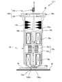
- FIG. 1 schematically shows a configuration of an exposure apparatus according to a first embodiment. It is a figure which takes out one of several photoelectric optical units with which the exposure apparatus of FIG. 1 is equipped, and shows with a part of wafer.
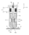
- FIG. 3A is a partially omitted longitudinal sectional view showing a simplified structure of the light beam irradiation apparatus
- FIG. 3B is a bottom view of the light beam irradiation apparatus shown in FIG.
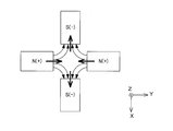
- FIG. 4 is a diagram for explaining the correction of the reduction ratio in the X-axis direction and the Y-axis direction by the first electrostatic lens.
- FIGS. 8A and 8B are diagrams for explaining the correction of the shape change (rounding of four corners) of the cut pattern caused by the optical system-induced blur and the resist blur.
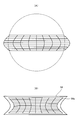
- FIGS. 9A and 9B are diagrams for explaining correction of distortion common to a plurality of electron beam optical systems.
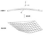
- FIG. 13 is a diagram for explaining a method of compensating the field curvature which the electron beam optical system has as an aberration.
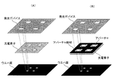
- FIG. 17 (A) is an explanatory view showing a method not using an aperture
- FIG. 17 (B) is an explanatory view showing a method using an aperture.
- FIGS. 18A is a view for explaining an example of the configuration of the separate aperture type photoelectric device
- FIGS. 18B to 18E are views showing various configuration examples of the aperture plate
- FIGS. 19A to 19D are diagrams showing various configuration examples of the aperture integrated photoelectric device. It is a figure which takes out and shows one of 45 photoelectric optical units which comprise the optical system with which the exposure apparatus which concerns on the modification 4 of 1st Embodiment is equipped.
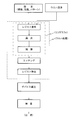
- FIG. 18 is a view for explaining the configuration of a light beam irradiation apparatus that constitutes a part of the photoelectric optical unit of Modification 4; It is a figure for describing one embodiment of a device manufacturing method.
- FIG. 1 schematically shows the structure of an exposure apparatus 100 according to the first embodiment. Since the exposure apparatus 100 is provided with a plurality of electron beam optical systems as described later, hereinafter, the Z axis is parallel to the optical axis of the electron beam optical system, and the exposure will be described later in a plane perpendicular to the Z axis.
- the scanning direction in which the wafer W is moved is taken as the Y-axis direction
- the direction orthogonal to the Z-axis and Y-axis is taken as the X-axis direction
- the rotational (tilting) directions about the X-axis, Y-axis and Z-axis are respectively ⁇ x, ⁇ y
- the description will be made as the and ⁇ z directions.
- the exposure apparatus 100 is supported by a stage chamber 10 installed on a floor surface F of a clean room, a stage system 14 disposed in an exposure chamber 12 inside the stage chamber 10, and a frame 16, and is above the stage system 14. And an optical system 18 disposed at
- the stage chamber 10 is a vacuum chamber capable of evacuating the inside thereof although illustration of both end portions in the X-axis direction is omitted in FIG. 1.
- the stage chamber 10 includes a bottom wall 10a parallel to the XY plane disposed on the floor surface F, the above-described frame 16 which doubles as an upper wall (ceiling wall) of the stage chamber 10, and a periphery of the bottom wall 10a.
- a peripheral wall 10b (only a part of the + Y side portion thereof is shown in FIG. 1) for supporting the frame 16 horizontally from below is provided.
- An opening 16 a is formed in the frame 16.
- the housing 19 of the optical system 18 is disposed in the opening 16a.
- the housing 19 is provided at its upper end portion with a flange portion 19c that protrudes outward beyond the other portions.
- the flange portion 19c of the housing 19 inserted from above into the opening 16a is supported from below on the upper surface of the frame 16 around the opening 16a.
- the optical system 18 is thereby supported by the frame 16.
- a seal member may seal between the inner circumferential surface of the opening 16 a and the outer circumferential surface of the housing 19.
- a stage system 14 is disposed on the bottom wall 10 a of the stage chamber 10.
- the stage system 14 is supported by a platen 22 supported on the bottom wall 10a via a plurality of vibration isolation members 20, and supported by the weight cancellation device 24 on the platen 22 and is predetermined in the X-axis direction and the Y-axis direction.
- the wafer stage WST is movable with a stroke of, for example, 50 mm, and can be finely moved in the remaining four degrees of freedom (Z axis, .theta.x, .theta.y and .theta.z directions), and a stage drive system 26 (FIG. 1 includes only a part of them (see FIG. 6), and a position measurement system 28 (not shown in FIG. 1, see FIG. 6) for measuring positional information in the direction of 6 degrees of freedom of wafer stage WST. .
- Wafer stage WST adsorbs and holds wafer W via an electrostatic chuck (not shown) provided on the upper surface thereof.
- wafer stage WST has a frame-shaped member with an XZ cross section, and mover 30a of motor 30 integrally having a yoke and a magnet (not shown) in the inside (hollow part) thereof.
- a stator 30b of a motor 30 which is fixed and is composed of a coil unit extending in the Y-axis direction is inserted into the inside (hollow portion) of the mover 30a. Both ends of the stator 30 b in the longitudinal direction (Y-axis direction) are connected to an X stage (not shown) that moves on the surface plate 22 in the X-axis direction.
- the X stage has a predetermined stroke in the X axis direction integrally with the wafer stage WST by an X stage drive system 32 (see FIG. 6) configured by a single axis moving mechanism that does not cause magnetic flux leakage, for example, a feed screw mechanism using a ball screw. It is moved by.
- the X stage drive system 32 may be configured by a uniaxial movement mechanism provided with an ultrasonic motor as a drive source. In any case, the influence of the magnetic field fluctuation due to the magnetic flux leakage on the positioning of the electron beam is negligible.
- the motor 30 can move the mover 30a relative to the stator 30b in the Y-axis direction by a predetermined stroke, for example, 50 mm, and can finely move the mover 30a in the X-axis direction, the Z-axis direction, the ⁇ x direction, the ⁇ y direction, and the ⁇ z direction Closed magnetic field type and moving magnet type motor.
- a wafer stage drive system that moves wafer stage WST in the direction of six degrees of freedom by motor 30 is configured.
- the wafer stage drive system will be referred to as wafer stage drive system 30 using the same reference numerals as motor 30.
- the X stage drive system 32 and the wafer stage drive system 30 move the wafer stage WST in the X axis direction and the Y axis direction with a predetermined stroke, for example, 50 mm, and the remaining four degrees of freedom (Z axis, ⁇ x,
- the above-mentioned stage drive system 26 is configured to move slightly in the ⁇ y and ⁇ z directions).
- the X stage drive system 32 and the wafer stage drive system 30 are controlled by the main controller 110 (see FIG. 6).
- Weight cancellation device 24 is a metal bellows type air spring (hereinafter abbreviated as air spring) 24a whose upper end is connected to the lower surface of wafer stage WST, and a flat plate member connected to the lower end of air spring 24a. And a base slider 24b.
- the base slider 24b is provided with a bearing (not shown) for spouting the air inside the air spring 24a to the upper surface of the platen 22, and the bearing surface of the pressurized air ejected from the bearing and the upper surface of the platen 22.
- the weight cancellation device 24, the wafer stage WST (including the mover 30a), and the own weight of the wafer W are supported by the static pressure (pressure in the gap) between them.
- compressed air is supplied to the air spring 24 a through a pipe (not shown) connected to the wafer stage WST.
- the base slider 24b is supported in a non-contact manner on the surface plate 22 via a kind of differential pumping type of static air bearing, and the air ejected toward the surface plate 22 from the bearing portion ) Are prevented from leaking out.
- a pair of pillars are provided sandwiching air spring 24a in the Y-axis direction, and a plate spring provided at the lower end of the pillar is connected to air spring 24a.
- the optical system 18 includes a housing 19 and a plurality of, for example, 45 photoelectro-optical units 17 attached to the housing 19 as shown in FIG. 1.
- a vacuum chamber 33 is formed inside the housing 19.
- the vacuum chamber 33 is, as shown in FIG. 1, a base plate 38 constituting an upper wall (ceiling wall), a cooling plate 74 constituting a bottom wall, and a cylindrical peripheral wall with the cooling plate 74 fixed at its lower end. It is divided by the part 76.
- the housing 19 is configured by fixing the upper end of the peripheral wall portion 76 to the lower surface of the base plate 38.
- the cooling plate 74 of the present embodiment has a cooling function, but may have a function of suppressing fogging described later in addition to the cooling function.
- the plate 74 may not have a cooling function.
- a plurality of through holes 38a extending in the Z-axis direction are provided at predetermined intervals in the XY two-dimensional direction.
- a light beam irradiation device 80 described later is disposed with almost no gap.
- a seal member may be disposed between the light beam irradiation device 80 and the through hole 38a. Further, the light beam irradiation device 80 may be installed on the lower surface of the base plate 38 without providing the through hole in the base plate 38.
- FIG. 2 shows the photoelectric optical unit 17 viewed from the + X direction.
- the photoelectric optical unit 17 includes a light beam irradiation device 80 attached to a base plate 38 and an electron beam optical system 70.
- the structure of the light beam irradiation apparatus 80 is simplified and shown by FIG. 3 (A).
- the light beam irradiation apparatus 80 is one in which a light emitting device 84 for generating light and a photoelectric element 54 are integrated.
- the light beam irradiation apparatus also includes a type including a light emitting device and a photoelectric element separated from the light emitting device as in the first to third modified examples described later, like the light beam irradiation apparatus 80, A light beam irradiation apparatus of a type in which the light emitting device 84 and the photoelectric device 54 are integrated may be called a photoelectric device in a broad sense.
- a light emitting device mainly composed of a self light emitting contrast device array is used as the light emitting device 84. Therefore, in the following, also with the self light emitting contrast device array 84 using the same reference numerals as the light emitting device 84. It is called.
- a light emitting device 84 ie, a self light emitting contrast device array 84, is a programmable patterning device built in a semiconductor substrate, arranged in a one or two dimensional array, and having a plurality of individually controllable light emitting portions is there.
- the self-luminous contrast device array 84 is formed, for example, by laminating a plurality of compound semiconductor constituent material layers on a substrate, and then selectively removing each compound semiconductor constituent material layer by wet etching to obtain each light emitting element
- the semiconductor layer of part (1) is formed into a mesa structure, or the light emitting elements are separated.
- the light emitting device 84 includes, for example, a pn junction of a semiconductor with a double hetero junction (structure), and the light emitting portion 84 a and the plurality of light emitting portions 84 a arranged individually in an XY two-dimensional array on the semiconductor substrate. And a plurality of CMOS drive circuits 84b to be driven.
- a micro LED which is a type of self-luminous contrast device, is used as the plurality of light emitting portions 84a, so in the following, the micro LED 84a is denoted using the same reference numeral as the light emitting portion. .
- the CMOS drive circuit 84b is simplified and shown as a simple transistor.
- reference numeral 85 schematically shows interconnections connected to the plurality of CMOS drive circuits 84b.
- a plurality of micro LEDs manufactured in advance may be arranged on the substrate and used as the light emitting device 84.
- the light emitting device 84 can individually control the intensity of the light beam LB from each of the plurality of micro LEDs 84a by controlling the voltage applied thereto, and the intensity is controlled to zero, that is, the light beam LB Light emission stop.
- the light emitting device 84 may be said to generate an optical pattern consisting of, for example, a light and dark pattern.
- the photoelectric element 54 is disposed on the emission surface side of the plurality of micro LEDs 84 a of the light emitting device 84, and is a plate-like light transmission member, for example, quartz glass capable of transmitting the plurality of beams LB emitted from the micro LEDs 84 a without passing through space.
- Plate member 56 a light shielding film (aperture film) 58 made of chromium or the like deposited on the lower surface of the plate member 56, an alkaline photoelectric film (photoelectric film formed on the lower surface side of the plate member 56 and the light shielding film 58) And a layer (alkali photoelectric conversion layer (alkali photoelectric layer)) 60 of the conversion film).
- the material of the plate member 56 is not limited to quartz glass, and may be, for example, a material having transparency to the wavelength of light (beam) emitted by the micro LED 84 a such as sapphire.
- the light beam irradiation device 80 is shown in FIG. 3A, in practice, a large number of apertures 58a are formed in the light shielding film 58 in a predetermined positional relationship (see FIG. 3A). 3 (B)).
- the alkaline photoelectric layer 60 is also disposed inside the aperture 58a, and the plate member 56 and the alkaline photoelectric layer 60 are in contact with each other at the aperture 58a.
- the plate member 56, the light shielding film 58, and the alkaline photoelectric layer 60 are integrally formed, and at least a part of the photoelectric element 54 is formed.
- the micro LEDs 84 a which are a plurality of light emitting portions of the light emitting device 84 and the plurality of CMOS drive circuits 84 b are further integrally formed with the photoelectric element 54 by a semiconductor process.
- the CMOS drive circuit 84b is fabricated on a silicon substrate, and the micro LED has a PN junction structure of, for example, gallium nitride (GaN).
- GaN gallium nitride
- the light emitting device 84 and the photoelectric element 54 may be joined after the light emitting device 84 and the photoelectric element 54 are separately formed. In this case, a member or a film that transmits the light beam from the light emitting device 84 may be disposed between the light emitting device 84 and the photoelectric element 54.
- the plurality of micro LEDs 84a and the apertures 58a correspond one to one. That is, the arrangement of the apertures 58a on one surface (light emitting surface) of the plate member 56 corresponds to the arrangement of the micro LEDs 84a on the other surface (light incident surface) of the plate member 56.
- the light emitting portion is not limited to the micro LED, and other radiation emitting diodes such as a light emitting diode, an organic LED, a polymer LED, a laser diode and the like can also be used.
- the light emitting portion is not limited to the radiation emitting diode, but may be another self-emitting contrast device such as a vertical cavity surface emitting laser (VCSEL) or a vertical external cavity surface emitting laser (VECSEL).
- VCSEL vertical cavity surface emitting laser
- VECSEL vertical external cavity surface emitting laser
- These light emitting units emit light beams in a direction perpendicular to the semiconductor substrate, ie, in a direction perpendicular to the surface of the plate member 56. Therefore, the light emitting units in FIG. 3A (self-luminous contrast device) As the light source 84a, these light emitting units can be used instead of the micro LED.
- the alkali photoelectric layer 60 is a multi-alkali photocathode using two or more types of alkali metals.
- the multialkali photocathode is a photocathode characterized by high durability, capable of generating electrons with green light having a wavelength of 500 nm band, and high quantum efficiency QE of the photoelectric effect of about 10%.
- the alkaline photoelectric layer 60 is used as a kind of electron gun that generates an electron beam by the photoelectric effect of laser light (also called a laser beam or a light beam), the conversion efficiency is 10 mA / W. High efficiency is used.
- the electron emission surface of the alkaline photoelectric layer 60 is the surface opposite to the lower surface in FIG. 3A, that is, the surface on the side facing the plate member 56.
- each of the plurality of micro LEDs 84a it is possible to irradiate the corresponding aperture 58a via the plate member 56 with a light beam LB (hereinafter, suitably abbreviated as beam LB) having a cross section larger than the corresponding aperture 58a.
- beam LB a light beam LB
- the beam LB is emitted to the alkaline photoelectric layer (hereinafter abbreviated as a photoelectric layer) 60 through the aperture 58a, and an electron beam EB having a cross section corresponding to the shape of the aperture 58a is converted from the photoelectric layer 60 by photoelectric conversion. It is ejected in the Z direction.
- the photoelectric element 54 is disposed on the emission surface side of the plurality of micro LEDs 84 a of the light emitting device array 84, and the photoelectric layer 60 is also disposed inside the aperture 58 a.
- the beam LB can be applied to the photoelectric layer 60 through the gas space (the space in which the gas is present) and the corresponding aperture 58a without passing through the vacuum space.
- the photoelectric device 54 of the present embodiment can irradiate the beam LB from each of the plurality of micro LEDs 84 a to the photoelectric layer 60 via the corresponding aperture 58 a without passing through the vacuum space.
- the present invention is not limited thereto, and a space (one or both of the gas space and the vacuum space) through which the light beam LB can pass may be formed between each of the plurality of micro LEDs 84 a and the photoelectric layer 60. .
- 72000 apertures 58 a are formed in the light shielding film 58 of the photoelectric element 54 so that the 72000 light beams generated by the light emitting device 84 can be individually irradiated. Note that the number of apertures 58a need not be the same as the number of light beams that can be emitted by the light emitting device 84, for example.
- the photoelectric elements 54 shields the light
- the photoelectric elements 54 include apertures 58a to which 72000 beams (laser beams) correspond. It suffices to irradiate the region on the film 58). That is, the size of each of the plurality of apertures 58a on the photoelectric element 54 may be smaller than the size of the cross section of the corresponding beam.
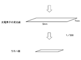
- 72000 beams have a length of S mm in the X-axis direction and a length of T mm in the Y-axis direction on the light receiving surface of the photoelectric element 54 (the surface on which the multiple apertures 58a are formed). The rectangular area is irradiated.
- the plurality of apertures may be irradiated with one light beam (for example, light beam from one micro LED). In this case, switching of the light beam incident on the photoelectric layer 60 is performed for each of the plurality of apertures.
- the number of apertures 58a may be the same as the number of multi-electron beams described later, or may be larger than the number of multi-electron beams.
- the electron beam optical system 70 includes a lens barrel 104 whose upper end is connected to the lower surface of the base plate 38, and an objective lens consisting of a pair of electromagnetic lenses 70a and 70b held by the lens barrel 104. , Electrostatic multipole 70c.
- the objective lens of the electron beam optical system 70 and the electrostatic multipole 70 c irradiate a plurality of beams LB to the photoelectric element 54 to emit (emit) electrons (electron beam EB) from the photoelectric layer 60 by photoelectric conversion. It is located on the beam path.
- the pair of electromagnetic lenses 70a and 70b are disposed in the vicinity of the upper end and the lower end in the lens barrel 104, respectively, and they are separated in the vertical direction.
- an extraction electrode 112 for accelerating electrons emitted from the photoelectric layer 60 is disposed.
- the electromagnetic lenses 70 a and 70 b may be disposed outside the lens barrel 104.
- An electrostatic multipole 70c is disposed between the pair of electromagnetic lenses 70a and 70b.
- the electrostatic multipole 70c is disposed near the beam waist on the beam path of the electron beam EB focused by the objective lens. For this reason, the plurality of beams EB passing through the electrostatic multipole 70c may repel each other by the coulomb force acting between them, and the magnification may change.
- a first electrostatic lens 70c 1 for XY magnification correction, the irradiation position control of the beam (and the irradiation position shift correction), i.e. the projection position adjustment of the optical pattern produced by the light emitting device 84 (and An electrostatic multipole 70 c having a second electrostatic lens 70 c 2 for correction of projection position shift) is provided inside the electron beam optical system 70.
- each of the first electrostatic lens 70c 1 and the second electrostatic lens 70c 2 is, irradiation position control of the XY magnification correction and the electron beam (and the irradiation position shift correction) may be performed.
- the electrostatic lens 70c 1 may be allowed to the axial direction of the magnification adjustment different from the X-axis direction and the Y-axis direction. Further, it may be omitted first electrostatic lens 70c 1 and one of the second electrostatic lens 70c 2, an electrostatic multipole 70c may also have additional electrostatic lenses.
- the second electrostatic lens 70c 2 corrects the irradiation position displacement of the beam due to various vibrations and the like (the projection position shift of the cut pattern to be described later) at once.
- the second electrostatic lens 70c 2 is deflection control of the beam for performing the following control for the wafer W of the beam during exposure, i.e., it is also used for the irradiation position control of the beam.
- the reduction magnification of the electron beam optical system 70 is, for example, 1/200 in design without performing magnification correction.
- Other magnifications such as 1/120 and 1/80 may be used.
- a plurality of, here, 45 electron beam optical systems 70 are supported by the base plate 38 in a suspended state.
- an exit 104a of the electron beam is formed at the exit end of the lens barrel 104, and the backscattered electron detection device 106 is disposed below the exit 104a.
- the backscattered electron detection device 106 is disposed inside a circular (or rectangular) opening 74 a formed in the cooling plate 74 so as to face the above-described outlet 104 a. More specifically, a pair of backscattered electron detectors 106y 1 and 106y 2 are provided on both sides in the Y-axis direction with respect to the optical axis AXe of the electron beam optical system 70.
- a pair of backscattered electron detectors 106 x 1 and 106 x 2 are provided on both sides in the X-axis direction with respect to the optical axis AXe (see FIG. 6).
- Each of the two pairs of backscattered electron detection devices 106 is formed of, for example, a semiconductor detector, and detects and detects a reflected component generated from a detection target mark such as an alignment mark or a reference mark on a wafer.
- a detection signal corresponding to the reflected electrons is sent to the signal processing unit 108 (see FIG. 6).
- the signal processing unit 108 amplifies the detection signals of the plurality of backscattered electron detection units 106 by an amplifier (not shown) and then performs signal processing, and sends the processing result to the main control unit 110 (see FIG. 6).
- the backscattered electron detection device 106 may or may not be provided only on a part (at least one) of the 45 electron beam optical systems 70.
- the backscattered electron detectors 106 x 1 , 106 x 2 , 106 y 1 , 106 y 2 may be fixed to the lens barrel 104 or may be attached to the cooling plate 74.
- the cooling plate 74 45 openings 74a are individually formed facing the exit 104a of the lens barrel 104 of the 45 electron beam optical system 70, and two pairs of the backscattered electron detecting devices 106 are disposed in the opening 74a. It is done. Note that the exposure apparatus 100 may not include the backscattered electron detection device 106. Further, the exposure apparatus 100 may not be provided with a cooling plate.
- the internal space of the lens barrel 104 is also a vacuum space so that the photoelectric layer 60 is not exposed to the atmosphere.
- the internal space of the lens barrel 104 may be a high vacuum space as compared to the vacuum chamber 33 outside thereof. In this case, the evacuation of the vacuum chamber 33 and the evacuation of the lens barrel 104 may be performed separately.
- the optical system 18 is assembled in a vacuum chamber in a high vacuum state installed inside a clean room in an exposure apparatus manufacturer's factory. At that time, the components of the optical system 18 excluding the light beam irradiation device 80 are carried in the vacuum chamber in a pre-assembled state, and 45 light beam irradiation devices 80 are arranged in the through hole 38 a of the base plate 38. After being inserted into the interior and the position is finely adjusted, the gap between the through hole 38 a and the light beam irradiation device 80 is sealed, thereby completing the assembly of the optical system 18.
- each of the 45 lens barrels 104 is airtight with respect to the outside, and the state of high vacuum inside can be maintained.
- the inside of the vacuum chamber 33 is also in a high vacuum state, it is desirable to temporarily close the opening 74 a of the cooling plate 74 by attaching a seal member or the like.
- the assembled optical system 18 is carried out of the vacuum chamber to the outside (in the clean room), then inserted from above into the opening 16 a of the frame 16 in the clean room, and assembled to the frame 16. In this assembled state, almost no gap exists between the housing 19 and the opening 16 a of the frame 16.
- the 45 openings 74 a formed in the cooling plate 74 are temporarily closed.
- the vacuum of the inside of the housing 19 is a stage chamber. 10 It is done in parallel with the vacuum inside.
- each of the plurality of light beam irradiation devices 80 functions as a partition (vacuum partition) that separates at least a part of the light emitting device 84 that each has from the vacuum chamber 33 and the space outside the vacuum chamber 33 (the outside of the housing 19). doing.
- the outside of the vacuum chamber 33 is at atmospheric pressure, or slightly positive pressure than atmospheric pressure.
- the inside of the stage chamber 10 is evacuated until a medium vacuum state where the degree of vacuum is low (high air pressure) compared to the vacuum chamber 33 is achieved. Thereafter, the necessary adjustments for the optical system 18 are made.
- the necessary adjustment of each part mentioned above includes adjustment for achieving optical accuracy for various optical systems, adjustment for achieving mechanical accuracy for various mechanical systems, and electrical accuracy for various electric systems. Adjustments to achieve are included.
- the length S mm in the X-axis direction on the light receiving surface of the light emitting device 84 from the light emitting device 84 The beam is irradiated inside a rectangular area of length T mm in the Y-axis direction, and the electron beam generated by this irradiation passes through the electron beam optical system 70 having a reduction ratio of 1/200 to the image plane (image plane Is illuminated onto a rectangular area (exposure field) on the wafer surface).
- the light beam irradiation apparatus 80 (including the light emitting device 84 and the photoelectric element 54 integrated therewith) and the electron beam optical system 70 corresponding to the light beam irradiation apparatus 80
- a direct cylindrical multi-beam optical system 200 (see FIG. 6) having a reduction ratio of 1/200 is configured, and the multi-beam optical system 200 is arranged in the above-described matrix arrangement 45 in the XY plane. . Therefore, the optical system of the exposure apparatus 100 of the present embodiment is a multi-column electron beam optical system having 45 reduction optical systems with a reduction ratio of 1/200.
- the exposure apparatus 100 for example, a wafer with a diameter of 300 mm is to be exposed, and 45 electron beam optical systems 70 are disposed to face the wafer. It is 43 mm.
- the exposure area handled by one electron beam optical system 70 is a rectangular area of 43 mm ⁇ 43 mm at maximum, so as described above, the movement stroke of wafer stage WST in the X-axis direction and Y-axis direction is 50 mm is enough.
- the number of electron beam optical systems 70 is not limited to 45, and can be determined based on the diameter of the wafer, the stroke of the wafer stage WST, and the like.
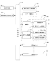
- FIG. 6 is a block diagram showing the input / output relationship of the main controller 110 that mainly constitutes the control system of the exposure apparatus 100.
- Main controller 110 centrally controls components of exposure apparatus 100 including a microcomputer and the like shown in FIG.
- the light beam irradiation device 80 connected to the control unit 11 includes a light emitting device controlled by the control unit 11 based on an instruction from the main control unit 110, that is, a self light emitting contrast device array 84.
- the electron beam optical system 70 connected to the control unit 11 is a pair of electromagnetic lenses 70 a and 70 b and electrostatic multipoles 70 c controlled by the control unit 11 based on an instruction from the main control device 110 (first The electrostatic lens 70 c 1 and the second electrostatic lens 70 c 2 ) are included.
- reference numeral 500 denotes an exposure unit configured to include the multi-beam optical system 200 described above, the control unit 11, and the signal processing device 108. In the exposure apparatus 100, an exposure unit 500 is provided.
- the exposure apparatus 100 adopts a rectangular (rectangular) exposure field instead of a square for the following reason.
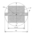
- FIG. 7 a square field SF and a rectangular field RF are shown in a circle indicating the effective area (aberration effective area) of the diameter D of the electron beam optical system.
- the square field SF is preferable to maximize the effective area of the electron beam optical system.
- the field width is lost by about 30% (1 / ⁇ 2).
- the effective area is almost the field width. This is a great advantage for multi-columns.
- the rectangular field has a higher current density than the square field, since the total amount of electrons irradiated in the field is the same, so even if the mark is placed in a smaller area on the wafer It can detect with sufficient detection sensitivity. Also, rectangular fields are easier to manage as compared to square fields.
- the practical aspect ratio a / b is 1/12 to 1/4.
- both the square field SF and the rectangular field RF exposure field are set to include the optical axis AXe of the electron beam optical system.
- the exposure field may be set within the aberration effective area so as not to include the optical axis AXe.
- the exposure field may be set to a shape other than a rectangle (including a square), for example, an arc.
- Irradiance unevenness in the exposure field is performed on the electron emission surface of the photoelectric layer 60 as a result of the main controller 110 performing intensity control of the light beam by controlling the applied voltage at the time of exposure to be described later. Adjustment of the illuminance distribution in the surface of the light source and the corresponding illuminance distribution in the exposure field RF on the wafer surface, that is, dose control. That is, the intensities of the plurality of electron beams irradiated to the exposure field RF are properly adjusted.
- the intensities of the plurality of electron beams generated from the electron emission surface of the photoelectric layer 60 by photoelectric conversion is performed so that the amount of current
- the beam intensity (the illuminance of the electron beam, the beam current amount) of at least a part of the plurality of electron beams generated from the electron emission surface of the photoelectric layer 60 by photoelectric conversion is made different from the intensities of the other beams.
- the intensity of a plurality of beams irradiated to the photoelectric layer 60 may be adjusted.
- the resist layer formed on the wafer is not affected only by the in-plane illuminance distribution on the electron emission surface of the photoelectric layer 60, and other factors such as forward scattering, back scattering, or fogging of electrons And so on.
- forward scattering refers to a phenomenon in which electrons incident on the inside of the resist layer on the wafer surface are scattered in the resist layer before reaching the wafer surface
- back scattering refers to the wafer via the resist layer. It means that the electrons reaching the surface are scattered at or inside the wafer surface, re-incident in the resist layer, and scattered around.
- “fogging” refers to a phenomenon in which reflected electrons from the surface of the resist layer are re-reflected on the bottom surface of the cooling plate 74, for example, and a dose is applied to the periphery.
- exposure apparatus 100 adopts different correction methods for forward scattering and backscattering and fogging. ing.
- the main controller 110 estimates the in-plane illuminance distribution using the light emitting device 84 through the control unit 11 in anticipation of the influence of the forward scattering component. Make adjustments for
- the main controller 110 controls the control unit 11 to set the surface at a certain spatial frequency. It is necessary to adjust the illuminance distribution inside.
- the exposure apparatus 100 is used, for example, in complementary lithography.
- a wafer on which an L / S pattern is formed is used as an exposure target by using double patterning or the like in immersion exposure using an ArF light source, and is used for forming a cut pattern for cutting the line pattern.
- Be In the exposure apparatus 100 it is possible to form a cut pattern corresponding to each of 72000 apertures 58a formed in the light shielding film 58 of the photoelectric element 54.
- the flow of processing on a wafer in the present embodiment is as follows.
- the wafer W before exposure to which the electron beam resist has been applied is placed on the wafer stage WST in the stage chamber 10 and is attracted by the electrostatic chuck.
- Electrons from each electron beam optical system 70 for at least one alignment mark formed on a scribe line (street line) corresponding to each of, for example, 45 shot areas formed on wafer W on wafer stage WST The beam is irradiated, and the backscattered electrons from at least one alignment mark are detected by at least one of backscattered electron detectors 106 x 1 , 106 x 2 , 106 y 1 , 106 y 2 , and all-point alignment measurement of wafer W is performed. Based on the result of the all-point alignment measurement, exposure using 45 exposure units 500 (multi-beam optical system 200) is started on 45 shot areas on the wafer W.
- 45 exposure units 500 multi-beam optical system 200
- the irradiation timing (on / off) of each beam is controlled while scanning the wafer W (wafer stage WST) in the Y-axis direction.
- alignment marks formed corresponding to a part of the shot areas of the wafer W may be detected without performing the all-point alignment measurement, and 45 shot areas may be exposed based on the detection result.
- the number of exposure units 500 and the number of shot areas are the same, but may be different. For example, the number of exposure units 500 may be smaller than the number of shot areas.
- the alignment mark may be detected outside the stage chamber 10. In this case, it is not necessary to detect the alignment mark in the stage chamber 10.
- the self-luminous contrast device array (light emitting device) 84 includes 6000 micro LEDs arranged at a predetermined pitch in the X-axis direction, and arranged in the Y-axis direction at a predetermined pitch A, B, C,. , K, L columns of twelve micro LEDs (referred to as LED columns) are provided.
- the exposure using the LED column A is started on a continuous 6000 pixel region of a certain row (referred to as a Pth row) aligned in the X-axis direction on the wafer.
- a Pth row a continuous 6000 pixel region of a certain row aligned in the X-axis direction on the wafer.
- the beam from the LED array A (more precisely, the electron beam corresponding to the light beam emitted from the LED array A) is at the home position.
- the exposure to the same 6000 pixel region is continued while deflecting the beam in the + Y direction (or -Y direction) by making the scan of the wafer W in the + Y direction (or -Y direction) from the start of exposure follow.
- wafer stage WST advances at a velocity V [nm / s], for example Ta x V [nm].
- V [nm / s] for example Ta x V [nm].
- Ta ⁇ V 96 [nm].
- the beam is returned to the home position while the wafer stage WST scans at 24 nm in the + Y direction at a velocity V. At this time, the beam is turned off (the intensity is zero) so that the resist on the wafer is not actually exposed.
- the continuous 6000 pixel area on the (P + 12) th line has the same position as the 6000 pixel area on the Pth line at the exposure start time. It is in.
- the continuous (6000 pixel area) on the (P + 12) th row is exposed while deflecting the beam to the wafer stage WST.
- the self-luminous contrast device array A cut pattern can be formed by turning on any micro LED among the 72000 micro LEDs at 84. In this case, 72000 beams may or may not be simultaneously irradiated on the wafer.
- main scanning drive 110 controls stage drive system 26 based on the measurement values of position measurement system 28 during scanning exposure to wafer W based on the above-described exposure sequence.
- the light beam irradiation device 80 and the electron beam optical system 70 are controlled via the control unit 11 of each exposure unit 500.
- the control unit 11 performs the above-described dose control as necessary.
- the dose control described above is dose control performed by controlling the light emitting element, that is, the self-emission type contrast device array 84, it can be said that it is dynamic dose control.
- the exposure apparatus 100 is not limited to this, and the following dose control can also be adopted.
- a cut pattern (resist pattern) CP that should be originally square (or rectangular) on the wafer is, for example, 4 as shown in FIG. A corner may be rounded to look like a cut pattern CP '.
- a light beam is photoelectrically transferred through a non-rectangular aperture 58a 'in which auxiliary patterns 58c are provided at four corners of the aperture 58a formed in the light shielding film 58.
- an electron beam generated by photoelectric conversion is irradiated onto the wafer through the electron beam optical system 70 to form an irradiation area of the electron beam having a shape different from that of the non-rectangular aperture 58a 'on the wafer.
- the shape of the irradiation area of the electron beam and the shape of the cut pattern CP to be formed on the wafer may be the same or different.
- the shape of the aperture 58a ' is set so that the shape of the electron beam irradiation area is substantially the same as the shape of the desired cut pattern CP (for example, rectangular or square). You should decide. Use of the aperture 58a 'in this case may not be considered as dose control.
- the auxiliary pattern 58c need not be provided at all four corners of the rectangular aperture 58a, and the auxiliary pattern 58c may be provided at at least a part of the four corners of the aperture 58a. Further, the auxiliary pattern 58c may be provided at all four corners of the rectangular aperture 58a only in a part of the plurality of apertures 58a 'formed in the light shielding film 58. Further, some of the plurality of apertures formed in the light shielding film 58 may be the apertures 58a ', and the remaining may be the apertures 58a. That is, it is not necessary to make all the shapes of the plurality of apertures 58a 'formed in the light shielding film 58 the same.
- the shape, size, etc. of the aperture is optimized based on, for example, the characteristics of the electron beam optical system 70 based on the actual exposure result. Is desirable.
- the shape of each aperture is determined so as to suppress rounding of the corner of the irradiation area on the wafer (target). The influence of the forward scattering component can also be reduced by the aperture shape.
- the shape of the aperture 58a ' may be the same as the shape of the irradiation region of the electron beam.
- the exposure apparatus 100 has a plurality of electron beam optical systems 70, for example 45, but the 45 electron beam optical systems 70 are manufactured through the same manufacturing process so as to satisfy the same specifications.
- inherent distortion disortion aberration
- the distortion common to the plurality of electron beam optical systems 70 cancels the distortion of the arrangement of the apertures 58a on the light shielding film 58 located on the photoelectric layer 60, as schematically shown in FIG. 9B.
- the correction may be made in such an arrangement as to reduce or reduce.
- the circle in FIG. 9A indicates the aberration effective area of the electron beam optical system 70.
- each aperture 58a is shown not as a rectangle but as a parallelogram etc. for clarity in FIG. 9 (B), the aperture 58a on the light shielding film 58 is actually formed with a rectangle or a square. Be done.
- This example shows a case where barrel distortion inherent to the electron beam optical system 70 is canceled or reduced by arranging a plurality of apertures 58a on the photoelectric layer 60 along the pincushion distortion shape.
- the distortion of the electron beam optical system 70 is not limited to the barrel distortion, and, for example, when the distortion of the electron beam optical system 70 is a pincushion distortion, a plurality of apertures are provided to cancel or reduce the influence.
- 58a may be arranged in a barrel distortion shape.
- the adjustment may not be performed when the light beam can be irradiated to the area including each aperture 58a.
- the exposure apparatus 100 includes the exposure unit 500 configured to include the multi-beam optical system 200, the control unit 11, and the signal processing device 108 (see FIG. 6).
- the multi-beam optical system 200 includes a light beam irradiation apparatus 80 and an electron beam optical system 70.
- the light beam irradiation apparatus 80 has a plurality of light sources that can be individually controlled, for example, a micro LED 84a, and can emit light beams from the light emitting device 84 capable of providing a plurality of light beams; And the photoelectric element 54 having the photoelectric layer 60 irradiated without passing through the vacuum space (or both of them), and the electron beam optical system 70 irradiates the photoelectric element 54 with a plurality of light beams to obtain the photoelectric element The electrons emitted from the electron beam 54 are irradiated to the wafer W as a plurality of electron beams.
- the exposure apparatus 100 since there is no blanking aperture, the source of generation of complex distortion due to charge-up and magnetization is fundamentally eliminated and waste electrons (reflected electrons) not contributing to the exposure of the target are reduced. It will be possible to eliminate long-term instability factors. In addition to this, switching between electron beam irradiation and non-irradiation states on the target, that is, switching function of turning on and off the electron beam, is realized without using moving parts that inevitably deteriorate with time. Because you can, the benefits are great. In addition, unlike the case where a beam switching function is realized using a movable part, an illumination optical system other than the electron beam optical system, a projection optical system, etc.
- the plurality of light emitting units (micro LEDs) 84a each capable of providing the light beam (laser beam) LB and the plurality of laser beams LB by the light emission of the plurality of light emitting units 84a.
- the electron beam optical system 70 capable of irradiating the wafer W serving as the target with electrons emitted from the photoelectric layer 60 by irradiating the photoelectric layer 60 with the plurality of light emitting portions 84 a
- Each of the laser beams is incident on the photoelectric layer 60 without passing through space.
- the light emitting portion 84a has a wavelength with a small amount of absorption by gas molecules (present in a part of visible to infrared region It becomes possible to use radiation sources emitting laser light of other wavelengths as well as called), ie self-emitting contrast devices. By appropriately selecting the wavelength, it is possible to perform photoelectric conversion using the laser beam LB efficiently and to irradiate the wafer W with the high energy electron beam EB.
- main controller 110 performs scanning (movement) of wafer stage WST holding wafer W in the Y-axis direction via stage drive system 26. Control.
- the main control unit 110 passes n (for example, 72000) apertures 58 a of the photoelectric element 54 for each of the m (for example, 45) multi-beam optical systems 200 of the exposure unit 500.
- the irradiation state (on state and off state) of the n beams is changed for each aperture 58a, and the intensity adjustment of the light beam is performed for each beam using the self-emission type contrast device array (light emitting device) 84.
- the first electrostatic lens 70c 1 of the electrostatic multipole 70c caused by changes in the total current amount, reduction in the X-axis direction and the Y-axis direction due to the Coulomb effect magnification (changes in) Correct, fast, and individually.
- the second electrostatic lens 70c 2 correction (light pixels of the optical pattern, i.e. the projection position deviation of the cut pattern to be described later) irradiation position shift of the beam caused by various vibrations or the like in a batch Do.
- a fine line and space pattern in which the X axis direction formed in advance in each of, for example, 45 shot areas on the wafer by double patterning using an ArF immersion exposure apparatus, for example, It becomes possible to form a cut pattern at a desired position on a desired line of the pattern), and high precision and high throughput exposure is possible.
- any of the plurality of apertures 58 a in each multi-beam optical system 200 Even when the beam passing through the aperture 58a is in the on state, in other words, regardless of the combination of the beams in the on state, X formed in advance on each of, for example, 45 shot areas on the wafer It becomes possible to form a cut pattern at a desired position on a desired line of a fine line and space pattern in which the axial direction is a periodic direction.
- a self-emission contrast device array having 13 LED rows may be used instead of the self-emission contrast device array 84 having 12 LED rows.
- the 13th LED row is a backup LED row that is used in place of the LED row in which a defect has occurred when any of the 12 commonly used LED rows (main LED rows) has a defect. It is.
- a plurality of backup LED strings may be provided.
- An array of apertures may be provided.
- the light beam irradiation device 80 is described as being integrally formed with the light emitting device (self light emitting contrast device array) 84 and the photoelectric element 54 by the semiconductor process, but the present invention is not limited thereto.
- a separate light beam irradiator 180 may be used, which includes a light emitting device 184 and a photoelectric element 136 which is separate from the light emitting device 184 and is disposed apart from the light emitting device.
- the light emitting device 184 is provided with a microlens array 84c, which is a type of optical element, on the light emitting side of the self-luminous contrast device array 84 described above.
- the microlens array 84c is provided corresponding to each of a plurality of light emitting portions, here, the micro LEDs 84a which is a type of self-luminous contrast device, and crosses each other in the XY plane corresponding to the arrangement of the plurality of micro LEDs 84a. And a plurality of microlenses (optical members, optical elements) disposed and integrated in a two-dimensional array in two directions (for example, the X-axis direction and the Y-axis direction).
- the microlens array 84c condenses the diverging light generated by the corresponding micro LED 84a and converts it into parallel light.
- the optical element provided in the light emitting device 184 is not limited to the refractive optical element, and may be a diffractive optical element, a reflective optical element, or a combination thereof.
- FIG. 11 shows one of 45 photo-optical units 117 constituting the optical system 18 provided in the exposure apparatus according to the first modification.
- the photoelectric optical unit 117 differs from the photoelectric optical unit 17 described above in that a light emitting device 184 is inserted into the through hole 38 a of the base plate 38 instead of the light beam irradiation device 80 described above.
- the light emitting device 184 doubles as a vacuum partition that separates the inside and the outside of the lens barrel 104 from each other.
- the photoelectric element 136 is disposed below the microlens array 84c of the light emitting device 184 via a predetermined clearance (gap, clearance).
- the light emitting device 184 may be installed on the lower surface of the base plate 38 or the like without providing the through holes 38 a in the base plate 38.
- the photoelectric device 136 has a base 134 made of a light transmitting member, a light shielding film 58 having a large number of apertures 58a formed on the lower surface (light emitting surface) thereof, a base 134 and a light shielding It has the photoelectric layer 60 formed on the lower surface of the film 58, and is configured in the same manner as the photoelectric device 54 described above.
- the exposure apparatus according to the modification 1 is the same as the exposure apparatus according to the first embodiment described above in the configuration of the other parts of the photo-optical unit 117 and the configuration other than the photo-optical unit 117.
- the photoelectric element 136 may be supported at a predetermined position inside the lens barrel 104 by a support member (not shown), but adopts a configuration movable in the XY plane by a vacuum compatible actuator (not shown). Also good. In the latter case, each micro LED 84 a of the light emitting device 184 may correspond to the aperture 58 a of the photoelectric element 136 at one to one. However, the invention is not limited thereto, and the number of micro LEDs 84 a and the number of apertures 58 a may be different. You may That is, more apertures 58a may be formed in the light shielding film 58 than the micro LEDs 84a, or fewer apertures 58a may be formed in the light shielding film 58 than the micro LEDs 84a.
- the light shielding film 58 of the photoelectric element 136 may be formed with a smaller number of rows of apertures 58a than the number of rows of the micro LEDs 84a.
- at least one row of the row of micro LEDs 84a may be a backup LED row.
- a target area (referred to as a first target area) on the wafer which is a target, and included, for example, in one micro LED 84a included in the backup LED array or in another LED array of the main LED array
- the electron beam generated by irradiating the photoelectric device 136 with the light beam from one of the micro LEDs 84 a may be configured to be able to irradiate the first target area on the wafer. That is, the electron beams generated by the photoelectric element 136 due to the irradiation of the light beams from the two micro LEDs 84a respectively contained in different LED strings may be overlapped and irradiated onto the same target area on the wafer. By this, for example, the dose amount of the target region may be in a desired state.
- the light shielding film 58 of the photoelectric element 136 may be formed with a row of apertures 58 a in a number greater than the number of rows of the micro LEDs 84 a.
- at least one row of the rows of the apertures 58a may be a row of apertures for backup.
- the light beams LB generated by the plurality of light emitting units 84 a of the light emitting device 184 enter the corresponding microlens without passing through space, are converted into parallel light, and are vacuumed.
- the light is irradiated to the base material 134 of the photoelectric element 136 through the space, and the photoelectric layer 60 is irradiated through any of the apertures 58a. That is, in the exposure apparatus according to the first modification, the light beam LB generated by the plurality of light emitting units 84 a of the light emitting device 184 is irradiated to the photoelectric layer 60 without passing through the gas space.
- the field curvature component of the electron beam optical system becomes noticeable.
- the photoelectric layer 60 (correctly, the entire photoelectric element 136)
- the light emitting layer 60 may be bent such that a curve having an opposite phase to the curvature component of the image plane is generated in the photoelectric layer 60, that is, the electron emission surface of the photoelectric layer 60 may be curved (nonplanar).
- the amount of curvature of the electron emission surface of the photoelectric layer 60 may be variable.
- the amount of curvature of the electron emission surface may be changed according to a change in optical characteristics (aberration, for example, curvature of field) of the electron beam optical system 70. Therefore, the amount of curvature of the electron emission surface may be made different among the plurality of photoelectric elements 136 according to the optical characteristics of the corresponding electron beam optical system 70 respectively. Further, FIG.
- the photoelectric element 136 (photoelectric layer 60) is not limited to bending in one direction, but may of course be deformed three-dimensionally such as bending four corners downward.
- the position of the portion (for example, the central portion) of the electron emitting surface and the other portion (for example, the peripheral portion) with respect to the direction of the optical axis AXe It will be different from each other.
- the thickness of the photoelectric layer 60 may have a distribution so that the positions of a part (for example, the central part) of the electron emission surface and the other part (for example, the peripheral part) in the direction of the optical axis AXe may be different. Even when the light emitting device 84 and the photoelectric element 54 are integrally formed, the electron emission surface may be curved.
- the photoelectric element 136 is a so-called aperture-integrated photoelectric element in which an aperture is integrally provided with the photoelectric layer similarly to the photoelectric element 54, but, for example, when the actuator can be moved in the XY plane by an actuator, As shown in FIG. 14, as an aperture integrated photoelectric element, a multi-pitch type aperture integrated photoelectric element in which rows of apertures 58a of pitch a and rows of apertures 58b of pitch b are formed every other row. You may use 136a. However, in this case, the size and shape of the beam emitted from the light emitting device 184 can be adjusted by moving the aperture integrated photoelectric element 136a, for example, in the Y-axis direction.
- the arrangement of the micro LED (light emitting unit) 84a does not necessarily correspond to the arrangement of the apertures 58a and 58b.
- each of a plurality of beams corresponds in any state before and after switching.
- the area on the photoelectric element 136a including the aperture 58a or the aperture 58b may be irradiated.
- a plurality of beams LB in the arrangement shown in the figure may be used.
- a row of three or more types of apertures having different pitches is formed on the light shielding film 58 of the photoelectric element 136a, and exposure is performed in the same procedure as described above to cope with the formation of a cut pattern of three or more pitches. It may be possible.
- the aperture of the photoelectric element 54 constituting the light beam irradiation apparatus 80 but also the micro LED 84a of the light emitting device 84 is a plurality of apertures (58a in FIG. 14).
- a multi-pitch cut pattern can be formed by switching the micro LEDs 84a to be turned on.
- FIG. 15 shows one of 45 photo-optical units 217 of the optical system 18 provided in the exposure apparatus according to the second modification.
- through holes 38b are formed in the base plate 38 in place of the through holes 38a described above, and the light transmitting member 82 is in the same plane as the base plate 38 from above in the through holes 38b. It is attached in the state.
- the bottom surface and the side surface of the light transmitting member 82 are substantially in contact with the upper surface and the inner surface of the stepped portion, and the light transmitting member 82 constitutes a vacuum dividing wall. That is, the through hole 38 b is closed by the light transmitting member (hereinafter referred to as a vacuum partition) 82.
- the light emitting device 184 is disposed in an atmospheric pressure environment (or an environment slightly positive than the atmospheric pressure) outside the vacuum partition 82, that is, in a gas space. In the vicinity of the upper end portion inside the lens barrel 104, a photoelectric element 136 is disposed below the vacuum partition 82 via a predetermined gap.
- the exposure apparatus according to the second modification is the same as the exposure apparatus according to the first embodiment described above in the configuration of the other parts of the photoelectric optical unit 217 and the configuration other than the photoelectric optical unit 217.
- the photoelectric element 136 under the vacuum environment is supported at a predetermined position inside the lens barrel 104 by a support member (not shown).
- the light beams LB generated by the plurality of light emitting units 84a of the light emitting device 184 are incident on the corresponding microlens without passing through the space, converted into parallel light, and converted into a gas space or vacuum bulkhead
- the base material 134 of the photoelectric device 136 is irradiated with the light 82 and the vacuum space sequentially, and the photoelectric layer 60 is irradiated with the light through the apertures 58a.
- the exposure apparatus according to the second modification basically, the same effect as the exposure apparatus according to the first modification can be obtained.
- the light emitting device 184 in the atmospheric pressure environment may be movable.
- the aperture integrated photoelectric element 136a is used, and by moving the light emitting device 184 in the Y-axis direction, the beam has a row of apertures 58a with a pitch a and the pitch is It switches to the row of the aperture 58b of b and irradiates.
- the photoelectric element 136a may be movable.
- FIG. 16 shows one of 45 photo-optical units 317 constituting the optical system 18 provided in the exposure apparatus according to the third modification.
- through holes 38c are formed in the base plate 38 instead of the through holes 38a described above, and the photoelectric elements 136 are attached to the through holes 38c.
- the photoelectric element 136 doubles as a vacuum barrier.
- the light emitting device 184 is disposed in an atmospheric pressure environment (or an environment slightly positive than the atmospheric pressure) outside the vacuum bulkhead, ie, the photoelectric element 136, that is, in the gas space.
- the exposure apparatus according to the third modification is the same as the exposure apparatus according to the second modification described above in terms of the configuration of the other parts of the photo-optical unit 317 and the configuration other than the photo-optical unit 317.
- the light beams LB generated by the plurality of light emitting units 84 a of the light emitting device 184 enter the corresponding microlens without passing through space, are converted into parallel light, and pass through the gas space.
- the substrate 134 of the photoelectric element 136 is irradiated, and the photoelectric layer 60 is irradiated through any of the apertures 58a and without passing through a space. That is, in the exposure apparatus according to the third modification, the light beams LB generated by the plurality of light emitting units 84a of the light emitting device 184 irradiate the photoelectric layer 60 only through the gas space, in other words, not through the vacuum space. Be done.
- the exposure apparatus according to the third modification can obtain the same effect as the exposure apparatus according to the second modification. Even when the photoelectric conversion element also serves as a vacuum barrier as in the third modification, the electron emission surface of the photoelectric layer 60 may be curved (it may be non-planar).
- the light beam from the light emitting device is irradiated to the photoelectric element without passing through the aperture.
- it may be converted into an electronic image by a photoelectric element, and may be reduced and imaged on the wafer surface.
- the plurality of optical elements disposed on the light path between the plurality of light emitting units (micro LEDs) 84 a and the photoelectric layer 60 is not limited to this. That is, on the light path between the plurality of light emitting units (micro LEDs) 84 a and the photoelectric layer 60, a plurality of optical members, for example, lenses which are physically separated from each other may be disposed.
- the number of light emitting units (the number of light emitting units that emit light) may be different from the number of light beams incident on the photoelectric element.
- the microlens array 84c constitutes a part of the light emitting device 184.
- the present invention is not limited to this, the above-mentioned self-luminous contrast device array 84 and a plurality of optical members (optical elements) And may be separated in the direction of the optical axis AXe (Z-axis direction).
- an integrated light beam irradiation apparatus in which a plurality of light emitting units 84a (light emitting devices 84) and the photoelectric layer 60 are integrated. That is, even in the broad sense of the photoelectric device, it is disposed on the optical path between the plurality of light emitting units (micro LEDs) 84a and the photoelectric layer 60, and juxtaposed in a direction intersecting the optical axis of the electron beam optical system It may have a plurality of optical members (optical elements). In this case, the light beam from at least one light emitting unit of the plurality of light emitting units is incident on each of the plurality of optical members without passing through the space.
- the photoelectric layer 60 has a certain area, there is no guarantee that the in-plane photoelectric conversion efficiency is uniform, and the photoelectric layer 60 has an in-plane photoelectric conversion efficiency. It is practical to think of having a distribution. Therefore, in accordance with the in-plane distribution of the photoelectric conversion efficiency of the photoelectric layer 60, the intensity of the light beam irradiated to the photoelectric element may be adjusted. That is, assuming that the photoelectric layer 60 has the first portion of the first photoelectric conversion efficiency and the second portion of the second photoelectric conversion efficiency, based on the first photoelectric conversion efficiency and the second photoelectric conversion efficiency, respectively.
- the intensity of the beam irradiated to the first portion and the intensity of the beam irradiated to the second portion may be adjusted.
- the intensity of the light beam irradiated to the first portion and the intensity of the light beam irradiated to the second portion are adjusted to compensate for the difference between the first photoelectric conversion efficiency and the second photoelectric conversion efficiency. Also good.
- an optical element for example, a microlens array
- the aperture plate is a separate body from the photoelectric element instead of the aperture integrated photoelectric element 136.
- a separate aperture type photoelectric device may be used.
- 18A includes the photoelectric element 140 having the photoelectric layer 60 formed on the lower surface (light emitting surface) of the substrate 134 and the upper side of the substrate 134 of the photoelectric element 140 And an aperture plate 142 made of a light shielding member in which a large number of apertures 58a are formed with a predetermined clearance (gap, gap) of, for example, 1 .mu.
- a drive mechanism capable of moving the aperture plate 142 in the XY plane may be provided.
- a multi-pitch type aperture similar to the aperture integrated photoelectric device 136a described above is formed in the aperture plate 142, and the aperture plate 142 is moved within a range not to be separated from the photoelectric device 140.
- a drive mechanism capable of moving the photoelectric element 140 in the XY plane may be provided. In this case, instead of moving the aperture plate 142, the photoelectric element 140 and the aperture plate 142 may be moved in a state in which the positional relationship between the two is maintained.
- the light emitting device 184 may be configured to be movable in the XY plane with respect to the aperture plate 142.
- the aperture plate 142 is movable not only in the XY plane but also in the Z-axis direction parallel to the optical axis AXe, tiltable with respect to the XY plane, and rotatable about the Z axis parallel to the optical axis AXe
- the gap between the photoelectric device 140 and the aperture plate 142 may be adjustable.
- a drive mechanism for moving the photoelectric device 140 may be provided. Also in this case, the lifetime of the photoelectric layer 60 can be increased by moving the photoelectric element 140 in the XY plane.
- the aperture of the aperture plate described above may be used in combination with the aperture of the photoelectric element. That is, an aperture plate may be disposed on the light beam incident side of the aperture integrated photoelectric device described above, and a beam passing through the aperture of the aperture plate may be incident on the photoelectric layer through the aperture of the aperture integrated photoelectric device. .
- the aperture plate When forming a cut pattern for cutting line patterns having different pitches, the aperture plate may be replaced when the above-described separate aperture type photoelectric device is used.
- a plurality of apertures may be formed using a spatial light modulator such as a transmissive liquid crystal element instead of the aperture plate.
- the aperture integrated photoelectric element is not limited to the type shown in FIG. 10, and for example, as shown in FIG. 19A, in the photoelectric element 136 of FIG. It is also possible to use a photoelectric device 136b of the type embedded in FIG. In the photoelectric element 136b, instead of the light transmitting film 148, a part of the substrate 134 may be filled in the space in the aperture 58a.
- a light shielding film 58 having an aperture 58a is formed on the upper surface (light incident surface) of the substrate 134 by vapor deposition of chromium, and the lower surface (light emission surface) of the substrate 134
- the space in the aperture 58a is filled with the light transmission film 148 in the photoelectric element 136c of FIG.
- a type of photoelectric device 136d can also be used.
- FIG. 19D there is a photoelectric device 136e of a type in which the photoelectric layer 60 is formed on the lower surface of the base material 134 and the chromium film 58 having the apertures 58a is formed on the lower surface of the photoelectric layer 60.
- the chromium film 58 in FIG. 19D has a role of shielding electrons, not light.
- any of the aperture-integrated photoelectric devices 136, 136a, 136b, 136c, 136d, and 136e described above not only quartz but a laminate of quartz and a light transmission film (single layer or multilayer) instead of quartz. It may be configured by
- an aperture plate that can be used together with the photoelectric element 140 to form the aperture separate type photoelectric element with, for example, the photoelectric element 140 shown in FIG. 18A is a light shielding member having an aperture like the aperture plate 142
- a light shielding film 58 having an aperture 58a is formed by vapor deposition of chromium on the lower surface (light emitting surface) of a base material 144 made of, for example, quartz.
- a base material 144 made of, for example, quartz.
- a substrate 150 comprising a plate member 146 made of quartz and a light transmitting film 148, and chromium deposited on the lower surface (light emitting surface) of the substrate 150.
- FIG. 18 (E) in the aperture plate 142a, the space in the aperture 58a is filled with a portion of the substrate 144.
- Aperture plate 142d that are can be used.
- the aperture plates 142, 142a, 142b, 142c, 142d can be used upside down.
- the plurality of apertures 58a of the photoelectric elements 54, 136, 136a to 136e and the aperture plates 142, 142a to 142d described above may all have the same size or the same shape. All sizes may not be the same, and shapes may not be the same for all the apertures 58a. In short, the aperture 58a may be smaller than the size of the corresponding beam so that the corresponding beam is irradiated on the entire area.
- the aperture integrated photoelectric element of the first modified example or the second modified example of the first embodiment When the aperture integrated photoelectric element of the first modified example or the second modified example of the first embodiment is movable in the XY plane, the aperture integrated photoelectric element receives a light beam from the light emitting device.
- a sensor may be attached to detect the strength of the lever.
- a sensor 135 is provided at one end of the upper surface of the base of the photoelectric element 136, and the actuator 135 is moved by the actuator to move the photoelectric element 136 to a desired position in the XY plane. It may be configured to be movable.
- a sensor may be attached to the aperture plate.
- the light beam irradiation device (80 or 180) has a light emitting unit for emitting light in a direction perpendicular to the semiconductor substrate, for example, a self light emitting contrast device array including a plurality of radiation emitting diodes, VCSELs or VECSELs.
- a self light emitting contrast device array including a plurality of radiation emitting diodes, VCSELs or VECSELs.
- the present invention is not limited thereto, and a self light emitting contrast device array having a plurality of light emitting portions emitting light parallel to the semiconductor substrate
- the light beam irradiation apparatus can also be configured as a light emitting device.
- FIG. 20 shows one of 45 photo-optical units 417 constituting the optical system 18 provided in the exposure apparatus according to the fourth modification.
- a light beam irradiation device 280 is inserted into the through hole 38a of the base plate 38 instead of the light beam irradiation device 80 described above.
- the light beam irradiation device 280 doubles as a vacuum dividing wall which isolates the inside and the outside of the lens barrel 104.
- the light beam irradiation device 280 is, as shown in an enlarged view in FIG. 21, an integrated light emitting device 284 mainly composed of a self light emitting contrast device array and a photoelectric element 54.
- an integrated light emitting device 284 mainly composed of a self light emitting contrast device array and a photoelectric element 54.
- the same reference numerals as those of the light emitting device 284 will be used to refer to the self light emitting contrast device array 284 as appropriate.
- the self light emitting contrast device array 284 is formed on a semiconductor substrate as a light emitting portion, and a plurality of photonic crystal lasers having a double hetero structure arranged in an XY two-dimensional array (hereinafter appropriately referred to as a photonic laser ) 284a and a plurality of CMOS drive circuits 284b individually driving the plurality of photonic lasers 284a.
- a photonic laser XY two-dimensional array
- the photonic laser is an edge-emitting laser that emits a light beam LB in a direction parallel to the plane of the substrate inside the semiconductor substrate. Therefore, to use the self-luminous contrast device array 284, the light beam LB is You need to take it out.
- a method of forming a plane diffraction grating type coupler at the end of the optical waveguide (for convenience, referred to as method 1), an oblique mirror is formed at the end of the end of the optical waveguide to make light enter the surface of the substrate.
- a method of reflecting in a perpendicular direction for convenience, referred to as method 2
- method 3 for convenience, referred to as method 3
- Method 3 is adopted.
- Method 3 is an excellent method without the limitation of wavelength band as in method 1 and without the problem of increase in coupling loss due to the space between the optical waveguide end and the mirror as in method 2.
- Method 3 a method of forming a silicon oxide film by plasma CVD on the upper part of a silicon thin wire optical waveguide and spontaneously bending it by utilizing the difference in residual stress with the thermally oxidized silicon oxide film of the base of silicon thin wire optical waveguide.
- one end of a silicon thin wire optical waveguide forms a structure extending into free space in a cantilever shape from a plane end forming the optical waveguide, A method was adopted in which an ion beam was irradiated from a specific orientation above the substrate to a silicon substrate (silicon fine wire optical waveguide) on which a cantilever structure was formed, and the cantilever structure was curved upward (out of the plane) .
- reference numeral 285 denotes a silicon thin wire optical waveguide (referred to as an optical waveguide) processed by the above method.
- the curved end of waveguide 285 is embedded in a low refractive material layer formed on the substrate.
- the exposure apparatus according to the modification 4 is the same as the exposure apparatus 100 according to the first embodiment described above in terms of the configuration of the other parts of the photoelectric optical unit 417 and the configuration other than the photoelectric optical unit 417.
- the exposure apparatus according to the third modification can obtain the same effect as the exposure apparatus 100 according to the first embodiment described above.
- the self-emission type contrast device array 284 and the photoelectric element 54 are separately formed. It becomes possible to adopt the configuration of the photoelectric optical unit similar to that of the first modification, the second modification or the third modification. By adopting such a configuration, it is possible to obtain the same effect as the exposure apparatus according to the first modification, the second modification or the third modification.
- a self-luminous contrast device array 284 also serving as a vacuum partition is provided instead of the light beam irradiation device 280 serving also as a vacuum partition within the lens barrel 104 (and vacuum chamber 33).
- the various types of aperture integrated photoelectric elements or separate aperture type photoelectric elements described above may be disposed under the self-luminous contrast device array 284 via a predetermined clearance, and may be housed inside the lens barrel 104.
- a drive mechanism for the aperture integrated photoelectric device 136 (136a to 136d) or a drive mechanism for moving at least one of the photoelectric device 140 and the aperture plate 142 (142a to 142d) may be provided.
- the through hole 38a of the base plate 38 is closed with a vacuum partition consisting of a light transmitting member, and the various types of apertures described above
- An integral photoelectric element or a separate aperture type photoelectric element may be disposed and housed inside the lens barrel 104.
- the self-emission contrast device array 284 described above may be disposed outside the vacuum barrier, and a drive mechanism for moving the self-emission contrast device array 284 may be provided.
- the drive mechanism of the aperture integrated photoelectric element 136 (136 a to 136 d), or the photoelectric element 140 and the aperture plate 142 (142 a to 142 d)
- a drive mechanism may be provided to move at least one of the above.
- the optical system included in the exposure apparatus 100 has been described as a multi-column type including a plurality of multi-beam optical systems.
- the optical system may be a single column type multi-beam optical system.
- the dose control described above, the magnification control, the correction of the imaging position deviation of the pattern, the correction of various aberrations such as distortion, and the photoelectric element or aperture plate are used.
- a reduction optical system (a projection optical system or an imaging optical system) may be disposed between the light emitting device and the photoelectric element.
- an opening may be provided in the peripheral wall portion 76, and the vacuum chamber 33 and the inside of the stage chamber 10 may be one vacuum chamber.
- the cooling plate 74 may be removed while leaving only a part of the upper end portion of the peripheral wall portion 76, and the vacuum chamber 33 and the inside of the stage chamber 10 may be one vacuum chamber.
- the wafer W is independently transported onto the wafer stage WST, and the exposure is performed by irradiating the wafer W with a beam from the multi-beam optical system while moving the wafer stage WST in the scanning direction.
- the apparatus 100 has been described, the present invention is not limited to this, and the embodiments described above are also applicable to an exposure apparatus of a type in which the wafer W is integrated with a table (holder) integrally transferable with a wafer called shuttle. Wafer stage WST can be applied).
- position measurement system 28 for measuring the position information of wafer stage WST may also be capable of measuring the position information in the direction of three degrees of freedom in the XY plane.
- the optical system 18 is supported on the floor via the frame 16 forming the ceiling of the stage chamber 10.
- the ceiling surface of the may be suspended and supported at, for example, three points by a suspension support mechanism having a vibration isolation function.
- the exposure technology constituting the complementary lithography is not limited to the combination of the liquid immersion exposure technology using an ArF light source and the charged particle beam exposure technology, and, for example, the line and space pattern can be other ArF light source, KrF, etc. It may be formed by a dry exposure technique using a light source.
- the exposure apparatus 100 forms a fine pattern on a glass substrate to manufacture a mask. It can apply suitably also in the case.
- electronic devices such as semiconductor devices are subjected to functional function / performance design of the device, fabrication of a wafer from a silicon material, and actual circuits and the like on the wafer by lithography technology and the like.
- a wafer processing step of forming a semiconductor device a device assembly step (including a dicing step, a bonding step, and a package step), an inspection step and the like.
- the wafer processing step is a lithography step (a step of applying a resist (sensitive material) on the wafer, an electron beam exposure apparatus according to the embodiment described above, and exposure of the wafer by the exposure method thereof (a pattern according to designed pattern data)
- a step of drawing), a step of developing the exposed wafer), an etching step of etching away the exposed member of the portion other than the portion where the resist remains, a resist for removing the unnecessary resist after the etching is completed Include removal steps and the like.
- the wafer processing step may further include pre-process processing (oxidation step, CVD step, electrode formation step, ion implantation step, etc.) prior to the lithography step, in which case the lithography step corresponds to that of each of the above embodiments.
- a device pattern is formed on the wafer, so that micro devices with high integration can be manufactured with high productivity (high yield).
- the above-described complementary lithography is performed, and at that time, the above-described exposure method is performed using the electron beam exposure apparatus 100 or 1000 of each embodiment. It becomes possible to manufacture highly integrated microdevices.
- an exposure apparatus using an electron beam has been described.
- the present invention is not limited to the exposure apparatus, but an apparatus that performs at least one of predetermined processing and predetermined processing on a target using an electron beam such as welding
- the electron beam apparatus of the above embodiment can be applied to an inspection apparatus using an electron beam.
- the photoelectric layer 60 is formed of an alkaline photoelectric conversion film.
- the photoelectric layer is not limited to the alkaline photoelectric conversion film.
- the photoelectric device may be configured using a photoelectric conversion film of a type.
- shapes such as a member, an opening, and a hole, may be demonstrated using circular, a rectangle, etc., it is needless to say that it is not restricted to these shapes.
- Electron beam optical system 82 Vacuum partition wall 84 Light emitting device Self-luminous contrast device array), 84a: light emitting unit (micro LED), 100: exposure device, 110: main control device, 112: extraction electrode, 134: base material, 136: photoelectric element, 140: photoelectric element, 142: Aperture member 144: base material, 184: self-luminous contrast device array (light emitting device), 284a: photonic crystal laser, 1000: exposure device, EB: electron beam, LB: laser beam, W: wafer, WST: wafer stage.
Landscapes
- Physics & Mathematics (AREA)
- General Physics & Mathematics (AREA)
- Chemical & Material Sciences (AREA)
- Analytical Chemistry (AREA)
- Electron Beam Exposure (AREA)
- Exposure And Positioning Against Photoresist Photosensitive Materials (AREA)
Abstract
電子ビーム装置は、複数の発光部(84a)と、複数の発光部の発光により複数の光ビーム(LB)が光電変換層(60)に照射されることによって光電変換層(60)から放出される電子を複数の電子ビーム(EB)としてターゲットに照射可能な電子ビーム光学系と、を備え、複数の発光部それぞれからの光は、空間を介さずに光電変換層(60)に入射する。
Description
本発明は、光電素子、電子ビーム装置及びデバイス製造方法に係り、特に、光電素子の光電変換層に光を照射するとともに、前記光電素子から発生する電子を電子ビームとしてターゲットに照射する電子ビーム装置、及び電子ビーム装置を用いるデバイス製造方法に関する。
近年、例えばArF光源を用いた液浸露光技術と、荷電粒子ビーム露光技術(例えば電子ビーム露光技術)とを相補的に利用するコンプリメンタリ・リソグラフィが、提案されている。コンプリメンタリ・リソグラフィでは、例えばArF光源を用いた液浸露光においてダブルパターニングなどを利用することで、単純なラインアンドスペースパターン(以下、適宜、L/Sパターンと略記する)を形成する。次いで、電子ビームを用いた露光を通じて、ラインパターンの切断、あるいはビアの形成を行う。
コンプリメンタリ・リソグラフィでは、例えば複数のブランキング・アパーチャを用いてビームのオン・オフを行うマルチビーム光学系を備えた電子ビーム露光装置を用いることができる(例えば、特許文献1参照)。しかしながら、電子ビームのオン・オフを切り換えるスイッチング機能を用いる場合、装置構成が複雑になるなど、改善すべき点が存在する。また、露光装置に限らず、電子ビームを用いてターゲットに対する加工若しくは処理、又は加工及び処理を行う装置、あるいは検査装置などでも、同様の問題が生じる可能性がある。
本発明の第1の態様によれば、光電変換層に光を照射するとともに、前記光電変換層から発生する電子を電子ビームとしてターゲットに照射する電子ビーム装置であって、複数の発光部と、前記複数の発光部の少なくとも一部の発光により複数の光ビームが前記光電変換層に照射されることによって前記光電変換層から放出される電子を複数の電子ビームとして前記ターゲットに照射可能な電子ビーム光学系と、を備え、前記複数の発光部それぞれからの光は、空間を介さずに前記光電変換層に入射する電子ビーム装置が、提供される。
本発明の第2の態様によれば、光電変換層に光を照射するとともに、前記光電変換層から発生する電子を電子ビームとしてターゲットに照射する電子ビーム装置であって、複数の発光部と、前記複数の発光部の少なくとも一部の発光により複数の光ビームが前記光電変換層に照射されることによって前記光電変換層から放出される電子を複数の電子ビームとして前記ターゲットに照射可能な電子ビーム光学系と、を備え、前記複数の発光部それぞれからの光は、気体空間を介さずに前記光電変換層に入射する電子ビーム装置が、提供される。
本発明の第3の態様によれば、光電変換層に光を照射するとともに、前記光電変換層から発生する電子を電子ビームとしてターゲットに照射する電子ビーム装置であって、複数の発光部と、前記複数の発光部の少なくとも一部の発光により複数の光ビームが前記光電変換層に照射されることによって前記光電変換層から放出される電子を複数の電子ビームとして前記ターゲットに照射可能な電子ビーム光学系と、を備え、前記複数の発光部それぞれからの光は、真空空間を介さずに前記光電変換層に入射する電子ビーム装置が、提供される。
本発明の第4の態様によれば、光電変換層に光を照射するとともに、前記光電変換層から発生する電子を電子ビームとしてターゲットに照射する電子ビーム装置であって、複数の発光部を有する発光デバイスと、前記複数の発光部の少なくとも一部の発光により複数の光ビームが前記光電変換層に照射されることによって前記光電変換層から放出される電子を複数の電子ビームとして前記ターゲットに照射可能な電子ビーム光学系と、を備え、前記発光デバイスの少なくとも一部が、前記光電変換層の電子放出面が配置される真空室の隔壁を兼ねる電子ビーム装置が、提供される。
本発明の第5の態様によれば、光電変換層に光を照射するとともに、前記光電変換層から発生する電子を電子ビームとしてターゲットに照射する電子ビーム装置であって、複数の発光部を有する発光デバイスと、前記複数の発光部の少なくとも一部の発光により複数の光ビームが前記光電変換層に照射されることによって前記光電変換層から放出される電子を複数の電子ビームとして前記ターゲットに照射可能な電子ビーム光学系と、を備え、前記発光デバイスは、自発光型コントラストデバイスアレイを含む電子ビーム装置が、提供される。
本発明の第6の態様によれば、光電変換層に光を照射するとともに、前記光電変換層から発生する電子を電子ビームとしてターゲットに照射する電子ビーム装置であって、複数の発光部と、前記複数の発光部の少なくとも一部の発光により複数の光ビームが前記光電変換層に照射されることによって前記光電変換層から放出される電子を複数の電子ビームとして前記ターゲットに照射可能な電子ビーム光学系と、前記複数の発光部と前記光電変換層との間の光路上に配置された複数の光学部材と、を備え、前記複数の光学部材は、前記電子ビーム光学系の光軸に交差する方向に並置され、前記複数の光学部材のそれぞれは、前記複数の発光部のうちの少なくとも1つの発光部からの光を集光して、前記複数の光ビームのうちの1つを射出可能である電子ビーム装置が、提供される。
本発明の第7の態様によれば、リソグラフィ工程を含むデバイス製造方法であって、前記リソグラフィ工程は、ターゲット上にラインアンドスペースパターンを形成することと、第1ないし第6の態様のいずれかに係る電子ビーム装置を用いて、前記ラインアンドスペースパターンを構成するラインパターンの切断を行うことと、を含むデバイス製造方法が、提供される。
本発明の第8の態様によれば、光電変換層に光を照射するとともに、前記光電変換層から発生する電子を電子ビームとしてターゲットに照射する露光方法であって、光学デバイスの複数の発光部の少なくとも一部の発光により複数の光ビームを前記光電変換層に照射することと、前記複数の光ビームが前記光電変換層に照射されることによって前記光電変換層から放出される電子を、電子ビーム光学系を介して複数の電子ビームとして前記ターゲットに照射することと、を含み、前記複数の発光部それぞれからの光は、空間を介さずに前記光電変換層に入射する露光方法が、提供される。
本発明の第9の態様によれば、光電変換層に光を照射するとともに、前記光電変換層から発生する電子を電子ビームとしてターゲットに照射する電子ビーム装置であって、光学デバイスの複数の発光部の少なくとも一部の発光により複数の光ビームを前記光電変換層に照射することと、前記複数の光ビームが前記光電変換層に照射されることによって前記光電変換層から放出される電子を、電子ビーム光学系を介して複数の電子ビームとして前記ターゲットに照射することと、を含み、前記複数の発光部それぞれからの光は、気体空間を介さずに前記光電変換層に入射する露光方法が、提供される。
本発明の第10の態様によれば、光電変換層に光を照射するとともに、前記光電変換層から発生する電子を電子ビームとしてターゲットに照射する露光方法であって、光学デバイスの複数の発光部の少なくとも一部の発光により複数の光ビームを前記光電変換層に照射することと、前記複数の光ビームが前記光電変換層に照射されることによって前記光電変換層から放出される電子を、電子ビーム光学系を介して複数の電子ビームとして前記ターゲットに照射することと、を含み、前記複数の発光部それぞれからの光は、真空空間を介さずに前記光電変換層に入射する露光方法が、提供される。
本発明の第11の態様によれば、光電変換層に光を照射するとともに、前記光電変換層から発生する電子を電子ビームとしてターゲットに照射する露光方法であって、複数の発光部を有し、少なくとも一部が、前記光電変換層の電子放出面が配置される真空室の隔壁を兼ねる発光デバイスの、前記複数の発光部の少なくとも一部の発光により複数の光ビームを前記光電変換層に照射することと、前記複数の光ビームが前記光電変換層に照射されることによって前記光電変換層から放出される電子を、電子ビーム光学系を介して複数の電子ビームとして前記ターゲットに照射することと、を含む露光方法が、提供される。
本発明の第12の態様によれば、光電変換層に光を照射するとともに、前記光電変換層から発生する電子を電子ビームとしてターゲットに照射する露光方法であって、複数の発光部を有する自発光型コントラストデバイスアレイを含む発光デバイスの、前記複数の発光部の少なくとも一部の発光により複数の光ビームを前記光電変換層に照射することと、前記複数の光ビームが前記光電変換層に照射されることによって前記光電変換層から放出される電子を複数の電子ビームとして、電子ビーム光学系を介して前記ターゲットに照射することと、を含む露光方法が、提供される。
本発明の第13の態様によれば、光電変換層に光を照射するとともに、前記光電変換層から発生する電子を電子ビームとしてターゲットに照射する露光方法であって、複数の発光部の少なくとも一部の発光により複数の光ビームを、前記複数の発光部と前記光電変換層との間の光路上に配置された複数の光学部材の少なくとも一部を介して前記光電変換層に照射することと、前記複数の光ビームが前記光電変換層に照射されることによって前記光電変換層から放出される電子を、電子ビーム光学系を介して前記ターゲットに照射することと、を含み、前記複数の光学部材は、前記電子ビーム光学系の光軸に交差する方向に並置され、前記複数の光学部材のそれぞれは、前記複数の発光部のうちの少なくとも1つの発光部からの光ビームを集光して、前記複数の光ビームのうちの1つを射出可能である露光方法が、提供される。
本発明の第14の態様によれば、リソグラフィ工程を含むデバイス製造方法であって、前記リソグラフィ工程は、ターゲット上にラインアンドスペースパターンを形成することと、第8ないし第13の態様のいずれかに係る露光方方法を用いて、前記ラインアンドスペースパターンを構成するラインパターンの切断を行うことと、を含むデバイス製造方法が、提供される。
本発明の第15の態様によれば、光の照射により電子を放出する光電変換層を有する光電素子であって、複数の発光部と、光透過部材と、前記光透過部材の光射出側に形成された前記光電変換層と、を備え、前記複数の発光部の少なくとも1つからの光を、気体空間を介さずに、前記光電変換層に照射する光電素子が、提供される。
本発明の第16の態様によれば、光の照射により電子を放出する光電変換層を有する光電素子であって、複数の発光部と、光透過部材と、前記光透過部材の光射出側に形成された前記光電変換層と、を備え、前記複数の発光部の少なくとも1つからの光を、真空空間を介さずに、前記光電変換層に照射する光電素子が、提供される。
《第1の実施形態》
以下、第1の実施形態について、図1~図9に基づいて説明する。図1には、第1の実施形態に係る露光装置100の構成が概略的に示されている。露光装置100は、後述するように複数の電子ビーム光学系を備えているので、以下、電子ビーム光学系の光軸に平行にZ軸を取り、Z軸に垂直な平面内で後述する露光時にウエハWが移動される走査方向をY軸方向とし、Z軸及びY軸に直交する方向をX軸方向とし、X軸、Y軸及びZ軸回りの回転(傾斜)方向を、それぞれθx、θy及びθz方向として、説明を行う。
以下、第1の実施形態について、図1~図9に基づいて説明する。図1には、第1の実施形態に係る露光装置100の構成が概略的に示されている。露光装置100は、後述するように複数の電子ビーム光学系を備えているので、以下、電子ビーム光学系の光軸に平行にZ軸を取り、Z軸に垂直な平面内で後述する露光時にウエハWが移動される走査方向をY軸方向とし、Z軸及びY軸に直交する方向をX軸方向とし、X軸、Y軸及びZ軸回りの回転(傾斜)方向を、それぞれθx、θy及びθz方向として、説明を行う。
露光装置100は、クリーンルームの床面F上に設置されたステージチャンバ10と、ステージチャンバ10の内部の露光室12内に配置されたステージシステム14と、フレーム16に支持され、ステージシステム14の上方に配置された光学システム18と、を備えている。
ステージチャンバ10は、図1では、X軸方向の両端部の図示が省略されているが、その内部を真空引き可能な真空チャンバである。ステージチャンバ10は、床面F上に配置されたXY平面に平行な底壁10aと、ステージチャンバ10の上壁(天井壁)を兼ねる前述のフレーム16と、底壁10aの周囲を取り囲むとともに、フレーム16を下方から水平に支持する周壁10b(図1ではそのうちの+Y側部分の一部のみ図示)とを備えている。フレーム16には開口16aが形成されている。開口16a内に光学システム18の筐体19が配置されている。筐体19は、上端部に他の部分より外側に突出したフランジ部19cが設けられている。開口16a内に上方から挿入された筐体19のフランジ部19cが、開口16aの周囲のフレーム16の上面に下方から支持されている。これによって、光学システム18が、フレーム16によって支持されている。開口16aの内周面と、筐体19の外周面との間は、シール部材によってシールされても良い。ステージチャンバ10の底壁10a上にステージシステム14が配置されている。
ステージシステム14は、底壁10a上に複数の防振部材20を介して支持された定盤22と、定盤22上で重量キャンセル装置24に支持され、X軸方向及びY軸方向にそれぞれ所定のストローク、例えば50mmで移動可能であるとともに、残りの4自由度方向(Z軸、θx、θy及びθz方向)に微動可能なウエハステージWSTと、ウエハステージWSTを移動するステージ駆動系26(図1ではそのうちの一部のみ図示、図6参照)と、ウエハステージWSTの6自由度方向の位置情報を計測する位置計測系28(図1では不図示、図6参照)と、を備えている。ウエハステージWSTは、その上面に設けられた不図示の静電チャックを介してウエハWを吸着し、保持している。
ウエハステージWSTは、図1に示されるように、XZ断面枠状の部材を有し、その内部(中空部)にヨークと磁石(不図示)とを有するモータ30の可動子30aが一体的に固定され、その可動子30aの内部(中空部)にY軸方向に延びるコイルユニットから成るモータ30の固定子30bが挿入されている。固定子30bは、その長手方向(Y軸方向)の両端が、定盤22上でX軸方向に移動する不図示のXステージに接続されている。Xステージは、磁束漏れが生じない一軸移動機構、例えばボールねじを用いた送りねじ機構によって構成されるXステージ駆動系32(図6参照)によって、ウエハステージWSTと一体でX軸方向に所定ストロークで移動される。なお、Xステージ駆動系32を、駆動源として超音波モータを備えた一軸移動機構によって構成しても良い。いずれにしても、磁束漏れに起因する磁場変動が電子ビームの位置決めに与える影響は無視できるレベルである。
モータ30は、可動子30aを固定子30bに対して、Y軸方向に所定ストローク、例えば50mmで移動可能で、かつX軸方向、Z軸方向、θx方向、θy方向及びθz方向に微小移動可能な閉磁界型かつムービングマグネット型のモータである。本実施形態では、モータ30によってウエハステージWSTを6自由度方向に移動するウエハステージ駆動系が構成されている。以下、ウエハステージ駆動系をモータ30と同一の符号を用いて、ウエハステージ駆動系30と表記する。
Xステージ駆動系32とウエハステージ駆動系30とによって、ウエハステージWSTをX軸方向及びY軸方向にそれぞれ所定のストローク、例えば50mmで移動するとともに、残りの4自由度方向(Z軸、θx、θy及びθz方向)に微小移動する前述のステージ駆動系26が構成されている。Xステージ駆動系32及びウエハステージ駆動系30は、主制御装置110によって制御される(図6参照)。
重量キャンセル装置24は、ウエハステージWSTの下面に上端が接続された金属製のベローズ型空気ばね(以下、空気ばねと略記する)24aと、空気ばね24aの下端に接続された平板状の板部材から成るベーススライダ24bと、を有している。ベーススライダ24bには、空気ばね24a内部の空気を、定盤22の上面に噴き出す軸受部(不図示)が設けられ、軸受部から噴出される加圧空気の軸受面と定盤22上面との間の静圧(隙間内圧力)により、重量キャンセル装置24、ウエハステージWST(可動子30aを含む)及びウエハWの自重が支持されている。なお、空気ばね24aには、ウエハステージWSTに接続された不図示の配管を介して圧縮空気が供給されている。ベーススライダ24bは、一種の差動排気型の空気静圧軸受を介して定盤22上に非接触で支持され、軸受部から定盤22に向かって噴出された空気が、周囲に(露光室内に)漏れ出すことが防止されている。なお、実際には、ウエハステージWSTの底面には、空気ばね24aをY軸方向に挟んで一対のピラーが設けられ、ピラーの下端に設けられた板ばねが空気ばね24aに接続されている。
光学システム18は、図1に示されるように、筐体19と、筐体19に取付けられた複数、一例として45の光電光学ユニット17と、を、備えている。
筐体19の内部には、例えば図1に示されるように、真空室33が形成されている。真空室33は、図1に示されるように、上壁(天井壁)を構成するベースプレート38と、底壁を構成するクーリングプレート74と、クーリングプレート74がその下端に固定された筒状の周壁部76と、によって区画されている。周壁部76の上端がベースプレート38の下面に固定されることで、筐体19が構成されている。本実施形態のクーリングプレート74は、冷却機能を備えているが、冷却機能に加えて後述するフォギングを抑制する機能を備えていても良い。なお、プレート74が冷却機能を有していなくても良い。
ベースプレート38には、Z軸方向に延びる貫通孔38aがXY2次元方向に所定間隔で複数、ここでは、一例として7行7列のマトリクスの4隅を除く配置で、45(=7×7-4)個形成されている。これら45個の貫通孔38aには、後述する光ビーム照射装置80がほぼ隙間がない状態で配置されている。光ビーム照射装置80と貫通孔38aとの間にシール部材が配置されても良い。また、ベースプレート38に貫通孔を設けずに、ベースプレート38の下面に光ビーム照射装置80を設置しても良い。
図2には、1つの光電光学ユニット17が、ウエハWの一部とともに示されている。図2は、+X方向から見た光電光学ユニット17を示す。光電光学ユニット17は、図2に示されるように、ベースプレート38に取付けられた光ビーム照射装置80と、電子ビーム光学系70と、を備えている。
図3(A)には、光ビーム照射装置80の構成が、簡略化して示されている。光ビーム照射装置80は、光を発生する発光デバイス84と光電素子54とが、一体化されたものである。光ビーム照射装置は、後述する第1ないし第3の変形例のように、発光デバイスと、発光デバイスとは分離した光電素子とを含むタイプも存在するので、光ビーム照射装置80のように、発光デバイス84と光電素子54とが一体のタイプの光ビーム照射装置を、広義では光電素子と呼んでも良い。本実施形態では、発光デバイス84として、自発光型コントラストデバイスアレイを主体とする発光デバイスが用いられているので、以下では、発光デバイス84と同一の符号を用いて自発光型コントラストデバイスアレイ84とも称する。
発光デバイス84、すなわち自発光型コントラストデバイスアレイ84は、半導体基板上に作り込まれ、1次元アレイ状又は2次元アレイ状に配置され、個別に制御可能な複数の発光部を有するプログラマブルパターニングデバイスである。自発光型コントラストデバイスアレイ84は、例えば、基板上に複数の化合物半導体構成材料層を積層して形成した後に、ウエットエッチングによって各化合物半導体構成材料層を選択的に除去し、各発光素子(発光部)の半導体層をメサ構造に成形したり、発光素子間を素子分離したりする方法で製造される。本実施形態では、発光デバイス84として、例えばダブルヘテロ接合(構造)による半導体のpn接合を有し、半導体基板上にXY2次元アレイ状に配置された発光部84a、複数の発光部84aを個別に駆動する複数のCMOS駆動回路84bと、を有している。ここで、発光デバイス84では、複数の発光部84aとして、自発光型コントラストデバイスの一種であるマイクロLEDが用いられているので、以下では、発光部と同一の符号を用いてマイクロLED84aと表記する。なお、図3(A)では、CMOS駆動回路84bが、簡略化して単なるトランジスタとして示されている。図3(A)において、符号85は、複数のCMOS駆動回路84bに接続された配線を簡略化して示す。なお、予め製造された複数のマイクロLEDを基板上に並べて配置して、発光デバイス84として用いても良い。
発光デバイス84は、複数のマイクロLED84aそれぞれからの光ビームLBの強度をそれぞれに対する印加電圧を制御することで個別に制御可能であり、強度の制御には強度をゼロにすること、すなわち光ビームLBの発光停止を含む。発光デバイス84は、例えば明暗パターンからなる光学パターンを発生すると言っても良い。
光電素子54は、発光デバイス84の複数のマイクロLED84aの射出面側に配置され、マイクロLED84aから発せられる複数のビームLBが空間を介さずに透過可能な板状の光透過部材、例えば石英ガラスから成る板部材56と、その板部材56の下面に例えば蒸着されたクロムなどから成る遮光膜(アパーチャ膜)58と、板部材56及び遮光膜58の下面側に成膜されたアルカリ光電膜(光電変換膜)の層(アルカリ光電変換層(アルカリ光電層))60と、を含む。なお、板部材56の材料は、石英ガラスには限定されず、例えば、サファイア等のマイクロLED84aが発する光(ビーム)の波長に対して透過性を持つ材料であれば良い。
図3(A)には、光ビーム照射装置80の一部のみが示されているが、実際には、遮光膜58には、所定の位置関係で多数のアパーチャ58aが形成されている(図3(B)参照)。アルカリ光電層60は、アパーチャ58aの内部にも配置され、アパーチャ58aにおいて板部材56とアルカリ光電層60が接触している。本実施形態では、板部材56、遮光膜58及びアルカリ光電層60が一体的に形成され、光電素子54の少なくとも一部を形成している。
本実施形態では、さらに、発光デバイス84の複数の発光部であるマイクロLED84aと、複数のCMOS駆動回路84bとが、半導体プロセスによって、光電素子54と一体成形されている。CMOS駆動回路84bは、シリコン基板上に作り込まれ、マイクロLEDは、例えば窒化ガリウム(GaN)のPN接合構造を有する。なお、発光デバイス84と光電素子54とを別々に形成した後に、発光デバイス84と光電素子54とを接合しても良い。この場合、発光デバイス84と光電素子54との間に、発光デバイス84からの光ビームを透過する部材、あるいは膜が配置されていても良い。
本実施形態では、複数のマイクロLED84aと、アパーチャ58aとは、1対1で対応しているものとする。すなわち、板部材56の一面(光射出面)上でのアパーチャ58aの配置と、板部材56の他面(光入射面)上のマイクロLED84aの配置とは対応しているものとする。
発光部としては、マイクロLEDに限らず、他の放射放出ダイオード、例えば発光ダイオード、有機LED、高分子LED、レーザダイオードなどを用いることもできる。また、発光部として、放射放出ダイオードに限らず、垂直共振器面発光レーザ(VCSEL)あるいは垂直外部共振器面発光レーザ(VECSEL)などの他の自発光型コントラストデバイスを用いても良い。これらの発光部は、半導体基板に対して垂直な方向、すなわち板部材56の面に対して垂直な方向に光ビームを射出するので、図3(A)の発光部(自発光型コントラストデバイス)84aとして、マイクロLEDに代えてこれらの発光部を用いることが可能である。
アルカリ光電層60は、2種類以上のアルカリ金属を用いたマルチアルカリフォトカソードである。マルチアルカリフォトカソードは、耐久性が高く、波長が500nm帯の緑色光で電子発生が可能で、光電効果の量子効率QEが10%程度と高いとされるのが特長のフォトカソードである。本実施形態では、アルカリ光電層60は、レーザ光(レーザビーム又は光ビームとも呼ばれる)による光電効果によって電子ビームを生成する一種の電子銃として用いられるので、変換効率が10[mA/W]の高効率のものが用いられている。なお、光電素子54では、アルカリ光電層60の電子放出面は、図3(A)における下面、すなわち板部材56に対向する側の面とは反対側の面である。
複数のマイクロLED84aのそれぞれから、対応するアパーチャ58aより一回り大きい断面を有する光ビームLB(以下、適宜、ビームLBと略記する)を、板部材56を介して対応するアパーチャ58aに照射可能である。ビームLBは、アパーチャ58aを介してアルカリ光電層(以下、光電層と略記する)60に照射され、光電変換により、アパーチャ58aの形状に対応する断面を有する電子ビームEBが、光電層60から-Z方向に射出される。本実施形態では、光電素子54は、発光デバイスアレイ84の複数のマイクロLED84aの射出面側に配置され、かつアパーチャ58aの内部にも光電層60が配置されているので、複数のマイクロLED84aのそれぞれから、ビームLBを、気体空間(気体が存在する空間)、および真空空間を介さずに対応するアパーチャ58aを介して光電層60に照射可能である。また、本実施形態の光電素子54は、複数のマイクロLED84aのそれぞれからのビームLBを、真空空間を介さずに対応するアパーチャ58aを介して光電層60に照射可能である。ただし、これに限らず、複数のマイクロLED84aのそれぞれと光電層60との間に、光ビームLBが通過可能な空間(気体空間と真空空間のいずれか一方、又は両方)が形成されても良い。
本実施形態においては、発光デバイス84からの光ビームを光電素子54に照射することで、複数、ここでは例えば6000×12=72000個のアパーチャ58aの少なくとも1つを通過した光ビームが光電層60に照射される。すなわち、オンとされたマイクロLED84aからの光ビームは、対応するアパーチャ58aを介して光電層60に照射され、オフとされたマイクロLED84aからは、対応するアパーチャ58a及び光電層60へ光ビームが照射されない。
発光デバイス84では、各マイクロLED84aは独立制御可能となっているので、発光デバイス84で発生される光ビームの本数は、例えば6000×12=72000本であり、72000本のビームのスイッチング(オン・オフ)が可能である。本実施形態では、発光デバイス84で発生される72000本の光ビームを、個別に照射可能となるように、光電素子54の遮光膜58には、72000個のアパーチャ58aが形成されている。なお、アパーチャ58aの数は、例えば発光デバイス84が照射可能な光ビームの数と同じでなくても良く、72000本のビーム(レーザビーム)のそれぞれが対応するアパーチャ58aを含む光電素子54(遮光膜58)上の領域に照射されれば良い。すなわち、光電素子54上の複数のアパーチャ58aそれぞれのサイズが、対応するビームの断面のサイズより小さければ良い。本実施形態においては、72000本のビームは、光電素子54の受光面(多数のアパーチャ58aが形成された面)上で、X軸方向の長さがSmm、Y軸方向の長さがTmmの矩形の領域に照射される。
なお、1つの光ビーム(例えば、1つのマイクロLEDからの光ビーム)で複数のアパーチャを照射するようにしても良い。この場合は、光電層60に入射する光ビームのスイッチングは、複数のアパーチャ毎に行われる。なお、アパーチャ58aの数は、後述するマルチ電子ビームの数と同一であっても良いし、マルチ電子ビーム数より多くても良い。
なお、1つの光ビーム(例えば、1つのマイクロLEDからの光ビーム)で複数のアパーチャを照射するようにしても良い。この場合は、光電層60に入射する光ビームのスイッチングは、複数のアパーチャ毎に行われる。なお、アパーチャ58aの数は、後述するマルチ電子ビームの数と同一であっても良いし、マルチ電子ビーム数より多くても良い。
電子ビーム光学系70は、図2に示されるように、ベースプレート38の下面にその上端が接続された鏡筒104と、鏡筒104に保持された一対の電磁レンズ70a、70bから成る対物レンズと、静電マルチポール70cとを有する。電子ビーム光学系70の対物レンズと、静電マルチポール70cは、複数のビームLBを光電素子54に照射することによって光電変換によって光電層60から放出(射出)される電子(電子ビームEB)のビーム路上に配置されている。一対の電磁レンズ70a、70bは、それぞれ鏡筒104内の上端部近傍及び下端部近傍に配置され、上下方向に関して両者は離れている。鏡筒104内の電磁レンズ70aの上方の位置には、光電層60から放出される電子を加速するための引き出し電極112が配置されている。なお、電磁レンズ70a、70bを鏡筒104の外に配置しても良い。
一対の電磁レンズ70a、70b相互間に静電マルチポール70cが配置されている。静電マルチポール70cは、対物レンズによって絞られる電子ビームEBのビーム路上のビームウェスト部の近傍に配置されている。このため、静電マルチポール70cを通過する複数のビームEBは、相互間に働くクーロン力によって互いに反発し、倍率が変化することがある。
そこで、本実施形態では、XY倍率補正用の第1静電レンズ70c1と、ビームの照射位置制御(及び照射位置ずれ補正)、すなわち発光デバイス84によって生成される光学パターンの投影位置調整(及び投影位置ずれ補正)用の第2静電レンズ70c2とを有する静電マルチポール70cが電子ビーム光学系70の内部に設けられている。第1静電レンズ70c1は、例えば図4に模式的に示されるように、X軸方向及びY軸方向に関する縮小倍率を、高速で、かつ個別に補正する。なお、第1静電レンズ70c1と第2静電レンズ70c2のそれぞれが、XY倍率補正と電子ビームの照射位置制御(及び照射位置ずれ補正)を行っても良い。また、静電レンズ70c1がX軸方向とY軸方向と異なる軸方向の倍率調整をできるようにしても良い。また、第1静電レンズ70c1と第2静電レンズ70c2のいずれか一方を設けなくても良いし、静電マルチポール70cが、追加の静電レンズを有していても良い。
また、第2静電レンズ70c2は、各種振動等に起因するビームの照射位置ずれ(後述するカットパターンの投影位置ずれ)を一括で補正する。第2静電レンズ70c2は、露光の際にビームのウエハWに対する追従制御を行う際のビームの偏向制御、すなわちビームの照射位置制御にも用いられる。
電子ビーム光学系70の縮小倍率は、倍率補正を行わない状態で、設計上例えば1/200である。1/120、1/80など、その他の倍率でも良い。
本実施形態では、ベースプレート38には、複数、ここでは45の電子ビーム光学系70が吊り下げ状態で支持されている。
鏡筒104の射出端には、図2に示されるように電子ビームの出口104aが形成されており、この出口104a部分の下方には、反射電子検出装置106が配置されている。反射電子検出装置106は、クーリングプレート74に前述の出口104aに対向して形成された円形(又は矩形)の開口74aの内部に配置されている。より具体的には、電子ビーム光学系70の光軸AXeに関してY軸方向の両側に、一対の反射電子検出装置106y1、106y2が設けられている。また、図2では、図示が省略されているが、光軸AXeに関して、X軸方向の両側に、一対の反射電子検出装置106x1、106x2が設けられている(図6参照)。上記2対の反射電子検出装置106のそれぞれは、例えば半導体検出器によって構成され、ウエハ上のアライメントマーク、あるいは基準マーク等の検出対象マークから発生する反射成分、ここでは反射電子を検出し、検出した反射電子に対応する検出信号を信号処理装置108に送る(図6参照)。信号処理装置108は、複数の反射電子検出装置106の検出信号を不図示のアンプにより増幅した後に信号処理を行い、その処理結果を主制御装置110に送る(図6参照)。なお、反射電子検出装置106は、45個の電子ビーム光学系70の一部(少なくとも1つ)に設けるだけでも良いし、設けなくても良い。
反射電子検出装置106x1、106x2、106y1、106y2は、鏡筒104に固定されていても良いし、クーリングプレート74に取付けられていても良い。
クーリングプレート74には、45の電子ビーム光学系70の鏡筒104の出口104aに個別に対向して開口74aが、45個形成され、その開口74a内に2対の反射電子検出装置106が配置されている。なお、露光装置100が反射電子検出装置106を備えていなくても良い。また、露光装置100にクーリングプレートを設けなくても良い。
本実施形態では、鏡筒104の内部空間に光電層60の電子放出面が露出しているので、光電層60が大気に暴露されないように、鏡筒104の内部空間も真空空間となっている。この場合、鏡筒104の内部空間は、その外部の真空室33に比べても高度の真空空間となっていても良い。この場合、真空室33の真空引きと、鏡筒104内の真空引きとを別々に行っても良い。
ここで、露光装置100の組み立ての一例について簡単に説明する。露光装置メーカーの工場内のクリーンルーム内部に設置された高真空状態の真空チャンバ内で、光学システム18が組み立てられる。その際に、光学システム18の光ビーム照射装置80を除く構成部分は、予め組み立てられた状態で、真空チャンバ内に搬入され、45個の光ビーム照射装置80が、ベースプレート38の貫通孔38aの内部に挿入され、位置の微調整が行われた後、貫通孔38aと光ビーム照射装置80との間の隙間がシールされることで、光学システム18の組み立てが完了する。この組立が完了した状態では、45本の鏡筒104それぞれの内部が外部に対して気密状態とされ、内部の高真空状態を維持可能な状態となる。このとき、真空室33の内部も、高真空状態となっているので、クーリングプレート74に形成された45の開口74aを、シール部材を貼り付ける等して一時的に塞ぐことが望ましい。
そして、組み立てられた光学システム18は、真空チャンバから外部(クリーンルーム内)に搬出された後、クリーンルーム内で、フレーム16の開口16a内に上方から挿入され、フレーム16に組み付けられる。この組み付け後の状態では、筐体19とフレーム16の開口16aとの間には隙間が殆ど存在しない。
なお、フレーム16に対する光学システム18の組み付けに先立って、ステージシステム14の組み立て、組み立てられたステージシステム14のステージチャンバ10内への搬入、並びにステージシステム14に関する必要な調整などが行われている。
光学システム18のフレーム16に対する組み付け後、クーリングプレート74に形成された45の開口74aを一時的に閉塞している、シール部材が取り外された後、筐体19の内部の真空引きが、ステージチャンバ10内部の真空引きと並行して行われる。
このとき、筐体19の内部の真空室33では、そのときの真空状態が維持される、あるいはさらに高真空状態となるように真空引きが行われる。なお、複数の光ビーム照射装置80のそれぞれは、それぞれが有する発光デバイス84の少なくとも一部が、真空室33とその外側(筐体19の外部)の空間とを隔てる隔壁(真空隔壁)として機能している。真空室33の外側は、大気圧、又は大気圧よりわずかに陽圧である。ステージチャンバ10の内部は、真空室33に比べて真空度が低い(気圧が高い)中真空状態となるまで、真空引きが行われる。その後、光学システム18に関する必要な調整が行われる。
そして、サブシステムとして構成された各部間の必要な機械的接続、電気回路の配線接続、気圧回路の配管接続等などが行われ、露光装置100の組み立てが完了する。
なお、上述した各部の必要な調整には、各種光学系についての光学的精度を達成するための調整、各種機械系についての機械的精度を達成するための調整、各種電気系についての電気的精度を達成するための調整が含まれる。
これまでの説明から明らかなように、本実施形態に係る露光装置100では、図5に示されるように、露光時に、発光デバイス84から光電素子54の受光面上のX軸方向の長さSmm、Y軸方向の長さTmmの矩形の領域の内部にビームが照射され、この照射によって生成される電子ビームが縮小倍率1/200を有する電子ビーム光学系70を介して、像面(像面に位置合わせされるウエハ面)上の矩形の領域(露光フィールド)に照射される。すなわち、本実施形態の露光装置100では、光ビーム照射装置80(発光デバイス84とこれと一体の光電素子54とを含む)と、光ビーム照射装置80に対応する電子ビーム光学系70と、を含んで、縮小倍率1/200の直筒型のマルチビーム光学システム200(図6参照)が構成され、このマルチビーム光学システム200を、XY平面内で前述したマトリクス状の配置で45有している。したがって、本実施形態の露光装置100の光学系は、縮小倍率1/200の縮小光学系を45有するマルチカラム電子ビーム光学系である。
また、露光装置100では、一例として直径300mmのウエハを露光対象とし、ウエハに対向して45本の電子ビーム光学系70を配置するため、電子ビーム光学系70の光軸AXeの配置間隔を例えば43mmとしている。このようにすれば、1つの電子ビーム光学系70が受け持つ露光エリアは、最大で43mm×43mmの矩形領域となるため、前述したようにウエハステージWSTのX軸方向及びY軸方向の移動ストロークが50mmもあれば十分である。なお、電子ビーム光学系70の数は、45本に限られず、ウエハの直径、ウエハステージWSTのストローク、などに基づいて決めることができる。
図6には、露光装置100の制御系を主として構成する主制御装置110の入出力関係がブロック図にて示されている。主制御装置110は、マイクロコンピュータ等を含み、図6に示される各部を含む露光装置100の構成各部を統括的に制御する。図6において、制御部11に接続されている光ビーム照射装置80は、主制御装置110からの指示に基づき、制御部11によって制御される発光デバイス、すなわち自発光型コントラストデバイスアレイ84を含む。また、制御部11に接続されている電子ビーム光学系70は、主制御装置110からの指示に基づき、制御部11によって制御される一対の電磁レンズ70a、70b及び静電マルチポール70c(第1静電レンズ70c1及び第2静電レンズ70c2)を含む。また、図6において、符号500は、前述したマルチビーム光学システム200と、制御部11と、信号処理装置108と、を含んで構成される露光ユニットを示す。露光装置100では、露光ユニット500が45設けられている。
ところで、露光装置100では、次のような理由により、正方形ではなく、矩形(長方形)の露光フィールドを採用している。
図7には、電子ビーム光学系の直径Dの有効領域(収差有効領域)を示す円内に、正方形フィールドSFと矩形フィールドRFとが図示されている。この図7から明らかなように、電子ビーム光学系の有効領域を最大限使おうとすると正方形フィールドSFが良い。ただし、正方形フィールドSFの場合、図7に示されるようにフィールド幅としては30%(1/√2)程度損をする。例えば、短辺の長さをa、長辺の長さをbとして、a/b=11/60のアスペクト比を持つ矩形フィールドRFだと有効領域がほぼフィールド幅となる。これは、マルチカラムでは大きなメリットになる。この他、アライメントマークを検出する際のマーク検出感度が向上するというメリットもある。フィールドの形状を問わず、フィールド内に照射される電子の総量は同じであるため、矩形フィールドは正方形フィールドに比べて電流密度が大きく、そのため、ウエハ上のより小さい面積にマークを配置しても十分な検出感度で検出できる。また、矩形フィールドは収差管理が正方形フィールドに比べて容易である。なお、実用的なアスペクト比a/bは、1/12~1/4である。
図7では、正方形フィールドSF及び矩形フィールドRFのいずれの露光フィールドも電子ビーム光学系の光軸AXeを含むように設定されている。しかし、これに限らず、露光フィールドを光軸AXeを含まないように、収差有効領域内に設定しても良い。また、露光フィールドを、矩形(正方形を含む)以外の形状、例えば円弧状に設定しても良い。
次に、本実施形態に係る露光装置100で、ウエハWの露光中に行われるドーズ制御について説明する。
露光フィールド内の照度ムラは、主制御装置110が、後述する露光時に、印加電圧の制御による光ビームの強度制御をマイクロLED84a毎に行うことで、結果的に光電層60の電子放出面上での面内の照度分布、及びこれに対応するウエハ面上での露光フィールドRF内の照度分布の調整、すなわちドーズ制御を行う。すなわち、露光フィールドRFに照射される複数の電子ビームのそれぞれの強度を適正に調整する。
なお、光電層60の電子放出面上での面内の照度分布の調整の前提として、光電変換によって光電層60の電子放出面から生成される複数の電子ビームの強度(電子ビームの照度、ビーム電流量)がほぼ同一となるように、発光デバイス84で発生され光電層60に照射される複数のビームの強度の調整が行われる。ただし、光電変換によって光電層60の電子放出面から生成される複数の電子ビームのうちの少なくとも一部のビーム強度(電子ビームの照度、ビーム電流量)を、他のビームの強度と異ならせるように、光電層60に照射される複数のビームの強度の調整を行なっても良い。
なお、ウエハに形成されたレジスト層は、光電層60の電子放出面上での面内の照度分布のみの影響を受けるものではなく、その他の要因、例えば電子の前方散乱、後方散乱、あるいはフォギングなどの影響を受ける。
ここで、前方散乱とは、ウエハ表面のレジスト層内に入射した電子がウエハ表面に到達するまでの間にレジスト層内で散乱する現象を意味し、後方散乱とは、レジスト層を介してウエハ表面に到達した電子がウエハ表面又はその内部で散乱してレジスト層内に再度入射し、周囲に散乱する現象を意味する。また、フォギングとは、レジスト層の表面からの反射電子が、例えばクーリングプレート74の底面で再反射し、周囲にドーズを加える現象を指す。
上記の説明から明らかなように、前方散乱の影響を受ける範囲は、後方散乱及びフォギングと比べて狭いので、露光装置100では、前方散乱と、後方散乱及びフォギングとで、異なる補正方法を採用している。
前方散乱成分の影響を軽減するためのPEC(Proximity Effect Correction)では、主制御装置110は、前方散乱成分の影響を見込んで、制御部11を介して発光デバイス84を用いた面内の照度分布の調整を行う。
一方、後方散乱成分の影響を軽減するためのPEC、及びフォギングの影響を軽減するためのFEC(Fogging Effect Correction)では、主制御装置110は、制御部11を介して、ある程度の空間周波数で面内の照度分布の調整を行う必要がある。
ところで、本実施形態に係る露光装置100は、例えばコンプリメンタリ・リソグラフィに用いられる。この場合、例えばArF光源を用いた液浸露光においてダブルパターニングなどを利用することでL/Sパターンが形成されたウエハを露光対象とし、そのラインパターンの切断を行うためのカットパターンの形成に用いられる。露光装置100では、光電素子54の遮光膜58に形成された72000個のアパーチャ58aのそれぞれに対応するカットパターンを形成することが可能である。
本実施形態における、ウエハに対する処理の流れは、次の通りである。
まず、電子線レジストが塗布された露光前のウエハWが、ステージチャンバ10内で、ウエハステージWST上に載置され、静電チャックによって吸着される。
ウエハステージWST上のウエハWに形成された例えば45のショット領域のそれぞれに対応してスクライブライン(ストリートライン)に形成された少なくとも各1つのアライメントマークに対して、各電子ビーム光学系70から電子ビームを照射し、少なくとも各1つのアライメントマークからの反射電子が反射電子検出装置106x1、106x2、106y1、106y2の少なくとも1つで検出され、ウエハWの全点アライメント計測が行われ、この全点アライメント計測の結果に基づいて、ウエハW上の45のショット領域に対し、45の露光ユニット500(マルチビーム光学システム200)を用いた露光が開始される。例えばコンプリメンタリ・リソグラフィの場合、ウエハW上に形成されたX軸方向を周期方向とするL/Sパターンに対するカットパターンを各マルチビーム光学システム200から射出される多数のビーム(電子ビーム)を用いて形成する際に、ウエハW(ウエハステージWST)をY軸方向に走査しつつ、各ビームの照射タイミング(オン・オフ)を制御する。なお、全点アライメント計測を行わずに、ウエハWの一部のショット領域に対応して形成されたアライメントマークの検出を行い、その結果に基づいて45のショット領域の露光を実行しても良い。また、本実施形態においては、露光ユニット500の数とショット領域の数が同じであるが、異なっていても良い。例えば、露光ユニット500の数が、ショット領域の数よりも少なくても良い。なお、ステージチャンバ10の外でアライメントマークの検出を行っても良い。この場合、ステージチャンバ10内でのアライメントマークの検出をしなくても良い。
ここで、光ビーム照射装置80(自発光型コントラストデバイスアレイ84)を用いた露光シーケンスについて、説明を行う。ここでは、ウエハ上のある領域内に互いに隣接してXY2次元配置された多数の10nm角(アパーチャ58aを介した光ビームに由来する電子ビームの照射領域と一致)の画素領域を仮想的に設定し、その全ての画素を露光する場合について説明する。また、ここでは、自発光型コントラストデバイスアレイ(発光デバイス)84には、X軸方向に所定ピッチで並ぶ6000個のマイクロLEDを含み、Y軸方向に所定ピッチで並ぶA、B、C、……、K、Lの12のマイクロLEDの列(LED列と称する)が設けられているものとする。
LED列Aに着目して説明すると、ウエハ上にX軸方向に並ぶある行(第P行とする)の連続した6000画素領域に対してLED列Aを用いた露光が開始される。この露光開始の時点では、LED列Aからのビーム(正確にはLED列Aから発せられる光ビームに対応する電子ビーム)は、ホームポジションにあるものとする。そして、露光開始からウエハWの+Y方向(又は-Y方向)のスキャンに追従させてビームを+Y方向(又は-Y方向)に偏向しながら同一の6000画素領域に対する露光を続行する。そして、例えば時間Ta[s]でその6000画素領域の露光が完了したとすると、その間にウエハステージWSTは、速度V[nm/s]で、例えばTa×V[nm]進む。ここで、便宜上、Ta×V=96[nm]とする。
続いて、ウエハステージWSTが速度Vで+Y方向に24nmスキャンしている間に、ビームをホームポジションに戻す。このとき、実際にウエハ上のレジストが感光されないようにビームをオフ(強度をゼロ)にする。
このとき、上記の露光開始時点からウエハステージWSTは+Y方向に120nm進んでいるので、第(P+12)行目の連続した6000画素領域が、露光開始時点における第P行の6000画素領域と同じ位置にある。
そこで、同様にして、第(P+12)行目の連続した6000画素領域を、ウエハステージWSTにビームを偏向追従させながら露光する。
実際には、第P行の6000画素領域の露光と並行して、第(P+1)行~第(P+11)行それぞれの6000画素は、LED列B、C、……、K、Lによって露光される。
このようにして、ウエハ上のX軸方向の長さ60μmの幅の領域については、ウエハステージWSTをY軸方向にスキャンさせながらの露光(スキャン露光)が可能であり、ウエハステージWSTを60μmX軸方向にステッピングして同様のスキャン露光を行えば、そのX軸方向に隣接する長さ60μmの幅の領域の露光が可能である。したがって、上記のスキャン露光とウエハステージのX軸方向のステッピングとを交互に繰り返すことで、ウエハ上の1つのショット領域の露光を、1つの露光ユニット500により行うことができる。また、実際には、45の露光ユニット500を用いて並行してウエハ上の互いに異なるショット領域を露光することができるので、ウエハ全面の露光が可能である。
なお、露光装置100は、コンプリメンタリ・リソグラフィに用いられ、ウエハW上に形成された例えばX軸方向を周期方向とするL/Sパターンに対するカットパターンの形成に用いられるので、自発光型コントラストデバイスアレイ84で72000のマイクロLEDのうち、任意のマイクロLEDをオンにすることでカットパターンを形成することができる。この場合に、72000本のビームが同時にウエハ上に照射されても良いし、されなくても良い。
本実施形態に係る露光装置100では、上述した露光シーケンスに基づく、ウエハWに対する走査露光中に、主制御装置110によって位置計測系28の計測値に基づいて、ステージ駆動系26が制御されるとともに、各露光ユニット500の制御部11を介して光ビーム照射装置80及び電子ビーム光学系70が制御される。この際、主制御装置110の指示に基づき、制御部11によって、前述したドーズ制御が必要に応じて行われる。
ところで、上で説明したドーズ制御は、発光素子、すなわち自発光型コントラストデバイスアレイ84を制御することで行われるドーズ制御であるから、動的なドーズ制御と言える。
しかしながら、露光装置100では、これに限られず、以下のようなドーズ制御をも採用することができる。
例えば光学系起因のブラー(ぼけ)及び/又はレジストブラーによって、図8(A)に示されるように、ウエハ上では本来正方形(又は矩形)であるべきカットパターン(レジストパターン)CPが、例えば4隅(コーナー)が丸まってカットパターンCP’のようになる場合がある。本実施形態では、図8(B)に示されるように、遮光膜58に形成されるアパーチャ58aの4隅に補助パターン58cを設けた非矩形のアパーチャ58a’を介して光ビームを光電層60に照射し、光電変換により発生した電子ビームを電子ビーム光学系70を介してウエハ上に照射することで、非矩形のアパーチャ58a’と形状の異なる形状の電子ビームの照射領域をウエハ上に形成しても良い。この場合、電子ビームの照射領域の形状と、ウエハに形成されるべきカットパターンCPの形状は、同じであっても良いし、異なっていても良い。例えば、レジストブラーの影響をほぼ無視できる場合には、電子ビームの照射領域の形状が、所望のカットパターンCPの形状(例えば、矩形あるいは正方形)とほぼ同じになるようにアパーチャ58a’の形状を決めれば良い。この場合のアパーチャ58a’の使用をドーズ制御と考えなくても良い。
ここで、アパーチャ58a’では、矩形のアパーチャ58aの4隅の全てに補助パターン58cを設ける必要はなく、アパーチャ58aの4隅のうち、少なくとも一部にのみ補助パターン58cを設けても良い。また、遮光膜58に形成される複数のアパーチャ58a’の一部でのみ矩形のアパーチャ58aの4隅の全てに補助パターン58cを設けても良い。また、遮光膜58に形成される複数のアパーチャの一部をアパーチャ58a’とし、残りをアパーチャ58aとしても良い。すなわち、遮光膜58に形成される複数のアパーチャ58a’の全ての形状を同一にする必要はない。なお、アパーチャの形状、大きさ等は、シミュレーション結果に基づいて設計することも可能であると思われるが、実際の露光結果に基づいて、例えば電子ビーム光学系70の特性に基づいて最適化することが望ましい。いずれにしても、ウエハ(ターゲット)上での照射領域の角部の丸まりを抑えるようにアパーチャそれぞれの形状が決定される。なお、前方散乱成分の影響もアパーチャ形状で軽減可能である。
なお、例えば、光学系起因のブラーをほぼ無視できる場合には、アパーチャ58a’の形状と電子ビームの照射領域の形状が同じであっても良い。
露光装置100では、電子ビーム光学系70を複数、一例として45持っているが、その45の電子ビーム光学系70は同様の仕様を満足するように、同様の製造工程を経て製造されるため、例えば図9(A)に模式的に示されるように、露光フィールドが歪む固有のディストーション(歪曲収差)が、45の電子ビーム光学系70に共通して発生することがある。かかる複数の電子ビーム光学系70に共通のディストーションは、図9(B)に模式的に示されるように、光電層60上に位置する遮光膜58上のアパーチャ58aの配置を、上記ディストーションを打ち消すような、又は低減するような配置にして補正しても良い。なお、図9(A)の円は、電子ビーム光学系70の収差有効領域を示す。
図9(B)には、わかりやすくするため、各アパーチャ58aが、矩形ではなく、平行四辺形などとして示されているが、実際には、遮光膜58上のアパーチャ58aは矩形又は正方形で形成される。この例は、電子ビーム光学系70に固有の樽型ディストーションを、糸巻き型ディストーション形状に沿って複数のアパーチャ58aを光電層60上に配置することで、相殺する、又は低減する場合を示している。なお、電子ビーム光学系の70のディストーションは、樽型ディストーションに限られず、例えば電子ビーム光学系70のディストーションが糸巻き型ディストーションの場合には、その影響を打ち消す、あるいは低減するように、複数のアパーチャ58aを樽型ディストーション形状に配置しても良い。また、各アパーチャ58aの配置に合わせて対応する発光部(照射源、放射源とも呼ぶことができる)としてのマイクロLED84aのXY位置を調整することで複数の光ビームの位置を調整することが望ましいが、各アパーチャ58aを含む領域に光ビームを照射できる場合などには調整しなくても良い。
以上説明したように、本実施形態に係る露光装置100は、マルチビーム光学システム200と、制御部11と、信号処理装置108と、を含んで構成される露光ユニット500を45備えている(図6参照)。マルチビーム光学システム200は、光ビーム照射装置80と、電子ビーム光学系70とを含む。光ビーム照射装置80は、個別に制御可能な複数の発光部、例えばマイクロLED84aを有し、複数の光ビームを提供可能な発光デバイス84と、発光デバイス84からの光ビームが空間(気体空間、又は真空空間、又はその両方)を介さずに照射される光電層60を有する光電素子54と、を含み、電子ビーム光学系70は、複数の光ビームを光電素子54に照射することによって光電素子54から放出される電子を複数の電子ビームとしてウエハWに照射する。したがって、露光装置100によると、ブランキング・アパーチャが無いため、チャージアップや磁化による複雑なディストーションの発生源が根本的になくなるとともに、ターゲットの露光に寄与しない無駄電子(反射電子)が少なくなるので、長期的な不安定要素を排除することが可能になる。これに加え、ターゲット上への電子ビームの照射状態と非照射状態との切り換え、すなわち電子ビームのオン・オフを切り換えるスイッチング機能を、経時的な劣化を必然的に伴う可動部を用いることなく実現できるので、メリットは大きい。また、可動部を用いてビームのスイッチング機能を実現する場合と異なり、電子ビーム光学系以外の照明光学系、投影光学系等を必要としないので、装置構成が非常にシンプルになり、コスト低減効果が期待される。また、将来的には、各発光部(自発光型コントラストデバイス)84aの現状に比べて高速なスイッチングによるPEC(近接効果補正)等の実現も期待される。
また、本実施形態に係る露光装置100によると、それぞれが光ビーム(レーザビーム)LBを提供可能な複数の発光部(マイクロLED)84aと、複数の発光部84aの発光により複数のレーザビームLBが光電層60に照射されることによって光電層60から放出される電子を複数の電子ビームEBとしてターゲットであるウエハWに照射可能な電子ビーム光学系70と、を備え、複数の発光部84aからのレーザビームのそれぞれは、空間を介さずに光電層60に入射する。したがって、レーザビームの気体分子による吸収や散乱による減衰を考慮する必要がないので、発光部84aとして、気体分子による吸収の少ない波長(可視~赤外領域の一部に存在し、大気の窓と呼ばれる)のみでなく、その他の波長のレーザ光を発する放射源、すなわち自発光型コントラストデバイスを使用することが可能になる。波長の選択を適切に行うことにより、レーザビームLBを効率良く用いて光電変換を行い高エネルギの電子ビームEBを、ウエハW上に照射することが可能になる。
また、本実施形態に係る露光装置100によると、実際のウエハの露光時には、主制御装置110は、ウエハWを保持するウエハステージWSTのY軸方向の走査(移動)をステージ駆動系26を介して制御する。これと並行して、主制御装置110は、露光ユニット500のm個(例えば45個)のマルチビーム光学システム200のそれぞれについて、光電素子54のn個(例えば72000個)のアパーチャ58aをそれぞれ通過したn本のビームの照射状態(オン状態とオフ状態)をアパーチャ58aごとにそれぞれ変化させるとともに、自発光型コントラストデバイスアレイ(発光デバイス)84を用いてビーム毎に光ビームの強度調整を行う。
また、露光装置100では、静電マルチポール70cの第1静電レンズ70c1により、総電流量の変化によって生じる、クーロン効果に起因するX軸方向及びY軸方向に関する縮小倍率(の変化)を、高速で、かつ個別に補正する。また、露光装置100では、第2静電レンズ70c2により、各種振動等に起因するビームの照射位置ずれ(光学パターンのうちの明画素、すなわち後述するカットパターンの投影位置ずれ)を一括で補正する。
これにより、例えばArF液浸露光装置を用いたダブルパターニングなどによりウエハ上の例えば45個のショット領域のそれぞれに予め形成されたX軸方向を周期方向とする微細なラインアンドスペースパターン(L/Sパターン)の所望のライン上の所望の位置にカットパターンを形成することが可能になり、高精度かつ高スループットな露光が可能になる。
したがって、本実施形態に係る露光装置100を用いて、前述したコンプリメンタリ・リソグラフィを行い、L/Sパターンの切断を行う場合に、各マルチビーム光学システム200で、複数のアパーチャ58aのうち、いずれのアパーチャ58aを通過するビームがオン状態となる場合であっても、換言すればオン状態となるビームの組み合わせの如何を問わず、ウエハ上の例えば45個のショット領域のそれぞれに予め形成されたX軸方向を周期方向とする微細なラインアンドスペースパターンのうちの所望のライン上の所望の位置にカットパターンを形成することが可能になる。
なお、上記実施形態に係る露光装置100において、LED列を12列有する自発光型コントラストデバイスアレイ84に代えて、LED列を13列有する自発光型コントラストデバイスアレイを用いても良い。この場合、対応して、光電素子54上のアパーチャ58aの列も13列設けることが望ましい。13列目のLED列は、通常用いられる12列のLED列(メインのLED列)のいずれかに不良が生じた際に、その不良が生じたLED列に代えて用いられるバックアップ用のLED列である。バックアップ用のLED列を複数設けても良い。また、自発光型コントラストデバイスアレイの72000個のマイクロLEDの配置領域を、複数、例えば2×12=24の部分領域に分割し、分割された部分領域毎にバックアップ用のLED列及びこれに対応するアパーチャ列を設けても良い。
なお、上記実施形態では、光ビーム照射装置80が、発光デバイス(自発光型コントラストデバイスアレイ)84と、光電素子54とが半導体プロセスによって一体成形されている場合について説明したが、これに限らず、図10に示されるように、発光デバイス184と、発光デバイス184とは別体で、発光デバイスから離れて配置される光電素子136とを含む分離型の光ビーム照射装置180を用いても良い。発光デバイス184は、前述の自発光型コントラストデバイスアレイ84の光射出側の面に、光学素子の一種であるマイクロレンズアレイ84cが設けられたものである。マイクロレンズアレイ84cは、複数の発光部、ここでは、自発光型コントラストデバイスの一種であるマイクロLED84aのそれぞれに対応して設けられ、複数のマイクロLED84aの配置に対応してXY平面内で互いに交差する2方向(例えばX軸方向及びY軸方向)に2次元アレイ状に配置されて一体化された複数のマイクロレンズ(光学部材、光学素子)を含む。マイクロレンズアレイ84cは、対応するマイクロLED84aで発生する発散光を集光して平行光に変換する。なお、発光デイバス184に設けられる光学素子は、屈折光学素子に限られず、回折光学素子でも良いし、反射光学素子でも良いし、これらの組み合わせでも良い。
《第1の実施形態の変形例1》
次に、図10に示される分離型の光ビーム照射装置180を用いた変形例1に係る露光装置について説明する。
次に、図10に示される分離型の光ビーム照射装置180を用いた変形例1に係る露光装置について説明する。
図11には、変形例1に係る露光装置が備える光学システム18を構成する45の光電光学ユニット117のうちの1つが示されている。
光電光学ユニット117は、前述の光ビーム照射装置80の代わりに、発光デバイス184が、ベースプレート38の貫通孔38aに挿入されている点が前述の光電光学ユニット17と異なる。光電光学ユニット117では、発光デバイス184が鏡筒104の内部と外部とを隔離する真空隔壁を兼ねている。鏡筒104の内部の上端部近傍には、発光デバイス184のマイクロレンズアレイ84cの下方に所定のクリアランス(ギャップ、隙間)を介して光電素子136が配置されている。この変形例1においても、ベースプレート38に貫通孔38aを設けずに、ベースプレート38の下面などに発光デバイス184を設置しても良い。
光電素子136は、図10に示されるように、光透過部材から成る基材134と、その下面(光射出面)に形成された多数のアパーチャ58aを有する遮光膜58と、基材134及び遮光膜58の下面に形成された光電層60とを有し、前述した光電素子54と同様に構成されている。
変形例1に係る露光装置は、光電光学ユニット117のその他の部分の構成、及び光電光学ユニット117以外の構成は、前述した第1の実施形態に係る露光装置と同様になっている。
光電素子136は、不図示の支持部材によって、鏡筒104の内部で所定の位置に支持することとしても良いが、不図示の真空対応アクチュエータによって、XY平面内で移動可能な構成を採用しても良い。後者の場合、発光デバイス184の各マイクロLED84aと、光電素子136のアパーチャ58aとは1:1で対応するものとしても良いが、これに限らず、マイクロLED84aの数とアパーチャ58aの数とを異ならせても良い。すなわち、マイクロLED84aより多くのアパーチャ58aを遮光膜58に形成しても良いし、マイクロLED84aより少ない数のアパーチャ58aを遮光膜58に形成しても良い。
例えば、マイクロLED84aの列の数より少ない数のアパーチャ58aの列を光電素子136の遮光膜58に形成しても良い。この場合、マイクロLED84aの列の少なくとも1列は、バックアップ用のLED列とすることとしても良い。この場合において、LED列のうちの1つのLED列、例えばバックアップ用のLED列に隣接するLED列に含まれる1つのマイクロLED84aからの光ビームを光電素子54に照射することによって生成された電子ビームを、ターゲットであるウエハ上のあるターゲット領域(第1ターゲット領域と称する)に照射し、例えばバックアップ用のLED列に含まれる1つのマイクロLED84a又はメインのLED列のうちの他のLED列に含まれる1つのマイクロLED84aからの光ビームを光電素子136に照射することによって生成された電子ビームを、ウエハ上の第1ターゲット領域に照射可能に構成しても良い。すなわち、異なるLED列にそれぞれ含まれる2つのマイクロLED84aからの光ビームの照射に起因して光電素子136で生成された電子ビームをウエハ上の同一のターゲット領域に重畳して照射可能としても良い。これによって、例えばそのターゲット領域のドーズ量が所望状態になるようにしても良い。
例えば、マイクロLED84aの列の数より多い数のアパーチャ58aの列を光電素子136の遮光膜58に形成しても良い。この場合、アパーチャ58aの列の少なくとも1列は、バックアップ用のアパーチャ列とすることとしても良い。通常用いられるメインのアパーチャ列のアパーチャ58aに対応する光電層60の一部が他の部分に比べて経時的に劣化したときなどに、バックアップ用のアパーチャ列を介して光電層60に光ビームを照射することとしても良い。この場合において、例えば図12に示されるように、光電素子136の遮光膜に、メインのアパーチャAPj(j=1~J)の列より多くの数のバックアップ用のアパーチャBPi-j(i=1~4、j=1~J)の列を形成しても良い。このようにすると、メインのアパーチャ列APjのアパーチャに対応する光電層60の部分が寿命により使用できなくなった場合などに、バックアップ用のアパーチャBPi-jの列を使用することで、光電層60の寿命を実質的に延ばすことができる。
いずれにしても、変形例1に係る露光装置では、発光デバイス184の複数の発光部84aで発生した光ビームLBは空間を介さずに対応するマイクロレンズに入射し、平行光に変換されて真空空間を介して光電素子136の基材134に照射され、いずれかのアパーチャ58aを介して光電層60に照射される。すなわち、変形例1に係る露光装置では、発光デバイス184の複数の発光部84aで発生した光ビームLBは気体空間を介さずに光電層60に照射される。
ところで、電子ビーム光学系の数を増やすため、鏡筒の直径を小さくしていくと、電子ビーム光学系の像面湾曲成分が顕著になる。例えば図13に模式的に示されるような像面湾曲を電子ビーム光学系がその収差として持つ場合、図13に模式的に示されるように、光電層60(正しくは、光電素子136の全体)を、像面の湾曲成分と逆位相の湾曲が光電層60に生じるように撓ませる、すなわち光電層60の電子放出面を湾曲させても良い(非平面にしても良い)。これにより、電子ビーム光学系70の像面湾曲の少なくとも一部を補償し、像面湾曲に起因する電子ビーム像の位置ずれ、ぼけ(デフォーカス)等を抑制する。なお、光電層60の電子放出面の湾曲量を、可変にしても良い。例えば、電子ビーム光学系70の光学特性(収差、例えば像面湾曲)の変化に応じて、電子放出面の湾曲量を変えても良い。したがって、対応する電子ビーム光学系70の光学特性にそれぞれ応じて、複数の光電素子136相互間で電子放出面の湾曲量を異ならせても良い。また、図13では、光電層60に+Z方向に(発光デバイス84に向かって)凸の湾曲を生じさせる場合の例が示されているが、これは-Z方向に凸の像面湾曲を電子ビーム光学系がその収差として持つ場合を仮定したため、この像面湾曲の影響を相殺する、又は低減する湾曲を光電層60に与えるためである。したがって、+Z方向に凸の像面湾曲を電子ビーム光学系がその収差として持つ場合、光電層60に-Z方向に凸の湾曲を生じさせる必要がある。
なお、本変形例に係る露光装置においても、前述した露光装置100と同様に、X軸方向に長い矩形の露光フィールドが採用されているので、図13中に短い両矢印で示されるように、1方向の曲げ(一軸回りの曲げ、すなわちX軸方向に関して湾曲する、XZ断面内での曲げ)でも効果が高い。なお、光電素子136(光電層60)を1方向の曲げに限らず、4隅を下方に撓ませるなど3次元的に変形させても勿論良い。光電素子136の変形のさせ方を変えることで、球面収差に起因する光学パターン像の位置ずれ、変形等を効果的に抑制することができる。光電層60の電子放出面を湾曲させると、その電子放出面の一部(例えば中央部)と、他部(例えば周辺部)とで、電子ビーム光学系70の光軸AXeの方向に関して位置が互いに異なることになる。
なお、光電層60の厚みに分布を持たせて、電子放出面の一部(例えば中央部)と、他部(例えば周辺部)の光軸AXeの方向の位置が異なるようにしても良い。なお、発光デバイス84と光電素子54とが一体的に形成されている場合にも、電子放出面を湾曲させても良い。
また、光電素子136は、光電素子54と同様、アパーチャが光電層と一体的に設けられたいわばアパーチャ一体型の光電素子であるが、アクチュエータによってXY平面内で移動可能である場合には、例えば、アパーチャ一体型光電素子として、図14に示されるように、1列置きにピッチaのアパーチャ58aの列と、ピッチbのアパーチャ58bの列とが形成されたマルチピッチ型のアパーチャ一体型光電素子136aを用いても良い。ただし、この場合には、発光デバイス184から出射されるビームのサイズ、形状を、アパーチャ一体型光電素子136aを例えばY軸方向に移動するのみで、ビームをピッチがaのアパーチャ58aの列とピッチがbのアパーチャ58bの列とに切り換えて照射することが可能になるように設定することが望ましい。マイクロLED(発光部)84aの配置とアパーチャ58a及びアパーチャ58bの配置とを必ずしも対応させる必要はなく、要は、切り換えの前後のいずれの状態においても、複数のビーム(レーザビーム)のそれぞれが対応するアパーチャ58a又はアパーチャ58bを含む光電素子136a上の領域に照射されれば良い。図14の例では、例えば同図中に示される配置の複数のビームLBを用いれば良い。
なお、ピッチが互いに異なる3種類以上のアパーチャの列を光電素子136aの遮光膜58上に形成し、上述と同様の手順で露光を行うことで、3つ以上のピッチのカットパターンの形成に対応可能にしても良い。
なお、前述した第1の実施形態の露光装置100の場合、光ビーム照射装置80を構成する光電素子54のアパーチャのみならず、発光デバイス84のマイクロLED84aを、図14中の複数のアパーチャ(58a又は58b)と同様に、かつ1対1対応で配置することで、マルチピッチのカットパターンの形成に対応可能になる。この場合、オンとなるマイクロLED84aを切り換えることで、マルチピッチのカットパターンの形成が可能である。
《第1の実施形態の変形例2》
次に、図10に示される分離型の光ビーム照射装置180を用いた変形例2に係る露光装置について説明する。
次に、図10に示される分離型の光ビーム照射装置180を用いた変形例2に係る露光装置について説明する。
図15には、変形例2に係る露光装置が備える光学システム18を構成する45の光電光学ユニット217のうちの1つが示されている。
光電光学ユニット217は、ベースプレート38に、前述した各貫通孔38aに代えて、貫通孔38bが形成され、該貫通孔38bに上方から光透過部材82がその上端面がベースプレート38と同一面となる状態で取付けられている。この場合、光透過部材82の底面及び側面が、段部の上面及び内面に実質的に接しており、光透過部材82によって真空隔壁が構成されている。すなわち、光透過部材(以下、真空隔壁と称する)82によって、貫通孔38bが閉塞されている。発光デバイス184は、真空隔壁82の外部の大気圧環境下(又は大気圧より幾分陽圧の環境下)、すなわち気体空間内に配置されている。鏡筒104の内部の上端部近傍には、真空隔壁82の下方に所定のギャップを介して光電素子136が配置されている。
本変形例2に係る露光装置は、光電光学ユニット217のその他の部分の構成、及び光電光学ユニット217以外の構成は、前述した第1の実施形態に係る露光装置と同様になっている。
本変形例2に係る露光装置では、真空環境下にある光電素子136は、不図示の支持部材によって、鏡筒104の内部で所定の位置に支持されている。
本変形例2に係る露光装置では、発光デバイス184の複数の発光部84aで発生した光ビームLBは空間を介さずに対応するマイクロレンズに入射し、平行光に変換されて気体空間、真空隔壁82及び真空空間を順次介して光電素子136の基材134に照射され、いずれかのアパーチャ58aを介して光電層60に照射される。
本変形例2に係る露光装置では、基本的には、変形例1に係る露光装置と同等の効果を得ることができる。
本変形例2に係る露光装置では、大気圧環境下にある発光デバイス184を可動に構成しても良い。マルチピッチのカットパターンが必要な場合には、例えばアパーチャ一体型光電素子136aが用いられるとともに、発光デバイス184をY軸方向に移動することで、ビームをピッチがaのアパーチャ58aの列とピッチがbのアパーチャ58bの列とに切り換えて照射する。なお、光電素子136aが移動可能であっても良い。
《第1の実施形態の変形例3》
次に、図10に示される分離型の光ビーム照射装置180を用いた変形例3に係る露光装置について説明する。
次に、図10に示される分離型の光ビーム照射装置180を用いた変形例3に係る露光装置について説明する。
図16には、変形例3に係る露光装置が備える光学システム18を構成する45の光電光学ユニット317のうちの1つが示されている。
光電光学ユニット317は、ベースプレート38に、前述した各貫通孔38aに代えて、貫通孔38cが形成され、該貫通孔38cに光電素子136が取付けられている。この場合、光電素子136が、真空隔壁を兼ねている。発光デバイス184は、真空隔壁、すなわち光電素子136の外部の大気圧環境下(又は大気圧より幾分陽圧の環境下)、すなわち気体空間内に配置されている。
本変形例3に係る露光装置は、光電光学ユニット317のその他の部分の構成、及び光電光学ユニット317以外の構成は、前述した変形例2に係る露光装置と同様になっている。
本変形例3に係る露光装置では、発光デバイス184の複数の発光部84aで発生した光ビームLBは空間を介さずに対応するマイクロレンズに入射し、平行光に変換されて気体空間を介して光電素子136の基材134に照射され、いずれかのアパーチャ58aを介してかつ空間を介さずに光電層60に照射される。すなわち、本変形例3に係る露光装置では、発光デバイス184の複数の発光部84aで発生した光ビームLBは、気体空間のみを介して、換言すれば真空空間を介さずに光電層60に照射される。
本変形例3に係る露光装置では、変形例2に係る露光装置と同等の効果を得ることができる。なお、本変形例3のように、光電素子が真空隔壁を兼ねる場合にも、光電層60の電子放出面を湾曲しても良い(非平面にしても良い)。
上述の第1の実施形態及びその変形例1、2、3では、アパーチャ(58、58a、58b)を介して光電層60に光を照射しているが、アパーチャを用いなくても良い。
例えば図17(A)に示されるように、発光デバイスで所望の断面形状を有する光ビームを発生することができる場合には、発光デバイスからの光ビームをアパーチャを介さずに光電素子に照射して、光電素子で電子像に変換してウエハ面上に縮小して結像するようにしても良い。
上述の第1の実施形態及びその変形例1、2、3では、図17(B)に示されるように、複数のアパーチャを介して光電層に光を照射している。このようにアパーチャを用いることで、所望の断面形状を有する光ビームを光電層に入射させることできる。
なお、上述した分離型の光ビーム照射装置180では、複数の発光部(マイクロLED)84aと光電層60を含む光電素子136との間の光路上に配置される複数の光学部材(光学素子)がマイクロレンズアレイ84cの構成エレメントであるマイクロレンズであるもとした。しかし、複数の発光部(マイクロLED)84aと光電層60との間の光路上に配置される複数の光学素子は、これに限られない。すなわち、複数の発光部(マイクロLED)84aと光電層60との間の光路上に、互いに物理的に分離した複数の光学部材、例えばレンズを配置しても良い。また、発光部の数(発光する発光部の数)と光電素子に入射する光ビームの数とが異なっていても良い。
また、光ビーム照射装置180では、マイクロレンズアレイ84cが発光デバイス184の一部を構成しているが、これに限らず、前述の自発光型コントラストデバイスアレイ84と複数の光学部材(光学素子)とは、光軸AXeの方向(Z軸方向)に離れていても良い。
なお、前述した第1の実施形態に係る露光装置100で用いた光ビーム照射装置80のように複数の発光部84a(発光デバイス84)と光電層60とが一体の一体型の光ビーム照射装置、すなわち広義の光電素子においても、複数の発光部(マイクロLED)84aと光電層60との間の光路上に配置され、電子ビーム光学系の光軸に交差する方向、例えば直交する方向に並置された複数の光学部材(光学素子)を有していても良い。この場合、複数の光学部材のそれぞれには、複数の発光部のうちの少なくとも1つの発光部からの光ビームが空間を介さずに入射することとなる。
ところで、これまでは、特に説明しなかったが、光電層60は、ある程度の面積を有するため、その面内の光電変換効率が均一である保証はなく、光電層60は光電変換効率の面内分布を有すると考えるのが実際的である。したがって、光電層60の光電変換効率の面内分布に応じて、光電素子に照射される光ビームの強度の調整を行なっても良い。すなわち、光電層60が第1の光電変換効率の第1部分と第2の光電変換効率の第2部分とを有するとすると、第1の光電変換効率及び第2の光電変換効率にそれぞれ基づいて、第1部分に照射されるビームの強度及び第2部分に照射されるビームの強度を調整することとしても良い。あるいは、第1の光電変換効率と第2の光電変換効率との違いを補償するように第1部分に照射される光ビームの強度と第2部分に照射される光ビームの強度を調整しても良い。
上述の第1の実施形態及びその変形例1、2、3において、発光デバイスに設けられている光学素子(例えばマイクロレンズアレイ)を、光電素子に設けても良い。また、第1の実施形態の変形例1、変形例2又は変形例3に係る露光装置において、アパーチャ一体型光電素子136に代えて、アパーチャ板(アパーチャ部材)が光電素子と別体であるいわばアパーチャ別体型光電素子を用いても良い。図18(A)に示されるアパーチャ別体型光電素子138は、基材134の下面(光射出面)に光電層60が形成されて成る光電素子140と、光電素子140の基材134の上方(光入射面側)に例えば1μ以下の所定のクリアランス(間隙、ギャップ)を隔てて配置された多数のアパーチャ58aが形成された遮光部材から成るアパーチャ板142とを含む。
アパーチャ別体型光電素子を用いる場合、アパーチャ板142をXY平面内で移動可能な駆動機構を設けても良い。かかる場合には、前述したアパーチャ一体型光電素子136aと同様のマルチピッチ型のアパーチャを、アパーチャ板142に形成し、アパーチャ板142を、光電素子140から外れない範囲で移動する機能を用いることで、前述と同様の手順で、ピッチが異なるラインパターンの切断用のカットパターンの形成が可能になる。これに加えて、光電素子140をXY平面内で移動可能な駆動機構を設けても良い。この場合には、アパーチャ板142を移動する代わりに、光電素子140とアパーチャ板142とを、両者の位置関係を維持した状態で移動することとしても良い。また、この場合には、例えば、光電素子140及びアパーチャ板142の一方のみを移動することで、アパーチャ板142と光電素子140とのXY平面内の相対位置をずらしても良い。このようにすると、光電層60の長寿命化を図ることができる。なお、アパーチャ板142に対して発光デバイス184をXY平面内で移動可能に構成しても良い。また、アパーチャ板142は、XY平面内での移動のみでなく、光軸AXeに平行なZ軸方向に移動可能、XY平面に対して傾斜可能、光軸AXeに平行なZ軸回りに回転可能に構成しても良く、光電素子140とアパーチャ板142とのギャップを調整可能としても良い。
なお、アパーチャ別体型光電素子を用いる場合、光電素子140を移動する駆動機構だけを設けるようにしても良い。この場合も、光電素子140をXY平面内で移動することによって、光電層60の長寿命化を図ることができる。
なお、上述したアパーチャ板のアパーチャと、光電素子のアパーチャとを併用しても良い。すなわち、前述したアパーチャ一体型光電素子の光ビームの入射側に、アパーチャ板を配置し、アパーチャ板のアパーチャを介したビームをアパーチャ一体型光電素子のアパーチャを介して光電層に入射させても良い。
なお、ピッチが異なるラインパターンの切断用のカットパターンの形成に際して、上述のアパーチャ別体型光電素子を用いる場合、アパーチャ板を交換しても良い。
また、上述のアパーチャ別体型光電素子を用いる場合、アパーチャ板の代わりに、透過型液晶素子などの空間光変調器を使って複数のアパーチャを形成しても良い。
なお、アパーチャ一体型光電素子としては、図10に示されるタイプに限らず、例えば図19(A)に示されるように、図10の光電素子136において、アパーチャ58a内の空間が光透過膜148で埋められたタイプの光電素子136bを用いることもできる。光電素子136bにおいて、光透過膜148の代わりに、基材134の一部がアパーチャ58a内の空間を埋めるようにすることもできる。
この他、図19(B)に示されるように、基材134の上面(光入射面)にクロムの蒸着によりアパーチャ58aを有する遮光膜58を形成し、基材134の下面(光射出面)に光電層60を形成したタイプの光電素子136c、あるいは図19(C)に示されるように、図19(B)の光電素子136cにおいて、アパーチャ58a内の空間が光透過膜148で埋められたタイプの光電素子136dを用いることもできる。
この他、図19(D)に示されるように、基材134の下面に光電層60を形成し、光電層60の下面にアパーチャ58aを有するクロム膜58を形成したタイプの光電素子136eが存在する。なお、図19(D)のクロム膜58は、光ではなく、電子を遮蔽する役目を有している。
これまでに説明したアパーチャ一体型光電素子136、136a、136b、136c、136d、136eのいずれにおいても、基材134を石英のみでなく、石英と光透過膜(単層、又は多層)の積層体によって構成しても良い。
なお、アパーチャ別体型光電素子を、例えば図18(A)に示される光電素子140とともに構成するために光電素子140とともに用いることができる、アパーチャ板は、アパーチャ板142のようにアパーチャを有する遮光部材のみから成るタイプに限らず、基材と遮光膜とが一体のアパーチャ板を用いることもできる。このタイプのアパーチャ板としては、例えば図18(B)に示されるように、例えば石英から成る基材144の下面(光射出面)にクロムの蒸着によりアパーチャ58aを有する遮光膜58が形成されたアパーチャ板142a、図18(C)に示されるように、石英から成る板部材146と光透過膜148とから成る基材150と、この基材150の下面(光射出面)にクロムの蒸着によりアパーチャ58aを有する遮光膜58が形成されたアパーチャ板142b、図18(D)に示されるように、アパーチャ板142aにおいて、アパーチャ58a内の空間が光透過膜148で埋められたアパーチャ板142c、図18(E)に示されるように、アパーチャ板142aにおいて、アパーチャ58a内の空間が、基材144の一部によって埋められているアパーチャ板142dを用いることができる。なお、アパーチャ板142、142a、142b、142c,142dは、いずれも上下反転して用いることもできる。
また、これまでに説明した光電素子54、136、136a~136e及びアパーチャ板142、142a~142dの複数のアパーチャ58aは、全てが同一サイズ、同一形状であっても良いが、複数のアパーチャ58aの全てのサイズが同一でなくても良いし、形状も全てのアパーチャ58aで同一でなくても良い。要は、アパーチャ58aは、対応するビームがその全域に照射されるように、その対応するビームのサイズより小さければ良い。
なお、上述した第1の実施形態の変形例1又は変形例2のアパーチャ一体型光電素子が、XY平面内で移動可能な場合、そのアパーチャ一体型光電素子に発光デバイスからの光ビームを受光してその強度を検出するセンサを取り付けても良い。例えば、図11及び図15に示されるように、光電素子136の基材の上面の一端部にセンサ135を設け、アクチュエータによって光電素子136を移動することでセンサ135をXY平面内の所望の位置に移動可能に構成しても良い。また、例えばXY平面内で移動可能な前述のアパーチャ板142を備えている場合には、そのアパーチャ板にセンサを取付けても良い。
なお、これまでは、光ビーム照射装置(80又は180)が、半導体基板に垂直な方向に光を出射する発光部、例えば放射放出ダイオード、VCSELあるいはVECSELなどを複数有する自発光型コントラストデバイスアレイを、発光デバイスとして備えている場合について説明したが、これに限らず、次に説明する変形例4のように、半導体基板に平行に光を出射する発光部を複数有する自発光型コントラストデバイスアレイを、発光デバイスとして用いて光ビーム照射装置を構成することもできる。
《第1の実施形態の変形例4》
図20には、変形例4に係る露光装置が備える光学システム18を構成する45の光電光学ユニット417のうちの1つが示されている。
図20には、変形例4に係る露光装置が備える光学システム18を構成する45の光電光学ユニット417のうちの1つが示されている。
光電光学ユニット417は、前述の光ビーム照射装置80の代わりに、光ビーム照射装置280が、ベースプレート38の貫通孔38aに挿入されている。光電光学ユニット417では、光ビーム照射装置280が、鏡筒104の内部と外部とを隔離する真空隔壁を兼ねている。
光ビーム照射装置280は、図21に拡大して示されるように、自発光型コントラストデバイスアレイを主体とする発光デバイス284と、光電素子54とが、一体化されたものである。以下では、発光デバイス284と同一の符号を用いて、適宜自発光型コントラストデバイスアレイ284とも表記する。自発光型コントラストデバイスアレイ284は、発光部として、半導体基板上に作り込まれ、XY2次元アレイ状に配置されたダブルヘテロ構造を有する複数のフォトニック結晶レーザ(以下、適宜、フォトニックレーザと称する)284aと、複数のフォトニックレーザ284aを個別に駆動する複数のCMOS駆動回路284bとを有する。
フォトニックレーザは、半導体基板の内部で基板の面に平行な方向に光ビームLBを放出する端面発光レーザであるため、自発光型コントラストデバイスアレイ284で用いるためには、その光ビームLBを面外に取り出す必要がある。この取り出し方法として、光導波路の末端部に平面回折格子型結合器を形成する方法(便宜上、方法1と呼ぶ)、光導波路の末端部の先に斜めミラーを形成して光を基板の面に垂直な方向に反射させる方法(便宜上、方法2と呼ぶ)、及び例えばシリコン細線光導波路自体を上方に立体的に湾曲させる方法(便宜上、方法3と呼ぶ)などが知られている。
これら3つの方法のいずれの方法を採用しても良い。本実施形態では、方法3を採用している。方法3は、方法1のような波長帯域の制約がなく、方法2のように光導波路端とミラーの間の空間に起因する結合損失の増大という問題もない優れた方法だからである。
方法3として、シリコン細線光導波路の上部にプラズマCVDでシリコン酸化膜を形成し、シリコン細線光導波路の下地の熱酸化シリコン酸化膜との残留応力の差を利用して自発的に湾曲させる方法も知られているが、ここでは、半導体製造プロセスを用いて、シリコン細線光導波路の一端が、光導波路を形成する平面端から片持ち梁状に自由空間中に伸長している構造を形成し、片持ち梁構造を形成したシリコン基板(シリコン細線光導波路)に、基板上方の特定の方位からイオンビームを照射し、片持ち梁構造を上方に(面外に向けて)湾曲させる方法を採用した。かかる方法の詳細については、例えば特開2013-178333号公報に開示されている。この方法は、前述したシリコン細線光導波路を上下の酸化膜で挟み込む方法とは異なり、シリコン細線自体の内部ひずみ応力を利用しているため、上下の酸化膜が不要であるなどの利点がある。
図21において、符号285は、上記の方法によって加工されたシリコン細線光導波路(光導波路と称する)を示す。導波路285の湾曲された末端部は、基板上に形成された低屈折材料層に埋設されている。
変形例4に係る露光装置は、光電光学ユニット417のその他の部分の構成、及び光電光学ユニット417以外の構成は、前述した第1の実施形態に係る露光装置100と同様になっている。
したがって、変形例3に係る露光装置では、前述した第1の実施形態に係る露光装置100と同等の効果を得ることができる。
なお、発光部としてフォトニックレーザを用いる光ビーム照射装置を備えた変形例4に係る露光装置においても、自発光型コントラストデバイスアレイ284と、光電素子54とを、別体で作ることにより、前述した変形例1、変形例2又は変形例3と同様の、光電光学ユニットの構成を採用することが可能になる。かかる構成を採用することにより、変形例1、変形例2又は変形例3に係る露光装置と同等の効果を得ることができる。
なお、変形例4に係る露光装置において、鏡筒104内部(及び真空室33)の真空隔壁を兼ねる光ビーム照射装置280に代えて、真空隔壁を兼ねる自発光型コントラストデバイスアレイ284を設け、その自発光型コントラストデバイスアレイ284の下に所定のクリアランスを介して前述した種々のタイプのアパーチャ一体型光電素子、又はアパーチャ別体型光電素子を配置し、鏡筒104の内部に収納しても良い。この場合、アパーチャ一体型光電素子136(136a~136d)の駆動機構、又は光電素子140とアパーチャ板142(142a~142d)との少なくとも一方を移動する駆動機構を設けても良い。あるいは真空隔壁を兼ねる光ビーム照射装置280に代えて、ベースプレート38の貫通孔38aを光透過部材から成る真空隔壁で閉塞し、真空隔壁の下に所定のクリアランスを介して前述した種々のタイプのアパーチャ一体型光電素子、又はアパーチャ別体型光電素子を配置し、鏡筒104の内部に収納しても良い。この場合、前述した自発光型コントラストデバイスアレイ284を、その真空隔壁の外部に配置するとともに、自発光型コントラストデバイスアレイ284を移動する駆動機構を設けても良い。あるいは、自発光型コントラストデバイスアレイ284を移動する駆動機構に代えて、あるいはこれとともに、アパーチャ一体型光電素子136(136a~136d)の駆動機構、又は光電素子140とアパーチャ板142(142a~142d)との少なくとも一方を移動する駆動機構を設けても良い。
なお、変形例を含む上記第1の実施形態(以下、各実施形態と称する)では、露光装置100が備える光学系が、複数のマルチビーム光学システムを備えるマルチカラムタイプである場合について説明したが、これに限らず、光学系は、シングルカラムタイプのマルチビーム光学系であっても良い。かかるシングルカラムタイプのマルチビーム光学系であっても、上で説明したドーズ制御、倍率制御、パターンの結像位置ずれの補正、ディストーション等の各種の収差の補正、及び光電素子又はアパーチャ板を用いた各種要素の補正、光電層の長寿命化などは適用可能である。シングルビームをターゲットに照射するシングルカラムタイプの装置に適用可能である。また、図15、図16の露光装置において、発光デバイスと光電素子との間に縮小光学系(投影光学系、結像光学系)を配置しても良い。
なお、上記各実施形態において、周壁部76に開口を設けて、真空室33と、ステージチャンバ10の内部とを1つの真空室としても良い。あるいは、周壁部76の上端部の一部のみを残すとともに、クーリングプレート74を取り去って、真空室33と、ステージチャンバ10の内部とを1つの真空室としても良い。
また、上記各実施形態では、ウエハWが単独でウエハステージWST上に搬送され、そのウエハステージWSTを走査方向に移動しつつ、マルチビーム光学システムからウエハWにビームを照射して露光を行う露光装置100について説明したが、これに限らず、ウエハWがシャトルと呼ばれるウエハと一体で搬送可能なテーブル(ホルダ)と一体でステージ上で交換されるタイプの露光装置にも、上記各実施形態(ウエハステージWSTを除く)は適用が可能である。
また、上記各実施形態では、ウエハステージWSTが、Xステージに対して6自由度方向に移動可能な場合について説明したが、これに限らず、ウエハステージWSTはXY平面内でのみ移動可能であっても良い。この場合、ウエハステージWSTの位置情報を計測する位置計測系28も、XY平面内の3自由度方向に関する位置情報を計測可能であっても良い。
上記各実施形態では、光学システム18が、ステージチャンバ10の天井部を構成するフレーム16を介して床面上に支持される場合について説明したが、これに限らず、クリーンルームの天井面又は真空チャンバの天井面に、防振機能を備えた吊り下げ支持機構によって例えば3点で吊り下げ支持されていても良い。
また、コンプリメンタリ・リソグラフィを構成する露光技術は、ArF光源を用いた液浸露光技術と、荷電粒子ビーム露光技術との組み合わせに限られず、例えば、ラインアンドスペースパターンをArF光源やKrF等のその他の光源を用いたドライ露光技術で形成しても良い。
なお、上記各実施形態では、ターゲットが半導体素子製造用のウエハである場合について説明したが、上記各実施形態に係る露光装置100は、ガラス基板上に微細なパターンを形成してマスクを製造する際にも好適に適用できる。
半導体素子などの電子デバイス(マイクロデバイス)は、図22に示されるように、デバイスの機能・性能設計を行うステップ、シリコン材料からウエハを製作するステップ、リソグラフィ技術等によってウエハ上に実際の回路等を形成するウエハ処理ステップ、デバイス組み立てステップ(ダイシング工程、ボンディング工程、パッケージ工程を含む)、検査ステップ等を経て製造される。ウエハ処理ステップは、リソグラフィステップ(ウエハ上にレジスト(感応材)を塗布する工程、前述した実施形態に係る電子ビーム露光装置及びその露光方法によりウエハに対する露光(設計されたパターンデータに従ったパターンの描画)を行う工程、露光されたウエハを現像する工程を含む)、レジストが残存している部分以外の部分の露出部材をエッチングにより取り去るエッチングステップ、エッチングが済んで不要となったレジストを取り除くレジスト除去ステップなどを含む。ウエハ処理ステップは、リソグラフィステップに先立って、前工程の処理(酸化ステップ、CVDステップ、電極形成ステップ、イオン打ち込みステップなどをさらに含んでいても良い。この場合、リソグラフィステップで、上記各実施形態の電子ビーム露光装置100、1000を用いて前述の露光方法を実行することで、ウエハ上にデバイスパターンが形成されるので、高集積度のマイクロデバイスを生産性良く(歩留まり良く)製造することができる。特に、リソグラフィステップ(露光を行う工程)で、前述したコンプリメンタリ・リソグラフィを行い、その際に上記各実施形態の電子ビーム露光装置100、1000を用いて前述の露光方法を実行することで、より高集積度の高いマイクロデバイスを製造することが可能になる。
なお、上記各実施形態では、電子ビームを使用する露光装置について説明したが、露光装置に限らず、溶接など電子ビームを用いてターゲットに対する所定の加工及び所定の処理の少なくとも一方を行う装置、あるいは電子ビームを用いる検査装置などにも上記実施形態の電子ビーム装置は適用することができる。
なお、上記各実施形態では、光電層60がアルカリ光電変換膜によって形成される場合について説明したが、電子ビーム装置の種類、用途によっては、光電層として、アルカリ光電変換膜に限らず、その他の種類の光電変換膜を用いて光電素子を構成しても良い。
また、上述の各実施形態では、部材、開口、穴などの形状を、円形、矩形などを用いて説明している場合があるが、これらの形状に限られないことは言うまでもない。
なお、上記各実施形態の複数の構成要件は適宜組み合わせることができる。したがって、上述の複数の構成要件のうちの一部が用いられなくても良い。
なお、上記実施形態で引用した露光装置などに関する全ての公報、国際公開、米国特許出願公開明細書及び米国特許明細書などの開示を援用して本明細書の記載の一部とする。
10…ステージチャンバ、54…光電素子、56…板部材、58…遮光膜、58a…アパーチャ、58b…アパーチャ、60…光電層、70…電子ビーム光学系、82…真空隔壁、84…発光デバイス(自発光型コントラストデバイスアレイ)、84a…発光部(マイクロLED)、100…露光装置、110…主制御装置、112…引き出し電極、134…基材、136…光電素子、140…光電素子、142…アパーチャ部材、144…基材、184…自発光型コントラストデバイスアレイ(発光デバイス)、284a…フォトニック結晶レーザ、1000…露光装置、EB…電子ビーム、LB…レーザビーム、W…ウエハ、WST…ウエハステージ。
Claims (98)
- 光電変換層に光を照射するとともに、前記光電変換層から発生する電子を電子ビームとしてターゲットに照射する電子ビーム装置であって、
複数の発光部と、
前記複数の発光部の少なくとも一部の発光により複数の光ビームが前記光電変換層に照射されることによって前記光電変換層から放出される電子を複数の電子ビームとして前記ターゲットに照射可能な電子ビーム光学系と、を備え、
前記複数の発光部それぞれからの光は、空間を介さずに前記光電変換層に入射する電子ビーム装置。 - 光電変換層に光を照射するとともに、前記光電変換層から発生する電子を電子ビームとしてターゲットに照射する電子ビーム装置であって、
複数の発光部と、
前記複数の発光部の少なくとも一部の発光により複数の光ビームが前記光電変換層に照射されることによって前記光電変換層から放出される電子を複数の電子ビームとして前記ターゲットに照射可能な電子ビーム光学系と、を備え、
前記複数の発光部それぞれからの光は、気体空間を介さずに前記光電変換層に入射する電子ビーム装置。 - 前記複数の発光部それぞれからの光は、真空空間を介さずに前記光電変換層に入射する請求項2に記載の電子ビーム装置。
- 光電変換層に光を照射するとともに、前記光電変換層から発生する電子を電子ビームとしてターゲットに照射する電子ビーム装置であって、
複数の発光部と、
前記複数の発光部の少なくとも一部の発光により複数の光ビームが前記光電変換層に照射されることによって前記光電変換層から放出される電子を複数の電子ビームとして前記ターゲットに照射可能な電子ビーム光学系と、を備え、
前記複数の発光部それぞれからの光は、真空空間を介さずに前記光電変換層に入射する電子ビーム装置。 - 前記複数の発光部は発光デバイスの一部である請求項1~4のいずれか一項に記載の電子ビーム装置。
- 前記発光デバイスの少なくとも一部は、前記光電変換層の電子放出面が配置される真空室の隔壁を兼ねる請求項5に記載の電子ビーム装置。
- 光電変換層に光を照射するとともに、前記光電変換層から発生する電子を電子ビームとしてターゲットに照射する電子ビーム装置であって、
複数の発光部を有する発光デバイスと、
前記複数の発光部の少なくとも一部の発光により複数の光ビームが前記光電変換層に照射されることによって前記光電変換層から放出される電子を複数の電子ビームとして前記ターゲットに照射可能な電子ビーム光学系と、を備え、
前記発光デバイスの少なくとも一部が、前記光電変換層の電子放出面が配置される真空室の隔壁を兼ねる電子ビーム装置。 - 前記複数の発光部と前記光電変換層との間の光路上に複数の光学部材が配置され、
前記複数の光学部材は、前記電子ビーム光学系の光軸に交差する方向に並置され、
前記複数の光学部材のそれぞれは、前記複数の発光部のうちの少なくとも1つの発光部からの光を集光して、前記光電変換層に入射する前記複数の光ビームのうちの1つを射出する請求項5~7のいずれか一項に記載の電子ビーム装置。 - 前記発光デバイスは、前記複数の光学部材と一体である請求項8に記載の電子ビーム装置。
- 前記複数の光学部材のそれぞれには、前記複数の発光部のうちの少なくとも1つの発光部からの光が空間を介さずに入射する請求項8又は9に記載の電子ビーム装置。
- 前記光電変換層を有する光電素子を備える請求項5~10のいずれか一項に記載の電子ビーム装置。
- 前記発光デバイスは、前記光電素子の光入射面側に、前記光電素子と一体成形されている請求項11に記載の電子ビーム装置。
- 前記発光デバイスは、前記光電素子の光入射面側に、前記電子ビーム光学系の光軸方向に関して前記光電素子から離れて配置されている請求項11に記載の電子ビーム装置。
- 前記光電素子は、前記電子ビーム光学系の光軸方向に関して、前記光電変換層の電子放出面が配置される真空室の真空隔壁に対して前記発光デバイスとは反対側に配置されている請求項13に記載の電子ビーム装置。
- 前記光電素子の少なくとも一部は、前記光電変換層の電子放出面が配置される真空室の真空隔壁を兼ねる請求項13に記載の電子ビーム装置。
- 前記発光デバイスと前記光電素子とは、前記電子ビーム光学系の光軸に直交する面内の少なくとも1方向に関して相対移動可能である請求項13~15のいずれか一項に記載の電子ビーム装置。
- 前記光電素子を、前記少なくとも1方向に移動するアクチュエータをさらに備える請求項16に記載の電子ビーム装置。
- 前記発光デバイスは、自発光型コントラストデバイスアレイを含む請求項5~17のいずれか一項に記載の電子ビーム装置。
- 光電変換層に光を照射するとともに、前記光電変換層から発生する電子を電子ビームとしてターゲットに照射する電子ビーム装置であって、
複数の発光部を有する発光デバイスと、
前記複数の発光部の少なくとも一部の発光により複数の光ビームが前記光電変換層に照射されることによって前記光電変換層から放出される電子を複数の電子ビームとして前記ターゲットに照射可能な電子ビーム光学系と、を備え、
前記発光デバイスは、自発光型コントラストデバイスアレイを含む電子ビーム装置。 - 前記光電変換層を有する光電素子を備える請求項1~4のいずれか一項に記載の電子ビーム装置。
- 前記光電素子の少なくとも一部は、前記光電変換層の電子放出面が配置される真空室の隔壁を兼ねる請求項20に記載の電子ビーム装置。
- 前記複数の発光部と前記光電変換層との間の光路上に配置された複数の光学部材を備え、
前記複数の光学部材は、前記電子ビーム光学系の光軸に交差する方向に並置され、
前記複数の光学部材のそれぞれは、前記複数の発光部のうちの少なくとも1つの発光部からの光を集光して、前記光電変換層に入射する前記複数のビームのうちの1つを射出する請求項20又は21に記載の電子ビーム装置。 - 前記複数の光学部材のそれぞれには、前記複数の発光部のうちの少なくとも1つの発光部からの光が空間を介さずに入射する請求項22に記載の電子ビーム装置。
- 前記光電素子は、前記光ビームを透過可能な光透過部材と、該光透過部材の光射出側の面に形成された前記光電変換層とを有する請求項11~23のいずれか一項に記載の電子ビーム装置。
- 前記光透過部材の一側には遮光層が配置され、
前記遮光層には複数のアパーチャが形成され、
前記複数のアパーチャの少なくとも一部を通過した複数の光ビームが前記光電変換層に入射する請求項24に記載の電子ビーム装置。 - 前記遮光層は、前記光透過部材の光射出面側に配置されている請求項25に記載の電子ビーム装置。
- 前記遮光層に形成された複数のアパーチャに前記光電変換層が配置されている請求項25又は26に記載の電子ビーム装置。
- 前記遮光層は、前記光透過部材の光入射面側に配置されている請求項25に記載の電子ビーム装置。
- アパーチャ部材の複数のアパーチャの少なくとも一部を通過した複数の光ビームが前記光電変換層に照射される請求項11~24のいずれか一項に記載の電子ビーム装置。
- 前記アパーチャ部材を備える請求項29に記載の電子ビーム装置。
- 前記アパーチャ部材は、前記光ビームを透過可能な光透過部材と、前記光透過部材の一側に配置された遮光層を有し、
前記複数のアパーチャは、前記遮光層に形成されている請求項29又は30に記載の電子ビーム装置。 - 前記遮光層は、前記光透過部材の光射出面側に配置されている請求項31に記載の電子ビーム装置。
- 前記アパーチャ部材は、前記電子ビーム光学系の光軸に直交する方向に移動可能である請求項29~32のいずれか一項に記載の電子ビーム装置。
- 前記アパーチャ部材と前記複数の発光部は、前記電子ビーム光学系の光軸に直交する方向に相対移動可能である請求項29~33のいずれか一項に記載の電子ビーム装置。
- 前記アパーチャ部材と前記光電素子は、前記電子ビーム光学系の光軸に直交する方向に相対移動可能である請求項29~34のいずれか一項に記載の電子ビーム装置。
- 前記アパーチャ部材と前記光電素子は、前記アパーチャ部材と前記光電素子の位置関係を維持しつつ、前記電子ビーム光学系の光軸に直交する方向に移動可能である請求項29~35のいずれか一項に記載の電子ビーム装置。
- 前記光電変換層は、前記光ビームを透過可能な光透過部材の光射出面側に配置され、
前記光透過部材の一側には遮光層が配置され、
前記遮光層には複数のアパーチャが形成され、
前記複数のアパーチャを通過した複数の光ビームが前記光電変換層に入射する請求項1~10のいずれか一項に記載の電子ビーム装置。 - 前記遮光層は、前記光透過部材の光射出面側に配置されている請求項37に記載の電子ビーム装置。
- 前記遮光層に形成された複数のアパーチャに光電変換層が配置されている請求項38に記載の電子ビーム装置。
- 前記遮光層は、前記光透過部材の光入射面側に配置されている請求項37に記載の電子ビーム装置。
- 前記ターゲットは、前記電子ビーム光学系の光軸に直交する第1方向に移動しながら前記電子ビームが照射され、
前記複数のアパーチャは、前記電子ビーム光学系の光軸に直交するとともに、前記第1方向に直交する第2方向に対応する方向に第1ピッチで配置された複数のアパーチャを含む第1グループと、前記第2方向に対する方向に第2ピッチで配置された複数のアパーチャを含む第2グループと、を含み、
前記第1グループと前記第2グループは、前記第1方向に対応する方向に離れている請求項25~40のいずれか一項に記載の電子ビーム装置。 - 前記複数の発光部は、前記第2方向に対応する方向に前記第1ピッチで配置された複数の発光部を含む第1グループと、前記第2方向に対する方向に前記第2ピッチで配置された複数の発光部を含む第2グループと、を含み、
前記第1グループの発光部と、前記第2グループの発光部とは、前記第1方向に対応する方向に離れている請求項41に記載の電子ビーム装置。 - 前記第1グループに含まれる前記複数のアパーチャの少なくとも1つを通過した光ビームが前記光電変換層に照射される第1状態と、前記第2グループに含まれる前記複数のアパーチャの少なくとも1つを通過した光ビームが前記光電変換層に照射される第2状態との一方から他方へ切り換え可能である請求項41又は42に記載の電子ビーム装置。
- 前記複数のアパーチャは、前記電子ビーム光学系の光軸に直交する面内に配置される請求項25~43のいずれか一項に記載の電子ビーム装置。
- 前記複数のアパーチャのそれぞれのサイズは、対応する光ビームの断面のサイズよりも小さい請求項25~44のいずれか一項に記載の電子ビーム装置。
- 前記複数のアパーチャのそれぞれは、対応する光ビームを制限し、
前記複数のアパーチャのそれぞれを通過した複数の光ビームが、前記光電変換層に入射する請求項25~45のいずれか一項に記載の電子ビーム装置。 - 前記複数のアパーチャの少なくとも1つの形状は、前記複数のアパーチャのそれぞれを通過した複数の光ビームが前記光電変換層に入射することによって生成される前記複数の電子ビームの、前記ターゲット上での照射領域の形状と異なる請求項25~46のいずれか一項に記載の電子ビーム装置。
- 前記複数の電子ビームのそれぞれの、前記ターゲット上での照射領域が矩形となるように、前記少なくとも1つのアパーチャの形状が決定される請求項47に記載の電子ビーム装置。
- 前記ターゲット上での照射領域の角部の丸まりを抑えるように前記少なくとも1つのアパーチャのそれぞれの形状が決定される請求項48に記載の電子ビーム装置。
- 前記少なくとも1つのアパーチャの形状は、前記複数の電子ビームが前記ターゲットに照射されたときに生じる、電子の前方散乱を考慮して決定される請求項47~49のいずれか一項に記載の電子ビーム装置。
- 前記複数のアパーチャの配置は、前記電子ビーム光学系の光学特性に基づいて決定される請求項25~50のいずれか一項に記載の電子ビーム装置。
- 前記複数のアパーチャの配置は、前記電子ビーム光学系の歪曲収差に基づいて決定される請求項25~51のいずれか一項に記載の電子ビーム装置。
- 前記複数のアパーチャの配置は、前記複数の電子ビームに対する前記電子ビーム光学系の収差の影響を打ち消すように、又は低減するように決定される請求項25~52のいずれか一項に記載の電子ビーム装置。
- 前記複数の発光部と前記光電変換層との間の光路上に配置された複数の光学部材を備え、
前記複数の光学部材は、前記電子ビーム光学系の光軸に交差する方向に並置され、
前記複数の光学部材のそれぞれは、前記複数の発光部のうちの少なくとも1つの発光部からの光ビームを集光して、前記複数の光ビームのうちの1つを射出する請求項1~4のいずれか一項に記載の電子ビーム装置。 - 前記複数の光学部材のそれぞれには、前記複数の発光部のうちの少なくとも1つの発光部からの光ビームが空間を介さずに入射する請求項54に記載の電子ビーム装置。
- 前記ターゲットは、前記電子ビーム光学系の光軸に直交する第1方向に移動しながら前記電子ビームが照射され、
前記複数の発光部は、前記電子ビーム光学系の光軸に直交するとともに、前記第1方向に直交する第2方向に対応する方向に第1ピッチで配置された複数の発光部を含む第1グループと、前記第2方向に対応する方向に第2ピッチで配置された複数の発光部を含む第2グループと、を含み、
前記第1グループと前記第2グループは、前記第1方向に対応する方向に離れて配置されている請求項1~24のいずれか一項に記載の電子ビーム装置。 - 前記光電変換層は湾曲している請求項1~56のいずれか一項に記載の電子ビーム装置。
- 前記光電変換層は、前記電子ビーム光学系に向かって凹状に湾曲している請求項57に記載の電子ビーム装置。
- 前記光電変換層は、前記複数の電子ビームに対する前記電子ビーム光学系の収差の影響を打ち消すように、又は低減するように湾曲している請求項57又は58に記載の電子ビーム装置。
- 前記光電変換層を湾曲させることによって、前記電子ビーム光学系の像面湾曲の少なくとも一部を補償する請求項57~59のいずれか一項に記載の電子ビーム装置。
- 前記ターゲットは、前記電子ビーム光学系の光軸に直交する第1方向に移動しながら前記複数のビームが照射され、
前記光電変換層は、前記電子ビーム光学系の光軸に直交するとともに前記第1方向に直交する第2方向に対応する方向において湾曲している請求項57~60のいずれか一項に記載の電子ビーム装置。 - 前記光電変換層の電子放出面は、第1部分と第2部分を有し、
前記第2光学系の光軸方向において、前記第1部分の位置と前記第2部分の位置が異なる請求項1~61のいずれか一項に記載の電子ビーム装置。 - 前記光電変換層は、光電変換効率の分布を有し、
前記光電変換効率の分布に基づいて前記光ビームの強度の調整が行われる請求項1~62のいずれか一項に記載の電子ビーム装置。 - 前記光電変化層は、第1の光電変換効率を有する第1部分と、第2の光電変換効率を有する第2部分とを有し、
前記第1、及び第2の光電変換効率の違いを補償するように前記第1部分に照射される光ビームの強度と前記第2部分に照射される光ビームの強度を調整する請求項1~63のいずれか一項に記載の電子ビーム装置。 - 前記ターゲットは、前記電子ビーム光学系の光軸に直交する第1方向に移動しながら前記電子ビームが照射され、
前記電子ビーム光学系の光軸に直交するとともに、前記第1方向に直交する第2方向に対応する方向に第1のピッチで前記複数の光ビームを前記光電変換層に照射可能な第1状態と、前記第2方向に対応する方向に第2のピッチで前記複数の光ビームを前記光電変換層に照射可能な第2状態の一方から他方へ切り換え可能である請求項1~64のいずれか一項に記載の電子ビーム装置。 - 前記複数の発光部は、前記第2方向に並ぶ複数の発光部を含む第1列と、前記第2方向に並ぶ複数の発光部を含む第2列とを含み、
前記第1列と前記第2列は、前記第1方向に対応する方向に離れている請求項65に記載の電子ビーム装置。 - 前記第2列は、前記第1列のバックアップとして機能する請求項66に記載の電子ビーム装置。
- 前記光電変換層に照射される前記複数の光ビームのうちの少なくとも1つの強度を変更可能である請求項1~67のいずれか一項に記載の電子ビーム装置。
- 前記強度の変更は、前記1つ又は2以上の照明光の強度と強度分布の少なくとも一方の変更を含む請求項68に記載の電子ビーム装置。
- 前記複数の光ビームを前記光電変換層に照射することによって生成される複数の電子ビームの強度がほぼ同一となるように、前記強度の調整が行われる請求項1~69のいずれか一項に記載の電子ビーム装置。
- 前記複数の電子ビームが前記ターゲットに照射されたときに生じる、電子の前方散乱と後方散乱の少なくとも一方を考慮して、前記複数の光ビームのうちの少なくとも1つの光ビームの強度を調整する請求項68~70のいずれか一項に記載の電子ビーム装置。
- 前記複数の発光部は、前記電子ビーム光学系の光軸に直交する面内でアレイ状に配置された複数のビームを提供可能である請求項1~71のいずれか一項に記載の電子ビーム装置。
- 前記複数の光ビームは、前記電子ビーム光学系の光軸に直交する面内で2次元アレイ状に配置される請求項72に記載の電子ビーム装置。
- 前記電子ビーム光学系は、静電偏向レンズを有する請求項1~73のいずれか一項に記載の電子ビーム装置。
- 前記静電偏向レンズは、前記電子ビーム光学系の縮小倍率の調整と、前記ターゲットに照射される前記複数の電子ビームの位置の調整の少なくとも一方に用いられる請求項74に記載の電子ビーム装置。
- 前記ターゲットは、前記電子ビーム光学系の光軸に直交する第1方向に移動しながら前記電子ビームで照射され、
前記電子ビーム光学系は、前記第1方向の長さがa、前記電子ビーム光学系の光軸にほぼ直交し、前記第1方向に直交する第2方向の長さがbの矩形の露光フィールド有し、
前記電子ビーム光学系からの複数の電子ビームは、前記露光フィールド内に照射される請求項74又は75に記載の電子ビーム装置。 - 前記矩形の露光フィールドのアスペクト比a/bは、1/12~1/4である請求項76に記載の電子ビーム装置。
- 前記露光フィールドは、前記電子ビーム光学系の光軸を含むように設定される請求項76又は77に記載の電子ビーム装置。
- 前記電子ビーム光学系は、縮小光学系であり、
前記露光フィールドは、前記電子ビーム光学系の収差有効領域内に設定される請求項76~78のいずれか一項に記載の電子ビーム装置。 - 前記光電変換層の電子放出面、及び前記電子ビーム光学系が配置される真空室をさらに備え、
前記真空室内で、前記複数の電子ビームが前記ターゲットに照射される請求項1~79のいずれか一項に記載の電子ビーム装置。 - 前記真空室は、前記電子放出面が配置される第1室と、前記電子ビーム光学系が配置される第2室を含む請求項80に記載の電子ビーム装置。
- 前記複数の発光部と前記電子ビーム光学系のそれぞれを複数備えた請求項1~81のいずれか一項に記載の電子ビーム装置。
- 前記ターゲットを支持する可動ステージをさらに備え、
前記ステージの移動を制御するとともに、前記ターゲットに照射される前記電子ビームの照射状態を調整する制御装置を、さらに備える請求項1~82のいずれか一項に記載の電子ビーム装置。 - 光電変換層に光を照射するとともに、前記光電変換層から発生する電子を電子ビームとしてターゲットに照射する電子ビーム装置であって、
複数の発光部と、
前記複数の発光部の少なくとも一部の発光により複数の光ビームが前記光電変換層に照射されることによって前記光電変換層から放出される電子を複数の電子ビームとして前記ターゲットに照射可能な電子ビーム光学系と、
前記複数の発光部と前記光電変換層との間の光路上に配置された複数の光学部材と、を備え、
前記複数の光学部材は、前記電子ビーム光学系の光軸に交差する方向に並置され、
前記複数の光学部材のそれぞれは、前記複数の発光部のうちの少なくとも1つの発光部からの光を集光して、前記複数の光ビームのうちの1つを射出可能である電子ビーム装置。 - 前記複数の光学部材のそれぞれには、前記複数の発光部のうちの少なくとも1つの発光部からの光ビームが空間を介さずに入射する請求項84に記載の電子ビーム装置。
- リソグラフィ工程を含むデバイス製造方法であって、
前記リソグラフィ工程は、ターゲット上にラインアンドスペースパターンを形成することと、請求項1~85のいずれか一項に記載の電子ビーム装置を用いて、前記ラインアンドスペースパターンを構成するラインパターンの切断を行うことと、を含むデバイス製造方法。 - 光電変換層に光を照射するとともに、前記光電変換層から発生する電子を電子ビームとしてターゲットに照射する露光方法であって、
光学デバイスの複数の発光部の少なくとも一部の発光により複数の光ビームを前記光電変換層に照射することと、
前記複数の光ビームが前記光電変換層に照射されることによって前記光電変換層から放出される電子を、電子ビーム光学系を介して複数の電子ビームとして前記ターゲットに照射することと、を含み、
前記複数の発光部それぞれからの光は、空間を介さずに前記光電変換層に入射する露光方法。 - 光電変換層に光を照射するとともに、前記光電変換層から発生する電子を電子ビームとしてターゲットに照射する露光方法であって、
光学デバイスの複数の発光部の少なくとも一部の発光により複数の光ビームを前記光電変換層に照射することと、
前記複数の光ビームが前記光電変換層に照射されることによって前記光電変換層から放出される電子を、電子ビーム光学系を介して複数の電子ビームとして前記ターゲットに照射することと、を含み、
前記複数の発光部それぞれからの光は、気体空間を介さずに前記光電変換層に入射する露光方法。 - 光電変換層に光を照射するとともに、前記光電変換層から発生する電子を電子ビームとしてターゲットに照射する露光方法であって、
光学デバイスの複数の発光部の少なくとも一部の発光により複数の光ビームを前記光電変換層に照射することと、
前記複数の光ビームが前記光電変換層に照射されることによって前記光電変換層から放出される電子を、電子ビーム光学系を介して複数の電子ビームとして前記ターゲットに照射することと、を含み、
前記複数の発光部それぞれからの光は、真空空間を介さずに前記光電変換層に入射する露光方法。 - 光電変換層に光を照射するとともに、前記光電変換層から発生する電子を電子ビームとしてターゲットに照射する露光方法であって、
複数の発光部を有し、少なくとも一部が、前記光電変換層の電子放出面が配置される真空室の隔壁を兼ねる発光デバイスの、前記複数の発光部の少なくとも一部の発光により複数の光ビームを前記光電変換層に照射することと、
前記複数の光ビームが前記光電変換層に照射されることによって前記光電変換層から放出される電子を、電子ビーム光学系を介して複数の電子ビームとして前記ターゲットに照射することと、を含む露光方法。 - 光電変換層に光を照射するとともに、前記光電変換層から発生する電子を電子ビームとしてターゲットに照射する露光方法であって、
複数の発光部を有する自発光型コントラストデバイスアレイを含む発光デバイスの、前記複数の発光部の少なくとも一部の発光により複数の光ビームを前記光電変換層に照射することと、
前記複数の光ビームが前記光電変換層に照射されることによって前記光電変換層から放出される電子を複数の電子ビームとして、電子ビーム光学系を介して前記ターゲットに照射することと、を含む露光方法。 - 光電変換層に光を照射するとともに、前記光電変換層から発生する電子を電子ビームとしてターゲットに照射する露光方法であって、
複数の発光部の少なくとも一部の発光により複数の光ビームを、前記複数の発光部と前記光電変換層との間の光路上に配置された複数の光学部材の少なくとも一部を介して前記光電変換層に照射することと、
前記複数の光ビームが前記光電変換層に照射されることによって前記光電変換層から放出される電子を、電子ビーム光学系を介して前記ターゲットに照射することと、を含み、
前記複数の光学部材は、前記電子ビーム光学系の光軸に交差する方向に並置され、
前記複数の光学部材のそれぞれは、前記複数の発光部のうちの少なくとも1つの発光部からの光ビームを集光して、前記複数の光ビームのうちの1つを射出可能である露光方法。 - 前記ターゲットは、前記電子ビーム光学系の光軸に直交する第1方向に移動しながら前記電子ビームで照射される請求項87~92のいずれか一項に記載の露光方法。
- リソグラフィ工程を含むデバイス製造方法であって、
前記リソグラフィ工程は、ターゲット上にラインアンドスペースパターンを形成することと、請求項87~93のいずれかに記載の露光方方法を用いて、前記ラインアンドスペースパターンを構成するラインパターンの切断を行うことと、を含むデバイス製造方法。 - 光の照射により電子を放出する光電変換層を有する光電素子であって、
複数の発光部と、
光透過部材と、
前記光透過部材の光射出側に形成された前記光電変換層と、を備え、
前記複数の発光部の少なくとも1つからの光を、気体空間を介さずに、前記光電変換層に照射する光電素子。 - 光の照射により電子を放出する光電変換層を有する光電素子であって、
複数の発光部と、
光透過部材と、
前記光透過部材の光射出側に形成された前記光電変換層と、を備え、
前記複数の発光部の少なくとも1つからの光を、真空空間を介さずに、前記光電変換層に照射する光電素子。 - 複数のアパーチャをさらに備え、
前記複数の発光部の少なくとも1つで発せられ、前記複数のアパーチャの少なくとも1つを通過した光が前記光電変換層に入射する請求項95又は96に記載の光電素子。 - 前記複数のアパーチャを形成する遮光層を有する請求項97に記載の光電素子。
Priority Applications (2)
| Application Number | Priority Date | Filing Date | Title |
|---|---|---|---|
| PCT/JP2017/035598 WO2019064530A1 (ja) | 2017-09-29 | 2017-09-29 | 電子ビーム装置、デバイス製造方法、露光方法及び光電素子 |
| TW107134434A TW201933410A (zh) | 2017-09-29 | 2018-09-28 | 光電元件、電子束裝置及元件製造方法 |
Applications Claiming Priority (1)
| Application Number | Priority Date | Filing Date | Title |
|---|---|---|---|
| PCT/JP2017/035598 WO2019064530A1 (ja) | 2017-09-29 | 2017-09-29 | 電子ビーム装置、デバイス製造方法、露光方法及び光電素子 |
Publications (1)
| Publication Number | Publication Date |
|---|---|
| WO2019064530A1 true WO2019064530A1 (ja) | 2019-04-04 |
Family
ID=65901126
Family Applications (1)
| Application Number | Title | Priority Date | Filing Date |
|---|---|---|---|
| PCT/JP2017/035598 Ceased WO2019064530A1 (ja) | 2017-09-29 | 2017-09-29 | 電子ビーム装置、デバイス製造方法、露光方法及び光電素子 |
Country Status (2)
| Country | Link |
|---|---|
| TW (1) | TW201933410A (ja) |
| WO (1) | WO2019064530A1 (ja) |
Cited By (1)
| Publication number | Priority date | Publication date | Assignee | Title |
|---|---|---|---|---|
| JP2022035663A (ja) * | 2020-08-21 | 2022-03-04 | 浜松ホトニクス株式会社 | 光電面電子源 |
Citations (7)
| Publication number | Priority date | Publication date | Assignee | Title |
|---|---|---|---|---|
| JPH06236840A (ja) * | 1992-08-21 | 1994-08-23 | Hitachi Ltd | 電子線露光装置及び電子線露光方法 |
| JPH09275068A (ja) * | 1996-04-04 | 1997-10-21 | Nikon Corp | 電子線露光装置 |
| JPH11224840A (ja) * | 1998-02-04 | 1999-08-17 | Nikon Corp | 荷電粒子線露光装置および露光方法 |
| JP2000123716A (ja) * | 1998-10-09 | 2000-04-28 | Fujitsu Ltd | 微小電子源 |
| JP2002352763A (ja) * | 2001-05-24 | 2002-12-06 | Ebara Corp | 電子線装置及び該装置を用いたデバイス製造方法 |
| JP2003506828A (ja) * | 1999-07-30 | 2003-02-18 | エテック システムズ インコーポレイテッド | 光電陰極の高開口数照光を用いた電子ビームコラム |
| JP2006134876A (ja) * | 2004-11-02 | 2006-05-25 | General Electric Co <Ge> | 電子放出器アセンブリ、及び電子ビームを発生する方法 |
-
2017
- 2017-09-29 WO PCT/JP2017/035598 patent/WO2019064530A1/ja not_active Ceased
-
2018
- 2018-09-28 TW TW107134434A patent/TW201933410A/zh unknown
Patent Citations (7)
| Publication number | Priority date | Publication date | Assignee | Title |
|---|---|---|---|---|
| JPH06236840A (ja) * | 1992-08-21 | 1994-08-23 | Hitachi Ltd | 電子線露光装置及び電子線露光方法 |
| JPH09275068A (ja) * | 1996-04-04 | 1997-10-21 | Nikon Corp | 電子線露光装置 |
| JPH11224840A (ja) * | 1998-02-04 | 1999-08-17 | Nikon Corp | 荷電粒子線露光装置および露光方法 |
| JP2000123716A (ja) * | 1998-10-09 | 2000-04-28 | Fujitsu Ltd | 微小電子源 |
| JP2003506828A (ja) * | 1999-07-30 | 2003-02-18 | エテック システムズ インコーポレイテッド | 光電陰極の高開口数照光を用いた電子ビームコラム |
| JP2002352763A (ja) * | 2001-05-24 | 2002-12-06 | Ebara Corp | 電子線装置及び該装置を用いたデバイス製造方法 |
| JP2006134876A (ja) * | 2004-11-02 | 2006-05-25 | General Electric Co <Ge> | 電子放出器アセンブリ、及び電子ビームを発生する方法 |
Cited By (2)
| Publication number | Priority date | Publication date | Assignee | Title |
|---|---|---|---|---|
| JP2022035663A (ja) * | 2020-08-21 | 2022-03-04 | 浜松ホトニクス株式会社 | 光電面電子源 |
| US20230290605A1 (en) * | 2020-08-21 | 2023-09-14 | Hamamatsu Photonics K.K. | Photoelectric surface electron source |
Also Published As
| Publication number | Publication date |
|---|---|
| TW201933410A (zh) | 2019-08-16 |
Similar Documents
| Publication | Publication Date | Title |
|---|---|---|
| US9607802B2 (en) | Apparatus and methods for aberration correction in electron beam based system | |
| US6930756B2 (en) | Electron beam exposure apparatus and semiconductor device manufacturing method | |
| JP2020031156A (ja) | 電子ビーム装置、露光装置、露光方法及びデバイス製造方法 | |
| TW201921404A (zh) | 電子束裝置及元件製造方法 | |
| TW201921405A (zh) | 電子束裝置及元件製造方法 | |
| JP7380726B2 (ja) | 発光デバイス、発光方法、露光装置、露光方法及びデバイス製造方法 | |
| WO2018155539A1 (ja) | 電子ビーム装置及びデバイス製造方法、並びに光電素子保持容器 | |
| TW201923830A (zh) | 電子束裝置及元件製造方法 | |
| US20180356737A1 (en) | Exposure apparatus and control method of exposure apparatus, and device manufacturing method | |
| WO2019064530A1 (ja) | 電子ビーム装置、デバイス製造方法、露光方法及び光電素子 | |
| JP2013021044A (ja) | 荷電粒子線描画装置、および、物品の製造方法 | |
| WO2018155545A1 (ja) | 電子ビーム装置及び露光方法、並びにデバイス製造方法 | |
| WO2018155537A1 (ja) | 電子ビーム装置及び露光方法、並びにデバイス製造方法 | |
| WO2019146027A1 (ja) | 電子ビーム装置及びデバイス製造方法、並びに光電素子ユニット | |
| WO2019064508A1 (ja) | 電子ビーム装置及び露光方法、並びにデバイス製造方法 | |
| TW201929028A (zh) | 電子束裝置、照明光學系統、以及元件製造方法 | |
| TW201923480A (zh) | 電子束裝置及元件製造方法 | |
| TW201921411A (zh) | 電子束裝置及元件製造方法 | |
| US20180138011A1 (en) | Charged particle beam exposure apparatus and device manufacturing method | |
| WO2019064507A1 (ja) | 電子ビーム装置及び露光方法、並びにデバイス製造方法 | |
| WO2018155540A1 (ja) | 電子ビーム装置及び露光方法、並びにデバイス製造方法 | |
| WO2018155543A1 (ja) | 電子ビーム装置及びデバイス製造方法 | |
| WO2018155542A1 (ja) | 電子ビーム装置及び露光方法、並びにデバイス製造方法 | |
| WO2018155538A1 (ja) | 電子ビーム装置及び露光方法、並びにデバイス製造方法 | |
| WO2019064502A1 (ja) | 電子ビーム装置及びデバイス製造方法 |
Legal Events
| Date | Code | Title | Description |
|---|---|---|---|
| 121 | Ep: the epo has been informed by wipo that ep was designated in this application |
Ref document number: 17927269 Country of ref document: EP Kind code of ref document: A1 |
|
| NENP | Non-entry into the national phase |
Ref country code: DE |
|
| 122 | Ep: pct application non-entry in european phase |
Ref document number: 17927269 Country of ref document: EP Kind code of ref document: A1 |
|
| NENP | Non-entry into the national phase |
Ref country code: JP |