WO2019059326A1 - Surface stress sensor, hollow structural element, and method for manufacturing same - Google Patents
Surface stress sensor, hollow structural element, and method for manufacturing same Download PDFInfo
- Publication number
- WO2019059326A1 WO2019059326A1 PCT/JP2018/034938 JP2018034938W WO2019059326A1 WO 2019059326 A1 WO2019059326 A1 WO 2019059326A1 JP 2018034938 W JP2018034938 W JP 2018034938W WO 2019059326 A1 WO2019059326 A1 WO 2019059326A1
- Authority
- WO
- WIPO (PCT)
- Prior art keywords
- membrane
- forming
- region
- frame member
- area
- Prior art date
Links
- 238000000034 method Methods 0.000 title claims abstract description 259
- 238000004519 manufacturing process Methods 0.000 title claims abstract description 85
- 239000012528 membrane Substances 0.000 claims abstract description 570
- 239000000758 substrate Substances 0.000 claims description 341
- 230000015572 biosynthetic process Effects 0.000 claims description 278
- 238000001514 detection method Methods 0.000 claims description 232
- 230000008569 process Effects 0.000 claims description 197
- 238000005530 etching Methods 0.000 claims description 170
- 238000005468 ion implantation Methods 0.000 claims description 140
- 230000002093 peripheral effect Effects 0.000 claims description 124
- 239000000463 material Substances 0.000 claims description 123
- 239000011800 void material Substances 0.000 claims description 123
- 229910052710 silicon Inorganic materials 0.000 claims description 107
- 239000010703 silicon Substances 0.000 claims description 105
- 230000000149 penetrating effect Effects 0.000 claims description 82
- 238000010438 heat treatment Methods 0.000 claims description 72
- VYPSYNLAJGMNEJ-UHFFFAOYSA-N silicon dioxide Inorganic materials O=[Si]=O VYPSYNLAJGMNEJ-UHFFFAOYSA-N 0.000 claims description 41
- 238000007789 sealing Methods 0.000 claims description 38
- 239000004065 semiconductor Substances 0.000 claims description 15
- 239000000126 substance Substances 0.000 claims description 14
- 238000010030 laminating Methods 0.000 claims description 13
- 230000035515 penetration Effects 0.000 claims description 13
- 238000005452 bending Methods 0.000 claims description 10
- 230000003746 surface roughness Effects 0.000 claims description 9
- 239000010453 quartz Substances 0.000 claims description 5
- JBRZTFJDHDCESZ-UHFFFAOYSA-N AsGa Chemical compound [As]#[Ga] JBRZTFJDHDCESZ-UHFFFAOYSA-N 0.000 claims description 4
- 239000011521 glass Substances 0.000 claims description 4
- 229910052594 sapphire Inorganic materials 0.000 claims description 4
- 239000010980 sapphire Substances 0.000 claims description 4
- 229910001218 Gallium arsenide Inorganic materials 0.000 claims description 3
- 230000006866 deterioration Effects 0.000 abstract description 7
- 230000004044 response Effects 0.000 abstract description 5
- 230000008878 coupling Effects 0.000 abstract description 4
- 238000010168 coupling process Methods 0.000 abstract description 4
- 238000005859 coupling reaction Methods 0.000 abstract description 4
- 150000002500 ions Chemical class 0.000 description 145
- XUIMIQQOPSSXEZ-UHFFFAOYSA-N Silicon Chemical compound [Si] XUIMIQQOPSSXEZ-UHFFFAOYSA-N 0.000 description 104
- 230000000694 effects Effects 0.000 description 57
- 239000002904 solvent Substances 0.000 description 55
- 230000008859 change Effects 0.000 description 38
- 229910052814 silicon oxide Inorganic materials 0.000 description 30
- 239000007788 liquid Substances 0.000 description 23
- 230000004048 modification Effects 0.000 description 22
- 238000012986 modification Methods 0.000 description 22
- 229920002120 photoresistant polymer Polymers 0.000 description 22
- 240000002853 Nelumbo nucifera Species 0.000 description 21
- 235000006508 Nelumbo nucifera Nutrition 0.000 description 21
- 235000006510 Nelumbo pentapetala Nutrition 0.000 description 21
- 230000009471 action Effects 0.000 description 18
- 229920002873 Polyethylenimine Polymers 0.000 description 16
- 230000006870 function Effects 0.000 description 15
- 230000035945 sensitivity Effects 0.000 description 15
- 229910052751 metal Inorganic materials 0.000 description 11
- 239000002184 metal Substances 0.000 description 11
- 239000000203 mixture Substances 0.000 description 11
- 238000001312 dry etching Methods 0.000 description 9
- 230000002209 hydrophobic effect Effects 0.000 description 9
- 238000013461 design Methods 0.000 description 8
- 238000005259 measurement Methods 0.000 description 8
- 238000012545 processing Methods 0.000 description 8
- 230000002940 repellent Effects 0.000 description 8
- 239000005871 repellent Substances 0.000 description 8
- 229910052581 Si3N4 Inorganic materials 0.000 description 7
- 235000012239 silicon dioxide Nutrition 0.000 description 7
- HQVNEWCFYHHQES-UHFFFAOYSA-N silicon nitride Chemical compound N12[Si]34N5[Si]62N3[Si]51N64 HQVNEWCFYHHQES-UHFFFAOYSA-N 0.000 description 7
- 230000002159 abnormal effect Effects 0.000 description 6
- 230000000052 comparative effect Effects 0.000 description 6
- 239000000047 product Substances 0.000 description 6
- 241000282414 Homo sapiens Species 0.000 description 5
- 239000011248 coating agent Substances 0.000 description 5
- 238000000576 coating method Methods 0.000 description 5
- 238000005516 engineering process Methods 0.000 description 5
- 238000000206 photolithography Methods 0.000 description 5
- 230000007261 regionalization Effects 0.000 description 5
- 239000010936 titanium Substances 0.000 description 5
- 230000003213 activating effect Effects 0.000 description 4
- 238000000137 annealing Methods 0.000 description 4
- 239000007943 implant Substances 0.000 description 4
- 238000001459 lithography Methods 0.000 description 4
- 238000004544 sputter deposition Methods 0.000 description 4
- 238000009736 wetting Methods 0.000 description 4
- YMWUJEATGCHHMB-UHFFFAOYSA-N Dichloromethane Chemical compound ClCCl YMWUJEATGCHHMB-UHFFFAOYSA-N 0.000 description 3
- 229910004298 SiO 2 Inorganic materials 0.000 description 3
- YXFVVABEGXRONW-UHFFFAOYSA-N Toluene Chemical compound CC1=CC=CC=C1 YXFVVABEGXRONW-UHFFFAOYSA-N 0.000 description 3
- 238000011156 evaluation Methods 0.000 description 3
- VLKZOEOYAKHREP-UHFFFAOYSA-N n-Hexane Chemical compound CCCCCC VLKZOEOYAKHREP-UHFFFAOYSA-N 0.000 description 3
- 230000003647 oxidation Effects 0.000 description 3
- 238000007254 oxidation reaction Methods 0.000 description 3
- 239000000377 silicon dioxide Substances 0.000 description 3
- 238000001179 sorption measurement Methods 0.000 description 3
- 229910052719 titanium Inorganic materials 0.000 description 3
- QPFMBZIOSGYJDE-UHFFFAOYSA-N 1,1,2,2-tetrachloroethane Chemical compound ClC(Cl)C(Cl)Cl QPFMBZIOSGYJDE-UHFFFAOYSA-N 0.000 description 2
- ATJFFYVFTNAWJD-UHFFFAOYSA-N Tin Chemical compound [Sn] ATJFFYVFTNAWJD-UHFFFAOYSA-N 0.000 description 2
- 239000012491 analyte Substances 0.000 description 2
- 230000004888 barrier function Effects 0.000 description 2
- 239000013078 crystal Substances 0.000 description 2
- 238000005520 cutting process Methods 0.000 description 2
- 230000007423 decrease Effects 0.000 description 2
- 238000000151 deposition Methods 0.000 description 2
- 238000009792 diffusion process Methods 0.000 description 2
- 230000006872 improvement Effects 0.000 description 2
- 238000007689 inspection Methods 0.000 description 2
- 230000000704 physical effect Effects 0.000 description 2
- 230000001846 repelling effect Effects 0.000 description 2
- 230000001568 sexual effect Effects 0.000 description 2
- 238000003892 spreading Methods 0.000 description 2
- 230000007480 spreading Effects 0.000 description 2
- RYGMFSIKBFXOCR-UHFFFAOYSA-N Copper Chemical compound [Cu] RYGMFSIKBFXOCR-UHFFFAOYSA-N 0.000 description 1
- 230000005483 Hooke's law Effects 0.000 description 1
- 240000007472 Leucaena leucocephala Species 0.000 description 1
- 235000010643 Leucaena leucocephala Nutrition 0.000 description 1
- RTAQQCXQSZGOHL-UHFFFAOYSA-N Titanium Chemical compound [Ti] RTAQQCXQSZGOHL-UHFFFAOYSA-N 0.000 description 1
- 239000000853 adhesive Substances 0.000 description 1
- 230000001070 adhesive effect Effects 0.000 description 1
- 229910052782 aluminium Inorganic materials 0.000 description 1
- XAGFODPZIPBFFR-UHFFFAOYSA-N aluminium Chemical compound [Al] XAGFODPZIPBFFR-UHFFFAOYSA-N 0.000 description 1
- -1 as shown in FIG. 52 Substances 0.000 description 1
- 238000004380 ashing Methods 0.000 description 1
- 230000000903 blocking effect Effects 0.000 description 1
- 229910010293 ceramic material Inorganic materials 0.000 description 1
- 239000010949 copper Substances 0.000 description 1
- 229910052802 copper Inorganic materials 0.000 description 1
- 230000007547 defect Effects 0.000 description 1
- 238000011161 development Methods 0.000 description 1
- 230000018109 developmental process Effects 0.000 description 1
- 238000006073 displacement reaction Methods 0.000 description 1
- 238000001035 drying Methods 0.000 description 1
- 230000007613 environmental effect Effects 0.000 description 1
- 230000001747 exhibiting effect Effects 0.000 description 1
- 239000005329 float glass Substances 0.000 description 1
- 230000005764 inhibitory process Effects 0.000 description 1
- 238000009413 insulation Methods 0.000 description 1
- 230000005389 magnetism Effects 0.000 description 1
- 238000012544 monitoring process Methods 0.000 description 1
- 229910021421 monocrystalline silicon Inorganic materials 0.000 description 1
- 230000001590 oxidative effect Effects 0.000 description 1
- 238000000059 patterning Methods 0.000 description 1
- 229920000642 polymer Polymers 0.000 description 1
- 230000009467 reduction Effects 0.000 description 1
- 230000008786 sensory perception of smell Effects 0.000 description 1
- 230000015541 sensory perception of touch Effects 0.000 description 1
- 238000004088 simulation Methods 0.000 description 1
- 229910000679 solder Inorganic materials 0.000 description 1
- 125000006850 spacer group Chemical group 0.000 description 1
- 239000013589 supplement Substances 0.000 description 1
- 230000002459 sustained effect Effects 0.000 description 1
- 230000002195 synergetic effect Effects 0.000 description 1
- WFKWXMTUELFFGS-UHFFFAOYSA-N tungsten Chemical compound [W] WFKWXMTUELFFGS-UHFFFAOYSA-N 0.000 description 1
- 229910052721 tungsten Inorganic materials 0.000 description 1
- 239000010937 tungsten Substances 0.000 description 1
- 230000000007 visual effect Effects 0.000 description 1
- XLYOFNOQVPJJNP-UHFFFAOYSA-N water Substances O XLYOFNOQVPJJNP-UHFFFAOYSA-N 0.000 description 1
- 238000001039 wet etching Methods 0.000 description 1
Images


Classifications
-
- G—PHYSICS
- G01—MEASURING; TESTING
- G01L—MEASURING FORCE, STRESS, TORQUE, WORK, MECHANICAL POWER, MECHANICAL EFFICIENCY, OR FLUID PRESSURE
- G01L9/00—Measuring steady of quasi-steady pressure of fluid or fluent solid material by electric or magnetic pressure-sensitive elements; Transmitting or indicating the displacement of mechanical pressure-sensitive elements, used to measure the steady or quasi-steady pressure of a fluid or fluent solid material, by electric or magnetic means
- G01L9/0041—Transmitting or indicating the displacement of flexible diaphragms
- G01L9/0051—Transmitting or indicating the displacement of flexible diaphragms using variations in ohmic resistance
- G01L9/0052—Transmitting or indicating the displacement of flexible diaphragms using variations in ohmic resistance of piezoresistive elements
- G01L9/0054—Transmitting or indicating the displacement of flexible diaphragms using variations in ohmic resistance of piezoresistive elements integral with a semiconducting diaphragm
-
- B—PERFORMING OPERATIONS; TRANSPORTING
- B81—MICROSTRUCTURAL TECHNOLOGY
- B81B—MICROSTRUCTURAL DEVICES OR SYSTEMS, e.g. MICROMECHANICAL DEVICES
- B81B3/00—Devices comprising flexible or deformable elements, e.g. comprising elastic tongues or membranes
-
- B—PERFORMING OPERATIONS; TRANSPORTING
- B81—MICROSTRUCTURAL TECHNOLOGY
- B81C—PROCESSES OR APPARATUS SPECIALLY ADAPTED FOR THE MANUFACTURE OR TREATMENT OF MICROSTRUCTURAL DEVICES OR SYSTEMS
- B81C1/00—Manufacture or treatment of devices or systems in or on a substrate
-
- G—PHYSICS
- G01—MEASURING; TESTING
- G01L—MEASURING FORCE, STRESS, TORQUE, WORK, MECHANICAL POWER, MECHANICAL EFFICIENCY, OR FLUID PRESSURE
- G01L1/00—Measuring force or stress, in general
- G01L1/18—Measuring force or stress, in general using properties of piezo-resistive materials, i.e. materials of which the ohmic resistance varies according to changes in magnitude or direction of force applied to the material
-
- G—PHYSICS
- G01—MEASURING; TESTING
- G01L—MEASURING FORCE, STRESS, TORQUE, WORK, MECHANICAL POWER, MECHANICAL EFFICIENCY, OR FLUID PRESSURE
- G01L9/00—Measuring steady of quasi-steady pressure of fluid or fluent solid material by electric or magnetic pressure-sensitive elements; Transmitting or indicating the displacement of mechanical pressure-sensitive elements, used to measure the steady or quasi-steady pressure of a fluid or fluent solid material, by electric or magnetic means
- G01L9/0041—Transmitting or indicating the displacement of flexible diaphragms
- G01L9/0042—Constructional details associated with semiconductive diaphragm sensors, e.g. etching, or constructional details of non-semiconductive diaphragms
- G01L9/0048—Details about the mounting of the diaphragm to its support or about the diaphragm edges, e.g. notches, round shapes for stress relief
-
- G—PHYSICS
- G01—MEASURING; TESTING
- G01M—TESTING STATIC OR DYNAMIC BALANCE OF MACHINES OR STRUCTURES; TESTING OF STRUCTURES OR APPARATUS, NOT OTHERWISE PROVIDED FOR
- G01M5/00—Investigating the elasticity of structures, e.g. deflection of bridges or air-craft wings
- G01M5/0041—Investigating the elasticity of structures, e.g. deflection of bridges or air-craft wings by determining deflection or stress
- G01M5/005—Investigating the elasticity of structures, e.g. deflection of bridges or air-craft wings by determining deflection or stress by means of external apparatus, e.g. test benches or portable test systems
- G01M5/0058—Investigating the elasticity of structures, e.g. deflection of bridges or air-craft wings by determining deflection or stress by means of external apparatus, e.g. test benches or portable test systems of elongated objects, e.g. pipes, masts, towers or railways
-
- G—PHYSICS
- G01—MEASURING; TESTING
- G01N—INVESTIGATING OR ANALYSING MATERIALS BY DETERMINING THEIR CHEMICAL OR PHYSICAL PROPERTIES
- G01N5/00—Analysing materials by weighing, e.g. weighing small particles separated from a gas or liquid
- G01N5/02—Analysing materials by weighing, e.g. weighing small particles separated from a gas or liquid by absorbing or adsorbing components of a material and determining change of weight of the adsorbent, e.g. determining moisture content
-
- H—ELECTRICITY
- H01—ELECTRIC ELEMENTS
- H01L—SEMICONDUCTOR DEVICES NOT COVERED BY CLASS H10
- H01L29/00—Semiconductor devices adapted for rectifying, amplifying, oscillating or switching, or capacitors or resistors with at least one potential-jump barrier or surface barrier, e.g. PN junction depletion layer or carrier concentration layer; Details of semiconductor bodies or of electrodes thereof ; Multistep manufacturing processes therefor
- H01L29/66—Types of semiconductor device ; Multistep manufacturing processes therefor
- H01L29/84—Types of semiconductor device ; Multistep manufacturing processes therefor controllable by variation of applied mechanical force, e.g. of pressure
Definitions
- the present invention relates to a surface stress sensor, and more particularly to a membrane type surface stress sensor (MSS) and hollow structure element having high sensitivity compared to a piezoresistive cantilever type sensor, a method of manufacturing the surface stress sensor and a hollow structure element On the way.
- MSS membrane type surface stress sensor
- hollow structure element having high sensitivity compared to a piezoresistive cantilever type sensor
- a piezoresistive cantilever type sensor disclosed in Patent Document 1 .
- the piezoresistive cantilever type sensor disclosed in Patent Document 1 is a film type surface stress sensor, and the surface stress applied to the flat member is a uniaxial axis of four piezoresistive coupling portions disposed around the flat member. It is a configuration to detect as a sexual stress.
- a flat member when mounting a film type surface stress sensor as various sensors, in order to fix a flat member to board
- a surface stress sensor includes a membrane, a frame member, at least a pair of connection parts, a flexible resistance, and a support base material, It is characterized in that a gap is provided between the connecting portion and the support base.
- the membrane flexes due to the applied surface stress.
- the frame member is spaced apart from the membrane as viewed in the thickness direction of the membrane and surrounds the membrane.
- the connection part is disposed at a position sandwiching the membrane as viewed from the thickness direction, and connects the membrane and the frame member.
- the flexible resistance is provided in at least one of the connection portions, and the resistance value changes in accordance with the deflection occurring in the connection portion.
- the support substrate is connected to the frame member and overlaps the membrane and the connection when viewed from the thickness direction.
- a hollow structural element comprises a membrane, a frame member, at least a pair of connecting parts, a peripheral membrane part, and a supporting base material, and the membrane, the connecting part and the peripheral membrane part
- a gap is provided between the and the support base.
- the membrane flexes due to the applied surface stress.
- the frame member is spaced apart from the membrane as viewed in the thickness direction of the membrane and surrounds the membrane.
- the connecting portion is disposed at a position sandwiching the membrane as viewed from the thickness direction of the membrane, and connects the membrane and the frame member.
- the peripheral membrane portion is connected to the frame member, and is surrounded by the membrane, the frame member, and the connecting portion as viewed from the thickness direction of the membrane.
- the supporting substrate is connected to the frame member, and when seen from the thickness direction of the membrane, overlaps the membrane, the connecting portion and the peripheral membrane portion. Then, in at least one of the peripheral film portion and the support base, a penetrating portion penetrating to the void portion is formed. Further, as viewed from the thickness direction of the membrane, a slit is formed between the membrane and the connecting portion and the peripheral membrane portion. Furthermore, the width of the slit is narrower than the minimum distance between the opposing inner wall surfaces across the center of the through portion.
- a laminate formation step, a first ion implantation step, a second ion implantation step, a heat treatment step, a wiring layer formation step, and a removal step And are characterized.
- a concave portion is formed on one surface of the support base, and a detection base is attached to the support base so as to cover the concave portion, thereby the support base and the detection base And a step of forming a laminate in which a void is provided.
- the first ion implantation step of the surface opposite to the surface facing the support substrate of the detection substrate, a selected partial region outside the preset region including the center of the detection substrate, This is the step of implanting the first ion.
- the second ion implantation step is a step of implanting a second ion into a selected region outside the region where the first ion of the detection substrate is implanted.
- the laminate obtained by implanting the first ion and the second ion is thermally treated to form a flexible resistance region in the region in which the first ion is implanted, and Is a step of forming a low resistance region in the region into which the ions of.
- the wiring layer forming step is a step of forming a wiring layer electrically connected to the flexible resistor.
- the removing step is a membrane which is flexed by an applied surface stress by removing an area other than the low resistance area and the flexible resistance area around a predetermined area including the center of the detection substrate. And forming a frame member surrounding the membrane with a gap as viewed from the thickness direction of the membrane.
- at least a pair of connecting portions arranged at a position sandwiching the membrane as viewed from the thickness direction and connecting the membrane and the frame member, and the bending occurring in the connecting portion It is a process of forming a flexible resistance whose resistance value changes.
- the "predetermined region including the center of the detection substrate” refers to a region to be a membrane later.
- the low resistance region and the flexible resistance region refer to a region to be a connection portion later.
- a laminate formation step In the method of manufacturing a surface stress sensor according to another aspect of the present invention, a laminate formation step, a first ion implantation step, a second ion implantation step, a heat treatment step, a region setting step, an etching step And a wiring layer forming step.
- a concave portion is formed on one surface of the support base, and further, the detection base is attached to the support base so as to cover the concave portion, thereby providing a space between the support base and the detection base. It is a process of forming a layered product provided with a void.
- a first region is selected on a selected partial region outside the preset region including the center of the detection substrate in the surface opposite to the surface facing the support substrate of the detection substrate.
- the second ion implantation step is a step of implanting a second ion into a selected region outside the region where the first ion of the detection substrate is implanted.
- the laminate in which the first ion and the second ion are implanted is heat treated to form a flexible resistance region in the region where the first ion is implanted and to implant the second ion. This is a step of forming a low resistance region in the region.
- the area setting step is a step of setting the membrane formation area, the frame member formation area, the connection part formation area, and the peripheral film formation area on the surface opposite to the surface of the detection base material facing the support base material. is there.
- the membrane forming area is an area that forms a membrane that is flexed by the applied surface stress.
- the frame member forming area is an area forming a frame member which is separated from the membrane and which surrounds the membrane when viewed from the stacking direction which is a direction in which the support base and the detection base are stacked.
- the connection portion formation region is a region which is disposed at a position sandwiching the membrane as viewed from the stacking direction and forms at least a pair of connection portions connecting the membrane and the frame member.
- the peripheral film formation region is a region surrounded by the membrane formation region, the frame member formation region, and the connection portion formation region as viewed in the stacking direction.
- the etching step is a step of forming a penetrating portion penetrating to the void portion by etching on the surface opposite to the surface facing the void portion of the peripheral film portion forming region.
- the etching step is a step of forming a slit penetrating to the air gap between the membrane forming region and the connecting portion forming region and the peripheral film portion forming region by etching with an etching rate smaller than that of the penetrating portion. is there.
- the membrane is formed in the membrane formation region, the frame member is formed in the frame member formation region, and the connection portion is formed in the connection portion formation region.
- a peripheral film portion connected to the frame member and viewed from the stacking direction is formed in the peripheral film portion forming region surrounded by the membrane, the frame member, and the connecting portion.
- the wiring layer formation step is a step of forming a wiring layer electrically connected to a flexible resistor whose resistance value changes in accordance with the bending occurring in the connection portion.
- a method of manufacturing a surface stress sensor according to another aspect of the present invention includes a laminate formation step, a first ion implantation step, a second ion implantation step, a heat treatment step, and a hole formation step. It is characterized by In addition to this, the method of manufacturing a surface stress sensor according to another aspect of the present invention is characterized by including a void forming step, a hole sealing step, a wiring layer forming step, and a removing step.
- the laminate forming step is a step of laminating a sacrificial layer on a support base, and further laminating a detection base on the sacrificial layer to form a laminate.
- a first region is selected in a selected partial region outside the preset region including the center of the detection substrate in the surface opposite to the surface facing the support substrate of the detection substrate. It is a process of implanting ions.
- the second ion implantation step is a step of implanting a second ion into a selected region outside the region where the first ion of the detection substrate is implanted.
- the laminate in which the first ion and the second ion are implanted is heat treated to form a flexible resistance region in the region where the first ion is implanted and to implant the second ion. This is a step of forming a low resistance region in the region.
- the hole forming step is a step of forming a hole penetrating to the sacrificial layer in a predetermined region including the flexible resistance region of the detection substrate and the center of the detection substrate.
- the void forming step removes the sacrificial layer disposed between the support resistance substrate and the preset region including the flexible resistance region of the detection substrate and the center of the detection substrate by etching through holes.
- This is a step of providing a gap between the support base and the detection base.
- the hole sealing step is a step of forming an oxide film on the surface of the detection base opposite to the surface facing the support base to seal the holes.
- the wiring layer forming step is a step of forming a wiring layer electrically connected to the flexible resistor.
- the removing step is performed by removing the area around the preset area including the center of the detection substrate and excluding the low resistance area and the flexible resistance area, so that the membrane and the membrane bend by the applied surface stress.
- This is a step of forming a frame member surrounding the membrane with a gap as seen from the thickness direction.
- the resistance value changes in accordance with the deflection occurring in at least a pair of connecting portions arranged at positions sandwiching the membrane and connecting the membrane and the frame member when viewed from the thickness direction. Forming a flexible resistance.
- a laminate forming step In the method of manufacturing a surface stress sensor according to another aspect of the present invention, a laminate forming step, a first ion implantation step, a second ion implantation step, a heat treatment step, a region setting step, and a hole forming step And a void forming process, a hole sealing process, an etching process, and a wiring layer forming process.
- the laminate formation step is a step of laminating a sacrificial layer on one surface of the support substrate, and further laminating a detection substrate on the sacrificial layer to form a laminate.
- a first region is selected on a selected partial region outside the preset region including the center of the detection substrate in the surface opposite to the surface facing the support substrate of the detection substrate.
- the second ion implantation step is a step of implanting a second ion into a selected region outside the region where the first ion of the detection substrate is implanted.
- the laminate in which the first ion and the second ion are implanted is heat treated to form a flexible resistance region in the region where the first ion is implanted and to implant the second ion. This is a step of forming a low resistance region in the region.
- the area setting step is a step of setting the membrane formation area, the frame member formation area, the connection part formation area, and the peripheral film formation area on the surface opposite to the surface of the detection base material facing the support base material. is there.
- the membrane forming area is an area that forms a membrane that is flexed by the applied surface stress.
- the frame member forming area is an area forming a frame member which is separated from the membrane and which surrounds the membrane when viewed from the stacking direction which is a direction in which the support base and the detection base are stacked.
- the connection portion formation region is a region which is disposed at a position sandwiching the membrane as viewed from the stacking direction and forms at least a pair of connection portions connecting the membrane and the frame member.
- the peripheral film formation region is a region surrounded by the membrane formation region, the frame member formation region, and the connection portion formation region as viewed in the stacking direction.
- the hole forming step is a step of forming a hole penetrating to the sacrificial layer in at least one of the membrane formation region, the connection portion formation region, and the peripheral film portion formation region.
- the void forming step the sacrificial layer disposed between the membrane forming region, the connecting portion forming region and the peripheral film forming region, and the supporting base material is removed by etching through a hole to form a supporting base material.
- a detection base material is a step of forming an oxide film on the surface of the detection base opposite to the surface facing the support base to seal the holes.
- the etching step is a step of forming a penetrating portion penetrating to the void portion by etching on the surface opposite to the surface facing the void portion of the peripheral film portion forming region.
- the etching step is a step of forming a slit penetrating to the air gap between the membrane forming region and the connecting portion forming region and the peripheral film portion forming region by etching with an etching rate smaller than that of the penetrating portion. is there. Then, in the etching step, the membrane is formed in the membrane formation region, the frame member is formed in the frame member formation region, and the connection portion is formed in the connection portion formation region.
- a peripheral film portion connected to the frame member and viewed from the stacking direction is formed in the peripheral film portion forming region surrounded by the membrane, the frame member, and the connecting portion.
- the wiring layer formation step is a step of forming a wiring layer electrically connected to a flexible resistor whose resistance value changes in accordance with the bending occurring in the connection portion.
- the manufacturing method of the hollow structure element which concerns on the other aspect of this invention is equipped with the laminated body formation process, the area
- the laminate forming step a concave portion is formed on one surface of the support base, and further, the membrane base is attached to the support base so as to cover the concave portion, so that the space between the support base and the membrane base is formed.
- It is a process of forming a layered product provided with a void.
- the region setting step is a step of setting a membrane formation region, a frame member formation region, a connection portion formation region, and a peripheral film portion formation region.
- the membrane forming area is an area that forms a membrane that is flexed by the applied surface stress on the side opposite to the side facing the supporting base of the membrane base.
- the frame member forming region is a region forming a frame member which is separated from the membrane and which surrounds the membrane as viewed from the stacking direction which is a direction in which the support base and the membrane base are stacked.
- the connection portion formation region is a region which is disposed at a position sandwiching the membrane as viewed from the stacking direction and forms at least a pair of connection portions connecting the membrane and the frame member.
- the peripheral film formation region is a region surrounded by the membrane formation region, the frame member formation region, and the connection portion formation region as viewed in the stacking direction.
- a penetrating portion penetrating to the void portion is formed by etching on the surface opposite to the surface facing the void portion of the peripheral film portion forming region by etching, and the membrane forming region, the connecting portion forming region, and the peripheral film portion are formed.
- This is a step of forming a slit penetrating to the gap between the region and the region by etching at an etching rate smaller than that of the penetrating portion.
- the etching step is a step of forming a slit penetrating to the air gap between the membrane forming region and the connecting portion forming region and the peripheral film portion forming region by etching with an etching rate smaller than that of the penetrating portion. is there. Then, in the etching step, the membrane is formed in the membrane formation region, the frame member is formed in the frame member formation region, and the connection portion is formed in the connection portion formation region. In addition to this, in the etching step, a peripheral film portion connected to the frame member and viewed from the stacking direction is formed in the peripheral film portion forming region surrounded by the membrane, the frame member, and the connecting portion.
- a laminate formation step In the method for manufacturing a hollow structure element according to another aspect of the present invention, a laminate formation step, a region setting step, a hole formation step, a void formation step, a hole sealing step, an etching step, And a wiring layer forming step.
- the laminate formation step is a step of laminating a sacrificial layer on one surface of the support substrate, and further laminating a detection substrate on the sacrificial layer to form a laminate.
- the area setting step is a step of setting the membrane formation area, the frame member formation area, the connection part formation area, and the peripheral film formation area on the surface opposite to the surface of the detection base material facing the support base material. is there.
- the membrane forming area is an area that forms a membrane that is flexed by the applied surface stress.
- the frame member forming area is an area forming a frame member which is separated from the membrane and which surrounds the membrane when viewed from the stacking direction which is a direction in which the support base and the detection base are stacked.
- the connection portion formation region is a region which is disposed at a position sandwiching the membrane as viewed from the stacking direction and forms at least a pair of connection portions connecting the membrane and the frame member.
- the peripheral film formation region is a region surrounded by the membrane formation region, the frame member formation region, and the connection portion formation region as viewed in the stacking direction.
- the hole forming step is a step of forming a hole penetrating to the sacrificial layer in at least one of the membrane formation region, the connection portion formation region, and the peripheral film portion formation region.
- the void forming step the sacrificial layer disposed between the membrane forming region, the connecting portion forming region and the peripheral film forming region, and the supporting base material is removed by etching through a hole to form a supporting base material.
- a detection base material is a step of forming an oxide film on the surface of the detection base opposite to the surface facing the support base to seal the holes.
- the etching step is a step of forming a penetrating portion penetrating to the void portion by etching on the surface opposite to the surface facing the void portion of the peripheral film portion forming region.
- the etching step is a step of forming a slit penetrating to the air gap between the membrane forming region and the connecting portion forming region and the peripheral film portion forming region by etching with an etching rate smaller than that of the penetrating portion. is there.
- the membrane is formed in the membrane formation region
- the frame member is formed in the frame member formation region
- the connection portion is formed in the connection portion formation region.
- a peripheral film portion connected to the frame member and viewed from the stacking direction is formed in the peripheral film portion forming region surrounded by the membrane, the frame member, and the connecting portion.
- a surface stress sensor and a hollow structural element and a surface stress sensor and a method of manufacturing the hollow structural element capable of reducing stress applied to a membrane by deformation of a substrate to which the surface stress sensor is fixed. It becomes possible to offer.
- FIG. 28 is an enlarged view including a range enclosed by a circle VI in FIG.
- FIG. 28 is an enlarged view including a range enclosed by a circle VI in FIG.
- FIG. 28 is an enlarged view including a range enclosed by a circle VI in FIG.
- FIG. 28 is a perspective view of a membrane substrate concerning a fifth embodiment.
- FIG. 28 shows an example of the area
- FIG. 36 is a view on arrow VII in FIG.
- FIG. 37 is a cross-sectional view taken along line VIII-VIII of FIG.
- FIG. 36 is a cross-sectional view taken along line IX-IX of FIG.
- FIG. 37 is a cross-sectional view taken along line XI-XI of FIG. 36.
- FIG. 35 is a view on arrow VII in FIG. 35, showing a modified example of the arrangement of the concavo-convex pattern.
- FIG. 35 is a view on arrow VII in FIG. 35, showing a modified example of the arrangement of the concavo-convex pattern.
- FIG. 35 is a view on arrow VII in FIG. 35, showing a modification of the shape of the membrane and the arrangement of the concavo-convex pattern. It is a perspective view expanding and showing the modification of the concavo-convex pattern formed near the perimeter of a membrane. It is a perspective view expanding and showing the modification of the concavo-convex pattern formed near the perimeter of a membrane.
- FIG. 37 is a cross-sectional view taken along the line XI-XI of FIG. 36, and showing a modified example of the concavo-convex pattern.
- FIG. 37 is a cross-sectional view taken along the line XI-XI of FIG. 36, and showing a modified example of the concavo-convex pattern.
- FIG. 37 is a cross-sectional view taken along the line XI-XI of FIG. 36, and showing a modified example of the concavo-convex pattern.
- FIG. 37 is a cross-sectional view taken along the line XI-XI of FIG. 36, and showing a modified example of the concavo-convex pattern.
- FIG. 37 is a cross-sectional view taken along the line XI-XI of FIG. 36, and showing a modified example of the concavo-convex pattern.
- FIG. 37 is a cross-sectional view taken along the line XI-XI of FIG. 36, and showing a modified example of the concavo-convex pattern.
- FIG. 37 is a cross-sectional view taken along the line XI-XI of FIG. 36, and showing a modified example of the concavo-convex pattern.
- FIG. 37 is a cross-sectional view taken along the line XI-XI of FIG. 36, and showing a modified example of the concavo-convex pattern.
- FIG. 37 is a cross-sectional view taken along the line XI-XI of FIG. 36, and showing a modified example of the concavo-convex pattern.
- FIG. 37 is a cross-sectional view taken along the line XI-XI of FIG. 36, and showing a modified example of the concavo-convex pattern.
- FIG. 37 is a cross-sectional view taken along the line XI-XI of FIG. 36, and showing a modified example of the concavo-convex pattern.
- FIG. 37 is a cross-sectional view taken along the line XI-XI of FIG. 36, and showing a modified example of the concavo-convex pattern. It is a figure which shows an example of the wiring layer formation process of the surface stress sensor which concerns on 7th embodiment of this invention.
- FIG. 37 is a cross-sectional view taken along the line Y-Y of FIG.
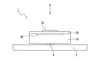
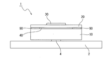
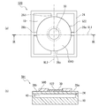
- the configuration of the first embodiment will be described with reference to FIGS. 1 to 5.
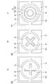
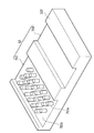
- the surface stress sensor 1 shown in FIGS. 1 to 5 is used, for example, as a sensor for detecting taste and smell, and includes the package substrate 2, the connection portion 4, the support base 10, and the detection base 20. Prepare.
- the package substrate 2 is formed of, for example, a metal, a polymer, a ceramic material, or the like, and is formed, for example, to a thickness on the order of millimeters.
- the connection portion 4 is disposed on one surface (upper surface in FIG. 1) of the package substrate 2 and is formed using, for example, an adhesive or solder. In the first embodiment, as an example, the case where the shape of the connection portion 4 is formed in a circular shape will be described.
- the support substrate 10 is disposed on one surface of the package substrate 2 and is attached to the package substrate 2 via the connection portion 4.
- the area of the support substrate 10 (in FIG. 1, the area of the support substrate 10 when the support substrate 10 is viewed in the vertical direction) is larger than the area of the connection portion 4.
- the thickness of the support base 10 (the length in the vertical direction of the support base 10 in FIG. 1) is set to 80 [ ⁇ m] or more.
- the thickness of the support substrate 10 may be set in the range of 80 ⁇ m to 750 ⁇ m.
- a material for forming the support substrate 10 for example, a material containing any one of silicon (Si: silicon), sapphire, gallium arsenide, glass, and quartz can be used.
- a BOX layer made of an oxide film or the like may be formed on the surface.
- the linear expansion coefficient of the support base 10 is 5.0 ⁇ 10 ⁇ 6 / ° C. or less.
- the linear expansion coefficient of the material which can be used as a material which forms the support base material 10 is described.
- the linear expansion coefficient of silicon is 3.9 ⁇ 10 ⁇ 6 / ° C. or less under an environment of normal temperature or more and 1000 ° C. or less.
- the linear expansion coefficient of sapphire is 9.0 ⁇ 10 ⁇ 6 / ° C. or less in an environment of 0 ° C. or more and 1000 ° C. or less.
- the linear expansion coefficient of gallium arsenide (GaAs) is 6.0 ⁇ 10 ⁇ 6 / ° C. or less under an environment of 0 K or more and 300 K or less.
- the linear expansion coefficient of glass float glass is 8.5 ⁇ 10 ⁇ 6 / ° C.
- the linear expansion coefficient of quartz is 0.59 ⁇ 10 ⁇ 6 / ° C. or less under an environment of 0 ° C. or more and 300 ° C. or less.
- the linear expansion coefficient of quartz has a peak in the vicinity of 300.degree.
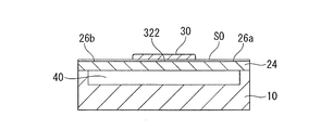
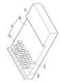
- the detection base 20 is laminated on one surface (upper surface in FIG. 1) of the support base 10, and the membrane 22, the frame member 24, and the connecting portion 26 are integrally formed. ing.
- the material which forms the detection base material 20 uses the material from which the difference of the linear expansion coefficient of the support base material 10 and the linear expansion coefficient of the detection base 20 becomes 1.2 * 10 ⁇ -5 > / degrees C or less .
- the case where the material forming the detection base 20 and the material forming the support base 10 are the same material will be described.
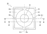
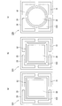
- the membrane 22 is formed in a plate shape. In the first embodiment, as an example, the case where the membrane 22 is formed in a disk shape will be described.
- the membrane 22 is an n-type semiconductor layer.
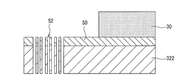
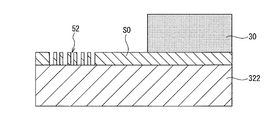
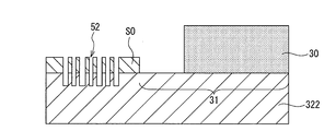
- a receptor 30 is formed by coating, for example.
- the receptor 30 (receptor) is formed, for example, using a solution of polyethylenimine (PEI) (which may be described as “PEI solution” in the following description), and is distorted by adsorption of gas molecules. Occurs. When molecules of the gas are adsorbed to the receptor 30 and distortion occurs in the receptor 30, surface stress is applied to the membrane 22, and the membrane 22 bends.
- PEI polyethylenimine
- membrane 22 deflects due to the applied surface stress as gas molecules adsorb to receptor 30.
- the configuration of the receptor 30 is not limited to a configuration in which distortion occurs when gas molecules are adsorbed, and for example, a configuration in which distortion occurs due to magnetism may be used. That is, the configuration of the receptor 30 may be appropriately changed in accordance with the detection target of the surface stress sensor 1.
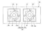
- the frame member 24 is formed in a cross-girder shape, and surrounds the membrane 22 with a gap as viewed from the thickness direction of the membrane 22.
- the viewpoint as viewed from the thickness direction of the membrane 22 is a viewpoint as viewed from above the surface stress sensor 1 (in FIG. 1, a viewpoint as viewed from the direction of the arrow II).
- the center of the frame member 24 overlaps the center of the membrane 22.
- the frame member 24 is connected to the surface (upper surface in FIG. 1) of the support base 10 opposite to the surface facing the package substrate 2 using various bonding techniques such as adhesion. ing.
- the outer peripheral surface of the support base 10 and the outer peripheral surface of the frame member 24 are flush with each other.
- the frame member 24 and the support base 10 are quadrilaterals of the same shape when viewed from the thickness direction of the membrane 22. This is realized, for example, by dicing the frame member 24 and the support base 10 after connecting the frame member 24 and the support base 10. That is, as viewed in the thickness direction of the membrane 22, the center of the frame member 24 overlaps the center of the support base 10.
- the support substrate 10 overlaps the membrane 22 and the frame member 24 when viewed in the thickness direction of the membrane 22.
- the connection portion 4 is disposed at a position overlapping at least a part of the membrane 22 when viewed in the thickness direction of the membrane 22. Further, when viewed in the thickness direction of the membrane 22, the area of the connection portion 4 is smaller than the area of the membrane 22.
- the package substrate 2 is connected to the surface (the lower surface in FIG. 1) opposite to the surface of the support base 10 facing the membrane 22.
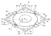
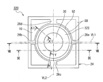
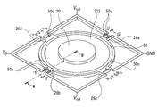
- connection portion 26 is formed in a band shape when viewed in the thickness direction of the membrane 22.
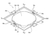
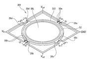
- the connecting portion 26 is disposed at a position overlapping the virtual straight lines VL1 and VL2 passing through the center of the membrane 22 when viewed in the thickness direction of the membrane 22, and connects the membrane 22 and the frame member 24. ing.
- the four connecting portions 26a to 26d are a pair of connecting portions 26a and 26b arranged at a position overlapping the straight line VL1 and a pair of connecting portions 26c arranged at a position overlapping the straight line VL2 orthogonal to the straight line VL1.
- a connecting portion 26d That is, the pair of connecting portions 26a and 26b, and the pair of connecting portions 26c and 26d are disposed at positions sandwiching the membrane 22 when viewed from the thickness direction of the membrane 22, and the membrane 22 and the frame member Concatenate 24
- a gap 40 is provided between the membrane 22 and the four connection portions 26 a to 26 d and the support base 10.
- the void 40 may be filled with the solution.
- the void portion 40 functions as a space that prevents the membrane 22 from sticking to the support base 10 when the membrane 22 bends to the side of the support base 10 during processing of the detection base 20.
- the four connectors 26a to 26d are provided with flexible resistors 50a to 50d, respectively.
- Each flexible resistor 50 changes its resistance value in accordance with the deflection occurring in the connection portion 26.
- the flexible resistor 50 is formed of a piezoresistor.
- the piezoresistor is formed, for example, by implanting ions into the connection portion 26, and has a resistance value that changes in accordance with the deflection occurring in the connection portion 26 as the membrane 22 flexes.
- the flexible resistor 50 is a p-type semiconductor layer.
- the four flexible resistors 50a to 50d are, for example, as shown in FIG.
- the flexible resistors 50 (connecting portion 26a and connecting portion 26c and connecting portion 26d, connecting portion 26b and connecting portion 26c and The connecting portion 26d) is connected.
- the four flexible resistors 50a-50d form a full Wheatstone bridge as shown in FIG.
- ⁇ is the resistivity of the piezoresistor
- l is the length of the piezoresistor
- w is the width of the piezoresistor
- t is the thickness of the piezoresistor
- ⁇ is induced in the piezoresistor Is the strain induced by piezoresistance, and .pi. Is the piezoresistance constant.
- x corresponds to the longitudinal direction of the cantilever
- y corresponds to the lateral direction of the cantilever
- z corresponds to the normal direction of the cantilever.
- the relationship between strain and stress can be derived from the generalized Hooke's law.
- the piezoresistor forming a p-type semiconductor layer is considered by being formed using single crystal Si (100). .
- the piezoresistance coefficient is determined by the relationships shown in the following equations (8) and (9).
- ⁇ 11, ⁇ 12 and ⁇ 44 are the basic piezoresistive coefficients of the crystal.
- ⁇ 11 is 10 ⁇ 11 Pa ⁇ 1 As +6.6.
- ⁇ 12 is -1.1 in 10-11 Pa-1 as a unit
- ⁇ 44 is +138.1 in 10-11 Pa-1 as a unit. Therefore, the piezoresistance coefficient ⁇ x is calculated to be 71.8 ⁇ 10 11 Pa ⁇ 1, and the piezoresistance coefficient ⁇ y is calculated to be ⁇ 66.3 ⁇ 10 11 Pa ⁇ 1.
- Equation (7) can be expressed by equation (10) below. It is possible to approximate to
- the piezoresistive signal (ie, ⁇ R / R) is primarily determined by the difference between ⁇ x and ⁇ y.
- the method of manufacturing the surface stress sensor 1 includes a laminate formation step, a first ion implantation step, a second ion implantation step, a heat treatment step, a wiring layer formation step, and a removal step.
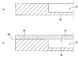
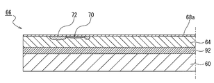
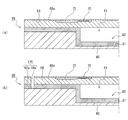
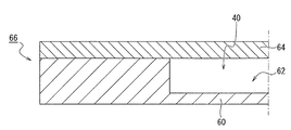
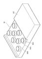
- a recess 62 (trench) is formed on one surface of the first silicon substrate 60 which is a material of the support base 10 using lithography and etching technology. Form. The depth of the recess 62 is set to, for example, 7 ⁇ m.
- a second silicon substrate 64 as a material of the detection base 20 is bonded to the first silicon substrate 60 in which the recess 62 is formed by using various bonding techniques such as adhesion, as shown in FIG.
- the stack 66 (Cavity wafer) is formed as shown in FIG.
- the void 40 surrounded by silicon (the first silicon substrate 60 and the second silicon substrate 64) is formed at the predetermined position of the laminated body 66. Be done.
- the recess 62 is formed on one surface of the support substrate 10, and the detection substrate 20 is bonded to the support substrate 10 so as to cover the recess 62.
- a laminated body 66 in which a gap 40 is provided between the sensor 10 and the detection base 20 is formed.
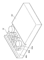
- first ion implantation process In the first ion implantation step, first, as shown in FIG. 7, the upper surface of the second silicon substrate 64 is oxidized to form a first silicon oxide film 68a, and a photoresist pattern (not shown) is formed. Using this, the first ion is selectively implanted into the flexible resistance region 70. As described above, in the first ion implantation step, one of the surfaces on the opposite side to the surface of the detection base 20 opposite to the support base 10 is selected outside the preset region including the center of the detection base 20. First ions are implanted into the area of the part (flexible resistance area 70).
- the photoresist used in the first ion implantation step is removed, and a pattern (not shown) of a photoresist different from that used in the first ion implantation step is formed.
- a second ion is implanted into the low resistance region 72.
- the second ions are implanted into a selected region outside the region (flexible resistance region 70) into which the first ions of the detection substrate 20 are implanted.
- heat treatment process In the heat treatment step, the photoresist used in the second ion implantation step is removed, and a heat treatment (annealing treatment) is performed on the stacked body 66 for the purpose of activating the first ion and the second ion. After heat treatment is performed on the stacked body 66, the first silicon oxide film 68a is removed. As described above, in the heat treatment step, the multilayer resistive element 66 into which the first ion and the second ion are implanted is heat treated to form the flexible resistance region 70 in the region into which the first ion is implanted. The low resistance region 72 is formed in the region into which the ions of.
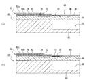
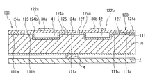
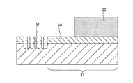
- the silicon nitride film 74 and the second silicon oxide film 68b are sequentially stacked on the upper surface of the second silicon substrate 64. Then, as shown in FIG. 8B, holes 76 are formed in the second silicon oxide film 68b by ordinary lithography and oxide film etching. Next, as shown in FIG. 9A, a laminated film 78 formed of Ti and TiN is formed on the second silicon oxide film 68b by sputtering, and heat treatment is performed.
- the laminated film 78 is a so-called barrier metal having a role of preventing abnormal diffusion of a metal film such as Al into Si, and the interface between Si and Ti existing at the bottom of the hole 76 is silicided by heat treatment. To form a low resistance connection. Further, as shown in FIG. 9B, a metal film 80 such as Al is laminated on the laminated film 78 by sputtering.
- the metal film 80 is patterned by photolithography and etching to form a wiring layer 82 as shown in FIG. Further, as shown in FIG. 10B, a third silicon oxide film 68c is stacked as an insulating layer.
- a photoresist which covers areas other than the membrane setting area 84 which is a predetermined area including the center of the flexible resistance area 70 and the detection base (area to be a membrane later). Form a pattern (not shown).
- the flexible resistance region 70 and the second silicon oxide film 68 b formed in the membrane setting region 84 are removed by the etching technique. Then, a photoresist pattern (not shown) which covers areas other than the membrane setting area 84 is formed, and as shown in FIG.
- the silicon nitride film 74 in the membrane setting area 84 is removed.
- a PAD 86 for obtaining an output from the flexible resistor 50 is formed by the usual photolithography and etching techniques.
- the wiring layer 82 electrically connected to the flexible resistor 50 is formed.
- the removal step a part of the membrane setting area 84 is cut away by etching to pattern two pairs of four connecting parts 26a to 26d. Therefore, in the removing step, the membrane 22 and the frame member are removed by removing the area other than the low resistance area 72 and the flexible resistance area 70 (area to be the connection portion 26 later) around the membrane setting area 84. 24, forming the connecting portion 26 and the flexible resistor 50.
- the receptor 30 is disposed in a gas atmosphere containing an odorous component, and the odorous component contained in the gas is adsorbed to the receptor 30.
- molecules of the gas are adsorbed to the receptor 30 and distortion occurs in the receptor 30, surface stress is applied to the membrane 22, and the membrane 22 bends.
- the frame member 24 is formed in a cross-girder shape and surrounds the membrane 22, and the connection part 26 connects the membrane 22 and the frame member 24 at both ends. Therefore, the end of the connection portion 26 connected to the membrane 22 is a free end, and the end connected to the frame member 24 is a fixed end.
- the connection portion 26 bends in response to the strain generated in the receiver 30. Then, the resistance value of the flexible resistor 50 changes in accordance with the bending occurring in the connecting portion 26, and a change in voltage corresponding to the change in the resistance value is output from the PAD 86 and used for data detection in a computer or the like.
- the surface stress sensor 1 there is a possibility that the package substrate 2 may be deformed (shrink, stretch, warp) due to a temperature change or the like generated in the use environment of the surface stress sensor 1, for example.
- the structure of the surface stress sensor 100 having the conventional structure that is, for example, as shown in FIG. 13A, in the structure in which the support base 10 is formed in a cylindrical shape and the membrane 22 floats in the hollow.
- the following problems occur. That is, in the surface stress sensor 100 having the conventional configuration, as shown in FIG. 13B, when the package substrate 2 is deformed (contracted), the support substrate 10 is also deformed along with the deformation of the package substrate 2. . Since the membrane 22 floats in the air and only a space exists between the membrane 22 and the package substrate 2, deformation of the support base 10 is permitted, and the membrane 22 is largely bent. Become. That is, the deformation of the package substrate 2 is applied to the membrane 22 as a stress. As a result, an offset is given to the output of the voltage or current by the flexible resistor 50, and the offset is changed according to the temperature change, so that the accuracy of the surface stress sensor 1 is deteriorated.
- the membrane 22 is largely deformed due to the change in stress received from the deformed package substrate 2, and the characteristics of the surface stress sensor 100 are changed. Therefore, the characteristics of the surface stress sensor 100 change during the inspection and mounting of the surface stress sensor 100, which makes inspection and calibration at the time of shipping the surface stress sensor 100 difficult.
- the support base 10 is present between the membrane 22 and the package substrate 2. Further, since the support base 10 is formed in a columnar shape, it has high rigidity as compared with the configuration in which the support base 10 is formed in a cylindrical shape as in the surface stress sensor 100 having the conventional configuration. doing. For this reason, in the case of the surface stress sensor 1 of the first embodiment, as shown in FIG. 14B, even if the package substrate 2 is deformed (contracted), the supporting base 10 has high rigidity. Because of this, the deformation of the support base 10 is suppressed, and the deflection of the membrane 22 is suppressed.
- the support base 10 since the support base 10 has high rigidity, it is insensitive to stress change of the package substrate 2 caused by temperature change etc., and stable sensing with high accuracy is possible. It becomes. Further, in the case of the surface stress sensor 1 of the first embodiment, the support base 10 is insensitive to stress change of the package substrate 2 caused by temperature change and the like, and the configuration of the package substrate 2 (strength, material, thickness, etc. Hard to be affected by For this reason, it becomes possible to use for package substrate 2 of various composition. Furthermore, in the case of the surface stress sensor 1 of the first embodiment, the center of the support base 10 overlaps the position where the connection portion 4 is disposed. In addition to this, the area of the support base 10 is larger than the area of the connection portion 4.
- the stress generated by the deformation of the package substrate 2 transmitted to the support substrate 10 through the connection portion 4 is reduced compared to the stress generated in the entire package substrate 2, and hence the support substrate The deformation of 10 is suppressed, and the deflection of the membrane 22 is suppressed. Therefore, with the configuration of the first embodiment, it is possible to reduce the stress applied to the membrane 22 by the deformation of the package substrate 2 and to suppress the deterioration of the measurement accuracy of the surface stress sensor 1.
- the technology of sensing information equivalent to human's five senses is compared with visual sense, auditory sense and tactile sense among the five senses. It becomes possible to apply to the sensor of the taste and the sense of smell which are not necessarily general.
- the above-described first embodiment is an example of the present invention, and the present invention is not limited to the above-described first embodiment, and the embodiment according to the present invention is applicable to any form other than this embodiment. Various modifications can be made according to the design and the like without departing from the technical concept.
- the support base 10 is configured to have high rigidity, and is insensitive to stress change of the package substrate 2 caused by temperature change or the like, and stable sensing with high accuracy becomes possible.
- the surface stress sensor 1 capable of suppressing the deterioration of the measurement accuracy by reducing the stress applied to the membrane 22 by the deformation of the package substrate 2.
- it is possible to improve the rigidity of the surface stress sensor 1 itself it is possible to prevent problems such as breakage during handling or the like that occur during handling.
- the flexible resistor 50 is a piezoresistor having a resistance value that changes in accordance with the deflection occurring in the connection portion 26 when the membrane 22 flexes. As a result, it becomes possible to detect the relative resistance change of the resistance value of the piezoresistor using the stress in the X direction and the Y direction induced by the piezoresistor, and the target molecule is adsorbed to the receptor 30 It is possible to determine whether or not.
- the membrane 22 and the frame member 24 are connected by four pairs of four connecting portions 26a to 26d, and the flexible resistor 50 is provided at each of the four connecting portions 26a to 26d.
- Two flexible resistors 50 form a full Wheatstone bridge. Since R1 and R3 have large deflection in the X direction, and R2 and R4 have large deflection in the Y direction, the relative resistance changes in R1 and R2 and R3 and R4 are reversed.
- the voltage of the output terminal Vout that divides the applied voltage VB by R1 and R2 changes by exhibiting the synergetic effect of R1 and R2 whose increase and decrease are opposite. The same is true for the splits in R3 and R4.
- the full Voutston bridge is advantageous in that both Vout voltages are reversed, so that both Vout voltages add as a result and all four piezoresistor changes contribute positively to increase sensitivity.
- the membrane 22 is an n-type semiconductor layer
- the flexible resistor 50 is a p-type semiconductor layer.
- the current flowing in the flexible resistor 50 does not flow in the membrane 22, and no noise is generated in the output voltage.
- a p-type semiconductor for the flexible resistor 50 it is possible to realize higher sensitivity than using n-type.
- the material forming the detection base 20 and the material forming the support base 10 are the same material. As a result, it becomes possible to reduce the difference between the amount of deformation of the detection base 20 and the amount of deformation of the support base 10 in response to the deformation of the package substrate 2 caused by temperature change etc. It is possible to
- the linear expansion coefficient of the support base 10 is 5.0 ⁇ 10 ⁇ 6 / ° C. or less. As a result, the rigidity of the support base 10 can be improved, and the amount of deformation of the detection base 20 with respect to the deformation of the package substrate 2 caused by a temperature change or the like can be reduced.
- the thickness of the support substrate 10 is 80 ⁇ m or more. As a result, the rigidity of the support base 10 can be improved, and the amount of deformation of the detection base 20 with respect to the deformation of the package substrate 2 caused by a temperature change or the like can be reduced.
- the support substrate 10 is formed of a material containing any of silicon, sapphire, gallium arsenide, glass, and quartz. As a result, it becomes easy to secure the conductivity required of the surface stress sensor 1.
- the semiconductor device further includes the package substrate 2 connected to the surface opposite to the surface facing the membrane 22 of the support substrate 10. As a result, mounting of the surface stress sensor 1 on various sensors becomes easy.
- the supporting base 10 and the package substrate 2 are connected by the connecting portion 4 disposed at a position overlapping at least a part of the membrane 22 when viewed in the thickness direction of the membrane 22. As a result, it is possible to connect the support base 10 and the package substrate 2 without using a bracket or the like, and it is possible to suppress the complication of the configuration.
- connection portion 4 is smaller than the area of the membrane 22 when viewed in the thickness direction of the membrane 22. For this reason, it is possible to reduce the stress generated by the deformation of the package substrate 2 transmitted to the support base 10 through the connection portion 4 more than the stress generated in the entire package substrate 2. As a result, it is possible to suppress the deformation of the support substrate 10 and to suppress the deflection of the membrane 22. Moreover, if it is a manufacturing method of the surface stress sensor of a first embodiment, it will become possible to produce an effect indicated below.
- a laminate formation step, a first ion implantation step, a second ion implantation step, a heat treatment step, a wiring layer formation step, and a removal step are provided.
- the concave portion 62 is formed on one surface of the support base 10
- the detection base 20 is attached to the support base 10 so as to cover the concave portion 62, thereby detecting the support base 10 and the detection base 20.
- a laminate 66 in which the air gap 40 is provided between the substrate 20 is formed.
- the first ion implantation step of the surface opposite to the surface facing the support substrate 10 of the detection substrate 20, a selected partial region outside the preset region including the center of the detection substrate 20 , Inject the first ion.
- second ions are implanted into a selected region outside the region of the detection substrate 20 where the first ions are implanted.
- the laminate 66 in which the first ion and the second ion are implanted is heat treated to form the flexible resistance region 70 in the region where the first ion is implanted, and the second ion.
- a low resistance region 72 is formed in the implanted region.
- the wiring layer formation step the wiring layer 82 electrically connected to the flexible resistor 50 is formed.
- the membrane 22, the frame member 24, and the connecting portion are removed by removing a region other than the low resistance region 72 and the flexible resistance region 70 around a preset region including the center of the detection substrate 20. 26 and form a flexible resistor 50.
- the support base 10 is configured to have high rigidity, and is insensitive to stress change of the package substrate 2 caused by temperature change or the like, and stable sensing with high accuracy becomes possible.
- a method of manufacturing a surface stress sensor capable of reducing the stress applied to the membrane 22 by the deformation of the package substrate 2 and suppressing the deterioration of the measurement accuracy.
- it is possible to improve the rigidity of the surface stress sensor 1 itself it is possible to prevent problems such as breakage during handling or the like that occur during handling.
- the concave portion 62 is formed on one surface of the first silicon substrate 60 which is a material of the support base 10, whereby the air gap 40 is formed between the membrane 22 and the support base 10.
- a void is formed between the membrane 22 and the support base 10 by forming a recess on the surface of the second silicon substrate 64, which is the material of the detection base 20, facing the support base 10. It is also good.
- the flexible resistors 50a to 50d are respectively provided in the two pairs of four connecting parts 26a to 26d, but the present invention is not limited to this. That is, the flexible resistors 50 may be provided in each of the two connecting portions 26 which are a pair.
- the flexible resistor 50 is provided in all the four connecting portions 26a to 26d. However, the present invention is not limited to this.
- the flexible resistor 50 may be provided.
- the area of the connection portion 4 is smaller than the area of the membrane 22 when viewed from the thickness direction of the membrane 22. However, the present invention is not limited to this. The area may be equal to or larger than the area of the membrane 22.
- the shape of the connection portion 4 is circular, but it is not limited to this. For example, the shape of the connection portion 4 may be square. Also, a plurality of connection portions 4 may be formed.
- the material for forming the detection base 20 and the material for forming the support base 10 are the same material, but the present invention is not limited to this.
- the material to be formed and the material to form the support substrate 10 may be different materials.
- the detection base according to the deformation of the package substrate 2 It is possible to reduce the difference between the amount of deformation of the material 20 and the amount of deformation of the support substrate 10. This makes it possible to suppress the deflection of the membrane 22.
- the linear expansion coefficient of the support base 10 is 5.0 ⁇ 10 ⁇ 6 / ° C. or less
- the present invention is not limited to this, and the linear expansion coefficient of the support base 10 is Or less than 1.0 ⁇ 10 ⁇ 5 / ° C. Even in this case, the rigidity of the support base 10 can be improved, and the amount of deformation of the detection base 20 with respect to the deformation of the package substrate 2 caused by a temperature change or the like can be reduced.
- the frame member 24 has a surface on the opposite side to the surface of the support base 10 facing the package substrate 2 via the connection layer 90 (in FIG. It is the same as the first embodiment described above except that it is connected to the upper surface).
- the connection layer 90 is formed using silicon dioxide (SiO 2 ) or the like.
- SiO 2 silicon dioxide
- the method of manufacturing the surface stress sensor 1 includes a laminate forming step, a first ion implantation step, a second ion implantation step, a heat treatment step, a hole forming step, a void forming step, a hole sealing step, A wiring layer forming step and a removing step are provided.
- a sacrificial layer 92 formed using a silicon oxide film is laminated on a first silicon substrate 60 which is a material of the support base 10. Furthermore, a second silicon substrate 64 which is a material of the detection base 20 is stacked on the sacrificial layer 92.
- a silicon nitride film or a metal film such as aluminum, titanium, copper, tungsten or the like may be used.
- the sacrificial layer 92 is laminated on the support substrate 10, and the detection substrate 20 is further laminated on the sacrificial layer 92 to form a laminate 66.
- first ion implantation process In the first ion implantation step, first, as shown in FIG. 16, the second silicon substrate 64 is oxidized to oxidize the upper surface of the second silicon substrate 64 to form a first silicon oxide film 68a. . Next, a photoresist pattern (not shown) is formed on the second silicon substrate 64 on which the first silicon oxide film 68 a is formed, and Implant ions. As described above, in the first ion implantation step, one of the surfaces on the opposite side to the surface of the detection base 20 opposite to the support base 10 is selected outside the preset region including the center of the detection base 20. First ions are implanted into the area of the part (flexible resistance area 70).
- the photoresist used in the first ion implantation step is removed, and a pattern (not shown) of a photoresist different from that used in the first ion implantation step is formed to reduce the resistance Region 72 is implanted with a second ion.
- the second ions are implanted into a selected region outside the region (flexible resistance region 70) into which the first ions of the detection substrate 20 are implanted.
- heat treatment process In the heat treatment step, the photoresist used in the second ion implantation step is removed, and a heat treatment (annealing treatment) is performed on the stacked body 66 for the purpose of activating the first ion and the second ion. After heat treatment is performed on the stacked body 66, the first silicon oxide film 68a is removed. As described above, in the heat treatment step, the multilayer resistive element 66 into which the first ion and the second ion are implanted is heat treated to form the flexible resistance region 70 in the region into which the first ion is implanted. The low resistance region 72 is formed in the region into which the ions of.
- a pattern of holes (not shown) is formed on the upper surface of the second silicon substrate 64 by a general photolithographic technique.
- dry etching is performed using the pattern of holes as a mask to form holes 76 in the second silicon substrate 64 as shown in FIG.
- the diameter of the hole 76 is set to, for example, 0.28 [ ⁇ m] and to a depth reaching the sacrificial layer 92.
- the hole 76 penetrating to the sacrificial layer 92 is formed in the area adjacent to the area in which the flexible resistance area 70 and the low resistance area 72 are formed of the detection base 20.
- void part formation process In the void formation step, only the sacrificial layer 92 is selectively etched by permeating HFVap through the holes 76 to the side of the first silicon substrate 60, as shown in FIG. An air gap 40 is formed between the two silicon substrate 64.
- HF wet etching is not used is to avoid the occurrence of a defect (also referred to as stiction) in which the void 40 is crushed by surface tension of pure water or the like during drying after the void 40 is formed. It is for.
- the sacrificial layer 92 disposed between the flexible resistance region 70 and the support base 10 is removed by etching through the holes 76, and the support base 10 and the detection base are removed.
- An air gap 40 is provided between the material 20 and the material 20.
- the holes 76 are sealed by the oxide film 94.
- a method of sealing the hole 76 for example, it is effective to combine thermal oxidation treatment and CVD, but if the diameter of the hole 76 is small, it is also possible to use only the CVD.
- the hole 76 is sealed by forming the oxide film 94 on the surface opposite to the surface of the detection substrate 20 facing the support substrate 10.
- the wiring layer forming process is performed in the same procedure as the first embodiment described above, and thus the description thereof is omitted.
- the wiring layer 82 electrically connected to the flexible resistor 50 is formed.
- the removal process is performed in the same procedure as the first embodiment described above, and thus the description thereof is omitted. Therefore, in the removing step, the membrane 22, the frame member 24, and the like are removed by removing the area other than the low resistance area 72 and the flexible resistance area 70 around the preset area including the center of the detection substrate 20.
- the connection 26 forms a flexible resistor 50.
- Laminate formation process first ion implantation process, second ion implantation process, heat treatment process, hole formation process, void formation process, hole sealing process, wiring layer formation process, A removal process is provided.
- the laminate formation step the sacrificial layer 92 is laminated on the support substrate 10, and the detection substrate 20 is further laminated on the sacrificial layer 92 to form a laminate 66.
- the first ion implantation step of the surface opposite to the surface facing the support substrate 10 of the detection substrate 20, a selected partial region outside the preset region including the center of the detection substrate 20 , Inject the first ion.
- second ions are implanted into a selected region outside the region of the detection substrate 20 where the first ions are implanted.
- the laminate 66 in which the first ion and the second ion are implanted is heat treated to form the flexible resistance region 70 in the region where the first ion is implanted, and the second ion.
- a low resistance region 72 is formed in the implanted region.
- holes 76 penetrating to the sacrificial layer 92 are formed in the area adjacent to the area in which the flexible resistance area 70 and the low resistance area 72 are formed of the detection substrate 20.
- the sacrificial layer 92 disposed between the flexible resistance region 70 and the support base 10 is removed by etching through the holes 76, and the support base 10 and the detection base 20 are removed. A gap 40 is provided between the two.
- an oxide film 94 is formed on the surface of the detection base 20 opposite to the surface facing the support base 10 to seal the holes 76.
- the wiring layer formation step the wiring layer 82 electrically connected to the flexible resistor 50 is formed.
- the membrane 22 and the frame member 24 are removed by removing an area other than the low resistance area 72 and the flexible resistance area 70 around the preset membrane setting area 84 including the center of the detection substrate 20. , The connecting portion 26 and the flexible resistor 50.
- the support base 10 is configured to have high rigidity, and is insensitive to stress change of the package substrate 2 caused by temperature change or the like, and stable sensing with high accuracy becomes possible.
- a method of manufacturing a surface stress sensor capable of reducing the stress applied to the membrane 22 by the deformation of the package substrate 2 and suppressing the deterioration of the measurement accuracy.
- it is possible to improve the rigidity of the surface stress sensor 1 itself it is possible to prevent problems such as breakage during handling or the like that occur during handling.
- a BOX (Buried Oxide) layer may be provided on the surface of the support base 10 for the purpose of insulation between the support base 10 and the detection base 20.
- the BOX layer is formed, for example, by thermally oxidizing a Si substrate. Since the thermal oxidation of Si induces stress in the Si crystal, the BOX layer may cause the membrane of the surface stress sensor to bend. The deflection of the membrane due to the stress of the BOX layer is offset in the surface stress sensor, and the improvement of the detection accuracy of the surface stress sensor is suppressed.
- the surface stress sensor which concerns on 3rd embodiment of this invention can suppress the fall of the measurement precision of the surface stress sensor resulting from a BOX layer in the structure which provided the BOX layer in the surface of a support base material.
- FIG. 20 is a cross-sectional view showing a cross section of the surface stress sensor 101 according to the third embodiment.
- FIG. 21 is a plan view of the surface stress sensor 101 shown in FIG. In FIGS. 20 and 21, the wiring layers formed on the top surface of the surface stress sensor 101 are not shown.
- the surface stress sensor 101 is provided with the connection layer 111 which is a BOX layer on the surface of the support base 10, and the surface stress sensor 101 is plural on one support base 10.
- the surface stress sensor 101 is configured to be able to detect different types of gas by forming the receptor 30a and the receptor 30b with different materials.
- the receptor 30a and the receptor 30b may be formed of the same material.
- the membranes 122a and 122b correspond to the membrane 22 of the first embodiment
- the receptors 30a and 30b correspond to the receptor 30 of the first embodiment
- the gaps 41 and 42 correspond to the gaps 40 of the first embodiment. In order to correspond to, the explanation is omitted.
- connection layer 111 In the surface stress sensor 101, the connection layer 111 is provided on the surface of the support base 10 facing the detection base 120, and a part of the connection layer 111 is removed to form the groove portions 125 and 127. On the surface of the surface of the support base 10 opposite to the detection base 120, two trenches to be the void 40 (41, 42) are formed.
- the connection layer 111 (111a, 111b, 111c) is formed on the surface of the support base 10 after the trench formation facing the detection base 120 so as to cover the surface of the support base 10 and the surface of the trench.
- the connection layers 111a, 111b, and 111c will be described later.
- the connection layer 111 may be provided on the surface of the surface of the support base 10 facing the package substrate 2 (the lower surface in FIG. 20).
- the grooves 125 and 127 are provided at positions surrounding the rectangular gaps 41 and 42 in a plan view, and penetrate the frame member 124 and the connection layer 111 of the detection base 120. It is formed.
- the grooves 125 and 127 are formed by removing a part of each of the frame member 124 and the connection layer 111.
- the grooves 125 and 127 have an annular shape corresponding to the outer shape of the gaps 41 and 42 in a plan view, and for example, are formed in a rectangular ring shape having a rectangular outer shape in a plan view.
- the grooves 125 and 127 are provided, for example, in the outer regions of the flexible resistors 50a to 50d around the gaps 41 and 42 in plan view.
- connection layer 111 is separated by groove 125 into connection layer 111 b located inside groove 125 (the area on membrane 122 a formation side) in plan view and connection layer 111 a located outside groove 125.
- Ru The connection layer 111 is separated by the groove portion 127 into a connection layer 111 c located inside the groove portion 127 (area on the membrane 122 b formation side) in plan view and a connection layer 111 a located outside the groove portion 125.
- the frame member 124 is separated by the groove portion 125 into a frame member 124 b located inside the groove portion 125 in plan view and a frame member 124 a located outside the groove portion 125.
- connection layers 111a, 111b, and 111c are hereinafter referred to as connection layers 111 when the connection layers 111a, 111b, and 111c are not distinguished from one another. Moreover, when not distinguishing frame members 124a, 124b and 124c, it describes as the frame member 124.
- FIG. 1 when not distinguishing frame members 124a, 124b and 124c, it describes as the frame member 124.
- the frame member 124 b located inside the groove portion 125 is connected to the membrane 122 a by four (two pairs) of connection portions 26. Further, the frame member 124 c located inside the groove portion 127 is connected to the membrane 122 b by the four (two pairs) connection portions 26.
- connection layer 111b and the frame member 124b located inside the groove 125 are separated from the connection layer 111a and the frame member 124a located outside the groove 125 where the area is large and stress is easily generated. There is. Therefore, even when a stress is generated in the connection layer 111a, the stress can be released to the groove portion 125, and the influence of the stress generated in the connection layer 111a on the membrane 122a can be reduced.
- connection layer 111c and the frame member 124c located inside the groove 127 are separated from the connection layer 111a and the frame member 124a located outside the groove 127 where the area is large and stress is easily generated. . Therefore, even when a stress is generated in the connection layer 111a, the stress can be released to the groove portion 127, and the influence of the stress generated in the connection layer 111a on the membrane 122b can be reduced.
- the grooves 125 and 127 are provided at positions closer to the membranes 122a and 122b.
- the area of the connection layers 111b and 111c can be further reduced, and the stress that the membranes 122a and 122b receive from the connection layers 111b and 111c can be further reduced. Therefore, by providing the groove portions 125 and 127, stress applied to the membranes 122a and 122b is reduced as compared with the case where the groove portions 125 and 127 are not provided, and the offset of the surface stress sensor 101 can be reduced.
- the grooves 125 and 127 may be provided in an area several tens ⁇ m (for example, 40 ⁇ m) or more outside the outer periphery of the gaps 41 and 42. preferable.
- the groove 125 is formed so that the distances L1 to L4 between the groove 125 and the outer periphery of the air gap 41 are equal at any position between the groove 125 and the outer periphery of the air gap 41. More preferably, it is formed. That is, it is more preferable that the groove portion 125 be formed such that all of the distances L1, L2, L3 and L4 shown in FIG. 21 become equal. Further, it is more preferable that the distances L1 ′ to L4 ′ between the groove 127 and the outer periphery of the air gap 42 be equal at any position between the groove 127 and the outer periphery of the air gap 42. .
- the groove portion 127 be formed such that all the distances L1 ′, L2 ′, L3 ′, and L4 ′ shown in FIG. 21 become equal.
- Adjacent grooves may have a part of the grooves formed in common. That is, in FIG. 21, the groove located on the right side of the groove portion 125 formed adjacent to each other and the groove located on the left side of the groove portion 127 may be integrally formed. With this configuration, the groove portion 125 and the groove portion 127 are formed in close contact with each other, whereby the membranes 122a and 122b can be disposed closer to each other, and the surface stress sensor 101 can be miniaturized.
- the planar shape of the gaps 41 and 42 is not limited to a rectangle, and may be a circle or a polygon.
- the grooves 125 and 127 preferably have shapes corresponding to the planar shapes of the gaps 41 and 42, respectively.
- connection layer 111a and the frame member 124a located outside the grooves 125 and 127 may be removed. This configuration is preferable because stress is not applied to the membranes 122a and 122b from the outside of the grooves 125 and 127. Furthermore, the connection layer 111a and the connection layers 111b and 111c may not be completely separated from each other as long as the stress from the connection layer 111a to the connection layers 111b and 111c is small. For example, a connecting portion (not shown) connecting the connection layer 111a and the connection layer 111b may be thinly formed on the bottom surface of the groove portion 125 (the surface of the support base 10).
- the method of manufacturing the surface stress sensor 101 includes a laminate formation step, a first ion implantation step, a second ion implantation step, a heat treatment step, a groove formation step, a wiring layer formation step, and a removal step.
- a plurality of concave portions 62 are formed on one surface of the first silicon substrate 60 which is a material of the support base 10 using lithography and etching techniques. Form).
- FIG. 22 (a) only the recess 62 which will be the void 41 later is shown.
- thermal oxidation is performed on the first silicon substrate 60 in which the plurality of recesses 62 are formed to form a thermal oxide film 61 on at least the surface of the first silicon substrate 60 on which the recesses 62 are formed.
- the second silicon substrate 64 as the material of the detection base 20 is bonded to the first silicon substrate 60 having the thermal oxide film 61 formed on the surface on which the recess 62 is formed. Bonding using various bonding techniques. At this time, the second silicon substrate 64 is disposed so as to cover the plurality of recesses 62 and is bonded to the first silicon substrate 60. Thereby, a stacked body 66 (Cavity wafer) is formed.
- the top, bottom, left, and right portions of the stack 66 are surrounded by the thermal oxide film 61 formed on the second silicon substrate 64 and the first silicon substrate 60.
- the void 41 is formed.
- gap part 42 which is not shown in figure is simultaneously formed.
- the plurality of concave portions 62 to be the void portions 41 and 42 are formed in one surface of the first silicon substrate 60 to be the supporting base material 10.
- a thermal oxide film 61 is formed on at least one surface.
- the second silicon substrate 64 to be the detection base 120 is attached to the support base 10 so as to cover the plurality of concave portions 62.
- the air gaps 41, 42 are provided between the first silicon substrate 60 and the second silicon substrate 64, and heat is generated between the support base 10 and the detection base 120 at the outer periphery of the air gaps 41, 42.
- a stacked body 66 provided with the oxide film 61 is formed.
- the entire first silicon substrate 60 may be thermally oxidized to form a thermal oxide film 61 on the entire surface, back surface and side surfaces (upper surface, lower surface and left surface in FIG. 22) of the first silicon substrate 60.
- the surface stress sensor 101 in which the connection layers 111 are formed on both surfaces (upper and lower surfaces in FIG. 20) of the support base 10 can be obtained by singulating with a dicing blade at the end of the manufacturing process. .
- the first ion implantation step is performed in the same procedure as the above-described first embodiment, and thus the description thereof is omitted. As described above, in the first ion implantation step, one of the surfaces on the opposite side to the surface facing the support substrate 10 of the detection substrate 120 is selected outside the preset region including the center of the detection substrate 120 First ions are implanted into the area of the part (flexible resistance area 70).
- the second ion implantation step is performed in the same procedure as the first embodiment described above, and thus the description thereof is omitted.
- the second ions are implanted into a selected region outside the region (flexible resistance region 70) into which the first ions of the detection substrate 120 are implanted (FIG. (A).
- Heat treatment process The heat treatment process is performed in the same procedure as the first embodiment described above, and thus the description thereof is omitted.
- the multilayer resistive element 66 into which the first ion and the second ion are implanted is heat treated to form the flexible resistance region 70 in the region into which the first ion is implanted.
- the low resistance region 72 is formed in the region where the ions of the above are implanted (FIG. 23A).
- the second silicon substrate 64 is penetrated in the outer region of the region in which the flexible resistance region 70 and the low resistance region 72 of the laminated body 66 after heat treatment are formed.
- a groove 64 a having the thermal oxide film 61 as a bottom surface is formed.
- the grooves 64a are formed by dry etching using a photoresist pattern (not shown) as a mask.
- the groove 64a is formed, for example, in a shape along the shape of the void portions 41 and 42 at a position surrounding each of the void portions 41 and 42 having a rectangular shape in plan view.
- the groove portion 125 is formed by the groove 64a and the groove 61a.
- the groove 127 is similarly formed.
- the thermally oxidized film 61 to be the substrate 64 and the connection layer 111 is removed to form the groove portions 125 and 127 (FIG. 23A).
- the wiring layer forming process is performed in the same procedure as the first embodiment described above, and thus the description thereof is omitted.
- the wiring layer 82 electrically connected to the flexible resistor 50 is formed.
- the removal process is performed in the same procedure as the first embodiment described above, and thus the description thereof is omitted. Therefore, in the removing step, the membranes 122a and 122b, and the frame member are removed by removing the regions other than the low resistance region 72 and the flexible resistance region 70 around the preset region including the center of the detection base 120 124 (124a, 124b), connecting portion 26, forming a flexible resistance.
- the operation and action of the third embodiment are the same as those of the first and second embodiments described above in addition to the connection layer 111 a located outside the grooves 125 and 127 by the grooves 125 and 127.
- the resulting stress can be prevented from being transmitted to the membranes 122a and 122b.
- the above-described third embodiment is an example of the present invention, and the present invention is not limited to the above-described third embodiment, and the embodiment according to the present invention is a form other than this embodiment. Various modifications can be made according to the design and the like without departing from the technical concept.
- the distance between the grooves 125 and 127 and the outer periphery of the gaps 41 and 42 is equal to each other at any position of the grooves 125 and the gaps 41 and the grooves 127 and the gaps 42. preferable.
- the stress applied from the periphery of the membrane 122a and the stress applied from the periphery of the membrane 122b can be substantially equalized, and the offset of the surface stress sensor 101 can be isotropically reduced.
- a part of the grooves 125 and 127 may be formed in common (integrally). With this configuration, the membranes 122a and 122b can be disposed closer to each other, and the surface stress sensor 101 can be miniaturized.
- the recess 62 is formed on one surface of the support base 10, and the thermal oxide film 61 is formed on the surface of the support base 10 on which the recess 62 is formed, and then the recess 62 is formed on the support base 10.
- the gap 40 is provided between the support base 10 and the detection base 120, and the support base 10 and the detection base are provided on the outer periphery of the gaps 41 and 42.
- the laminate 66 in which the first ion and the second ion are implanted is heat treated to form the flexible resistance region 70 in the region where the first ion is implanted, and the second ion.
- a low resistance region 72 is formed in the implanted region.
- the detection base 120 and the thermal oxide film 61 are formed in the area outside the flexible resistance area 70 forming the flexible resistances 50 a to 50 d of the detection base 120 and the low resistance area 72. Are removed to form grooves 125 and 127.
- the wiring layer forming step a wiring layer electrically connected to the flexible resistor is formed.
- the membranes 122a and 122b and the frame member 124 are removed by removing areas other than the low resistance area 72 and the flexible resistance area 70 around a predetermined area including the center of the detection base 120 and excluding the low resistance area 72 and the flexible resistance area 70.
- 124a, 124b, 124c) the connection 26 and the flexible resistor 50 are formed.
- the influence on the membranes 122a and 122b of the stress generated in the connection layer 111 is reduced in a simple step, and the stability is high. Sensing is possible.
- the surface stress sensor 101 according to the fourth embodiment has a structure in which a plurality of sensor units are provided as in the third embodiment, and a groove is provided on the outer periphery of the sensor unit. Similarly, the connection layer 90 is provided on the support substrate 10.
- the other configuration is the same as that of the second embodiment described above, so the description will be omitted.
- the method of manufacturing the surface stress sensor 101 includes a laminate formation step, a first ion implantation step, a second ion implantation step, a heat treatment step, a hole formation step, a void formation step, a hole sealing step A wiring layer forming step and a removing step are provided.
- laminate formation process In the laminated body forming step, since the laminated body 66 is formed in the same procedure (FIG. 16) as the second embodiment described above, the description thereof is omitted. As described above, in the laminate formation step, the sacrificial layer 92 is laminated on the support substrate 10, and the detection substrate 120 is further laminated on the sacrificial layer 92 to form a laminate 66.
- first ion implantation process In the first ion implantation step, since the first ions are implanted in the same procedure (FIG. 16) as the second embodiment described above, the description thereof is omitted. As described above, in the first ion implantation step, one of the surfaces on the opposite side to the surface facing the support substrate 10 of the detection substrate 120 is selected outside the preset region including the center of the detection substrate 120 First ions are implanted into the area of the part (flexible resistance area 70).
- the second ions are implanted in the same procedure (FIG. 16) as the second embodiment described above, the description thereof is omitted.
- the second ions are implanted into a selected region outside the region (flexible resistance region 70) into which the first ions of the detection substrate 120 are implanted.
- the heat treatment step since the heat treatment is performed in the same procedure (FIG. 16) as the second embodiment described above, the description thereof is omitted.
- the multilayer resistive element 66 into which the first ion and the second ion are implanted is heat treated to form the flexible resistance region 70 in the region into which the first ion is implanted.
- the low resistance region 72 is formed in the region into which the ions of.
- a pattern of holes and trenches (not shown) is formed on the upper surface of the second silicon substrate 64 by a general photolithographic technique.
- a pattern of holes is formed in a region corresponding to the void formation region of the second silicon substrate 64.
- a region corresponding to the void formation region of the second silicon substrate 64 is a region adjacent to the region in which the flexible resistance region 70 and the low resistance region 72 of the detection base 120 are formed.
- the pattern of the grooves is formed in the region outside the void formation region of the second silicon substrate 64.
- the area outside the void forming area of the second silicon substrate 64 is the area outside the area in which the flexible resistance area 70 and the low resistance area 72 of the detection substrate 120 are formed.
- the holes 76 are formed in a region corresponding to the void formation region of the second silicon substrate 64.
- the groove 77 is formed in a region outside the void forming region of the second silicon substrate 64 so as to surround the void forming region.
- the diameter of the hole 76 and the width of the groove 77 are set to, for example, 0.28 ⁇ m and to a depth reaching the sacrificial layer 92.
- the hole forming step the area adjacent to the area where the flexible resistance area 70 and the low resistance area 72 are formed in the detection base 120, and the area where the flexible resistance area 70 and the low resistance area 72 are formed. In the outer region, holes 76 and trenches 77 penetrating to the sacrificial layer 92 are formed.
- void part formation process In the void formation step, only the sacrificial layer 92 is selectively etched by permeating HFVap through the holes 76 and the grooves 77 to the side of the first silicon substrate 60, as shown in FIG. An air gap 40 and a groove 93 are formed between 60 and the second silicon substrate 64. As described above, in the void formation step, a part of the sacrificial layer 92 disposed between the flexible resistance region 70 and the support base 10 is removed by etching through the holes 76, thereby the support base 10. A gap 40 is provided between the and the detection substrate 20.
- the sacrificial layer 92 in the region outside the region in which the flexible resistance region 70 and the low resistance region 72 are formed is removed by etching through the groove 77 to form the groove 77 and the groove 93.
- the groove portion 125 is formed by this.
- the groove part 127 shown in FIG. 20 is formed using the groove
- the hole sealing step since the holes 76 are sealed in the same procedure as the above-described second embodiment, the description thereof is omitted.
- the hole sealing step as shown in FIG. 26, the hole 76 and the groove 77 are sealed by the oxide film 94.
- the oxide film 94 is formed on the surface of the detection base 20 opposite to the surface facing the support base 10 to seal the hole 76 and the groove 77.
- the wiring layer forming process is performed in the same procedure as the first embodiment described above, and thus the description thereof is omitted.
- the wiring layer electrically connected to the flexible resistor is formed.
- the removal process is performed in the same procedure as the first embodiment described above, and thus the description thereof is omitted. Therefore, in the removing step, the membranes 122a and 122b and the frame member are removed by removing the regions other than the low resistance region 72 and the flexible resistance region 70 around the preset region including the center of the detection substrate 20. 124 (124a, 124b), connecting portion 26, forming a flexible resistance.
- Laminate formation process first ion implantation process, second ion implantation process, heat treatment process, hole formation process, void formation process, groove formation process, hole sealing process, wiring
- a layer forming process and a removing process are provided.
- the sacrificial layer 92 is laminated on the support substrate 10, and the detection substrate 120 is further laminated on the sacrificial layer 92 to form a laminate 66.
- the first ion implantation step of the surface on the opposite side to the surface facing the support substrate 10 of the detection substrate 120, a selected partial region outside the preset region including the center of the detection substrate 120 , Inject the first ion.
- second ions are implanted into a selected region outside the region of the detection substrate 120 where the first ions are implanted.
- the laminate 66 in which the first ion and the second ion are implanted is heat treated to form the flexible resistance region 70 in the region where the first ion is implanted, and the second ion.
- a low resistance region 72 is formed in the implanted region.
- holes 76 penetrating to the sacrificial layer 92 are formed in the area adjacent to the area in which the flexible resistance area 70 and the low resistance area 72 are formed of the detection substrate 120. Further, in the hole forming step, a groove 77 penetrating to the sacrificial layer 92 and surrounding the previously set region in plan view is formed in the region outside the region where the flexible resistance region 70 and the low resistance region 72 are formed. .
- the sacrificial layer 92 disposed between the flexible resistance region 70 and the support base 10 is removed by etching through the holes 76, and the support base 10 and the detection base 120 are removed. A gap 40 is provided between the two.
- the sacrificial layer 92 exposed from the groove 77 is removed by etching through the groove 77 to form a groove penetrating the detection base 120 (second silicon substrate 64) and the sacrificial layer 92.
- an oxide film 94 is formed on the surface of the detection base 120 opposite to the surface facing the support base 10 to seal the holes 76 and the grooves 77.
- the wiring layer formation step the wiring layer 82 electrically connected to the flexible resistor 50 is formed.
- the membranes 122a and 122b, and the frame are removed by removing the area around the preset membrane setting area 84 including the center of the detection base 120 and excluding the low resistance area 72 and the flexible resistance area 70.
- the members 124 (124 a, 124 b), the connecting portion 26 and the flexible resistor 50 are formed.
- the influence of the stress generated in the connection layer 111 on the membranes 122a and 122b in a simple process is reduced, and the stability is high with high accuracy. Sensing is possible.
- the surface stress sensor 1 of the embodiment has the same configuration as that described in the first embodiment, that is, the support base is formed in a columnar shape, and the support base 10 is between the membrane 22 and the package substrate 2. It has an existing configuration (see FIG. 14).
- the support base material is formed in a tubular shape, and the membrane has a hollow structure (see FIG. 13).
- the performance is evaluated by simulation by detecting the change of the output in the situation where the package substrate is elongated by the temperature rise (10 ° C.) I made an evaluation.
- evaluation results As a result of detecting the change of the output in the situation where the package substrate has expanded, in the example, the degree of change of the output is about 1/3 compared to the comparative example.
- the surface stress sensor 1 of the embodiment can reduce the stress applied to the membrane by the deformation of the package substrate to about 1/3 as compared with the surface stress sensor of the comparative example. confirmed.
- the invention according to the fifth embodiment is, for example, a semiconductor device having a MEMS structure having a movable portion, and the surface stress sensor in which the movable portion is formed by releasing the pressure of the gap formed in the base material;
- the present invention relates to a method of manufacturing a sensor.
- the film thickness of the film base may be thin at the time of etching and there is a risk of breakage.
- membrane base material is a base material which forms the layer arrange
- membrane base material is disclosed by providing a notch in a film
- it is difficult to suppress the breakage of the membrane base when the technique of providing the notch in the membrane base is applied to a method of patterning the membrane base by one etching to form the movable part.
- a surface stress sensor capable of suppressing breakage of a film substrate generated during processing accompanied by pressure release and a method of manufacturing the surface stress sensor will be described.
- the surface stress sensor 201 shown in FIGS. 27 to 30 is, for example, an element used for a surface stress sensor that detects taste or smell of gas or liquid. Further, the surface stress sensor 201 includes the package substrate 2, the connection portion 4 and the support base 10 as in the surface stress sensor 1 of the first embodiment, but instead of the detection base 20, a film base is used. It differs from the surface stress sensor 1 of the first embodiment in that the material 220 is provided. Hereinafter, the membrane substrate 220 will be described in detail. The description of the package substrate 2, the connection portion 4 and the support base 10 will be omitted.
- the membrane substrate 220 is laminated on one surface (upper surface in FIG. 28) of the support substrate 10, and the membrane 22, the frame member 24, the connecting portion 26, and the peripheral film portion 28 are integrated. And is formed.
- a receptor 30 is provided on one side of the membrane 22.
- the membrane 22, the frame member 24 and the connecting portion 26, and the receiver 30 have the same configuration as the membrane 22, the frame member 24 and the connecting portion 26, and the receiver 30 in the detection base 20 of the first embodiment Description is omitted because there is.
- the configuration provided with the membrane base 220 described in the fifth embodiment can also be applied to a configuration in which the receptor 30 is not provided on the membrane 22. That is, the configuration described in the fifth embodiment is also applied to a hollow structural element other than a surface stress sensor, which is a device of a MEMS structure having a film base disposed above a cavity forming a void. be able to.
- membrane base 220 uses the material from which the difference of the linear expansion coefficient of the support base 10 and the linear expansion coefficient of the film
- the peripheral film unit 28 will be described in detail.
- the peripheral film portion 28 is connected to the frame member 24, and is surrounded by the membrane 22, the frame member 24, and the connecting portion 26 when viewed in the thickness direction of the membrane 22.
- the film base 220 includes four peripheral film portions 28a to 28d will be described.
- the peripheral film portion 28 a is surrounded by the membrane 22, the frame member 24, the connecting portion 26 a and the connecting portion 26 d.
- the peripheral film portion 28 b is surrounded by the membrane 22, the frame member 24, the connecting portion 26 a and the connecting portion 26 c.
- the peripheral film portion 28c is surrounded by the membrane 22, the frame member 24, the connecting portion 26b and the connecting portion 26c.
- the peripheral film portion 28 d is surrounded by the membrane 22, the frame member 24, the connecting portion 26 b and the connecting portion 26 d.
- a gap 40 is provided between the membrane 22, the four connection portions 26a to 26d and the four peripheral film portions 28a to 28d, and the support base 10. Note that, in FIG. 27, the formation position of the void portion 40 viewed from the upper side of the film base 220 of the surface stress sensor 201 is indicated by a broken line.
- the void 40 may be filled with the solution.
- the void portion 40 functions as a space that prevents the membrane 22 from sticking to the support base 10 when the membrane 22 bends to the side of the support base 10 during processing of the membrane base 220.
- a penetrating portion DP penetrating to the void portion 40 is formed in each of the peripheral film portions 28a to 28d.
- the three penetration parts DP are arranged at positions where their respective center points become points of a right triangle.
- a slit SL is formed between the membrane 22 and the connection portion 26 and the peripheral film portion 28.
- the slit SL communicates the surface on the opposite side to the surface of the film substrate 220 facing the support substrate 10 (the upper surface in FIG. 27) and the gap 40.
- the membrane substrate 220 includes four peripheral membrane portions 28a to 28d. Therefore, in the fifth embodiment, the case where four slits SLa to SLd are formed in the film base 220 will be described.
- the slit SLa is formed between the membrane 22, the connecting portion 26a and the connecting portion 26d, and the peripheral film portion 28a.
- the slit SLb is formed between the membrane 22, the connecting portion 26a and the connecting portion 26c, and the peripheral film portion 28b.
- the slit SLc is formed between the membrane 22, the connecting portion 26b and the connecting portion 26c, and the peripheral film portion 28c.
- the slit SLd is formed between the membrane 22, the connecting portion 26b and the connecting portion 26d, and the peripheral film portion 28d.
- the width WS of the slit SL viewed from the thickness direction of the membrane 22 is narrower than the minimum distance DSmin of the opposing inner wall surfaces across the center of the through portion DP.
- the minimum distance DSmin is the shortest (shortest) distance among the distances between the inner wall surfaces facing each other across the center of the through portion DP.
- the width WS of the slit SL is set in the range of 0.5 ⁇ m to 5 ⁇ m.
- the minimum distance DSmin is set in the range of 1 ⁇ m to 10 ⁇ m.
- a method of manufacturing the surface stress sensor 201 will be described with reference to FIGS. 31 to 33 with reference to FIGS. 27 to 30 and 6 to 12.
- 32 is a cross-sectional view corresponding to the position of the ZZ line cross section of FIG. 30, and FIGS. 6 to 12 are cross-sectional views corresponding to the position of the YY line cross section of FIG.
- the method of manufacturing the surface stress sensor 201 includes a laminate formation step, a region setting step, a first ion implantation step, a second ion implantation step, a heat treatment step, a wiring layer formation step, and an etching step.
- the method of manufacturing the surface stress sensor according to the fifth embodiment includes the step of setting the area and the step of etching instead of the removal step of the first embodiment. It is different from.
- the laminate forming step is performed in the same procedure as the laminate forming step of the first embodiment shown in FIGS. 6A and 6B, and thus the description thereof is omitted.
- the void 40 surrounded by silicon (the first silicon substrate 60 and the second silicon substrate 64) is formed at the predetermined position of the laminated body 66. Be done.
- the second silicon substrate 64 is bonded to the first silicon substrate 60 under an atmospheric pressure environment or an environment under reduced pressure.
- the concave portion 62 is formed on one surface of the support base 10, and the second silicon substrate to be the membrane base 220 is bonded to the support base 10 so as to cover the concave portion 62.
- a laminate 66 in which the void 40 is provided between the support base 10 and the membrane base 220 is formed.
- a membrane setting area 84 In the area setting step, a membrane setting area 84, a frame member forming area 324, and a connecting portion are formed on the surface of the membrane base 220 opposite to the surface facing the support base 10, as shown in FIG. An area 326 and a peripheral film formation area 328 are set.
- the membrane setting area 84 is an area of the membrane base 220 where the membrane 22 is to be formed.
- the frame member formation area 324 is an area of the film base 220 where the frame member 24 is formed.
- the connection part formation area 326 is an area of the membrane base 220 where the connection part 26 is formed.
- the peripheral film portion forming region 328 is a region surrounded by the membrane setting region 84, the frame member forming region 324, and the connecting portion forming region 326 when viewed from the laminating direction in the film base 220, and the peripheral film portion 28 is It is an area to be formed.
- the “stacking direction” is a direction in which the support base 10 and the membrane base 220 are stacked, and is the same as the thickness direction of the membrane 22.
- the flexible resistance forming area 370 is set at least with respect to the connection part forming area 326, and the peripheral portion of the flexible resistance forming area 370 (for example, frame member formation).
- the low resistance formation region 372 is set with respect to the region 324 and the connection portion formation region 326).
- the flexible resistance forming region 370 is a region into which a first ion is implanted in the first ion implantation step.
- the low resistance formation region 372 is a region outside the flexible resistance formation region 370, and is a region into which a second ion is implanted in the second ion implantation step.
- the first ion implantation step is performed in the same procedure as the first ion implantation step of the first embodiment shown in FIG.
- first ions are selectively implanted into the flexible resistance forming region 370.
- the first ions are implanted into the flexible resistance forming region 370 out of the surface of the film substrate 220 opposite to the surface facing the support substrate 10.
- the second ion implantation step is performed in the same procedure as the second ion implantation step of the first embodiment shown in FIG.
- second ions are implanted into the low resistance formation region 372.
- the second ions are implanted into the low resistance formation region 372 outside the flexible resistance formation region 370.
- Heat treatment process Since the heat treatment process is performed in the same procedure as the heat treatment process of the first embodiment described above, the description thereof is omitted.
- the laminated body 66 into which the first ion and the second ion are implanted is heat-treated to form the flexible resistance region 70 in the flexible resistance formation region 370 and to form a low resistance.
- Low resistance region 72 is formed in region 372.
- the wiring layer forming step is shown in FIGS. 8 (a) and 8 (b), 9 (a) and 9 (b), 10 (a) and 10 (b), 11 (a) and 11 (b). (B) and the steps similar to the wiring layer forming process of the first embodiment shown in FIG. As described above, in the wiring layer formation step, the wiring layer 82 (shown in FIG. 12) electrically connected to the flexible resistor 50 is formed.
- Etching process In the etching step, as shown in FIG. 32, from the surface of the second silicon substrate 64 to be the film base 220 opposite to the surface facing the air gap 40 of the peripheral film portion forming region 328, from the air gap 40 Etching (dry etching) is performed so as to penetrate to form a penetrating portion DP.
- Etching dry etching
- the etching step as shown in FIG. 32, of the second silicon substrate 64 to be the film base 220, from the surface on the opposite side to the surface facing the void portion 40 of the peripheral film portion forming region 328.
- An etching rate smaller than that of the penetrating portion DP is etched so as to penetrate to the void 40. Thereby, the slit SL is formed.
- the slit SL is formed between the membrane setting area 84 and the connection part forming area 326 and the peripheral film part forming area 328.
- the illustration other than the air gap 40, the first silicon substrate 60, the recess 62, the second silicon substrate 64, and the penetrating portion DP and the slit SL is omitted.
- the etching is performed such that the width WS of the slit SL is narrower than the minimum distance DSmin of the inner wall surfaces facing each other across the center of the penetrating portion DP.
- the etching rate of the etching for forming the slit SL is made smaller than the etching rate of the etching for forming the penetrating portion DP.
- the penetrating portion DP and the slit SL are formed using photolithography and etching techniques.
- the configuration of the photomask for forming the slit SL and the through portion DP is a configuration provided with a pattern in which the width WS of the slit SL is narrower than the minimum distance DSmin. Further, the etching for forming the through portion DP and the etching for forming the slit SL are simultaneously performed.
- the opening shape of the through portion DP is formed to be circular will be described. Therefore, in the etching process, by forming the slits SL, the membrane 22 is formed in the membrane setting area 84, and the frame member 24 is formed in the frame member forming area 324. In addition to this, the connecting portion 26 is formed in the connecting portion forming region 326, and the peripheral film portion 28 is formed in the peripheral film forming region 328.
- the surface stress sensor 201 is used as, for example, an olfactory sensor
- the receptor 30 is disposed in a gas atmosphere containing an odor component, and the odor component contained in the gas is adsorbed to the receptor 30.
- molecules of the gas are adsorbed to the receptor 30, and distortion occurs in the receptor 30, surface stress is applied to the membrane 22, and the membrane 22 is bent, for example, by a displacement width within 5 [.mu. Well.
- the frame member 24 is formed in a cross-girder shape and surrounds the membrane 22, and the connection part 26 connects the membrane 22 and the frame member 24 at both ends.
- connection portion 26 connected to the membrane 22 is a free end, and the end connected to the frame member 24 is a fixed end. Therefore, when the membrane 22 bends, the connection portion 26 bends in response to the strain generated in the receiver 30. Then, the resistance value of the flexible resistor 50 changes in accordance with the bending occurring in the connecting portion 26, and a change in voltage corresponding to the change in the resistance value is output from the PAD 86 and used for data detection in a computer or the like. .
- the internal pressure of the void portion 40 is released by cutting and opening a part of the second silicon substrate 64 with respect to the second silicon substrate 64 of the laminated body 66 provided with the void portion 40. Etching (with pressure release).
- Etching is performed at the forming position (slit forming position). The etching step (dry etching) is most often performed under a reduced pressure environment.
- the laminate formation step of bonding the second silicon substrate 64 to the first silicon substrate 60 is generally performed under an atmospheric pressure environment or under a reduced pressure environment. For this reason, when the laminate forming step is performed under an atmospheric pressure environment, as shown in FIG. 33A, the internal pressure Pi of the void 40 becomes higher than the external pressure Po of the laminate (Po ⁇ Pi) .
- the width WS of the slit SL formed to bend the membrane 22 and the connecting portion 26 is narrower than the minimum distance DSmin of the opposing inner wall surfaces across the center of the penetrating portion DP. ing.
- the penetrating portion DP is formed in a portion that is not related to the deformation (deflection) of the membrane 22 and the connecting portion 26. For this reason, even if the portion of the film substrate 220 which forms the slit SL is broken and the shape of the through portion DP becomes an unexpected abnormal shape, the membrane 22 and the connecting portion 26 are bent. There is no effect. Therefore, according to the configuration of the fifth embodiment, the shape of the slit SL is stabilized in a desired shape, and it is possible to suppress the inhibition of the bending of the membrane 22 and the connection portion 26. Therefore, the surface stress sensor It is possible to suppress deterioration of the measurement accuracy of 201.
- 5th embodiment mentioned above is an example of this invention, this invention is not limited to 5th embodiment mentioned above, Even if it is forms other than this embodiment, it concerns on this invention Various modifications can be made according to the design and the like without departing from the technical concept.
- a penetrating portion DP penetrating to the void portion 40 is formed in the peripheral film portion 28, and viewed from the thickness direction of the membrane 22, between the membrane 22 and the connecting portion 26 and the peripheral film portion 28 , Slit SL is formed.
- the width WS of the slit SL is narrower than the minimum distance DSmin of the opposing inner wall surfaces across the center of the penetrating portion DP. For this reason, the minimum distance DSmin of the inner wall surfaces facing each other across the center of the penetration portion DP becomes larger than the width WS of the slit SL formed to bend the membrane 22.
- the portion of the film substrate 220 for forming the through portion DP penetrates to the void portion 40 earlier than the portion for forming the slit SL of the film substrate 220.
- the pressure difference between the inside and the outside of the void portion 40 is eliminated, so that the surface stress sensor 201 capable of suppressing the breakage of the film substrate 220 generated at the time of processing accompanied by pressure release is provided. Is possible.
- the penetrating portion DP is formed only in the peripheral film portion 28.
- the penetrating portion DP has a shape in which the outer peripheral portion is broken due to the pressure difference between the inside and the outside of the space 40 generated when forming the penetrating portion DP. As it is provided, it does not affect the operation of the sensor.
- the minimum distance DSmin of the inner wall surfaces facing each other across the center of the penetrating portion DP is in the range of 1 ⁇ m to 10 ⁇ m.
- the width WS of the slit SL is in the range of 0.5 ⁇ m to 5 ⁇ m.
- the flexible resistor 50 is further included in at least one of the connection portions 26 and has a resistance value that changes in accordance with the bending of the connection portions 26.
- the receiver 30 can It is possible to determine whether or not the target molecule is adsorbed.
- the surface stress sensor 201 can be used as a surface stress sensor that detects taste or smell in gas or liquid.
- the method of manufacturing a surface stress sensor according to the fifth embodiment it is possible to obtain the effects described below.
- a laminate formation step, a region setting step, and an etching step are provided. Then, in the etching step, the through portion DP is formed by etching, and the slit SL is formed by etching with an etching rate smaller than that of the through portion DP. In addition to this, in the etching step, the membrane 22, the frame member 24, the connecting portion 26, and the peripheral film portion 28 are formed by forming the slits SL. For this reason, at the time of the etching process accompanied by pressure release, the part which forms penetration part DP among film base materials 220 penetrates to void 40 earlier than the part which forms slit SL among film bases 220.
- the etching is performed such that the width WS of the slit SL is narrower than the minimum distance DSmin of the inner wall surfaces facing each other across the center of the through portion DP.
- the etching rate of the etching for forming the slit SL is made smaller than the etching rate of the etching for forming the penetrating portion DP.
- the minimum distance DSmin of the inner wall surfaces facing each other across the center of the penetration portion DP becomes larger than the width WS of the slit SL formed to bend the membrane 22.
- the portion of the film substrate 220 for forming the through portion DP penetrates to the void portion 40 earlier than the portion for forming the slit SL in the film substrate 220 The pressure difference between the inside and the outside of the part 40 disappears.
- the flexible resistance forming area 370 which is an area into which the first ions are implanted, is set to the frame member forming area 324.
- a low resistance formation area 372 which is an area outside the flexible resistance formation area 370 and into which a second ion is injected is set with respect to the connection part formation area 326.
- it comprises a first ion implantation step, a second ion implantation step, a heat treatment step, and a wiring layer formation step.
- the penetrating portion DP is formed only in the peripheral film portion 28.
- the present invention is not limited to this. That is, the penetrating portion DP may be formed in the portion (side surface, lower surface) opposite to the void portion 40 of the support base 10. In this case, the penetrating portion DP is formed prior to the slit SL, for example, not by etching but by cutting using a laser beam or a tool.
- the opening shape of penetration part DP was formed circularly, it does not limit to this.
- the opening shape of the through portion DP may be formed into a shape other than a circle, such as a triangle, a polygon having a quadrangle or more, a shape surrounded by a curve, or a linear opening wider than the slit SL.
- the flexible resistance region 70, the low resistance region 72, and the wiring layer 82 are formed.
- the present invention is not limited to this, and as shown in FIG.
- the resistance region, the low resistance region, and the wiring layer may not be formed.
- the recessed portion 62 is formed on one surface of the first silicon substrate 60 which is a material of the support base 10, whereby the air gap 40 is formed between the membrane 22 and the support base 10.
- the second silicon substrate 64 which is the material of the film substrate 220, facing the support substrate 10 a gap 40 is formed between the membrane 22 and the support substrate 10. It is also good.
- the flexible resistors 50a to 50d are respectively provided to the four pairs of four connecting parts 26a to 26d, but the present invention is not limited to this. That is, the flexible resistors 50 may be provided in each of the two connecting portions 26 which are a pair.
- the flexible resistor 50 is provided in all of the four connecting portions 26a to 26d, but the present invention is not limited to this. The flexible resistor 50 may be provided.
- the area of the connection portion 4 is smaller than the area of the membrane 22 when viewed from the thickness direction of the membrane 22.
- the area may be equal to or larger than the area of the membrane 22.
- the shape of the connection portion 4 is circular, but it is not limited to this.
- the shape of the connection portion 4 may be square.
- a plurality of connection portions 4 may be formed.
- the material for forming the membrane base 220 and the material for forming the support base 10 are the same material, but the present invention is not limited thereto.
- the material to be formed and the material to form the support substrate 10 may be different materials.
- the film base according to the deformation of the package substrate 2 It is possible to reduce the difference between the amount of deformation of the material 220 and the amount of deformation of the support substrate 10. This makes it possible to suppress the deflection of the membrane 22.
- the linear expansion coefficient of the support base 10 is 5.0 ⁇ 10 ⁇ 6 / ° C. or less, the present invention is not limited to this, and the linear expansion coefficient of the support base 10 may be Or less than 1.0 ⁇ 10 ⁇ 5 / ° C. Even in this case, the rigidity of the support substrate 10 can be improved, and the amount of deformation of the film substrate 220 with respect to the deformation of the package substrate 2 caused by a temperature change or the like can be reduced.
- the frame member 24 has a surface on the opposite side to the surface of the support base 10 facing the package substrate 2 via the connection layer 90 (in FIG.
- the fifth embodiment is the same as the fifth embodiment described above except that it is connected to the upper surface). That is, the configuration of the sixth embodiment includes the film base 220 provided with the peripheral film portion 28 provided with the penetration portion DP, like the surface stress sensor 201 according to the fifth embodiment.
- the connection layer 90 is formed using silicon dioxide (SiO 2 ) or the like.
- the other configuration is the same as that of the fifth embodiment described above, and thus the description will be omitted.
- the method of manufacturing the surface stress sensor 201 includes a laminate forming step, a region setting step, a first ion implantation step, a second ion implantation step, a heat treatment step, a hole forming step, a void forming step, and a hole.
- a sealing process, a wiring layer forming process, and an etching process are provided.
- the method of manufacturing a surface stress sensor according to the sixth embodiment includes the step of setting the area and the step of etching instead of the removal step of the second embodiment. It is different from.
- the layered product forming step is performed in the same procedure as the layered product forming step of the second embodiment shown in FIG.
- the sacrificial layer 92 is laminated on one surface of the support substrate 10, and the film substrate 220 is laminated on the sacrificial layer 92 to form a laminate 66.
- Area setting process Since the area setting process is performed in the same procedure as the area setting process of the fifth embodiment shown in FIG. 31, the description thereof is omitted.
- the first ion implantation step is performed in the same procedure as the first ion implantation step of the second embodiment shown in FIG.
- first ions are selectively implanted into the flexible resistance forming region 370.
- the first ions are implanted into the flexible resistance forming region 370 out of the surface of the film substrate 220 opposite to the surface facing the support substrate 10.
- the second ion implantation step is performed in the same procedure as the second ion implantation step of the second embodiment shown in FIG.
- second ions are implanted into the low resistance formation region 372.
- the second ions are implanted into the low resistance formation region 372 outside the flexible resistance formation region 370.
- the heat treatment process is performed in the same procedure as the above-described fifth embodiment, and thus the description thereof is omitted.
- the laminated body 66 into which the first ion and the second ion are implanted is heat-treated to form the flexible resistance region 70 in the flexible resistance formation region 370 and to form a low resistance.
- Low resistance region 72 is formed in region 372.
- the hole forming process is performed in the same procedure as the hole forming process of the second embodiment shown in FIG. As described above, in the hole formation step, the hole 76 penetrating to the sacrificial layer 92 is formed in at least one of the membrane setting region 84, the connection portion formation region 326, and the peripheral film portion formation region 328.
- the void forming step Since the void forming step is performed in the same procedure as the void forming step of the second embodiment shown in FIG. 18, the description thereof is omitted.
- the sacrificial layer disposed between the membrane setting region 84, the connection portion formation region 326, the peripheral film portion formation region 328, and the support base 10 by etching through the holes 76. Remove 92
- a void 40 is provided between the support base 10 and the membrane base 220.
- the hole sealing process is performed in the same procedure as the space forming process of the second embodiment shown in FIG. Note that the position where the hole pattern is to be formed is set to at least one of the membrane setting area 84, the connection part formation area 326, and the peripheral film part formation area 328. As described above, in the hole sealing step, the oxide film 94 is formed on the surface of the film base 220 opposite to the surface facing the supporting base 10 to seal the holes 76.
- the wiring layer forming step is shown in FIGS. 8 (a) and 8 (b), 9 (a) and 9 (b), 10 (a) and 10 (b), 11 (a) and 11 (b). (B) and the steps similar to the wiring layer forming process of the first embodiment shown in FIG.
- the wiring layer 82 electrically connected to the flexible resistor 50 is formed.
- the part which forms penetration part DP among film base materials 220 penetrates to void 40 earlier than the part which forms slit SL among film bases 220.
- a method of manufacturing the surface stress sensor 201 capable of suppressing the breakage of the film substrate 220 generated at the time of processing accompanied by pressure release. It becomes possible to offer.
- the invention according to the seventh embodiment relates to a surface stress sensor, and more particularly to a film type surface stress sensor (MSS) having high sensitivity as compared to a piezoresistive cantilever sensor, and a method of manufacturing the surface stress sensor.
- MSS film type surface stress sensor
- a technique used for a human being that receives a chemical substance and senses taste and smell there is, for example, a technique of a surface stress sensor having a piezoresistive member.
- a solvent which is a solution of polyethylenimine (PEI) is applied onto a flat member by an ink jet spotting technique to form a layer of solvent to receive an analyte. It forms the body (receptor).
- the sample in order to effectively induce surface stress on the flat member, it is desirable that the sample be adsorbed only on the surface of the flat member (upper surface of the flat member), so the receptor is only on the surface of the flat member Forming is an important point to maintain high sensor sensitivity. For this reason, in the surface stress sensor having a conventional piezoresistive member, the process of depositing the solvent is observed by side monitoring in real time to confirm that the solvent does not overflow from the surface of the flat member.
- the wettability of the flat member becomes a problem.
- the adhesion between the receptor and the flat member it is necessary that the adhesion between the receptor and the flat member be high. That is, it is desirable that the surface of the flat member has high wettability (lyophilicity).
- the flat member when the surface of the flat member is lyophilic, the solvent easily flows on the surface of the flat member, so it is difficult to keep the solvent in a predetermined region set in the flat member. Then, when the solvent spills from the end of the flat member and wraps around the back surface (the lower surface of the flat member) of the flat member, the flat member has a competing force from both the front and back surfaces. , Almost no surface stress occurs.
- the present invention was made focusing on the conventional unsolved problems, and by controlling the process of forming a receptor, a surface stress sensor capable of maintaining high sensor sensitivity, and a surface stress sensor The purpose is to provide a manufacturing method of
- the configuration of the seventh embodiment will be described using FIG. 35 to FIG.
- the surface stress sensor 301 shown in FIGS. 35 to 39 is used, for example, as a sensor for detecting taste or smell. Similar to the surface stress sensor 1 of the first embodiment, the surface stress sensor 301 includes the package substrate 2, the connection portion 4 and the support base 10, but instead of the detection base 20, the detection base is a detection base. It differs from the surface stress sensor 1 of the first embodiment in that a material 320 is provided.
- 37 is a cross-sectional view taken along line VIII-VIII shown in FIG. 36
- FIG. 38 is a cross-sectional view taken along line IX-IX shown in FIG.
- the detection base 320 will be described in detail. The description of the package substrate 2, the connection portion 4 and the support base 10 will be omitted.
- the detection base 320 is laminated on one surface (upper surface in FIG. 35) of the support base 10, and the membrane 322, the frame member 24, and the connecting portion 26 are integrally formed. ing.
- the frame member 24 and the connecting portion 26 and the receiver 30 have the same configuration as the frame member 24 and the connecting portion 26 and the receiver 30 in the detection base 20 of the first embodiment, the description will be omitted. Do.
- the material which forms the detection base material 320 uses the material from which the difference of the linear expansion coefficient of the support base material 10 and the linear expansion coefficient of the detection base 320 becomes 1.2 * 10 ⁇ -5 > / degrees C or less .
- the membrane 322 will be described in detail.
- the membrane 322 is formed in a plate shape.
- the membrane 322 is an n-type semiconductor layer.
- an oxide film SO silicon oxide film
- the oxide film SO is not limited to the silicon oxide film as long as the material has high wettability to the receptor.
- a concavo-convex pattern 52 is provided on one surface of the membrane 322. The description of the concavo-convex pattern 52 will be described later.
- the receptor 30 (receptor) is applied to one surface of the membrane 322 (the upper surface in FIG. 35). In the following description, one surface of the membrane 322 may be described as “the surface of the membrane 322”.
- a receptor forming region 31 is set on the surface of the membrane 322, and the receptor 30 is formed on the receptor forming region 31.
- the receptor formation region 31 is a region including the center of the surface of the membrane 322, and is set in advance.
- the support base 10 is connected to the frame member 24 and disposed with an air gap (air gap 40) between the membrane 322 and the connection portion 26. In addition to this, the support substrate 10 overlaps the membrane 322 and the connection portion 26 as viewed in the thickness direction of the membrane 322.
- the concavo-convex pattern 52 is provided in a region closer to the frame member 24 than the receptor formation region 31 (see FIG. 40) in the surface of the membrane 322, and the surface roughness is larger than that of the receptor formation region 31. It is formed to be high.
- the concavo-convex pattern 52 is shown as a region in which concavities and convexities are formed instead of concavities and convexities in order to simplify the illustration.
- the concavo-convex pattern 52 is formed in a pattern in which a plurality of projections (projections, pillars) or a plurality of recesses (holes, holes) are continuously repeated.
- the convex portion is formed in a cylindrical shape (when the concavo-convex pattern 52 is formed by a pillar and a void) or when the concave portion is formed as a circular hole (the concavo-convex pattern 52 is The case where the hole is formed in the membrane 322 will be described.
- the recess may be formed, for example, by a polygonal hole or a groove.
- the concavo-convex pattern 52 is disposed concentrically over the entire circumference of the membrane 322 with respect to the area closer to the frame member 24 than the receptor formation area 31 on the surface of the membrane 322.
- the oxide film SO is formed on the surface of the membrane 322, and the receptor 30 is applied on the oxide film SO formed inside the concavo-convex pattern 52.
- the coated area of the receptor 30 is preferably large. For this reason, the concavo-convex pattern 52 is formed in a region close to the outer periphery of the membrane 322 within the possible range of the surface of the membrane 322.
- the cross section of the concavo-convex pattern 52 has a shape in which convex portions or concave portions are densely arranged.
- the depth of the groove formed by the concavo-convex pattern 52 is such a depth that the membrane 322 is not penetrated in the thickness direction.
- the surface of a pattern formed in a shape in which convex portions or concave portions are densely arranged exhibits liquid repellency, and is generally referred to as the Lotus effect. This is a phenomenon that has also been physically described by the well known Cassie equation.
- the receptor 30 is formed by applying a PEI solution or the like to the vicinity of the center of the membrane 322 by an ink jet spotting technique or the like. Therefore, since the oxide film SO formed on the outermost layer of the membrane 322 has high wettability, the PEI solution applied on the surface of the membrane 322 is distributed on the surface of the membrane 322 with good adhesion.
- the PEI solution applied to the surface of the membrane 322 is likely to flow out toward the outer periphery of the membrane 322 due to the high wettability of the oxide film SO, but the Lotus effect of the uneven pattern 52 makes the outer periphery of the membrane 322 Will be blocked.
- the receptor 30 can be efficiently applied to the vicinity of the center of the membrane 322.
- the concavo-convex pattern 52 is not limited to the configuration in which the concavo-convex pattern 52 is disposed over the entire circumference of the region closer to the frame member 24 than the receptor formation region 31.
- the arrangement of the concavo-convex pattern 52 is not limited to being concentric.
- the shape of the membrane 322 is not limited to a circle.
- the concavo-convex pattern 52 may not be arranged over the entire circumference, but may have a cut in a part, and as shown in FIG. 41 (b)
- the pattern 52 may be arranged in a square. Further, as shown in FIG. 41C, a part of the uneven pattern 52 arranged in a square may have a cut.
- the configuration in which there is a cut in a part of the concavo-convex pattern 52 can be applied, for example, when the concavo-convex pattern 52 does not have to be disposed all around the circumference due to the viscosity of the PEI solution forming the receptor 30 is there.
- the interval between the adjacent convex part or concave part is sufficiently large compared with the part without the cut, macroscopically
- the pattern 52 appears to have a break.
- the receiver 30 may be formed in a specific shape by devising the shape of the concavo-convex pattern 52.
- the concavo-convex pattern 52 has a circular shape whose outer periphery is along the periphery of the membrane 322, and has a cross region in which the concavo-convex pattern 52 is not formed at the center of the membrane 322. You may form in.
- FIG. 42 (a) shows an example in which the end of the cross is formed toward the vicinity of the four connecting portions 26.
- the receptor 30 is formed in, for example, a cross shape on a cross region (a region having low liquid repellency) in which the concavo-convex pattern 52 is not formed. Therefore, the receiver 30 can be selectively formed in the vicinity of the connecting portion 26 in which the flexible resistors 50a to 50d are formed, and the deflection of the membrane 322 can be efficiently transmitted to the flexible resistor 50. . This can also reduce the amount of receptor 30 applied.
- the concavo-convex pattern 52 has a circular shape whose outer periphery is along the outer periphery of the membrane 322, and has a cross region in which the concavo-convex pattern 52 is not formed at the center of the membrane 322.
- FIG. 42 (b) shows an example in which the end of the cross is formed toward the arc-like outer periphery of the membrane 322 between the four connecting portions 26.
- the receptor 30 is formed, for example, in a cross shape on the area of the cross where the concavo-convex pattern 52 is not formed.
- the receptor 30 can be selectively formed in a region apart from the connecting portion 26 in which the flexible resistors 50a to 50d are formed, and the surface stress is Variation in sensitivity of the sensor 301 can be reduced.
- the uneven pattern 52 may be formed by
- the receptor 30 is formed on an annular region where the concavo-convex pattern is not formed between the outer concavo-convex pattern 52a and the inner concavo-convex pattern 52b.
- the receptor 30 can be selectively formed in the vicinity of the connecting portion 26 where the flexible resistors 50a to 50d are formed, and the detection of the surface stress sensor 301 The accuracy is improved, and the variation in detection accuracy is reduced.
- the concavo-convex pattern 52 has a circular outer periphery along the outer periphery of the membrane 322, and the shape of the region where the concavo-convex pattern 52 is not formed in the central portion of the membrane 322 is not limited to the above-described shape.
- the shape of the region in which the concavo-convex pattern 52 is not formed may be any shape as long as the sensor sensitivity of the surface stress sensor 301 is sufficiently maintained, for example, a polygonal shape or a shape radially spreading from the center of the membrane 322 toward the outer periphery .
- the shape of the membrane 322 may be a quadrangle.
- the concavo-convex pattern 52 may be arranged in a quadrangle, and as shown in FIG. 43 (b), a part of the concavo-convex pattern 52 arranged in the quadrangle may be cut. May be configured as Further, as shown in FIG. 43C, the concavo-convex pattern 52 may be disposed concentrically over the entire circumference. Although not shown in particular, it is also possible to have a cut in a part of the concavo-convex pattern 52 as shown in FIG. 43C.
- the position of the cut is the center of the membrane 322. It is preferable not to arrange between the connection part 26 and the connection part 26. With this configuration, it is possible to reduce, for example, the possibility that the PEI solution contacts the flexible resistance 50 even when the PEI solution forming the receptor 30 comes out from the cut. Become. Further, as shown in FIGS. 41 (b), 41 (c), 43 (a), and 43 (b), the shape of the receptor 30 may be a square.
- the detection base material is a region from which a void is surrounded by the membrane 322, the frame member 24, and the connecting portion 26 when viewed from the thickness direction of the membrane 322. A state where the support substrate 10 disposed below 320 is visible is illustrated.
- the surface of the membrane 322 is covered with the oxide film SO, and the wettability to the receptor 30 formed of a hydrophilic solvent (such as a PEI solution) is high. It is a structure.
- a hydrophilic solvent such as a PEI solution
- silicon has higher wettability than the oxide film SO. For this reason, it is preferable that silicon be exposed on the surface of the membrane 322.
- FIG. 44 to FIG. 44 there is a configuration shown in FIG. 44 to FIG.
- a part of the concavo-convex pattern 52 formed in the annular region formed in the vicinity of the outer periphery of the membrane 322 is shown enlarged.
- the lower right side (the side on which the membrane 322 is formed) is the center side of the membrane 322.
- FIG. 44 is a perspective view showing the configuration in the case where the concavo-convex pattern 52 is formed by a plurality of columnar convex portions 452 a and a void 452 b which is a concave portion.
- the concavo-convex pattern 52 is formed, for example, so that three convex portions 452a of the plurality of convex portions 452a are arranged in an equilateral triangular positional relationship in plan view. Thereby, the concavo-convex pattern 452 shown in FIG. 44 can exhibit equal liquid repellency at any position.
- the air gap 452 b is formed by removing the region other than the cylindrical convex portion 452 a by etching in the region where the concavo-convex pattern 52 is formed on the outer periphery of the membrane 322.
- FIG. 45 is a perspective view showing a configuration in the case where the concavo-convex pattern 52 is formed by a plurality of hollow cylindrical convex portions 552 a and a void 552 b which is a concave portion.
- a hole 552c is formed inside the hollow cylindrical convex portion 552a, and the hole 552c forms a part of the concave portion.
- liquid repellency can be obtained by the gap 552b between the convex portion 552a and the convex portion 552a, or by different uneven shapes such as the convex portion 552a and the hole 552c.
- the solution to be the receptor 30 penetrates into one of the space 552b between the convex portions 552a or the hole 552c at the time of forming the receptor 30, if the solution does not penetrate to the other, the liquid repellency is sustained. Because it is preferable.
- the concavo-convex pattern 52 is, for example, arranged and formed so that three convex portions 552a of the plurality of convex portions 552a have a positional relationship of an equilateral triangle in plan view.
- the centers of the holes 552c of the three convex portions 552a are arranged so as to have an equilateral triangular positional relationship in plan view.
- the concavo-convex pattern 52 shown in FIG. 45 can exhibit equal liquid repellency at any position.
- the air gap 552 b and the hole 553 c are formed by removing the region other than the hollow cylindrical convex portion 552 a by etching in the region where the concavo-convex pattern 52 is formed on the outer periphery of the membrane 322.
- FIG. 46 is a perspective view showing a configuration in the case where the concavo-convex pattern 52 is formed by a plurality of columnar convex portions 652 a and convex portions 652 b and a void 652 c which is a concave portion.
- the convex portions 652a and the convex portions 652b have different circular areas in plan view, and the area of the convex portions 652b in plan view is formed larger than the area of the convex portions 652a in plan view.
- the top surface of the convex portion 652 b exhibits lyophilicity while maintaining the liquid repellency as a whole.
- the small-area convex portion 652a is disposed more than the large-area convex portion 652b, and a plurality of convex portions 652a are arranged around the convex portion 652b. Therefore, the concavo-convex pattern 52 provided with both the convex part 652 a and the convex part 652 b suppresses the flow of the solution as a whole, and the convex part 652 b supplements the solution overflowing on the concavo-convex pattern 52. It is possible to further suppress the wrap around of the solution on the back side. Such a property is generally called petal effect.
- the convex portion 652b having a high adsorption effect of the solution is formed at a position close to the inner peripheral side (the center side of the membrane 322). Therefore, even when the solution overflows on the concavo-convex pattern 52, the solution is adsorbed on the inner peripheral side (convex portion 652b) of the concavo-convex pattern 52, and the wetting of the solution is suppressed on the outer peripheral side. The wrap around of the solution to the back side can be further suppressed.
- FIG. 47 is a perspective view showing a configuration in which the concavo-convex pattern 52 is formed of a concavo-convex pattern 753 formed of a plurality of columnar convex parts 753 a and a void 753 b which is a concave part, and a groove 754.
- the concavo-convex pattern 753 and the groove 754 are formed in a double annular shape in a plan view, and the groove 754 is formed inside.
- the uneven pattern 753 can stop the flow of the solution.
- the concavo-convex pattern 756 only needs to block the solution leaking from the groove 754. Therefore, it is possible to further suppress the wrap around of the solution to the back surface of the membrane 322.
- the present invention is not limited to this. That is, the concavo-convex pattern 753 and the groove 754 may be multiplexed in triple or more, and the arrangement of the concavo-convex pattern 753 and the groove 754 can be appropriately adjusted.
- FIG. 48 shows a configuration in which the concavo-convex pattern 52 is formed of a concavo-convex pattern area 853 formed of a plurality of columnar convex parts 853 a and a void 853 b which is a concave part, and a concavo-convex area 854 adjacent to the concavo-convex pattern area 853.
- FIG. The recessed area 854 is formed on the inner side of the uneven pattern area 853.
- the liquid repellent effect produced on the side surface of the adjacent convex portion 853a refers to the Lotus effect produced on the side surface of the convex portion 853a and the air gap 853b between the convex portions 853a. Therefore, it is possible to further suppress the wrap around of the solution to the back surface of the membrane 322.
- the groove 754 shown in FIG. 47 or FIG. 48 may be provided inside the concavo-convex pattern 52 shown in FIG. 45 or FIG.
- a convex-concave pattern 52 may be formed by combining a hollow cylindrical convex portion 552a shown in FIG. 45, a convex portion 552a shown in FIG.
- a configuration may be used in which a high lyophilic convex portion 652 b is provided on the outer peripheral side of the concavo-convex pattern 52.
- three or more types of convex portions having different areas (areas of the upper surface) in plan view are provided, and the convex portions are disposed so that the area of the upper surface gradually decreases from the inner peripheral side to the outer peripheral side of the concavo-convex pattern 52 Also good.
- three or more types of convex portions having different areas (areas of the upper surface) in plan view are provided instead of the convex portions 452 a of FIG. 44 or the convex portions 452 a of FIG.
- the convex portion may be disposed so that the area of the upper surface gradually increases toward the end.
- the configuration of the concavo-convex pattern 52 having a convex portion be appropriately adjusted according to the solution used for forming the receptor 30 and the physical properties of the detection base 320. Further, it is preferable that the diameter and height of the convex portions, the interval between the convex portions, and the like be appropriately adjusted in accordance with the physical properties of the solution used for forming the receptor 30 and the detection base 320 as well.
- the height of the convex portion is determined by the depth of etching performed on the membrane 322, but a constant lotus effect can be expected regardless of the height of the convex portion. It becomes.
- the concavo-convex pattern 52 is formed as a recess, the depth of the recess is determined by the etching depth of the membrane 322, but the Lotus effect does not depend on the depth of the recess. There is no problem if it penetrates.
- the oxide film SO is formed on the surface of the membrane 322, and the concavo-convex pattern 52 includes the oxide film SO and the membrane 322. It is good also as composition formed by the crevice which penetrates.
- the oxide film SO is formed on the surface of the membrane 322, and the concavo-convex pattern 52 is formed on the oxide film SO. It is good also as composition formed by a convex part or a crevice.
- the wettability to a hydrophilic solvent is high, and further, the Lotus effect can provide a function of preventing the solvent from flowing out.
- the receptor 30 is formed with a hydrophobic solvent
- silicon is exposed on the surface of the membrane 322 as shown in FIG. 51, and the concavo-convex pattern 52 is a concave portion penetrating the membrane 322. It is good also as composition formed.
- the receptor 30 is formed with a hydrophobic solvent
- silicon is exposed on the surface of the membrane 322 and the concavo-convex pattern 52 does not penetrate the membrane 322. It is good also as composition formed in the convex part or crevice which was etched at a height.
- the wettability to a hydrophobic solvent is high, and furthermore, it is possible to exhibit the function of preventing the solvent from flowing out by the Lotus effect. Furthermore, it is also possible to enhance the Lotus effect by making different configurations of the receptor formation region 31 which is a region where the receptor 30 is formed and the concavo-convex pattern 52 on the surface of the membrane 322. That is, as shown in FIG. 53, the receptor formation region 31 may be covered with the oxide film SO, and the concavo-convex pattern 52 may be formed as a convex portion or concave portion where silicon is exposed.
- the receptor forming region 31 has high wettability, so that the receptor 30 having high adhesion to the membrane 322 can be formed. It becomes possible.
- the concavo-convex pattern 52 has a strong liquid repellent function since the Lotus effect is added to the liquid repellent property by silicon, and the function of preventing the outflow of the solvent can be improved.
- the configuration of the receptor formation region 31 may be a configuration in which silicon is exposed, and the configuration of the concavo-convex pattern 52 may be a configuration covered with an oxide film SO.
- corrugated pattern 52 is the height which does not penetrate the membrane 322.
- the depth of the concave portion forming the concavo-convex pattern 52 is a depth which does not penetrate the membrane 322.
- the configuration of the receptor formation region 31 is a configuration covered with the oxide film SO
- the configuration of the concavo-convex pattern 52 is such that silicon is exposed on the surface and the recess penetrates the membrane 322 It is good also as composition.
- the configuration shown in FIG. 55 as in the configuration shown in FIG. 53, it is possible to obtain a high coating function for a hydrophilic solvent.
- the configuration of the receptor formation region 31 is a configuration in which silicon is exposed, the configuration of the concavo-convex pattern 52 is covered with the oxide film SO, and the concave portion forming the concavo-convex pattern 52 is oxidized.
- the membrane SO and the membrane 322 may be penetrated.
- the configuration of the receptor formation region 31 is a configuration in which silicon is exposed, and the configuration of the concavo-convex pattern 52 is covered with an oxide film SO, and a convex portion or concave portion forming the concavo-convex pattern 52
- the oxide film SO may be penetrated.
- FIGS. 58 and 59 A method of manufacturing the surface stress sensor 301 will be described with reference to FIGS. 58 and 59 with reference to FIGS. 35 to 57 and FIGS. 6 to 11.
- the cross-sectional view of FIG. 58 corresponds to the cross-sectional view taken along the line W--W of FIG.
- the cross-sectional view of FIG. 59 corresponds to the YY cross-sectional view of FIG. 36, and shows a configuration similar to that of FIG.
- the method of manufacturing the surface stress sensor 301 includes a laminate formation step, a first ion implantation step, a second ion implantation step, a heat treatment step, a wiring layer formation step, an oxide film formation step, and an uneven pattern formation step , Removing and receptor forming steps.
- the laminate forming step is performed in the same procedure as the laminate forming step of the first embodiment shown in FIGS. 6A and 6B, and thus the description thereof is omitted.
- the void 40 surrounded by silicon (the first silicon substrate 60 and the second silicon substrate 64) is formed at the predetermined position of the laminated body 66. Be done.
- the concave portion 62 is formed on one surface of the support base 10, and the second silicon substrate to be the detection base 320 is bonded to the support base 10 so as to cover the concave portion 62.
- a laminate 66 in which the air gap 40 is provided between the support base 10 and the detection base 320 is formed.
- first ion implantation process In the first ion implantation step, first, as shown in FIG. 7, the upper surface of the second silicon substrate 64 is oxidized to form a first silicon oxide film 68a, and a photoresist pattern (not shown) is formed. Using this, the first ion is selectively implanted into the flexible resistance region 70. As described above, in the first ion implantation step, one of the surfaces on the opposite side to the surface of the detection base 320 opposite to the support base 10 is selected outside the preset area including the center of the detection base 320. First ions are implanted into the area of the part (flexible resistance area 70).
- the photoresist used in the first ion implantation step is removed, and a pattern (not shown) of a photoresist different from that used in the first ion implantation step is formed.
- a second ion is implanted into the low resistance region 72.
- the second ions are implanted into a selected region outside the region (flexible resistance region 70) into which the first ions of the detection substrate 320 are implanted.
- heat treatment process In the heat treatment step, the photoresist used in the second ion implantation step is removed, and a heat treatment (annealing treatment) is performed on the stacked body 66 for the purpose of activating the first ion and the second ion. After heat treatment is performed on the stacked body 66, the first silicon oxide film 68a is removed. As described above, in the heat treatment step, the multilayer resistive element 66 into which the first ion and the second ion are implanted is heat treated to form the flexible resistance region 70 in the region into which the first ion is implanted. The low resistance region 72 is formed in the region into which the ions of.
- the silicon nitride film 74 and the second silicon oxide film 68b are sequentially stacked on the upper surface of the second silicon substrate 64.
- holes 76 are formed in the second silicon oxide film 68 b and the silicon nitride film 74 by ordinary lithography and oxide film etching.
- a laminated film 78 formed of Ti and TiN is formed on the second silicon oxide film 68b by sputtering, and heat treatment is performed.
- the laminated film 78 is a so-called barrier metal having a role of preventing abnormal diffusion of a metal film such as Al into Si, and the interface between Si and Ti existing at the bottom of the hole 76 is silicided by heat treatment. To form a low resistance connection. Further, as shown in FIG. 9B, a metal film 80 such as Al is laminated on the laminated film 78 by sputtering.
- the metal film 80 is patterned by photolithography and etching to form a wiring layer 82 as shown in FIG. Further, as shown in FIG. 10B, a third silicon oxide film 68c is stacked as an insulating layer. Thereafter, as shown in FIG. 11A, a photoresist which covers areas other than the membrane setting area 84 which is a predetermined area including the center of the flexible resistance area 70 and the detection base (area to be a membrane later). Form a pattern (not shown). Furthermore, the third silicon oxide film 68c and the second silicon oxide film 68b formed in the flexible resistance region 70 and the membrane setting region 84 are removed by etching. Then, a photoresist pattern (not shown) which covers areas other than the membrane setting area 84 is formed, and as shown in FIG. 11B, the silicon nitride film 74 in the membrane setting area 84 is removed.
- a fourth silicon oxide film 68d is laminated on the third silicon oxide film 68c, the flexible resistance region 70 and the membrane setting region 84.
- an oxide film is formed in the region for forming the receptor 30 (receptor forming region 31) and the region for forming the concavo-convex pattern 52. Note that the oxide film may be formed only in one of the region for forming the receptor 30 (receptor formation region 31) and the region for forming the concavo-convex pattern 52.
- a PAD 86 for obtaining an output from the flexible resistor 50 is formed by ordinary photolithography and etching techniques.
- the wiring layer 82 electrically connected to the flexible resistor 50 is formed.
- the concavo-convex pattern forming step is performed simultaneously with the removing step.
- a part of the membrane setting area 84 is cut away by etching to pattern two pairs of four connecting parts 26a to 26d.
- the concavo-convex pattern forming step the concavo-convex pattern 52 is formed.
- FIG. 59 The cross-sectional view shown in FIG. 59 corresponds to the cross-sectional view along the line XI-XI in FIG. 36, and is the same cross-sectional view as FIG.
- an area (hereinafter referred to as a removal area) other than the low resistance area 72 and the flexible resistance area 70 (an area to be the connection portion 26 later) around the membrane setting area 84.
- a photoresist pattern (not shown) is formed so as to expose 85).
- the fourth silicon oxide film 68d in the removal region 85 is removed.
- a pattern of photoresist 88 is formed such that the removal region 85 is exposed.
- a pattern of the photoresist 88 according to the concavo-convex pattern (convex part or concave part) to be formed is simultaneously formed by the same mask.
- the second silicon substrate 64 in the removal region 85 is removed to form the membrane 322, the frame member 24, the connecting portion 26, and the flexible resistor 50.
- the concavo-convex pattern area 87 the concavo-convex pattern 52 formed of a convex portion or a concave portion is formed. That is, in the concavo-convex pattern forming step, the surface roughness of the area surrounding the periphery of the preset area (receptor formation area 31) including the center of the surface in the surface of the detection substrate 320 is greater than the preset area. Form a high concavo-convex pattern 52.
- a solvent such as a PEI solution is applied to the receptor formation region 31 surrounded by the concavo-convex pattern 52 to form the receptor 30 that causes deformation according to the adsorbed substance.
- a solvent such as a PEI solution
- the receptor 30 is disposed in an atmosphere of gas containing an odor component, and the odor component contained in the gas is adsorbed to the receptor 30.
- molecules of the gas are adsorbed to the receptor 30 and distortion occurs in the receptor 30, surface stress is applied to the membrane 322, and the membrane 322 bends.
- the frame member 24 is formed in a well-girder shape and surrounds the membrane 322, and the connecting portion 26 connects the membrane 322 and the frame member 24 at both ends. Therefore, the end of the connection portion 26 connected to the membrane 322 is a free end, and the end connected to the frame member 24 is a fixed end.
- the connecting portion 26 is flexed in response to the strain generated in the receiver 30. Then, the resistance value of the flexible resistor 50 changes in accordance with the deflection occurring in the connection portion 26, and a change in voltage or current corresponding to the change in resistance value is output from the PAD 86, and data detection in a computer Used.
- the receptor 30 on the surface stress sensor 400 having the conventional configuration, that is, as shown in FIG.
- the solvent SOL forming the receptor 30 spreads on the surface of the membrane 322, a part of the solvent SOL flows out from the end of the membrane 322, and in some cases, a part of the solvent SOL goes around to the back of the membrane 322 there is a possibility.
- the molecules of the gas are adsorbed to the receptor 30 attached to the back surface when used as an olfactory sensor, the molecules of the gas are adsorbed on the surface to induce surface stress in the opposite direction to the applied surface stress. , The overall surface stress is reduced. Therefore, the resistance change generated by the flexible resistor 50 is reduced, and the change in the output voltage or current is reduced. This means that the sensitivity as a sensor is reduced.
- the surface stress sensor 400 having the conventional configuration, when a part of the solvent SOL spread on the surface of the membrane goes around to the back surface of the membrane, the receptor SOL is attached to the surface and the back surface of the membrane. Is formed. Then, receptors 30 formed on each of the front and back surfaces of the membrane adsorb gas molecules. Therefore, the sensitivity of the surface stress sensor 400 may be reduced.
- the concavo-convex pattern 52 is against the membrane 322 in the area surrounding the periphery of the receptor forming area 31 in the membrane 322. It is formed concentrically. And the uneven
- the receptor 30 is formed on the receptor forming area 31 and is provided in an area closer to the frame member 24 than the receptor forming area 31 in the surface of the membrane 322 which causes deformation according to the adsorbed substance. And a concavo-convex pattern 52 having a surface roughness higher than that of the receptor formation region 31.
- a liquid repellent area is formed by the concavo-convex pattern 52 outside the receptor formation area 31 on the surface of the membrane 322. Therefore, the solvent for forming the receptor 30 by the Lotus effect of the concavo-convex pattern 52 It is possible to suppress the spread of wetting. Thus, the solvent can be prevented from flowing to the outer side or the back side of the membrane 322, and the layer of the solvent can be stably formed. As a result, the process of forming the receptor 30 can be simplified. In addition to this, since the substance is adsorbed only on the surface of the membrane 322, accurate and stable sensing is possible, and it is possible to provide the surface stress sensor 301 capable of maintaining high sensor sensitivity.
- the concavo-convex pattern 52 is formed in a pattern in which a plurality of convex portions or a plurality of concave portions are continuous. As a result, it becomes possible to express the Lotus effect which shows liquid repellency. (3) In the surface of the membrane 322, the concavo-convex pattern 52 sets adjacent convex portions or adjacent concave portions to a predetermined distance over the entire circumference of a region closer to the frame member 24 than the receptor 30. It is set and provided. As a result, it becomes possible to express the Lotus effect which shows liquid repellency.
- An oxide film is formed on at least one of the surface on which the receptor formation region 31 and the concavo-convex pattern 52 are provided on the surface of the membrane 322.
- laminate formation step first ion implantation step, second ion implantation step, heat treatment step, concavo-convex pattern formation step, receptor formation step, removal step, wiring layer formation step
- the laminate forming step the concave portion 62 is formed on one surface of the support base 10, and the detection base 320 is attached to the support base 10 so as to cover the concave portion 62.
- the first ion implantation step of the surface opposite to the surface facing the support substrate 10 of the detection substrate 320, on a selected partial region outside a preset region including the center of the detection substrate 320 , Inject the first ion.
- second ions are implanted in a selected region outside the region of the detection substrate 320 where the first ions are implanted.
- the laminate 66 in which the first ion and the second ion are implanted is heat treated to form the flexible resistance region 70 in the region where the first ion is implanted, and the second ion.
- a low resistance region 72 is formed in the implanted region.
- the periphery of the preset region (receptor formation region 31) including the center of the surface is surrounded.
- a concavo-convex pattern 52 having a surface roughness higher than that of the receptor formation region 31 is formed.
- the receptor 30 is formed in a region (receptor formation region 31) surrounded by the concavo-convex pattern, which causes deformation according to the adsorbed substance.
- the membrane 322, the frame member 24, and the connection are formed by removing the area of the detection base 320 around the area where the uneven pattern 52 is formed and excluding the low resistance area 72 and the flexible resistance area 70. Form the portion 26 and the flexible resistor 50.
- the wiring layer 82 electrically connected to the flexible resistor 50 is formed.
- a liquid repellent area is formed by the concavo-convex pattern 52 outside the receptor formation area 31 on the surface of the membrane 322. Therefore, the solvent for forming the receptor 30 by the Lotus effect of the concavo-convex pattern 52 It is possible to suppress the spread of wetting. Thus, the solvent can be prevented from flowing to the outer side or the back side of the membrane 322, and the layer of the solvent can be stably formed. As a result, the process of forming the receptor 30 can be simplified. In addition to this, since the substance is adsorbed only on the surface of the membrane 322, it is possible to provide a method of manufacturing a surface stress sensor, which enables stable sensing with high accuracy and can maintain high sensor sensitivity. Become.
- a surface stress sensor 301 which is highly wettable to a hydrophilic solvent and can further exhibit the function of preventing the solvent from flowing out by the Lotus effect of the concavo-convex pattern 52.
- an oxide film (fourth silicon oxide film 68d) is formed in at least one of the region for forming the receptor 30 (receptor formation region 31) and the region for forming the concavo-convex pattern 52 Do.
- the recessed portion 62 is formed on one surface of the first silicon substrate 60 which is the material of the support base 10, whereby the air gap 40 is formed between the membrane 322 and the support base 10.
- the flexible resistors 50a to 50d are respectively provided to the four pairs of four connecting parts 26a to 26d, but the present invention is not limited to this. That is, the flexible resistors 50 may be provided in each of the two connecting portions 26 which are a pair.
- the flexible resistor 50 is provided in all of the four connecting portions 26a to 26d.
- the flexible resistor 50 may be provided.
- the area of the connection portion 4 is smaller than the area of the membrane 322 when viewed from the thickness direction of the membrane 322, but the present invention is not limited to this. The area may be equal to or larger than the area of the membrane 322.
- the shape of the connection portion 4 is circular, but it is not limited to this.
- the shape of the connection portion 4 may be square.
- a plurality of connection portions 4 may be formed.
- the material forming the detection base 320 and the material forming the support base 10 are the same material, but the present invention is not limited thereto.
- the material to be formed and the material to form the support substrate 10 may be different materials.
- the detection base according to the deformation of the package substrate 2 It is possible to reduce the difference between the amount of deformation of the material 320 and the amount of deformation of the support substrate 10. This makes it possible to suppress the deflection of the membrane 322.
- the linear expansion coefficient of the support base 10 is 5.0 ⁇ 10 ⁇ 6 / ° C. or less
- the present invention is not limited to this, and the linear expansion coefficient of the support base 10 is Or less than 1.0 ⁇ 10 ⁇ 5 / ° C. Even in this case, the rigidity of the support base 10 can be improved, and the amount of deformation of the detection base 320 with respect to the deformation of the package substrate 2 due to a temperature change or the like can be reduced.
- corrugated pattern 52 was formed in the pattern in which several convex part or several recessed part continued, it does not limit to this. That is, for example, as shown in FIG. 62, knurling or the like is performed on a region surrounding the periphery of the receptor formation region 31 to provide a roughness having the Lotus effect, whereby the surface of the surface is formed more You may form the uneven
- the concavo-convex pattern 52 in the surface of the membrane 322, includes adjacent convex portions or adjacent concave portions over the entire circumference of a region closer to the frame member 24 than the receptor 30.
- the distance set in advance is set, it is not limited to this. That is, for example, by setting the distance between adjacent convex portions or adjacent concave portions to 0 [ ⁇ m], the concavo-convex pattern 52 is closer to the frame member 24 than the receptor 30 in the surface of the membrane 322.
- the ring may be formed in a plurality of rings continuous along the entire circumference of the region.
- the concavo-convex pattern 52 suppresses the solvent SOL forming the receptor 30 from coming around the back surface of the membrane 522, but the present invention is not limited to this. That is, for example, as shown in FIGS. 63A and 63B, a thick oxide film SO is provided on the surface of the membrane 522, and a portion of the oxide film SO formed in the central portion of the membrane 522 is removed.
- the bank 500 may be formed to prevent the spread of the solvent SOL.
- FIG. 63 (b) is a cross-sectional view taken along the line IX-IX of FIG. 63 (a).
- the thickness of the oxide film SO to be the bank 500 can be changed according to the amount of dripping of the PEI solution or the like at the time of formation of the receptor 30.
- a surface stress sensor 501 as shown in FIG. 63 (b)
- the frame member 24 has a surface on the opposite side to the surface of the support base 10 facing the package substrate 2 via the connection layer 90 (in FIG. It is the same as the first embodiment described above except that it is connected to the upper surface).
- the connection layer 90 is formed using silicon dioxide (SiO 2 ) or the like.
- the other configuration is the same as that of the seventh embodiment described above.
- the configuration of the eighth embodiment includes the detection base 320 in which the concavo-convex pattern 52 is formed on the surface of the membrane 322, as in the surface stress sensor 301 according to the seventh embodiment.
- the other configuration is the same as that of the seventh embodiment described above, and thus the description will be omitted.
- the method of manufacturing the surface stress sensor 301 includes a laminate formation step, a first ion implantation step, a second ion implantation step, a heat treatment step, a hole formation step, a void formation step, a hole sealing step, And a wiring layer forming step, an uneven pattern forming step, a removing step, and a receptor forming step.
- the method of manufacturing a surface stress sensor according to the eighth embodiment is different from the method of manufacturing a surface stress sensor according to the second embodiment in that the step of forming a concavo-convex pattern is included.
- the layered product forming step is performed in the same procedure as the layered product forming step of the second embodiment shown in FIG. As described above, in the laminate formation step, the sacrificial layer 92 is laminated on the support substrate 10, and the detection substrate 320 is further laminated on the sacrificial layer 92 to form the laminate 66.
- the first ion implantation step is performed in the same procedure as the first ion implantation step of the second embodiment shown in FIG. As described above, in the first ion implantation step, one of the surfaces on the opposite side to the surface of the detection base 320 opposite to the support base 10 is selected outside the preset area including the center of the detection base 320. First ions are implanted into the area of the part (flexible resistance area 70).
- the second ion implantation step is performed in the same procedure as the second ion implantation step of the second embodiment shown in FIG. As described above, in the second ion implantation step, the second ions are implanted into a selected region outside the region (flexible resistance region 70) into which the first ions of the detection substrate 320 are implanted.
- heat treatment process In the heat treatment step, the photoresist used in the second ion implantation step is removed, and a heat treatment (annealing treatment) is performed on the stacked body 66 for the purpose of activating the first ion and the second ion. After heat treatment is performed on the stacked body 66, the first silicon oxide film 68a is removed. As described above, in the heat treatment step, the multilayer resistive element 66 into which the first ion and the second ion are implanted is heat treated to form the flexible resistance region 70 in the region into which the first ion is implanted. The low resistance region 72 is formed in the region into which the ions of.
- the hole forming process Since the hole forming process is performed in the same procedure as the hole forming process of the second embodiment shown in FIG. 17, the description thereof is omitted. As described above, in the hole forming step, the hole 76 penetrating to the sacrificial layer 92 is formed in the area adjacent to the area where the flexible resistance area 70 and the low resistance area 72 are formed of the detection base 320.
- the void forming step Since the void forming step is performed in the same procedure as the void forming step of the second embodiment shown in FIG. 18, the description thereof is omitted.
- the sacrificial layer 92 disposed between the flexible resistance region 70 and the support base 10 is removed by etching through the holes 76, and the support base 10 and the detection base are removed.
- An air gap 40 is provided between it and the material 320.
- the hole sealing process Since the hole sealing process is performed in the same procedure as the hole sealing process of the second embodiment shown in FIG. 19, the description thereof is omitted.
- the oxide film 94 is formed on the surface of the detection base 320 opposite to the surface facing the support base 10 to seal the holes 76.
- the wiring layer forming step is shown in FIGS. 8 (a) and 8 (b), 9 (a) and 9 (b), 10 (a) and 10 (b), 11 (a) and 11 (b). (B) and the steps similar to the wiring layer forming process of the first embodiment shown in FIG.
- the wiring layer 82 electrically connected to the flexible resistor 50 is formed.
- the concavo-convex pattern forming step and the removing step are performed in the same procedure as the seventh embodiment described above, and thus the description thereof is omitted. Therefore, in the concavo-convex pattern forming step, the regions other than the low resistance region 72 and the flexible resistance region 70 which are around the preset region including the center of the detection base 320 are removed. As a result, the membrane 322, the frame member 24, the connecting portion 26, and the flexible resistor 50 are formed, and the concavo-convex pattern 52 is formed.
- the surface roughness of the area surrounding the periphery of the preset area (receptor formation area 31) including the center of the surface in the surface of the detection substrate 320 is greater than the preset area.
- Receptor formation process In the receptor formation step, a solvent such as a PEI solution is applied to the receptor formation region 31 surrounded by the concavo-convex pattern 52 to form the receptor 30 that causes deformation according to the adsorbed substance.
- a solvent such as a PEI solution is applied to the receptor formation region 31 surrounded by the concavo-convex pattern 52 to form the receptor 30 that causes deformation according to the adsorbed substance.
- Laminate formation step first ion implantation step, second ion implantation step, heat treatment step, hole formation step, void formation step, hole sealing step, concave / convex pattern formation step, And a receiver formation step, a removal step, and a wiring layer formation step.
- the sacrificial layer 92 is laminated on the support substrate 10
- the detection substrate 320 is further laminated on the sacrificial layer 92 to form a laminate 66.
- the first ion implantation step of the surface opposite to the surface facing the support substrate 10 of the detection substrate 320, on a selected partial region outside a preset region including the center of the detection substrate 320 , Inject the first ion.
- second ions are implanted in a selected region outside the region of the detection substrate 320 where the first ions are implanted.
- the laminate 66 in which the first ion and the second ion are implanted is heat treated to form the flexible resistance region 70 in the region where the first ion is implanted, and the second ion.
- a low resistance region 72 is formed in the implanted region.
- holes 76 penetrating to the sacrificial layer 92 are formed in the area adjacent to the area in which the flexible resistance area 70 and the low resistance area 72 are formed of the detection base 320.
- the void formation step the sacrificial layer 92 disposed between the flexible resistance region 70 and the support base 10 is removed by etching through the holes 76, and the support base 10 and the detection base 320 are removed. A gap 40 is provided between the two.
- an oxide film 94 is formed on the surface of the detection base 320 opposite to the surface facing the support base 10 to seal the holes 76.
- the concavo-convex pattern forming step of the surface that is the surface opposite to the surface facing the support substrate 10 of the detection substrate 320, the periphery of the preset region (receptor formation region 31) including the center of the surface is surrounded. In the region, a concavo-convex pattern 52 having a surface roughness higher than that of the receptor formation region 31 is formed. In the receptor formation step, the receptor 30 is formed in a region (receptor formation region 31) surrounded by the concavo-convex pattern, which causes deformation according to the adsorbed substance.
- the membrane 322, the frame member 24, and the connection are formed by removing the area other than the low resistance area 72 and the flexible resistance area 70 around the area where the uneven pattern 52 is formed in the detection base 320. Form the portion 26 and the flexible resistor 50.
- the wiring layer formation step the wiring layer 82 electrically connected to the flexible resistor 50 is formed.
- the liquid repellent area is formed by the concavo-convex pattern 52 outside the receptor forming area 31 on the surface of the membrane 322, so that the receptor 30 is formed by the lotus effect, petal effect, etc. of the concavo-convex pattern 52. It is possible to suppress the wetting and spreading of the solvent that forms. Thus, the solvent can be prevented from flowing to the outer side or the back side of the membrane 322, and the layer of the solvent can be stably formed. As a result, the process of forming the receptor 30 can be simplified. In addition to this, since the substance is adsorbed only on the surface of the membrane 322, it is possible to provide a method of manufacturing a surface stress sensor, which enables stable sensing with high accuracy and can maintain high sensor sensitivity. Become.
- flexible resistance 52 , 452, 552, 553, 753, 756, 853: concavo-convex pattern, 60: first silicon substrate, 61a, 64a: groove, 62: recess, 64: second silicon substrate, 66: laminated body, 68: silicon oxide film, 70 ... flexible resistance area, 72 ... low resistance area, 74 ... silicon nitride film, 76 ... hole, 77 ... groove, 78 ... laminated film, 80 ... metal film, 82 ... wiring layer, 84 ...
Abstract
Provided are a surface stress sensor with which a deterioration in measuring accuracy can be suppressed, and a method for manufacturing the same. A surface stress sensor (1) is provided with: a membrane (22) which deflects in response to an applied surface stress; a frame member (24) which encloses the membrane (22) with a gap therebetween when seen from the thickness direction of the membrane (22); at least one pair of coupling portions (26) which are disposed in positions sandwiching the membrane (22) when seen from the thickness direction of the membrane (22) and which couple the membrane (22) to the frame member (24); a flexible resistor (50) which is provided on at least one of the coupling portions (26) and which has a resistance value that varies in accordance with the deflection invoked in the coupling portion (26); and a supporting base (10) which is connected to the frame member (24) and overlaps the frame member (24) when seen from the thickness direction of the membrane (22); wherein a gap portion (40) is provided between the membrane (22) and the supporting base (10).
Description
本発明は、表面応力センサ、特に、ピエゾ抵抗カンチレバー型センサと比較して高い感度を有する膜型の表面応力センサ(MSS)及び中空構造素子と、表面応力センサの製造方法及び中空構造素子の製造方法に関する。
The present invention relates to a surface stress sensor, and more particularly to a membrane type surface stress sensor (MSS) and hollow structure element having high sensitivity compared to a piezoresistive cantilever type sensor, a method of manufacturing the surface stress sensor and a hollow structure element On the way.
人間の五感に相当する情報を収集するセンサ、特に、人間が化学物質を受容して感じる味覚や嗅覚のセンサに用いる技術として、例えば、特許文献1に開示されているピエゾ抵抗カンチレバー型センサがある。
特許文献1に開示されているピエゾ抵抗カンチレバー型センサは、膜型の表面応力センサであり、平坦部材に印可される表面応力を、平坦部材の周囲に配置した四つのピエゾ抵抗連結部分の、一軸性の応力として検出する構成である。そして、特許文献1に記載されている技術では、膜型の表面応力センサを各種のセンサとして実装する場合、平坦部材を、スペーサを介してパッケージ等の基板に固定するため、平坦部材が、印可された表面応力を受けるために、中空に浮いた構造となっている。 As a sensor that collects information corresponding to the five senses of human being, in particular, a technology used for a sensor of taste and smell that human beings receive and receive chemical substances, there is, for example, a piezoresistive cantilever type sensor disclosed inPatent Document 1 .
The piezoresistive cantilever type sensor disclosed inPatent Document 1 is a film type surface stress sensor, and the surface stress applied to the flat member is a uniaxial axis of four piezoresistive coupling portions disposed around the flat member. It is a configuration to detect as a sexual stress. And in the technique described in patent document 1, when mounting a film type surface stress sensor as various sensors, in order to fix a flat member to board | substrates, such as a package, via a spacer, a flat member is printed. It has a hollow structure to receive the surface stress.
特許文献1に開示されているピエゾ抵抗カンチレバー型センサは、膜型の表面応力センサであり、平坦部材に印可される表面応力を、平坦部材の周囲に配置した四つのピエゾ抵抗連結部分の、一軸性の応力として検出する構成である。そして、特許文献1に記載されている技術では、膜型の表面応力センサを各種のセンサとして実装する場合、平坦部材を、スペーサを介してパッケージ等の基板に固定するため、平坦部材が、印可された表面応力を受けるために、中空に浮いた構造となっている。 As a sensor that collects information corresponding to the five senses of human being, in particular, a technology used for a sensor of taste and smell that human beings receive and receive chemical substances, there is, for example, a piezoresistive cantilever type sensor disclosed in
The piezoresistive cantilever type sensor disclosed in
しかしながら、特許文献1に記載されている技術のように、平坦部材が中空に浮いた構造では、表面応力センサを固定する基板が、例えば、環境温度の変化によって変形すると、基板の変形が平坦部材に応力として印可されてしまう。
そして、基板の変形によって平坦部材に印可される応力は、化学物質を受容した場合に平坦部材へ印可される表面応力よりも大きな応力であるため、ピエゾ抵抗による電圧または電流の出力にオフセットを与えることとなる。
したがって、特許文献1に記載されている技術では、温度変化に応じてオフセットが変化することとなり、表面応力センサとしての測定精度が劣化するという問題点が発生する。
本発明は、従来の未解決の問題に着目してなされたものであり、測定精度の劣化を抑制することが可能な、表面応力センサ、中空構造素子及びそれらの製造方法を提供することを目的とする。 However, as in the technology described inPatent Document 1, in the structure in which the flat member floats in the hollow, when the substrate for fixing the surface stress sensor is deformed due to a change in environmental temperature, for example, the deformation of the substrate becomes a flat member Is applied as stress.
Then, the stress applied to the flat member by the deformation of the substrate is a stress greater than the surface stress applied to the flat member when receiving the chemical substance, and thus offsets the output of the voltage or current due to the piezoresistance. It will be.
Therefore, in the technique described inPatent Document 1, the offset is changed according to the temperature change, and the problem that the measurement accuracy as the surface stress sensor is deteriorated occurs.
The present invention was made focusing on the conventional unsolved problems, and it is an object of the present invention to provide a surface stress sensor, a hollow structural element, and a method of manufacturing them, which can suppress deterioration of measurement accuracy. I assume.
そして、基板の変形によって平坦部材に印可される応力は、化学物質を受容した場合に平坦部材へ印可される表面応力よりも大きな応力であるため、ピエゾ抵抗による電圧または電流の出力にオフセットを与えることとなる。
したがって、特許文献1に記載されている技術では、温度変化に応じてオフセットが変化することとなり、表面応力センサとしての測定精度が劣化するという問題点が発生する。
本発明は、従来の未解決の問題に着目してなされたものであり、測定精度の劣化を抑制することが可能な、表面応力センサ、中空構造素子及びそれらの製造方法を提供することを目的とする。 However, as in the technology described in
Then, the stress applied to the flat member by the deformation of the substrate is a stress greater than the surface stress applied to the flat member when receiving the chemical substance, and thus offsets the output of the voltage or current due to the piezoresistance. It will be.
Therefore, in the technique described in
The present invention was made focusing on the conventional unsolved problems, and it is an object of the present invention to provide a surface stress sensor, a hollow structural element, and a method of manufacturing them, which can suppress deterioration of measurement accuracy. I assume.
上記目的を達成するために、本発明の一態様に係る表面応力センサは、メンブレンと、枠部材と、少なくとも一対の連結部と、可撓性抵抗と、支持基材と、を備え、メンブレン及び連結部と支持基材との間に空隙部が設けられていることを特徴としている。メンブレンは、印加された表面応力によって撓む。枠部材は、メンブレンの厚さ方向から見て当該メンブレンと離間し、且つメンブレンを包囲する。連結部は、厚さ方向から見てメンブレンを挟む位置に配置されてメンブレンと枠部材とを連結する。可撓性抵抗は、連結部のうち少なくとも一つに備えられ、当該連結部に起きた撓みに応じて抵抗値が変化する。支持基材は、枠部材に接続され、且つ厚さ方向から見てメンブレン及び連結部と重なる。
In order to achieve the above object, a surface stress sensor according to an aspect of the present invention includes a membrane, a frame member, at least a pair of connection parts, a flexible resistance, and a support base material, It is characterized in that a gap is provided between the connecting portion and the support base. The membrane flexes due to the applied surface stress. The frame member is spaced apart from the membrane as viewed in the thickness direction of the membrane and surrounds the membrane. The connection part is disposed at a position sandwiching the membrane as viewed from the thickness direction, and connects the membrane and the frame member. The flexible resistance is provided in at least one of the connection portions, and the resistance value changes in accordance with the deflection occurring in the connection portion. The support substrate is connected to the frame member and overlaps the membrane and the connection when viewed from the thickness direction.
また、本発明の他の態様に係る中空構造素子は、メンブレンと、枠部材と、少なくとも一対の連結部と、周辺膜部と、支持基材と、を備え、メンブレン、連結部及び周辺膜部と、支持基材と、の間には、空隙部が設けられている。メンブレンは、印加された表面応力によって撓む。枠部材は、メンブレンの厚さ方向から見てメンブレンと離間し、メンブレンを包囲する。連結部は、メンブレンの厚さ方向から見てメンブレンを挟む位置に配置されており、メンブレンと枠部材とを連結する。周辺膜部は、枠部材に連結されており、メンブレンの厚さ方向から見て、メンブレンと、枠部材と、連結部に包囲されている。支持基材は、枠部材に接続されており、メンブレンの厚さ方向から見て、メンブレン、連結部及び周辺膜部と重なる。そして、周辺膜部及び支持基材のうち少なくとも一方には、空隙部まで貫通する貫通部が形成されている。また、メンブレンの厚さ方向から見て、メンブレン及び連結部と、周辺膜部と、の間には、スリットが形成されている。さらに、スリットの幅は、貫通部の中心を挟んで対向する内壁面の最小距離よりも狭くなっている。
A hollow structural element according to another aspect of the present invention comprises a membrane, a frame member, at least a pair of connecting parts, a peripheral membrane part, and a supporting base material, and the membrane, the connecting part and the peripheral membrane part A gap is provided between the and the support base. The membrane flexes due to the applied surface stress. The frame member is spaced apart from the membrane as viewed in the thickness direction of the membrane and surrounds the membrane. The connecting portion is disposed at a position sandwiching the membrane as viewed from the thickness direction of the membrane, and connects the membrane and the frame member. The peripheral membrane portion is connected to the frame member, and is surrounded by the membrane, the frame member, and the connecting portion as viewed from the thickness direction of the membrane. The supporting substrate is connected to the frame member, and when seen from the thickness direction of the membrane, overlaps the membrane, the connecting portion and the peripheral membrane portion. Then, in at least one of the peripheral film portion and the support base, a penetrating portion penetrating to the void portion is formed. Further, as viewed from the thickness direction of the membrane, a slit is formed between the membrane and the connecting portion and the peripheral membrane portion. Furthermore, the width of the slit is narrower than the minimum distance between the opposing inner wall surfaces across the center of the through portion.
また、本発明の他の態様に係る表面応力センサの製造方法は、積層体形成工程と、第一イオン注入工程と、第二イオン注入工程と、熱処理工程と、配線層形成工程と、除去工程と、を備えることを特徴としている。積層体形成工程は、支持基材の一方の面に凹部を形成し、さらに、前記支持基材へ前記凹部を覆うように検出基材を貼り合わせることで、前記支持基材と前記検出基材との間に空隙部が設けられた積層体を形成する工程である。第一イオン注入工程は、前記検出基材の前記支持基材と対向する面と反対側の面のうち検出基材の中心を含む予め設定した領域よりも外側の選択した一部の領域に、第一のイオンを注入する工程である。第二イオン注入工程は、前記検出基材の前記第一のイオンを注入した領域よりも外側の選択した領域に第二のイオンを注入する工程である。熱処理工程は、前記第一のイオン及び前記第二のイオンを注入した前記積層体を熱処理することで、前記第一のイオンを注入した領域に可撓性抵抗領域を形成するとともに、前記第二のイオンを注入した領域に低抵抗領域を形成する工程である。配線層形成工程は、前記可撓性抵抗と電気的に接続された配線層を形成する工程である。除去工程は、前記検出基材の中心を含む予め設定した領域の周囲であって前記低抵抗領域及び前記可撓性抵抗領域以外の領域を除去することで、印加された表面応力によって撓むメンブレン、前記メンブレンの厚さ方向から見て隙間を空けてメンブレンを包囲する枠部材を形成する工程である。これに加え、除去工程は、前記厚さ方向から見て前記メンブレンを挟む位置に配置されてメンブレンと前記枠部材とを連結する少なくとも一対の連結部、及び前記連結部に起きた撓みに応じて抵抗値が変化する可撓性抵抗を形成する工程である。
ここで、「検出基材の中心を含む予め設定した領域」とは、後にメンブレンとなる領域をいう。また、「低抵抗領域及び可撓性抵抗領域」は、後に連結部となる領域をいう。 Further, in the method of manufacturing a surface stress sensor according to another aspect of the present invention, a laminate formation step, a first ion implantation step, a second ion implantation step, a heat treatment step, a wiring layer formation step, and a removal step And are characterized. In the laminate forming step, a concave portion is formed on one surface of the support base, and a detection base is attached to the support base so as to cover the concave portion, thereby the support base and the detection base And a step of forming a laminate in which a void is provided. In the first ion implantation step, of the surface opposite to the surface facing the support substrate of the detection substrate, a selected partial region outside the preset region including the center of the detection substrate, This is the step of implanting the first ion. The second ion implantation step is a step of implanting a second ion into a selected region outside the region where the first ion of the detection substrate is implanted. In the heat treatment step, the laminate obtained by implanting the first ion and the second ion is thermally treated to form a flexible resistance region in the region in which the first ion is implanted, and Is a step of forming a low resistance region in the region into which the ions of. The wiring layer forming step is a step of forming a wiring layer electrically connected to the flexible resistor. The removing step is a membrane which is flexed by an applied surface stress by removing an area other than the low resistance area and the flexible resistance area around a predetermined area including the center of the detection substrate. And forming a frame member surrounding the membrane with a gap as viewed from the thickness direction of the membrane. In addition to this, in the removing step, at least a pair of connecting portions arranged at a position sandwiching the membrane as viewed from the thickness direction and connecting the membrane and the frame member, and the bending occurring in the connecting portion It is a process of forming a flexible resistance whose resistance value changes.
Here, the "predetermined region including the center of the detection substrate" refers to a region to be a membrane later. In addition, “the low resistance region and the flexible resistance region” refer to a region to be a connection portion later.
また、本発明の他の態様に係る表面応力センサの製造方法は、積層体形成工程と、第一イオン注入工程と、第二イオン注入工程と、熱処理工程と、領域設定工程と、エッチング工程と、配線層形成工程と、を備える。積層体形成工程は、支持基材の一方の面に凹部を形成し、さらに、支持基材へ凹部を覆うように検出基材を貼り合わせることで、支持基材と検出基材との間に空隙部が設けられた積層体を形成する工程である。第一イオン注入工程は、検出基材の支持基材と対向する面と反対側の面のうち検出基材の中心を含む予め設定した領域よりも外側の選択した一部の領域に、第一のイオンを注入する工程である。第二イオン注入工程は、検出基材の第一のイオンを注入した領域よりも外側の選択した領域に第二のイオンを注入する工程である。熱処理工程は、第一のイオン及び第二のイオンを注入した積層体を熱処理することで、第一のイオンを注入した領域に可撓性抵抗領域を形成するとともに、第二のイオンを注入した領域に低抵抗領域を形成する工程である。領域設定工程は、検出基材の支持基材と対向する面と反対側の面に、メンブレン形成領域と、枠部材形成領域と、連結部形成領域と、周辺膜部形成領域を設定する工程である。メンブレン形成領域は、印加された表面応力によって撓むメンブレンを形成する領域である。枠部材形成領域は、支持基材と検出基材とを積層した方向である積層方向から見てメンブレンと離間するとともにメンブレンを包囲する枠部材を形成する領域である。連結部形成領域は、積層方向から見てメンブレンを挟む位置に配置されてメンブレンと枠部材とを連結する少なくとも一対の連結部を形成する領域である。周辺膜部形成領域は、積層方向から見てメンブレン形成領域と枠部材形成領域と連結部形成領域とに包囲された領域である。
エッチング工程は、周辺膜部形成領域の空隙部と対向する面と反対側の面に、空隙部まで貫通する貫通部をエッチングによって形成する工程である。これに加え、エッチング工程は、メンブレン形成領域及び連結部形成領域と、周辺膜部形成領域と、の間に、空隙部まで貫通するスリットを貫通部よりも小さいエッチングレートのエッチングによって形成する工程である。そして、エッチング工程では、メンブレンをメンブレン形成領域に形成し、枠部材を枠部材形成領域に形成し、連結部を連結部形成領域に形成する。これに加え、エッチング工程では、枠部材に連結され、且つ積層方向から見て、メンブレンと、枠部材と、連結部と、に包囲された周辺膜部を周辺膜部形成領域に形成する。配線層形成工程は、連結部に起きた撓みに応じて抵抗値が変化する可撓性抵抗と電気的に接続された配線層を形成する工程である。 In the method of manufacturing a surface stress sensor according to another aspect of the present invention, a laminate formation step, a first ion implantation step, a second ion implantation step, a heat treatment step, a region setting step, an etching step And a wiring layer forming step. In the laminate forming step, a concave portion is formed on one surface of the support base, and further, the detection base is attached to the support base so as to cover the concave portion, thereby providing a space between the support base and the detection base. It is a process of forming a layered product provided with a void. In the first ion implantation step, a first region is selected on a selected partial region outside the preset region including the center of the detection substrate in the surface opposite to the surface facing the support substrate of the detection substrate. Is a step of implanting ions of The second ion implantation step is a step of implanting a second ion into a selected region outside the region where the first ion of the detection substrate is implanted. In the heat treatment step, the laminate in which the first ion and the second ion are implanted is heat treated to form a flexible resistance region in the region where the first ion is implanted and to implant the second ion. This is a step of forming a low resistance region in the region. The area setting step is a step of setting the membrane formation area, the frame member formation area, the connection part formation area, and the peripheral film formation area on the surface opposite to the surface of the detection base material facing the support base material. is there. The membrane forming area is an area that forms a membrane that is flexed by the applied surface stress. The frame member forming area is an area forming a frame member which is separated from the membrane and which surrounds the membrane when viewed from the stacking direction which is a direction in which the support base and the detection base are stacked. The connection portion formation region is a region which is disposed at a position sandwiching the membrane as viewed from the stacking direction and forms at least a pair of connection portions connecting the membrane and the frame member. The peripheral film formation region is a region surrounded by the membrane formation region, the frame member formation region, and the connection portion formation region as viewed in the stacking direction.
The etching step is a step of forming a penetrating portion penetrating to the void portion by etching on the surface opposite to the surface facing the void portion of the peripheral film portion forming region. In addition to this, the etching step is a step of forming a slit penetrating to the air gap between the membrane forming region and the connecting portion forming region and the peripheral film portion forming region by etching with an etching rate smaller than that of the penetrating portion. is there. Then, in the etching step, the membrane is formed in the membrane formation region, the frame member is formed in the frame member formation region, and the connection portion is formed in the connection portion formation region. In addition to this, in the etching step, a peripheral film portion connected to the frame member and viewed from the stacking direction is formed in the peripheral film portion forming region surrounded by the membrane, the frame member, and the connecting portion. The wiring layer formation step is a step of forming a wiring layer electrically connected to a flexible resistor whose resistance value changes in accordance with the bending occurring in the connection portion.
また、本発明の他の態様に係る表面応力センサの製造方法は、積層体形成工程と、第一イオン注入工程と、第二イオン注入工程と、熱処理工程と、ホール形成工程と、を備えることを特徴としている。これに加え、本発明の他の態様に係る表面応力センサの製造方法は、空隙部形成工程と、ホール封止工程と、配線層形成工程と、除去工程と、を備えることを特徴としている。積層体形成工程は、支持基材に犠牲層を積層し、さらに、犠牲層に検出基材を積層して積層体を形成する工程である。第一イオン注入工程は、検出基材の支持基材と対向する面と反対側の面のうち検出基材の中心を含む予め設定した領域よりも外側の選択した一部の領域に第一のイオンを注入する工程である。第二イオン注入工程は、検出基材の第一のイオンを注入した領域よりも外側の選択した領域に第二のイオンを注入する工程である。熱処理工程は、第一のイオン及び第二のイオンを注入した積層体を熱処理することで、第一のイオンを注入した領域に可撓性抵抗領域を形成するとともに、第二のイオンを注入した領域に低抵抗領域を形成する工程である。ホール形成工程は、検出基材の可撓性抵抗領域及び検出基材の中心を含む予め設定した領域に、犠牲層まで貫通するホールを形成する工程である。空隙部形成工程は、ホールを介したエッチングにより、検出基材の可撓性抵抗領域及び検出基材の中心を含む予め設定した領域と支持基材との間に配置された犠牲層を除去して、支持基材と検出基材との間に空隙部を設ける工程である。ホール封止工程は、検出基材の支持基材と対向する面と反対側の面に酸化膜を形成してホールを封止する工程である。配線層形成工程は、可撓性抵抗と電気的に接続された配線層を形成する工程である。除去工程は、検出基材の中心を含む予め設定した領域の周囲であって低抵抗領域及び可撓性抵抗領域以外の領域を除去することで、印加された表面応力によって撓むメンブレン、メンブレンの厚さ方向から見て隙間を空けてメンブレンを包囲する枠部材を形成する工程である。これに加え、除去工程は、厚さ方向から見てメンブレンを挟む位置に配置されてメンブレンと枠部材とを連結する少なくとも一対の連結部、及び連結部に起きた撓みに応じて抵抗値が変化する可撓性抵抗を形成する工程である。
In addition, a method of manufacturing a surface stress sensor according to another aspect of the present invention includes a laminate formation step, a first ion implantation step, a second ion implantation step, a heat treatment step, and a hole formation step. It is characterized by In addition to this, the method of manufacturing a surface stress sensor according to another aspect of the present invention is characterized by including a void forming step, a hole sealing step, a wiring layer forming step, and a removing step. The laminate forming step is a step of laminating a sacrificial layer on a support base, and further laminating a detection base on the sacrificial layer to form a laminate. In the first ion implantation step, a first region is selected in a selected partial region outside the preset region including the center of the detection substrate in the surface opposite to the surface facing the support substrate of the detection substrate. It is a process of implanting ions. The second ion implantation step is a step of implanting a second ion into a selected region outside the region where the first ion of the detection substrate is implanted. In the heat treatment step, the laminate in which the first ion and the second ion are implanted is heat treated to form a flexible resistance region in the region where the first ion is implanted and to implant the second ion. This is a step of forming a low resistance region in the region. The hole forming step is a step of forming a hole penetrating to the sacrificial layer in a predetermined region including the flexible resistance region of the detection substrate and the center of the detection substrate. The void forming step removes the sacrificial layer disposed between the support resistance substrate and the preset region including the flexible resistance region of the detection substrate and the center of the detection substrate by etching through holes. This is a step of providing a gap between the support base and the detection base. The hole sealing step is a step of forming an oxide film on the surface of the detection base opposite to the surface facing the support base to seal the holes. The wiring layer forming step is a step of forming a wiring layer electrically connected to the flexible resistor. The removing step is performed by removing the area around the preset area including the center of the detection substrate and excluding the low resistance area and the flexible resistance area, so that the membrane and the membrane bend by the applied surface stress. This is a step of forming a frame member surrounding the membrane with a gap as seen from the thickness direction. In addition to this, in the removing step, the resistance value changes in accordance with the deflection occurring in at least a pair of connecting portions arranged at positions sandwiching the membrane and connecting the membrane and the frame member when viewed from the thickness direction. Forming a flexible resistance.
また、本発明の他の態様に係る表面応力センサの製造方法は、積層体形成工程と、第一イオン注入工程と、第二イオン注入工程と、熱処理工程と、領域設定工程と、ホール形成工程と、空隙部形成工程と、ホール封止工程と、エッチング工程と、配線層形成工程と、を備える。積層体形成工程は、支持基材の一方の面に犠牲層を積層し、さらに、犠牲層に検出基材を積層して積層体を形成する工程である。第一イオン注入工程は、検出基材の支持基材と対向する面と反対側の面のうち検出基材の中心を含む予め設定した領域よりも外側の選択した一部の領域に、第一のイオンを注入する工程である。第二イオン注入工程は、検出基材の第一のイオンを注入した領域よりも外側の選択した領域に第二のイオンを注入する工程である。熱処理工程は、第一のイオン及び第二のイオンを注入した積層体を熱処理することで、第一のイオンを注入した領域に可撓性抵抗領域を形成するとともに、第二のイオンを注入した領域に低抵抗領域を形成する工程である。領域設定工程は、検出基材の支持基材と対向する面と反対側の面に、メンブレン形成領域と、枠部材形成領域と、連結部形成領域と、周辺膜部形成領域を設定する工程である。メンブレン形成領域は、印加された表面応力によって撓むメンブレンを形成する領域である。枠部材形成領域は、支持基材と検出基材とを積層した方向である積層方向から見てメンブレンと離間するとともにメンブレンを包囲する枠部材を形成する領域である。連結部形成領域は、積層方向から見てメンブレンを挟む位置に配置されてメンブレンと枠部材とを連結する少なくとも一対の連結部を形成する領域である。周辺膜部形成領域は、積層方向から見てメンブレン形成領域と枠部材形成領域と連結部形成領域とに包囲された領域である。ホール形成工程は、メンブレン形成領域、連結部形成領域及び周辺膜部形成領域のうち少なくとも一つの領域に、犠牲層まで貫通するホールを形成する工程である。空隙部形成工程は、ホールを介したエッチングにより、メンブレン形成領域、連結部形成領域及び周辺膜部形成領域と、支持基材と、の間に配置された犠牲層を除去して、支持基材と検出基材との間に空隙部を設ける工程である。ホール封止工程は、検出基材の支持基材と対向する面と反対側の面に酸化膜を形成してホールを封止する工程である。エッチング工程は、周辺膜部形成領域の空隙部と対向する面と反対側の面に、空隙部まで貫通する貫通部をエッチングによって形成する工程である。これに加え、エッチング工程は、メンブレン形成領域及び連結部形成領域と、周辺膜部形成領域と、の間に、空隙部まで貫通するスリットを貫通部よりも小さいエッチングレートのエッチングによって形成する工程である。そして、エッチング工程では、メンブレンをメンブレン形成領域に形成し、枠部材を枠部材形成領域に形成し、連結部を連結部形成領域に形成する。これに加え、エッチング工程では、枠部材に連結され、且つ積層方向から見て、メンブレンと、枠部材と、連結部と、に包囲された周辺膜部を周辺膜部形成領域に形成する。配線層形成工程は、連結部に起きた撓みに応じて抵抗値が変化する可撓性抵抗と電気的に接続された配線層を形成する工程である。
In the method of manufacturing a surface stress sensor according to another aspect of the present invention, a laminate forming step, a first ion implantation step, a second ion implantation step, a heat treatment step, a region setting step, and a hole forming step And a void forming process, a hole sealing process, an etching process, and a wiring layer forming process. The laminate formation step is a step of laminating a sacrificial layer on one surface of the support substrate, and further laminating a detection substrate on the sacrificial layer to form a laminate. In the first ion implantation step, a first region is selected on a selected partial region outside the preset region including the center of the detection substrate in the surface opposite to the surface facing the support substrate of the detection substrate. Is a step of implanting ions of The second ion implantation step is a step of implanting a second ion into a selected region outside the region where the first ion of the detection substrate is implanted. In the heat treatment step, the laminate in which the first ion and the second ion are implanted is heat treated to form a flexible resistance region in the region where the first ion is implanted and to implant the second ion. This is a step of forming a low resistance region in the region. The area setting step is a step of setting the membrane formation area, the frame member formation area, the connection part formation area, and the peripheral film formation area on the surface opposite to the surface of the detection base material facing the support base material. is there. The membrane forming area is an area that forms a membrane that is flexed by the applied surface stress. The frame member forming area is an area forming a frame member which is separated from the membrane and which surrounds the membrane when viewed from the stacking direction which is a direction in which the support base and the detection base are stacked. The connection portion formation region is a region which is disposed at a position sandwiching the membrane as viewed from the stacking direction and forms at least a pair of connection portions connecting the membrane and the frame member. The peripheral film formation region is a region surrounded by the membrane formation region, the frame member formation region, and the connection portion formation region as viewed in the stacking direction. The hole forming step is a step of forming a hole penetrating to the sacrificial layer in at least one of the membrane formation region, the connection portion formation region, and the peripheral film portion formation region. In the void forming step, the sacrificial layer disposed between the membrane forming region, the connecting portion forming region and the peripheral film forming region, and the supporting base material is removed by etching through a hole to form a supporting base material. And a detection base material. The hole sealing step is a step of forming an oxide film on the surface of the detection base opposite to the surface facing the support base to seal the holes. The etching step is a step of forming a penetrating portion penetrating to the void portion by etching on the surface opposite to the surface facing the void portion of the peripheral film portion forming region. In addition to this, the etching step is a step of forming a slit penetrating to the air gap between the membrane forming region and the connecting portion forming region and the peripheral film portion forming region by etching with an etching rate smaller than that of the penetrating portion. is there. Then, in the etching step, the membrane is formed in the membrane formation region, the frame member is formed in the frame member formation region, and the connection portion is formed in the connection portion formation region. In addition to this, in the etching step, a peripheral film portion connected to the frame member and viewed from the stacking direction is formed in the peripheral film portion forming region surrounded by the membrane, the frame member, and the connecting portion. The wiring layer formation step is a step of forming a wiring layer electrically connected to a flexible resistor whose resistance value changes in accordance with the bending occurring in the connection portion.
また、本発明の他の態様に係る中空構造素子の製造方法は、積層体形成工程と、領域設定工程と、エッチング工程と、を備える。積層体形成工程は、支持基材の一方の面に凹部を形成し、さらに、支持基材へ凹部を覆うように膜基材を貼り合わせることで、支持基材と膜基材との間に空隙部が設けられた積層体を形成する工程である。領域設定工程は、メンブレン形成領域と、枠部材形成領域と、連結部形成領域と、周辺膜部形成領域と、を設定する工程である。メンブレン形成領域は、膜基材の支持基材と対向する面と反対側の面に、印加された表面応力によって撓むメンブレンを形成する領域である。枠部材形成領域は、支持基材と膜基材とを積層した方向である積層方向から見てメンブレンと離間するとともにメンブレンを包囲する枠部材を形成する領域である。連結部形成領域は、積層方向から見てメンブレンを挟む位置に配置されてメンブレンと枠部材とを連結する少なくとも一対の連結部を形成する領域である。周辺膜部形成領域は、積層方向から見てメンブレン形成領域と枠部材形成領域と連結部形成領域とに包囲された領域である。エッチング工程は、周辺膜部形成領域の空隙部と対向する面と反対側の面に空隙部まで貫通する貫通部をエッチングによって形成するとともに、メンブレン形成領域及び連結部形成領域と、周辺膜部形成領域と、の間に空隙部まで貫通するスリットを貫通部よりも小さいエッチングレートのエッチングによって形成する工程である。これに加え、エッチング工程は、メンブレン形成領域及び連結部形成領域と、周辺膜部形成領域と、の間に、空隙部まで貫通するスリットを貫通部よりも小さいエッチングレートのエッチングによって形成する工程である。そして、エッチング工程では、メンブレンをメンブレン形成領域に形成し、枠部材を枠部材形成領域に形成し、連結部を連結部形成領域に形成する。これに加え、エッチング工程では、枠部材に連結され、且つ積層方向から見て、メンブレンと、枠部材と、連結部と、に包囲された周辺膜部を周辺膜部形成領域に形成する。
Moreover, the manufacturing method of the hollow structure element which concerns on the other aspect of this invention is equipped with the laminated body formation process, the area | region setting process, and the etching process. In the laminate forming step, a concave portion is formed on one surface of the support base, and further, the membrane base is attached to the support base so as to cover the concave portion, so that the space between the support base and the membrane base is formed. It is a process of forming a layered product provided with a void. The region setting step is a step of setting a membrane formation region, a frame member formation region, a connection portion formation region, and a peripheral film portion formation region. The membrane forming area is an area that forms a membrane that is flexed by the applied surface stress on the side opposite to the side facing the supporting base of the membrane base. The frame member forming region is a region forming a frame member which is separated from the membrane and which surrounds the membrane as viewed from the stacking direction which is a direction in which the support base and the membrane base are stacked. The connection portion formation region is a region which is disposed at a position sandwiching the membrane as viewed from the stacking direction and forms at least a pair of connection portions connecting the membrane and the frame member. The peripheral film formation region is a region surrounded by the membrane formation region, the frame member formation region, and the connection portion formation region as viewed in the stacking direction. In the etching step, a penetrating portion penetrating to the void portion is formed by etching on the surface opposite to the surface facing the void portion of the peripheral film portion forming region by etching, and the membrane forming region, the connecting portion forming region, and the peripheral film portion are formed. This is a step of forming a slit penetrating to the gap between the region and the region by etching at an etching rate smaller than that of the penetrating portion. In addition to this, the etching step is a step of forming a slit penetrating to the air gap between the membrane forming region and the connecting portion forming region and the peripheral film portion forming region by etching with an etching rate smaller than that of the penetrating portion. is there. Then, in the etching step, the membrane is formed in the membrane formation region, the frame member is formed in the frame member formation region, and the connection portion is formed in the connection portion formation region. In addition to this, in the etching step, a peripheral film portion connected to the frame member and viewed from the stacking direction is formed in the peripheral film portion forming region surrounded by the membrane, the frame member, and the connecting portion.
また、本発明の他の態様に係る中空構造素子の製造方法は、積層体形成工程と、領域設定工程と、ホール形成工程と、空隙部形成工程と、ホール封止工程と、エッチング工程と、配線層形成工程と、を備える。積層体形成工程は、支持基材の一方の面に犠牲層を積層し、さらに、犠牲層に検出基材を積層して積層体を形成する工程である。
領域設定工程は、検出基材の支持基材と対向する面と反対側の面に、メンブレン形成領域と、枠部材形成領域と、連結部形成領域と、周辺膜部形成領域を設定する工程である。メンブレン形成領域は、印加された表面応力によって撓むメンブレンを形成する領域である。枠部材形成領域は、支持基材と検出基材とを積層した方向である積層方向から見てメンブレンと離間するとともにメンブレンを包囲する枠部材を形成する領域である。連結部形成領域は、積層方向から見てメンブレンを挟む位置に配置されてメンブレンと枠部材とを連結する少なくとも一対の連結部を形成する領域である。周辺膜部形成領域は、積層方向から見てメンブレン形成領域と枠部材形成領域と連結部形成領域とに包囲された領域である。ホール形成工程は、メンブレン形成領域、連結部形成領域及び周辺膜部形成領域のうち少なくとも一つの領域に、犠牲層まで貫通するホールを形成する工程である。空隙部形成工程は、ホールを介したエッチングにより、メンブレン形成領域、連結部形成領域及び周辺膜部形成領域と、支持基材と、の間に配置された犠牲層を除去して、支持基材と検出基材との間に空隙部を設ける工程である。ホール封止工程は、検出基材の支持基材と対向する面と反対側の面に酸化膜を形成してホールを封止する工程である。エッチング工程は、周辺膜部形成領域の空隙部と対向する面と反対側の面に、空隙部まで貫通する貫通部をエッチングによって形成する工程である。これに加え、エッチング工程は、メンブレン形成領域及び連結部形成領域と、周辺膜部形成領域と、の間に、空隙部まで貫通するスリットを貫通部よりも小さいエッチングレートのエッチングによって形成する工程である。そして、エッチング工程では、メンブレンをメンブレン形成領域に形成し、枠部材を枠部材形成領域に形成し、連結部を連結部形成領域に形成する。これに加え、エッチング工程では、枠部材に連結され、且つ積層方向から見て、メンブレンと、枠部材と、連結部と、に包囲された周辺膜部を周辺膜部形成領域に形成する。 In the method for manufacturing a hollow structure element according to another aspect of the present invention, a laminate formation step, a region setting step, a hole formation step, a void formation step, a hole sealing step, an etching step, And a wiring layer forming step. The laminate formation step is a step of laminating a sacrificial layer on one surface of the support substrate, and further laminating a detection substrate on the sacrificial layer to form a laminate.
The area setting step is a step of setting the membrane formation area, the frame member formation area, the connection part formation area, and the peripheral film formation area on the surface opposite to the surface of the detection base material facing the support base material. is there. The membrane forming area is an area that forms a membrane that is flexed by the applied surface stress. The frame member forming area is an area forming a frame member which is separated from the membrane and which surrounds the membrane when viewed from the stacking direction which is a direction in which the support base and the detection base are stacked. The connection portion formation region is a region which is disposed at a position sandwiching the membrane as viewed from the stacking direction and forms at least a pair of connection portions connecting the membrane and the frame member. The peripheral film formation region is a region surrounded by the membrane formation region, the frame member formation region, and the connection portion formation region as viewed in the stacking direction. The hole forming step is a step of forming a hole penetrating to the sacrificial layer in at least one of the membrane formation region, the connection portion formation region, and the peripheral film portion formation region. In the void forming step, the sacrificial layer disposed between the membrane forming region, the connecting portion forming region and the peripheral film forming region, and the supporting base material is removed by etching through a hole to form a supporting base material. And a detection base material. The hole sealing step is a step of forming an oxide film on the surface of the detection base opposite to the surface facing the support base to seal the holes. The etching step is a step of forming a penetrating portion penetrating to the void portion by etching on the surface opposite to the surface facing the void portion of the peripheral film portion forming region. In addition to this, the etching step is a step of forming a slit penetrating to the air gap between the membrane forming region and the connecting portion forming region and the peripheral film portion forming region by etching with an etching rate smaller than that of the penetrating portion. is there. Then, in the etching step, the membrane is formed in the membrane formation region, the frame member is formed in the frame member formation region, and the connection portion is formed in the connection portion formation region. In addition to this, in the etching step, a peripheral film portion connected to the frame member and viewed from the stacking direction is formed in the peripheral film portion forming region surrounded by the membrane, the frame member, and the connecting portion.
本発明の一態様によれば、表面応力センサを固定した基板の変形によってメンブレンに印加される応力を低減可能な、表面応力センサ及び中空構造素子、並びに表面応力センサ及び中空構造素子の製造方法を提供することが可能となる。
According to one aspect of the present invention, a surface stress sensor and a hollow structural element, and a surface stress sensor and a method of manufacturing the hollow structural element capable of reducing stress applied to a membrane by deformation of a substrate to which the surface stress sensor is fixed. It becomes possible to offer.
図面を参照して、本発明の実施形態を以下において説明する。以下の説明で参照する図面の記載において、同一、または類似の部分には、同一、または類似の符号を付している。ただし、図面は模式的なものであり、厚さと平面寸法との関係、厚さの比率等は、現実のものとは異なることに留意すべきである。したがって、具体的な厚さや寸法は、以下の説明を参酌して判断すべきものである。また、図面相互間においても、互いの寸法の関係や比率が異なる部分が含まれていることは勿論である。
さらに、以下に示す実施形態は、本発明の技術的思想を具体化するための構成を例示するものであって、本発明の技術的思想は、構成部品の材質や、それらの形状、構造、配置等を下記のものに特定するものでない。本発明の技術的思想は、特許請求の範囲に記載された請求項が規定する技術的範囲内において、種々の変更を加えることが可能である。また、以下の説明における「左右」や「上下」の方向は、単に説明の便宜上の定義であって、本発明の技術的思想を限定するものではない。よって、例えば、紙面を90度回転すれば「左右」と「上下」とは交換して読まれ、紙面を180度回転すれば「左」が「右」に、「右」が「左」になることは勿論である。 Embodiments of the present invention will be described below with reference to the drawings. In the description of the drawings referred to in the following description, the same or similar parts are given the same or similar reference numerals. However, it should be noted that the drawings are schematic, and the relationship between thickness and planar dimensions, thickness ratio, etc. is different from the actual one. Therefore, specific thicknesses and dimensions should be determined in consideration of the following description. Moreover, it is needless to say that parts having different dimensional relationships and ratios are also included among the drawings.
Furthermore, the embodiments described below illustrate the configuration for embodying the technical idea of the present invention, and the technical idea of the present invention includes the material of the component, the shape, the structure thereof, and the like. The arrangement etc. are not specified to the following. The technical idea of the present invention can be modified in various ways within the technical scope defined by the claims. Further, the directions of “left and right” and “upper and lower” in the following description are merely definitions for convenience of description, and do not limit the technical idea of the present invention. Thus, for example, if the paper is rotated 90 degrees, "left and right" and "up and down" are read interchangeably, and if the paper is rotated 180 degrees, "left" is "right" and "right" is "left". Of course it will be.
(第一実施形態)
以下、本発明の第一実施形態について、図面を参照しつつ説明する。
(構成)
図1から図5を用いて、第一実施形態の構成を説明する。
図1から図5中に表す表面応力センサ1は、例えば、味覚や嗅覚を検出するセンサに用いられており、パッケージ基板2と、接続部4と、支持基材10と、検出基材20を備える。 First Embodiment
Hereinafter, a first embodiment of the present invention will be described with reference to the drawings.
(Constitution)
The configuration of the first embodiment will be described with reference to FIGS. 1 to 5.
Thesurface stress sensor 1 shown in FIGS. 1 to 5 is used, for example, as a sensor for detecting taste and smell, and includes the package substrate 2, the connection portion 4, the support base 10, and the detection base 20. Prepare.
以下、本発明の第一実施形態について、図面を参照しつつ説明する。
(構成)
図1から図5を用いて、第一実施形態の構成を説明する。
図1から図5中に表す表面応力センサ1は、例えば、味覚や嗅覚を検出するセンサに用いられており、パッケージ基板2と、接続部4と、支持基材10と、検出基材20を備える。 First Embodiment
Hereinafter, a first embodiment of the present invention will be described with reference to the drawings.
(Constitution)
The configuration of the first embodiment will be described with reference to FIGS. 1 to 5.
The
(パッケージ基板)
パッケージ基板2は、例えば、金属、ポリマー、セラミック材等を用いて形成されており、例えば、ミリメートルオーダーの厚さで形成されている。
(接続部)
接続部4は、パッケージ基板2の一方の面(図1中では、上側の面)に配置されており、例えば、接着剤や半田等を用いて形成されている。
第一実施形態では、一例として、接続部4の形状を、円形に形成した場合について説明する。 (Package substrate)
Thepackage substrate 2 is formed of, for example, a metal, a polymer, a ceramic material, or the like, and is formed, for example, to a thickness on the order of millimeters.
(Connection part)
Theconnection portion 4 is disposed on one surface (upper surface in FIG. 1) of the package substrate 2 and is formed using, for example, an adhesive or solder.
In the first embodiment, as an example, the case where the shape of theconnection portion 4 is formed in a circular shape will be described.
パッケージ基板2は、例えば、金属、ポリマー、セラミック材等を用いて形成されており、例えば、ミリメートルオーダーの厚さで形成されている。
(接続部)
接続部4は、パッケージ基板2の一方の面(図1中では、上側の面)に配置されており、例えば、接着剤や半田等を用いて形成されている。
第一実施形態では、一例として、接続部4の形状を、円形に形成した場合について説明する。 (Package substrate)
The
(Connection part)
The
In the first embodiment, as an example, the case where the shape of the
(支持基材)
支持基材10は、パッケージ基板2の一方の面に配置されており、接続部4を介して、パッケージ基板2に取り付けられている。
第一実施形態では、一例として、支持基材10の中心が、接続部4を配置する位置と重なる場合について説明する。
支持基材10の面積(図1中では、支持基材10を上下方向から見た支持基材10の面積)は、接続部4の面積よりも大きい。 (Supporting base material)
Thesupport substrate 10 is disposed on one surface of the package substrate 2 and is attached to the package substrate 2 via the connection portion 4.
In the first embodiment, as an example, the case where the center of thesupport base 10 overlaps the position where the connection portion 4 is disposed will be described.
The area of the support substrate 10 (in FIG. 1, the area of thesupport substrate 10 when the support substrate 10 is viewed in the vertical direction) is larger than the area of the connection portion 4.
支持基材10は、パッケージ基板2の一方の面に配置されており、接続部4を介して、パッケージ基板2に取り付けられている。
第一実施形態では、一例として、支持基材10の中心が、接続部4を配置する位置と重なる場合について説明する。
支持基材10の面積(図1中では、支持基材10を上下方向から見た支持基材10の面積)は、接続部4の面積よりも大きい。 (Supporting base material)
The
In the first embodiment, as an example, the case where the center of the
The area of the support substrate 10 (in FIG. 1, the area of the
支持基材10の厚さ(図1中では、支持基材10の上下方向への長さ)は、80[μm]以上に設定されている。なお、支持基材10の厚さは、80[μm]以上750[μm]以下の範囲内に設定してもよい。
支持基材10を形成する材料としては、例えば、ケイ素(Si:シリコン)、サファイア、ガリウムヒ素、ガラス、石英のうちいずれかを含む材料を用いることが可能である。また、支持基材10は、表面に酸化膜等で構成されたBOX層が形成されていてもよい。
第一実施形態では、一例として、支持基材10を形成する材料として、ケイ素を用いた場合について説明する。
これにより、第一実施形態では、支持基材10の線膨張係数を、5.0×10⁻⁶/℃以下としている。 The thickness of the support base 10 (the length in the vertical direction of thesupport base 10 in FIG. 1) is set to 80 [μm] or more. The thickness of the support substrate 10 may be set in the range of 80 μm to 750 μm.
As a material for forming thesupport substrate 10, for example, a material containing any one of silicon (Si: silicon), sapphire, gallium arsenide, glass, and quartz can be used. In addition, in the support base 10, a BOX layer made of an oxide film or the like may be formed on the surface.
In the first embodiment, as an example, the case of using silicon as a material for forming thesupport base 10 will be described.
Thus, in the first embodiment, the linear expansion coefficient of thesupport base 10 is 5.0 × 10 −6 / ° C. or less.
支持基材10を形成する材料としては、例えば、ケイ素(Si:シリコン)、サファイア、ガリウムヒ素、ガラス、石英のうちいずれかを含む材料を用いることが可能である。また、支持基材10は、表面に酸化膜等で構成されたBOX層が形成されていてもよい。
第一実施形態では、一例として、支持基材10を形成する材料として、ケイ素を用いた場合について説明する。
これにより、第一実施形態では、支持基材10の線膨張係数を、5.0×10⁻⁶/℃以下としている。 The thickness of the support base 10 (the length in the vertical direction of the
As a material for forming the
In the first embodiment, as an example, the case of using silicon as a material for forming the
Thus, in the first embodiment, the linear expansion coefficient of the
以下に、支持基材10を形成する材料として用いることが可能な材料の、線膨張係数を記載する。
ケイ素の線膨張係数は、常温以上1000℃以下の環境下で、3.9×10⁻⁶/℃以下である。
サファイアの線膨張係数は、0℃以上1000℃以下の環境下で、9.0×10⁻⁶/℃以下である。
ガリウムヒ素(GaAs)の線膨張係数は、0K以上300K以下の環境下で、6.0×10⁻⁶/℃以下である。
ガラス(フロートガラス)の線膨張係数は、0℃以上300℃以下の環境下で、8.5×10⁻⁶/℃以下~9.0×10-6/℃以下である。
石英の線膨張係数は、0℃以上300℃以下の環境下で、0.59×10⁻⁶/℃以下である。なお、石英の線膨張係数は、300℃の近辺にピークが有る。 Below, the linear expansion coefficient of the material which can be used as a material which forms thesupport base material 10 is described.
The linear expansion coefficient of silicon is 3.9 × 10 −6 / ° C. or less under an environment of normal temperature or more and 1000 ° C. or less.
The linear expansion coefficient of sapphire is 9.0 × 10 −6 / ° C. or less in an environment of 0 ° C. or more and 1000 ° C. or less.
The linear expansion coefficient of gallium arsenide (GaAs) is 6.0 × 10 −6 / ° C. or less under an environment of 0 K or more and 300 K or less.
The linear expansion coefficient of glass (float glass) is 8.5 × 10 −6 / ° C. or less to 9.0 × 10 −6 / ° C. or less in an environment of 0 ° C. or more and 300 ° C. or less.
The linear expansion coefficient of quartz is 0.59 × 10 −6 / ° C. or less under an environment of 0 ° C. or more and 300 ° C. or less. The linear expansion coefficient of quartz has a peak in the vicinity of 300.degree.
ケイ素の線膨張係数は、常温以上1000℃以下の環境下で、3.9×10⁻⁶/℃以下である。
サファイアの線膨張係数は、0℃以上1000℃以下の環境下で、9.0×10⁻⁶/℃以下である。
ガリウムヒ素(GaAs)の線膨張係数は、0K以上300K以下の環境下で、6.0×10⁻⁶/℃以下である。
ガラス(フロートガラス)の線膨張係数は、0℃以上300℃以下の環境下で、8.5×10⁻⁶/℃以下~9.0×10-6/℃以下である。
石英の線膨張係数は、0℃以上300℃以下の環境下で、0.59×10⁻⁶/℃以下である。なお、石英の線膨張係数は、300℃の近辺にピークが有る。 Below, the linear expansion coefficient of the material which can be used as a material which forms the
The linear expansion coefficient of silicon is 3.9 × 10 −6 / ° C. or less under an environment of normal temperature or more and 1000 ° C. or less.
The linear expansion coefficient of sapphire is 9.0 × 10 −6 / ° C. or less in an environment of 0 ° C. or more and 1000 ° C. or less.
The linear expansion coefficient of gallium arsenide (GaAs) is 6.0 × 10 −6 / ° C. or less under an environment of 0 K or more and 300 K or less.
The linear expansion coefficient of glass (float glass) is 8.5 × 10 −6 / ° C. or less to 9.0 × 10 −6 / ° C. or less in an environment of 0 ° C. or more and 300 ° C. or less.
The linear expansion coefficient of quartz is 0.59 × 10 −6 / ° C. or less under an environment of 0 ° C. or more and 300 ° C. or less. The linear expansion coefficient of quartz has a peak in the vicinity of 300.degree.
(検出基材)
検出基材20は、支持基材10の一方の面(図1中では、上側の面)に積層されており、メンブレン22と、枠部材24と、連結部26とが一体となって形成されている。
第一実施形態では、一例として、検出基材20を形成する材料に、ケイ素を用いた場合について説明する。
また、検出基材20を形成する材料は、支持基材10の線膨張係数と、検出基材20の線膨張係数との差が、1.2×10⁻⁵/℃以下となる材料を用いる。
第一実施形態では、検出基材20を形成する材料と、支持基材10を形成する材料とを、同一の材料とした場合について説明する。 (Detection substrate)
Thedetection base 20 is laminated on one surface (upper surface in FIG. 1) of the support base 10, and the membrane 22, the frame member 24, and the connecting portion 26 are integrally formed. ing.
In the first embodiment, as an example, the case of using silicon as a material for forming thedetection base 20 will be described.
Moreover, the material which forms thedetection base material 20 uses the material from which the difference of the linear expansion coefficient of the support base material 10 and the linear expansion coefficient of the detection base 20 becomes 1.2 * 10 < -5 > / degrees C or less .
In the first embodiment, the case where the material forming thedetection base 20 and the material forming the support base 10 are the same material will be described.
検出基材20は、支持基材10の一方の面(図1中では、上側の面)に積層されており、メンブレン22と、枠部材24と、連結部26とが一体となって形成されている。
第一実施形態では、一例として、検出基材20を形成する材料に、ケイ素を用いた場合について説明する。
また、検出基材20を形成する材料は、支持基材10の線膨張係数と、検出基材20の線膨張係数との差が、1.2×10⁻⁵/℃以下となる材料を用いる。
第一実施形態では、検出基材20を形成する材料と、支持基材10を形成する材料とを、同一の材料とした場合について説明する。 (Detection substrate)
The
In the first embodiment, as an example, the case of using silicon as a material for forming the
Moreover, the material which forms the
In the first embodiment, the case where the material forming the
(メンブレン)
メンブレン22は、板状に形成されている。
第一実施形態では、一例として、メンブレン22を、円板状に形成した場合について説明する。
また、メンブレン22は、n型半導体層である。
メンブレン22の一方の面(図1中では、上側の面)には、受容体30が例えば塗布により形成されている。
受容体30(レセプター)は、例えば、ポリエチレンイミン(PEI)溶液(以降の説明では、「PEI溶液」と記載する場合がある)を用いて形成されており、ガスの分子が吸着することで歪みが発生する。
受容体30にガスの分子が吸着して、受容体30に歪みが発生すると、メンブレン22に表面応力が印加され、メンブレン22が撓む。したがって、メンブレン22は、受容体30にガスの分子が吸着すると、印加された表面応力によって撓む。
なお、受容体30の構成は、ガスの分子が吸着することで歪みが発生する構成に限定するものではなく、例えば、磁気によって歪みが発生する構成としてもよい。すなわち、受容体30の構成は、表面応力センサ1の検出対象に応じて、適宜変更してもよい。 (Membrane)
Themembrane 22 is formed in a plate shape.
In the first embodiment, as an example, the case where themembrane 22 is formed in a disk shape will be described.
Themembrane 22 is an n-type semiconductor layer.
On one side of the membrane 22 (the upper side in FIG. 1), areceptor 30 is formed by coating, for example.
The receptor 30 (receptor) is formed, for example, using a solution of polyethylenimine (PEI) (which may be described as “PEI solution” in the following description), and is distorted by adsorption of gas molecules. Occurs.
When molecules of the gas are adsorbed to thereceptor 30 and distortion occurs in the receptor 30, surface stress is applied to the membrane 22, and the membrane 22 bends. Thus, membrane 22 deflects due to the applied surface stress as gas molecules adsorb to receptor 30.
Note that the configuration of thereceptor 30 is not limited to a configuration in which distortion occurs when gas molecules are adsorbed, and for example, a configuration in which distortion occurs due to magnetism may be used. That is, the configuration of the receptor 30 may be appropriately changed in accordance with the detection target of the surface stress sensor 1.
メンブレン22は、板状に形成されている。
第一実施形態では、一例として、メンブレン22を、円板状に形成した場合について説明する。
また、メンブレン22は、n型半導体層である。
メンブレン22の一方の面(図1中では、上側の面)には、受容体30が例えば塗布により形成されている。
受容体30(レセプター)は、例えば、ポリエチレンイミン(PEI)溶液(以降の説明では、「PEI溶液」と記載する場合がある)を用いて形成されており、ガスの分子が吸着することで歪みが発生する。
受容体30にガスの分子が吸着して、受容体30に歪みが発生すると、メンブレン22に表面応力が印加され、メンブレン22が撓む。したがって、メンブレン22は、受容体30にガスの分子が吸着すると、印加された表面応力によって撓む。
なお、受容体30の構成は、ガスの分子が吸着することで歪みが発生する構成に限定するものではなく、例えば、磁気によって歪みが発生する構成としてもよい。すなわち、受容体30の構成は、表面応力センサ1の検出対象に応じて、適宜変更してもよい。 (Membrane)
The
In the first embodiment, as an example, the case where the
The
On one side of the membrane 22 (the upper side in FIG. 1), a
The receptor 30 (receptor) is formed, for example, using a solution of polyethylenimine (PEI) (which may be described as “PEI solution” in the following description), and is distorted by adsorption of gas molecules. Occurs.
When molecules of the gas are adsorbed to the
Note that the configuration of the
(枠部材)
枠部材24は、井桁状に形成されており、メンブレン22の厚さ方向から見て、隙間を空けてメンブレン22を包囲している。
メンブレン22の厚さ方向から見た視点とは、表面応力センサ1を上方から見た視点(図1では、矢印IIの方向から見た視点)である。
メンブレン22の厚さ方向から見て、枠部材24の中心は、メンブレン22の中心と重なっている。
また、枠部材24は、接着等、各種の接合技術を用いて、支持基材10のうち、パッケージ基板2と対向する面と反対側の面(図1中では、上側の面)に接続されている。 (Frame member)
Theframe member 24 is formed in a cross-girder shape, and surrounds the membrane 22 with a gap as viewed from the thickness direction of the membrane 22.
The viewpoint as viewed from the thickness direction of themembrane 22 is a viewpoint as viewed from above the surface stress sensor 1 (in FIG. 1, a viewpoint as viewed from the direction of the arrow II).
When viewed in the thickness direction of themembrane 22, the center of the frame member 24 overlaps the center of the membrane 22.
In addition, theframe member 24 is connected to the surface (upper surface in FIG. 1) of the support base 10 opposite to the surface facing the package substrate 2 using various bonding techniques such as adhesion. ing.
枠部材24は、井桁状に形成されており、メンブレン22の厚さ方向から見て、隙間を空けてメンブレン22を包囲している。
メンブレン22の厚さ方向から見た視点とは、表面応力センサ1を上方から見た視点(図1では、矢印IIの方向から見た視点)である。
メンブレン22の厚さ方向から見て、枠部材24の中心は、メンブレン22の中心と重なっている。
また、枠部材24は、接着等、各種の接合技術を用いて、支持基材10のうち、パッケージ基板2と対向する面と反対側の面(図1中では、上側の面)に接続されている。 (Frame member)
The
The viewpoint as viewed from the thickness direction of the
When viewed in the thickness direction of the
In addition, the
第一実施形態では、一例として、枠部材24及び支持基材10の形状を、メンブレン22の厚さ方向から見て、支持基材10の外周面と枠部材24の外周面とが、面一である形状に形成した場合について説明する。
すなわち、枠部材24と支持基材10は、メンブレン22の厚さ方向から見て、同じ形状の四辺形である。これは、例えば、枠部材24と支持基材10とを接続した後に、枠部材24及び支持基材10に対してダイシング加工を行うことで実現する。すなわち、メンブレン22の厚さ方向から見て、枠部材24の中心は、支持基材10の中心と重なっている。 In the first embodiment, as an example, when the shapes of theframe member 24 and the support base 10 are viewed from the thickness direction of the membrane 22, the outer peripheral surface of the support base 10 and the outer peripheral surface of the frame member 24 are flush with each other. The case where it is formed in the shape which is
That is, theframe member 24 and the support base 10 are quadrilaterals of the same shape when viewed from the thickness direction of the membrane 22. This is realized, for example, by dicing the frame member 24 and the support base 10 after connecting the frame member 24 and the support base 10. That is, as viewed in the thickness direction of the membrane 22, the center of the frame member 24 overlaps the center of the support base 10.
すなわち、枠部材24と支持基材10は、メンブレン22の厚さ方向から見て、同じ形状の四辺形である。これは、例えば、枠部材24と支持基材10とを接続した後に、枠部材24及び支持基材10に対してダイシング加工を行うことで実現する。すなわち、メンブレン22の厚さ方向から見て、枠部材24の中心は、支持基材10の中心と重なっている。 In the first embodiment, as an example, when the shapes of the
That is, the
したがって、支持基材10は、メンブレン22の厚さ方向から見て、メンブレン22及び枠部材24と重なっている。
さらに、接続部4は、メンブレン22の厚さ方向から見て、メンブレン22の少なくとも一部と重なる位置に配置されている。
また、メンブレン22の厚さ方向から見て、接続部4の面積は、メンブレン22の面積よりも小さい。
また、パッケージ基板2は、支持基材10のメンブレン22と対向する面と反対側の面(図1中では、下側の面)に接続されている。 Therefore, thesupport substrate 10 overlaps the membrane 22 and the frame member 24 when viewed in the thickness direction of the membrane 22.
Further, theconnection portion 4 is disposed at a position overlapping at least a part of the membrane 22 when viewed in the thickness direction of the membrane 22.
Further, when viewed in the thickness direction of themembrane 22, the area of the connection portion 4 is smaller than the area of the membrane 22.
In addition, thepackage substrate 2 is connected to the surface (the lower surface in FIG. 1) opposite to the surface of the support base 10 facing the membrane 22.
さらに、接続部4は、メンブレン22の厚さ方向から見て、メンブレン22の少なくとも一部と重なる位置に配置されている。
また、メンブレン22の厚さ方向から見て、接続部4の面積は、メンブレン22の面積よりも小さい。
また、パッケージ基板2は、支持基材10のメンブレン22と対向する面と反対側の面(図1中では、下側の面)に接続されている。 Therefore, the
Further, the
Further, when viewed in the thickness direction of the
In addition, the
(連結部)
連結部26は、メンブレン22の厚さ方向から見て、帯状に形成されている。
また、連結部26は、メンブレン22の厚さ方向から見て、メンブレン22の中心を通過する仮想的な直線VL1及びVL2と重なる位置に配置されており、メンブレン22と枠部材24とを連結している。
第一実施形態では、一例として、メンブレン22と枠部材24とが、二対である四つの連結部26a~26dで連結されている場合について説明する。
四つの連結部26a~26dは、直線VL1と重なる位置に配置されている一対の連結部26a及び連結部26bと、直線VL1と直交する直線VL2と重なる位置に配置されている一対の連結部26c及び連結部26dを含む。
すなわち、一対の連結部26a及び連結部26bと、一対の連結部26c及び連結部26dは、メンブレン22の厚さ方向から見て、メンブレン22を挟む位置に配置されており、メンブレン22と枠部材24とを連結する。 (Linked part)
Theconnection portion 26 is formed in a band shape when viewed in the thickness direction of the membrane 22.
The connectingportion 26 is disposed at a position overlapping the virtual straight lines VL1 and VL2 passing through the center of the membrane 22 when viewed in the thickness direction of the membrane 22, and connects the membrane 22 and the frame member 24. ing.
In the first embodiment, as an example, the case where themembrane 22 and the frame member 24 are connected by four pairs of connecting portions 26a to 26d will be described.
The four connectingportions 26a to 26d are a pair of connecting portions 26a and 26b arranged at a position overlapping the straight line VL1 and a pair of connecting portions 26c arranged at a position overlapping the straight line VL2 orthogonal to the straight line VL1. And a connecting portion 26d.
That is, the pair of connecting portions 26a and 26b, and the pair of connecting portions 26c and 26d are disposed at positions sandwiching the membrane 22 when viewed from the thickness direction of the membrane 22, and the membrane 22 and the frame member Concatenate 24
連結部26は、メンブレン22の厚さ方向から見て、帯状に形成されている。
また、連結部26は、メンブレン22の厚さ方向から見て、メンブレン22の中心を通過する仮想的な直線VL1及びVL2と重なる位置に配置されており、メンブレン22と枠部材24とを連結している。
第一実施形態では、一例として、メンブレン22と枠部材24とが、二対である四つの連結部26a~26dで連結されている場合について説明する。
四つの連結部26a~26dは、直線VL1と重なる位置に配置されている一対の連結部26a及び連結部26bと、直線VL1と直交する直線VL2と重なる位置に配置されている一対の連結部26c及び連結部26dを含む。
すなわち、一対の連結部26a及び連結部26bと、一対の連結部26c及び連結部26dは、メンブレン22の厚さ方向から見て、メンブレン22を挟む位置に配置されており、メンブレン22と枠部材24とを連結する。 (Linked part)
The
The connecting
In the first embodiment, as an example, the case where the
The four connecting
That is, the pair of connecting
第一実施形態では、一例として、連結部26a及び連結部26bの幅が、連結部26c及び連結部26dの幅よりも狭い場合について説明する。
メンブレン22及び四つの連結部26a~26dと、支持基材10との間には、空隙部40が設けられている。
なお、表面応力センサ1を溶液中で使用する場合には、空隙部40が溶液で満たされてもよい。
空隙部40は、検出基材20の加工途中においてメンブレン22が支持基材10の側へ撓む際に、メンブレン22が支持基材10に張り付くことを防ぐ空間として機能する。
四つの連結部26a~26dには、それぞれ、可撓性抵抗50a~50dが備えられている。 In the first embodiment, as an example, the case where the widths of the connectingportion 26a and the connecting portion 26b are narrower than the widths of the connecting portion 26c and the connecting portion 26d will be described.
Agap 40 is provided between the membrane 22 and the four connection portions 26 a to 26 d and the support base 10.
When thesurface stress sensor 1 is used in a solution, the void 40 may be filled with the solution.
Thevoid portion 40 functions as a space that prevents the membrane 22 from sticking to the support base 10 when the membrane 22 bends to the side of the support base 10 during processing of the detection base 20.
The fourconnectors 26a to 26d are provided with flexible resistors 50a to 50d, respectively.
メンブレン22及び四つの連結部26a~26dと、支持基材10との間には、空隙部40が設けられている。
なお、表面応力センサ1を溶液中で使用する場合には、空隙部40が溶液で満たされてもよい。
空隙部40は、検出基材20の加工途中においてメンブレン22が支持基材10の側へ撓む際に、メンブレン22が支持基材10に張り付くことを防ぐ空間として機能する。
四つの連結部26a~26dには、それぞれ、可撓性抵抗50a~50dが備えられている。 In the first embodiment, as an example, the case where the widths of the connecting
A
When the
The
The four
(可撓性抵抗)
各可撓性抵抗50は、連結部26に起きた撓みに応じて抵抗値が変化する。
第一実施形態では、一例として、可撓性抵抗50を、ピエゾ抵抗で形成した場合について説明する。
ピエゾ抵抗は、例えば、連結部26へのイオンの注入によって形成されており、メンブレン22が撓むことで連結部26に起きた撓みに応じて変化する抵抗値を有している。
また、可撓性抵抗50は、p型半導体層である。
四つの可撓性抵抗50a~50dは、例えば、図5中に示すように、互いに隣接する可撓性抵抗50(連結部26aと連結部26c及び連結部26d、連結部26bと連結部26c及び連結部26d)が接続されている。これにより、四つの可撓性抵抗50a~50dは、図5に示すフルホイートストンブリッジを形成している。 (Flexible resistance)
Each flexible resistor 50 changes its resistance value in accordance with the deflection occurring in theconnection portion 26.
In the first embodiment, as an example, the case where the flexible resistor 50 is formed of a piezoresistor will be described.
The piezoresistor is formed, for example, by implanting ions into theconnection portion 26, and has a resistance value that changes in accordance with the deflection occurring in the connection portion 26 as the membrane 22 flexes.
The flexible resistor 50 is a p-type semiconductor layer.
The fourflexible resistors 50a to 50d are, for example, as shown in FIG. 5, the flexible resistors 50 (connecting portion 26a and connecting portion 26c and connecting portion 26d, connecting portion 26b and connecting portion 26c and The connecting portion 26d) is connected. Thus, the four flexible resistors 50a-50d form a full Wheatstone bridge as shown in FIG.
各可撓性抵抗50は、連結部26に起きた撓みに応じて抵抗値が変化する。
第一実施形態では、一例として、可撓性抵抗50を、ピエゾ抵抗で形成した場合について説明する。
ピエゾ抵抗は、例えば、連結部26へのイオンの注入によって形成されており、メンブレン22が撓むことで連結部26に起きた撓みに応じて変化する抵抗値を有している。
また、可撓性抵抗50は、p型半導体層である。
四つの可撓性抵抗50a~50dは、例えば、図5中に示すように、互いに隣接する可撓性抵抗50(連結部26aと連結部26c及び連結部26d、連結部26bと連結部26c及び連結部26d)が接続されている。これにより、四つの可撓性抵抗50a~50dは、図5に示すフルホイートストンブリッジを形成している。 (Flexible resistance)
Each flexible resistor 50 changes its resistance value in accordance with the deflection occurring in the
In the first embodiment, as an example, the case where the flexible resistor 50 is formed of a piezoresistor will be described.
The piezoresistor is formed, for example, by implanting ions into the
The flexible resistor 50 is a p-type semiconductor layer.
The four
(ピエゾ抵抗)
以下、ピエゾ抵抗の詳細な構成について説明する。
ピエゾ抵抗の抵抗値(R)と、ピエゾ抵抗の抵抗値の相対抵抗変化(ΔR/R)は、以下の式(1)から(3)で与えられる。 (Piezo resistance)
The detailed configuration of the piezoresistor will be described below.
The relative resistance change (ΔR / R) of the resistance value (R) of the piezoresistor and the resistance value of the piezoresistor is given by the following formulas (1) to (3).

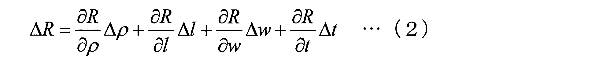
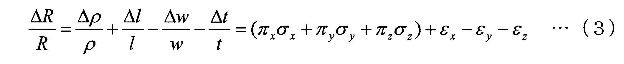
式(1)から式(3)において、ρはピエゾ抵抗の抵抗率、lはピエゾ抵抗の長さ、wはピエゾ抵抗の幅、tはピエゾ抵抗の厚さであり、σはピエゾ抵抗に誘起される応力、εはピエゾ抵抗に誘起される歪、πはピエゾ抵抗定数である。
また、式(1)から式(3)において、xはカンチレバーの長手方向、yはカンチレバーの横方向、zはカンチレバーの法線方向に対応する。
歪と応力の関係は、一般化されたHookeの法則から導くことが可能である。 In equations (1) to (3), ρ is the resistivity of the piezoresistor, l is the length of the piezoresistor, w is the width of the piezoresistor, t is the thickness of the piezoresistor, and σ is induced in the piezoresistor Is the strain induced by piezoresistance, and .pi. Is the piezoresistance constant.
In the equations (1) to (3), x corresponds to the longitudinal direction of the cantilever, y corresponds to the lateral direction of the cantilever, and z corresponds to the normal direction of the cantilever.
The relationship between strain and stress can be derived from the generalized Hooke's law.
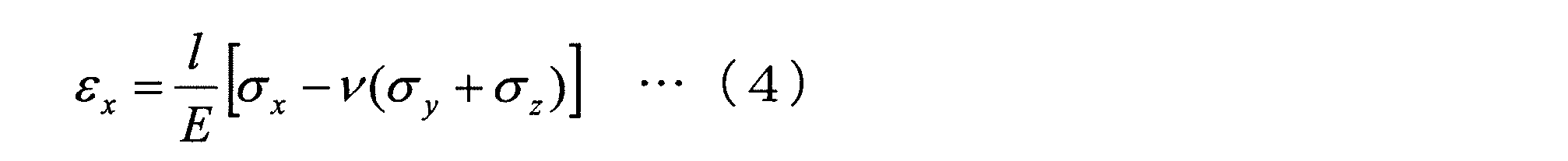

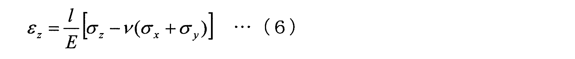
式(4)から式(6)において、EはカンチレバーのYoung率であり、νはカンチレバーのPoisson比である。したがって、平面応力である(すなわちσz=0)と仮定すれば、相対抵抗変化は、以下の式(7)で記述することが可能である。
In Equations (4) to (6), E is the Young's modulus of the cantilever, and ν is the Poisson's ratio of the cantilever. Therefore, assuming that it is a plane stress (ie, σ z = 0), the relative resistance change can be described by the following equation (7).
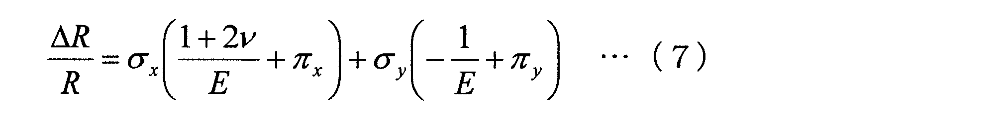
ここで、大きな信号を獲得し、シリコンが有する高いピエゾ係数を最大限利用するために、単結晶Si(100)を用いて形成されることで、p型半導体層を形成するピエゾ抵抗を検討する。ピエゾ抵抗係数は、以下の式(8)及び式(9)で示す関係によって決定される。
Here, in order to obtain a large signal and to make full use of the high piezo coefficient of silicon, the piezoresistor forming a p-type semiconductor layer is considered by being formed using single crystal Si (100). . The piezoresistance coefficient is determined by the relationships shown in the following equations (8) and (9).


式(8)及び式(9)において、π11、π12及びπ44は、結晶の基本ピエゾ抵抗係数である。x方向が[110]に整列したp型Si(100)であり、y方向が[1-10]に整列したp型Si(100)である場合は、π11が、10-11Pa-1を単位として+6.6である。これに加え、π12が、10-11Pa-1を単位として-1.1であり、π44が、10-11Pa-1を単位として+138.1である。
したがって、ピエゾ抵抗係数πxは、71.8×10⁻¹¹Pa-1と計算され、ピエゾ抵抗係数πyは、-66.3×10⁻¹¹Pa-1と計算される。また、Eは1.70×10¹¹Paであり、νは0.28である。そして、πx>>(1+2ν)/Eであり、πy>>-1/Eであり、πx≒-πy≒π44/2であるので、式(7)は、以下の式(10)で示すように近似することが可能である。 In equations (8) and (9), π11, π12 and π44 are the basic piezoresistive coefficients of the crystal. In the case where the x direction is p-type Si (100) aligned in [110] and the y direction is p-type Si (100) aligned in [1-10], π 11 is 10 −11 Pa −1 As +6.6. In addition to this, π12 is -1.1 in 10-11 Pa-1 as a unit, and π44 is +138.1 in 10-11 Pa-1 as a unit.
Therefore, the piezoresistance coefficient πx is calculated to be 71.8 × 10 11 Pa −1, and the piezoresistance coefficient πy is calculated to be −66.3 × 10 11 Pa −1. Further, E is 1.70 × 10 11 Pa and ν is 0.28. Then, since πx >> (1 + 2 + 2) / E, πy >> − 1 / E, and πx ≒ −πy ≒ π44 / 2, equation (7) can be expressed by equation (10) below. It is possible to approximate to
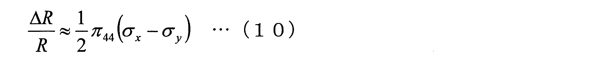
(表面応力センサの製造方法)
図1から図5を参照しつつ、図6から図12を用いて、表面応力センサ1の製造方法を説明する。なお、図6から図12は、図5のX-X線断面の位置に対応する断面図である。
表面応力センサ1の製造方法は、積層体形成工程と、第一イオン注入工程と、第二イオン注入工程と、熱処理工程と、配線層形成工程と、除去工程を備える。 (Method of manufacturing surface stress sensor)
A method of manufacturing thesurface stress sensor 1 will be described with reference to FIGS. 1 to 5 and with reference to FIGS. 6 to 12. 6 to 12 are cross-sectional views corresponding to the position of the cross section along line XX in FIG.
The method of manufacturing thesurface stress sensor 1 includes a laminate formation step, a first ion implantation step, a second ion implantation step, a heat treatment step, a wiring layer formation step, and a removal step.
図1から図5を参照しつつ、図6から図12を用いて、表面応力センサ1の製造方法を説明する。なお、図6から図12は、図5のX-X線断面の位置に対応する断面図である。
表面応力センサ1の製造方法は、積層体形成工程と、第一イオン注入工程と、第二イオン注入工程と、熱処理工程と、配線層形成工程と、除去工程を備える。 (Method of manufacturing surface stress sensor)
A method of manufacturing the
The method of manufacturing the
(積層体形成工程)
積層体形成工程では、まず、図6(a)に示すように、支持基材10の材料となる第一シリコン基板60の一方の面に、リソグラフィー及びエッチング技術を用いて凹部62(トレンチ)を形成する。凹部62の深さは、例えば、7[μm]に設定する。
次に、凹部62を形成した第一シリコン基板60に対し、検出基材20の材料となる第二シリコン基板64を、接着等、各種の接合技術を用いて貼り合わせることで、図6(b)に示すように、積層体66(Cavityウェーハ)を形成する。 (Laminate formation process)
In the laminated body forming step, first, as shown in FIG. 6A, a recess 62 (trench) is formed on one surface of thefirst silicon substrate 60 which is a material of the support base 10 using lithography and etching technology. Form. The depth of the recess 62 is set to, for example, 7 μm.
Next, asecond silicon substrate 64 as a material of the detection base 20 is bonded to the first silicon substrate 60 in which the recess 62 is formed by using various bonding techniques such as adhesion, as shown in FIG. The stack 66 (Cavity wafer) is formed as shown in FIG.
積層体形成工程では、まず、図6(a)に示すように、支持基材10の材料となる第一シリコン基板60の一方の面に、リソグラフィー及びエッチング技術を用いて凹部62(トレンチ)を形成する。凹部62の深さは、例えば、7[μm]に設定する。
次に、凹部62を形成した第一シリコン基板60に対し、検出基材20の材料となる第二シリコン基板64を、接着等、各種の接合技術を用いて貼り合わせることで、図6(b)に示すように、積層体66(Cavityウェーハ)を形成する。 (Laminate formation process)
In the laminated body forming step, first, as shown in FIG. 6A, a recess 62 (trench) is formed on one surface of the
Next, a
上記のように、積層体形成工程を行うことで、積層体66の所定の位置には、上下左右をシリコン(第一シリコン基板60、第二シリコン基板64)によって囲まれた空隙部40が形成される。
以上により、積層体形成工程では、支持基材10の一方の面に凹部62を形成し、さらに、支持基材10へ凹部62を覆うように検出基材20を貼り合わせることで、支持基材10と検出基材20との間に空隙部40が設けられた積層体66を形成する。 As described above, by performing the laminated body forming process, the void 40 surrounded by silicon (thefirst silicon substrate 60 and the second silicon substrate 64) is formed at the predetermined position of the laminated body 66. Be done.
As described above, in the laminate formation step, therecess 62 is formed on one surface of the support substrate 10, and the detection substrate 20 is bonded to the support substrate 10 so as to cover the recess 62. A laminated body 66 in which a gap 40 is provided between the sensor 10 and the detection base 20 is formed.
以上により、積層体形成工程では、支持基材10の一方の面に凹部62を形成し、さらに、支持基材10へ凹部62を覆うように検出基材20を貼り合わせることで、支持基材10と検出基材20との間に空隙部40が設けられた積層体66を形成する。 As described above, by performing the laminated body forming process, the void 40 surrounded by silicon (the
As described above, in the laminate formation step, the
(第一イオン注入工程)
第一イオン注入工程では、まず、図7に示すように、第二シリコン基板64の上側の面を酸化させて第一のシリコン酸化膜68aを形成し、フォトレジストのパターン(図示せず)を用いて、可撓性抵抗領域70に対し、選択的に第一のイオンを注入する。
以上により、第一イオン注入工程では、検出基材20の支持基材10と対向する面と反対側の面のうち、検出基材20の中心を含む予め設定した領域よりも外側の選択した一部の領域(可撓性抵抗領域70)に、第一のイオンを注入する。 (First ion implantation process)
In the first ion implantation step, first, as shown in FIG. 7, the upper surface of thesecond silicon substrate 64 is oxidized to form a first silicon oxide film 68a, and a photoresist pattern (not shown) is formed. Using this, the first ion is selectively implanted into the flexible resistance region 70.
As described above, in the first ion implantation step, one of the surfaces on the opposite side to the surface of thedetection base 20 opposite to the support base 10 is selected outside the preset region including the center of the detection base 20. First ions are implanted into the area of the part (flexible resistance area 70).
第一イオン注入工程では、まず、図7に示すように、第二シリコン基板64の上側の面を酸化させて第一のシリコン酸化膜68aを形成し、フォトレジストのパターン(図示せず)を用いて、可撓性抵抗領域70に対し、選択的に第一のイオンを注入する。
以上により、第一イオン注入工程では、検出基材20の支持基材10と対向する面と反対側の面のうち、検出基材20の中心を含む予め設定した領域よりも外側の選択した一部の領域(可撓性抵抗領域70)に、第一のイオンを注入する。 (First ion implantation process)
In the first ion implantation step, first, as shown in FIG. 7, the upper surface of the
As described above, in the first ion implantation step, one of the surfaces on the opposite side to the surface of the
(第二イオン注入工程)
第二イオン注入工程では、第一イオン注入工程で用いたフォトレジストを除去し、さらに、第一イオン注入工程で用いたものとは異なるフォトレジストのパターン(図示せず)を形成し、図7中に示すように、低抵抗領域72に第二のイオンを注入する。
以上により、第二イオン注入工程では、検出基材20の第一のイオンを注入した領域(可撓性抵抗領域70)よりも外側の選択した領域に、第二のイオンを注入する。 (Second ion implantation process)
In the second ion implantation step, the photoresist used in the first ion implantation step is removed, and a pattern (not shown) of a photoresist different from that used in the first ion implantation step is formed. As shown therein, a second ion is implanted into thelow resistance region 72.
As described above, in the second ion implantation step, the second ions are implanted into a selected region outside the region (flexible resistance region 70) into which the first ions of thedetection substrate 20 are implanted.
第二イオン注入工程では、第一イオン注入工程で用いたフォトレジストを除去し、さらに、第一イオン注入工程で用いたものとは異なるフォトレジストのパターン(図示せず)を形成し、図7中に示すように、低抵抗領域72に第二のイオンを注入する。
以上により、第二イオン注入工程では、検出基材20の第一のイオンを注入した領域(可撓性抵抗領域70)よりも外側の選択した領域に、第二のイオンを注入する。 (Second ion implantation process)
In the second ion implantation step, the photoresist used in the first ion implantation step is removed, and a pattern (not shown) of a photoresist different from that used in the first ion implantation step is formed. As shown therein, a second ion is implanted into the
As described above, in the second ion implantation step, the second ions are implanted into a selected region outside the region (flexible resistance region 70) into which the first ions of the
(熱処理工程)
熱処理工程では、第二イオン注入工程で用いたフォトレジストを除去し、さらに、第一のイオン及び第二のイオンの活性化を目的として、積層体66に熱処理(アニール処理)を施す。積層体66に熱処理を施した後は、第一のシリコン酸化膜68aを除去する。
以上により、熱処理工程では、第一のイオン及び第二のイオンを注入した積層体66を熱処理することで、第一のイオンを注入した領域に可撓性抵抗領域70を形成するとともに、第二のイオンを注入した領域に低抵抗領域72を形成する。 (Heat treatment process)
In the heat treatment step, the photoresist used in the second ion implantation step is removed, and a heat treatment (annealing treatment) is performed on thestacked body 66 for the purpose of activating the first ion and the second ion. After heat treatment is performed on the stacked body 66, the first silicon oxide film 68a is removed.
As described above, in the heat treatment step, the multilayerresistive element 66 into which the first ion and the second ion are implanted is heat treated to form the flexible resistance region 70 in the region into which the first ion is implanted. The low resistance region 72 is formed in the region into which the ions of.
熱処理工程では、第二イオン注入工程で用いたフォトレジストを除去し、さらに、第一のイオン及び第二のイオンの活性化を目的として、積層体66に熱処理(アニール処理)を施す。積層体66に熱処理を施した後は、第一のシリコン酸化膜68aを除去する。
以上により、熱処理工程では、第一のイオン及び第二のイオンを注入した積層体66を熱処理することで、第一のイオンを注入した領域に可撓性抵抗領域70を形成するとともに、第二のイオンを注入した領域に低抵抗領域72を形成する。 (Heat treatment process)
In the heat treatment step, the photoresist used in the second ion implantation step is removed, and a heat treatment (annealing treatment) is performed on the
As described above, in the heat treatment step, the multilayer
(配線層形成工程)
配線層形成工程では、図8(a)に示すように、第二シリコン基板64の上側の面に対し、シリコン窒化膜74と第二のシリコン酸化膜68bとを順に積層する。そして、通常のリソグラフィー及び酸化膜エッチングにより、図8(b)に示すように、第二のシリコン酸化膜68bへ、ホール76を形成する。
次に、図9(a)に示すように、第二のシリコン酸化膜68bの上へ、Ti及びTiNで形成した積層膜78をスパッタリングによって形成し、熱処理を施す。積層膜78は、Al等の金属膜がSiへ異常拡散することを防止する役割を持つ、いわゆるバリアメタルであり、熱処理を施すことによって、ホール76の底部に存在するSiとTiの界面がシリサイド化して、低抵抗な接続を形成することが可能となる。
さらに、図9(b)に示すように、積層膜78の上へ、スパッタリングによって、Al等の金属膜80を積層する。 (Wiring layer formation process)
In the wiring layer formation step, as shown in FIG. 8A, thesilicon nitride film 74 and the second silicon oxide film 68b are sequentially stacked on the upper surface of the second silicon substrate 64. Then, as shown in FIG. 8B, holes 76 are formed in the second silicon oxide film 68b by ordinary lithography and oxide film etching.
Next, as shown in FIG. 9A, alaminated film 78 formed of Ti and TiN is formed on the second silicon oxide film 68b by sputtering, and heat treatment is performed. The laminated film 78 is a so-called barrier metal having a role of preventing abnormal diffusion of a metal film such as Al into Si, and the interface between Si and Ti existing at the bottom of the hole 76 is silicided by heat treatment. To form a low resistance connection.
Further, as shown in FIG. 9B, ametal film 80 such as Al is laminated on the laminated film 78 by sputtering.
配線層形成工程では、図8(a)に示すように、第二シリコン基板64の上側の面に対し、シリコン窒化膜74と第二のシリコン酸化膜68bとを順に積層する。そして、通常のリソグラフィー及び酸化膜エッチングにより、図8(b)に示すように、第二のシリコン酸化膜68bへ、ホール76を形成する。
次に、図9(a)に示すように、第二のシリコン酸化膜68bの上へ、Ti及びTiNで形成した積層膜78をスパッタリングによって形成し、熱処理を施す。積層膜78は、Al等の金属膜がSiへ異常拡散することを防止する役割を持つ、いわゆるバリアメタルであり、熱処理を施すことによって、ホール76の底部に存在するSiとTiの界面がシリサイド化して、低抵抗な接続を形成することが可能となる。
さらに、図9(b)に示すように、積層膜78の上へ、スパッタリングによって、Al等の金属膜80を積層する。 (Wiring layer formation process)
In the wiring layer formation step, as shown in FIG. 8A, the
Next, as shown in FIG. 9A, a
Further, as shown in FIG. 9B, a
次に、フォトリソグラフィー及びエッチング技術を用いて金属膜80をパターニングすることにより、図10(a)に示すような配線層82を形成する。さらに、図10(b)に示すように、絶縁層として第三のシリコン酸化膜68cを積層する。
その後、図11(a)に示すように、可撓性抵抗領域70及び検出基材の中心を含む予め設定した領域(後にメンブレンとなる領域)であるメンブレン設定領域84以外を覆うようなフォトレジストのパターン(図示せず)を形成する。さらに、エッチング技術によって、可撓性抵抗領域70及びメンブレン設定領域84に形成されている第二のシリコン酸化膜68bを除去する。そして、メンブレン設定領域84以外を覆うようなフォトレジストのパターン(図示せず)を形成して、図11(b)に示すように、メンブレン設定領域84のシリコン窒化膜74を除去する。
次に、図12に示すように、可撓性抵抗50からの出力を得るためのPAD86を、通常のフォトリソグラフィー及びエッチング技術によって形成する。
以上により、配線層形成工程では、可撓性抵抗50と電気的に接続された配線層82を形成する。 Next, themetal film 80 is patterned by photolithography and etching to form a wiring layer 82 as shown in FIG. Further, as shown in FIG. 10B, a third silicon oxide film 68c is stacked as an insulating layer.
Thereafter, as shown in FIG. 11A, a photoresist which covers areas other than themembrane setting area 84 which is a predetermined area including the center of the flexible resistance area 70 and the detection base (area to be a membrane later). Form a pattern (not shown). Furthermore, the flexible resistance region 70 and the second silicon oxide film 68 b formed in the membrane setting region 84 are removed by the etching technique. Then, a photoresist pattern (not shown) which covers areas other than the membrane setting area 84 is formed, and as shown in FIG. 11B, the silicon nitride film 74 in the membrane setting area 84 is removed.
Next, as shown in FIG. 12, aPAD 86 for obtaining an output from the flexible resistor 50 is formed by the usual photolithography and etching techniques.
Thus, in the wiring layer formation step, thewiring layer 82 electrically connected to the flexible resistor 50 is formed.
その後、図11(a)に示すように、可撓性抵抗領域70及び検出基材の中心を含む予め設定した領域(後にメンブレンとなる領域)であるメンブレン設定領域84以外を覆うようなフォトレジストのパターン(図示せず)を形成する。さらに、エッチング技術によって、可撓性抵抗領域70及びメンブレン設定領域84に形成されている第二のシリコン酸化膜68bを除去する。そして、メンブレン設定領域84以外を覆うようなフォトレジストのパターン(図示せず)を形成して、図11(b)に示すように、メンブレン設定領域84のシリコン窒化膜74を除去する。
次に、図12に示すように、可撓性抵抗50からの出力を得るためのPAD86を、通常のフォトリソグラフィー及びエッチング技術によって形成する。
以上により、配線層形成工程では、可撓性抵抗50と電気的に接続された配線層82を形成する。 Next, the
Thereafter, as shown in FIG. 11A, a photoresist which covers areas other than the
Next, as shown in FIG. 12, a
Thus, in the wiring layer formation step, the
(除去工程)
除去工程では、メンブレン設定領域84の一部をエッチングにて切り取ることで、二対である四つの連結部26a~26dをパターニングする。
したがって、除去工程では、メンブレン設定領域84の周囲であって、低抵抗領域72及び可撓性抵抗領域70(後に連結部26となる領域)以外の領域を除去することで、メンブレン22、枠部材24、連結部26、可撓性抵抗50を形成する。 (Removal process)
In the removal step, a part of themembrane setting area 84 is cut away by etching to pattern two pairs of four connecting parts 26a to 26d.
Therefore, in the removing step, themembrane 22 and the frame member are removed by removing the area other than the low resistance area 72 and the flexible resistance area 70 (area to be the connection portion 26 later) around the membrane setting area 84. 24, forming the connecting portion 26 and the flexible resistor 50.
除去工程では、メンブレン設定領域84の一部をエッチングにて切り取ることで、二対である四つの連結部26a~26dをパターニングする。
したがって、除去工程では、メンブレン設定領域84の周囲であって、低抵抗領域72及び可撓性抵抗領域70(後に連結部26となる領域)以外の領域を除去することで、メンブレン22、枠部材24、連結部26、可撓性抵抗50を形成する。 (Removal process)
In the removal step, a part of the
Therefore, in the removing step, the
(動作・作用)
図1から図12を参照しつつ、図13及び図14を用いて、第一実施形態の動作と作用を説明する。
表面応力センサ1を、例えば、嗅覚センサとして用いる際には、臭い成分を含んだガスの雰囲気中に受容体30を配置し、ガスが含む臭い成分を、受容体30に吸着させる。
受容体30にガスの分子が吸着して、受容体30に歪みが発生すると、メンブレン22に表面応力が印加され、メンブレン22が撓む。
枠部材24は井桁状に形成されてメンブレン22を包囲しており、連結部26は、メンブレン22と枠部材24を両端部で連結している。このため、連結部26のうち、メンブレン22に連結している端部は自由端となっており、枠部材24に連結している端部は固定端となっている。 (Operation / action)
The operation and operation of the first embodiment will be described with reference to FIGS. 13 and 14 with reference to FIGS. 1 to 12.
When thesurface stress sensor 1 is used as, for example, an olfactory sensor, the receptor 30 is disposed in a gas atmosphere containing an odorous component, and the odorous component contained in the gas is adsorbed to the receptor 30.
When molecules of the gas are adsorbed to thereceptor 30 and distortion occurs in the receptor 30, surface stress is applied to the membrane 22, and the membrane 22 bends.
Theframe member 24 is formed in a cross-girder shape and surrounds the membrane 22, and the connection part 26 connects the membrane 22 and the frame member 24 at both ends. Therefore, the end of the connection portion 26 connected to the membrane 22 is a free end, and the end connected to the frame member 24 is a fixed end.
図1から図12を参照しつつ、図13及び図14を用いて、第一実施形態の動作と作用を説明する。
表面応力センサ1を、例えば、嗅覚センサとして用いる際には、臭い成分を含んだガスの雰囲気中に受容体30を配置し、ガスが含む臭い成分を、受容体30に吸着させる。
受容体30にガスの分子が吸着して、受容体30に歪みが発生すると、メンブレン22に表面応力が印加され、メンブレン22が撓む。
枠部材24は井桁状に形成されてメンブレン22を包囲しており、連結部26は、メンブレン22と枠部材24を両端部で連結している。このため、連結部26のうち、メンブレン22に連結している端部は自由端となっており、枠部材24に連結している端部は固定端となっている。 (Operation / action)
The operation and operation of the first embodiment will be described with reference to FIGS. 13 and 14 with reference to FIGS. 1 to 12.
When the
When molecules of the gas are adsorbed to the
The
したがって、メンブレン22が撓むと、連結部26に、受容体30に発生した歪みに応じた撓みが起きる。そして、連結部26に起きた撓みに応じて、可撓性抵抗50が有する抵抗値が変化し、抵抗値の変化に応じた電圧の変化がPAD86から出力され、コンピュータ等におけるデータ検出に用いられる。
表面応力センサ1の使用時には、例えば、表面応力センサ1の使用環境に発生した温度変化等により、パッケージ基板2が変形(収縮、伸長、反り)する可能性がある。 Therefore, when themembrane 22 bends, the connection portion 26 bends in response to the strain generated in the receiver 30. Then, the resistance value of the flexible resistor 50 changes in accordance with the bending occurring in the connecting portion 26, and a change in voltage corresponding to the change in the resistance value is output from the PAD 86 and used for data detection in a computer or the like. .
When thesurface stress sensor 1 is used, there is a possibility that the package substrate 2 may be deformed (shrink, stretch, warp) due to a temperature change or the like generated in the use environment of the surface stress sensor 1, for example.
表面応力センサ1の使用時には、例えば、表面応力センサ1の使用環境に発生した温度変化等により、パッケージ基板2が変形(収縮、伸長、反り)する可能性がある。 Therefore, when the
When the
従来の構成を備える表面応力センサ100の構造、すなわち、例えば、図13(a)中に示すように、支持基材10が筒状に形成されており、メンブレン22が中空に浮いた構造では、以下の問題が発生する。すなわち、従来の構成を備える表面応力センサ100では、図13(b)中に示すように、パッケージ基板2が変形(収縮)すると、パッケージ基板2の変形に伴って、支持基材10も変形する。そして、メンブレン22が中空に浮いており、メンブレン22とパッケージ基板2との間には、空間のみが存在しているため、支持基材10の変形が許容され、メンブレン22が大きく撓むこととなる。すなわち、パッケージ基板2の変形が、メンブレン22に応力として印可されることになる。これにより、可撓性抵抗50による電圧または電流の出力にオフセットが与えられてしまい、温度変化に応じてオフセットが変化してしまうために、表面応力センサ1の精度が劣化することとなる。
In the structure of the surface stress sensor 100 having the conventional structure, that is, for example, as shown in FIG. 13A, in the structure in which the support base 10 is formed in a cylindrical shape and the membrane 22 floats in the hollow, The following problems occur. That is, in the surface stress sensor 100 having the conventional configuration, as shown in FIG. 13B, when the package substrate 2 is deformed (contracted), the support substrate 10 is also deformed along with the deformation of the package substrate 2. . Since the membrane 22 floats in the air and only a space exists between the membrane 22 and the package substrate 2, deformation of the support base 10 is permitted, and the membrane 22 is largely bent. Become. That is, the deformation of the package substrate 2 is applied to the membrane 22 as a stress. As a result, an offset is given to the output of the voltage or current by the flexible resistor 50, and the offset is changed according to the temperature change, so that the accuracy of the surface stress sensor 1 is deteriorated.
したがって、従来の構成を備える表面応力センサ100では、変形したパッケージ基板2から受ける応力の変化により、メンブレン22が大きく変形して、表面応力センサ100の特性が変化する。このため、表面応力センサ100の検査時と実装時において、表面応力センサ100の特性が変化してしまい、表面応力センサ100の出荷時における検査や校正が困難となる。
Therefore, in the surface stress sensor 100 having the conventional configuration, the membrane 22 is largely deformed due to the change in stress received from the deformed package substrate 2, and the characteristics of the surface stress sensor 100 are changed. Therefore, the characteristics of the surface stress sensor 100 change during the inspection and mounting of the surface stress sensor 100, which makes inspection and calibration at the time of shipping the surface stress sensor 100 difficult.
これに対し、第一実施形態の表面応力センサ1であれば、図14(a)中に示すように、メンブレン22とパッケージ基板2との間に支持基材10が存在する。また、支持基材10が柱状に形成されているため、従来の構成を備える表面応力センサ100のように、支持基材10が筒状に形成されている構成と比較して、高い剛性を有している。
このため、第一実施形態の表面応力センサ1であれば、図14(b)中に示すように、パッケージ基板2が変形(収縮)した場合であっても、支持基材10が高い剛性を有するため、支持基材10の変形が抑制され、メンブレン22の撓みが抑制されることとなる。 On the other hand, in the case of thesurface stress sensor 1 of the first embodiment, as shown in FIG. 14A, the support base 10 is present between the membrane 22 and the package substrate 2. Further, since the support base 10 is formed in a columnar shape, it has high rigidity as compared with the configuration in which the support base 10 is formed in a cylindrical shape as in the surface stress sensor 100 having the conventional configuration. doing.
For this reason, in the case of thesurface stress sensor 1 of the first embodiment, as shown in FIG. 14B, even if the package substrate 2 is deformed (contracted), the supporting base 10 has high rigidity. Because of this, the deformation of the support base 10 is suppressed, and the deflection of the membrane 22 is suppressed.
このため、第一実施形態の表面応力センサ1であれば、図14(b)中に示すように、パッケージ基板2が変形(収縮)した場合であっても、支持基材10が高い剛性を有するため、支持基材10の変形が抑制され、メンブレン22の撓みが抑制されることとなる。 On the other hand, in the case of the
For this reason, in the case of the
また、第一実施形態の表面応力センサ1であれば、支持基材10が高い剛性を有するため、温度変化等に起因するパッケージ基板2の応力変化に鈍感となり、精度の高い安定したセンシングが可能となる。
また、第一実施形態の表面応力センサ1であれば、支持基材10が、温度変化等に起因するパッケージ基板2の応力変化に鈍感となり、パッケージ基板2の構成(強度、材料、厚さ等)の影響を受けにくい。このため、多種多様な構成のパッケージ基板2に対して用いることが可能となる。
さらに、第一実施形態の表面応力センサ1であれば、支持基材10の中心が、接続部4を配置する位置と重なっている。これに加え、支持基材10の面積が、接続部4の面積よりも大きい。 In the case of thesurface stress sensor 1 according to the first embodiment, since the support base 10 has high rigidity, it is insensitive to stress change of the package substrate 2 caused by temperature change etc., and stable sensing with high accuracy is possible. It becomes.
Further, in the case of thesurface stress sensor 1 of the first embodiment, the support base 10 is insensitive to stress change of the package substrate 2 caused by temperature change and the like, and the configuration of the package substrate 2 (strength, material, thickness, etc. Hard to be affected by For this reason, it becomes possible to use for package substrate 2 of various composition.
Furthermore, in the case of thesurface stress sensor 1 of the first embodiment, the center of the support base 10 overlaps the position where the connection portion 4 is disposed. In addition to this, the area of the support base 10 is larger than the area of the connection portion 4.
また、第一実施形態の表面応力センサ1であれば、支持基材10が、温度変化等に起因するパッケージ基板2の応力変化に鈍感となり、パッケージ基板2の構成(強度、材料、厚さ等)の影響を受けにくい。このため、多種多様な構成のパッケージ基板2に対して用いることが可能となる。
さらに、第一実施形態の表面応力センサ1であれば、支持基材10の中心が、接続部4を配置する位置と重なっている。これに加え、支持基材10の面積が、接続部4の面積よりも大きい。 In the case of the
Further, in the case of the
Furthermore, in the case of the
このため、接続部4を介して支持基材10へ伝達される、パッケージ基板2の変形によって発生する応力は、パッケージ基板2の全体で発生する応力と比較して低減されるため、支持基材10の変形が抑制され、メンブレン22の撓みが抑制されることとなる。
したがって、第一実施形態の構成であれば、パッケージ基板2の変形によってメンブレン22に印加される応力を低減させて、表面応力センサ1の測定精度が劣化することを抑制することが可能である。 Therefore, the stress generated by the deformation of thepackage substrate 2 transmitted to the support substrate 10 through the connection portion 4 is reduced compared to the stress generated in the entire package substrate 2, and hence the support substrate The deformation of 10 is suppressed, and the deflection of the membrane 22 is suppressed.
Therefore, with the configuration of the first embodiment, it is possible to reduce the stress applied to themembrane 22 by the deformation of the package substrate 2 and to suppress the deterioration of the measurement accuracy of the surface stress sensor 1.
したがって、第一実施形態の構成であれば、パッケージ基板2の変形によってメンブレン22に印加される応力を低減させて、表面応力センサ1の測定精度が劣化することを抑制することが可能である。 Therefore, the stress generated by the deformation of the
Therefore, with the configuration of the first embodiment, it is possible to reduce the stress applied to the
また、技術開発やビジネスへの適用が可能なIoT関連の情報を収集する上で、人間の五感に相当する情報をセンシングする技術に対し、五感のうち、視覚、聴覚及び触覚と比較して、必ずしも一般的ではない味覚と嗅覚のセンサに適用することが可能となる。
なお、上述した第一実施形態は、本発明の一例であり、本発明は、上述した第一実施形態に限定されることはなく、この実施形態以外の形態であっても、本発明に係る技術的思想を逸脱しない範囲であれば、設計等に応じて種々の変更が可能である。 In addition, when collecting IoT related information applicable to technology development and business, the technology of sensing information equivalent to human's five senses is compared with visual sense, auditory sense and tactile sense among the five senses. It becomes possible to apply to the sensor of the taste and the sense of smell which are not necessarily general.
The above-described first embodiment is an example of the present invention, and the present invention is not limited to the above-described first embodiment, and the embodiment according to the present invention is applicable to any form other than this embodiment. Various modifications can be made according to the design and the like without departing from the technical concept.
(第一実施形態の効果)
第一実施形態の表面応力センサ1であれば、以下に記載する効果を奏することが可能となる。
(1)印加された表面応力によって撓むメンブレン22と、メンブレン22を包囲する枠部材24と、メンブレン22と枠部材24とを連結する連結部26と、連結部26に起きた撓みに応じて抵抗値が変化する可撓性抵抗50を備える。さらに、枠部材24に接続され、メンブレン22の厚さ方向から見てメンブレン22と重なる支持基材10を備える。これに加え、メンブレン22と支持基材10との間に、空隙部40が設けられている。 (Effect of the first embodiment)
With thesurface stress sensor 1 of the first embodiment, the effects described below can be achieved.
(1) Themembrane 22 flexed by the applied surface stress, the frame member 24 surrounding the membrane 22, the connecting portion 26 connecting the membrane 22 and the frame member 24, and the deflection occurring in the connecting portion 26 The flexible resistor 50 has a variable resistance value. Furthermore, the support base 10 connected to the frame member 24 and overlapping with the membrane 22 when viewed from the thickness direction of the membrane 22 is provided. In addition to this, a gap 40 is provided between the membrane 22 and the support base 10.
第一実施形態の表面応力センサ1であれば、以下に記載する効果を奏することが可能となる。
(1)印加された表面応力によって撓むメンブレン22と、メンブレン22を包囲する枠部材24と、メンブレン22と枠部材24とを連結する連結部26と、連結部26に起きた撓みに応じて抵抗値が変化する可撓性抵抗50を備える。さらに、枠部材24に接続され、メンブレン22の厚さ方向から見てメンブレン22と重なる支持基材10を備える。これに加え、メンブレン22と支持基材10との間に、空隙部40が設けられている。 (Effect of the first embodiment)
With the
(1) The
このため、支持基材10が高い剛性を有する構成となり、温度変化等に起因するパッケージ基板2の応力変化に鈍感となり、精度の高い安定したセンシングが可能となる。
その結果、パッケージ基板2の変形によってメンブレン22に印加される応力を低減させて、測定精度の劣化を抑制することが可能な、表面応力センサ1を提供することが可能となる。
また、半導体プロセスによって作製した表面応力センサ1が、パッケージ等への組み立ての前後において特性が変化してしまうことを防止することが可能となる。さらに、表面応力センサ1自体の剛性を向上させることが可能であるため、ハンドリング時の破損等、取り扱いで発生する不具合を防止することが可能となる。 Therefore, thesupport base 10 is configured to have high rigidity, and is insensitive to stress change of the package substrate 2 caused by temperature change or the like, and stable sensing with high accuracy becomes possible.
As a result, it is possible to provide thesurface stress sensor 1 capable of suppressing the deterioration of the measurement accuracy by reducing the stress applied to the membrane 22 by the deformation of the package substrate 2.
In addition, it is possible to prevent the characteristic of thesurface stress sensor 1 manufactured by the semiconductor process from being changed before and after assembly into a package or the like. Furthermore, since it is possible to improve the rigidity of the surface stress sensor 1 itself, it is possible to prevent problems such as breakage during handling or the like that occur during handling.
その結果、パッケージ基板2の変形によってメンブレン22に印加される応力を低減させて、測定精度の劣化を抑制することが可能な、表面応力センサ1を提供することが可能となる。
また、半導体プロセスによって作製した表面応力センサ1が、パッケージ等への組み立ての前後において特性が変化してしまうことを防止することが可能となる。さらに、表面応力センサ1自体の剛性を向上させることが可能であるため、ハンドリング時の破損等、取り扱いで発生する不具合を防止することが可能となる。 Therefore, the
As a result, it is possible to provide the
In addition, it is possible to prevent the characteristic of the
(2)可撓性抵抗50が、メンブレン22が撓むことで連結部26に起きた撓みに応じて変化する抵抗値を有するピエゾ抵抗である。
その結果、ピエゾ抵抗に誘起されるX方向及びY方向への応力を用いて、ピエゾ抵抗の抵抗値の相対抵抗変化を検出することが可能となり、受容体30に、対象とする分子が吸着したか否かを判定することが可能となる。 (2) The flexible resistor 50 is a piezoresistor having a resistance value that changes in accordance with the deflection occurring in theconnection portion 26 when the membrane 22 flexes.
As a result, it becomes possible to detect the relative resistance change of the resistance value of the piezoresistor using the stress in the X direction and the Y direction induced by the piezoresistor, and the target molecule is adsorbed to thereceptor 30 It is possible to determine whether or not.
その結果、ピエゾ抵抗に誘起されるX方向及びY方向への応力を用いて、ピエゾ抵抗の抵抗値の相対抵抗変化を検出することが可能となり、受容体30に、対象とする分子が吸着したか否かを判定することが可能となる。 (2) The flexible resistor 50 is a piezoresistor having a resistance value that changes in accordance with the deflection occurring in the
As a result, it becomes possible to detect the relative resistance change of the resistance value of the piezoresistor using the stress in the X direction and the Y direction induced by the piezoresistor, and the target molecule is adsorbed to the
(3)メンブレン22と枠部材24とが、二対である四つの連結部26a~26dで連結されており、可撓性抵抗50が、四つの連結部26a~26dのそれぞれに備えられ、四つの可撓性抵抗50が、フルホイートストンブリッジを形成する。
R1とR3はX方向、R2とR4はY方向への撓みが大きいため、R1とR2、R3とR4ではそれぞれ相対抵抗変化が逆になる。印可電圧VBをR1とR2で分割する出力端子Voutの電圧は、増減が逆であるR1とR2の相乗効果を発揮して変化する。R3とR4での分割でも同じことが言える。両Vout電圧は変化の方向が逆であるので、結果として両Vout電圧は足し合わされ、4つのピエゾ抵抗の変化は全てプラスに貢献して感度を高めるという点で、フルホイートストンブリッジは有利である。 (3) Themembrane 22 and the frame member 24 are connected by four pairs of four connecting portions 26a to 26d, and the flexible resistor 50 is provided at each of the four connecting portions 26a to 26d. Two flexible resistors 50 form a full Wheatstone bridge.
Since R1 and R3 have large deflection in the X direction, and R2 and R4 have large deflection in the Y direction, the relative resistance changes in R1 and R2 and R3 and R4 are reversed. The voltage of the output terminal Vout that divides the applied voltage VB by R1 and R2 changes by exhibiting the synergetic effect of R1 and R2 whose increase and decrease are opposite. The same is true for the splits in R3 and R4. The full Voutston bridge is advantageous in that both Vout voltages are reversed, so that both Vout voltages add as a result and all four piezoresistor changes contribute positively to increase sensitivity.
R1とR3はX方向、R2とR4はY方向への撓みが大きいため、R1とR2、R3とR4ではそれぞれ相対抵抗変化が逆になる。印可電圧VBをR1とR2で分割する出力端子Voutの電圧は、増減が逆であるR1とR2の相乗効果を発揮して変化する。R3とR4での分割でも同じことが言える。両Vout電圧は変化の方向が逆であるので、結果として両Vout電圧は足し合わされ、4つのピエゾ抵抗の変化は全てプラスに貢献して感度を高めるという点で、フルホイートストンブリッジは有利である。 (3) The
Since R1 and R3 have large deflection in the X direction, and R2 and R4 have large deflection in the Y direction, the relative resistance changes in R1 and R2 and R3 and R4 are reversed. The voltage of the output terminal Vout that divides the applied voltage VB by R1 and R2 changes by exhibiting the synergetic effect of R1 and R2 whose increase and decrease are opposite. The same is true for the splits in R3 and R4. The full Voutston bridge is advantageous in that both Vout voltages are reversed, so that both Vout voltages add as a result and all four piezoresistor changes contribute positively to increase sensitivity.
(4)メンブレン22がn型半導体層であり、可撓性抵抗50がp型半導体層である。
その結果、可撓性抵抗50に流れる電流はメンブレン22に流れることはなく、出力電圧にノイズが生じることはない。また、可撓性抵抗50にp型半導体を用いることで、n型を用いるよりも高い感度を実現することが可能となる。
(5)検出基材20を形成する材料と、支持基材10を形成する材料とが、同一の材料である。
その結果、温度変化等に起因するパッケージ基板2の変形に応じた、検出基材20の変形量と支持基材10の変形量との差を減少させることが可能となり、メンブレン22の撓みを抑制することが可能となる。 (4) Themembrane 22 is an n-type semiconductor layer, and the flexible resistor 50 is a p-type semiconductor layer.
As a result, the current flowing in the flexible resistor 50 does not flow in themembrane 22, and no noise is generated in the output voltage. In addition, by using a p-type semiconductor for the flexible resistor 50, it is possible to realize higher sensitivity than using n-type.
(5) The material forming thedetection base 20 and the material forming the support base 10 are the same material.
As a result, it becomes possible to reduce the difference between the amount of deformation of thedetection base 20 and the amount of deformation of the support base 10 in response to the deformation of the package substrate 2 caused by temperature change etc. It is possible to
その結果、可撓性抵抗50に流れる電流はメンブレン22に流れることはなく、出力電圧にノイズが生じることはない。また、可撓性抵抗50にp型半導体を用いることで、n型を用いるよりも高い感度を実現することが可能となる。
(5)検出基材20を形成する材料と、支持基材10を形成する材料とが、同一の材料である。
その結果、温度変化等に起因するパッケージ基板2の変形に応じた、検出基材20の変形量と支持基材10の変形量との差を減少させることが可能となり、メンブレン22の撓みを抑制することが可能となる。 (4) The
As a result, the current flowing in the flexible resistor 50 does not flow in the
(5) The material forming the
As a result, it becomes possible to reduce the difference between the amount of deformation of the
(6)支持基材10の線膨張係数が、5.0×10⁻⁶/℃以下である。
その結果、支持基材10の剛性を向上させることが可能となり、温度変化等に起因するパッケージ基板2の変形に対する、検出基材20の変形量を減少させることが可能となる。
(7)支持基材10の厚さが、80μm以上である。
その結果、支持基材10の剛性を向上させることが可能となり、温度変化等に起因するパッケージ基板2の変形に対する、検出基材20の変形量を減少させることが可能となる。 (6) The linear expansion coefficient of thesupport base 10 is 5.0 × 10 −6 / ° C. or less.
As a result, the rigidity of thesupport base 10 can be improved, and the amount of deformation of the detection base 20 with respect to the deformation of the package substrate 2 caused by a temperature change or the like can be reduced.
(7) The thickness of thesupport substrate 10 is 80 μm or more.
As a result, the rigidity of thesupport base 10 can be improved, and the amount of deformation of the detection base 20 with respect to the deformation of the package substrate 2 caused by a temperature change or the like can be reduced.
その結果、支持基材10の剛性を向上させることが可能となり、温度変化等に起因するパッケージ基板2の変形に対する、検出基材20の変形量を減少させることが可能となる。
(7)支持基材10の厚さが、80μm以上である。
その結果、支持基材10の剛性を向上させることが可能となり、温度変化等に起因するパッケージ基板2の変形に対する、検出基材20の変形量を減少させることが可能となる。 (6) The linear expansion coefficient of the
As a result, the rigidity of the
(7) The thickness of the
As a result, the rigidity of the
(8)メンブレン22の厚さ方向から見て、支持基材10の外周面と、枠部材24の外周面とが面一である。
その結果、通常の半導体製造で用いられるダイシング装置を使用して個片化することが可能となる。
(9)支持基材10が、ケイ素、サファイア、ガリウムヒ素、ガラス、石英のうちいずれかを含む材料で形成されている。
その結果、表面応力センサ1に要求される導電率を確保することが容易となる。 (8) When viewed from the thickness direction of themembrane 22, the outer peripheral surface of the support base 10 and the outer peripheral surface of the frame member 24 are flush with each other.
As a result, it is possible to singulate using a dicing apparatus used in ordinary semiconductor manufacturing.
(9) Thesupport substrate 10 is formed of a material containing any of silicon, sapphire, gallium arsenide, glass, and quartz.
As a result, it becomes easy to secure the conductivity required of thesurface stress sensor 1.
その結果、通常の半導体製造で用いられるダイシング装置を使用して個片化することが可能となる。
(9)支持基材10が、ケイ素、サファイア、ガリウムヒ素、ガラス、石英のうちいずれかを含む材料で形成されている。
その結果、表面応力センサ1に要求される導電率を確保することが容易となる。 (8) When viewed from the thickness direction of the
As a result, it is possible to singulate using a dicing apparatus used in ordinary semiconductor manufacturing.
(9) The
As a result, it becomes easy to secure the conductivity required of the
(10)支持基材10のメンブレン22と対向する面と反対側の面に接続されるパッケージ基板2をさらに備える。
その結果、表面応力センサ1の、各種のセンサへの実装が容易となる。
(11)支持基材10とパッケージ基板2とは、メンブレン22の厚さ方向から見てメンブレン22の少なくとも一部と重なる位置に配置された接続部4によって接続されている。
その結果、ブラケット等を用いることなく、支持基材10とパッケージ基板2を接続することが可能となり、構成の複雑化を抑制することが可能となる。 (10) The semiconductor device further includes thepackage substrate 2 connected to the surface opposite to the surface facing the membrane 22 of the support substrate 10.
As a result, mounting of thesurface stress sensor 1 on various sensors becomes easy.
(11) The supportingbase 10 and the package substrate 2 are connected by the connecting portion 4 disposed at a position overlapping at least a part of the membrane 22 when viewed in the thickness direction of the membrane 22.
As a result, it is possible to connect thesupport base 10 and the package substrate 2 without using a bracket or the like, and it is possible to suppress the complication of the configuration.
その結果、表面応力センサ1の、各種のセンサへの実装が容易となる。
(11)支持基材10とパッケージ基板2とは、メンブレン22の厚さ方向から見てメンブレン22の少なくとも一部と重なる位置に配置された接続部4によって接続されている。
その結果、ブラケット等を用いることなく、支持基材10とパッケージ基板2を接続することが可能となり、構成の複雑化を抑制することが可能となる。 (10) The semiconductor device further includes the
As a result, mounting of the
(11) The supporting
As a result, it is possible to connect the
(12)メンブレン22の厚さ方向から見て、接続部4の面積がメンブレン22の面積よりも小さい。
このため、接続部4を介して支持基材10へ伝達される、パッケージ基板2の変形によって発生する応力を、パッケージ基板2の全体で発生する応力よりも低減することが可能となる。
その結果、支持基材10の変形を抑制して、メンブレン22の撓みが抑制することが可能となる。
また、第一実施形態の表面応力センサの製造方法であれば、以下に記載する効果を奏することが可能となる。 (12) The area of theconnection portion 4 is smaller than the area of the membrane 22 when viewed in the thickness direction of the membrane 22.
For this reason, it is possible to reduce the stress generated by the deformation of thepackage substrate 2 transmitted to the support base 10 through the connection portion 4 more than the stress generated in the entire package substrate 2.
As a result, it is possible to suppress the deformation of thesupport substrate 10 and to suppress the deflection of the membrane 22.
Moreover, if it is a manufacturing method of the surface stress sensor of a first embodiment, it will become possible to produce an effect indicated below.
このため、接続部4を介して支持基材10へ伝達される、パッケージ基板2の変形によって発生する応力を、パッケージ基板2の全体で発生する応力よりも低減することが可能となる。
その結果、支持基材10の変形を抑制して、メンブレン22の撓みが抑制することが可能となる。
また、第一実施形態の表面応力センサの製造方法であれば、以下に記載する効果を奏することが可能となる。 (12) The area of the
For this reason, it is possible to reduce the stress generated by the deformation of the
As a result, it is possible to suppress the deformation of the
Moreover, if it is a manufacturing method of the surface stress sensor of a first embodiment, it will become possible to produce an effect indicated below.
(13)積層体形成工程と、第一イオン注入工程と、第二イオン注入工程と、熱処理工程と、配線層形成工程と、除去工程とを備える。積層体形成工程では、支持基材10の一方の面に凹部62を形成し、さらに、支持基材10へ凹部62を覆うように検出基材20を貼り合わせることで、支持基材10と検出基材20との間に空隙部40が設けられた積層体66を形成する。第一イオン注入工程では、検出基材20の支持基材10と対向する面と反対側の面のうち検出基材20の中心を含む予め設定した領域よりも外側の選択した一部の領域に、第一のイオンを注入する。第二イオン注入工程では、検出基材20の第一のイオンを注入した領域よりも外側の選択した領域に第二のイオンを注入する。熱処理工程では、第一のイオン及び第二のイオンを注入した積層体66を熱処理することで、第一のイオンを注入した領域に可撓性抵抗領域70を形成するとともに、第二のイオンを注入した領域に低抵抗領域72を形成する。配線層形成工程では、可撓性抵抗50と電気的に接続された配線層82を形成する。除去工程では、検出基材20の中心を含む予め設定した領域の周囲であって低抵抗領域72及び可撓性抵抗領域70以外の領域を除去することで、メンブレン22、枠部材24、連結部26及び可撓性抵抗50を形成する。
(13) A laminate formation step, a first ion implantation step, a second ion implantation step, a heat treatment step, a wiring layer formation step, and a removal step are provided. In the laminate forming step, the concave portion 62 is formed on one surface of the support base 10, and the detection base 20 is attached to the support base 10 so as to cover the concave portion 62, thereby detecting the support base 10 and the detection base 20. A laminate 66 in which the air gap 40 is provided between the substrate 20 is formed. In the first ion implantation step, of the surface opposite to the surface facing the support substrate 10 of the detection substrate 20, a selected partial region outside the preset region including the center of the detection substrate 20 , Inject the first ion. In the second ion implantation step, second ions are implanted into a selected region outside the region of the detection substrate 20 where the first ions are implanted. In the heat treatment step, the laminate 66 in which the first ion and the second ion are implanted is heat treated to form the flexible resistance region 70 in the region where the first ion is implanted, and the second ion. A low resistance region 72 is formed in the implanted region. In the wiring layer formation step, the wiring layer 82 electrically connected to the flexible resistor 50 is formed. In the removing step, the membrane 22, the frame member 24, and the connecting portion are removed by removing a region other than the low resistance region 72 and the flexible resistance region 70 around a preset region including the center of the detection substrate 20. 26 and form a flexible resistor 50.
このため、支持基材10が高い剛性を有する構成となり、温度変化等に起因するパッケージ基板2の応力変化に鈍感となり、精度の高い安定したセンシングが可能となる。
その結果、パッケージ基板2の変形によってメンブレン22に印加される応力を低減させて、測定精度の劣化を抑制することが可能な、表面応力センサの製造方法を提供することが可能となる。
また、半導体プロセスによって作製した表面応力センサ1が、パッケージ等への組み立ての前後において特性が変化してしまうことを防止することが可能となる。さらに、表面応力センサ1自体の剛性を向上させることが可能であるため、ハンドリング時の破損等、取り扱いで発生する不具合を防止することが可能となる。 Therefore, thesupport base 10 is configured to have high rigidity, and is insensitive to stress change of the package substrate 2 caused by temperature change or the like, and stable sensing with high accuracy becomes possible.
As a result, it is possible to provide a method of manufacturing a surface stress sensor capable of reducing the stress applied to themembrane 22 by the deformation of the package substrate 2 and suppressing the deterioration of the measurement accuracy.
In addition, it is possible to prevent the characteristic of thesurface stress sensor 1 manufactured by the semiconductor process from being changed before and after assembly into a package or the like. Furthermore, since it is possible to improve the rigidity of the surface stress sensor 1 itself, it is possible to prevent problems such as breakage during handling or the like that occur during handling.
その結果、パッケージ基板2の変形によってメンブレン22に印加される応力を低減させて、測定精度の劣化を抑制することが可能な、表面応力センサの製造方法を提供することが可能となる。
また、半導体プロセスによって作製した表面応力センサ1が、パッケージ等への組み立ての前後において特性が変化してしまうことを防止することが可能となる。さらに、表面応力センサ1自体の剛性を向上させることが可能であるため、ハンドリング時の破損等、取り扱いで発生する不具合を防止することが可能となる。 Therefore, the
As a result, it is possible to provide a method of manufacturing a surface stress sensor capable of reducing the stress applied to the
In addition, it is possible to prevent the characteristic of the
(第一実施形態の変形例)
(1)第一実施形態では、支持基材10の材料となる第一シリコン基板60の一方の面に凹部62を形成することで、メンブレン22と支持基材10との間に空隙部40を形成したが、これに限定するものではない。すなわち、検出基材20の材料となる第二シリコン基板64の支持基材10と対向する面に凹部を形成することで、メンブレン22と支持基材10との間に空隙部40を形成してもよい。
(2)第一実施形態では、二対である四つの連結部26a~26dに、それぞれ、可撓性抵抗50a~50dが備えられている構成としたが、これに限定するものではない。すなわち、一対である二つの連結部26に、それぞれ、可撓性抵抗50が備えられている構成としてもよい。 (Modification of the first embodiment)
(1) In the first embodiment, theconcave portion 62 is formed on one surface of the first silicon substrate 60 which is a material of the support base 10, whereby the air gap 40 is formed between the membrane 22 and the support base 10. Although formed, it is not limited to this. That is, a void is formed between the membrane 22 and the support base 10 by forming a recess on the surface of the second silicon substrate 64, which is the material of the detection base 20, facing the support base 10. It is also good.
(2) In the first embodiment, theflexible resistors 50a to 50d are respectively provided in the two pairs of four connecting parts 26a to 26d, but the present invention is not limited to this. That is, the flexible resistors 50 may be provided in each of the two connecting portions 26 which are a pair.
(1)第一実施形態では、支持基材10の材料となる第一シリコン基板60の一方の面に凹部62を形成することで、メンブレン22と支持基材10との間に空隙部40を形成したが、これに限定するものではない。すなわち、検出基材20の材料となる第二シリコン基板64の支持基材10と対向する面に凹部を形成することで、メンブレン22と支持基材10との間に空隙部40を形成してもよい。
(2)第一実施形態では、二対である四つの連結部26a~26dに、それぞれ、可撓性抵抗50a~50dが備えられている構成としたが、これに限定するものではない。すなわち、一対である二つの連結部26に、それぞれ、可撓性抵抗50が備えられている構成としてもよい。 (Modification of the first embodiment)
(1) In the first embodiment, the
(2) In the first embodiment, the
(3)第一実施形態では、四つの連結部26a~26dの全てに可撓性抵抗50が備えられている構成としたが、これに限定するものではなく、少なくとも一つの連結部26に可撓性抵抗50が備えられている構成としてもよい。
(4)第一実施形態では、接続部4の面積を、メンブレン22の厚さ方向から見て、メンブレン22の面積よりも小さい値としたが、これに限定するものではなく、接続部4の面積を、メンブレン22の面積以上としてもよい。
(5)第一実施形態では、接続部4の形状を円形としたが、これに限定するものではなく、接続部4の形状を、例えば、方形としてもよい。また、接続部4を、複数形成してもよい。 (3) In the first embodiment, the flexible resistor 50 is provided in all the four connectingportions 26a to 26d. However, the present invention is not limited to this. The flexible resistor 50 may be provided.
(4) In the first embodiment, the area of theconnection portion 4 is smaller than the area of the membrane 22 when viewed from the thickness direction of the membrane 22. However, the present invention is not limited to this. The area may be equal to or larger than the area of the membrane 22.
(5) In the first embodiment, the shape of theconnection portion 4 is circular, but it is not limited to this. For example, the shape of the connection portion 4 may be square. Also, a plurality of connection portions 4 may be formed.
(4)第一実施形態では、接続部4の面積を、メンブレン22の厚さ方向から見て、メンブレン22の面積よりも小さい値としたが、これに限定するものではなく、接続部4の面積を、メンブレン22の面積以上としてもよい。
(5)第一実施形態では、接続部4の形状を円形としたが、これに限定するものではなく、接続部4の形状を、例えば、方形としてもよい。また、接続部4を、複数形成してもよい。 (3) In the first embodiment, the flexible resistor 50 is provided in all the four connecting
(4) In the first embodiment, the area of the
(5) In the first embodiment, the shape of the
(6)第一実施形態では、検出基材20を形成する材料と、支持基材10を形成する材料とを、同一の材料としたが、これに限定するものではなく、検出基材20を形成する材料と、支持基材10を形成する材料とを、異なる材料としてもよい。
この場合、検出基材20の線膨張係数と支持基材10の線膨張係数との差を、1.2×10⁻⁵/℃以下することで、パッケージ基板2の変形に応じた、検出基材20の変形量と支持基材10の変形量との差を減少させることが可能となる。これにより、メンブレン22の撓みを抑制することが可能となる。 (6) In the first embodiment, the material for forming thedetection base 20 and the material for forming the support base 10 are the same material, but the present invention is not limited to this. The material to be formed and the material to form the support substrate 10 may be different materials.
In this case, by setting the difference between the linear expansion coefficient of thedetection base 20 and the linear expansion coefficient of the support base 10 to 1.2 × 10 −5 / ° C. or less, the detection base according to the deformation of the package substrate 2 It is possible to reduce the difference between the amount of deformation of the material 20 and the amount of deformation of the support substrate 10. This makes it possible to suppress the deflection of the membrane 22.
この場合、検出基材20の線膨張係数と支持基材10の線膨張係数との差を、1.2×10⁻⁵/℃以下することで、パッケージ基板2の変形に応じた、検出基材20の変形量と支持基材10の変形量との差を減少させることが可能となる。これにより、メンブレン22の撓みを抑制することが可能となる。 (6) In the first embodiment, the material for forming the
In this case, by setting the difference between the linear expansion coefficient of the
(7)第一実施形態では、支持基材10の線膨張係数が、5.0×10⁻⁶/℃以下としたが、これに限定するものではなく、支持基材10の線膨張係数を、1.0×10-5/℃以下としてもよい。
この場合であっても、支持基材10の剛性を向上させることが可能となり、温度変化等
に起因するパッケージ基板2の変形に対する、検出基材20の変形量を減少させることが可能となる。 (7) In the first embodiment, although the linear expansion coefficient of thesupport base 10 is 5.0 × 10 −6 / ° C. or less, the present invention is not limited to this, and the linear expansion coefficient of the support base 10 is Or less than 1.0 × 10 −5 / ° C.
Even in this case, the rigidity of thesupport base 10 can be improved, and the amount of deformation of the detection base 20 with respect to the deformation of the package substrate 2 caused by a temperature change or the like can be reduced.
この場合であっても、支持基材10の剛性を向上させることが可能となり、温度変化等
に起因するパッケージ基板2の変形に対する、検出基材20の変形量を減少させることが可能となる。 (7) In the first embodiment, although the linear expansion coefficient of the
Even in this case, the rigidity of the
(第二実施形態)
以下、本発明の第二実施形態について、図面を参照しつつ説明する。
(構成)
図1から図5を参照しつつ、図15を用いて、第二実施形態の構成を説明する。
第二実施形態の構成は、図15に示すように、枠部材24が、接続層90を介して、支持基材10のパッケージ基板2と対向する面と反対側の面(図15中では、上側の面)に接続されている点を除き、上述した第一実施形態と同様である。
接続層90は、二酸化ケイ素(SiO2)等を用いて形成されている。
その他の構成は、上述した第一実施形態と同様であるため、説明を省略する。 Second Embodiment
Hereinafter, a second embodiment of the present invention will be described with reference to the drawings.
(Constitution)
The configuration of the second embodiment will be described using FIG. 15 with reference to FIGS. 1 to 5.
According to the configuration of the second embodiment, as shown in FIG. 15, theframe member 24 has a surface on the opposite side to the surface of the support base 10 facing the package substrate 2 via the connection layer 90 (in FIG. It is the same as the first embodiment described above except that it is connected to the upper surface).
Theconnection layer 90 is formed using silicon dioxide (SiO 2 ) or the like.
The other configuration is the same as that of the first embodiment described above, so the description will be omitted.
以下、本発明の第二実施形態について、図面を参照しつつ説明する。
(構成)
図1から図5を参照しつつ、図15を用いて、第二実施形態の構成を説明する。
第二実施形態の構成は、図15に示すように、枠部材24が、接続層90を介して、支持基材10のパッケージ基板2と対向する面と反対側の面(図15中では、上側の面)に接続されている点を除き、上述した第一実施形態と同様である。
接続層90は、二酸化ケイ素(SiO2)等を用いて形成されている。
その他の構成は、上述した第一実施形態と同様であるため、説明を省略する。 Second Embodiment
Hereinafter, a second embodiment of the present invention will be described with reference to the drawings.
(Constitution)
The configuration of the second embodiment will be described using FIG. 15 with reference to FIGS. 1 to 5.
According to the configuration of the second embodiment, as shown in FIG. 15, the
The
The other configuration is the same as that of the first embodiment described above, so the description will be omitted.
(表面応力センサの製造方法)
図1から図15を参照しつつ、図16から図19を用いて、表面応力センサ1の製造方法を説明する。なお、図16から図19の断面図は、図5のX-X線断面図に対応する。
表面応力センサ1の製造方法は、積層体形成工程と、第一イオン注入工程と、第二イオン注入工程と、熱処理工程と、ホール形成工程と、空隙部形成工程と、ホール封止工程と、配線層形成工程と、除去工程を備える。 (Method of manufacturing surface stress sensor)
A method of manufacturing thesurface stress sensor 1 will be described with reference to FIGS. 16 to 19 with reference to FIGS. 1 to 15. The cross-sectional views of FIGS. 16 to 19 correspond to the cross-sectional views of FIG. 5 along the line XX.
The method of manufacturing thesurface stress sensor 1 includes a laminate forming step, a first ion implantation step, a second ion implantation step, a heat treatment step, a hole forming step, a void forming step, a hole sealing step, A wiring layer forming step and a removing step are provided.
図1から図15を参照しつつ、図16から図19を用いて、表面応力センサ1の製造方法を説明する。なお、図16から図19の断面図は、図5のX-X線断面図に対応する。
表面応力センサ1の製造方法は、積層体形成工程と、第一イオン注入工程と、第二イオン注入工程と、熱処理工程と、ホール形成工程と、空隙部形成工程と、ホール封止工程と、配線層形成工程と、除去工程を備える。 (Method of manufacturing surface stress sensor)
A method of manufacturing the
The method of manufacturing the
(積層体形成工程)
積層体形成工程では、まず、図16に示すように、支持基材10の材料となる第一シリコン基板60へ、シリコン酸化膜を用いて形成した犠牲層92を積層する。さらに、犠牲層92へ、検出基材20の材料となる第二シリコン基板64を積層する。なお、犠牲層92としては、シリコン酸化膜の他に、シリコン窒化膜やアルミニウム、チタン、銅、タングステン等の金属膜を用いてもよい。
以上により、積層体形成工程では、支持基材10に犠牲層92を積層し、さらに、犠牲層92に検出基材20を積層して積層体66を形成する。 (Laminate formation process)
In the laminate formation step, first, as shown in FIG. 16, asacrificial layer 92 formed using a silicon oxide film is laminated on a first silicon substrate 60 which is a material of the support base 10. Furthermore, a second silicon substrate 64 which is a material of the detection base 20 is stacked on the sacrificial layer 92. As the sacrificial layer 92, in addition to the silicon oxide film, a silicon nitride film or a metal film such as aluminum, titanium, copper, tungsten or the like may be used.
As described above, in the laminate formation step, thesacrificial layer 92 is laminated on the support substrate 10, and the detection substrate 20 is further laminated on the sacrificial layer 92 to form a laminate 66.
積層体形成工程では、まず、図16に示すように、支持基材10の材料となる第一シリコン基板60へ、シリコン酸化膜を用いて形成した犠牲層92を積層する。さらに、犠牲層92へ、検出基材20の材料となる第二シリコン基板64を積層する。なお、犠牲層92としては、シリコン酸化膜の他に、シリコン窒化膜やアルミニウム、チタン、銅、タングステン等の金属膜を用いてもよい。
以上により、積層体形成工程では、支持基材10に犠牲層92を積層し、さらに、犠牲層92に検出基材20を積層して積層体66を形成する。 (Laminate formation process)
In the laminate formation step, first, as shown in FIG. 16, a
As described above, in the laminate formation step, the
(第一イオン注入工程)
第一イオン注入工程では、まず、図16に示すように、第二シリコン基板64を酸化することで、第二シリコン基板64の上側の面を酸化させて第一のシリコン酸化膜68aを形成する。
次に、第一のシリコン酸化膜68aを形成した第二シリコン基板64に対して、フォトレジストのパターン(図示せず)を形成し、可撓性抵抗領域70に対して、選択的に第一のイオンを注入する。
以上により、第一イオン注入工程では、検出基材20の支持基材10と対向する面と反対側の面のうち、検出基材20の中心を含む予め設定した領域よりも外側の選択した一部の領域(可撓性抵抗領域70)に、第一のイオンを注入する。 (First ion implantation process)
In the first ion implantation step, first, as shown in FIG. 16, thesecond silicon substrate 64 is oxidized to oxidize the upper surface of the second silicon substrate 64 to form a first silicon oxide film 68a. .
Next, a photoresist pattern (not shown) is formed on thesecond silicon substrate 64 on which the first silicon oxide film 68 a is formed, and Implant ions.
As described above, in the first ion implantation step, one of the surfaces on the opposite side to the surface of thedetection base 20 opposite to the support base 10 is selected outside the preset region including the center of the detection base 20. First ions are implanted into the area of the part (flexible resistance area 70).
第一イオン注入工程では、まず、図16に示すように、第二シリコン基板64を酸化することで、第二シリコン基板64の上側の面を酸化させて第一のシリコン酸化膜68aを形成する。
次に、第一のシリコン酸化膜68aを形成した第二シリコン基板64に対して、フォトレジストのパターン(図示せず)を形成し、可撓性抵抗領域70に対して、選択的に第一のイオンを注入する。
以上により、第一イオン注入工程では、検出基材20の支持基材10と対向する面と反対側の面のうち、検出基材20の中心を含む予め設定した領域よりも外側の選択した一部の領域(可撓性抵抗領域70)に、第一のイオンを注入する。 (First ion implantation process)
In the first ion implantation step, first, as shown in FIG. 16, the
Next, a photoresist pattern (not shown) is formed on the
As described above, in the first ion implantation step, one of the surfaces on the opposite side to the surface of the
(第二イオン注入工程)
第二イオン注入工程では、第一イオン注入工程で用いたフォトレジストを除去し、さらに、第一イオン注入工程で用いたものとは異なるフォトレジストのパターン(図示せず)を形成し、低抵抗領域72に第二のイオンを注入する。
以上により、第二イオン注入工程では、検出基材20の第一のイオンを注入した領域(可撓性抵抗領域70)よりも外側の選択した領域に、第二のイオンを注入する。 (Second ion implantation process)
In the second ion implantation step, the photoresist used in the first ion implantation step is removed, and a pattern (not shown) of a photoresist different from that used in the first ion implantation step is formed to reduce theresistance Region 72 is implanted with a second ion.
As described above, in the second ion implantation step, the second ions are implanted into a selected region outside the region (flexible resistance region 70) into which the first ions of thedetection substrate 20 are implanted.
第二イオン注入工程では、第一イオン注入工程で用いたフォトレジストを除去し、さらに、第一イオン注入工程で用いたものとは異なるフォトレジストのパターン(図示せず)を形成し、低抵抗領域72に第二のイオンを注入する。
以上により、第二イオン注入工程では、検出基材20の第一のイオンを注入した領域(可撓性抵抗領域70)よりも外側の選択した領域に、第二のイオンを注入する。 (Second ion implantation process)
In the second ion implantation step, the photoresist used in the first ion implantation step is removed, and a pattern (not shown) of a photoresist different from that used in the first ion implantation step is formed to reduce the
As described above, in the second ion implantation step, the second ions are implanted into a selected region outside the region (flexible resistance region 70) into which the first ions of the
(熱処理工程)
熱処理工程では、第二イオン注入工程で用いたフォトレジストを除去し、さらに、第一のイオン及び第二のイオンの活性化を目的として、積層体66に熱処理(アニール処理)を施す。積層体66に熱処理を施した後は、第一のシリコン酸化膜68aを除去する。
以上により、熱処理工程では、第一のイオン及び第二のイオンを注入した積層体66を熱処理することで、第一のイオンを注入した領域に可撓性抵抗領域70を形成するとともに、第二のイオンを注入した領域に低抵抗領域72を形成する。 (Heat treatment process)
In the heat treatment step, the photoresist used in the second ion implantation step is removed, and a heat treatment (annealing treatment) is performed on thestacked body 66 for the purpose of activating the first ion and the second ion. After heat treatment is performed on the stacked body 66, the first silicon oxide film 68a is removed.
As described above, in the heat treatment step, the multilayerresistive element 66 into which the first ion and the second ion are implanted is heat treated to form the flexible resistance region 70 in the region into which the first ion is implanted. The low resistance region 72 is formed in the region into which the ions of.
熱処理工程では、第二イオン注入工程で用いたフォトレジストを除去し、さらに、第一のイオン及び第二のイオンの活性化を目的として、積層体66に熱処理(アニール処理)を施す。積層体66に熱処理を施した後は、第一のシリコン酸化膜68aを除去する。
以上により、熱処理工程では、第一のイオン及び第二のイオンを注入した積層体66を熱処理することで、第一のイオンを注入した領域に可撓性抵抗領域70を形成するとともに、第二のイオンを注入した領域に低抵抗領域72を形成する。 (Heat treatment process)
In the heat treatment step, the photoresist used in the second ion implantation step is removed, and a heat treatment (annealing treatment) is performed on the
As described above, in the heat treatment step, the multilayer
(ホール形成工程)
ホール形成工程では、一般的なフォトリソグラフィーの技術により、第二シリコン基板64の上側の面に、ホールのパターン(図示せず)を形成する。
次に、ホールのパターンをマスクとしてドライエッチングを施し、図17に示すように、第二シリコン基板64へホール76を形成する。ホール76の直径は、例えば、0.28[μm]に設定して、犠牲層92に到達する深さに設定する。
以上により、ホール形成工程では、検出基材20の可撓性抵抗領域70及び低抵抗領域72を形成した領域と隣接する領域に、犠牲層92まで貫通するホール76を形成する。 (Hole formation process)
In the hole forming process, a pattern of holes (not shown) is formed on the upper surface of thesecond silicon substrate 64 by a general photolithographic technique.
Next, dry etching is performed using the pattern of holes as a mask to formholes 76 in the second silicon substrate 64 as shown in FIG. The diameter of the hole 76 is set to, for example, 0.28 [μm] and to a depth reaching the sacrificial layer 92.
As described above, in the hole forming step, thehole 76 penetrating to the sacrificial layer 92 is formed in the area adjacent to the area in which the flexible resistance area 70 and the low resistance area 72 are formed of the detection base 20.
ホール形成工程では、一般的なフォトリソグラフィーの技術により、第二シリコン基板64の上側の面に、ホールのパターン(図示せず)を形成する。
次に、ホールのパターンをマスクとしてドライエッチングを施し、図17に示すように、第二シリコン基板64へホール76を形成する。ホール76の直径は、例えば、0.28[μm]に設定して、犠牲層92に到達する深さに設定する。
以上により、ホール形成工程では、検出基材20の可撓性抵抗領域70及び低抵抗領域72を形成した領域と隣接する領域に、犠牲層92まで貫通するホール76を形成する。 (Hole formation process)
In the hole forming process, a pattern of holes (not shown) is formed on the upper surface of the
Next, dry etching is performed using the pattern of holes as a mask to form
As described above, in the hole forming step, the
(空隙部形成工程)
空隙部形成工程では、HFVaporを、ホール76を通して第一シリコン基板60の側に浸透させることで、犠牲層92のみを選択的にエッチングし、図18に示すように、第一シリコン基板60と第二シリコン基板64との間に、空隙部40を形成する。
ここで、HFのWetエッチングを使わない理由は、空隙部40を形成した後の乾燥時に、純水等の表面張力で空隙部40が潰れる不具合(スティクションとも呼称される)の発生を回避するためである。
以上により、空隙部形成工程では、ホール76を介したエッチングにより、可撓性抵抗領域70と支持基材10との間に配置された犠牲層92を除去して、支持基材10と検出基材20との間に空隙部40を設ける。 (Void part formation process)
In the void formation step, only thesacrificial layer 92 is selectively etched by permeating HFVap through the holes 76 to the side of the first silicon substrate 60, as shown in FIG. An air gap 40 is formed between the two silicon substrate 64.
Here, the reason why HF wet etching is not used is to avoid the occurrence of a defect (also referred to as stiction) in which the void 40 is crushed by surface tension of pure water or the like during drying after the void 40 is formed. It is for.
As described above, in the void formation step, thesacrificial layer 92 disposed between the flexible resistance region 70 and the support base 10 is removed by etching through the holes 76, and the support base 10 and the detection base are removed. An air gap 40 is provided between the material 20 and the material 20.
空隙部形成工程では、HFVaporを、ホール76を通して第一シリコン基板60の側に浸透させることで、犠牲層92のみを選択的にエッチングし、図18に示すように、第一シリコン基板60と第二シリコン基板64との間に、空隙部40を形成する。
ここで、HFのWetエッチングを使わない理由は、空隙部40を形成した後の乾燥時に、純水等の表面張力で空隙部40が潰れる不具合(スティクションとも呼称される)の発生を回避するためである。
以上により、空隙部形成工程では、ホール76を介したエッチングにより、可撓性抵抗領域70と支持基材10との間に配置された犠牲層92を除去して、支持基材10と検出基材20との間に空隙部40を設ける。 (Void part formation process)
In the void formation step, only the
Here, the reason why HF wet etching is not used is to avoid the occurrence of a defect (also referred to as stiction) in which the void 40 is crushed by surface tension of pure water or the like during drying after the void 40 is formed. It is for.
As described above, in the void formation step, the
(ホール封止工程)
ホール封止工程では、図19に示すように、酸化膜94によってホール76を封止する。
ホール76を封止する方法としては、例えば、熱酸化処理とCVD等を組み合わせることが有効であるが、ホール76の直径が小さい場合には、CVDのみを用いることも可能である。
以上により、ホール封止工程では、検出基材20の支持基材10と対向する面と反対側の面に、酸化膜94を形成してホール76を封止する。 (Hall sealing process)
In the hole sealing process, as shown in FIG. 19, theholes 76 are sealed by the oxide film 94.
As a method of sealing thehole 76, for example, it is effective to combine thermal oxidation treatment and CVD, but if the diameter of the hole 76 is small, it is also possible to use only the CVD.
As described above, in the hole sealing step, thehole 76 is sealed by forming the oxide film 94 on the surface opposite to the surface of the detection substrate 20 facing the support substrate 10.
ホール封止工程では、図19に示すように、酸化膜94によってホール76を封止する。
ホール76を封止する方法としては、例えば、熱酸化処理とCVD等を組み合わせることが有効であるが、ホール76の直径が小さい場合には、CVDのみを用いることも可能である。
以上により、ホール封止工程では、検出基材20の支持基材10と対向する面と反対側の面に、酸化膜94を形成してホール76を封止する。 (Hall sealing process)
In the hole sealing process, as shown in FIG. 19, the
As a method of sealing the
As described above, in the hole sealing step, the
(配線層形成工程)
配線層形成工程は、上述した第一実施形態と同様の手順で行うため、その説明を省略する。
以上により、配線層形成工程では、可撓性抵抗50と電気的に接続された配線層82を形成する。
(除去工程)
除去工程は、上述した第一実施形態と同様の手順で行うため、その説明を省略する。
したがって、除去工程では、検出基材20の中心を含む予め設定した領域の周囲であって低抵抗領域72及び可撓性抵抗領域70以外の領域を除去することで、メンブレン22、枠部材24、連結部26、可撓性抵抗50を形成する。 (Wiring layer formation process)
The wiring layer forming process is performed in the same procedure as the first embodiment described above, and thus the description thereof is omitted.
Thus, in the wiring layer formation step, thewiring layer 82 electrically connected to the flexible resistor 50 is formed.
(Removal process)
The removal process is performed in the same procedure as the first embodiment described above, and thus the description thereof is omitted.
Therefore, in the removing step, themembrane 22, the frame member 24, and the like are removed by removing the area other than the low resistance area 72 and the flexible resistance area 70 around the preset area including the center of the detection substrate 20. The connection 26 forms a flexible resistor 50.
配線層形成工程は、上述した第一実施形態と同様の手順で行うため、その説明を省略する。
以上により、配線層形成工程では、可撓性抵抗50と電気的に接続された配線層82を形成する。
(除去工程)
除去工程は、上述した第一実施形態と同様の手順で行うため、その説明を省略する。
したがって、除去工程では、検出基材20の中心を含む予め設定した領域の周囲であって低抵抗領域72及び可撓性抵抗領域70以外の領域を除去することで、メンブレン22、枠部材24、連結部26、可撓性抵抗50を形成する。 (Wiring layer formation process)
The wiring layer forming process is performed in the same procedure as the first embodiment described above, and thus the description thereof is omitted.
Thus, in the wiring layer formation step, the
(Removal process)
The removal process is performed in the same procedure as the first embodiment described above, and thus the description thereof is omitted.
Therefore, in the removing step, the
(動作・作用)
第二実施形態の動作と作用は、上述した第一実施形態と同様であるため、その説明を省略する。
なお、上述した第二実施形態は、本発明の一例であり、本発明は、上述した第二実施形態に限定されることはなく、この実施形態以外の形態であっても、本発明に係る技術的思想を逸脱しない範囲であれば、設計等に応じて種々の変更が可能である。 (Operation / action)
The operation and action of the second embodiment are the same as those of the first embodiment described above, and thus the description thereof is omitted.
The above-described second embodiment is an example of the present invention, and the present invention is not limited to the above-described second embodiment, and the embodiment according to the present invention can be applied to other forms. Various modifications can be made according to the design and the like without departing from the technical concept.
(第二実施形態の効果)
第二実施形態の表面応力センサの製造方法であれば、以下に記載する効果を奏することが可能となる。
(1)積層体形成工程と、第一イオン注入工程と、第二イオン注入工程と、熱処理工程と、ホール形成工程と、空隙部形成工程と、ホール封止工程と、配線層形成工程と、除去工程を備える。積層体形成工程では、支持基材10に犠牲層92を積層し、さらに、犠牲層92に検出基材20を積層して積層体66を形成する。第一イオン注入工程では、検出基材20の支持基材10と対向する面と反対側の面のうち検出基材20の中心を含む予め設定した領域よりも外側の選択した一部の領域に、第一のイオンを注入する。第二イオン注入工程では、検出基材20の第一のイオンを注入した領域よりも外側の選択した領域に第二のイオンを注入する。熱処理工程では、第一のイオン及び第二のイオンを注入した積層体66を熱処理することで、第一のイオンを注入した領域に可撓性抵抗領域70を形成するとともに、第二のイオンを注入した領域に低抵抗領域72を形成する。ホール形成工程では、検出基材20の可撓性抵抗領域70及び低抵抗領域72を形成した領域と隣接する領域に、犠牲層92まで貫通するホール76を形成する。空隙部形成工程では、ホール76を介したエッチングにより、可撓性抵抗領域70と支持基材10との間に配置された犠牲層92を除去して、支持基材10と検出基材20との間に空隙部40を設ける。ホール封止工程では、検出基材20の支持基材10と対向する面と反対側の面に酸化膜94を形成して、ホール76を封止する。配線層形成工程では、可撓性抵抗50と電気的に接続された配線層82を形成する。除去工程では、検出基材20の中心を含む予め設定したメンブレン設定領域84の周囲であって低抵抗領域72及び可撓性抵抗領域70以外の領域を除去することで、メンブレン22、枠部材24、連結部26及び可撓性抵抗50を形成する。 (Effect of the second embodiment)
With the method of manufacturing a surface stress sensor according to the second embodiment, the following effects can be obtained.
(1) Laminate formation process, first ion implantation process, second ion implantation process, heat treatment process, hole formation process, void formation process, hole sealing process, wiring layer formation process, A removal process is provided. In the laminate formation step, thesacrificial layer 92 is laminated on the support substrate 10, and the detection substrate 20 is further laminated on the sacrificial layer 92 to form a laminate 66. In the first ion implantation step, of the surface opposite to the surface facing the support substrate 10 of the detection substrate 20, a selected partial region outside the preset region including the center of the detection substrate 20 , Inject the first ion. In the second ion implantation step, second ions are implanted into a selected region outside the region of the detection substrate 20 where the first ions are implanted. In the heat treatment step, the laminate 66 in which the first ion and the second ion are implanted is heat treated to form the flexible resistance region 70 in the region where the first ion is implanted, and the second ion. A low resistance region 72 is formed in the implanted region. In the hole forming step, holes 76 penetrating to the sacrificial layer 92 are formed in the area adjacent to the area in which the flexible resistance area 70 and the low resistance area 72 are formed of the detection substrate 20. In the void formation step, the sacrificial layer 92 disposed between the flexible resistance region 70 and the support base 10 is removed by etching through the holes 76, and the support base 10 and the detection base 20 are removed. A gap 40 is provided between the two. In the hole sealing step, an oxide film 94 is formed on the surface of the detection base 20 opposite to the surface facing the support base 10 to seal the holes 76. In the wiring layer formation step, the wiring layer 82 electrically connected to the flexible resistor 50 is formed. In the removing step, the membrane 22 and the frame member 24 are removed by removing an area other than the low resistance area 72 and the flexible resistance area 70 around the preset membrane setting area 84 including the center of the detection substrate 20. , The connecting portion 26 and the flexible resistor 50.
第二実施形態の表面応力センサの製造方法であれば、以下に記載する効果を奏することが可能となる。
(1)積層体形成工程と、第一イオン注入工程と、第二イオン注入工程と、熱処理工程と、ホール形成工程と、空隙部形成工程と、ホール封止工程と、配線層形成工程と、除去工程を備える。積層体形成工程では、支持基材10に犠牲層92を積層し、さらに、犠牲層92に検出基材20を積層して積層体66を形成する。第一イオン注入工程では、検出基材20の支持基材10と対向する面と反対側の面のうち検出基材20の中心を含む予め設定した領域よりも外側の選択した一部の領域に、第一のイオンを注入する。第二イオン注入工程では、検出基材20の第一のイオンを注入した領域よりも外側の選択した領域に第二のイオンを注入する。熱処理工程では、第一のイオン及び第二のイオンを注入した積層体66を熱処理することで、第一のイオンを注入した領域に可撓性抵抗領域70を形成するとともに、第二のイオンを注入した領域に低抵抗領域72を形成する。ホール形成工程では、検出基材20の可撓性抵抗領域70及び低抵抗領域72を形成した領域と隣接する領域に、犠牲層92まで貫通するホール76を形成する。空隙部形成工程では、ホール76を介したエッチングにより、可撓性抵抗領域70と支持基材10との間に配置された犠牲層92を除去して、支持基材10と検出基材20との間に空隙部40を設ける。ホール封止工程では、検出基材20の支持基材10と対向する面と反対側の面に酸化膜94を形成して、ホール76を封止する。配線層形成工程では、可撓性抵抗50と電気的に接続された配線層82を形成する。除去工程では、検出基材20の中心を含む予め設定したメンブレン設定領域84の周囲であって低抵抗領域72及び可撓性抵抗領域70以外の領域を除去することで、メンブレン22、枠部材24、連結部26及び可撓性抵抗50を形成する。 (Effect of the second embodiment)
With the method of manufacturing a surface stress sensor according to the second embodiment, the following effects can be obtained.
(1) Laminate formation process, first ion implantation process, second ion implantation process, heat treatment process, hole formation process, void formation process, hole sealing process, wiring layer formation process, A removal process is provided. In the laminate formation step, the
このため、支持基材10が高い剛性を有する構成となり、温度変化等に起因するパッケージ基板2の応力変化に鈍感となり、精度の高い安定したセンシングが可能となる。
その結果、パッケージ基板2の変形によってメンブレン22に印加される応力を低減させて、測定精度の劣化を抑制することが可能な、表面応力センサの製造方法を提供することが可能となる。
また、半導体プロセスによって作製した表面応力センサ1が、パッケージ等への組み立ての前後において特性が変化してしまうことを防止することが可能となる。さらに、表面応力センサ1自体の剛性を向上させることが可能であるため、ハンドリング時の破損等、取り扱いで発生する不具合を防止することが可能となる。 Therefore, thesupport base 10 is configured to have high rigidity, and is insensitive to stress change of the package substrate 2 caused by temperature change or the like, and stable sensing with high accuracy becomes possible.
As a result, it is possible to provide a method of manufacturing a surface stress sensor capable of reducing the stress applied to themembrane 22 by the deformation of the package substrate 2 and suppressing the deterioration of the measurement accuracy.
In addition, it is possible to prevent the characteristic of thesurface stress sensor 1 manufactured by the semiconductor process from being changed before and after assembly into a package or the like. Furthermore, since it is possible to improve the rigidity of the surface stress sensor 1 itself, it is possible to prevent problems such as breakage during handling or the like that occur during handling.
その結果、パッケージ基板2の変形によってメンブレン22に印加される応力を低減させて、測定精度の劣化を抑制することが可能な、表面応力センサの製造方法を提供することが可能となる。
また、半導体プロセスによって作製した表面応力センサ1が、パッケージ等への組み立ての前後において特性が変化してしまうことを防止することが可能となる。さらに、表面応力センサ1自体の剛性を向上させることが可能であるため、ハンドリング時の破損等、取り扱いで発生する不具合を防止することが可能となる。 Therefore, the
As a result, it is possible to provide a method of manufacturing a surface stress sensor capable of reducing the stress applied to the
In addition, it is possible to prevent the characteristic of the
(第三実施形態)
以下、本発明の第三実施形態について、図面を参照しつつ説明する。
第一実施形態に係る表面応力センサ1において、支持基材10の表面に、支持基材10と検出基材20との絶縁等を目的としてBOX(Buried Oxide)層を設けることがある。BOX層は、例えばSi基板を熱酸化することにより形成される。Siの熱酸化は、Si結晶中に応力を誘起するため、BOX層は表面応力センサのメンブレンの撓みの原因となる場合がある。BOX層の応力に起因するメンブレンの撓みは、表面応力センサにおいてはオフセットとなり、表面応力センサの検出精度の向上が抑制される。
本発明の第三実施形態に係る表面応力センサは、支持基材の表面にBOX層を設けた構成において、BOX層に起因する表面応力センサの測定精度の低下を抑制することができる。 Third Embodiment
Hereinafter, a third embodiment of the present invention will be described with reference to the drawings.
In thesurface stress sensor 1 according to the first embodiment, a BOX (Buried Oxide) layer may be provided on the surface of the support base 10 for the purpose of insulation between the support base 10 and the detection base 20. The BOX layer is formed, for example, by thermally oxidizing a Si substrate. Since the thermal oxidation of Si induces stress in the Si crystal, the BOX layer may cause the membrane of the surface stress sensor to bend. The deflection of the membrane due to the stress of the BOX layer is offset in the surface stress sensor, and the improvement of the detection accuracy of the surface stress sensor is suppressed.
The surface stress sensor which concerns on 3rd embodiment of this invention can suppress the fall of the measurement precision of the surface stress sensor resulting from a BOX layer in the structure which provided the BOX layer in the surface of a support base material.
以下、本発明の第三実施形態について、図面を参照しつつ説明する。
第一実施形態に係る表面応力センサ1において、支持基材10の表面に、支持基材10と検出基材20との絶縁等を目的としてBOX(Buried Oxide)層を設けることがある。BOX層は、例えばSi基板を熱酸化することにより形成される。Siの熱酸化は、Si結晶中に応力を誘起するため、BOX層は表面応力センサのメンブレンの撓みの原因となる場合がある。BOX層の応力に起因するメンブレンの撓みは、表面応力センサにおいてはオフセットとなり、表面応力センサの検出精度の向上が抑制される。
本発明の第三実施形態に係る表面応力センサは、支持基材の表面にBOX層を設けた構成において、BOX層に起因する表面応力センサの測定精度の低下を抑制することができる。 Third Embodiment
Hereinafter, a third embodiment of the present invention will be described with reference to the drawings.
In the
The surface stress sensor which concerns on 3rd embodiment of this invention can suppress the fall of the measurement precision of the surface stress sensor resulting from a BOX layer in the structure which provided the BOX layer in the surface of a support base material.
(構成)
図1から図5を参照しつつ、図20及び図21を用いて、第三実施形態の構成を説明する。図20は、第三実施形態に係る表面応力センサ101の断面を示す断面図である。図21は、図20に示す表面応力センサ101の平面図である。なお、図20及び図21では、表面応力センサ101の上面に形成される配線層の図示を省略している。 (Constitution)
The configuration of the third embodiment will be described using FIGS. 20 and 21 with reference to FIGS. 1 to 5. FIG. 20 is a cross-sectional view showing a cross section of thesurface stress sensor 101 according to the third embodiment. FIG. 21 is a plan view of the surface stress sensor 101 shown in FIG. In FIGS. 20 and 21, the wiring layers formed on the top surface of the surface stress sensor 101 are not shown.
図1から図5を参照しつつ、図20及び図21を用いて、第三実施形態の構成を説明する。図20は、第三実施形態に係る表面応力センサ101の断面を示す断面図である。図21は、図20に示す表面応力センサ101の平面図である。なお、図20及び図21では、表面応力センサ101の上面に形成される配線層の図示を省略している。 (Constitution)
The configuration of the third embodiment will be described using FIGS. 20 and 21 with reference to FIGS. 1 to 5. FIG. 20 is a cross-sectional view showing a cross section of the
図20に示すように、表面応力センサ101は、支持基材10の表面にBOX層である接続層111を備えている、また、表面応力センサ101は、一枚の支持基材10に、複数(例えば2つ)のセンサ部が設けられている。すなわち、表面応力センサ101は、支持基材10に複数の空隙部40(41,42)が設けられており、空隙部41,42上に受容体30aが設けられたメンブレン122aと、上面に受容体30bが設けられたメンブレン122bとがそれぞれ設けられている。これにより、表面応力センサ101は、受容体30aと受容体30bとを異なる材料で形成して、異なる種類のガスの検出を行うことができるように構成されている。また、表面応力センサ101は、受容体30aと受容体30bとを同じ材料で形成してもよい。メンブレン122a,122bは、第一実施形態のメンブレン22に対応し、受容体30a,30bは、第一実施形態の受容体30に対応し、空隙部41,42は第一実施形態の空隙部40に対応するため、説明を省略する。
As shown in FIG. 20, the surface stress sensor 101 is provided with the connection layer 111 which is a BOX layer on the surface of the support base 10, and the surface stress sensor 101 is plural on one support base 10. There are (for example, two) sensor units. That is, in the surface stress sensor 101, a plurality of air gaps 40 (41, 42) are provided in the support base 10, and the membrane 122a in which the receptor 30a is provided on the air gaps 41, 42 is received on the upper surface A membrane 122 b provided with a body 30 b is provided. Thus, the surface stress sensor 101 is configured to be able to detect different types of gas by forming the receptor 30a and the receptor 30b with different materials. Also, in the surface stress sensor 101, the receptor 30a and the receptor 30b may be formed of the same material. The membranes 122a and 122b correspond to the membrane 22 of the first embodiment, the receptors 30a and 30b correspond to the receptor 30 of the first embodiment, and the gaps 41 and 42 correspond to the gaps 40 of the first embodiment. In order to correspond to, the explanation is omitted.
(接続層)
表面応力センサ101は、支持基材10の検出基材120と対向する面に接続層111が設けられており、接続層111の一部が除去されて溝部125,127が形成されている。支持基材10の検出基材120と対向する面の表面には、空隙部40(41,42)となる2つのトレンチが形成されている。接続層111(111a,111b,111c)は、トレンチ形成後の支持基材10の検出基材120と対向する面に、支持基材10の表面及びトレンチの表面を覆うように形成されている。接続層111a,111b,111cについては後述する。
なお、接続層111は、支持基材10のパッケージ基板2と対向する面(図20中では、下側の面)の表面に設けられていてもよい。 (Connection layer)
In thesurface stress sensor 101, the connection layer 111 is provided on the surface of the support base 10 facing the detection base 120, and a part of the connection layer 111 is removed to form the groove portions 125 and 127. On the surface of the surface of the support base 10 opposite to the detection base 120, two trenches to be the void 40 (41, 42) are formed. The connection layer 111 (111a, 111b, 111c) is formed on the surface of the support base 10 after the trench formation facing the detection base 120 so as to cover the surface of the support base 10 and the surface of the trench. The connection layers 111a, 111b, and 111c will be described later.
Theconnection layer 111 may be provided on the surface of the surface of the support base 10 facing the package substrate 2 (the lower surface in FIG. 20).
表面応力センサ101は、支持基材10の検出基材120と対向する面に接続層111が設けられており、接続層111の一部が除去されて溝部125,127が形成されている。支持基材10の検出基材120と対向する面の表面には、空隙部40(41,42)となる2つのトレンチが形成されている。接続層111(111a,111b,111c)は、トレンチ形成後の支持基材10の検出基材120と対向する面に、支持基材10の表面及びトレンチの表面を覆うように形成されている。接続層111a,111b,111cについては後述する。
なお、接続層111は、支持基材10のパッケージ基板2と対向する面(図20中では、下側の面)の表面に設けられていてもよい。 (Connection layer)
In the
The
(溝部)
図21に示すように、溝部125,127は、平面視で矩形状の空隙部41,42のそれぞれを取り囲む位置に設けられ、検出基材120の枠部材124及び接続層111を貫通するように形成されている。溝部125,127は、枠部材124及び接続層111のそれぞれの一部が除去されて形成されている。溝部125,127は、平面視で空隙部41,42の外形に対応した環状の形状を有しており、例えば平面視で外形が矩形状の角環形状に形成されている。溝部125,127は、例えば、平面視で空隙部41,42周辺の可撓性抵抗50a~50dの外側領域にそれぞれ設けられている。 (Groove)
As shown in FIG. 21, the grooves 125 and 127 are provided at positions surrounding the rectangular gaps 41 and 42 in a plan view, and penetrate the frame member 124 and the connection layer 111 of the detection base 120. It is formed. The grooves 125 and 127 are formed by removing a part of each of the frame member 124 and the connection layer 111. The grooves 125 and 127 have an annular shape corresponding to the outer shape of the gaps 41 and 42 in a plan view, and for example, are formed in a rectangular ring shape having a rectangular outer shape in a plan view. The grooves 125 and 127 are provided, for example, in the outer regions of the flexible resistors 50a to 50d around the gaps 41 and 42 in plan view.
図21に示すように、溝部125,127は、平面視で矩形状の空隙部41,42のそれぞれを取り囲む位置に設けられ、検出基材120の枠部材124及び接続層111を貫通するように形成されている。溝部125,127は、枠部材124及び接続層111のそれぞれの一部が除去されて形成されている。溝部125,127は、平面視で空隙部41,42の外形に対応した環状の形状を有しており、例えば平面視で外形が矩形状の角環形状に形成されている。溝部125,127は、例えば、平面視で空隙部41,42周辺の可撓性抵抗50a~50dの外側領域にそれぞれ設けられている。 (Groove)
As shown in FIG. 21, the
図20に示すように、接続層111は、溝部125により、平面視で溝部125内側(メンブレン122a形成側領域)に位置する接続層111bと、溝部125外側に位置する接続層111aとに分離される。また、接続層111は、溝部127により、平面視で溝部127内側(メンブレン122b形成側領域)に位置する接続層111cと、溝部125外側に位置する接続層111aとに分離される。
同様に、枠部材124は、溝部125により、平面視で溝部125内側に位置する枠部材124bと、溝部125外側に位置する枠部材124aとに分離される。また、枠部材124は、溝部127により、平面視で溝部127内側に位置する枠部材124cと、溝部127外側に位置する枠部材124aとに分離される。
以下、接続層111a,111b及び111cを区別しない場合には、接続層111と記載する。また、枠部材124a,124b及び124cを区別しない場合には、枠部材124と記載する。 As shown in FIG. 20,connection layer 111 is separated by groove 125 into connection layer 111 b located inside groove 125 (the area on membrane 122 a formation side) in plan view and connection layer 111 a located outside groove 125. Ru. The connection layer 111 is separated by the groove portion 127 into a connection layer 111 c located inside the groove portion 127 (area on the membrane 122 b formation side) in plan view and a connection layer 111 a located outside the groove portion 125.
Similarly, theframe member 124 is separated by the groove portion 125 into a frame member 124 b located inside the groove portion 125 in plan view and a frame member 124 a located outside the groove portion 125. Further, the frame member 124 is separated by the groove portion 127 into a frame member 124 c located inside the groove portion 127 in a plan view and a frame member 124 a located outside the groove portion 127.
The connection layers 111a, 111b, and 111c are hereinafter referred to as connection layers 111 when the connection layers 111a, 111b, and 111c are not distinguished from one another. Moreover, when not distinguishing frame members 124a, 124b and 124c, it describes as the frame member 124. FIG.
同様に、枠部材124は、溝部125により、平面視で溝部125内側に位置する枠部材124bと、溝部125外側に位置する枠部材124aとに分離される。また、枠部材124は、溝部127により、平面視で溝部127内側に位置する枠部材124cと、溝部127外側に位置する枠部材124aとに分離される。
以下、接続層111a,111b及び111cを区別しない場合には、接続層111と記載する。また、枠部材124a,124b及び124cを区別しない場合には、枠部材124と記載する。 As shown in FIG. 20,
Similarly, the
The connection layers 111a, 111b, and 111c are hereinafter referred to as connection layers 111 when the
溝部125内側に位置する枠部材124bは、四つ(二対)の連結部26によってメンブレン122aと連結される。また、溝部127内側に位置する枠部材124cは、四つ(二対)の連結部26によってメンブレン122bと連結される。
The frame member 124 b located inside the groove portion 125 is connected to the membrane 122 a by four (two pairs) of connection portions 26. Further, the frame member 124 c located inside the groove portion 127 is connected to the membrane 122 b by the four (two pairs) connection portions 26.
すなわち、表面応力センサ101では、溝部125の内側に位置する接続層111b及び枠部材124bは、面積が大きく応力が発生しやすい溝部125外側に位置する接続層111a及び枠部材124aからそれぞれ分離している。このため、接続層111aで応力が発生した場合でも、当該応力を溝部125に逃がすことができ、接続層111aで発生した応力のメンブレン122aへの影響を低減することができる。
That is, in the surface stress sensor 101, the connection layer 111b and the frame member 124b located inside the groove 125 are separated from the connection layer 111a and the frame member 124a located outside the groove 125 where the area is large and stress is easily generated. There is. Therefore, even when a stress is generated in the connection layer 111a, the stress can be released to the groove portion 125, and the influence of the stress generated in the connection layer 111a on the membrane 122a can be reduced.
溝部127の周辺においても、上述と同様のことが言える。すなわち、表面応力センサ101では、溝部127内側に位置する接続層111c及び枠部材124cは、面積が大きく応力が発生しやすい溝部127外側に位置する接続層111a及び枠部材124aからそれぞれ分離している。このため、接続層111aで応力が発生した場合でも、当該応力を溝部127に逃がすことができ、接続層111aで発生した応力のメンブレン122bへの影響を低減することができる。
The same as above can be said for the periphery of the groove 127. That is, in the surface stress sensor 101, the connection layer 111c and the frame member 124c located inside the groove 127 are separated from the connection layer 111a and the frame member 124a located outside the groove 127 where the area is large and stress is easily generated. . Therefore, even when a stress is generated in the connection layer 111a, the stress can be released to the groove portion 127, and the influence of the stress generated in the connection layer 111a on the membrane 122b can be reduced.
さらに、溝部125,127をメンブレン122a,122bにより近い位置に設けることが好ましい。当該構成により、接続層111b,111cの面積がより小さくなり、メンブレン122a,122bが接続層111b,111cから受ける応力をより小さくすることができる。したがって、溝部125,127を設けることで、溝部125,127を設けない場合と比較してメンブレン122a,122bが受ける応力が低減され、表面応力センサ101のオフセットを低減することができる。
なお、検出基材120と支持基材10との接合性の観点から、溝部125,127は、空隙部41,42の外周部から数十μm(例えば40μm)以上外側の領域に設けられることが好ましい。 Furthermore, it is preferable to provide the grooves 125 and 127 at positions closer to the membranes 122a and 122b. With this configuration, the area of the connection layers 111b and 111c can be further reduced, and the stress that the membranes 122a and 122b receive from the connection layers 111b and 111c can be further reduced. Therefore, by providing the groove portions 125 and 127, stress applied to the membranes 122a and 122b is reduced as compared with the case where the groove portions 125 and 127 are not provided, and the offset of the surface stress sensor 101 can be reduced.
From the viewpoint of bonding between thedetection base 120 and the support base 10, the grooves 125 and 127 may be provided in an area several tens μm (for example, 40 μm) or more outside the outer periphery of the gaps 41 and 42. preferable.
なお、検出基材120と支持基材10との接合性の観点から、溝部125,127は、空隙部41,42の外周部から数十μm(例えば40μm)以上外側の領域に設けられることが好ましい。 Furthermore, it is preferable to provide the
From the viewpoint of bonding between the
図21に示すように、溝部125と空隙部41の外周との間の距離L1~L4が、溝部125と空隙部41の外周との間の何れの位置においても等しくなるように、溝部125が形成されることがより好ましい。すなわち、図21に示す距離L1,L2,L3,L4の全てが等しくなるように溝部125が形成されることがより好ましい。また、溝部127と空隙部42の外周との間の距離L1’~L4’が、溝部127と空隙部42の外周との間の何れの位置においても等しくなるように形成されることがより好ましい。すなわち、図21に示す距離L1’,L2’,L3’,L4’の全てが等しくなるように溝部127が形成されることがより好ましい。
当該構成により、メンブレン122aの周囲からかかる応力をどの方向からでも略均等にすることができるとともに、メンブレン122bの周囲からかかる応力をどの方向からでも略均等にすることができる。このため、表面応力センサ101の各センサ部において、オフセットを等方的に低減することができる。 As shown in FIG. 21, thegroove 125 is formed so that the distances L1 to L4 between the groove 125 and the outer periphery of the air gap 41 are equal at any position between the groove 125 and the outer periphery of the air gap 41. More preferably, it is formed. That is, it is more preferable that the groove portion 125 be formed such that all of the distances L1, L2, L3 and L4 shown in FIG. 21 become equal. Further, it is more preferable that the distances L1 ′ to L4 ′ between the groove 127 and the outer periphery of the air gap 42 be equal at any position between the groove 127 and the outer periphery of the air gap 42. . That is, it is more preferable that the groove portion 127 be formed such that all the distances L1 ′, L2 ′, L3 ′, and L4 ′ shown in FIG. 21 become equal.
With this configuration, the stress applied from the periphery of themembrane 122a can be made substantially uniform from any direction, and the stress applied from the periphery of the membrane 122b can be made substantially uniform from any direction. For this reason, in each sensor unit of the surface stress sensor 101, the offset can be reduced isotropically.
当該構成により、メンブレン122aの周囲からかかる応力をどの方向からでも略均等にすることができるとともに、メンブレン122bの周囲からかかる応力をどの方向からでも略均等にすることができる。このため、表面応力センサ101の各センサ部において、オフセットを等方的に低減することができる。 As shown in FIG. 21, the
With this configuration, the stress applied from the periphery of the
また、溝部125と空隙部41の外周との間の距離L1~L4と、溝部127と空隙部42の外周との間の距離L1’~L4’を全て均等に形成することがより好ましい。
当該構成により、メンブレン122aを有するセンサ部と、メンブレン122bを有するセンサ部との間におけるオフセットのバラつきを低減することができる。 Further, it is more preferable to uniformly form all the distances L1 to L4 between thegroove 125 and the outer periphery of the space 41 and the distances L1 'to L4' between the groove 127 and the outer periphery of the space.
With this configuration, it is possible to reduce the offset variation between the sensor unit having themembrane 122a and the sensor unit having the membrane 122b.
当該構成により、メンブレン122aを有するセンサ部と、メンブレン122bを有するセンサ部との間におけるオフセットのバラつきを低減することができる。 Further, it is more preferable to uniformly form all the distances L1 to L4 between the
With this configuration, it is possible to reduce the offset variation between the sensor unit having the
(変形例)
隣接する複数の溝部は、溝の一部が共通に形成されてもよい。すなわち、図21において、隣接して形成された溝部125の右側に位置する溝と、溝部127の左側に位置する溝とが一体に形成されてもよい。当該構成により、溝部125と溝部127とが密接して形成される為、メンブレン122a,122bをより近接して配置することができ、表面応力センサ101の小型化を図ることができる。 (Modification)
Adjacent grooves may have a part of the grooves formed in common. That is, in FIG. 21, the groove located on the right side of thegroove portion 125 formed adjacent to each other and the groove located on the left side of the groove portion 127 may be integrally formed. With this configuration, the groove portion 125 and the groove portion 127 are formed in close contact with each other, whereby the membranes 122a and 122b can be disposed closer to each other, and the surface stress sensor 101 can be miniaturized.
隣接する複数の溝部は、溝の一部が共通に形成されてもよい。すなわち、図21において、隣接して形成された溝部125の右側に位置する溝と、溝部127の左側に位置する溝とが一体に形成されてもよい。当該構成により、溝部125と溝部127とが密接して形成される為、メンブレン122a,122bをより近接して配置することができ、表面応力センサ101の小型化を図ることができる。 (Modification)
Adjacent grooves may have a part of the grooves formed in common. That is, in FIG. 21, the groove located on the right side of the
また、空隙部41,42の平面形状は矩形に限られず、円形や多角形状であってもよい。この場合、溝部125,127は、空隙部41,42の平面形状にそれぞれ対応した形状とすることが好ましい。当該構成により、メンブレン122a,122bの周囲からかかる応力を均等にすることができ、表面応力センサ101のオフセットを等方的に低減することができる。
Further, the planar shape of the gaps 41 and 42 is not limited to a rectangle, and may be a circle or a polygon. In this case, the grooves 125 and 127 preferably have shapes corresponding to the planar shapes of the gaps 41 and 42, respectively. With this configuration, the stress applied from the periphery of the membranes 122a and 122b can be equalized, and the offset of the surface stress sensor 101 can be reduced isotropically.
また、溝部125,127の外側に位置する接続層111a及び枠部材124aの一部または全部を除去しても良い。当該構成により、溝部125,127の外側からメンブレン122a,122bに応力がかからなくなるため好ましい。
さらに、接続層111aからの接続層111b、111cへの応力影響が小さければ、接続層111aと接続層111b,111cとが、それぞれ完全に分離されていなくても良い。例えば、溝部125の底面(支持基材10の表面)に、接続層111aと接続層111bとを接続する繋ぎ部(図示せず)が薄く形成されていてもよい。 Alternatively, part or all of theconnection layer 111a and the frame member 124a located outside the grooves 125 and 127 may be removed. This configuration is preferable because stress is not applied to the membranes 122a and 122b from the outside of the grooves 125 and 127.
Furthermore, theconnection layer 111a and the connection layers 111b and 111c may not be completely separated from each other as long as the stress from the connection layer 111a to the connection layers 111b and 111c is small. For example, a connecting portion (not shown) connecting the connection layer 111a and the connection layer 111b may be thinly formed on the bottom surface of the groove portion 125 (the surface of the support base 10).
さらに、接続層111aからの接続層111b、111cへの応力影響が小さければ、接続層111aと接続層111b,111cとが、それぞれ完全に分離されていなくても良い。例えば、溝部125の底面(支持基材10の表面)に、接続層111aと接続層111bとを接続する繋ぎ部(図示せず)が薄く形成されていてもよい。 Alternatively, part or all of the
Furthermore, the
(表面応力センサの製造方法)
図1から図12並びに図20及び図21を参照しつつ、図22及び図23を用いて、表面応力センサ101の製造方法を説明する。なお、図22及び図23の断面図は、図20の空隙部41近傍(空隙部41の左側部)における断面を示す。
表面応力センサ101の製造方法は、積層体形成工程と、第一イオン注入工程と、第二イオン注入工程と、熱処理工程と、溝部形成工程と、配線層形成工程と、除去工程を備える。 (Method of manufacturing surface stress sensor)
A method of manufacturing thesurface stress sensor 101 will be described with reference to FIGS. 22 and 23 with reference to FIGS. 1 to 12 and FIGS. 20 and 21. 22 and 23 show a cross section in the vicinity of the void 41 in FIG. 20 (the left side of the void 41).
The method of manufacturing thesurface stress sensor 101 includes a laminate formation step, a first ion implantation step, a second ion implantation step, a heat treatment step, a groove formation step, a wiring layer formation step, and a removal step.
図1から図12並びに図20及び図21を参照しつつ、図22及び図23を用いて、表面応力センサ101の製造方法を説明する。なお、図22及び図23の断面図は、図20の空隙部41近傍(空隙部41の左側部)における断面を示す。
表面応力センサ101の製造方法は、積層体形成工程と、第一イオン注入工程と、第二イオン注入工程と、熱処理工程と、溝部形成工程と、配線層形成工程と、除去工程を備える。 (Method of manufacturing surface stress sensor)
A method of manufacturing the
The method of manufacturing the
(積層体形成工程)
積層体形成工程では、まず、図22(a)に示すように、支持基材10の材料となる第一シリコン基板60の一方の面に、リソグラフィー及びエッチング技術を用いて複数の凹部62(トレンチ)を形成する。なお、図22(a)では、後に空隙部41となる凹部62のみを表している。
次に、複数の凹部62を形成した第一シリコン基板60に対し、熱酸化を行い、第一シリコン基板60の少なくとも凹部62形成面に熱酸化膜61を形成する。 (Laminate formation process)
In the laminated body forming step, first, as shown in FIG. 22A, a plurality of concave portions 62 (trench and the like are formed on one surface of thefirst silicon substrate 60 which is a material of the support base 10 using lithography and etching techniques. Form). In FIG. 22 (a), only the recess 62 which will be the void 41 later is shown.
Next, thermal oxidation is performed on thefirst silicon substrate 60 in which the plurality of recesses 62 are formed to form a thermal oxide film 61 on at least the surface of the first silicon substrate 60 on which the recesses 62 are formed.
積層体形成工程では、まず、図22(a)に示すように、支持基材10の材料となる第一シリコン基板60の一方の面に、リソグラフィー及びエッチング技術を用いて複数の凹部62(トレンチ)を形成する。なお、図22(a)では、後に空隙部41となる凹部62のみを表している。
次に、複数の凹部62を形成した第一シリコン基板60に対し、熱酸化を行い、第一シリコン基板60の少なくとも凹部62形成面に熱酸化膜61を形成する。 (Laminate formation process)
In the laminated body forming step, first, as shown in FIG. 22A, a plurality of concave portions 62 (trench and the like are formed on one surface of the
Next, thermal oxidation is performed on the
次に、図22(b)に示すように、凹部62形成面に熱酸化膜61が形成された第一シリコン基板60に対し、検出基材20の材料となる第二シリコン基板64を、接着等、各種の接合技術を用いて貼り合わせる。このとき、第二シリコン基板64を複数の凹部62を覆うように配置して第一シリコン基板60に貼りあわせる。これにより、積層体66(Cavityウェーハ)を形成する。
Next, as shown in FIG. 22B, the second silicon substrate 64 as the material of the detection base 20 is bonded to the first silicon substrate 60 having the thermal oxide film 61 formed on the surface on which the recess 62 is formed. Bonding using various bonding techniques. At this time, the second silicon substrate 64 is disposed so as to cover the plurality of recesses 62 and is bonded to the first silicon substrate 60. Thereby, a stacked body 66 (Cavity wafer) is formed.
上述したように、積層体形成工程を行うことで、積層体66の所定の位置には、上下左右を第二シリコン基板64と第一シリコン基板60上に形成された熱酸化膜61によって囲まれた空隙部41が形成される。なお、図示しない空隙部42が同時に形成されている。
以上により、積層体形成工程では、支持基材10となる第一シリコン基板60の一方の面に空隙部41,42となる複数の凹部62を形成し、凹部62を形成した支持基材10の少なくとも一方の面に、熱酸化膜61を形成する。その後、支持基材10へ複数の凹部62を覆うように検出基材120となる第二シリコン基板64を貼り合わせる。これにより、第一シリコン基板60と第二シリコン基板64との間に空隙部41,42が設けられ、かつ空隙部41,42の外周において支持基材10と検出基材120との間に熱酸化膜61が設けられた積層体66を形成する。 As described above, by performing the stack formation step, the top, bottom, left, and right portions of thestack 66 are surrounded by the thermal oxide film 61 formed on the second silicon substrate 64 and the first silicon substrate 60. The void 41 is formed. In addition, the space | gap part 42 which is not shown in figure is simultaneously formed.
As described above, in the laminated body forming step, the plurality ofconcave portions 62 to be the void portions 41 and 42 are formed in one surface of the first silicon substrate 60 to be the supporting base material 10. A thermal oxide film 61 is formed on at least one surface. Thereafter, the second silicon substrate 64 to be the detection base 120 is attached to the support base 10 so as to cover the plurality of concave portions 62. Thus, the air gaps 41, 42 are provided between the first silicon substrate 60 and the second silicon substrate 64, and heat is generated between the support base 10 and the detection base 120 at the outer periphery of the air gaps 41, 42. A stacked body 66 provided with the oxide film 61 is formed.
以上により、積層体形成工程では、支持基材10となる第一シリコン基板60の一方の面に空隙部41,42となる複数の凹部62を形成し、凹部62を形成した支持基材10の少なくとも一方の面に、熱酸化膜61を形成する。その後、支持基材10へ複数の凹部62を覆うように検出基材120となる第二シリコン基板64を貼り合わせる。これにより、第一シリコン基板60と第二シリコン基板64との間に空隙部41,42が設けられ、かつ空隙部41,42の外周において支持基材10と検出基材120との間に熱酸化膜61が設けられた積層体66を形成する。 As described above, by performing the stack formation step, the top, bottom, left, and right portions of the
As described above, in the laminated body forming step, the plurality of
なお、第一シリコン基板60の全体を熱酸化して第一シリコン基板60の表面、裏面及び側面(図22中の上面、下面及び左面)全体に熱酸化膜61を形成しても良い。この場合、製造工程の最後にダイシングブレードで個片化することにより、支持基材10の両面(図20中の上面及び下面)に接続層111が形成された表面応力センサ101を得ることができる。
The entire first silicon substrate 60 may be thermally oxidized to form a thermal oxide film 61 on the entire surface, back surface and side surfaces (upper surface, lower surface and left surface in FIG. 22) of the first silicon substrate 60. In this case, the surface stress sensor 101 in which the connection layers 111 are formed on both surfaces (upper and lower surfaces in FIG. 20) of the support base 10 can be obtained by singulating with a dicing blade at the end of the manufacturing process. .
(第一イオン注入工程)
第一イオン注入工程は、上述した第一実施形態と同様の手順で行うため、その説明を省略する。
以上により、第一イオン注入工程では、検出基材120の支持基材10と対向する面と反対側の面のうち、検出基材120の中心を含む予め設定した領域よりも外側の選択した一部の領域(可撓性抵抗領域70)に、第一のイオンを注入する。 (First ion implantation process)
The first ion implantation step is performed in the same procedure as the above-described first embodiment, and thus the description thereof is omitted.
As described above, in the first ion implantation step, one of the surfaces on the opposite side to the surface facing thesupport substrate 10 of the detection substrate 120 is selected outside the preset region including the center of the detection substrate 120 First ions are implanted into the area of the part (flexible resistance area 70).
第一イオン注入工程は、上述した第一実施形態と同様の手順で行うため、その説明を省略する。
以上により、第一イオン注入工程では、検出基材120の支持基材10と対向する面と反対側の面のうち、検出基材120の中心を含む予め設定した領域よりも外側の選択した一部の領域(可撓性抵抗領域70)に、第一のイオンを注入する。 (First ion implantation process)
The first ion implantation step is performed in the same procedure as the above-described first embodiment, and thus the description thereof is omitted.
As described above, in the first ion implantation step, one of the surfaces on the opposite side to the surface facing the
(第二イオン注入工程)
第二イオン注入工程は、上述した第一実施形態と同様の手順で行うため、その説明を省略する。
以上により、第二イオン注入工程では、検出基材120の第一のイオンを注入した領域(可撓性抵抗領域70)よりも外側の選択した領域に、第二のイオンを注入する(図23(a))。 (Second ion implantation process)
The second ion implantation step is performed in the same procedure as the first embodiment described above, and thus the description thereof is omitted.
As described above, in the second ion implantation step, the second ions are implanted into a selected region outside the region (flexible resistance region 70) into which the first ions of thedetection substrate 120 are implanted (FIG. (A).
第二イオン注入工程は、上述した第一実施形態と同様の手順で行うため、その説明を省略する。
以上により、第二イオン注入工程では、検出基材120の第一のイオンを注入した領域(可撓性抵抗領域70)よりも外側の選択した領域に、第二のイオンを注入する(図23(a))。 (Second ion implantation process)
The second ion implantation step is performed in the same procedure as the first embodiment described above, and thus the description thereof is omitted.
As described above, in the second ion implantation step, the second ions are implanted into a selected region outside the region (flexible resistance region 70) into which the first ions of the
(熱処理工程)
熱処理工程は、上述した第一実施形態と同様の手順で行うため、その説明を省略する。
以上により、熱処理工程では、第一のイオン及び第二のイオンを注入した積層体66を熱処理することで、第一のイオンを注入した領域に可撓性抵抗領域70を形成するとともに、第二のイオンを注入した領域に低抵抗領域72を形成する(図23(a))。 (Heat treatment process)
The heat treatment process is performed in the same procedure as the first embodiment described above, and thus the description thereof is omitted.
As described above, in the heat treatment step, the multilayerresistive element 66 into which the first ion and the second ion are implanted is heat treated to form the flexible resistance region 70 in the region into which the first ion is implanted. The low resistance region 72 is formed in the region where the ions of the above are implanted (FIG. 23A).
熱処理工程は、上述した第一実施形態と同様の手順で行うため、その説明を省略する。
以上により、熱処理工程では、第一のイオン及び第二のイオンを注入した積層体66を熱処理することで、第一のイオンを注入した領域に可撓性抵抗領域70を形成するとともに、第二のイオンを注入した領域に低抵抗領域72を形成する(図23(a))。 (Heat treatment process)
The heat treatment process is performed in the same procedure as the first embodiment described above, and thus the description thereof is omitted.
As described above, in the heat treatment step, the multilayer
(溝部形成工程)
図23(b)に示すように、溝部形成工程では、熱処理後の積層体66の可撓性抵抗領域70及び低抵抗領域72を形成した領域の外側領域において、第二シリコン基板64を貫通し熱酸化膜61を底面とする溝64aを形成する。溝64aは、フォトレジストのパターン(図示せず)をマスクとしてドライエッチングを施して形成される。溝64aは、例えば、平面視で矩形状の空隙部41,42のそれぞれを取り囲む位置に、空隙部41,42の形状に沿った形状で形成される。続いて、溝64aのパターンをマスクとしてドライエッチングを施し、図23(b)に示すように、熱酸化膜61を貫通し第一シリコン基板60を底面とする溝61aを形成する。溝64aと溝61aとにより、溝部125が形成される。溝部127についても同様に形成される。
以上により、溝部形成工程では、枠部材124の可撓性抵抗領域70及び低抵抗領域72を形成した領域の外側の空隙部41,42のそれぞれを取り囲む位置において、枠部材124となる第二シリコン基板64及び接続層111となる熱酸化膜61を除去して、溝部125,127を形成する(図23(a))。 (Groove formation process)
As shown in FIG. 23B, in the groove forming step, thesecond silicon substrate 64 is penetrated in the outer region of the region in which the flexible resistance region 70 and the low resistance region 72 of the laminated body 66 after heat treatment are formed. A groove 64 a having the thermal oxide film 61 as a bottom surface is formed. The grooves 64a are formed by dry etching using a photoresist pattern (not shown) as a mask. The groove 64a is formed, for example, in a shape along the shape of the void portions 41 and 42 at a position surrounding each of the void portions 41 and 42 having a rectangular shape in plan view. Subsequently, dry etching is performed using the pattern of the groove 64a as a mask to form a groove 61a penetrating the thermal oxide film 61 and having the first silicon substrate 60 as a bottom surface, as shown in FIG. The groove portion 125 is formed by the groove 64a and the groove 61a. The groove 127 is similarly formed.
As described above, in the groove forming step, the second silicon to be theframe member 124 at a position surrounding each of the voids 41 and 42 outside the flexible resistance region 70 and the low resistance region 72 of the frame member 124. The thermally oxidized film 61 to be the substrate 64 and the connection layer 111 is removed to form the groove portions 125 and 127 (FIG. 23A).
図23(b)に示すように、溝部形成工程では、熱処理後の積層体66の可撓性抵抗領域70及び低抵抗領域72を形成した領域の外側領域において、第二シリコン基板64を貫通し熱酸化膜61を底面とする溝64aを形成する。溝64aは、フォトレジストのパターン(図示せず)をマスクとしてドライエッチングを施して形成される。溝64aは、例えば、平面視で矩形状の空隙部41,42のそれぞれを取り囲む位置に、空隙部41,42の形状に沿った形状で形成される。続いて、溝64aのパターンをマスクとしてドライエッチングを施し、図23(b)に示すように、熱酸化膜61を貫通し第一シリコン基板60を底面とする溝61aを形成する。溝64aと溝61aとにより、溝部125が形成される。溝部127についても同様に形成される。
以上により、溝部形成工程では、枠部材124の可撓性抵抗領域70及び低抵抗領域72を形成した領域の外側の空隙部41,42のそれぞれを取り囲む位置において、枠部材124となる第二シリコン基板64及び接続層111となる熱酸化膜61を除去して、溝部125,127を形成する(図23(a))。 (Groove formation process)
As shown in FIG. 23B, in the groove forming step, the
As described above, in the groove forming step, the second silicon to be the
(配線層形成工程)
配線層形成工程は、上述した第一実施形態と同様の手順で行うため、その説明を省略する。
以上により、配線層形成工程では、可撓性抵抗50と電気的に接続された配線層82を形成する。
(除去工程)
除去工程は、上述した第一実施形態と同様の手順で行うため、その説明を省略する。
したがって、除去工程では、検出基材120の中心を含む予め設定した領域の周囲であって低抵抗領域72及び可撓性抵抗領域70以外の領域を除去することで、メンブレン122a,122b、枠部材124(124a,124b)、連結部26、可撓性抵抗を形成する。 (Wiring layer formation process)
The wiring layer forming process is performed in the same procedure as the first embodiment described above, and thus the description thereof is omitted.
Thus, in the wiring layer formation step, thewiring layer 82 electrically connected to the flexible resistor 50 is formed.
(Removal process)
The removal process is performed in the same procedure as the first embodiment described above, and thus the description thereof is omitted.
Therefore, in the removing step, the membranes 122a and 122b, and the frame member are removed by removing the regions other than the low resistance region 72 and the flexible resistance region 70 around the preset region including the center of the detection base 120 124 (124a, 124b), connecting portion 26, forming a flexible resistance.
配線層形成工程は、上述した第一実施形態と同様の手順で行うため、その説明を省略する。
以上により、配線層形成工程では、可撓性抵抗50と電気的に接続された配線層82を形成する。
(除去工程)
除去工程は、上述した第一実施形態と同様の手順で行うため、その説明を省略する。
したがって、除去工程では、検出基材120の中心を含む予め設定した領域の周囲であって低抵抗領域72及び可撓性抵抗領域70以外の領域を除去することで、メンブレン122a,122b、枠部材124(124a,124b)、連結部26、可撓性抵抗を形成する。 (Wiring layer formation process)
The wiring layer forming process is performed in the same procedure as the first embodiment described above, and thus the description thereof is omitted.
Thus, in the wiring layer formation step, the
(Removal process)
The removal process is performed in the same procedure as the first embodiment described above, and thus the description thereof is omitted.
Therefore, in the removing step, the
(動作・作用)
第三実施形態の動作と作用は、上述した第一実施形態及び第二実施形態と同様の動作と作用に加えて、溝部125,127により、溝部125,127の外側に位置する接続層111aに起因する応力をメンブレン122a,122bに伝えないようにすることができる。
なお、上述した第三実施形態は、本発明の一例であり、本発明は、上述した第三実施形態に限定されることはなく、この実施形態以外の形態であっても、本発明に係る技術的思想を逸脱しない範囲であれば、設計等に応じて種々の変更が可能である。 (Operation / action)
The operation and action of the third embodiment are the same as those of the first and second embodiments described above in addition to theconnection layer 111 a located outside the grooves 125 and 127 by the grooves 125 and 127. The resulting stress can be prevented from being transmitted to the membranes 122a and 122b.
The above-described third embodiment is an example of the present invention, and the present invention is not limited to the above-described third embodiment, and the embodiment according to the present invention is a form other than this embodiment. Various modifications can be made according to the design and the like without departing from the technical concept.
第三実施形態の動作と作用は、上述した第一実施形態及び第二実施形態と同様の動作と作用に加えて、溝部125,127により、溝部125,127の外側に位置する接続層111aに起因する応力をメンブレン122a,122bに伝えないようにすることができる。
なお、上述した第三実施形態は、本発明の一例であり、本発明は、上述した第三実施形態に限定されることはなく、この実施形態以外の形態であっても、本発明に係る技術的思想を逸脱しない範囲であれば、設計等に応じて種々の変更が可能である。 (Operation / action)
The operation and action of the third embodiment are the same as those of the first and second embodiments described above in addition to the
The above-described third embodiment is an example of the present invention, and the present invention is not limited to the above-described third embodiment, and the embodiment according to the present invention is a form other than this embodiment. Various modifications can be made according to the design and the like without departing from the technical concept.
(第三実施形態の効果)
第三実施形態の表面応力センサ101であれば、第一実施形態の表面応力センサ1で得られる効果に加えて、以下に記載する効果を奏することが可能となる。
(1)表面応力センサ101では、溝部125の内側に位置する接続層111b及び枠部材124bは、面積が大きく応力が発生しやすい、溝部125外側に位置する接続層111a及び枠部材124aからそれぞれ分離している。
その結果、接続層111aで応力が発生した場合でも、当該応力を溝部125に逃がすことができ、接続層111aで発生した応力のメンブレン122aへの影響を低減することができる。 (Effect of the third embodiment)
With thesurface stress sensor 101 of the third embodiment, in addition to the effects obtained by the surface stress sensor 1 of the first embodiment, the effects described below can be exhibited.
(1) In thesurface stress sensor 101, the connection layer 111b and the frame member 124b located inside the groove 125 are separated from the connection layer 111a and the frame member 124a located outside the groove 125, which have a large area and stress is easily generated doing.
As a result, even when a stress is generated in theconnection layer 111a, the stress can be released to the groove 125, and the influence of the stress generated in the connection layer 111a on the membrane 122a can be reduced.
第三実施形態の表面応力センサ101であれば、第一実施形態の表面応力センサ1で得られる効果に加えて、以下に記載する効果を奏することが可能となる。
(1)表面応力センサ101では、溝部125の内側に位置する接続層111b及び枠部材124bは、面積が大きく応力が発生しやすい、溝部125外側に位置する接続層111a及び枠部材124aからそれぞれ分離している。
その結果、接続層111aで応力が発生した場合でも、当該応力を溝部125に逃がすことができ、接続層111aで発生した応力のメンブレン122aへの影響を低減することができる。 (Effect of the third embodiment)
With the
(1) In the
As a result, even when a stress is generated in the
(2)溝部125,127と、空隙部41,42外周との距離が、溝部125と空隙部41、溝部127と空隙部42との何れの位置においてもそれぞれ等しくなるように形成されることが好ましい。
その結果、メンブレン122aの周囲からかかる応力及びメンブレン122bの周囲からかかる応力を略均等にすることができ、表面応力センサ101のオフセットを等方的に低減することができる。
(3)溝部125,127の一部が共通(一体)に形成されてもよい。当該構成により、メンブレン122a,122bをより近接して配置することができ、表面応力センサ101の小型化を図ることができる。 (2) The distance between the grooves 125 and 127 and the outer periphery of the gaps 41 and 42 is equal to each other at any position of the grooves 125 and the gaps 41 and the grooves 127 and the gaps 42. preferable.
As a result, the stress applied from the periphery of themembrane 122a and the stress applied from the periphery of the membrane 122b can be substantially equalized, and the offset of the surface stress sensor 101 can be isotropically reduced.
(3) A part of the grooves 125 and 127 may be formed in common (integrally). With this configuration, the membranes 122a and 122b can be disposed closer to each other, and the surface stress sensor 101 can be miniaturized.
その結果、メンブレン122aの周囲からかかる応力及びメンブレン122bの周囲からかかる応力を略均等にすることができ、表面応力センサ101のオフセットを等方的に低減することができる。
(3)溝部125,127の一部が共通(一体)に形成されてもよい。当該構成により、メンブレン122a,122bをより近接して配置することができ、表面応力センサ101の小型化を図ることができる。 (2) The distance between the
As a result, the stress applied from the periphery of the
(3) A part of the
また、第三実施形態の表面応力センサの製造方法であれば、第一実施形態の表面応力センサ1の製造方法で得られる効果に加えて、以下に記載する効果を奏することが可能となる。
(4)積層体形成工程と、第一イオン注入工程と、第二イオン注入工程と、熱処理工程と、溝部形成工程と、配線層形成工程と、除去工程とを備える。積層体形成工程では、支持基材10の一方の面に凹部62を形成し、少なくとも支持基材10の凹部62を形成した面に熱酸化膜61を形成した後、支持基材10へ凹部62を覆うように検出基材120を貼り合わせることで、支持基材10と検出基材120との間に空隙部40が設けられ、かつ空隙部41,42の外周において支持基材10と検出基材120との間に熱酸化膜61が設けられた積層体66を形成する。第一イオン注入工程では、検出基材120の支持基材10と対向する面と反対側の面のうち検出基材120の中心を含む予め設定した領域よりも外側の選択した一部の領域に、第一のイオンを注入する。第二イオン注入工程では、検出基材120の第一のイオンを注入した領域よりも外側の選択した領域に第二のイオンを注入する。熱処理工程では、第一のイオン及び第二のイオンを注入した積層体66を熱処理することで、第一のイオンを注入した領域に可撓性抵抗領域70を形成するとともに、第二のイオンを注入した領域に低抵抗領域72を形成する。溝部形成工程では、検出基材120の可撓性抵抗50a~50dを形成する可撓性抵抗領域70及び低抵抗領域72を形成した領域の外側の領域において、検出基材120及び熱酸化膜61を除去して溝部125,127を形成する。配線層形成工程では、可撓性抵抗と電気的に接続された配線層を形成する。除去工程では、検出基材120の中心を含む予め設定した領域の周囲であって低抵抗領域72及び可撓性抵抗領域70以外の領域を除去することで、メンブレン122a,122b、枠部材124(124a,124b.124c)、連結部26及び可撓性抵抗50を形成する。 Moreover, if it is a manufacturing method of the surface stress sensor of a third embodiment, in addition to the effect obtained by the manufacturing method of thesurface stress sensor 1 of the first embodiment, it is possible to exhibit the effects described below.
(4) A laminate formation process, a first ion implantation process, a second ion implantation process, a heat treatment process, a groove formation process, a wiring layer formation process, and a removal process. In the laminate forming step, therecess 62 is formed on one surface of the support base 10, and the thermal oxide film 61 is formed on the surface of the support base 10 on which the recess 62 is formed, and then the recess 62 is formed on the support base 10. By bonding the detection base 120 so as to cover the gap, the gap 40 is provided between the support base 10 and the detection base 120, and the support base 10 and the detection base are provided on the outer periphery of the gaps 41 and 42. A laminated body 66 in which a thermal oxide film 61 is provided between the material 120 and the material 120 is formed. In the first ion implantation step, of the surface on the opposite side to the surface facing the support substrate 10 of the detection substrate 120, a selected partial region outside the preset region including the center of the detection substrate 120 , Inject the first ion. In the second ion implantation step, second ions are implanted into a selected region outside the region of the detection substrate 120 where the first ions are implanted. In the heat treatment step, the laminate 66 in which the first ion and the second ion are implanted is heat treated to form the flexible resistance region 70 in the region where the first ion is implanted, and the second ion. A low resistance region 72 is formed in the implanted region. In the groove forming step, the detection base 120 and the thermal oxide film 61 are formed in the area outside the flexible resistance area 70 forming the flexible resistances 50 a to 50 d of the detection base 120 and the low resistance area 72. Are removed to form grooves 125 and 127. In the wiring layer forming step, a wiring layer electrically connected to the flexible resistor is formed. In the removing step, the membranes 122a and 122b and the frame member 124 are removed by removing areas other than the low resistance area 72 and the flexible resistance area 70 around a predetermined area including the center of the detection base 120 and excluding the low resistance area 72 and the flexible resistance area 70. 124a, 124b, 124c), the connection 26 and the flexible resistor 50 are formed.
(4)積層体形成工程と、第一イオン注入工程と、第二イオン注入工程と、熱処理工程と、溝部形成工程と、配線層形成工程と、除去工程とを備える。積層体形成工程では、支持基材10の一方の面に凹部62を形成し、少なくとも支持基材10の凹部62を形成した面に熱酸化膜61を形成した後、支持基材10へ凹部62を覆うように検出基材120を貼り合わせることで、支持基材10と検出基材120との間に空隙部40が設けられ、かつ空隙部41,42の外周において支持基材10と検出基材120との間に熱酸化膜61が設けられた積層体66を形成する。第一イオン注入工程では、検出基材120の支持基材10と対向する面と反対側の面のうち検出基材120の中心を含む予め設定した領域よりも外側の選択した一部の領域に、第一のイオンを注入する。第二イオン注入工程では、検出基材120の第一のイオンを注入した領域よりも外側の選択した領域に第二のイオンを注入する。熱処理工程では、第一のイオン及び第二のイオンを注入した積層体66を熱処理することで、第一のイオンを注入した領域に可撓性抵抗領域70を形成するとともに、第二のイオンを注入した領域に低抵抗領域72を形成する。溝部形成工程では、検出基材120の可撓性抵抗50a~50dを形成する可撓性抵抗領域70及び低抵抗領域72を形成した領域の外側の領域において、検出基材120及び熱酸化膜61を除去して溝部125,127を形成する。配線層形成工程では、可撓性抵抗と電気的に接続された配線層を形成する。除去工程では、検出基材120の中心を含む予め設定した領域の周囲であって低抵抗領域72及び可撓性抵抗領域70以外の領域を除去することで、メンブレン122a,122b、枠部材124(124a,124b.124c)、連結部26及び可撓性抵抗50を形成する。 Moreover, if it is a manufacturing method of the surface stress sensor of a third embodiment, in addition to the effect obtained by the manufacturing method of the
(4) A laminate formation process, a first ion implantation process, a second ion implantation process, a heat treatment process, a groove formation process, a wiring layer formation process, and a removal process. In the laminate forming step, the
このため、第一実施形態の製造方法で得られる表面応力センサ1の効果に加えて、接続層111で発生する応力のメンブレン122a,122bへの影響を簡易な工程で低減し、精度の高い安定したセンシングが可能となる。
Therefore, in addition to the effects of the surface stress sensor 1 obtained by the manufacturing method of the first embodiment, the influence on the membranes 122a and 122b of the stress generated in the connection layer 111 is reduced in a simple step, and the stability is high. Sensing is possible.
(第四実施形態)
以下、本発明の第四実施形態について、図面を参照しつつ説明する。
(構成)
第四実施形態に係る表面応力センサ101は、第三実施形態と同様センサ部が複数設けられ、センサ部の外周に溝部が設けられた構造であって、第二実施形態の表面応力センサ1と同様に、支持基材10上に接続層90を有している。
その他の構成は上述した第二実施形態と同様であるため、説明を省略する Fourth Embodiment
Hereinafter, a fourth embodiment of the present invention will be described with reference to the drawings.
(Constitution)
Thesurface stress sensor 101 according to the fourth embodiment has a structure in which a plurality of sensor units are provided as in the third embodiment, and a groove is provided on the outer periphery of the sensor unit. Similarly, the connection layer 90 is provided on the support substrate 10.
The other configuration is the same as that of the second embodiment described above, so the description will be omitted.
以下、本発明の第四実施形態について、図面を参照しつつ説明する。
(構成)
第四実施形態に係る表面応力センサ101は、第三実施形態と同様センサ部が複数設けられ、センサ部の外周に溝部が設けられた構造であって、第二実施形態の表面応力センサ1と同様に、支持基材10上に接続層90を有している。
その他の構成は上述した第二実施形態と同様であるため、説明を省略する Fourth Embodiment
Hereinafter, a fourth embodiment of the present invention will be described with reference to the drawings.
(Constitution)
The
The other configuration is the same as that of the second embodiment described above, so the description will be omitted.
(表面応力センサの製造方法)
図1から図19を参照しつつ、図24から図26を用いて、表面応力センサ101の製造方法を説明する。なお、図24から図26の断面図は、第二実施形態におけるホール形成工程、空隙部形成工程及びホール封止工程(図17から図19)に対応する。
表面応力センサ101の製造方法は、積層体形成工程と、第一イオン注入工程と、第二イオン注入工程と、熱処理工程と、ホール形成工程と、空隙部形成工程と、ホール封止工程と、配線層形成工程と、除去工程を備える。 (Method of manufacturing surface stress sensor)
A method of manufacturing thesurface stress sensor 101 will be described with reference to FIGS. 24 to 26 with reference to FIGS. 1 to 19. The sectional views of FIGS. 24 to 26 correspond to the hole forming step, the void forming step and the hole sealing step (FIGS. 17 to 19) in the second embodiment.
The method of manufacturing thesurface stress sensor 101 includes a laminate formation step, a first ion implantation step, a second ion implantation step, a heat treatment step, a hole formation step, a void formation step, a hole sealing step A wiring layer forming step and a removing step are provided.
図1から図19を参照しつつ、図24から図26を用いて、表面応力センサ101の製造方法を説明する。なお、図24から図26の断面図は、第二実施形態におけるホール形成工程、空隙部形成工程及びホール封止工程(図17から図19)に対応する。
表面応力センサ101の製造方法は、積層体形成工程と、第一イオン注入工程と、第二イオン注入工程と、熱処理工程と、ホール形成工程と、空隙部形成工程と、ホール封止工程と、配線層形成工程と、除去工程を備える。 (Method of manufacturing surface stress sensor)
A method of manufacturing the
The method of manufacturing the
(積層体形成工程)
積層体形成工程では、上述した第二実施形態と同様の手順(図16)で積層体66の形成を行うため、その説明を省略する。
以上により、積層体形成工程では、支持基材10に犠牲層92を積層し、さらに、犠牲層92に検出基材120を積層して積層体66を形成する。 (Laminate formation process)
In the laminated body forming step, since thelaminated body 66 is formed in the same procedure (FIG. 16) as the second embodiment described above, the description thereof is omitted.
As described above, in the laminate formation step, thesacrificial layer 92 is laminated on the support substrate 10, and the detection substrate 120 is further laminated on the sacrificial layer 92 to form a laminate 66.
積層体形成工程では、上述した第二実施形態と同様の手順(図16)で積層体66の形成を行うため、その説明を省略する。
以上により、積層体形成工程では、支持基材10に犠牲層92を積層し、さらに、犠牲層92に検出基材120を積層して積層体66を形成する。 (Laminate formation process)
In the laminated body forming step, since the
As described above, in the laminate formation step, the
(第一イオン注入工程)
第一イオン注入工程では、上述した第二実施形態と同様の手順(図16)で第一のイオンを注入するため、その説明を省略する。
以上により、第一イオン注入工程では、検出基材120の支持基材10と対向する面と反対側の面のうち、検出基材120の中心を含む予め設定した領域よりも外側の選択した一部の領域(可撓性抵抗領域70)に、第一のイオンを注入する。 (First ion implantation process)
In the first ion implantation step, since the first ions are implanted in the same procedure (FIG. 16) as the second embodiment described above, the description thereof is omitted.
As described above, in the first ion implantation step, one of the surfaces on the opposite side to the surface facing thesupport substrate 10 of the detection substrate 120 is selected outside the preset region including the center of the detection substrate 120 First ions are implanted into the area of the part (flexible resistance area 70).
第一イオン注入工程では、上述した第二実施形態と同様の手順(図16)で第一のイオンを注入するため、その説明を省略する。
以上により、第一イオン注入工程では、検出基材120の支持基材10と対向する面と反対側の面のうち、検出基材120の中心を含む予め設定した領域よりも外側の選択した一部の領域(可撓性抵抗領域70)に、第一のイオンを注入する。 (First ion implantation process)
In the first ion implantation step, since the first ions are implanted in the same procedure (FIG. 16) as the second embodiment described above, the description thereof is omitted.
As described above, in the first ion implantation step, one of the surfaces on the opposite side to the surface facing the
(第二イオン注入工程)
第二イオン注入工程では、上述した第二実施形態と同様の手順(図16)で第二のイオンを注入するため、その説明を省略する。
以上により、第二イオン注入工程では、検出基材120の第一のイオンを注入した領域(可撓性抵抗領域70)よりも外側の選択した領域に、第二のイオンを注入する。 (Second ion implantation process)
In the second ion implantation step, since the second ions are implanted in the same procedure (FIG. 16) as the second embodiment described above, the description thereof is omitted.
As described above, in the second ion implantation step, the second ions are implanted into a selected region outside the region (flexible resistance region 70) into which the first ions of thedetection substrate 120 are implanted.
第二イオン注入工程では、上述した第二実施形態と同様の手順(図16)で第二のイオンを注入するため、その説明を省略する。
以上により、第二イオン注入工程では、検出基材120の第一のイオンを注入した領域(可撓性抵抗領域70)よりも外側の選択した領域に、第二のイオンを注入する。 (Second ion implantation process)
In the second ion implantation step, since the second ions are implanted in the same procedure (FIG. 16) as the second embodiment described above, the description thereof is omitted.
As described above, in the second ion implantation step, the second ions are implanted into a selected region outside the region (flexible resistance region 70) into which the first ions of the
(熱処理工程)
熱処理工程では、上述した第二実施形態と同様の手順(図16)で熱処理を行うため、その説明を省略する。
以上により、熱処理工程では、第一のイオン及び第二のイオンを注入した積層体66を熱処理することで、第一のイオンを注入した領域に可撓性抵抗領域70を形成するとともに、第二のイオンを注入した領域に低抵抗領域72を形成する。 (Heat treatment process)
In the heat treatment step, since the heat treatment is performed in the same procedure (FIG. 16) as the second embodiment described above, the description thereof is omitted.
As described above, in the heat treatment step, the multilayerresistive element 66 into which the first ion and the second ion are implanted is heat treated to form the flexible resistance region 70 in the region into which the first ion is implanted. The low resistance region 72 is formed in the region into which the ions of.
熱処理工程では、上述した第二実施形態と同様の手順(図16)で熱処理を行うため、その説明を省略する。
以上により、熱処理工程では、第一のイオン及び第二のイオンを注入した積層体66を熱処理することで、第一のイオンを注入した領域に可撓性抵抗領域70を形成するとともに、第二のイオンを注入した領域に低抵抗領域72を形成する。 (Heat treatment process)
In the heat treatment step, since the heat treatment is performed in the same procedure (FIG. 16) as the second embodiment described above, the description thereof is omitted.
As described above, in the heat treatment step, the multilayer
(ホール形成工程)
ホール形成工程では、一般的なフォトリソグラフィーの技術により、第二シリコン基板64の上側の面に、ホール及び溝のパターン(図示せず)を形成する。ホールのパターンは、第二シリコン基板64の空隙部形成領域に対応する領域に形成する。第二シリコン基板64の空隙部形成領域に対応する領域は、検出基材120の可撓性抵抗領域70及び低抵抗領域72を形成した領域と隣接する領域である。また、溝のパターンは、第二シリコン基板64の空隙部形成領域の外側の領域に形成する。第二シリコン基板64の空隙部形成領域の外側の領域は、検出基材120の可撓性抵抗領域70及び低抵抗領域72を形成した領域の外側の領域である。 (Hole formation process)
In the hole forming process, a pattern of holes and trenches (not shown) is formed on the upper surface of thesecond silicon substrate 64 by a general photolithographic technique. A pattern of holes is formed in a region corresponding to the void formation region of the second silicon substrate 64. A region corresponding to the void formation region of the second silicon substrate 64 is a region adjacent to the region in which the flexible resistance region 70 and the low resistance region 72 of the detection base 120 are formed. In addition, the pattern of the grooves is formed in the region outside the void formation region of the second silicon substrate 64. The area outside the void forming area of the second silicon substrate 64 is the area outside the area in which the flexible resistance area 70 and the low resistance area 72 of the detection substrate 120 are formed.
ホール形成工程では、一般的なフォトリソグラフィーの技術により、第二シリコン基板64の上側の面に、ホール及び溝のパターン(図示せず)を形成する。ホールのパターンは、第二シリコン基板64の空隙部形成領域に対応する領域に形成する。第二シリコン基板64の空隙部形成領域に対応する領域は、検出基材120の可撓性抵抗領域70及び低抵抗領域72を形成した領域と隣接する領域である。また、溝のパターンは、第二シリコン基板64の空隙部形成領域の外側の領域に形成する。第二シリコン基板64の空隙部形成領域の外側の領域は、検出基材120の可撓性抵抗領域70及び低抵抗領域72を形成した領域の外側の領域である。 (Hole formation process)
In the hole forming process, a pattern of holes and trenches (not shown) is formed on the upper surface of the
次に、ホールのパターンをマスクとしてドライエッチングを施し、図24に示すように、第二シリコン基板64へホール76及び溝77を形成する。ホール76は、第二シリコン基板64の空隙部形成領域に対応する領域に形成される。溝77は、第二シリコン基板64の空隙部形成領域の外側の領域に、空隙部形成領域を取り囲むように形成されている。ホール76の直径及び溝77の幅は、例えば、0.28[μm]に設定して、犠牲層92に到達する深さに設定する。
以上により、ホール形成工程では、検出基材120の可撓性抵抗領域70及び低抵抗領域72を形成した領域と隣接する領域と、可撓性抵抗領域70及び低抵抗領域72を形成した領域の外側の領域とに、犠牲層92まで貫通するホール76及び溝77を形成する。 Next, dry etching is performed using the pattern of holes as a mask to formholes 76 and grooves 77 in the second silicon substrate 64 as shown in FIG. The holes 76 are formed in a region corresponding to the void formation region of the second silicon substrate 64. The groove 77 is formed in a region outside the void forming region of the second silicon substrate 64 so as to surround the void forming region. The diameter of the hole 76 and the width of the groove 77 are set to, for example, 0.28 μm and to a depth reaching the sacrificial layer 92.
As described above, in the hole forming step, the area adjacent to the area where theflexible resistance area 70 and the low resistance area 72 are formed in the detection base 120, and the area where the flexible resistance area 70 and the low resistance area 72 are formed. In the outer region, holes 76 and trenches 77 penetrating to the sacrificial layer 92 are formed.
以上により、ホール形成工程では、検出基材120の可撓性抵抗領域70及び低抵抗領域72を形成した領域と隣接する領域と、可撓性抵抗領域70及び低抵抗領域72を形成した領域の外側の領域とに、犠牲層92まで貫通するホール76及び溝77を形成する。 Next, dry etching is performed using the pattern of holes as a mask to form
As described above, in the hole forming step, the area adjacent to the area where the
(空隙部形成工程)
空隙部形成工程では、HFVaporを、ホール76及び溝77を通して第一シリコン基板60の側に浸透させることで、犠牲層92のみを選択的にエッチングし、図25に示すように、第一シリコン基板60と第二シリコン基板64との間に、空隙部40と、溝93とを形成する。
以上により、空隙部形成工程では、ホール76を介したエッチングにより、可撓性抵抗領域70と支持基材10との間に配置された犠牲層92の一部を除去して、支持基材10と検出基材20との間に空隙部40を設ける。また、空隙部形成工程では、溝77を介したエッチングにより、可撓性抵抗領域70及び低抵抗領域72を形成した領域の外側の領域の犠牲層92を除去して、溝77と溝93とにより溝部125を形成する。なお、図示しない位置に形成された溝を用いて、図20に示す溝部127が形成される。 (Void part formation process)
In the void formation step, only thesacrificial layer 92 is selectively etched by permeating HFVap through the holes 76 and the grooves 77 to the side of the first silicon substrate 60, as shown in FIG. An air gap 40 and a groove 93 are formed between 60 and the second silicon substrate 64.
As described above, in the void formation step, a part of thesacrificial layer 92 disposed between the flexible resistance region 70 and the support base 10 is removed by etching through the holes 76, thereby the support base 10. A gap 40 is provided between the and the detection substrate 20. In the gap formation step, the sacrificial layer 92 in the region outside the region in which the flexible resistance region 70 and the low resistance region 72 are formed is removed by etching through the groove 77 to form the groove 77 and the groove 93. The groove portion 125 is formed by this. In addition, the groove part 127 shown in FIG. 20 is formed using the groove | channel formed in the position which is not shown in figure.
空隙部形成工程では、HFVaporを、ホール76及び溝77を通して第一シリコン基板60の側に浸透させることで、犠牲層92のみを選択的にエッチングし、図25に示すように、第一シリコン基板60と第二シリコン基板64との間に、空隙部40と、溝93とを形成する。
以上により、空隙部形成工程では、ホール76を介したエッチングにより、可撓性抵抗領域70と支持基材10との間に配置された犠牲層92の一部を除去して、支持基材10と検出基材20との間に空隙部40を設ける。また、空隙部形成工程では、溝77を介したエッチングにより、可撓性抵抗領域70及び低抵抗領域72を形成した領域の外側の領域の犠牲層92を除去して、溝77と溝93とにより溝部125を形成する。なお、図示しない位置に形成された溝を用いて、図20に示す溝部127が形成される。 (Void part formation process)
In the void formation step, only the
As described above, in the void formation step, a part of the
(ホール封止工程)
ホール封止工程では、上述した第二実施形態と同様の手順でホール76の封止を行うため、その説明を省略する。ホール封止工程では、図26に示すように、酸化膜94によってホール76及び溝77を封止する。
以上により、ホール封止工程では、検出基材20の支持基材10と対向する面と反対側の面に、酸化膜94を形成してホール76及び溝77を封止する。 (Hall sealing process)
In the hole sealing step, since theholes 76 are sealed in the same procedure as the above-described second embodiment, the description thereof is omitted. In the hole sealing step, as shown in FIG. 26, the hole 76 and the groove 77 are sealed by the oxide film 94.
As described above, in the hole sealing step, theoxide film 94 is formed on the surface of the detection base 20 opposite to the surface facing the support base 10 to seal the hole 76 and the groove 77.
ホール封止工程では、上述した第二実施形態と同様の手順でホール76の封止を行うため、その説明を省略する。ホール封止工程では、図26に示すように、酸化膜94によってホール76及び溝77を封止する。
以上により、ホール封止工程では、検出基材20の支持基材10と対向する面と反対側の面に、酸化膜94を形成してホール76及び溝77を封止する。 (Hall sealing process)
In the hole sealing step, since the
As described above, in the hole sealing step, the
(配線層形成工程)
配線層形成工程は、上述した第一実施形態と同様の手順で行うため、その説明を省略する。
以上により、配線層形成工程では、可撓性抵抗と電気的に接続された配線層を形成する。
(除去工程)
除去工程は、上述した第一実施形態と同様の手順で行うため、その説明を省略する。
したがって、除去工程では、検出基材20の中心を含む予め設定した領域の周囲であって低抵抗領域72及び可撓性抵抗領域70以外の領域を除去することで、メンブレン122a,122b、枠部材124(124a,124b)、連結部26、可撓性抵抗を形成する。 (Wiring layer formation process)
The wiring layer forming process is performed in the same procedure as the first embodiment described above, and thus the description thereof is omitted.
Thus, in the wiring layer formation step, the wiring layer electrically connected to the flexible resistor is formed.
(Removal process)
The removal process is performed in the same procedure as the first embodiment described above, and thus the description thereof is omitted.
Therefore, in the removing step, the membranes 122a and 122b and the frame member are removed by removing the regions other than the low resistance region 72 and the flexible resistance region 70 around the preset region including the center of the detection substrate 20. 124 (124a, 124b), connecting portion 26, forming a flexible resistance.
配線層形成工程は、上述した第一実施形態と同様の手順で行うため、その説明を省略する。
以上により、配線層形成工程では、可撓性抵抗と電気的に接続された配線層を形成する。
(除去工程)
除去工程は、上述した第一実施形態と同様の手順で行うため、その説明を省略する。
したがって、除去工程では、検出基材20の中心を含む予め設定した領域の周囲であって低抵抗領域72及び可撓性抵抗領域70以外の領域を除去することで、メンブレン122a,122b、枠部材124(124a,124b)、連結部26、可撓性抵抗を形成する。 (Wiring layer formation process)
The wiring layer forming process is performed in the same procedure as the first embodiment described above, and thus the description thereof is omitted.
Thus, in the wiring layer formation step, the wiring layer electrically connected to the flexible resistor is formed.
(Removal process)
The removal process is performed in the same procedure as the first embodiment described above, and thus the description thereof is omitted.
Therefore, in the removing step, the
(動作・作用)
第四実施形態の動作と作用は、上述した第三実施形態と同様であるため、その説明を省略する。
なお、上述した第四実施形態は、本発明の一例であり、本発明は、上述した第四実施形態に限定されることはなく、この実施形態以外の形態であっても、本発明に係る技術的思想を逸脱しない範囲であれば、設計等に応じて種々の変更が可能である。
例えば、ホール形成工程では、第二シリコン基板64へホール76を形成すると同時に溝77を形成する構成について説明したが、溝77は、ホール76を形成する工程とは別工程で形成されても良い。この場合、空隙部40及び溝93も別工程で形成される。すなわち、ホール76を形成後に空隙部40を形成し、別工程において、溝77を形成後に溝93を形成しても良い。 (Operation / action)
The operation and action of the fourth embodiment are the same as those of the third embodiment described above, and thus the description thereof is omitted.
In addition, 4th embodiment mentioned above is an example of this invention, this invention is not limited to 4th embodiment mentioned above, It is this invention even if it is forms other than this embodiment. Various modifications can be made according to the design and the like without departing from the technical concept.
For example, in the hole forming step, the configuration in which thegroove 76 is formed simultaneously with the formation of the hole 76 in the second silicon substrate 64 has been described, but the groove 77 may be formed in a separate step from the step of forming the hole 76 . In this case, the void 40 and the groove 93 are also formed in separate steps. That is, the air gap 40 may be formed after the hole 76 is formed, and the groove 93 may be formed after the groove 77 is formed in another process.
第四実施形態の動作と作用は、上述した第三実施形態と同様であるため、その説明を省略する。
なお、上述した第四実施形態は、本発明の一例であり、本発明は、上述した第四実施形態に限定されることはなく、この実施形態以外の形態であっても、本発明に係る技術的思想を逸脱しない範囲であれば、設計等に応じて種々の変更が可能である。
例えば、ホール形成工程では、第二シリコン基板64へホール76を形成すると同時に溝77を形成する構成について説明したが、溝77は、ホール76を形成する工程とは別工程で形成されても良い。この場合、空隙部40及び溝93も別工程で形成される。すなわち、ホール76を形成後に空隙部40を形成し、別工程において、溝77を形成後に溝93を形成しても良い。 (Operation / action)
The operation and action of the fourth embodiment are the same as those of the third embodiment described above, and thus the description thereof is omitted.
In addition, 4th embodiment mentioned above is an example of this invention, this invention is not limited to 4th embodiment mentioned above, It is this invention even if it is forms other than this embodiment. Various modifications can be made according to the design and the like without departing from the technical concept.
For example, in the hole forming step, the configuration in which the
(第四実施形態の効果)
第四実施形態の表面応力センサの製造方法であれば、以下に記載する効果を奏することが可能となる。
(1)積層体形成工程と、第一イオン注入工程と、第二イオン注入工程と、熱処理工程と、ホール形成工程と、空隙部形成工程と、溝部形成工程と、ホール封止工程と、配線層形成工程と、除去工程を備える。積層体形成工程では、支持基材10に犠牲層92を積層し、さらに、犠牲層92に検出基材120を積層して積層体66を形成する。第一イオン注入工程では、検出基材120の支持基材10と対向する面と反対側の面のうち検出基材120の中心を含む予め設定した領域よりも外側の選択した一部の領域に、第一のイオンを注入する。第二イオン注入工程では、検出基材120の第一のイオンを注入した領域よりも外側の選択した領域に第二のイオンを注入する。熱処理工程では、第一のイオン及び第二のイオンを注入した積層体66を熱処理することで、第一のイオンを注入した領域に可撓性抵抗領域70を形成するとともに、第二のイオンを注入した領域に低抵抗領域72を形成する。ホール形成工程では、検出基材120の可撓性抵抗領域70及び低抵抗領域72を形成した領域と隣接する領域に、犠牲層92まで貫通するホール76を形成する。また、ホール形成工程では、可撓性抵抗領域70及び低抵抗領域72を形成した領域の外側の領域に、犠牲層92まで貫通し、平面視で前記予め設定した領域を取り囲む溝77を形成する。空隙部形成工程では、ホール76を介したエッチングにより、可撓性抵抗領域70と支持基材10との間に配置された犠牲層92を除去して、支持基材10と検出基材120との間に空隙部40を設ける。溝部形成工程では、溝77を介したエッチングにより、溝77から露出する犠牲層92を除去して検出基材120(第二シリコン基板64)と犠牲層92とを貫通する溝部を形成する。ホール封止工程では、検出基材120の支持基材10と対向する面と反対側の面に酸化膜94を形成して、ホール76及び溝77を封止する。配線層形成工程では、可撓性抵抗50と電気的に接続された配線層82を形成する。除去工程では、検出基材120の中心を含む予め設定したメンブレン設定領域84の周囲であって低抵抗領域72及び可撓性抵抗領域70以外の領域を除去することで、メンブレン122a,122b、枠部材124(124a,124b)、連結部26及び可撓性抵抗50を形成する。 (Effect of the fourth embodiment)
With the method of manufacturing a surface stress sensor according to the fourth embodiment, the following effects can be obtained.
(1) Laminate formation process, first ion implantation process, second ion implantation process, heat treatment process, hole formation process, void formation process, groove formation process, hole sealing process, wiring A layer forming process and a removing process are provided. In the laminate formation step, thesacrificial layer 92 is laminated on the support substrate 10, and the detection substrate 120 is further laminated on the sacrificial layer 92 to form a laminate 66. In the first ion implantation step, of the surface on the opposite side to the surface facing the support substrate 10 of the detection substrate 120, a selected partial region outside the preset region including the center of the detection substrate 120 , Inject the first ion. In the second ion implantation step, second ions are implanted into a selected region outside the region of the detection substrate 120 where the first ions are implanted. In the heat treatment step, the laminate 66 in which the first ion and the second ion are implanted is heat treated to form the flexible resistance region 70 in the region where the first ion is implanted, and the second ion. A low resistance region 72 is formed in the implanted region. In the hole forming step, holes 76 penetrating to the sacrificial layer 92 are formed in the area adjacent to the area in which the flexible resistance area 70 and the low resistance area 72 are formed of the detection substrate 120. Further, in the hole forming step, a groove 77 penetrating to the sacrificial layer 92 and surrounding the previously set region in plan view is formed in the region outside the region where the flexible resistance region 70 and the low resistance region 72 are formed. . In the void formation step, the sacrificial layer 92 disposed between the flexible resistance region 70 and the support base 10 is removed by etching through the holes 76, and the support base 10 and the detection base 120 are removed. A gap 40 is provided between the two. In the groove forming step, the sacrificial layer 92 exposed from the groove 77 is removed by etching through the groove 77 to form a groove penetrating the detection base 120 (second silicon substrate 64) and the sacrificial layer 92. In the hole sealing step, an oxide film 94 is formed on the surface of the detection base 120 opposite to the surface facing the support base 10 to seal the holes 76 and the grooves 77. In the wiring layer formation step, the wiring layer 82 electrically connected to the flexible resistor 50 is formed. In the removal step, the membranes 122a and 122b, and the frame are removed by removing the area around the preset membrane setting area 84 including the center of the detection base 120 and excluding the low resistance area 72 and the flexible resistance area 70. The members 124 (124 a, 124 b), the connecting portion 26 and the flexible resistor 50 are formed.
第四実施形態の表面応力センサの製造方法であれば、以下に記載する効果を奏することが可能となる。
(1)積層体形成工程と、第一イオン注入工程と、第二イオン注入工程と、熱処理工程と、ホール形成工程と、空隙部形成工程と、溝部形成工程と、ホール封止工程と、配線層形成工程と、除去工程を備える。積層体形成工程では、支持基材10に犠牲層92を積層し、さらに、犠牲層92に検出基材120を積層して積層体66を形成する。第一イオン注入工程では、検出基材120の支持基材10と対向する面と反対側の面のうち検出基材120の中心を含む予め設定した領域よりも外側の選択した一部の領域に、第一のイオンを注入する。第二イオン注入工程では、検出基材120の第一のイオンを注入した領域よりも外側の選択した領域に第二のイオンを注入する。熱処理工程では、第一のイオン及び第二のイオンを注入した積層体66を熱処理することで、第一のイオンを注入した領域に可撓性抵抗領域70を形成するとともに、第二のイオンを注入した領域に低抵抗領域72を形成する。ホール形成工程では、検出基材120の可撓性抵抗領域70及び低抵抗領域72を形成した領域と隣接する領域に、犠牲層92まで貫通するホール76を形成する。また、ホール形成工程では、可撓性抵抗領域70及び低抵抗領域72を形成した領域の外側の領域に、犠牲層92まで貫通し、平面視で前記予め設定した領域を取り囲む溝77を形成する。空隙部形成工程では、ホール76を介したエッチングにより、可撓性抵抗領域70と支持基材10との間に配置された犠牲層92を除去して、支持基材10と検出基材120との間に空隙部40を設ける。溝部形成工程では、溝77を介したエッチングにより、溝77から露出する犠牲層92を除去して検出基材120(第二シリコン基板64)と犠牲層92とを貫通する溝部を形成する。ホール封止工程では、検出基材120の支持基材10と対向する面と反対側の面に酸化膜94を形成して、ホール76及び溝77を封止する。配線層形成工程では、可撓性抵抗50と電気的に接続された配線層82を形成する。除去工程では、検出基材120の中心を含む予め設定したメンブレン設定領域84の周囲であって低抵抗領域72及び可撓性抵抗領域70以外の領域を除去することで、メンブレン122a,122b、枠部材124(124a,124b)、連結部26及び可撓性抵抗50を形成する。 (Effect of the fourth embodiment)
With the method of manufacturing a surface stress sensor according to the fourth embodiment, the following effects can be obtained.
(1) Laminate formation process, first ion implantation process, second ion implantation process, heat treatment process, hole formation process, void formation process, groove formation process, hole sealing process, wiring A layer forming process and a removing process are provided. In the laminate formation step, the
このため、第二実施形態の製造方法で得られる表面応力センサ1の効果に加えて、簡易な工程で接続層111で発生する応力のメンブレン122a,122bへの影響を低減し、精度の高い安定したセンシングが可能となる。
Therefore, in addition to the effect of the surface stress sensor 1 obtained by the manufacturing method of the second embodiment, the influence of the stress generated in the connection layer 111 on the membranes 122a and 122b in a simple process is reduced, and the stability is high with high accuracy. Sensing is possible.
<実施例>
第一実施形態及び第二実施形態を参照しつつ、以下に記載する実施例により、実施例の表面応力センサ1と、比較例の表面応力センサについて説明する。
(実施例)
実施例の表面応力センサ1は、第一実施形態で説明したものと同様の構成、すなわち、支持基材が柱状に形成されており、メンブレン22とパッケージ基板2との間に支持基材10が存在する構成を有する(図14を参照)。
(比較例)
比較例の表面応力センサは、支持基材が筒状に形成されており、メンブレンが中空に浮いた構成を有する(図13を参照)。 <Example>
With reference to the first embodiment and the second embodiment, thesurface stress sensor 1 of the embodiment and the surface stress sensor of the comparative embodiment will be described by examples described below.
(Example)
Thesurface stress sensor 1 of the embodiment has the same configuration as that described in the first embodiment, that is, the support base is formed in a columnar shape, and the support base 10 is between the membrane 22 and the package substrate 2. It has an existing configuration (see FIG. 14).
(Comparative example)
In the surface stress sensor of the comparative example, the support base material is formed in a tubular shape, and the membrane has a hollow structure (see FIG. 13).
第一実施形態及び第二実施形態を参照しつつ、以下に記載する実施例により、実施例の表面応力センサ1と、比較例の表面応力センサについて説明する。
(実施例)
実施例の表面応力センサ1は、第一実施形態で説明したものと同様の構成、すなわち、支持基材が柱状に形成されており、メンブレン22とパッケージ基板2との間に支持基材10が存在する構成を有する(図14を参照)。
(比較例)
比較例の表面応力センサは、支持基材が筒状に形成されており、メンブレンが中空に浮いた構成を有する(図13を参照)。 <Example>
With reference to the first embodiment and the second embodiment, the
(Example)
The
(Comparative example)
In the surface stress sensor of the comparative example, the support base material is formed in a tubular shape, and the membrane has a hollow structure (see FIG. 13).
(性能評価)
実施例の表面応力センサ1と、比較例の表面応力センサに対し、それぞれ、温度の上昇(10[℃]上昇)によってパッケージ基板が伸長した状況における出力の変化を検出することで、シミュレーションにより性能評価を行った。
(評価結果)
パッケージ基板が伸長した状況における出力の変化を検出した結果、実施例は、比較例と比較して、出力の変化度合いが1/3程度となった。
これにより、実施例の表面応力センサ1は、比較例の表面応力センサと比較して、パッケージ基板の変形によってメンブレンに印加される応力を、1/3程度まで低減させることが可能であることが確認された。 (Performance evaluation)
For thesurface stress sensor 1 of the example and the surface stress sensor of the comparative example, the performance is evaluated by simulation by detecting the change of the output in the situation where the package substrate is elongated by the temperature rise (10 ° C.) I made an evaluation.
(Evaluation results)
As a result of detecting the change of the output in the situation where the package substrate has expanded, in the example, the degree of change of the output is about 1/3 compared to the comparative example.
Thereby, thesurface stress sensor 1 of the embodiment can reduce the stress applied to the membrane by the deformation of the package substrate to about 1/3 as compared with the surface stress sensor of the comparative example. confirmed.
実施例の表面応力センサ1と、比較例の表面応力センサに対し、それぞれ、温度の上昇(10[℃]上昇)によってパッケージ基板が伸長した状況における出力の変化を検出することで、シミュレーションにより性能評価を行った。
(評価結果)
パッケージ基板が伸長した状況における出力の変化を検出した結果、実施例は、比較例と比較して、出力の変化度合いが1/3程度となった。
これにより、実施例の表面応力センサ1は、比較例の表面応力センサと比較して、パッケージ基板の変形によってメンブレンに印加される応力を、1/3程度まで低減させることが可能であることが確認された。 (Performance evaluation)
For the
(Evaluation results)
As a result of detecting the change of the output in the situation where the package substrate has expanded, in the example, the degree of change of the output is about 1/3 compared to the comparative example.
Thereby, the
(第五実施形態)
以下、本発明の第五実施形態について、図面を参照しつつ説明する。
第五実施形態に係る発明は、例えば、可動部を持つMEMS構造を有する半導体装置であり、基材に形成された空隙部を圧力開放することで可動部を形成した表面応力センサと、表面応力センサの製造方法に関する。
各種センサとして実用化が進んでいる構造であるMEMS構造のデバイスでは、エッチング加工時に、膜基材の膜厚が薄くなり、破断するおそれがある。なお、膜基材とは、空隙部を形成するキャビティの上方へ配置する層を形成する基材であり、キャビティの上方へ配置する層は、可動部が形成される層である。 (Fifth embodiment)
Hereinafter, a fifth embodiment of the present invention will be described with reference to the drawings.
The invention according to the fifth embodiment is, for example, a semiconductor device having a MEMS structure having a movable portion, and the surface stress sensor in which the movable portion is formed by releasing the pressure of the gap formed in the base material; The present invention relates to a method of manufacturing a sensor.
In a device with a MEMS structure, which is a structure that is being put into practical use as various sensors, the film thickness of the film base may be thin at the time of etching and there is a risk of breakage. In addition, a film | membrane base material is a base material which forms the layer arrange | positioned above the cavity which forms a cavity, and the layer arrange | positioned above a cavity is a layer in which a movable part is formed.
これに対し、予め、膜基材へ切り欠きを設けておくことで、膜基材の破断を抑制する方法が開示されている。しかしながら、膜基材へ切り欠きを設けておく技術は、一度のエッチングで膜基材をパターニングして可動部を形成する方法に適用すると、膜基材の破断を抑制することが困難である。
第五実施形態では、圧力開放を伴う加工の際に発生する膜基材の破断を抑制することが可能な、表面応力センサと、表面応力センサの製造方法について説明する。 On the other hand, the method of suppressing a fracture | rupture of a film | membrane base material is disclosed by providing a notch in a film | membrane base material previously. However, it is difficult to suppress the breakage of the membrane base when the technique of providing the notch in the membrane base is applied to a method of patterning the membrane base by one etching to form the movable part.
In the fifth embodiment, a surface stress sensor capable of suppressing breakage of a film substrate generated during processing accompanied by pressure release and a method of manufacturing the surface stress sensor will be described.
(構成)
図1から図5を参照しつつ、図27から図30を用いて、第五実施形態の構成を説明する。 (Constitution)
The configuration of the fifth embodiment will be described using FIGS. 27 to 30 with reference to FIGS. 1 to 5.
図1から図5を参照しつつ、図27から図30を用いて、第五実施形態の構成を説明する。 (Constitution)
The configuration of the fifth embodiment will be described using FIGS. 27 to 30 with reference to FIGS. 1 to 5.
図27から図30中に表す表面応力センサ201は、例えば、気体や液体に対して味覚や嗅覚を検出する表面応力センサに用いられる素子である。また、表面応力センサ201は、第一実施形態の表面応力センサ1と同様にパッケージ基板2と、接続部4と、支持基材10とを備えているが、検出基材20に代えて膜基材220を備える点で第一実施形態の表面応力センサ1と相違する。
以下、膜基材220について詳細に説明する。なお、パッケージ基板2、接続部4及び支持基材10については説明を省略する。 The surface stress sensor 201 shown in FIGS. 27 to 30 is, for example, an element used for a surface stress sensor that detects taste or smell of gas or liquid. Further, the surface stress sensor 201 includes thepackage substrate 2, the connection portion 4 and the support base 10 as in the surface stress sensor 1 of the first embodiment, but instead of the detection base 20, a film base is used. It differs from the surface stress sensor 1 of the first embodiment in that the material 220 is provided.
Hereinafter, themembrane substrate 220 will be described in detail. The description of the package substrate 2, the connection portion 4 and the support base 10 will be omitted.
以下、膜基材220について詳細に説明する。なお、パッケージ基板2、接続部4及び支持基材10については説明を省略する。 The surface stress sensor 201 shown in FIGS. 27 to 30 is, for example, an element used for a surface stress sensor that detects taste or smell of gas or liquid. Further, the surface stress sensor 201 includes the
Hereinafter, the
(膜基材)
膜基材220は、支持基材10の一方の面(図28中では、上側の面)に積層されており、メンブレン22と、枠部材24と、連結部26と、周辺膜部28が一体となって形成されている。また、メンブレン22の一方の面には、受容体30が設けられている。ここで、メンブレン22、枠部材24及び連結部26、並びに受容体30は、第一実施形態の検出基材20におけるメンブレン22、枠部材24及び連結部26、並びに受容体30と同様の構成であるため、説明を省略する。
なお、第五実施形態で説明する膜基材220を備える構成は、メンブレン22に受容体30が設けられていない構成に対しても適用することができる。すなわち、第五実施形態で説明する構成は、表面応力センサ以外の、空隙部を形成するキャビティの上方へ配置された膜基材を有するMEMS構造のデバイスである中空構造素子に対しても適用することができる。 (Membrane base material)
Themembrane substrate 220 is laminated on one surface (upper surface in FIG. 28) of the support substrate 10, and the membrane 22, the frame member 24, the connecting portion 26, and the peripheral film portion 28 are integrated. And is formed. In addition, a receptor 30 is provided on one side of the membrane 22. Here, the membrane 22, the frame member 24 and the connecting portion 26, and the receiver 30 have the same configuration as the membrane 22, the frame member 24 and the connecting portion 26, and the receiver 30 in the detection base 20 of the first embodiment Description is omitted because there is.
The configuration provided with themembrane base 220 described in the fifth embodiment can also be applied to a configuration in which the receptor 30 is not provided on the membrane 22. That is, the configuration described in the fifth embodiment is also applied to a hollow structural element other than a surface stress sensor, which is a device of a MEMS structure having a film base disposed above a cavity forming a void. be able to.
膜基材220は、支持基材10の一方の面(図28中では、上側の面)に積層されており、メンブレン22と、枠部材24と、連結部26と、周辺膜部28が一体となって形成されている。また、メンブレン22の一方の面には、受容体30が設けられている。ここで、メンブレン22、枠部材24及び連結部26、並びに受容体30は、第一実施形態の検出基材20におけるメンブレン22、枠部材24及び連結部26、並びに受容体30と同様の構成であるため、説明を省略する。
なお、第五実施形態で説明する膜基材220を備える構成は、メンブレン22に受容体30が設けられていない構成に対しても適用することができる。すなわち、第五実施形態で説明する構成は、表面応力センサ以外の、空隙部を形成するキャビティの上方へ配置された膜基材を有するMEMS構造のデバイスである中空構造素子に対しても適用することができる。 (Membrane base material)
The
The configuration provided with the
第五実施形態では、一例として、膜基材220を形成する材料に、ケイ素を用いた場合について説明する。
また、膜基材220を形成する材料は、支持基材10の線膨張係数と、膜基材220の線膨張係数との差が、1.2×10⁻⁵/℃以下となる材料を用いる。
第一実施形態では、膜基材220を形成する材料と、支持基材10を形成する材料とを、同一の材料とした場合について説明する。
以下、周辺膜部28について詳細に説明する。 In the fifth embodiment, as an example, the case of using silicon as a material for forming themembrane base 220 will be described.
Moreover, the material which forms the film |membrane base 220 uses the material from which the difference of the linear expansion coefficient of the support base 10 and the linear expansion coefficient of the film | membrane base 220 becomes 1.2 * 10 < -5 > / degrees C or less .
In the first embodiment, the case where the material forming themembrane base 220 and the material forming the supporting base 10 are the same material will be described.
Hereinafter, the peripheral film unit 28 will be described in detail.
また、膜基材220を形成する材料は、支持基材10の線膨張係数と、膜基材220の線膨張係数との差が、1.2×10⁻⁵/℃以下となる材料を用いる。
第一実施形態では、膜基材220を形成する材料と、支持基材10を形成する材料とを、同一の材料とした場合について説明する。
以下、周辺膜部28について詳細に説明する。 In the fifth embodiment, as an example, the case of using silicon as a material for forming the
Moreover, the material which forms the film |
In the first embodiment, the case where the material forming the
Hereinafter, the peripheral film unit 28 will be described in detail.
(周辺膜部)
周辺膜部28は、枠部材24に連結されており、メンブレン22の厚さ方向から見て、メンブレン22と、枠部材24と、連結部26とに包囲されている。
図27及び図30に示すように、第五実施形態では、一例として、膜基材220が、四つの周辺膜部28a~28dを備える場合について説明する。
周辺膜部28aは、メンブレン22と、枠部材24と、連結部26a及び連結部26dとに包囲されている。周辺膜部28bは、メンブレン22と、枠部材24と、連結部26a及び連結部26cとに包囲されている。周辺膜部28cは、メンブレン22と、枠部材24と、連結部26b及び連結部26cとに包囲されている。周辺膜部28dは、メンブレン22と、枠部材24と、連結部26b及び連結部26dとに包囲されている。
メンブレン22、四つの連結部26a~26d及び四つの周辺膜部28a~28dと、支持基材10との間には、空隙部40が設けられている。なお、図27において、表面応力センサ201の膜基材220上側から見た空隙部40の形成位置を破線で示す。 (Peripheral membrane)
The peripheral film portion 28 is connected to theframe member 24, and is surrounded by the membrane 22, the frame member 24, and the connecting portion 26 when viewed in the thickness direction of the membrane 22.
As shown in FIGS. 27 and 30, in the fifth embodiment, as an example, the case where thefilm base 220 includes four peripheral film portions 28a to 28d will be described.
Theperipheral film portion 28 a is surrounded by the membrane 22, the frame member 24, the connecting portion 26 a and the connecting portion 26 d. The peripheral film portion 28 b is surrounded by the membrane 22, the frame member 24, the connecting portion 26 a and the connecting portion 26 c. The peripheral film portion 28c is surrounded by the membrane 22, the frame member 24, the connecting portion 26b and the connecting portion 26c. The peripheral film portion 28 d is surrounded by the membrane 22, the frame member 24, the connecting portion 26 b and the connecting portion 26 d.
Agap 40 is provided between the membrane 22, the four connection portions 26a to 26d and the four peripheral film portions 28a to 28d, and the support base 10. Note that, in FIG. 27, the formation position of the void portion 40 viewed from the upper side of the film base 220 of the surface stress sensor 201 is indicated by a broken line.
周辺膜部28は、枠部材24に連結されており、メンブレン22の厚さ方向から見て、メンブレン22と、枠部材24と、連結部26とに包囲されている。
図27及び図30に示すように、第五実施形態では、一例として、膜基材220が、四つの周辺膜部28a~28dを備える場合について説明する。
周辺膜部28aは、メンブレン22と、枠部材24と、連結部26a及び連結部26dとに包囲されている。周辺膜部28bは、メンブレン22と、枠部材24と、連結部26a及び連結部26cとに包囲されている。周辺膜部28cは、メンブレン22と、枠部材24と、連結部26b及び連結部26cとに包囲されている。周辺膜部28dは、メンブレン22と、枠部材24と、連結部26b及び連結部26dとに包囲されている。
メンブレン22、四つの連結部26a~26d及び四つの周辺膜部28a~28dと、支持基材10との間には、空隙部40が設けられている。なお、図27において、表面応力センサ201の膜基材220上側から見た空隙部40の形成位置を破線で示す。 (Peripheral membrane)
The peripheral film portion 28 is connected to the
As shown in FIGS. 27 and 30, in the fifth embodiment, as an example, the case where the
The
A
なお、表面応力センサ201を溶液中で使用する場合には、空隙部40が溶液で満たされてもよい。
空隙部40は、膜基材220の加工途中においてメンブレン22が支持基材10の側へ撓む際に、メンブレン22が支持基材10に張り付くことを防ぐ空間として機能する。
各周辺膜部28a~28dには、空隙部40まで貫通する貫通部DPが形成されている。
第五実施形態では、一例として、一つの周辺膜部28に、三つの貫通部DPが形成されている場合について説明する。三つの貫通部DPは、それぞれの中心点が、直角三角形の点となる位置に配置されている。 When the surface stress sensor 201 is used in a solution, the void 40 may be filled with the solution.
Thevoid portion 40 functions as a space that prevents the membrane 22 from sticking to the support base 10 when the membrane 22 bends to the side of the support base 10 during processing of the membrane base 220.
In each of theperipheral film portions 28a to 28d, a penetrating portion DP penetrating to the void portion 40 is formed.
In the fifth embodiment, as an example, the case where three penetrating portions DP are formed in one peripheral film portion 28 will be described. The three penetration parts DP are arranged at positions where their respective center points become points of a right triangle.
空隙部40は、膜基材220の加工途中においてメンブレン22が支持基材10の側へ撓む際に、メンブレン22が支持基材10に張り付くことを防ぐ空間として機能する。
各周辺膜部28a~28dには、空隙部40まで貫通する貫通部DPが形成されている。
第五実施形態では、一例として、一つの周辺膜部28に、三つの貫通部DPが形成されている場合について説明する。三つの貫通部DPは、それぞれの中心点が、直角三角形の点となる位置に配置されている。 When the surface stress sensor 201 is used in a solution, the void 40 may be filled with the solution.
The
In each of the
In the fifth embodiment, as an example, the case where three penetrating portions DP are formed in one peripheral film portion 28 will be described. The three penetration parts DP are arranged at positions where their respective center points become points of a right triangle.
また、第五実施形態では、一例として、貫通部DPの開口形状を、円形に形成した場合について説明する。
また、メンブレン22の厚さ方向から見て、メンブレン22及び連結部26と、周辺膜部28との間には、スリットSLが形成されている。
スリットSLは、膜基材220の支持基材10と対向する面と反対側の面(図27中では、上側の面)と、空隙部40とを連通させている。 Further, in the fifth embodiment, as an example, a case where the opening shape of the through portion DP is formed in a circular shape will be described.
Further, as viewed in the thickness direction of themembrane 22, a slit SL is formed between the membrane 22 and the connection portion 26 and the peripheral film portion 28.
The slit SL communicates the surface on the opposite side to the surface of thefilm substrate 220 facing the support substrate 10 (the upper surface in FIG. 27) and the gap 40.
また、メンブレン22の厚さ方向から見て、メンブレン22及び連結部26と、周辺膜部28との間には、スリットSLが形成されている。
スリットSLは、膜基材220の支持基材10と対向する面と反対側の面(図27中では、上側の面)と、空隙部40とを連通させている。 Further, in the fifth embodiment, as an example, a case where the opening shape of the through portion DP is formed in a circular shape will be described.
Further, as viewed in the thickness direction of the
The slit SL communicates the surface on the opposite side to the surface of the
第五実施形態では、膜基材220が、四つの周辺膜部28a~28dを備えている。このため、第五実施形態では、膜基材220に、四つのスリットSLa~SLdが形成されている場合について説明する。
スリットSLaは、メンブレン22、連結部26a及び連結部26dと、周辺膜部28aとの間に形成されている。スリットSLbは、メンブレン22、連結部26a及び連結部26cと、周辺膜部28bとの間に形成されている。スリットSLcは、メンブレン22、連結部26b及び連結部26cと、周辺膜部28cとの間に形成されている。スリットSLdは、メンブレン22、連結部26b及び連結部26dと、周辺膜部28dとの間
に形成されている。 In the fifth embodiment, themembrane substrate 220 includes four peripheral membrane portions 28a to 28d. Therefore, in the fifth embodiment, the case where four slits SLa to SLd are formed in the film base 220 will be described.
The slit SLa is formed between themembrane 22, the connecting portion 26a and the connecting portion 26d, and the peripheral film portion 28a. The slit SLb is formed between the membrane 22, the connecting portion 26a and the connecting portion 26c, and the peripheral film portion 28b. The slit SLc is formed between the membrane 22, the connecting portion 26b and the connecting portion 26c, and the peripheral film portion 28c. The slit SLd is formed between the membrane 22, the connecting portion 26b and the connecting portion 26d, and the peripheral film portion 28d.
スリットSLaは、メンブレン22、連結部26a及び連結部26dと、周辺膜部28aとの間に形成されている。スリットSLbは、メンブレン22、連結部26a及び連結部26cと、周辺膜部28bとの間に形成されている。スリットSLcは、メンブレン22、連結部26b及び連結部26cと、周辺膜部28cとの間に形成されている。スリットSLdは、メンブレン22、連結部26b及び連結部26dと、周辺膜部28dとの間
に形成されている。 In the fifth embodiment, the
The slit SLa is formed between the
図29中に示すように、メンブレン22の厚さ方向から見たスリットSLの幅WSは、貫通部DPの中心を挟んで対向する内壁面の最小距離DSminよりも狭い。なお、最小距離DSminは、貫通部DPの中心を挟んで対向する内壁面間の距離のうち、最小(最短)の距離である。
第五実施形態では、一例として、スリットSLの幅WSを、0.5[μm]以上5[μm]以下の範囲内に設定する。
同様に、第五実施形態では、一例として、最小距離DSminを、1[μm]以上10[μm]以下の範囲内に設定する。 As shown in FIG. 29, the width WS of the slit SL viewed from the thickness direction of themembrane 22 is narrower than the minimum distance DSmin of the opposing inner wall surfaces across the center of the through portion DP. The minimum distance DSmin is the shortest (shortest) distance among the distances between the inner wall surfaces facing each other across the center of the through portion DP.
In the fifth embodiment, as an example, the width WS of the slit SL is set in the range of 0.5 μm to 5 μm.
Similarly, in the fifth embodiment, as an example, the minimum distance DSmin is set in the range of 1 μm to 10 μm.
第五実施形態では、一例として、スリットSLの幅WSを、0.5[μm]以上5[μm]以下の範囲内に設定する。
同様に、第五実施形態では、一例として、最小距離DSminを、1[μm]以上10[μm]以下の範囲内に設定する。 As shown in FIG. 29, the width WS of the slit SL viewed from the thickness direction of the
In the fifth embodiment, as an example, the width WS of the slit SL is set in the range of 0.5 μm to 5 μm.
Similarly, in the fifth embodiment, as an example, the minimum distance DSmin is set in the range of 1 μm to 10 μm.
(表面応力センサの製造方法)
図27から図30及び図6から図12を参照しつつ、図31から図33を用いて、表面応力センサ201の製造方法を説明する。なお、図32は、図30のZ-Z線断面の位置に対応し、図6~図12は、図30のY-Y線断面の位置に対応する断面図である。
表面応力センサ201の製造方法は、積層体形成工程と、領域設定工程と、第一イオン注入工程と、第二イオン注入工程と、熱処理工程と、配線層形成工程と、エッチング工程を備える。第五実施形態に記載の表面応力センサの製造方法は、領域設定工程を備える点及び第一実施形態の除去工程の代わりにエッチング工程を備える点で、第一実施形態の表面応力センサの製造方法と相違する。 (Method of manufacturing surface stress sensor)
A method of manufacturing the surface stress sensor 201 will be described with reference to FIGS. 31 to 33 with reference to FIGS. 27 to 30 and 6 to 12. 32 is a cross-sectional view corresponding to the position of the ZZ line cross section of FIG. 30, and FIGS. 6 to 12 are cross-sectional views corresponding to the position of the YY line cross section of FIG.
The method of manufacturing the surface stress sensor 201 includes a laminate formation step, a region setting step, a first ion implantation step, a second ion implantation step, a heat treatment step, a wiring layer formation step, and an etching step. The method of manufacturing the surface stress sensor according to the fifth embodiment includes the step of setting the area and the step of etching instead of the removal step of the first embodiment. It is different from.
(積層体形成工程)
積層体形成工程は、図6(a)及び図6(b)に示す第一実施形態の積層体形成工程と同様の手順で行うため、その説明を省略する。
上記のように、積層体形成工程を行うことで、積層体66の所定の位置には、上下左右をシリコン(第一シリコン基板60、第二シリコン基板64)によって囲まれた空隙部40が形成される。なお、積層体形成工程では、一般的に、大気圧環境下又は減圧した環境下で第一シリコン基板60に対して第二シリコン基板64を貼り合わせる。
以上により、積層体形成工程では、支持基材10の一方の面に凹部62を形成し、さらに、支持基材10へ凹部62を覆うように膜基材220となる第二シリコン基板を貼り合わせることで、支持基材10と膜基材220との間に空隙部40が設けられた積層体66を形成する。 (Laminate formation process)
The laminate forming step is performed in the same procedure as the laminate forming step of the first embodiment shown in FIGS. 6A and 6B, and thus the description thereof is omitted.
As described above, by performing the laminated body forming process, the void 40 surrounded by silicon (thefirst silicon substrate 60 and the second silicon substrate 64) is formed at the predetermined position of the laminated body 66. Be done. In the laminate formation step, generally, the second silicon substrate 64 is bonded to the first silicon substrate 60 under an atmospheric pressure environment or an environment under reduced pressure.
As described above, in the laminated body forming step, theconcave portion 62 is formed on one surface of the support base 10, and the second silicon substrate to be the membrane base 220 is bonded to the support base 10 so as to cover the concave portion 62. Thus, a laminate 66 in which the void 40 is provided between the support base 10 and the membrane base 220 is formed.
積層体形成工程は、図6(a)及び図6(b)に示す第一実施形態の積層体形成工程と同様の手順で行うため、その説明を省略する。
上記のように、積層体形成工程を行うことで、積層体66の所定の位置には、上下左右をシリコン(第一シリコン基板60、第二シリコン基板64)によって囲まれた空隙部40が形成される。なお、積層体形成工程では、一般的に、大気圧環境下又は減圧した環境下で第一シリコン基板60に対して第二シリコン基板64を貼り合わせる。
以上により、積層体形成工程では、支持基材10の一方の面に凹部62を形成し、さらに、支持基材10へ凹部62を覆うように膜基材220となる第二シリコン基板を貼り合わせることで、支持基材10と膜基材220との間に空隙部40が設けられた積層体66を形成する。 (Laminate formation process)
The laminate forming step is performed in the same procedure as the laminate forming step of the first embodiment shown in FIGS. 6A and 6B, and thus the description thereof is omitted.
As described above, by performing the laminated body forming process, the void 40 surrounded by silicon (the
As described above, in the laminated body forming step, the
(領域設定工程)
領域設定工程では、膜基材220の支持基材10と対向する面と反対側の面に対し、図31中に示すように、メンブレン設定領域84と、枠部材形成領域324と、連結部形成領域326と、周辺膜部形成領域328を設定する。
メンブレン設定領域84は、膜基材220のうち、メンブレン22を形成する領域である。枠部材形成領域324は、膜基材220のうち、枠部材24を形成する領域である。連結部形成領域326は、膜基材220のうち、連結部26を形成する領域である。周辺膜部形成領域328は、膜基材220のうち、積層方向から見てメンブレン設定領域84と枠部材形成領域324と連結部形成領域326とに包囲された領域であり、周辺膜部28を形成する領域である。なお、「積層方向」は、支持基材10と膜基材220とを積層した方向であり、メンブレン22の厚さ方向と同じ方向である。 (Area setting process)
In the area setting step, amembrane setting area 84, a frame member forming area 324, and a connecting portion are formed on the surface of the membrane base 220 opposite to the surface facing the support base 10, as shown in FIG. An area 326 and a peripheral film formation area 328 are set.
Themembrane setting area 84 is an area of the membrane base 220 where the membrane 22 is to be formed. The frame member formation area 324 is an area of the film base 220 where the frame member 24 is formed. The connection part formation area 326 is an area of the membrane base 220 where the connection part 26 is formed. The peripheral film portion forming region 328 is a region surrounded by the membrane setting region 84, the frame member forming region 324, and the connecting portion forming region 326 when viewed from the laminating direction in the film base 220, and the peripheral film portion 28 is It is an area to be formed. The “stacking direction” is a direction in which the support base 10 and the membrane base 220 are stacked, and is the same as the thickness direction of the membrane 22.
領域設定工程では、膜基材220の支持基材10と対向する面と反対側の面に対し、図31中に示すように、メンブレン設定領域84と、枠部材形成領域324と、連結部形成領域326と、周辺膜部形成領域328を設定する。
メンブレン設定領域84は、膜基材220のうち、メンブレン22を形成する領域である。枠部材形成領域324は、膜基材220のうち、枠部材24を形成する領域である。連結部形成領域326は、膜基材220のうち、連結部26を形成する領域である。周辺膜部形成領域328は、膜基材220のうち、積層方向から見てメンブレン設定領域84と枠部材形成領域324と連結部形成領域326とに包囲された領域であり、周辺膜部28を形成する領域である。なお、「積層方向」は、支持基材10と膜基材220とを積層した方向であり、メンブレン22の厚さ方向と同じ方向である。 (Area setting process)
In the area setting step, a
The
さらに、領域設定工程では、図31中に示すように、少なくとも連結部形成領域326に対して可撓性抵抗形成領域370を設定し、可撓性抵抗形成領域370の周辺部(例えば枠部材形成領域324や連結部形成領域326)に対して低抵抗形成領域372を設定する。
可撓性抵抗形成領域370は、第一イオン注入工程において、第一のイオンを注入する領域である。低抵抗形成領域372は、可撓性抵抗形成領域370よりも外側の領域であり、第二イオン注入工程において、第二のイオンを注入する領域である。 Furthermore, in the area setting step, as shown in FIG. 31, the flexibleresistance forming area 370 is set at least with respect to the connection part forming area 326, and the peripheral portion of the flexible resistance forming area 370 (for example, frame member formation The low resistance formation region 372 is set with respect to the region 324 and the connection portion formation region 326).
The flexibleresistance forming region 370 is a region into which a first ion is implanted in the first ion implantation step. The low resistance formation region 372 is a region outside the flexible resistance formation region 370, and is a region into which a second ion is implanted in the second ion implantation step.
可撓性抵抗形成領域370は、第一イオン注入工程において、第一のイオンを注入する領域である。低抵抗形成領域372は、可撓性抵抗形成領域370よりも外側の領域であり、第二イオン注入工程において、第二のイオンを注入する領域である。 Furthermore, in the area setting step, as shown in FIG. 31, the flexible
The flexible
(第一イオン注入工程)
第一イオン注入工程は、図7に示す第一実施形態の第一イオン注入工程と同様の手順で行うため、その説明を省略する。第一イオン注入工程では、図31に示すように、可撓性抵抗形成領域370に対し、選択的に第一のイオンを注入する。
以上により、第一イオン注入工程では、膜基材220の支持基材10と対向する面と反対側の面のうち、可撓性抵抗形成領域370に、第一のイオンを注入する。 (First ion implantation process)
The first ion implantation step is performed in the same procedure as the first ion implantation step of the first embodiment shown in FIG. In the first ion implantation step, as shown in FIG. 31, first ions are selectively implanted into the flexibleresistance forming region 370.
As described above, in the first ion implantation step, the first ions are implanted into the flexibleresistance forming region 370 out of the surface of the film substrate 220 opposite to the surface facing the support substrate 10.
第一イオン注入工程は、図7に示す第一実施形態の第一イオン注入工程と同様の手順で行うため、その説明を省略する。第一イオン注入工程では、図31に示すように、可撓性抵抗形成領域370に対し、選択的に第一のイオンを注入する。
以上により、第一イオン注入工程では、膜基材220の支持基材10と対向する面と反対側の面のうち、可撓性抵抗形成領域370に、第一のイオンを注入する。 (First ion implantation process)
The first ion implantation step is performed in the same procedure as the first ion implantation step of the first embodiment shown in FIG. In the first ion implantation step, as shown in FIG. 31, first ions are selectively implanted into the flexible
As described above, in the first ion implantation step, the first ions are implanted into the flexible
(第二イオン注入工程)
第二イオン注入工程は、図7に示す第一実施形態の第二イオン注入工程と同様の手順で行うため、その説明を省略する。第二イオン注入工程では、図31中に示すように、低抵抗形成領域372に第二のイオンを注入する。
以上により、第二イオン注入工程では、可撓性抵抗形成領域370よりも外側の低抵抗形成領域372に、第二のイオンを注入する。 (Second ion implantation process)
The second ion implantation step is performed in the same procedure as the second ion implantation step of the first embodiment shown in FIG. In the second ion implantation step, as shown in FIG. 31, second ions are implanted into the lowresistance formation region 372.
As described above, in the second ion implantation step, the second ions are implanted into the lowresistance formation region 372 outside the flexible resistance formation region 370.
第二イオン注入工程は、図7に示す第一実施形態の第二イオン注入工程と同様の手順で行うため、その説明を省略する。第二イオン注入工程では、図31中に示すように、低抵抗形成領域372に第二のイオンを注入する。
以上により、第二イオン注入工程では、可撓性抵抗形成領域370よりも外側の低抵抗形成領域372に、第二のイオンを注入する。 (Second ion implantation process)
The second ion implantation step is performed in the same procedure as the second ion implantation step of the first embodiment shown in FIG. In the second ion implantation step, as shown in FIG. 31, second ions are implanted into the low
As described above, in the second ion implantation step, the second ions are implanted into the low
(熱処理工程)
熱処理工程は、上述した第一実施形態の熱処理工程と同様の手順で行うため、その説明を省略する。
以上により、熱処理工程では、第一のイオン及び第二のイオンを注入した積層体66を熱処理することで、可撓性抵抗形成領域370に可撓性抵抗領域70を形成するとともに、低抵抗形成領域372に低抵抗領域72を形成する。 (Heat treatment process)
Since the heat treatment process is performed in the same procedure as the heat treatment process of the first embodiment described above, the description thereof is omitted.
As described above, in the heat treatment step, thelaminated body 66 into which the first ion and the second ion are implanted is heat-treated to form the flexible resistance region 70 in the flexible resistance formation region 370 and to form a low resistance. Low resistance region 72 is formed in region 372.
熱処理工程は、上述した第一実施形態の熱処理工程と同様の手順で行うため、その説明を省略する。
以上により、熱処理工程では、第一のイオン及び第二のイオンを注入した積層体66を熱処理することで、可撓性抵抗形成領域370に可撓性抵抗領域70を形成するとともに、低抵抗形成領域372に低抵抗領域72を形成する。 (Heat treatment process)
Since the heat treatment process is performed in the same procedure as the heat treatment process of the first embodiment described above, the description thereof is omitted.
As described above, in the heat treatment step, the
(配線層形成工程)
配線層形成工程は、図8(a)及び図8(b)、図9(a)及び図9(b)、図10(a)及び図10(b)、図11(a)及び図11(b)及び図12に示す第一実施形態の配線層形成工程と同様の手順で行うため、その説明を省略する。
以上により、配線層形成工程では、可撓性抵抗50と電気的に接続された配線層82(図12に示す)を形成する。 (Wiring layer formation process)
The wiring layer forming step is shown in FIGS. 8 (a) and 8 (b), 9 (a) and 9 (b), 10 (a) and 10 (b), 11 (a) and 11 (b). (B) and the steps similar to the wiring layer forming process of the first embodiment shown in FIG.
As described above, in the wiring layer formation step, the wiring layer 82 (shown in FIG. 12) electrically connected to the flexible resistor 50 is formed.
(エッチング工程)
エッチング工程では、図32中に示すように、膜基材220となる第二シリコン基板64のうち、周辺膜部形成領域328の空隙部40と対向する面と反対側の面から空隙部40まで貫通するようにエッチング(ドライエッチング)を施して、貫通部DPを形成する。
これに加え、エッチング工程では、図32中に示すように、膜基材220となる第二シリコン基板64のうち、周辺膜部形成領域328の空隙部40と対向する面と反対側の面から空隙部40まで貫通するように、貫通部DPよりも小さいエッチングレートのエッチングを施す。これにより、スリットSLを形成する。また、スリットSLは、メンブレン設定領域84及び連結部形成領域326と、周辺膜部形成領域328との間に形成する。
なお、図32中では、説明のために、空隙部40と、第一シリコン基板60と、凹部62と、第二シリコン基板64と、貫通部DP及びスリットSL以外の図示を省略している。 (Etching process)
In the etching step, as shown in FIG. 32, from the surface of thesecond silicon substrate 64 to be the film base 220 opposite to the surface facing the air gap 40 of the peripheral film portion forming region 328, from the air gap 40 Etching (dry etching) is performed so as to penetrate to form a penetrating portion DP.
In addition to this, in the etching step, as shown in FIG. 32, of thesecond silicon substrate 64 to be the film base 220, from the surface on the opposite side to the surface facing the void portion 40 of the peripheral film portion forming region 328. An etching rate smaller than that of the penetrating portion DP is etched so as to penetrate to the void 40. Thereby, the slit SL is formed. In addition, the slit SL is formed between the membrane setting area 84 and the connection part forming area 326 and the peripheral film part forming area 328.
In FIG. 32, for the sake of explanation, the illustration other than theair gap 40, the first silicon substrate 60, the recess 62, the second silicon substrate 64, and the penetrating portion DP and the slit SL is omitted.
エッチング工程では、図32中に示すように、膜基材220となる第二シリコン基板64のうち、周辺膜部形成領域328の空隙部40と対向する面と反対側の面から空隙部40まで貫通するようにエッチング(ドライエッチング)を施して、貫通部DPを形成する。
これに加え、エッチング工程では、図32中に示すように、膜基材220となる第二シリコン基板64のうち、周辺膜部形成領域328の空隙部40と対向する面と反対側の面から空隙部40まで貫通するように、貫通部DPよりも小さいエッチングレートのエッチングを施す。これにより、スリットSLを形成する。また、スリットSLは、メンブレン設定領域84及び連結部形成領域326と、周辺膜部形成領域328との間に形成する。
なお、図32中では、説明のために、空隙部40と、第一シリコン基板60と、凹部62と、第二シリコン基板64と、貫通部DP及びスリットSL以外の図示を省略している。 (Etching process)
In the etching step, as shown in FIG. 32, from the surface of the
In addition to this, in the etching step, as shown in FIG. 32, of the
In FIG. 32, for the sake of explanation, the illustration other than the
第五実施形態では、一例として、エッチング工程では、貫通部DPの中心を挟んで対向する内壁面の最小距離DSminよりも、スリットSLの幅WSが狭くなるようにエッチングを行う場合について説明する。これにより、第五実施形態では、スリットSLを形成するエッチングのエッチングレートを、貫通部DPを形成するエッチングのエッチングレートよりも小さくする。
貫通部DP及びスリットSLは、フォトリソグラフィー及びエッチング技術を用いて形成する。
スリットSL及び貫通部DPを形成するフォトマスクの構成を、最小距離DSminよりもスリットSLの幅WSが狭いパターンを設けた構成とする。
また、貫通部DPを形成するエッチングと、スリットSLを形成するエッチングは、同時に行う。 In the fifth embodiment, as an example, in the etching step, the etching is performed such that the width WS of the slit SL is narrower than the minimum distance DSmin of the inner wall surfaces facing each other across the center of the penetrating portion DP. Thereby, in the fifth embodiment, the etching rate of the etching for forming the slit SL is made smaller than the etching rate of the etching for forming the penetrating portion DP.
The penetrating portion DP and the slit SL are formed using photolithography and etching techniques.
The configuration of the photomask for forming the slit SL and the through portion DP is a configuration provided with a pattern in which the width WS of the slit SL is narrower than the minimum distance DSmin.
Further, the etching for forming the through portion DP and the etching for forming the slit SL are simultaneously performed.
第五実施形態では、一例として、エッチング工程では、貫通部DPの開口形状を、円形となるように形成する場合について説明する。
したがって、エッチング工程では、スリットSLを形成することで、メンブレン22をメンブレン設定領域84に形成し、枠部材24を枠部材形成領域324に形成する。これに加え、連結部26を連結部形成領域326に形成し、周辺膜部28を周辺膜部形成領域328に形成する。 In the fifth embodiment, as an example, in the etching step, a case where the opening shape of the through portion DP is formed to be circular will be described.
Therefore, in the etching process, by forming the slits SL, themembrane 22 is formed in the membrane setting area 84, and the frame member 24 is formed in the frame member forming area 324. In addition to this, the connecting portion 26 is formed in the connecting portion forming region 326, and the peripheral film portion 28 is formed in the peripheral film forming region 328.
したがって、エッチング工程では、スリットSLを形成することで、メンブレン22をメンブレン設定領域84に形成し、枠部材24を枠部材形成領域324に形成する。これに加え、連結部26を連結部形成領域326に形成し、周辺膜部28を周辺膜部形成領域328に形成する。 In the fifth embodiment, as an example, in the etching step, a case where the opening shape of the through portion DP is formed to be circular will be described.
Therefore, in the etching process, by forming the slits SL, the
(動作・作用)
図27から図32を参照しつつ、図33を用いて、第五実施形態の動作と作用を説明する。
表面応力センサ201を、例えば、嗅覚センサとして用いる際には、匂い成分を含んだガスの雰囲気中に受容体30を配置し、ガスが含む匂い成分を、受容体30に吸着させる。
受容体30にガスの分子が吸着して、受容体30に歪みが発生すると、メンブレン22に表面応力が印加され、メンブレン22が、例えば、厚さ方向に5[μm]以内の変位幅で撓む。
枠部材24は井桁状に形成されてメンブレン22を包囲しており、連結部26は、メンブレン22と枠部材24を両端部で連結している。このため、連結部26のうち、メンブレン22に連結している端部は自由端となっており、枠部材24に連結している端部は固定端となっている。
したがって、メンブレン22が撓むと、連結部26に、受容体30に発生した歪みに応じた撓みが起きる。そして、連結部26に起きた撓みに応じて、可撓性抵抗50が有する抵抗値が変化し、抵抗値の変化に応じた電圧の変化がPAD86から出力され、コンピュータ等におけるデータ検出に用いられる。 (Operation / action)
The operation and action of the fifth embodiment will be described using FIG. 33 with reference to FIG. 27 to FIG.
When the surface stress sensor 201 is used as, for example, an olfactory sensor, thereceptor 30 is disposed in a gas atmosphere containing an odor component, and the odor component contained in the gas is adsorbed to the receptor 30.
When molecules of the gas are adsorbed to thereceptor 30, and distortion occurs in the receptor 30, surface stress is applied to the membrane 22, and the membrane 22 is bent, for example, by a displacement width within 5 [.mu. Well.
Theframe member 24 is formed in a cross-girder shape and surrounds the membrane 22, and the connection part 26 connects the membrane 22 and the frame member 24 at both ends. Therefore, the end of the connection portion 26 connected to the membrane 22 is a free end, and the end connected to the frame member 24 is a fixed end.
Therefore, when themembrane 22 bends, the connection portion 26 bends in response to the strain generated in the receiver 30. Then, the resistance value of the flexible resistor 50 changes in accordance with the bending occurring in the connecting portion 26, and a change in voltage corresponding to the change in the resistance value is output from the PAD 86 and used for data detection in a computer or the like. .
図27から図32を参照しつつ、図33を用いて、第五実施形態の動作と作用を説明する。
表面応力センサ201を、例えば、嗅覚センサとして用いる際には、匂い成分を含んだガスの雰囲気中に受容体30を配置し、ガスが含む匂い成分を、受容体30に吸着させる。
受容体30にガスの分子が吸着して、受容体30に歪みが発生すると、メンブレン22に表面応力が印加され、メンブレン22が、例えば、厚さ方向に5[μm]以内の変位幅で撓む。
枠部材24は井桁状に形成されてメンブレン22を包囲しており、連結部26は、メンブレン22と枠部材24を両端部で連結している。このため、連結部26のうち、メンブレン22に連結している端部は自由端となっており、枠部材24に連結している端部は固定端となっている。
したがって、メンブレン22が撓むと、連結部26に、受容体30に発生した歪みに応じた撓みが起きる。そして、連結部26に起きた撓みに応じて、可撓性抵抗50が有する抵抗値が変化し、抵抗値の変化に応じた電圧の変化がPAD86から出力され、コンピュータ等におけるデータ検出に用いられる。 (Operation / action)
The operation and action of the fifth embodiment will be described using FIG. 33 with reference to FIG. 27 to FIG.
When the surface stress sensor 201 is used as, for example, an olfactory sensor, the
When molecules of the gas are adsorbed to the
The
Therefore, when the
表面応力センサ201の製造時には、空隙部40が設けられた積層体66の第二シリコン基板64に対し、第二シリコン基板64の一部を切り取って開口させることで、空隙部40の内圧を開放させる(圧力開放を伴う)エッチング加工を行う。
ここで、膜基材220にスリットSLのみを形成する場合、例えば、図33(a)中に示すように、空隙部40の内圧が保持された状態で、第二シリコン基板64のスリットSLを形成する位置(スリット形成位置)にエッチング加工を行う。エッチング工程(ドライエッチング)は、ほとんどの場合減圧した環境下で行う。一方、第一シリコン基板60に対して第二シリコン基板64を貼り合わせる積層体形成工程は、一般的に、大気圧環境下又は減圧した環境下で行う。このため、積層体形成工程を大気圧環境下で行った場合、図33(a)中に示すように、空隙部40の内圧Piは、積層体の外圧Poよりも高くなる(Po<Pi)。 At the time of manufacturing the surface stress sensor 201, the internal pressure of thevoid portion 40 is released by cutting and opening a part of the second silicon substrate 64 with respect to the second silicon substrate 64 of the laminated body 66 provided with the void portion 40. Etching (with pressure release).
Here, when only the slits SL are formed in thefilm base 220, for example, as shown in FIG. 33A, the slits SL of the second silicon substrate 64 are formed in a state in which the internal pressure of the air gap 40 is maintained. Etching is performed at the forming position (slit forming position). The etching step (dry etching) is most often performed under a reduced pressure environment. On the other hand, the laminate formation step of bonding the second silicon substrate 64 to the first silicon substrate 60 is generally performed under an atmospheric pressure environment or under a reduced pressure environment. For this reason, when the laminate forming step is performed under an atmospheric pressure environment, as shown in FIG. 33A, the internal pressure Pi of the void 40 becomes higher than the external pressure Po of the laminate (Po <Pi) .
ここで、膜基材220にスリットSLのみを形成する場合、例えば、図33(a)中に示すように、空隙部40の内圧が保持された状態で、第二シリコン基板64のスリットSLを形成する位置(スリット形成位置)にエッチング加工を行う。エッチング工程(ドライエッチング)は、ほとんどの場合減圧した環境下で行う。一方、第一シリコン基板60に対して第二シリコン基板64を貼り合わせる積層体形成工程は、一般的に、大気圧環境下又は減圧した環境下で行う。このため、積層体形成工程を大気圧環境下で行った場合、図33(a)中に示すように、空隙部40の内圧Piは、積層体の外圧Poよりも高くなる(Po<Pi)。 At the time of manufacturing the surface stress sensor 201, the internal pressure of the
Here, when only the slits SL are formed in the
したがって、図33(b)中に示すように、エッチング加工が進行してスリット形成位置の膜厚が薄くなると、図33(c)中に示すように、外圧Poと内圧Piとの圧力差によって、大気圧雰囲気にある空隙部40が一気に開放される。これにより、第二シリコン基板64が破断するため、スリットSLの形状が、予期しない異常な形状となり、メンブレン22や連結部26の撓みが阻害されて、可撓性抵抗50が有する抵抗値の変化が異常な値となるおそれがある。なお、第二シリコン基板64の破断は、積層体形成工程とエッチング加工とを異なる圧力環境下で行った場合に生じる。このため、例えば積層体形成工程とエッチング工程とのいずれも減圧環境下で行った場合でも、積層体形成工程における減圧とエッチング工程における圧力に差があれば第二シリコン基板64の破断が生じる。
Therefore, as shown in FIG. 33 (b), when the etching process progresses and the film thickness at the slit formation position becomes thinner, as shown in FIG. 33 (c), the pressure difference between the external pressure Po and the internal pressure Pi The air gap 40 in the atmospheric pressure atmosphere is opened at a stretch. As a result, since the second silicon substrate 64 breaks, the shape of the slit SL becomes an unexpected abnormal shape, and the bending of the membrane 22 and the connection portion 26 is inhibited, and the change in the resistance value of the flexible resistor 50 May become an abnormal value. The breakage of the second silicon substrate 64 occurs when the laminate formation step and the etching process are performed under different pressure environments. Therefore, for example, even when both the laminate forming step and the etching step are performed under a reduced pressure environment, the second silicon substrate 64 is broken if there is a difference between the pressure reduction in the laminate forming step and the pressure in the etching step.
これに対し、第一実施形態では、メンブレン22及び連結部26を撓ませるために形成するスリットSLの幅WSを、貫通部DPの中心を挟んで対向する内壁面の最小距離DSminよりも狭くしている。
これにより、圧力開放を伴うエッチング加工時に、膜基材220のうちスリットSLを形成する部分よりも先に、膜基材220のうち貫通部DPを形成する部分が空隙部40まで貫通する。
このため、空隙部40の内部と外部との圧力差(外圧Poと内圧Piとの圧力差)が無くなり、圧力開放を伴う加工の際に発生する膜基材220の破断を、抑制することが可能となる。
すなわち、第五実施形態であれば、ドライエッチングのマイクロローディング効果により、幅WSよりも最小距離DSminが大きい貫通部DPは、スリットSLよりもエッチングが速く進行する。 On the other hand, in the first embodiment, the width WS of the slit SL formed to bend themembrane 22 and the connecting portion 26 is narrower than the minimum distance DSmin of the opposing inner wall surfaces across the center of the penetrating portion DP. ing.
Thereby, at the time of the etching process accompanied by pressure release, the part which forms penetration part DP amongmembrane base materials 220 penetrates to void 40 earlier than the part which forms slit SL among membrane bases 220.
For this reason, the pressure difference between the inside and the outside of the void 40 (the pressure difference between the external pressure Po and the internal pressure Pi) disappears, and the breakage of thefilm substrate 220 occurring at the time of processing accompanied by pressure release is suppressed. It becomes possible.
That is, in the fifth embodiment, due to the microloading effect of dry etching, etching progresses faster than the slit SL in the through portion DP where the minimum distance DSmin is larger than the width WS.
これにより、圧力開放を伴うエッチング加工時に、膜基材220のうちスリットSLを形成する部分よりも先に、膜基材220のうち貫通部DPを形成する部分が空隙部40まで貫通する。
このため、空隙部40の内部と外部との圧力差(外圧Poと内圧Piとの圧力差)が無くなり、圧力開放を伴う加工の際に発生する膜基材220の破断を、抑制することが可能となる。
すなわち、第五実施形態であれば、ドライエッチングのマイクロローディング効果により、幅WSよりも最小距離DSminが大きい貫通部DPは、スリットSLよりもエッチングが速く進行する。 On the other hand, in the first embodiment, the width WS of the slit SL formed to bend the
Thereby, at the time of the etching process accompanied by pressure release, the part which forms penetration part DP among
For this reason, the pressure difference between the inside and the outside of the void 40 (the pressure difference between the external pressure Po and the internal pressure Pi) disappears, and the breakage of the
That is, in the fifth embodiment, due to the microloading effect of dry etching, etching progresses faster than the slit SL in the through portion DP where the minimum distance DSmin is larger than the width WS.
そして、スリットSLよりも速く貫通部DPが形成されて空隙部40が外気と連通すると、外圧Poと内圧Piは平衡状態になるため、膜基材220のうちスリットSLを形成する部分でエッチングが進行しても、圧力差による破断を避けることが可能となる。
このため、外圧Poと内圧Piとの圧力差によって生じる破断は、貫通部DPのみで発生し、スリットSLでは発生しない。これにより、第二シリコン基板64のうち、破断によって予期しない異常な形状となる位置は、貫通部DPのみとなる。これにより、スリットSLをエッチング加工する際の加工精度を向上させることが可能となる。 Then, when the penetrating portion DP is formed faster than the slit SL and theair gap portion 40 communicates with the outside air, the external pressure Po and the internal pressure Pi are in an equilibrium state, so etching is performed in the portion forming the slit SL in the film substrate 220. Even if it progresses, it is possible to avoid breakage due to pressure difference.
For this reason, the fracture caused by the pressure difference between the external pressure Po and the internal pressure Pi occurs only at the penetration portion DP and does not occur at the slit SL. As a result, in thesecond silicon substrate 64, the position where an unexpected abnormal shape is caused by breakage is only the through portion DP. This makes it possible to improve the processing accuracy when etching the slit SL.
このため、外圧Poと内圧Piとの圧力差によって生じる破断は、貫通部DPのみで発生し、スリットSLでは発生しない。これにより、第二シリコン基板64のうち、破断によって予期しない異常な形状となる位置は、貫通部DPのみとなる。これにより、スリットSLをエッチング加工する際の加工精度を向上させることが可能となる。 Then, when the penetrating portion DP is formed faster than the slit SL and the
For this reason, the fracture caused by the pressure difference between the external pressure Po and the internal pressure Pi occurs only at the penetration portion DP and does not occur at the slit SL. As a result, in the
また、貫通部DPは、メンブレン22及び連結部26の変形(撓み)には関係が無い部分に形成されている。
このため、膜基材220のうちスリットSLを形成する部分が破断して、貫通部DPの形状が予期しない異常な形状となった場合であっても、メンブレン22及び連結部26の撓みには影響が無い。
したがって、第五実施形態の構成であれば、スリットSLの形状が所望の形状で安定し、メンブレン22や連結部26の撓みが阻害されることを抑制することが可能となるため、表面応力センサ201の測定精度が劣化することを抑制することが可能である。
なお、上述した第五実施形態は、本発明の一例であり、本発明は、上述した第五実施形
態に限定されることはなく、この実施形態以外の形態であっても、本発明に係る技術的思想を逸脱しない範囲であれば、設計等に応じて種々の変更が可能である。 In addition, the penetrating portion DP is formed in a portion that is not related to the deformation (deflection) of themembrane 22 and the connecting portion 26.
For this reason, even if the portion of thefilm substrate 220 which forms the slit SL is broken and the shape of the through portion DP becomes an unexpected abnormal shape, the membrane 22 and the connecting portion 26 are bent. There is no effect.
Therefore, according to the configuration of the fifth embodiment, the shape of the slit SL is stabilized in a desired shape, and it is possible to suppress the inhibition of the bending of themembrane 22 and the connection portion 26. Therefore, the surface stress sensor It is possible to suppress deterioration of the measurement accuracy of 201.
In addition, 5th embodiment mentioned above is an example of this invention, this invention is not limited to 5th embodiment mentioned above, Even if it is forms other than this embodiment, it concerns on this invention Various modifications can be made according to the design and the like without departing from the technical concept.
このため、膜基材220のうちスリットSLを形成する部分が破断して、貫通部DPの形状が予期しない異常な形状となった場合であっても、メンブレン22及び連結部26の撓みには影響が無い。
したがって、第五実施形態の構成であれば、スリットSLの形状が所望の形状で安定し、メンブレン22や連結部26の撓みが阻害されることを抑制することが可能となるため、表面応力センサ201の測定精度が劣化することを抑制することが可能である。
なお、上述した第五実施形態は、本発明の一例であり、本発明は、上述した第五実施形
態に限定されることはなく、この実施形態以外の形態であっても、本発明に係る技術的思想を逸脱しない範囲であれば、設計等に応じて種々の変更が可能である。 In addition, the penetrating portion DP is formed in a portion that is not related to the deformation (deflection) of the
For this reason, even if the portion of the
Therefore, according to the configuration of the fifth embodiment, the shape of the slit SL is stabilized in a desired shape, and it is possible to suppress the inhibition of the bending of the
In addition, 5th embodiment mentioned above is an example of this invention, this invention is not limited to 5th embodiment mentioned above, Even if it is forms other than this embodiment, it concerns on this invention Various modifications can be made according to the design and the like without departing from the technical concept.
(第五実施形態の効果)
第五実施形態の表面応力センサ201であれば、以下に記載する効果を奏することが可能となる。
(1)周辺膜部28に、空隙部40まで貫通する貫通部DPが形成されており、メンブレン22の厚さ方向から見て、メンブレン22及び連結部26と、周辺膜部28との間に、スリットSLが形成されている。これに加え、スリットSLの幅WSは、貫通部DPの中心を挟んで対向する内壁面の最小距離DSminよりも狭い。
このため、メンブレン22を撓ませるために形成するスリットSLの幅WSよりも、貫通部DPの中心を挟んで対向する内壁面の最小距離DSminが大きくなる。
その結果、圧力開放を伴うエッチング加工時に、膜基材220のうちスリットSLを形成する部分よりも先に、膜基材220のうち貫通部DPを形成する部分が空隙部40まで貫通する。
これにより、空隙部40の内部と外部との圧力差が無くなるため、圧力開放を伴う加工の際に発生する膜基材220の破断を抑制することが可能な、表面応力センサ201を提供することが可能となる。 (Effect of the fifth embodiment)
With the surface stress sensor 201 of the fifth embodiment, it is possible to obtain the effects described below.
(1) A penetrating portion DP penetrating to thevoid portion 40 is formed in the peripheral film portion 28, and viewed from the thickness direction of the membrane 22, between the membrane 22 and the connecting portion 26 and the peripheral film portion 28 , Slit SL is formed. In addition to this, the width WS of the slit SL is narrower than the minimum distance DSmin of the opposing inner wall surfaces across the center of the penetrating portion DP.
For this reason, the minimum distance DSmin of the inner wall surfaces facing each other across the center of the penetration portion DP becomes larger than the width WS of the slit SL formed to bend themembrane 22.
As a result, at the time of the etching process accompanied by pressure release, the portion of thefilm substrate 220 for forming the through portion DP penetrates to the void portion 40 earlier than the portion for forming the slit SL of the film substrate 220.
As a result, the pressure difference between the inside and the outside of thevoid portion 40 is eliminated, so that the surface stress sensor 201 capable of suppressing the breakage of the film substrate 220 generated at the time of processing accompanied by pressure release is provided. Is possible.
第五実施形態の表面応力センサ201であれば、以下に記載する効果を奏することが可能となる。
(1)周辺膜部28に、空隙部40まで貫通する貫通部DPが形成されており、メンブレン22の厚さ方向から見て、メンブレン22及び連結部26と、周辺膜部28との間に、スリットSLが形成されている。これに加え、スリットSLの幅WSは、貫通部DPの中心を挟んで対向する内壁面の最小距離DSminよりも狭い。
このため、メンブレン22を撓ませるために形成するスリットSLの幅WSよりも、貫通部DPの中心を挟んで対向する内壁面の最小距離DSminが大きくなる。
その結果、圧力開放を伴うエッチング加工時に、膜基材220のうちスリットSLを形成する部分よりも先に、膜基材220のうち貫通部DPを形成する部分が空隙部40まで貫通する。
これにより、空隙部40の内部と外部との圧力差が無くなるため、圧力開放を伴う加工の際に発生する膜基材220の破断を抑制することが可能な、表面応力センサ201を提供することが可能となる。 (Effect of the fifth embodiment)
With the surface stress sensor 201 of the fifth embodiment, it is possible to obtain the effects described below.
(1) A penetrating portion DP penetrating to the
For this reason, the minimum distance DSmin of the inner wall surfaces facing each other across the center of the penetration portion DP becomes larger than the width WS of the slit SL formed to bend the
As a result, at the time of the etching process accompanied by pressure release, the portion of the
As a result, the pressure difference between the inside and the outside of the
(2)周辺膜部28にのみ、貫通部DPが形成されている。
その結果、貫通部DPは、貫通部DPを形成する際に発生する空隙部40の内部と外部との圧力差によって、外周部が破断した形状となるが、貫通部DPが周辺膜部28に設けられていることから、センサの動作には影響がない。また、一度のエッチング加工により、スリットSLと、圧力開放のための貫通部DPとを形成することが可能となる。 (2) The penetrating portion DP is formed only in the peripheral film portion 28.
As a result, the penetrating portion DP has a shape in which the outer peripheral portion is broken due to the pressure difference between the inside and the outside of thespace 40 generated when forming the penetrating portion DP. As it is provided, it does not affect the operation of the sensor. In addition, it is possible to form the slit SL and the through portion DP for pressure release by one etching process.
その結果、貫通部DPは、貫通部DPを形成する際に発生する空隙部40の内部と外部との圧力差によって、外周部が破断した形状となるが、貫通部DPが周辺膜部28に設けられていることから、センサの動作には影響がない。また、一度のエッチング加工により、スリットSLと、圧力開放のための貫通部DPとを形成することが可能となる。 (2) The penetrating portion DP is formed only in the peripheral film portion 28.
As a result, the penetrating portion DP has a shape in which the outer peripheral portion is broken due to the pressure difference between the inside and the outside of the
(3)貫通部DPの中心を挟んで対向する内壁面の最小距離DSminが、1[μm]以上10[μm]以下の範囲内である。
その結果、圧力開放を伴うエッチング加工時に、膜基材220のうち貫通部DPを形成する部分を、膜基材220のうちスリットSLを形成する部分よりも先に空隙部40まで貫通させることが容易となる。
(4)スリットSLの幅WSが、0.5[μm]以上5[μm]以下の範囲内である。
その結果、メンブレン22及び連結部26を変形させる際に、メンブレン22や連結部26が周辺膜部28と接触することを抑制することが可能となる。 (3) The minimum distance DSmin of the inner wall surfaces facing each other across the center of the penetrating portion DP is in the range of 1 μm to 10 μm.
As a result, at the time of the etching process accompanied by pressure release, the portion of thefilm substrate 220 for forming the through portion DP can penetrate to the void portion 40 earlier than the portion for the slit SL of the film substrate 220 It becomes easy.
(4) The width WS of the slit SL is in the range of 0.5 μm to 5 μm.
As a result, when themembrane 22 and the connecting portion 26 are deformed, it is possible to suppress the membrane 22 and the connecting portion 26 from coming into contact with the peripheral film portion 28.
その結果、圧力開放を伴うエッチング加工時に、膜基材220のうち貫通部DPを形成する部分を、膜基材220のうちスリットSLを形成する部分よりも先に空隙部40まで貫通させることが容易となる。
(4)スリットSLの幅WSが、0.5[μm]以上5[μm]以下の範囲内である。
その結果、メンブレン22及び連結部26を変形させる際に、メンブレン22や連結部26が周辺膜部28と接触することを抑制することが可能となる。 (3) The minimum distance DSmin of the inner wall surfaces facing each other across the center of the penetrating portion DP is in the range of 1 μm to 10 μm.
As a result, at the time of the etching process accompanied by pressure release, the portion of the
(4) The width WS of the slit SL is in the range of 0.5 μm to 5 μm.
As a result, when the
(5)連結部26のうち少なくとも一つに備えられ、連結部26に起きた撓みに応じて抵抗値が変化する可撓性抵抗50をさらに備える。
その結果、可撓性抵抗50に誘起されるX方向及びY方向への応力を用いて、可撓性抵抗50の抵抗値の相対抵抗変化を検出することが可能となり、受容体30に、対象とする分子が吸着したか否かを判定することが可能となる。
これにより、表面応力センサ201を、気体や液体に対して味覚や嗅覚を検出する表面応力センサに用いることが可能となる。
また、第五実施形態の表面応力センサの製造方法であれば、以下に記載する効果を奏することが可能となる。 (5) The flexible resistor 50 is further included in at least one of theconnection portions 26 and has a resistance value that changes in accordance with the bending of the connection portions 26.
As a result, it is possible to detect the relative resistance change of the resistance value of the flexible resistor 50 by using the stress in the X direction and the Y direction induced by the flexible resistor 50, and thereceiver 30 can It is possible to determine whether or not the target molecule is adsorbed.
As a result, the surface stress sensor 201 can be used as a surface stress sensor that detects taste or smell in gas or liquid.
Moreover, with the method of manufacturing a surface stress sensor according to the fifth embodiment, it is possible to obtain the effects described below.
その結果、可撓性抵抗50に誘起されるX方向及びY方向への応力を用いて、可撓性抵抗50の抵抗値の相対抵抗変化を検出することが可能となり、受容体30に、対象とする分子が吸着したか否かを判定することが可能となる。
これにより、表面応力センサ201を、気体や液体に対して味覚や嗅覚を検出する表面応力センサに用いることが可能となる。
また、第五実施形態の表面応力センサの製造方法であれば、以下に記載する効果を奏することが可能となる。 (5) The flexible resistor 50 is further included in at least one of the
As a result, it is possible to detect the relative resistance change of the resistance value of the flexible resistor 50 by using the stress in the X direction and the Y direction induced by the flexible resistor 50, and the
As a result, the surface stress sensor 201 can be used as a surface stress sensor that detects taste or smell in gas or liquid.
Moreover, with the method of manufacturing a surface stress sensor according to the fifth embodiment, it is possible to obtain the effects described below.
(6)積層体形成工程と、領域設定工程と、エッチング工程を備える。そして、エッチング工程では、貫通部DPをエッチングによって形成するとともに、スリットSLを貫通部DPよりも小さいエッチングレートのエッチングによって形成する。これに加え、エッチング工程では、スリットSLを形成することで、メンブレン22、枠部材24、連結部26及び周辺膜部28を形成する。
このため、圧力開放を伴うエッチング加工時に、膜基材220のうちスリットSLを形成する部分よりも先に、膜基材220のうち貫通部DPを形成する部分が空隙部40まで貫通する。
その結果、空隙部40の内部と外部との圧力差が無くなるため、圧力開放を伴う加工の際に発生する膜基材220の破断を抑制することが可能な、表面応力センサ201の製造方法を提供することが可能となる。 (6) A laminate formation step, a region setting step, and an etching step are provided. Then, in the etching step, the through portion DP is formed by etching, and the slit SL is formed by etching with an etching rate smaller than that of the through portion DP. In addition to this, in the etching step, themembrane 22, the frame member 24, the connecting portion 26, and the peripheral film portion 28 are formed by forming the slits SL.
For this reason, at the time of the etching process accompanied by pressure release, the part which forms penetration part DP amongfilm base materials 220 penetrates to void 40 earlier than the part which forms slit SL among film bases 220.
As a result, since the pressure difference between the inside and the outside of thevoid portion 40 is eliminated, a method of manufacturing the surface stress sensor 201 capable of suppressing the breakage of the film substrate 220 generated at the time of processing accompanied by pressure release. It becomes possible to offer.
このため、圧力開放を伴うエッチング加工時に、膜基材220のうちスリットSLを形成する部分よりも先に、膜基材220のうち貫通部DPを形成する部分が空隙部40まで貫通する。
その結果、空隙部40の内部と外部との圧力差が無くなるため、圧力開放を伴う加工の際に発生する膜基材220の破断を抑制することが可能な、表面応力センサ201の製造方法を提供することが可能となる。 (6) A laminate formation step, a region setting step, and an etching step are provided. Then, in the etching step, the through portion DP is formed by etching, and the slit SL is formed by etching with an etching rate smaller than that of the through portion DP. In addition to this, in the etching step, the
For this reason, at the time of the etching process accompanied by pressure release, the part which forms penetration part DP among
As a result, since the pressure difference between the inside and the outside of the
(7)エッチング工程では、貫通部DPの中心を挟んで対向する内壁面の最小距離DSminよりもスリットSLの幅WSが狭くなるようにエッチングを行う。これにより、スリットSLを形成するエッチングのエッチングレートを、貫通部DPを形成するエッチングのエッチングレートよりも小さくする。
このため、メンブレン22を撓ませるために形成するスリットSLの幅WSよりも、貫通部DPの中心を挟んで対向する内壁面の最小距離DSminが大きくなる。
その結果、圧力開放を伴うエッチング加工時に、膜基材220のうちスリットSLを形成する部分よりも先に、膜基材220のうち貫通部DPを形成する部分が空隙部40まで貫通し、空隙部40の内部と外部との圧力差が無くなる。 (7) In the etching step, the etching is performed such that the width WS of the slit SL is narrower than the minimum distance DSmin of the inner wall surfaces facing each other across the center of the through portion DP. Thereby, the etching rate of the etching for forming the slit SL is made smaller than the etching rate of the etching for forming the penetrating portion DP.
For this reason, the minimum distance DSmin of the inner wall surfaces facing each other across the center of the penetration portion DP becomes larger than the width WS of the slit SL formed to bend themembrane 22.
As a result, at the time of the etching process accompanied by pressure release, the portion of thefilm substrate 220 for forming the through portion DP penetrates to the void portion 40 earlier than the portion for forming the slit SL in the film substrate 220 The pressure difference between the inside and the outside of the part 40 disappears.
このため、メンブレン22を撓ませるために形成するスリットSLの幅WSよりも、貫通部DPの中心を挟んで対向する内壁面の最小距離DSminが大きくなる。
その結果、圧力開放を伴うエッチング加工時に、膜基材220のうちスリットSLを形成する部分よりも先に、膜基材220のうち貫通部DPを形成する部分が空隙部40まで貫通し、空隙部40の内部と外部との圧力差が無くなる。 (7) In the etching step, the etching is performed such that the width WS of the slit SL is narrower than the minimum distance DSmin of the inner wall surfaces facing each other across the center of the through portion DP. Thereby, the etching rate of the etching for forming the slit SL is made smaller than the etching rate of the etching for forming the penetrating portion DP.
For this reason, the minimum distance DSmin of the inner wall surfaces facing each other across the center of the penetration portion DP becomes larger than the width WS of the slit SL formed to bend the
As a result, at the time of the etching process accompanied by pressure release, the portion of the
(8)領域設定工程では、さらに、枠部材形成領域324に対して、第一のイオンを注入する領域である可撓性抵抗形成領域370を設定する。これに加え、連結部形成領域326に対して、可撓性抵抗形成領域370よりも外側の領域であり、且つ第二のイオンを注入する領域である低抵抗形成領域372を設定する。さらに、第一イオン注入工程と、第二イオン注入工程と、熱処理工程と、配線層形成工程を備える。
その結果、気体や液体に対して味覚や嗅覚を検出する表面応力センサに用いることが可能な、表面応力センサ201の製造方法を提供することが可能となる。 (8) In the area setting step, the flexibleresistance forming area 370, which is an area into which the first ions are implanted, is set to the frame member forming area 324. In addition to this, a low resistance formation area 372 which is an area outside the flexible resistance formation area 370 and into which a second ion is injected is set with respect to the connection part formation area 326. Furthermore, it comprises a first ion implantation step, a second ion implantation step, a heat treatment step, and a wiring layer formation step.
As a result, it is possible to provide a method of manufacturing the surface stress sensor 201 that can be used as a surface stress sensor for detecting taste or smell in gas or liquid.
その結果、気体や液体に対して味覚や嗅覚を検出する表面応力センサに用いることが可能な、表面応力センサ201の製造方法を提供することが可能となる。 (8) In the area setting step, the flexible
As a result, it is possible to provide a method of manufacturing the surface stress sensor 201 that can be used as a surface stress sensor for detecting taste or smell in gas or liquid.
(第五実施形態の変形例)
(1)第五実施形態では、周辺膜部28にのみ貫通部DPを形成したが、これに限定するものではない。すなわち、支持基材10の空隙部40と対向する部分(側面、下面)に、貫通部DPを形成してもよい。
この場合、貫通部DPは、スリットSLよりも先に、例えば、エッチングではなく、レーザー光線や工具を用いた切削加工により形成する。
(2)第五実施形態では、貫通部DPの開口形状を円形に形成したが、これに限定するものではない。すなわち、貫通部DPの開口形状を、三角形、四角形以上の多角形、曲線で囲まれた形状や、スリットSLよりも幅の広い線状の開口等、円形以外の形状に形成してもよい。 (Modification of the fifth embodiment)
(1) In the fifth embodiment, the penetrating portion DP is formed only in the peripheral film portion 28. However, the present invention is not limited to this. That is, the penetrating portion DP may be formed in the portion (side surface, lower surface) opposite to thevoid portion 40 of the support base 10.
In this case, the penetrating portion DP is formed prior to the slit SL, for example, not by etching but by cutting using a laser beam or a tool.
(2) In 5th embodiment, although the opening shape of penetration part DP was formed circularly, it does not limit to this. That is, the opening shape of the through portion DP may be formed into a shape other than a circle, such as a triangle, a polygon having a quadrangle or more, a shape surrounded by a curve, or a linear opening wider than the slit SL.
(1)第五実施形態では、周辺膜部28にのみ貫通部DPを形成したが、これに限定するものではない。すなわち、支持基材10の空隙部40と対向する部分(側面、下面)に、貫通部DPを形成してもよい。
この場合、貫通部DPは、スリットSLよりも先に、例えば、エッチングではなく、レーザー光線や工具を用いた切削加工により形成する。
(2)第五実施形態では、貫通部DPの開口形状を円形に形成したが、これに限定するものではない。すなわち、貫通部DPの開口形状を、三角形、四角形以上の多角形、曲線で囲まれた形状や、スリットSLよりも幅の広い線状の開口等、円形以外の形状に形成してもよい。 (Modification of the fifth embodiment)
(1) In the fifth embodiment, the penetrating portion DP is formed only in the peripheral film portion 28. However, the present invention is not limited to this. That is, the penetrating portion DP may be formed in the portion (side surface, lower surface) opposite to the
In this case, the penetrating portion DP is formed prior to the slit SL, for example, not by etching but by cutting using a laser beam or a tool.
(2) In 5th embodiment, although the opening shape of penetration part DP was formed circularly, it does not limit to this. That is, the opening shape of the through portion DP may be formed into a shape other than a circle, such as a triangle, a polygon having a quadrangle or more, a shape surrounded by a curve, or a linear opening wider than the slit SL.
(3)第五実施形態では、可撓性抵抗領域70と、低抵抗領域72と、配線層82を形成したが、これに限定するものではなく、図34中に示すように、可撓性抵抗領域と、低抵抗領域と、配線層を形成しない構成としてもよい。
(4)第五実施形態では、支持基材10の材料となる第一シリコン基板60の一方の面に凹部62を形成することで、メンブレン22と支持基材10との間に空隙部40を形成したが、これに限定するものではない。すなわち、膜基材220の材料となる第二シリコン基板64の支持基材10と対向する面に凹部を形成することで、メンブレン22と支持基材10との間に空隙部40を形成してもよい。 (3) In the fifth embodiment, theflexible resistance region 70, the low resistance region 72, and the wiring layer 82 are formed. However, the present invention is not limited to this, and as shown in FIG. The resistance region, the low resistance region, and the wiring layer may not be formed.
(4) In the fifth embodiment, the recessedportion 62 is formed on one surface of the first silicon substrate 60 which is a material of the support base 10, whereby the air gap 40 is formed between the membrane 22 and the support base 10. Although formed, it is not limited to this. That is, by forming a recess on the surface of the second silicon substrate 64, which is the material of the film substrate 220, facing the support substrate 10, a gap 40 is formed between the membrane 22 and the support substrate 10. It is also good.
(4)第五実施形態では、支持基材10の材料となる第一シリコン基板60の一方の面に凹部62を形成することで、メンブレン22と支持基材10との間に空隙部40を形成したが、これに限定するものではない。すなわち、膜基材220の材料となる第二シリコン基板64の支持基材10と対向する面に凹部を形成することで、メンブレン22と支持基材10との間に空隙部40を形成してもよい。 (3) In the fifth embodiment, the
(4) In the fifth embodiment, the recessed
(5)第五実施形態では、二対である四つの連結部26a~26dに、それぞれ、可撓性抵抗50a~50dが備えられている構成としたが、これに限定するものではない。すなわち、一対である二つの連結部26に、それぞれ、可撓性抵抗50が備えられている構成としてもよい。
(6)第五実施形態では、四つの連結部26a~26dの全てに可撓性抵抗50が備えられている構成としたが、これに限定するものではなく、少なくとも一つの連結部26に可撓性抵抗50が備えられている構成としてもよい。 (5) In the fifth embodiment, theflexible resistors 50a to 50d are respectively provided to the four pairs of four connecting parts 26a to 26d, but the present invention is not limited to this. That is, the flexible resistors 50 may be provided in each of the two connecting portions 26 which are a pair.
(6) In the fifth embodiment, the flexible resistor 50 is provided in all of the four connectingportions 26a to 26d, but the present invention is not limited to this. The flexible resistor 50 may be provided.
(6)第五実施形態では、四つの連結部26a~26dの全てに可撓性抵抗50が備えられている構成としたが、これに限定するものではなく、少なくとも一つの連結部26に可撓性抵抗50が備えられている構成としてもよい。 (5) In the fifth embodiment, the
(6) In the fifth embodiment, the flexible resistor 50 is provided in all of the four connecting
(7)第五実施形態では、接続部4の面積を、メンブレン22の厚さ方向から見て、メンブレン22の面積よりも小さい値としたが、これに限定するものではなく、接続部4の面積を、メンブレン22の面積以上としてもよい。
(8)第五実施形態では、接続部4の形状を円形としたが、これに限定するものではなく、接続部4の形状を、例えば、方形としてもよい。また、接続部4を、複数形成してもよい。 (7) In the fifth embodiment, the area of theconnection portion 4 is smaller than the area of the membrane 22 when viewed from the thickness direction of the membrane 22. However, the present invention is not limited to this. The area may be equal to or larger than the area of the membrane 22.
(8) In the fifth embodiment, the shape of theconnection portion 4 is circular, but it is not limited to this. For example, the shape of the connection portion 4 may be square. Also, a plurality of connection portions 4 may be formed.
(8)第五実施形態では、接続部4の形状を円形としたが、これに限定するものではなく、接続部4の形状を、例えば、方形としてもよい。また、接続部4を、複数形成してもよい。 (7) In the fifth embodiment, the area of the
(8) In the fifth embodiment, the shape of the
(9)第五実施形態では、膜基材220を形成する材料と、支持基材10を形成する材料とを、同一の材料としたが、これに限定するものではなく、膜基材220を形成する材料と、支持基材10を形成する材料とを、異なる材料としてもよい。
この場合、膜基材220の線膨張係数と支持基材10の線膨張係数との差を、1.2×10⁻⁵/℃以下することで、パッケージ基板2の変形に応じた、膜基材220の変形量と支持基材10の変形量との差を減少させることが可能となる。これにより、メンブレン22の撓みを抑制することが可能となる。 (9) In the fifth embodiment, the material for forming themembrane base 220 and the material for forming the support base 10 are the same material, but the present invention is not limited thereto. The material to be formed and the material to form the support substrate 10 may be different materials.
In this case, by setting the difference between the linear expansion coefficient of thefilm base 220 and the linear expansion coefficient of the support base 10 to 1.2 × 10 −5 / ° C. or less, the film base according to the deformation of the package substrate 2 It is possible to reduce the difference between the amount of deformation of the material 220 and the amount of deformation of the support substrate 10. This makes it possible to suppress the deflection of the membrane 22.
この場合、膜基材220の線膨張係数と支持基材10の線膨張係数との差を、1.2×10⁻⁵/℃以下することで、パッケージ基板2の変形に応じた、膜基材220の変形量と支持基材10の変形量との差を減少させることが可能となる。これにより、メンブレン22の撓みを抑制することが可能となる。 (9) In the fifth embodiment, the material for forming the
In this case, by setting the difference between the linear expansion coefficient of the
(10)第五実施形態では、支持基材10の線膨張係数を、5.0×10⁻⁶/℃以下としたが、これに限定するものではなく、支持基材10の線膨張係数を、1.0×10-5/℃以下としてもよい。
この場合であっても、支持基材10の剛性を向上させることが可能となり、温度変化等に起因するパッケージ基板2の変形に対する、膜基材220の変形量を減少させることが可能となる。 (10) In the fifth embodiment, although the linear expansion coefficient of thesupport base 10 is 5.0 × 10 −6 / ° C. or less, the present invention is not limited to this, and the linear expansion coefficient of the support base 10 may be Or less than 1.0 × 10 −5 / ° C.
Even in this case, the rigidity of thesupport substrate 10 can be improved, and the amount of deformation of the film substrate 220 with respect to the deformation of the package substrate 2 caused by a temperature change or the like can be reduced.
この場合であっても、支持基材10の剛性を向上させることが可能となり、温度変化等に起因するパッケージ基板2の変形に対する、膜基材220の変形量を減少させることが可能となる。 (10) In the fifth embodiment, although the linear expansion coefficient of the
Even in this case, the rigidity of the
(第六実施形態)
以下、本発明の第六実施形態について、図面を参照しつつ説明する。
(構成)
図8から図12及び図15から図19を参照しつつ、図27から図30を用いて、第六実施形態の構成を説明する。
第六実施形態の構成は、図15に示すように、枠部材24が、接続層90を介して、支持基材10のパッケージ基板2と対向する面と反対側の面(図15中では、上側の面)に接続されている点を除き、上述した第五実施形態と同様である。すなわち、第六実施形態の構成は、第五実施形態に係る表面応力センサ201と同様に、貫通部DPが設けられた周辺膜部28を備える膜基材220を有している。
接続層90は、二酸化ケイ素(SiO2)等を用いて形成されている。
その他の構成は、上述した第五実施形態と同様であるため、説明を省略する。 Sixth Embodiment
Hereinafter, a sixth embodiment of the present invention will be described with reference to the drawings.
(Constitution)
The configuration of the sixth embodiment will be described using FIGS. 27 to 30 with reference to FIGS. 8 to 12 and FIGS. 15 to 19.
According to the configuration of the sixth embodiment, as shown in FIG. 15, theframe member 24 has a surface on the opposite side to the surface of the support base 10 facing the package substrate 2 via the connection layer 90 (in FIG. The fifth embodiment is the same as the fifth embodiment described above except that it is connected to the upper surface). That is, the configuration of the sixth embodiment includes the film base 220 provided with the peripheral film portion 28 provided with the penetration portion DP, like the surface stress sensor 201 according to the fifth embodiment.
Theconnection layer 90 is formed using silicon dioxide (SiO 2 ) or the like.
The other configuration is the same as that of the fifth embodiment described above, and thus the description will be omitted.
以下、本発明の第六実施形態について、図面を参照しつつ説明する。
(構成)
図8から図12及び図15から図19を参照しつつ、図27から図30を用いて、第六実施形態の構成を説明する。
第六実施形態の構成は、図15に示すように、枠部材24が、接続層90を介して、支持基材10のパッケージ基板2と対向する面と反対側の面(図15中では、上側の面)に接続されている点を除き、上述した第五実施形態と同様である。すなわち、第六実施形態の構成は、第五実施形態に係る表面応力センサ201と同様に、貫通部DPが設けられた周辺膜部28を備える膜基材220を有している。
接続層90は、二酸化ケイ素(SiO2)等を用いて形成されている。
その他の構成は、上述した第五実施形態と同様であるため、説明を省略する。 Sixth Embodiment
Hereinafter, a sixth embodiment of the present invention will be described with reference to the drawings.
(Constitution)
The configuration of the sixth embodiment will be described using FIGS. 27 to 30 with reference to FIGS. 8 to 12 and FIGS. 15 to 19.
According to the configuration of the sixth embodiment, as shown in FIG. 15, the
The
The other configuration is the same as that of the fifth embodiment described above, and thus the description will be omitted.
(表面応力センサの製造方法)
図27から図30を参照しつつ、図16から図19及び図31を用いて、表面応力センサ201の製造方法を説明する。なお、図16から図19の断面図は、図30のY-Y線断面図に対応する。また、上述した第二実施形態と同様の構成については、説明を省略する場合がある。
表面応力センサ201の製造方法は、積層体形成工程と、領域設定工程と、第一イオン注入工程と、第二イオン注入工程と、熱処理工程と、ホール形成工程と、空隙部形成工程と、ホール封止工程と、配線層形成工程と、エッチング工程とを備える。第六実施形態に記載の表面応力センサの製造方法は、領域設定工程を備える点及び第二実施形態の除去工程の代わりにエッチング工程を備える点で、第二実施形態の表面応力センサの製造方法と相違する。 (Method of manufacturing surface stress sensor)
A method of manufacturing the surface stress sensor 201 will be described with reference to FIGS. 16 to 19 and 31 with reference to FIGS. 27 to 30. The cross-sectional views of FIG. 16 to FIG. 19 correspond to the cross-sectional view of FIG. 30 taken along the line Y-Y. Moreover, description may be abbreviate | omitted about the structure similar to 2nd embodiment mentioned above.
The method of manufacturing the surface stress sensor 201 includes a laminate forming step, a region setting step, a first ion implantation step, a second ion implantation step, a heat treatment step, a hole forming step, a void forming step, and a hole. A sealing process, a wiring layer forming process, and an etching process are provided. The method of manufacturing a surface stress sensor according to the sixth embodiment includes the step of setting the area and the step of etching instead of the removal step of the second embodiment. It is different from.
(積層体形成工程)
積層体形成工程は、図16に示す第二実施形態の積層体形成工程と同様の手順で行うため、その説明を省略する。
以上により、積層体形成工程では、支持基材10の一方の面に犠牲層92を積層し、さらに、犠牲層92に膜基材220を積層して積層体66を形成する。
(領域設定工程)
領域設定工程は、図31に示す第五実施形態の領域設定工程と同様の手順で行うため、その説明を省略する。 (Laminate formation process)
The layered product forming step is performed in the same procedure as the layered product forming step of the second embodiment shown in FIG.
As described above, in the laminate formation step, thesacrificial layer 92 is laminated on one surface of the support substrate 10, and the film substrate 220 is laminated on the sacrificial layer 92 to form a laminate 66.
(Area setting process)
Since the area setting process is performed in the same procedure as the area setting process of the fifth embodiment shown in FIG. 31, the description thereof is omitted.
積層体形成工程は、図16に示す第二実施形態の積層体形成工程と同様の手順で行うため、その説明を省略する。
以上により、積層体形成工程では、支持基材10の一方の面に犠牲層92を積層し、さらに、犠牲層92に膜基材220を積層して積層体66を形成する。
(領域設定工程)
領域設定工程は、図31に示す第五実施形態の領域設定工程と同様の手順で行うため、その説明を省略する。 (Laminate formation process)
The layered product forming step is performed in the same procedure as the layered product forming step of the second embodiment shown in FIG.
As described above, in the laminate formation step, the
(Area setting process)
Since the area setting process is performed in the same procedure as the area setting process of the fifth embodiment shown in FIG. 31, the description thereof is omitted.
(第一イオン注入工程)
第一イオン注入工程は、図16に示す第二実施形態の第一イオン注入工程と同様の手順で行うため、その説明を省略する。第一イオン注入工程では、図31に示すように、可撓性抵抗形成領域370に対して、選択的に第一のイオンを注入する。
以上により、第一イオン注入工程では、膜基材220の支持基材10と対向する面と反対側の面のうち、可撓性抵抗形成領域370に、第一のイオンを注入する。 (First ion implantation process)
The first ion implantation step is performed in the same procedure as the first ion implantation step of the second embodiment shown in FIG. In the first ion implantation step, as shown in FIG. 31, first ions are selectively implanted into the flexibleresistance forming region 370.
As described above, in the first ion implantation step, the first ions are implanted into the flexibleresistance forming region 370 out of the surface of the film substrate 220 opposite to the surface facing the support substrate 10.
第一イオン注入工程は、図16に示す第二実施形態の第一イオン注入工程と同様の手順で行うため、その説明を省略する。第一イオン注入工程では、図31に示すように、可撓性抵抗形成領域370に対して、選択的に第一のイオンを注入する。
以上により、第一イオン注入工程では、膜基材220の支持基材10と対向する面と反対側の面のうち、可撓性抵抗形成領域370に、第一のイオンを注入する。 (First ion implantation process)
The first ion implantation step is performed in the same procedure as the first ion implantation step of the second embodiment shown in FIG. In the first ion implantation step, as shown in FIG. 31, first ions are selectively implanted into the flexible
As described above, in the first ion implantation step, the first ions are implanted into the flexible
(第二イオン注入工程)
第二イオン注入工程は、図16に示す第二実施形態の第二イオン注入工程と同様の手順で行うため、その説明を省略する。第二イオン注入工程では、図31中に示すように、低抵抗形成領域372に第二のイオンを注入する。
以上により、第二イオン注入工程では、可撓性抵抗形成領域370よりも外側の低抵抗形成領域372に、第二のイオンを注入する。
(熱処理工程)
熱処理工程は、上述した第五実施形態と同様の手順で行うため、その説明を省略する。
以上により、熱処理工程では、第一のイオン及び第二のイオンを注入した積層体66を熱処理することで、可撓性抵抗形成領域370に可撓性抵抗領域70を形成するとともに、低抵抗形成領域372に低抵抗領域72を形成する。 (Second ion implantation process)
The second ion implantation step is performed in the same procedure as the second ion implantation step of the second embodiment shown in FIG. In the second ion implantation step, as shown in FIG. 31, second ions are implanted into the lowresistance formation region 372.
As described above, in the second ion implantation step, the second ions are implanted into the lowresistance formation region 372 outside the flexible resistance formation region 370.
(Heat treatment process)
The heat treatment process is performed in the same procedure as the above-described fifth embodiment, and thus the description thereof is omitted.
As described above, in the heat treatment step, thelaminated body 66 into which the first ion and the second ion are implanted is heat-treated to form the flexible resistance region 70 in the flexible resistance formation region 370 and to form a low resistance. Low resistance region 72 is formed in region 372.
第二イオン注入工程は、図16に示す第二実施形態の第二イオン注入工程と同様の手順で行うため、その説明を省略する。第二イオン注入工程では、図31中に示すように、低抵抗形成領域372に第二のイオンを注入する。
以上により、第二イオン注入工程では、可撓性抵抗形成領域370よりも外側の低抵抗形成領域372に、第二のイオンを注入する。
(熱処理工程)
熱処理工程は、上述した第五実施形態と同様の手順で行うため、その説明を省略する。
以上により、熱処理工程では、第一のイオン及び第二のイオンを注入した積層体66を熱処理することで、可撓性抵抗形成領域370に可撓性抵抗領域70を形成するとともに、低抵抗形成領域372に低抵抗領域72を形成する。 (Second ion implantation process)
The second ion implantation step is performed in the same procedure as the second ion implantation step of the second embodiment shown in FIG. In the second ion implantation step, as shown in FIG. 31, second ions are implanted into the low
As described above, in the second ion implantation step, the second ions are implanted into the low
(Heat treatment process)
The heat treatment process is performed in the same procedure as the above-described fifth embodiment, and thus the description thereof is omitted.
As described above, in the heat treatment step, the
(ホール形成工程)
ホール形成工程では、図17に示す第二実施形態のホール形成工程と同様の手順で行うため、その説明を省略する。
以上により、ホール形成工程では、メンブレン設定領域84、連結部形成領域326及び周辺膜部形成領域328のうち少なくとも一つの領域に、犠牲層92まで貫通するホール76を形成する。 (Hole formation process)
The hole forming process is performed in the same procedure as the hole forming process of the second embodiment shown in FIG.
As described above, in the hole formation step, thehole 76 penetrating to the sacrificial layer 92 is formed in at least one of the membrane setting region 84, the connection portion formation region 326, and the peripheral film portion formation region 328.
ホール形成工程では、図17に示す第二実施形態のホール形成工程と同様の手順で行うため、その説明を省略する。
以上により、ホール形成工程では、メンブレン設定領域84、連結部形成領域326及び周辺膜部形成領域328のうち少なくとも一つの領域に、犠牲層92まで貫通するホール76を形成する。 (Hole formation process)
The hole forming process is performed in the same procedure as the hole forming process of the second embodiment shown in FIG.
As described above, in the hole formation step, the
(空隙部形成工程)
空隙部形成工程は、図18に示す第二実施形態の空隙部形成工程と同様の手順で行うため、その説明を省略する。
以上により、空隙部形成工程では、ホール76を介したエッチングにより、メンブレン設定領域84、連結部形成領域326及び周辺膜部形成領域328と、支持基材10と、の間に配置された犠牲層92を除去する。これにより、支持基材10と膜基材220との間に空隙部40を設ける。 (Void part formation process)
Since the void forming step is performed in the same procedure as the void forming step of the second embodiment shown in FIG. 18, the description thereof is omitted.
As described above, in the void formation step, the sacrificial layer disposed between themembrane setting region 84, the connection portion formation region 326, the peripheral film portion formation region 328, and the support base 10 by etching through the holes 76. Remove 92 Thus, a void 40 is provided between the support base 10 and the membrane base 220.
空隙部形成工程は、図18に示す第二実施形態の空隙部形成工程と同様の手順で行うため、その説明を省略する。
以上により、空隙部形成工程では、ホール76を介したエッチングにより、メンブレン設定領域84、連結部形成領域326及び周辺膜部形成領域328と、支持基材10と、の間に配置された犠牲層92を除去する。これにより、支持基材10と膜基材220との間に空隙部40を設ける。 (Void part formation process)
Since the void forming step is performed in the same procedure as the void forming step of the second embodiment shown in FIG. 18, the description thereof is omitted.
As described above, in the void formation step, the sacrificial layer disposed between the
(ホール封止工程)
ホール封止工程は、図19に示す第二実施形態の空隙部形成工程と同様の手順で行うため、その説明を省略する。なお、ホールのパターンを形成する位置は、メンブレン設定領域84、連結部形成領域326及び周辺膜部形成領域328のうち少なくとも一つの領域に設定する。
以上により、ホール封止工程では、膜基材220の支持基材10と対向する面と反対側の面に、酸化膜94を形成してホール76を封止する。 (Hall sealing process)
The hole sealing process is performed in the same procedure as the space forming process of the second embodiment shown in FIG. Note that the position where the hole pattern is to be formed is set to at least one of themembrane setting area 84, the connection part formation area 326, and the peripheral film part formation area 328.
As described above, in the hole sealing step, theoxide film 94 is formed on the surface of the film base 220 opposite to the surface facing the supporting base 10 to seal the holes 76.
ホール封止工程は、図19に示す第二実施形態の空隙部形成工程と同様の手順で行うため、その説明を省略する。なお、ホールのパターンを形成する位置は、メンブレン設定領域84、連結部形成領域326及び周辺膜部形成領域328のうち少なくとも一つの領域に設定する。
以上により、ホール封止工程では、膜基材220の支持基材10と対向する面と反対側の面に、酸化膜94を形成してホール76を封止する。 (Hall sealing process)
The hole sealing process is performed in the same procedure as the space forming process of the second embodiment shown in FIG. Note that the position where the hole pattern is to be formed is set to at least one of the
As described above, in the hole sealing step, the
(配線層形成工程)
配線層形成工程は、図8(a)及び図8(b)、図9(a)及び図9(b)、図10(a)及び図10(b)、図11(a)及び図11(b)及び図12に示す第一実施形態の配線層形成工程と同様の手順で行うため、その説明を省略する。
以上により、配線層形成工程では、可撓性抵抗50と電気的に接続された配線層82を形成する。 (Wiring layer formation process)
The wiring layer forming step is shown in FIGS. 8 (a) and 8 (b), 9 (a) and 9 (b), 10 (a) and 10 (b), 11 (a) and 11 (b). (B) and the steps similar to the wiring layer forming process of the first embodiment shown in FIG.
Thus, in the wiring layer formation step, thewiring layer 82 electrically connected to the flexible resistor 50 is formed.
配線層形成工程は、図8(a)及び図8(b)、図9(a)及び図9(b)、図10(a)及び図10(b)、図11(a)及び図11(b)及び図12に示す第一実施形態の配線層形成工程と同様の手順で行うため、その説明を省略する。
以上により、配線層形成工程では、可撓性抵抗50と電気的に接続された配線層82を形成する。 (Wiring layer formation process)
The wiring layer forming step is shown in FIGS. 8 (a) and 8 (b), 9 (a) and 9 (b), 10 (a) and 10 (b), 11 (a) and 11 (b). (B) and the steps similar to the wiring layer forming process of the first embodiment shown in FIG.
Thus, in the wiring layer formation step, the
(エッチング工程)
エッチング工程は、図32に示す第五実施形態のエッチング工程と同様の手順で行うため、その説明を省略する。
したがって、エッチング工程では、スリットSLを形成することで、メンブレン22をメンブレン設定領域84に形成し、枠部材24を枠部材形成領域324に形成する。これに加え、連結部26を連結部形成領域326に形成し、周辺膜部28を周辺膜部形成領域328に形成する。 (Etching process)
Since the etching process is performed in the same procedure as the etching process of the fifth embodiment shown in FIG. 32, the description thereof is omitted.
Therefore, in the etching process, by forming the slits SL, themembrane 22 is formed in the membrane setting area 84, and the frame member 24 is formed in the frame member forming area 324. In addition to this, the connecting portion 26 is formed in the connecting portion forming region 326, and the peripheral film portion 28 is formed in the peripheral film forming region 328.
エッチング工程は、図32に示す第五実施形態のエッチング工程と同様の手順で行うため、その説明を省略する。
したがって、エッチング工程では、スリットSLを形成することで、メンブレン22をメンブレン設定領域84に形成し、枠部材24を枠部材形成領域324に形成する。これに加え、連結部26を連結部形成領域326に形成し、周辺膜部28を周辺膜部形成領域328に形成する。 (Etching process)
Since the etching process is performed in the same procedure as the etching process of the fifth embodiment shown in FIG. 32, the description thereof is omitted.
Therefore, in the etching process, by forming the slits SL, the
(動作・作用)
第六実施形態の動作と作用は、上述した第五実施形態と同様であるため、その説明を省略する。
なお、上述した第六実施形態は、本発明の一例であり、本発明は、上述した第六実施形態に限定されることはなく、この実施形態以外の形態であっても、本発明に係る技術的思想を逸脱しない範囲であれば、設計等に応じて種々の変更が可能である。 (Operation / action)
Since the operation and action of the sixth embodiment are the same as those of the fifth embodiment described above, the description thereof is omitted.
The above-described sixth embodiment is an example of the present invention, and the present invention is not limited to the above-described sixth embodiment, and the embodiment according to the present invention can be applied to other forms. Various modifications can be made according to the design and the like without departing from the technical concept.
(第六実施形態の効果)
第六実施形態の表面応力センサの製造方法であれば、以下に記載する効果を奏することが可能となる。
(1)積層体形成工程と、領域設定工程と、ホール形成工程と、空隙部形成工程と、ホール封止工程と、エッチング工程を備える。そして、エッチング工程では、貫通部DPをエッチングによって形成するとともに、スリットSLを貫通部DPよりも小さいエッチングレートのエッチングによって形成する。これに加え、エッチング工程では、スリットSLを形成することで、メンブレン222、枠部材24、連結部26及び周辺膜部28を形成する。 (Effect of the sixth embodiment)
With the method of manufacturing a surface stress sensor according to the sixth embodiment, the following effects can be obtained.
(1) A laminate forming process, an area setting process, a hole forming process, a void forming process, a hole sealing process, and an etching process. Then, in the etching step, the through portion DP is formed by etching, and the slit SL is formed by etching with an etching rate smaller than that of the through portion DP. In addition to this, in the etching process, the membrane 222, theframe member 24, the connecting portion 26, and the peripheral film portion 28 are formed by forming the slits SL.
第六実施形態の表面応力センサの製造方法であれば、以下に記載する効果を奏することが可能となる。
(1)積層体形成工程と、領域設定工程と、ホール形成工程と、空隙部形成工程と、ホール封止工程と、エッチング工程を備える。そして、エッチング工程では、貫通部DPをエッチングによって形成するとともに、スリットSLを貫通部DPよりも小さいエッチングレートのエッチングによって形成する。これに加え、エッチング工程では、スリットSLを形成することで、メンブレン222、枠部材24、連結部26及び周辺膜部28を形成する。 (Effect of the sixth embodiment)
With the method of manufacturing a surface stress sensor according to the sixth embodiment, the following effects can be obtained.
(1) A laminate forming process, an area setting process, a hole forming process, a void forming process, a hole sealing process, and an etching process. Then, in the etching step, the through portion DP is formed by etching, and the slit SL is formed by etching with an etching rate smaller than that of the through portion DP. In addition to this, in the etching process, the membrane 222, the
このため、圧力開放を伴うエッチング加工時に、膜基材220のうちスリットSLを形成する部分よりも先に、膜基材220のうち貫通部DPを形成する部分が空隙部40まで貫通する。
その結果、空隙部40の内部と外部との圧力差が無くなるため、圧力開放を伴う加工の際に発生する膜基材220の破断を抑制することが可能な、表面応力センサ201の製造方法を提供することが可能となる。 For this reason, at the time of the etching process accompanied by pressure release, the part which forms penetration part DP amongfilm base materials 220 penetrates to void 40 earlier than the part which forms slit SL among film bases 220.
As a result, since the pressure difference between the inside and the outside of thevoid portion 40 is eliminated, a method of manufacturing the surface stress sensor 201 capable of suppressing the breakage of the film substrate 220 generated at the time of processing accompanied by pressure release. It becomes possible to offer.
その結果、空隙部40の内部と外部との圧力差が無くなるため、圧力開放を伴う加工の際に発生する膜基材220の破断を抑制することが可能な、表面応力センサ201の製造方法を提供することが可能となる。 For this reason, at the time of the etching process accompanied by pressure release, the part which forms penetration part DP among
As a result, since the pressure difference between the inside and the outside of the
(第七実施形態)
以下、本発明の第七実施形態について、図面を参照しつつ説明する。
第七実施形態に係る発明は、表面応力センサ、特に、ピエゾ抵抗カンチレバー型センサと比較して高い感度を有する膜型の表面応力センサ(MSS)と、表面応力センサの製造方法に関する。 Seventh Embodiment
Hereinafter, a seventh embodiment of the present invention will be described with reference to the drawings.
The invention according to the seventh embodiment relates to a surface stress sensor, and more particularly to a film type surface stress sensor (MSS) having high sensitivity as compared to a piezoresistive cantilever sensor, and a method of manufacturing the surface stress sensor.
人間の五感に相当する情報を収集するセンサ、特に、人間が化学物質を受容して感じる味覚や嗅覚のセンサに用いる技術として、例えば、ピエゾ抵抗部材を有する表面応力センサの技術がある。
ピエゾ抵抗部材を有する表面応力センサでは、例えば、ポリエチレンイミン(PEI)溶液である溶媒を、インクジェットスポッティング技術によって、平坦部材の上に塗布することで溶媒の層を形成して、検体を吸着する受容体(レセプター)を形成している。 As a sensor that collects information corresponding to human five senses, in particular, a technique used for a human being that receives a chemical substance and senses taste and smell, there is, for example, a technique of a surface stress sensor having a piezoresistive member.
In a surface stress sensor having a piezoresistive member, for example, a solvent which is a solution of polyethylenimine (PEI) is applied onto a flat member by an ink jet spotting technique to form a layer of solvent to receive an analyte. It forms the body (receptor).
ここで、平坦部材に表面応力を効率的に誘起するためには、平坦部材の表面(平坦部材の上側の面)のみに検体が吸着することが望ましいため、受容体を平坦部材の表面のみに形成することが、高いセンサ感度を維持するために重要なポイントとなっている。
このため、従来のピエゾ抵抗部材を有する表面応力センサでは、溶媒を堆積させるプロセスを、実時間における側面モニタリングによって観察し、溶媒が平坦部材の表面から溢れないことを確認している。 Here, in order to effectively induce surface stress on the flat member, it is desirable that the sample be adsorbed only on the surface of the flat member (upper surface of the flat member), so the receptor is only on the surface of the flat member Forming is an important point to maintain high sensor sensitivity.
For this reason, in the surface stress sensor having a conventional piezoresistive member, the process of depositing the solvent is observed by side monitoring in real time to confirm that the solvent does not overflow from the surface of the flat member.
ところで、溶媒を平坦部材に塗布する際には、平坦部材の濡れ性が問題になる。一般に、検体が吸着することによって発生する表面応力を、カンチレバーに効率良く伝えるためには、受容体と平坦部材との密着性が高いことが必要となる。すなわち、平坦部材の表面は、高い濡れ性(親液性)を持つことが望ましい。
By the way, when applying a solvent to a flat member, the wettability of the flat member becomes a problem. Generally, in order to efficiently transmit the surface stress generated by the adsorption of the analyte to the cantilever, it is necessary that the adhesion between the receptor and the flat member be high. That is, it is desirable that the surface of the flat member has high wettability (lyophilicity).
しかしながら、平坦部材の表面が親液性であると、溶媒が平坦部材の表面を流れやすくなるため、平坦部材に設定した所定の領域内に、溶媒を留まらせることが困難となる。そして、溶媒が平坦部材の端部からこぼれ出て平坦部材の裏面(平坦部材の下側の面)に回り込んでしまうと、平坦部材には、表面と裏面の両面から競合する力のために、表面応力がほとんど発生しなくなる。
However, when the surface of the flat member is lyophilic, the solvent easily flows on the surface of the flat member, so it is difficult to keep the solvent in a predetermined region set in the flat member. Then, when the solvent spills from the end of the flat member and wraps around the back surface (the lower surface of the flat member) of the flat member, the flat member has a competing force from both the front and back surfaces. , Almost no surface stress occurs.
したがって、溶媒を堆積させるプロセスを観察する作業等によって、平坦部材の表側のみに受容体が塗布されていることを担保する必要がある。しかしながら、このような手間のかかるプロセスは、量産向きではなく、また、歩留まりの点で改善の余地がある。
本発明は、従来の未解決の問題に着目してなされたものであり、受容体を形成するプロセスを制御することで、高いセンサ感度を維持することが可能な表面応力センサと、表面応力センサの製造方法を提供することを目的とする。 Therefore, it is necessary to ensure that the receptor is applied only to the front side of the flat member, for example, by an operation of observing the process of depositing the solvent. However, such a laborious process is not suitable for mass production, and there is room for improvement in terms of yield.
The present invention was made focusing on the conventional unsolved problems, and by controlling the process of forming a receptor, a surface stress sensor capable of maintaining high sensor sensitivity, and a surface stress sensor The purpose is to provide a manufacturing method of
(構成)
図35から図57を用いて、第七実施形態の構成を説明する。
図35から図39中に表す表面応力センサ301は、例えば、味覚や嗅覚を検出するセンサに用いられている。表面応力センサ301は、第一実施形態の表面応力センサ1と同様に、パッケージ基板2と、接続部4と、支持基材10と、を備えているが、検出基材20に代えて検出基材320を備える点で第一実施形態の表面応力センサ1と相違する。なお、図37は、図36に示すVIII-VIII線断面図であり、図38は、図36に示すIX-IX線断面図である。図37及び図38中では、説明のために、パッケージ基板2及び接続部4の図示を省略している。
以下、検出基材320について詳細に説明する。なお、パッケージ基板2、接続部4及び支持基材10については説明を省略する。 (Constitution)
The configuration of the seventh embodiment will be described using FIG. 35 to FIG.
Thesurface stress sensor 301 shown in FIGS. 35 to 39 is used, for example, as a sensor for detecting taste or smell. Similar to the surface stress sensor 1 of the first embodiment, the surface stress sensor 301 includes the package substrate 2, the connection portion 4 and the support base 10, but instead of the detection base 20, the detection base is a detection base. It differs from the surface stress sensor 1 of the first embodiment in that a material 320 is provided. 37 is a cross-sectional view taken along line VIII-VIII shown in FIG. 36, and FIG. 38 is a cross-sectional view taken along line IX-IX shown in FIG. In FIGS. 37 and 38, the package substrate 2 and the connection portion 4 are omitted for the sake of explanation.
Hereinafter, thedetection base 320 will be described in detail. The description of the package substrate 2, the connection portion 4 and the support base 10 will be omitted.
図35から図57を用いて、第七実施形態の構成を説明する。
図35から図39中に表す表面応力センサ301は、例えば、味覚や嗅覚を検出するセンサに用いられている。表面応力センサ301は、第一実施形態の表面応力センサ1と同様に、パッケージ基板2と、接続部4と、支持基材10と、を備えているが、検出基材20に代えて検出基材320を備える点で第一実施形態の表面応力センサ1と相違する。なお、図37は、図36に示すVIII-VIII線断面図であり、図38は、図36に示すIX-IX線断面図である。図37及び図38中では、説明のために、パッケージ基板2及び接続部4の図示を省略している。
以下、検出基材320について詳細に説明する。なお、パッケージ基板2、接続部4及び支持基材10については説明を省略する。 (Constitution)
The configuration of the seventh embodiment will be described using FIG. 35 to FIG.
The
Hereinafter, the
(検出基材)
検出基材320は、支持基材10の一方の面(図35中では、上側の面)に積層されており、メンブレン322と、枠部材24と、連結部26とが一体となって形成されている。ここで、枠部材24及び連結部26、並びに受容体30は、第一実施形態の検出基材20における枠部材24及び連結部26、並びに受容体30と同様の構成であるため、説明を省略する。 (Detection substrate)
Thedetection base 320 is laminated on one surface (upper surface in FIG. 35) of the support base 10, and the membrane 322, the frame member 24, and the connecting portion 26 are integrally formed. ing. Here, since the frame member 24 and the connecting portion 26 and the receiver 30 have the same configuration as the frame member 24 and the connecting portion 26 and the receiver 30 in the detection base 20 of the first embodiment, the description will be omitted. Do.
検出基材320は、支持基材10の一方の面(図35中では、上側の面)に積層されており、メンブレン322と、枠部材24と、連結部26とが一体となって形成されている。ここで、枠部材24及び連結部26、並びに受容体30は、第一実施形態の検出基材20における枠部材24及び連結部26、並びに受容体30と同様の構成であるため、説明を省略する。 (Detection substrate)
The
第七実施形態では、一例として、検出基材320を形成する材料に、ケイ素を用いた場合について説明する。
また、検出基材320を形成する材料は、支持基材10の線膨張係数と、検出基材320の線膨張係数との差が、1.2×10⁻⁵/℃以下となる材料を用いる。
第七実施形態では、検出基材320を形成する材料と、支持基材10を形成する材料とを、同一の材料とした場合について説明する。
以下、メンブレン322について詳細に説明する。 In the seventh embodiment, as an example, the case of using silicon as a material for forming thedetection base 320 will be described.
Moreover, the material which forms thedetection base material 320 uses the material from which the difference of the linear expansion coefficient of the support base material 10 and the linear expansion coefficient of the detection base 320 becomes 1.2 * 10 < -5 > / degrees C or less .
In the seventh embodiment, the case where the material forming thedetection base 320 and the material forming the support base 10 are the same material will be described.
Hereinafter, themembrane 322 will be described in detail.
また、検出基材320を形成する材料は、支持基材10の線膨張係数と、検出基材320の線膨張係数との差が、1.2×10⁻⁵/℃以下となる材料を用いる。
第七実施形態では、検出基材320を形成する材料と、支持基材10を形成する材料とを、同一の材料とした場合について説明する。
以下、メンブレン322について詳細に説明する。 In the seventh embodiment, as an example, the case of using silicon as a material for forming the
Moreover, the material which forms the
In the seventh embodiment, the case where the material forming the
Hereinafter, the
(メンブレン)
メンブレン322は、板状に形成されている。
第七実施形態では、一例として、メンブレン322を、円板状に形成した場合について説明する。
また、メンブレン322はn型半導体層である。
また、メンブレン322の一方の面(図35中では、上側の面)には、酸化膜SO(シリコン酸化膜)が形成されている。なお、酸化膜SOは、受容体に対する濡れ性が高い材料であれば、シリコン酸化膜に限定するものではない。
さらに、メンブレン322の一方の面には、凹凸パターン52が備えられている。なお、凹凸パターン52の説明は後述する。
メンブレン322の一方の面(図35中では、上側の面)には、受容体30(レセプター)が塗布されている。なお、以降の説明では、メンブレン322の一方の面を、「メンブレン322の表面」と記載する場合がある。 (Membrane)
Themembrane 322 is formed in a plate shape.
In the seventh embodiment, as an example, the case where themembrane 322 is formed in a disk shape will be described.
Themembrane 322 is an n-type semiconductor layer.
In addition, an oxide film SO (silicon oxide film) is formed on one surface of the membrane 322 (the upper surface in FIG. 35). The oxide film SO is not limited to the silicon oxide film as long as the material has high wettability to the receptor.
Further, a concavo-convex pattern 52 is provided on one surface of the membrane 322. The description of the concavo-convex pattern 52 will be described later.
The receptor 30 (receptor) is applied to one surface of the membrane 322 (the upper surface in FIG. 35). In the following description, one surface of themembrane 322 may be described as “the surface of the membrane 322”.
メンブレン322は、板状に形成されている。
第七実施形態では、一例として、メンブレン322を、円板状に形成した場合について説明する。
また、メンブレン322はn型半導体層である。
また、メンブレン322の一方の面(図35中では、上側の面)には、酸化膜SO(シリコン酸化膜)が形成されている。なお、酸化膜SOは、受容体に対する濡れ性が高い材料であれば、シリコン酸化膜に限定するものではない。
さらに、メンブレン322の一方の面には、凹凸パターン52が備えられている。なお、凹凸パターン52の説明は後述する。
メンブレン322の一方の面(図35中では、上側の面)には、受容体30(レセプター)が塗布されている。なお、以降の説明では、メンブレン322の一方の面を、「メンブレン322の表面」と記載する場合がある。 (Membrane)
The
In the seventh embodiment, as an example, the case where the
The
In addition, an oxide film SO (silicon oxide film) is formed on one surface of the membrane 322 (the upper surface in FIG. 35). The oxide film SO is not limited to the silicon oxide film as long as the material has high wettability to the receptor.
Further, a concavo-
The receptor 30 (receptor) is applied to one surface of the membrane 322 (the upper surface in FIG. 35). In the following description, one surface of the
図40に示すように、メンブレン322の表面には、受容体形成領域31が設定されており、受容体30は、受容体形成領域31の上に形成されている。
受容体形成領域31は、メンブレン322の表面の中心を含む領域であり、予め設定する。なお、受容体30を塗布する面積は、広いほうが好ましいため、受容体形成領域31は、広いほうが好ましい。
したがって、支持基材10は、枠部材24に接続されてメンブレン322及び連結部26との間に空隙(空隙部40)を設けて配置されている。これに加え、支持基材10は、メンブレン322の厚さ方向から見て、メンブレン322及び連結部26と重なる。 As shown in FIG. 40, areceptor forming region 31 is set on the surface of the membrane 322, and the receptor 30 is formed on the receptor forming region 31.
Thereceptor formation region 31 is a region including the center of the surface of the membrane 322, and is set in advance. In addition, since the larger the area to which the receptor 30 is applied is preferable, the larger the receptor forming region 31 is preferable.
Therefore, thesupport base 10 is connected to the frame member 24 and disposed with an air gap (air gap 40) between the membrane 322 and the connection portion 26. In addition to this, the support substrate 10 overlaps the membrane 322 and the connection portion 26 as viewed in the thickness direction of the membrane 322.
受容体形成領域31は、メンブレン322の表面の中心を含む領域であり、予め設定する。なお、受容体30を塗布する面積は、広いほうが好ましいため、受容体形成領域31は、広いほうが好ましい。
したがって、支持基材10は、枠部材24に接続されてメンブレン322及び連結部26との間に空隙(空隙部40)を設けて配置されている。これに加え、支持基材10は、メンブレン322の厚さ方向から見て、メンブレン322及び連結部26と重なる。 As shown in FIG. 40, a
The
Therefore, the
(凹凸パターン)
凹凸パターン52は、メンブレン322の表面のうち、受容体形成領域31(図40を参照)よりも枠部材24に近い領域に設けられており、受容体形成領域31よりも、表面の粗度が高くなるように形成されている。図39において、凹凸パターン52は、図示を簡略化するために凹凸ではなく凹凸を形成する領域として示されている。
また、凹凸パターン52は、複数の凸部(突起、ピラー)、または、複数の凹部(孔、ホール)が連続して繰り返されたパターンで形成されている。第七実施形態では、一例として、凸部を円柱状に形成した場合(凹凸パターン52がピラーと空隙とで形成されている場合)や、凹部を円形の孔で形成した場合(凹凸パターン52がメンブレン322に形成されたホールである場合)について説明する。なお、凸部は、例えば、角柱状やピラミッド形状に形成してもよい。また、凹部は、例えば、多角形の孔や、溝で形成してもよい。 (Concave and convex pattern)
The concavo-convex pattern 52 is provided in a region closer to the frame member 24 than the receptor formation region 31 (see FIG. 40) in the surface of the membrane 322, and the surface roughness is larger than that of the receptor formation region 31. It is formed to be high. In FIG. 39, the concavo-convex pattern 52 is shown as a region in which concavities and convexities are formed instead of concavities and convexities in order to simplify the illustration.
The concavo-convex pattern 52 is formed in a pattern in which a plurality of projections (projections, pillars) or a plurality of recesses (holes, holes) are continuously repeated. In the seventh embodiment, as an example, when the convex portion is formed in a cylindrical shape (when the concavo-convex pattern 52 is formed by a pillar and a void) or when the concave portion is formed as a circular hole (the concavo-convex pattern 52 is The case where the hole is formed in the membrane 322 will be described. In addition, you may form a convex part in prismatic shape or pyramid shape, for example. The recess may be formed, for example, by a polygonal hole or a groove.
凹凸パターン52は、メンブレン322の表面のうち、受容体形成領域31(図40を参照)よりも枠部材24に近い領域に設けられており、受容体形成領域31よりも、表面の粗度が高くなるように形成されている。図39において、凹凸パターン52は、図示を簡略化するために凹凸ではなく凹凸を形成する領域として示されている。
また、凹凸パターン52は、複数の凸部(突起、ピラー)、または、複数の凹部(孔、ホール)が連続して繰り返されたパターンで形成されている。第七実施形態では、一例として、凸部を円柱状に形成した場合(凹凸パターン52がピラーと空隙とで形成されている場合)や、凹部を円形の孔で形成した場合(凹凸パターン52がメンブレン322に形成されたホールである場合)について説明する。なお、凸部は、例えば、角柱状やピラミッド形状に形成してもよい。また、凹部は、例えば、多角形の孔や、溝で形成してもよい。 (Concave and convex pattern)
The concavo-
The concavo-
また、凹凸パターン52は、メンブレン322の表面において、受容体形成領域31よりも枠部材24に近い領域に対し、メンブレン322の全周に亘って同心円状に配置する。
上述したように、メンブレン322の表面には酸化膜SOが形成されており、凹凸パターン52よりも内側に形成された酸化膜SOの上には、受容体30が塗布されている。
また、上述したように、受容体30の塗布面積は広いほうが好ましい。このため、凹凸パターン52は、メンブレン322の表面のうち、可能な範囲で、メンブレン322の外周に近い領域に形成されている。 Further, the concavo-convex pattern 52 is disposed concentrically over the entire circumference of the membrane 322 with respect to the area closer to the frame member 24 than the receptor formation area 31 on the surface of the membrane 322.
As described above, the oxide film SO is formed on the surface of themembrane 322, and the receptor 30 is applied on the oxide film SO formed inside the concavo-convex pattern 52.
In addition, as described above, the coated area of thereceptor 30 is preferably large. For this reason, the concavo-convex pattern 52 is formed in a region close to the outer periphery of the membrane 322 within the possible range of the surface of the membrane 322.
上述したように、メンブレン322の表面には酸化膜SOが形成されており、凹凸パターン52よりも内側に形成された酸化膜SOの上には、受容体30が塗布されている。
また、上述したように、受容体30の塗布面積は広いほうが好ましい。このため、凹凸パターン52は、メンブレン322の表面のうち、可能な範囲で、メンブレン322の外周に近い領域に形成されている。 Further, the concavo-
As described above, the oxide film SO is formed on the surface of the
In addition, as described above, the coated area of the
図40中に表すように、凹凸パターン52の断面は、凸部、または、凹部が密に並んだ形状である。凹凸パターン52が形成する溝の深さは、メンブレン322を厚さ方向へ貫通しない程度の深さである。このように、凸部、または、凹部が密に並んだ形状で形成されるパターンの表面は、撥液性を示すことが知られており、一般的にロータス効果と呼ばれている。これは、公知であるカッシーの式によって、物理的にも説明されている現象である。
As shown in FIG. 40, the cross section of the concavo-convex pattern 52 has a shape in which convex portions or concave portions are densely arranged. The depth of the groove formed by the concavo-convex pattern 52 is such a depth that the membrane 322 is not penetrated in the thickness direction. Thus, it is known that the surface of a pattern formed in a shape in which convex portions or concave portions are densely arranged exhibits liquid repellency, and is generally referred to as the Lotus effect. This is a phenomenon that has also been physically described by the well known Cassie equation.
なお、図40中には、説明のために、凹凸パターン52の断面のうち、図36中に示すXI-XI線の部分のみ断面図を図示することで、凹凸パターン52の断面を、複数の溝が形成されている構成として図示している。しかしながら、凹凸パターン52の実際の構造は、複数の凸部または凹部が間隔を空けて配置されている構造である。
そして、受容体30は、メンブレン322の中心付近に対し、インクジェットスポッティング技術等によってPEI溶液等を塗布することで形成される。
このため、メンブレン322の最表層に形成された酸化膜SOは濡れ性が高いために、メンブレン322の表面に塗布されたPEI溶液は、メンブレン322の表面に密着性良く分布する。 In FIG. 40, for the sake of explanation, only a portion of a cross section of the concavo-convex pattern 52 shown in FIG. It is illustrated as a configuration in which a groove is formed. However, the actual structure of the concavo-convex pattern 52 is a structure in which a plurality of convex portions or concave portions are arranged at intervals.
Then, thereceptor 30 is formed by applying a PEI solution or the like to the vicinity of the center of the membrane 322 by an ink jet spotting technique or the like.
Therefore, since the oxide film SO formed on the outermost layer of themembrane 322 has high wettability, the PEI solution applied on the surface of the membrane 322 is distributed on the surface of the membrane 322 with good adhesion.
そして、受容体30は、メンブレン322の中心付近に対し、インクジェットスポッティング技術等によってPEI溶液等を塗布することで形成される。
このため、メンブレン322の最表層に形成された酸化膜SOは濡れ性が高いために、メンブレン322の表面に塗布されたPEI溶液は、メンブレン322の表面に密着性良く分布する。 In FIG. 40, for the sake of explanation, only a portion of a cross section of the concavo-
Then, the
Therefore, since the oxide film SO formed on the outermost layer of the
一方、メンブレン322の表面に塗布されたPEI溶液は、酸化膜SOが有する高い濡れ性のために、メンブレン322の外周に向かって流出しやすくなるが、凹凸パターン52のロータス効果によってメンブレン322外周部への流出が遮られることとなる。これにより、メンブレン322の中心付近に対し、受容体30を効率良く塗布することが可能となる。
なお、凹凸パターン52は、受容体形成領域31よりも枠部材24に近い領域に対し、全周に亘って配置する構成に限定するものではない。同様に、凹凸パターン52の配置は、同心円状に限定するものではない。また、メンブレン322の形状は円形に限定するものではない。 On the other hand, the PEI solution applied to the surface of themembrane 322 is likely to flow out toward the outer periphery of the membrane 322 due to the high wettability of the oxide film SO, but the Lotus effect of the uneven pattern 52 makes the outer periphery of the membrane 322 Will be blocked. Thus, the receptor 30 can be efficiently applied to the vicinity of the center of the membrane 322.
The concavo-convex pattern 52 is not limited to the configuration in which the concavo-convex pattern 52 is disposed over the entire circumference of the region closer to the frame member 24 than the receptor formation region 31. Similarly, the arrangement of the concavo-convex pattern 52 is not limited to being concentric. Further, the shape of the membrane 322 is not limited to a circle.
なお、凹凸パターン52は、受容体形成領域31よりも枠部材24に近い領域に対し、全周に亘って配置する構成に限定するものではない。同様に、凹凸パターン52の配置は、同心円状に限定するものではない。また、メンブレン322の形状は円形に限定するものではない。 On the other hand, the PEI solution applied to the surface of the
The concavo-
メンブレン322及び凹凸パターン52の構成の変形例としては、例えば、図41から図43中に表す構成がある。
すなわち、図41(a)中に表すように、凹凸パターン52が、全周に亘って配置されず、一部に切れ目がある構成としてもよく、図41(b)中に表すように、凹凸パターン52を四角形に配置してもよい。また、図41(c)中に表すように、四角形に配置した凹凸パターン52の一部に、切れ目がある構成としてもよい。
凹凸パターン52の一部に切れ目がある構成は、例えば、受容体30を形成するPEI溶液の粘度により、必ずしも全周に亘って凹凸パターン52を配置する必要がない場合に適用することが可能である。なお、凹凸パターン52の一部に切れ目がある構成では、切れ目がある部分において、隣り合う凸部または凹部の間隔が、切れ目が無い部分と比べて十分に大きいことにより、巨視的には、凹凸パターン52に切れ目があるように見える。 As a modification of the configuration of themembrane 322 and the concavo-convex pattern 52, for example, there are configurations shown in FIG. 41 to FIG.
That is, as shown in FIG. 41 (a), the concavo-convex pattern 52 may not be arranged over the entire circumference, but may have a cut in a part, and as shown in FIG. 41 (b) The pattern 52 may be arranged in a square. Further, as shown in FIG. 41C, a part of the uneven pattern 52 arranged in a square may have a cut.
The configuration in which there is a cut in a part of the concavo-convex pattern 52 can be applied, for example, when the concavo-convex pattern 52 does not have to be disposed all around the circumference due to the viscosity of the PEI solution forming the receptor 30 is there. In the configuration in which there is a cut in a part of the concavo-convex pattern 52, in the part with the cut, the interval between the adjacent convex part or concave part is sufficiently large compared with the part without the cut, macroscopically The pattern 52 appears to have a break.
すなわち、図41(a)中に表すように、凹凸パターン52が、全周に亘って配置されず、一部に切れ目がある構成としてもよく、図41(b)中に表すように、凹凸パターン52を四角形に配置してもよい。また、図41(c)中に表すように、四角形に配置した凹凸パターン52の一部に、切れ目がある構成としてもよい。
凹凸パターン52の一部に切れ目がある構成は、例えば、受容体30を形成するPEI溶液の粘度により、必ずしも全周に亘って凹凸パターン52を配置する必要がない場合に適用することが可能である。なお、凹凸パターン52の一部に切れ目がある構成では、切れ目がある部分において、隣り合う凸部または凹部の間隔が、切れ目が無い部分と比べて十分に大きいことにより、巨視的には、凹凸パターン52に切れ目があるように見える。 As a modification of the configuration of the
That is, as shown in FIG. 41 (a), the concavo-
The configuration in which there is a cut in a part of the concavo-
また、図42(a)から図42(c)中に表すように、凹凸パターン52の形状を工夫することにより、受容体30が特定の形状に形成されるようにしても良い。
例えば、図42(a)中に表すように、凹凸パターン52を、外周がメンブレン322の外周に沿った円形状であり、メンブレン322の中心部において凹凸パターン52が形成されない十字の領域を有する形状に形成しても良い。ここで、図42(a)では、十字の端部が、四つの連結部26近傍に向かって形成された例を示している。この場合、受容体30は、凹凸パターン52が形成されない十字の領域(撥液性の低い領域)上に、例えば十字形状に形成される。このため、可撓性抵抗50a~50dが形成された連結部26近傍に受容体30を選択的に形成することができ、メンブレン322の撓みを効率的に可撓性抵抗50に伝えることができる。これにより、塗布する受容体30の量を減らすことも可能である。 Further, as shown in FIGS. 42A to 42C, thereceiver 30 may be formed in a specific shape by devising the shape of the concavo-convex pattern 52.
For example, as shown in FIG. 42A, the concavo-convex pattern 52 has a circular shape whose outer periphery is along the periphery of the membrane 322, and has a cross region in which the concavo-convex pattern 52 is not formed at the center of the membrane 322. You may form in. Here, FIG. 42 (a) shows an example in which the end of the cross is formed toward the vicinity of the four connecting portions 26. In this case, the receptor 30 is formed in, for example, a cross shape on a cross region (a region having low liquid repellency) in which the concavo-convex pattern 52 is not formed. Therefore, the receiver 30 can be selectively formed in the vicinity of the connecting portion 26 in which the flexible resistors 50a to 50d are formed, and the deflection of the membrane 322 can be efficiently transmitted to the flexible resistor 50. . This can also reduce the amount of receptor 30 applied.
例えば、図42(a)中に表すように、凹凸パターン52を、外周がメンブレン322の外周に沿った円形状であり、メンブレン322の中心部において凹凸パターン52が形成されない十字の領域を有する形状に形成しても良い。ここで、図42(a)では、十字の端部が、四つの連結部26近傍に向かって形成された例を示している。この場合、受容体30は、凹凸パターン52が形成されない十字の領域(撥液性の低い領域)上に、例えば十字形状に形成される。このため、可撓性抵抗50a~50dが形成された連結部26近傍に受容体30を選択的に形成することができ、メンブレン322の撓みを効率的に可撓性抵抗50に伝えることができる。これにより、塗布する受容体30の量を減らすことも可能である。 Further, as shown in FIGS. 42A to 42C, the
For example, as shown in FIG. 42A, the concavo-
また、図42(b)中に表すように、凹凸パターン52を、外周がメンブレン322の外周に沿った円形状であり、メンブレン322の中心部において凹凸パターン52が形成されない十字の領域を有する形状に形成しても良い。ここで、図42(b)では、十字の端部が、四つの連結部26間のメンブレン322の円弧状の外周に向かって形成された例を示している。この場合、受容体30は、凹凸パターン52が形成されない十字の領域上に、例えば十字形状に形成される。図42(b)に示す凹凸パターン52を設けた場合、受容体30を、可撓性抵抗50a~50dが形成された連結部26から離れた領域に選択的に形成することができ、表面応力センサ301の感度バラつきを低減することができる。
Further, as shown in FIG. 42B, the concavo-convex pattern 52 has a circular shape whose outer periphery is along the outer periphery of the membrane 322, and has a cross region in which the concavo-convex pattern 52 is not formed at the center of the membrane 322. You may form in. Here, FIG. 42 (b) shows an example in which the end of the cross is formed toward the arc-like outer periphery of the membrane 322 between the four connecting portions 26. In this case, the receptor 30 is formed, for example, in a cross shape on the area of the cross where the concavo-convex pattern 52 is not formed. When the concavo-convex pattern 52 shown in FIG. 42 (b) is provided, the receptor 30 can be selectively formed in a region apart from the connecting portion 26 in which the flexible resistors 50a to 50d are formed, and the surface stress is Variation in sensitivity of the sensor 301 can be reduced.
また、図42(c)中に表すように、メンブレン322の外周近傍に設けられた円環状の外側凹凸パターン52aと、メンブレン322の中心を含む領域に設けられた円形状の内側凹凸パターン52bとで凹凸パターン52が形成されていても良い。図42(c)の場合、受容体30は、外側凹凸パターン52aと内側凹凸パターン52bとの間の、凹凸パターンが形成されていない円環状の領域上に形成される。図42(c)に示す凹凸パターン52を設けた場合、可撓性抵抗50a~50dが形成された連結部26近傍に受容体30を選択的に形成することができ、表面応力センサ301の検出精度が向上するとともに、検出精度のバラつきが低減する。
Further, as shown in FIG. 42C, an annular outer concavo-convex pattern 52a provided in the vicinity of the outer periphery of the membrane 322 and a circular inner concavo-convex pattern 52b provided in a region including the center of the membrane 322 The uneven pattern 52 may be formed by In the case of FIG. 42 (c), the receptor 30 is formed on an annular region where the concavo-convex pattern is not formed between the outer concavo-convex pattern 52a and the inner concavo-convex pattern 52b. When the concavo-convex pattern 52 shown in FIG. 42C is provided, the receptor 30 can be selectively formed in the vicinity of the connecting portion 26 where the flexible resistors 50a to 50d are formed, and the detection of the surface stress sensor 301 The accuracy is improved, and the variation in detection accuracy is reduced.
なお、凹凸パターン52は、外周がメンブレン322の外周に沿った円形状であり、メンブレン322の中心部において凹凸パターン52が形成されない領域の形状は、上述した形状に限られない。凹凸パターン52が形成されない領域の形状は、例えば、多角形状や、メンブレン322の中心から外周に向け放射状に広がる形状等、表面応力センサ301のセンサ感度が十分維持されればいずれの形状としてもよい。
The concavo-convex pattern 52 has a circular outer periphery along the outer periphery of the membrane 322, and the shape of the region where the concavo-convex pattern 52 is not formed in the central portion of the membrane 322 is not limited to the above-described shape. The shape of the region in which the concavo-convex pattern 52 is not formed may be any shape as long as the sensor sensitivity of the surface stress sensor 301 is sufficiently maintained, for example, a polygonal shape or a shape radially spreading from the center of the membrane 322 toward the outer periphery .
また、図43(a)から図43(c)中に表すように、メンブレン322の形状を四角形としてもよい。この場合、図43(a)中に表すように、凹凸パターン52を四角形に配置してもよく、図43(b)中に表すように、四角形に配置した凹凸パターン52の一部に、切れ目がある構成としてもよい。また、図43(c)中に表すように、凹凸パターン52を、全周に亘って同心円状に配置してもよい。なお、特に図示しないが、図43(c)中に表すような凹凸パターン52の一部に、切れ目がある構成としてもよい。
Further, as shown in FIG. 43A to FIG. 43C, the shape of the membrane 322 may be a quadrangle. In this case, as shown in FIG. 43 (a), the concavo-convex pattern 52 may be arranged in a quadrangle, and as shown in FIG. 43 (b), a part of the concavo-convex pattern 52 arranged in the quadrangle may be cut. May be configured as Further, as shown in FIG. 43C, the concavo-convex pattern 52 may be disposed concentrically over the entire circumference. Although not shown in particular, it is also possible to have a cut in a part of the concavo-convex pattern 52 as shown in FIG. 43C.
凹凸パターン52の一部に切れ目がある構成を採用する場合は、図41(a)、図41(c)及び図43(b)中に示すように、切れ目の位置を、メンブレン322の中心と連結部26との間に配置しないことが好適である。この構成であれば、例えば、受容体30を形成するPEI溶液が、切れ目から外へ出た場合であっても、PEI溶液が可撓性抵抗50に接触する可能性を低減させることが可能となる。
また、図41(b)、図41(c)、図43(a)、図43(b)中に表すように、受容体30の形状を四角形としてもよい。
このように、受容体30の各種分子に対する捕捉率や、メンブレン322に発生する応力といった性質に応じて凹凸パターン52の形状を変えることで、それぞれに最適な感度やバラつきをコントロールすることが可能となる。
なお、図41及び図43中には、メンブレン322の厚さ方向から見て、メンブレン322と、枠部材24と、連結部26とに囲まれた空隙部となっている領域から、検出基材320の下方に配置されている支持基材10が見えている状態を図示している。 When adopting a configuration in which a part of the concavo-convex pattern 52 has a cut, as shown in FIGS. 41 (a), 41 (c) and 43 (b), the position of the cut is the center of the membrane 322. It is preferable not to arrange between the connection part 26 and the connection part 26. With this configuration, it is possible to reduce, for example, the possibility that the PEI solution contacts the flexible resistance 50 even when the PEI solution forming the receptor 30 comes out from the cut. Become.
Further, as shown in FIGS. 41 (b), 41 (c), 43 (a), and 43 (b), the shape of thereceptor 30 may be a square.
As described above, by changing the shape of the concavo-convex pattern 52 in accordance with the properties such as the capture ratio of the receptor 30 to various molecules and the stress generated in the membrane 322, it is possible to control the optimum sensitivity and variation. Become.
In FIG. 41 and FIG. 43, the detection base material is a region from which a void is surrounded by themembrane 322, the frame member 24, and the connecting portion 26 when viewed from the thickness direction of the membrane 322. A state where the support substrate 10 disposed below 320 is visible is illustrated.
また、図41(b)、図41(c)、図43(a)、図43(b)中に表すように、受容体30の形状を四角形としてもよい。
このように、受容体30の各種分子に対する捕捉率や、メンブレン322に発生する応力といった性質に応じて凹凸パターン52の形状を変えることで、それぞれに最適な感度やバラつきをコントロールすることが可能となる。
なお、図41及び図43中には、メンブレン322の厚さ方向から見て、メンブレン322と、枠部材24と、連結部26とに囲まれた空隙部となっている領域から、検出基材320の下方に配置されている支持基材10が見えている状態を図示している。 When adopting a configuration in which a part of the concavo-
Further, as shown in FIGS. 41 (b), 41 (c), 43 (a), and 43 (b), the shape of the
As described above, by changing the shape of the concavo-
In FIG. 41 and FIG. 43, the detection base material is a region from which a void is surrounded by the
(凹凸パターンの変化形)
図44から図57を用いて、凹凸パターンの変化形について説明する。
第七実施形態で説明した凹凸パターン52は、メンブレン322の表面が酸化膜SOに覆われており、親水性の溶媒(PEI溶液等)で形成される受容体30に対しての濡れ性が高い構成である。
しかしながら、疎水性の溶媒(例えば、テトラクロロエタンやジクロロメタン、トルエン、ヘキサン等)で受容体30を形成する場合では、例えば、シリコンの方が酸化膜SOよりも濡れ性が高い。このため、メンブレン322の表面には、シリコンが露出していることが好ましい。 (Variation of uneven pattern)
A variation of the concavo-convex pattern will be described with reference to FIGS. 44 to 57.
In the concavo-convex pattern 52 described in the seventh embodiment, the surface of the membrane 322 is covered with the oxide film SO, and the wettability to the receptor 30 formed of a hydrophilic solvent (such as a PEI solution) is high. It is a structure.
However, in the case of forming thereceptor 30 with a hydrophobic solvent (for example, tetrachloroethane, dichloromethane, toluene, hexane or the like), for example, silicon has higher wettability than the oxide film SO. For this reason, it is preferable that silicon be exposed on the surface of the membrane 322.
図44から図57を用いて、凹凸パターンの変化形について説明する。
第七実施形態で説明した凹凸パターン52は、メンブレン322の表面が酸化膜SOに覆われており、親水性の溶媒(PEI溶液等)で形成される受容体30に対しての濡れ性が高い構成である。
しかしながら、疎水性の溶媒(例えば、テトラクロロエタンやジクロロメタン、トルエン、ヘキサン等)で受容体30を形成する場合では、例えば、シリコンの方が酸化膜SOよりも濡れ性が高い。このため、メンブレン322の表面には、シリコンが露出していることが好ましい。 (Variation of uneven pattern)
A variation of the concavo-convex pattern will be described with reference to FIGS. 44 to 57.
In the concavo-
However, in the case of forming the
また、凹凸パターン52には、凸部及び凹部のどちらを用いて形成した場合であっても、ロータス効果が発現するが、一般的に、空隙部分が多い方が発現する効果は大きい。こ
のため、凸部を用いて凹凸パターン52を形成すると、撥液性はより強くなる。 In addition, the Lotus effect appears in either of the projections and the recesses in the concavo-convex pattern 52, but in general, the larger the void portion, the greater the effect. For this reason, when the concavo-convex pattern 52 is formed using the convex portion, the liquid repellency becomes stronger.
のため、凸部を用いて凹凸パターン52を形成すると、撥液性はより強くなる。 In addition, the Lotus effect appears in either of the projections and the recesses in the concavo-
凸部を用いた凹凸パターン52としては、例えば図44から図48に示す構成がある。なお、以下に説明する図44から図48の構成は、メンブレン322の外周近傍に形成された円環状の領域に形成された凹凸パターン52の一部を拡大して示すものである。なお、図44から図48中、右下側(メンブレン322形成側)がメンブレン322の中心側である。
As a concavo-convex pattern 52 using a convex portion, for example, there is a configuration shown in FIG. 44 to FIG. In the configurations of FIGS. 44 to 48 described below, a part of the concavo-convex pattern 52 formed in the annular region formed in the vicinity of the outer periphery of the membrane 322 is shown enlarged. In FIGS. 44 to 48, the lower right side (the side on which the membrane 322 is formed) is the center side of the membrane 322.
図44は、凹凸パターン52が、複数の円柱状の凸部452aと、凹部である空隙452bとで形成された場合の構成を示す斜視図である。凹凸パターン52は、例えば、複数の凸部452aのうちの三つの凸部452aが平面視で正三角形の位置関係となるように配置されて形成される。これにより、図44に示す凹凸パターン452は、何れの位置においても、均等な撥液性を発揮することができる。空隙452bは、メンブレン322の外周の凹凸パターン52形成領域において、円柱状の凸部452a以外の領域をエッチングにより除去することにより形成される。
FIG. 44 is a perspective view showing the configuration in the case where the concavo-convex pattern 52 is formed by a plurality of columnar convex portions 452 a and a void 452 b which is a concave portion. The concavo-convex pattern 52 is formed, for example, so that three convex portions 452a of the plurality of convex portions 452a are arranged in an equilateral triangular positional relationship in plan view. Thereby, the concavo-convex pattern 452 shown in FIG. 44 can exhibit equal liquid repellency at any position. The air gap 452 b is formed by removing the region other than the cylindrical convex portion 452 a by etching in the region where the concavo-convex pattern 52 is formed on the outer periphery of the membrane 322.
図45は、凹凸パターン52が、複数の中空円柱状の凸部552aと、凹部である空隙552bとで形成された場合の構成を示す斜視図である。また、中空円柱状の凸部552aの内側にはホール552cが形成されており、ホール552cは凹部の一部をなす。このような凸部552aの構造により、凸部552aと凸部552a間の空隙552b、または凸部552aとホール552cという異なる凹凸形状によって撥液性が得られる。したがって、受容体30形成時に、受容体30となる溶液が凸部552a間の空隙552b、またはホール552cの一方に溶液が浸透した場合でも、他方に溶液が浸透しなければ撥液性が持続するため好ましい。
FIG. 45 is a perspective view showing a configuration in the case where the concavo-convex pattern 52 is formed by a plurality of hollow cylindrical convex portions 552 a and a void 552 b which is a concave portion. In addition, a hole 552c is formed inside the hollow cylindrical convex portion 552a, and the hole 552c forms a part of the concave portion. With such a structure of the convex portion 552a, liquid repellency can be obtained by the gap 552b between the convex portion 552a and the convex portion 552a, or by different uneven shapes such as the convex portion 552a and the hole 552c. Therefore, even when the solution to be the receptor 30 penetrates into one of the space 552b between the convex portions 552a or the hole 552c at the time of forming the receptor 30, if the solution does not penetrate to the other, the liquid repellency is sustained. Because it is preferable.
凹凸パターン52は、例えば、複数の凸部552aのうちの三つの凸部552aが平面視で正三角形の位置関係となるように配置されて形成される。図45の凹凸パターン52では、三つの凸部552aのホール552cの中心が平面視で正三角形の位置関係となるように配置される。これにより、図45に示す凹凸パターン52は、何れの位置においても、均等な撥液性を発揮することができる。空隙552b及びホール553cは、メンブレン322の外周の凹凸パターン52形成領域において、中空円柱状の凸部552a以外の領域をエッチングにより除去することにより形成される。
The concavo-convex pattern 52 is, for example, arranged and formed so that three convex portions 552a of the plurality of convex portions 552a have a positional relationship of an equilateral triangle in plan view. In the concavo-convex pattern 52 of FIG. 45, the centers of the holes 552c of the three convex portions 552a are arranged so as to have an equilateral triangular positional relationship in plan view. Thereby, the concavo-convex pattern 52 shown in FIG. 45 can exhibit equal liquid repellency at any position. The air gap 552 b and the hole 553 c are formed by removing the region other than the hollow cylindrical convex portion 552 a by etching in the region where the concavo-convex pattern 52 is formed on the outer periphery of the membrane 322.
図46は、凹凸パターン52が、複数の円柱状の凸部652a及び凸部652bと、凹部である空隙652cとで形成された場合の構成を示す斜視図である。凸部652a及び凸部652bは、平面視における円形状の面積が異なり、凸部652bの平面視における面積が、凸部652aの平面視における面積よりも大きく形成されている。これにより、凹凸パターン52は全体としては撥液性を保ちながらも、凸部652bの上面は親液性を示す。また、小面積の凸部652aは大面積の凸部652bよりも多く配置されており、凸部652bの周りには、複数の凸部652aが配置されている。このため、凸部652a及び凸部652bの双方を設けた凹凸パターン52は、全体として溶液の流れを抑制しながら、凹凸パターン52上に横溢した溶液を凸部652bで補足して、メンブレン322の裏面への溶液の回り込みをより抑制することができる。このような性質は、一般的にペタル効果と呼ばれている。
FIG. 46 is a perspective view showing a configuration in the case where the concavo-convex pattern 52 is formed by a plurality of columnar convex portions 652 a and convex portions 652 b and a void 652 c which is a concave portion. The convex portions 652a and the convex portions 652b have different circular areas in plan view, and the area of the convex portions 652b in plan view is formed larger than the area of the convex portions 652a in plan view. Thus, the top surface of the convex portion 652 b exhibits lyophilicity while maintaining the liquid repellency as a whole. Further, the small-area convex portion 652a is disposed more than the large-area convex portion 652b, and a plurality of convex portions 652a are arranged around the convex portion 652b. Therefore, the concavo-convex pattern 52 provided with both the convex part 652 a and the convex part 652 b suppresses the flow of the solution as a whole, and the convex part 652 b supplements the solution overflowing on the concavo-convex pattern 52. It is possible to further suppress the wrap around of the solution on the back side. Such a property is generally called petal effect.
さらに、溶液の吸着効果の高い凸部652bは、凹凸パターン52の領域内において、内周側(メンブレン322中心側)に近い位置に形成されている。したがって、凹凸パターン52に溶液が上に横溢した場合であっても、凹凸パターン52の内周側(凸部652b)で溶液を吸着しつつ、外周側で溶液の濡れを抑制し、メンブレン322の裏面への溶液の回り込みをさらに抑制することができる。
Furthermore, in the region of the concavo-convex pattern 52, the convex portion 652b having a high adsorption effect of the solution is formed at a position close to the inner peripheral side (the center side of the membrane 322). Therefore, even when the solution overflows on the concavo-convex pattern 52, the solution is adsorbed on the inner peripheral side (convex portion 652b) of the concavo-convex pattern 52, and the wetting of the solution is suppressed on the outer peripheral side. The wrap around of the solution to the back side can be further suppressed.
図47は、凹凸パターン52が、複数の円柱状の凸部753aと凹部である空隙753bとで形成された凹凸パターン753と、溝754とで形成された構成を示す斜視図である。凹凸パターン753及び溝754は、平面視で二重の円環状に形成されており、溝754が内側に形成されている。これにより、メンブレン322の中心に滴下された溶液がメンブレン322の外周に向かって流れ出ても、溝754によって溶液が堰き止められる効果が期待できる。さらに、溶液が溝754の外周にまで流れた場合には、凹凸パターン753によって溶液の流れを止めることができる。凹凸パターン753の内側に溝754が設けられることで、凹凸パターン756は溝754から漏れ出た溶液のみを堰き止めればよい。このため、メンブレン322の裏面への溶液の回り込みをより抑制することができる。
FIG. 47 is a perspective view showing a configuration in which the concavo-convex pattern 52 is formed of a concavo-convex pattern 753 formed of a plurality of columnar convex parts 753 a and a void 753 b which is a concave part, and a groove 754. The concavo-convex pattern 753 and the groove 754 are formed in a double annular shape in a plan view, and the groove 754 is formed inside. As a result, even if the solution dropped to the center of the membrane 322 flows out toward the outer periphery of the membrane 322, the effect of blocking the solution by the groove 754 can be expected. Furthermore, when the solution flows to the outer periphery of the groove 754, the uneven pattern 753 can stop the flow of the solution. By providing the groove 754 inside the concavo-convex pattern 753, the concavo-convex pattern 756 only needs to block the solution leaking from the groove 754. Therefore, it is possible to further suppress the wrap around of the solution to the back surface of the membrane 322.
なお、図47には、凹凸パターン753と溝754とを二重に形成した構成について説明したが、これに限られない。すなわち、凹凸パターン753と溝754とが三重以上に多重化されていても良く、凹凸パターン753と溝754との配置についても適宜調整することができる。
Although the configuration in which the concavo-convex pattern 753 and the groove 754 are formed doubly is described in FIG. 47, the present invention is not limited to this. That is, the concavo-convex pattern 753 and the groove 754 may be multiplexed in triple or more, and the arrangement of the concavo-convex pattern 753 and the groove 754 can be appropriately adjusted.
図48は、凹凸パターン52が、複数の円柱状の凸部853aと凹部である空隙853bとで形成された凹凸パターン領域853と、凹凸パターン領域853と隣接する凹部領域854とで形成された構成を示す斜視図である。凹部領域854は、凹凸パターン領域853の内側に形成されている。これにより、メンブレン322の中心に滴下された溶液が凹部領域854に入り込んだ場合には、凹部領域854が溶液で満たされ、かつ隣接する凸部853aの側面で生じる撥液効果により、溶液が外周方向に流れることが抑制される。ここで、隣接する凸部853aの側面で生じる撥液効果とは、凸部853aの側面及び凸部853a間の空隙853bで生じるロータス効果をいう。このため、メンブレン322の裏面への溶液の回り込みをより抑制することができる。
FIG. 48 shows a configuration in which the concavo-convex pattern 52 is formed of a concavo-convex pattern area 853 formed of a plurality of columnar convex parts 853 a and a void 853 b which is a concave part, and a concavo-convex area 854 adjacent to the concavo-convex pattern area 853. FIG. The recessed area 854 is formed on the inner side of the uneven pattern area 853. As a result, when the solution dropped to the center of the membrane 322 enters the recessed area 854, the solution is filled with the solution by the liquid repelling effect generated on the side surface of the adjacent protruding section 853a. Flowing in the direction is suppressed. Here, the liquid repellent effect produced on the side surface of the adjacent convex portion 853a refers to the Lotus effect produced on the side surface of the convex portion 853a and the air gap 853b between the convex portions 853a. Therefore, it is possible to further suppress the wrap around of the solution to the back surface of the membrane 322.
また、図44から図48に記載した凸部、空隙、溝部、凹部領域等を互いに組み合わせて、他の凹凸パターン52が形成されても良い。
例えば、図45又は図46に示す凹凸パターン52の内側に、図47で示す溝754や図48が設けられていても良い。また、図45に示す中空円柱状の凸部552aと図46に示す凸部552aと、凸部552aよりも親液性の高い凸部652bとを組み合わせた凹凸パターン52としても良い。 In addition, the convex-concave portion, the void, the groove portion, the concave portion area, and the like described in FIGS.
For example, thegroove 754 shown in FIG. 47 or FIG. 48 may be provided inside the concavo-convex pattern 52 shown in FIG. 45 or FIG. Alternatively, a convex-concave pattern 52 may be formed by combining a hollow cylindrical convex portion 552a shown in FIG. 45, a convex portion 552a shown in FIG.
例えば、図45又は図46に示す凹凸パターン52の内側に、図47で示す溝754や図48が設けられていても良い。また、図45に示す中空円柱状の凸部552aと図46に示す凸部552aと、凸部552aよりも親液性の高い凸部652bとを組み合わせた凹凸パターン52としても良い。 In addition, the convex-concave portion, the void, the groove portion, the concave portion area, and the like described in FIGS.
For example, the
また、図46において、凹凸パターン52の外周側に親液性の高い凸部652bが設けられる構成を用いても良い。また、平面視での面積(上面の面積)の異なる凸部を3種類以上設け、凹凸パターン52の内周側から外周側に向かってだんだん上面の面積が小さくなるように凸部を配置しても良い。
さらに、図44の凸部452a又は図48の凸部452aに代えて、平面視での面積(上面の面積)の異なる凸部を3種類以上設け、凹凸パターン52の内周側から外周側に向かってだんだん上面の面積が大きくなるように凸部を配置しても良い。 Further, in FIG. 46, a configuration may be used in which a high lyophilicconvex portion 652 b is provided on the outer peripheral side of the concavo-convex pattern 52. Further, three or more types of convex portions having different areas (areas of the upper surface) in plan view are provided, and the convex portions are disposed so that the area of the upper surface gradually decreases from the inner peripheral side to the outer peripheral side of the concavo-convex pattern 52 Also good.
Furthermore, three or more types of convex portions having different areas (areas of the upper surface) in plan view are provided instead of theconvex portions 452 a of FIG. 44 or the convex portions 452 a of FIG. The convex portion may be disposed so that the area of the upper surface gradually increases toward the end.
さらに、図44の凸部452a又は図48の凸部452aに代えて、平面視での面積(上面の面積)の異なる凸部を3種類以上設け、凹凸パターン52の内周側から外周側に向かってだんだん上面の面積が大きくなるように凸部を配置しても良い。 Further, in FIG. 46, a configuration may be used in which a high lyophilic
Furthermore, three or more types of convex portions having different areas (areas of the upper surface) in plan view are provided instead of the
以上のとおり、凸部を有する凹凸パターン52の構成は、受容体30形成に用いる溶液や検出基材320の物性に応じて適宜調整されることが好ましい。また、凸部の直径、高さ、凸部同士の間隔等についても同様に、受容体30形成に用いる溶液や検出基材320の物性に応じて適宜調整されることが好ましい。
As described above, it is preferable that the configuration of the concavo-convex pattern 52 having a convex portion be appropriately adjusted according to the solution used for forming the receptor 30 and the physical properties of the detection base 320. Further, it is preferable that the diameter and height of the convex portions, the interval between the convex portions, and the like be appropriately adjusted in accordance with the physical properties of the solution used for forming the receptor 30 and the detection base 320 as well.
凹凸パターン52が凸部で形成されている場合、凸部の高さはメンブレン322に行うエッチングの深さによって決まるが、凸部の高さに依らず、一定のロータス効果を期待することが可能となる。
凹凸パターン52が凹部で形成されている場合も同様に、凹部の深さはメンブレン322に行うエッチングの深さによって決まるが、ロータス効果は凹部の深さに依らず、さらに、凹部がメンブレン322を貫通していても問題はない。 In the case where the concavo-convex pattern 52 is formed as a convex portion, the height of the convex portion is determined by the depth of etching performed on the membrane 322, but a constant lotus effect can be expected regardless of the height of the convex portion. It becomes.
Similarly, when the concavo-convex pattern 52 is formed as a recess, the depth of the recess is determined by the etching depth of the membrane 322, but the Lotus effect does not depend on the depth of the recess. There is no problem if it penetrates.
凹凸パターン52が凹部で形成されている場合も同様に、凹部の深さはメンブレン322に行うエッチングの深さによって決まるが、ロータス効果は凹部の深さに依らず、さらに、凹部がメンブレン322を貫通していても問題はない。 In the case where the concavo-
Similarly, when the concavo-
したがって、親水性の溶媒で受容体30を形成する構成では、図49中に表されるように、メンブレン322の表面に酸化膜SOを形成し、凹凸パターン52が、酸化膜SO及びメンブレン322を貫通する凹部で形成されている構成としてもよい。同様に、親水性の溶媒で受容体30を形成する構成では、図50中に表されるように、メンブレン322の表面に酸化膜SOを形成し、凹凸パターン52が、酸化膜SOに形成した凸部または凹部で形成されている構成としてもよい。
Therefore, in the configuration in which the receptor 30 is formed of a hydrophilic solvent, as shown in FIG. 49, the oxide film SO is formed on the surface of the membrane 322, and the concavo-convex pattern 52 includes the oxide film SO and the membrane 322. It is good also as composition formed by the crevice which penetrates. Similarly, in the configuration in which the receptor 30 is formed of a hydrophilic solvent, as shown in FIG. 50, the oxide film SO is formed on the surface of the membrane 322, and the concavo-convex pattern 52 is formed on the oxide film SO. It is good also as composition formed by a convex part or a crevice.
図49及び図50中に表す構成であれば、親水性の溶媒に対して濡れ性が高く、さらに、ロータス効果によって、溶媒の流出を防止する機能を奏することが可能となる。
また、疎水性の溶媒で受容体30を形成する構成では、図51中に表されるように、メンブレン322の表面にシリコンが露出しており、凹凸パターン52が、メンブレン322を貫通する凹部で形成されている構成としてもよい。同様に、疎水性の溶媒で受容体30を形成する構成では、図52中に表されるように、メンブレン322の表面にシリコンが露出しており、凹凸パターン52が、メンブレン322を貫通しない深さでエッチングした凸部または凹部で形成されている構成としてもよい。 With the configuration shown in FIG. 49 and FIG. 50, the wettability to a hydrophilic solvent is high, and further, the Lotus effect can provide a function of preventing the solvent from flowing out.
Further, in the configuration in which thereceptor 30 is formed with a hydrophobic solvent, silicon is exposed on the surface of the membrane 322 as shown in FIG. 51, and the concavo-convex pattern 52 is a concave portion penetrating the membrane 322. It is good also as composition formed. Similarly, in the configuration in which the receptor 30 is formed with a hydrophobic solvent, as shown in FIG. 52, silicon is exposed on the surface of the membrane 322 and the concavo-convex pattern 52 does not penetrate the membrane 322. It is good also as composition formed in the convex part or crevice which was etched at a height.
また、疎水性の溶媒で受容体30を形成する構成では、図51中に表されるように、メンブレン322の表面にシリコンが露出しており、凹凸パターン52が、メンブレン322を貫通する凹部で形成されている構成としてもよい。同様に、疎水性の溶媒で受容体30を形成する構成では、図52中に表されるように、メンブレン322の表面にシリコンが露出しており、凹凸パターン52が、メンブレン322を貫通しない深さでエッチングした凸部または凹部で形成されている構成としてもよい。 With the configuration shown in FIG. 49 and FIG. 50, the wettability to a hydrophilic solvent is high, and further, the Lotus effect can provide a function of preventing the solvent from flowing out.
Further, in the configuration in which the
図51及び図52中に表す構成であれば、疎水性の溶媒に対して濡れ性が高く、さらに、ロータス効果によって、溶媒の流出を防止する機能を奏することが可能となる。
さらに、メンブレン322の表面において、受容体30が形成される領域である受容体形成領域31と、凹凸パターン52の構成を作り分けることで、ロータス効果を高めることも可能である。
すなわち、図53中に表すように、受容体形成領域31を、酸化膜SOに覆われた構成とし、凹凸パターン52を、シリコンが露出した凸部または凹部で形成した構成としてもよい。 With the configuration shown in FIG. 51 and FIG. 52, the wettability to a hydrophobic solvent is high, and furthermore, it is possible to exhibit the function of preventing the solvent from flowing out by the Lotus effect.
Furthermore, it is also possible to enhance the Lotus effect by making different configurations of thereceptor formation region 31 which is a region where the receptor 30 is formed and the concavo-convex pattern 52 on the surface of the membrane 322.
That is, as shown in FIG. 53, thereceptor formation region 31 may be covered with the oxide film SO, and the concavo-convex pattern 52 may be formed as a convex portion or concave portion where silicon is exposed.
さらに、メンブレン322の表面において、受容体30が形成される領域である受容体形成領域31と、凹凸パターン52の構成を作り分けることで、ロータス効果を高めることも可能である。
すなわち、図53中に表すように、受容体形成領域31を、酸化膜SOに覆われた構成とし、凹凸パターン52を、シリコンが露出した凸部または凹部で形成した構成としてもよい。 With the configuration shown in FIG. 51 and FIG. 52, the wettability to a hydrophobic solvent is high, and furthermore, it is possible to exhibit the function of preventing the solvent from flowing out by the Lotus effect.
Furthermore, it is also possible to enhance the Lotus effect by making different configurations of the
That is, as shown in FIG. 53, the
図53中に表す構成であれば、メンブレン322に親水性の溶媒を塗布すると、受容体形成領域31は濡れ性が高いために、メンブレン322との密着性の高い受容体30を形成することが可能となる。一方、凹凸パターン52は、シリコンによる撥液性にロータス効果が加わるため、強い撥液機能を持つこととなり、溶媒の流出を防ぐ作用を向上させることが可能となる。
また、図54中に表すように、受容体形成領域31の構成を、シリコンが露出する構成とし、凹凸パターン52の構成を、酸化膜SOに覆われた構成としてもよい。なお、凹凸パターン52を形成する凸部の高さは、メンブレン322を貫通しない高さである。また、凹凸パターン52を形成する凹部の深さは、メンブレン322を貫通しない深さである。 In the configuration shown in FIG. 53, when a hydrophilic solvent is applied to themembrane 322, the receptor forming region 31 has high wettability, so that the receptor 30 having high adhesion to the membrane 322 can be formed. It becomes possible. On the other hand, the concavo-convex pattern 52 has a strong liquid repellent function since the Lotus effect is added to the liquid repellent property by silicon, and the function of preventing the outflow of the solvent can be improved.
Further, as shown in FIG. 54, the configuration of thereceptor formation region 31 may be a configuration in which silicon is exposed, and the configuration of the concavo-convex pattern 52 may be a configuration covered with an oxide film SO. In addition, the height of the convex part which forms the uneven | corrugated pattern 52 is the height which does not penetrate the membrane 322. As shown in FIG. Further, the depth of the concave portion forming the concavo-convex pattern 52 is a depth which does not penetrate the membrane 322.
また、図54中に表すように、受容体形成領域31の構成を、シリコンが露出する構成とし、凹凸パターン52の構成を、酸化膜SOに覆われた構成としてもよい。なお、凹凸パターン52を形成する凸部の高さは、メンブレン322を貫通しない高さである。また、凹凸パターン52を形成する凹部の深さは、メンブレン322を貫通しない深さである。 In the configuration shown in FIG. 53, when a hydrophilic solvent is applied to the
Further, as shown in FIG. 54, the configuration of the
図54中に表す構成であれば、疎水性の溶媒に対して、高い塗布機能を得ることが可能となる。
また、図55中に表すように、受容体形成領域31の構成を、酸化膜SOに覆われた構成とし、凹凸パターン52の構成を、表面にシリコンが露出し、凹部がメンブレン322を貫通した構成としてもよい。
図55中に表す構成であれば、図53中に表す構成と同様、親水性の溶媒に対して、高い塗布機能を得ることが可能となる。 With the configuration shown in FIG. 54, it is possible to obtain a high coating function for a hydrophobic solvent.
Further, as shown in FIG. 55, the configuration of thereceptor formation region 31 is a configuration covered with the oxide film SO, the configuration of the concavo-convex pattern 52 is such that silicon is exposed on the surface and the recess penetrates the membrane 322 It is good also as composition.
With the configuration shown in FIG. 55, as in the configuration shown in FIG. 53, it is possible to obtain a high coating function for a hydrophilic solvent.
また、図55中に表すように、受容体形成領域31の構成を、酸化膜SOに覆われた構成とし、凹凸パターン52の構成を、表面にシリコンが露出し、凹部がメンブレン322を貫通した構成としてもよい。
図55中に表す構成であれば、図53中に表す構成と同様、親水性の溶媒に対して、高い塗布機能を得ることが可能となる。 With the configuration shown in FIG. 54, it is possible to obtain a high coating function for a hydrophobic solvent.
Further, as shown in FIG. 55, the configuration of the
With the configuration shown in FIG. 55, as in the configuration shown in FIG. 53, it is possible to obtain a high coating function for a hydrophilic solvent.
また、図56中に表すように、受容体形成領域31の構成を、シリコンが露出する構成とし、凹凸パターン52の構成を、酸化膜SOに覆われ、凹凸パターン52を形成する凹部が、酸化膜SO及びメンブレン322を貫通する構成としてもよい。
図56中に表す構成であれば、図54中に表す構成と同様、疎水性の溶媒に対して、高い塗布機能を得ることが可能となる。
また、図57中に表すように、受容体形成領域31の構成を、シリコンが露出する構成とし、凹凸パターン52の構成を、酸化膜SOに覆われ、凹凸パターン52を形成する凸部または凹部が、酸化膜SOのみを貫通する構成としてもよい。
図57中に表す構成であれば、図54中に表す構成と同様、疎水性の溶媒に対して、高い塗布機能を得ることが可能となる。 Further, as shown in FIG. 56, the configuration of thereceptor formation region 31 is a configuration in which silicon is exposed, the configuration of the concavo-convex pattern 52 is covered with the oxide film SO, and the concave portion forming the concavo-convex pattern 52 is oxidized. The membrane SO and the membrane 322 may be penetrated.
With the configuration shown in FIG. 56, as in the configuration shown in FIG. 54, it is possible to obtain a high coating function for a hydrophobic solvent.
Further, as shown in FIG. 57, the configuration of thereceptor formation region 31 is a configuration in which silicon is exposed, and the configuration of the concavo-convex pattern 52 is covered with an oxide film SO, and a convex portion or concave portion forming the concavo-convex pattern 52 However, only the oxide film SO may be penetrated.
With the configuration shown in FIG. 57, as in the configuration shown in FIG. 54, it is possible to obtain a high coating function for a hydrophobic solvent.
図56中に表す構成であれば、図54中に表す構成と同様、疎水性の溶媒に対して、高い塗布機能を得ることが可能となる。
また、図57中に表すように、受容体形成領域31の構成を、シリコンが露出する構成とし、凹凸パターン52の構成を、酸化膜SOに覆われ、凹凸パターン52を形成する凸部または凹部が、酸化膜SOのみを貫通する構成としてもよい。
図57中に表す構成であれば、図54中に表す構成と同様、疎水性の溶媒に対して、高い塗布機能を得ることが可能となる。 Further, as shown in FIG. 56, the configuration of the
With the configuration shown in FIG. 56, as in the configuration shown in FIG. 54, it is possible to obtain a high coating function for a hydrophobic solvent.
Further, as shown in FIG. 57, the configuration of the
With the configuration shown in FIG. 57, as in the configuration shown in FIG. 54, it is possible to obtain a high coating function for a hydrophobic solvent.
(表面応力センサの製造方法)
図35から図57、及び図6から11を参照しつつ、図58、図59を用いて、表面応力センサ301の製造方法を説明する。なお、図58の断面図は、図39のW-W線断面図に対応する。また、図59の断面図は、図36のY-Y断面図に対応し、図40と同様の構成を示すものである。
表面応力センサ301の製造方法は、積層体形成工程と、第一イオン注入工程と、第二イオン注入工程と、熱処理工程と、配線層形成工程と、酸化膜形成工程と、凹凸パターン形成工程と、除去工程と、受容体形成工程と、を備える。 (Method of manufacturing surface stress sensor)
A method of manufacturing thesurface stress sensor 301 will be described with reference to FIGS. 58 and 59 with reference to FIGS. 35 to 57 and FIGS. 6 to 11. The cross-sectional view of FIG. 58 corresponds to the cross-sectional view taken along the line W--W of FIG. The cross-sectional view of FIG. 59 corresponds to the YY cross-sectional view of FIG. 36, and shows a configuration similar to that of FIG.
The method of manufacturing thesurface stress sensor 301 includes a laminate formation step, a first ion implantation step, a second ion implantation step, a heat treatment step, a wiring layer formation step, an oxide film formation step, and an uneven pattern formation step , Removing and receptor forming steps.
図35から図57、及び図6から11を参照しつつ、図58、図59を用いて、表面応力センサ301の製造方法を説明する。なお、図58の断面図は、図39のW-W線断面図に対応する。また、図59の断面図は、図36のY-Y断面図に対応し、図40と同様の構成を示すものである。
表面応力センサ301の製造方法は、積層体形成工程と、第一イオン注入工程と、第二イオン注入工程と、熱処理工程と、配線層形成工程と、酸化膜形成工程と、凹凸パターン形成工程と、除去工程と、受容体形成工程と、を備える。 (Method of manufacturing surface stress sensor)
A method of manufacturing the
The method of manufacturing the
(積層体形成工程)
積層体形成工程は、図6(a)及び図6(b)に示す第一実施形態の積層体形成工程と同様の手順で行うため、その説明を省略する。
上記のように、積層体形成工程を行うことで、積層体66の所定の位置には、上下左右をシリコン(第一シリコン基板60、第二シリコン基板64)によって囲まれた空隙部40が形成される。
以上により、積層体形成工程では、支持基材10の一方の面に凹部62を形成し、さらに、支持基材10へ凹部62を覆うように検出基材320となる第二シリコン基板を貼り合わせることで、支持基材10と検出基材320との間に空隙部40が設けられた積層体66を形成する。 (Laminate formation process)
The laminate forming step is performed in the same procedure as the laminate forming step of the first embodiment shown in FIGS. 6A and 6B, and thus the description thereof is omitted.
As described above, by performing the laminated body forming process, the void 40 surrounded by silicon (thefirst silicon substrate 60 and the second silicon substrate 64) is formed at the predetermined position of the laminated body 66. Be done.
As described above, in the laminate forming step, theconcave portion 62 is formed on one surface of the support base 10, and the second silicon substrate to be the detection base 320 is bonded to the support base 10 so as to cover the concave portion 62. Thus, a laminate 66 in which the air gap 40 is provided between the support base 10 and the detection base 320 is formed.
積層体形成工程は、図6(a)及び図6(b)に示す第一実施形態の積層体形成工程と同様の手順で行うため、その説明を省略する。
上記のように、積層体形成工程を行うことで、積層体66の所定の位置には、上下左右をシリコン(第一シリコン基板60、第二シリコン基板64)によって囲まれた空隙部40が形成される。
以上により、積層体形成工程では、支持基材10の一方の面に凹部62を形成し、さらに、支持基材10へ凹部62を覆うように検出基材320となる第二シリコン基板を貼り合わせることで、支持基材10と検出基材320との間に空隙部40が設けられた積層体66を形成する。 (Laminate formation process)
The laminate forming step is performed in the same procedure as the laminate forming step of the first embodiment shown in FIGS. 6A and 6B, and thus the description thereof is omitted.
As described above, by performing the laminated body forming process, the void 40 surrounded by silicon (the
As described above, in the laminate forming step, the
(第一イオン注入工程)
第一イオン注入工程では、まず、図7に示すように、第二シリコン基板64の上側の面を酸化させて第一のシリコン酸化膜68aを形成し、フォトレジストのパターン(図示せず)を用いて、可撓性抵抗領域70に対し、選択的に第一のイオンを注入する。
以上により、第一イオン注入工程では、検出基材320の支持基材10と対向する面と反対側の面のうち、検出基材320の中心を含む予め設定した領域よりも外側の選択した一部の領域(可撓性抵抗領域70)に、第一のイオンを注入する。 (First ion implantation process)
In the first ion implantation step, first, as shown in FIG. 7, the upper surface of thesecond silicon substrate 64 is oxidized to form a first silicon oxide film 68a, and a photoresist pattern (not shown) is formed. Using this, the first ion is selectively implanted into the flexible resistance region 70.
As described above, in the first ion implantation step, one of the surfaces on the opposite side to the surface of thedetection base 320 opposite to the support base 10 is selected outside the preset area including the center of the detection base 320. First ions are implanted into the area of the part (flexible resistance area 70).
第一イオン注入工程では、まず、図7に示すように、第二シリコン基板64の上側の面を酸化させて第一のシリコン酸化膜68aを形成し、フォトレジストのパターン(図示せず)を用いて、可撓性抵抗領域70に対し、選択的に第一のイオンを注入する。
以上により、第一イオン注入工程では、検出基材320の支持基材10と対向する面と反対側の面のうち、検出基材320の中心を含む予め設定した領域よりも外側の選択した一部の領域(可撓性抵抗領域70)に、第一のイオンを注入する。 (First ion implantation process)
In the first ion implantation step, first, as shown in FIG. 7, the upper surface of the
As described above, in the first ion implantation step, one of the surfaces on the opposite side to the surface of the
(第二イオン注入工程)
第二イオン注入工程では、第一イオン注入工程で用いたフォトレジストを除去し、さらに、第一イオン注入工程で用いたものとは異なるフォトレジストのパターン(図示せず)を形成し、図7中に示すように、低抵抗領域72に第二のイオンを注入する。
以上により、第二イオン注入工程では、検出基材320の第一のイオンを注入した領域(可撓性抵抗領域70)よりも外側の選択した領域に、第二のイオンを注入する。 (Second ion implantation process)
In the second ion implantation step, the photoresist used in the first ion implantation step is removed, and a pattern (not shown) of a photoresist different from that used in the first ion implantation step is formed. As shown therein, a second ion is implanted into thelow resistance region 72.
As described above, in the second ion implantation step, the second ions are implanted into a selected region outside the region (flexible resistance region 70) into which the first ions of thedetection substrate 320 are implanted.
第二イオン注入工程では、第一イオン注入工程で用いたフォトレジストを除去し、さらに、第一イオン注入工程で用いたものとは異なるフォトレジストのパターン(図示せず)を形成し、図7中に示すように、低抵抗領域72に第二のイオンを注入する。
以上により、第二イオン注入工程では、検出基材320の第一のイオンを注入した領域(可撓性抵抗領域70)よりも外側の選択した領域に、第二のイオンを注入する。 (Second ion implantation process)
In the second ion implantation step, the photoresist used in the first ion implantation step is removed, and a pattern (not shown) of a photoresist different from that used in the first ion implantation step is formed. As shown therein, a second ion is implanted into the
As described above, in the second ion implantation step, the second ions are implanted into a selected region outside the region (flexible resistance region 70) into which the first ions of the
(熱処理工程)
熱処理工程では、第二イオン注入工程で用いたフォトレジストを除去し、さらに、第一のイオン及び第二のイオンの活性化を目的として、積層体66に熱処理(アニール処理)を施す。積層体66に熱処理を施した後は、第一のシリコン酸化膜68aを除去する。
以上により、熱処理工程では、第一のイオン及び第二のイオンを注入した積層体66を熱処理することで、第一のイオンを注入した領域に可撓性抵抗領域70を形成するとともに、第二のイオンを注入した領域に低抵抗領域72を形成する。 (Heat treatment process)
In the heat treatment step, the photoresist used in the second ion implantation step is removed, and a heat treatment (annealing treatment) is performed on thestacked body 66 for the purpose of activating the first ion and the second ion. After heat treatment is performed on the stacked body 66, the first silicon oxide film 68a is removed.
As described above, in the heat treatment step, the multilayerresistive element 66 into which the first ion and the second ion are implanted is heat treated to form the flexible resistance region 70 in the region into which the first ion is implanted. The low resistance region 72 is formed in the region into which the ions of.
熱処理工程では、第二イオン注入工程で用いたフォトレジストを除去し、さらに、第一のイオン及び第二のイオンの活性化を目的として、積層体66に熱処理(アニール処理)を施す。積層体66に熱処理を施した後は、第一のシリコン酸化膜68aを除去する。
以上により、熱処理工程では、第一のイオン及び第二のイオンを注入した積層体66を熱処理することで、第一のイオンを注入した領域に可撓性抵抗領域70を形成するとともに、第二のイオンを注入した領域に低抵抗領域72を形成する。 (Heat treatment process)
In the heat treatment step, the photoresist used in the second ion implantation step is removed, and a heat treatment (annealing treatment) is performed on the
As described above, in the heat treatment step, the multilayer
(配線層形成工程、酸化膜形成工程)
配線層形成工程では、図8(a)に示すように、第二シリコン基板64の上側の面に対し、シリコン窒化膜74と第二のシリコン酸化膜68bとを順に積層する。そして、通常のリソグラフィー及び酸化膜エッチングにより、図8(b)に示すように、第二のシリコン酸化膜68b及びシリコン窒化膜74へ、ホール76を形成する。
次に、図9(a)に示すように、第二のシリコン酸化膜68bの上へ、Ti及びTiNで形成した積層膜78をスパッタリングによって形成し、熱処理を施す。積層膜78は、Al等の金属膜がSiへ異常拡散することを防止する役割を持つ、いわゆるバリアメタルであり、熱処理を施すことによって、ホール76の底部に存在するSiとTiの界面がシリサイド化して、低抵抗な接続を形成することが可能となる。
さらに、図9(b)に示すように、積層膜78の上へ、スパッタリングによって、Al等の金属膜80を積層する。 (Wiring layer formation process, oxide film formation process)
In the wiring layer formation step, as shown in FIG. 8A, thesilicon nitride film 74 and the second silicon oxide film 68b are sequentially stacked on the upper surface of the second silicon substrate 64. Then, as shown in FIG. 8B, holes 76 are formed in the second silicon oxide film 68 b and the silicon nitride film 74 by ordinary lithography and oxide film etching.
Next, as shown in FIG. 9A, alaminated film 78 formed of Ti and TiN is formed on the second silicon oxide film 68b by sputtering, and heat treatment is performed. The laminated film 78 is a so-called barrier metal having a role of preventing abnormal diffusion of a metal film such as Al into Si, and the interface between Si and Ti existing at the bottom of the hole 76 is silicided by heat treatment. To form a low resistance connection.
Further, as shown in FIG. 9B, ametal film 80 such as Al is laminated on the laminated film 78 by sputtering.
配線層形成工程では、図8(a)に示すように、第二シリコン基板64の上側の面に対し、シリコン窒化膜74と第二のシリコン酸化膜68bとを順に積層する。そして、通常のリソグラフィー及び酸化膜エッチングにより、図8(b)に示すように、第二のシリコン酸化膜68b及びシリコン窒化膜74へ、ホール76を形成する。
次に、図9(a)に示すように、第二のシリコン酸化膜68bの上へ、Ti及びTiNで形成した積層膜78をスパッタリングによって形成し、熱処理を施す。積層膜78は、Al等の金属膜がSiへ異常拡散することを防止する役割を持つ、いわゆるバリアメタルであり、熱処理を施すことによって、ホール76の底部に存在するSiとTiの界面がシリサイド化して、低抵抗な接続を形成することが可能となる。
さらに、図9(b)に示すように、積層膜78の上へ、スパッタリングによって、Al等の金属膜80を積層する。 (Wiring layer formation process, oxide film formation process)
In the wiring layer formation step, as shown in FIG. 8A, the
Next, as shown in FIG. 9A, a
Further, as shown in FIG. 9B, a
次に、フォトリソグラフィー及びエッチング技術を用いて金属膜80をパターニングすることにより、図10(a)に示すような配線層82を形成する。さらに、図10(b)に示すように、絶縁層として第三のシリコン酸化膜68cを積層する。
その後、図11(a)に示すように、可撓性抵抗領域70及び検出基材の中心を含む予め設定した領域(後にメンブレンとなる領域)であるメンブレン設定領域84以外を覆うようなフォトレジストのパターン(図示せず)を形成する。さらに、エッチング技術によって、可撓性抵抗領域70及びメンブレン設定領域84に形成されている第三のシリコン酸化膜68c及び第二のシリコン酸化膜68bを除去する。そして、メンブレン設定領域84以外を覆うようなフォトレジストのパターン(図示せず)を形成して、図11(b)に示すように、メンブレン設定領域84のシリコン窒化膜74を除去する。 Next, themetal film 80 is patterned by photolithography and etching to form a wiring layer 82 as shown in FIG. Further, as shown in FIG. 10B, a third silicon oxide film 68c is stacked as an insulating layer.
Thereafter, as shown in FIG. 11A, a photoresist which covers areas other than themembrane setting area 84 which is a predetermined area including the center of the flexible resistance area 70 and the detection base (area to be a membrane later). Form a pattern (not shown). Furthermore, the third silicon oxide film 68c and the second silicon oxide film 68b formed in the flexible resistance region 70 and the membrane setting region 84 are removed by etching. Then, a photoresist pattern (not shown) which covers areas other than the membrane setting area 84 is formed, and as shown in FIG. 11B, the silicon nitride film 74 in the membrane setting area 84 is removed.
その後、図11(a)に示すように、可撓性抵抗領域70及び検出基材の中心を含む予め設定した領域(後にメンブレンとなる領域)であるメンブレン設定領域84以外を覆うようなフォトレジストのパターン(図示せず)を形成する。さらに、エッチング技術によって、可撓性抵抗領域70及びメンブレン設定領域84に形成されている第三のシリコン酸化膜68c及び第二のシリコン酸化膜68bを除去する。そして、メンブレン設定領域84以外を覆うようなフォトレジストのパターン(図示せず)を形成して、図11(b)に示すように、メンブレン設定領域84のシリコン窒化膜74を除去する。 Next, the
Thereafter, as shown in FIG. 11A, a photoresist which covers areas other than the
その後、酸化膜形成工程として、図58(a)に示すように、第三のシリコン酸化膜68c及び可撓性抵抗領域70及びメンブレン設定領域84の上へ、第四のシリコン酸化膜68dを積層する。
酸化膜形成工程では、受容体30を形成する領域(受容体形成領域31)及び凹凸パターン52を形成する領域に、酸化膜を形成する。なお、受容体30を形成する領域(受容体形成領域31)及び凹凸パターン52を形成する領域の一方のみに、酸化膜を形成してもよい。
次に、図58(b)に示すように、可撓性抵抗50からの出力を得るためのPAD86を、通常のフォトリソグラフィー及びエッチング技術によって形成する。
以上により、配線層形成工程では、可撓性抵抗50と電気的に接続された配線層82を形成する。 Thereafter, as a step of forming an oxide film, as shown in FIG. 58A, a fourthsilicon oxide film 68d is laminated on the third silicon oxide film 68c, the flexible resistance region 70 and the membrane setting region 84. Do.
In the oxide film forming step, an oxide film is formed in the region for forming the receptor 30 (receptor forming region 31) and the region for forming the concavo-convex pattern 52. Note that the oxide film may be formed only in one of the region for forming the receptor 30 (receptor formation region 31) and the region for forming the concavo-convex pattern 52.
Next, as shown in FIG. 58 (b), aPAD 86 for obtaining an output from the flexible resistor 50 is formed by ordinary photolithography and etching techniques.
Thus, in the wiring layer formation step, thewiring layer 82 electrically connected to the flexible resistor 50 is formed.
酸化膜形成工程では、受容体30を形成する領域(受容体形成領域31)及び凹凸パターン52を形成する領域に、酸化膜を形成する。なお、受容体30を形成する領域(受容体形成領域31)及び凹凸パターン52を形成する領域の一方のみに、酸化膜を形成してもよい。
次に、図58(b)に示すように、可撓性抵抗50からの出力を得るためのPAD86を、通常のフォトリソグラフィー及びエッチング技術によって形成する。
以上により、配線層形成工程では、可撓性抵抗50と電気的に接続された配線層82を形成する。 Thereafter, as a step of forming an oxide film, as shown in FIG. 58A, a fourth
In the oxide film forming step, an oxide film is formed in the region for forming the receptor 30 (receptor forming region 31) and the region for forming the concavo-
Next, as shown in FIG. 58 (b), a
Thus, in the wiring layer formation step, the
(凹凸パターン形成工程、除去工程)
凹凸パターン形成工程は、除去工程と同時に行う。
除去工程では、メンブレン設定領域84の一部をエッチングにて切り取ることで、二対である四つの連結部26a~26dをパターニングする。
凹凸パターン形成工程では、凹凸パターン52を形成する。
以下、凹凸パターン形成工程の詳細を、図39及び図40を参照しつつ、図59を用いて説明する。なお、図59に示す断面図は、図36のXI-XI断面図に対応し、図40と同一の断面図である。 (Concave and convex pattern formation process, removal process)
The concavo-convex pattern forming step is performed simultaneously with the removing step.
In the removal step, a part of themembrane setting area 84 is cut away by etching to pattern two pairs of four connecting parts 26a to 26d.
In the concavo-convex pattern forming step, the concavo-convex pattern 52 is formed.
Hereinafter, the details of the concavo-convex pattern forming step will be described using FIG. 59 with reference to FIG. 39 and FIG. The cross-sectional view shown in FIG. 59 corresponds to the cross-sectional view along the line XI-XI in FIG. 36, and is the same cross-sectional view as FIG.
凹凸パターン形成工程は、除去工程と同時に行う。
除去工程では、メンブレン設定領域84の一部をエッチングにて切り取ることで、二対である四つの連結部26a~26dをパターニングする。
凹凸パターン形成工程では、凹凸パターン52を形成する。
以下、凹凸パターン形成工程の詳細を、図39及び図40を参照しつつ、図59を用いて説明する。なお、図59に示す断面図は、図36のXI-XI断面図に対応し、図40と同一の断面図である。 (Concave and convex pattern formation process, removal process)
The concavo-convex pattern forming step is performed simultaneously with the removing step.
In the removal step, a part of the
In the concavo-convex pattern forming step, the concavo-
Hereinafter, the details of the concavo-convex pattern forming step will be described using FIG. 59 with reference to FIG. 39 and FIG. The cross-sectional view shown in FIG. 59 corresponds to the cross-sectional view along the line XI-XI in FIG. 36, and is the same cross-sectional view as FIG.
まず、図59(a)に示すように、メンブレン設定領域84の周囲であって、低抵抗領域72及び可撓性抵抗領域70(後に連結部26となる領域)以外の領域(以下、除去領域85とする)が露出するようなフォトレジストのパターン(図示せず)を形成する。その後、除去領域85の第四のシリコン酸化膜68dを除去する。
次に、図59(b)に示すように、除去領域85が露出するようなフォトレジスト88のパターンを形成する。このとき、凹凸パターン52を形成する領域である凹凸パターン領域87には、形成する凹凸パターン(凸部または凹部)に応じたフォトレジスト88のパターンを、同一のマスクによって同時に形成する。 First, as shown in FIG. 59 (a), an area (hereinafter referred to as a removal area) other than thelow resistance area 72 and the flexible resistance area 70 (an area to be the connection portion 26 later) around the membrane setting area 84. A photoresist pattern (not shown) is formed so as to expose 85). Thereafter, the fourth silicon oxide film 68d in the removal region 85 is removed.
Next, as shown in FIG. 59 (b), a pattern ofphotoresist 88 is formed such that the removal region 85 is exposed. At this time, in the concavo-convex pattern area 87 which is an area for forming the concavo-convex pattern 52, a pattern of the photoresist 88 according to the concavo-convex pattern (convex part or concave part) to be formed is simultaneously formed by the same mask.
次に、図59(b)に示すように、除去領域85が露出するようなフォトレジスト88のパターンを形成する。このとき、凹凸パターン52を形成する領域である凹凸パターン領域87には、形成する凹凸パターン(凸部または凹部)に応じたフォトレジスト88のパターンを、同一のマスクによって同時に形成する。 First, as shown in FIG. 59 (a), an area (hereinafter referred to as a removal area) other than the
Next, as shown in FIG. 59 (b), a pattern of
続いて、ドライエッチングによって、図59(c)に示すように、除去領域85の第二シリコン基板64が貫通するまでエッチングを施す。このとき、シリコンに比べてシリコン酸化膜のドライエッチングの速度が遅いことから、凹凸パターン領域87は、第二シリコン基板64の途中までしかエッチングが進まない。
最後に、アッシング等によってフォトレジスト88を除去することで、図59(d)に示す断面構造を形成し、凹凸パターン52を形成する。 Subsequently, as shown in FIG. 59C, dry etching is performed until thesecond silicon substrate 64 in the removal region 85 penetrates. At this time, since the speed of dry etching of the silicon oxide film is slower than silicon, etching of the concavo-convex pattern region 87 proceeds only to the middle of the second silicon substrate 64.
Finally, thephotoresist 88 is removed by ashing or the like to form the cross-sectional structure shown in FIG.
最後に、アッシング等によってフォトレジスト88を除去することで、図59(d)に示す断面構造を形成し、凹凸パターン52を形成する。 Subsequently, as shown in FIG. 59C, dry etching is performed until the
Finally, the
以上により、凹凸パターン形成工程及び除去工程では、除去領域85の第二シリコン基板64を除去することで、メンブレン322、枠部材24、連結部26、可撓性抵抗50を形成する。これに加え、凹凸パターン領域87に、凸部または凹部からなる凹凸パターン52を形成する。
すなわち、凹凸パターン形成工程では、検出基材320の表面のうち、表面の中心を含む予め設定した領域(受容体形成領域31)の周囲を取り囲む領域に、予め設定した領域よりも表面の粗度が高い凹凸パターン52を形成する。 As described above, in the concavo-convex pattern forming step and the removing step, thesecond silicon substrate 64 in the removal region 85 is removed to form the membrane 322, the frame member 24, the connecting portion 26, and the flexible resistor 50. In addition to this, in the concavo-convex pattern area 87, the concavo-convex pattern 52 formed of a convex portion or a concave portion is formed.
That is, in the concavo-convex pattern forming step, the surface roughness of the area surrounding the periphery of the preset area (receptor formation area 31) including the center of the surface in the surface of thedetection substrate 320 is greater than the preset area. Form a high concavo-convex pattern 52.
すなわち、凹凸パターン形成工程では、検出基材320の表面のうち、表面の中心を含む予め設定した領域(受容体形成領域31)の周囲を取り囲む領域に、予め設定した領域よりも表面の粗度が高い凹凸パターン52を形成する。 As described above, in the concavo-convex pattern forming step and the removing step, the
That is, in the concavo-convex pattern forming step, the surface roughness of the area surrounding the periphery of the preset area (receptor formation area 31) including the center of the surface in the surface of the
(受容体形成工程)
受容体形成工程では、凹凸パターン52に囲まれた受容体形成領域31に、PEI溶液等の溶媒を塗布することで、吸着した物質に応じた変形を生じる受容体30を形成する。(動作・作用)
図35から図59を参照しつつ、図60及び図61を用いて、第七実施形態の動作と作用を説明する。
表面応力センサ301を、例えば、嗅覚センサとして用いる際には、匂い成分を含んだガスの雰囲気中に受容体30を配置し、ガスが含む匂い成分を、受容体30に吸着させる。
受容体30にガスの分子が吸着して、受容体30に歪みが発生すると、メンブレン322に表面応力が印加され、メンブレン322が撓む。
枠部材24は井桁状に形成されてメンブレン322を包囲しており、連結部26は、メンブレン322と枠部材24を両端部で連結している。このため、連結部26のうち、メンブレン322に連結している端部は自由端となっており、枠部材24に連結している端部は固定端となっている。 (Receptor formation process)
In the receptor formation step, a solvent such as a PEI solution is applied to thereceptor formation region 31 surrounded by the concavo-convex pattern 52 to form the receptor 30 that causes deformation according to the adsorbed substance. (Operation / action)
The operation and operation of the seventh embodiment will be described with reference to FIGS. 60 and 61 while referring to FIGS.
When thesurface stress sensor 301 is used as, for example, an olfactory sensor, the receptor 30 is disposed in an atmosphere of gas containing an odor component, and the odor component contained in the gas is adsorbed to the receptor 30.
When molecules of the gas are adsorbed to thereceptor 30 and distortion occurs in the receptor 30, surface stress is applied to the membrane 322, and the membrane 322 bends.
Theframe member 24 is formed in a well-girder shape and surrounds the membrane 322, and the connecting portion 26 connects the membrane 322 and the frame member 24 at both ends. Therefore, the end of the connection portion 26 connected to the membrane 322 is a free end, and the end connected to the frame member 24 is a fixed end.
受容体形成工程では、凹凸パターン52に囲まれた受容体形成領域31に、PEI溶液等の溶媒を塗布することで、吸着した物質に応じた変形を生じる受容体30を形成する。(動作・作用)
図35から図59を参照しつつ、図60及び図61を用いて、第七実施形態の動作と作用を説明する。
表面応力センサ301を、例えば、嗅覚センサとして用いる際には、匂い成分を含んだガスの雰囲気中に受容体30を配置し、ガスが含む匂い成分を、受容体30に吸着させる。
受容体30にガスの分子が吸着して、受容体30に歪みが発生すると、メンブレン322に表面応力が印加され、メンブレン322が撓む。
枠部材24は井桁状に形成されてメンブレン322を包囲しており、連結部26は、メンブレン322と枠部材24を両端部で連結している。このため、連結部26のうち、メンブレン322に連結している端部は自由端となっており、枠部材24に連結している端部は固定端となっている。 (Receptor formation process)
In the receptor formation step, a solvent such as a PEI solution is applied to the
The operation and operation of the seventh embodiment will be described with reference to FIGS. 60 and 61 while referring to FIGS.
When the
When molecules of the gas are adsorbed to the
The
したがって、メンブレン322が撓むと、連結部26に、受容体30に発生した歪みに応じた撓みが起きる。そして、連結部26に起きた撓みに応じて、可撓性抵抗50が有する抵抗値が変化し、抵抗値の変化に応じた電圧または電流の変化がPAD86から出力され、コンピュータ等におけるデータ検出に用いられる。
従来の構成を備える表面応力センサ400、すなわち図60に示すように、凹凸パターンが形成されていない構成のメンブレン322に受容体30を形成する場合には、以下の問題が発生する。 Therefore, when themembrane 322 is flexed, the connecting portion 26 is flexed in response to the strain generated in the receiver 30. Then, the resistance value of the flexible resistor 50 changes in accordance with the deflection occurring in the connection portion 26, and a change in voltage or current corresponding to the change in resistance value is output from the PAD 86, and data detection in a computer Used.
In the case of forming thereceptor 30 on the surface stress sensor 400 having the conventional configuration, that is, as shown in FIG.
従来の構成を備える表面応力センサ400、すなわち図60に示すように、凹凸パターンが形成されていない構成のメンブレン322に受容体30を形成する場合には、以下の問題が発生する。 Therefore, when the
In the case of forming the
すなわち、受容体30を形成する溶媒SOLがメンブレン322の表面に広がり、溶媒SOLの一部がメンブレン322の端部から流出し、場合によっては、溶媒SOLの一部がメンブレン322の裏面にまで回り込む可能性がある。
この場合、嗅覚センサとして用いる際に、裏面に付着した受容体30にガスの分子が吸着すると、表面にガスの分子が吸着して印可された表面応力とは逆方向の表面応力を誘起するため、全体の表面応力は小さくなる。したがって、可撓性抵抗50で発生する抵抗変化が小さくなり、出力される電圧または電流の変化が小さくなる。これは、センサとしての感度が落ちることを意味する。 That is, the solvent SOL forming thereceptor 30 spreads on the surface of the membrane 322, a part of the solvent SOL flows out from the end of the membrane 322, and in some cases, a part of the solvent SOL goes around to the back of the membrane 322 there is a possibility.
In this case, when molecules of the gas are adsorbed to thereceptor 30 attached to the back surface when used as an olfactory sensor, the molecules of the gas are adsorbed on the surface to induce surface stress in the opposite direction to the applied surface stress. , The overall surface stress is reduced. Therefore, the resistance change generated by the flexible resistor 50 is reduced, and the change in the output voltage or current is reduced. This means that the sensitivity as a sensor is reduced.
この場合、嗅覚センサとして用いる際に、裏面に付着した受容体30にガスの分子が吸着すると、表面にガスの分子が吸着して印可された表面応力とは逆方向の表面応力を誘起するため、全体の表面応力は小さくなる。したがって、可撓性抵抗50で発生する抵抗変化が小さくなり、出力される電圧または電流の変化が小さくなる。これは、センサとしての感度が落ちることを意味する。 That is, the solvent SOL forming the
In this case, when molecules of the gas are adsorbed to the
したがって、従来の構成を備える表面応力センサ400では、メンブレンの表面に広がった溶媒SOLの一部がメンブレンの裏面にまで回り込むと、メンブレンの表面と裏面のそれぞれに付着した溶媒SOLにより、受容体30が形成される。そして、メンブレンの表面と裏面のそれぞれに形成された受容体30が、ガス分子を吸着する。このため、表面応力センサ400の感度が低下することが懸念される。
これに対し、第七実施形態の表面応力センサ301であれば、図61に示すように、メンブレン322のうち、受容体形成領域31の周囲を取り囲む領域に、凹凸パターン52がメンブレン322に対して同心円状に形成されている。そして、凹凸パターン52は、ロータス効果により撥液作用を有する。 Therefore, in the surface stress sensor 400 having the conventional configuration, when a part of the solvent SOL spread on the surface of the membrane goes around to the back surface of the membrane, the receptor SOL is attached to the surface and the back surface of the membrane. Is formed. Then,receptors 30 formed on each of the front and back surfaces of the membrane adsorb gas molecules. Therefore, the sensitivity of the surface stress sensor 400 may be reduced.
On the other hand, in the case of thesurface stress sensor 301 according to the seventh embodiment, as shown in FIG. 61, the concavo-convex pattern 52 is against the membrane 322 in the area surrounding the periphery of the receptor forming area 31 in the membrane 322. It is formed concentrically. And the uneven | corrugated pattern 52 has a liquid repelling effect by the Lotus effect.
これに対し、第七実施形態の表面応力センサ301であれば、図61に示すように、メンブレン322のうち、受容体形成領域31の周囲を取り囲む領域に、凹凸パターン52がメンブレン322に対して同心円状に形成されている。そして、凹凸パターン52は、ロータス効果により撥液作用を有する。 Therefore, in the surface stress sensor 400 having the conventional configuration, when a part of the solvent SOL spread on the surface of the membrane goes around to the back surface of the membrane, the receptor SOL is attached to the surface and the back surface of the membrane. Is formed. Then,
On the other hand, in the case of the
このため、塗布された溶媒SOLがメンブレン322の端部まで広がることが抑制されており、塗布された溶媒SOLがメンブレン322の裏面まで回り込むことも抑制されている。したがって、受容体30を形成する溶媒SOLを、メンブレン322の表面へ効率的に塗布することが可能となり、表面応力センサ301の感度が劣化することはない。
なお、上述した第七実施形態は、本発明の一例であり、本発明は、上述した第七実施形態に限定されることはなく、この実施形態以外の形態であっても、本発明に係る技術的思想を逸脱しない範囲であれば、設計等に応じて種々の変更が可能である。 Therefore, the spread of the applied solvent SOL to the end of themembrane 322 is suppressed, and the wrap of the applied solvent SOL to the back surface of the membrane 322 is also suppressed. Therefore, the solvent SOL forming the receptor 30 can be efficiently applied to the surface of the membrane 322, and the sensitivity of the surface stress sensor 301 does not deteriorate.
In addition, 7th embodiment mentioned above is an example of this invention, this invention is not limited to 7th embodiment mentioned above, It is this invention even if it is forms other than this embodiment. Various modifications can be made according to the design and the like without departing from the technical concept.
なお、上述した第七実施形態は、本発明の一例であり、本発明は、上述した第七実施形態に限定されることはなく、この実施形態以外の形態であっても、本発明に係る技術的思想を逸脱しない範囲であれば、設計等に応じて種々の変更が可能である。 Therefore, the spread of the applied solvent SOL to the end of the
In addition, 7th embodiment mentioned above is an example of this invention, this invention is not limited to 7th embodiment mentioned above, It is this invention even if it is forms other than this embodiment. Various modifications can be made according to the design and the like without departing from the technical concept.
(第七実施形態の効果)
第七実施形態の表面応力センサ301であれば、以下に記載する効果を奏することが可能となる。
(1)印加された表面応力によって撓むメンブレン322と、メンブレン322を包囲する枠部材24と、メンブレン322と枠部材24とを連結する連結部26と、連結部26に起きた撓みに応じて抵抗値が変化する可撓性抵抗50を備える。さらに、枠部材24に接続されてメンブレン322及び連結部26との間に空隙(空隙部40)を設けて配置され、且つメンブレン322及び連結部26と重なる支持基材10を備える。
これに加え、受容体形成領域31の上に形成され、吸着した物質に応じた変形を生じる受容体30と、メンブレン322の表面のうち受容体形成領域31よりも枠部材24に近い領域に設けられ、受容体形成領域31よりも表面の粗度が高い凹凸パターン52を備える。 (Effect of the seventh embodiment)
With thesurface stress sensor 301 of the seventh embodiment, it is possible to obtain the effects described below.
(1) Themembrane 322 flexed by the applied surface stress, the frame member 24 surrounding the membrane 322, the connecting portion 26 connecting the membrane 322 and the frame member 24, and the deflection occurring in the connecting portion 26 The flexible resistor 50 has a variable resistance value. Furthermore, the support base 10 is connected to the frame member 24 and disposed with a gap (a gap 40) between the membrane 322 and the connection portion 26 and overlapping the membrane 322 and the connection portion 26.
In addition to this, thereceptor 30 is formed on the receptor forming area 31 and is provided in an area closer to the frame member 24 than the receptor forming area 31 in the surface of the membrane 322 which causes deformation according to the adsorbed substance. And a concavo-convex pattern 52 having a surface roughness higher than that of the receptor formation region 31.
第七実施形態の表面応力センサ301であれば、以下に記載する効果を奏することが可能となる。
(1)印加された表面応力によって撓むメンブレン322と、メンブレン322を包囲する枠部材24と、メンブレン322と枠部材24とを連結する連結部26と、連結部26に起きた撓みに応じて抵抗値が変化する可撓性抵抗50を備える。さらに、枠部材24に接続されてメンブレン322及び連結部26との間に空隙(空隙部40)を設けて配置され、且つメンブレン322及び連結部26と重なる支持基材10を備える。
これに加え、受容体形成領域31の上に形成され、吸着した物質に応じた変形を生じる受容体30と、メンブレン322の表面のうち受容体形成領域31よりも枠部材24に近い領域に設けられ、受容体形成領域31よりも表面の粗度が高い凹凸パターン52を備える。 (Effect of the seventh embodiment)
With the
(1) The
In addition to this, the
このため、メンブレン322の表面のうち、受容体形成領域31の外側に、凹凸パターン52によって撥液性の領域が形成されるため、凹凸パターン52の有するロータス効果によって、受容体30を形成する溶媒が濡れ広がることを抑制することが可能となる。
これにより、溶媒がメンブレン322の外側や裏面側に流れることを防止して、溶媒の層を、安定して形成することが可能となる。
その結果、受容体30を形成するプロセスを簡略化することが可能となる。これに加え、メンブレン322の表面にのみ物質が吸着するため、精度の高い安定したセンシングが可能となり、高いセンサ感度を維持することが可能な表面応力センサ301を提供することが可能となる。 Therefore, a liquid repellent area is formed by the concavo-convex pattern 52 outside the receptor formation area 31 on the surface of the membrane 322. Therefore, the solvent for forming the receptor 30 by the Lotus effect of the concavo-convex pattern 52 It is possible to suppress the spread of wetting.
Thus, the solvent can be prevented from flowing to the outer side or the back side of themembrane 322, and the layer of the solvent can be stably formed.
As a result, the process of forming thereceptor 30 can be simplified. In addition to this, since the substance is adsorbed only on the surface of the membrane 322, accurate and stable sensing is possible, and it is possible to provide the surface stress sensor 301 capable of maintaining high sensor sensitivity.
これにより、溶媒がメンブレン322の外側や裏面側に流れることを防止して、溶媒の層を、安定して形成することが可能となる。
その結果、受容体30を形成するプロセスを簡略化することが可能となる。これに加え、メンブレン322の表面にのみ物質が吸着するため、精度の高い安定したセンシングが可能となり、高いセンサ感度を維持することが可能な表面応力センサ301を提供することが可能となる。 Therefore, a liquid repellent area is formed by the concavo-
Thus, the solvent can be prevented from flowing to the outer side or the back side of the
As a result, the process of forming the
(2)凹凸パターン52が、複数の凸部または複数の凹部が連続したパターンで形成されている。
その結果、撥液性を示すロータス効果を発現させることが可能となる。
(3)凹凸パターン52が、メンブレン322の表面のうち、受容体30よりも枠部材24に近い領域の全周に亘って、隣り合う凸部同士または隣り合う凹部同士を、予め設定した距離に設定して設けられる。
その結果、撥液性を示すロータス効果を発現させることが可能となる。 (2) The concavo-convex pattern 52 is formed in a pattern in which a plurality of convex portions or a plurality of concave portions are continuous.
As a result, it becomes possible to express the Lotus effect which shows liquid repellency.
(3) In the surface of themembrane 322, the concavo-convex pattern 52 sets adjacent convex portions or adjacent concave portions to a predetermined distance over the entire circumference of a region closer to the frame member 24 than the receptor 30. It is set and provided.
As a result, it becomes possible to express the Lotus effect which shows liquid repellency.
その結果、撥液性を示すロータス効果を発現させることが可能となる。
(3)凹凸パターン52が、メンブレン322の表面のうち、受容体30よりも枠部材24に近い領域の全周に亘って、隣り合う凸部同士または隣り合う凹部同士を、予め設定した距離に設定して設けられる。
その結果、撥液性を示すロータス効果を発現させることが可能となる。 (2) The concavo-
As a result, it becomes possible to express the Lotus effect which shows liquid repellency.
(3) In the surface of the
As a result, it becomes possible to express the Lotus effect which shows liquid repellency.
(4)メンブレン322の表面のうち、受容体形成領域31及び凹凸パターン52を設けた領域のうち少なくとも一方に形成された酸化膜を備える。
その結果、親水性の溶媒、または、疎水性の溶媒のそれぞれに対して、濡れ性の高いメンブレン322を選択的に提供することが可能となり、凹凸パターン52の有するロータス効果によって、溶媒の流出を防止する機能を奏することが可能となる。
また、第七実施形態の表面応力センサの製造方法であれば、以下に記載する効果を奏することが可能となる。 (4) An oxide film is formed on at least one of the surface on which thereceptor formation region 31 and the concavo-convex pattern 52 are provided on the surface of the membrane 322.
As a result, it is possible to selectively provide the highlywettable membrane 322 to each of the hydrophilic solvent and the hydrophobic solvent, and the Lotus effect of the concavo-convex pattern 52 makes it possible to flow out the solvent. It becomes possible to play the function to prevent.
Moreover, if it is a manufacturing method of the surface stress sensor of a 7th embodiment, it will become possible to produce an effect indicated below.
その結果、親水性の溶媒、または、疎水性の溶媒のそれぞれに対して、濡れ性の高いメンブレン322を選択的に提供することが可能となり、凹凸パターン52の有するロータス効果によって、溶媒の流出を防止する機能を奏することが可能となる。
また、第七実施形態の表面応力センサの製造方法であれば、以下に記載する効果を奏することが可能となる。 (4) An oxide film is formed on at least one of the surface on which the
As a result, it is possible to selectively provide the highly
Moreover, if it is a manufacturing method of the surface stress sensor of a 7th embodiment, it will become possible to produce an effect indicated below.
(5)積層体形成工程と、第一イオン注入工程と、第二イオン注入工程と、熱処理工程と、凹凸パターン形成工程と、受容体形成工程と、除去工程と、配線層形成工程と、を備える。積層体形成工程では、支持基材10の一方の面に凹部62を形成し、さらに、支持基材10へ凹部62を覆うように検出基材320を貼り合わせることで、支持基材10と検出基材320との間に空隙部40が設けられた積層体66を形成する。第一イオン注入工程では、検出基材320の支持基材10と対向する面と反対側の面のうち検出基材320の中心を含む予め設定した領域よりも外側の選択した一部の領域に、第一のイオンを注入する。第二イオン注入工程では、検出基材320の第一のイオンを注入した領域よりも外側の選択した領域に第二のイオンを注入する。熱処理工程では、第一のイオン及び第二のイオンを注入した積層体66を熱処理することで、第一のイオンを注入した領域に可撓性抵抗領域70を形成するとともに、第二のイオンを注入した領域に低抵抗領域72を形成する。凹凸パターン形成工程では、検出基材320の支持基材10と対向する面と反対側の面である表面のうち、表面の中心を含む予め設定した領域(受容体形成領域31)の周囲を取り囲む領域に、受容体形成領域31よりも表面の粗度が高い凹凸パターン52を形成する。受容体形成工程では、凹凸パターンに囲まれた領域(受容体形成領域31)に、吸着した物質に応じた変形を生じる受容体30を形成する。除去工程では、検出基材320のうち凹凸パターン52を形成した領域の周囲であって低抵抗領域72及び可撓性抵抗領域70以外の領域を除去することで、メンブレン322、枠部材24、連結部26及び可撓性抵抗50を形成する。配線層形成工程では、可撓性抵抗50と電気的に接続された配線層82を形成する。
(5) laminate formation step, first ion implantation step, second ion implantation step, heat treatment step, concavo-convex pattern formation step, receptor formation step, removal step, wiring layer formation step Prepare. In the laminate forming step, the concave portion 62 is formed on one surface of the support base 10, and the detection base 320 is attached to the support base 10 so as to cover the concave portion 62. A laminate 66 in which the air gap 40 is provided between the base body 320 and the base body 320 is formed. In the first ion implantation step, of the surface opposite to the surface facing the support substrate 10 of the detection substrate 320, on a selected partial region outside a preset region including the center of the detection substrate 320 , Inject the first ion. In the second ion implantation step, second ions are implanted in a selected region outside the region of the detection substrate 320 where the first ions are implanted. In the heat treatment step, the laminate 66 in which the first ion and the second ion are implanted is heat treated to form the flexible resistance region 70 in the region where the first ion is implanted, and the second ion. A low resistance region 72 is formed in the implanted region. In the concavo-convex pattern forming step, of the surface that is the surface opposite to the surface facing the support substrate 10 of the detection substrate 320, the periphery of the preset region (receptor formation region 31) including the center of the surface is surrounded. In the region, a concavo-convex pattern 52 having a surface roughness higher than that of the receptor formation region 31 is formed. In the receptor formation step, the receptor 30 is formed in a region (receptor formation region 31) surrounded by the concavo-convex pattern, which causes deformation according to the adsorbed substance. In the removing step, the membrane 322, the frame member 24, and the connection are formed by removing the area of the detection base 320 around the area where the uneven pattern 52 is formed and excluding the low resistance area 72 and the flexible resistance area 70. Form the portion 26 and the flexible resistor 50. In the wiring layer formation step, the wiring layer 82 electrically connected to the flexible resistor 50 is formed.
このため、メンブレン322の表面のうち、受容体形成領域31の外側に、凹凸パターン52によって撥液性の領域が形成されるため、凹凸パターン52の有するロータス効果によって、受容体30を形成する溶媒が濡れ広がることを抑制することが可能となる。
これにより、溶媒がメンブレン322の外側や裏面側に流れることを防止して、溶媒の層を、安定して形成することが可能となる。
その結果、受容体30を形成するプロセスを簡略化することが可能となる。これに加え、メンブレン322の表面にのみ物質が吸着するため、精度の高い安定したセンシングが可能となり、高いセンサ感度を維持することが可能な、表面応力センサの製造方法を提供することが可能となる。 Therefore, a liquid repellent area is formed by the concavo-convex pattern 52 outside the receptor formation area 31 on the surface of the membrane 322. Therefore, the solvent for forming the receptor 30 by the Lotus effect of the concavo-convex pattern 52 It is possible to suppress the spread of wetting.
Thus, the solvent can be prevented from flowing to the outer side or the back side of themembrane 322, and the layer of the solvent can be stably formed.
As a result, the process of forming thereceptor 30 can be simplified. In addition to this, since the substance is adsorbed only on the surface of the membrane 322, it is possible to provide a method of manufacturing a surface stress sensor, which enables stable sensing with high accuracy and can maintain high sensor sensitivity. Become.
これにより、溶媒がメンブレン322の外側や裏面側に流れることを防止して、溶媒の層を、安定して形成することが可能となる。
その結果、受容体30を形成するプロセスを簡略化することが可能となる。これに加え、メンブレン322の表面にのみ物質が吸着するため、精度の高い安定したセンシングが可能となり、高いセンサ感度を維持することが可能な、表面応力センサの製造方法を提供することが可能となる。 Therefore, a liquid repellent area is formed by the concavo-
Thus, the solvent can be prevented from flowing to the outer side or the back side of the
As a result, the process of forming the
(6)凹凸パターン形成工程の前工程であり、且つ検出基材320の表面に酸化膜(第四のシリコン酸化膜68d)を形成する酸化膜形成工程を備える。
その結果、親水性の溶媒に対して濡れ性が高く、さらに、凹凸パターン52の有するロータス効果によって、溶媒の流出を防止する機能を奏することが可能な表面応力センサ301を製造することが可能となる。
(7)酸化膜形成工程では、受容体30を形成する領域(受容体形成領域31)及び凹凸パターン52を形成する領域のうち少なくとも一方に、酸化膜(第四のシリコン酸化膜68d)を形成する。
その結果、親水性の溶媒、または、疎水性の溶媒のそれぞれに対して、濡れ性の高いメンブレン322を選択的に提供することが可能となり、凹凸パターン52の有するロータス効果によって、溶媒の流出を防止する機能を奏することが可能となる。
(8)凹凸パターン形成工程と除去工程を、エッチング等によって同時に行う。
その結果、表面応力センサ301の製造工程を簡略化することが可能となる。 (6) A pre-process of the concavo-convex pattern forming process, and an oxide film forming process of forming an oxide film (fourthsilicon oxide film 68 d) on the surface of the detection substrate 320.
As a result, it is possible to manufacture asurface stress sensor 301 which is highly wettable to a hydrophilic solvent and can further exhibit the function of preventing the solvent from flowing out by the Lotus effect of the concavo-convex pattern 52. Become.
(7) In the oxide film forming step, an oxide film (fourthsilicon oxide film 68d) is formed in at least one of the region for forming the receptor 30 (receptor formation region 31) and the region for forming the concavo-convex pattern 52 Do.
As a result, it is possible to selectively provide the highlywettable membrane 322 to each of the hydrophilic solvent and the hydrophobic solvent, and the Lotus effect of the concavo-convex pattern 52 makes it possible to flow out the solvent. It becomes possible to play the function to prevent.
(8) The unevenness pattern forming step and the removing step are simultaneously performed by etching or the like.
As a result, the manufacturing process of thesurface stress sensor 301 can be simplified.
その結果、親水性の溶媒に対して濡れ性が高く、さらに、凹凸パターン52の有するロータス効果によって、溶媒の流出を防止する機能を奏することが可能な表面応力センサ301を製造することが可能となる。
(7)酸化膜形成工程では、受容体30を形成する領域(受容体形成領域31)及び凹凸パターン52を形成する領域のうち少なくとも一方に、酸化膜(第四のシリコン酸化膜68d)を形成する。
その結果、親水性の溶媒、または、疎水性の溶媒のそれぞれに対して、濡れ性の高いメンブレン322を選択的に提供することが可能となり、凹凸パターン52の有するロータス効果によって、溶媒の流出を防止する機能を奏することが可能となる。
(8)凹凸パターン形成工程と除去工程を、エッチング等によって同時に行う。
その結果、表面応力センサ301の製造工程を簡略化することが可能となる。 (6) A pre-process of the concavo-convex pattern forming process, and an oxide film forming process of forming an oxide film (fourth
As a result, it is possible to manufacture a
(7) In the oxide film forming step, an oxide film (fourth
As a result, it is possible to selectively provide the highly
(8) The unevenness pattern forming step and the removing step are simultaneously performed by etching or the like.
As a result, the manufacturing process of the
(第七実施形態の変形例)
(1)第七実施形態では、支持基材10の材料となる第一シリコン基板60の一方の面に凹部62を形成することで、メンブレン322と支持基材10との間に空隙部40を形成したが、これに限定するものではない。すなわち、検出基材320の材料となる第二シリコン基板64の支持基材10と対向する面に凹部を形成することで、メンブレン322と支持基材10との間に空隙部40を形成してもよい。
(2)第七実施形態では、二対である四つの連結部26a~26dに、それぞれ、可撓性抵抗50a~50dが備えられている構成としたが、これに限定するものではない。すなわち、一対である二つの連結部26に、それぞれ、可撓性抵抗50が備えられている構成としてもよい。 (Modification of the seventh embodiment)
(1) In the seventh embodiment, the recessedportion 62 is formed on one surface of the first silicon substrate 60 which is the material of the support base 10, whereby the air gap 40 is formed between the membrane 322 and the support base 10. Although formed, it is not limited to this. That is, by forming a recess on the surface of the second silicon substrate 64 that is the material of the detection base 320 and facing the support base 10, a void 40 is formed between the membrane 322 and the support base 10. It is also good.
(2) In the seventh embodiment, theflexible resistors 50a to 50d are respectively provided to the four pairs of four connecting parts 26a to 26d, but the present invention is not limited to this. That is, the flexible resistors 50 may be provided in each of the two connecting portions 26 which are a pair.
(1)第七実施形態では、支持基材10の材料となる第一シリコン基板60の一方の面に凹部62を形成することで、メンブレン322と支持基材10との間に空隙部40を形成したが、これに限定するものではない。すなわち、検出基材320の材料となる第二シリコン基板64の支持基材10と対向する面に凹部を形成することで、メンブレン322と支持基材10との間に空隙部40を形成してもよい。
(2)第七実施形態では、二対である四つの連結部26a~26dに、それぞれ、可撓性抵抗50a~50dが備えられている構成としたが、これに限定するものではない。すなわち、一対である二つの連結部26に、それぞれ、可撓性抵抗50が備えられている構成としてもよい。 (Modification of the seventh embodiment)
(1) In the seventh embodiment, the recessed
(2) In the seventh embodiment, the
(3)第七実施形態では、四つの連結部26a~26dの全てに可撓性抵抗50が備えられている構成としたが、これに限定するものではなく、少なくとも一つの連結部26に可撓性抵抗50が備えられている構成としてもよい。
(4)第七実施形態では、接続部4の面積を、メンブレン322の厚さ方向から見て、メンブレン322の面積よりも小さい値としたが、これに限定するものではなく、接続部4の面積を、メンブレン322の面積以上としてもよい。
(5)第七実施形態では、接続部4の形状を円形としたが、これに限定するものではなく、接続部4の形状を、例えば、方形としてもよい。また、接続部4を、複数形成してもよい。 (3) In the seventh embodiment, the flexible resistor 50 is provided in all of the four connectingportions 26a to 26d. However, the present invention is not limited to this. The flexible resistor 50 may be provided.
(4) In the seventh embodiment, the area of theconnection portion 4 is smaller than the area of the membrane 322 when viewed from the thickness direction of the membrane 322, but the present invention is not limited to this. The area may be equal to or larger than the area of the membrane 322.
(5) In the seventh embodiment, the shape of theconnection portion 4 is circular, but it is not limited to this. For example, the shape of the connection portion 4 may be square. Also, a plurality of connection portions 4 may be formed.
(4)第七実施形態では、接続部4の面積を、メンブレン322の厚さ方向から見て、メンブレン322の面積よりも小さい値としたが、これに限定するものではなく、接続部4の面積を、メンブレン322の面積以上としてもよい。
(5)第七実施形態では、接続部4の形状を円形としたが、これに限定するものではなく、接続部4の形状を、例えば、方形としてもよい。また、接続部4を、複数形成してもよい。 (3) In the seventh embodiment, the flexible resistor 50 is provided in all of the four connecting
(4) In the seventh embodiment, the area of the
(5) In the seventh embodiment, the shape of the
(6)第七実施形態では、検出基材320を形成する材料と、支持基材10を形成する材料とを、同一の材料としたが、これに限定するものではなく、検出基材320を形成する材料と、支持基材10を形成する材料とを、異なる材料としてもよい。
この場合、検出基材320の線膨張係数と支持基材10の線膨張係数との差を、1.2×10⁻⁵/℃以下することで、パッケージ基板2の変形に応じた、検出基材320の変形量と支持基材10の変形量との差を減少させることが可能となる。これにより、メンブレン322の撓みを抑制することが可能となる。 (6) In the seventh embodiment, the material forming thedetection base 320 and the material forming the support base 10 are the same material, but the present invention is not limited thereto. The material to be formed and the material to form the support substrate 10 may be different materials.
In this case, by setting the difference between the linear expansion coefficient of thedetection base 320 and the linear expansion coefficient of the support base 10 to 1.2 × 10 −5 / ° C. or less, the detection base according to the deformation of the package substrate 2 It is possible to reduce the difference between the amount of deformation of the material 320 and the amount of deformation of the support substrate 10. This makes it possible to suppress the deflection of the membrane 322.
この場合、検出基材320の線膨張係数と支持基材10の線膨張係数との差を、1.2×10⁻⁵/℃以下することで、パッケージ基板2の変形に応じた、検出基材320の変形量と支持基材10の変形量との差を減少させることが可能となる。これにより、メンブレン322の撓みを抑制することが可能となる。 (6) In the seventh embodiment, the material forming the
In this case, by setting the difference between the linear expansion coefficient of the
(7)第七実施形態では、支持基材10の線膨張係数が、5.0×10⁻⁶/℃以下としたが、これに限定するものではなく、支持基材10の線膨張係数を、1.0×10-5/℃以下としてもよい。
この場合であっても、支持基材10の剛性を向上させることが可能となり、温度変化等に起因するパッケージ基板2の変形に対する、検出基材320の変形量を減少させることが可能となる。 (7) In the seventh embodiment, although the linear expansion coefficient of thesupport base 10 is 5.0 × 10 −6 / ° C. or less, the present invention is not limited to this, and the linear expansion coefficient of the support base 10 is Or less than 1.0 × 10 −5 / ° C.
Even in this case, the rigidity of thesupport base 10 can be improved, and the amount of deformation of the detection base 320 with respect to the deformation of the package substrate 2 due to a temperature change or the like can be reduced.
この場合であっても、支持基材10の剛性を向上させることが可能となり、温度変化等に起因するパッケージ基板2の変形に対する、検出基材320の変形量を減少させることが可能となる。 (7) In the seventh embodiment, although the linear expansion coefficient of the
Even in this case, the rigidity of the
(8)第七実施形態では、凹凸パターン52を、複数の凸部または複数の凹部が連続したパターンで形成したが、これに限定するものではない。
すなわち、例えば、図62中に表すように、受容体形成領域31の周囲を取り囲む領域
にローレット加工等を施すことにより、ロータス効果を有する粗さとすることで、受容体形成領域31よりも表面の粗度を高くした凹凸パターン52を形成してもよい。
なお、図62中に表す構成であれば、図53中に表す構成と同様、メンブレン322に親水性の溶媒を塗布すると、受容体形成領域31は濡れ性が高いために、メンブレン322との密着性の高い受容体30を形成することが可能となる。一方、凹凸パターン52は、シリコンによる撥液性にロータス効果が加わるため、強い撥液機能を持つこととなり、溶媒の流出を防ぐ作用を向上させることが可能となる。 (8) In 7th embodiment, although the uneven |corrugated pattern 52 was formed in the pattern in which several convex part or several recessed part continued, it does not limit to this.
That is, for example, as shown in FIG. 62, knurling or the like is performed on a region surrounding the periphery of thereceptor formation region 31 to provide a roughness having the Lotus effect, whereby the surface of the surface is formed more You may form the uneven | corrugated pattern 52 which made roughness high.
If a hydrophilic solvent is applied to themembrane 322 as in the configuration shown in FIG. 53, the receptor forming region 31 adheres to the membrane 322 in a similar manner to the configuration shown in FIG. It is possible to form a highly sexual receptor 30. On the other hand, the concavo-convex pattern 52 has a strong liquid repellent function since the Lotus effect is added to the liquid repellent property by silicon, and the function of preventing the outflow of the solvent can be improved.
すなわち、例えば、図62中に表すように、受容体形成領域31の周囲を取り囲む領域
にローレット加工等を施すことにより、ロータス効果を有する粗さとすることで、受容体形成領域31よりも表面の粗度を高くした凹凸パターン52を形成してもよい。
なお、図62中に表す構成であれば、図53中に表す構成と同様、メンブレン322に親水性の溶媒を塗布すると、受容体形成領域31は濡れ性が高いために、メンブレン322との密着性の高い受容体30を形成することが可能となる。一方、凹凸パターン52は、シリコンによる撥液性にロータス効果が加わるため、強い撥液機能を持つこととなり、溶媒の流出を防ぐ作用を向上させることが可能となる。 (8) In 7th embodiment, although the uneven |
That is, for example, as shown in FIG. 62, knurling or the like is performed on a region surrounding the periphery of the
If a hydrophilic solvent is applied to the
(9)第七実施形態では、凹凸パターン52が、メンブレン322の表面のうち、受容体30よりも枠部材24に近い領域の全周に亘って、隣り合う凸部同士または隣り合う凹部同士を、予め設定した距離に設定して設けたが、これに限定するものではない。
すなわち、例えば、隣り合う凸部同士または隣り合う凹部同士の距離を、0[μm]に設定することで、凹凸パターン52を、メンブレン322の表面のうち、受容体30よりも枠部材24に近い領域の全周に亘って連続する、複数本の円環状に形成してもよい。 (9) In the seventh embodiment, in the surface of themembrane 322, the concavo-convex pattern 52 includes adjacent convex portions or adjacent concave portions over the entire circumference of a region closer to the frame member 24 than the receptor 30. Although the distance set in advance is set, it is not limited to this.
That is, for example, by setting the distance between adjacent convex portions or adjacent concave portions to 0 [μm], the concavo-convex pattern 52 is closer to the frame member 24 than the receptor 30 in the surface of the membrane 322. The ring may be formed in a plurality of rings continuous along the entire circumference of the region.
すなわち、例えば、隣り合う凸部同士または隣り合う凹部同士の距離を、0[μm]に設定することで、凹凸パターン52を、メンブレン322の表面のうち、受容体30よりも枠部材24に近い領域の全周に亘って連続する、複数本の円環状に形成してもよい。 (9) In the seventh embodiment, in the surface of the
That is, for example, by setting the distance between adjacent convex portions or adjacent concave portions to 0 [μm], the concavo-
(10)第七実施形態では、凹凸パターン52により、受容体30を形成する溶媒SOLがメンブレン522の裏面に回り込むことを抑制したが、これに限定するものではない。
すなわち、例えば図63(a)及び図63(b)に示すように、メンブレン522の表面に厚い酸化膜SOを設け、酸化膜SOのうちメンブレン522中央部に形成された部分を除去して、溶媒SOLの広がりを防止する土手500を形成しても良い。図63(b)は、図63(a)のIX-IX断面図である。このとき、土手500となる酸化膜SOの厚さは、受容体30形成時のPEI溶液等の滴下量に応じて変更可能である。このような表面応力センサ501では、土手500を、図63(b)に示すように、内側断面が逆テーパ形状となるように形成することが好ましい。これにより、受容体30形成時にPEI溶液等がメンブレン522の外周に向けて流れることを抑制できる。 (10) In the seventh embodiment, the concavo-convex pattern 52 suppresses the solvent SOL forming the receptor 30 from coming around the back surface of the membrane 522, but the present invention is not limited to this.
That is, for example, as shown in FIGS. 63A and 63B, a thick oxide film SO is provided on the surface of themembrane 522, and a portion of the oxide film SO formed in the central portion of the membrane 522 is removed. The bank 500 may be formed to prevent the spread of the solvent SOL. FIG. 63 (b) is a cross-sectional view taken along the line IX-IX of FIG. 63 (a). At this time, the thickness of the oxide film SO to be the bank 500 can be changed according to the amount of dripping of the PEI solution or the like at the time of formation of the receptor 30. In such a surface stress sensor 501, as shown in FIG. 63 (b), it is preferable to form the bank 500 so that the inner cross section has an inverse tapered shape. Thereby, the flow of the PEI solution or the like toward the outer periphery of the membrane 522 can be suppressed when the receptor 30 is formed.
すなわち、例えば図63(a)及び図63(b)に示すように、メンブレン522の表面に厚い酸化膜SOを設け、酸化膜SOのうちメンブレン522中央部に形成された部分を除去して、溶媒SOLの広がりを防止する土手500を形成しても良い。図63(b)は、図63(a)のIX-IX断面図である。このとき、土手500となる酸化膜SOの厚さは、受容体30形成時のPEI溶液等の滴下量に応じて変更可能である。このような表面応力センサ501では、土手500を、図63(b)に示すように、内側断面が逆テーパ形状となるように形成することが好ましい。これにより、受容体30形成時にPEI溶液等がメンブレン522の外周に向けて流れることを抑制できる。 (10) In the seventh embodiment, the concavo-
That is, for example, as shown in FIGS. 63A and 63B, a thick oxide film SO is provided on the surface of the
(第八実施形態)
以下、本発明の第八実施形態について、図面を参照しつつ説明する。
(構成)
図35から図40を参照しつつ、図15を参照して、第八実施形態の構成を説明する。
第八実施形態の構成は、図15に示すように、枠部材24が、接続層90を介して、支持基材10のパッケージ基板2と対向する面と反対側の面(図15中では、上側の面)に接続されている点を除き、上述した第一実施形態と同様である。
接続層90は、二酸化ケイ素(SiO2)等を用いて形成されている。
その他の構成は、上述した第七実施形態と同様である。すなわち、第八実施形態の構成は、第七実施形態に係る表面応力センサ301と同様に、メンブレン322の表面に凹凸パターン52を形成した検出基材320を有している。
その他の構成は、上述した第七実施形態と同様であるため、説明を省略する。 Eighth Embodiment
Hereinafter, an eighth embodiment of the present invention will be described with reference to the drawings.
(Constitution)
The configuration of the eighth embodiment will be described with reference to FIG. 15 with reference to FIG. 35 to FIG.
According to the configuration of the eighth embodiment, as shown in FIG. 15, theframe member 24 has a surface on the opposite side to the surface of the support base 10 facing the package substrate 2 via the connection layer 90 (in FIG. It is the same as the first embodiment described above except that it is connected to the upper surface).
Theconnection layer 90 is formed using silicon dioxide (SiO 2 ) or the like.
The other configuration is the same as that of the seventh embodiment described above. That is, the configuration of the eighth embodiment includes thedetection base 320 in which the concavo-convex pattern 52 is formed on the surface of the membrane 322, as in the surface stress sensor 301 according to the seventh embodiment.
The other configuration is the same as that of the seventh embodiment described above, and thus the description will be omitted.
以下、本発明の第八実施形態について、図面を参照しつつ説明する。
(構成)
図35から図40を参照しつつ、図15を参照して、第八実施形態の構成を説明する。
第八実施形態の構成は、図15に示すように、枠部材24が、接続層90を介して、支持基材10のパッケージ基板2と対向する面と反対側の面(図15中では、上側の面)に接続されている点を除き、上述した第一実施形態と同様である。
接続層90は、二酸化ケイ素(SiO2)等を用いて形成されている。
その他の構成は、上述した第七実施形態と同様である。すなわち、第八実施形態の構成は、第七実施形態に係る表面応力センサ301と同様に、メンブレン322の表面に凹凸パターン52を形成した検出基材320を有している。
その他の構成は、上述した第七実施形態と同様であるため、説明を省略する。 Eighth Embodiment
Hereinafter, an eighth embodiment of the present invention will be described with reference to the drawings.
(Constitution)
The configuration of the eighth embodiment will be described with reference to FIG. 15 with reference to FIG. 35 to FIG.
According to the configuration of the eighth embodiment, as shown in FIG. 15, the
The
The other configuration is the same as that of the seventh embodiment described above. That is, the configuration of the eighth embodiment includes the
The other configuration is the same as that of the seventh embodiment described above, and thus the description will be omitted.
(表面応力センサの製造方法)
図35から図61を参照しつつ、図16から図19を参照して、表面応力センサ301の製造方法を説明する。なお、図16から図19の断面図は、図39のW-W線断面図に対応する。
表面応力センサ301の製造方法は、積層体形成工程と、第一イオン注入工程と、第二イオン注入工程と、熱処理工程と、ホール形成工程と、空隙部形成工程と、ホール封止工程と、配線層形成工程と、凹凸パターン形成工程と、除去工程と、受容体形成工程と、を備える。第八実施形態に記載の表面応力センサの製造方法は、凹凸パターン形成工程を備える点で、第二実施形態の表面応力センサの製造方法と相違する。 (Method of manufacturing surface stress sensor)
A method of manufacturing thesurface stress sensor 301 will be described with reference to FIGS. 35 to 61 and FIGS. 16 to 19. The cross-sectional views of FIGS. 16 to 19 correspond to the cross-sectional views taken along the line WW of FIG.
The method of manufacturing thesurface stress sensor 301 includes a laminate formation step, a first ion implantation step, a second ion implantation step, a heat treatment step, a hole formation step, a void formation step, a hole sealing step, And a wiring layer forming step, an uneven pattern forming step, a removing step, and a receptor forming step. The method of manufacturing a surface stress sensor according to the eighth embodiment is different from the method of manufacturing a surface stress sensor according to the second embodiment in that the step of forming a concavo-convex pattern is included.
図35から図61を参照しつつ、図16から図19を参照して、表面応力センサ301の製造方法を説明する。なお、図16から図19の断面図は、図39のW-W線断面図に対応する。
表面応力センサ301の製造方法は、積層体形成工程と、第一イオン注入工程と、第二イオン注入工程と、熱処理工程と、ホール形成工程と、空隙部形成工程と、ホール封止工程と、配線層形成工程と、凹凸パターン形成工程と、除去工程と、受容体形成工程と、を備える。第八実施形態に記載の表面応力センサの製造方法は、凹凸パターン形成工程を備える点で、第二実施形態の表面応力センサの製造方法と相違する。 (Method of manufacturing surface stress sensor)
A method of manufacturing the
The method of manufacturing the
(積層体形成工程)
積層体形成工程は、図16に示す第二実施形態の積層体形成工程と同様の手順で行うため、その説明を省略する。
以上により、積層体形成工程では、支持基材10に犠牲層92を積層し、さらに、犠牲層92に検出基材320を積層して積層体66を形成する。 (Laminate formation process)
The layered product forming step is performed in the same procedure as the layered product forming step of the second embodiment shown in FIG.
As described above, in the laminate formation step, thesacrificial layer 92 is laminated on the support substrate 10, and the detection substrate 320 is further laminated on the sacrificial layer 92 to form the laminate 66.
積層体形成工程は、図16に示す第二実施形態の積層体形成工程と同様の手順で行うため、その説明を省略する。
以上により、積層体形成工程では、支持基材10に犠牲層92を積層し、さらに、犠牲層92に検出基材320を積層して積層体66を形成する。 (Laminate formation process)
The layered product forming step is performed in the same procedure as the layered product forming step of the second embodiment shown in FIG.
As described above, in the laminate formation step, the
(第一イオン注入工程)
第一イオン注入工程は、図16に示す第二実施形態の第一イオン注入工程と同様の手順で行うため、その説明を省略する。
以上により、第一イオン注入工程では、検出基材320の支持基材10と対向する面と反対側の面のうち、検出基材320の中心を含む予め設定した領域よりも外側の選択した一部の領域(可撓性抵抗領域70)に、第一のイオンを注入する。 (First ion implantation process)
The first ion implantation step is performed in the same procedure as the first ion implantation step of the second embodiment shown in FIG.
As described above, in the first ion implantation step, one of the surfaces on the opposite side to the surface of thedetection base 320 opposite to the support base 10 is selected outside the preset area including the center of the detection base 320. First ions are implanted into the area of the part (flexible resistance area 70).
第一イオン注入工程は、図16に示す第二実施形態の第一イオン注入工程と同様の手順で行うため、その説明を省略する。
以上により、第一イオン注入工程では、検出基材320の支持基材10と対向する面と反対側の面のうち、検出基材320の中心を含む予め設定した領域よりも外側の選択した一部の領域(可撓性抵抗領域70)に、第一のイオンを注入する。 (First ion implantation process)
The first ion implantation step is performed in the same procedure as the first ion implantation step of the second embodiment shown in FIG.
As described above, in the first ion implantation step, one of the surfaces on the opposite side to the surface of the
(第二イオン注入工程)
第二イオン注入工程は、図16に示す第二実施形態の第二イオン注入工程と同様の手順で行うため、その説明を省略する。
以上により、第二イオン注入工程では、検出基材320の第一のイオンを注入した領域(可撓性抵抗領域70)よりも外側の選択した領域に、第二のイオンを注入する。 (Second ion implantation process)
The second ion implantation step is performed in the same procedure as the second ion implantation step of the second embodiment shown in FIG.
As described above, in the second ion implantation step, the second ions are implanted into a selected region outside the region (flexible resistance region 70) into which the first ions of thedetection substrate 320 are implanted.
第二イオン注入工程は、図16に示す第二実施形態の第二イオン注入工程と同様の手順で行うため、その説明を省略する。
以上により、第二イオン注入工程では、検出基材320の第一のイオンを注入した領域(可撓性抵抗領域70)よりも外側の選択した領域に、第二のイオンを注入する。 (Second ion implantation process)
The second ion implantation step is performed in the same procedure as the second ion implantation step of the second embodiment shown in FIG.
As described above, in the second ion implantation step, the second ions are implanted into a selected region outside the region (flexible resistance region 70) into which the first ions of the
(熱処理工程)
熱処理工程では、第二イオン注入工程で用いたフォトレジストを除去し、さらに、第一のイオン及び第二のイオンの活性化を目的として、積層体66に熱処理(アニール処理)を施す。積層体66に熱処理を施した後は、第一のシリコン酸化膜68aを除去する。
以上により、熱処理工程では、第一のイオン及び第二のイオンを注入した積層体66を熱処理することで、第一のイオンを注入した領域に可撓性抵抗領域70を形成するとともに、第二のイオンを注入した領域に低抵抗領域72を形成する。 (Heat treatment process)
In the heat treatment step, the photoresist used in the second ion implantation step is removed, and a heat treatment (annealing treatment) is performed on thestacked body 66 for the purpose of activating the first ion and the second ion. After heat treatment is performed on the stacked body 66, the first silicon oxide film 68a is removed.
As described above, in the heat treatment step, the multilayerresistive element 66 into which the first ion and the second ion are implanted is heat treated to form the flexible resistance region 70 in the region into which the first ion is implanted. The low resistance region 72 is formed in the region into which the ions of.
熱処理工程では、第二イオン注入工程で用いたフォトレジストを除去し、さらに、第一のイオン及び第二のイオンの活性化を目的として、積層体66に熱処理(アニール処理)を施す。積層体66に熱処理を施した後は、第一のシリコン酸化膜68aを除去する。
以上により、熱処理工程では、第一のイオン及び第二のイオンを注入した積層体66を熱処理することで、第一のイオンを注入した領域に可撓性抵抗領域70を形成するとともに、第二のイオンを注入した領域に低抵抗領域72を形成する。 (Heat treatment process)
In the heat treatment step, the photoresist used in the second ion implantation step is removed, and a heat treatment (annealing treatment) is performed on the
As described above, in the heat treatment step, the multilayer
(ホール形成工程)
ホール形成工程は、図17に示す第二実施形態のホール形成工程と同様の手順で行うため、その説明を省略する。
以上により、ホール形成工程では、検出基材320の可撓性抵抗領域70及び低抵抗領域72を形成した領域と隣接する領域に、犠牲層92まで貫通するホール76を形成する。 (Hole formation process)
Since the hole forming process is performed in the same procedure as the hole forming process of the second embodiment shown in FIG. 17, the description thereof is omitted.
As described above, in the hole forming step, thehole 76 penetrating to the sacrificial layer 92 is formed in the area adjacent to the area where the flexible resistance area 70 and the low resistance area 72 are formed of the detection base 320.
ホール形成工程は、図17に示す第二実施形態のホール形成工程と同様の手順で行うため、その説明を省略する。
以上により、ホール形成工程では、検出基材320の可撓性抵抗領域70及び低抵抗領域72を形成した領域と隣接する領域に、犠牲層92まで貫通するホール76を形成する。 (Hole formation process)
Since the hole forming process is performed in the same procedure as the hole forming process of the second embodiment shown in FIG. 17, the description thereof is omitted.
As described above, in the hole forming step, the
(空隙部形成工程)
空隙部形成工程は、図18に示す第二実施形態の空隙部形成工程と同様の手順で行うため、その説明を省略する。
以上により、空隙部形成工程では、ホール76を介したエッチングにより、可撓性抵抗領域70と支持基材10との間に配置された犠牲層92を除去して、支持基材10と検出基材320との間に空隙部40を設ける。 (Void part formation process)
Since the void forming step is performed in the same procedure as the void forming step of the second embodiment shown in FIG. 18, the description thereof is omitted.
As described above, in the void formation step, thesacrificial layer 92 disposed between the flexible resistance region 70 and the support base 10 is removed by etching through the holes 76, and the support base 10 and the detection base are removed. An air gap 40 is provided between it and the material 320.
空隙部形成工程は、図18に示す第二実施形態の空隙部形成工程と同様の手順で行うため、その説明を省略する。
以上により、空隙部形成工程では、ホール76を介したエッチングにより、可撓性抵抗領域70と支持基材10との間に配置された犠牲層92を除去して、支持基材10と検出基材320との間に空隙部40を設ける。 (Void part formation process)
Since the void forming step is performed in the same procedure as the void forming step of the second embodiment shown in FIG. 18, the description thereof is omitted.
As described above, in the void formation step, the
(ホール封止工程)
ホール封止工程は、図19に示す第二実施形態のホール封止工程と同様の手順で行うため、その説明を省略する。
以上により、ホール封止工程では、検出基材320の支持基材10と対向する面と反対側の面に、酸化膜94を形成してホール76を封止する。 (Hall sealing process)
Since the hole sealing process is performed in the same procedure as the hole sealing process of the second embodiment shown in FIG. 19, the description thereof is omitted.
As described above, in the hole sealing step, theoxide film 94 is formed on the surface of the detection base 320 opposite to the surface facing the support base 10 to seal the holes 76.
ホール封止工程は、図19に示す第二実施形態のホール封止工程と同様の手順で行うため、その説明を省略する。
以上により、ホール封止工程では、検出基材320の支持基材10と対向する面と反対側の面に、酸化膜94を形成してホール76を封止する。 (Hall sealing process)
Since the hole sealing process is performed in the same procedure as the hole sealing process of the second embodiment shown in FIG. 19, the description thereof is omitted.
As described above, in the hole sealing step, the
(配線層形成工程)
配線層形成工程は、図8(a)及び図8(b)、図9(a)及び図9(b)、図10(a)及び図10(b)、図11(a)及び図11(b)及び図12に示す第一実施形態の配線層形成工程と同様の手順で行うため、その説明を省略する。
以上により、配線層形成工程では、可撓性抵抗50と電気的に接続された配線層82を形成する。 (Wiring layer formation process)
The wiring layer forming step is shown in FIGS. 8 (a) and 8 (b), 9 (a) and 9 (b), 10 (a) and 10 (b), 11 (a) and 11 (b). (B) and the steps similar to the wiring layer forming process of the first embodiment shown in FIG.
Thus, in the wiring layer formation step, thewiring layer 82 electrically connected to the flexible resistor 50 is formed.
配線層形成工程は、図8(a)及び図8(b)、図9(a)及び図9(b)、図10(a)及び図10(b)、図11(a)及び図11(b)及び図12に示す第一実施形態の配線層形成工程と同様の手順で行うため、その説明を省略する。
以上により、配線層形成工程では、可撓性抵抗50と電気的に接続された配線層82を形成する。 (Wiring layer formation process)
The wiring layer forming step is shown in FIGS. 8 (a) and 8 (b), 9 (a) and 9 (b), 10 (a) and 10 (b), 11 (a) and 11 (b). (B) and the steps similar to the wiring layer forming process of the first embodiment shown in FIG.
Thus, in the wiring layer formation step, the
(凹凸パターン形成工程、除去工程)
凹凸パターン形成工程及び除去工程は、上述した第七実施形態と同様の手順で行うため、その説明を省略する。
したがって、凹凸パターン形成工程では、検出基材320の中心を含む予め設定した領域の周囲であって低抵抗領域72及び可撓性抵抗領域70以外の領域を除去する。これにより、メンブレン322、枠部材24、連結部26、可撓性抵抗50を形成するとともに、凹凸パターン52を形成する。
すなわち、凹凸パターン形成工程では、検出基材320の表面のうち、表面の中心を含む予め設定した領域(受容体形成領域31)の周囲を取り囲む領域に、予め設定した領域よりも表面の粗度が高い凹凸パターン52を形成する。 (Concave and convex pattern formation process, removal process)
The concavo-convex pattern forming step and the removing step are performed in the same procedure as the seventh embodiment described above, and thus the description thereof is omitted.
Therefore, in the concavo-convex pattern forming step, the regions other than thelow resistance region 72 and the flexible resistance region 70 which are around the preset region including the center of the detection base 320 are removed. As a result, the membrane 322, the frame member 24, the connecting portion 26, and the flexible resistor 50 are formed, and the concavo-convex pattern 52 is formed.
That is, in the concavo-convex pattern forming step, the surface roughness of the area surrounding the periphery of the preset area (receptor formation area 31) including the center of the surface in the surface of thedetection substrate 320 is greater than the preset area. Form a high concavo-convex pattern 52.
凹凸パターン形成工程及び除去工程は、上述した第七実施形態と同様の手順で行うため、その説明を省略する。
したがって、凹凸パターン形成工程では、検出基材320の中心を含む予め設定した領域の周囲であって低抵抗領域72及び可撓性抵抗領域70以外の領域を除去する。これにより、メンブレン322、枠部材24、連結部26、可撓性抵抗50を形成するとともに、凹凸パターン52を形成する。
すなわち、凹凸パターン形成工程では、検出基材320の表面のうち、表面の中心を含む予め設定した領域(受容体形成領域31)の周囲を取り囲む領域に、予め設定した領域よりも表面の粗度が高い凹凸パターン52を形成する。 (Concave and convex pattern formation process, removal process)
The concavo-convex pattern forming step and the removing step are performed in the same procedure as the seventh embodiment described above, and thus the description thereof is omitted.
Therefore, in the concavo-convex pattern forming step, the regions other than the
That is, in the concavo-convex pattern forming step, the surface roughness of the area surrounding the periphery of the preset area (receptor formation area 31) including the center of the surface in the surface of the
(受容体形成工程)
受容体形成工程では、凹凸パターン52に囲まれた受容体形成領域31に、PEI溶液等の溶媒を塗布することで、吸着した物質に応じた変形を生じる受容体30を形成する。 (Receptor formation process)
In the receptor formation step, a solvent such as a PEI solution is applied to thereceptor formation region 31 surrounded by the concavo-convex pattern 52 to form the receptor 30 that causes deformation according to the adsorbed substance.
受容体形成工程では、凹凸パターン52に囲まれた受容体形成領域31に、PEI溶液等の溶媒を塗布することで、吸着した物質に応じた変形を生じる受容体30を形成する。 (Receptor formation process)
In the receptor formation step, a solvent such as a PEI solution is applied to the
(動作・作用)
第八実施形態の動作と作用は、上述した第七実施形態と同様であるため、その説明を省略する。
なお、上述した第八実施形態は、本発明の一例であり、本発明は、上述した第八実施形態に限定されることはなく、この実施形態以外の形態であっても、本発明に係る技術的思想を逸脱しない範囲であれば、設計等に応じて種々の変更が可能である。 (Operation / action)
Since the operation and action of the eighth embodiment are the same as those of the seventh embodiment described above, the description thereof is omitted.
The above-described eighth embodiment is an example of the present invention, and the present invention is not limited to the above-described eighth embodiment, and the present invention is not limited to this embodiment. Various modifications can be made according to the design and the like without departing from the technical concept.
(第八実施形態の効果)
第八実施形態の表面応力センサの製造方法であれば、以下に記載する効果を奏することが可能となる。
(1)積層体形成工程と、第一イオン注入工程と、第二イオン注入工程と、熱処理工程と、ホール形成工程と、空隙部形成工程と、ホール封止工程と、凹凸パターン形成工程と、受容体形成工程と、除去工程と、配線層形成工程を備える。積層体形成工程では、支持基材10に犠牲層92を積層し、さらに、犠牲層92に検出基材320を積層して積層体66を形成する。第一イオン注入工程では、検出基材320の支持基材10と対向する面と反対側の面のうち検出基材320の中心を含む予め設定した領域よりも外側の選択した一部の領域に、第一のイオンを注入する。第二イオン注入工程では、検出基材320の第一のイオンを注入した領域よりも外側の選択した領域に第二のイオンを注入する。熱処理工程では、第一のイオン及び第二のイオンを注入した積層体66を熱処理することで、第一のイオンを注入した領域に可撓性抵抗領域70を形成するとともに、第二のイオンを注入した領域に低抵抗領域72を形成する。ホール形成工程では、検出基材320の可撓性抵抗領域70及び低抵抗領域72を形成した領域と隣接する領域に、犠牲層92まで貫通するホール76を形成する。空隙部形成工程では、ホール76を介したエッチングにより、可撓性抵抗領域70と支持基材10との間に配置された犠牲層92を除去して、支持基材10と検出基材320との間に空隙部40を設ける。ホール封止工程では、検出基材320の支持基材10と対向する面と反対側の面に酸化膜94を形成して、ホール76を封止する。凹凸パターン形成工程では、検出基材320の支持基材10と対向する面と反対側の面である表面のうち、表面の中心を含む予め設定した領域(受容体形成領域31)の周囲を取り囲む領域に、受容体形成領域31よりも表面の粗度が高い凹凸パターン52を形成する。受容体形成工程では、凹凸パターンに囲まれた領域(受容体形成領域31)に、吸着した物質に応じた変形を生じる受容体30を形成する。除去工程では、検出基材320のうち凹凸パターン52を形成した領域の周囲であり、低抵抗領域72及び可撓性抵抗領域70以外の領域を除去することで、メンブレン322、枠部材24、連結部26及び可撓性抵抗50を形成する。配線層形成工程では、可撓性抵抗50と電気的に接続された配線層82を形成する。 (Effect of the eighth embodiment)
With the method of manufacturing a surface stress sensor according to the eighth embodiment, it is possible to obtain the effects described below.
(1) Laminate formation step, first ion implantation step, second ion implantation step, heat treatment step, hole formation step, void formation step, hole sealing step, concave / convex pattern formation step, And a receiver formation step, a removal step, and a wiring layer formation step. In the laminate formation step, thesacrificial layer 92 is laminated on the support substrate 10, and the detection substrate 320 is further laminated on the sacrificial layer 92 to form a laminate 66. In the first ion implantation step, of the surface opposite to the surface facing the support substrate 10 of the detection substrate 320, on a selected partial region outside a preset region including the center of the detection substrate 320 , Inject the first ion. In the second ion implantation step, second ions are implanted in a selected region outside the region of the detection substrate 320 where the first ions are implanted. In the heat treatment step, the laminate 66 in which the first ion and the second ion are implanted is heat treated to form the flexible resistance region 70 in the region where the first ion is implanted, and the second ion. A low resistance region 72 is formed in the implanted region. In the hole forming step, holes 76 penetrating to the sacrificial layer 92 are formed in the area adjacent to the area in which the flexible resistance area 70 and the low resistance area 72 are formed of the detection base 320. In the void formation step, the sacrificial layer 92 disposed between the flexible resistance region 70 and the support base 10 is removed by etching through the holes 76, and the support base 10 and the detection base 320 are removed. A gap 40 is provided between the two. In the hole sealing step, an oxide film 94 is formed on the surface of the detection base 320 opposite to the surface facing the support base 10 to seal the holes 76. In the concavo-convex pattern forming step, of the surface that is the surface opposite to the surface facing the support substrate 10 of the detection substrate 320, the periphery of the preset region (receptor formation region 31) including the center of the surface is surrounded. In the region, a concavo-convex pattern 52 having a surface roughness higher than that of the receptor formation region 31 is formed. In the receptor formation step, the receptor 30 is formed in a region (receptor formation region 31) surrounded by the concavo-convex pattern, which causes deformation according to the adsorbed substance. In the removing step, the membrane 322, the frame member 24, and the connection are formed by removing the area other than the low resistance area 72 and the flexible resistance area 70 around the area where the uneven pattern 52 is formed in the detection base 320. Form the portion 26 and the flexible resistor 50. In the wiring layer formation step, the wiring layer 82 electrically connected to the flexible resistor 50 is formed.
第八実施形態の表面応力センサの製造方法であれば、以下に記載する効果を奏することが可能となる。
(1)積層体形成工程と、第一イオン注入工程と、第二イオン注入工程と、熱処理工程と、ホール形成工程と、空隙部形成工程と、ホール封止工程と、凹凸パターン形成工程と、受容体形成工程と、除去工程と、配線層形成工程を備える。積層体形成工程では、支持基材10に犠牲層92を積層し、さらに、犠牲層92に検出基材320を積層して積層体66を形成する。第一イオン注入工程では、検出基材320の支持基材10と対向する面と反対側の面のうち検出基材320の中心を含む予め設定した領域よりも外側の選択した一部の領域に、第一のイオンを注入する。第二イオン注入工程では、検出基材320の第一のイオンを注入した領域よりも外側の選択した領域に第二のイオンを注入する。熱処理工程では、第一のイオン及び第二のイオンを注入した積層体66を熱処理することで、第一のイオンを注入した領域に可撓性抵抗領域70を形成するとともに、第二のイオンを注入した領域に低抵抗領域72を形成する。ホール形成工程では、検出基材320の可撓性抵抗領域70及び低抵抗領域72を形成した領域と隣接する領域に、犠牲層92まで貫通するホール76を形成する。空隙部形成工程では、ホール76を介したエッチングにより、可撓性抵抗領域70と支持基材10との間に配置された犠牲層92を除去して、支持基材10と検出基材320との間に空隙部40を設ける。ホール封止工程では、検出基材320の支持基材10と対向する面と反対側の面に酸化膜94を形成して、ホール76を封止する。凹凸パターン形成工程では、検出基材320の支持基材10と対向する面と反対側の面である表面のうち、表面の中心を含む予め設定した領域(受容体形成領域31)の周囲を取り囲む領域に、受容体形成領域31よりも表面の粗度が高い凹凸パターン52を形成する。受容体形成工程では、凹凸パターンに囲まれた領域(受容体形成領域31)に、吸着した物質に応じた変形を生じる受容体30を形成する。除去工程では、検出基材320のうち凹凸パターン52を形成した領域の周囲であり、低抵抗領域72及び可撓性抵抗領域70以外の領域を除去することで、メンブレン322、枠部材24、連結部26及び可撓性抵抗50を形成する。配線層形成工程では、可撓性抵抗50と電気的に接続された配線層82を形成する。 (Effect of the eighth embodiment)
With the method of manufacturing a surface stress sensor according to the eighth embodiment, it is possible to obtain the effects described below.
(1) Laminate formation step, first ion implantation step, second ion implantation step, heat treatment step, hole formation step, void formation step, hole sealing step, concave / convex pattern formation step, And a receiver formation step, a removal step, and a wiring layer formation step. In the laminate formation step, the
このため、メンブレン322の表面のうち、受容体形成領域31の外側に、凹凸パターン52によって撥液性の領域が形成されるため、凹凸パターン52の有するロータス効果、ペタル効果等によって、受容体30を形成する溶媒が濡れ広がることを抑制することが可能となる。
これにより、溶媒がメンブレン322の外側や裏面側に流れることを防止して、溶媒の層を、安定して形成することが可能となる。
その結果、受容体30を形成するプロセスを簡略化することが可能となる。これに加え、メンブレン322の表面にのみ物質が吸着するため、精度の高い安定したセンシングが可能となり、高いセンサ感度を維持することが可能な、表面応力センサの製造方法を提供することが可能となる。 Therefore, the liquid repellent area is formed by the concavo-convex pattern 52 outside the receptor forming area 31 on the surface of the membrane 322, so that the receptor 30 is formed by the lotus effect, petal effect, etc. of the concavo-convex pattern 52. It is possible to suppress the wetting and spreading of the solvent that forms.
Thus, the solvent can be prevented from flowing to the outer side or the back side of themembrane 322, and the layer of the solvent can be stably formed.
As a result, the process of forming thereceptor 30 can be simplified. In addition to this, since the substance is adsorbed only on the surface of the membrane 322, it is possible to provide a method of manufacturing a surface stress sensor, which enables stable sensing with high accuracy and can maintain high sensor sensitivity. Become.
これにより、溶媒がメンブレン322の外側や裏面側に流れることを防止して、溶媒の層を、安定して形成することが可能となる。
その結果、受容体30を形成するプロセスを簡略化することが可能となる。これに加え、メンブレン322の表面にのみ物質が吸着するため、精度の高い安定したセンシングが可能となり、高いセンサ感度を維持することが可能な、表面応力センサの製造方法を提供することが可能となる。 Therefore, the liquid repellent area is formed by the concavo-
Thus, the solvent can be prevented from flowing to the outer side or the back side of the
As a result, the process of forming the
1,101,201,301,501…表面応力センサ、2…パッケージ基板、4…接続部、10…支持基材、20,120,320…検出基材、22,122,122a,122b,122c,222、322…メンブレン、24,124,124a,124b,124c…枠部材、26…連結部、30,30a,30b…受容体、40,41,42…空隙部、50…可撓性抵抗、52,452,552,753,756,853…凹凸パターン、60…第一シリコン基板、61a,64a…溝、62…凹部、64…第二シリコン基板、66…積層体、68…シリコン酸化膜、70…可撓性抵抗領域、72…低抵抗領域、74…シリコン窒化膜、76…ホール、77…溝、78…積層膜、80…金属膜、82…配線層、84…メンブレン設定領域、86…PAD、90…接続層、92…犠牲層、93…溝、94…酸化膜、100…従来の構成を備える表面応力センサ、111,111a,111b,111c…接続層、125,127…溝部、324…枠部材形成領域、326…連結部形成領域、328…周辺膜部形成領域、370…可撓性抵抗形成領域、372…低抵抗形成領域、452a,552a,652a,753a,853a…凸部、500…土手、VL1…メンブレンの中心を通過する仮想的な直線、VL2…直線VL1と直交する直線
DESCRIPTION OF SYMBOLS 1, 101, 201, 301, 501 ... Surface stress sensor, 2 ... Package substrate, 4 ... Connection part, 10 ... Support base material, 20, 120, 320 ... Detection base material, 22, 122, 122a, 122b, 122c, 222, 322 ... membrane, 24, 124, 124a, 124b, 124c ... frame member, 26 ... connection part, 30, 30a, 30b ... receptor, 40, 41, 42 ... air gap part, 50 ... flexible resistance, 52 , 452, 552, 553, 753, 756, 853: concavo-convex pattern, 60: first silicon substrate, 61a, 64a: groove, 62: recess, 64: second silicon substrate, 66: laminated body, 68: silicon oxide film, 70 ... flexible resistance area, 72 ... low resistance area, 74 ... silicon nitride film, 76 ... hole, 77 ... groove, 78 ... laminated film, 80 ... metal film, 82 ... wiring layer, 84 ... membrane Constant area 86 PAD 90 Connection layer 92 Sacrifice layer 93 Grooves 94 Oxide film 100 Surface stress sensor with conventional structure 111, 111a, 111b, 111c Connection layer 125 127: groove portion 324: frame member formation region 326: connection portion formation region 328: peripheral film portion formation region 370: flexible resistance formation region 372: low resistance formation region 452a, 552a, 652a, 753a, 853a: convex portion, 500: bank, VL1: virtual straight line passing through the center of the membrane, VL2: straight line orthogonal to the straight line VL1
Claims (42)
- 印加された表面応力によって撓むメンブレンと、
前記メンブレンの厚さ方向から見て当該メンブレンと離間し、且つ前記メンブレンを包囲する枠部材と、
前記厚さ方向から見て前記メンブレンを挟む位置に配置されて当該メンブレンと前記枠部材とを連結する少なくとも一対の連結部と、
前記連結部のうち少なくとも一つに備えられ、当該連結部に起きた撓みに応じて抵抗値が変化する可撓性抵抗と、
前記枠部材に接続され、且つ前記厚さ方向から見て前記メンブレン及び前記連結部と重なる支持基材と、を備え、
前記メンブレンと前記支持基材及び前記連結部との間に空隙部が設けられている表面応力センサ。 A membrane that flexes due to an applied surface stress;
A frame member spaced apart from the membrane as viewed in the thickness direction of the membrane and surrounding the membrane;
At least a pair of connecting portions disposed at positions sandwiching the membrane as viewed from the thickness direction and connecting the membrane and the frame member;
A flexible resistance which is provided in at least one of the connection parts and whose resistance value changes in accordance with the deflection occurring in the connection parts;
And a supporting base connected to the frame member and overlapping the membrane and the connecting portion when viewed from the thickness direction,
The surface stress sensor in which the space | gap part is provided between the said membrane, the said support base material, and the said connection part. - 前記可撓性抵抗は、ピエゾ抵抗であり、
前記ピエゾ抵抗は、前記メンブレンが撓むことで前記連結部に起きた撓みに応じて変化する抵抗値を有する請求項1に記載した表面応力センサ。 The flexible resistor is piezoresistive,
2. The surface stress sensor according to claim 1, wherein the piezoresistor has a resistance value that changes in accordance with a deflection generated in the connection portion by the deflection of the membrane. - 前記メンブレンと前記枠部材とは、二対である四つの前記連結部で連結されており、
前記可撓性抵抗は、前記四つの連結部のそれぞれに備えられ、
四つの前記可撓性抵抗は、フルホイートストンブリッジを形成する請求項1または請求項2に記載した表面応力センサ。 The membrane and the frame member are connected by four pairs of the connecting portions in two pairs,
The flexible resistor is provided at each of the four connections,
A surface stress sensor as claimed in claim 1 or claim 2, wherein the four flexible resistors form a full Wheatstone bridge. - 前記メンブレンはn型半導体層であり、
前記可撓性抵抗はp型半導体層である請求項1から請求項3のうちいずれか1項に記載した表面応力センサ。 The membrane is an n-type semiconductor layer,
The surface stress sensor according to any one of claims 1 to 3, wherein the flexible resistor is a p-type semiconductor layer. - 前記メンブレンと、前記枠部材と、前記連結部とで、一体の検出基材を形成し、
前記支持基材の線膨張係数と、前記検出基材の線膨張係数と、の差は、1.2×10⁻⁵/℃以下である請求項1から請求項4のうちいずれか1項に記載した表面応力センサ。 An integral detection base is formed by the membrane, the frame member, and the connection portion,
The difference between the linear expansion coefficient of the support base and the linear expansion coefficient of the detection base is 1.2 × 10 −5 / ° C. or less. Surface stress sensor described. - 前記支持基材の線膨張係数は、1.0×10⁻⁵/℃以下である請求項5に記載した表面応力センサ。 The surface stress sensor according to claim 5, wherein a linear expansion coefficient of the support substrate is 1.0 × 10 -5 / ° C or less.
- 前記支持基材の線膨張係数は、5.0×10⁻⁶/℃以下である請求項6に記載した表面応力センサ。 The surface stress sensor according to claim 6, wherein a linear expansion coefficient of the supporting substrate is 5.0 x 10 -6 / ° C or less.
- 前記支持基材の厚さは、80μm以上である請求項1から請求項7のうちいずれか1項に記載した表面応力センサ。 The surface stress sensor according to any one of claims 1 to 7, wherein a thickness of the support substrate is 80 μm or more.
- 前記メンブレンの厚さ方向から見て、前記支持基材の外周面と、前記枠部材の外周面とが、面一である請求項1から請求項8のうちいずれか1項に記載した表面応力センサ。 The surface stress according to any one of claims 1 to 8, wherein the outer peripheral surface of the support base and the outer peripheral surface of the frame member are flush when viewed from the thickness direction of the membrane. Sensor.
- 前記支持基材は、ケイ素、サファイア、ガリウムヒ素、ガラス、石英のうちいずれかを含む材料で形成されている請求項1から請求項9のうちいずれか1項に記載した表面応力センサ。 The surface stress sensor according to any one of claims 1 to 9, wherein the support base is formed of a material containing any of silicon, sapphire, gallium arsenide, glass and quartz.
- 前記支持基材の前記メンブレンと対向する面と反対側の面に接続されるパッケージ基板をさらに備える請求項1から請求項10のうちいずれか1項に記載した表面応力センサ。 The surface stress sensor according to any one of claims 1 to 10, further comprising a package substrate connected to a surface of the support base opposite to the surface facing the membrane.
- 前記支持基材と前記パッケージ基板とは、前記厚さ方向から見て前記メンブレンの少なくとも一部と重なる位置に配置された接続部によって接続されている請求項11に記載した表面応力センサ。 The surface stress sensor according to claim 11, wherein the support base and the package substrate are connected by a connection portion disposed at a position overlapping with at least a part of the membrane when viewed from the thickness direction.
- 前記メンブレンの厚さ方向から見て、前記接続部の面積が前記メンブレンの面積よりも小さい請求項12に記載した表面応力センサ。 The surface stress sensor according to claim 12, wherein an area of the connection portion is smaller than an area of the membrane when viewed in the thickness direction of the membrane.
- 前記支持基材と前記枠部材との間に設けられた接続層と、
平面視において前記空隙部を取り囲む位置に設けられ、前記枠部材及び前記接続層を貫通するように形成された溝部と、をさらに備える
請求項1から13のうちいずれか1項に記載した表面応力センサ。 A connection layer provided between the support base and the frame member;
The surface stress according to any one of claims 1 to 13, further comprising: a groove provided at a position surrounding the gap in a plan view and formed to penetrate the frame member and the connection layer Sensor. - 前記枠部材に連結され、且つ前記厚さ方向から見て、前記メンブレンと、前記枠部材と、前記連結部と、に包囲された周辺膜部と、を備え、
前記支持基材は、前記周辺膜部と重なり、
前記空隙部は、前記周辺膜部と、前記支持基材と、の間に設けられ、
前記周辺膜部及び前記支持基材のうち少なくとも一方に、前記空隙部まで貫通する貫通部が形成され、
前記厚さ方向から見て、前記メンブレン及び前記連結部と、前記周辺膜部と、の間にスリットが形成され、
前記スリットの幅は、前記貫通部の中心を挟んで対向する内壁面の最小距離よりも狭い請求項1から14のうちいずれか1項に記載した表面応力センサ。 And a peripheral film portion which is connected to the frame member and is surrounded by the membrane, the frame member, and the connection portion when viewed from the thickness direction.
The support substrate overlaps the peripheral membrane portion,
The void portion is provided between the peripheral film portion and the support base,
A penetrating portion penetrating to the void portion is formed in at least one of the peripheral membrane portion and the supporting base material,
When viewed from the thickness direction, a slit is formed between the membrane and the connection portion, and the peripheral film portion.
The surface stress sensor according to any one of claims 1 to 14, wherein a width of the slit is narrower than a minimum distance of opposing inner wall surfaces across the center of the through portion. - 前記周辺膜部にのみ、前記貫通部が形成されている請求項15に記載した表面応力センサ。 The surface stress sensor according to claim 15, wherein the penetrating portion is formed only in the peripheral film portion.
- 前記最小距離は、1μm以上10μm以下の範囲内である請求項15または請求項16に記載した表面応力センサ。 The surface stress sensor according to claim 15 or 16, wherein the minimum distance is in the range of 1 μm to 10 μm.
- 前記スリットの幅は、0.5μm以上5μm以下の範囲内である請求項15から請求項17のうちいずれか1項に記載した表面応力センサ。 The surface stress sensor according to any one of claims 15 to 17, wherein the width of the slit is in the range of 0.5 μm to 5 μm.
- 前記メンブレンの前記支持基材と対向する面と反対側の面である表面の中心を含む領域の上に形成され、且つ吸着した物質に応じた変形を生じる受容体と、
前記表面のうち前記受容体が形成される受容体形成領域よりも前記枠部材に近い領域に設けられ、且つ前記受容体形成領域よりも表面の粗度が高い凹凸パターンと、を備える請求項1から請求項18のうちいずれか1項に記載した表面応力センサ。 A receptor formed on a region including the center of the surface opposite to the surface opposite to the supporting substrate of the membrane, and causing deformation according to the adsorbed substance;
The concavo-convex pattern provided on a region closer to the frame member than the receptor forming region where the receptor is formed among the surface and having a surface roughness higher than the receptor forming region The surface stress sensor according to any one of claims 18 to 18. - 前記凹凸パターンは、複数の凸部または複数の凹部が連続したパターンで形成されている請求項19に記載した表面応力センサ。 20. The surface stress sensor according to claim 19, wherein the concavo-convex pattern is formed in a pattern in which a plurality of convex portions or a plurality of concave portions are continuous.
- 前記凹凸パターンは、前記表面のうち前記受容体よりも前記枠部材に近い領域の全周に亘って、隣り合う前記凸部同士または隣り合う前記凹部同士を予め設定した距離に設定して設けられる請求項20に記載した表面応力センサ。 The concavo-convex pattern is provided by setting the adjacent convex portions or adjacent concave portions at a predetermined distance over the entire circumference of the region of the surface closer to the frame member than the receptor. 21. The surface stress sensor according to claim 20.
- 前記表面のうち前記受容体形成領域及び前記凹凸パターンを設けた領域のうち少なくとも一方に形成された酸化膜をさらに備える請求項19から請求項21のうちいずれか1項に記載した表面応力センサ。 The surface stress sensor according to any one of claims 19 to 21, further comprising an oxide film formed on at least one of the receptor formation region and the region provided with the concavo-convex pattern on the surface.
- 印加された表面応力によって撓むメンブレンと、
前記メンブレンの厚さ方向から見て当該メンブレンと離間し、且つ前記メンブレンを包囲する枠部材と、
前記厚さ方向から見て前記メンブレンを挟む位置に配置されて当該メンブレンと前記枠部材とを連結する少なくとも一対の連結部と、
前記枠部材に連結され、且つ前記厚さ方向から見て、前記メンブレンと、前記枠部材と、前記連結部と、に包囲された周辺膜部と、
前記枠部材に接続され、且つ前記厚さ方向から見て、前記メンブレン、前記連結部及び前記周辺膜部と重なる支持基材と、を備え、
前記メンブレン、前記連結部及び前記周辺膜部と、前記支持基材と、の間に空隙部が設けられ、
前記周辺膜部及び前記支持基材のうち少なくとも一方に、前記空隙部まで貫通する貫通部が形成され、
前記厚さ方向から見て、前記メンブレン及び前記連結部と、前記周辺膜部と、の間にスリットが形成され、
前記スリットの幅は、前記貫通部の中心を挟んで対向する内壁面の最小距離よりも狭い中空構造素子。 A membrane that flexes due to an applied surface stress;
A frame member spaced apart from the membrane as viewed in the thickness direction of the membrane and surrounding the membrane;
At least a pair of connecting portions disposed at positions sandwiching the membrane as viewed from the thickness direction and connecting the membrane and the frame member;
A peripheral membrane portion connected to the frame member and surrounded by the membrane, the frame member, and the connection portion when viewed from the thickness direction;
And a supporting base connected to the frame member and overlapping the membrane, the connecting portion, and the peripheral membrane portion when viewed in the thickness direction.
An air gap is provided between the membrane, the connection part and the peripheral membrane part, and the support base,
A penetrating portion penetrating to the void portion is formed in at least one of the peripheral membrane portion and the supporting base material,
When viewed from the thickness direction, a slit is formed between the membrane and the connection portion, and the peripheral film portion.
The hollow structure element, wherein the width of the slit is narrower than the minimum distance of the opposing inner wall surfaces across the center of the through portion. - 支持基材の一方の面に凹部を形成し、さらに、前記支持基材へ前記凹部を覆うように検出基材を貼り合わせることで、前記支持基材と前記検出基材との間に空隙部が設けられた積層体を形成する積層体形成工程と、
前記検出基材の前記支持基材と対向する面と反対側の面のうち検出基材の中心を含む予め設定した領域よりも外側の選択した一部の領域に、第一のイオンを注入する第一イオン注入工程と、
前記検出基材の前記第一のイオンを注入した領域よりも外側の選択した領域に第二のイオンを注入する第二イオン注入工程と、
前記第一のイオン及び前記第二のイオンを注入した前記積層体を熱処理することで、前記第一のイオンを注入した領域に可撓性抵抗領域を形成するとともに、前記第二のイオンを注入した領域に低抵抗領域を形成する熱処理工程と、
前記検出基材の中心を含む予め設定した領域の周囲であって前記低抵抗領域及び前記可撓性抵抗領域以外の領域を除去することで、印加された表面応力によって撓むメンブレン、前記メンブレンの厚さ方向から見て隙間を空けてメンブレンを包囲する枠部材、前記厚さ方向から見て前記メンブレンを挟む位置に配置されてメンブレンと前記枠部材とを連結する少なくとも一対の連結部、及び前記連結部に起きた撓みに応じて抵抗値が変化する可撓性抵抗、を形成する除去工程と、
前記可撓性抵抗と電気的に接続された配線層を形成する配線層形成工程と、を備える表面応力センサの製造方法。 A recess is formed on one surface of the support base, and a detection base is attached to the support base so as to cover the recess to form a gap between the support base and the detection base. A laminate forming step of forming a laminate provided with
The first ion is injected into a selected partial region outside the preset region including the center of the detection substrate in the surface opposite to the surface facing the support substrate of the detection substrate. A first ion implantation step;
A second ion implantation step of implanting a second ion into a selected region outside the region into which the first ion of the detection substrate is implanted;
By heat treating the laminate in which the first ion and the second ion are implanted, a flexible resistance region is formed in the region in which the first ion is implanted, and the second ion is implanted. A heat treatment step of forming a low resistance region in the
A membrane which is flexed by an applied surface stress by removing an area other than the low resistance area and the flexible resistance area around a predetermined area including the center of the detection substrate A frame member which encloses the membrane with a gap as viewed from the thickness direction, at least a pair of connecting parts disposed at positions sandwiching the membrane as viewed from the thickness direction and connecting the membrane and the frame member; Removing step forming a flexible resistance, the resistance value of which changes in accordance with the deflection occurring in the connecting part;
A wiring layer forming step of forming a wiring layer electrically connected to the flexible resistor. - 前記積層体形成工程において、少なくとも前記支持基材の前記凹部を形成した面に、熱酸化膜を形成後、前記検出基材を貼り合わせて前記積層体を形成し、
前記検出基材の前記可撓性抵抗領域及び前記低抵抗領域の外側の領域において、前記検出基材及び前記熱酸化膜を除去して溝部を形成する溝部形成工程と、をさらに備える請求項24に記載した表面応力センサの製造方法。 In the laminate forming step, a thermal oxide film is formed on at least the surface of the supporting substrate on which the recess is formed, and then the detection substrate is bonded to form the laminate.
A groove forming step of removing the detection base material and the thermal oxide film to form a groove part in a region outside the flexible resistance region and the low resistance region of the detection base material. The manufacturing method of the surface stress sensor described in 4. - 支持基材の一方の面に凹部を形成し、さらに、前記支持基材へ前記凹部を覆うように検出基材を貼り合わせることで、前記支持基材と前記検出基材との間に空隙部が設けられた積層体を形成する積層体形成工程と、
前記検出基材の前記支持基材と対向する面と反対側の面のうち検出基材の中心を含む予め設定した領域よりも外側の選択した一部の領域に、第一のイオンを注入する第一イオン注入工程と、
前記検出基材の前記第一のイオンを注入した領域よりも外側の選択した領域に第二のイオンを注入する第二イオン注入工程と、
前記第一のイオン及び前記第二のイオンを注入した前記積層体を熱処理することで、前記第一のイオンを注入した領域に可撓性抵抗領域を形成するとともに、前記第二のイオンを注入した領域に低抵抗領域を形成する熱処理工程と、
前記検出基材の前記支持基材と対向する面と反対側の面に、印加された表面応力によって撓むメンブレンを形成するメンブレン形成領域と、前記支持基材と前記検出基材とを積層した方向である積層方向から見て前記メンブレンと離間するとともにメンブレンを包囲する枠部材を形成する枠部材形成領域と、前記積層方向から見て前記メンブレンを挟む位置に配置されてメンブレンと前記枠部材とを連結する少なくとも一対の連結部を形成する連結部形成領域と、前記積層方向から見て前記メンブレン形成領域と前記枠部材形成領域と前記連結部形成領域とに包囲された領域である周辺膜部形成領域と、を設定する領域設定工程と、
前記周辺膜部形成領域の前記空隙部と対向する面と反対側の面に空隙部まで貫通する貫通部をエッチングによって形成するとともに、前記メンブレン形成領域及び前記連結部形成領域と、前記周辺膜部形成領域と、の間に前記空隙部まで貫通するスリットを前記貫通部よりも小さいエッチングレートのエッチングによって形成するエッチング工程と、
前記連結部に起きた撓みに応じて抵抗値が変化する可撓性抵抗と電気的に接続された配線層を形成する配線層形成工程と、を備え、
前記エッチング工程では、前記スリットを形成することで、前記メンブレンを前記メンブレン形成領域に形成し、前記枠部材を前記枠部材形成領域に形成し、前記連結部を前記
連結部形成領域に形成し、前記枠部材に連結され、且つ前記積層方向から見て、前記メンブレンと、前記枠部材と、前記連結部と、に包囲された周辺膜部を前記周辺膜部形成領域に形成する表面応力センサの製造方法。 A recess is formed on one surface of the support base, and a detection base is attached to the support base so as to cover the recess to form a gap between the support base and the detection base. A laminate forming step of forming a laminate provided with
The first ion is injected into a selected partial region outside the preset region including the center of the detection substrate in the surface opposite to the surface facing the support substrate of the detection substrate. A first ion implantation step;
A second ion implantation step of implanting a second ion into a selected region outside the region into which the first ion of the detection substrate is implanted;
By heat treating the laminate in which the first ion and the second ion are implanted, a flexible resistance region is formed in the region in which the first ion is implanted, and the second ion is implanted. A heat treatment step of forming a low resistance region in the
A membrane forming region for forming a membrane that is bent by an applied surface stress, the support base, and the detection base are laminated on the side opposite to the side facing the support base of the detection base. A frame member forming region which forms a frame member which is separated from the membrane and which surrounds the membrane when viewed from the stacking direction which is a direction, and is disposed at a position sandwiching the membrane when viewed from the stacking direction And a peripheral film portion which is a region surrounded by the connecting portion forming region forming the at least one pair of connecting portions and the membrane forming region, the frame member forming region, and the connecting portion forming region when viewed from the stacking direction. An area setting step of setting a formation area;
A penetrating portion penetrating to the void portion is formed by etching on the surface opposite to the surface facing the void portion of the peripheral film portion forming region by etching, and the membrane forming region, the connecting portion forming region, and the peripheral film portion An etching step of forming a slit penetrating to the void between the formation region by etching with an etching rate smaller than that of the penetrating portion;
A wiring layer forming step of forming a wiring layer electrically connected with a flexible resistance whose resistance value changes according to the bending occurring in the connection portion,
In the etching step, the membrane is formed in the membrane forming area by forming the slit, the frame member is formed in the frame member forming area, and the connecting part is formed in the connecting part forming area. A surface stress sensor connected to the frame member and forming a peripheral film portion surrounded by the membrane, the frame member, and the connection portion in the peripheral film portion formation region when viewed from the stacking direction Production method. - 前記エッチング工程では、前記貫通部の中心を挟んで対向する内壁面の最小距離よりも前記スリットの幅が狭くなるようにエッチングを行うことで、前記スリットを形成するエッチングのエッチングレートを、前記貫通部を形成するエッチングのエッチングレートよりも小さくする請求項26に記載した表面応力センサの製造方法。 In the etching step, etching is performed such that the width of the slit is narrower than the minimum distance of the inner wall surfaces facing each other across the center of the penetrating portion, whereby the etching rate of etching for forming the slit is the penetration The method for manufacturing a surface stress sensor according to claim 26, wherein the etching rate is smaller than the etching rate of the etching for forming the portion.
- 前記検出基材の前記支持基材と対向する面と反対側の面である表面の中心を含む予め設定した領域の周囲を取り囲む領域に、当該予め設定した領域よりも表面の粗度が高い凹凸パターンを形成する凹凸パターン形成工程と、
前記凹凸パターンに囲まれた領域に、吸着した物質に応じた変形を生じる受容体を形成する受容体形成工程と、を備え、
前記除去工程において、前記検出基材のうち前記凹凸パターンを形成した領域の周囲であり、且つ前記低抵抗領域及び前記可撓性抵抗領域以外の領域を除去する請求項24から請求項27のうちいずれか1項に記載した表面応力センサの製造方法。 In a region surrounding the periphery of a preset region including the center of the surface that is the surface opposite to the surface opposite to the surface facing the support substrate of the detection substrate, the surface roughness is higher than that of the preset region An uneven pattern forming step of forming a pattern;
A receptor forming step of forming a receptor that generates a deformation according to the adsorbed substance in a region surrounded by the concavo-convex pattern,
28. The method according to claim 27, wherein in the removing step, an area other than the low resistance area and the flexible resistance area is removed around the area where the uneven pattern is formed in the detection base material. The manufacturing method of the surface stress sensor as described in any one. - 凹凸パターン形成工程の前工程であり、且つ前記表面に酸化膜を形成する酸化膜形成工程を備える請求項28に記載した表面応力センサの製造方法。 The method of manufacturing a surface stress sensor according to claim 28, further comprising: an oxide film forming step of forming an oxide film on the surface, wherein the oxide film is formed on the surface.
- 前記酸化膜形成工程では、前記受容体を形成する領域及び前記凹凸パターンを形成する領域のうち少なくとも一方に前記酸化膜を形成する請求項29に記載した表面応力センサの製造方法。 The method for manufacturing a surface stress sensor according to claim 29, wherein the oxide film is formed in at least one of a region for forming the receptor and a region for forming the concavo-convex pattern in the oxide film forming step.
- 前記凹凸パターン形成工程と前記除去工程とを、同時に行う請求項28から請求項30のうちいずれか1項に記載した表面応力センサの製造方法。 31. A method of manufacturing a surface stress sensor according to any one of claims 28 to 30, wherein the step of forming a concavo-convex pattern and the step of removing are simultaneously performed.
- 支持基材に犠牲層を積層し、さらに、前記犠牲層に検出基材を積層して積層体を形成する積層体形成工程と、
前記検出基材の前記支持基材と対向する面と反対側の面のうち検出基材の中心を含む予め設定した領域よりも外側の選択した一部の領域に第一のイオンを注入する第一イオン注入工程と、
前記検出基材の前記第一のイオンを注入した領域よりも外側の選択した領域に第二のイオンを注入する第二イオン注入工程と、
前記第一のイオン及び前記第二のイオンを注入した前記積層体を熱処理することで、前記第一のイオンを注入した領域に可撓性抵抗領域を形成するとともに、前記第二のイオンを注入した領域に低抵抗領域を形成する熱処理工程と、
前記検出基材の前記可撓性抵抗領域及び前記低抵抗領域を形成した領域と隣接する領域に、前記犠牲層まで貫通するホールを形成するホール形成工程と、
前記ホールを介したエッチングにより、前記可撓性抵抗領域と前記支持基材との間に配置された前記犠牲層を除去して前記支持基材と前記検出基材との間に空隙部を設ける空隙部形成工程と、
前記検出基材の前記支持基材と対向する面と反対側の面に酸化膜を形成して前記ホールを封止するホール封止工程と、
前記検出基材の中心を含む予め設定した領域の周囲であって前記低抵抗領域及び前記可撓性抵抗領域以外の領域を除去することで、印加された表面応力によって撓むメンブレン、前記メンブレンの厚さ方向から見て隙間を空けてメンブレンを包囲する枠部材、前記厚さ方向から見て前記メンブレンを挟む位置に配置されてメンブレンと前記枠部材とを連結する少なくとも一対の連結部、及び前記連結部に起きた撓みに応じて抵抗値が変化する可撓性抵抗、を形成する除去工程と、
前記可撓性抵抗と電気的に接続された配線層を形成する配線層形成工程と、を備える表面応力センサの製造方法。 A laminate forming step of laminating a sacrificial layer on a supporting substrate, and further laminating a detection substrate on the sacrificial layer to form a laminate;
The first ion is injected into a selected partial region outside the preset region including the center of the detection substrate in the surface opposite to the surface facing the support substrate of the detection substrate A single ion implantation step,
A second ion implantation step of implanting a second ion into a selected region outside the region into which the first ion of the detection substrate is implanted;
By heat treating the laminate in which the first ion and the second ion are implanted, a flexible resistance region is formed in the region in which the first ion is implanted, and the second ion is implanted. A heat treatment step of forming a low resistance region in the
A hole forming step of forming a hole penetrating to the sacrificial layer in a region adjacent to the region in which the flexible resistance region and the low resistance region are formed in the detection base material;
By etching through the holes, the sacrificial layer disposed between the flexible resistance area and the support base is removed to provide a void between the support base and the detection base A void forming step;
A hole sealing step of forming an oxide film on a surface of the detection substrate opposite to the surface facing the support substrate to seal the holes;
A membrane which is flexed by an applied surface stress by removing an area other than the low resistance area and the flexible resistance area around a predetermined area including the center of the detection substrate A frame member which encloses the membrane with a gap as viewed from the thickness direction, at least a pair of connecting parts disposed at positions sandwiching the membrane as viewed from the thickness direction and connecting the membrane and the frame member; Removing step forming a flexible resistance, the resistance value of which changes in accordance with the deflection occurring in the connecting part;
A wiring layer forming step of forming a wiring layer electrically connected to the flexible resistor. - 前記ホール形成工程において、前記ホールを形成すると同時に、前記検出基材の前記可撓性抵抗領域及び前記低抵抗領域を形成した領域の外側の領域に、前記犠牲層まで貫通し、平面視で前記予め設定した領域を取り囲む溝を形成する
請求項32に記載した表面応力センサの製造方法。 In the hole forming step, the hole is formed, and at the same time, the sacrificial layer is penetrated to the region outside the region in which the flexible resistance region and the low resistance region are formed of the detection substrate The method of manufacturing a surface stress sensor according to claim 32, wherein a groove surrounding a preset area is formed. - 前記検出基材の前記可撓性抵抗領域及び前記低抵抗領域を形成した領域の外側の領域に、前記犠牲層まで貫通し、平面視で前記予め設定した領域を取り囲む溝を形成し、
前記溝を介したエッチングにより、前記溝から露出する前記犠牲層を除去して前記検出基材と前記犠牲層とを貫通する溝部を形成する溝部形成工程と、を備える請求項32に記載した表面応力センサの製造方法。 A groove is formed in the area outside the area in which the flexible resistance area and the low resistance area are formed of the detection base, to the sacrificial layer, and a groove surrounding the predetermined area in plan view
The surface according to claim 32, further comprising: a groove forming step of removing the sacrificial layer exposed from the groove by etching through the groove to form a groove penetrating the detection base material and the sacrificial layer. Method of manufacturing stress sensor. - 支持基材の一方の面に犠牲層を積層し、さらに、前記犠牲層に検出基材を積層して積層体を形成する積層体形成工程と、
前記検出基材の前記支持基材と対向する面と反対側の面のうち検出基材の中心を含む予め設定した領域よりも外側の選択した一部の領域に、第一のイオンを注入する第一イオン注入工程と、
前記検出基材の前記第一のイオンを注入した領域よりも外側の選択した領域に第二のイオンを注入する第二イオン注入工程と、
前記第一のイオン及び前記第二のイオンを注入した前記積層体を熱処理することで、前記第一のイオンを注入した領域に可撓性抵抗領域を形成するとともに、前記第二のイオンを注入した領域に低抵抗領域を形成する熱処理工程と、
前記検出基材の前記支持基材と対向する面と反対側の面に、印加された表面応力によって撓むメンブレンを形成するメンブレン形成領域と、前記支持基材と前記検出基材とを積層した方向である積層方向から見て前記メンブレンと離間するとともにメンブレンを包囲する枠部材を形成する枠部材形成領域と、前記積層方向から見て前記メンブレンを挟む位置に配置されてメンブレンと前記枠部材とを連結する少なくとも一対の連結部を形成する連結部形成領域と、前記積層方向から見て前記メンブレン形成領域と前記枠部材形成領域と前記連結部形成領域とに包囲された領域である周辺膜部形成領域と、を設定する領域設定工程と、
前記メンブレン形成領域、前記連結部形成領域及び前記周辺膜部形成領域のうち少なくとも一つの領域に、前記犠牲層まで貫通するホールを形成するホール形成工程と、
前記ホールを介したエッチングにより、前記メンブレン形成領域、前記連結部形成領域及び前記周辺膜部形成領域と、前記支持基材と、の間に配置された前記犠牲層を除去して、前記支持基材と前記検出基材との間に空隙部を設ける空隙部形成工程と、
前記検出基材の前記支持基材と対向する面と反対側の面に酸化膜を形成して前記ホールを封止するホール封止工程と、
前記周辺膜部形成領域の前記空隙部と対向する面と反対側の面に空隙部まで貫通する貫通部をエッチングによって形成するとともに、前記メンブレン形成領域及び前記連結部形成領域と、前記周辺膜部形成領域と、の間に前記空隙部まで貫通するスリットを前記貫通部よりも小さいエッチングレートのエッチングによって形成するエッチング工程と、
前記連結部に起きた撓みに応じて抵抗値が変化する可撓性抵抗と電気的に接続された配線層を形成する配線層形成工程と、を備え、
前記エッチング工程では、前記スリットを形成することで、前記メンブレンを前記メンブレン形成領域に形成し、前記枠部材を前記枠部材形成領域に形成し、前記連結部を前記連結部形成領域に形成し、前記枠部材に連結され、且つ前記積層方向から見て、前記メンブレンと、前記枠部材と、前記連結部と、に包囲された周辺膜部を前記周辺膜部形成領域に形成する表面応力センサの製造方法。 A laminate forming step of laminating a sacrificial layer on one surface of the supporting substrate and further laminating a detection substrate on the sacrificial layer to form a laminate;
The first ion is injected into a selected partial region outside the preset region including the center of the detection substrate in the surface opposite to the surface facing the support substrate of the detection substrate. A first ion implantation step;
A second ion implantation step of implanting a second ion into a selected region outside the region into which the first ion of the detection substrate is implanted;
By heat treating the laminate in which the first ion and the second ion are implanted, a flexible resistance region is formed in the region in which the first ion is implanted, and the second ion is implanted. A heat treatment step of forming a low resistance region in the
A membrane forming region for forming a membrane that is bent by an applied surface stress, the support base, and the detection base are laminated on the side opposite to the side facing the support base of the detection base. A frame member forming region which forms a frame member which is separated from the membrane and which surrounds the membrane when viewed from the stacking direction which is a direction, and is disposed at a position sandwiching the membrane when viewed from the stacking direction And a peripheral film portion which is a region surrounded by the connecting portion forming region forming the at least one pair of connecting portions and the membrane forming region, the frame member forming region, and the connecting portion forming region when viewed from the stacking direction. An area setting step of setting a formation area;
A hole forming step of forming a hole penetrating to the sacrificial layer in at least one of the membrane forming region, the connecting portion forming region, and the peripheral film forming region;
The sacrificial layer disposed between the membrane formation region, the connection portion formation region, the peripheral film portion formation region, and the support base material is removed by etching through the holes, thereby the support A void forming step of providing a void between the material and the detection substrate;
A hole sealing step of forming an oxide film on a surface of the detection substrate opposite to the surface facing the support substrate to seal the holes;
A penetrating portion penetrating to the void portion is formed by etching on the surface opposite to the surface facing the void portion of the peripheral film portion forming region by etching, and the membrane forming region, the connecting portion forming region, and the peripheral film portion An etching step of forming a slit penetrating to the void between the formation region by etching with an etching rate smaller than that of the penetrating portion;
A wiring layer forming step of forming a wiring layer electrically connected with a flexible resistance whose resistance value changes according to the bending occurring in the connection portion,
In the etching step, the membrane is formed in the membrane forming area by forming the slit, the frame member is formed in the frame member forming area, and the connecting part is formed in the connecting part forming area. A surface stress sensor connected to the frame member and forming a peripheral film portion surrounded by the membrane, the frame member, and the connection portion in the peripheral film portion formation region when viewed from the stacking direction Production method. - 前記エッチング工程では、前記貫通部の中心を挟んで対向する内壁面の最小距離よりも前記スリットの幅が狭くなるようにエッチングを行うことで、前記スリットを形成するエッチングのエッチングレートを、前記貫通部を形成するエッチングのエッチングレートよりも小さくする請求項35に記載した表面応力センサの製造方法。 In the etching step, etching is performed such that the width of the slit is narrower than the minimum distance of the inner wall surfaces facing each other across the center of the penetrating portion, whereby the etching rate of etching for forming the slit is the penetration The method of manufacturing a surface stress sensor according to claim 35, wherein the etching rate is smaller than the etching rate of the etching for forming the portion.
- 前記検出基材の前記支持基材と対向する面と反対側の面である表面の中心を含む予め設定した領域の周囲を取り囲む領域に、当該予め設定した領域よりも表面の粗度が高い凹凸パターンを形成する凹凸パターン形成工程と、
前記凹凸パターンに囲まれた領域に、吸着した物質に応じた変形を生じる受容体を形成する受容体形成工程と、を備え、
前記除去工程において、前記検出基材のうち前記凹凸パターンを形成した領域の周囲であり、且つ前記低抵抗領域及び前記可撓性抵抗領域以外の領域を除去する請求項32から請求項36のうちいずれか1項に記載した表面応力センサの製造方法。 In a region surrounding the periphery of a preset region including the center of the surface that is the surface opposite to the surface opposite to the surface facing the support substrate of the detection substrate, the surface roughness is higher than that of the preset region An uneven pattern forming step of forming a pattern;
A receptor forming step of forming a receptor that generates a deformation according to the adsorbed substance in a region surrounded by the concavo-convex pattern,
In the removal step, a region other than the low resistance region and the flexible resistance region is removed around the region where the uneven pattern is formed in the detection base material. The manufacturing method of the surface stress sensor as described in any one. - 凹凸パターン形成工程の前工程であり、且つ前記表面に酸化膜を形成する酸化膜形成工程を備える請求項37に記載した表面応力センサの製造方法。 The method for manufacturing a surface stress sensor according to claim 37, which is a pre-process of the concavo-convex pattern forming process, and further includes an oxide film forming process of forming an oxide film on the surface.
- 前記酸化膜形成工程では、前記受容体を形成する領域及び前記凹凸パターンを形成する領域のうち少なくとも一方に前記酸化膜を形成する請求項38に記載した表面応力センサの製造方法。 The method of manufacturing a surface stress sensor according to claim 38, wherein the oxide film is formed in at least one of a region for forming the receptor and a region for forming the concavo-convex pattern in the oxide film forming step.
- 前記凹凸パターン形成工程と前記除去工程とを、同時に行う請求項37から請求項39のうちいずれか1項に記載した表面応力センサの製造方法。 40. A method of manufacturing a surface stress sensor according to any one of claims 37 to 39, wherein the concavo-convex pattern forming step and the removing step are performed simultaneously.
- 支持基材の一方の面に凹部を形成し、さらに、前記支持基材へ前記凹部を覆うように膜基材を貼り合わせることで、前記支持基材と前記膜基材との間に空隙部が設けられた積層体を形成する積層体形成工程と、
前記膜基材の前記支持基材と対向する面と反対側の面に、印加された表面応力によって撓むメンブレンを形成するメンブレン形成領域と、前記支持基材と前記膜基材とを積層した方向である積層方向から見て前記メンブレンと離間するとともにメンブレンを包囲する枠部材を形成する枠部材形成領域と、前記積層方向から見て前記メンブレンを挟む位置に配置されてメンブレンと前記枠部材とを連結する少なくとも一対の連結部を形成する連結部形成領域と、前記積層方向から見て前記メンブレン形成領域と前記枠部材形成領域と前記連結部形成領域とに包囲された領域である周辺膜部形成領域と、を設定する領域設定工程と、
前記周辺膜部形成領域の前記空隙部と対向する面と反対側の面に空隙部まで貫通する貫通部をエッチングによって形成するとともに、前記メンブレン形成領域及び前記連結部形成領域と、前記周辺膜部形成領域と、の間に前記空隙部まで貫通するスリットを前記貫通部よりも小さいエッチングレートのエッチングによって形成するエッチング工程と、を備え、
前記エッチング工程では、前記スリットを形成することで、前記メンブレンを前記メンブレン形成領域に形成し、前記枠部材を前記枠部材形成領域に形成し、前記連結部を前記
連結部形成領域に形成し、前記枠部材に連結され、且つ前記積層方向から見て、前記メンブレンと、前記枠部材と、前記連結部と、に包囲された周辺膜部を前記周辺膜部形成領域に形成する中空構造素子の製造方法。 A recess is formed on one surface of the support base, and a membrane base is attached to the support base so as to cover the recess to form a gap between the support base and the membrane base. A laminate forming step of forming a laminate provided with
A membrane forming region for forming a membrane that is bent by an applied surface stress is laminated on the surface of the membrane base opposite to the surface facing the support base, the support base and the membrane base are laminated. A frame member forming region which forms a frame member which is separated from the membrane and which surrounds the membrane when viewed from the stacking direction which is a direction, and is disposed at a position sandwiching the membrane when viewed from the stacking direction And a peripheral film portion which is a region surrounded by the connecting portion forming region forming the at least one pair of connecting portions and the membrane forming region, the frame member forming region, and the connecting portion forming region when viewed from the stacking direction. An area setting step of setting a formation area;
A penetrating portion penetrating to the void portion is formed by etching on the surface opposite to the surface facing the void portion of the peripheral film portion forming region by etching, and the membrane forming region, the connecting portion forming region, and the peripheral film portion And an etching step of forming a slit penetrating to the void between the formation region by etching with an etching rate smaller than that of the penetration.
In the etching step, the membrane is formed in the membrane forming area by forming the slit, the frame member is formed in the frame member forming area, and the connecting part is formed in the connecting part forming area. A hollow structure element connected to the frame member and forming a peripheral film portion surrounded by the membrane, the frame member, and the connection portion in the peripheral film portion formation region when viewed from the stacking direction Production method. - 支持基材の一方の面に犠牲層を積層し、さらに、前記犠牲層に膜基材を積層して積層体を形成する積層体形成工程と、
前記膜基材の前記支持基材と対向する面と反対側の面に、印加された表面応力によって撓むメンブレンを形成するメンブレン形成領域と、前記支持基材と前記膜基材とを積層した方向である積層方向から見て前記メンブレンと離間するとともにメンブレンを包囲する枠部材を形成する枠部材形成領域と、前記積層方向から見て前記メンブレンを挟む位置に配置されてメンブレンと前記枠部材とを連結する少なくとも一対の連結部を形成する連結部形成領域と、前記積層方向から見て前記メンブレン形成領域と前記枠部材形成領域と前記連結部形成領域とに包囲された領域である周辺膜部形成領域と、を設定する領域設定工程と、
前記メンブレン形成領域、前記連結部形成領域及び前記周辺膜部形成領域のうち少なくとも一つの領域に、前記犠牲層まで貫通するホールを形成するホール形成工程と、
前記ホールを介したエッチングにより、前記メンブレン形成領域、前記連結部形成領域及び前記周辺膜部形成領域と、前記支持基材と、の間に配置された前記犠牲層を除去して、前記支持基材と前記膜基材との間に空隙部を設ける空隙部形成工程と、
前記膜基材の前記支持基材と対向する面と反対側の面に酸化膜を形成して前記ホールを封止するホール封止工程と、
前記周辺膜部形成領域の前記空隙部と対向する面と反対側の面に空隙部まで貫通する貫通部をエッチングによって形成するとともに、前記メンブレン形成領域及び前記連結部形成領域と、前記周辺膜部形成領域と、の間に前記空隙部まで貫通するスリットを前記貫通部よりも小さいエッチングレートのエッチングによって形成するエッチング工程と、を備え、
前記エッチング工程では、前記スリットを形成することで、前記メンブレンを前記メンブレン形成領域に形成し、前記枠部材を前記枠部材形成領域に形成し、前記連結部を前記連結部形成領域に形成し、前記枠部材に連結され、且つ前記積層方向から見て、前記メンブレンと、前記枠部材と、前記連結部と、に包囲された周辺膜部を前記周辺膜部形成領域に形成する中空構造素子の製造方法。 A laminate forming step of laminating a sacrificial layer on one surface of the supporting substrate, and further laminating a membrane substrate on the sacrificial layer to form a laminate;
A membrane forming region for forming a membrane that is bent by an applied surface stress is laminated on the surface of the membrane base opposite to the surface facing the support base, the support base and the membrane base are laminated. A frame member forming region which forms a frame member which is separated from the membrane and which surrounds the membrane when viewed from the stacking direction which is a direction, and is disposed at a position sandwiching the membrane when viewed from the stacking direction And a peripheral film portion which is a region surrounded by the connecting portion forming region forming the at least one pair of connecting portions and the membrane forming region, the frame member forming region, and the connecting portion forming region when viewed from the stacking direction. An area setting step of setting a formation area;
A hole forming step of forming a hole penetrating to the sacrificial layer in at least one of the membrane forming region, the connecting portion forming region, and the peripheral film forming region;
The sacrificial layer disposed between the membrane formation region, the connection portion formation region, the peripheral film portion formation region, and the support base is removed by etching through the holes, and the support base is removed. A void forming step of providing a void between the material and the membrane base,
A hole sealing step of forming an oxide film on the surface of the film base opposite to the surface facing the support base to seal the holes;
A penetrating portion penetrating to the void portion is formed by etching on the surface opposite to the surface facing the void portion of the peripheral film portion forming region by etching, and the membrane forming region, the connecting portion forming region, and the peripheral film portion And an etching step of forming a slit penetrating to the void between the formation region by etching with an etching rate smaller than that of the penetration.
In the etching step, the membrane is formed in the membrane forming area by forming the slit, the frame member is formed in the frame member forming area, and the connecting part is formed in the connecting part forming area. A hollow structure element connected to the frame member and forming a peripheral film portion surrounded by the membrane, the frame member, and the connection portion in the peripheral film portion formation region when viewed from the stacking direction Production method.
Priority Applications (5)
| Application Number | Priority Date | Filing Date | Title |
|---|---|---|---|
| CN201880060942.5A CN111108357B (en) | 2017-09-20 | 2018-09-20 | Surface stress sensor, hollow structural element, and method for manufacturing same |
| EP21195507.5A EP3974794A1 (en) | 2017-09-20 | 2018-09-20 | Surface stress sensor with protrusions or recesses pattern |
| EP18859370.1A EP3671155B1 (en) | 2017-09-20 | 2018-09-20 | Surface stress sensor, hollow structural element, and method for manufacturing same |
| US16/647,878 US11573137B2 (en) | 2017-09-20 | 2018-09-20 | Surface stress sensor, hollow structural element, and method for manufacturing same |
| US18/089,600 US20230126952A1 (en) | 2017-09-20 | 2022-12-28 | Surface stress sensor, hollow structural element, and method for manufacturing same |
Applications Claiming Priority (8)
| Application Number | Priority Date | Filing Date | Title |
|---|---|---|---|
| JP2017180132 | 2017-09-20 | ||
| JP2017-180132 | 2017-09-20 | ||
| JP2017-246442 | 2017-12-22 | ||
| JP2017246442A JP6963494B2 (en) | 2017-12-22 | 2017-12-22 | Hollow structure element and its manufacturing method |
| JP2018047234 | 2018-03-14 | ||
| JP2018-047234 | 2018-03-14 | ||
| JP2018-176538 | 2018-09-20 | ||
| JP2018176538A JP6947710B2 (en) | 2017-09-20 | 2018-09-20 | Surface stress sensor and its manufacturing method |
Related Child Applications (2)
| Application Number | Title | Priority Date | Filing Date |
|---|---|---|---|
| US16/647,878 A-371-Of-International US11573137B2 (en) | 2017-09-20 | 2018-09-20 | Surface stress sensor, hollow structural element, and method for manufacturing same |
| US18/089,600 Continuation US20230126952A1 (en) | 2017-09-20 | 2022-12-28 | Surface stress sensor, hollow structural element, and method for manufacturing same |
Publications (1)
| Publication Number | Publication Date |
|---|---|
| WO2019059326A1 true WO2019059326A1 (en) | 2019-03-28 |
Family
ID=65811401
Family Applications (1)
| Application Number | Title | Priority Date | Filing Date |
|---|---|---|---|
| PCT/JP2018/034938 WO2019059326A1 (en) | 2017-09-20 | 2018-09-20 | Surface stress sensor, hollow structural element, and method for manufacturing same |
Country Status (2)
| Country | Link |
|---|---|
| US (1) | US20230126952A1 (en) |
| WO (1) | WO2019059326A1 (en) |
Cited By (4)
| Publication number | Priority date | Publication date | Assignee | Title |
|---|---|---|---|---|
| JPWO2021059487A1 (en) * | 2019-09-27 | 2021-04-01 | ||
| JPWO2021141007A1 (en) * | 2020-01-09 | 2021-07-15 | ||
| CN113447062A (en) * | 2021-06-28 | 2021-09-28 | 沈阳航空航天大学 | Regular polygon multi-channel porous flexible sensor, manufacturing method thereof and multi-channel fault monitoring method |
| WO2022038755A1 (en) * | 2020-08-20 | 2022-02-24 | 日本電気株式会社 | Target analysis device, target analysis method, and target analysis system |
Citations (3)
| Publication number | Priority date | Publication date | Assignee | Title |
|---|---|---|---|---|
| JP3489309B2 (en) * | 1995-12-27 | 2004-01-19 | 株式会社デンソー | Method for manufacturing semiconductor dynamic quantity sensor and anisotropic etching mask |
| JP2015045657A (en) | 2010-05-24 | 2015-03-12 | 独立行政法人物質・材料研究機構 | Surface stress sensor |
| JP5743026B2 (en) * | 2012-04-17 | 2015-07-01 | 国立研究開発法人物質・材料研究機構 | Double-sided surface stress sensor |
Family Cites Families (20)
| Publication number | Priority date | Publication date | Assignee | Title |
|---|---|---|---|---|
| US6953977B2 (en) * | 2000-02-08 | 2005-10-11 | Boston Microsystems, Inc. | Micromechanical piezoelectric device |
| US20030062193A1 (en) * | 2001-09-07 | 2003-04-03 | Jacob Thaysen | Flexible structure with integrated sensor/actuator |
| US7253488B2 (en) * | 2002-04-23 | 2007-08-07 | Sharp Laboratories Of America, Inc. | Piezo-TFT cantilever MEMS |
| WO2003104784A1 (en) * | 2002-06-07 | 2003-12-18 | Cantion A/S | A cantilever sensor with a current shield and a method for its production |
| US7279131B2 (en) * | 2004-07-01 | 2007-10-09 | Uop Llc | Method and apparatus for mass analysis of samples |
| WO2006083566A2 (en) * | 2005-01-28 | 2006-08-10 | Wayne State University | Biosensor based on polymer cantilevers |
| US7409851B2 (en) * | 2005-03-29 | 2008-08-12 | Cornell Research Foundation, Inc. | Detection of small bound mass |
| TWI319479B (en) * | 2006-10-18 | 2010-01-11 | Ind Tech Res Inst | A resistive-type humidity sensing structure with micro-bridge format and a method therefor |
| US7928343B2 (en) * | 2007-12-04 | 2011-04-19 | The Board Of Trustees Of The University Of Illinois | Microcantilever heater-thermometer with integrated temperature-compensated strain sensor |
| JPWO2009096304A1 (en) * | 2008-01-31 | 2011-05-26 | 株式会社村田製作所 | Chemical sensor with sensitive membrane mimicking olfactory receptors |
| US8906730B2 (en) * | 2011-04-14 | 2014-12-09 | Robert Bosch Gmbh | Method of forming membranes with modified stress characteristics |
| WO2014024309A1 (en) * | 2012-08-10 | 2014-02-13 | 富士通株式会社 | Qcm sensor and method for manufacturing same |
| US8866241B2 (en) * | 2012-11-12 | 2014-10-21 | Silicon Microstructures, Inc. | Pressure sensing device having contacts opposite a membrane |
| US11391687B2 (en) * | 2016-10-27 | 2022-07-19 | National Institute For Materials Science | Gas sensor device and method for removing gas component |
| JP6863009B2 (en) * | 2017-03-31 | 2021-04-21 | I−Pex株式会社 | Substance detection element |
| US11215585B2 (en) * | 2017-05-31 | 2022-01-04 | National Institute For Materials Science | Nanomechanical sensor receptor made of low-hygroscopic material and nanomechanical sensor using the same as receptor |
| CN110959111A (en) * | 2017-07-28 | 2020-04-03 | 京瓷株式会社 | Sensor element |
| GB2567725B (en) * | 2017-08-15 | 2022-08-17 | Xergy Incorporated | Micro-electro-mechanical device with ion exchange polymer |
| CN111108357B (en) * | 2017-09-20 | 2021-12-21 | 旭化成株式会社 | Surface stress sensor, hollow structural element, and method for manufacturing same |
| JP7090939B2 (en) * | 2018-09-03 | 2022-06-27 | 国立研究開発法人物質・材料研究機構 | Receptor layer cleaning method for surface stress sensor |
-
2018
- 2018-09-20 WO PCT/JP2018/034938 patent/WO2019059326A1/en unknown
-
2022
- 2022-12-28 US US18/089,600 patent/US20230126952A1/en active Pending
Patent Citations (3)
| Publication number | Priority date | Publication date | Assignee | Title |
|---|---|---|---|---|
| JP3489309B2 (en) * | 1995-12-27 | 2004-01-19 | 株式会社デンソー | Method for manufacturing semiconductor dynamic quantity sensor and anisotropic etching mask |
| JP2015045657A (en) | 2010-05-24 | 2015-03-12 | 独立行政法人物質・材料研究機構 | Surface stress sensor |
| JP5743026B2 (en) * | 2012-04-17 | 2015-07-01 | 国立研究開発法人物質・材料研究機構 | Double-sided surface stress sensor |
Cited By (8)
| Publication number | Priority date | Publication date | Assignee | Title |
|---|---|---|---|---|
| JPWO2021059487A1 (en) * | 2019-09-27 | 2021-04-01 | ||
| JP7380695B2 (en) | 2019-09-27 | 2023-11-15 | 株式会社ニコン | Information processing device, information processing method, information processing program, and information processing system |
| JPWO2021141007A1 (en) * | 2020-01-09 | 2021-07-15 | ||
| WO2021141007A1 (en) * | 2020-01-09 | 2021-07-15 | 旭化成株式会社 | Surface stress sensor and method for manufacturing same |
| JP7412851B2 (en) | 2020-01-09 | 2024-01-15 | 旭化成株式会社 | Surface stress sensor and its manufacturing method |
| WO2022038755A1 (en) * | 2020-08-20 | 2022-02-24 | 日本電気株式会社 | Target analysis device, target analysis method, and target analysis system |
| CN113447062A (en) * | 2021-06-28 | 2021-09-28 | 沈阳航空航天大学 | Regular polygon multi-channel porous flexible sensor, manufacturing method thereof and multi-channel fault monitoring method |
| CN113447062B (en) * | 2021-06-28 | 2024-04-16 | 沈阳航空航天大学 | Regular polygon multi-channel porous flexible sensor and its making method and multi-channel fault monitoring method |
Also Published As
| Publication number | Publication date |
|---|---|
| US20230126952A1 (en) | 2023-04-27 |
Similar Documents
| Publication | Publication Date | Title |
|---|---|---|
| CN111108357B (en) | Surface stress sensor, hollow structural element, and method for manufacturing same | |
| WO2019059326A1 (en) | Surface stress sensor, hollow structural element, and method for manufacturing same | |
| US8733176B2 (en) | MEMS stress concentrating structure for MEMS sensors | |
| KR101296031B1 (en) | Pressure sensors and methods of making the same | |
| US10866203B2 (en) | Stress sensor | |
| US11624668B2 (en) | Methods for fabricating pressure sensors with non-silicon diaphragms | |
| US6225140B1 (en) | CMOS compatable surface machined pressure sensor and method of fabricating the same | |
| JP6998334B2 (en) | Surface stress sensor and its manufacturing method | |
| US20180202982A1 (en) | Method of fabricating a mems and/or nems structure comprising at least two elements suspended from a support at different distances from said support | |
| US7838320B2 (en) | Semiconductor physical quantity sensor and method for manufacturing the same | |
| JP7412851B2 (en) | Surface stress sensor and its manufacturing method | |
| JP6963494B2 (en) | Hollow structure element and its manufacturing method | |
| JP6947710B2 (en) | Surface stress sensor and its manufacturing method | |
| JP2011082195A (en) | Semiconductor device and method for manufacturing the same | |
| JP6691414B2 (en) | Stress sensor | |
| JP6908355B2 (en) | Stress sensor | |
| JP6713321B2 (en) | Stress sensor and manufacturing method thereof | |
| JP6694747B2 (en) | Stress sensor and manufacturing method thereof | |
| JP6882850B2 (en) | Stress sensor | |
| CN114787626A (en) | Epoxy bleed prevention method for biosensor device | |
| JP2010228019A (en) | Method of manufacturing electronic device |
Legal Events
| Date | Code | Title | Description |
|---|---|---|---|
| 121 | Ep: the epo has been informed by wipo that ep was designated in this application |
Ref document number: 18859370 Country of ref document: EP Kind code of ref document: A1 |
|
| NENP | Non-entry into the national phase |
Ref country code: DE |
|
| ENP | Entry into the national phase |
Ref document number: 2018859370 Country of ref document: EP Effective date: 20200318 |