WO2019022346A1 - 지문 인식 센서를 포함하는 전자 장치 - Google Patents
지문 인식 센서를 포함하는 전자 장치 Download PDFInfo
- Publication number
- WO2019022346A1 WO2019022346A1 PCT/KR2018/004679 KR2018004679W WO2019022346A1 WO 2019022346 A1 WO2019022346 A1 WO 2019022346A1 KR 2018004679 W KR2018004679 W KR 2018004679W WO 2019022346 A1 WO2019022346 A1 WO 2019022346A1
- Authority
- WO
- WIPO (PCT)
- Prior art keywords
- layer
- sensor
- electronic device
- protective layer
- fingerprint
- Prior art date
- Legal status (The legal status is an assumption and is not a legal conclusion. Google has not performed a legal analysis and makes no representation as to the accuracy of the status listed.)
- Ceased
Links
Images



Classifications
-
- G—PHYSICS
- G06—COMPUTING OR CALCULATING; COUNTING
- G06V—IMAGE OR VIDEO RECOGNITION OR UNDERSTANDING
- G06V40/00—Recognition of biometric, human-related or animal-related patterns in image or video data
- G06V40/10—Human or animal bodies, e.g. vehicle occupants or pedestrians; Body parts, e.g. hands
- G06V40/12—Fingerprints or palmprints
- G06V40/13—Sensors therefor
- G06V40/1306—Sensors therefor non-optical, e.g. ultrasonic or capacitive sensing
-
- G—PHYSICS
- G06—COMPUTING OR CALCULATING; COUNTING
- G06F—ELECTRIC DIGITAL DATA PROCESSING
- G06F3/00—Input arrangements for transferring data to be processed into a form capable of being handled by the computer; Output arrangements for transferring data from processing unit to output unit, e.g. interface arrangements
- G06F3/01—Input arrangements or combined input and output arrangements for interaction between user and computer
- G06F3/03—Arrangements for converting the position or the displacement of a member into a coded form
- G06F3/041—Digitisers, e.g. for touch screens or touch pads, characterised by the transducing means
- G06F3/0412—Digitisers structurally integrated in a display
-
- G—PHYSICS
- G06—COMPUTING OR CALCULATING; COUNTING
- G06F—ELECTRIC DIGITAL DATA PROCESSING
- G06F3/00—Input arrangements for transferring data to be processed into a form capable of being handled by the computer; Output arrangements for transferring data from processing unit to output unit, e.g. interface arrangements
- G06F3/01—Input arrangements or combined input and output arrangements for interaction between user and computer
- G06F3/03—Arrangements for converting the position or the displacement of a member into a coded form
- G06F3/041—Digitisers, e.g. for touch screens or touch pads, characterised by the transducing means
- G06F3/044—Digitisers, e.g. for touch screens or touch pads, characterised by the transducing means by capacitive means
- G06F3/0446—Digitisers, e.g. for touch screens or touch pads, characterised by the transducing means by capacitive means using a grid-like structure of electrodes in at least two directions, e.g. using row and column electrodes
-
- G—PHYSICS
- G06—COMPUTING OR CALCULATING; COUNTING
- G06V—IMAGE OR VIDEO RECOGNITION OR UNDERSTANDING
- G06V40/00—Recognition of biometric, human-related or animal-related patterns in image or video data
- G06V40/10—Human or animal bodies, e.g. vehicle occupants or pedestrians; Body parts, e.g. hands
- G06V40/12—Fingerprints or palmprints
- G06V40/13—Sensors therefor
- G06V40/1329—Protecting the fingerprint sensor against damage caused by the finger
-
- H—ELECTRICITY
- H03—ELECTRONIC CIRCUITRY
- H03K—PULSE TECHNIQUE
- H03K17/00—Electronic switching or gating, i.e. not by contact-making and –breaking
- H03K17/94—Electronic switching or gating, i.e. not by contact-making and –breaking characterised by the way in which the control signals are generated
- H03K17/96—Touch switches
-
- H—ELECTRICITY
- H03—ELECTRONIC CIRCUITRY
- H03K—PULSE TECHNIQUE
- H03K17/00—Electronic switching or gating, i.e. not by contact-making and –breaking
- H03K17/94—Electronic switching or gating, i.e. not by contact-making and –breaking characterised by the way in which the control signals are generated
- H03K17/96—Touch switches
- H03K17/962—Capacitive touch switches
-
- H—ELECTRICITY
- H10—SEMICONDUCTOR DEVICES; ELECTRIC SOLID-STATE DEVICES NOT OTHERWISE PROVIDED FOR
- H10W—GENERIC PACKAGES, INTERCONNECTIONS, CONNECTORS OR OTHER CONSTRUCTIONAL DETAILS OF DEVICES COVERED BY CLASS H10
- H10W74/00—Encapsulations, e.g. protective coatings
- H10W74/10—Encapsulations, e.g. protective coatings characterised by their shape or disposition
-
- H—ELECTRICITY
- H10—SEMICONDUCTOR DEVICES; ELECTRIC SOLID-STATE DEVICES NOT OTHERWISE PROVIDED FOR
- H10W—GENERIC PACKAGES, INTERCONNECTIONS, CONNECTORS OR OTHER CONSTRUCTIONAL DETAILS OF DEVICES COVERED BY CLASS H10
- H10W74/00—Encapsulations, e.g. protective coatings
Definitions
- Various embodiments of the present invention are directed to electronic devices, for example, a sensor for detecting a user's biometric information and an electronic device including the same.
- an electronic device refers to a device that performs a specific function according to a program loaded from a home appliance to an electronic notebook, a portable multimedia player, a mobile communication terminal, a tablet PC, a video / audio device, a desktop / laptop computer, Device.
- electronic devices may output stored information as sound or video.
- ultra-high-speed and large-capacity wireless communications become popular, and various functions are currently being installed in one mobile communication terminal. For example, not only communication functions but also entertainment functions such as games, multimedia functions such as music / video playback, communication and security functions for mobile banking, and functions such as schedule management and electronic wallet are integrated into one electronic device It is.
- a security function necessary for executing mobile banking, a mobile credit card, an electronic wallet, and the like has been installed in a portable electronic device such as an electronic device, for example, a portable communication terminal, as well as a personal information protection function stored in the electronic device itself have.
- the security functions mounted on the electronic device include a password and a lock pattern according to user settings, and a user authentication through a security company.
- the authentication method using a password or a security company may have a low level of security due to a high possibility of leakage of the password, or it may be troublesome through the security company.
- a biometric authentication method for example, a user authentication method using fingerprint or iris recognition, can increase usability while securing a considerable level of security.
- the user authentication method using fingerprint recognition includes a method using an optical structure or an ultrasonic method. This is a method of detecting a user's fingerprint image from illumination or ultrasound reflected from a user fingerprint by illuminating the user's fingerprint with illumination or ultrasonic waves.
- a capacitive fingerprint sensor using a pixel array consisting of a plurality of sensors, electrodes or an array of pixels may be proposed.
- an electrode or pixels can form a capacitance corresponding to at least a portion (e.g., a ridge portion or a valley portion) of a subject, e.g., a user fingerprint have.
- Such a capacitance can provide basic data for generating a user fingerprint image.
- Such a capacitance type fingerprint recognition sensor can have a simpler structure than a fingerprint recognition sensor (an optical structure or an ultrasonic type sensor) equipped with a light emitting element or an ultrasonic oscillator.
- a passivation layer may be provided to provide a stable operating environment of an electrode or pixel that forms a capacitance.
- a protective layer there may be a limitation on the thickness of the protective layer on the pixel array in order to secure an appropriate distance (for example, a recognition distance) at which the electrode or the pixel can form a capacitance.
- the fingerprint recognition sensor may detect the fingerprint image through contact with a part of the user's body (e.g., a finger).
- a part of the user's body e.g., a finger
- the surface of the fingerprint sensor e.g., the surface of the protective layer
- the surface of the fingerprint sensor may be substantially exposed to the external environment and may rub against an external object including a portion of the user's body. Therefore, damage such as scratches may occur on the surface of the fingerprint sensor, and the recognition rate of the fingerprint or the like may be lowered due to the surface of the damaged sensor.
- Damage to the surface of the sensor can be prevented by disposing a material having a high hardness, for example, a tempered glass film, on a protective layer, for example, a sensor surface.
- a material having a high hardness for example, a tempered glass film
- a protective layer for example, a sensor surface.
- a tempered glass film or the like for disposing in a protective layer may be costly and time-consuming to process, and may be low in yield.
- the thickness of the protective layer is limited in order to secure a proper recognition distance, such processing cost and time can be further increased.
- the electrostatic fingerprint sensor may be located in a display area (either inside the display panel or above the panel). However, it is necessary to acquire fingerprint image through several layers such as a display window, a polarizing plate, a touch screen panel, and an adhesive layer. Such a laminated structure increases the recognition distance, The quality of the image may seriously deteriorate.
- Various embodiments of the present invention can provide a fingerprint sensor of a capacitive type and an electronic device including the same.
- Various embodiments of the present invention can provide a fingerprint recognition sensor and an electronic device including the fingerprint recognition sensor having an improved recognition distance in forming a capacitance corresponding to at least a part of a subject.
- a pixel array comprising an array of pixels each forming a capacitance corresponding to at least a portion of a subject
- And may include guide walls formed and arranged in the protective layer,
- the guide walls may have a lower dielectric constant than other portions of the protective layer and may be arranged at an interval corresponding to at least the width or length of each of the pixels.
- a sensor layer including a first sensor and a second sensor for sensing capacitance with respect to at least a portion of an external subject that may contact the electronic device, A second region in which the second sensor is disposed, and a third region formed between the first region and the second region;
- a second portion disposed over and over at least a portion of the first region and the second region and having a first permittivity and a second portion disposed over the third region and having a second permittivity, And a dielectric layer comprising regions.
- a fingerprint sensor (and / or an electronic device including the same) may form a guide wall within a protective layer disposed on a pixel array, thereby defining a region of interest (ROI) It is possible to suppress and alleviate formation of a capacitance (e.g., parasitic capacitance) corresponding to the peripheral portion. This makes it possible to acquire a fingerprint image in which the ridge portion and the bony portion of the user fingerprint are more clearly distinguished.
- a capacitance e.g., parasitic capacitance
- a fingerprint image of good resolution can be obtained even if the subject is located at a distance.
- such a guide wall can improve the recognition distance of a fingerprint sensor (e.g., a pixel array).
- the recognition distance of the fingerprint sensor is improved, so that the thickness limitation of the protective layer (e.g., tempered glass film having high hardness) have.
- the protective layer e.g., tempered glass film having high hardness
- FIG. 1 is a block diagram illustrating an electronic device in a network environment, in accordance with various embodiments of the present invention.
- FIG. 2 is an exploded perspective view illustrating an electronic device including a fingerprint sensor according to one of various embodiments of the present invention.
- FIG. 3 is a perspective view showing an electronic device including a fingerprint recognition sensor according to one of various embodiments of the present invention.
- FIG. 4 is a configuration diagram illustrating a fingerprint recognition sensor according to various embodiments of the present invention.
- FIG. 5 is a configuration diagram illustrating an example of formation of a guide wall of a fingerprint recognition sensor according to various embodiments of the present invention.
- FIG. 6 is a plan view showing a projection of a fingerprint sensor according to various embodiments of the present invention when viewed from the outside of a protective layer.
- FIG. 7 is a perspective view illustrating a molding layer of a fingerprint sensor according to various embodiments of the present invention.
- FIG. 8 is a perspective view illustrating an adhesive layer of a fingerprint sensor according to various embodiments of the present invention.
- FIG. 9 is a block diagram illustrating the operation of the fingerprint recognition sensor according to various embodiments of the present invention.
- FIG. 10 is a cross-sectional view illustrating an electronic device including a fingerprint recognition sensor according to another embodiment of the present invention.
- FIG. 11 is a graph showing operational test results of a fingerprint recognition sensor according to various embodiments of the present invention.
- FIG. 12 and FIG. 13 are graphs comparing capacitance measurement values according to recognition distances of a fingerprint recognition sensor according to various embodiments of the present invention.
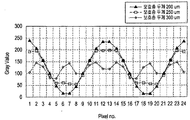
- FIG. 14 is a graph showing the gray value calculated based on the operational performance test results of a conventional capacitive fingerprint recognition sensor.
- first may be referred to as a second component
- second component may also be referred to as a first component.
- " and / or " includes any combination of a plurality of related listed items or any of a plurality of related listed items.
- the electronic device may be any device having a touch panel, and the electronic device may be referred to as a terminal, a mobile terminal, a mobile terminal, a communication terminal, a portable communication terminal, a portable mobile terminal, a display device and the like.
- the electronic device can be a smart phone, a mobile phone, a navigation device, a game machine, a TV, a head unit for a car, a notebook computer, a laptop computer, a tablet computer, a Personal Media Player (PMP) have.
- the electronic device may be implemented as a pocket-sized portable communication terminal having a wireless communication function.
- the electronic device may be a flexible device or a flexible display device.
- the electronic device can communicate with an external electronic device such as a server, or can perform an operation through interlocking with an external electronic device.
- the electronic device can transmit the image captured by the camera and / or the position information detected by the sensor unit to the server via the network.
- the network may include, but is not limited to, a mobile or cellular network, a local area network (LAN), a wireless local area network (WLAN), a wide area network (WAN) (SAN) or the like.
- FIG. 1 is a block diagram illustrating an electronic device 101 in a network environment 100, in accordance with various embodiments of the present invention.
- an electronic device 101 in a network environment 100 communicates with an electronic device 102 via a first network 198 (e.g., near-field wireless communication) or a second network 199 (E. G., Remote wireless communication).
- a first network 198 e.g., near-field wireless communication
- a second network 199 E. G., Remote wireless communication
- the electronic device 101 is capable of communicating with the electronic device 104 through the server 108.
- the electronic device 101 includes a processor 120, a memory 130, an input device 150, an audio output device 155, a display device 160, an audio module 170, a sensor module 176, an interface 177, a haptic module 179, a camera module 180, a power management module 188, a battery 189, a communication module 190, a subscriber identity module 196 and an antenna module 197, . ≪ / RTI >
- at least one (e.g., display 160 or camera module 180) of these components may be omitted from the electronic device 101, or other components may be added.
- some components such as, for example, a sensor module 176 (e.g., a fingerprint sensor, an iris sensor, or an illuminance sensor) embedded in a display device 160 Can be integrated.
- Processor 120 drives at least one other component (e.g., hardware or software component) of electronic device 101 that is coupled to processor 120 by driving software, e.g., program 140, And can perform various data processing and arithmetic operations.
- Processor 120 loads and processes commands or data received from other components (e.g., sensor module 176 or communication module 190) into volatile memory 132 and processes the resulting data into nonvolatile memory 134.
- the processor 120 may include a main processor 121 (e.g., a central processing unit or an application processor) and a coprocessor 123 operating independently thereof.
- the auxiliary processor 123 may additionally or alternatively use a lower power than the main processor 121 or may be coupled to a co-processor 123 (e.g., a graphics processor, an image signal processor, a sensor hub processor, ).
- a co-processor 123 e.g., a graphics processor, an image signal processor, a sensor hub processor, .
- the coprocessor 123 may be operated separately from or embedded in the main processor 121.
- the coprocessor 123 may be used in place of the main processor 121, for example, while the main processor 121 is in an inactive (e.g., sleep) state, At least one component (e.g., display 160, sensor module 176, or communications module 176) of the components of electronic device 101 (e.g., 190) associated with the function or states.
- the coprocessor 123 e.g., an image signal processor or communications processor
- the coprocessor 123 is implemented as a component of some other functionally related component (e.g., camera module 180 or communication module 190) .
- Memory 130 may store various data used by at least one component (e.g., processor 120 or sensor module 176) of electronic device 101, e.g., software (e.g., program 140) ), And input data or output data associated with the associated command.
- the memory 130 may include a volatile memory 132 or a non-volatile memory 134.
- the program 140 may be software stored in the memory 130 and may include, for example, an operating system 142, a middleware 144,
- the input device 150 is an apparatus for receiving a command or data to be used for a component (e.g., processor 120) of the electronic device 101 from the outside (e.g., a user) of the electronic device 101,
- a component e.g., processor 120
- a microphone, a mouse, or a keyboard may be included.
- the sound output device 155 is a device for outputting a sound signal to the outside of the electronic device 101.
- the sound output device 155 may be a speaker for general use such as a multimedia reproduction or a sound reproduction, .
- the receiver may be formed integrally or separately with the speaker.
- Display device 160 may be an apparatus for visually providing information to a user of electronic device 101 and may include, for example, a display, a hologram device or a projector and control circuitry for controlling the device. According to one embodiment, the display device 160 may include a touch sensor or a pressure sensor capable of measuring the intensity of the pressure on the touch.
- the audio module 170 is capable of bi-directionally converting sound and electrical signals. According to one embodiment, the audio module 170 may acquire sound through the input device 150, or may be coupled to an external output device 155, such as an electronic output device 155 or an external electronic device The device 102 (e.g., a speaker or headphone)).
- an external output device 155 such as an electronic output device 155 or an external electronic device
- the device 102 e.g., a speaker or headphone
- the sensor module 176 may generate an electrical signal or data value corresponding to an internal operating state (e.g., power or temperature) of the electronic device 101, or an external environmental condition.
- the sensor module 176 may be, for example, a gesture sensor, a gyro sensor, an air pressure sensor, a magnetic sensor, an acceleration sensor, a grip sensor, a proximity sensor, a color sensor, an infrared sensor, And a light intensity sensor.
- the interface 177 may support a designated protocol that may be wired or wirelessly connected to an external electronic device (e.g., the electronic device 102).
- the interface 177 may include a high definition multimedia interface (HDMI), a universal serial bus (USB) interface, an SD card interface, or an audio interface.
- HDMI high definition multimedia interface
- USB universal serial bus
- SD card interface Secure Digital interface
- audio interface an audio interface
- the connection terminal 178 may be a connector such as an HDMI connector, a USB connector, an SD card connector, or an audio connector that can physically connect the electronic device 101 and an external electronic device (e.g., the electronic device 102) (E.g., a headphone connector).
- an HDMI connector such as an HDMI connector, a USB connector, an SD card connector, or an audio connector that can physically connect the electronic device 101 and an external electronic device (e.g., the electronic device 102) (E.g., a headphone connector).
- the haptic module 179 may convert electrical signals into mechanical stimuli (e.g., vibrations or movements) or electrical stimuli that the user may perceive through tactile or kinesthetic sensations.
- the haptic module 179 may include, for example, a motor, a piezoelectric element, or an electrical stimulation device.
- the camera module 180 can capture a still image and a moving image.
- the camera module 180 may include one or more lenses, an image sensor, an image signal processor, or a flash.
- the power management module 188 is a module for managing the power supplied to the electronic device 101, and may be configured as at least a part of, for example, a power management integrated circuit (PMIC).
- PMIC power management integrated circuit
- the battery 189 is an apparatus for supplying power to at least one component of the electronic device 101 and may include, for example, a non-rechargeable primary battery, a rechargeable secondary battery, or a fuel cell.
- the communication module 190 is used to establish a wired or wireless communication channel between the electronic device 101 and an external electronic device (e.g., electronic device 102, electronic device 104, or server 108) And the like.
- Communication module 190 may include one or more communication processors that support wired communication or wireless communication, operating independently of processor 120 (e.g., an application processor).
- communication module 190 may include a wireless communication module 192 (e.g., a cellular communication module, a short range wireless communication module or a global navigation satellite system (GNSS) communication module, etc.) or a wired communication module 194 (E.g., a local area network (LAN) communication module or a power line communication module), and the corresponding communication module may be used to communicate with a first network 198 (e.g., Bluetooth, WiFi direct or IrDA Communication network) or a second network 199 (e.g., a telecommunications network such as a cellular network, the Internet or a computer network (e.g., a LAN or WAN)).
- the various types of communication modules 190 described above may be implemented as one chip integrated with at least some modules or as separate chips.
- the wireless communication module 192 may use the user information stored in the subscriber identification module 196 to identify and authenticate the electronic device 101 within the communication network.
- the antenna module 197 may include one or more antennas for externally transmitting or receiving signals or power.
- the communication module 190 e.g., the wireless communication module 192 may transmit or receive signals to or from an external electronic device via an antenna suitable for the communication scheme.
- FIG. 2 is an exploded perspective view showing an electronic device 200 including a fingerprint recognition sensor 204 according to one of various embodiments of the present invention.
- 3 is a perspective view illustrating an electronic device 200 including a fingerprint recognition sensor 204 in accordance with one of various embodiments of the present invention.
- an electronic device 200 may include a fingerprint sensor 204
- the fingerprint recognition sensor 204 may be embedded in the display panel 202b or may be disposed in a stacked structure with the display panel 202b.
- the fingerprint recognition sensor 204 may include pixels (or a pixel array of pixels) that form a capacitance corresponding to at least a portion of a subject (e.g., a user fingerprint).
- a processor e.g., processor 120 of FIG. 1
- the electronic device 200 may generate a subject image (e.g., a fingerprint image) based on the capacitance formed by each of the pixels .
- the electronic device 200 may include a housing 201 and a display device 202 (e.g., the display device 160 of FIG. 1), and the housing 201 may include at least one
- a main circuit board 231 and / or an auxiliary circuit board 233, a battery 235 (e.g., the battery 189 in Fig. 1), and the like can be accommodated.
- the various modules and / or devices of FIG. 1 may be mounted on the main circuit board 231 or the like in the form of integrated circuit chips or electrical components.
- the housing 201 may include a housing member 201a and a cover plate 201b and may include a first surface (e.g., a front surface) facing the first direction D1 A second surface (e.g., a back surface) facing a second direction D2 opposite the direction D1, and a sidewall formed at least partially surrounding the space between the first surface and the second surface.
- the housing member 201a defines a space for accommodating the circuit board (e.g., the main circuit board 231 and / or the auxiliary circuit board 233), and the cover plate 201b May be coupled to the housing member 201a to form a second surface of the housing 201.
- the first side of the housing 201 may be at least partially open, and the display device 202 may engage to close the first side of the housing 201.
- the appearance of the electronic device 200 may be substantially completed by coupling the display device 202 to the housing 201.
- the cover plate 201b can be molded and manufactured substantially integrally with the housing member 201a.
- the housing 201 may have a uni-body structure.
- the cover plate 201b may include at least one opening 211 (s).
- the term " opening " may mean, for example, a through hole formed to penetrate from the inner side to the outer side of the cover plate 201b, It may be a transparent portion that optically / visually transmits light but does not connect the inner space and the outer space of the cover plate 201b.
- the fingerprint recognition sensor 204 may be disposed on the cover plate 201b, for example, corresponding to the opening 211. [ The arrangement of the fingerprint recognition sensor 204 will be described in more detail with reference to FIG.
- the display device 202 may include the display panel 202b and a window member 202a that protects the display panel 202b.
- the window member 202a may be mounted on the first surface of the housing 201 to form a part of the appearance of the electronic device 200.
- the pixel array e.g., the pixel array 411 of FIG. 4
- the pixel array may be formed on the semiconductor device 401 or may be formed on the transparent electrode using a conductor such as indium- And the pixel array may be embedded in the display panel 202b or stacked with the display panel 202b.
- the structure of the fingerprint sensor 204, such as a pixel array, will be described in more detail with reference to FIG.
- FIG. 4 is a block diagram illustrating a fingerprint recognition sensor 400 according to various embodiments of the present invention.
- the fingerprint recognition sensor 400 (e.g., the fingerprint recognition sensor 204 of FIG. 2) includes a pixel array 411, a passivation layer 402, a guide wall 421) < / RTI >
- the pixel array 411 includes sensors (e.g., pixels 413 in FIG. 5) that each form a capacitance corresponding to at least a portion of a subject (e.g., a user finger or fingerprint) ). ≪ / RTI >
- a sensor layer for example, the pixel array 411
- the present invention is not limited to this, and as mentioned above, an electrode array composed of an array of transparent electrodes can replace the pixel array 411.
- the semiconductor device 401 may not be disposed.
- the semiconductor device 401 may be mounted on a circuit board (e.g., the auxiliary circuit board 233 in FIG. 2) of the above-described electronic device (e.g., the electronic device 200 of FIG. 2).
- the semiconductor device 401 may be connected to a circuit pattern of the circuit board 409 through wire bonding or the like to receive a power supply and a control signal or to transmit data regarding the detected capacitance.
- the passivation layer 402 may include a dielectric layer that provides a stable operating environment for the pixel array 411 while preventing the pixel array 411 from being directly exposed to the external environment .
- the protection layer 402 protects the pixel array 411 from the external environment while blocking the electromagnetic effect in forming the electrostatic capacitance, or may reduce the sensitivity (e.g., recognition distance) of the fingerprint recognition sensor 400 Can be improved.
- the protective layer 402 may include a molding layer 402a (hereinafter, referred to as a 'molding layer').
- the molding layer 402a is formed to cover the semiconductor device 401 on the circuit board 409 by applying an epoxy or the like to the semiconductor device 401.
- the molding layer 402a can prevent the semiconductor device 401 or the like from being directly exposed to the external environment, thereby preventing contamination or damage due to foreign matter.
- the molding layer 402a is made of a high- (For example, recognition distance) in fingerprint recognition by improving the signal-to-noise ratio (SNR) and the like of the fingerprint sensor 400.
- SNR signal-to-noise ratio
- the protective layer 402 may include an adhesive layer 402b and / or a cover member 402c.
- the adhesive layer 402b may be formed on the surface of the molding layer 402a to bond the cover member 402c to the molding layer 402a.
- the adhesive layer 402b may comprise an optical adhesive, a thermosetting adhesive, a pressure sensitive adhesive, and may be formed by applying such an adhesive to the surface of the molding layer 402a, : The base film 425a in Fig. 8).
- the cover member 402c may be bonded to the molding layer 402a, for example, and may substantially form the surface of the fingerprint recognition sensor 400.
- the cover member 402c may be made of a material having a surface hardness of 9H or higher, such as tempered glass.
- tempered glass is shown as an example of the cover member 402c, but the present invention is not limited thereto.
- the cover member 402c is a material that sufficiently provides surface hardness, (For example, a dielectric constant of 7 or more) so that the pixels of the pixel array 411 can form capacitances corresponding to the user's body.
- the protective layer 402 may be made of a material having a certain permittivity and a thickness so that each pixel of the pixel array 411 can form a capacitance corresponding to a part of a user's body Environment can be created.
- the cover member 402c may be replaced by a window member (e.g., window member 202a of FIG. 2) or a cover plate (e.g., cover plate 201b of FIG. 2) of the electronic device.
- a window member e.g., window member 202a of FIG. 2
- a cover plate e.g., cover plate 201b of FIG. 2
- the fingerprint recognition sensor 400 is embedded or stacked on the display panel 202b, a part of the area of the window member 202a (for example, the area indicated by 'F' in FIG. 3) And can be utilized as a cover member of the fingerprint recognition sensor 400 (e.g., the fingerprint recognition sensor 204 in Fig. 2).
- the fingerprint recognition sensor 400 detects a user fingerprint or the like on the second surface of the electronic device 200
- a part of the cover plate 201b is utilized as a cover member of the fingerprint recognition sensor 400 .
- the fingerprint sensor 400 may be disposed on an opening (e.g., opening 211 in FIG. 2) of the cover plate 201b.
- the cover member 402c is attached to the electronic device 200 in a state of closing the opening 211 .
- the cover member 402c When a portion of the window member 202a or the cover plate 201b of the electronic device 200 is utilized as the cover member 402c, at least a portion utilized as the cover member 402c has a certain degree of surface hardness For example, 9H or more), and may have a certain degree of dielectric constant (for example, a dielectric constant of 7 or more).
- the dielectric layer for example, the protective layer 402 may include a first partial region P1 having a first dielectric constant and a second partial region P1 having a second dielectric constant different from the first dielectric constant, P2).
- the first partial area P1 is part of the cover member 402c and can be made of a glass material.
- the first partial area P1 may be formed by a part of the window member 202a of FIG.
- the second partial area P2 may mean an area where the guide wall 421 (s) is formed, and may be formed of an epoxy-based resin.
- the guide walls 421 may be arranged in the protective layer 402 at regular intervals.
- the guide walls 421 may include a hole or recessed portion formed at a predetermined interval from the inner surface of the cover member 402c, and the pixel arrays 411, They can be arranged along a parallel direction.
- the guide wall 421 may have a diaphragm shape that divides an area illuminated by the pixel array 411 into an area corresponding to each pixel or an area corresponding to a plurality of adjacent pixels.
- the guide walls 421 may be arranged to correspond to the width or length of each of the pixels, or may be arranged at an interval larger than the width or length of each of the pixels.
- the guide wall 421 has a groove shape formed inside the cover member 402c, but the present invention is not limited thereto.
- the guide walls 421 may be formed in the adhesive layer 402b and / or the molding layer 402a.
- Lt; / RTI > The formation positions of the guide walls 421 will be described in more detail with reference to FIGS. 5 to 8.
- FIG. 5 the protective layer 402
- the guide wall 421 may have a dielectric constant different from other portions of the protective layer 402.
- the guide wall 421 may have a lower dielectric constant than other portions of the protective layer 402.
- the groove portion formed on the inner surface of the cover member 402c may be filled with air to form a molding layer 402a or an adhesive 402b which forms another portion of the cover member 402c or a part of the protective layer 402, It can have a lower dielectric constant.
- some numerical values are given as high or low values with respect to the dielectric constant of the protective layer 402 and the dielectric constant of the guide wall 421, but the present invention is not limited thereto .
- the dielectric constant of the guide wall 421 may be set lower than the dielectric constant of the protective layer 402.
- the protective layer 402 includes a glass material having a dielectric constant of about 8
- the guide wall 421 formed in the protective layer 402 may include an epoxy resin having a dielectric constant of about 3.5.
- the guide wall 421 has a low dielectric constant, so that it is possible to reduce the distance between the pixel array 411 (e.g., pixels) and the user's body (e.g., fingerprint)
- the formation of the electrostatic capacitance can be suppressed.
- formation of a capacitance corresponding to a region outside the region of interest (ROI) of each pixel constituting the pixel array 411 can be suppressed.
- the fingerprint recognition sensor 400 may acquire a fingerprint image of sufficient resolution to detect a user fingerprint even at a distance of about 300 micrometers (m) from the surface of the pixel array 411.
- a fingerprint sensor of the structure without the guide wall 421 (s) under the same conditions of other structure / performance and the like is difficult to authenticate or identify the user through a fingerprint image obtained at a distance of approximately 250 micrometers ( ⁇ ) .
- the guide wall 421 can suppress the formation of parasitic capacitance, thereby improving the resolution of the fingerprint image, Can be improved. Therefore, in fabricating the fingerprint sensor 400, the thickness T of the protective layer 402 can be increased, and the thickness T of the protective layer 402, for example, the cover member 402c, It is possible to facilitate processing.
- FIG. 5 is a configuration diagram showing an example of forming a guide wall 421 of a fingerprint sensor according to various embodiments of the present invention.
- FIG. 6 is a plan view showing a projection of a fingerprint sensor according to various embodiments of the present invention when viewed from the outside of a protective layer.
- the sensor layer for example, the pixel array 411 may be comprised of a plurality of sensors, for example, an array of a plurality of pixels 413, And a third region R3 (s) formed between the first and second regions R1 and R2.
- the first region R1 and the second region R2 correspond to the first region R1 and the second region R1, respectively.
- the first partial region P1 having a first permittivity is disposed substantially over at least a partial region of the first or second region R1, R2, and the second permittivity
- the second partial region P2 may be disposed on the third region R3.
- a wiring electrically connected to each of the sensors, for example, the pixels 413 may be formed in the third region R3.
- the guide walls 421 are formed in the dielectric layer, for example, in the second partial area P2 corresponding to the third area R3 in the protective layer 402, (Hereinafter referred to as a " detection area ") of the array 411 can be divided into a plurality of areas.
- the guide walls 421 may divide the detection area into a region illuminated by each of the pixels 413, or may include an area illuminated by at least two neighboring pixels 413 among the pixels 413 It can be divided from other areas.
- each region divided by the guide walls 421 will be referred to as an ROI.
- the guide walls 421 may set the ROI to correspond to each of the pixels 413 or to a plurality of adjacent pixels 413.
- each of the pixels 413 forms a capacitance corresponding to the object in the region of interest (ROI), for example, in a region surrounded by the guide walls 421 disposed around the ROI can do.
- ROI region of interest
- the guide walls 421 may be formed of a groove or a low dielectric constant material filled with a low dielectric constant material (e.g., air).
- the guide walls 421 can suppress the formation of electrostatic capacitance between two objects (for example, a part of the pixel 413 and a part of the object corresponding thereto).
- the guide walls 421 may be disposed on an area of the pixel array 411 that does not overlap with the pixels 413.
- the guide walls 421 may be disposed between the pixels 413 to facilitate the formation of capacitances in the ROI of each of the pixels 413, It is possible to suppress formation of parasitic capacitance in the region.
- the widths L1 and L2 of the pixels 413 may be made to be 50 micrometers, respectively, and may be arranged adjacent to other pixels at intervals of 10 micrometers (G) have.
- the guide walls 421 may have a thickness corresponding to the gap G between the pixels 413 and may extend along the width L1 or the length L2 of the pixels 413, .
- the guide walls 421 (s) extending along the width L1 or length L2 of the pixels 413 may extend approximately 30 micrometers long (L3, L4).
- the lengths L3 and L4 of the guide wall 421 (s) are illustrated as approximately 30 micrometers, but the present invention is not limited thereto.
- the guide wall 421 (s) correspond to the entire width (L1) or length (L2) of the pixels 413, or to the entire length of the row or column in which the pixels 413 are arranged Lt; / RTI >
- FIG. 7 is a perspective view illustrating a molding layer 402a of a fingerprint sensor according to various embodiments of the present invention.
- the guide wall 421 may include a groove 423 formed in the molding layer 402a.
- the groove portion 423 may include, for example, slit (s) formed on the surface of the molding layer 402a, and the slit (s) may be filled with a low dielectric constant material .
- the slits (s) may be connected to one another and have a lattice pattern.
- the slits may be formed in the cover member 402c and / or in the adhesive layer 402b corresponding to the guide wall of the adhesive layer 402b Can be extended / arranged along the locus.
- FIG. 8 is a perspective view illustrating an adhesive layer 402b of a fingerprint sensor according to various embodiments of the present invention.
- the adhesive layer 402b may include a base film 425a, a through hole 425b, and an adhesive 425c.
- the adhesive layer 402b may have a tape shape including the adhesive 425c applied to at least one side of the base film 425a.
- the through holes 425b may be formed to penetrate the base film 425a and may be filled with a low dielectric constant material, for example, air to provide the function of the guide wall described above.
- a part of the adhesive 425c may be filled in the through hole 425b.
- the adhesive 425c may be evenly distributed throughout the bonding region.
- a part of the base film may provide the function of the guide wall described above.
- the adhesive is evenly distributed throughout the bonding region between the base film and the molding layer 402a (or between the base film and the cover member 402c), if the dielectric constant is lower than that of the base film, .
- the adhesive may have a higher dielectric constant than the base film, and the through- May be formed corresponding to the region of interest (e.g., ROI of FIG. 6).
- a through-hole formed in the base film is filled with an adhesive while being formed corresponding to the region of interest (ROI), and at least a part of the base film having a lower dielectric constant than the adhesive can provide the function of the guide wall described above.
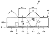
- FIG. 9 is a block diagram illustrating the operation of the fingerprint recognition sensor 500 according to various embodiments of the present invention.
- the fingerprint recognition sensor 500 (e.g., the fingerprint sensor 204, 400 of FIG. 2 or 4) includes a pixel array 511 (e.g., A pixel array 411 of FIG. 5), a protective layer 502 disposed on the pixel array 511, and guide walls 521 formed in the protective layer 502.
- the guide walls 521 may be disposed between at least two adjacent pixels 513,
- the pixels 513 may form electrostatic capacitances Cr and Cv corresponding to at least a part of the subject in a region surrounded by the guide walls 521 disposed around the pixels 513.
- 'FP' may refer to the fingerprint curve of the user, 'R' to the rigid portion of the user fingerprint, and 'V' to the valley portion of the user fingerprint.
- each of the guide walls 521 may be filled with a material having a lower dielectric constant than the other portions of the protective layer 502, or may be formed of a low dielectric constant material.
- the capacitance formed between two objects or electrodes e.g., the pixel 513 (s) and the corresponding portion of the subject
- the capacitance formed between two objects or electrodes is inversely proportional to the distance between the two objects and is dependent on the dielectric constant of the material (s) It can be proportional.
- Each of the guide walls 521 has a low dielectric constant (e.g., a dielectric constant of 2 or less), and is disposed between the pixels 513, thereby generating parasitic static electricity corresponding to a subject portion of an area outside the ROI The formation of the capacitance Cf can be suppressed.
- the difference between the capacitances Cr and Cv formed corresponding to the ridge R and the valley line V of the fingerprint curve FP can be made clearer .
- the difference between the capacitances Cr and Cv formed corresponding to the ridge R and the bone line V becomes more clear so that the pixel arrays 511 and / The resolution of the obtained fingerprint image can be increased.
- a processor e.g., processor 120 of Figure 1 or an image signal processor included therein
- an electronic device e.g., electronic device 101, 102, 104, 200 of Figure 1 or Figure 2
- Cr, Cv of the user's fingerprint image.
- FIG. 10 is a cross-sectional view illustrating an electronic device 600 including a fingerprint recognition sensor 603 according to another of the various embodiments of the present invention.
- the fingerprint recognition sensor 204 is illustrated as a separate component from the display device 202, e.g., the display panel 202b, but, as mentioned above,
- the fingerprint recognition sensor according to the embodiment may be embedded or laminated on a display device or a display panel.
- the electronic device 600 may include a window member 602a and a display panel 602b, and a fingerprint recognition sensor 603 embedded or layered on a display device or a display panel 602b .
- the display panel 602b may include a light emitting layer 621, a polarizing plate 623, and a touch screen panel 625.
- the light emitting layer 621 may be enclosed between substrates (not shown) bonded to each other.
- the touch screen panel 623 may be incorporated into the window member 602a.
- the display panel 602b may be attached to the inner surface of the window member 602a through an adhesive layer 629, for example, a pressure sensitive adhesive or an optical clear adhesive.
- the fingerprint sensor 603 may include a pixel array 631 disposed on the polarizer 623 and / or on the same layer as the touch screen panel 625, and a protective layer 633 .
- the protective layer 633 may include a part of the adhesive layer 629 and / or a part of the window member 602a.
- the adhesive layer 402b may be formed by a part of the adhesive layer 629.
- the cover member 402c may be formed by a portion of the window member 602a.
- a molding layer 402a may be formed on the same layer as the touch screen panel 625 with the pixel array 631 in the protective layer 402 of FIG.
- the molding layer 402a may be formed by another portion of the adhesive layer 629. For example, if the pixel array 631 is formed on the same layer as the display panel 602b, such as the touch screen panel 625, the molding layer 402a may be removed or removed.
- the fingerprint sensor 603 may include a guide wall 635 (s) (e.g., the guide wall 421 of FIG. 4) having a dielectric constant different from that of the passivation layer 633 have.
- the guide walls 635 may be disposed between the pixel array 631 and a subject (e.g., a user fingerprint), and correspond to regions outside the region of interest of each pixel constituting the pixel array 631 It is possible to suppress the formation of the electrostatic capacitance.
- the number and spacing of the guide walls 635 can be variously set in consideration of the use environment of the fingerprint recognition sensor 603 and the like.
- the electronic device 600 may include a flexible printed circuit board 641 extending from the display panel 602b and / or the fingerprint recognition sensor 603.
- the display panel 602b and / or the fingerprint recognition sensor 603 may be connected to the main circuit board (e.g., the main circuit board 231 in Fig. 2) via the flexible printed circuit board 641, The integrated circuit chip 643 provided on the flexible printed circuit board 641, and the like.
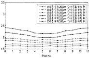
- FIG. 11 is a graph showing operational test results of a fingerprint recognition sensor according to various embodiments of the present invention.
- the graph shown in Fig. 11 shows that the interval of ridges (e.g., the ridges R in Fig. 9) of the user fingerprint (or the interval of the ridges (e.g., the ridges V in Fig. 9) ,
- the electrostatic capacity formed in each pixel is measured according to the recognition distance (for example, the protective layer thickness T in FIG. 4), and the measurement is performed before and after the above-described formation of the guide wall.
- Pixel numbers described in the horizontal axis in the graph of Fig. 11 are numbers sequentially assigned to the pixels constituting one row or column of the pixel array (e.g., selected in the pixel array 411 of Fig. 5).
- pixels corresponding to the ridge portion R of the user fingerprint denote pixels corresponding to the ridge portion R of the user fingerprint and pixel numbers 3 to 8 denote pixels corresponding to the fingerprint portion V of the user fingerprint, And the pixel corresponding to the ridge portion or the bone line portion may be different depending on the measurement time point.
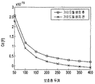
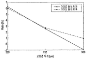
- FIG. 12 and FIG. 13 are graphs comparing capacitance measurement values according to recognition distances of a fingerprint recognition sensor according to various embodiments of the present invention.
- 'Cd' is a difference (hereinafter referred to as a difference (hereinafter referred to as a difference) between the measured value of the capacitance (Cr) corresponding to the ridge R and the measured value of the capacitance Cv corresponding to the bone-
- the difference value Cd of the fingerprint recognition sensor including the guide wall 521 is about 0.3 to about 0.3 times the fingerprint recognition sensor that does not include the fingerprint sensor at a measurement distance in the range of 100 to 400 micrometers. 0.4 fF.
- a fingerprint sensor (e.g., the fingerprint sensor 500 of FIG. 9) according to various embodiments of the present invention includes a guide wall to further improve the difference value Cd of such capacitance.
- the fingerprint sensor according to various embodiments of the present invention includes a guide wall, thereby reducing a load due to signal processing for acquiring a fingerprint image.
- the fingerprint recognition sensor when the measurement distance, for example, the thickness T of the protective layers 402 and 502 in Figs. 4 or 9 reaches approximately 300 micrometers, a conventional fingerprint recognition sensor
- the difference value Cd in the fingerprint recognition sensor in which a guide wall is not disposed is substantially zero.
- the electrostatic capacity corresponding to the ridge portion measured by the conventional fingerprint recognition sensor is substantially equal to the electrostatic capacitance corresponding to the ridge portion, Can not be distinguished.
- the fingerprint recognition sensor according to various embodiments of the present invention can have a positive difference value (Cd) even if the measurement distance exceeds 300 micrometers, A fingerprint image can be obtained.
- 'Ratio' represents the ratio of the difference value Cd (hereinafter referred to as a 'ratio value') to the electrostatic capacity formed corresponding to the ridge R, (Ration) can have a tendency to decrease gradually as the measurement distance increases.
- the ratio value (Ratio) in a typical fingerprint recognition sensor for example, a fingerprint recognition sensor in which the guide wall is not disposed as described above
- the capacitance measurement value formed corresponding to the ridge portion may be lower than the capacitance measurement value formed corresponding to the bone line portion.
- a fingerprint recognition sensor e.g., the fingerprint recognition sensor 500 of FIG. 9 according to various embodiments of the present invention maintains a ratio value of about 1% even if the measurement distance reaches 300 micrometers Thus obtaining a fingerprint image having a resolution required for user authentication (or identification) and the like.
- FIG. 14 is a graph showing the gray value calculated based on the operational performance test results of a conventional capacitive fingerprint recognition sensor.
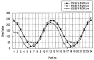
- 15 is a graph showing gray values calculated on the basis of operational test results of a fingerprint recognition sensor according to various embodiments of the present invention.
- 14 and 15 are graphs showing a gray value of a fingerprint image obtained after acquiring a fingerprint image based on the electrostatic capacity formed by each pixel of the fingerprint recognition sensor, The measurement results can be compared according to the thickness.
- a fingerprint sensor of a conventional capacitance type can acquire a fingerprint image with good resolution at a measurement distance of 200 to 250 micrometers, but at a measurement distance of 300 micrometers, And the bone marrow may be difficult to distinguish.
- the fingerprint sensor according to various embodiments of the present invention can acquire a fingerprint image with a good resolution even at a measurement distance of 300 micrometers while operating in a capacitive manner.
- the fingerprint recognition sensor according to various embodiments of the present invention can improve the recognition distance, it is possible to obtain a good fingerprint image even if the thickness of the protection layer is secured.
- the cover member 402c of FIG. 4 is made of tempered glass, it is possible to provide an environment in which the thickness of the tempered glass can be made thicker.
- the cover member of a conventional fingerprint sensor is made of 150 micrometer thick tempered glass, then the cover member of the fingerprint sensor according to various embodiments of the present invention may be 200 And can be made of tempered glass having a thickness of more than micrometers. Therefore, the fingerprint sensor according to the various embodiments of the present invention can reduce manufacturing cost and time, for example, cost and time required for processing the cover member.
- an electronic device includes:
- a pixel array comprising an array of pixels each forming a capacitance corresponding to at least a portion of a subject
- And may include guide walls formed and arranged in the protective layer,
- the guide walls may have a lower dielectric constant than other portions of the protective layer and may be arranged at an interval corresponding to at least the width or length of each of the pixels.
- each of the pixels when projecting the protective layer from the outer surface of the protective layer, each of the pixels forms a capacitance corresponding to the object in the area surrounded by the guide walls disposed therearound .
- the guide walls when the protective layer is projected on the outer surface of the protective layer, the guide walls may be disposed between at least two adjacent pixels.
- such an electronic device may further include a semiconductor device mounted on a circuit board and including the pixel array,
- the protective layer may include a molding layer formed on the circuit board so as to surround the semiconductor device.
- the guide wall may include a hole or recessed portion formed in the surface of the molding layer
- the groove portion may be filled with a low dielectric constant material.
- such an electronic device may further include a semiconductor device mounted on a circuit board, the semiconductor device including the pixel array,
- the protection layer may include a cover member mounted on the semiconductor device,
- the guide wall may include a groove formed on an inner surface of the cover member and filled with a low dielectric constant material.
- such an electronic device may further include a semiconductor device mounted on a circuit board, the semiconductor device including the pixel array,
- the protective layer may be formed,
- the guide wall may be formed in at least one of the molding layer, the adhesive layer, or the cover member.
- a sensor layer including a first sensor and a second sensor for sensing capacitance with respect to at least a portion of an external subject that may contact the electronic device, A second region in which the second sensor is disposed, and a third region formed between the first region and the second region;
- a second portion disposed over and over at least a portion of the first region and the second region and having a first permittivity and a second portion disposed over the third region and having a second permittivity, And a dielectric layer comprising regions.
- the second partial regions have a lower dielectric constant than the other portions of the dielectric layer, and may be arranged at least at intervals corresponding to the width or length of the first sensor or the second sensor.
- the second partial regions may be disposed between the first sensor and the second sensor when projecting the dielectric layer at the outer surface of the dielectric layer.
- such an electronic device comprises:
- the sensor layer may be disposed inside the display device.
- the dielectric layer may be formed to include a part of the window member.
- such an electronic device comprises:
- the sensor layer may be disposed on the opening.
- such an electronic device comprises:
- the sensor layer may be formed by at least a portion of the semiconductor device
- such an electronic device comprises:
- the cover member is mounted so as to close the opening, and the sensor layer can be mounted in the housing.
- the guide wall may be formed in at least one of the molding layer, the adhesive layer, or the cover member.
- such an electronic device may further comprise a processor
- the processor may generate an image of an external subject contacted with the electronic device based on the capacitance formed by the first sensor or the second sensors.
Landscapes
- Engineering & Computer Science (AREA)
- Theoretical Computer Science (AREA)
- Human Computer Interaction (AREA)
- Physics & Mathematics (AREA)
- General Physics & Mathematics (AREA)
- General Engineering & Computer Science (AREA)
- Multimedia (AREA)
- Image Input (AREA)
- Measurement Of Length, Angles, Or The Like Using Electric Or Magnetic Means (AREA)
- Measurement Of The Respiration, Hearing Ability, Form, And Blood Characteristics Of Living Organisms (AREA)
Abstract
본 발명의 다양한 실시예에 따르면, 전자 장치는, 피사체의 적어도 일부분에 대응하여 정전용량을 각각 형성하는 픽셀들의 배열로 이루어진 픽셀 어레이; 상기 픽셀 어레이 상에 배치된 보호층; 및 상기 보호층 내에 형성, 배열된 가이드 월(guide wall)들을 포함할 수 있으며, 상기 가이드 월들은 상기 보호층의 다른 부분보다 낮은 유전율을 가지며, 적어도 상기 픽셀들 각각의 폭 또는 길이에 대응하는 간격으로 배열될 수 있다. 상기와 같은 전자 장치는 실시예에 따라 다양할 수 있다.
Description
본 발명의 다양한 실시예는 전자 장치에 관한 것으로서, 예를 들면, 사용자의 생체 정보 검출을 위한 센서 및 그를 포함하는 전자 장치에 관한 것이다.
통상적으로 전자 장치라 함은, 가전제품으로부터, 전자 수첩, 휴대용 멀티미디어 재생기, 이동통신 단말기, 태블릿 PC, 영상/음향 장치, 데스크톱/랩톱 컴퓨터, 차량용 내비게이션 등, 탑재된 프로그램에 따라 특정 기능을 수행하는 장치를 의미한다. 예를 들면, 이러한 전자 장치들은 저장된 정보를 음향이나 영상으로 출력할 수 있다. 전자 장치의 집적도가 높아지고, 초고속, 대용량 무선통신이 보편화되면서, 최근에는, 이동통신 단말기 하나에 다양한 기능이 탑재되고 있다. 예를 들면, 통신 기능뿐만 아니라, 게임과 같은 엔터테인먼트 기능, 음악/동영상 재생과 같은 멀티미디어 기능, 모바일 뱅킹 등을 위한 통신 및 보안 기능, 일정 관리나 전자 지갑 등의 기능이 하나의 전자 장치에 집약되고 있는 것이다.
최근에는, 전자 장치 자체에 저장된 개인정보 보호 기능뿐만 아니라, 모바일 뱅킹, 모바일 신용 카드, 전자 지갑 등을 실행하는데 필요한 보안 기능이 전자 장치, 예를 들면, 이통통신 단말기와 같은 휴대용 전자 장치에 탑재되고 있다. 전자 장치에 탑재된 보안 기능으로는 사용자 설정에 따른 비밀번호나 잠금 패턴, 보안 업체를 매개로 하는 사용자 인증 등을 예로 들 수 있다. 비밀번호나 보안 업체를 매개로 하는 인증 방식은, 비밀번호의 유출 가능성이 높아 보안 수준이 낮거나, 보안 업체를 매개로 하는 번거로움이 있을 수 있다. 이에 대한 대안으로, 생체 인증 방식, 예를 들면, 지문이나 홍채 인식을 이용한 사용자 인증 방식은 상당한 보안 수준을 확보하면서 사용 편의성을 높일 수 있다.
지문 인식을 통한 사용자 인증 방식에는, 광학 구조를 이용한 방식 또는 초음파 방식 등이 있다. 이는 조명 또는 초음파를 사용자 지문에 조사하여 사용자 지문에서 반사된 조명이나 초음파로부터 사용자의 지문 이미지를 검출하는 방식이다. 다른 형태로, 다수의 센서, 전극 또는 픽셀들의 배열로 이루어진 픽셀 어레이를 이용한 정전용량 방식의 지문 인식 센서가 제안될 수 있다. 정전용량 방식의 지문 인식 센서에서, 전극 또는 픽셀들은 피사체, 예를 들면, 사용자 지문의 적어도 일부(예: 융선부(ridge portion) 또는 골선부(valley portion))에 대응하여 정전용량을 형성할 수 있다. 이러한 정전용량은 사용자 지문 이미지를 생성하기 위한 기초 데이터를 제공할 수 있다. 이러한 정전용량 방식의 지문 인식 센서는, 발광 소자 또는 초음파 발진기 등을 탑재한 지문 인식 센서(광학 구조 또는 초음파 방식의 센서)보다 그 구조가 간결해질 수 있다.
이러한 정전용량 방식의 지문 인식 센서를 구현함에 있어, 정전용량을 형성하는 전극 또는 픽셀의 안정된 작동 환경을 제공하기 위한 보호층(passivation layer)이 제공될 수 있다. 이러한 보호층을 형성함에 있어 전극 또는 픽셀이 정전용량을 형성할 수 있는 적절한 거리(예: 인식 거리)를 확보하기 위해 픽셀 어레이 상에서의 보호층 두께에 제한이 있을 수 있다.
어떤 실시예에서, 지문 인식 센서는 사용자 신체 일부(예: 손가락)와의 접촉을 통해 지문 이미지를 검출할 수 있다. 예컨대, 지문 인식 센서의 표면(예: 보호층의 표면)은 실질적으로 외부 환경에 노출될 수 있으며, 사용자 신체 일부를 포함하는 외부 물체와 마찰할 수 있다. 따라서 지문 인식 센서의 표면에서 긁힘 등의 손상이 발생될 수 있으며, 손상된 센서 표면으로 인해 지문 등의 인식률이 저하될 수 있다.
센서 표면의 손상은, 경도가 높은 재질, 예를 들면, 강화유리 필름 등을 보호층, 예를 들어, 센서 표면에 배치하여 방지할 수 있다. 하지만, 보호층에 배치하기 위한 강화유리 필름 등은 가공에 있어 비용과 시간이 소요되면서도 수율이 낮을 수 있다. 더욱이, 적절한 인식 거리 확보를 위해 보호층의 두께에 제한이 있는 현실에서, 이러한 가공 비용이나 시간은 더욱 증가될 수 있다.
어떤 실시예에서, 정전방식 지문센서는 디스플레이 영역(디스플레이 패널 내부 or 패널 상부)에 위치할 수 있다. 디스플레이 영역에 지문센서가 위치할 경우 사용성이 향상될 수 있는 장점이 있으나 디스플레이 윈도우, 편광판, 터치스크린 패널, 접착층 등과 같은 여러 층 통과해서 지문 이미지를 취득해야 하는데 이러한 적층구조는 인식 거리를 증가시켜 지문 이미지의 품질을 심각하게 저하시킬 수 있다.
본 발명의 다양한 실시예는, 정전용량을 방식의 지문 인식 센서 및 그를 포함하는 전자 장치를 제공할 수 있다.
본 발명의 다양한 실시예는, 피사체의 적어도 일부에 대응하여 정전용량을 형성함에 있어, 향상된 인식 거리를 가지는 지문 인식 센서 및 그를 포함하는 전자 장치를 제공할 수 있다.
본 발명의 다양한 실시예에 따르면, 전자 장치는,
피사체의 적어도 일부분에 대응하여 정전용량을 각각 형성하는 픽셀들의 배열로 이루어진 픽셀 어레이;
상기 픽셀 어레이 상에 배치된 보호층; 및
상기 보호층 내에 형성, 배열된 가이드 월(guide wall)들을 포함할 수 있으며,
상기 가이드 월들은 상기 보호층의 다른 부분보다 낮은 유전율을 가지며, 적어도 상기 픽셀들 각각의 폭 또는 길이에 대응하는 간격으로 배열될 수 있다.
본 발명의 다양한 실시예에 따른 전자 장치는,
상기 전자 장치에 접촉될 수 있는 외부 피사체의 적어도 일부분에 대한 정전용량을 감지하기 위한 제1 센서 및 제2 센서를 포함하는 센서층을 포함하고, 상기 센서층은 상기 제1 센서가 배치된 제1 영역, 상기 제2 센서가 배치된 제2 영역 및 상기 제1 영역과 상기 제2 영역 사이에 형성된 제3 영역을 포함할 수 있고; 및
상기 제1 영역 및 상기 제2 영역의 적어도 일부 영역 상(over)에 배치되고 제1 유전율을 가지는 제1 부분 영역들 및 상기 제3 영역 상(over)에 배치되고 제2 유전율을 가지는 제2 부분 영역들을 포함하는 유전층을 포함할 수 있다.
본 발명의 다양한 실시예에 따른 지문 인식 센서(및/또는 그를 포함하는 전자 장치)는 픽셀 어레이 상에 배치된 보호층 내에 가이드 월을 형성함으로써, 각 픽셀들의 관심 영역(region of interest; ROI)의 주변부에 대응하는 정전용량(예: 기생 정전용량)의 형성을 억제, 완화할 수 있다. 이를 통해 사용자 지문의 융선부와 골선부가 더욱 선명하게 구분된 지문 이미지를 획득할 수 있으며, 상기와 같은 가이드 월이 배치된 지문 인식 센서에서는, 가이드 월이 배치되지 않은 센서와 비교할 때, 더 먼 거리에 피사체가 위치하더라도 양호한 해상도의 지문 이미지를 획득할 수 있다. 예컨대, 상기와 같은 가이드 월은 지문 인식 센서(예: 픽셀 어레이)의 인식 거리를 향상시킬 수 있다.
본 발명의 다양한 실시예에 따르면, 정전용량 방식의 지문 인식 센서를 제작함에 있어, 지문 인식 센서의 인식 거리가 향상됨으로써, 보호층(예: 경도가 높은 강화유리 필름)의 두께 제한이 완화될 수 있다. 예컨대, 보호층 제작에 있어, 경도가 높은 소재를 가공하는 경우, 가공 비용이나 시간을 절감할 수 있으며, 동일한 가공 비용이나 시간이 소요되더라도 적어도 수율을 향상시킬 수 있다.
도 1은 본 발명의 다양한 실시예들에 따른, 네트워크 환경 내의 전자 장치를 나타내는 블럭도이다.
도 2는 본 발명의 다양한 실시예 중 하나에 따른 지문 인식 센서를 포함하는 전자 장치를 나타내는 분리 사시도이다.
도 3은 본 발명의 다양한 실시예 중 하나에 따른 지문 인식 센서를 포함하는 전자 장치를 나타내는 사시도이다.
도 4는 본 발명의 다양한 실시예에 따른 지문 인식 센서를 나타내는 구성도이다.
도 5는 본 발명의 다양한 실시예에 따른 지문 인식 센서의 가이드 월 형성 예를 나타내는 구성도이다.
도 6은 본 발명의 다양한 실시예에 따른 지문 인식 센서를 보호층의 외측면에서 투영하여 바라본 모습을 나타내는 평면도이다.
도 7은 본 발명의 다양한 실시예에 따른 지문 인식 센서의 몰딩층을 설명하기 위한 사시도이다.
도 8은 본 발명의 다양한 실시예에 따른 지문 인식 센서의 접착층을 설명하기 위한 사시도이다.
도 9는 본 발명의 다양한 실시예에 따른 지문 인식 센서의 동작을 설명하기 위한 구성도이다.
도 10은 본 발명의 다양한 실시예 중 다른 하나에 따른 지문 인식 센서를 포함하는 전자 장치를 나타내는 단면 구성도이다.
[규칙 제91조에 의한 정정 30.05.2018]
도 11은 본 발명의 다양한 실시예에 따른 지문 인식 센서의 작동 성능 시험 결과를 나타내는 그래프이다.
도 11은 본 발명의 다양한 실시예에 따른 지문 인식 센서의 작동 성능 시험 결과를 나타내는 그래프이다.
[규칙 제91조에 의한 정정 30.05.2018]
도 12와 도 13은 본 발명의 다양한 실시예에 따른 지문 인식 센서의 인식 거리에 따른 정전용량 측정 값을 비교하여 나타내는 그래프이다.
도 12와 도 13은 본 발명의 다양한 실시예에 따른 지문 인식 센서의 인식 거리에 따른 정전용량 측정 값을 비교하여 나타내는 그래프이다.
[규칙 제91조에 의한 정정 30.05.2018]
도 14는 통상적인 정전용량 지문 인식 센서의 작동 성능 시험 결과에 기초하여 산출된 그레이 값 (gray value)을 나타내는 그래프이다.
도 14는 통상적인 정전용량 지문 인식 센서의 작동 성능 시험 결과에 기초하여 산출된 그레이 값 (gray value)을 나타내는 그래프이다.
[규칙 제91조에 의한 정정 30.05.2018]
도 15는 본 발명의 다양한 실시예에 따른 지문 인식 센서의 작동 성능 시험 결과에 기초하여 산출된 그레이 값을 나타내는 그래프이다.
도 15는 본 발명의 다양한 실시예에 따른 지문 인식 센서의 작동 성능 시험 결과에 기초하여 산출된 그레이 값을 나타내는 그래프이다.
본 발명은 다양한 변경을 가할 수 있고 여러 가지 실시 예를 가질 수 있는 바, 일부 실시 예들을 도면을 참조하여 상세하게 설명한다. 그러나, 이는 본 발명을 특정한 실시 형태에 대해 한정하려는 것이 아니며, 본 발명의 사상 및 기술 범위에 포함되는 모든 변경, 균등물 내지 대체물을 포함하는 것으로 이해되어야 한다.
'제1', '제2' 등과 같이 서수를 포함하는 용어는 다양한 구성요소들을 설명하는데 사용될 수 있지만, 상기 구성요소들은 상기 용어들에 의해 한정되지는 않는다. 상기 용어들은 하나의 구성요소를 다른 구성요소로부터 구별하는 목적으로만 사용된다. 예를 들어, 본 발명의 권리 범위를 벗어나지 않으면서 제1 구성요소는 제2 구성요소로 명명될 수 있고, 유사하게 제2 구성요소도 제1 구성요소로 명명될 수 있다. '및/또는' 이라는 용어는 복수의 관련된 기재된 항목들의 조합 또는 복수의 관련된 기재된 항목들 중의 어느 항목을 포함한다.
또한, '전면', '후면', '상면', '하면' 등과 같은 도면에 보이는 것을 기준으로 기술된 상대적인 용어들은 '제1', '제2' 등과 같은 서수들로 대체될 수 있다. '제1', '제2' 등의 서수들에 있어서 그 순서는 언급된 순서나 임의로 정해진 것으로서, 필요에 따라 임의로 변경될 수 있다.
본 발명에서 사용한 용어는 단지 특정한 실시 예를 설명하기 위해 사용된 것으로, 본 발명을 한정하려는 의도가 아니다. 단수의 표현은 문맥상 명백하게 다르게 뜻하지 않는 한, 복수의 표현을 포함한다. 본 발명에서, "포함하다" 또는 "가지다" 등의 용어는 명세서상에 기재된 특징, 숫자, 단계, 동작, 구성요소, 부품 또는 이들을 조합한 것이 존재함을 지정하려는 것이지, 하나 또는 그 이상의 다른 특징들이나 숫자, 단계, 동작, 구성요소, 부품 또는 이들을 조합한 것들의 존재 또는 부가 가능성을 미리 배제하지 않는 것으로 이해되어야 한다.
다르게 정의되지 않는 한, 기술적이거나 과학적인 용어를 포함해서 여기서 사용되는 모든 용어들은 본 발명이 속하는 기술 분야에서 통상의 지식을 가진 자에 의해 일반적으로 이해되는 것과 동일한 의미를 가지고 있다. 일반적으로 사용되는 사전에 정의되어 있는 것과 같은 용어들은 관련 기술의 문맥 상 가지는 의미와 일치하는 의미를 가지는 것으로 해석되어야 하며, 본 발명에서 명백하게 정의하지 않는 한, 이상적이거나 과도하게 형식적인 의미로 해석되지 않는다.
본 발명에서 전자 장치는 터치 패널을 구비하는 임의의 장치일 수 있으며, 전자 장치는 단말, 휴대 단말, 이동 단말, 통신 단말, 휴대용 통신 단말, 휴대용 이동 단말, 디스플레이 장치 등으로 칭할 수 있다.
예를 들어, 전자 장치는 스마트폰, 휴대폰, 내비게이션 장치, 게임기, TV, 차량용 헤드 유닛, 노트북 컴퓨터, 랩탑 컴퓨터, 태블릿(Tablet) 컴퓨터, PMP(Personal Media Player), PDA(Personal Digital Assistants) 등일 수 있다. 전자 장치는 무선 통신 기능을 갖는 포켓 사이즈의 휴대용 통신 단말로서 구현될 수도 있다. 또한, 전자 장치는 플렉서블 장치 또는 플렉서블 디스플레이 장치일 수 있다.
전자 장치는 서버 등의 외부 전자 장치와 통신하거나, 외부 전자 장치와의 연동을 통해 작업을 수행할 수 있다. 예를 들어, 전자 장치는 카메라에 의해 촬영된 영상 및/또는 센서부에 의해 검출된 위치 정보를 네트워크를 통해 서버로 전송할 수 있다. 네트워크는, 이에 한정되지 않지만, 이동 또는 셀룰러 통신망, 근거리 통신망(Local Area Network: LAN), 무선 근거리 통신망(Wireless Local Area Network: WLAN), 광역 통신망(Wide Area Network: WAN), 인터넷, 소지역 통신망(Small Area Network: SAN) 등일 수 있다.
도 1은 본 발명의 다양한 실시예들에 따른, 네트워크 환경(100) 내의 전자 장치(101)를 나타내는 블럭도이다.
도 1을 참조하면, 네트워크 환경(100)에서 전자 장치(101)는 제1 네트워크(198)(예: 근거리 무선 통신)를 통하여 전자 장치(102)와 통신하거나, 또는 제2 네트워크(199)(예: 원거리 무선 통신)를 통하여 전자 장치(104) 또는 서버(108)와 통신할 수 있다. 일실시예에 따르면, 전자 장치(101)는 서버(108)를 통하여 전자 장치(104)와 통신할 수 있다. 일실시예에 따르면, 전자 장치(101)는 프로세서(120), 메모리(130), 입력 장치(150), 음향 출력 장치(155), 표시 장치(160), 오디오 모듈(170), 센서 모듈(176), 인터페이스(177), 햅틱 모듈(179), 카메라 모듈(180), 전력 관리 모듈(188), 배터리(189), 통신 모듈(190), 가입자 식별 모듈(196) 및 안테나 모듈(197)을 포함할 수 있다. 어떤 실시예에서는, 전자 장치(101)에는, 이 구성요소들 중 적어도 하나(예: 표시 장치(160) 또는 카메라 모듈(180))가 생략되거나 다른 구성 요소가 추가될 수 있다. 어떤 실시예에서는, 예를 들면, 표시 장치(160)(예: 디스플레이)에 임베디드된 센서 모듈(176)(예: 지문 센서, 홍채 센서, 또는 조도 센서)의 경우와 같이, 일부의 구성요소들이 통합되어 구현될 수 있다.
프로세서(120)는, 예를 들면, 소프트웨어(예: 프로그램(140))를 구동하여 프로세서(120)에 연결된 전자 장치(101)의 적어도 하나의 다른 구성요소(예: 하드웨어 또는 소프트웨어 구성요소)를 제어할 수 있고, 다양한 데이터 처리 및 연산을 수행할 수 있다. 프로세서(120)는 다른 구성요소(예: 센서 모듈(176) 또는 통신 모듈(190))로부터 수신된 명령 또는 데이터를 휘발성 메모리(132)에 로드하여 처리하고, 결과 데이터를 비휘발성 메모리(134)에 저장할 수 있다. 일실시예에 따르면, 프로세서(120)는 메인 프로세서(121)(예: 중앙 처리 장치 또는 어플리케이션 프로세서) 및 이와는 독립적으로 운영되는 보조 프로세서(123)를 포함할 수 있다. 보조 프로세서(123)는 추가적으로 또는 대체적으로, 메인 프로세서(121)보다 저전력을 사용하거나, 또는 지정된 기능에 특화된 보조 프로세서(123)(예: 그래픽 처리 장치, 이미지 시그널 프로세서, 센서 허브 프로세서, 또는 커뮤니케이션 프로세서)를 포함할 수 있다. 여기서, 보조 프로세서(123)는 메인 프로세서(121)와 별개로 또는 임베디드되어 운영될 수 있다.
이런 경우, 보조 프로세서(123)는, 예를 들면, 메인 프로세서(121)가 인액티브(예: 슬립) 상태에 있는 동안 메인 프로세서(121)를 대신하여, 또는 메인 프로세서(121)가 액티브(예: 어플리케이션 수행) 상태에 있는 동안 메인 프로세서(121)와 함께, 전자 장치(101)의 구성요소들 중 적어도 하나의 구성요소(예: 표시 장치(160), 센서 모듈(176), 또는 통신 모듈(190))와 관련된 기능 또는 상태들의 적어도 일부를 제어할 수 있다. 일실시예에 따르면, 보조 프로세서(123)(예: 이미지 시그널 프로세서 또는 커뮤니케이션 프로세서)는 기능적으로 관련 있는 다른 구성 요소(예: 카메라 모듈(180) 또는 통신 모듈(190))의 일부 구성 요소로서 구현될 수 있다. 메모리(130)는, 전자 장치(101)의 적어도 하나의 구성요소(예: 프로세서(120) 또는 센서모듈(176))에 의해 사용되는 다양한 데이터, 예를 들어, 소프트웨어(예: 프로그램(140)) 및 이와 관련된 명령에 관련된 입력 데이터 또는 출력 데이터를 저장할 수 있다. 메모리(130)는, 휘발성 메모리(132) 또는 비휘발성 메모리(134)를 포함할 수 있다.
프로그램(140)은 메모리(130)에 저장되는 소프트웨어로서, 예를 들면, 운영 체제(142), 미들 웨어(144) 또는 어플리케이션(146)을 포함할 수 있다.
입력 장치(150)는, 전자 장치(101)의 구성요소(예: 프로세서(120))에 사용될 명령 또는 데이터를 전자 장치(101)의 외부(예: 사용자)로부터 수신하기 위한 장치로서, 예를 들면, 마이크, 마우스, 또는 키보드를 포함할 수 있다.
음향 출력 장치(155)는 음향 신호를 전자 장치(101)의 외부로 출력하기 위한 장치로서, 예를 들면, 멀티미디어 재생 또는 녹음 재생과 같이 일반적인 용도로 사용되는 스피커와 전화 수신 전용으로 사용되는 리시버를 포함할 수 있다. 일실시예에 따르면, 리시버는 스피커와 일체 또는 별도로 형성될 수 있다.
표시 장치(160)는 전자 장치(101)의 사용자에게 정보를 시각적으로 제공하기 위한 장치로서, 예를 들면, 디스플레이, 홀로그램 장치 또는 프로젝터 및 해당 장치를 제어하기 위한 제어 회로를 포함할 수 있다. 일실시예에 따르면, 표시 장치(160)는 터치 회로(touch circuitry) 또는 터치에 대한 압력의 세기를 측정할 수 있는 압력 센서를 포함할 수 있다.
오디오 모듈(170)은 소리와 전기 신호를 쌍방향으로 변환시킬 수 있다. 일실시예에 따르면, 오디오 모듈(170)은, 입력 장치(150)를 통해 소리를 획득하거나, 음향 출력 장치(155) 또는 전자 장치(101)와 유선 또는 무선으로 연결된 외부 전자 장치(예: 전자 장치(102)(예: 스피커 또는 헤드폰))를 통해 소리를 출력할 수 있다.
센서 모듈(176)은 전자 장치(101)의 내부의 작동 상태(예: 전력 또는 온도), 또는 외부의 환경 상태에 대응하는 전기 신호 또는 데이터 값을 생성할 수 있다. 센서 모듈(176)은, 예를 들면, 제스처 센서, 자이로 센서, 기압 센서, 마그네틱 센서, 가속도 센서, 그립 센서, 근접 센서, 컬러 센서, IR(infrared) 센서, 생체 센서, 온도 센서, 습도 센서 또는 조도 센서를 포함할 수 있다.
인터페이스(177)는 외부 전자 장치(예: 전자 장치(102))와 유선 또는 무선으로 연결할 수 있는 지정된 프로토콜을 지원할 수 있다. 일실시예에 따르면, 인터페이스(177)는 HDMI(high definition multimedia interface), USB(universal serial bus) 인터페이스, SD카드 인터페이스, 또는 오디오 인터페이스를 포함할 수 있다.
연결 단자(178)는 전자 장치(101)와 외부 전자 장치(예: 전자 장치(102))를 물리적으로 연결시킬 수 있는 커넥터, 예를 들면, HDMI 커넥터, USB 커넥터, SD 카드 커넥터, 또는 오디오 커넥터(예: 헤드폰 커넥터)를 포함할 수 있다.
햅틱 모듈(179)은 전기적 신호를 사용자가 촉각 또는 운동 감각을 통해서 인지할 수 있는 기계적인 자극(예: 진동 또는 움직임) 또는 전기적인 자극으로 변환할 수 있다. 햅틱 모듈(179)은, 예를 들면, 모터, 압전 소자, 또는 전기 자극 장치를 포함할 수 있다.
카메라 모듈(180)은 정지 영상 및 동영상을 촬영할 수 있다. 일실시예에 따르면, 카메라 모듈(180)은 하나 이상의 렌즈, 이미지 센서, 이미지 시그널 프로세서 또는 플래시를 포함할 수 있다.
전력 관리 모듈(188)은 전자 장치(101)에 공급되는 전력을 관리하기 위한 모듈로서, 예를 들면, PMIC(power management integrated circuit)의 적어도 일부로서 구성될 수 있다.
배터리(189)는 전자 장치(101)의 적어도 하나의 구성 요소에 전력을 공급하기 위한 장치로서, 예를 들면, 재충전 불가능한 1차 전지, 재충전 가능한 2차 전지 또는 연료 전지를 포함할 수 있다.
통신 모듈(190)은 전자 장치(101)와 외부 전자 장치(예: 전자 장치(102), 전자 장치(104), 또는 서버(108))간의 유선 또는 무선 통신 채널의 수립 및 수립된 통신 채널을 통한 통신 수행을 지원할 수 있다. 통신 모듈(190)은 프로세서(120)(예: 어플리케이션 프로세서)와 독립적으로 운영되는, 유선 통신 또는 무선 통신을 지원하는 하나 이상의 커뮤니케이션 프로세서를 포함할 수 있다. 일실시예에 따르면, 통신 모듈(190)은 무선 통신 모듈(192)(예: 셀룰러 통신 모듈, 근거리 무선 통신 모듈 또는 GNSS(global navigation satellite system) 통신 모듈 등) 또는 유선 통신 모듈(194)(예: LAN(local area network) 통신 모듈 또는 전력선 통신 모듈 등)을 포함하고, 그 중 해당하는 통신 모듈을 이용하여 제1 네트워크(198)(예: 블루투스, WiFi direct 또는 IrDA(infrared data association) 같은 근거리 통신 네트워크) 또는 제2 네트워크(199)(예: 셀룰러 네트워크, 인터넷 또는 컴퓨터 네트워크(예: LAN 또는 WAN)와 같은 원거리 통신 네트워크)를 통하여 외부 전자 장치와 통신할 수 있다. 상술한 여러 종류의 통신 모듈(190)은 적어도 일부의 모듈을 통합한 하나의 칩으로 구현되거나 별도의 칩으로 구현될 수 있다.
일실시예에 따르면, 무선 통신 모듈(192)은 가입자 식별 모듈(196)에 저장된 사용자 정보를 이용하여 통신 네트워크 내에서 전자 장치(101)를 구별 및 인증할 수 있다.
안테나 모듈(197)은 신호 또는 전력을 외부로 송신하거나 외부로부터 수신하기 위한 하나 이상의 안테나들을 포함할 수 있다. 일실시예에 따르면, 통신 모듈(190)(예: 무선 통신 모듈(192))은 통신 방식에 적합한 안테나를 통하여 신호를 외부 전자 장치로 송신하거나, 외부 전자 장치로부터 수신할 수 있다.
도 2는 본 발명의 다양한 실시예 중 하나에 따른 지문 인식 센서(204)를 포함하는 전자 장치(200)를 나타내는 분리 사시도이다. 도 3은 본 발명의 다양한 실시예 중 하나에 따른 지문 인식 센서(204)를 포함하는 전자 장치(200)를 나타내는 사시도이다.
도 2와 도 3을 참조하면, 본 발명의 다양한 실시예에 따른 전자 장치(200)(예: 도 1의 전자 장치(101, 102, 104))는, 지문 인식 센서(204)를 포함할 수 있으며, 상기 지문 인식 센서(204)는, 예를 들면, 디스플레이 패널(202b)에 내장되거나 디스플레이 패널(202b)과 적층된 구조로 배치될 수 있다. 한 실시예에서, 상기 지문 인식 센서(204)는 피사체(예: 사용자 지문)의 적어도 일부분에 대응하여 정전용량을 형성하는 픽셀들(또는 픽셀들의 배열로 이루어진 픽셀 어레이)을 포함할 수 있다. 다른 실시예에서, 상기 전자 장치(200)의 프로세서(예: 도 1의 프로세서(120))는 각각의 상기 픽셀들이 형성한 정전용량에 기반하여 피사체 이미지(예: 지문 이미지)를 생성할 수 있다.
다양한 실시예에 따르면, 상기 전자 장치(200)는 하우징(201)과 디스플레이 장치(202)(예: 도 1의 표시 장치(160))를 포함할 수 있으며, 상기 하우징(201) 내에는 적어도 하나의 회로 기판, 예를 들면, 주회로 기판(231) 및/또는 보조 회로 기판(233), 배터리(235)(예: 도 1의 배터리(189)) 등이 수용될 수 있다. 어떤 실시예에서, 도 1의 각종 모듈들 및/또는 장치 등은 집적회로 칩 또는 전기 부품 형태로 상기 주회로 기판(231) 등에 탑재될 수 있다.
다양한 실시예에 따르면, 상기 하우징(201)은, 하우징 부재(201a)와 커버 플레이트(201b)를 포함할 수 있으며, 제1 방향(D1)을 향하는 제1 면(예: 전면), 상기 제1 방향(D1)에 대향하는 제2 방향(D2)을 향하는 제2 면(예: 후면), 상기 제1 면과 상기 제2 면 사이의 공간을 적어도 부분적으로 둘러싸게 형성된 측벽을 포함할 수 있다. 한 실시예에서, 상기 하우징 부재(201a)는 상기 회로 기판(예: 상기 주회로 기판(231) 및/또는 보조 회로 기판(233)) 등을 수용하기 위한 공간을 형성하며, 상기 커버 플레이트(201b)는 상기 하우징 부재(201a)에 결합하여 상기 하우징(201)의 제2 면을 형성할 수 있다. 어떤 실시예에서, 상기 하우징(201)의 제1 면은 적어도 부분적으로 개방될 수 있으며, 상기 디스플레이 장치(202)가 결합하여 상기 하우징(201)의 제1 면을 폐쇄할 수 있다. 예컨대, 상기 전자 장치(200)의 외관은 실질적으로, 상기 하우징(201)에 상기 디스플레이 장치(202)가 결합함으로써 완성될 수 있다.
한 실시예에서, 상기 커버 플레이트(201b)는 실질적으로 상기 하우징 부재(201a)와 일체형으로 성형, 제작될 수 있다. 예컨대, 상기 하우징(201)은 단일 몸체(uni-body) 구조로 형성될 수 있다. 다른 실시예에서, 상기 커버 플레이트(201b)는 적어도 하나의 개구(opening)(211)(들)를 포함할 수 있다. 본 발명의 구체적인 실시예를 설명함에 있어 "개구"라 함은, 예를 들어, 상기 커버 플레이트(201b)의 내측면에서 외측면으로 관통하게 형성된 관통홀을 의미할 수 있으며, 다른 의미로는, 광학적/시각적으로는 빛을 투과시키기는 하지만 상기 커버 플레이트(201b)의 내측 공간과 외측 공간을 연결하지 않는 투명한 부분을 의미할 수 있다. 한 실시예에서, 상기 지문 인식 센서(204)는 상기 커버 플레이트(201b) 상에, 예를 들면, 상기 개구(211)에 대응하게 배치될 수 있다. 상기 지문 인식 센서(204)의 배치에 관한 구성은 도 4 등을 참조하여 좀더 다양한 예를 살펴보게 될 것이다.
다양한 실시예에 따르면, 상기 디스플레이 장치(202)는, 상기 디스플레이 패널(202b)과, 상기 디스플레이 패널(202b)을 보호하는 윈도우 부재(202a)를 포함할 수 있다. 상기 윈도우 부재(202a)는 상기 하우징(201)의 제1 면에 장착되어, 상기 전자 장치(200) 외관의 일부를 형성할 수 있다. 한 실시예에 따르면, 상기 지문 인식 센서(204)의 픽셀 어레이(예: 도 4의 픽셀 어레이(411))는 반도체 장치(401) 상에 형성되거나, 인듐-주석 산화물 등의 도체를 이용한 투명 전극의 배열로 이루어질 수 있으며, 이러한 픽셀 어레이는 상기 디스플레이 패널(202b)에 내장되거나 상기 디스플레이 패널(202b)과 적층될 수 있다. 이러한 픽셀 어레이 등, 상기 지문 인식 센서(204)의 구조에 관해서는 도 4를 통해 좀더 상세하게 살펴보기로 한다.
도 4는 본 발명의 다양한 실시예에 따른 지문 인식 센서(400)를 나타내는 구성도이다.
도 4를 참조하면, 상기 지문 인식 센서(400)(예: 도 2의 지문 인식 센서(204))는 픽셀 어레이(411), 보호층(passivation layer)(402), 가이드 월(guide wall)(421)(들)을 포함할 수 있다.
다양한 실시예에 따르면, 상기 픽셀 어레이(411)는, 피사체(예: 사용자 손가락 또는 지문)의 적어도 일부분에 대응하여 정전용량(capacitance)을 각각 형성하는 센서들(예: 도 5의 픽셀(413))의 배열로 이루어진 센서층을 포함할 수 있다. 본 발명의 구체적인 실시예에서, 센서층, 예를 들어, 상기 픽셀 어레이(411)는 회로 기판(409)에 장착된 반도체 장치(401)에 형성된 예가 개시되고 있다. 하지만 본 발명이 이에 한정될 필요는 없으며, 앞서 언급한 바와 같이, 투명 전극들의 배열로 이루어진 전극 어레이가 상기 픽셀 어레이(411)를 대체할 수 있다. 전극 어레이를 이용하여 피사체에 대응하는 정전용량을 형성하는 경우, 상기 반도체 장치(401)가 배치되지 않을 수 있다.
한 실시예에서, 상기 반도체 장치(401)는 상술한 전자 장치(예: 도 2의 전자 장치(200))의 회로 기판(예: 도 2의 보조 회로 기판(233))에 장착될 수 있다. 상기 반도체 장치(401)는 와이어 본딩 등을 통해 상기 회로 기판(409)의 회로 패턴으로 연결되어 전원, 제어 신호를 수신하거나, 검출된 정전용량에 관한 데이터 등을 전달할 수 있다.
다양한 실시예에 따르면, 상기 보호층(402)은, 상기 픽셀 어레이(411)가 외부 환경에 직접적으로 노출되는 것을 방지하면서 상기 픽셀 어레이(411)의 안정된 작동 환경을 제공하는 유전층을 포함할 수 있다. 예컨대, 상기 보호층(402)은 외부 환경으로부터 상기 픽셀 어레이(411)를 보호하면서, 정전용량을 형성함에 있어 전자기적 영향을 차단하거나 상기 지문 인식 센서(400)의 감도(예: 인식 거리)를 향상시킬 수 있다.
한 실시예에 따르면, 상기 보호층(402)은, 몰딩층(molding layer)(402a)(이하, '몰딩층'이라 함)을 포함할 수 있다. 상기 몰딩층(402a)은, 예를 들면, 에폭시(epoxy) 등을 도포하여 상기 회로 기판(409) 상에서 상기 반도체 장치(401)를 감싸게 형성된 것으로서, 어떤 실시예에서는 상기 반도체 장치(401), 예를 들어, 상기 픽셀 어레이(411)의 안정된 작동 환경을 제공할 수 있다. 예컨대, 상기 몰딩층(402a)은 상기 반도체 장치(401) 등이 외부 환경에 직접적으로 노출되는 것을 차단함으로써, 이물질에 의한 오염이나 손상을 방지할 수 있으며, 고유전율 소재로 제작되어 상기 지문 인식 센서(400)의 신호대 잡음비(signal to noise; SNR) 등을 개선함으로써 지문 인식에 있어 감도(예: 인식 거리)를 향상시킬 수 있다.
다른 실시예에 따르면, 상기 보호층(402)은, 접착층(402b) 및/또는 커버 부재(402c)를 포함할 수 있다. 상기 접착층(402b)은 상기 몰딩층(402a)의 표면에 형성되어 상기 커버 부재(402c)를 상기 몰딩층(402a)에 접합시킬 수 있다. 어떤 실시예에서, 상기 접착층(402b)은 광학 접착제, 열 경화성 접착제, 압력 감응식 접착제를 포함할 수 있으며, 상기 몰딩층(402a)의 표면에 상기와 같은 접착제를 도포함으로써 형성되거나 베이스 필름(예: 도 8의 베이스 필름(425a))에 적어도 일면에 도포한 테이프 형태를 가질 수 있다. 상기 커버 부재(402c)는, 예를 들면, 상기 몰딩층(402a)에 접합될 수 있으며, 실질적으로 상기 지문 인식 센서(400)의 표면을 형성할 수 있다. 예컨대, 사용자 지문 등을 검출할 때, 사용자의 손가락은 실질적으로 상기 커버 부재(402c)의 표면에 접촉할 수 있다. 어떤 실시예에서, 상기 커버 부재(402c)는 강화 유리 등 9H 이상의 표면 경도를 가진 소재로 제작될 수 있다. 본 발명의 구체적인 실시예에서, 상기 커버 부재(402c)의 예로서 강화 유리를 제시하고 있으나, 본 발명이 이에 한정될 필요는 없다. 예컨대, 본 발명의 다양한 실시예에 따른 지문 인식 센서(400)는 정전용량 방식으로 사용자 지문 등을 검출할 수 있으므로, 상기 커버 부재(402c)는 표면 경도를 충분히 제공하는 재질이면서, 일정 정도의 유전율(예를 들면, 7 이상의 유전율)을 가짐으로써 상기 픽셀 어레이(411)의 픽셀들이 사용자 신체에 대응하여 정전용량을 형성할 수 있는 환경을 제공하는 재질로 제작될 수 있다. 예컨대, 상기와 같은 보호층(402)은 일정 정도의 유전율을 가진 재질과 두께로 제작됨으로써, 상기 픽셀 어레이(411)를 이루는 각각의 픽셀이 사용자의 신체 일부에 대응하여 정전용량을 형성할 수 있는 환경을 조성할 수 있다.
어떤 실시예에서, 상기 커버 부재(402c)는 전자 장치의 윈도우 부재(예: 도 2의 윈도우 부재(202a)) 또는 커버 플레이트(예: 도 2의 커버 플레이트(201b))로 대체될 수 있다. 예를 들어, 상기 지문 인식 센서(400)가 상기 디스플레이 패널(202b)에 내장 또는 적층된 경우, 상기 윈도우 부재(202a)의 일부 영역(예: 도 3에서 'F'로 지시된 영역)은 상기 지문 인식 센서(400)(예: 도 2의 지문 인식 센서(204))의 커버 부재로서 활용될 수 있다. 상기 지문 인식 센서(400)가 상기 전자 장치(200)의 제2 면 상에서 사용자 지문 등을 검출하는 경우, 상기 커버 플레이트(201b)의 일부 영역이 상기 지문 인식 센서(400)의 커버 부재로서 활용될 수 있다. 다른 실시예에서, 상기 지문 인식 센서(400)는 상기 커버 플레이트(201b)의 개구(예: 도 2의 개구(211)) 상에 배치될 수 있다. 상기 지문 인식 센서(400)가 상기 커버 플레이트(201b)의 개구(211) 상에 배치되는 경우, 상기 커버 부재(402c)는 상기 개구(211)를 폐쇄하는 상태로 상기 전자 장치(200)에 장착될 수 있다. 상기 전자 장치(200)의 윈도우 부재(202a) 또는 커버 플레이트(201b)의 일부가 상기 커버 부재(402c)로 활용되는 경우, 적어도 상기 커버 부재(402c)로 활용되는 일부는 일정 정도의 표면 경도(예: 9H 이상)를 제공하는 재질이면서, 일정 정도의 유전율(예를 들면, 7 이상의 유전율)을 가질 수 있다.
다양한 실시예에 따르면, 유전층, 예를 들어, 상기 보호층(402)은 제1 유전율을 가진 제1 부분 영역(P1)과, 상기 제1 유전율과는 다른 제2 유전율을 가진 제2 부분 영역(P2)를 포함할 수 있다. 도 4에 도시된 실시예에서, 상기 제1 부분 영역(P1)은 상기 커버 부재(402c)의 일부로서, 유리 소재로 제작될 수 있다. 예컨대, 상기 제1 부분 영역(P1)은 도 2의 윈도우 부재(202a)의 일부에 의해 형성될 수 있다. 한 실시예에 따르면, 상기 제2 부분 영역(P2)은 상기 가이드 월(421)(들)이 형성된 영역을 의미할 수 있으며, 에폭시 계열의 레진으로 형성될 수 있다.
다양한 실시예에 따르면, 상기 가이드 월(421)(들)은 상기 보호층(402) 내에서 일정 간격으로 배열될 수 있다. 예를 들면, 상기 가이드 월(421)(들)은 상기 커버 부재(402c)의 내측면에서 일정 간격을 두고 각각 형성된 홈부(hole or recessed portion)를 포함할 수 있으며, 상기 픽셀 어레이(411)와 평행한 방향을 따라 배열될 수 있다. 상기 가이드 월(421)은, 상기 픽셀 어레이(411)가 비추는 영역을 각각의 픽셀들에 대응하는 영역으로 또는 인접하는 복수의 픽셀들에 대응하는 영역으로 분할하는 격막 형태를 가질 수 있다. 예컨대, 상기 가이드 월(421)들은 상기 픽셀들 각각의 폭 또는 길이와 대응하게 배치되거나, 상기 픽셀들 각각의 폭 또는 길이보다 더 큰 간격으로 배열될 수 있다.
도 4에서, 상기 가이드 월(421)은 상기 커버 부재(402c)의 내부로 형성된 홈부 형상이 예시되고 있지만, 본 발명이 이에 한정될 필요는 없다. 예를 들어, 상기 가이드 월(421)은 상기 접착층(402b) 및/또는 상기 몰딩층(402a)에도 형성될 수 있으며, 상기 보호층(402) 내에서 서로 다른 층에 각각 형성된 홈부 등의 조합으로 이루어질 수 있다. 상기 가이드 월(421)의 형성 위치 등에 관해서는 도 5 내지 도 8을 통해 더 상세하게 살펴보게 될 것이다.
한 실시예에 따르면, 상기 가이드 월(421)은 상기 보호층(402)의 다른 부분과 다른 유전율을 가질 수 있다. 예컨대, 상기 가이드 월(421)은 상기 보호층(402)의 다른 부분보다 낮은 유전율을 가질 수 있다. 예컨대, 상기 커버 부재(402c)의 내측면에 형성된 홈부는 각각 공기로 충진되어 상기 커버 부재(402c)의 다른 부분 또는 상기 보호층(402)의 일부를 이루는 몰딩층(402a)이나 접착제(402b)보다 낮은 유전율을 가질 수 있다. 본 발명의 구체적인 실시예를 설명함에 있어, 상기 보호층(402)의 유전율과 상기 가이드 월(421)의 유전율에 관해 높거나 낮은 예로서 일부 수치를 제시하고 있지만, 본 발명이 이에 한정되지는 않는다. 예컨대, 상기 보호층(402)의 유전율이 정해진 상태라면, 상기 가이드 월(421)의 유전율이 상기 보호층(402)의 유전율보다 낮게 설정될 수 있다. 예를 들어, 상기 보호층(402)이 유전율 8 정도의 유리 소재를 포함한다면, 상기 보호층(402)에 형성된 가이드 월(421)은 유전율 3.5 정도의 에폭시 계열 레진을 포함할 수 있다.
다양한 실시예에 따르면, 상기 가이드 월(421)이 낮은 유전율을 가짐으로써, 상기 가이드 월(421)을 지나는 경로 상에서 상기 픽셀 어레이(411)(예: 픽셀들)와 사용자 신체(예: 지문) 사이에 정전용량의 형성이 억제될 수 있다. 예를 들어, 상기 가이드 월(421)들의 배치에 따라 상기 픽셀 어레이(411)를 이루는 각 픽셀들의 관심 영역(region of interest; ROI)을 벗어난 영역에 대응하는 정전용량의 형성이 억제될 수 있다.
상기와 같은 지문 인식 센서(400)는 상기 픽셀 어레이(411)의 표면으로부터 대략 300마이크로미터(㎛) 정도의 거리에서도 사용자 지문을 검출하는데 필요한 충분한 해상도의 지문 이미지를 획득할 수 있다. 다른 구조 / 성능 등이 동일한 조건에서 상기 가이드 월(421)(들)이 없는 구조의 지문 인식 센서는 대략 250마이크로미터(㎛)를 벗어난 거리에서 획득된 지문 이미지를 통해서는 사용자 인증 또는 식별이 어려울 수 있다. 예컨대, 상기 지문 인식 센서(400)가 정전용량 방식을 활용하여 지문 이미지를 생성함에 있어, 상기 가이드 월(421)은 기생 정전용량의 형성을 억제함으로써, 지문 이미지의 해상도를 향상시키거나 인식 거리를 향상시킬 수 있다. 따라서 상기 지문 인식 센서(400)를 제작함에 있어, 상기 보호층(402)의 두께(T)를 증가시킬 수 있으며, 이는 상기 보호층(402), 예를 들면, 상기 커버 부재(402c) 등의 가공을 용이하게 할 수 있다.
이하에서 도 5 내지 도 8 등을 참조하여, 상기 가이드 월(421)의 형성 구조에 관한 다양한 예들을 살펴보기로 한다.
도 5는 본 발명의 다양한 실시예에 따른 지문 인식 센서의 가이드 월(421) 형성 예를 나타내는 구성도이다. 도 6은 본 발명의 다양한 실시예에 따른 지문 인식 센서를 보호층의 외측면에서 투영하여 바라본 모습을 나타내는 평면도이다.
도 5와 도 6을 참조하면, 센서층, 예를 들어, 상기 픽셀 어레이(411)는 복수의 센서들, 예를 들면, 다수의 픽셀(413)들의 배열로 이루어질 수 있으며, 상기 픽셀(413)들 각각에 대응하는 제1 또는 제2 영역(R1, R2)들과, 상기 제1 또는 제2 영역(R1, R2)들 사이에 형성된 제3 영역(R3)(들)을 포함할 수 있다. 한 실시예에 따르면, 제1 유전율을 가지는 상기 제1 부분 영역(P1)은 실질적으로 상기 제1 또는 제2 영역(R1, R2)들의 적어도 일부 영역 상(over)에 배치되며, 제2 유전율을 가지는 상기 제2 부분 영역(P2)은 상기 제3 영역(R3) 상에 배치될 수 있다. 한 실시예에 따르면, 상기 제3 영역(R3)에는 센서들, 예를 들어, 상기 픽셀(413)들 각각에 전기적으로 연결된 배선이 형성될 수 있다.
다양한 실시예에 따르면, 상기 가이드 월(421)들은 유전층, 예를 들어, 상기 보호층(402) 내에서 상기 제3 영역(R3)에 대응하는 상기 제2 부분 영역(P2)에 형성되어 상기 픽셀 어레이(411)가 비추는 영역(이하, '검출 영역'이라 함)을 복수의 영역으로 분할할 수 있다. 예를 들어, 상기 가이드 월(421)들은 상기 검출 영역을 각각의 상기 픽셀(413)들이 비추는 영역으로 분할하거나, 상기 픽셀(413)들 중 인접하는 적어도 2개의 상기 픽셀(413)들이 비추는 영역을 다른 영역으로부터 분할할 수 있다. 이하에서는, 상기 가이드 월(421)들에 의해 분할된 각각의 영역을 '관심 영역(ROI)'이라 칭하기로 한다. 예컨대, 상기 가이드 월(421)들은 각각의 상기 픽셀(413)에 대응하거나, 인접하는 복수의 상기 픽셀(413)들에 대응하도록 상기 관심 영역(ROI)을 설정할 수 있다. 한 실시예에서, 각각의 상기 픽셀(413)들은 상기 관심 영역(ROI)에서, 예를 들면, 그 주위에 배치된 상기 가이드 월(421)들이 둘러싸는 영역에서, 피사체에 대응하여 정전용량을 형성할 수 있다.
한 실시예에 따르면, 상기 가이드 월(421)들은 저유전율 물질(예: 공기)로 충진된 홈부 또는 저유전율 물질로 형성될 수 있다. 예컨대, 상기 가이드 월(421)들은 두 물체(예: 상기 픽셀(413)과 그에 대응하는 피사체의 일부 영역) 사이에서 정전용량의 형성을 억제할 수 있다. 다양한 실시예에 따르면, 도 6의 평면도에서, 상기 가이드 월(421)들은 상기 픽셀 어레이(411) 상에서 상기 픽셀(413)들과 중첩하지 않는 영역에 배치될 수 있다. 예컨대, 상기 가이드 월(421)들은 상기 픽셀(413)들 사이에 배치되어 각각의 상기 픽셀(413)들의 관심 영역(ROI)에서의 정전용량 형성을 원활하게 하면서, 상기 관심 영역(ROI)을 벗어난 영역에서는 기생 정전용량이 형성되는 것을 억제할 수 있다.
다양한 실시예에 따르면, 상기 픽셀(413)들의 폭(L1)과 길이(L2)는 각각 50마이크로미터를 가지게 제작될 수 있으며, 10마이크로미터 간격(G)을 두고 다른 픽셀과 인접하게 배치될 수 있다. 예컨대, 상기 가이드 월(421)들은 상기 픽셀(413)들 사이의 간격(G)에 대응하는 두께를 가질 수 있으며, 상기 픽셀(413)들의 폭(L1) 또는 길이(L2) 방향을 따라 각각 연장될 수 있다. 상기 픽셀(413)들의 폭(L1) 또는 길이(L2) 방향을 따라 각각 연장된 상기 가이드 월(421)(들)은 대략 30마이크로미터 길이(L3, L4)만큼 연장될 수 있다. 본 발명의 구체적인 실시예에서, 상기 가이드 월(421)(들)의 길이(L3, L4)는 대략 30마이크로미터로 예시하고 있지만, 본 발명이 이에 한정될 필요는 없다. 예를 들어, 상기 가이드 월(421)(들)은 상기 픽셀(413)들의 폭(L1) 또는 길이(L2) 전체에 대응하게, 또는 상기 픽셀(413)들이 배열된 행 또는 열의 전체 길이에 대응하게 연장될 수 있다.
도 7은 본 발명의 다양한 실시예에 따른 지문 인식 센서의 몰딩층(402a)을 설명하기 위한 사시도이다.
도 7을 참조하면, 상기 가이드 월(421)은 상기 몰딩층(402a)에 형성된 홈부(423)를 포함할 수 있다. 상기 홈부(423)는, 예를 들면, 상기 몰딩층(402a)의 표면에 형성된 슬릿(들)을 포함할 수 있으며, 상기 슬릿(들)은 저유전율 물질(예: 공기)로 충진될 수 있다. 한 실시예에서, 상기 슬릿(들)은 서로 연결되어 격자 무늬 형태를 가질 수 있다. 어떤 실시예에서, 상기 커버 부재(402c) 및/또는 상기 접착층(402b)에 가이드 월이 형성되어 있다면, 상기 슬릿들은 상기 커버 부재(402c) 및/또는 상기 접착층(402b)의 가이드 월에 대응하는 궤적을 따라 연장/배열될 수 있다.
도 8은 본 발명의 다양한 실시예에 따른 지문 인식 센서의 접착층(402b)을 설명하기 위한 사시도이다.
도 8을 참조하면, 상기 접착층(402b)은 베이스 필름(base film)(425a), 관통홀(425b)들, 접착제(425c)를 포함할 수 있다. 예컨대, 상기 접착층(402b)은 상기 베이스 필름(425a)의 적어도 일면에 도포된 상기 접착제(425c)를 포함하는 테이프 형태를 가질 수 있다. 어떤 실시예에서, 상기 관통홀(425b)들은 상기 베이스 필름(425a)을 관통하게 형성될 수 있으며, 저유전율 물질, 예를 들면, 공기로 충진되어 상술한 가이드 월의 기능을 제공할 수 있다.
한 실시예에 따르면, 상기 접착층(402b)을 상기 몰딩층(402a)에 부착하는 과정에서, 상기 접착제(425c)의 일부가 상기 관통홀(425b)에 충진될 수 있다. 상기 베이스 필름(245a) 또는 상기 커버 부재(402c)를 상기 몰딩층(402a)의 표면에 접합함에 있어, 상기 접착제(425c)는 접합 영역 전체에 고르게 분포될 수 있다. 어떤 실시예에서, 베이스 필름의 관통홀이 접착제로 충진되며, 베이스 필름과 접착제가 서로 다른 유전율을 가지는 경우, 베이스 필름의 일부가 상술한 가이드 월의 기능을 제공할 수 있다. 예컨대, 접착제는 베이스 필름과 상기 몰딩층(402a) 사이(또는 베이스 필름과 상기 커버 부재(402c) 사이)의 접합 영역 전체에 고르게 분포되므로, 베이스 필름보다 낮은 유전율을 가진다면 정전용량의 형성에 장애가 될 수 있다. 한 실시예에 따르면, 베이스 필름의 관통홀이 접착제로 충진되면서 베이스 필름과 접착제가 서로 다른 유전율을 가지는 경우, 접착제는 베이스 필름보다 더 높은 유전율을 가질 수 있으며, 베이스 필름에 형성된 관통홀은 상술한 관심 영역(예: 도 6의 관심 영역(ROI))에 대응하게 형성될 수 있다. 예컨대, 베이스 필름에 형성된 관통홀이 상기 관심 영역(ROI)에 대응하게 형성되면서 접착제로 충진되며, 접착제보다 낮은 유전율을 가지는 베이스 필름의 적어도 일부는 상술한 가이드 월의 기능을 제공할 수 있다.
도 9는 본 발명의 다양한 실시예에 따른 지문 인식 센서(500)의 동작을 설명하기 위한 구성도이다.
도 9를 참조하면, 상기 지문 인식 센서(500)(예: 도 2 또는 도 4의 지문 인식 센서(204, 400))는 다수의 픽셀(513)들의 배열로 이루어진 픽셀 어레이(511)(예: 도 5의 픽셀 어레이(411))와, 상기 픽셀 어레이(511) 상에 배치된 보호층(502)과, 상기 보호층(502) 내에 형성된 가이드 월(521)들을 포함할 수 있다. 상기 보호층(502)의 외측면에서 상기 보호층(502)을 투영하여 바라볼 때, 상기 가이드 월(521)들은 인접하는 적어도 2개의 상기 픽셀(513)들 사이에 배치될 수 있으며, 각각의 상기 픽셀(513)들은 그 주위에 배치된 상기 가이드 월(521)들이 둘러싸는 영역에서 피사체의 적어도 일부에 대응하여 정전용량(Cr, Cv)을 형성할 수 있다. 예를 들어, 상기 보호층(502)의 표면에 피사체(예: 사용자 신체 일부)가 접촉함에 따라 상기 픽셀(531)(들)은 관심 영역(ROI)에서 피사체에 대응하는 정전용량(Cr, Cv)을 형성할 수 있다. 도 9에서, 'FP'는 사용자의 지문 굴곡을, 'R'은 사용자 지문의 융선부(rigid portion)를, 'V'는 사용자 지문의 골선부(valley portion)를 의미할 수 있다.
상술한 바와 같이, 상기 가이드 월(521)들 각각은, 상기 보호층(502)을 이루는 다른 부분보다 저유전율을 가진 물질로 충진되거나 저유전율 물질로 형성될 수 있다. 두 물체 또는 전극(예: 상기 픽셀(513)(들)과 그에 대응하는 피사체 일부) 사이에서 형성되는 정전용량은 두 물체 사이의 거리에 반비례하며, 두 물체 사이에 있는 물질(들)의 유전율에 비례할 수 있다. 상기 가이드 월(521)들 각각은 낮은 유전율(예: 2 이하의 유전율)을 가지면서, 상기 픽셀(513)들 사이에 배치됨으로써 상기 관심 영역(ROI)에서 벗어난 영역의 피사체 부분에 대응하는 기생 정전용량(Cf)의 형성을 억제할 수 있다. 예컨대, 상기 가이드 월(521)을 배치함으로써, 지문 굴곡(FP)의 상기 융선부(R)와 골선부(V)에 각각 대응하여 형성된 정전용량(Cr, Cv)의 차이가 더욱 명확해질 수 있다. 상기 융선부(R)와 골선부(V)에 각각 대응하여 형성된 정전용량(Cr, Cv)의 차이가 더욱 명확해짐으로써, 상기 픽셀 어레이(511) 및/또는 상기 지문 인식 센서(500)를 통해 획득되는 지문 이미지의 해상도가 높아질 수 있다. 전자 장치(예: 도 1 또는 도 2의 전자 장치(101, 102, 104, 200))의 프로세서(예: 도 1의 프로세서(120) 또는 그에 포함된 이미지 시그널 프로세서)는 상기와 같은 정전용량(Cr, Cv)의 차이에 기반하여 사용자의 지문 이미지를 획득할 수 있다.
도 10은 본 발명의 다양한 실시예 중 다른 하나에 따른 지문 인식 센서(603)를 포함하는 전자 장치(600)를 나타내는 단면 구성도이다.
도 2 등을 통해 개시된 실시예에서, 지문 인식 센서(204)는 디스플레이 장치(202), 예컨대, 디스플레이 패널(202b)과는 별도의 부품으로 예시되어 있지만, 앞서 언급한 바와 같이, 본 발명의 다양한 실시예에 따른 지문 인식 센서는 디스플레이 장치 또는 디스플레이 패널에 내장 또는 적층될 수 있다.
도 10을 참조하면, 상기 전자 장치(600)는 윈도우 부재(602a)와 디스플레이 패널(602b)과, 디스플레이 장치 또는 디스플레이 패널(602b)에 내장 또는 적층된 지문 인식 센서(603)를 포함할 수 있다. 한 실시예에 따르면, 상기 디스플레이 패널(602b)은, 발광층(621), 편광판(623), 터치스크린 패널(625)을 포함할 수 있다. 상기 발광층(621)은 서로 마주보게 접합된 기판(미도시) 사이에 봉지될(enclosed) 수 있다. 어떤 실시예에서, 상기 터치스크린 패널(623)은 상기 윈도우 부재(602a)에 통합될 수 있다. 상기 디스플레이 패널(602b)은 접착층(629), 예를 들면, 압력 감응식 접착제(pressure sensitive adhesive) 또는 광학식 접착제(optical clear adhesive)를 통해 상기 윈도우 부재(602a)의 내측면에 부착될 수 있다.
다양한 실시예에 따르면, 상기 지문 인식 센서(603)는 상기 편광판(623) 상에 및/또는 상기 터치스크린 패널(625)과 동일 층에 배치된 픽셀 어레이(631)와, 보호층(633)을 포함할 수 있다. 상기 보호층(633)은, 상기 접착층(629)의 일부 및/또는 상기 윈도우 부재(602a)의 일부를 포함하여 형성될 수 있다. 예를 들어, 도 4의 보호층(402)에서 접착층(402b)은 상기 접착층(629)의 일부에 의해 형성될 수 있다. 한 실시예에서, 도 4의 보호층(402)에서 커버 부재(402c)는 상기 윈도우 부재(602a)의 일부에 의해 형성될 수 있다. 어떤 실시예에서, 도 4의 보호층(402)에서 몰딩층(402a)은 상기 픽셀 어레이(631)와 함께 상기 터치스크린 패널(625)과 동일 층 상에 형성될 수 있다. 다른 실시예에서, 상기 몰딩층(402a)은 상기 접착층(629)의 다른 일부에 의해 형성될 수 있다. 예컨대, 상기 픽셀 어레이(631)가 상기 터치스크린 패널(625) 등 상기 디스플레이 패널(602b)을 이루는 어느 한 층과 동일 층에 형성된다면, 상기 몰딩층(402a)은 제거 또는 삭제될 수 있다.
한 실시예에 따르면, 상기 지문 인식 센서(603)는 상기 보호층(633)과는 다른 유전율을 가진 가이드 월(635)(들)(예: 도 4의 가이드 월(421))을 포함할 수 있다. 예를 들어, 상기 가이드 월(635)들은 상기 픽셀 어레이(631)와 피사체(예: 사용자 지문) 사이에 배치될 수 있으며, 상기 픽셀 어레이(631)를 이루는 각 픽셀들의 관심 영역을 벗어난 영역에 대응하는 정전 용량의 형성을 억제할 수 있다. 상기 가이드 월(635)들의 수, 배치 간격 등은 상기 지문 인식 센서(603)의 사용 환경 등을 고려하여 다양하게 설정될 수 있다.
다양한 실시예에 따르면, 상기 전자 장치(600)는, 상기 디스플레이 패널(602b) 및/또는 상기 지문 인식 센서(603)로부터 연장된 가요성 인쇄회로 기판(641)을 포함할 수 있다. 예컨대, 상기 디스플레이 패널(602b) 및/또는 상기 지문 인식 센서(603)는 상기 가요성 인쇄회로 기판(641)을 통해 주회로 기판(예: 도 2의 주회로 기판(231)에 연결되거나, 상기 가요성 인쇄회로 기판(641)에 제공된 집적회로 칩(643) 등을 통해 구동 신호를 제공받을 수 있다.
[규칙 제91조에 의한 정정 30.05.2018]
도 11은 본 발명의 다양한 실시예에 따른 지문 인식 센서의 작동 성능 시험 결과를 나타내는 그래프이다.
도 11은 본 발명의 다양한 실시예에 따른 지문 인식 센서의 작동 성능 시험 결과를 나타내는 그래프이다.
[규칙 제91조에 의한 정정 30.05.2018]
도 11에 나타낸 그래프는 사용자 지문의 융선부(예: 도 9의 융선부(R))들의 간격(또는 골선부(예: 도 9의 골선부(V))들의 간격)이 대략 200마이크로미터인 경우, 인식 거리(예: 도 4의 보호층 두께(T))에 따라 각 픽셀에서 형성된 정전용량을 측정한 것으로서, 상술한 가이드 월의 형성 전, 후를 각각 측정하여 나타내고 있다. 도 11의 그래프에서 가로축에 기재된 픽셀 번호는, 픽셀 어레이(예: 도 5의 픽셀 어레이(411)에서 선택된 한 행 또는 열을 이루는 픽셀들에 순차적으로 부여된 번호이다. 픽셀 번호 0~2, 9~11은 사용자 지문의 상기 융선부(R)에 대응하는 픽셀들이며, 픽셀 번호 3~8은 사용자 지문의 상기 골선부(V)에 대응하는 픽셀을 의미한다. 다만, 이는 본 측정 당시의 대응 관계를 예시한 것으로서 측정 시점에 따라 상기 융선부 또는 상기 골선부와 대응하는 픽셀은 이와 다를 수 있다.
도 11에 나타낸 그래프는 사용자 지문의 융선부(예: 도 9의 융선부(R))들의 간격(또는 골선부(예: 도 9의 골선부(V))들의 간격)이 대략 200마이크로미터인 경우, 인식 거리(예: 도 4의 보호층 두께(T))에 따라 각 픽셀에서 형성된 정전용량을 측정한 것으로서, 상술한 가이드 월의 형성 전, 후를 각각 측정하여 나타내고 있다. 도 11의 그래프에서 가로축에 기재된 픽셀 번호는, 픽셀 어레이(예: 도 5의 픽셀 어레이(411)에서 선택된 한 행 또는 열을 이루는 픽셀들에 순차적으로 부여된 번호이다. 픽셀 번호 0~2, 9~11은 사용자 지문의 상기 융선부(R)에 대응하는 픽셀들이며, 픽셀 번호 3~8은 사용자 지문의 상기 골선부(V)에 대응하는 픽셀을 의미한다. 다만, 이는 본 측정 당시의 대응 관계를 예시한 것으로서 측정 시점에 따라 상기 융선부 또는 상기 골선부와 대응하는 픽셀은 이와 다를 수 있다.
[규칙 제91조에 의한 정정 30.05.2018]
가이드 월 형성 전 / 후, 전용량의 측정 결과가 도 12와 도 13을 통해 비교되어 있다.
가이드 월 형성 전 / 후, 전용량의 측정 결과가 도 12와 도 13을 통해 비교되어 있다.
[규칙 제91조에 의한 정정 30.05.2018]
도 12와 도 13은 본 발명의 다양한 실시예에 따른 지문 인식 센서의 인식 거리에 따른 정전용량 측정 값을 비교하여 나타내는 그래프이다.
도 12와 도 13은 본 발명의 다양한 실시예에 따른 지문 인식 센서의 인식 거리에 따른 정전용량 측정 값을 비교하여 나타내는 그래프이다.
[규칙 제91조에 의한 정정 30.05.2018]
도 12에서, 'Cd'는 상기 융선부(R)에 대응하는 정전용량(Cr) 측정 값과 상기 골선부(V)에 대응하는 정전용량(Cv) 측정 값의 차이(이하, '차이 값(Cd)'라 함)를 나타낸 것으로서, 100~400마이크로미터 범위의 측정 거리에서, 상기 가이드 월(521)을 포함하는 지문 인식 센서의 차이 값(Cd)은 포함하지 않은 지문 인식 센서보다 대략 0.3~0.4fF 정도 향상됨을 알 수 있다.
도 12에서, 'Cd'는 상기 융선부(R)에 대응하는 정전용량(Cr) 측정 값과 상기 골선부(V)에 대응하는 정전용량(Cv) 측정 값의 차이(이하, '차이 값(Cd)'라 함)를 나타낸 것으로서, 100~400마이크로미터 범위의 측정 거리에서, 상기 가이드 월(521)을 포함하는 지문 인식 센서의 차이 값(Cd)은 포함하지 않은 지문 인식 센서보다 대략 0.3~0.4fF 정도 향상됨을 알 수 있다.
이러한 차이 값(Cd)이 양(+)의 값을 가지는 것만으로도 프로세서(예: 도 1의 프로세서(120))의 신호 처리 알고리즘에 따라 사용자 인증 또는 식별이 가능한 해상도의 지문 이미지를 획득할 수 있다. 본 발명의 다양한 실시예에 따른 지문 인식 센서(예: 도 9의 지문 인식 센서(500))는 가이드 월을 포함함으로써, 이러한 정전용량의 차이 값(Cd)을 더욱 향상시킬 수 있다. 예컨대, 본 발명의 다양한 실시예에 따른 지문 인식 센서는 가이드 월을 포함함으로써, 지문 이미지 획득을 위한 신호 처리에 따른 부하(load)를 줄일 수 있다.
[규칙 제91조에 의한 정정 30.05.2018]
한편, 도12에서, 측정 거리, 예를 들면, 도 4 또는 도 9의 보호층(402, 502)의 두께(T)가 대략 300마이크로미터에 이르렀을 때, 통상적인 지문 인식 센서(예: 상술한 가이드 월이 배치되지 않은 지문 인식 센서)에서의 차이 값(Cd)은 실질적으로 '0'에 이르게 됨을 알 수 있다. 예컨대, 측정 거리가 대략 300마이크로미터를 초과할 경우, 통상적인 지문 인식 센서에서 측정되는 융선부에 대응하는 정전용량과 골선부에 대응하는 정전용량이 실질적으로 동일해지며, 이는 융선부와 골선부의 구분이 불가능함을 의미할 수 있다. 반면에, 본 발명의 다양한 실시예에 따른 지문 인식 센서는, 측정 거리가 300마이크로미터를 초과하더라도 양의 차이 값(Cd)을 가질 수 있으며, 따라서 사용자 인증(또는 식별) 등에 요구되는 해상도를 가진 지문 이미지를 획득할 수 있다.
한편, 도12에서, 측정 거리, 예를 들면, 도 4 또는 도 9의 보호층(402, 502)의 두께(T)가 대략 300마이크로미터에 이르렀을 때, 통상적인 지문 인식 센서(예: 상술한 가이드 월이 배치되지 않은 지문 인식 센서)에서의 차이 값(Cd)은 실질적으로 '0'에 이르게 됨을 알 수 있다. 예컨대, 측정 거리가 대략 300마이크로미터를 초과할 경우, 통상적인 지문 인식 센서에서 측정되는 융선부에 대응하는 정전용량과 골선부에 대응하는 정전용량이 실질적으로 동일해지며, 이는 융선부와 골선부의 구분이 불가능함을 의미할 수 있다. 반면에, 본 발명의 다양한 실시예에 따른 지문 인식 센서는, 측정 거리가 300마이크로미터를 초과하더라도 양의 차이 값(Cd)을 가질 수 있으며, 따라서 사용자 인증(또는 식별) 등에 요구되는 해상도를 가진 지문 이미지를 획득할 수 있다.
[규칙 제91조에 의한 정정 30.05.2018]
도 13에서, 'Ratio'는 상기 융선부(R)에 대응하여 형성된 정전용량에 대한 상기 차이 값(Cd)의 비율(이하, '비율 값(Ratio)'이라 함)을 나타내는 것으로서, 이러한 비율 값(Ration)은 측정 거리가 클수록 점차 낮아지는 성향을 가질 수 있다. 한편, 도 13에서, 측정 거리가 대략 300마이크로미터에 이르렀을 때, 통상적인 지문 인식 센서(예: 상술한 가이드 월이 배치되지 않은 지문 인식 센서)에서의 비율 값(Ratio)은 실질적으로 음의 값(negative value)을 가짐을 알 수 있다. 예컨대, 융선부에 대응하여 형성된 정전용량 측정 값이 골선부에 대응하여 형성된 정전용량 측정 값보다 낮아질 수 있다. 이는, 통상적인 지문 인식 센서에서는, 측정 거리가 증가할수록 융선부 또는 골선부에 대응하여 형성된 정전용량 측정 값에 대한 기생 정전용량(예: 도 9의 기생 정전용량(Cf)) 측정 값이 상당히 큰 비율을 가지기 때문인 것으로 해석된다. 반면에, 본 발명의 다양한 실시예에 따른 지문 인식 센서(예: 도 9의 지문 인식 센서(500))는, 측정 거리가 300마이크로미터에 이르더라도 대략 1% 정도의 비율 값(Ratio)을 유지할 수 있으며, 따라서 사용자 인증(또는 식별) 등에 요구되는 해상도를 가진 지문 이미지를 획득할 수 있다.
도 13에서, 'Ratio'는 상기 융선부(R)에 대응하여 형성된 정전용량에 대한 상기 차이 값(Cd)의 비율(이하, '비율 값(Ratio)'이라 함)을 나타내는 것으로서, 이러한 비율 값(Ration)은 측정 거리가 클수록 점차 낮아지는 성향을 가질 수 있다. 한편, 도 13에서, 측정 거리가 대략 300마이크로미터에 이르렀을 때, 통상적인 지문 인식 센서(예: 상술한 가이드 월이 배치되지 않은 지문 인식 센서)에서의 비율 값(Ratio)은 실질적으로 음의 값(negative value)을 가짐을 알 수 있다. 예컨대, 융선부에 대응하여 형성된 정전용량 측정 값이 골선부에 대응하여 형성된 정전용량 측정 값보다 낮아질 수 있다. 이는, 통상적인 지문 인식 센서에서는, 측정 거리가 증가할수록 융선부 또는 골선부에 대응하여 형성된 정전용량 측정 값에 대한 기생 정전용량(예: 도 9의 기생 정전용량(Cf)) 측정 값이 상당히 큰 비율을 가지기 때문인 것으로 해석된다. 반면에, 본 발명의 다양한 실시예에 따른 지문 인식 센서(예: 도 9의 지문 인식 센서(500))는, 측정 거리가 300마이크로미터에 이르더라도 대략 1% 정도의 비율 값(Ratio)을 유지할 수 있으며, 따라서 사용자 인증(또는 식별) 등에 요구되는 해상도를 가진 지문 이미지를 획득할 수 있다.
[규칙 제91조에 의한 정정 30.05.2018]
도 14는 통상적인 정전용량 지문 인식 센서의 작동 성능 시험 결과에 기초하여 산출된 그레이 값(gray value)을 나타내는 그래프이다. 도 15는 본 발명의 다양한 실시예에 따른 지문 인식 센서의 작동 성능 시험 결과에 기초하여 산출된 그레이 값을 나타내는 그래프이다.
도 14는 통상적인 정전용량 지문 인식 센서의 작동 성능 시험 결과에 기초하여 산출된 그레이 값(gray value)을 나타내는 그래프이다. 도 15는 본 발명의 다양한 실시예에 따른 지문 인식 센서의 작동 성능 시험 결과에 기초하여 산출된 그레이 값을 나타내는 그래프이다.
[규칙 제91조에 의한 정정 30.05.2018]
도 14와 도 15는 지문 인식 센서의 각 픽셀들이 형성한 정전용량에 기반하여 지문 이미지를 획득한 후, 지문 이미지의 그레이 값을 산출하여 그래프로 나타낸 것으로서, 측정 거리, 예컨대, 도 4의 보호층 두께에 따라 그 측정 결과를 비교해 볼 수 있다. 도 14를 참조하면, 통상적인 정전용량 방식의 지문 인식 센서에서는, 200~250마이크로미터의 측정 거리에서는 양호한 해상도의 지문 이미지를 획득할 수 있다고 예상되지만, 300마이크로미터의 측정 거리에서는 실질적으로 융선부와 골선부의 구분이 어려울 수 있다. 도 15를 참조하면, 본 발명의 다양한 실시예에 따른 지문 인식 센서는, 정전용량 방식으로 작동하면서, 300마이크로미터의 측정 거리에서도 양호한 해상도의 지문 이미지를 획득할 수 있음을 알 수 있다.
도 14와 도 15는 지문 인식 센서의 각 픽셀들이 형성한 정전용량에 기반하여 지문 이미지를 획득한 후, 지문 이미지의 그레이 값을 산출하여 그래프로 나타낸 것으로서, 측정 거리, 예컨대, 도 4의 보호층 두께에 따라 그 측정 결과를 비교해 볼 수 있다. 도 14를 참조하면, 통상적인 정전용량 방식의 지문 인식 센서에서는, 200~250마이크로미터의 측정 거리에서는 양호한 해상도의 지문 이미지를 획득할 수 있다고 예상되지만, 300마이크로미터의 측정 거리에서는 실질적으로 융선부와 골선부의 구분이 어려울 수 있다. 도 15를 참조하면, 본 발명의 다양한 실시예에 따른 지문 인식 센서는, 정전용량 방식으로 작동하면서, 300마이크로미터의 측정 거리에서도 양호한 해상도의 지문 이미지를 획득할 수 있음을 알 수 있다.
이상에서 살펴본 바와 같이, 본 발명의 다양한 실시예에 따른 지문 인식 센서는 인식 거리를 향상시킬 수 있으므로, 보호층의 두께를 좀더 확보하더라도 양호한 지문 이미지를 획득할 수 있다. 예컨대, 도 4의 커버 부재(402c)를 강화 유리로 제작한다고 할 때, 강화 유리의 두께를 좀더 두껍게 가공할 수 있는 환경을 제공할 수 있다. 예를 들어, 다른 조건(들)이 모두 동일한 경우, 통상적인 지문 인식 센서의 커버 부재가 150마이크로미터 두께의 강화 유리로 제작된다면, 본 발명의 다양한 실시예에 따른 지문 인식 센서의 커버 부재는 200마이크로미터 이상의 두께를 가진 강화 유리로 제작될 수 있다. 따라서 본 발명의 다양한 실시예에 따른 지문 인식 센서는, 제작 비용이나 시간, 예를 들면, 커버 부재의 가공에 소요되는 비용이나 시간을 절감할 수 있다.
상술한 바와 같이, 본 발명의 다양한 실시예에 따른 전자 장치는,
피사체의 적어도 일부분에 대응하여 정전용량을 각각 형성하는 픽셀들의 배열로 이루어진 픽셀 어레이;
상기 픽셀 어레이 상에 배치된 보호층; 및
상기 보호층 내에 형성, 배열된 가이드 월(guide wall)들을 포함할 수 있으며,
상기 가이드 월들은 상기 보호층의 다른 부분보다 낮은 유전율을 가지며, 적어도 상기 픽셀들 각각의 폭 또는 길이에 대응하는 간격으로 배열될 수 있다.
다양한 실시예에 따르면, 상기 보호층의 외측면에서 상기 보호층을 투영하여 바라볼 때, 각각의 상기 픽셀들은 그 주위에 배치된 상기 가이드 월들이 둘러싸는 영역에서 피사체에 대응하여 정전용량을 형성할 수 있다.
다양한 실시예에 따르면, 상기 보호층의 외측면에서 상기 보호층을 투영하여 바라볼 때, 상기 가이드 월들은 각각 인접하는 적어도 2개의 상기 픽셀들 사이에 배치될 수 있다.
다양한 실시예에 따르면, 상기와 같은 전자 장치는 회로 기판에 장착되며, 상기 픽셀 어레이를 포함하는 반도체 장치를 더 포함할 수 있으며,
상기 보호층은, 상기 회로 기판 상에서 상기 반도체 장치를 감싸게 형성된 몰딩층(molding layer)을 포함할 수 있다.
다양한 실시예에 따르면, 상기 가이드 월은 상기 몰딩층의 표면에 형성된 홈부(hole or recessed portion)를 포함할 수 있으며,
상기 홈부는 저유전율 물질로 충진될 수 있다.
다양한 실시예에 따르면, 상기와 같은 전자 장치는, 회로 기판에 장착된 반도체 장치로서, 상기 픽셀 어레이를 포함하는 반도체 장치를 더 포함할 수 있으며,
상기 보호층은, 상기 반도체 장치 상에 장착되는 커버 부재를 포함할 수 있고,
상기 가이드 월은, 상기 커버 부재의 내측면에 형성되며 저유전율 물질로 충진된 홈부를 포함할 수 있다.
다양한 실시예에 따르면, 상기와 같은 전자 장치는, 회로 기판에 장착된 반도체 장치로서, 상기 픽셀 어레이를 포함하는 반도체 장치를 더 포함할 수 있으며,
상기 보호층은,
상기 회로 기판 상에서 상기 반도체 장치를 감싸게 형성된 몰딩층;
상기 몰딩층의 표면에 형성된 접착층(adhesive layer); 및
상기 접착층에 의해 상기 몰딩층에 접합된 커버 부재를 포함할 수 있다.
다양한 실시예에 따르면, 상기 가이드 월은 상기 몰딩층, 상기 접착층 또는 상기 커버 부재 중 적어도 하나에 형성될 수 있다.
다양한 실시예에 따르면, 상기 접착층은,
상기 몰딩층의 표면에 대응하는 형상의 베이스 필름;
상기 베이스 필름에 형성된 복수의 관통홀들; 및
상기 베이스 필름의 적어도 일면에 도포된 접착제를 포함할 수 있으며,
상기 관통홀 또는 상기 관통홀들 사이의 상기 베이스 필름 일부가 상기 가이드 월들을 형성할 수 있다.
본 발명의 다양한 실시예에 따른 전자 장치는,
상기 전자 장치에 접촉될 수 있는 외부 피사체의 적어도 일부분에 대한 정전용량을 감지하기 위한 제1 센서 및 제2 센서를 포함하는 센서층을 포함하고, 상기 센서층은 상기 제1 센서가 배치된 제1 영역, 상기 제2 센서가 배치된 제2 영역 및 상기 제1 영역과 상기 제2 영역 사이에 형성된 제3 영역을 포함할 수 있으며; 및
상기 제1 영역 및 상기 제2 영역의 적어도 일부 영역 상(over)에 배치되고 제1 유전율을 가지는 제1 부분 영역들 및 상기 제3 영역 상(over)에 배치되고 제2 유전율을 가지는 제2 부분 영역들을 포함하는 유전층을 포함할 수 있다.
다양한 실시예에 따르면, 상기 제2 부분 영역들은 상기 유전층의 다른 부분보다 낮은 유전율을 가지며, 적어도 상기 제1 센서 또는 상기 제2 센서의 폭 또는 길이에 대응하는 간격으로 배열될 수 있다.
다양한 실시예에 따르면, 상기 유전층의 외측면에서 상기 유전층을 투영하여 바라볼 때, 상기 제2 부분 영역들은 상기 제1 센서와 상기 제2 센서 사이에 배치될 수 있다.
다양한 실시예에 따르면, 상기와 같은 전자 장치는,
제1 방향을 향하는 제1 면과, 상기 제1 방향에 대향하는(opposite to) 제2 방향을 향하는 제2 면과, 상기 제1 면과 상기 제2 면 사이의 공간을 적어도 부분적으로 둘러싸게 형성된 측벽을 포함하는 하우징; 및
상기 제1 면에 장착된 디스플레이 장치를 더 포함할 수 있으며,
상기 센서층은 상기 디스플레이 장치의 내측에 배치될 수 있다.
다양한 실시예에 따르면, 상기 디스플레이 장치는,
디스플레이 패널; 및
상기 디스플레이 패널로부터 출력되는 화면을 투과하는 윈도우 부재를 포함할 수 있으며,
상기 유전층은, 상기 윈도우 부재의 일부를 포함하게 형성될 수 있다.
다양한 실시예에 따르면, 상기와 같은 전자 장치는,
제1 방향을 향하는 제1 면과, 상기 제1 방향에 대향하는(opposite to) 제2 방향을 향하는 제2 면과, 상기 제1 면과 상기 제2 면 사이의 공간을 적어도 부분적으로 둘러싸게 형성된 측벽을 포함하는 하우징; 및
상기 하우징의 제2 면에 형성된 개구를 더 포함할 수 있으며,
상기 센서층은 상기 개구 상에 배치될 수 있다.
다양한 실시예에 따르면, 상기와 같은 전자 장치는,
회로 기판; 및
상기 회로 기판에 장착된 반도체 장치를 더 포함할 수 있으며,
상기 센서층은 상기 반도체 장치의 적어도 일부에 의해 형성될 수 있고,
상기 유전층은,
상기 회로 기판 상에서 상기 반도체 장치를 감싸게 형성된 몰딩층;
상기 몰딩층의 표면에 형성된 접착층; 및
상기 접착층에 의해 상기 몰딩층에 접합된 커버 부재를 포함할 수 있다.
다양한 실시예에 따르면, 상기와 같은 전자 장치는,
제1 방향을 향하는 제1 면과, 상기 제1 방향에 대향하는(opposite to) 제2 방향을 향하는 제2 면과, 상기 제1 면과 상기 제2 면 사이의 공간을 적어도 부분적으로 둘러싸게 형성된 측벽을 포함하는 하우징; 및
상기 하우징의 제2 면에 형성된 개구를 더 포함할 수 있고,
상기 커버 부재가 상기 개구를 폐쇄하게 장착되고, 상기 센서층이 하우징 내에 장착될 수 있다.
다양한 실시예에 따르면, 상기 가이드 월은 상기 몰딩층, 상기 접착층 또는 상기 커버 부재 중 적어도 하나에 형성될 수 있다.
다양한 실시예에 따르면, 상기 접착층은,
상기 몰딩층의 표면에 대응하는 형상의 베이스 필름;
상기 베이스 필름에 형성된 복수의 관통홀들; 및
상기 베이스 필름의 적어도 일면에 도포된 접착제를 포함할 수 있으며,
상기 관통홀 또는 상기 관통홀들 사이의 상기 베이스 필름 일부가 상기 가이드 월들을 형성할 수 있다.
다양한 실시예에 따르면, 상기와 같은 전자 장치는 프로세서를 더 포함할 수 있으며,
상기 프로세서는 상기 제1 센서 또는 상기 제2 센서들이 형성한 정전용량에 기반하여 상기 전자 장치에 접촉된 외부 피사체의 이미지를 생성할 수 있다.
이상, 본 발명의 상세한 설명에서는 구체적인 실시 예에 관해서 설명하였으나, 본 발명의 범위에서 벗어나지 않는 한도 내에서 여러 가지 변형이 가능함은 당해 분야에서 통상의 지식을 가진 자에게 있어서 자명하다 할 것이다.
Claims (15)
- 전자 장치에 있어서,피사체의 적어도 일부분에 대응하여 정전용량을 각각 형성하는 픽셀들의 배열로 이루어진 픽셀 어레이;상기 픽셀 어레이 상에 배치된 보호층; 및상기 보호층 내에 형성, 배열된 가이드 월(guide wall)들을 포함하고,상기 가이드 월들은 상기 보호층의 다른 부분보다 낮은 유전율을 가지며, 적어도 상기 픽셀들 각각의 폭 또는 길이에 대응하는 간격으로 배열된 전자 장치.
- 제1 항에 있어서, 상기 보호층의 외측면에서 상기 보호층을 투영하여 바라볼 때, 각각의 상기 픽셀들은 그 주위에 배치된 상기 가이드 월들이 둘러싸는 영역에서 피사체에 대응하여 정전용량을 형성하는 전자 장치.
- 제1 항에 있어서, 상기 보호층의 외측면에서 상기 보호층을 투영하여 바라볼 때, 상기 가이드 월들은 각각 인접하는 적어도 2개의 상기 픽셀들 사이에 배치된 전자 장치.
- 제1 항에 있어서,회로 기판에 장착되며, 상기 픽셀 어레이를 포함하는 반도체 장치를 더 포함하고,상기 보호층은, 상기 회로 기판 상에서 상기 반도체 장치를 감싸게 형성된 몰딩층(molding layer)을 포함하는 전자 장치.
- 제4 항에 있어서, 상기 가이드 월은 상기 몰딩층의 표면에 형성된 홈부(hole or recessed portion)를 포함하고,상기 홈부는 저유전율 물질로 충진된 전자 장치.
- 제1 항에 있어서,회로 기판에 장착되며, 상기 픽셀 어레이를 포함하는 반도체 장치를 더 포함하고,상기 보호층은, 상기 반도체 장치 상에 장착되는 커버 부재를 포함하고,상기 가이드 월은, 상기 커버 부재의 내측면에 형성되며 저유전율 물질로 충진된 홈부를 포함하는 전자 장치.
- 제1 항에 있어서,회로 기판에 장착되며, 상기 픽셀 어레이를 포함하는 반도체 장치를 더 포함하고,상기 보호층은,상기 회로 기판 상에서 상기 반도체 장치를 감싸게 형성된 몰딩층;상기 몰딩층의 표면에 형성된 접착층(adhesive layer); 및상기 접착층에 의해 상기 몰딩층에 접합된 커버 부재를 포함하는 전자 장치.
- 전자 장치에 있어서,상기 전자 장치에 접촉될 수 있는 외부 피사체의 적어도 일부분에 대한 정전용량을 감지하기 위한 제1 센서 및 제2 센서를 포함하는 센서층을 포함하고, 상기 센서층은 상기 제1 센서가 배치된 제1 영역, 상기 제2 센서가 배치된 제2 영역 및 상기 제1 영역과 상기 제2 영역 사이에 형성된 제3 영역을 포함하고; 및상기 제1 영역 및 상기 제2 영역의 적어도 일부 영역 상(over)에 배치되고 제1 유전율을 가지는 제1 부분 영역들 및 상기 제3 영역 상(over)에 배치되고 제2 유전율을 가지는 제2 부분 영역들을 포함하는 유전층을 포함하는 전자 장치.
- 제8 항에 있어서,제1 방향을 향하는 제1 면과, 상기 제1 방향에 대향하는(opposite to) 제2 방향을 향하는 제2 면과, 상기 제1 면과 상기 제2 면 사이의 공간을 적어도 부분적으로 둘러싸게 형성된 측벽을 포함하는 하우징; 및상기 제1 면에 장착된 디스플레이 장치를 더 포함하고,상기 센서층은 상기 디스플레이 장치의 내측에 배치된 전자 장치.
- 제9 항에 있어서, 상기 디스플레이 장치는,디스플레이 패널; 및상기 디스플레이 패널로부터 출력되는 화면을 투과하는 윈도우 부재를 포함하고,상기 유전층은, 상기 윈도우 부재의 일부를 포함하게 형성된 전자 장치.
- 제8 항에 있어서,제1 방향을 향하는 제1 면과, 상기 제1 방향에 대향하는(opposite to) 제2 방향을 향하는 제2 면과, 상기 제1 면과 상기 제2 면 사이의 공간을 적어도 부분적으로 둘러싸게 형성된 측벽을 포함하는 하우징; 및상기 하우징의 제2 면에 형성된 개구를 더 포함하고,상기 센서층은 상기 개구 상에 배치된 전자 장치.
- 제8 항에 있어서,회로 기판; 및상기 회로 기판에 장착된 반도체 장치를 더 포함하고,상기 센서층은 상기 반도체 장치의 적어도 일부에 의해 형성되며,상기 유전층은,상기 회로 기판 상에서 상기 반도체 장치를 감싸게 형성된 몰딩층;상기 몰딩층의 표면에 형성된 접착층; 및상기 접착층에 의해 상기 몰딩층에 접합된 커버 부재를 포함하는 전자 장치.
- 제12 항에 있어서,제1 방향을 향하는 제1 면과, 상기 제1 방향에 대향하는(opposite to) 제2 방향을 향하는 제2 면과, 상기 제1 면과 상기 제2 면 사이의 공간을 적어도 부분적으로 둘러싸게 형성된 측벽을 포함하는 하우징; 및상기 하우징의 제2 면에 형성된 개구를 더 포함하고,상기 커버 부재가 상기 개구를 폐쇄하게 장착되고, 상기 센서층이 하우징 내에 장착된 전자 장치.
- 제7 항 또는 제12 항에 있어서, 상기 가이드 월은 상기 몰딩층, 상기 접착층 또는 상기 커버 부재 중 적어도 하나에 형성된 전자 장치.
- 제7 항 또는 제12 항에 있어서, 상기 접착층은,상기 몰딩층의 표면에 대응하는 형상의 베이스 필름;상기 베이스 필름에 형성된 복수의 관통홀들; 및상기 베이스 필름의 적어도 일면에 도포된 접착제를 포함하고,상기 관통홀 또는 상기 관통홀들 사이의 상기 베이스 필름 일부가 상기 가이드 월들을 형성하는 전자 장치.
Priority Applications (1)
| Application Number | Priority Date | Filing Date | Title |
|---|---|---|---|
| US16/627,006 US20200184174A1 (en) | 2017-07-27 | 2018-04-23 | Electronic device comprising fingerprint sensor |
Applications Claiming Priority (2)
| Application Number | Priority Date | Filing Date | Title |
|---|---|---|---|
| KR1020170095423A KR20190012450A (ko) | 2017-07-27 | 2017-07-27 | 지문 인식 센서를 포함하는 전자 장치 |
| KR10-2017-0095423 | 2017-07-27 |
Publications (1)
| Publication Number | Publication Date |
|---|---|
| WO2019022346A1 true WO2019022346A1 (ko) | 2019-01-31 |
Family
ID=65039643
Family Applications (1)
| Application Number | Title | Priority Date | Filing Date |
|---|---|---|---|
| PCT/KR2018/004679 Ceased WO2019022346A1 (ko) | 2017-07-27 | 2018-04-23 | 지문 인식 센서를 포함하는 전자 장치 |
Country Status (3)
| Country | Link |
|---|---|
| US (1) | US20200184174A1 (ko) |
| KR (1) | KR20190012450A (ko) |
| WO (1) | WO2019022346A1 (ko) |
Families Citing this family (1)
| Publication number | Priority date | Publication date | Assignee | Title |
|---|---|---|---|---|
| CN107835273B (zh) * | 2017-11-02 | 2020-03-06 | 京东方科技集团股份有限公司 | 盖板及其制备方法、电子装置 |
Citations (5)
| Publication number | Priority date | Publication date | Assignee | Title |
|---|---|---|---|---|
| KR20060102995A (ko) * | 2005-03-25 | 2006-09-28 | 매그나칩 반도체 유한회사 | 이미지센서의 픽셀 어레이와 접촉발광센서가 직접 접촉된지문감지장치 |
| KR20090013706A (ko) * | 2007-08-01 | 2009-02-05 | 호시덴 가부시기가이샤 | 터치패널 입력장치 |
| JP2010086236A (ja) * | 2008-09-30 | 2010-04-15 | Casio Computer Co Ltd | タッチパネル |
| KR20140000076A (ko) * | 2012-06-22 | 2014-01-02 | 삼성전기주식회사 | 터치패널 |
| KR20170071248A (ko) * | 2015-12-15 | 2017-06-23 | 삼성전기주식회사 | 지문 감지 장치 및 그 제조 방법 |
-
2017
- 2017-07-27 KR KR1020170095423A patent/KR20190012450A/ko not_active Withdrawn
-
2018
- 2018-04-23 WO PCT/KR2018/004679 patent/WO2019022346A1/ko not_active Ceased
- 2018-04-23 US US16/627,006 patent/US20200184174A1/en not_active Abandoned
Patent Citations (5)
| Publication number | Priority date | Publication date | Assignee | Title |
|---|---|---|---|---|
| KR20060102995A (ko) * | 2005-03-25 | 2006-09-28 | 매그나칩 반도체 유한회사 | 이미지센서의 픽셀 어레이와 접촉발광센서가 직접 접촉된지문감지장치 |
| KR20090013706A (ko) * | 2007-08-01 | 2009-02-05 | 호시덴 가부시기가이샤 | 터치패널 입력장치 |
| JP2010086236A (ja) * | 2008-09-30 | 2010-04-15 | Casio Computer Co Ltd | タッチパネル |
| KR20140000076A (ko) * | 2012-06-22 | 2014-01-02 | 삼성전기주식회사 | 터치패널 |
| KR20170071248A (ko) * | 2015-12-15 | 2017-06-23 | 삼성전기주식회사 | 지문 감지 장치 및 그 제조 방법 |
Also Published As
| Publication number | Publication date |
|---|---|
| KR20190012450A (ko) | 2019-02-11 |
| US20200184174A1 (en) | 2020-06-11 |
Similar Documents
| Publication | Publication Date | Title |
|---|---|---|
| US11016527B2 (en) | Electronic device including foldable housing and flexible display | |
| KR102391961B1 (ko) | 플렉서블 디스플레이를 포함하는 전자 장치 | |
| KR20190066433A (ko) | 마이크로 홀이 형성된 차광 부재를 포함하는 전자 장치 | |
| US11126293B2 (en) | Electronic device having light absorbing member arranged between display panel and ultrasonic sensor | |
| US20200097699A1 (en) | Fingerprint identification apparatus and electronic device | |
| KR102487063B1 (ko) | 광학 지문 센서를 구비한 전자 장치 | |
| US20190228203A1 (en) | Sensor and electronic apparatus for fingerprint recognition | |
| KR102369038B1 (ko) | 카메라 조립체 및 이를 포함하는 전자 장치 | |
| KR102534712B1 (ko) | 지문 센서를 구비한 웨어러블 전자 장치 | |
| KR20210012316A (ko) | 광학 센서 모듈을 포함하는 전자 장치 | |
| US20130314105A1 (en) | Electronic device including device ground coupled finger coupling electrode and array shielding electrode and related methods | |
| KR20190020474A (ko) | 카메라 장치를 포함하는 전자장치 및 방법 | |
| CN112015295B (zh) | 感测装置、电子设备及用于形成感测装置的方法 | |
| EP4462797A2 (en) | An electronic device including an optical sensor mounted on back surface of a display | |
| KR102874668B1 (ko) | 복수의 수광 소자들을 가지는 근접 센서를 포함하는 전자 장치 및 그 제어 방법 | |
| CN210295111U (zh) | 指纹识别装置和电子设备 | |
| WO2019022346A1 (ko) | 지문 인식 센서를 포함하는 전자 장치 | |
| US20250189575A1 (en) | Method for detecting performance of fingerprint sensor and electronic device supporting same | |
| KR102779222B1 (ko) | 지문 센서 및 지문 센서를 포함하는 전자 장치 | |
| US20220415079A1 (en) | Electronic device and method for recognizing fingerprint by electronic device | |
| KR20200072116A (ko) | 도전성 패턴이 실장된 지문인식 모듈을 포함하는 전자 장치 | |
| KR102959520B1 (ko) | 지문 센서를 포함하는 전자 장치 | |
| US11528353B2 (en) | Electronic device including fingerprint sensor | |
| KR20250139598A (ko) | 광학 부재를 포함하는 전자 장치 | |
| KR20250154197A (ko) | 커버 글라스를 포함하는 전자 장치 |
Legal Events
| Date | Code | Title | Description |
|---|---|---|---|
| 121 | Ep: the epo has been informed by wipo that ep was designated in this application |
Ref document number: 18838996 Country of ref document: EP Kind code of ref document: A1 |
|
| NENP | Non-entry into the national phase |
Ref country code: DE |
|
| 122 | Ep: pct application non-entry in european phase |
Ref document number: 18838996 Country of ref document: EP Kind code of ref document: A1 |