WO2018235704A1 - 表示装置およびデータ線駆動回路 - Google Patents
表示装置およびデータ線駆動回路 Download PDFInfo
- Publication number
- WO2018235704A1 WO2018235704A1 PCT/JP2018/022662 JP2018022662W WO2018235704A1 WO 2018235704 A1 WO2018235704 A1 WO 2018235704A1 JP 2018022662 W JP2018022662 W JP 2018022662W WO 2018235704 A1 WO2018235704 A1 WO 2018235704A1
- Authority
- WO
- WIPO (PCT)
- Prior art keywords
- circuit
- data line
- output
- display device
- data lines
- Prior art date
- Legal status (The legal status is an assumption and is not a legal conclusion. Google has not performed a legal analysis and makes no representation as to the accuracy of the status listed.)
- Ceased
Links
Images





Classifications
-
- G—PHYSICS
- G02—OPTICS
- G02F—OPTICAL DEVICES OR ARRANGEMENTS FOR THE CONTROL OF LIGHT BY MODIFICATION OF THE OPTICAL PROPERTIES OF THE MEDIA OF THE ELEMENTS INVOLVED THEREIN; NON-LINEAR OPTICS; FREQUENCY-CHANGING OF LIGHT; OPTICAL LOGIC ELEMENTS; OPTICAL ANALOGUE/DIGITAL CONVERTERS
- G02F1/00—Devices or arrangements for the control of the intensity, colour, phase, polarisation or direction of light arriving from an independent light source, e.g. switching, gating or modulating; Non-linear optics
- G02F1/01—Devices or arrangements for the control of the intensity, colour, phase, polarisation or direction of light arriving from an independent light source, e.g. switching, gating or modulating; Non-linear optics for the control of the intensity, phase, polarisation or colour
- G02F1/13—Devices or arrangements for the control of the intensity, colour, phase, polarisation or direction of light arriving from an independent light source, e.g. switching, gating or modulating; Non-linear optics for the control of the intensity, phase, polarisation or colour based on liquid crystals, e.g. single liquid crystal display cells
- G02F1/133—Constructional arrangements; Operation of liquid crystal cells; Circuit arrangements
-
- G—PHYSICS
- G09—EDUCATION; CRYPTOGRAPHY; DISPLAY; ADVERTISING; SEALS
- G09G—ARRANGEMENTS OR CIRCUITS FOR CONTROL OF INDICATING DEVICES USING STATIC MEANS TO PRESENT VARIABLE INFORMATION
- G09G3/00—Control arrangements or circuits, of interest only in connection with visual indicators other than cathode-ray tubes
- G09G3/20—Control arrangements or circuits, of interest only in connection with visual indicators other than cathode-ray tubes for presentation of an assembly of a number of characters, e.g. a page, by composing the assembly by combination of individual elements arranged in a matrix no fixed position being assigned to or needed to be assigned to the individual characters or partial characters
-
- G—PHYSICS
- G09—EDUCATION; CRYPTOGRAPHY; DISPLAY; ADVERTISING; SEALS
- G09G—ARRANGEMENTS OR CIRCUITS FOR CONTROL OF INDICATING DEVICES USING STATIC MEANS TO PRESENT VARIABLE INFORMATION
- G09G3/00—Control arrangements or circuits, of interest only in connection with visual indicators other than cathode-ray tubes
- G09G3/20—Control arrangements or circuits, of interest only in connection with visual indicators other than cathode-ray tubes for presentation of an assembly of a number of characters, e.g. a page, by composing the assembly by combination of individual elements arranged in a matrix no fixed position being assigned to or needed to be assigned to the individual characters or partial characters
- G09G3/34—Control arrangements or circuits, of interest only in connection with visual indicators other than cathode-ray tubes for presentation of an assembly of a number of characters, e.g. a page, by composing the assembly by combination of individual elements arranged in a matrix no fixed position being assigned to or needed to be assigned to the individual characters or partial characters by control of light from an independent source
- G09G3/36—Control arrangements or circuits, of interest only in connection with visual indicators other than cathode-ray tubes for presentation of an assembly of a number of characters, e.g. a page, by composing the assembly by combination of individual elements arranged in a matrix no fixed position being assigned to or needed to be assigned to the individual characters or partial characters by control of light from an independent source using liquid crystals
Definitions
- the present invention relates to a display device and a data line drive circuit of the display device.
- Liquid crystal display devices are widely used as thin, lightweight, and low power consumption display devices.
- a plurality of scanning lines, a plurality of data lines, and a plurality of pixel circuits are formed in a liquid crystal panel of a liquid crystal display device.
- the liquid crystal display device is provided with a scanning line driving circuit which drives a scanning line and a data line driving circuit which drives a data line.
- the data lines are also referred to as source lines, and the data line drive circuits are also referred to as source drivers.
- a plurality of IC chips incorporating data line driving circuits are provided to drive the data lines.
- the liquid crystal display device shown in FIG. 9 is provided with four data line drive circuits 94a to 94d built in an IC chip.
- the display area 95 of the liquid crystal panel 91 is divided into four parts.
- Data line drive circuits 94a to 94d drive data lines arranged in corresponding portions of display region 95, respectively.
- the resistance of the wiring in the IC chip varies among the data line driving circuits 94a to 94d, and the resistance of the wiring on the liquid crystal panel 91 varies. Therefore, a difference occurs between the voltage of a data line driven by a certain data line drive circuit and the voltage of a data line driven by another data line drive circuit.
- FIG. 10 is a diagram showing changes in the output signal of the data line drive circuit in the liquid crystal display device shown in FIG.
- the output signal (broken line) of the data line drive circuit 94b changes more slowly than the output signal (solid line) of the data line drive circuits 94a, 94c, 94d. Because of this, the former only reaches lower levels than the latter.
- block-like luminance unevenness corresponding to the IC chip occurs in the display screen. Although block-like luminance unevenness is difficult to recognize when displaying a white image or a black image, it is easy to recognize when displaying a halftone image (for example, a gray image).
- Patent Document 1 in order to perform a good display even when the load of the source wiring varies, a feedback wiring connected to the source wiring is provided on the array substrate of the liquid crystal panel (substrate on which pixel circuits and the like are formed).
- a liquid crystal display device is described which selects one of a plurality of output buffers included in a source driver IC based on the measurement result of wiring.
- the above-described problems include a display panel including a plurality of scan lines, a plurality of data lines, and a plurality of pixel circuits, a scan line drive circuit driving the scan lines, and a data line drive circuit driving the data lines
- the data line drive circuit includes a plurality of output circuits corresponding to the data lines, and the output circuit includes a tilt detection circuit for detecting the tilt of the output signal, and a tilt detected by the tilt detection circuit.
- a display device comprising a first output circuit having a tilt control circuit for controlling the tilt of the output signal based thereon.
- the above problems can also be solved by the data line drive circuit included in the above display device.
- the data line drive circuit is detected by detecting the slope of the output signal of the data line drive circuit and controlling the slope of the output signal of the data line drive circuit based on the detected slope. It is possible to achieve high-quality display without providing new wiring in the display panel by aligning the change speed and the arrival level of the output signal (signal on the data line).
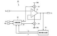
- FIG. 2 is a diagram showing a first output circuit included in the data line drive circuit shown in FIG. 1;
- FIG. 6 is a diagram showing a second output circuit included in the data line drive circuit shown in FIG. 1.
- FIG. 1 It is a figure which shows the change of the output signal of the data line drive circuit in the liquid crystal display device shown in FIG. It is a figure which shows the method of providing an output circuit in the data line drive circuit of the liquid crystal display device which concerns on 2nd Embodiment. It is a block diagram which shows the structure of the conventional liquid crystal display device. It is a figure which shows the change of the output signal of the data line drive circuit in the conventional liquid crystal display device.
- FIG. 1 is a block diagram showing the configuration of the liquid crystal display device according to the first embodiment.
- the liquid crystal display device 10 shown in FIG. 1 includes a liquid crystal panel 11, a display control circuit 12, two scanning line driving circuits 13a and 13b, and four data line driving circuits 14a to 14d.
- the scanning line driving circuits 13a and 13b and the data line driving circuits 14a to 14d are respectively incorporated in an IC chip.
- the horizontal direction of the drawing is referred to as the row direction
- the vertical direction of the drawing is referred to as the column direction.
- a display area 15 is set in the liquid crystal panel 11.
- a plurality of scan lines, a plurality of data lines, and a plurality of pixel circuits are formed in the display area 15.
- the scanning line Gi, the data line Sj, and the pixel circuit Pij are described in FIG.
- the plurality of scan lines extend in the row direction and are arranged parallel to one another.
- the plurality of data lines extend in the column direction and are arranged parallel to one another so as to be orthogonal to the scan lines.
- the plurality of pixel circuits are two-dimensionally arranged corresponding to the intersections of the scanning lines and the data lines.
- the pixel circuit Pij includes a thin film transistor (hereinafter referred to as a TFT) 16 and a liquid crystal capacitor 17.
- the gate terminal of the TFT 16 is connected to the scanning line Gi.
- One conduction terminal (terminal on the left side in FIG. 1) of the TFT 16 is connected to the data line Sj.
- the other conduction terminal of the TFT 16 is connected to one electrode (upper electrode in FIG. 1) of the liquid crystal capacitor 17.
- the common electrode Vcom is applied to the other electrode of the liquid crystal capacitor 17.
- the pixel circuit Pij may include an auxiliary capacitance in parallel with the liquid crystal capacitance 17.
- the display control circuit 12 is provided outside the liquid crystal panel 11.
- the display control circuit 12 outputs the timing signal TS1 to the scanning line drive circuits 13a and 13b based on the video signal VS1 supplied from the host device (not shown), and the data control circuit 14a to 14d.
- the timing signal TS2 and the video signal VS2 are output.
- the scanning line drive circuits 13 a and 13 b are disposed on the liquid crystal panel 11 at the periphery of the display area 15.
- the scanning line drive circuits 13 a and 13 b are arranged along the right side of the display area 15.
- the scanning line drive circuits 13a and 13b drive the scanning lines based on the timing signal TS1. More specifically, the scanning line driving circuits 13a and 13b select one scanning line from the plurality of scanning lines based on the timing signal TS1, and the voltage at which the TFT 16 turns on the selected scanning line (high level voltage Apply).
- the display area 15 is divided into an upper half and a lower half.
- the scanning line driving circuit 13 a drives scanning lines disposed in the upper half of the display area 15, and the scanning line driving circuit 13 b drives scanning lines disposed in the lower half of the display area 15.
- the data line drive circuits 14 a to 14 d are arranged on the liquid crystal panel 11 at the periphery of the display area 15. In FIG. 1, the data line drive circuits 14 a to 14 d are arranged along the lower side of the display area 15. The data line drive circuits 14a to 14d drive the data lines based on the timing signal TS2 and the video signal VS2. More specifically, the data line drive circuits 14a to 14d apply a plurality of voltages corresponding to the video signal VS2 to the plurality of data lines based on the timing signal TS2.
- the display area 15 is divided into four parts in the horizontal direction corresponding to the data line drive circuits 14a to 14d. Data line drive circuits 14a-14d respectively drive corresponding data lines (data lines arranged in corresponding portions of display area 15).
- Data line drive circuits 14a-14d have a plurality of output circuits corresponding to corresponding data lines. More specifically, data line drive circuits 14a-14d each have one of a first output circuit and a second output circuit corresponding to each corresponding data line. For example, when the data line drive circuit 14a drives 1440 data lines, the data line drive circuit 14a has 1440 in total of the first output circuit and the second output circuit.
- FIG. 2 is a circuit diagram of the first output circuit.
- a first output circuit 20 corresponding to the data line Sj is shown in FIG.
- the first output circuit 20 includes a differential amplifier 21, a control circuit 22, bias current sources 23 and 24, and a slope detection circuit 25.
- An analog voltage Va based on the video signal VS2 is supplied to the non-inversion input terminal of the differential amplifier 21.
- the inverting input terminal of the differential amplifier 21 is connected to the output terminal of the differential amplifier 21.
- the output terminal of the differential amplifier 21 is connected to the data line Sj.
- the control circuit 22 outputs two bias current control signals C1 and C2 based on the output level signal LV, the polarity signal POL and the output signal of the inclination detection circuit 25.
- the bias current source 23 is provided between the power supply line supplying the high level power supply voltage VDD and the positive side power supply terminal of the differential amplifier 21.
- the bias current source 23 controls the amount of positive bias current supplied to the differential amplifier 21 based on the bias current control signal C1.
- the bias current source 24 is provided between the power supply line for supplying the low level power supply voltage VSS and the negative side power supply terminal of the differential amplifier 21.
- the bias current source 24 controls the amount of negative bias current supplied to the differential amplifier 21 based on the bias current control signal C2.
- the input terminal of the inclination detection circuit 25 is connected to the output terminal of the differential amplifier 21 and the data line Sj.
- the inclination detection circuit 25 detects the inclination when the output signal of the data line drive circuit 14 rises and the inclination when the output signal of the data line drive circuit 14 falls (hereinafter referred to as the inclination when rising the former, The latter is called the falling slope).
- the inclination detection circuit 25 outputs an inclination detection signal Tr indicating the inclination at the rising edge and an inclination detection signal Tf indicating the inclination at the falling edge.
- the inclination detection signals Tr and Tf are used when the control circuit 22 obtains the bias current control signals C1 and C2.
- FIG. 3 is a circuit diagram of a second output circuit.
- a second output circuit 30 corresponding to the data line Sk is shown in FIG.
- the second output circuit 30 is obtained by removing the inclination detection circuit 25 from the first output circuit 20.
- the control circuit 22 of the second output circuit 30 is supplied with the inclination detection signals Tr and Tf output from the inclination detection circuit 25 included in the first output circuit 20 corresponding to the other data line.
- the inclination detection circuit 25 detects the inclination of the output signal of the data line drive circuit 14 (the signal on the data line).
- the control circuit 22 and the bias current sources 23 and 24 function as a slope control circuit that controls the slope of the output signal of the data line drive circuit 14 based on the slope detected by the slope detection circuit 25.
- the slope control circuit controls the bias current supplied to the differential amplifier 21 based on the slope detected by the slope detection circuit 25.
- a second output circuit 30 having a slope control circuit for controlling the slope of the output signal of the data line drive circuit 14.
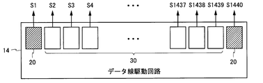
- FIG. 4 to 6 are diagrams showing an example of a method of providing an output circuit in the data line drive circuit 14.
- the data line driving circuit 14 drives 1440 data lines S1 to S1440.
- the data line drive circuit 14 is provided with the first output circuit 20 corresponding to the data lines at both ends of the corresponding data lines, and the second output circuit corresponding to the remaining data lines.
- An output circuit 30 is provided. Specifically, two first output circuits 20 are provided corresponding to data lines S1 and S1440, and a total of 1438 second output circuits 30 are provided corresponding to data lines S2 to S1439. .
- the control circuit 22 of the second output circuit 30 receives the inclination detection signals Tr and Tf output from the first output circuit 20 corresponding to the data line S1, and the first output circuit 20 corresponding to the data line S1440.
- One or both of the inclination detection signals Tr and Tf output from the circuit are supplied.
- the former may be supplied to the second output circuit 30 corresponding to the data lines S2 to S720, and the latter may be supplied to the second output circuit 30 corresponding to the data lines S721 to S1439.
- both may be supplied to the second output circuit 30 corresponding to the data lines S2 to S1439.
- data line drive circuit 14 is provided with first output circuit 20 corresponding to the data line at both ends and the center among corresponding data lines, and corresponding to the remaining data lines.
- a second output circuit 30 is provided. Specifically, three first output circuits 20 are provided corresponding to data lines S1 and S1440 at both ends and data line S721 at the center, and all of them are provided corresponding to data lines S2 to S720 and S722 to S1439. , And 1437 second output circuits 30 are provided.
- the control circuit 22 of the second output circuit 30 corresponding to the data lines S2 to S720 the inclination detection signals Tr and Tf output from the first output circuit 20 corresponding to the data line S1 and the data line S721. And one or both of the inclination detection signals Tr and Tf output from the first output circuit 20 corresponding to.
- the control circuit 22 of the second output circuit 30 corresponding to the data lines S722 to S1439 corresponds to the inclination detection signals Tr and Tf output from the first output circuit 20 corresponding to the data line S721 and the data line S1440.
- One or both of the inclination detection signals Tr and Tf output from the first output circuit 20 are supplied.
- the data line drive circuit 14 is provided with the first output circuit 20 corresponding to the odd-numbered data line among the corresponding data lines, and corresponding to the even-numbered data line.
- a second output circuit 30 is provided. Specifically, a total of 720 first output circuits 20 are provided corresponding to data lines S1, S3,..., S1439, and a total of 720 corresponding to data lines S2, S4,.
- a second output circuit 30 is provided.
- the control circuit 22 of the second output circuit 30 corresponding to the even-numbered data line receives the inclination detection signals Tr, Tf, and Tf output from the first output circuit 20 corresponding to the immediately preceding data line.
- One or both of the inclination detection signals Tr and Tf output from the first output circuit 20 corresponding to the next data line are supplied.
- the first output circuit 20 is provided corresponding to the even-numbered data line among the corresponding data lines
- the second output circuit 30 is provided corresponding to the odd-numbered data line. It is also good.
- control circuit 22 included in the second output circuit 30 controls the bias current control signal based on the output level signal LV, the polarity signal POL, and the supplied inclination detection signals Tr and Tr. Output C1 and C2.
- the inclination detection circuit 25 detects the inclination at the time of rising and the inclination at the time of falling for the output signal of the data line driving circuit 14.
- the control circuit 22 included in the first and second output circuits 20 and 30 determines the amount of positive bias current output from the bias current source 23 and the bias current source 24 based on the slope detected by the slope detection circuit 25. Control the amount of negative bias current output.
- the positive bias current increases, the rising slope of the output signal of the data line driving circuit 14 becomes larger (sudden).
- the positive bias current decreases, the rising slope of the output signal of the data line driving circuit 14 decreases (becomes gradual).
- the negative bias current increases, the absolute value of the falling slope of the output signal of the data line driving circuit 14 becomes larger (steep).
- the negative bias current decreases, the absolute value of the falling slope of the output signal of the data line driving circuit 14 decreases (becomes gradual).
- target values of the rising inclination and the falling inclination of the output signal of the data line driving circuit 14 are predetermined, and the amount of positive bias current and the negative bias are determined based on the inclination detected by the inclination detection circuit 25.
- the amount of current it is possible to bring the inclination at the rise and the inclination at the fall of the output signal of the data line drive circuit 14 closer to their respective target values. Therefore, it is possible to equalize the changing speed and the reaching level of the output signal among the data line driving circuits 14a to 14d, and to prevent the occurrence of the block-like luminance unevenness on the display screen. In addition, these effects can be achieved without adding a new wiring to the liquid crystal panel 11.
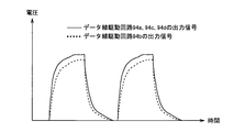
- FIG. 7 is a diagram showing changes in the output signal of the data line drive circuit in the liquid crystal display device 10.
- the output signal of the data line drive circuit 94b changes more slowly than the output signals of the data line drive circuits 94a, 94c and 94d (see FIG. 10).
- the output signal of the data line drive circuit 14b (broken line) is obtained by bringing the inclination at the rise and fall inclination of the output signal of the data line drive circuit 14 closer to their respective target values. Changes at substantially the same speed as the output signals (solid lines) of the data line drive circuits 14a, 14c, and 14d.
- the former reaches almost the same level as the latter. Therefore, without adding a new wiring to the liquid crystal panel 11, the change speed and reaching level of the output signal are made equal among the data line drive circuits 14a to 14d, and the occurrence of block-like luminance unevenness on the display screen is prevented. can do.
- the detection and adjustment of the inclination are performed, for example, in an inspection process before shipment of the liquid crystal display device 10.
- a test pattern is used which changes the output signal of the data line drive circuit between a relatively low level and a relatively high level.
- the test pattern preferably changes the output signal of the data line drive circuit between the lowest level and the highest level.
- a test pattern may be used in which a black image and a white image are alternately displayed for each frame.
- line inversion driving or dot inversion driving a test pattern may be used to display an image including black lines and white lines alternately.
- the inclination detection circuit 25 detects the inclination at the rising and the inclination at the falling when the test pattern is displayed on the screen, and detects the inclination detection signals Tr and Tf. Output The control circuit 22 internally holds the output inclination detection signals Tr and Tf. When the liquid crystal display device 10 is shipped and actually used, the control circuit 22 outputs the bias current control signals C1 and C2 based on the output level signal LV, the polarity signal POL and the tilt detection signals Tr and Tf held. Do. Thereby, based on the inclination detected in the inspection process of the liquid crystal display device 10, it is possible to prevent block-like luminance unevenness from occurring in the display screen when the liquid crystal display device 10 is used.
- the tilt detection and adjustment may be performed after shipment of the liquid crystal display device 10.
- the liquid crystal display device 10 may enter a test mode when the power is turned on, and may perform tilt detection and adjustment in the test mode.
- the liquid crystal display device 10 may enter a test mode in accordance with an instruction from the user, and may perform inclination detection and adjustment in the test mode.
- the first output circuit 20 is provided in the data line drive circuit 14, and the inclination of the output signal of the data line drive circuit 14 is detected.
- the changing speed and the reaching level of the output signal of the data line driving circuit 14 are equalized, and high quality display can be realized without providing new wiring in the display panel. It can be carried out.
- the second output circuit 30 in the data line drive circuit 14 the above-described effect can be achieved without significantly increasing the number of circuits.
- the increase amount of the circuit can be reduced.
- the liquid crystal display device according to the second embodiment has the same configuration as the liquid crystal display device according to the first embodiment (see FIG. 1). Hereinafter, differences from the first embodiment will be described.
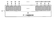
- FIG. 8 is a view showing a method of providing an output circuit in the data line drive circuit 14 of the liquid crystal display device according to the present embodiment.
- the data line driving circuit 14 drives 1440 data lines S1 to S1440.
- the first output circuit 20 is provided corresponding to all of the corresponding data lines. Specifically, a total of 1440 first output circuits 20 are provided corresponding to data lines S1 to S1440.
- the same effect as the liquid crystal display device 10 according to the first embodiment can be obtained.
- high quality display can be performed. For example, if the resistance of one data line is higher than the resistance of another data line, the data line drive circuit 14 drives the output signal of the data line with a higher driving power than the output signal of the other data line. Just do it.
- a liquid crystal display device provided with only one data line drive circuit 14 may be configured.
- the same effect as the liquid crystal display device according to the second embodiment can also be achieved by the liquid crystal display device according to the modification.
- the liquid crystal display device has been described above as an example of the display device, a display device other than the liquid crystal display device may be configured in the same manner.
- SYMBOLS 10 Liquid crystal display device 11 ... Liquid crystal panel 12 ... Display control circuit 13 ... Scanning line drive circuit 14 ... Data line drive circuit 15 ... Display area 16 ... TFT DESCRIPTION OF SYMBOLS 17 ... Liquid crystal capacity 20 ... 1st output circuit 21 ... Differential amplifier 22 ... Control circuit 23, 24 ... Bias current source 25 ... Inclination detection circuit 30 ... 2nd output circuit
Landscapes
- Physics & Mathematics (AREA)
- Engineering & Computer Science (AREA)
- General Physics & Mathematics (AREA)
- Chemical & Material Sciences (AREA)
- Crystallography & Structural Chemistry (AREA)
- Computer Hardware Design (AREA)
- Theoretical Computer Science (AREA)
- Nonlinear Science (AREA)
- Mathematical Physics (AREA)
- Optics & Photonics (AREA)
- Control Of Indicators Other Than Cathode Ray Tubes (AREA)
- Liquid Crystal Display Device Control (AREA)
Abstract
表示装置のデータ線駆動回路にデータ線の一部または全部に対応して、出力信号の傾きを検出する傾き検出回路と、傾き検出回路で検出された傾きに基づき出力信号の傾きを制御する傾き制御回路とを有する第1出力回路を設ける。残余のデータ線に対応して、第1出力回路に含まれる傾き検出回路で検出された傾きに基づき出力信号の傾きを制御する傾き制御回路を有する第2出力回路を設ける。これにより、データ線駆動回路の出力信号の変化速度と到達レベルを揃え、表示パネルに新たな配線を設けることなく高品位の表示を行う。
Description
本発明は、表示装置、および、表示装置のデータ線駆動回路に関する。
液晶表示装置は、薄型、軽量、低消費電力の表示装置として広く利用されている。液晶表示装置の液晶パネルには、複数の走査線、複数のデータ線、および、複数の画素回路が形成される。また、液晶表示装置には、走査線を駆動する走査線駆動回路と、データ線を駆動するデータ線駆動回路とが設けられる。データ線はソース線、データ線駆動回路はソースドライバとも呼ばれる。
データ線の本数が多い液晶表示装置には、データ線を駆動するために、データ線駆動回路を内蔵した複数のICチップが設けられる。例えば、図9に示す液晶表示装置には、ICチップに内蔵された4個のデータ線駆動回路94a~94dが設けられている。液晶パネル91の表示領域95は、4個の部分に分割される。データ線駆動回路94a~94dは、それぞれ、表示領域95の対応する部分に配置されたデータ線を駆動する。
図9に示す液晶表示装置では、データ線駆動回路94a~94dの間で、ICチップ内の配線の抵抗がばらついたり、液晶パネル91上の配線の抵抗がばらついたりする。このため、あるデータ線駆動回路によって駆動されるデータ線の電圧と、他のデータ線駆動回路によって駆動されるデータ線の電圧との間に差が生じる。
図10は、図9に示す液晶表示装置におけるデータ線駆動回路の出力信号の変化を示す図である。この例では、データ線駆動回路94bの出力信号(破線)は、データ線駆動回路94a、94c、94dの出力信号(実線)よりも緩慢に変化する。このため、前者は後者よりも低いレベルにしか到達しない。この結果、図9に示すように、表示画面内にICチップに対応したブロック状の輝度むらが発生する。ブロック状の輝度むらは、白画像や黒画像を表示するときには認識されにくいが、中間調画像(例えば、グレー画像)を表示するときには認識されやすい。
特許文献1には、ソース配線の負荷がばらつく場合でも良好な表示を行うために、液晶パネルのアレイ基板(画素回路などが形成される基板)にソース配線に接続されたフィードバック配線を設け、フィードバック配線の測定結果に基づき、ソースドライバICに含まれる複数の出力バッファの中の1つを選択する液晶表示装置が記載されている。
しかしながら、特許文献1に記載された液晶表示装置では、液晶パネルのアレイ基板にフィードバック配線を新たに設ける必要がある。
それ故に、表示パネルに新たな配線を設けることなく高品位の表示を行う表示装置を提供することが課題として挙げられる。
上記の課題は、例えば、複数の走査線と、複数のデータ線と、複数の画素回路とを含む表示パネルと、走査線を駆動する走査線駆動回路と、データ線を駆動するデータ線駆動回路とを備え、データ線駆動回路は、データ線に対応して複数の出力回路を含み、出力回路の中に、出力信号の傾きを検出する傾き検出回路と、傾き検出回路で検出された傾きに基づき出力信号の傾きを制御する傾き制御回路とを有する第1出力回路が含まれている表示装置によって解決することができる。上記の課題は、上記の表示装置に含まれるデータ線駆動回路によっても解決することができる。
上記の表示装置またはデータ線駆動回路によれば、データ線駆動回路の出力信号の傾きを検出し、検出した傾きに基づきデータ線駆動回路の出力信号の傾きを制御することにより、データ線駆動回路の出力信号(データ線上の信号)の変化速度と到達レベルを揃え、表示パネルに新たな配線を設けることなく高品位の表示を行うことができる。
(第1の実施形態)
図1は、第1の実施形態に係る液晶表示装置の構成を示すブロック図である。図1に示す液晶表示装置10は、液晶パネル11、表示制御回路12、2個の走査線駆動回路13a、13b、および、4個のデータ線駆動回路14a~14dを備えている。走査線駆動回路13a、13bとデータ線駆動回路14a~14dは、それぞれ、ICチップに内蔵されている。以下、図面の水平方向を行方向、図面の垂直方向を列方向という。
図1は、第1の実施形態に係る液晶表示装置の構成を示すブロック図である。図1に示す液晶表示装置10は、液晶パネル11、表示制御回路12、2個の走査線駆動回路13a、13b、および、4個のデータ線駆動回路14a~14dを備えている。走査線駆動回路13a、13bとデータ線駆動回路14a~14dは、それぞれ、ICチップに内蔵されている。以下、図面の水平方向を行方向、図面の垂直方向を列方向という。
液晶パネル11には、表示領域15が設定される。表示領域15の内部には、複数の走査線、複数のデータ線、および、複数の画素回路が形成される。図1には、このうち走査線Gi、データ線Sj、および、画素回路Pijが記載されている。複数の走査線は、行方向に延伸し、互いに平行に配置される。複数のデータ線は、列方向に延伸し、走査線と直交するように互いに平行に配置される。複数の画素回路は、走査線とデータ線の交点に対応して2次元状に配置される。
画素回路Pijは、薄膜トランジスタ(Thin Film Transistor:以下、TFTという)16と液晶容量17を含んでいる。TFT16のゲート端子は、走査線Giに接続される。TFT16の一方の導通端子(図1では左側の端子)は、データ線Sjに接続される。TFT16の他方の導通端子は、液晶容量17の一方の電極(図1では上側の電極)に接続される。液晶容量17の他方の電極には、共通電極Vcomが印加される。なお、画素回路Pijは、液晶容量17と並列に補助容量を含んでいてもよい。
表示制御回路12は、液晶パネル11の外部に設けられる。表示制御回路12は、ホスト装置(図示せず)から供給された映像信号VS1に基づき、走査線駆動回路13a、13bに対してタイミング信号TS1を出力し、データ線駆動回路14a~14dに対してタイミング信号TS2と映像信号VS2を出力する。
走査線駆動回路13a、13bは、液晶パネル11上で表示領域15の周辺部に配置される。図1では、走査線駆動回路13a、13bは、表示領域15の右辺に沿って並べて配置されている。走査線駆動回路13a、13bは、タイミング信号TS1に基づき走査線を駆動する。より詳細には、走査線駆動回路13a、13bは、タイミング信号TS1に基づき、複数の走査線の中から1本の走査線を選択し、選択した走査線にTFT16がオンする電圧(ハイレベル電圧)を印加する。表示領域15は、上半分と下半分に分割される。走査線駆動回路13aは表示領域15の上半分に配置された走査線を駆動し、走査線駆動回路13bは表示領域15の下半分に配置された走査線を駆動する。
データ線駆動回路14a~14dは、液晶パネル11上で表示領域15の周辺部に配置される。図1では、データ線駆動回路14a~14dは、表示領域15の下辺に沿って並べて配置されている。データ線駆動回路14a~14dは、タイミング信号TS2と映像信号VS2に基づきデータ線を駆動する。より詳細には、データ線駆動回路14a~14dは、タイミング信号TS2に基づき、映像信号VS2に応じた複数の電圧を複数のデータ線に印加する。表示領域15は、データ線駆動回路14a~14dに対応して、水平方向に4個の部分に分割される。データ線駆動回路14a~14dは、それぞれ、対応するデータ線(表示領域15の対応する部分に配置されたデータ線)を駆動する。
データ線駆動回路14a~14dは、対応するデータ線に対応して複数の出力回路を有する。より詳細には、データ線駆動回路14a~14dは、対応するデータ線のそれぞれに対応して、第1出力回路および第2出力回路のいずれか一方を有する。例えば、データ線駆動回路14aが1440本のデータ線を駆動する場合、データ線駆動回路14aは第1出力回路と第2出力回路を合わせて1440個有する。
図2は、第1出力回路の回路図である。図2には、データ線Sjに対応した第1出力回路20が記載されている。第1出力回路20は、差動増幅器21、制御回路22、バイアス電流源23、24、および、傾き検出回路25を含んでいる。差動増幅器21の非反転入力端子には、映像信号VS2に基づくアナログ電圧Vaが供給される。差動増幅器21の反転入力端子は、差動増幅器21の出力端子に接続される。差動増幅器21の出力端子は、データ線Sjに接続される。
制御回路22は、出力レベル信号LVと極性信号POLと傾き検出回路25の出力信号とに基づき、2個のバイアス電流制御信号C1、C2を出力する。バイアス電流源23は、ハイレベル電源電圧VDDを供給する電源配線と差動増幅器21の正側電源端子との間に設けられる。バイアス電流源23は、バイアス電流制御信号C1に基づき、差動増幅器21に供給される正バイアス電流の量を制御する。バイアス電流源24は、ローレベル電源電圧VSSを供給する電源配線と差動増幅器21の負側電源端子との間に設けられる。バイアス電流源24は、バイアス電流制御信号C2に基づき、差動増幅器21に供給される負バイアス電流の量を制御する。
傾き検出回路25の入力端子は、差動増幅器21の出力端子とデータ線Sjに接続される。傾き検出回路25は、データ線駆動回路14の出力信号が上昇するときの傾きと、データ線駆動回路14の出力信号が降下するときの傾きとを検出する(以下、前者を立ち上がり時の傾き、後者を立ち下がり時の傾きという)。傾き検出回路25は、立ち上がり時の傾きを示す傾き検出信号Trと、立ち下がり時の傾きを示す傾き検出信号Tfとを出力する。傾き検出信号Tr、Tfは、制御回路22においてバイアス電流制御信号C1、C2を求めるときに使用される。
図3は、第2出力回路の回路図である。図3には、データ線Skに対応した第2出力回路30が記載されている。第2出力回路30は、第1出力回路20から傾き検出回路25を削除したものである。第2出力回路30の制御回路22には、他のデータ線に対応した第1出力回路20に含まれる傾き検出回路25から出力された傾き検出信号Tr、Tfが供給される。
第1および第2出力回路20、30において、傾き検出回路25はデータ線駆動回路14の出力信号(データ線上の信号)の傾きを検出する。制御回路22とバイアス電流源23、24は、傾き検出回路25で検出された傾きに基づきデータ線駆動回路14の出力信号の傾きを制御する傾き制御回路として機能する。傾き制御回路は、傾き検出回路25で検出された傾きに基づき、差動増幅器21に供給されるバイアス電流を制御する。データ線駆動回路14に設けられる出力回路の中には、傾き検出回路25と傾き制御回路とを有する第1出力回路20と、第1出力回路20に含まれる傾き検出回路25で検出された傾きに基づき、データ線駆動回路14の出力信号の傾きを制御する傾き制御回路を有する第2出力回路30とが含まれる。
図4~図6は、データ線駆動回路14に出力回路を設ける方法の例を示す図である。ここでは、データ線駆動回路14は、1440本のデータ線S1~S1440を駆動するものとする。第1例(図4)では、データ線駆動回路14には、対応するデータ線のうち両端のデータ線に対応して第1出力回路20が設けられ、残余のデータ線に対応して第2出力回路30が設けられる。具体的には、データ線S1、S1440に対応して合わせて2個の第1出力回路20が設けられ、データ線S2~S1439に対応して全部で1438個の第2出力回路30が設けられる。
この場合、第2出力回路30の制御回路22には、データ線S1に対応した第1出力回路20から出力された傾き検出信号Tr、Tf、および、データ線S1440に対応した第1出力回路20から出力された傾き検出信号Tr、Tfのいずれか一方、または、両方が供給される。例えば、データ線S2~S720に対応した第2出力回路30には前者を供給し、データ線S721~S1439に対応した第2出力回路30には後者を供給してもよい。あるいは、データ線S2~S1439に対応した第2出力回路30に両者を供給してもよい。
第2例(図5)では、データ線駆動回路14には、対応するデータ線のうち両端と中央のデータ線に対応して第1出力回路20が設けられ、残余のデータ線に対応して第2出力回路30が設けられる。具体的には、両端のデータ線S1、S1440と中央のデータ線S721に対応して合わせて3個の第1出力回路20が設けられ、データ線S2~S720、S722~S1439に対応して全部で1437個の第2出力回路30が設けられる。
この場合、データ線S2~S720に対応した第2出力回路30の制御回路22には、データ線S1に対応した第1出力回路20から出力された傾き検出信号Tr、Tf、および、データ線S721に対応した第1出力回路20から出力された傾き検出信号Tr、Tfのいずれか一方、または、両方が供給される。データ線S722~S1439に対応した第2出力回路30の制御回路22には、データ線S721に対応した第1出力回路20から出力された傾き検出信号Tr、Tf、および、データ線S1440に対応した第1出力回路20から出力された傾き検出信号Tr、Tfのいずれか一方、または、両方が供給される。
第3例(図6)では、データ線駆動回路14には、対応するデータ線のうち奇数番目のデータ線に対応して第1出力回路20が設けられ、偶数番目のデータ線に対応して第2出力回路30が設けられる。具体的には、データ線S1、S3、…、S1439に対応して全部で720個の第1出力回路20が設けられ、データ線S2、S4、…、S1440に対応して全部で720個の第2出力回路30が設けられる。
この場合、偶数番目のデータ線に対応した第2出力回路30の制御回路22には、1つ前のデータ線に対応した第1出力回路20から出力された傾き検出信号Tr、Tf、および、1つ後のデータ線に対応した第1出力回路20から出力された傾き検出信号Tr、Tfのいずれか一方、または、両方が供給される。なお、データ線駆動回路14には、対応するデータ線のうち偶数番目のデータ線に対応して第1出力回路20を設け、奇数番目のデータ線に対応して第2出力回路30を設けてもよい。
第1~第3例のいずれにおいても、第2出力回路30に含まれる制御回路22は、出力レベル信号LVと極性信号POLと供給された傾き検出信号Tr、Trとに基づき、バイアス電流制御信号C1、C2を出力する。
傾き検出回路25は、データ線駆動回路14の出力信号について立ち上がり時の傾きと立ち下がり時の傾きとを検出する。第1および第2出力回路20、30に含まれる制御回路22は、傾き検出回路25で検出された傾きに基づき、バイアス電流源23から出力される正バイアス電流の量と、バイアス電流源24から出力される負バイアス電流の量とを制御する。正バイアス電流が増加すると、データ線駆動回路14の出力信号の立ち上がり時の傾きは大きくなる(急になる)。正バイアス電流が減少すると、データ線駆動回路14の出力信号の立ち上がり時の傾きは小さくなる(緩やかになる)。負バイアス電流が増加すると、データ線駆動回路14の出力信号の立ち下がり時の傾きの絶対値は大きくなる(急になる)。負バイアス電流が減少すると、データ線駆動回路14の出力信号の立ち下がり時の傾きの絶対値は小さくなる(緩やかになる)。
そこで、データ線駆動回路14の出力信号の立ち上がり時の傾きと立ち下がり時の傾きの目標値を予め定めておき、傾き検出回路25で検出された傾きに基づき、正バイアス電流の量と負バイアス電流の量を制御することにより、データ線駆動回路14の出力信号の立ち上がり時の傾きと立ち下がり時の傾きをそれぞれの目標値に近づけることができる。したがって、データ線駆動回路14a~14dの間で出力信号の変化速度と到達レベルを揃え、表示画面にブロック状の輝度むらが発生することを防止することができる。また、液晶パネル11に新たな配線を追加することなく、これらの効果を奏することができる。
図7は、液晶表示装置10におけるデータ線駆動回路の出力信号の変化を示す図である。上述したように、従来の液晶表示装置では、データ線駆動回路94bの出力信号は、データ線駆動回路94a、94c、94dの出力信号よりも緩慢に変化する(図10を参照)。これに対して液晶表示装置10では、データ線駆動回路14の出力信号の立ち上がり時の傾きと立ち下がり時の傾きをそれぞれの目標値に近づけることにより、データ線駆動回路14bの出力信号(破線)は、データ線駆動回路14a、14c、14dの出力信号(実線)とほぼ同じ速度で変化する。したがって、前者は後者とほぼ同じにレベルに到達する。よって、液晶パネル11に新たな配線を追加することなく、データ線駆動回路14a~14dの間で出力信号の変化速度と到達レベルを揃え、表示画面にブロック状の輝度むらが発生することを防止することができる。
傾きの検出と調整は、例えば、液晶表示装置10の出荷前の検査工程で行われる。傾きを検出するときには、データ線駆動回路の出力信号を相対的に低いレベルと相対的に高いレベルとの間で変化させるテストパターンが使用される。テストパターンは、データ線駆動回路の出力信号を最低レベルと最高レベルとの間で変化させることが好ましい。液晶表示装置がフレーム反転駆動を行う場合には、黒画像と白画像をフレームごとに交互に表示させるテストパターンを用いればよい。液晶表示装置がライン反転駆動またはドット反転駆動を行う場合には、黒ラインと白ラインを交互に含む画像を表示させるテストパターンを用いればよい。
液晶表示装置10の検査工程において、傾き検出回路25は、上記のテストパターンが画面に表示されているときに、立ち上がり時の傾きと立ち下がり時の傾きとを検出し、傾き検出信号Tr、Tfを出力する。制御回路22は、出力された傾き検出信号Tr、Tfを内部に保持する。液晶表示装置10が出荷され、実際に使用されるときには、制御回路22は、出力レベル信号LVと極性信号POLと保持した傾き検出信号Tr、Tfとに基づき、バイアス電流制御信号C1、C2を出力する。これにより、液晶表示装置10の検査工程で検出した傾きに基づき、液晶表示装置10の使用時に表示画面内にブロック状の輝度むらが発生することを防止することができる。
なお、傾きの検出と調整を液晶表示装置10の出荷後に行ってもよい。例えば、液晶表示装置10は、電源投入時にテストモードに入り、テストモードにおいて傾きの検出と調整を行ってもよい。また、液晶表示装置10は、利用者からの指示に従いテストモードに入り、テストモードにおいて傾きの検出と調整を行ってもよい。
本実施形態に係る液晶表示装置10によれば、データ線駆動回路14に第1出力回路20を設け、データ線駆動回路14の出力信号の傾きを検出し、検出した傾きに基づきデータ線駆動回路14の出力信号の傾きを制御することにより、データ線駆動回路14の出力信号(データ線上の信号)の変化速度と到達レベルを揃え、表示パネルに新たな配線を設けることなく高品位の表示を行うことができる。また、データ線駆動回路14に第2出力回路30を設けることにより、回路を大幅に増加させることなく上記の効果を奏することができる。特に、第1および第2例のようにデータ線駆動回路14に出力回路を設けることにより、回路の増加量を小さくすることができる。
(第2の実施形態)
第2の実施形態に係る液晶表示装置は、第1の実施形態に係る液晶表示装置と同じ構成を有する(図1を参照)。以下、第1の実施形態との相違点を説明する。
第2の実施形態に係る液晶表示装置は、第1の実施形態に係る液晶表示装置と同じ構成を有する(図1を参照)。以下、第1の実施形態との相違点を説明する。
図8は、本実施形態に係る液晶表示装置のデータ線駆動回路14に出力回路を設ける方法を示す図である。ここでは、データ線駆動回路14は、1440本のデータ線S1~S1440を駆動するものとする。本実施形態に係るデータ線駆動回路14には、対応するデータ線のすべてに対応して第1出力回路20が設けられる。具体的には、データ線S1~S1440に対応して全部で1440個の第1出力回路20が設けられる。
本実施形態に係る液晶表示装置によれば、第1の実施形態に係る液晶表示装置10と同じ効果を奏することができる。また、データ線の特性にばらつきがある場合でも、高品位の表示を行うことができる。例えば、あるデータ線の抵抗が他のデータ線の抵抗と比べて高い場合には、データ線駆動回路14は当該データ線の出力信号を他のデータ線の出力信号よりも高い駆動能力で駆動すればよい。
なお、第2の実施形態の変形例として、データ線駆動回路14を1個だけ備えた液晶表示装置を構成してもよい。変形例に係る液晶表示装置によっても、第2の実施形態に係る液晶表示装置と同じ効果を奏することができる。また、ここまで表示装置の例として液晶表示装置について説明してきたが、同様の方法で液晶表示装置以外の表示装置を構成してもよい。
本願は、2017年6月21日に出願された「表示装置およびデータ線駆動回路」という名称の日本国特願2017-121041号に基づく優先権を主張する出願であり、この出願の内容は引用することによって本願の中に含まれる。
10…液晶表示装置
11…液晶パネル
12…表示制御回路
13…走査線駆動回路
14…データ線駆動回路
15…表示領域
16…TFT
17…液晶容量
20…第1出力回路
21…差動増幅器
22…制御回路
23、24…バイアス電流源
25…傾き検出回路
30…第2出力回路
11…液晶パネル
12…表示制御回路
13…走査線駆動回路
14…データ線駆動回路
15…表示領域
16…TFT
17…液晶容量
20…第1出力回路
21…差動増幅器
22…制御回路
23、24…バイアス電流源
25…傾き検出回路
30…第2出力回路
Claims (12)
- 複数の走査線と、複数のデータ線と、複数の画素回路とを含む表示パネルと、
前記走査線を駆動する走査線駆動回路と、
前記データ線を駆動するデータ線駆動回路とを備え、
前記データ線駆動回路は、前記データ線に対応して複数の出力回路を含み、
前記出力回路の中に、出力信号の傾きを検出する傾き検出回路と、前記傾き検出回路で検出された傾きに基づき前記出力信号の傾きを制御する傾き制御回路とを有する第1出力回路が含まれていることを特徴とする、表示装置。 - 前記出力回路の中に、前記第1出力回路に含まれる傾き検出回路で検出された傾きに基づき出力信号の傾きを制御する傾き制御回路を有する第2出力回路が含まれていることを特徴とする、請求項1に記載の表示装置。
- 前記データ線のうち対応するデータ線を駆動する複数のデータ線駆動回路を備えることを特徴とする、請求項2に記載の表示装置。
- 各前記データ線駆動回路は、前記対応するデータ線のうち両端のデータ線に対応して前記第1出力回路を含み、残余のデータ線に対応して前記第2出力回路を含むことを特徴とする、請求項3に記載の表示装置。
- 各前記データ線駆動回路は、前記対応するデータ線のうち両端と中央のデータ線に対応して前記第1出力回路を含み、残余のデータ線に対応して前記第2出力回路を含むことを特徴とする、請求項3に記載の表示装置。
- 各前記データ線駆動回路は、前記対応するデータ線のうち奇数番目および偶数番目のいずれか一方のデータ線に対応して前記第1出力回路を含み、残余のデータ線に対応して前記第2出力回路を含むことを特徴とする、請求項3に記載の表示装置。
- 前記データ線のうち対応するデータ線を駆動する複数のデータ線駆動回路を備え、
各前記データ線駆動回路は、前記対応するデータ線のすべてに対応して前記第1出力回路を含むことを特徴とする、請求項1に記載の表示装置。 - 前記データ線駆動回路は、前記データ線のすべてに対応して前記第1出力回路を含むことを特徴とする、請求項1に記載の表示装置。
- 前記出力回路は差動増幅器を有し、
前記傾き制御回路は、前記傾き検出回路で検出された傾きに基づき、前記差動増幅器に供給されるバイアス電流を制御することを特徴とする、請求項1または2に記載の表示装置。 - 前記表示パネルは液晶パネルであることを特徴とする、請求項1に記載の表示装置。
- 表示装置のデータ線を駆動するデータ線駆動回路であって、
複数のデータ線に対応して複数の出力回路を備え、
前記出力回路の中に、出力信号の傾きを検出する傾き検出回路と、前記傾き検出回路で検出された傾きに基づき前記出力信号の傾きを制御する傾き制御回路とを有する第1出力回路が含まれていることを特徴とする、データ線駆動回路。 - 前記出力回路の中に、前記第1出力回路に含まれる傾き検出回路で検出された傾きに基づき出力信号の傾きを制御する傾き制御回路を有する第2出力回路が含まれていることを特徴とする、請求項11に記載のデータ線駆動回路。
Applications Claiming Priority (2)
| Application Number | Priority Date | Filing Date | Title |
|---|---|---|---|
| JP2017-121041 | 2017-06-21 | ||
| JP2017121041 | 2017-06-21 |
Publications (1)
| Publication Number | Publication Date |
|---|---|
| WO2018235704A1 true WO2018235704A1 (ja) | 2018-12-27 |
Family
ID=64737024
Family Applications (1)
| Application Number | Title | Priority Date | Filing Date |
|---|---|---|---|
| PCT/JP2018/022662 Ceased WO2018235704A1 (ja) | 2017-06-21 | 2018-06-14 | 表示装置およびデータ線駆動回路 |
Country Status (1)
| Country | Link |
|---|---|
| WO (1) | WO2018235704A1 (ja) |
Citations (3)
| Publication number | Priority date | Publication date | Assignee | Title |
|---|---|---|---|---|
| US20080266276A1 (en) * | 2007-04-24 | 2008-10-30 | Samsung Electronics Co., Ltd. | Data driver and display apparatus having the same |
| JP2010250153A (ja) * | 2009-04-17 | 2010-11-04 | Sony Corp | 液晶駆動回路、液晶表示装置及びその駆動方法 |
| JP2012027127A (ja) * | 2010-07-21 | 2012-02-09 | Renesas Electronics Corp | 液晶表示装置のソースドライバ及びそれを用いた液晶表示装置 |
-
2018
- 2018-06-14 WO PCT/JP2018/022662 patent/WO2018235704A1/ja not_active Ceased
Patent Citations (3)
| Publication number | Priority date | Publication date | Assignee | Title |
|---|---|---|---|---|
| US20080266276A1 (en) * | 2007-04-24 | 2008-10-30 | Samsung Electronics Co., Ltd. | Data driver and display apparatus having the same |
| JP2010250153A (ja) * | 2009-04-17 | 2010-11-04 | Sony Corp | 液晶駆動回路、液晶表示装置及びその駆動方法 |
| JP2012027127A (ja) * | 2010-07-21 | 2012-02-09 | Renesas Electronics Corp | 液晶表示装置のソースドライバ及びそれを用いた液晶表示装置 |
Similar Documents
| Publication | Publication Date | Title |
|---|---|---|
| US9721494B2 (en) | Controller | |
| US7903072B2 (en) | Electro-optical device, driving circuit, and electronic apparatus for decreasing frame size | |
| US8405597B2 (en) | Liquid crystal display panel and display apparatus having the same | |
| US8159447B2 (en) | Display driving apparatus and display apparatus comprising the same | |
| CN101059945B (zh) | 液晶显示器驱动设备 | |
| KR101698570B1 (ko) | 표시 장치 및 그 구동 방법 | |
| KR102605050B1 (ko) | 표시 장치의 구동 방법 | |
| JP3960780B2 (ja) | アクティブマトリクス型表示装置の駆動方法 | |
| US7696970B2 (en) | Driving circuit, display device, and driving method for the display device | |
| KR102099281B1 (ko) | 액정 표시 장치 및 그 구동 방법 | |
| US20080284700A1 (en) | Liquid crystal display device | |
| JP4583044B2 (ja) | 液晶表示装置 | |
| US8605019B2 (en) | Display device and display device driving method, and display driving control method | |
| KR102679055B1 (ko) | 액정 표시 장치 | |
| JP2006154545A (ja) | 液晶表示装置 | |
| KR101277937B1 (ko) | 액정표시장치 및 그의 구동 방법 | |
| CN101127195A (zh) | 共用电压补偿装置、液晶显示器及其驱动方法 | |
| KR102501906B1 (ko) | 액정표시장치와 그 구동 방법 | |
| JP2011164236A (ja) | 表示装置 | |
| KR102290615B1 (ko) | 액정표시장치 | |
| CN113409742A (zh) | 显示面板驱动方法及其显示面板驱动电路 | |
| WO2011074285A1 (ja) | 液晶表示装置および液晶表示装置の駆動方法 | |
| KR20120089081A (ko) | 액정 표시 장치, 영상 신호 보정 장치 및 영상 신호 보정 방법 | |
| CN107533830A (zh) | 显示控制装置、液晶显示装置、显示控制程序和记录介质 | |
| JP2009175278A (ja) | 電気光学装置、駆動回路および電子機器 |
Legal Events
| Date | Code | Title | Description |
|---|---|---|---|
| 121 | Ep: the epo has been informed by wipo that ep was designated in this application |
Ref document number: 18820094 Country of ref document: EP Kind code of ref document: A1 |
|
| NENP | Non-entry into the national phase |
Ref country code: DE |
|
| 122 | Ep: pct application non-entry in european phase |
Ref document number: 18820094 Country of ref document: EP Kind code of ref document: A1 |
|
| NENP | Non-entry into the national phase |
Ref country code: JP |