WO2018233348A1 - 测量装置及测量系统 - Google Patents
测量装置及测量系统 Download PDFInfo
- Publication number
- WO2018233348A1 WO2018233348A1 PCT/CN2018/082236 CN2018082236W WO2018233348A1 WO 2018233348 A1 WO2018233348 A1 WO 2018233348A1 CN 2018082236 W CN2018082236 W CN 2018082236W WO 2018233348 A1 WO2018233348 A1 WO 2018233348A1
- Authority
- WO
- WIPO (PCT)
- Prior art keywords
- conductive
- measuring device
- detecting portion
- disposed
- display substrate
- Prior art date
- Legal status (The legal status is an assumption and is not a legal conclusion. Google has not performed a legal analysis and makes no representation as to the accuracy of the status listed.)
- Ceased
Links
Images

Classifications
-
- G—PHYSICS
- G02—OPTICS
- G02F—OPTICAL DEVICES OR ARRANGEMENTS FOR THE CONTROL OF LIGHT BY MODIFICATION OF THE OPTICAL PROPERTIES OF THE MEDIA OF THE ELEMENTS INVOLVED THEREIN; NON-LINEAR OPTICS; FREQUENCY-CHANGING OF LIGHT; OPTICAL LOGIC ELEMENTS; OPTICAL ANALOGUE/DIGITAL CONVERTERS
- G02F1/00—Devices or arrangements for the control of the intensity, colour, phase, polarisation or direction of light arriving from an independent light source, e.g. switching, gating or modulating; Non-linear optics
- G02F1/01—Devices or arrangements for the control of the intensity, colour, phase, polarisation or direction of light arriving from an independent light source, e.g. switching, gating or modulating; Non-linear optics for the control of the intensity, phase, polarisation or colour
- G02F1/13—Devices or arrangements for the control of the intensity, colour, phase, polarisation or direction of light arriving from an independent light source, e.g. switching, gating or modulating; Non-linear optics for the control of the intensity, phase, polarisation or colour based on liquid crystals, e.g. single liquid crystal display cells
- G02F1/1306—Details
- G02F1/1309—Repairing; Testing
-
- G—PHYSICS
- G02—OPTICS
- G02F—OPTICAL DEVICES OR ARRANGEMENTS FOR THE CONTROL OF LIGHT BY MODIFICATION OF THE OPTICAL PROPERTIES OF THE MEDIA OF THE ELEMENTS INVOLVED THEREIN; NON-LINEAR OPTICS; FREQUENCY-CHANGING OF LIGHT; OPTICAL LOGIC ELEMENTS; OPTICAL ANALOGUE/DIGITAL CONVERTERS
- G02F1/00—Devices or arrangements for the control of the intensity, colour, phase, polarisation or direction of light arriving from an independent light source, e.g. switching, gating or modulating; Non-linear optics
- G02F1/01—Devices or arrangements for the control of the intensity, colour, phase, polarisation or direction of light arriving from an independent light source, e.g. switching, gating or modulating; Non-linear optics for the control of the intensity, phase, polarisation or colour
- G02F1/13—Devices or arrangements for the control of the intensity, colour, phase, polarisation or direction of light arriving from an independent light source, e.g. switching, gating or modulating; Non-linear optics for the control of the intensity, phase, polarisation or colour based on liquid crystals, e.g. single liquid crystal display cells
- G02F1/133—Constructional arrangements; Operation of liquid crystal cells; Circuit arrangements
- G02F1/1333—Constructional arrangements; Manufacturing methods
- G02F1/1345—Conductors connecting electrodes to cell terminals
- G02F1/13458—Terminal pads
-
- G—PHYSICS
- G02—OPTICS
- G02F—OPTICAL DEVICES OR ARRANGEMENTS FOR THE CONTROL OF LIGHT BY MODIFICATION OF THE OPTICAL PROPERTIES OF THE MEDIA OF THE ELEMENTS INVOLVED THEREIN; NON-LINEAR OPTICS; FREQUENCY-CHANGING OF LIGHT; OPTICAL LOGIC ELEMENTS; OPTICAL ANALOGUE/DIGITAL CONVERTERS
- G02F1/00—Devices or arrangements for the control of the intensity, colour, phase, polarisation or direction of light arriving from an independent light source, e.g. switching, gating or modulating; Non-linear optics
- G02F1/35—Non-linear optics
- G02F1/3501—Constructional details or arrangements of non-linear optical devices, e.g. shape of non-linear crystals
- G02F1/3505—Coatings; Housings; Supports
Definitions
- the present disclosure relates to the field of display technologies, and in particular, to a measuring device for a display substrate, and a measuring system.
- LCD Liquid Crystal Display
- the thickness of the liquid crystal layer greatly affects the response speed, contrast, and viewing angle of the LCD
- those skilled in the art generally adjust the liquid crystal layer inside the LCD by providing a spacer between the two substrates of the box. thickness.
- the height of the spacer has a direct influence on the thickness of the liquid crystal layer. Therefore, height is one of the important measurement parameters in the research and analysis of the spacer.
- the measurement method of the height of the spacer is mainly an optical method, and the advantage is that the measurement precision is high, but at the same time, there are problems such as low measurement efficiency and complicated measurement equipment.
- the number of internal spacers is large, and there is a clear error in the distribution of the height of the spacers by the limited number of spacer height data measured. In this way, when analyzing the correlation between the LCD anomaly and the height of the spacer, it is difficult to accurately obtain the analysis result, which makes it more difficult to analyze the cause of the LCD, and the time required to grow.
- a first aspect of the present disclosure provides a measuring apparatus including: a housing, a power source, a conductive detecting portion disposed in the housing and connected to the power source, and a bearing facing the conductive detecting portion And a lifting terminal disposed on the carrying platform and connected to the power source, and a lifting mechanism for controlling the relative movement of the conductive detecting portion and the carrying table in the first direction; wherein the bearing surface of the carrying platform The working surface of the conductive detecting portion is parallel, and the first direction is a direction perpendicular to the bearing surface.
- the elevating mechanism drives the conductive detecting portion to move in the first direction.
- the elevating mechanism is disposed on an inner wall of the housing that faces the loading platform, and the conductive detecting portion is disposed at a side of the elevating mechanism that faces the loading platform.
- the conductive detecting portion includes a substrate, a plurality of conductive sheets disposed on a surface of the substrate, and the plurality of conductive sheets are connected in parallel to the power source.
- the conductive sheet is a polygon, and the longest connection between the vertices of the polygon is 0.5 to 1 mm.
- the conductive sheet is circular, and the diameter of the circular shape is 0.5 to 1 mm.
- a plurality of the conductive sheet arrays are arranged.
- the conductive sheet has a thickness of 0.001 to 1 mm.
- the power source is disposed inside the housing.
- the housing is an insulating material.
- the orthographic projection of the housing on the bearing surface of the carrier is rectangular.
- An embodiment of the present disclosure further provides a measurement system comprising: the above-mentioned measuring device, and a display substrate provided with a spacer; wherein the display substrate is placed on a bearing surface of the measuring device, and The upper surface of the display substrate is covered with a conductive film.
- the conductive film has a thickness of 0.001 to 1 mm.
- the measuring device and the measuring system provided by the embodiments of the present disclosure can quickly and accurately measure the height of each spacer by using the principle of capacitance sensing, thereby obtaining an average value of different regions on the display substrate to be measured, and solving the optical method.
- the problem of high inefficiency of the spacers and poor representativeness of the measured data was determined.
- the correlation between the abnormality of the display substrate and the height of the spacer can be accurately confirmed, thereby shortening the analysis time of the display substrate and improving the yield improvement. effectiveness.
- the measuring device and the measuring system provided by the embodiments of the present disclosure can solve the problem that there is a significant error in the height distribution of the obtained spacer due to the small amount of sampling.
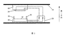
- FIG. 1 is a schematic structural view 1 of a measuring device according to an embodiment of the present disclosure
- FIG. 2 is a schematic structural view 2 of a measuring device according to an embodiment of the present disclosure
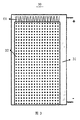
- FIG. 3 is a schematic top view of a conductive detecting portion according to an embodiment of the present disclosure
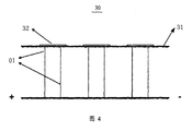
- FIG. 4 is a schematic side view of a conductive detecting portion according to an embodiment of the present disclosure.
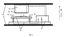
- FIG. 5 is a schematic structural diagram of a measurement system according to an embodiment of the present disclosure.
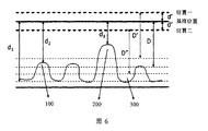
- FIG. 6 is a schematic diagram of a measurement process of a measurement system according to an embodiment of the present disclosure.
- the embodiment of the present disclosure provides a measuring device, as shown in FIG. 1 , including a housing 10 , a power source 20 , a conductive detecting portion 30 disposed in the housing 10 and connected to the power source 20 , and a bearing opposite to the conductive detecting portion 30 .
- a table 40 a terminal 50 disposed on the carrier 40 and connected to the power source 20, and a lifting mechanism 60 for controlling the relative movement of the conductive detecting portion 30 and the carrier 40 in the first direction; wherein the bearing surface 41 of the carrier 40 and The main surface of the conductive detecting portion 30 (i.e., the lower surface in Fig. 1) or the working surface is parallel, and the first direction is a direction perpendicular to the bearing surface 41.
- the carrying platform 40 is opposite to the conductive detecting portion 30, that is, the orthographic projection of the conductive detecting portion 30 on the plane of the carrying platform 40 falls on the carrying platform 40, and the conductive detecting portion 30 in FIG.
- the conductive detecting portion 30 is disposed directly above the stage 40 in relation to the positional relationship of the stage 40.
- the power source 20, as shown in FIG. 1, may be disposed inside the casing 10; or may be disposed outside the casing 10.
- FIG. 1 is only schematic and is not limited.
- the conductive detecting portion 30 and the carrying table 40 are relatively moved in the first direction, that is, the conductive detecting portion 30 can be moved in the first direction while the carrying platform 40 remains stationary; or the carrying platform 40 can be moved in the first direction.
- the conductive detecting portion 30 remains stationary; of course, both the conductive detecting portion 30 and the carrying platform 40 may be moved.
- the position of the lifting mechanism 60 is not limited, and the lifting mechanism 60 drives the conductive detecting portion 30 to move in the first direction.
- the lifting mechanism 60 is fixed to the housing 10 opposite to the carrying platform 40 .
- the inner wall (the upper wall of the casing 10 in FIG. 1) moves the conductive detecting portion 30 in the first direction; or as shown in FIG. 2, is disposed on the inner wall of the housing 10 of the casing 10 (FIG. 1)
- the lower wall of the casing 10 is configured to drive the conductive detecting portion 30 to move in the first direction; of course, other positions that can move the conductive detecting portion 30 in the first direction are also possible.
- the specific structure of the elevating mechanism 60 is not limited, and the related art may have a telescopic function or a structure capable of driving the conductive detecting portion 30 to move.
- the carrying platform 40 may be, for example, a structure disposed in the casing 10; or the inner wall of the casing 10 may be directly used as a carrying platform, and the inner wall surface is a bearing surface; the bearing surface 41 and the conductive detecting portion 30 are ensured.
- the main surface is parallel.
- the terminal 50 is disposed on the carrying platform 40, and the material of the carrying platform 40 is an insulating material.
- the bearing surface 41 of the carrying platform 40 is parallel to the main surface of the conductive detecting portion 30.
- the power is turned on, and the conductive detecting portion 30 is also energized to adjust the voltage to the required test voltage. At this time, a capacitance can be formed between the display substrate to be detected and the conductive detecting portion 30.
- terminal 50 should include positive and negative terminals, respectively.
- FIGS. 1 and 2 For the sake of simplicity, no distinction is made in FIGS. 1 and 2.
- the measuring device provided by the embodiment of the present disclosure can quickly and accurately measure the height of each spacer by using the principle of capacitive sensing, thereby obtaining an average value of different regions on the entire display substrate to be measured, and solving the optical method for determining the spacer. Highly inefficient and limited number of measured data samples.
- the measuring device provided by the embodiment of the present disclosure measures the distribution of the height of the spacer, and can accurately confirm the correlation between the abnormality of the display substrate and the height of the spacer, thereby shortening the analysis time of the display substrate and improving the yield improvement. effectiveness.
- the elevating mechanism 60 drives the conductive detecting portion 30 to move up and down in the first direction.
- the lifting mechanism 60 By causing the lifting mechanism 60 to drive the conductive detecting portion 30 to move, the height of the carrying platform 40 can be ensured and the accuracy of the measurement result can be improved without artificially adjusting the height of the carrying platform 40.
- the elevating mechanism 60 is disposed on an inner wall of the casing 10 opposite to the stage 40, and the conductive detecting portion 30 is disposed on a side of the elevating mechanism 60 facing the stage 40.
- the base of the elevating mechanism 60 is fixed to the inner wall of the casing 10, and the elevating member thereof is movable up and down with respect to the inner wall of the casing 10.
- the conductive detecting portion 30 is fixed to the elevating member of the elevating mechanism 60 to move up and down.
- the conductive detecting portion 30 faces the bearing surface 41 of the stage 40, and has no other structure between the conductive detecting portion 30 and the bearing surface 41 of the stage 40.
- the base of the lifting mechanism 60 can also be disposed on the inner wall of the side of the housing 10 of the housing 10, and is electrically conductive through an L-shaped telescopic rod or an L-shaped transmission chain or an L-shaped sliding rail.
- the detecting unit 30 is connected. Others are similar to the situation of Figure 1.
- the embodiment of the present disclosure has a simple structure and high stability by directly arranging the lifting mechanism 60 on the inner wall of the casing 10.
- the conductive detecting portion 30 includes a substrate 31, and a plurality of conductive sheets 32 disposed on the surface of the substrate 31, and the plurality of conductive sheets 32 are connected in parallel to the power source 20.
- the arrangement of the conductive sheets 32 is not limited. Alternatively, the conductive sheets 32 are arranged as densely as possible, but the conductive sheets 32 are not in contact with each other.
- the material of the conductive sheet 32 may be, for example, a metal.
- the conductive sheet 32 is connected to the power source 20 through a conductive wire 01.
- the conductive detecting portion 30 By making the conductive detecting portion 30 include a plurality of conductive sheets 32 separated from each other and in parallel, the height of the spacers (including the main spacer and the secondary spacer) corresponding thereto can be measured by the respective conductive sheets 32. , integrated into the central coordinate of the position of each conductive sheet 32, the height distribution map of the main spacer and the auxiliary spacer of the entire display substrate to be detected can be formed, thereby quickly determining the display effect of the spacers everywhere. influences.
- the conductive sheet is a polygon, and the longest connection between the vertices of the polygon is 0.5 to 1 mm.
- the conductive sheet is circular, and the diameter of the circle is 0.5 to 1 mm. This arrangement facilitates the matching of the conductive sheets to the arrangement of the spacers on the display substrate.
- a plurality of conductive sheets 32 are arranged in an array.
- the number of the spacers detected by each of the conductive sheets 32 can be the same, and the uniformity of the detection result can be improved.
- the conductive sheet 32 has a thickness of 0.001 to 1 mm.
- the conductive sheet 32 By setting the thickness of the conductive sheet 32 to 0.001 to 1 mm, the conductive sheet 32 can be prevented from being too thin to cause excessive resistance, or the conductive sheet 32 is too thick to cause inaccurate detection results.
- the power source 20 is disposed inside the casing 10.
- the housing 10 is optionally made of an insulating material.
- the orthographic projection of the housing 10 on the bearing surface 41 of the carrier 40 is rectangular.
- the embodiment of the present disclosure further provides a measurement system, as shown in FIG. 5, including the above-mentioned measuring device, and a display substrate 70 provided with a spacer; the display substrate 70 is placed on the bearing surface 41 of the measuring device, and is displayed The upper surface of the substrate 70 is covered with a conductive film; wherein the surface of the display substrate 70 covered with the conductive film is away from the bearing surface 41.
- the display substrate 70 and the conductive detecting portion 30 face each other.
- the display substrate 70 may be, for example, a color filter substrate.
- the upper surface of the display substrate 70 refers to the surface on which the display substrate 70 is provided with the spacer, that is, the spacer is away from the surface of the substrate of the display substrate 70, and a layer is coated on the surface of the spacer. Conductive film.
- the surface of the display substrate 70 covered with the conductive film should face the conductive detecting portion 30.
- the measurement method of the measurement system can be as follows:
- the lifting mechanism 60 is operated by the computer to raise and lower, and the lifting mechanism 60 drives the conductive detecting unit 30 to move to the initial position.
- the display substrate 70 coated with the conductive film layer is placed on the carrying surface 41 and connected to the positive and negative terminals 50 on the stage 40.
- the capacitance value between the conductive detecting unit 30 and the display substrate 70 is measured by the principle of capacitive sensing.
- steps S30 and S40 are repeated; if it is not necessary to continue the measurement, the measurement is ended.
- D is an effective distance between the working surface of the conductive detecting portion 30 (the lower surface of the conductive detecting portion 30 in FIG. 5) and the display substrate 70
- ⁇ 0 is a vacuum dielectric constant
- ⁇ ⁇ is a relative dielectric constant
- S is an effective area of the plate capacitor formed by the conductive detecting portion 30 and the display substrate 70
- C is a measured capacitance value.
- d 1 is the distance between the working surface of the conductive detecting portion 30 and the upper surface 300 of the display substrate 70
- d 2 is the distance between the working surface of the conductive detecting portion 30 and the top spacer 100 of the sub-spacer
- d 3 The distance between the working surface of the conductive detecting portion 30 and the main spacer top plane 200
- D is the effective distance between the working surface of the predetermined conductive detecting portion 30 and the display substrate 70.
- the area ratios of the substrate plane 300, the sub-spacer top plane 100, and the main spacer top plane 200 are calculated according to the design of the product spacers as S 1 , S 2 , and S 3 , respectively . From (Formula 1):
- the adjustment elevating mechanism 60 sequentially goes to the reference position, the position one, and the position two, and measures the capacitance between the conductive detecting portion 30 and the display substrate 70, and converts them into effective distances D, D', and D". Equation 2) is available:
- D, D' and D" and S 1 , S 2 and S 3 , and d' are known parameters, which are calculated by (data formula 3), (formula 4) and (formula 5) by data processing software Matlab.
- d 1 , d 2 and d 3 are available.
- the height values of the primary and secondary spacers are calculated by (Formula 6) and (Formula 7).
- the conductive detecting portion 30 includes a plurality of conductive sheets 32
- the height values of the main and auxiliary spacers corresponding to the respective conductive sheets 32 are respectively calculated and integrated into the position center coordinates of the conductive sheet 32 to form an entire display.
- the height distribution map of the main and sub-spacers of the substrate 70 is output as an Excel file.
- the embodiment of the present disclosure provides a measurement system for quickly and accurately measuring the height of each spacer by utilizing the principle of capacitive sensing, thereby obtaining an average value of different regions on the entire display substrate to be measured, and solving the optical method for determining the spacer.
- the problem is that the object is highly inefficient and the measured data is poorly representative.
- the correlation between the abnormality of the substrate 70 for display and the height of the spacer can be accurately confirmed, thereby shortening the analysis time of the display substrate and improving the yield. Increased efficiency.
- the conductive film has a thickness of 0.001 to 1 mm.
- a conductive film having a thickness of 0.001 to 1 mm is deposited on the upper surface of the display substrate 70, and may be, for example, a metal thin film.
- the conductive sheet 32 By setting the thickness of the conductive sheet 32 to 0.001 to 1 mm, the conductive sheet 32 can be prevented from being too thin to cause excessive resistance, or the conductive sheet 32 is too thick to cause inaccurate detection results.
Landscapes
- Physics & Mathematics (AREA)
- Nonlinear Science (AREA)
- Chemical & Material Sciences (AREA)
- Crystallography & Structural Chemistry (AREA)
- General Physics & Mathematics (AREA)
- Optics & Photonics (AREA)
- Mathematical Physics (AREA)
- Measurement Of Length, Angles, Or The Like Using Electric Or Magnetic Means (AREA)
- Investigating Or Analyzing Materials By The Use Of Electric Means (AREA)
Abstract
一种测量装置,其包括:壳体(10)、电源(20)、设置在所述壳体(10)内且与所述电源(20)连接的导电检测部(30)、与所述导电检测部(30)正对的承载台(40)、设置在所述承载台(40)上且与所述电源(20)连接的接线端子(50)、以及控制所述导电检测部(30)与所述承载台(40)沿第一方向相对移动的升降机构(60);其中,所述承载台(40)的承载面(41)和所述导电检测部(30)的主表面平行,所述第一方向为与所述承载面(41)垂直的方向。
Description
相关申请
本申请要求保护在2017年6月20日提交的申请号为201720723557.7的中国专利申请的优先权,该申请的全部内容以引用的方式结合到本文中。
本公开涉及显示技术领域,尤其涉及一种显示器基板的测量装置、及测量系统。
液晶显示器(Liquid Crystal Display,简称LCD)具有机身轻薄、耗电低、无辐射、使用寿命长等优点而被广泛的应用。
由于液晶层的厚度对LCD的响应速度、对比度、可视角度有极大影响,通常本领域技术人员通过在对盒的两个基板之间设置隔垫物(spacer)来调整LCD内部液晶层的厚度。隔垫物的高度对液晶层的厚度有着直接的影响,因此,在针对隔垫物的研究分析中,高度是重要的测量参数之一。
目前,隔垫物高度的测量方法主要为光学法,其优点为测量精度高,但同时也存在着测量效率低、测量设备复杂等问题。尤其对于高分辨率显示产品,其内部隔垫物数量较多,以所测量的有限数量的隔垫物高度数据代表整体隔垫物高度的分布情况显然存在着明显的误差。这样一来,在分析LCD异常与隔垫物高度的相关性时,难以准确得到分析结果,导致分析LCD不良原因的难度加大,所需时间增长。
公开内容
有鉴于此,本公开的第一方面提供一种测量装置,包括:壳体、电源、设置在所述壳体内且与所述电源连接的导电检测部、与所述导电检测部正对的承载台、设置在所述承载台上且与所述电源连接的接线端子、以及控制所述导电检测部与所述承载台沿第一方向相对移动的升降机构;其中,所述承载台的承载面和所述导电检测部的工作表面平行,所述第一方向为与所述承载面垂直的方向。
根据本公开的一个方面,所述升降机构带动所述导电检测部沿第一方向移动。
根据本公开的一个方面,所述升降机构设置在所述壳体中与所述承载台正对的内壁上,所述导电检测部设置在所述升降机构正对所述承载台一侧。
根据本公开的一个方面,所述导电检测部包括基板、设置在所述基板表面的多个导电片,多个所述导电片以并联的方式与所述电源连接。
可选的,所述导电片为多边形,多边形顶点之间的最长连线为0.5~1mm。
可选的,所述导电片为圆形,圆形的直径为0.5~1mm。
根据本公开的一个方面,多个所述导电片阵列排布。
根据本公开的一个方面,所述导电片的厚度为0.001~1mm。
根据本公开的一个方面,所述电源设置在所述壳体内部。
根据本公开的一个方面,所述壳体为绝缘材料。
根据本公开的一个方面,所述壳体在承载台的承载面上的正投影为矩形。
本公开的一个实施例还提供一种测量系统,包括:上述的测量装置,以及设有隔垫物的显示用基板;其中,所述显示用基板放置于所述测量装置的承载面上,且所述显示用基板的上表面覆盖一层导电薄膜。
根据本公开的一个方面,所述导电薄膜的厚度为0.001~1mm。
本公开实施例提供的测量装置、及测量系统,可利用电容感应原理快速、准确的测量出各隔垫物的高度,从而得出整个待测量显示基板上不同区域的平均值,解决了光学法测定隔垫物高度效率低下以及所测数据代表性较差的问题。通过本公开实施例提供的测量装置测定的隔垫物高度的分布情况,可准确地确认显示基板异常与隔垫物高度的相关性,从而缩短对显示基板不良的分析时间,提高良率提升的效率。本公开实施例所提供的测量装置及测量系统,可解决因取样量较少,而导致所得到的隔垫物高度分布情况存在明显误差的问题。
为了更清楚地说明本公开实施例的技术方案,下面将对本公开实施例中所需要使用的附图作简单地介绍,显而易见地,下面描述中的附图仅仅是本公开的一些实施例,对于本领域普通技术人员来讲,在 不付出创造性劳动的前提下,还可以根据这些附图获得其他的附图。
图1为本公开实施例提供的一种测量装置的结构示意图一;
图2为本公开实施例提供的一种测量装置的结构示意图二;
图3为本公开实施例提供的一种导电检测部的俯视示意图;
图4为本公开实施例提供的一种导电检测部的侧视示意图;
图5为本公开实施例提供的一种测量系统的结构示意图;
图6为本公开实施例提供的一种测量系统测量过程示意图。
下面将结合本公开实施例中的附图,对本公开实施例中的技术方案进行清楚、完整地描述,显然,所描述的实施例仅仅是本公开一部分实施例,而不是全部的实施例。基于本公开中的实施例,本领域普通技术人员在没有做出创造性劳动前提下所获得的所有其他实施例,都属于本公开保护的范围。
本公开实施例提供一种测量装置,如图1所示,包括壳体10、电源20、设置在壳体10内且与电源20连接的导电检测部30、与导电检测部30正对的承载台40、设置在承载台40上且与电源20连接的接线端子50、以及控制导电检测部30与承载台40沿第一方向相对移动的升降机构60;其中,承载台40的承载面41和导电检测部30的主表面(即图1中的下表面)或工作表面平行,第一方向为与承载面41垂直的方向。
需要说明的是,第一,承载台40与导电检测部30正对,即,导电检测部30在承载台40所在平面上的正投影落在承载台40上,以图1中导电检测部30与承载台40的位置关系来说,导电检测部30设置在承载台40的正上方。
第二,电源20,如图1所示,可以设置在壳体10内部;也可以设置在壳体10外部,图1仅为示意,不做任何限定。
第三,导电检测部30与承载台40沿第一方向相对移动,即,可以是导电检测部30沿第一方向移动而承载台40保持不动;也可以是承载台40沿第一方向移动而导电检测部30保持不动;当然还可以是导电检测部30与承载台40均移动。
其中,不对升降机构60的设置位置进行限定,以升降机构60带动导电检测部30沿第一方向移动为例,可以如图1所示,升降机构60 固定在壳体10的与承载台40相对的内壁(图1中壳体10的上壁)上以带动导电检测部30沿第一方向移动;也可以如图2所示,设置在壳体10的承载台40所在的内壁(图1中壳体10的下壁)上以带动导电检测部30沿第一方向移动;当然还可以是其他可以带动导电检测部30沿第一方向移动的设置位置。
此外,不对升降机构60的具体结构进行限定,相关技术中具有伸缩功能,或者能够带动导电检测部30移动的结构均可。
第四,承载台40,例如可以是设置在壳体10内的结构;也可以直接以壳体10的内壁作为承载台,此时内壁表面即为承载面;确保承载面41与导电检测部30的主表面平行即可。
其中,接线端子50设置在承载台40上,承载台40的材料为绝缘材料。
第五,承载台40的承载面41和导电检测部30的主表面平行,将待检测显示基板放置在承载面41上后通电,并使导电检测部30也通电,调节电压至所需测试电压,此时,待检测显示基板与导电检测部30之间即可形成电容。
第六,本领域技术人员应该明白,此处的接线端子50应分别包括正、负极接线端子,简明起见,图1和图2中没有进行区分。
本公开实施例提供的测量装置,通过利用电容感应原理快速、准确的测量出各隔垫物的高度,从而得出整个待测量显示基板上不同区域的平均值,解决了光学法测定隔垫物高度效率低下以及所测数据样本数量有限的问题。通过本公开实施例提供的测量装置来测量隔垫物高度的分布情况,可准确地确认显示基板异常与隔垫物高度的相关性,从而缩短对显示基板不良的分析时间,提高良率提升的效率。
根据本公开的一个方面,如图1和图2所示,升降机构60带动导电检测部30沿第一方向上下移动。
本公开通过使升降机构60带动导电检测部30移动,无需人为调整承载台40的高低,可保证承载台40的平稳,提高测量结果的准确度。
根据本公开的一个方面,如图1所示,升降机构60设置在壳体10中与承载台40正对的内壁上,导电检测部30设置在升降机构60的正对承载台40一侧。
即,升降机构60的底座固定在壳体10内壁上且其升降部件可相对于壳体10的内壁上下移动,导电检测部30固定在升降机构60的升降部件上以随之上下移动。导电检测部30与承载台40的承载面41正对,且导电检测部30与承载台40的承载面41之间没有其他结构。
当然,如图2所示,升降机构60的底座也可设置在壳体10的承载台40所在一侧的内壁上,并通过一个L形伸缩杆或L形传动链或L形滑动轨与导电检测部30相连接。其它与图1的情形类似。
本公开实施例通过将升降机构60直接设置在壳体10的内壁上,结构简单,稳定性高。
根据本公开的一个方面,如图3和图4所示,导电检测部30包括基板31、设置在基板31表面的多个导电片32,多个导电片32以并联的方式与电源20连接。
其中,不对导电片32的排布方式进行限定,可选地,导电片32尽可能密的排布,但导电片32之间互不接触。导电片32的材料,例如可以是金属。导电片32通过导电线01与电源20连接。
本公开实施例通过使导电检测部30包括多个彼此分离且并联的导电片32,可通过各个导电片32测量出与其对应的隔垫物(包括主隔垫物和副隔垫物)的高度,整合到各导电片32位置中心坐标上,即可形成整张待检测显示基板的主隔垫物和副隔垫物的高度分布图,从而快速地判断出各处隔垫物对显示效果的影响。
可选的,导电片为多边形,多边形顶点之间的最长连线为0.5~1mm。或者,导电片为圆形,圆形的直径为0.5~1mm。这样设置有利于导电片与通常显示基板上隔垫物的设置规律相匹配。
根据本公开的一个方面,如图3所示,多个导电片32以阵列方式排布。
本公开实施例通过将导电片32以阵列方式排布,可使每个导电片32检测到的隔垫物的数量相同,可提高检测结果的均一度。
根据本公开的一个方面,导电片32的厚度为0.001~1mm。
本公开实施例通过将导电片32的厚度设置为0.001~1mm,可避免导电片32太薄导致电阻过大,或者导电片32太厚导致检测结果不准确。
为了延长电源20的使用寿命,可选的,如图1和图2所示,电源 20设置在壳体10内部。
为了避免壳体10对检测结果的干扰,可选的,壳体10为绝缘材料。
基于上述,为了简化测量装置的结构,可选的,壳体10在承载台40的承载面41上的正投影为矩形。
本公开实施例还提供一种测量系统,如图5所示,包括上述测量装置,以及设有隔垫物的显示用基板70;显示用基板70放置于测量装置的承载面41上,且显示用基板70的上表面覆盖一层导电薄膜;其中,显示用基板70覆盖有导电薄膜的表面远离承载面41。
需要说明的是,第一,显示用基板70放置于测量装置的承载面41上后,显示用基板70与导电检测部30正对。
其中,显示用基板70例如可以是彩膜基板。
第二,显示用基板70的上表面,是指显示用基板70设置有隔垫物的表面,即,隔垫物远离显示用基板70衬底的表面,在隔垫物的表面涂覆一层导电薄膜。
第三,本领域技术人员应该明白,在对显示用基板70进行测量时,显示用基板70覆盖有导电薄膜的表面应与导电检测部30正对。
第四,测量系统的测量方法例如可以如下:
S10、通过计算机来操控升降机构60进行升降,使升降机构60带动导电检测部30移动到初始位置。
S20、将涂覆有导电膜层的显示用基板70放置到承载面41上,并与承载台40上的正、负极接线端子50相连。
S30、开启电源20,调节电压至所需测量电压,调整升降机构60使导电检测部30与显示用基板70的间距达到预定数值。
S40、利用电容感应原理测量导电检测部30与显示用基板70间的电容值。
S50、如需继续测量,重复步骤S30和S40;如无需继续测量,结束测量。
S60、数据处理。
其中,数据处理步骤如下:
根据平行电容板的计算公式:

其中,D为导电检测部30的工作表面(图5中导电检测部30的下表面)与显示用基板70之间的有效距离,ε
0为真空介电常数,ε
γ为相对介电常数;S为导电检测部30与显示用基板70形成的平板电容器的有效面积,C为所测电容值。
如图6所示,d
1为导电检测部30的工作表面与显示用基板70上表面300的距离,d
2为导电检测部30的工作表面与副隔垫物顶部平面100的距离;d
3为导电检测部30的工作表面与主隔垫物顶部平面200的距离;D为预设的导电检测部30的工作表面与显示用基板70间的有效距离。根据产品隔垫物的设计来计算基板平面300、副隔垫物顶部平面100和主隔垫物顶部平面200所占的面积比例分别为S
1、S
2和S
3。由(公式1)可得:
1/D=S
1/d
1+S
2/d
2+S
3/d
3 (公式2)
如图6所示,调节升降机构60依次至基准位置、位置一和位置二,测量导电检测部30与显示用基板70间的电容,并换算成有效距离D、D’和D”。由(公式2)可得:
1/D=S
1/d
1+S
2/d
2+S
3/d
3 (公式3)
1/D’=S
1/(d
1+d’)+S
2/(d
2+d’)+S
3/(d
3+d’) (公式4)
1/D”=S
1/(d
1-d’)+S
2/(d
2-d’)+S
3/(d
3-d’) (公式5)
其中,D、D’和D”、以及S
1、S
2和S
3、以及d’均为已知参数,通过数据处理软件Matlab对(公式3)、(公式4)和(公式5)计算可得d
1、d
2和d
3的若干组解。
通过显示用基板70的设计文件对上述各组解进行取舍;即可得d
1、d
2和d
3的准确数值。
主隔垫物高度=d
1-d
3 (公式6)
副隔垫物高度=d
1-d
2 (公式7)
通过(公式6)和(公式7)计算出主、副隔垫物的高度值。
其中,当导电检测部30包括多个导电片32时,分别计算各个导电片32对应的主、副隔垫物的高度值,整合到导电片32位置中心坐标上,即可形成整张显示用基板70的主、副隔垫物的高度分布图,以Excel文件形式输出。
本公开实施例提供一种测量系统,通过利用电容感应原理快速、准确的测量出各隔垫物的高度,从而得出整个待测量显示基板上不同区域的平均值,解决了光学法测定隔垫物高度效率低下以及所测数据代表性较差的问题。通过本公开实施例提供的测量系统测定的隔垫物高度的分布情况,可准确地确认显示用基板70异常与隔垫物高度的相关性,从而缩短对显示基板不良的分析时间,提高良率提升的效率。
根据本公开的一个方面,导电薄膜的厚度为0.001~1mm。
即,在对显示用基板70进行测量之前,在显示用基板70上表面蒸镀一层厚度为0.001~1mm的导电薄膜,例如可以是金属薄膜。
本公开实施例通过将导电片32的厚度设置为0.001~1mm,可避免导电片32太薄导致电阻过大,或者导电片32太厚导致检测结果不准确。
以上所述,仅为本公开的具体实施方式,但本公开的保护范围并不局限于此,任何熟悉本技术领域的技术人员在本公开揭露的技术范围内,可轻易想到变化或替换,都应涵盖在本公开的保护范围之内。因此,本公开的保护范围应以所述权利要求的保护范围为准。
Claims (12)
- 一种测量装置,其包括:壳体和电源;设置在所述壳体内且与所述电源连接的导电检测部;与所述导电检测部正对的承载台;设置在所述承载台上且与所述电源连接的接线端子;以及控制所述导电检测部与所述承载台沿第一方向相对移动的升降机构;其中,所述承载台的承载面和所述导电检测部的工作表面平行,所述第一方向为与所述承载面垂直的方向。
- 根据权利要求1所述的测量装置,其中,所述升降机构带动所述导电检测部沿第一方向移动。
- 根据权利要求2所述的测量装置,其中,所述升降机构设置在所述壳体的与所述承载台正对的内壁上,所述导电检测部设置在所述升降机构正对所述承载台一侧。
- 根据权利要求1所述的测量装置,其中,所述导电检测部包括基板、设置在所述基板表面的多个导电片,多个所述导电片以并联的方式与所述电源连接。
- 根据权利要求4所述的测量装置,其中,所述导电片为多边形,多边形顶点之间的最长连线为0.5~1mm;或者,所述导电片为圆形,圆形的直径为0.5~1mm。
- 根据权利要求4所述的测量装置,其中,多个所述导电片以阵列方式排布。
- 根据权利要求4所述的测量装置,其中,所述导电片的厚度为0.001~1mm。
- 根据权利要求1所述的测量装置,其中,所述电源设置在所述壳体内部。
- 根据权利要求1-8任一项所述的测量装置,其中,所述壳体为绝缘材料。
- 根据权利要求1-8任一项所述的测量装置,其中,所述壳体在承载台的承载面上的正投影为矩形。
- 一种测量系统,其中,包括:权利要求1-10任一项所述的测量装置,以及设有隔垫物的显示用基板;其中,所述显示用基板放置于所述测量装置的承载面上,且所述显示用基板的上表面覆盖一层导电薄膜。
- 根据权利要求11所述的测量系统,其中,所述导电薄膜的厚度为0.001~1mm。
Priority Applications (1)
| Application Number | Priority Date | Filing Date | Title |
|---|---|---|---|
| US16/095,818 US10983376B2 (en) | 2017-06-20 | 2018-04-09 | Measuring device and a measuring system |
Applications Claiming Priority (2)
| Application Number | Priority Date | Filing Date | Title |
|---|---|---|---|
| CN201720723557.7 | 2017-06-20 | ||
| CN201720723557.7U CN206788515U (zh) | 2017-06-20 | 2017-06-20 | 一种测量装置、及测量系统 |
Publications (1)
| Publication Number | Publication Date |
|---|---|
| WO2018233348A1 true WO2018233348A1 (zh) | 2018-12-27 |
Family
ID=60717565
Family Applications (1)
| Application Number | Title | Priority Date | Filing Date |
|---|---|---|---|
| PCT/CN2018/082236 Ceased WO2018233348A1 (zh) | 2017-06-20 | 2018-04-09 | 测量装置及测量系统 |
Country Status (3)
| Country | Link |
|---|---|
| US (1) | US10983376B2 (zh) |
| CN (1) | CN206788515U (zh) |
| WO (1) | WO2018233348A1 (zh) |
Families Citing this family (3)
| Publication number | Priority date | Publication date | Assignee | Title |
|---|---|---|---|---|
| CN206788515U (zh) | 2017-06-20 | 2017-12-22 | 京东方科技集团股份有限公司 | 一种测量装置、及测量系统 |
| CN108225167A (zh) * | 2018-01-02 | 2018-06-29 | 京东方科技集团股份有限公司 | 测量装置及隔垫物高度测量方法 |
| CN113878675B (zh) * | 2021-10-21 | 2022-07-22 | 张牧春 | 一种小提琴琴箱背弧加工装置 |
Citations (5)
| Publication number | Priority date | Publication date | Assignee | Title |
|---|---|---|---|---|
| JP2007163296A (ja) * | 2005-12-14 | 2007-06-28 | Takano Co Ltd | 液晶パネルの基板間隔調整用スペーサの高さ測定方法及び装置 |
| KR20110022108A (ko) * | 2009-08-27 | 2011-03-07 | 세심광전자기술(주) | 원기를 쓴 간극제 높이 검사방법 및 검사장치 |
| CN103676240A (zh) * | 2013-12-20 | 2014-03-26 | 合肥京东方光电科技有限公司 | 表面检测装置 |
| CN106057503A (zh) * | 2016-07-15 | 2016-10-26 | 吴江佳亿电子科技有限公司 | 一种片式高压瓷介电容器电容测量装置 |
| CN206788515U (zh) * | 2017-06-20 | 2017-12-22 | 京东方科技集团股份有限公司 | 一种测量装置、及测量系统 |
Family Cites Families (1)
| Publication number | Priority date | Publication date | Assignee | Title |
|---|---|---|---|---|
| CN103424065A (zh) | 2013-07-29 | 2013-12-04 | 中国原子能科学研究院 | 一种微小距离的测定方法 |
-
2017
- 2017-06-20 CN CN201720723557.7U patent/CN206788515U/zh not_active Expired - Fee Related
-
2018
- 2018-04-09 US US16/095,818 patent/US10983376B2/en not_active Expired - Fee Related
- 2018-04-09 WO PCT/CN2018/082236 patent/WO2018233348A1/zh not_active Ceased
Patent Citations (5)
| Publication number | Priority date | Publication date | Assignee | Title |
|---|---|---|---|---|
| JP2007163296A (ja) * | 2005-12-14 | 2007-06-28 | Takano Co Ltd | 液晶パネルの基板間隔調整用スペーサの高さ測定方法及び装置 |
| KR20110022108A (ko) * | 2009-08-27 | 2011-03-07 | 세심광전자기술(주) | 원기를 쓴 간극제 높이 검사방법 및 검사장치 |
| CN103676240A (zh) * | 2013-12-20 | 2014-03-26 | 合肥京东方光电科技有限公司 | 表面检测装置 |
| CN106057503A (zh) * | 2016-07-15 | 2016-10-26 | 吴江佳亿电子科技有限公司 | 一种片式高压瓷介电容器电容测量装置 |
| CN206788515U (zh) * | 2017-06-20 | 2017-12-22 | 京东方科技集团股份有限公司 | 一种测量装置、及测量系统 |
Also Published As
| Publication number | Publication date |
|---|---|
| US10983376B2 (en) | 2021-04-20 |
| CN206788515U (zh) | 2017-12-22 |
| US20200341304A1 (en) | 2020-10-29 |
Similar Documents
| Publication | Publication Date | Title |
|---|---|---|
| JP5989120B2 (ja) | 非接触容量式間隔センサ装置および非接触容量式間隔検査方法 | |
| WO2018233348A1 (zh) | 测量装置及测量系统 | |
| CN103592548B (zh) | 基于位图追踪法的双探针自动测试平台的样品测试方法 | |
| US10802063B2 (en) | Detection device and detection method | |
| CN104698632A (zh) | 一种基板检测装置及突起高度检测方法 | |
| CN107422241B (zh) | 使用探针卡的方法及系统 | |
| CN104457907B (zh) | 一种用于测量绝缘容器内液位的非接触式检测装置 | |
| US10139441B2 (en) | Film structure and its measuring method, display substrate and its measuring method and manufacturing method | |
| CN104048604A (zh) | 电池尺寸光学测量方法及其系统 | |
| WO2017067365A1 (zh) | 检测装置、基板架、检测基板架上基板位置的方法 | |
| WO2018036200A1 (zh) | 膜层测试结构及阵列基板 | |
| KR20110087758A (ko) | 정밀도가 높은 정전용량방식 터치스크린 장치 | |
| CN104089582A (zh) | 金属膜光学检测装置和检测方法 | |
| CN209372015U (zh) | 视觉测量系统 | |
| CN101432632B (zh) | 用于检查印制电路结构的传感器、装置和方法以及传感器的加工方法 | |
| CN115342740A (zh) | 一种铜箔测厚设备 | |
| CN104536169B (zh) | 一种用于获取阵列基板中电容容值的结构体及方法 | |
| CN103424065A (zh) | 一种微小距离的测定方法 | |
| WO2018126685A1 (zh) | 溅射缝隙测量工具、磁控溅射设备 | |
| WO2017049825A1 (zh) | 对位装置及对位检测方法 | |
| CN108007774A (zh) | 测定片状材料杨氏模量的装置和方法 | |
| TWI616664B (zh) | 使用探針卡之方法、系統及其探針卡裝置 | |
| CN108225167A (zh) | 测量装置及隔垫物高度测量方法 | |
| CN108061983A (zh) | 配向膜边界到显示区的距离的测量方法及测量装置 | |
| CN112179517A (zh) | 温度传感器以及温度检测方法 |
Legal Events
| Date | Code | Title | Description |
|---|---|---|---|
| 121 | Ep: the epo has been informed by wipo that ep was designated in this application |
Ref document number: 18819757 Country of ref document: EP Kind code of ref document: A1 |
|
| NENP | Non-entry into the national phase |
Ref country code: DE |
|
| 32PN | Ep: public notification in the ep bulletin as address of the adressee cannot be established |
Free format text: NOTING OF LOSS OF RIGHTS PURSUANT TO RULE 112(1) EPC (EPO FORM 1205A DATED 29.05.2020) |
|
| 122 | Ep: pct application non-entry in european phase |
Ref document number: 18819757 Country of ref document: EP Kind code of ref document: A1 |